ee-‐382m vlsi–ii early design planning: front end spring...
TRANSCRIPT

EE382M-‐8 Class Notes
EE-‐382M VLSI–II Early Design Planning: Front End Spring 2017
Mark McDermoF Jacob Abraham Gian Gerosa
1/24/17 1/24/17 Page 1

EE382M-‐8 Class Notes
TLAs
§ EDP – Early Design Planning § FE – Front End § BE – Back End § SOC – System-‐on-‐Chip § SC – Standard Cell § SDP – Structured Datapath § PD – Physical Design § STA – StaRc Timing Analysis § .LIB – STA Library § ABGEN – Abstract Generator § APR – Auto Place & Route § LEF – Library Exchange Format § DEF – Design Exchange Format § TTM – Time to Money
Page 2 1/24/17

EE382M-‐8 Class Notes
Agenda
§ Early Design Planning (EDP) objecRves § EDP-‐FE Flow
– Design parRRoning – Area esRmaRon – Block & Unit floorplanning – Block & Unit route planning – Chip level floorplanning – Chip level route planning – Chip & block level power esRmaRon – Chip & block level Rming esRmaRon
§ Summary
Page 3 1/24/17

EE382M-‐8 Class Notes
EDP-‐FE ObjecRves
§ Get designers thinking about physical implementaRon while doing the architecture design. – Avoids pi^alls that can cause die size growth, Rming issues and power distribuRon problems.
§ Give designers a procedure to floorplan high performance SOCs. – Becomes the starRng point for the chip plan iteraRon.
§ It is the starRng point for block/unit/parRRon/cluster design by sebng various constraints such as block size and placement, feed-‐through plan, power and clock distribuRon.
Page 4 1/24/17 1/24/17 4

EE382M-‐8 Class Notes
Design Flow Paradigm
• HW/SW Architecture, µarchitecture, logic, floorplan, Rming, power opRmized concurrently.
• Clusters and top level chip opRmized in parallel
• Top-‐down budgeRng with boFom-‐up feedback
• Forward constraint-‐driven (Rming,…) and back-‐annotaRon (parasiRc, area)
Cell Level
Bottom-Up Feedback
Top-down Budgeting
Architecture Level
Cell Level
Analysis: Back Annotation
Planning: Forward Constraint Driven
Architecture Level
1/24/17 Page 5
EE382M-‐8 Class Notes
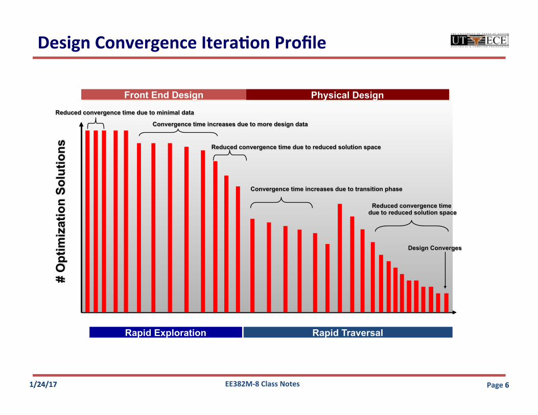
Design Convergence IteraRon Profile
6 1/24/17
Front End Design Physical Design
Rapid Exploration Rapid Traversal
# O
ptim
izat
ion
Solu
tions
Design Converges
Reduced convergence time due to minimal data
Convergence time increases due to more design data
Reduced convergence time due to reduced solution space
Convergence time increases due to transition phase
Reduced convergence time due to reduced solution space
1/24/17 Page 6
EE382M-‐8 Class Notes
Netlist Layout
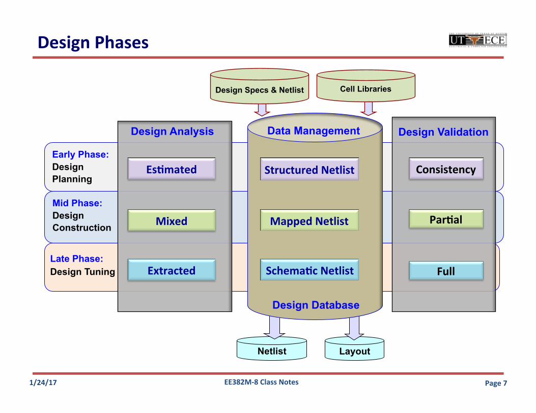
Design Phases
Page 7 1/24/17
Early Phase: Design Planning
Mid Phase: Design Construction
Late Phase: Design Tuning
EsRmated
Design Specs & Netlist
Cell Libraries
Consistency
Data Management
SchemaRc Netlist
Mixed
Extracted
ParRal
Full
Mapped Netlist
Structured Netlist
Design Analysis Design Validation
Design Database
EE382M-‐8 Class Notes
Floorplan
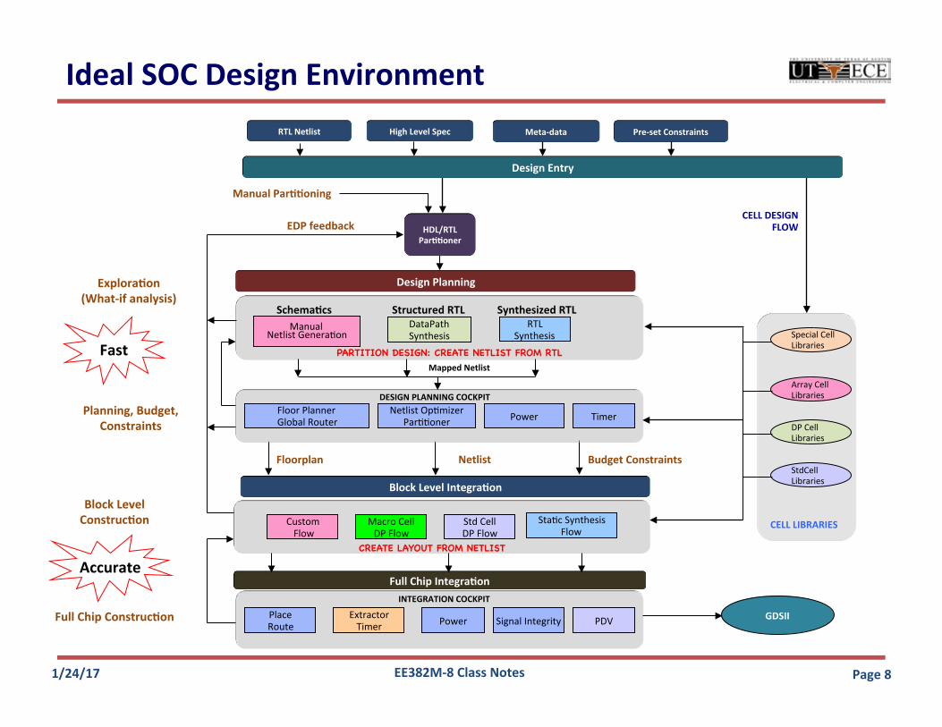
Design Planning
Full Chip IntegraRon
Block Level IntegraRon
Manual Netlist Genera/on
RTL Synthesis
DataPath Synthesis
Netlist Op/mizer Par//oner
Mapped Netlist
Macro Cell DP Flow
Sta/c Synthesis Flow
Std Cell DP Flow
Custom Flow
Floor Planner Global Router
EDP feedback
Netlist StdCell Libraries
DP Cell Libraries
Array Cell Libraries
CELL LIBRARIES
Manual ParRRoning
PARTITION DESIGN: CREATE NETLIST FROM RTL
CREATE LAYOUT FROM NETLIST
Special Cell Libraries
Budget Constraints
Power Timer
ExploraRon (What-‐if analysis)
Planning, Budget, Constraints
SchemaRcs Structured RTL Synthesized RTL
Extractor Timer
Place Route Signal Integrity PDV Power
CELL DESIGN FLOW
GDSII
High Level Spec RTL Netlist Pre-‐set Constraints
DESIGN PLANNING COCKPIT
INTEGRATION COCKPIT
HDL/RTL ParRRoner
Full Chip ConstrucRon
Block Level ConstrucRon
Meta-‐data
Fast
Accurate
Ideal SOC Design Environment
Design Entry
1/24/17 Page 8

EE382M-‐8 Class Notes
EE382M Design Flow
Page 9 1/24/17
Early Design Planning AcRviRes Physical Design AcRviRes Front End Design AcRviRes
Logic/Memory Synthesis
Logic/Circuit Design
Logic ParRRoning,
Area EsRmaRon
& Block
Planning
Logic & Mixed-‐Mode SimulaRon
Chip/Block Level Floorplanning
Design VerificaRon
EsRmated Power Analysis
I/O Pin Placement
Power/GND Planning/RouRng
EsRmated Timing Analysis
Global Placement
Detail Placement
Clock Tree Synthesis & RouRng
Global & Detail RouRng
ExtracRon, Delay CalculaRon
& Detailed Timing
Analysis
Behavioral Level Design

EE382M-‐8 Class Notes
Agenda
§ Early Design Planning (EDP) objecRves § EDP-‐FE Flow
– Design parRRoning – Area esRmaRon – Block & Unit planning – Block & Unit route planning – Chip level floorplanning – Chip level route planning – Chip & block level power esRmaRon – Chip & block level Rming esRmaRon
§ Summary
Page 10 1/24/17

EE382M-‐8 Class Notes
EDP-‐FE Flow
Page 11 1/24/17
Design ParRRoning
Area EsRmaRon
Unit/Cell Planning
Logical vs. Physical Synthesis or Custom
Synthesis or Manual EsRmaRon
Block Planning Floorplanning Tool
ABGEN Tool .LIB Generator
Block Level Route Planning Global RouRng Tool
Logic Synthesis
Logic Design
Behavioral Level Design
Memory Synthesis
Circuit Design
Front End Design
EDP-‐FE Flow

EE382M-‐8 Class Notes
EDP-‐FE Flow
EDP-‐FE Flow (cont)
Page 12 1/24/17
Chip Level Floorplanning
EsRmated Timing Analysis
Floorplanning Tool
Physical Synthesis Manual (Spreadsheet) Analysis
EsRmated Power Analysis
Physical Synthesis Power EsRmaRon Tools
Manual (Spreadsheet) Analysis
To Back End EDP
All Constraints
Met?
Y
N To Front End Design Flow
Chip Level Route Planning
Global RouRng Tool Clock tree synthesis tool

EE382M-‐8 Class Notes
ParRRoning: Building Blocks
§ Three types of building blocks are used in a VLSI chip: – SC: Standard Cell Block • Typically synthesized using standard cell library • Layout is done using AutomaRc Place & Route (APR) tools
– SDP: Structured Data Paths • Typically designed using DP libraries or the standard cell library used for SCs. • Layout is generated using Rling engines using relaRve placement constraints. • RouRng can be done manually (for busses, clocks) or with automated routers or a mix of both.
– Customs Macros: Memory arrays, Register Files, CAMs, PLLs, Thermal sensors, off-‐chip IO buffers, voltage regulators, etc. • Memory generators can be used; High performance arrays are typically done manually. Memory generators will produce layout. Custom designed memories will be done manually.
• Semicustom design is also used: leaf cells are pure custom, but block can be built with AP&R tools.
Page 13 1/24/17 1/24/17 13

EE382M-‐8 Class Notes
Chip
Block
Unit
Sub-unit
Cells
Logical Physical
SC lib SDP lib Arrays Arrays
ParRRoning: Logical vs. Physical Mapping
SC lib SDP lib
1/24/17 14 1/24/17 Page 14

EE382M-‐8 Class Notes
Area EsRmaRon
§ Area esRmaRon is accomplished using one of these three methods: – Scaling from previous design • Reasonably accurate method. • Modify area by direct mulRplicaRon of previous area by scaling factor • Scaling factor is determined by process technology group
– Scaling factor may be be non-‐linear due to process scaling issues.
– Manual esRmaRon using spreadsheets • Least accurate method. • Requires esRmaRng the number of logical elements that will be used. • Requires esRmaRng size of hard macros
– Synthesis of an exisRng design • Most reliable method. Not always possible during early design phase • Need to add “fudge” factor to accommodate future growth (or shrinkage) • Need to esRmate SC uRlizaRon percentages.
Page 15 1/24/17

EE382M-‐8 Class Notes
Block Size EsRmaRon Spreadsheet Example
§ The block area esRmaRons are done using the same spreadsheet as the power esRmaRon; since the project will use synthesis, then results can be obtained arer APR steps.
§ The spreadsheet comprehends the following: – Area uRlizaRon factors for each gate type – Block uRlizaRon factors
1/24/17 16
Technology
Cell Type Area µ2
Typical SC Density
gates/mm2Area µ2
Typical SC Density
gates/mm2Area µ2
Typical SC Density
gates/mm2Area µ2
Typical SC Density
gates/mm2Area µ2
Typical SC Density
gates/mm2
INV 26.8 28,006 9.7 77,160 3.5 204,082 1.3 562,266 0.5 1,549,0992-‐NAND 28.6 26,247 11.9 63,131 4.9 145,773 2.1 350,619 0.9 843,3263-‐NAND 26.4 28,447 16.2 46,296 10.0 72,333 6.1 117,721 3.8 191,5894-‐NAND 43.9 17,068 27.0 27,778 10.0 72,333 3.7 196,201 1.4 532,1902-‐NOR 28.6 26,247 11.9 63,131 4.9 145,773 2.1 350,619 0.9 843,3263-‐NOR 81.0 9,259 22.7 33,069 6.4 113,379 1.8 404,924 0.5 1,446,1574-‐NOR 76.7 9,780 29.2 25,720 11.1 64,935 4.2 170,771 1.6 449,105DFFR 103.7 7,229 44.3 16,938 18.9 38,095 8.1 89,252 3.4 209,104SDFFR 107.5 6,980 57.2 13,103 30.5 23,613 16.2 44,326 8.7 83,210
Average 17,696 40,703 97,813 254,078 683,012
180nm 130nm 90nm 65nm 45nm
1/24/17 Page 16

EE382M-‐8 Class Notes
Block Size EsRmaRon Spreadsheet Example
UNIT:
inv 3 2812 1.2 80.0% 4218 2.00buf 8 1868 2.4 80.0% 5604 2.67
triinv 15 1 4.2 80.0% 79 2.86clk_buf 22 487 5.9 80.0% 3592 2.98
and2 11 676 3.2 75.0% 2884 2.58and3 18 35 4.7 70.0% 235 2.68and4 26 89 6.1 65.0% 835 2.77
nand2 8 2285 2.9 75.0% 8835 2.07nand3 15 365 4.1 70.0% 2138 2.56nand4 24 21 6.8 65.0% 220 2.29nor2 10 1 2.9 75.0% 12 2.59nor3 21 73 4.1 70.0% 428 3.59nor4 36 57 6.8 65.0% 596 3.44xor2 30 264 6.9 75.0% 2429 3.26
xnor2 30 169 7.2 75.0% 1622 3.13aoi3 16 1640 9.0 70.0% 21086 1.24aoi4 20 0 11.0 65.0% 17 1.18oai3 16 888 13.0 70.0% 16491 0.86oai4 20 12 17.0 65.0% 314 0.76or2 15 220 3.4 75.0% 997 3.31or3 23 23 4.7 70.0% 154 3.43or4 23 23 6.2 65.0% 219 2.41
mux2 9 360 4.2 70.0% 2160 1.50imux2 15 360 6.6 70.0% 3394 1.59mux4 27 12 8.3 60.0% 166 1.95imux4 39 0 11.0 60.0% 18 2.13DFFR 36 1339 8.1 55.0% 19720 2.44
SDFFR 56 320 16.2 55.0% 9425 1.90
GateTotal Area with
Utilization Factor ( µ2)
Transistor Density
(Transistors/ µ2)
Min Sized Transistors
Actual Gate Count (USER
SPECIFIED)
PUT YOUR BLOCK NAME
GATES AREA CALCULATION
Area per Logic Gate ( µ2) Utilization Factor
1/24/17 17 1/24/17 Page 17

EE382M-‐8 Class Notes
EsRmated area calculaRon
§ The block area esRmates are determined by summing up the SC/SDP area calculaRons with the Memory area calculaRon.
Area Percentage78744.11 73.0%
FLIP FLOP AREA 29145.27 27.0%MEMORY AREA 0.00 0.0%
107889.38 100.0%
AVERAGE TRANSISTOR DENSITY 1.91
Total AREA ( µ2)
LOGIC AREA
1/24/17 18 1/24/17 Page 18

EE382M-‐8 Class Notes
Block & Unit planning
§ Block planning is used to determine: – Block pin placement • Including through cell routes
– Hard macro placement – Aspect raRo of the block(s)
Page 19 1/24/17
EE382M-‐8 Class Notes
Block & Unit route planning
§ Block level route planning is used to: – Determine criRcal paths within a block – Determine the key pre-‐routes that need to be fed to the global router – Determine preliminary power grid rouRng
Page 20 1/24/17

EE382M-‐8 Class Notes
Chip Level floorplanning
§ Chip level floorplanning – Determine starRng point(s) for block placement opRons – Determine aspect raRo opRon(s) for the chip
Page 21 1/24/17
Memory Macros Datapath Macro
EE382M-‐8 Class Notes
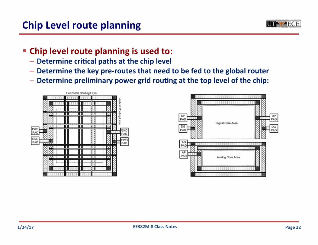
Chip Level route planning
§ Chip level route planning is used to: – Determine criRcal paths at the chip level – Determine the key pre-‐routes that need to be fed to the global router – Determine preliminary power grid rouRng at the top level of the chip:
Page 22 1/24/17

EE382M-‐8 Class Notes
Chip & Block Level power esRmaRon
§ Power esRmates for SC and SDP blocks are based on data from Design Compiler. – PTPX (Synopsys power analysis tool) will be used.
§ Final block/unit power should include the following: – Block acRvity factors – Clock power – Memory power – Logic gate intrinsic power – Transistor gate leakage power – Transistor gate capacitance power – Interconnect wiring capacitance power – Source-‐drain leakage power – Signal switching factors – Glitching or spurious acRvity power
Page 23 1/24/17 1/24/17 23

EE382M-‐8 Class Notes
AcRvity Factor vs. Switching Factor
§ AcRvity Factor represents how oren a specific block is acRve -‐ Represented as percentage of Rme -‐ For example an instrucRon fetch unit is acRve 80-‐90% of the Rme where a debug unit would be acRve 1% of the Rme
§ Switching factor is also represented as a percentage and indicates how oren the internal nodes of a specific block toggle -‐ A funcRon of the type of gate. -‐ For example Inverters switch all the Rme -‐ 4-‐input NAND gates switch considerably less -‐ Complex gates have even lower switching factors.
-‐ Typical SC blocks have switching factors of about 15-‐25% depending on the mix of logic
§ AcRvity Factor is driven by the architecture § Switching Factor is driven by circuit topology
Page 24 1/24/17 1/24/17 24

EE382M-‐8 Class Notes
AcRvity Factors (%)
Page 25 1/24/17
SoKware controlled
Runs in KHz range
Data 90% CACHE hit rate
Occurs nearly every cycle
Instruc/ons 1/24/17 25
EE382M-‐8 Class Notes
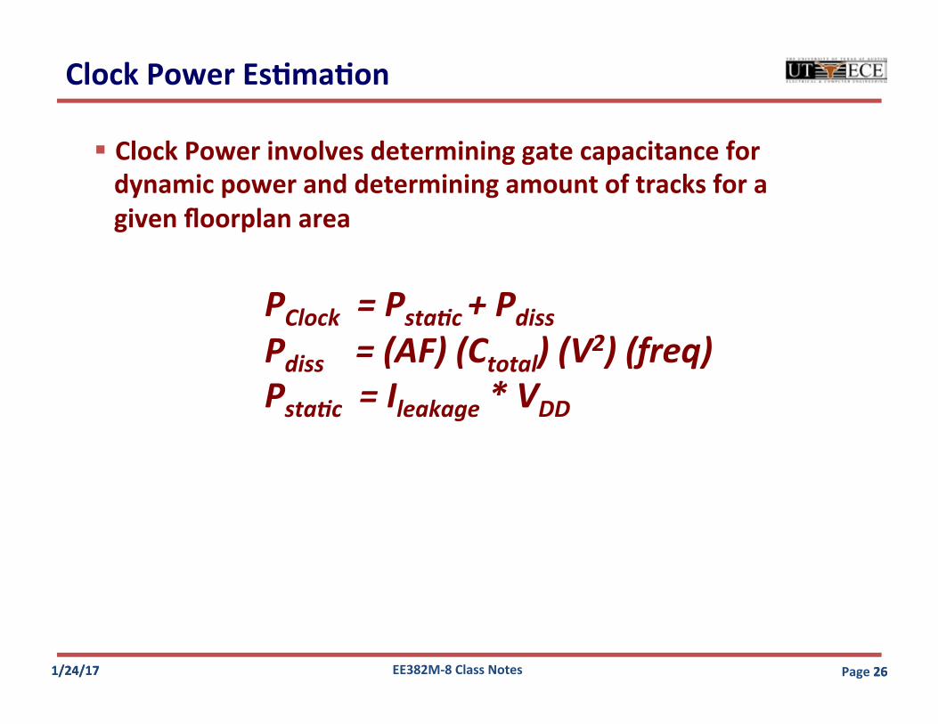
Clock Power EsRmaRon
§ Clock Power involves determining gate capacitance for dynamic power and determining amount of tracks for a given floorplan area PClock = Psta,c + Pdiss Pdiss = (AF) (Ctotal) (V2) (freq) Psta,c = Ileakage * VDD
1/24/17 26 1/24/17 Page 26

EE382M-‐8 Class Notes
Memory Power EsRmaRon
§ Most power dissipaRon for an array occurs in bit-‐lines and sense amplifiers
§ Calculate total bitline capacitance {Metal2 bitline cap} + {juncRon cap} X {number of bitcells}
§ Calculate sense node capaciRve load to include in power dissipaRon
§ For power dissipaRon, we use the approximaRon:
Pdyn = α * Ctotal * VDD * VDD * frequency Where alpha is the “AcRvity Factor” 0 < α < 1
§ Memory cells can contribute significant D.C. power due to leakage from many cells in standby; be sure to take into account
PstaRc = Ileakage * VDD
1/24/17 27 1/24/17 Page 27

EE382M-‐8 Class Notes
Logic Gate Intrinsic Power
Page 28 1/24/17
Pgate-‐intrinsic = (Tcount) (AF) (SFavg) (Cj-‐den) (A) (V2) (f) Tcount = Total Min Size Transistors AF = Ac,vity Factor SFavg = Average Switching Factor for whole block Cj-‐den = Junc,on Capacitance for 65nm = 4.1 fF/um2 A = Area of junc,on V = Vdd f = Frequency
28 1/24/17

EE382M-‐8 Class Notes
Sources of Leakage Power
Page 29 1/24/17 1/24/17 29

EE382M-‐8 Class Notes
Transistor Gate Leakage Power
Page 30 1/24/17 30 1/24/17
• Gate oxide thickness < 2nm • Direct tunneling of charge carriers through gate oxide, causing gate leakage to increase
• Was expected to grow by 500X / technology
• Was dominant leakage component • Was expected to contribute more than 15% -‐ 20% of total power
• High-‐K gate dielectrics have alleviated this problem

EE382M-‐8 Class Notes
Transistor Gate Leakage Power
Pgate-‐leakage = (Tcount) (Wmin) (L) (On%) (Gleakage) (V)
Tcount = Total Min Size Transistors Wmin = Minimum Width L = Minimum Length On% = Percent On = 50% (all blocks) Gleakage = Gate Leakage for 65nm = 15.6 nA / um2
V = Vdd
1/24/17 31 1/24/17 Page 31

EE382M-‐8 Class Notes
S-‐D Leakage Power
§ Technology scaling causing 30% smaller dimensions, causing higher energy consumpRon, power dissipaRon
§ Voltage and Vt must both be scaled to contain power increase and maintain 30% gate delay reducRon
§ Leakage increases with scaled Vdd and Vt
1/24/17 32 1/24/17 Page 32

EE382M-‐8 Class Notes
S-‐D Leakage Power
PS-‐D-‐leakage = (Tcount) (Wmin)(S-‐Dleakage) (SE) (V)
Tcount = Total Min Size Transistors Wmin = Minimum Width L = Minimum Length S-‐Dleakage= Source-‐Drain Leakage = x.xx nA / um2
SE = Stack Effect V = Vdd
1/24/17 33 1/24/17 Page 33

EE382M-‐8 Class Notes
Interconnect Power
§ Becoming large porRon of power consumpRon given smaller technologies
§ Up to 40% of total power
§ Depends on physical info of layout / packing
§ Assuming square model for block, interconnect length is esRmated at Length / 5
1/24/17 34 1/24/17 Page 34

EE382M-‐8 Class Notes
Interconnect Power
PIntercon = (Gate)(AF) (SF) (Cavg wire-‐den) (IL) (V2) (f) Gate = Total Gate Count AF = Ac,vity Factor SF = Switching Factor Cavg wire-‐den = Average Wire Capacitance for M1-‐M4 = 0.21 fF/um IL = Interconnect Length (Assume square block, divide by 5 V = Vdd f = Frequency
1/24/17 35 1/24/17 Page 35
EE382M-‐8 Class Notes
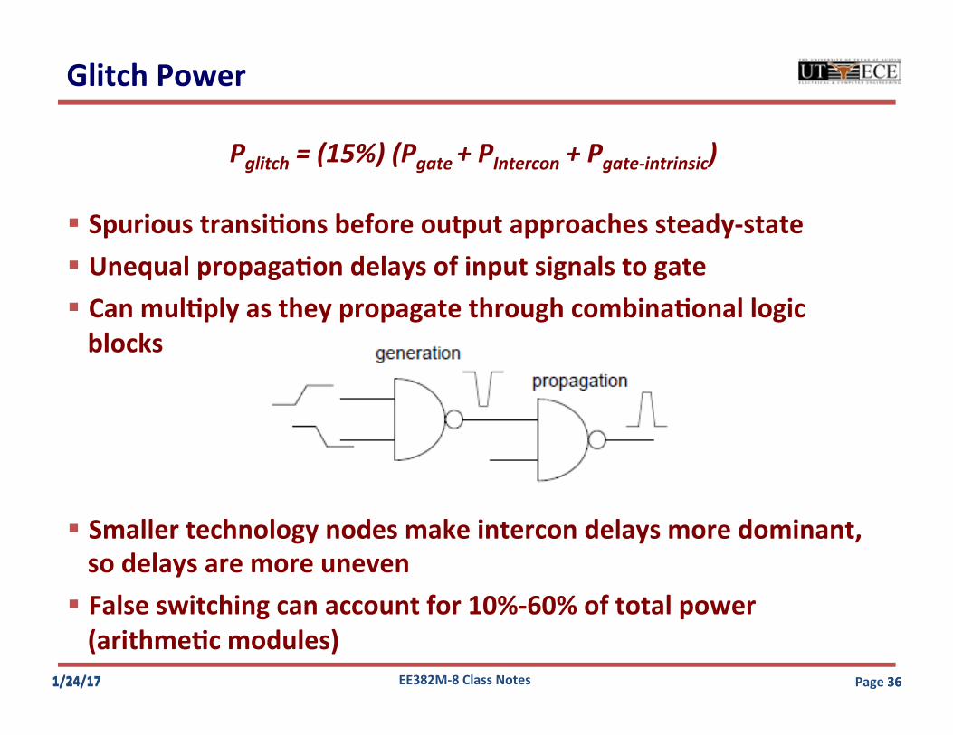
Glitch Power
Pglitch = (15%) (Pgate + PIntercon + Pgate-‐intrinsic)
§ Spurious transiRons before output approaches steady-‐state § Unequal propagaRon delays of input signals to gate § Can mulRply as they propagate through combinaRonal logic blocks
§ Smaller technology nodes make intercon delays more dominant, so delays are more uneven
§ False switching can account for 10%-‐60% of total power (arithmeRc modules)
Page 36 1/24/17 1/24/17 36

EE382M-‐8 Class Notes
Power EsRmaRon Spreadsheet Example
Gate Type Min size transistors for each gate
Gate count from synopsys run
Calculation of various types of power
Total module power AF input from user Based on target clock Freq.
1/24/17 37 1/24/17 Page 37

EE382M-‐8 Class Notes
SC and SDP Power EsRmaRon Spreadsheet
UNIT NAME:
ADDF_B 47 1 0.75 47 12.2 12% 6.1 1.725E-‐04 2.693E-‐05 3.197E-‐04 2.478E-‐06 1.210E-‐04 6.1 75.0% 8.1 5.77
ADDF_C 64 1 0.75 64 16.6 12% 8.3 2.349E-‐04 2.693E-‐05 4.354E-‐04 3.375E-‐06 1.647E-‐04 8.3 75.0% 11.1 5.77
AND2_B 14 1 0.75 14 3.6 12% 1.8 5.138E-‐05 2.693E-‐05 9.524E-‐05 7.382E-‐07 3.604E-‐05 1.8 75.0% 2.4 5.77
AND2_C 18 1 0.75 18 4.7 12% 2.3 6.606E-‐05 2.693E-‐05 1.225E-‐04 9.491E-‐07 4.633E-‐05 2.3 75.0% 3.1 5.77
AND2_D 28 1 0.75 28 7.3 12% 3.6 1.028E-‐04 2.693E-‐05 1.905E-‐04 1.476E-‐06 7.207E-‐05 3.6 75.0% 4.9 5.77
AND3_B 18 1 0.67 18 4.7 9% 2.3 6.606E-‐05 2.020E-‐05 1.225E-‐04 9.491E-‐07 4.139E-‐05 2.3 70.0% 3.3 5.38
AND3_C 22 1 0.67 22 5.7 9% 2.9 8.074E-‐05 2.020E-‐05 1.497E-‐04 1.160E-‐06 5.059E-‐05 2.9 70.0% 4.1 5.38
AND3_D 26 1 0.67 26 6.8 9% 3.4 9.542E-‐05 2.020E-‐05 1.769E-‐04 1.371E-‐06 5.979E-‐05 3.4 70.0% 4.8 5.38
AO21_B 24 1 0.50 24 6.2 6% 3.1 8.808E-‐05 1.347E-‐05 1.633E-‐04 1.265E-‐06 4.118E-‐05 3.1 70.0% 4.5 5.38
AO21_C 26 1 0.50 26 6.8 6% 3.4 9.542E-‐05 1.347E-‐05 1.769E-‐04 1.371E-‐06 4.462E-‐05 3.4 70.0% 4.8 5.38
AO21_D 32 1 0.50 32 8.3 6% 4.2 1.174E-‐04 1.347E-‐05 2.177E-‐04 1.687E-‐06 5.491E-‐05 4.2 70.0% 5.9 5.38
AO22_B 28 1 0.50 28 7.3 6% 3.6 1.028E-‐04 1.347E-‐05 1.905E-‐04 1.476E-‐06 4.805E-‐05 3.6 70.0% 5.2 5.38
AO22_C 32 1 0.50 32 8.3 6% 4.2 1.174E-‐04 1.347E-‐05 2.177E-‐04 1.687E-‐06 5.491E-‐05 4.2 70.0% 5.9 5.38
AOI21_A 20 1 0.50 20 5.2 6% 2.6 7.340E-‐05 1.347E-‐05 1.361E-‐04 1.055E-‐06 3.432E-‐05 2.6 60.0% 4.3 4.62
AOI21_B 24 1 0.50 24 6.2 6% 3.1 8.808E-‐05 1.347E-‐05 1.633E-‐04 1.265E-‐06 4.118E-‐05 3.1 70.0% 4.5 5.38
AOI21_C 30 1 0.50 30 7.8 6% 3.9 1.101E-‐04 1.347E-‐05 2.041E-‐04 1.582E-‐06 5.148E-‐05 3.9 70.0% 5.6 5.38
AOI22_A 24 1 0.33 24 6.2 6% 3.1 8.808E-‐05 1.347E-‐05 1.633E-‐04 1.265E-‐06 2.718E-‐05 3.1 65.0% 4.8 5.00
AOI22_B 28 1 0.33 28 7.3 6% 3.6 1.028E-‐04 1.347E-‐05 1.905E-‐04 1.476E-‐06 3.171E-‐05 3.6 65.0% 5.6 5.00
AOI22_C 34 1 0.33 34 8.8 6% 4.4 1.248E-‐04 1.347E-‐05 2.313E-‐04 1.793E-‐06 3.851E-‐05 4.4 65.0% 6.8 5.00
DFFR_E 80 1 0.64 80 20.8 12% 10.4 2.936E-‐04 2.693E-‐05 5.442E-‐04 4.218E-‐06 1.757E-‐04 10.4 55.0% 18.9 4.23
DFFSR_E 92 1 0.64 92 23.9 12% 12.0 3.377E-‐04 2.693E-‐05 6.259E-‐04 4.851E-‐06 2.021E-‐04 12.0 55.0% 21.7 4.23
DFFS_E 80 1 0.64 80 20.8 12% 10.4 2.936E-‐04 2.693E-‐05 5.442E-‐04 4.218E-‐06 1.757E-‐04 10.4 55.0% 18.9 4.23
INVERT_A 2 1 1.00 2 0.5 28% 0.3 7.340E-‐06 6.284E-‐05 1.361E-‐05 1.055E-‐07 6.864E-‐06 0.3 50.0% 0.5 3.85
INVERT_B 4 1 1.00 4 1.0 28% 0.5 1.468E-‐05 6.284E-‐05 2.721E-‐05 2.109E-‐07 1.373E-‐05 0.5 80.0% 0.7 6.15
INVERT_C 6 1 1.00 6 1.6 28% 0.8 2.202E-‐05 6.284E-‐05 4.082E-‐05 3.164E-‐07 2.059E-‐05 0.8 80.0% 1.0 6.15
INVERT_D 8 1 1.00 8 2.1 28% 1.0 2.936E-‐05 6.284E-‐05 5.442E-‐05 4.218E-‐07 2.746E-‐05 1.0 80.0% 1.3 6.15
INVERT_E 10 1 1.00 10 2.6 28% 1.3 3.670E-‐05 6.284E-‐05 6.803E-‐05 5.273E-‐07 3.432E-‐05 1.3 80.0% 1.6 6.15
INVERT_F 12 1 1.00 12 3.1 28% 1.6 4.404E-‐05 6.284E-‐05 8.163E-‐05 6.327E-‐07 4.118E-‐05 1.6 80.0% 2.0 6.15
INVERT_H 14 1 1.00 14 3.6 28% 1.8 5.138E-‐05 6.284E-‐05 9.524E-‐05 7.382E-‐07 4.805E-‐05 1.8 80.0% 2.3 6.15
LATSR_E 40 1 0.60 40 10.4 28% 5.2 1.468E-‐04 6.284E-‐05 2.721E-‐04 2.109E-‐06 8.237E-‐05 5.2 80.0% 6.5 6.15
MUX21_C 32 1 0.63 32 8.3 3% 4.2 1.174E-‐04 6.733E-‐06 2.177E-‐04 1.687E-‐06 6.864E-‐05 4.2 70.0% 5.9 5.38
MUX21_D 40 1 0.63 40 10.4 3% 5.2 1.468E-‐04 6.733E-‐06 2.721E-‐04 2.109E-‐06 8.580E-‐05 5.2 70.0% 7.4 5.38
MUX41_D 64 1 0.50 64 16.6 3% 8.3 2.349E-‐04 6.733E-‐06 4.354E-‐04 3.375E-‐06 1.098E-‐04 8.3 60.0% 13.9 4.62
NAND2_A 8 1 0.50 8 2.1 12% 1.0 2.936E-‐05 2.693E-‐05 5.442E-‐05 4.218E-‐07 1.373E-‐05 1.0 75.0% 1.4 5.77
NAND2_B 16 1 0.50 16 4.2 12% 2.1 5.872E-‐05 2.693E-‐05 1.088E-‐04 8.436E-‐07 2.746E-‐05 2.1 75.0% 2.8 5.77
NAND2_C 24 1 0.50 24 6.2 12% 3.1 8.808E-‐05 2.693E-‐05 1.633E-‐04 1.265E-‐06 4.118E-‐05 3.1 75.0% 4.2 5.77
NAND3_A 15 1 0.33 15 3.9 8% 2.0 5.505E-‐05 1.795E-‐05 1.020E-‐04 7.909E-‐07 1.699E-‐05 2.0 50.0% 3.9 3.85
NAND3_B 30 1 0.33 30 7.8 8% 3.9 1.101E-‐04 1.795E-‐05 2.041E-‐04 1.582E-‐06 3.398E-‐05 3.9 70.0% 5.6 5.38
NAND3_C 45 1 0.33 45 11.7 8% 5.9 1.652E-‐04 1.795E-‐05 3.061E-‐04 2.373E-‐06 5.097E-‐05 5.9 70.0% 8.4 5.38
NOR2_A 10 1 0.50 10 2.6 9% 1.3 3.670E-‐05 2.020E-‐05 6.803E-‐05 5.273E-‐07 1.716E-‐05 1.3 75.0% 1.7 5.77
NOR2_B 20 1 0.50 20 5.2 9% 2.6 7.340E-‐05 2.020E-‐05 1.361E-‐04 1.055E-‐06 3.432E-‐05 2.6 75.0% 3.5 5.77
NOR2_C 30 1 0.50 30 7.8 9% 3.9 1.101E-‐04 2.020E-‐05 2.041E-‐04 1.582E-‐06 5.148E-‐05 3.9 75.0% 5.2 5.77
NOR3_A 21 1 0.33 21 5.5 7% 2.7 7.707E-‐05 1.571E-‐05 1.429E-‐04 1.107E-‐06 2.378E-‐05 2.7 70.0% 3.9 5.38
NOR3_B 42 1 0.33 42 10.9 7% 5.5 1.541E-‐04 1.571E-‐05 2.857E-‐04 2.215E-‐06 4.757E-‐05 5.5 70.0% 7.8 5.38
Gate Power (mW)
Leakage
Area per Logic Gate ( µ2)
Utilization Factor
Total Area with
Utilization Factor ( µ2)
Transistor Density (Transistors/ µ2)Gate Leakage
Power (mW)S/D Leakage Power (mW)
Total Gate Cap (fF)
Average Output
Switching Factor
Transistor Width
(microns)
Gate Intrinsic Power (mW)
Interconnect Power (mW)
BLOCK_X
POWER CALCULATION AREA CALCULATION
GateMin Sized Transistors
Actual Gate Count
(IMPORT from SYNOPSYS)
Stacking Factor
Total Min Sized Transistor Count
1/24/17 38 1/24/17 Page 38

EE382M-‐8 Class Notes
Total Power CalculaRons
Power (mw) Percentage Area Percentage0.00 0.0% 78744.11 73.0%0.01 0.3% FLIP FLOP AREA 29145.27 27.0%0.50 12.5% MEMORY AREA 0.00 0.0%0.84 20.8%0.46 11.4%1.77 43.7%0.46 11.4% 107889.38 100.0%
Total Power 4.05 100.0%
# ArraysMemory Activity
Factor (%)Active Power
(mw)Leakage Power
Standby Power (mw)
Array Power (mw)
1 25% 0 0 0 0
Glitch PowerIntercon Power
Gate Intrinsic Power
Memory Power Calculation
Memory PowerGate Leakage PowerS-D Leakage Power
Gate Power
Total AREA ( µ2)
LOGIC AREA
1/24/17 39 1/24/17 Page 39

EE382M-‐8 Class Notes
Chip & Block Level Rming esRmaRon
§ The frequency of any given processor will be determined by the slowest speed path.
§ In synchronous (i.e., clocked) processors, this is defined as the Rme necessary to complete the logic in each pipe stage.
§ Speed path components – State element launch Rme – Logic delay – Wire (RC) delay – State element setup Rme – Clock Uncertainty
DFF DFF Din Delay
COMB Dout Delay
CLK CLK’
1/24/17 40 1/24/17 Page 40

EE382M-‐8 Class Notes
900
1000
Timing w/ contracts.
Timing w/ a mixture of contracts & sch rules.
1100
1400
1300
1200
1500
1600
1700
1800
2000
1900
Cycle
Time
(ps)
High Level Design Schematic Desigm Physical Design
Estimated parasitics.
Mixture of estimatedand extractedparasitics.
All extractedparasitics.
All timing rulesfrom layouts.
Timing w/ rules generated from schematics or layouts.
Closed unittiming contracts.
TapeOut
Floorplan,Global Routingand Global Pin Optimization Logic Restructuring.
Circuit andGlobal WireTuning
Steiner routes w/ estimatedtime-of-flight buffered RC delay.
Typical Timing Closure Progression
1/24/17
EDP-‐TC
Page 41

EE382M-‐8 Class Notes 1/24/17
The frequency of any given processor will be determined by the slowest speed path. This is a simple example of the same micro-‐architecture over 3 CMOS generaRons:
17.5 35.0 13.1 23.6 10.5 16.8NA 2.00 0.75 1.80 0.80 1.61.20 0.75 1.10 0.75 1.00 0.75
22.0 385 770 289 520 231 3703.0 53 105 39 71 32 501.0 18 35 13 24 11 173.0 53 105 39 71 32 50
10.0% 51 102 38 69 30 49558 1117 419 754 335 5361.79 0.90 2.39 1.33 2.99 1.87
skew + jitter
32nm45nm
RC
CMOS TECHNOLOGY
average gates/pipe stagesequentials
VDD (volts)relative scaling
NAND2 FO3 delay (ps)
Fmax (GHz)total cycle time (ps)
design margin
22nm
CriRcal-‐Path Analysis (cont)
Page 42 1/24/17

EE382M-‐8 Class Notes
Determining CriRcal Speed Paths in Macro Blocks
§ Standard Cell Blocks: – The primary mechanism for determining the speed paths in synthesized logic will be using the Rming tool in Design Compiler from Synopsys.
– You sRll have to manually inspect the synthesis results to confirm that speed paths are real and not an arRfact of poor synthesis scripts.
§ Structured Data Paths – These paths are determined by a combinaRon of HSPICE and a standard Rming tool like PRIMETIME (PT) from Synopsys.
§ Custom Design: Memory & Hard Macros – Speed paths in custom design is done enRrely with HSPICE. – For the class project we will be esRmaRng the Memory delays using the Synopsys memory compiler.
Page 43 1/24/17 1/24/17 43

EE382M-‐8 Class Notes
CriRcal Speed-‐Path Analysis in Verilog
§ Look for State Elements in Verilog as endpoints to each speed path – Flops – Latches – Memory Arrays
§ Easiest thing is to follow the clock signal – always @(posedge clk or posedge rst) begin – Note that logic can be imbedded in the always@ statement – Beware of implicit flip-‐flops in memory arrays.
§ Note that speed-‐paths can traverse many levels of hierarchy and/or many different modules
§ Different Verilog constructs will translate into different types of logic gates.
Page 44 1/24/17 1/24/17 44

EE382M-‐8 Class Notes
Summary
§ Early design planning during the FE design phase can have a significant impact on Schedule and Time-‐to MONEY
§ Making early architectural decisions is cheaper than making changes during the implementaRon phase – Can cause the cancellaRon of the project because of missed market windows
§ Easier to “converge” the design when constraints are fed forward and feedback is returned.
Page 45 1/24/17
Cell Level
Bottom-Up Feedback
Top-down Budgeting
Architecture Level
Cell Level
Analysis: Back Annotation
Planning: Forward Constraint Driven
Architecture Level