ee 348 university of southern california j. choma, jr ... 348 university of southern california j...
TRANSCRIPT
EE 348 University of Southern California J. Choma, Jr.
Lecture Supplement #1 1 Fall Semester, 1998
UUNIVERSITY OF SSOUTHERN CCALIFORNIASCHOOL OF ENGINEERING
DEPARTMENT OF ELECTRICAL ENGINEERING
EE 348: Lecture Supplement #1 Fall, 1998 A Review Of The First Circuits Course Choma
PROLOGUE:The first circuits course in an electrical engineering curriculum teaches that two fundamental laws govern the analysis ofelectrical networks. These two laws are the Kirchhoff Voltage Law (KVL), which is a manifestation of conservation ofenergy, and the Kirchhoff Current Law (KCL), which reflects conservation of charge. Without KVL and KCL,mathematical strategies that produce meaningful electrical characterizations of circuits cannot be formulated. TheKirchhoff laws reduce the art of circuit analysis to an engineering task whose conduct is rooted in basic physical principles.
Circuit analyses are conducted to understand the electrical behavior of circuits. Although KVL and KCL can bestraightforwardly applied to even complicated circuits, understanding the engineering implications of the resultantequations is not a trivial task. Understanding does not always derive from mathematically precise solutions of KVL andKCL relationships. Indeed, closed form solutions may not be possible for certain classes of circuits unless approximationsare invoked to simplify the analytical task. Even if exact closed form solutions can be found, their algebraic intricacy mayobscure those circuit parameters that dominate circuit operating characteristics. Thus, the formulation and solution of theequilibrium equations for a circuit are not the objective of circuit analysis. Rather, the ultimate objective is to find circuitsolutions –albeit approximate solutions– that illuminate salient circuit characteristics. Included among the tools,techniques, and theories that support this objective are superposition theory, the Thévenin and Norton equivalent circuits,Tellegen's theorem, the Laplace transform, and network phasors.
Circuit design is the task of producing manufacturable circuits whose electrical properties reliably satisfy requisiteperformance specifications. Because there is no analytical law that underlies a delineation of optimal topologies, circuitdesign is partially an art. But it is not exclusively an art, for a prerequisite to successful design is circuit understanding. Ifthere is an implicit circuit design law, it is never to attempt to build a circuit that is not thoroughly understood.
The first step to circuit design is to recognize the type or types of circuits which show promise of realizing given operatingrequirements. Such cognizance is not possible without an analytical background that has addressed a broad variety ofcircuit types. Two reasons compel simplicity with respect to the choice of the first iteration design topology. First,topological simplicity promotes manufacturing ease, low cost producibility, and long term reliability. Second, thedynamics of simple circuit structures are easier to understand than are complicated networks. This understanding of thefirst design iteration is necessary to assess both its operating attributes and limitations. Circuit optimization, which leads toa progressively more complicated hierarchy of modifications to the first design iteration, is the result of ensuring that theelectrical limits of performance associated with a design solution do not compromise requisite circuit performance for allrealistic operating circumstances.
Insightful circuit analysis is the cornerstone of creative design. Without definitive analysis, the first step of the designprocess largely collapses to art, and without analysis, the propriety of subsequent circuit optimization is suspect.Accordingly, these notes set the stage for circuit and system design by reviewing the basic principles that govern asatisfying circuit analysis. Most importantly, they attempt to bolster student skills with respect to formulating analyticalsolutions that insightfully portray the engineering nature of circuit response dynamics.

EE 348 University of Southern California J. Choma, Jr.
Lecture Supplement #1 2 Fall Semester, 1998
1.1.0. CIRCUIT ELEMENTS
An electrical circuit is an array of electrical elements that are interconnected toallow for the flow of current. All electrical circuits are interconnections of only nine basicelements. Four of these elements –the ideal voltage source, the resistor, the capacitor, and theinductor– are commonly available two terminal components. They are physically realizable inthat the measured volt ampere characteristics of their synthesized forms approximate theidealized mathematical relationships that define their respective electrical characteristics overwide operating ranges of voltages and currents.
A fifth element, the ideal current source, is a mathematical artifact that is often usedto model the effect that a voltage source has on a circuit. Since it is a theoretic alternative to avoltage source, it is not available as an off the shelf component. Although an approximation ofan ideal current source can be realized as a two terminal structure, the range of currents andvoltages over which idealized current source behavior is closely achieved is more restrictivethan the voltages and currents to which practical voltage sources, resistors, capacitors, andinductors can be subjected.
The final four elements encountered in electrical circuits are multi-terminalconfigurations. They are the ideal voltage amplifier, the ideal current amplifier, the idealtransconductance amplifier, and the ideal transresistance amplifier. Like the current source, none ofthese amplifying elements can be built to operate so that their defining volt amperemathematics are emulated over wide ranges of voltages, currents, and frequency. Theynonetheless satisfy an important engineering requirement. In particular, these four idealizedelements can be used to simplify the electrical properties of complex amplifiers embedded incircuit topologies. They thus promote the mathematical tractability from which circuitunderstandability follows.
1.1.1. VOLTAGE SOURCE
The current flowing through a conductive element of a circuit is manifested by thetransport of net charge through any cross section of the element. If i(t) represents the currentin amperes that flows as a function of time t in seconds in response to the transport of netcharge, q(t), in units of coulombs,
i(t) 5 dq(t)
dt .
(1-1)
Without externally applied energy, intrinsic thermal agitation causes free chargesto migrate randomly through a conductive element. Because this migration is random motion,the net average charge transported across any elemental cross section is zero, thereby resultingin a net average current of zero. In order to realize a non-zero average current, energy mustbe applied to the element to overcome thermally induced forces imposed on free charges. Thevehicle for this requisite energy is generally a voltage source. With v(t) denoting the voltagecorresponding to a net energy, w(t), required to direct the movement of a net charge, q(t),through an elemental cross section,

EE 348 University of Southern California J. Choma, Jr.
Lecture Supplement #1 3 Fall Semester, 1998
v(t) 5 dw(t)
dq(t) ,
(1-2)
where v(t) has dimensions of volts when w(t) is in units of joules and q(t) is in coulombs.
Voltage sources are either time varying or time invariant. Examples of timevarying ideal voltage sources, whose schematic representation is given in Fig. (1.1a), includesinusoids, step functions, periodic square waves, and impulse functions. Time invariantvoltage sources are referred to as batteries or as power supplies. The schematic symbol of atime invariant voltage source is offered in Fig. (1.1b). From the graphical volt amperecharacteristic curves accompanying these schematic diagrams, note that for both the timevariant and time invariant cases, the current, i(t), flowing through an ideal voltage source is aconstant, independent of the value of the voltage. It is important to understand that thiscurrent flows because the voltage source supplies energy to produce a directed motion of freecharges in the element to which the voltage source is connected.
i(t)v(t)
12 ��������������
������������
(a).
(b).
v(t)
i(t)
2
1
����������������
����������������
I
V
I
V
0
0
Fig. (1.1). (a). Schematic Symbol And Generalized Volt Ampere Characteristic Of A Time Varying VoltageSource. (b). Schematic Symbol And Volt Ampere Characteristic Of A Time Invariant Voltage
EE 348 University of Southern California J. Choma, Jr.
Lecture Supplement #1 4 Fall Semester, 1998
Source. This Type of Voltage Source Is Referred To As Either A Battery Or A Power Supply.
A measure of the amount of energy supplied to an element by an ideal voltagesource is the power delivered by the voltage source. Power, p(t), is the time rate of change ofenergy. With v(t) and i(t) in disassociated reference polarity (current flowing from the minus endof the voltage source –to– the plus end), the power supplied to a conductive element by thevoltage source diagrammed in Fig. (1.1a) is
p(t) D dw(t)
dt 5
v(t) dq(t)
dt 5 v(t) i(t) ,
(1-3)
where (1-1) and (1-2) are used. With v(t) in volts and i(t) in amperes, p(t) has dimensions ofwatts.
1.1.2. CURRENT SOURCE
The preceding section points out that a voltage source is the vehicle by whichenergy is imparted to free charges within a conductive element. If this energy is sufficientlylarge to overcome thermal energy that impacts all charges in conductive materials, a currentflows through the conductive medium in accordance with (1-1). In effect, the voltage, say v(t),applied to a conductive element causes a current, i(t), to flow through the element, assuggested in Fig. (1.2a).
The foregoing cause and effect relationship between voltage and current can bereversed. In particular, energy delivered to charges within a two terminal conductive elementcan be viewed as the ramification of an applied ideal current source. If the current response, i(t),in Fig. (1.2a) is imagined as being generated by a source of constant current applied to the twoterminal element in question, the applied current must result in the displacement of the samecharge transported by the originally applied voltage source. Thus, the application of a currentsource of value i(t), as indicated in Fig. (1.2b), develops a voltage, v(t), across the terminals ofthe conductive element. The value of the developed voltage in Fig. (1.2b) is identical to that ofthe applied voltage in Fig. (1.2a).
Fig. (1.2c) offers the volt ampere characteristic of an ideal current source. Just asan ideal voltage source maintains a terminal voltage value that is independent of the currentconducted by the voltage source, an ideal current source supplies a constant current that isinvariant with the voltage developed across the current source.
1.1.3. RESISTOR
A resistor is a two terminal element whose voltage and current satisfy a prescribedalgebraic relationship at any point in time[1]. Resistors are either nonlinear or linear, asabstracted Fig. (1.3). The nonlinear resistor depicted in Fig. (1.3a) has a volt amperecharacteristic equation that can be written in either of the forms,
vR 5 f
R iR , (1-4)

EE 348 University of Southern California J. Choma, Jr.
Lecture Supplement #1 5 Fall Semester, 1998
oriR 5 gR vR (1-5)
i(t)
v(t)
1
2
(a).
CONDUCTIVE
ELEMENT
i(t) v(t)
1
2
(b).
��������������
�������
����������������
��������
v(t)
i(t)
(c).
0
CONDUCTIVE
ELEMENT
Fig. (1.2). (a). Current Flowing Through A Conductive Element In Response To A Voltage Applied AcrossThe Element. (b). Voltage Developed Across A Conductive Element In Response To A CurrentMade To Flow Through The Element By Virtue Of The Application Of An Ideal Current Source.(c). Volt Ampere Characteristic Curve Of An Ideal, Constant Current Source.
Equations (1-4) and (1-5) apply at any instant of time, since neither of the functions, fR(iR) andgR(vR), depend on time derivatives or time integrals of current or voltage variables.
With the independent current variable, iR in (1-4), expressed in units of amperes, the function,fR(iR) is in units of volts. Moreover, if fR(iR) is a single valued function of iR (meaning that oneand only one value of resistor terminal voltage corresponds to each and every value of currentconducted by the resistor), the nonlinear resistor is termed a current controlled nonlinearity.Similarly, (1-5) is the favored mathematical form for a voltage controlled nonlinear resistance. IfvR is dimensioned in volts, gR(vR) has units of amperes. The characteristic curve plotted in Fig.(1.3a) indicates that the example nonlinear resistor is simultaneously a voltage controlled and

EE 348 University of Southern California J. Choma, Jr.
Lecture Supplement #1 6 Fall Semester, 1998
a current controlled element.
NONLINEAR
RESISTOR
iR
vR1 2
R
������������
���������������� i
R
vR
������������
iR������
������
vR1 2
vR
iR
(a).
(b).
SLOPE = R
0
0
Fig. (1.3). (a). Schematic Symbol And Generalized Volt Ampere Characteristic Of A Nonlinear Resistor. (b).Schematic Symbol And Volt Ampere Characteristic Of A Linear Resistor.
The generalized nonlinear resistor becomes a linear resistor if fR(iR) is a linearfunction of its independent current variable. Linearity reduces (1-4) to the Ohm's lawrelationship
vR 5 R i
R , (1-6)
where R, in units of ohms (V), is the resistance of the resistor. The applicability of (1-6) to alinear resistor demands that the current, iR, flowing through the element be in associated
reference polarity with the voltage, vR, developed across the resistor. As suggested by the cir-cuit schematic symbol of the linear resistor in Fig. (1.3b), this restriction means that iR mustflow from the plus side of vR –to– the minus side of vR. An equivalent form of (1-6) is,

EE 348 University of Southern California J. Choma, Jr.
Lecture Supplement #1 7 Fall Semester, 1998
iR 5 vR
R 5 G vR , (1-7)
where G 5 1/R symbolizes the conductance of the resistance. The unit of conductance is thesiemen (S) or the mho.
iR
vR
1
2�����
����������
iR
vR
vR
iR
(a).
(b).
R = 0SLOPE = 0
iR
vR
1
2����������
����������
R = ̀ SLOPE = `
0
0
Fig. (1.4). (a). Schematic Symbol And Generalized Volt Ampere Characteristic Of A Short Circuited LinearResistor. (b). Schematic Symbol And Volt Ampere Characteristic Of An Open Circuited LinearResistor.
There are two noteworthy special cases of a linear resistor. The first is the shortcircuit, which is defined as a linear resistor whose value of resistance, R, is zero. For a shortcircuit, whose schematic representation and volt ampere characteristic curve are given in Fig.(1.4a), (1-6) confirms that the terminal voltage, vR, is zero, regardless of the current, iR, thatflows through the element. A wire used to interconnect two components in an electroniccircuit is a good approximation of a short circuit. It is an imperfect short circuit because nomaterials behave as ideal short circuits. In the case of a conductive wire, such as copper oraluminum, the resistance per unit length is an inverse function of the cross section area of the
EE 348 University of Southern California J. Choma, Jr.
Lecture Supplement #1 8 Fall Semester, 1998
wire. Thus, a "fat" length of copper wire is a better approximation of a short circuit than is a"skinny" copper wire of the same length.
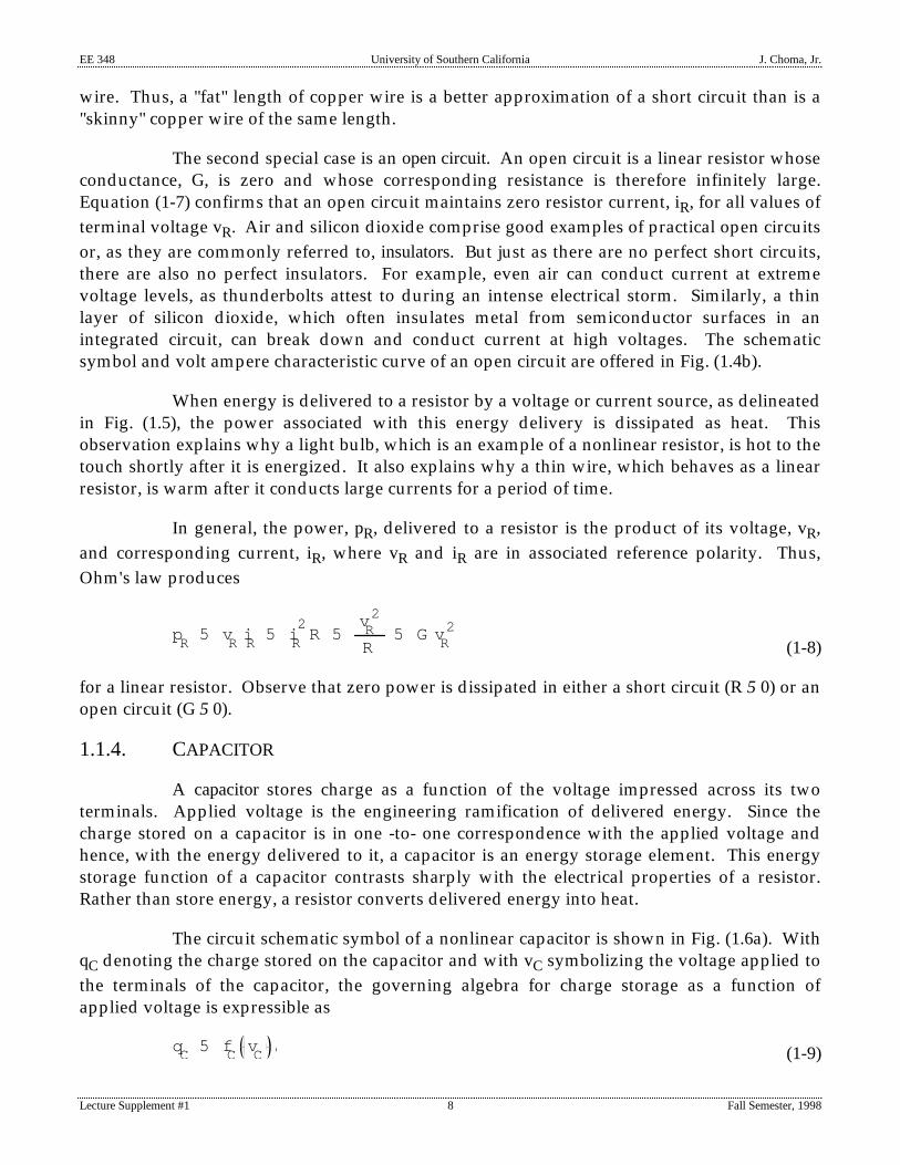
The second special case is an open circuit. An open circuit is a linear resistor whoseconductance, G, is zero and whose corresponding resistance is therefore infinitely large.Equation (1-7) confirms that an open circuit maintains zero resistor current, iR, for all values ofterminal voltage vR. Air and silicon dioxide comprise good examples of practical open circuitsor, as they are commonly referred to, insulators. But just as there are no perfect short circuits,there are also no perfect insulators. For example, even air can conduct current at extremevoltage levels, as thunderbolts attest to during an intense electrical storm. Similarly, a thinlayer of silicon dioxide, which often insulates metal from semiconductor surfaces in anintegrated circuit, can break down and conduct current at high voltages. The schematicsymbol and volt ampere characteristic curve of an open circuit are offered in Fig. (1.4b).
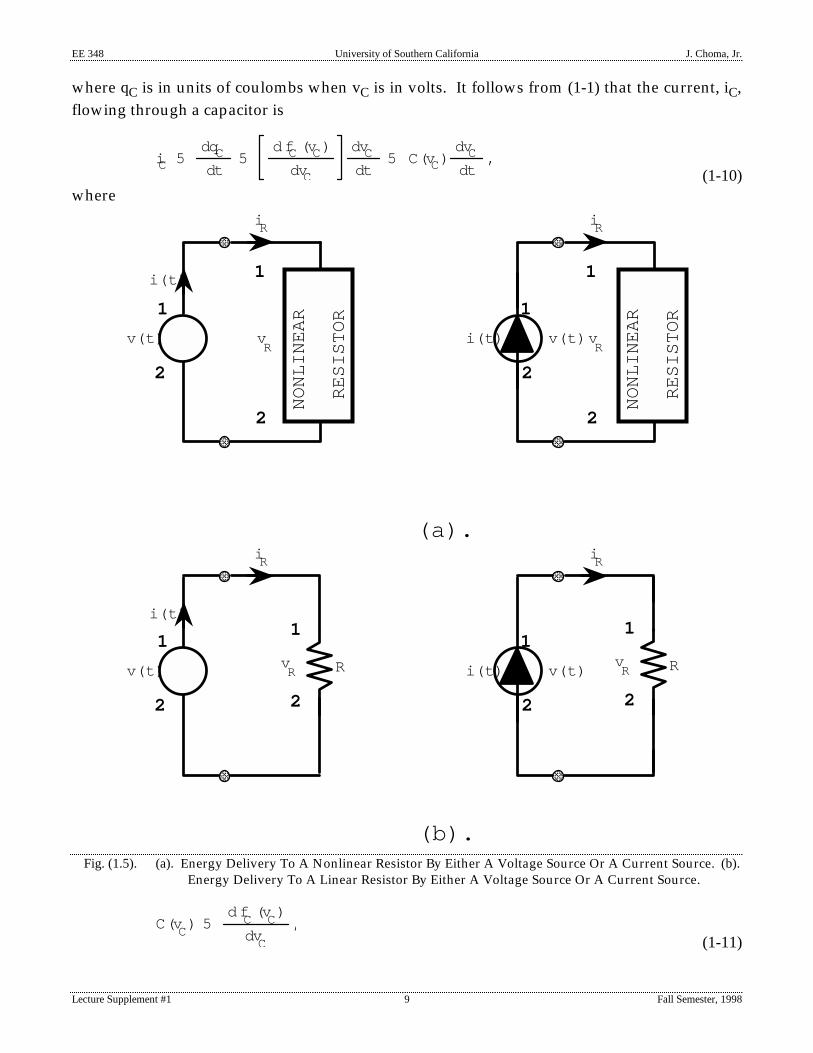
When energy is delivered to a resistor by a voltage or current source, as delineatedin Fig. (1.5), the power associated with this energy delivery is dissipated as heat. Thisobservation explains why a light bulb, which is an example of a nonlinear resistor, is hot to thetouch shortly after it is energized. It also explains why a thin wire, which behaves as a linearresistor, is warm after it conducts large currents for a period of time.
In general, the power, pR, delivered to a resistor is the product of its voltage, vR,and corresponding current, iR, where vR and iR are in associated reference polarity. Thus,Ohm's law produces
pR 5 v
R iR 5 i
R
2 R 5
vR 2
R 5 G v
R 2
(1-8)
for a linear resistor. Observe that zero power is dissipated in either a short circuit (R 5 0) or anopen circuit (G 5 0).
1.1.4. CAPACITOR
A capacitor stores charge as a function of the voltage impressed across its twoterminals. Applied voltage is the engineering ramification of delivered energy. Since thecharge stored on a capacitor is in one -to- one correspondence with the applied voltage andhence, with the energy delivered to it, a capacitor is an energy storage element. This energystorage function of a capacitor contrasts sharply with the electrical properties of a resistor.Rather than store energy, a resistor converts delivered energy into heat.
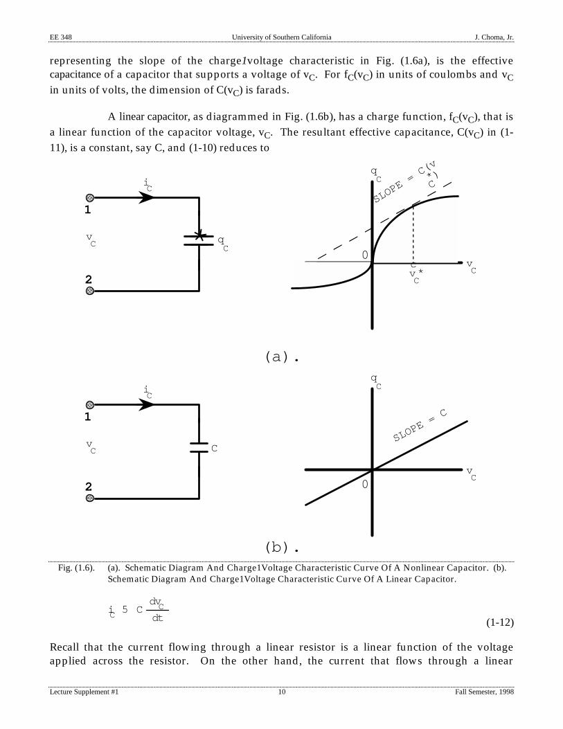
The circuit schematic symbol of a nonlinear capacitor is shown in Fig. (1.6a). WithqC denoting the charge stored on the capacitor and with vC symbolizing the voltage applied tothe terminals of the capacitor, the governing algebra for charge storage as a function ofapplied voltage is expressible as
qC 5 f
C vC , (1-9)
EE 348 University of Southern California J. Choma, Jr.
Lecture Supplement #1 9 Fall Semester, 1998
where qC is in units of coulombs when vC is in volts. It follows from (1-1) that the current, iC,flowing through a capacitor is
iC 5 dqC
dt 5
d fC (vC)
dvC dvC
dt 5 C(vC)
dvC
dt ,
(1-10)where
NONLINEAR
RESISTOR
NONLINEAR
RESISTOR
vR
1
2
iR������
������
������������
i(t)
v(t)
1
2
i(t) v(t)
1
2
vR
1
2����������
����������
iR
(a).
(b).
iR
������������
������������
i(t)
����������
����������
iR
RvR
1
2
v(t)
1
2
i(t) v(t)
1
2
RvR
1
2
Fig. (1.5). (a). Energy Delivery To A Nonlinear Resistor By Either A Voltage Source Or A Current Source. (b).Energy Delivery To A Linear Resistor By Either A Voltage Source Or A Current Source.
C(vC) 5
d fC (vC)
dvC
,(1-11)
EE 348 University of Southern California J. Choma, Jr.
Lecture Supplement #1 10 Fall Semester, 1998
representing the slope of the charge1voltage characteristic in Fig. (1.6a), is the effectivecapacitance of a capacitor that supports a voltage of vC. For fC(vC) in units of coulombs and vC
in units of volts, the dimension of C(vC) is farads.
A linear capacitor, as diagrammed in Fig. (1.6b), has a charge function, fC(vC), that isa linear function of the capacitor voltage, vC. The resultant effective capacitance, C(vC) in (1-11), is a constant, say C, and (1-10) reduces to
iC
vC
1
2����������
����������
(a).
0*
qC
qC
vCv
C*
c
SLOPE = C(v
C)*
iC
vC
1
2����������
�����
(b).
0
qC
vC
CSLOPE = C
Fig. (1.6). (a). Schematic Diagram And Charge1Voltage Characteristic Curve Of A Nonlinear Capacitor. (b).Schematic Diagram And Charge1Voltage Characteristic Curve Of A Linear Capacitor.
iC 5 C
dvC
dt .
(1-12)
Recall that the current flowing through a linear resistor is a linear function of the voltageapplied across the resistor. On the other hand, the current that flows through a linear

EE 348 University of Southern California J. Choma, Jr.
Lecture Supplement #1 11 Fall Semester, 1998
capacitor is proportional to the time rate of change of the voltage applied to the capacitor. Offthe shelf capacitive components having actual volt ampere characteristics that closely reflect(1-12) over wide ranges of voltages and currents are commonly available, especially when thevalue of the capacitance, C, is no larger than a few microfarads (mF).
The linear capacitor is useful in analog active and passive filters and in digitalmemory cells. Ironically, the electrical properties that make capacitors useful in filtering, waveshaping, and information storage applications make them troublesome in others, such as highspeed switching systems and wideband amplifiers. Most of the simultaneously interestingand troublesome characteristics of a linear capacitor stem from the fact that the currentflowing through a capacitor is proportional, not to the value of capacitor voltage, but to thetime rate of change of capacitor voltage. This means, for example, that a large capacitorvoltage that is changing slowly with time incurs relatively small capacitive currents. Indeedconstant voltages –albeit large constant voltages– make a capacitor behave as an open circuit,since (1-12) predicts iC 5 0 for constant vC. On the other hand, a small capacitor voltagechanging rapidly causes large currents to flow through the element.
������������������������������������������������������������������������������������������������������������������������������������������������������������������������������������������������������������������������������������������������������������������������������������������������������������������������������������������������������������������������������������������������������������������������������������������������������������������������������������������������������������������������������������������������������������������������������������������������������������������������������������������������������������������������������������������������������������������������������������������������
������������������������������������������������������������������������������������������������������������������������������������������������������������������������������������������������������������������������������������������������������������������������������
c����������low
frequency
high frequency
low +high frequencies
high frequency
low frequency
ELECTRONIC
SIGNAL
PROCESSOR
L O A D
C
��������������
Fig. (1.7). System Abstraction Of High Frequency Filtering Application Of A Linear Capacitor.
The fact that the current response of a linear capacitor is able to discriminatebetween slowly and rapidly varying input voltages makes it suitable for filtering applications.For example, suppose that a low frequency (slowly changing) input voltage to an electronicsignal processor is contaminated by high frequency (rapidly changing) spurious signals, asabstracted in Fig. (1.7). Consider inserting a capacitor between ground and the node to whichthe signal processor output terminal and a load are incident. The impact of this capacitivefilter is that the output currents generated by the high frequency input spurs are shunted toground, thereby allowing the load to "see" only the currents produced by the low frequencyinput signal voltage that is to be processed. In effect, the capacitor isolates the load from theelectrical effects of high frequency input contaminants.
But the foregoing example can also be used to illustrate an operational disad-vantage. Suppose that the signal processor is to be designed so that both the low and the highfrequency inputs are transmitted uniformly to the load. The capacitor in the diagram of Fig.(1.7) is now an undesirable element in that it inhibits high frequency current conductionthrough the load. The apparent engineering solution to this dilemma is the removal of the

EE 348 University of Southern California J. Choma, Jr.
Lecture Supplement #1 12 Fall Semester, 1998
subject capacitor. Unfortunately, shunt output capacitance is unavoidable. For example, theelectrical nature of a physical load often implies intrinsic charge storage, and hence effectivecapacitance, across its terminals. Moreover, the interconnective wiring between the processoroutput terminal and the load is a potential problem because of the transported mobile chargeassociated with the current conducted by the wire. Since this charge is separated from theground plane by an insulating dielectric (probably air or other type of insulator), theinterconnect itself approximates a shunting capacitance that is continuously distributed alongthe length of the wire[2].
The energy storage nature of a capacitor is likewise both an advantage and adisadvantage, depending on the application addressed. This contention is clarified byinvestigating the energy stored in a linear capacitor. If vC(t) and iC(t) respectively denote thetime domain voltage developed across, and the current flowing through, a linear capacitorhaving capacitance C, the power, pC(t), delivered to the capacitor is
pC(t) 5 v
C(t) i
C(t) 5 C v
C(t)
dvC(t)
dt .
Since the power, pC(t), at time t is the time rate of change of the energy, wC(t),
dwC(t) 5 C v
C(t) dv
C(t) .
An integration of this expression over a time interval of t 5 to –to– any general time t leads to
dwC(x)
wC ( to )
wC ( t )
5 C vC(x) dv
C(x)
vC ( to )
vC ( t )
,
where x is a dummy variable. The resultant energy stored in the capacitor at time t is
wC(t) 5 1 2 C vC
2(t) 5
qC 2(t)
2 C ,
(1-13)
where use has been made of the fact that qC(t) 5 CvC(t) in a linear capacitor.
Equation (1-13) shows that the energy stored in a linear capacitor is in one -to- onecorrespondence with both the voltage applied across the capacitance and the charge storedwithin the element. It follows that arrays of capacitors can be used to store a variety ofinformation, including numerical data and typed text. The only prerequisite underlying thiselectronic storage is that the information identified for archiving be appropriately encoded tovoltages suitable for application across the terminals of the capacitive elements.
In addition to electronic data storage capabilities, linear capacitors can alsoremember stored data. A demonstration of this fact derives from a solution of (1-12) for thecapacitor voltage, vC(t), in terms of the capacitor current, iC(t). To this end,

EE 348 University of Southern California J. Choma, Jr.
Lecture Supplement #1 13 Fall Semester, 1998
dvC (t) 5 1
C iC (t) dt .
Upon integrating from time t 5 0 –to– any general time t,
dvC (x)
vC (to)
vC (t)
5 1 C
iC (x) dx
to
t
,
whence
vC (t) 5 vC
(to) 1 1 C
iC (x) dx
to
t
.
(1-14)
c
1
2
vC(t)
iC(t)
�������������������� ��������
2
1
)o
vC(t
C (charged)
��������������
S1S2
A
B
C
iC(t)
2
1
)o
vC(t
C(not charged
c vC(t)
����������������
t = to
(a). (b).
������������
����������������
D
E
Fig. (1.8). (a). The Charging Of A Linear Capacitor. For Time t , to, Switch S1 Is Connected Between Nodes"A" And "B," And Switch S2 Connects Between Nodes "C" And "D." At Time t 5 to, Switch S1 IsThrown To Connect Node "B" To The Open Circuited Node, Node "E," While Simultaneously,Switch S2 Is Thrown To Connect Node "D" To Node "A." (b). Equivalent Circuit Of The StructureIn (a) For Time t > to.
Equation (1-14) defines, and Fig. (1.8) symbolically overviews, the voltageresponse, vC(t), of a linear capacitor that is energized by a current, iC(t), for time t > to. Unlike aresistor, this voltage response is not exclusively attributed to the applied current. Instead,vC(t) is the superposition of two voltages. The first, vC(to), is the voltage to which the capacitoris charged prior to the application of iC(t), at t 5 to. This initial voltage, which corresponds toan initial charge, qC(to) 5 CvC(to), stored in the capacitor at t 5 to behaves as a battery in that it isa constant voltage, independent of current. If no current is conducted by the capacitor, thesecond term on the right hand side of (1-14) is zero, and the net instantaneous capacitorvoltage is held fast at vC(to) for all time. The second component of the net instantaneouscapacitor voltage is the integral term on the right hand side of (1-14). This term is the voltage
EE 348 University of Southern California J. Choma, Jr.
Lecture Supplement #1 14 Fall Semester, 1998
that appears across the linear capacitor if said capacitor is uncharged at the instant of currentapplication. In the course of responding to the applied current, iC(t), the capacitor therefore"remembers" the voltage ramification of charge stored on the capacitor prior to input currentexcitation. The time length of this memory can be very long, provided that iC(t) is zero or ifiC(t) is very small and/or C is very large.
The final noteworthy property of a linear capacitor is the reluctance of its terminalvoltage to change quickly in the face of rapidly changing, finite currents. This property is acorollary to the memory feature discussed above; that is, a capacitor remembers its initialvoltage immediately after a change in its current flow. It also reflects the fact that capacitorterminal voltage is in one –to– one correspondence with stored charge, which, when subjectedto finite forces, cannot be transported instantly. The inability of a capacitor terminal voltage tochange instantaneously can be confirmed analytically by solving (1-14) for the capacitorvoltage, say vC(to1), immediately after initializing the flow of current, iC(t), through thecapacitor at t 5 to. To this end, let iC(t) be bounded by an amplitude, Im, for to < t < to1; that is|iC(t)| < Im. Then
vC (to1 ) < vC
(to) 1 Im
C to1 2 to .
(1-15)
Since the time difference, (to1 2 to), is infinitesimally small, vC(to1) [ vC(to); that is, the capacitorvoltage immediately after current excitation is identical to the capacitor voltage at the instantof a change in input current.
It is important to emphasize that instantaneous changes in capacitor voltages areprecluded if and only if capacitor currents are finite. A result considerably different fromvC(to1) [ vC(to) is obtained when the current flowing in a linear capacitor is impulsive. Forexample, let the capacitor current, iC(t), be the impulse function,
iC(t) 5 Qm d(t2 to ) , (1-16)
where d(t2to) signifies an impulse applied at time t 5 to, and Qm, a charge quantity, is the areaenclosed by iC(t) in the time domain. Since Qm is a constant and d(t2to) encloses unity area for t. to, (1-14) gives
vC (t) 5 v
C (to) 1
Qm
C .
(1-17)
Equation (1-17) confirms that a capacitor voltage at time t can change instantaneously when animpulse current excites the capacitor. In this case, the impulsive current adds a term, Qm/C, tothe initial voltage, vC(to), established immediately prior to the application of the impulse. Infact, the form of the voltage term generated by the impulse current suggests that the charge,Qm, associated with the input current is transferred directly to the capacitor. This observation

EE 348 University of Southern California J. Choma, Jr.
Lecture Supplement #1 15 Fall Semester, 1998
explains why engineering approximations of impulsive inputs are often used in the laboratoryto investigate the zero input responses, which are the effects of initial conditions, of energystorage networks.
EXAMPLE (1.1)The voltage waveform depicted in Fig. (1.9a) is applied across a 1.2 mF capacitor.Sketch the resultant time domain response of the current flowing through thecapacitance. Assume that the capacitive current flows in associated referencepolarity with the given voltage.
SOLUTION (1.1)From (1-12), the current flowing through the capacitor is directly propor-tional to the time domain slope of the applied voltage signal. The constantof proportionality is the capacitance, C, which is 1.2 mF.
time, t (mSEC)
v (volts)C
Capacitor Voltage,
c
c
cccc
10
0 6 9 15 21 24
time, t (mSEC)
i (mA)C
Capacitor Current,
c
c
cccc
2
0 6 9 15 21 24
c-4
(a).
(b).
Fig. (1.9). (a). Triangular Voltage Waveform Applied To The Linear Capacitor Addressed In EXAMPLE (1.1).(b). Resultant Current Response Of The Voltage Waveform In (a). The Indicated Current Flows InAssociated Reference Polarity With The Applied Voltage.

EE 348 University of Southern California J. Choma, Jr.
Lecture Supplement #1 16 Fall Semester, 1998
(1). For 0 mSEC , t , 6 mSEC, the time domain slope of the voltagewaveform is constant, positive, and equal to 10 V/6 mSEC 5 1.667kV/SEC. The resultant current is therefore constant and equal to Ctimes this slope, or 2 mA.
(2). For 6 mSEC , t , 9 mSEC, the time domain slope of the voltagewaveform is constant, negative, and equal to 210 V/3 mSEC 5 23.333kV/SEC. The resultant current is therefore constant and equal to Ctimes this slope, or 24 mA.
(3). In the time interval, 9 mSEC , t , 15 mSEC, the time domain slope of thevoltage waveform is zero. The resultant current is likewise 0.
(4). The second triangular pulse in the waveform of Fig. (1.9a) replicatesthe first pulse, whose effects have just been studied. Accordingly, theresultant capacitive current, flowing in associated reference polaritywith the applied voltage, is as depicted in Fig. (1.9b).
Note that the effect of the capacitor is to produce a current waveform whosetime domain shape differs considerably from that of the applied voltagesignal. This problem therefore suggests that capacitors have utility in waveshaping applications.
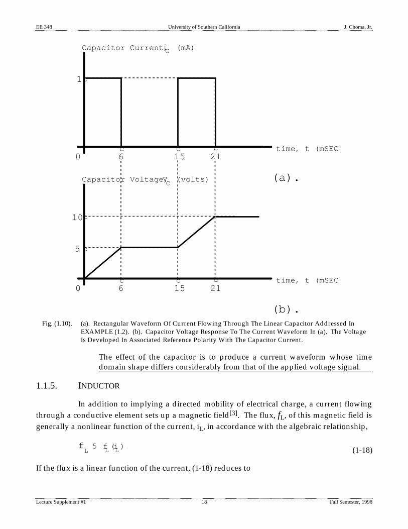
EXAMPLE (1.2)The current waveform depicted in Fig. (1.10a) flows through a 1.2 mF capacitor.Sketch the resultant time domain response of the voltage developed across theterminals of the capacitance, assuming that the capacitor voltage, vC(t), is zero attime t 5 0. Assume that the given current flows in associated reference polarity withthe capacitor voltage.
SOLUTION (1.2)Equation (1-14) is the relevant expression for computing the voltagedeveloped across the terminals of the subject capacitor.
(1). For 0 mSEC < t < 6 mSEC, the current, iC(t), flowing through thecapacitor is a constant value of 1 mA. Since vC(0) is given as zero, thecapacitor voltage in the indicated time interval is
vC (t) 5 1
(1.2)(102 6)
(1)(102 3) dx
0
t
5 t 1.2
,
where t in mSEC delivers vC(t) in volts. Clearly, vC(t) is linear withtime, and vC(6) 5 5 volts.
(2). For 6 mSEC < t < 15 mSEC, zero current flows through the capacitor.

EE 348 University of Southern California J. Choma, Jr.
Lecture Supplement #1 17 Fall Semester, 1998
From (1-14), the five volts to which the capacitor charged during thefirst time interval addressed in the preceding step is resultantlysustained throughout the 6 mSEC -to- 15 mSEC interval; that is vC(t) 5 5
volts.
(3). In the time interval, 15 mSEC < t < 21 mSEC, the capacitor currentreverts to iC(t) 5 1 mA, a constant. Unlike the 0 mSEC -to- 6 mSEC
interval, the capacitor voltage is 5 volts at the start of the second 1 mApulse. Using (1-14) once again, the resultant capacitor voltage for 15mSEC < t < 21 mSEC is
vC (t) 5 5 1
1
(1.2) (1) dx15
t
5 5 1 t 2 15
1.2 ,
where t in mSEC gives vC(t) in volts. Observe that vC(21) 5 10 volts, andsince iC(t) 5 0 for t . 21 mSEC, vC(t) [ 10 volts for all time t . 21 mSEC. Theresultant capacitor voltage, developed in associated reference polaritywith the current flowing through the capacitor, is portrayed in Fig.(1.10b).
EE 348 University of Southern California J. Choma, Jr.
Lecture Supplement #1 18 Fall Semester, 1998
time, t (mSEC)
i (mA)CCapacitor Current,
c
c
cc
1
0 6 15 21
(a).
time, t (mSEC)
v (volts)C
Capacitor Voltage,
c
c
cc
5
0 6 15 21
(b).
c
10
Fig. (1.10). (a). Rectangular Waveform Of Current Flowing Through The Linear Capacitor Addressed InEXAMPLE (1.2). (b). Capacitor Voltage Response To The Current Waveform In (a). The VoltageIs Developed In Associated Reference Polarity With The Capacitor Current.
The effect of the capacitor is to produce a current waveform whose timedomain shape differs considerably from that of the applied voltage signal.
1.1.5. INDUCTOR
In addition to implying a directed mobility of electrical charge, a current flowingthrough a conductive element sets up a magnetic field[3]. The flux, fL, of this magnetic field isgenerally a nonlinear function of the current, iL, in accordance with the algebraic relationship,
fL 5 f
L (iL ) . (1-18)
If the flux is a linear function of the current, (1-18) reduces to

EE 348 University of Southern California J. Choma, Jr.
Lecture Supplement #1 19 Fall Semester, 1998
fL 5 L iL , (1-19)
and the element in question is known as a linear inductor. The parameter, L, in this equation iscalled the inductance of the inductor. With fL in units of webers and iL dimensioned inamperes, L has units of henries.
By Faraday's Law, a time varying current flowing through an inductor induces aninductor terminal voltage that is the time rate of change of magnetic flux. For the linearinductor, whose circuit schematic representation is given in Fig. (1.11), this terminal voltage,say vL, is
iL
vL
����������������
����������������
L
2
1
Fig. (1.11). Circuit Schematic Diagram Of A Linear Inductor.
vL 5
dfL
dt 5 L
diL
dt ,
(1-20)
where voltage vL and current iL are in associated reference polarity. A comparison of (1-20)with (1-12) suggests a volt ampere duality between the capacitor and the inductor; that is, themathematical form of (1-20) is identical to that (1-12), save for an interchange of voltage andcurrent variables. Thus, the electrical properties of an inductor can be inferred from thecorresponding electrical properties of a capacitor.
(1). Energy can be stored by a capacitor in the form of stored charge. Energy can likewisebe stored in the magnetic flux associated with the current flowing in an inductor. Theamount, wL(t), of this stored energy is
wL(t) 5 1
2 L i
L
2(t) 5
fL
2(t)
2 L .
(1-21)
The energy stored in the magnetic flux of a linear inductor is seen to be in one –to– onecorrespondence with both the magnetic flux and the inductor current that establishesthe flux. Inductors can therefore be used as data storage elements, provided that thedata identified for storage is encoded to a current suitable for conduction by aninductor. However, there is no widespread use of inductors as data storage elementsbecause of inherent difficulties associated with the manufacturing of small two terminalcomponents whose electrical characteristics approximate those of linear inductors.

EE 348 University of Southern California J. Choma, Jr.
Lecture Supplement #1 20 Fall Semester, 1998
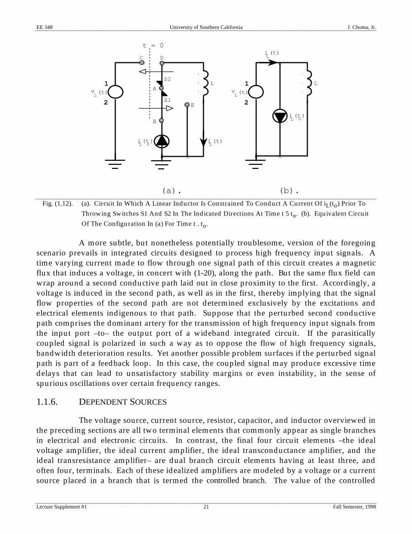
(2). The inductive counterpart to (1-14) is the current relationship,
iL (t) 5 iL (to) 1 1 L vL (x) dxto
t
,
(1-22)
which shows that an inductor "remembers" stored information in the form of an initialcurrent, iL(to). The electrical implication of (1-22) is highlighted by the circuit of Fig.(1.12a). At time t 5 to, switch S1 is thrown to connect node "B" to "E" andsimultaneously, switch S2 is thrown to interconnect nodes "C" and "D." Immediatelybefore time to, S1 connects node "A" to node "B," and S2 interconnects node "A" withnode "D," thereby effecting a current, iL(to), flowing through the inductor of inductancevalue L. When the two switches are thrown at t 5 to, this current initializes the netinstantaneous inductor current, iL(t), for t > to. The result is that the circuit given in Fig.(1.12b) models the circuit in Fig. (1.12a) for t > to.
(3). Recall that the voltage across a capacitor excited by finite current cannot be made tochange instantaneously. For the case of an inductor, current cannot change instan-taneously, as long as the time domain voltage across the terminals of the inductor isfinite. Impulsive inductor terminal voltages do produce instantaneous changes incurrent, just as impulsive currents flowing through capacitors permit instantaneouschanges in capacitor voltages.
Although inductive components are seldom used in microelectronics, they play apivotal role in explaining parasitic coupling phenomena in electronic circuits and systems.Undesirable electrical coupling between two conductive and adjacent circuit paths is often thecause of excessive distortion, electrical interference, and even dynamical instability. Anexample of spurious coupling is the audio and video noise evidenced in a television receiveroperated near a heavy duty power tool. In the absence of sufficient shielding between thetelevision antenna lead in wire and the power cord of the electrical tool, magnetic fieldsprecipitated by the relatively large currents conducted by the tool can envelop, or couple with,the antenna lead in cable. Since appliances are powered by sinusoidal currents, the fluxproduced by the power tool changes with time, thereby inducing voltages along incrementallengths of both the appliance power cord and the antenna cable. The result is that the neteffective signal established across the antenna input terminals of the television receiver is dueto both the transmitted signal received by the antenna and coupled voltages induced by thecurrent that energizes the power tool. The upshot of this undesired coupling is impairedaudio and/or visual reception. To be sure, the magnetic fields of the antenna cable also couplewith those of the power cord of the tool. However, the fields produced by the very smallantenna currents induce proportionately small voltages across incremental lengths of thepower cord of the tool and therefore, they exert an almost immeasurable influence on theelectrical performance of the tool.
EE 348 University of Southern California J. Choma, Jr.
Lecture Supplement #1 21 Fall Semester, 1998
c
S1
1
2
�������
�������
��������������
�������� �������
c
vL(t)
iL(to)
C D
A
B
E
iL(t)
S2
iL(to)
iL(t)
t = 0
c
cc
(a). (b).
1
2
vL(t)
L L
Fig. (1.12). (a). Circuit In Which A Linear Inductor Is Constrained To Conduct A Current Of iL(to) Prior ToThrowing Switches S1 And S2 In The Indicated Directions At Time t 5 to. (b). Equivalent CircuitOf The Configuration In (a) For Time t . to.
A more subtle, but nonetheless potentially troublesome, version of the foregoingscenario prevails in integrated circuits designed to process high frequency input signals. Atime varying current made to flow through one signal path of this circuit creates a magneticflux that induces a voltage, in concert with (1-20), along the path. But the same flux field canwrap around a second conductive path laid out in close proximity to the first. Accordingly, avoltage is induced in the second path, as well as in the first, thereby implying that the signalflow properties of the second path are not determined exclusively by the excitations andelectrical elements indigenous to that path. Suppose that the perturbed second conductivepath comprises the dominant artery for the transmission of high frequency input signals fromthe input port –to– the output port of a wideband integrated circuit. If the parasiticallycoupled signal is polarized in such a way as to oppose the flow of high frequency signals,bandwidth deterioration results. Yet another possible problem surfaces if the perturbed signalpath is part of a feedback loop. In this case, the coupled signal may produce excessive timedelays that can lead to unsatisfactory stability margins or even instability, in the sense ofspurious oscillations over certain frequency ranges.
1.1.6. DEPENDENT SOURCES
The voltage source, current source, resistor, capacitor, and inductor overviewed inthe preceding sections are all two terminal elements that commonly appear as single branchesin electrical and electronic circuits. In contrast, the final four circuit elements –the idealvoltage amplifier, the ideal current amplifier, the ideal transconductance amplifier, and theideal transresistance amplifier– are dual branch circuit elements having at least three, andoften four, terminals. Each of these idealized amplifiers are modeled by a voltage or a currentsource placed in a branch that is termed the controlled branch. The value of the controlled

EE 348 University of Southern California J. Choma, Jr.
Lecture Supplement #1 22 Fall Semester, 1998
voltage or current source is exclusively dependent on a current flowing through, or on avoltage developed across, a second circuit branch that is referred to as the controlling branch.Collectively, the controlled and controlling branches comprise a dependent source. The voltampere characteristics of a dependent voltage or a dependent current source are a first ordercircuit level ramification of complex physical processes taking place in electrical, electronic,mechanical, electro-mechanical, or other types of systems undergoing analysis. The fourdependent sources described below are ideal in the sense that all of these sources lack internalresistances, capacitances, and inductances.
1.1.6.1. IDEAL VOLTAGE AMPLIFIER
An ideal voltage amplifier delivers a voltage across its controlled branch that isproportional to the controlling branch voltage established by independent sources of exci-tation. The dependent source used to model the electrical properties of this type of amplifier isa voltage controlled voltage source (VCVS). Its schematic representation is offered in Fig. (1.13),for which the characteristic volt ampere equations are
i i 5 0
vo 5 m v
i
} .(1-23)
In (1-23), ii is a null input current flowing in the open circuited controlling branch of thesource, vi is the voltage across the controlling branch, vo is the voltage appearing across thecontrolled branch, and m is a voltage amplification factor, or voltage gain. The controlled voltageof a VCVS remains mvi, regardless of any resistive, capacitive, or inductive load placed acrossthe terminals of the controlled branch.
A VCVS is commonly invoked to model the low frequency transfer characteristicsof an operational amplifier (op-amp). The circuit schematic diagram of Fig. (1.14a) portrays anop-amp as a five terminal device. Constant voltages, 1VCC and 2VEE, which are known asbiasing voltages, are applied to two of the five op-amp terminals to achieve nominally linearinput -to- output transfer characteristics. In the schematic diagram, it is understood that thenegative terminal of the 1VCC source lies at ground potential, as does the positive terminal ofthe 2VEE bias supply. Input signal voltages are applied to either or both of the terminalslabeled as (2) and (1), which are respectively referred to as the inverting and the non-invertinginput ports. As a result of applied input signals, a differential voltage, vd, is developed fromthe inverting input terminal -to- the non-inverting input port. In response to the non-zerodifferential input voltage, vd, a single ended output voltage, vo, is generated from the outputterminal of the op-amp -to- ground.
In an ideal operational amplifier, the two input currents, i2 and i1, are zero.Moreover, the relationship of vo to vd is as depicted graphically in Fig. (1.14b). Over the

EE 348 University of Southern California J. Choma, Jr.
Lecture Supplement #1 23 Fall Semester, 1998
���������������������������������������������������������
����������
�����
��������������
�������
vovi
1 1
22
ii
io
m vi
1
2
CONTROLLING BRANCH
CONTROLLED BRANCH
Fig. (1.13). Schematic Diagram Of A Voltage Controlled Voltage Source (VCVS) Used To Model The VoltAmpere Characteristics Of An Ideal Voltage Amplifier.
c2 VEE
i1
1 VCC
����������
����������
������������������
vo
1
������������������2
vd
1
2
2
1
op-amp
i2
vo
vd
2 VEE
1 VCC
0
SLOPE = 2 AOL
c
����������������������������������������������������������������
�������
����������������
�����vo
1
2
1
2
vd
i2
i1
AOL
vd
(a). (b).
(c).
~2!
~1!
Fig. (1.14). (a). Circuit Schematic Symbol Of An Operational Amplifier (Op-Amp). (b).Idealized LowFrequency Transfer Characteristic Of An Op-Amp. (c).VCVS Model Of An Op-Amp OperatedIn The Linear Region Of Its Transfer Characteristic Curve.

EE 348 University of Southern California J. Choma, Jr.
Lecture Supplement #1 24 Fall Semester, 1998
output voltage range, 2VEE < vo < 1VCC, this relationship is linear and expressible as
vo 5 2 AO L vd , (1-24)
where AOL is termed the open loop gain of the op-amp. This simple linear relationship and thefact that i2 5 i1 [ 0 allow the ideal op-amp to be modeled by a VCVS, as shown in Fig. (1.14c). Itis important to note that the VCVS model of an op-amp is valid only for output signal voltageexcursions of 2VEE < vo < 1VCC. From (1-24), this output signal range corresponds to adifferential input signal swing of
2 VCC
AO L < v
d < 1
VEE
AO L .
(1-25)
A practical op-amp, has AOL of the order of tens -to- even hundreds of thousands. Thus, (1-25)imposes severe restrictions on the allowable input signal swing. For example, in an op-amphaving AOL 5 80,000 and biased with VCC 5 VEE 5 12 volts, linearity requires that thedifferential input voltage be restricted to the range, _vd_ < 150 mvolts!
c
R1
C1
kc c������������
R2
C2
ixv
xvo
vi
R1
C1
c c������
R2
C2
vx
vi
��������������������������������������������������������������
�������������� v
o
1
2
kvx
c
(a).
(b).

EE 348 University of Southern California J. Choma, Jr.
Lecture Supplement #1 25 Fall Semester, 1998
Fig. (1.15). (a). Low pass Active RC Filter Incorporating An Amplifier Having A Voltage Gain Of k. (b).Equivalent Circuit Of The Active Filter In (a).
A second example of the use of a VCVS is the analysis of active RC filters. Con-sider the low pass filter of Fig. (1.15a)[4]. This structure uses an amplifier having a voltagegain, k, which means that for a suitable range of input voltages, vx, vo 5 kvx. Assuming that theamplifier draws no input current, (ix 5 0) a useful equivalent circuit of the filter is the VCVS
topology depicted in Fig. (1.15b).
1.1.6.2. IDEAL CURRENT AMPLIFIER
The ideal current amplifier is the dual of the ideal voltage amplifier. Morespecifically, an ideal current amplifier produces a current flowing through its controlledbranch that is proportional to the controlling branch current established by independentsources. The dependent source used to model the electrical properties of a current amplifier isa current controlled current source (CCCS). Its schematic representation in Fig. (1.16), suggestscharacteristic volt ampere equations of the form,
���������������������������������������������������������
����������
����������
��������������
��������������
vovi
1 1
22
ii
io
b ii
CONTROLLING BRANCH
CONTROLLED BRANCH
Fig. (1.16). Schematic Diagram Of A Current Controlled Current Source (CCCS) Used To Model The VoltAmpere Characteristics Of An Ideal Current Amplifier.
v i 5 0
io 5 b i
i
} ,(1-26)
where b is termed the current gain of the CCCS. Note that vi is the null input voltage across thecontrolling branch of the CCCS, ii is the input current flowing through the short circuitedcontrolling branch, and io designates the output current conducted by the controlled branch.The output current remains bii, regardless of the electrical nature of any load connected acrossthe two terminals of the controlled branch.
Under certain operating conditions, a bipolar junction transistor (BJT) behaves as acurrent controlled current source. The BJT is a three terminal device, as indicated by its circuitschematic symbol in Fig. (1.17). These terminals are the collector (C), base (B), and emitter (E).The controlled, or output, current, ic, flows into the collector. To first order, the collector

EE 348 University of Southern California J. Choma, Jr.
Lecture Supplement #1 26 Fall Semester, 1998
current is proportional to the controlling, or input, current, ib, by a factor of a constant, hFE;that is,
ic 5 h
FE ib . (1-27)
������������
�����
����������
ib
ic
B
C
EFig. (1.17). Circuit Schematic Symbol Of A Bipolar Junction Transistor (BJT).
������������������������������������������������������������������������
c
21VE
ib
�����B
�����ic
C
�����E
hFE ib
Fig. (1.18). Approximate Equivalent Circuit Of The Bipolar Junction Transistor.
As is substantiated later in this text, the approximate equivalent circuit of a BJT, which cap-italizes on the CCCS nature of (1-27), is the structure depicted in Fig. (1.18). The battery ofvoltage VE, which appears in series with the base terminal, reflects the electrical impact ofphysical processes intrinsic to the transistor.
1.1.6.3. IDEAL TRANSCONDUCTANCE AMPLIFIER
As is the case with an ideal current amplifier, the controlled variable of an idealtransconductance amplifier is a current that is independent of any electrical load imposedacross the terminals of the controlled branch. But unlike the current amplifier, the controlledcurrent of a transconductance amplifier is linearly proportional to the voltage appearingacross the open circuit terminals of the controlling branch.
The dependent source pertinent to a transconductance amplifier is a voltagecontrolled current source (VCCS). Its schematic representation appears in Fig. (1.19), for whichthe volt ampere relationships are
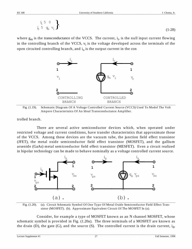
EE 348 University of Southern California J. Choma, Jr.
Lecture Supplement #1 27 Fall Semester, 1998
i i 5 0
io 5 gm v i } ,
(1-28)
where gm is the transconductance of the VCCS. The current, ii, is the null input current flowingin the controlling branch of the VCCS, vi is the voltage developed across the terminals of theopen circuited controlling branch, and io is the output current in the con
���������������������������������������������������������
����������
����������
��������������
��������������
vovi
1 1
22
ii
io
CONTROLLING BRANCH
CONTROLLED BRANCH
vi
gm
Fig. (1.19). Schematic Diagram Of A Voltage Controlled Current Source (VCCS) Used To Model The VoltAmpere Characteristics Of An Ideal Transconductance Amplifier.
trolled branch.
There are several active semiconductor devices which, when operated underrestricted voltage and current conditions, have transfer characteristics that approximate thoseof the VCCS. Among these devices are the vacuum tube, the junction field effect transistor(JFET), the metal oxide semiconductor field effect transistor (MOSFET), and the galliumarsenide (GaAs) metal semiconductor field effect transistor (MESFET). Even a circuit realizedin bipolar technology can be made to behave nominally as a voltage controlled current source.
������������������������������������������������
������
������������
��������
����������
1 1
22�����
����������
������
������������
id
igvds
1
2
vgs
1
2c
gmvgsv
gsvds
id
ig
c
(a). (b).Fig. (1.20). (a). Circuit Schematic Symbol Of One Type Of Metal Oxide Semiconductor Field Effect Tran-
sistor (MOSFET). (b). Approximate Equivalent Circuit Of The MOSFET In (a).
Consider, for example a type of MOSFET known as an N channel MOSFET, whoseschematic symbol is provided in Fig. (1.20a). The three terminals of a MOSFET are known asthe drain (D), the gate (G), and the source (S). The controlled current is the drain current, id,
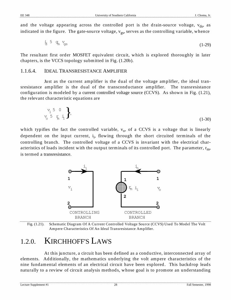
EE 348 University of Southern California J. Choma, Jr.
Lecture Supplement #1 28 Fall Semester, 1998
and the voltage appearing across the controlled port is the drain-source voltage, vds, asindicated in the figure. The gate-source voltage, vgs, serves as the controlling variable, whence
id 5 g
m vgs .
(1-29)
The resultant first order MOSFET equivalent circuit, which is explored thoroughly in laterchapters, is the VCCS topology submitted in Fig. (1.20b).
1.1.6.4. IDEAL TRANSRESISTANCE AMPLIFIER
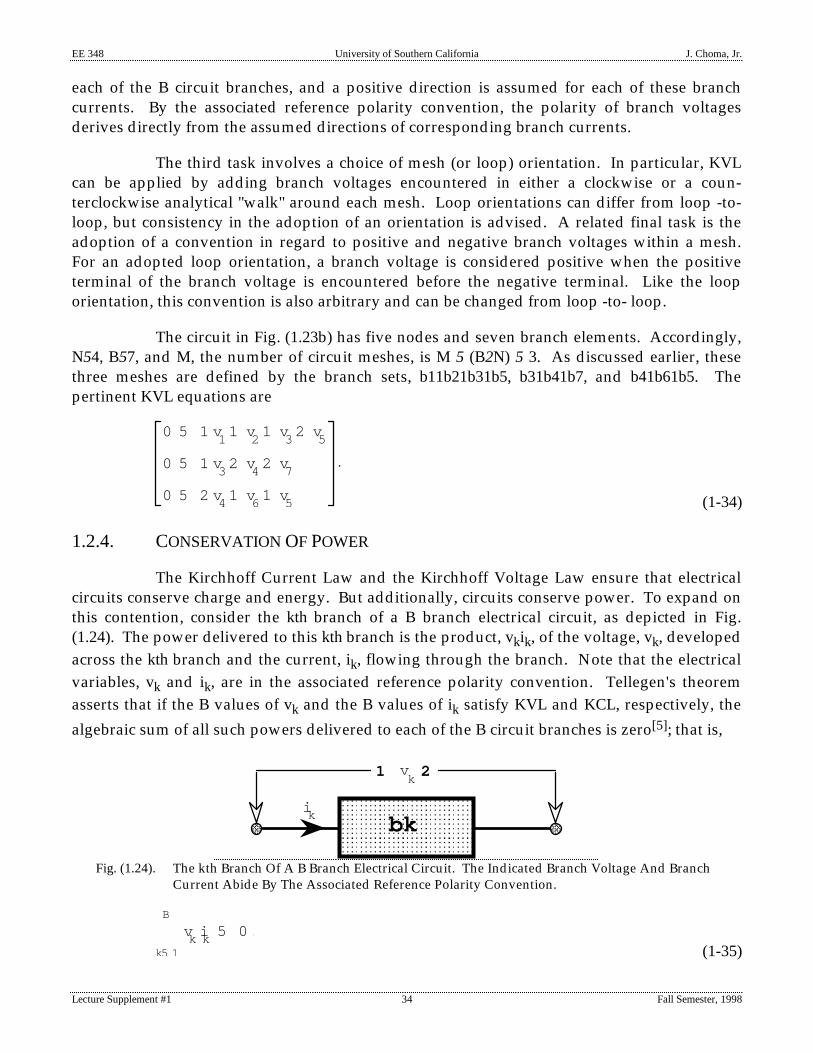
Just as the current amplifier is the dual of the voltage amplifier, the ideal tran-sresistance amplifier is the dual of the transconductance amplifier. The transresistanceconfiguration is modeled by a current controlled voltage source (CCVS). As shown in Fig. (1.21),the relevant characteristic equations are
v i 5 0
vo 5 r
m i i
} ,(1-30)
which typifies the fact the controlled variable, vo, of a CCVS is a voltage that is linearlydependent on the input current, ii, flowing through the short circuited terminals of thecontrolling branch. The controlled voltage of a CCVS is invariant with the electrical char-acteristics of loads incident with the output terminals of its controlled port. The parameter, rm,is termed a transresistance.
���������������������������������������������������������
������������������
�����
��������������
�������
vovi
1 1
22
ii
io
CONTROLLING BRANCH
CONTROLLED BRANCH
iirm
1
2
Fig. (1.21). Schematic Diagram Of A Current Controlled Voltage Source (CCVS) Used To Model The VoltAmpere Characteristics Of An Ideal Transresistance Amplifier.
1.2.0. KIRCHHOFF'S LAWS
At this juncture, a circuit has been defined as a conductive, interconnected array ofelements. Additionally, the mathematics underlying the volt ampere characteristics of thenine fundamental elements of an electrical circuit have been explored. This backdrop leadsnaturally to a review of circuit analysis methods, whose goal is to promote an understanding

EE 348 University of Southern California J. Choma, Jr.
Lecture Supplement #1 29 Fall Semester, 1998
of the interrelationships among the volt ampere characteristics of circuit elements, thetopological structure of the interconnection of these elements, and the resultant input -to-output (I/O) circuit relationships.
Circuit analysis formalizes a set of independent equations whose simultaneoussolution yields the currents flowing through, and the corresponding voltages appearingacross, all circuit elements. The relevant analytical tools are the Kirchhoff Current Law (KCL)and the Kirchhoff Voltage Law (KVL), which are the circuit level ramifications of conservationof charge and conservation of energy, respectively. A systematic application of KCL and KVLto generalized circuit structures requires an understanding of a few concepts related to thetopology of circuits; that is, the interconnective structure of the elements embedded in thecircuit.
1.2.1. TOPOLOGICAL CONCEPTS
The circuit branch is the first of the topological concepts to which the precedingsection of material alludes. A branch of a circuit is any two terminal circuit element. Thus,circuits have independent voltage and current source branches, resistor branches, capacitorbranches, inductor branches, and branches that define the controlling or controlled terminalpairs of any one of the four possible dependent sources. The terms, element and branch, andthe phrases, branch element and circuit branch, as applied to electrical circuits, refer to the samething. The circuit abstracted in Fig. (1.22) displays seven branches, which are labeled b1 -through- b7. Since this circuit is drawn without a delineation of the specific electrical nature ofeach of the seven branches, the circuit displays only the topology of the network.
The interconnection of precisely two branches of a circuit is a junction. On theother hand, the interconnection of two or more circuit branches comprises a circuit node. Ajunction is therefore a special case of a node. The circuit of Fig. (1.22) has five nodes; these arenumbered 0 -through- 4. Only node 1, which interconnects branches b1 and b2, is a junction.
If at least one branch of a circuit is an independent voltage or current source,current can be expected to flow through all circuit branches. Since the true direction in whichthese currents flow is unknown prior to an actual circuit analysis, it is necessary to assume apositive current direction for each and every circuit branch. In general, the polarity directionof B such currents must be assumed for a circuit containing B branches. In associatedreference polarity correspondence to each of the B branch currents in a B branch circuit, thereare B branch voltages. The branch currents and voltages for the circuit of Fig. (1.22) aresymbolized as i1 -through- i7 and v1 -through- v7, respectively. It is important to underscorethe fact that while the choice of the branch current directions in any circuit is arbitrary, theselected polarities of the branch voltages is not vagarious. In particular, once a referencedirection for each branch current is chosen –albeit chosen arbitrarily– the associated referencepolarity convention dictates the polarity of each corresponding branch voltage.

EE 348 University of Southern California J. Choma, Jr.
Lecture Supplement #1 30 Fall Semester, 1998
��������������������������������������������������������������������������������������������������������b1
������������������������������������������������������������������������������������������������b3
����������������������������������������������������������������������������������������������������������������������������������b2
����������������������������������������������������������������������������������������������������b4
�����������������������������������������������������������������������������������������������������������������������������b5
������������������������������������������������������������������������������������������������������������������������b6
������������������������������������������������������������������������������������������������������������������������b7
c
c
c
cc
1
23
0
4
v1
i1
i2
i3
i4
i5
i6
i7
v7 21
v3 21 v
4 12
1
2
v2
1
2
v5
1
2
v6
2
1
Fig. (1.22). A Seven Branch, One Junction, Five Node Circuit. The Arrows, Whose Direction Can Be ChosenArbitrarily, Symbolize Branch Currents. The Indicated Branch Voltages Have Polarities ThatAre Dictated By The Associated Reference Polarity Convention.
A loop of a circuit is a collection of branch elements that collectively comprise aclosed path. Practical circuits have numerous loops. Three loops of the circuit in Fig. (1.22) arethe sequence of branches, b11b21b31b5, b71b61b51b3, and b11b21b31b41b6. A loop isindependent of the assumed positive reference directions of branch currents and voltages, andit is also independent of the branch sequence adopted to define the loop. Thus, the loop,b11b21b31b5, is identical to the loop defined by b51b21b11b3.
A mesh is a special case of a loop in that it is a loop that encloses or encircles nobranch of the circuit. A circuit having B branches and (N11) nodes, has (B2N) meshes. Thenumber, say M, of meshes in the circuit of Fig. (1.22) is three, since the circuit at hand has N54and B57. These meshes are easily identified as the branch sequences, b11b21b31b5, b31b41b7,and b41b61b5.

EE 348 University of Southern California J. Choma, Jr.
Lecture Supplement #1 31 Fall Semester, 1998
����������������������������������������������������������������������������������������������������������������������������������b1
������������������������������������������������������������������������������������������������������������������������b3
����������������������������������������������������������������������������������������������������������������������������������
b2
�����������������������������������������������������������������������������������������������������������������������������b4
�����������������������������������������������������������������������������������������������������������������������������b5
������������������������������������������������������������������������������������������������������������������������b6
������������������������������������������������������������������������������������������������������������������������b7
c
c
c
cc
1
23
0
4
v1
i1
i2
i3
i4
i5
i6
i7
v7 21
v3 21 v
4 12
1
2
v2
1
2
v51
2
v62
1
e1
e2
e3
e4
1
2
1
2
1
2
2
1
(a).
(b).
����������������������������������������������������������������������������������������������������������������������������������b1
������������������������������������������������������������������������������������������������b3
����������������������������������������������������������������������������������������������������������������������������������b2
����������������������������������������������������������������������������������������������������b4
�����������������������������������������������������������������������������������������������������������������������������b5
������������������������������������������������������������������������������������������������������������������������b6
������������������������������������������������������������������������������������������������b7
c
c
c
c
v1
i1
i2
i3
i4
i5
i6
i7
v7 21
v3 21 v
4 12
1
2
v2
1
2
v5
1
2
v6
2
1e1
e2
e3
e4
c
Fig. (1.23). (a). Circuit Of Fig. (1.22) Drawn To Indicate The Four Circuit Node Voltages. (b). SimplifiedVersion Of (a). The Ground Node Is Node 0.

EE 348 University of Southern California J. Choma, Jr.
Lecture Supplement #1 32 Fall Semester, 1998
The node voltages of a circuit are the voltages, measured with respect to a commonreference node, that are developed at each circuit node. In an (N11) node circuit, there are(N11) definable node voltages. But since one circuit node serves as the reference point for allcircuit node voltages, the voltage of the reference node is defined to be zero. There aretherefore only N computable node voltages in an (N11) node circuit. In Fig. (1.23a), thesecomputable voltages are indicated as e1 -through- e4, where node 0 is assumed to be thereference node. The reference node adopted in a circuit analysis problem is indicated by theground symbol, which serves as the reference, or "2" end of each circuit node voltage, asshown in Fig. (1.23b).
1.2.2. KIRCHHOFF CURRENT LAW
The Kirchhoff Current Law (KCL) states that at any time, the algebraic sum ofcurrents at each node of a circuit must be zero. Equivalently, KCL asserts that the net sum ofcurrents that enter a node must be identical to the net sum of currents that leave the samenode. KCL reflects charge conservation principles; that is, charge can neither be destroyed norcreated during its transport across an arbitrary cross section of a conductive element.
The maximum number of independent KCL equations that can be written for an(N11) node, B branch circuit is N. Recall that in an (N11) node circuit, only N node voltages canbe computed. This observation leads to the suspicion that the objective of KCL analysis, ornodal analysis, as it is commonly referred to, is a unique solution for the N computable nodevoltages of an (N11) node circuit.
Four preliminary tasks are conducted, usually by inspection, prior to a systematicapplication of KCL. First, the reference node, the N remaining nodes of an (N11) node circuit,and the B branches of the circuit are identified. Second, branch currents are assignedsymbolically to each of the B circuit branches, and a positive direction is assumed for each ofthese branch currents. Recall that the direction in which positive current flows is arbitrary.But in concert with the associated reference polarity convention, the polarity of branchvoltages derives directly from the assumed directions of corresponding branch currents.
The third preliminary task stems from the fact that the application of KCL involvesan algebraic sum of nodal currents. This means that at each circuit node, a decision must bemade as to whether to view a current entering a node as a positive or a negative variable. If anentering nodal current is viewed as a positive circuit variable, a current leaving the same nodeis necessarily a negative variable, and vice versa. The algebraic sign convention adopted at anode is arbitrary, and it need not be consistent from node -to- node. In other words, currentsperceived as positive quantities when they leave one circuit node can be taken as negativevariables when they leave another circuit node. However, to minimize confusion and toachieve a systematic analytical tack, the algebraic sign convention adopted for currents at aparticular circuit node is uniformly enforced at all nodes.
Finally, since a nodal analysis leading to an independent set of KCL relationshipsrequires that KCL be applied to only N of the (N11) circuit nodes, N specific nodes must beearmarked for KCL analysis. In practice, KCL is not explicitly invoked at the reference or

EE 348 University of Southern California J. Choma, Jr.
Lecture Supplement #1 33 Fall Semester, 1998
ground node of the circuit undergoing analysis.
For the circuit of Fig. (1.23b), KCL, applied at nodes 1 -through- 4 in such a waythat currents leaving a node are viewed as positive electrical variables, yields
node #1: 0 5 2 i1 1 i
2
node #2: 0 5 2 i
2 1 i
3 1 i
7
node #3: 0 5 2 i
3 2 i
4 2 i
5
node #4: 0 5 1 i
4 1 i
6 2 i
7
.
(1-31)
For sake of completeness, a similar nodal analysis at node 0 gives
node #0: 0 5 1 i1 1 i
5 2 i
6 . (1-32)
But this equation is not independent of (1-31) since (1-32) is the negative sum of the four KCLrelationships in (1-31). Actually, any four of the five expressions collectively implicit to (1-31)and (1-32) comprise an independent set of KCL equations. To confirm an earlier contentionthat the algebraic sign convention adopted for the branch currents at a particular circuit nodeneed not be uniformly applied to all circuit nodes, reconsider node 3 in the circuit of Fig.(1.23b). This time, let currents be defined as positive when they enter, as opposed to leave,node 3. Then KCL gives
node #3: 0 5 1 i3 1 i
4 1 i
5 , (1-33)
which is tantamount to multiplying both sides of the third KCL expression in (1-31) by (21).
1.2.3. KIRCHHOFF VOLTAGE LAW
The Kirchhoff Voltage Law (KVL) states that at any time, the algebraic sum ofvoltages around all loops of a circuit must be zero. KVL reflects conservation of energy; thatis, energy can neither be destroyed nor created. Instead, the energy applied to a circuit loopcan only be stored in the electrostatic charge fields of capacitive branch elements, it can bestored in the magnetic flux fields associated with inductor branches, or it can be dissipated asheat in resistive circuit branches.
The maximum number of independent KVL equations that can be written for an(N11) node, B branch circuit is (B2N). Since (B2N) is the number of meshes in an (N11) node, Bbranch circuit, a systematic KVL analysis is accomplished by writing KVL equations for onlycircuit meshes. The objective of KVL analysis, which is otherwise known as loop analysis ormesh analysis, is a unique solution for (B2N) circuit mesh currents.
As in the case of KCL, four simple tasks are conducted in advance of an applica-tion of KVL. First, the reference node, the N remaining nodes of an (N11) node circuit, and theB branches of the circuit are identified. Second, branch currents are assigned symbolically to
EE 348 University of Southern California J. Choma, Jr.
Lecture Supplement #1 34 Fall Semester, 1998
each of the B circuit branches, and a positive direction is assumed for each of these branchcurrents. By the associated reference polarity convention, the polarity of branch voltagesderives directly from the assumed directions of corresponding branch currents.
The third task involves a choice of mesh (or loop) orientation. In particular, KVLcan be applied by adding branch voltages encountered in either a clockwise or a coun-terclockwise analytical "walk" around each mesh. Loop orientations can differ from loop -to-loop, but consistency in the adoption of an orientation is advised. A related final task is theadoption of a convention in regard to positive and negative branch voltages within a mesh.For an adopted loop orientation, a branch voltage is considered positive when the positiveterminal of the branch voltage is encountered before the negative terminal. Like the looporientation, this convention is also arbitrary and can be changed from loop -to- loop.
The circuit in Fig. (1.23b) has five nodes and seven branch elements. Accordingly,N54, B57, and M, the number of circuit meshes, is M 5 (B2N) 5 3. As discussed earlier, thesethree meshes are defined by the branch sets, b11b21b31b5, b31b41b7, and b41b61b5. Thepertinent KVL equations are
0 5 1 v1 1 v
2 1 v
3 2 v
5
0 5 1 v
3 2 v
4 2 v
7
0 5 2 v
4 1 v
6 1 v
5
.
(1-34)
1.2.4. CONSERVATION OF POWER
The Kirchhoff Current Law and the Kirchhoff Voltage Law ensure that electricalcircuits conserve charge and energy. But additionally, circuits conserve power. To expand onthis contention, consider the kth branch of a B branch electrical circuit, as depicted in Fig.(1.24). The power delivered to this kth branch is the product, vkik, of the voltage, vk, developedacross the kth branch and the current, ik, flowing through the branch. Note that the electricalvariables, vk and ik, are in the associated reference polarity convention. Tellegen's theoremasserts that if the B values of vk and the B values of ik satisfy KVL and KCL, respectively, the
algebraic sum of all such powers delivered to each of the B circuit branches is zero[5]; that is,
������������������������������������������������������������������������������������������������������������������������������������������������������������������������������������������������������������������������������������������������������������������������������
bk ���������������
vk
ik
1 2
Fig. (1.24). The kth Branch Of A B Branch Electrical Circuit. The Indicated Branch Voltage And BranchCurrent Abide By The Associated Reference Polarity Convention.
vk ik
k5 1
B
5 0 .(1-35)

EE 348 University of Southern California J. Choma, Jr.
Lecture Supplement #1 35 Fall Semester, 1998
The satisfaction of (1-35) demands that at least one of the product terms, vkik, benegative. Since vkik represents the power delivered to the kth branch, vkik . 0 indicates that theenergy associated with this power is either stored in the kth branch or dissipated by the kthbranch as heat. It follows that, vkik , 0 suggests that the kth branch is generating power orequivalently, the kth branch is delivering energy to the rest of the circuit. If there are S branches,numbered 1 -through- S for convenience, for which vkik , 0 the net power, pin, applied to anelectrical circuit is
pin 5 2 v
k ik
k5 1
S
,(1-36)
where pin is understood to be non-negative. The remaining (B2S) branches are characterizedby vkik . 0, and thus, they either store energy or dissipate power. If pdis designates the (B2S)
term sum for which the delivered branch powers are actually positive,
pdis 5 v
k ik
k5 S1 1
B
.(1-37)
Equations (1-37) and (1-36) reduce (1-35) to
pin 5 p
dis , (1-38)
where both pin and pdis are non-negative power terms.
Equations (1-35) and (1-38) provide a relatively convenient means of checking thecomputational propriety of the branch voltages and branch currents deduced from anapplication of KVL and/or KCL. In particular, computational errors are assured if the vk andik evaluated for all B branches of a given network do not satisfy (1-35). Moreover, (1-35), andparticularly (1-38), are routinely exploited as a first level laboratory test to screen out faultyintegrated circuits. Because limiting the net average power dissipated, pdis, by an electroniccircuit is an important design requirement, the average power consumed by each branchimplicit to the circuit is invariably calculated. By (1-37), the sum of these branch power termsis the net power, pdis, consumed by the entire circuit. But since the branches intrinsic to afabricated integrated circuit are not straightforwardly accessible for test and evaluation, thenet power consumed by the circuit is measured indirectly by measuring the power supplied,pin, to the circuit by requisite sources of external energy. A possible design or manufacturingproblem is indicated whenever the measured pin differs substantially from the calculated pdis.

EE 348 University of Southern California J. Choma, Jr.
Lecture Supplement #1 36 Fall Semester, 1998
EXAMPLE (1.3)Use mesh and nodal analyses to solve for all branch currents and all node voltages inthe circuit given in Fig. (1.25). The parameters of the circuit are as follows:
R1 5 10 V R2 5 100 VR3 5 15 V R2 5 600 VR5 5 2,000 V E 5 12 volts.
c
2
1
R1E
3
R2
R3
R4
R5
E
I1
I1
I2
I3
I12 I
2I22 I
3
cE1
E2
c
Fig. (1.25). Circuit Addressed In EXAMPLE (1.3)
SOLUTION (1.3)The circuit at hand has five resistive branches and one voltage source branchfor a net total of six circuit branches. Aside from ground, there are threeother circuit nodes, whose node voltages (referenced to ground) aresymbolized as E1, E2, and E3. With B 5 6 and (N11) 5 4, the number of circuitmeshes is M 5 3.
(1). Three mesh equations are required to solve an independent set of KVLequations for the circuit. To this end, let the current flowing throughresistor R1 be I1, and let the currents conducted by resistors R3 and R5
be I2 and I3, respectively. An application of KCL to the third nodeindicates that the current flowing through the battery, E, is I1, identicalto the current in R1. Similarly, KCL applied to nodes 1 and 2 gives(I12I2) as the current flowing through R2 and (I22I3) as the currentconducted by R4. These currents are delineated in the circuitschematic diagram of Fig. (1.25).
(2). The three circuit meshes are defined by the branch sequences,E1R11R2, R21R31R4, and R41R5. The corresponding mesh equationsare

EE 348 University of Southern California J. Choma, Jr.
Lecture Supplement #1 37 Fall Semester, 1998
E 5 R1 1 R2 I1 2 R2 I2 ,
0 5 2 R2 I1 1 R2 1 R3 1 R4 I2 2 R4 I3 ,
0 5 2 R4 I2 1 R4 1 R5 I3 . .
These three equations can be solved for I1, I2, and I3, with the resultthat I1 5 129.51 mA, I2 5 22.46 mA, and I3 5 5.18 mA. This solutionexpedites the calculation of all other branch currents, all branchvoltages, and all node voltages. Specifically, the current conducted byR2 is (I12I2) 5 107.05 mA, and the current flowing in R4 is (I22I3) 5 17.28
mA. The voltage at node 1 is
E1 5 R2 I1 2 I2 5 10.71 volts ,
and the voltage developed at node 2 is
E2 5 R4 I2 2 I3 5 10.37 volts .
The voltage at node 3 is, of course, the same as the power supplyvoltage, E; that is
E1 [ E 5 12 volts .
(3). One of the three node voltages, E1, E2, and E3, is known by virtue ofthe fact that the battery voltage, E, elevates node 3 above ground by aconstant voltage whose value is 12 volts. Since the purpose of nodalanalysis is the determination of the circuit node voltages, only twonodal equations need be written. With Gi designating theconductance, Gi 5 1/Ri associated with the general resistance, Ri, KCL
applied to nodes 1 and 2 gives
G1 E 5 G
1 1 G
2 1 G
3 E
1 2 G
3 E2 ,
0 5 2 G
3 E1 1 G
2 1 G
3 1 G
5 E
2 .
A simultaneous solution of these equations delivers results that areidentical to the answers provided by mesh analysis.
(4). Tellegen's theorem offers another check on the propriety of thesolutions documented in STEP #2. To this end, let pRi denote thepower delivered to the resistance, Ri. Since pRi is the product of thevoltage developed across, and the current flowing through, resistanceRi, with the understanding that such voltage and current are in theassociated reference polarity convention,

EE 348 University of Southern California J. Choma, Jr.
Lecture Supplement #1 38 Fall Semester, 1998
pR1 5 E 2 E1 I1 5 167.07 m W ,
pR2 5 E1 I1 2 I2 5 1.147 W ,
pR3 5 E1 2 E2 I2 5 7.636 m W ,
pR4 5 E2 I2 2 I3 5 179.19 m W ,
pR5 5 E2 I3 5 53.72 m W .
The sum of these five delivered branch powers, pdis 5 1.554 watts, is thenet power consumed by the five branch resistive network. This powermust equate to the power, say pE, supplied by the battery of voltage E.Indeed, pE 5 pdis, since
pE 5 E I
1 5 1.554 W .
The fact that pE 5 pdis does not prove that the branch current and nodevoltage solutions computed above are correct. But pE � pdis would haveproven that these solutions are wrong.
EXAMPLE (1.4)Adopt KCL as a means of solving for the node voltages of the circuit in Fig. (1.26).The parameters of the circuit are as follows, where the symbology, "KV" representsthousand of ohms or "kilo ohms":
RS 5 300 V RI 5 2.5 KV RE 5 10 VRC 5 100 V RO 5 12 KV RL 5 5 KVRF 5 6 KV hr 5 0.05 b 5 100VS 5 100 mV.
����������������������������������������������������������������������������
c
VS
1
2
RF
hrVxVx
1
2
��������������������������������������������������������������������
b I
I
RS
RI
RE
RO
RC
RL
1
2cc
c cE6
E1
E2 cE3
E4
E5
Fig. (1.26). Circuit Examined In EXAMPLE (1.4).
SOLUTION (1.4)
EE 348 University of Southern California J. Choma, Jr.
Lecture Supplement #1 39 Fall Semester, 1998
The circuit in Fig. (1.26) has seven nodes, inclusive of the ground node towhich the node voltages, E1, E2, E3, E4, E5, and E6 are referred. The circuit ismore complicated than the structure examined in the preceding exampleowing to the presence of a voltage controlled voltage source (hrVx) and acurrent controlled current source (b I).
(1). The first step in the solution process is the determination of a min-imum set of specific nodes to which KCL must be applied. To this end,note that E1 is already known; that is, E1 5 VS 5 100 mV. Since thepurpose of nodal analysis is the evaluation of all circuit node voltages,the fact that E1 is known a priori means that KCL need not be applied tonode 1.
Note further that E3 is not independent of E4, since by KVL,
E3 5 h
r Vx 1 E
4 .
Thus, KCL need be applied to node 3 or to node 4, but not to bothnodes. While on the subject of relating E3 -to- E4, it is worthwhileremembering that the objective of KCL is to arrive at a set of inde-pendent relationships in terms of the node voltages of the circuit. Thecontrolling voltage, Vx, is not a node voltage. But it is related to thenode voltages, E5 and E4, by the KVL expression,
Vx 5 E5 2 E4 .
It follows that E3 can be related to circuit node voltages alone inaccordance with
E3 5 1 2 hr E4 1 hr E5 .
In similar fashion, the controlling variable, I, of the current controlledcurrent source, bI, is expressible in terms of node voltages byobserving that I flows from left -to- right through RI and is thereforegiven by
I 5 E2 2 E
3
RI
5 GI E
2 2 E
3 ,
where conductance notation is adopted for the resistance, RI.Recalling the expression for the voltage, E3, the controlled current, bI,becomes
b I 5 b GI E2 2 1 2 hr E4 2 hr E5 .

EE 348 University of Southern California J. Choma, Jr.
Lecture Supplement #1 40 Fall Semester, 1998
Since KCL need not be applied at node 1, and given that E3 has beenexpressed in terms of E4 and E5, while b I has been cast in terms of E2,E4, and E5, KCL need be applied only at nodes 2, 4, 5, and 6.
(2). For node 2,
0 5 GS E22 VS 1 GI E22 E3 1 GF E22 E6 .
Observe that in addition to flowing through RI, the current, GI(E22E3),flows through the VCVS, hrVx, and flows into node 4. Thus, at node 4,
GI E22 E3 5 GE E4 2 bI 1 GO E42 E5 .
At nodes 5 and 6, KCL yields
0 5 bI 1 GO E
52 E
4 1 G
C E
52 E
6 ,
0 5 G
L E6 1 G
C E
62 E
5 1 G
F E
62 E
2 .
(3). The variables, I and E3, can be eliminated from the preceding fourequations by using the relationships for bI and E3 derived in STEP #2.The result is a system of four algebraic equations in the four unknownnode voltages, E2, E4, E5, and E6. A simultaneous solution of theresultant system of equations produces
E2 5 2 301.07 m V ,
E4 5 29.61 m V ,
E5 5 2 8.40 V ,
E6 5 2 8.10 V .
Since E2, E5, and E6 are negative voltages, nodes 2, 5, and 6 lie below, notabove, the ground reference potential of zero volts. It should also be notedthat the magnitude of the voltages developed at nodes 5 and 6 is larger thanthe applied source voltage of 100 mV. This amplification of the input sourcevoltage is due to the dependent sources, particularly the CCCS. Thepresence of this controlled source means that the circuit under considerationis actually an electrical model of a more complex network in which a currentamplifier is apparently embedded. The network at hand is, in fact, active(capable of signal amplification), whereas networks divorced of controlledsources are passive and therefore incapable of boosting the amplitudes ofinput voltages or currents.

EE 348 University of Southern California J. Choma, Jr.
Lecture Supplement #1 41 Fall Semester, 1998
1.3.0. CIRCUIT THEOREMS
Of the numerous formal theorems that collectively comprise the circuit theorydiscipline, three are especially important to the study of linear electronic circuits and systems.These three theorems are the superposition theorem, Thévenin's theorem, and Norton's theorem.
1.3.1. SUPERPOSITION
Superposition theory applies to linear circuits and systems in which more than onesource of independent energy is applied to produce measurable or computable responses. Thesources of energy, which can be currents or voltages, are called the inputs to the circuit orsystem undergoing study. In electrical circuits, the responses are branch currents, branchvoltages, or node voltages and are called the outputs. Superposition theory states that eachresponse of a linear circuit or system can be determined as the sum of the responses generatedby each independent energy source acting alone[6]. This is to say that the observable responseof a linear circuit or system excited by N sources of energy is the superposition of the responsesof each of the N sources taken one at a time.
Superposition phenomena is commonplace in all practical electrical and electroniccircuits. Consider, for example, a compact disc (CD) played on a CD player that is connectedto a stereo system. If the recorded music consists of a vocalist, a guitarist, and a pianist, it isnatural to expect to hear vocal singing, guitar music, and the sounds of a piano at the speaker,or output, of the stereo system. If any one of the three sources of musical sound does notemanate from the speaker, the stereo system is considered inferior in the sense of its apparentinability to reproduce recorded information faithfully. In effect, superposition with respect tothe various input sources of recorded information is expected –indeed demanded– of a qualitystereo system.
Unfortunately, superposition phenomena can often impact electronic systemsdeleteriously. In the stereo system hypothesized above, improperly shielded and inordinatelylong interconnects between the CD player and the stereo preamplifier are vulnerable toelectromagnetically coupled spurious signals. Thus, audio frequency signals from proximatefluorescent lights or nearby appliances can couple parasitically to the preamplifier. The resultis a net speaker response reflecting a superposition of the desired recorded music and theundesired signal spurs.
Superposition underlies the complete solution to the nth order, linear, ordinarydifferential equation that interrelates the time domain response and inputs of an nth order,linear circuit having distinguishable nodes and branches. Mathematics courses teach that thecomplete time domain solution of this form of an I/O relationship is the sum of thehomogeneous and particular solutions. In the jargon of electrical engineering, the homogeneoussolution is more commonly known as the zero input response or natural response, and theparticular solution is called the zero state response or the forced response. The zero input response,say yzi(t), is found by setting all sources of independent energy applied to the circuitundergoing study, and thus the net effective forcing function, f(t), of the differential equation, to

EE 348 University of Southern California J. Choma, Jr.
Lecture Supplement #1 42 Fall Semester, 1998
zero. On the other hand, the zero state response, yzs(t), accounts for only the specific timedomain nature of the inputs to the circuit or system undergoing study. Thus, the completetime domain solution, say y(t), to the differential I/O equation of an nth order linear circuit is
y(t) 5 yzi(t) 1 y
zs(t) . (1-39)
The scenario just described is more than a mere set of rules for solving a differ-ential equation; it is, in fact, a consequence of superposition theory. To understand thiscontention, recall that of the nine basic elements that can be embedded in a linear circuit, onlythe capacitor and the inductor have volt ampere characteristics in which derivatives of branchvariables appear. Thus, the I/O relationship of a linear circuit is a differential equation onlybecause some of the branch elements of the circuit are capacitors or inductors. But capacitorsand inductors are energy storage elements. This fact implies that the net response, at anygeneral time t, of a linear circuit containing energy storage elements is attributed to twophenomena. The first of these phenomena is the obvious one; namely, the actual input orinputs applied to the circuit drive the circuit response to a certain value. The second derivesfrom the fact that at time t, each capacitor remembers its voltage immediately prior to time tand similarly, each inductor remembers its initialized current. The electrical ramifications ofthese initialized states are energy sources that are manifested in a voltage in the case of acapacitor and a current in the case of an inductor. Like the actual input or inputs to a linearcircuit, these capacitor voltages and inductor currents contribute to the net circuit response attime t. The zero input response, which determines circuit output in the presence of zeroapplied inputs, is a measure of the impact exerted on circuit response by initial capacitorvoltages and initial inductor currents. In contrast, the zero state response quantifies the netoutput response due to the actual inputs applied to the circuit. The individual evaluation ofthese two forms of circuit responses, followed by their summation, as per (1-39), to ascertainthe net circuit response, is a direct exploitation of superposition theory.
EXAMPLE (1.5)Three signal sources, VST, VSN, and ISN, are applied to the circuit shown in Fig.(1.27a). Use superposition theory to determine the net output voltage response, V01.[The output voltage, V02, is used in an assigned problem at the conclusion of thischapter.]
SOLUTION (1.5)The circuit in Fig. (1.27a) can be analyzed straightforwardly through a directapplication of KCL and KVL. The results obtained are identical to those thatderive by superimposing the individual effects of VST, VSN, and ISN.
(1). Fig. (1.27b) is the equivalent circuit pertinent to computing the con-stituent output, Vvst, generated solely by the signal source, VST. Notethat the voltage source, VSN is removed by replacing VSN with a shortcircuit, while the current source, ISN, is removed by supplanting it withan open circuit. By KCL, the current flowing through the resistance,

EE 348 University of Southern California J. Choma, Jr.
Lecture Supplement #1 43 Fall Semester, 1998
RE, is (b11)I. Then, KVL gives
I 5 VST
RS 1 R 1 b1 1 RE .
Since KVL also produces
Vvst 5 2 b R
L I ,
it follows that
Vvst 5 2
b RL VST
RS 1 R 1 b1 1 R
E
is the contribution to the net response spawned exclusively by VST.

EE 348 University of Southern California J. Choma, Jr.
Lecture Supplement #1 44 Fall Semester, 1998
���������������������������������������������������
c
V01
VST
1
2
RS
R
Ib I
1
2
VSN
ISN
RL
����������
V02
������������������
c
cc���������������������������������������������������
c
Vvst
VST
1
2
RS
R
Ib I R
L
�����c
RE
RE
c
����������������������������������������������������������������
c
Vvsn
RS
R
Ib I R
L
�����c
RE
1
2
VSN
����������������������������������������������������������������
c
RS
R
Ib I
RE
ISN
RL
�����
c
cc Visn
(a). (b).
(c). (d).
Ib1 1)(
Ib1 1)(
Ib1 1)(
Fig. (1.27). (a). Circuit Studied In EXAMPLE (1.5) To Demonstrate The Utility Of Superposition. (b).Equivalent Circuit For Computing The Output Due Only To The Voltage, VST. (c). EquivalentCircuit For Computing The Output Due Only To The Voltage, VSN. (d). Equivalent Circuit ForComputing The Output Due Only To The Current, ISN.
(2). Fig. (1.27c) is the equivalent circuit for computing the output, Vvsn, duesolely to the signal source, VSN. Note that the voltage source, VST, andthe current source, ISN, are set to zero. The voltage, Vvsn, is easilyshown to be

EE 348 University of Southern California J. Choma, Jr.
Lecture Supplement #1 45 Fall Semester, 1998
Vvsn 5 1 b RL VSN
RS 1 R 1 b1 1 RE .
(3). Fig. (1.27d) is the equivalent circuit for computing the output, Visn,attributed to the independent current source, ISN. Both of the voltagesources, VST and VSN, are now set to zero. The resultant voltage, Visn,is
Visn 5 1 R
L ISN
.
(4). By superposition theory, the net response is
V01 5 V
vst 1 V
vsn 1 V
isn .
Letting
Gm e D b
RS 1 R 1 b1 1 R
E ,
the substitution of the results for Vvst, Vvsn, and Visn into the equationfor V01 produces
V01 5 2 G
m e RL V
ST 2 V
SN 2
ISN
Gm e .
One advantage of using superposition theory to arrive at the response of acircuit excited by several sources of independent energy is that it inherentlyisolates the individual effects of the applied sources. In the precedingexample, superposition underscores the fact that the voltage sources, VST
and VSN, have an equal magnitude, but opposite algebraic sign, effect on thenet response, V01. Moreover, for a large effective transconductance, Gme, theimpact on V01 of the current source, ISN, is negligible in comparison to themagnitude of the effects exerted by VST and VSN.
1.3.2. THÉVENIN AND NORTON THEOREMS
Circuit analyses frequently entail calculations of either voltages developed across,or currents flowing through, a branch element for various values of the branch element oreven for different types of branch elements. Obviously these calculations can be performed byanalyzing the circuit in which the subject branch is embedded for each and every branchelement of interest. Such a computational tack can be tedious and inefficient. It is tedious ifthe complete analysis of the circuit at hand requires the simultaneous solution of more thanthree equations, and it is inefficient if circuit branch variables other than those associated withthe subject variable element are of no interest. For the case in which the variable branchelement is driven by a linear circuit, Thévenin's theorem and its companion, Norton's theorem,

EE 348 University of Southern California J. Choma, Jr.
Lecture Supplement #1 46 Fall Semester, 1998
provide a useful and insightful alternative to the computational tedium entailed by repetitivecircuit analyses.

EE 348 University of Southern California J. Choma, Jr.
Lecture Supplement #1 47 Fall Semester, 1998
1.3.2.1. THÉVENIN'S THEOREM
Thévenin's theorem states that two terminals of any linear circuit can be modeled by avoltage source in series with a resistance. The voltage source appearing in the Thévenin equivalentcircuit with respect to the two terminals of interest is called the Thévenin voltage, Vth, and theresistance, say Rth, is termed the Thévenin resistance. If the two terminals of interest areextracted from a memoryless circuit, Vth and Rth are constants. On the other hand, a circuitcontaining capacitors and/or inductors produces Vth and Rth that are functions of thefrequencies of the voltage and current signals applied to the circuit. In this case, Vth and Rth
are cast as functions of transformed frequency variables and are respectively referred to as thetransform of the Thévenin voltage and the Thévenin impedance.
������������������������������������������������������������������������������������������������������������������������������������������������������������������������������������������������������������������������������������������������������������������������������������������������������������������������������������������������������������������������������������������������������������������������������������������������������������������������������������������������������������������������������������������������������������������������������������������������������������������������������������������������������������������������������������������������������������������������������������������������������������������������������������������������������������������������������������������������������������������������������������������������������������������������������������������������������������������������������������������������������������������������������������������������������������������������������������������������������������������������������������������������������������������������������������������������������������������������������������������������������������������������������������������������������������������������������������������������������������������������������������������������������������������������������������������������������������������������������������������������������������������������������������������������������������������������������������������������������������������������������������������������������������������������������������������������������������������������������������������������������������������������������������������������������
����������������������������������������������������������������������������������������������������������������������������������������������������������������������������������������������������������������������������������������������������������������������������������������
���������������������������������������������������������������������������������������������������������������������������������������������������������������������������������������������������������������������������������������������������������������������������������������������������������������������������������������������������������������������������������������������������������������������������������������������������������������������������������������������������������������������������������������������������������������������������������������������������������������������������������������������������������������������������������������������������������������������������������������������������������������������������������������������������������������������������������������������������������������������������������������������������������������������������������������������������������������������������������������������������������������������������������������������������������������������������������������������������������������������������������������������������������������������������������������������������������������������������������
����������������
�������
(a).
VL
1
2
IL
L O A D
ENERGIZED
LINEAR
CIRCUIT
B
A
2
1Vth
����������������������������������������������������������������������������������������������������������������������������������������������������������������������������������������������������������������������������������������������������������������������������������������
����������������
�������
VL
1
2
IL
L O A D
B
ARth
(b).
THEVENIN EQUIVALENT CIRCUIT
Fig. (1.28). (a). Diagram Showing A Particular Branch Of An Energized Linear Circuit. (b). SchematicDiagram Of The Thévenin Equivalent Circuit With Respect To Terminals "A" And "B" In The
EE 348 University of Southern California J. Choma, Jr.
Lecture Supplement #1 48 Fall Semester, 1998
Diagram Of (a).
The essence of Thévenin's theorem is illustrated by Fig. (1.28). In Fig. (1.28a), alinear circuit energized by voltage and/or current sources drives a presumably variablebranch that is designated as a general load. The load, which need not have linear volt amperecharacteristics, is connected between nodes "A" and "B" of the circuit. The circuit establishes avoltage, VL, across the load and sustains a current, IL, flowing through the load, as indicated.Regardless of the number of branches and nodes that collectively define the topology of theenergized linear circuit, Thévenin's theorem allows for its replacement by the simple twobranch equivalent circuit of Fig. (1.28b). The two branch Thévenin equivalent circuit is notlikely to be topologically identical to the original structure. It is therefore important tounderstand that the configuration in Fig. (1.28b) is, in general, "equivalent" to that of Fig.(1.28a) only insofar as terminals "A" and "B" are concerned. Specifically, both networks in Fig.(1.28) produce the same load voltage, VL, from terminal "A" -to- terminal "B," and the sameload current, IL, flowing from terminal "A" -to- terminal "B."
The scenario for determining Vth and Rth for the energized linear circuit is a directexploitation of the Thévenin concept. In particular, the model drawn in Fig. (1.28b) is valid forany and all loads connected to terminals "A" and "B." Consider the case in which the load is atest current source, say Ix, as depicted in Fig. (1.29a). In a circuit theoretic sense, this current,which results in a voltage, say Vx, across the subject terminals, can have any arbitrary value.But if the test source is utilized in the laboratory to measure Vth and Rth, Ix must be sufficientlysmall to ensure that the linearity properties of the energized circuit are not compromised.
Recalling Fig. (1.28b), the equivalent circuit with respect to terminals "A" and "B "of the structure in Fig. (1.29a) is as offered in Fig. (1.29b). KVL yields
Vx 5 V
th 1 R
th Ix , (1-40)
which suggests that Vx [ Vth when Ix 5 0. But Ix 5 0 reflects an open circuited load termination.In turn, the corresponding voltage developed from terminal "A" -to- terminal "B," under thecase of an open circuit (or no load) across this terminal pair is the desired Thévenin voltagefrom terminal "A" -to- terminal "B" of the energized linear circuit, as illustrated in Fig. (1.29c).
Equation (1-40) also underscores the fact that Rth is the ratio of Vx -to- Ix when Vth
[ 0. Now, Vth is the open circuit terminal voltage identified in Fig. (1.29c). Since this terminalvoltage is produced exclusively by an energized linear circuit, Vth is the superposition of theeffects of all independent voltage and current sources applied to the circuit undergoingexamination. Thus, if these sources of independent energy are all set to zero, Vth necessarilyreduces to zero. The result is the Thévenin equivalent circuit of Fig. (1.29d), for which Ohm'slaw delivers
Rth 5 Vx
Ix .
(1-41)

EE 348 University of Southern California J. Choma, Jr.
Lecture Supplement #1 49 Fall Semester, 1998
��������������������������������������������������������������������������������������������������������������������������������������������������������������������������������������������������������������������������������������������������������������������������������������������������������������������������������������������������������������������������������������������������������������������������������������������������������������������������������
(a).
Vx
1
2
Ix
ENERGIZED
LINEAR
CIRCUIT
B
A
2
1Vth
Rth
����������
����������
Vx
1
2
Ix
A
������������
������������
(b).
������������������������������������������������������������������������������������������������������������������������������������������������������������������������������������������������������������������������������������������������������������������������������������������������������������������������������������������������������������������������������������������������������������������������������������������������������������������������������������������������������������������������������������������
(c).
1
2
ENERGIZED
LINEAR
CIRCUIT
A
����������
����������
B
B
Vth
B
Rth
Vx
1
2
Ix
A
������������
������
(d).
V th 5 0
5 0Ix
Fig. (1.29). (a). Application Of A Test Current, Ix, From Terminal "B" -To- Terminal "A" Of An EnergizedLinear Circuit. (b). Thévenin Equivalent Circuit, With Respect To Terminals "A" And "B," Of TheNetwork In (a). (c). The Circuit Of (a), But With Ix Set To Zero. The Resultant Open CircuitVoltage From Terminal "A" -To- Terminal "B" Is The Thévenin Voltage, Vth. (d). ThéveninEquivalent Circuit, With Respect To Terminals "A" And "B," Of The Network In (a), But With AllSources Of Independent Energy Set To Zero.
EXAMPLE (1.6)Find the Thévenin equivalent circuit that drives the resistance, RO, in the circuitgiven in Fig. (1.30). Use this model to determine the voltage, VO, for RO 5 100 V,10 KV, and 100 KV. The other branch elements in the circuit are:
R 5 1.5 KV RL 5 5 KVRE 5 5 V b 5 100 VS 5 10 mV.
SOLUTION (1.6)The Thévenin equivalent circuit contains two branch elements. One of theseis a generator representing the Thévenin voltage, Vth, at the terminals ofinterest, and the other is Thévenin resistance, Rth, facing the load that isconnected across the subject terminals.
(1). Fig. (1.30b) is the circuit pertinent to the computation of Vth. Note thatthe load, which is the resistance, RO, in this case, has been supplanted
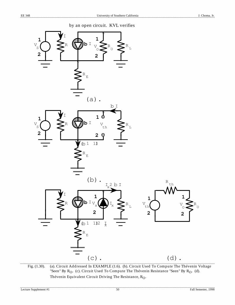
EE 348 University of Southern California J. Choma, Jr.
Lecture Supplement #1 50 Fall Semester, 1998
by an open circuit. KVL verifies
��������������������������������������������������������������������
c
VS
1
2
R
I
b I RO
VO
1
2
RL
RE
c
��������������������������������������������������������������������
c
VS
1
2
R b I Vth
1
2
RL
RE
c
������
������������
��������������������������������������������������������������������
c
R b I RL
RE
c
Vx
Ix
1
2
(a).
(b).
(c).
I
I
b I 1 1)(
b I 1 1)( 2 Ix
b I
b I 2 Ix
1
2
Rth
RO
VO
1
2
Vth
(d).Fig. (1.30). (a). Circuit Addressed In EXAMPLE (1.6). (b). Circuit Used To Compute The Thévenin Voltage
"Seen" By RO. (c). Circuit Used To Compute The Thévenin Resistance "Seen" By RO. (d).
Thévenin Equivalent Circuit Driving The Resistance, RO.

EE 348 University of Southern California J. Choma, Jr.
Lecture Supplement #1 51 Fall Semester, 1998
VS 5 R 1 b1 1 RE I ,
Vth 5 2 b RL I 2 b1 1 RE I ,
whence,
Vth 5 2 b RL 1 b1 1 RE R 1 b1 1 RE
VS .
The numerical answer yielded by this expression is Vth 5 22.50 volts.
(2). Two procedural steps precede the computation of the Théveninresistance, Rth. First, all independent sources in the circuit of Fig.(1.30a) are clamped to zero. In the present example, only one suchsource, VS, is present. Second, the subject load, which here is theresistance, RO, is replaced by a test current source, Ix. The immediateeffect of this current source is to establish a voltage, Vx, in disas-sociated reference polarity with Ix, across its terminals. The resultantequivalent circuit used to calculate Rth is the structure provided in Fig.(1.30c). An analysis of this circuit gives
0 5 R 1 b1 1 RE I 2 R
E Ix ,
Vx 5 R
L I
x2 bI 1 R
E I
x2 b1 1 I .
A solution of the first of these two equations for the current, I, fol-lowed by the substitution of this result into the second equation, leadsto a relationship for which the ratio, Vx/Ix, which is the desiredThévenin resistance, can be cast exclusively in terms of the branchelement parameters of the original network. Following algebraicmanipulation, the result is
Rth [
Vx
Ix 5 R
L
R 1 RE
R 1 b1 1 RE 1 R
E | R
b1 1 ,
where "|" denotes in parallel with. Numerically, Rth 5 3,757 ohms.
(3). Fig. (1.30d) is the Thévenin equivalent circuit that drives the resistance,RO. This simple model gives
VO 5
RO
RO1 R
th V
th .
For RO 5 100 V, VO 5 264.7 mV, while RO 5 10 KV delivers VO 5 21.82 V.Finally, RO 5 100 KV delivers VO 5 22.41 V.

EE 348 University of Southern California J. Choma, Jr.
Lecture Supplement #1 52 Fall Semester, 1998
Observe that the final results follow forthwith from the voltage dividerexpression that relates the desired voltage to the Thévenin voltage andThévenin resistance in the pertinent Thévenin equivalent circuit. Thetradeoff for this trivial computation is the need to analyze two circuits: oneappropriate to the computation of Vth and the other appropriate to thecalculation of Rth. Generally, but not always, this tradeoff is more easilyexpedited than is a repetitive analysis of the entire circuit to which thevariable load is connected.
1.3.2.2. NORTON'S THEOREM
When the Thévenin resistance associated with a terminal pair of an energizedlinear circuit is very large, it may prove difficult or even impossible to compute or measure theThévenin voltage. In these cases, Norton's theorem offers a pragmatic alternative to Thévenin'stheorem. Norton's theorem states that two terminals of any linear circuit are electrically equivalent to acurrent source in shunt with a resistance. The current source appearing in the Norton equivalentcircuit with respect to the two terminals of interest is called the Norton current, Ino. The shuntingresistance is identical to the Thévenin resistance.
Fig. (1.31b) overviews the Norton equivalent circuit at terminals "A" and "B" of thegeneralized circuit abstracted in Fig. (1.28a), which is repeated in Fig. (1.31a) for convenience.Insofar as load variables VL and IL are concerned, the model of Fig. (1.31b) is equivalent to thecircuit of Fig. (1.31a), Moreover, since the Thévenin circuit of Fig. (1.29b) is also equivalent toFig. (1.31a), with respect to predicting the load voltage and current, the Norton and Théveninequivalent circuits must be identical with respect to a mathematical emulation of theobservable electrical characteristics at terminals "A" and "B."
The foregoing observation implies a relationship between the Norton equivalentcurrent, Ino, and the Thévenin equivalent voltage, Vth. It also allows for a physicalinterpretation of the Norton current. To investigate these contentions, consider the network ofFig. (1.31a) for the case of a short circuit load imposed between terminals "A" and "B." Thecurrent conducted by the short circuit is designated Isc. This situation is shown in Fig. (1.32a),while Figs. (1.32b) and (1.32c) give the relevant Thévenin and Norton equivalent circuits,respectively. Since the short circuit constrains the voltage between terminals "A" and "B" tozero, Fig. (1.32b) verifies that
Isc 5 Vth
Rth .
(1-42)
In Fig. (132c), no current can flow through the shunting Thévenin resistance and thus,
Isc [ I
no ; (1-43)
that is, the Norton equivalent current is the current that flows in a short circuited loadinterconnected between terminals "A" and "B" of the energized network of Fig. (1.31a).

EE 348 University of Southern California J. Choma, Jr.
Lecture Supplement #1 53 Fall Semester, 1998
Equations (1-42) and (1-43) combine to deliver
������������������������������������������������������������������������������������������������������������������������������������������������������������������������������������������������������������������������������������������������������������������������������������������������������������������������������������������������������������������������������������������������������������������������������������������������������������������������������������������������������������������������������������������������������������������������������������������������������������������������������������������������������������������������������������������������������������������������������������������������������������������������������������������������������������������������������������������������������������������������������������������������������������������������������������������������������������������������������������������������������������������������������������������������������������������������������������������������������������������������������������������������������������������������������������������������������������������������������������������������������������������������������������������������������������������������������������������������������������������������������������������������������������������������������������������������������������������������������������������������������������������������������������������������������������������������������������������������������������������������������������������������������������������������������������������������������������������������������������������������������������������������������������������������������
��������������������������������������������������������������������������������������������������������������������������������������������������������������������������������������������������������������������������������������������������������������������������������������������������������������������
���������������������������������������������������������������������������������������������������������������������������������������������������������������������������������������������������������������������������������������������������������������������������������������������������������������������������������������������������������������������������������������������������������������������������������������������������������������������������������������������������������������������������������������������������������������������������������������������������������������������������������������������������������������������������������������������������������������������������������������������������������������������������������������������������������������������������������������������������������������������������������������������������������������������������������������������������������������������������������������������������������������������������������������������������������������������������������������������������������������������������������������������������������������������������������������������������������������������������������
��������
��������������
(a).
VL
1
2
IL
L O A D
ENERGIZED
LINEAR
CIRCUIT
B
A
Ino
����������������������������������������������������������������������������������������������������������������������������������������������������������������������������������������������������������������������������������������������������������������������������������������������������������������������������
��������
��������������
VL
1
2
IL
L O A D
B
A
Rth
(b).
NORTON EQUIVALENT CIRCUIT
c
c
Fig. (1.31). (a). Diagram Showing A Particular Branch Of An Energized Linear Circuit. (b). SchematicDiagram Of The Norton Equivalent Circuit With Respect To Terminals "A" And "B" In TheDiagram Of (a).
Vth 5 R
th Ino , (1-44)
which is the previously conjectured relationship between the Thévenin voltage and the Nortoncurrent.

EE 348 University of Southern California J. Choma, Jr.
Lecture Supplement #1 54 Fall Semester, 1998
v
���������������������������������������������������������������������������������������������������������������������������������������������������������������������������������������������������������������������������������������������������������������������������������������������������������������������������������������������������������������������������������������������������������������������������������������������������������������������������������������������������������������������������������������������������
(a).
Isc
1
2
ENERGIZED
LINEAR
CIRCUIT
A
2
1Vth
Rth
������������
������������
(b).
(c).
B
B
Rth
1
2
Ino
A
����������
����������
0 volts
Isc
1
2
A
�������
������������
B
0 volts
0 volts
Isc
c
c
Fig. (1.32). (a). Diagram Showing A Short Circuited Branch Of An Energized Linear Circuit. (b). ThéveninEquivalent Circuit With Respect To Terminals "A" And "B" Of The Circuit In (a). (c). NortonEquivalent Circuit With Respect To Terminals "A" And "B" Of The Circuit In (a).
EXAMPLE (1.7)Find the Norton equivalent circuit that drives the resistance, RO, in the circuit givenin Fig. (1.30a). Use the results of Example (1.6) to confirm that the Nortonequivalent current in this model satisfies (1-44).
SOLUTION (1.7)The Thévenin resistance, Rth seen by the circuit resistance, RO, in Fig. (1.30)

EE 348 University of Southern California J. Choma, Jr.
Lecture Supplement #1 55 Fall Semester, 1998
has been computed as per STEP #2 of EXAMPLE (1.6). Thus, only the shortcircuit, or Norton, current need be calculated to satisfy the requirements ofthis problem.
������������������������������������������������������������
c
VS
1
2
R
I
b I RL
RE
c
(a).
b I 1 1)( 1 Ino
Rth
RO
VO
1
2
Ino
(b).
Ino
b I 1 Ino
c
c
Fig. (1.33). (a). Circuit Of Fig. (1.30a), With The Resistance, RO, Replaced By A Short Circuit To Allow ForThe Calculation Of The Norton Current, Ino. (b). Norton Equivalent Circuit "Seen" By TheResistance, RO, In The Circuit Of Fig. (1.30a).
(1). Fig. (1.33a) is the circuit of Fig. (1.30a) redrawn to delineate the branchin which the Norton current, Ino, flows. This branch is a short circuitthat replaces the resistance, RO in the original circuit diagram. ByKVL,
0 5 RL b I 1 I
no 1 R
E b1 1 I 1 I
no ,
VS 5 R 1 b1 1 R
E I 1 R
E Ino .
If the solution for the current, I, in the first of these two equations issubstituted into the second expression, an equation relating VS
exclusively to the Norton current, Ino, results. The solution of this

EE 348 University of Southern California J. Choma, Jr.
Lecture Supplement #1 56 Fall Semester, 1998
resultant equation for Ino gives
Ino 5 2 b RL 1 b1 1 RE
RL 1 RE R 1 RE | RL VS .
Numerically, Ino 5 2664.5 microamperes (mA).
To check the propriety of this calculation, recall from EXAMPLE (1.6)that the Thévenin voltage, Vth, and Thévenin resistance, Rth, "seen" byRO are 22.50 volts and 3,757 ohms, respectively. Using (1-44), Ino 5
Vth/Rth 5 22.50/3757 5 2664.5 mA, as expected.
(2). The Norton equivalent circuit facing the subject branch resistance, RO,is given in Fig. (1.33b). Since Rth and RO are in shunt with one anotherin this model,
VO 5 1 I
no
Rth RO
Rth 1 R
O .
Observe that (1-44) reduces this expression to
VO 5
RO
RO1 R
th V
th ,
which is identical to the voltage expression obtained in STEP #3 of thepreceding example. It follows that the numerical answers for VO,corresponding to the three considered values of RO, remain the sameas previously computed.
1.3.2.3. APPLICATIONS
Aside from simplifying the analysis of cumbersome circuits, the Thévenin andNorton theorems conduce insights into the electrical behavior of practical two terminal energysources and entire electrical systems. For example, consider a simple battery driving a loadresistance of RL, as shown in Fig. (1.34a). It is intuitively evident that a short circuited load, asreflected by the condition, RL 5 0, reduces the load voltage, VL, to zero. But if the battery wereto be modeled by an ideal constant voltage source, as offered in Fig. (1.34b), this intuitiveconclusion cannot be reached. In fact, Fig. (1.34b) proffers a conflict. On the one hand, theshort circuited load implies VL 5 0, while on the other hand, KVL yields VL 5 E, where E ispresumably non zero. The problem is that Fig. (1.34b) is an incorrect equivalent circuit of thenetwork in Fig. (1.34a), for Thévenin's theorem requires that any two terminals of a linearcircuit be replaced by a voltage source in series with a resistance. Accordingly, the model inFig. (1.34c) is the appropriate electrical representation, where the Thévenin resistance, R, is

EE 348 University of Southern California J. Choma, Jr.
Lecture Supplement #1 57 Fall Semester, 1998
viewed as the internal resistance of the two terminal battery of Fig. (1.34a), and E is the opencircuit voltage of the battery. In other words, E is the voltage developed across the loadresistance terminals if and only if the load is replaced by an open circuit. This assertion andthe fact that VL 5 0 for RL 5 0 are confirmed by KVL and Ohm's law, which, when applied tothe circuit of Fig. (1.34c), gives the voltage divider expression,
������������������������������������������������������������������������������������������������������������������������������������������������������������������������������������������������������������������������������������������������������������������������������������������������������������������������������������������������������������������������������������������������������������������������������������������������
VL
1 2 R
RL
1 2
2
1
RL
VL
1
2
E
2
1
RL
VL
1
2
E
(a). (b). (c).Fig. (1.34). (a). Practical Battery Driving A Load Resistance, RL. (b). Incorrect Equivalent Circuit Of The
Battery System In (a). (c).Correct (Thévenin) Equivalent Circuit Of The Battery System In (a).
VL 5
RL
RL1 R
E .(1-45)
The modeling contentions made in regard to sources of constant voltage apply equally well totime varying voltages.
Just as a source of constant voltage cannot be modeled by a constant voltagesource alone, a constant current source cannot be represented by only a constant currentgenerator. Consider the case of a load resistance, RL, connected to a current source, asdepicted in Fig. (1.35a). If this system is modeled by the equivalent circuit postulated by Fig.(1.35b), an inconsistency results when the load is open circuited. In particular, if RL ❤ `, thecurrent, IL, flowing through the load is, by definition, zero. But KCL applied to the circuit ofFig. (1.35b) gives IL 5 I � 0. The problem is that Norton's theorem requires that the currentsource in Fig. (1.35a) be represented by an ideal constant current source, I, in shunt with aresistance, R, as given in Fig. (1.35c). In this case, I is viewed as the short circuit currentdelivered by the current source, and R is the internal resistance of the current source. Theseinterpretations are supported by KVL, which yields, for the circuit in Fig. (1.35c), the currentdivider relationship,
IL 5 R
R1 RL I .
(1-46)
The analytical explanation of why amplifiers fail to deliver identical gains fordifferent load and source terminations is yet another practical application of Thévenin's and

EE 348 University of Southern California J. Choma, Jr.
Lecture Supplement #1 58 Fall Semester, 1998
Norton's theorems. An investigation of this contention requires an understanding of howThévenin's or Norton's theorems can be exploited to deduce a practical model of a linearamplifier. To this end, consider the active system of Fig. (1.36a), which depicts a linearamplifier terminated at its output in a load resistance, RL, and driven at its input by a signalwhose Thévenin representation is a voltage source, VST, placed in series with a

EE 348 University of Southern California J. Choma, Jr.
Lecture Supplement #1 59 Fall Semester, 1998
������������������������������������������������������������������������������������������������������������������������������������������������������������������������������������������������������������������������������������������������������������������������������������������������������������������������������������������������������������������������������������������������������������������������������������������������
R
RL
RL
(a). (b). (c).
IL
CURRENT
SOURCE
I RLI
c
cIL
IL
Fig. (1.35). (a). Schematic Diagram Of A Current Driving A Load Resistance, RL. (b). Incorrect EquivalentCircuit Of The Current Source System In (a). (c). Correct (Norton) Equivalent Circuit Of TheCurrent Source System In (a).
resistance, RS. The signal voltage, VST, gives rise to the output voltage, VO, developed acrossthe load resistance, RL. It also establishes the voltage, VI, across the amplifier input port, whichis the terminal pair, 111'.
By Thévenin's theorem, the two output port terminals, 212', of the amplifier areelectrically equivalent to a voltage source, say Vtho, in series with a resistance, Rout, asdelineated in Fig. (1.36b). The Thévenin resistance, Rout, is termed the output resistance of theamplifier. It is evaluated in concert with the discussions surrounding Fig. (1.29), with allindependent sources of energy (only one such source, VST, appears in this case) set to zero.The output port Thévenin voltage, Vtho, is the open circuit (RL 5 `) output voltage generated byVST. Since the amplifier is a linear circuit, Vtho is proportional to VST. But the amplifier inputport voltage, VI, is also linearly dependent on VST. Thus, the Thévenin output voltage sourcecan be viewed as a voltage controlled voltage source (VCVS) whose value is Vtho 5 avoVI. Theproportionality constant, avo, is a function of the parameters indigenous to the linear amplifieralone. It is therefore independent of the load and source terminations, RL and RS, respectively,and it is meaningfully termed the open circuit voltage gain of the amplifier. Specifically, avo isthe ratio of the open circuit voltage developed across the output port of the amplifier -to- thevoltage appearing across the input port of the linear amplifier.
The two terminals, 111', that comprise the input port of the amplifier can likewisebe replaced by a Thévenin equivalent circuit. In this case, however, the Thévenin inputvoltage facing the source subcircuit is zero owing to the lack of independent energy sourcesboth within the amplifier and at the output port. Accordingly the Thévenin input circuitconsists merely of a resistance, Rin, as shown in Fig. (1.36c). This resistance, termed the input
resistance of the amplifier, emulates the net effective resistance seen by the signal sourcesubcircuit between terminals 111'. It is evaluated with the output port terminated in theresistance, RL. The input port Thévenin equivalent circuit of Fig. (1.36c) may now be coalesced

EE 348 University of Southern California J. Choma, Jr.
Lecture Supplement #1 60 Fall Semester, 1998
with the amplifier output port equivalent circuit of Fig. (1.36b) to form the amplifier modeloffered in Fig. (1.36d).
������������������������������������������������������������������������������������������������������������������������������������������������������������������������������������������������������������������������������������������������������������������������������������������������������������������������������������������������������������������������������������������������������������������������������������������������������������������������������������������������������������������������������������������������������������������������������������������������������������������������������������������������������������������������������������������������������������������������������������������������������������������������������������������������������������������������������������������������������������������������������������������������������������������������������������������������������������������������������������������������������������������������������������������������������������������������������������������������������������������������������������������������������������������������������������������������������������������������������������������������������������������������������������������������������������������������������������������������������
��������������������������������������������������������������������������������������������������������������������������������������������������������������������������������������������������������������������������������������������������������������������������������������������������������������������������������������������������������������������������������������������������������������������������������������������������������������������������������������������������������������������������������������������������������������������������������������������������������������������������������������������������������������������������������������������������������������������������������������������������������������������������������������������������������������������������������������������������������������������������������������������������������������������������������������������������������������������������������������������������������������������������������������������������������������������������������
VO
VST
1
2
RL
RS
�������
�������
LINEAR
AMPLIFIER
��������������
�������
1
2
VI
1
2
1
1' 2'
2
VO
RL
����������
����������
1
2
2'
2
������������������������������������������������������
Rout
1
2
Vtho (5 avoVI) V
ST
1
2
RS
������
������
VI
1
2
1
1'
Rin
VO
RL
����������
����������
1
2
2'
2Rout
1
2
avoVIV
ST
1
2
RS
������������������
������������������
VI
1
2
1
1'
Rin
LINEAR AMPLIFIER
������������������������������������������������������������������������
(a).
(b). (c).
(d).Fig. (1.36). (a). Linear Amplification System Operating Between A Source Resistance, RS, And A Load
Resistance, RL. (b). Thévenin Equivalent Circuit For The Output Port Of The Amplifier. (c).
Thévenin Equivalent Circuit For The Input Port Of The Amplifier. (d). Equivalent Circuit ForThe Entire Active System Of (a).
KVL applied to the model of Fig. (1.36d) gives the two voltage divider expressions,

EE 348 University of Southern California J. Choma, Jr.
Lecture Supplement #1 61 Fall Semester, 1998
VI 5 Rin
Rin 1 RS VST ,
VO 5 RL
RL 1 Rout avo VI .
}(1-47)
These two expressions combine to deliver an overall amplifier voltage gain, AV D VO/VST, ofthe form,
AV D
VO
VST 5 a
vo
Rin
Rin 1 R
S
RL
RL 1 R
out .
(1-48)
Equation (1-48) shows that the open circuit voltage gain, avo, of the amplifier is attenuated bythe product of two voltage dividers: one attributed to the input circuit where the signal sourceof internal resistance, RS, is applied, and one due to the output circuit where the loadresistance, RL, is incident. In particular, a source resistance that is large in comparison withthe amplifier input resistance, Rin, and/or a load resistance that is small in comparison withthe amplifier output resistance, Rout, results in an effective system voltage gain that issubstantively smaller than the available gain, avo, of the amplifier.
EXAMPLE (1.8)The linear amplifier in the system configuration of Fig. (1.37a) has an input resis-tance of Ri, an output resistance of Ro, and an open circuit voltage gain of 2ko, whereko . 0. Derive a general expression for the system voltage gain, AV = VO/VS.Simplify this result for the special case of an amplifier with a very large open circuitvoltage gain; that is, ko ❤ `.
SOLUTION (1.8)Using the model of Fig. (1.36d), the equivalent circuit of the system in Fig.(1.37a) is as depicted in Fig. (1.37b). Note that an account of the negativenature of the open circuit voltage gain has been made by reversing thepolarity of the VCVS in the amplifier model.
(1). KVL applied to the output mesh of the equivalent circuit in Fig. (1.37b)reveals
VO 5 2 k
o VI 2 R
o VO
RL 1 R
F VI
Rin 2
VO
RL ,
whence,
VI
Rin 5
RF 1 RL 1 Ro
RF 2 ko Rin
VO
RL .

EE 348 University of Southern California J. Choma, Jr.
Lecture Supplement #1 62 Fall Semester, 1998
For the input mesh,������������������������������������������������������������������������������������������������������������������������������������������������������������������������������������������������������������������������������������������������������������������������������������������������������������������������������������������������������������������������������������������������������������������������������������������������������������������������������������������������������������������������������������������������������������������������������������������������������������������������������������������������������������������������������������������������������������������������������������������������������������������
VO
VS
1
2
RL
RS �����
�����
����������
LINEAR
AMPLIFIER
����������
����������
VI
1
2
VO
RL
����������
Ro
1
2koVI1
2
RS
������������
VI
1
2
Ri
���������������������������������������������������������
(a).
(b).
c
RF
VS
c
RF
VO/RL
/VIRi
/VIRi2 V
O/RL( )
������������ c
ROUT
RIN
Fig. (1.37). (a). Active System Addressed In EXAMPLE (1.8). (b). Equivalent Circuit Of The System In (a).
VS 5 R
S 1 R
in 1 R
F
VI
Rin 2
RF
RL V
O .
The combination of the preceding two relationships leads to thedesired voltage gain result, which is expressible as
AV 5
VO
VS 5 2 k
o
Ri
Ri 1 R
S
RL
RL 1 R
o
1 1 Hfo
1 1 Hf ,

EE 348 University of Southern California J. Choma, Jr.
Lecture Supplement #1 63 Fall Semester, 1998
where
Hfo 5 2
RF
ko Ri ,
and
Hf 5 RF
RS 1 Ri 1 1
RS
RL 1 Ro 1 1
1 1 ko Ri
RS .
(2). If ko ❤ `, Hfo ❤ 0, and
Hf ➛ ko RF
Ri 1 RS
Ri
RL 1 Ro .
It follows that in the limit of a very large magnitude of amplifier openloop gain,
AV
limko ➛ ̀
5 2 RL
RF ,
which is invariant with the amplifier input and output resistances, theamplifier open loop gain, and the internal resistance of the signalsource.
It should be noted that RF 5 0 renders Hfo 5 Hf 5 0. Under this condition, thevoltage gain result found in STEP #2 reduces to an expression whose form isidentical to the generalized voltage gain relationship in (1-48). Thisreduction reflects engineering expectation, since RF 5 0 collapses the systemof Fig. (1.37a) to a common ground, phase inverted (because avo [ 2ko , 0)version of the original system depicted in Fig. (1.36a).
1.4.0. ANALYSIS OF CIRCUITS WITH MEMORY
There are two components to the branch current, branch voltage, or node voltageresponse of any linear circuit containing energy storage elements. One of these components isthe zero state response, yzs(t), which is the linear superposition of the individual electrical effectsof each independent voltage or current that is applied to the circuit. For the case of a singlesource of independent energy, say xs(t), as abstracted in Fig. (1.38), yzs(t) is a linear function ofxs(t). Specifically, its time domain form is precisely the same as the time dependence of xs(t).Thus, if xs(t) is a constant, yzs(t) is also a constant, the value of which is proportional to theamplitude of xs(t). Similarly, if xs(t) is a ramp function, yzs(t) is likewise a ramp, if xs(t) is a

EE 348 University of Southern California J. Choma, Jr.
Lecture Supplement #1 64 Fall Semester, 1998
sinusoid, yzs(t) is a sinusoid (most likely a sinusoid whose amplitude and phase angle differfrom those of the input sinusoid), and so forth.
������������������������������������������������������������������������������������������������������������������������������������������������������������������������������������������������������������������������������������������������������������������������������������������������������������������������������������������������������������������������������������������������������������������������������������������������������������������������������������������������������������������������������������������������������������������������������������������������������������������������������������������������������������������������������������������������������������������������������������������������������������������������������������������������������������������������������������������������������������������������������������������������������������������������������������������������������������������������������������������������������������������������������������������������������������������������������������������������������������������������������������������������������������������������������������
LINEAR CIRCUIT
WITH MEMORY
(t)xs (t) 5 y (t) 1 yzi (t)yzs
Fig. (1.38). Symbolic Depiction Of The Time Domain Nature Of The Response Of A Linear Circuit Excited By ASingle Source Of Input Excitation.
The second component of the response of a linear circuit containing memory is thezero input response, yzi(t). The zero input response is attributed solely to the electricalramifications of initial energy stored as charges on circuit capacitors and magnetic fluxassociated with circuit inductors. Thus, if the independent signal source, xs(t), is applied attime t 5 0, yzi(t) represents the electrical effects of the time t 5 02 values of initial voltagesappearing across circuit capacitors and initial currents flowing through circuit inductors. It isimportant to understand that since yzi(t) is generated as a result of voltages developed acrosscapacitors and currents flowing through inductors immediately prior to the application of theindependent source of input energy, xs(t), yzi(t) is not a linear function of xs(t). This means thatdespite the linear nature of the network abstracted in Fig. (1.38), the amplitude of the netresponse,
y(t) 5 yzi(t) 1 y
zs(t) , (1-49)
is not proportional to the amplitude of xs(t). Instead, only the zero state response, yzs(t), islinearly dependent on the independent signal source, xs(t).
In the circuit of Fig. (1.38), let n be the number of capacitor voltages and inductorcurrents that can be independently stipulated at time t 5 02. For this so called nth order linearcircuit, the zero input response, yzi(t), is of the form,
yzi(t) 5 k
i e2 si t
i5 1
n
,(1-50)
which gives a net circuit response, y(t), of
y(t) 5 ki e2 s
i t
i5 1
n
1 yzs(t) .
(1-51)

EE 348 University of Southern California J. Choma, Jr.
Lecture Supplement #1 65 Fall Semester, 1998
In (1-50) and (1-51) the ki are related to the initial capacitor voltages and initial inductorcurrents, as well as to the branch element parameters, of the circuit. Moreover, each of the (2si)
is termed a pole, or a critical frequency, of the circuit. These (2si) can be real, complex, orimaginary numbers. But physical realizability of the circuit dictates that for each non-real (2si),
there must be a companion pole, say (2si11), that is the complex conjugate of (2si)[7].
Analog circuits are designed to process given input signals in a prescribed fashion;that is, they are designed to produce a specified zero state output in response to a given inputsignal. In the context of (1-51) and Fig. (1.38), this design criterion implies the desirability ofan ultimately vanishing, and perhaps even quickly vanishing, zero input response. From (1-51), an ultimately nulled zero input response is assured if
Re(2 si )
alli , 0 ; (1-52)
that is, all real poles must be negative numbers and all complex poles must have negative realparts. A circuit subscribing to (1-52) is said to be asymptotically stable. After a sufficiently longtime period, the electrical effects of initial conditions imposed on energy storage elementsdisappear in a properly designed, asymptotically stable circuit. Such a circuit thereforeproduces a net output response that ultimately reflects the input excitation in accordance withprescribed signal processing criteria.
A circuit is unstable if it possesses at least one pole such that
Re(2 si )
atleastonei . 0 . (1-53)
In this case, the corresponding terms in the first function on the right hand side of (1-51) areboundless over time, thereby rendering the zero state response inconsequential. To be sure,practical circuits do not produce time domain responses that tend toward infinity in the limitof progressively larger times. But large outputs in physically realizable passive and activecircuits can, at worst, result in catastrophic circuit failure. At best, they dramaticallydeteriorate circuit linearity. In either event, unstable realizations of presumably linear circuitsare undesirable in that they are incapable of producing zero state responses that relate linearlyto applied signal excitations.
A final noteworthy case is conditional stability, for which there exists at least onepole such that
Re(2 si )
atleastonei 5 0 . (1-54)
Equation (1-54) is satisfied for either a real pole whose value is zero or for a conjugateimaginary pole pair, say (2si)5 6jvi. For (2si) 5 0, a component of the first term on the righthand side of (1-51) gives rise to a constant component of the net output response. On the otherhand, (2si)5 6jvi can be shown to imply two terms in the first function on the right hand side of(1-51) that produce a sinusoidal component to the zero input response. In either case, the net

EE 348 University of Southern California J. Choma, Jr.
Lecture Supplement #1 66 Fall Semester, 1998
output response does not ultimately reduce to a time domain function that mirrors therequired signal processing criteria. The second case is particularly troublesome in that itcompromises an unstable resonance condition[8]. Unstable circuit resonance is a theoreticallyboundless net circuit response that is generated when the input signal is itself a sinusoidwhose radial frequency matches the magnitude of the imaginary part of a complex conjugatepole pair having zero real part.
1.4.1. LAPLACE TRANSFORM
The zero state and the zero input responses of a linear circuit containing energystorage elements derive from an exploitation of KVL and/or KCL, which produce integro-differential equations of equilibrium. The derivation and solution of these time domainequations can be simplified, and analytical insights can be correspondingly enhanced, byapplying KVL and/or KCL to a frequency domain model of the linear circuit at hand, insteadof to the actual circuit whose branch volt ampere characteristics are formulated in the timedomain. The mathematical tool that paves the way to replacing time domain analyses bypurely algebraic considerations in the frequency domain is the Laplace transform[9].
The Laplace transform, F(s), of a time domain function, f(t), is
F(s) 5 f(t) e2 st
dt
0
`
D L f(t) ,(1-55)
where s, termed the Laplace variable or complex frequency, is the complex number,
s 5 s 1 jv . (1-56)
Since time t is the integration variable on the right hand side of (1-55), and limits of t 5 0 and t 5` are invoked subsequent to integrating the integrand, [f(t)e2st], F(s) is exclusively a function ofthe Laplace variable, s. In order for the time domain function to be Laplace transformable,there must exist a value of s, such that
e2 s t
f(t) dt
0
`
, ̀ .
(1-57)
Not all functions are Laplace transformable. But all time domain functions pertinent to theanalysis and design of linear circuits and systems do have Laplace transforms. Tables of suchtransforms are ubiquitous in the basic circuits and systems literature[10].
When applied to the linear circuit of Fig. (1.38), analysis in the frequency domainentails the replacement of the time domain signal source function, xs(t), by its Laplacetransform, Xs(s) 5 L[xs(t)]. In concert with this substitution, the time domain response, y(t), is

EE 348 University of Southern California J. Choma, Jr.
Lecture Supplement #1 67 Fall Semester, 1998
supplanted by its Laplace transform, Y(s) 5 L[y(t)], where
Y(s) 5 Yzi(s) 1 Yzs(s) . (1-58)
In this relationship, Yzi(s) symbolizes the Laplace transform of the time domain zero inputresponse, and Yzs(s) is the Laplace transform of the time domain zero state response.
������������������������������������������������������������������������������������������������������������������������������������������������������������������������������������������������������������������������������������������������������������������������������������������������������������������������������������������������������������������������������������������������������������������������������������������������������������������������������������������������������������������������������������������������������������������������������������������������������������������������������������������������������������������������������������������������������������������������������������������������������������������������������������������������������������������������������������������������������������������������������������������������������������������������������������������������������������������������������������������������������������������������������������������������������������������������������������������������������������������������������������������������������������������������
FREQUENCY DOMAIN
MODEL OF
LINEAR CIRCUIT
WITH MEMORY
(s)Xs (s) 5 Y (s) 1 Yzi (s)Y
zs
Fig. (1.39). Symbolic Depiction Of The Frequency Domain Model Of The Linear System Abstracted In Fig. (1.38).
In order for the transformed response to relate meaningfully to both the trans-formed input function and the initial conditions imposed by the energy storage elements ofthe circuit, the circuit itself in Fig. (1.38) must be appropriately transformed into an equivalentfrequency domain structure. Such a transformation, which is symbolically illustrated in Fig.(1.39), means that all time domain branch voltages, branch currents, and node voltages arereplaced by their respective Laplace transforms. But care must be exercised during thistransformation process because the branch voltage appearing across, and the branch currentflowing through, an element are interrelated by the electrical nature of the branch element.Fortunately, only two special transformations cases prevail. These are (1) an exclusivelyalgebraic volt ampere relationship for a branch element and (2) a branch element volt amperecharacteristic that involves a time derivative of either a branch voltage or a branch current.
1.4.1.1. ALGEBRAIC VOLT AMPERE RELATIONSHIP
Algebraic volt ampere relationships are pervasive of linear resistors, linearconductors, and the four types of linear controlled sources investigated earlier. For example,Ohm's law defines the volt ampere characteristics of the linear resistor diagrammed in Fig.(1.40a) as
vR(t) 5 R i
R(t) . (1-59)
From (1-55) the transform, VR(s), of the resistor branch voltage is
VR(s) 5 v
R(t) e2 st
dt
0
`
5 R iR(t) e2 st
dt
0
`
.
Since R is a constant, independent of time,

EE 348 University of Southern California J. Choma, Jr.
Lecture Supplement #1 68 Fall Semester, 1998
VR(s) 5 R iR(t) e2 st
dt 5 R IR(s)
0
`
.
(1-60)
Equation (1-60) implies that a resistance in the time domain remains a resistance in thefrequency domain, as depicted in Fig. (1.40b). Implicit to this assertion is the understandingthat the time domain branch voltage, vR(t), developed across the resistance and the timedomain branch current, iR(t), flowing through the resistance are replaced by their frequencydomain, Laplace transforms, VR(s) and IR(s), respectively.
R
�����
�����
1
2
Ri (t)
Rv (t) R
��������
��������
1
2
RI (s)
RV (s)
(a). (b).Fig. (1.40). (a). A Linear Resistor In The Time Domain. (b). The Linear Resistor Of (a) Modeled In The
Frequency Domain.
Analogous conclusions apply to all four types of linear controlled sources, sincethe controlling parameter, like the resistance treated above, is time invariant. Thus, forexample, a VCCS has i(t) 5 gmv(t) in the time domain. In the frequency domain, this branchelement is the companion equation, I(s) 5 gmV(s), where I(s) is the Laplace transform of thecontrolled time domain current, i(t), and V(s) is the transform of the time domain controllingvoltage, v(t).
1.4.1.2. TIME DERIVATIVE VOLT AMPERE RELATIONSHIP
Volt ampere relationships involving first order time derivatives of voltages orcurrents are encountered in linear capacitors and linear inductors. The development of thefrequency domain model for both of these energy storage elements exploits the general factthat the Laplace transform of the first derivative of a time domain function, f(t), is
L df(t) dt
5 s F(s) 2 f(01 ) ,(1-61)
where F(s) is the Laplace transform of f(t), and f(01) represents the initial (immediately afterthe application of input energy at time t 5 0) value of the function, f(t).
The application of (1-61) to the volt ampere characteristic,

EE 348 University of Southern California J. Choma, Jr.
Lecture Supplement #1 69 Fall Semester, 1998
iC (t) 5 C
d vC (t)
dt ,
(1-62)
of the linear capacitor offered in Fig. (1.41a) produces
IC (s) 5 s C VC
(s) 2 vC
(01 )
s ,
(1-63)
where IC(s) is the Laplace transform of the time domain branch current, iC(t), flowing throughthe capacitor, VC(s) is the Laplace transform of the time domain voltage, vC(t), developedacross the linear capacitor, and vC(01) represents the voltage to which the capacitor is initiallycharged. Since voltages across linear capacitors subjected to finite time domain currents areincapable of instantaneous changes, the voltage, vC(01), immediately after the application of acircuit input, is identical to the voltage, vC(02), immediately prior to input excitation. Itfollows that (1-63) is replaceable by the slightly more convenient expression,
IC (s) 5 s C V
C (s) 2
vC (02 )
s
,(1-64)
A circuit level interpretation of (1-64) derives from the observation that itsmathematical form is reminiscent of the simple volt ampere relationship of a linear con-ductance, which is, of course, a memoryless circuit element. In particular, the term, (sC),might be viewed as the "complex conductance" of a linear, uncharged capacitor that supports afrequency domain voltage given by the bracketed term on the right hand side of (1-64). In thefrequency domain capacitor model postulated in Fig. (1.41b), note that the voltage developedacross the uncharged capacitance is precisely the bracketed term in question. The fact that thisnet voltage appears in associated reference polarity with the frequency domain capacitivecurrent, IC(s), supports the contention of an analogy between (1-64) and the simple Ohm's lawrelationship that relates the current flowing through a linear conductance to the voltage devel-oped across the conductance.
C
����������
�����
1
2
Ci (t)
Cv (t)
����������������
�������
1
2
CI (s)
CV (s)
(a). (b).
1
2
C
Cv (02 )
s
1
2
Fig. (1.41). (a).A Linear Capacitor In The Time Domain. An Initial Voltage, vC(02), Appears Across TheCapacitor With the Polarity Indicated In The Circuit. (b). The Linear Capacitor Of (a) Modeled In

EE 348 University of Southern California J. Choma, Jr.
Lecture Supplement #1 70 Fall Semester, 1998
The Frequency Domain. There Is No Initial Charge Associated With The Capacitor RepresentedBy C In This Model.
The "complex conductance" alluded to in the preceding paragraph is theadmittance, YC(s), of the linear, uncharged capacitor. Accordingly, with YC(s) D sC, (1-64)becomes
IC (s) 5 YC
(s) VC (s) 2
vC (02 )
s .
(1-65)
Equivalently,
VC (s) 5
vC (02 )
s 1 Z
C (s) I
C (s) ,
(1-66)
where
ZC (s) 5
1
YC (s)
5 1
s C
(1-67)
is the impedance of the linear, uncharged capacitance. It should be noted that KVL applied tothe frequency domain capacitor model of Fig. (1.41b) yields (1-66), provided that the capacitoris perceived in the frequency domain as a "complex resistance, " or impedance, of 1/sC.
c
LL
1
2
Li (t)
Lv (t)
��������
����������������
1
2
LI (s)
LV (s)
(a). (b).
Li (02 )
s������������
����������
c
Fig. (1.42). (a). A Linear Inductor In The Time Domain. An Initial Current, iL(02), Flows Through TheInductor With the Reference Direction Indicated In The Diagram. (b). The Linear Inductor Of (a)Modeled In The Frequency Domain. There Is No Initial Current Associated With The InductorRepresented By L In This Model.
Results that are similar to the foregoing disclosures are obtained for the linearinductor of Fig. (1.42a), whose time domain volt ampere characteristic is
vL (t) 5 L d iL (t)
dt .
(1-68)

EE 348 University of Southern California J. Choma, Jr.
Lecture Supplement #1 71 Fall Semester, 1998
Using (1-61) and the fact that currents flowing through inductors stressed by bounded volt-ages are incapable of instantaneous change, it is a simple matter to show that the frequencydomain interpretation of (1-68) is
VL (s) 5 s L I
L (s) 2
iL (02 )
s
5 ZL (s) I
L (s) 2
iL (02 )
s
,(1-69)
where ZL(s) D sL is the impedance of an inductor that conducts no initial current. Equiva-lently, (1-69) can be written as
IL (s) 5 iL (02 )
s 1 YL (s) VL (s) , (1-70)
with
YL (s) 5
1
ZL (s)
5 1
s L
(1-71)
representing the admittance of an inductor supporting zero initial current flow. The circuitlevel interpretation of both (1-69) and (1-70) in the frequency domain is given in Fig. (1.42b).
1.4.2. FREQUENCY DOMAIN CIRCUIT ANALYSIS
If the linear circuit illustrated symbolically in the time domain in Fig. (1.38) and inthe frequency domain in Fig. (1.39) is of order n, n initial conditions can be assignedindependently to the energy storage elements embedded in the circuit. In the frequencydomain, each of these initial conditions is either a voltage source in series with an inactivecapacitor (i.e. a capacitor with no initial voltage) or a current source in shunt with an inactiveinductor. Assuming that the independent source of energy, xs(t), is applied to the linear circuitat time t 5 0, the value of each initial condition source is of the form, G(02)/s, where G(02) is thevoltage established across a capacitor or the initial current flowing through an inductor,immediately before the application of the input independent source.
The frequency domain volt ampere characteristics of each branch of an nth orderlinear circuit are algebraic relationships of the form of (1-60), (1-63), or (1-69), which are, ingeneral, functions of the complex frequency, s. It follows that the Laplace transform of thezero input response of such a circuit is an algebraic superposition of the effects of each G(02)/s.In particular,
Yzi(s) 5 G
k(s)
Gk(02 )
s
k5 1
n
,
(1-72)
where Gk(s), which is independent of all Gk(02), is the proportionality constant linking the kth
initial condition source to the branch or node variable that is the zero input response. Thisproportionality constant quantifies the impact exerted on the zero input response by the kth

EE 348 University of Southern California J. Choma, Jr.
Lecture Supplement #1 72 Fall Semester, 1998
initial condition. It derives from an application of KVL and KCL to the circuit at hand, and it isa function of s, owing to the algebraic nature of the frequency domain volt ampererelationships of each branch of a linear circuit. It should be clearly understood that (1-72) isthe Laplace transform of the time domain zero input response defined by (1-50); that is,
Yzi(s) 5 G
k(s)
Gk(02 )
s
k5 1
n
5 L ki e2 si t
i5 1
n
.
(1-73)
Just as the transformed zero input response is the linear superposition of theeffects of each transformed initial condition source, the zero state response is the linearsuperposition of the effects of all transformed independent inputs. In the network of Figs.(1.38) and (1.39), there is only one independent source of energy. Thus,
Yzs(s) 5 H
s(s) X
s(s) , (1-74)
where Hs(s) is termed the transfer function of the linear circuit. The transfer function is theproportionality constant that links the transformed source to the transformed output variableof a linear circuit. Since the complete response of a linear circuit is the sum of the zero inputand zero state responses, the transformed complete response is expressible as
Y (s) 5 Y
zs(s) 1 Y
zi(s) 5 H
s(s) X
s(s) 1 G
k(s)
Gk(02 )
s
k5 1
n
.
(1-75)
For a linear, nth order, lumped circuit modeled in the frequency domain, thetransfer function, Hs(s) in (1-74) is always a ratio of real polynomials in the Laplace variable, s.Algebraically, Hs(s) is of the form
Hs(s) 5
K A(s)
B(s) ,
(1-76)
where K is a constant, independent of s, and B(s) is an nth order polynomial whose roots arethe circuit poles, (2si), appearing in (1-50) and discussed in Section (1.4.0). Thus,
B s 5 s 1 s
i
i5 1
n
,(1-77)
and
B 2 s
i [ 0 ; (1-78)
that is, the roots of the so called characteristic polynomial,
B s 5 0 , (1-79)

EE 348 University of Southern California J. Choma, Jr.
Lecture Supplement #1 73 Fall Semester, 1998
are the poles of the linear circuit that appear in (1-50). In general, A(s) is the zth orderpolynomial,
A s 5 s 1 s
p
p5 1
z
,
(1-80)
where z < n and (2sp), which is the pth root of A(s), is termed the pth zero of the transferfunction. Unlike the poles of a linear circuit, the asymptotic stability of a linear circuit is notnecessary precluded if the real part of (sp) is zero or negative. But like the poles, any (sp) thatis a complex number is a matched by a companion zero that is the complex conjugate of (sp).
The proportionality constants, Gk(s), in (1-75) are also ratios of real polynomials ins. The roots of the denominator polynomials of Gk(s) are identical to the roots of thecharacteristic polynomial of the linear circuit, but the zeros associated with Gk(s) are notnecessarily the same as the roots of A(s) in (1-80). Thus, Gk(s) is expressible as
Gk(s) 5
Kk Ak(s)
B(s) ,
(1-81)
where Kk is a constant,
Ak s 5 s 1 sp(k)
p5 1
z(k)
,
(1-82)
and z(k) is not necessarily equal to z but is always less than or equal to n. Moreover, the rootsof Ak(s), which are implicitly defined by the equation,
Ak 2 sp(k) 5 0 , (1-83)
are not necessarily the same as the zeros associated with the transfer function of the circuit.
Since the circuit of Fig. (1.39) is linear, the transfer function, Hs(s), is independentof the transformed input excitation, Xs(s). The initial condition proportionality functions,Gk(s), are likewise invariant with the Gk(02). These facts allow setting Xs(s) and the Gk(02)/s toconvenient frequency domain values that expedite the calculation of Hs(s) and the Gk(s). Forexample, consider setting all Gk(02)/s to zero, which reflects a consideration of only the zeroinput response. Additionally, if Xs(s) is set to one, (1-75) implies a net transformed response of
Y (s)
Gk 02 5 0
Xs s 5 1
[ Y
zs(s) 5 H
s(s) .
(1-84)
This result states that the net transformed response, under the conditions of unity input and

EE 348 University of Southern California J. Choma, Jr.
Lecture Supplement #1 74 Fall Semester, 1998
zero initial conditions, is the transfer function of the circuit. Since a frequency domain signalof one is the Laplace transform of the unit impulse time domain function, d(t), the inversetransform of the frequency domain response corresponding to the excitation conditions thatlead to (1-84) is termed the impulse response, hs(t), of the circuit. Specifically,
hst D L2 1
Y (s) G
k02 5 0
Xss 5 1
5 L2 1
Hs(s) .
(1-85)
The circuit level implications of the preceding two relationships are illustrated symbolically byFig. (1.43). ��������������������������������������������������������������������������������������������������
����������������������������������������������������������������������������������������������������������������������������������������������������������������������������������������������������������������������������������������������������������������������������������������������������������������������������������������������������������������������������������������������������������������������������������������������������������������������������������������������������������������������������������������������������������������������������������������������������������������������������������������������������������������������������������������������������������������������������������������������������������������������������������������������������������������������������������������������������������������������������������������������������������������������������������������������������������������������������������������������������������������������������������������������������������������������������������������������������������������������
LINEAR CIRCUIT
WITH MEMORY
(zero initial conditions)
(t)d (t) 5 y (t)hs
������������������������������������������������������������������������������������������������������������������������������������������������������������������������������������������������������������������������������������������������������������������������������������������������������������������������������������������������������������������������������������������������������������������������������������������������������������������������������������������������������������������������������������������������������������������������������������������������������������������������������������������������������������������������������������������������������������������������������������������������������������������������������������������������������������������������������������������������������������������������������������������������������������������������������������������������������������������������������������������������������������������������������������������������������������������������������������������������������������������������������������������������������������������������������������������������������������������������
LINEAR CIRCUIT
WITH MEMORY
(zero initial conditions)
(s) 5 Y (s)Hs
FREQUENCY DOMAIN
TIME DOMAIN
1
Fig. (1.43). Time And Frequency Domain Interpretations Of The Unit Impulse Response Of A Linear CircuitWith Memory. Note That The Unit Impulse Response Is Formally Defined For Only Zero StateConditions.
The proportionality functions, Gk(s), can be found in a fashion that mirrors themethodology underlying the determination of Hs(s). In particular, consider setting Xs(s) 5 0,which corresponds to zero input signal excitation in the time domain. From (1-75), theresultant transformed zero input response reduces to Gk(s) if for all i � k, Gi(02)/s 5 0 andGk(02)/s 5 1. Physically, this analytical tack means that all initial states, except the kth, aresequentially nulled and additionally, the frequency domain value of the kth initial conditionsource is replaced by a value that represents the Laplace transform of the unit impulse
EE 348 University of Southern California J. Choma, Jr.
Lecture Supplement #1 75 Fall Semester, 1998
function.

EE 348 University of Southern California J. Choma, Jr.
Lecture Supplement #1 76 Fall Semester, 1998
1.4.2.1. FIRST ORDER PASSIVE CIRCUIT EXAMPLE
As a first illustration of frequency domain circuit analysis techniques, consider thelow pass RC filter depicted in Fig. (1.44a), for which the signal source voltage, vs(t), is the stepfunction,
vs(t) 5 E u(t) , (1-86)
shown in Fig. (1.44b). The output voltage, vo(t), is to be determined under the condition thatthe capacitor, C, in this circuit is initially charged to a voltage of Vcap, with the polarityindicated in the circuit.
c
C1
2
R1
1
2
vo(t)
vs(t)
R2
������������c c
vs(t)
t (sec
cE
0
(a). (b).Fig. (1.44). (a). Low pass RC Filter. The Capacitor Is Charged Initially To A Voltage Of Vcap. (b). The Step
Function Source Voltage Applied To The Circuit In (a).
Fig. (1.45a) depicts the frequency domain model of the circuit in Fig. (1.44a). Thetime domain step function voltage source defined by (1-86) has been replaced by its Laplacetransform, E/s, and the capacitive branch has been modeled in accordance with (1-66) and Fig.(1.41b). Since only one independent signal source and one initial condition prevails, thetransformed zero state response, say Vozs(s), is generated by a single source of independentenergy (E/s), and the transformed zero input response, say Vozi(s), is likewise attributed toonly a single energy source (Vcap/s). The transformed net response, Vo(s), is thereforeexpressible as
Vo(s) 5 V
ozs(s) 1 V
ozi(s) 5 H
s(s)
E
s 1 G
c(s)
Vcap
s .
(1-87)
The circuit pertinent to computing the transfer function, Hs(s), in (1-87) issubmitted in Fig. (1.45b). Note that the transformed signal source is supplanted by a fre-quency domain value of one and that the transformed initial condition voltage associated withthe capacitor is set to zero. The transfer function is the voltage divider,

EE 348 University of Southern California J. Choma, Jr.
Lecture Supplement #1 77 Fall Semester, 1998
Hs(s) 5 R2 |
1 s C
1
R2 | 1 sC
1 R1 ,
which can be written as
Hs(s) 5
1/ R1 C
s 1 1
t
,
(1-88)
C1
2
R1
1
2
Vo(s)
R2
����������������
c c
(a).
Es
V
scap
C1
2
R1
Hs(s)
R2
��������������
c c
(b).
1
1
2
R1
vozs(̀ )
R2
������������������c
(c).
E C
1
2
R1
Gc(s)
R2
��������������c c
(d).
1
Fig. (1.45). (a). Frequency Domain Model Of The low pass RC Filter Given In Fig. (1.44a). (b). FrequencyDomain Model Used To Compute The Transfer Function Of The low pass RC Filter. (c). SteadyState Time Domain Model Of The low pass RC Filter. (d). Frequency Domain Model Used ToCompute The Proportionality Function Linking The Capacitor Initial Condition Voltage To TheZero Input Circuit Response.
where

EE 348 University of Southern California J. Choma, Jr.
Lecture Supplement #1 78 Fall Semester, 1998
t 5 R1 | R2 C (1-89)
is the time constant of the first order circuit.
Before proceeding further, several points in regard to the foregoing calculationswarrant emphasis. First, the circuit at hand is of first order and thus, the transfer function of(1-88) displays but a single pole. More precisely, (1-88) suggests the first order characteristicpolynomial in s,
B(s) 5 s 1 1 t 5 0 ,
(1-90)
whose single solution, s 5 21/t, defines the pole of the first order circuit. Second, note that theThévenin resistance, say Rthc, seen by the capacitor, C, in the circuit of Fig. (1.45b) is theparallel combination of the resistances, R1 and R2. It follows that (1-89) can be written as
t 5 Rthc C . (1-91)
Equation (1-91) is a general result applicable to all first order, linear, capacitive circuits. Theanalogous time constant for all first order, linear, inductive circuits is
t 5 L
Rthl ,
(1-92)
where Rthl represents the Thévenin resistance facing the inductance, L, in the zero statefrequency domain model of the first order inductive configuration. The single pole at s 5 21/tis a general result applicable to all first order linear circuits.
A third critical point is that the time constant, t, of the circuit undergoing study ispositive for physically realizable, and hence positive and real, R1, R2, and C. Since, t . 0, thecircuit pole at (21/t) lies in the left half of the complex frequency plane, and the circuit istherefore asymptotically stable. All first order circuits that contain no dependent current orvoltage sources are asymptotically stable.
Returning to the problem of evaluating the zero state response, (1-87) and (1-88)yield
Vozs(s) 5
E/ R1 C
s s 1 1 t .
A partial fraction expansion (also known as a Heaviside expansion[11]) of this result, followed bythe use of (1-89), leads to

EE 348 University of Southern California J. Choma, Jr.
Lecture Supplement #1 79 Fall Semester, 1998
Vozs(s) 5 R2
R2 1 R1 E
1
s 2
1
s 1 1 t .
(1-93)
The inverse Laplace transform of (1-93) is the time domain zero state response for time t > 0:
vozs(t) 5
R2
R2 1 R
1 E 1 2 e2 t/t
.(1-94)
Observe that vozs(01) 5 0. This result reflects engineering expectation, since forzero state operating conditions, the capacitor in the circuit of Fig. (1.44a) is uncharged. Butsince a capacitor is incapable of instantaneous voltage changes for finite circuit excitations, thevoltage, vozs(01), appearing across the capacitor immediately after an application of the inputsignal source must remain zero.
Observe further that in the steady state,
vozs(̀ ) 5
R2
R2 1 R
1 E .
(1-95)
This operating circumstance confirms the low pass nature of the circuit by demonstrating itsability to "pass" zero frequency input signals to its output port; that is, the filter provides anon-zero zero state response to zero, and thus low, frequency inputs. This low passcharacteristic is also understandable in light of the fact that the input signal applied to thecircuit in Fig. (1.44a) is a constant for time t . 0. Since the circuit in question is linear, allresponses, inclusive of the zero state output voltage, vozs(t), must ultimately collapse toconstants that are linearly related to the constant input voltage. But since the output voltage isextracted directly across the capacitor, the steady state, or ultimate, constant current flowingthrough the capacitance must be zero. Zero current flowing through any branch element istantamount to an open circuited branch. If the capacitive branch in Fig. (1.44a) is indeed opencircuited, the network reduces to the structure offered in Fig. (1.45c), which suggests thevoltage divider expression in (1-95).
Fig. (1.45d) is the circuit appropriate to the determination of the proportionalityfunction, Gc(s), in (1-87). This topology derives from Fig. (1.45a), except that the transformedsignal source is nulled, and the transformed initial condition voltage is replaced by one. Withthe help of (1-89), circuit analysis produces
Gc(s) 5 R1 | R2
R1 | R2 1 1 s C
5
s
s 1 1 t .
(1-96)
From (1-87), the transformed zero input response is

EE 348 University of Southern California J. Choma, Jr.
Lecture Supplement #1 80 Fall Semester, 1998
Vozi(s) 5 Vcap
s 1 1 t ,
whence, a time domain zero input response of
vozi(t) 5 V
cap e
2 t/t .
(1-97)
Note that the time domain zero input response ultimately vanishes, as is alwaysthe case for asymptotically stable circuits. The superposition of (1-94) and the preceding resultleads to the complete time domain response,
vo(t) 5
R2
R2 1 R
1 E 1 2 e2 t/t
1 Vcap e2 t/t
,(1-98)
543210
������������������������������������������������������������������������������������������������������������������������
������������������������������������������������������������������������������������������
������������������������������
������������������������������������������������������������������������������������������������������������������������
-3
-2
-1
0
1
2
3
4
5
6
���������������������������������������������������������������������������������������������������������������������������������������������������������������������������������������������������
������������������������������������������������������������������������������������������������������������������������������������������������������������������������������������������������������������������������������������������������������������������������������������������������������������������������������������������������������������������������������������������������������
���������������������������������������������������������������������������������������������������������������������������������������������������������������������������������������������������
���������������������������������������������������������������������������������������������������������������������������������������������������������������������������������������������������
���������������������������������������������������������������������������������������������������������������������������������������������������������������������������������������������������
���������������������������������������������������������������������������������������������������������������������������������������������������������������������������������������������������
���������������������������������������������������������������������������������������������������������������������������������������������������������������������������������������������������
������������������������������������������������������������������������������������������������������������������������������������������������������������������������������������������������������������������������������������������������������������������������������������������������������������������������������������������������������������������������������������������������������
zero state
zero input
net response
Time (microsec)
Output Voltage (volts
Fig. (1.46). Zero State, Zero Input, And Net Time Domain Responses For The low pass Filter Of Fig. (1.44a). TheInput Signal Is A 9 Volt Amplitude Step, And The Capacitor Is Initially Charged To 22 Volts. TheBranch Element Parameters Are R2 5 2R1 5 3 KV And C 5 1 nF.

EE 348 University of Southern California J. Choma, Jr.
Lecture Supplement #1 81 Fall Semester, 1998
which confirms that vo(01) 5 Vcap, as stipulated in the original statement of the problem.Moreover, vo(`) 5 0, as anticipated.
Fig. (1.46) graphically portrays the time domain nature of (1-98), along with itsconstituent zero state and zero input components for the case of R1 5 1.5 KV, R2 5 3 KV, C 5 1
nF, E 5 9 volts, and Vcap 5 22 volts. These branch element parameters yield t 5 1 mSEC and
R2
R2 1 R
1 E 5 6 volts.
The responses depicted in Fig. (1.46), and particularly, the zero state responseshown in the graph, suggest sluggish responsiveness of the low pass network. This slug-gishness is a consequence of the fact that the capacitor in Fig. (1.44a), across which the outputvoltage response is developed, inherently resists rapid fluctuations of its terminal voltage.Several figures of merit are commonly used to quantify the relative response speed of a lowpass circuit. One of the more popular of these figures of merit is the rise time, Trise, which is thetime required for the zero state response to a step input excitation to proceed from 10% -to-90% of its final, or steady state, value, as illustrated in Fig. (1.47). Using (1-93), it is easy toshow that
Trise
5 t90 2 t
10 ' 2.2 t . (1-99)
Thus, for small t, which requires minimal capacitance and/or minimal Thévenin resistanceseen by the capacitance, Trise is small. In turn, a small Trise implies an ability of the filter torespond quickly to the instantaneous change in input voltage effected by the application of thestep source signal.
1.4.2.2. SECOND ORDER PASSIVE CIRCUIT EXAMPLE
A second illustration of frequency domain analysis techniques is afforded by anexamination of the second order, low pass RLC filter depicted in Fig. (1.48a). Embedded inthis circuit are two energy storage elements: an inductor of inductance L, whose initial current(in the polarity direction indicated) is Iind, and a capacitor of capacitance C, whose initialvoltage (also in the indicated polarization) is Vcap. For the purpose of this study, assume thatthe signal source voltage, vs(t), whose internal Thévenin resistance is R, is the step ofamplitude E defined by (1-86) and that the total output response is the voltage, vo(t).

EE 348 University of Southern California J. Choma, Jr.
Lecture Supplement #1 82 Fall Semester, 1998
543210
������������������������������������������������������������
������������������������������������������������������������������������������������������
������������������������������������������������������������������������������������������������������������������������
������������������������������
0
1
2
3
4
5
6
�����������������������������������������������������������������������������������������������������������������������������������������������������������������������������������������������
����������������������������������������������������������������������������������������������������������������������������������������������������������������������������������������������������������������������������������������������������������������������������������������������������������������������������������������������������������������������������������������������
�����������������������������������������������������������������������������������������������������������������������������������������������������������������������������������������������
�����������������������������������������������������������������������������������������������������������������������������������������������������������������������������������������������
�����������������������������������������������������������������������������������������������������������������������������������������������������������������������������������������������
Time (microsec)
Zero State Output Voltage (vol
Trise
t90t
10
90% of steady state
10% of steady state
Fig. (1.47). Zero State Response For The low pass Filter Of Fig. (1.44a). The Input Signal Is A 9 Volt AmplitudeStep, And The Branch Element Parameters Are R2 5 2R1 5 3 KV And C 5 1 nF. The Plot IntroducesRise Time As A Figure Of Merit For Gauging The Speed Of Response Of A low pass Filter.

EE 348 University of Southern California J. Choma, Jr.
Lecture Supplement #1 83 Fall Semester, 1998
1
C1
2
R1
2
vo(t)
vs(t)
����������c
(a).
L
C1
2
R
������������c
(b).
L
H s(s)
CR
������������c
(c).
L
C
R
������c
(d).
L
1
1
2
Gc(s) c
1
G l(s)
Fig. (1.48). (a). Second Order low pass RLC Filter. (b). Frequency Domain Model Of Filter In (a) Used ToCompute The Transfer Function, Hs(s). (c). Frequency Domain Model Of Filter In (a) Used ToCompute The Proportionality Function, Gc(s), That Links The Initial Condition Capacitor VoltageTo The Transformed Zero Input Response. (d). Frequency Domain Model Of Filter In (a) Used ToCompute The Proportionality Function, Gl(s), That Links The Initial Condition Inductor CurrentTo The Transformed Zero Input Response.
As usual, vo(t) is the superposition of a zero state response, vozs(t), and a zero inputresponse, vozi(t). But while vozs(t) is the ramification of only one source of energy, vs(t), vozi(t) isthe linear superposition of the effects of both the initial inductor current and the initialcapacitor voltage. It follows that in transformed frequency variables, Vo(s) is of the form,

EE 348 University of Southern California J. Choma, Jr.
Lecture Supplement #1 84 Fall Semester, 1998
Vo(s) 5 Hs(s) E
s 1 Gc(s)
Vcap
s 1 Gl(s)
Iind
s ,
(1-100)
where the transfer relationships, Hs(s), Gc(s), and Gl(s) are the transformed output voltagesdelineated in the frequency domain models of Figs. (1.48b), (1.48c), and (1.48d), respectively.It should be clear that the first term on the right hand side of (1-100) is the transformed zerostate response, while the sum of the last two terms on the right hand side of (1-100) defines thetransformed zero input response.
A straightforward application of KVL and KCL to the frequency domain model ofFig. (1.48b) delivers a transfer function, Hs(s), given by
Hs(s) 5
1/ L C
s2 1 R L
s 1 1 L C
.
(1-101)
This expression can be cast in the canonical form,
Hs(s) 5
vn2
s2 1 2zvn s 1 v
n2 ,
(1-102)
where vn, termed the undamped natural frequency of oscillation of the second order circuit, is
vn 5
1
L C ,
(1-103)
and
2zvn 5 R
L .
(1-104)
In (1-104) z, the damping factor of the circuit, can be related to circuit parameters in accordancewith
z 5 R
2 vn L 5
R
2
C
L .
(1-105)
Using (1-103) and (1-105), an analysis of the structures of Figs. (1.48c) and (1.48d)delivers
Gc(s) 5 s s 1 2zvn
s2 1 2zvn s 1 vn
2
(1-106)
and

EE 348 University of Southern California J. Choma, Jr.
Lecture Supplement #1 85 Fall Semester, 1998
Gl(s) 5 s/ C
s2 1 2zvn s 1 vn
2 .
(1-107)
The insertion of (1-102), (1-106) and (1-107) into (1-100) leads to a transformed zero stateresponse, Vozs(s), of
Vozs(s) 5 vn
2 E
s s2 1 2zvn s 1 vn
2 ,
(1-108)
and a transformed zero input response, Vozi(s), of
Vozi(s) 5
s 1 2zvn V
cap 1
Iind
C
s2 1 2zvn s 1 v
n2
.
(1-109)
The inverse Laplace transform of the preceding two frequency domain rela-tionships yields the time domain zero state and zero input responses. The execution of theseinverse transformations is complicated by the fact that the order of the characteristicpolynomial,
B(s) 5 s2 1 2zvn s 1 vn
2 5 0 , (1-110)
is two. Its roots, say s1 and s2 (the poles of the circuit), which are
s1 , s
2 5 2 zv
n 6 v
n z2
2 1 , (1-111)
are therefore real, multiple real, or complex, depending on whether z is greater than one, equalto one, or less than one, respectively. The discussion that follows addresses only the so calledunderdamped case of z , 1, for this operational situation is commonly encountered in the design-oriented analysis of electronic circuits and systems. The overdamped case of z . 1 and thecritically damped case of z 5 1 are left as exercises for the student.
For the underdamped case of less than unity damping factor (z , 1), (1-111) showsthat the two poles of the circuit are the complex conjugate pair,
s1 , s2 5 2 zvn 6 jvd , (1-112)
where
vd D v
n 1 2 z2
(1-113)
defines the damped natural frequency of oscillation for the circuit at hand. The resultant time

EE 348 University of Southern California J. Choma, Jr.
Lecture Supplement #1 86 Fall Semester, 1998
domain zero state response, vozs(t), which is the inverse Laplace transform of the right hand
side of (1-108) is, for time t > 01[12],
vozs(t) 5 E 1 2
e2 zvnt
1 2 z2
Sin vdt 1 Cos2 1 z .
(1-114)
Since
Sin Cos2 1 z 5 1 2 z2
,(1-115)
(1-114) confirms that vozs(01) 5 0, which is as expected, since the capacitor, across which theoutput voltage is extracted, is presumed initially uncharged for the zero state response. Forzvn . 0, (1-114) shows that vozs(`) 5 E. This result is also no surprise since for a constant inputsignal, all branch voltages and branch currents, including the capacitor voltage and theinductor current in the RLC circuit of Fig. (1.48a), ultimately reduce to constants. But constantinductor current corresponds to zero voltage across the inductor (thereby lending credence tothe popular statement that "inductors are short circuits for DC"). On the other hand, constantcapacitor voltage implies zero capacitor current ("capacitors are open circuits for DC").Resultantly, vozs(`) in Fig. (1.48a) is identical to vs(`), which is, of course, the constant, E.
Although the zero state response to step excitation of the second order low passfilter in Fig. (1.48a) converges to its anticipated steady state value of E, it is oscillatory about E,as the normalized curves in Fig. (1.49) illustrate. The radial frequency of these oscillations isthe damped frequency of oscillation, vd. Although these oscillations decay with time becausethe circuit undergoing study has zvn . 0, the response displays periodic overshoot andundershoot. Note in Fig. (1.49), particularly for small damping factor, that the slope, dvozs(t)/dt,of the zero state response is periodically zero at values of vozs(t) that are larger and smallerthan E. The maximum overshoot, which occurs at the first value of positive time for whichdvozs(t)/dt 5 0, can be substantial, depending on the value of the damping factor, z. Forexample z 5 0.2 yields a maximum overshoot of almost 53%.
When step inputs, or at least rapidly changing signal levels are applied to secondorder active systems in which sensitive electronic devices are embedded, the large responseovershoots caused by severe underdamping can catastrophically damage devices. Even ifelectronic devices do not fail, the repeated application of such inputs induces thermal stresseswithin them. The potential cumulative effect of these stresses is an impairment of the longterm operating reliability of the electronic system. At best, underdamped second order activeand passive networks faithfully emulate rapidly changing inputs only when steady stateoperation nominally prevails. Unfortunately, progressively longer times are required toapproximate the steady state as z diminishes. The upshot of the matter is that althoughunderdamped circuits tend to respond faster than their overdamped or critically dampedcounterparts, underdamping in the amount of z less than about 0.7 is a serious drawback in

EE 348 University of Southern California J. Choma, Jr.
Lecture Supplement #1 87 Fall Semester, 1998
such applications as stereo systems, radio and television receivers, radar detectors, and manyother electronic circuits and systems.
1211109876543210
������������������������������������������������������������������������������������������������������������������������������������
���������������������������������������������������������������������������������������������������������������������������������������������������������������������
���������������������������������
���������������������������������
������������������������������������������������������������������
������������������������������������������������������������������
������������������������������������������������������������������
������������������������������������������������������������������
���������������������������������������������������������������������������������������������������
���������������������������������������������������������������������������������������������������
���������������������������������������������������������������������������������������������������
0.0
0.2
0.4
0.6
0.8
1.0
1.2
1.4
1.6
1.8
2.0
��������������������������������������������������������������������������������������������������������������������������������������������������������������������������������������������������������
��������������������������������������������������������������������������������������������������������������������������������������������������������������������������������������������������������
��������������������������������������������������������������������������������������������������������������������������������������������������������������������������������������������������������
��������������������������������������������������������������������������������������������������������������������������������������������������������������������������������������������������������
��������������������������������������������������������������������������������������������������������������������������������������������������������������������������������������������������������
��������������������������������������������������������������������������������������������������������������������������������������������������������������������������������������������������������
��������������������������������������������������������������������������������������������������������������������������������������������������������������������������������������������������������
����������������������������������������������������������������������������������������������������������������������������������������������������������������������������������������������������������������������������������������������������������������������������������������������������������������������������������������������������������������������������������������������������������������
��������������������������������������������������������������������������������������������������������������������������������������������������������������������������������������������������������
ωωωω
Normalized Zero State Response
Damping Factor = 0.05
0.2
0.4
0.6
0.8
n tNormalized Time,
Fig. (1.49). Time Domain Zero State Response To Step Excitation Of The Second Order Filter Shown In Fig.(1.48a). The Vertical Scale Plot Is Normalized To The Amplitude Of The Input Step, TherebyEffectively Yielding A Plot Of The Unit Step Response. The Horizontal, Or Time, Scale Is NormalizedTo The Inverse Of The Undamped Natural Frequency Of Oscillation Of The Filter.
A dramatic illustration of the effects of severe underdamping in the circuit of Fig.(1.48a) is afforded by the extreme case of z 5 0. From (1-114), z 5 0 gives a zero state responseof
vozs(t)
z5 0 5 E 1 2 Sin v
nt ,
(1-116)
which is a sinusoid, offset by E volts, whose radial frequency is the undamped (undamped,because z 5 0) natural frequency of oscillation, vn. The zero damping case results in non-

EE 348 University of Southern California J. Choma, Jr.
Lecture Supplement #1 88 Fall Semester, 1998
asymptotically stable behavior, since the input step signal produces a sinusoidal response thatnever converges to the anticipated steady state value of E. The circuit functions as an oscillator.To be sure, an oscillator cannot be realized by passive components alone. For example, in thefilter of Fig. (1.48a), (1-105) shows that z 5 0 requires R 5 0, which is impossible with practicalinterconnective wiring. But active circuits, particularly active circuits that exploit feedbacksignal paths from output -to- input ports, can produce negative resistances that effectivelycancel physical resistances in selected circuit branches, thereby rendering zero damping aplausible operating condition.
Having discussed and obtained the zero state response to step excitation of thesecond order RLC filter of Fig. (1.48a), the complete time domain output voltage, which is thesuperposition of the zero state and zero input responses, requires an inverse Laplacetransformation of (1-109). This inverse transformation delivers a zero input response, vozi(t), of
vozi(t) 5
Vcap e
2 zvnt
1 2 z2
Sin vdt 1 Tan2 1
1 2 z2
z 1
Iind
e2 zv
nt
vd C
Sin vdt .
(1-117)
Observe that both the capacitive and the inductive components of the zero input responsehave the damped sinusoidal form indigenous to the transient component of the zero stateresponse given by the second term on the right hand side of (1-114). Thus, like the zero stateoutput, the zero input response of an underdamped second order circuit displays undershootand overshoot. Moreover, the zero input response, which, it must be remembered, is theoutput in the absence of an externally applied input, is an eternal sinusoid if z 5 0. Oscillatorsused in radio and television receivers have no explicit input. They produce sinusoidaloscillations at a radial frequency, vn, by relying on the ability of circuit turn on transients toinitialize the energy storage elements of the circuit.
Fig. (1.50) completes the analytical investigation of the circuit of Fig. (1.48a) bydisplaying time domain plots of the zero state, zero input, and net output responses. Forplotting purposes, R is taken to be 50 ohms, L 5 1 mH, C 5 250 pF, E 5 3 volts, Vcap 5 25 volts, andIind 5 20 mA. The values for R, L, and C yield a damping factor, z, of 0.395, an undampednatural frequency of oscillation, vn, of 2p(10.07 Mhz), and a damped frequency of oscillation, vd,of 2p(9.25 Mhz).
EXAMPLE (1.9)Reconsider the circuit of Fig. (1.15a), but for simplicity, assume that R1 5 R2 D Rand C1 5 C2 D C. The resultant schematic diagram and its equivalent time domaincircuit are depicted in Fig. (1.51), where vi symbolizes the input signal and vo is theoutput signal.. Determine the transfer function, Hs(s), of the network. Use thistransfer relationship to find allowable values of the gain parameter, k, such thatasymptotically stable circuit behavior is ensured. Additionally, find the range of kcommensurate with a critically damped response.

EE 348 University of Southern California J. Choma, Jr.
Lecture Supplement #1 89 Fall Semester, 1998
2001751501251007550250
���������������������������������
���������������������������������
������������������������������������������������������������������
������������������������������������������������������������������
������������������������������������������������������������������
���������������������������������������������������������������������������������������������������
���������������������������������������������������������������������������������������������������
-6
-5
-4
-3
-2
-1
0
1
2
3
4
5
6
�������������������������������������������������������������������������������������������������������������������������������������������������������������������������������������������������������
�������������������������������������������������������������������������������������������������������������������������������������������������������������������������������������������������������
�������������������������������������������������������������������������������������������������������������������������������������������������������������������������������������������������������
�������������������������������������������������������������������������������������������������������������������������������������������������������������������������������������������������������
�������������������������������������������������������������������������������������������������������������������������������������������������������������������������������������������������������
�������������������������������������������������������������������������������������������������������������������������������������������������������������������������������������������������������
��������������������������������������������������������������������������������������������������������������������������������������������������������������������������������������������������������������������������������������������������������������������������������������������������������������������������������������������������������������������������������������������������������������
�������������������������������������������������������������������������������������������������������������������������������������������������������������������������������������������������������
�������������������������������������������������������������������������������������������������������������������������������������������������������������������������������������������������������
�������������������������������������������������������������������������������������������������������������������������������������������������������������������������������������������������������
�������������������������������������������������������������������������������������������������������������������������������������������������������������������������������������������������������
Zero State Response
Zero Input Response
Net Response
Time (nSEC)
Output Voltage (volts
Fig. (1.50). The Zero State, Zero Input, And Complete Responses For The Circuit Of Fig. (1.48a). The Circuit HasR 5 50 V, L 5 1 mH, And C 5 250 pF. The Input Signal Is A Step Of Amplitude 3 Volts, The CapacitorIs Charged Initially to 25 Volts, And The Inductor Conducts An Initial Current Of 20 mA.
SOLUTION (1.9)The transfer function derives from a simple nodal analysis conducted in thefrequency domain. Because the transfer function pertains to only the zerostate response of a circuit, the capacitors may be tacitly presumed to beinitially at rest.

EE 348 University of Southern California J. Choma, Jr.
Lecture Supplement #1 90 Fall Semester, 1998
c
R
C
kc c������������
������������
ixvxvovi
c c������������ vxvi
���������������� ������������������
������������������������������������������������������
�������������� vo
1
2
kvx
c
(a).
(b).
C
R
C
C
RR
vy
Fig. (1.51). (a). Active, Second Order, Low Pass Filter Examined In EXAMPLE (1.9). (b). Equivalent CircuitOf The Structure In (a). The Amplifier, Whose Voltage Gain Is k, Is Assumed To Draw No InputCurrent; that is, ix 5 0 In (a).
(1). KCL applied at the node where Vy(s) is developed gives
Vy(s) 2 V
i(s)
R
1 Vy(s) 2 V
x(s)
R
1 s C Vy(s) 2 V
o(s) = 0 .
The transformed voltage, Vx(s), relates to its transformed counterpart,Vy(s), by the simple voltage divider expression,
Vx(s) 5
1/s C
R 1 1/s C V
y(s) 5
Vy(s)
1 1 s R C .
The combination of these two expressions, along with the fact that
Vo(s) 5 kVx(s) ,
EE 348 University of Southern California J. Choma, Jr.
Lecture Supplement #1 91 Fall Semester, 1998
leads to
Hs(s) D
Vo(s)
Vi (s)
5 k / RC
2
s2 1 32 k RC
s 1 1 RC
2
.
(2). The denominator of the transfer function reveals the characteristicpolynomial,
s2 1 32 k RC
s 1 1 RC
2 5 0 ,
which is of the standard form,
s2 1 2zvn s 1 vn
2 5 0 .
Hence, the undamped natural frequency of the circuit (in units ofradians per second) is
vn 5
1
RC
and the damping coefficient is
z 5 3 2 k
2 .
(3). For asymptotic stability, z must be greater than zero. It follows thatasymptotic stability mandates k , 3. On the other hand, critical dampingcorresponds to z 5 1, whence k must be less than or equal to one to achievecritically damped responses.
Observe that the voltage amplifier allows the low pass filter to be oscillatory,as is the case for k [ 3.
1.4.3. STEADY STATE SINUSOIDAL ANALYSIS
A broadly exploited class of input signals for linear circuits and systems is thesinusoidal function,
xs(t) 5 X
s Cos (vt 1 f) , (1-118)
where Xm, f, and v respectively represent the amplitude, phase angle (in radians), andfrequency (in radians per second) of the sinusoid. Two fundamental reasons underlie theimportance of (1-118) to electronic circuits and systems. First, many systems are driven bysinusoids or by signals that can be represented by a superposition of sinusoids. For example,

EE 348 University of Southern California J. Choma, Jr.
Lecture Supplement #1 92 Fall Semester, 1998
the signal transmitted by a radio station and ultimately detected by a radio receiver issinusoidal. The frequency, v, of the transmitted signal, which is the frequency to which theradio must be tuned for proper reception, is called the carrier frequency. In amplitude modulated(AM) communication systems, the amplitude, Xm, of the transmitted carrier is varied as a linearfunction of the numerical data or audio information that is to be communicated, while v is heldconstant. In frequency modulated (FM) systems, Xm is held fast, and v is varied in proportion tothe communicated information. Even the information detection mechanism within a radio ispredicated on a sinusoid that is internally generated by a circuit called the local oscillator. Inaccordance with the preceding example, the local oscillator is a second order active circuitdesigned expressly for zero damping coefficient.
Circuit testing comprises a second justification for the sinusoid. In particular, it isfar easier to design a circuit that generates a good approximation of a perfect sinusoidal signalthan it is to design a circuit that outputs a reasonable approximation of a step function,impulse function, ramp (or saw tooth) or any other waveform. Moreover, it is significantlyeasier to measure the amplitude and phase angle of a sinusoidal signal than it is to measurethe zero state, zero input, and complete responses of circuits excited by non-sinusoidal inputs.Fortunately, much of the information implicit to the complete response of a circuit can beextracted from a comparison of the steady state sinusoidal response of a circuit to thesinusoidal signal applied to that circuit. The network analyzer, a commonly available piece oflaboratory equipment used to characterize circuit performance over broad ranges of signalfrequencies, exploits this measurement fact.
1.4.3.1. PHASORS
Let the sinusoidal signal defined by (1-118) be applied to the symbolic circuit ofFig. (1.52). As usual, the resultant output consists of a zero input component and a zero statecomponent or equivalently, a transient and a steady state component. If the circuit isasymptotically stable, the zero input and transient response components ultimately disappear,thereby leaving only a steady state response. Since all responses in a linear circuit mustultimately reflect the time domain nature of the input signal, this steady state response isnecessarily a sinusoid[13]. Thus, the resultant steady state response, yss(t), of the circuit in Fig.(1.52) is of the form, �������������������������������������������������������������������������������������������������
�����������������������������������������������������������������������������������������������������������������������������������������������������������������������������������������������������������������������������������������������������������������������������������������������������������������������������������������������������������������������������������������������������������������������������������������������������������������������������������������������������������������������������������������������������������������������������������������������������������������������������������������������������������������������������������������������������������������������������������������������������������������������������������������������������������������������������������������������������������������������������������������������������������������������������������������������������������������������������������������������������������������������������������������������������������������������������������������������������������
LINEAR CIRCUIT
WITH MEMORY
(t)xs
(t) 5 y (t) 1 yzi (t)y
zs
5 X Cos(v t 1 f)sy
Y Cos(v t 1 u )s
5 (t) zi
1
Fig. (1.52). Linear Circuit Excited By A Sinusoidal Input Signal.
yss(t) D y(t)lim
t ➛ ̀ 5 Y
s Cos (vt 1 u) .
(1-119)

EE 348 University of Southern California J. Choma, Jr.
Lecture Supplement #1 93 Fall Semester, 1998
It is important to understand that although the amplitude, Ys, and the phase angle, u, of thesteady state sinusoidal response are likely to differ from the corresponding parameters, Xs andf, respectively, of the input sine wave, the output signal frequency, v, is identical to thefrequency of the input sinusoid.
The complete and steady state sinusoidal responses of a linear circuit can certainlybe obtained through an application of the Laplace techniques discussed in the precedingsection of material. But if attention is focused on only the steady state response to appliedsinusoidal excitation, network phasors are a more convenient analytical tool. Phasor methods ofanalysis are applicable only to linear circuits driven by sinusoidal voltages and currents. Theyexploit the fact that in the steady state, a linear, sinusoidally driven circuit produces a sinusoidof precisely the same frequency as the frequency of the applied excitation. Moreover, phasormethods produce meaningful analytical results only when they are used in conjunction withasymptotically stable networks. In these circuits, the zero input and transient responsesincurred by an application of a sinusoidal signal at time t 5 0 eventually vanish to ensure anobservable steady state sinusoidal response.
The definition of a phasor derives from Euler's identity:
e jC 5 Cos C 1 j Sin C . (1-120)
When applied to (1-118), this identity allows the alternative expression for xs(t),
xs(t) 5 Re X
s e
j v t 1 f ,
(1-121)
where Re[b] symbolizes the mathematical operation of computing the "real part of [b]."Equation (1-21) can be rewritten as
xs(t) 5 Re X
s(jv) e
j v t ,
(1-122)
where
Xs(jv) 5 Xs e j f
(1-123)
represents the phasor of xs(t). The phasor of xs(t) is seen to be a complex number. Itsmagnitude is the amplitude, and its phase is the phase angle, of the time domain sinusoid itrepresents. Despite the notation, Xs(jv), which suggests that the phasor of xs(t) is functionallydependent on the frequency of xs(t), phasors never convey any information in regard tofrequency. Frequency is arguably a superfluous variable in steady state investigations oflinear circuits driven by sinusoids because the frequency of the steady state output sinusoid isidentical to that of the applied input sinusoid. Nevertheless, the notation in question isretained as a convenient way of keeping track of the numerical value of the input signal

EE 348 University of Southern California J. Choma, Jr.
Lecture Supplement #1 94 Fall Semester, 1998
frequency. Thus, for example, the phasor of a 5 volt sinusoid whose frequency is 800 radiansper second and whose phase angle is 308 (or p/6 radians) is written
Xs(j800) 5 5 e
j p /6 volts .
In similar fashion, the steady state response, yss(t), can be written as
yss(t) 5 Re Y
s e
j v t 1 u ,
(1-124)
whence the phasor of yss(t) is
Yss(jv) 5 Y
s e
j u . (1-125)
1.4.3.2. FREQUENCY AND PHASE RESPONSES
A study of the steady state sinusoidal response of a linear circuit reveals much ofthe circuit characterization information conveyed by the zero state, zero input, and completeresponses to step or impulsive inputs. A steady state investigation entails the measurement ofthe frequency response and the phase response of the circuit under test.
The measurement of the frequency response begins with the application of aninput sinusoid of known amplitude, frequency, and phase angle, as shown in Fig. (1.52). Withthe input signal amplitude, Xs, held fast, the amplitude, Ys, of the steady state sinusoidalresponse is measured as the input signal frequency, v 5 2pf, is varied over a specified range ofvalues. The frequency response is a plot of the output signal amplitude -to- input signalamplitude ratio, Ys/Xs, which is termed the gain of the circuit, -versus- v (in radians per second)or f (in hertz). Because v is typically varied over several decades, the frequency response isgenerally displayed in semi-logarithmic form, with v placed on the logarithmic axis. Thelinear vertical axis of the frequency response is plotted either as the ratio, Ys/Xs, or the value ofthis ratio in decibels (dB), where
Ys
Xs (in dB) 5 20 Log10
Ys
Xs .
(1-126)
A zero dB value of gain implies Ys [ Xs, a negative dB value corresponds to Ys , Xs, and apositive dB value corresponds to Ys . Xs.
For fixed input signal amplitude, the amplitude of the resultant sinusoidal outputsignal is determined by the circuit undergoing investigation. Accordingly, the frequencyresponse defines the ability of a network to process input signals over a range of frequencies.For example, if Ys/Xs is constant for 0 < v , `, the circuit is known as an all pass network, sincethe circuit under test is able to process all input signal frequencies uniformly. On the otherhand, if the gain of the circuit is relatively constant at low frequencies, but diminishes to zero

EE 348 University of Southern California J. Choma, Jr.
Lecture Supplement #1 95 Fall Semester, 1998
for very large v, the circuit is a low pass structure; that is, it efficiently processes low signalfrequencies, but it is unable to sustain constant gain at high signal frequencies. Band passcircuits deliver nominally constant gain over a narrow frequency interval. Outside thisinterval, the gain attenuates toward zero. Finally, high pass circuits deliver a nominallyconstant Ys/Xs ratio at high frequencies, but their gain at low frequencies reduces to zero.
The measurement of the phase response of a linear circuit proceeds in a fashionthat is identical to the measurement of the frequency response, except that instead ofmeasuring the output signal amplitude, the phase angle, u, is monitored as a function of inputsignal frequency. The phase response is a plot of the phase difference, u 2 f, between sinusoidaloutput and sinusoidal input signals, -versus- signal frequency v (or f). Like the frequencyresponse, the phase response is plotted on semi-logarithmic graph paper.
The phase response is indicative of the time required for the input signal topropagate through the circuit under test; that is, it is a measure of the signal delay incurred bythe circuit. This assertion is validated by writing (1-119) in the form
yss(t) 5 Y
s Cos v t 1 u v . (1-127)
Since in general, the function, Cos v t 2 T , is a cosine waveform delayed (shifted to theright in the time domain plot of the waveform) by T seconds, (1-127) suggests an outputsteady state sinusoid delayed by the amount, 2(u/v). It follows that the signal delay, say Td(v),incurred by the circuit is
Td(v) 5 2
u 2 f v .
(1-128)
Phase distortion refers to the situation in which signals at varying frequencies aredelayed non-uniformly. Zero phase distortion, which is an idealized performance attribute,therefore requires a phase response that decreases linearly with the signal frequency, v. It isappropriate to interject that since the signal delay given by (1-128) is not defined for v 5 0, thesignal delay is often supplanted by the envelope delay, td(v), which is given by
td(v) 5 2
d u 2 f
d v .
(1-129)
Note that td(v) 5 Td(v) if the phase difference, (u 2 f), is a linear function of the signal frequency,v.
The frequency and phase responses are intimately related to the transfer functionconcept introduced earlier. To underscore this relationship, represent the time domainsinusoid applied to the circuit of Fig. (1.52) as the phasor defined by (1-123), and let thecorresponding steady state response be represented by the phasor of (1-125). The situation athand is diagrammed in Fig. (1.53). It is understood that if the circuit of Fig. (1.52) isasymptotically stable, all initial capacitor voltages and inductor currents can be set to zero in

EE 348 University of Southern California J. Choma, Jr.
Lecture Supplement #1 96 Fall Semester, 1998
the process of formulating the steady state frequency domain model used in Fig. (1.53). Thus,the circuit in Fig. (1.53) is effectively in its zero state, which implies that the ratio of the outputphasor -to- the input phasor is related to the transfer function, Hs(s), introduced in (1-84).Specifically, ������������������������������������������������������������������������������������������������
������������������������������������������������������������������������������������������������������������������������������������������������������������������������������������������������������������������������������������������������������������������������������������������������������������������������������������������������������������������������������������������������������������������������������������������������������������������������������������������������������������������������������������������������������������������������������������������������������������������������������������������������������������������������������������������������������������������������������������������������������������������������������������������������������������������������������������������������������������������������������������������������������������������������������������������������������������������������������������������������������������������������������������������������������������������������������������������������
LINEAR CIRCUIT
WITH MEMORY
MODELED IN STEADY STATE FREQUENCY
DOMAIN
Y (jv)ssX (jv)s
5 Y esju5 X es
jf
Fig. (1.53). Steady State Sinusoidal Investigation Of The Circuit In Fig. (1.52).
Yss (jv)
Xs (jv)
5 Ys
Xs e
j(u2 f) 5 H
s(s)
s5 jv [ H
s(jv) ;
(1-130)
that is, the output -to- input phasor ratio in the network of Fig. (1.53) is the transfer function of thenetwork, with the Laplace variable, s, replaced by the imaginary variable, (jv). Recall from (1-85) thatthe impulse response, hs(t), of a circuit is the inverse Laplace transform of the circuit transferfunction, Hs(s), where in general, s 5 (s 1 jv). Then, by (1-57), the substitution, s 5 jv istantamount to stipulating that
e2 s t h
s(t) dt
0
`
, ̀
(1-131)
for s 5 0.
The transfer function, Hs(jv), or the input -to- output gain, as it is often referred to,pertinent to the steady state sinusoidal response of a linear, asymptotically stable circuit isobviously a complex number. The plot, -versus- v, of the magnitude, Ys/Xs, of this complexnumber is the frequency response of the circuit, and the plot, also -versus- v, of the phase angleof Hs(jv) is the phase response of the circuit. Although Hs(jv) can be evaluated by firstdetermining Hs(s) and then replacing the variable, s, by jv, Hs(jv) can be found directly throughan appropriate application of KVL and KCL to the circuit of interest. In addition to thepresumption of asymptotic stability, this application of KVL and KCL embodies the followingconstraints and guidelines.
(1). The circuit undergoing investigation must be excited only by sinusoids. If more thanone sinusoid is applied to the circuit, linearity allows for an exploitation ofsuperposition principles. In the case of multiple inputs, whose individual phasors areXi(jv), several transfer functions, say Hi(jv), are determined to evaluate the resultant

EE 348 University of Southern California J. Choma, Jr.
Lecture Supplement #1 97 Fall Semester, 1998
output phasor, Yss(jv), as
Yss(jv) 5 H1(jv) X1(jv) 1 H2(jv) X2(jv) 1 H3(jv) X3(jv) . (1-131)
(2). The presumption of asymptotic stability implies a zero input response that vanishes inthe steady state. Since attention is focused on only steady state circuit performance, theinitial conditions imparted on circuit capacitors and inductors can be arbitrarily set tozero.
(3). The steady state frequency domain volt ampere characteristic of a circuit branchresistor, similar to that diagrammed in Fig. (1.40a) is
VR((jv) 5 R I
R(jv) , (1-132)
where VR(jv) and IR(jv) respectively denote the phasor of the voltage developed across,and the phasor of the current flowing through, the resistor of resistance, R.
(3). With s replaced by (jv), the steady state volt ampere characteristic of the capacitordiagrammed in Fig. (1.41a) is
IC((jv) 5 jv C V
C(jv) , (1-133)
where VC(jv) and IC(jv) respectively denote the phasor of the voltage developed across,and the phasor of the current flowing through, the capacitor of capacitance, C. Theimaginary quantity, (jvC), is termed the admittance of the capacitor, while the inverse,(1/jvC), of this imaginary number is the impedance of the capacitor. Similarly, for theinductor of Fig. (1.42a),
VL((jv) 5 jv L I
L(jv) , (1-134)
where (jvL), symbolizes the impedance of the inductor. The inverse, (1/jvL), of thisimaginary number is the admittance of the inductor.
1.4.3.3. FIRST ORDER CIRCUIT EXAMPLE
A demonstration of the utility of steady state frequency domain analyticalmethods is afforded by a reconsideration of the low pass RC filter depicted in Fig. (1.44a), forwhich the signal source voltage, vs(t), is assumed to be a cosine waveform. The impedance,say Z2(jv), of the parallel combination of the resistance, R2, and the capacitor, C, is
Z2(jv) 5 R
2 | 1 jv C
5
R2
1
jv C
R2 1
1
jv C
5 R2
1 1 jv R2 C
.
(1-135)

EE 348 University of Southern California J. Choma, Jr.
Lecture Supplement #1 98 Fall Semester, 1998
Equation (1-135) predicts a shunting output port impedance that approaches R2 for zero fre-
quency (v 5 0). For very large signal frequencies (v ❤ `), (1-135) predicts a short circuited outputport branch, in that Z2(j`) ❤ 0. Both of these conclusions are reasonable. In the first case, azero frequency input corresponds to a constant input signal, since the applied excitation is acosine function. In the steady state, capacitors in networks activated by constant voltages orcurrents behave as open circuits. The parallel combination of R2 and an open circuit isobviously R2. For the case of infinitely large signal frequency, which implies an infinitelylarge rate of change in the applied (finite) cosine signal, the output voltage developed acrossthe capacitor cannot change instantaneously. Therefore, this voltage cannot track the inputsignal, and the capacitor effectively behaves as a short circuit. In turn, the parallelcombination of R2 and an effective short circuit is the short circuit itself; that is, it is zero ohms.
The transfer function of the circuit at hand is now seen to be the voltage divider,
Hs(jv) 5 Z2( jv)
Z2( jv) 1 R1 5
R2 / R2 1 R1
1 1 jv R1 | R2 C .
(1-136)
Recalling from (1-89) that the circuit time constant, t, is (R1|R2)C, (1-136) can be written in theform,
Hs(jv) 5
1/ R1 C
jv 1 1
t
,
which is identical to the s 5 jv value of (1-88).
The frequency and phase responses implied by (1-136) are depicted in Fig. (1.54).The frequency response plot is normalized to the zero frequency value, Hs(j0), of the transferfunction. This is to say that the frequency response in Fig. (1-54) plots the magnitude of thefunction,
Hn(jv) D
Hs( jv)
Hs( j0)
5 1
1 1 jv t .
(1-137)
Since Hs(j0) is a real positive number, which therefore has zero phase angle associated with it,the phase angle, u(v), of Hs(jv) is the same as the phase angle of the normalized transfercharacteristic, Hn(jv); namely,
u(v) 5 2 Tan2 1 (vt) . (1-138)
Assuming that the input sinusoid has zero reference phase angle, the plot, shown in Fig. (1.54),of the phase angle -versus- v defines the phase response of the RC filter at hand.
Just as figures of merit, such as the rise time and the percentage overshoot,

EE 348 University of Southern California J. Choma, Jr.
Lecture Supplement #1 99 Fall Semester, 1998
quantify circuit performance attributes in terms of the time domain responses to step exci-tation of linear circuits, so are figures of merit invoked to assess circuit quality directly interms of steady state frequency domain response to a sinusoidal inputs. Among the mostcommon of the frequency domain figures of merit used to assess high speed circuit per-formance capabilities is the 3-dB bandwidth, say B3dB. In low pass circuits the 3-dB bandwidth inradians -per- second is the value of signal frequency for which the magnitude of the transferfunction at v 5 B3dB, |Hs(jB3dB)|, is three decibels smaller than the

EE 348 University of Southern California J. Choma, Jr.
Lecture Supplement #1 100 Fall Semester, 1998
101.1
�������������������������������
-25
-20
-15
-10
-5
0
������������������������������������������������������������������������������������������������������������������������������������������������������������������������������
������������������������������������������������������������������������������������������������������������������������������������������������������������������������������
������������������������������������������������������������������������������������������������������������������������������������������������������������������������������
������������������������������������������������������������������������������������������������������������������������������������������������������������������������������
-90
-75
-60
-45
-30
-15
0
Normalized Frequency
Normalized Magnitude (dB)
Phase Angle (degrees)
Magnitude
Angle
Fig. (1.54). Steady State Frequency And Phase Responses Of The RC Low Pass Circuit In Fig. (1.44a).
magnitude of the zero frequency value of the transfer function. Since three decibels corre-sponds to a numerical value of 2 , B3dB is implicitly defined by the constraint,
Hs jB
3dB 5
Hs j0
2
.(1-139)
In view of the fact that the normalized transfer relationship of (1-137) has a zero frequencyvalue of one, (1-139) applied to (1-137) gives
1
1 1 jB3dB
t 5
1
1 1 B3dB
t2
5 1
2 .

EE 348 University of Southern California J. Choma, Jr.
Lecture Supplement #1 101 Fall Semester, 1998
It follows that the 3-dB bandwidth of the circuit in Fig. (1.44a) is
B3dB 5 1
t .
(1-140)
Thus, the 3-dB bandwidth of the RC structure under investigation is the inverse of the circuittime constant. Since the circuit rise time is proportional to the circuit time constant, which is,in turn, the negative inverse of the circuit pole, B3dB conveys much of the same type of circuitperformance information that is conveyed by an interpretation of circuit analysis resultsformulated in the time domain.
1.4.3.4. SECOND ORDER CIRCUIT EXAMPLE
Equation (1-102) gives the transfer function of the second order, low pass RLCnetwork of Fig, (1.48a). For steady state sinusoidal circuit analysis, this transfer relationship is
Hs(jv) 5 1
1 2 v
vn 2
1 j 2z v
vn
.
(1-141)
Observe that Hs(j0) 5 1, which reflects the facts that the inductor in the circuit at hand is asteady state short circuit for constant (zero frequency) input excitation, and the capacitor is asteady state open circuit for constant inputs. Accordingly, the gain function in (1-141) is, inthis case, also equal to the normalized gain function,
Hn(jv) 5
Hs (jv)
Hs (j0)
.(1-142)
Fig. (1.55) displays the frequency response implied by the normalized transferfunction, Hn(jv), of a generalized second order, low pass circuit operated under variousconditions of underdamping. Fig. (1.56) is the corresponding phase response. These graphs,which are plotted against the normalized frequency, v/vn, reveal several interesting trademarksof underdamped, second order circuits and systems.
First, unlike the situation that prevails in first order low pass networks, thefrequency response of an underdamped, second order, low pass configuration is not neces-sarily a monotonically decreasing function of signal frequency. In particular, responsepeaking is evidenced for small damping coefficients. The non-zero frequency, say vp, at whichsuch peaking occurs can be determined by equating the first frequency derivative of Hs(jv) in(1-141) to zero. The result is
vp
vn 5 1 2 2 z2
,(1-143)

EE 348 University of Southern California J. Choma, Jr.
Lecture Supplement #1 102 Fall Semester, 1998
and the corresponding peaked value of the normalized response, say mp, is
101.1.01
���������������������������������
���������������������������������������������������������������������������������������������������
-40
-30
-20
-10
0
10
��������������������������������������������������������������������������������������������������������������������������������������������������������������������������������������������������������
��������������������������������������������������������������������������������������������������������������������������������������������������������������������������������������������������������
��������������������������������������������������������������������������������������������������������������������������������������������������������������������������������������������������������
��������������������������������������������������������������������������������������������������������������������������������������������������������������������������������������������������������
Normalized Frequency
Normalized Gain (dB)
Damping Factor = 0.2
0.4
0.7
1.0
Fig. (1.55). Frequency Response Of A Second Order, Low Pass Circuit For Various Values Of The Damping Coef-ficient. The Vertical Gain Axis Is Normalized To The Zero Frequency Value Of The Second OrderTransfer Function. The Horizontal Frequency Axis Is Normalized To The Undamped Natural Fre-quency Of Oscillation Of The Second Order Circuit.
mp D H
n(jv
p) 5
1
2 z 1 2 z2
.
(1-144)
Interestingly, vp in (1-143) is an imaginary number if z > 1/ 2 ; that is, frequency responsepeaking prevails only for imaginary values of the input signal frequency. But since imaginaryradial signal frequencies do not exist, the implication of z > 1/ 2 is that no peaking of thefrequency response is possible. Equivalently, the frequency response given by (1-141) for thespecial case of z > 1/ 2 is a monotonically decreasing function of frequency, as suggested bythe curves in Fig. (1.55). For z [ 1/ 2 , mp in (1-142) is one. Recalling the monotone decreasing

EE 348 University of Southern California J. Choma, Jr.
Lecture Supplement #1 103 Fall Semester, 1998
nature of the frequency response for z > 1/ 2 and the fact that Hs(j0) 5 1, z 5 1/ 2 , for whichmp 5 1, implies that the frequency response in question is constant or flat for a broad range ofsignal frequencies. The constraint, z 5 1/ 2 , is a commonly invoked criterion in the design oflow pass, wide band electronic circuits and systems. This design objective stems from the factthat a flat frequency response is indicative of an ability to process all input signal frequencieswith uniform gain.
101.1.01
������������������������������������������������������������������
������������������������������������������������������������������������������������������������������������������������������������
-180
-135
-90
-45
0
����������������������������������������������������������������������������������������������������������������������������������������������������������������������������������������������������������
����������������������������������������������������������������������������������������������������������������������������������������������������������������������������������������������������������
����������������������������������������������������������������������������������������������������������������������������������������������������������������������������������������������������������
Normalized Frequency
Phase Angle (degrees)
DampingFactor = 0.2
0.4
0.7
1.0
Fig. (1.56). Phase Response Of A Second Order, Low Pass Circuit For Various Values Of The Damping Coeffi-cient. The Horizontal Frequency Axis Is Normalized To The Undamped Natural Frequency OfOscillation Of The Second Order Circuit.
Another significant feature of underdamped second order circuits surfacesthrough a consideration of the special case of a signal frequency that is numerically equal tothe undamped natural frequency of oscillation, vn. From (1-141) and (1-142), the normalizedgain function at v 5 vn is

EE 348 University of Southern California J. Choma, Jr.
Lecture Supplement #1 104 Fall Semester, 1998
Hn(jvn) 5 1
j 2 z .
(1-145)
The transfer function, Hn(jvn), is imaginary, with a phase angle of (2908), as depicted in Fig.(1.56). Moreover, Hn(jvn) is infinitely large if z 5 0, which means that theoretical steady stateoutput signal amplitude generated in response to a sinusoidal input is unbounded. The zerodamped circuit is non-asymptotically stable since, as discussed earlier, zero damping iscommensurate with the production of sinusoidal oscillations in both the zero state and thezero input responses to step or impulse excitations. The zero damped circuit is, in fact,conditionally stable, in the sense that an input sinusoid whose frequency matches the undampednatural frequency of oscillation results in an unbounded steady state output signal.
Finally, the 3-dB bandwidth, B3dB, can be determined for the second order circuitby applying (1-139) to the transfer function of (1-141). Such an application results in therequirement,
1 2 B3dB
vn
2
2
1 4z2 B3dB
vn 2
5 2 ,
whose positive solution is
B3dB
5 vn 1 2 2 z2 1 1 1 1 2 2 z2
2
1/2
.
(1-146)
Observe that for z 5 1/ 2 , the condition for a flat frequency response, the 3-dB bandwidth isnumerically equal to the undamped natural frequency of oscillation.
1.5.0. REFERENCES
[1]. C. A. Desoer and E. S. Kuh, Basic Circuit Theory. New York: McGraw-Hill Book Company, 1969, chap. 2.[2]. S. G. Skitek and S. V. Marshall, Electromagnetic Concepts and Applications. Englewood Cliffs, New Jersey:
Prentice-Hall, Inc., 1982, pp 154-159 and pp. 196-198.[3]. D. Halliday and R. Resnick, Physics For Students of Science and Engineering (Part II). New York: John Wiley &
Sons, Inc., 1960, chap. 36.[4]. L. P. Huelsman and P. E. Allen, Introduction to theory and Design of Active Filters. New York: McGraw-Hill
Book Company, 1980, pp. 148-156.[5]. B. D. H. Tellegen, "A General Network Theorem, With Applications," in Circuit Theory: Foundations and
Classical Contributions, edited by M. E. Van Valkenburg. Stroudsburg, Pennsylvania: Dowden, Hutchinson& Ross, 1974, pp. 410-420.
[6]. L. P. Huelsman, Basic Circuit Theory. Englewood Cliffs, New Jersey: Prentice-Hall, Inc., 1991, pp 72-73.[7]. G. C. Temes and J. W. LaPatra, Introduction to Circuit Synthesis and Design. New York: McGraw-Hill Book
Company, 1977, pp. 140-146.[8]. V. Del Toro, Engineering Circuits. Englewood Cliffs, New Jersey: Prentice-Hall, Inc., 1987, pp 224-233.

EE 348 University of Southern California J. Choma, Jr.
Lecture Supplement #1 105 Fall Semester, 1998
[9]. J. D. Irwin, Basic Engineering Circuit Analysis. New York: Macmillan Publishing Company, 1989, chap. 16.[10]. J. J. D'Azzo and C. H. Houpis, Feedback Control System Analysis and Synthesis. New York: McGraw-Hill Book
Company, 1960, pp. 491-493.[11]. D. K. Cheng, Analysis of Linear Systems. Reading, Massachusetts: Addison-Wesley Publishing Company,
Inc., 1959, pp. 185-196.[12]. J. J. D'Azzo and C. H. Houpis, op. cit, pp. 58-62.[13]. M. D. Ciletti, Introduction to Circuit Analysis and Design. New York: Holt, Rinehart, and Winston, Inc., 1988,
chap. 13.