education ministry of republic of...
TRANSCRIPT


EDUCATION MINISTRY OF REPUBLIC OF BELARUS' NATIONAL SCIENTIFIC AND EDUCATIONAL
CENTER OF PARTICLE AND HIGH ENERGY PHYSICS ATTACHED TO BYELORUSSIAN STATE UNIVERSITY
GEM CSC FRONT-END IC DESIGN
Technical Report
REPUBLIC OF BELARUS'
Minsk-1993

LIST OF AUTHORS
1. Baturitsky M. ~ .. ~ Chekhov sky V.A. "-• 3. Dvcrnikov o.v. ' GDlutvin I. A. ~.
5. Emel'ianchik I. F. 6. Lit.omin A.V. 7. Mikhajlov V.A. 8. Shu I iak v. v. o Shumeiko N.M. 10.Solin A.V. 11.Yatskevich V.A.
-2-

ABSTRACT
The first iteration stage of custom monolithic front-end electronics for cathode strip chambers supposed to be used in muon detectors of GEM experiment is reported. Two version of IC were·made. The first one uses a low noise microwave bipolar n-p-n transistor at input, the second one uses p-type JFET. Each IC version contains two channels consisted of a charge-sensitive preamplifier followed by a low shaper in signal path and a fast shaper in a trigger path. A noise performance of BJT version ENC = 1960e + 7efpF has been achieved at peaking time 300 nsec and power dissipation 67 mW per channel. The JFET version has ENC = 3300e + 20efpF at peaking time 300 nsec and power dissipation 150 mW. To achieve better ENC the JFET version should be modified by increasing gain and improving capacitance matching.

BJT csc CSP FS SS ENC1
ENC2
ENC3
ENC4
ENC5
ENC6 ENC? rnce
' q Cd Cf Ci k T Rbb' Gm K f'.u Tp Vcb Vbe Vee Ua Uth Vds Ugs Udng Udngs Id
LIST OF DESIGNATIONS
- bipolar ljunctionl transistor - cathode strip chamber - charge-sensitive preamplifier - fast shaper - slow shaper
series r. m. s. equivalent noise charge component to be dependent on BJT transconductance
- series r. m. s. equivalent noise charge component to be dependent on BJT base spread resistance
- para! lei r. m. s. equivalent noise charge component to be dependent on input current
- series r. m. s. equivalent noise charge component to be dependent on JFET transconductance
- parallel r. m. s. equivalent noise charge component to be dependent on detector leakage current
- MOSFET flicker noise component - MOSFET bulk-resistance and component - MOSFET channel noise component - electron's charge
detector's capacitance - feedback capacitance - input capacitance of the head transistor - Boltzmann's constant - tempera tu re - base spread resistance of BJT transistor - transconductance - charge-to-voltage transform efficiency
open loop voltage gain - peaking time - breakdown voltage of a collector-base junction of BJT - breakdown voltage of BJT base-emitter junction - breakdown collector-emitter voltage - Early's voltage - threshold voltage of JFETs and MOSFETs - drain-source voltage - gate-source voltage - down gate voltage - down gate-source voltage - drain current

-5-
CONTENT INTRODUCTION .....•..•..••••••.•.•.•.•.••.•.• • .•...••....•. · .....•.. 7
1. GEM CSC FRONT-END JC DESIGN BASIS ...•.•.•.•.••••................ 8
1.1. The preamplifier/shaper IC specification •..••.............. 8 1.2. Comparison of available semiconductor technologies .......... 9 1.3. Main formulae for noise estimations ...•.•..•....•.•..•..... 9 1. 4. The head trans is tor parameters optimization ................. 10
1.4.1. JFET optimization ......•••.••..•••••.•••...•••...•....• 10 1.4.2. Bipolar transistor optimizat!on •••..•••.•••.•..•......• 11
1.5. CSP head element choice •...•••.......••.•••...•..•.......... 12 1.5.1. The structure and characteristics of JFET •..•......•..• 12 1.5.2. The structure an characteristics of bipolar transistor.13 1.5.3. Main conclusions about the head element choice ••..•.••. 14
1.6. Choice and calculation of readout path <CSP+ slow shaperl •. 15 1.6.1. Preliminary notes ...................................... 15 1.6.2. Calculation of CSP and slow shaper ...•....•.•.......... 15 1.6.3. The timing channel calculation •.•.•••.......•.......... 16
1.7. The CSP head-element estimation for the peacking time 1.0 and 0.3 usec and noise levels 3000 and 1000 r.m.s. e- ...•... 19
1.8. THE CSP CMOS JC production possibility estimation for the case ENC=lOOO r.m.s. e- and Tp=300 nsec •.....•......•... 21
1.8.1. General notes .......................................... 21 1.8.2. The comparison of existant CMOS CSPs ........•.......... 21 1.6.3. The CSP parameters to be aqchieved with CMOS
technology available in Minsk ....•••••......••......•.. 23 1.8.4. Sh1)rt conclusions ...................................... 23
1.9. Description of the IC design ...•...••..........•••.......... 24 1. 9.1. BJT/JFET IC channel 112 parameters .••.......•.••......• 24 1.9.2. Head stage technology features •..••..•••••..•••....•... 24 1.9.3. IC layouts ...•••••.••••.•.••.•.•.••...••.•..•......•..• 24 1.9.4. Electric circuits of BJT version •.••.•.•••....•........ 25 1.9.5. Electric circuits of JFET version ..•..••............... 29 1.9.6. Pspise BJT version simulations ..••......•............•. 29 1.9.7. Discrete elements BJT version breadboard model ling ..... 35 1.9.8. Pspise JFET version simulations .••..•••........•...•.•. 35 1.9.9. Discrete elements JFET version breadboard modelling •.•. 36
2. PREAMPLIFIER/SHAPERS JC ELECTRONIC COMPONENT MEASUREMENTS ••...• 50
2.1. Purposes and content of the invest!gation •••.•.•.••••.•.•••• 50 2.2. On-wafer measurements ••••••••.•.•••••..••••.••.••.••..••••.• 50
2.2.1. Wafers with TAl structures .•••....••••.•••.•.•.••••.•.• 50 2.2.2. TA2 wafer measurements ...•.••...••••.•.••.•.•.•••••...• 51
2.3. Packaged test structures .•••..•..•.••••.••••••...•••••...••. 51 2. 3. 1. TAl structures .•••..•••••••.•.••••...••.•..•...•..•.••• 51 2.3.2. TA2 structures ••.•••.••••....•.•••••••..•.•...•••••••.• 53 2.3.3. Test capacitance measurements ITAl structuresl •......•. 53

-6-
2.4. n-p-n transistor measurements ..•..••.•••.•..••.••.•.....•••• 53 2.4.1. Statk parameters of TAl n-p-n test structures .••.....• 53 2.4.2. Static parameters of TA2 test n-p-n transistors ......•. 55 2.4.3. Ft measurements of TAl structures ...............•.....• 56 2.4.4. Ft measurements of TA2 n-p-n- transistors .............. 57 2.4.5. n-p-n transistors noise measurements ................... 57
2.5. JFET tests .•.........••................•............•....... 59 2.5.1. TAl JFETs .....•....•.......••....•.••..••••••....•..... 59 2.5.2. TA2 test JFET static characteristics measurements ...... 60 2.5.3. TA2 test JFET noise rneasurements •...................... 62 2.5.4. TA1/TA2 pJFET constructions comparison •......••........ 64
2.6. Discussion of the TA11TA2 measurenents results •....••......• 64 2.7. About an opportunity of using of CMOS technology,
available in Minsk, for CSP/shaper ta~k' r;!J 2.7.1. Test MOSFET structures •..........••••..•.......••.•.... 65 2.7.2. MOSFET static parameter measurements ..•...••..•••..•.•. 66 2.7.3. MOSFET noise measurements ....•..................•....... 70 2. 7.4. Conclusions ..•..••....••..••.............•............. 72
re PARAMETERS MEASUREMENTS RESULTS ....•..............•....•... 74
3. 1. The 3.2. The 3. 3. The 3.4. The
measuremer.ts methoclic ..................•.........•...... 74 BJT version JC measurements results .....•............... 77 JFET version IC measurements results ......•............. 79 measurement results discussion .......................... 69
CONCLUSION ••••••••••••••••••••••••••••••••••••••••••••••••••••••••• 91
RE FERENC I ES ................................•.............•...•...•. 92
Al. APPENDIX. Pspise simulation protocol. .....••.........•..•....•. 93
•

-7-
INTRODUCRION
This report presents first iteration results of GEM Muon Detector Cathode Strip Chamber Front-End Custom IC design being made in Minsk, Republic of Belarus'. The Part 1. of this report is devoted to ground of the choose of electric circuits and semiconductor technology of the ICs. Noise levels, speeds and power consumptions were analysed in dependence on the circuit and technology parameters.
Two versions are chosen: the first one with an bipolar junction transistor lBJTl used as a head element of a charge-sensitive preamplifier lCSPl and he second version with JFET at this place. The amplifier structure circuitry is chosen to be an folded cascade, the semiconductor technology to imlement the IC is selected to be combined BJT-JFET. The results of Pspice simulations and breadboard modelling are presented at the end of the part.
The second part presents the electronic component measurements results for designed IC to characterize the potential abilities of the electronic circuits and tecnology used. The monolithic capacitors, resiotors, microwave n-p-n BJTs, p-type JFET characteristics were tested, both static and dynamic. To inestigate the possibilities of CMOS technology available in Minsk the test CMOS MDSFET structures were produced. Thier test results are presented here too.
The designed JC characteristics of the two versions lBJT" and JFET CSP head transistor versionl were investigated. The dependecies od ENC versus the head transistor structure, current, peaking time Tp and detector capacitance Cd were measured. The block-circuit of a test bench to measure the IC noise characteristics both the measurem8nts resultes are presented here.
In the CONCLUSION part the inferences on the circuit structures and characteristics are formulated.
Appendics contain the Pspice simulation protocol.

-B-
1. GEM csc FRONT-END re DESIGN BASIS
1.1. The preamplifier/shaper IC specification
A structure and specification for CSC front-end preamplifier/ shaper IC to be designed in Minsk were accepted after discussion on two meetings in Dubna-Minsk, April 27 - 30, 1992 and in Dubna, June 16 - 17, 1992.
One channel of IC was supposed to consist of a charge-sensitive preamplifier ICSPl followed by two shapers: slow one ISSl for signal path and fast IFSl one for trigger path. The circuit is shown on Fig.1.0, and its parameters are listed in Table 1.1.
Trigger Path
I Fast Timing out
rl Shaper IFSl
I In H CSP
Readout Path
I Slow Signal out I Shaper
ISSl lusj
Fig.1.1. A Block-Circuit of Front-End IC Channel
Table!.! Electrical specifications for GEM CSC Front-End Custom IC
===================================================================== Parameter : Required:Desirablel Comments
-----------------------------:---------:---------:-------------------Readout Path:
Input Noise, r.m.s. eShaping time Tp, us Crosstalk, dB Conversion Gain, mV/fC Integral nonlinearity, % Maxi mum input charge, fC
Timing channel: Input threshold, fC Time jitter, r.m.s ns Time walk, ns
Common Power Dissipation, mW Package Input protection
3000 1. O+l-0. 2 <-SO 5.0 <0.5 200
16 <4 <4
1500 Cd=100pF, Tp=l.Ous 1.0+/-0.2 <-60 10.0 <0.5 after correction 400
must drive MVL407 B <2 for Qin=40fC <2 2X - 10X threshold
<100 20 SO Bch/pkg yes against large positive inputs
======================================================================

1.2. Comparison of available semiconductor technologies
The possibility of the IC implementation in different semiconductor technology to be in our disposal !microwave bipolar junction transistors IBJTI, CMOS and combined microwave BJT-JFETl. Different charge-sensitive amplifier basic circuit structures were analysed to be used for cathode strip chamber muon detectors: voltage amplifiers 111, curient amp! ifiers 121, amp! ifiers based on difference stage 13, 4/ and folded-cascade structures 15 - 131. To choose the type of re production technology the noise, speed and power characteristics were theoretically analised above all.
The opinion most wide spread in low noise IC literature is that in accordance with signal source characteristics such as internal resistance, capacitance and signal length JFET's and bipolar transistors with optimized collector current are to be used preferably as an input device.
MDSFET's are traditionally considered: - to use special build-in static-electricity protection devices
which increase input currents land naturally noises caused by theml from level of lDE-15 A to lOE-12 A, which is comparable with JFET gate leakage curr~nt;
- to possess extremely large flicker-noise about 50 - 200 nV/Hz-112 for 10 Hz lfor comparison JFET has 5 - 20 nV/Hz-1/2l;
- to have practically unremovable drawback - time drift of thr,;shold current during electric load work at high temperature - which is explained by charge migration in gate oxide, changing MOSFET and overall circuit regime.
However, low-noise low-power dissipation CMOS IC were reported recently 110, 13, 14/. Their satisfactory noise characteristics are believed to be explained by very good agreement with specific conditions of their enviroment. Such !C's have the set of advantages:
- low power dissipation; - possibility of high resistivity resistors prouction 11 MOm -
1 GOml by using common gate MOSFET's which allows all the optimal filter elements to be formed inside the chip without external discrete' hang-up elements.
Nevertheless, the most high speed shapers with peaking time about 5 - 50 nsec can be realised only in bipolar 115, 21/ or bipolarJFET lBi-JFETl 161 technology using bipolar microwave transistor as a head element. The last seems to be more preferable because proposed GEM muon detector front-end electronics architecture includes fast shapers. The fast shaper's specificated parameters are estimated !see undermentioned calculations! to be achieved only for the RC-CR shaper with peaking time less than 10 nsec, but this is impossible when using known CMOS technologies of IC production /10, 13/,
1.3. Main formulae for noise estimations
The next formulae were used for calculations of charge-sensitive preamplifier noise levels in the case of detectors with large output capacitance:
ENCl = <el2ql!Cd +Cf+ CillkT/TpGml'l/2 ( 1. 1)
ENC2 = le/2q><Cd • Cfll2kT•Rbb'/Tpl'l/2 { 1. 2>

-10-
ENC3 = (e/2ql(Tp•ql1Al/2
ENC4 = (e/ql<Cd +Cf+ Cil<kTl3Tp•Gm1Al/2
ENCS = lelqlCkT•Tpl2Rpl
where ENCl,2,3,4,5 - mean squared equivalent noise charge q - electron's charge Cd - detector's capacitance Cf - feedback capacitance Ci - input capacitance of the head transistor k - Boltzmann's constant T - temperature I - detector leakage or CSP input current Rbb'- base spread resistance of Bi transistor
( 1. 3)
11. 4)
I 1. 5 I
Rp - resistance of parallel connection of feedback resistor Rf and detector bias resistor Rb
Gm - transconductance
EMCl,4,Z,3,5 depend on the transconductance of BJT and JFET transistors, Rbb', input current of amp! ifier and leakage current of the detector and parallel resistance accordingly.
The summary noise of CSP using JFET as a head element is described by the next equation:
11. 6)
Note that ENC3,1 are calculated for input current of CSP. and ENC3,2 for detector leakage current.
The summary noise of CSP with 6JT transistor head element is
11. 71
ENC3, 1 is the same as in 16 l.
1.4. The head transistor parameters optimization
1. 4.1. JFET optimiz;,,tion
The dimension of JFET, i.e. the ratio of the channel width Z to \ts length L, determines the maximal values of its transconductance Gmmax and capacitances of source-gate Cgs and drain-gate Cgd. Increasing Z/L leads to increasing Gmmax, Cgs and Cgd, therefore ENC4 must have minimum.
Taking into account the next relations:
Gmmax = A1CZ/Ll, 11. 8 I
Cgd = A2•Z•L, ( 1. 9)
Al, A2 - constants, where and keeping in length L tends width Z can be
mind that in specific technological process the channel to be mantained minimal and practically only the channel altered, it is possible to show that

-11-
Gmmax = A3•Cgd, ( 1. 10)
and function ENC4<Cgdl reachs its minimum at
Cgd = Cd + Cf. ( 1. 11)
Miller's effect is often stated in literature to be taken into account in the optimization process. ln this case the optimization condition for JFET dimensions will be
Cd<1 + Kul =Cd+ Cf ( 1. 12)
For the most frequently used type of the first stage - cascode JFET-BJT we have
Ku= <Gmmax•~tlldll1 [1-( ldlldmaxl'1/2l'1/2J, 11.13)
where ~t = kT/q is the temperature potential.
For chosen JFET lsee lower, variant 1l Gmmax = 8.6 mAIV, Id = 7.33 rnA, Id ma• = 14.4 mA we have Ku= 0.014.
For variant 3 Gmmax = 39.2 mAIV, Id= 2.94 mA. ldmax = 78.3 mA we attain Ku = 0.035.
1.4.2. Bipolar transistor optimization
Optimization of BJT is more difficult, because in this case it is possible to optimize both the geometrical size and the collector current, taking into consideration the influence of contradictory factors, name I y:
- minimization of ENC2 due to ~inimization of Rbb' results in increasing of transistor dimensions and collector-base capacitance Cbc, but this leads tu increasing of ENC1, being particularly large in the case of stron 0 Miller's effect I large gain of first stagel;
- depenence of bipolar transistor input capacitance Ci on emitter
Ci = Cbcl 1 + Kul + le!(ot> eJri, where Ku is gain of the first stage,
r..Jr = 2 ft - trasitlon frequency,
( 1. 14)
leads to existance of minimum value of series noise ENCl in dependence of the collector current;
- increasing of collector current made in the process of optimization of series current causes the increasing of the parallel noise ENC3.
Minimum ENC is estimated in our analysis to achieve at emitter cuuent equa I to
lopt1 = tt•2[frCCd +Cf + Cbcl1 +Kull ( 1. 15)
At the same time minimum of the sum ENC1'2 + ENC3'2 occurs at
-12-
lopt2 = !Cf/Tpl lotB"l/21, (1.161
where er - the total capacity B - the current gain of the head bipolar transistor.
Cr= Cd+ Cf+ Cbctl + Kul + le/t~t•CJt1 I 1. 17 I
Sustitution eq. 1171 to eq. 1161 gives
lopt2 = (~tltTp/ "112-11w1:lHCd+Cf+Cbctl+Kull. 11.181
It should be noted that equation tl.131 is valid for usual cascade rather than folded one. Usual cascade made with Bi transistors has unit gain tat the point of input transistor collector>. Folded cascade has larger gain and hence it reveals stronger Miller's effect.
Folded cascade gain Ku should be estimated separately for every specific circuitry taking into account the type of active devices being used as well as desirable combination of speed and power consumption.
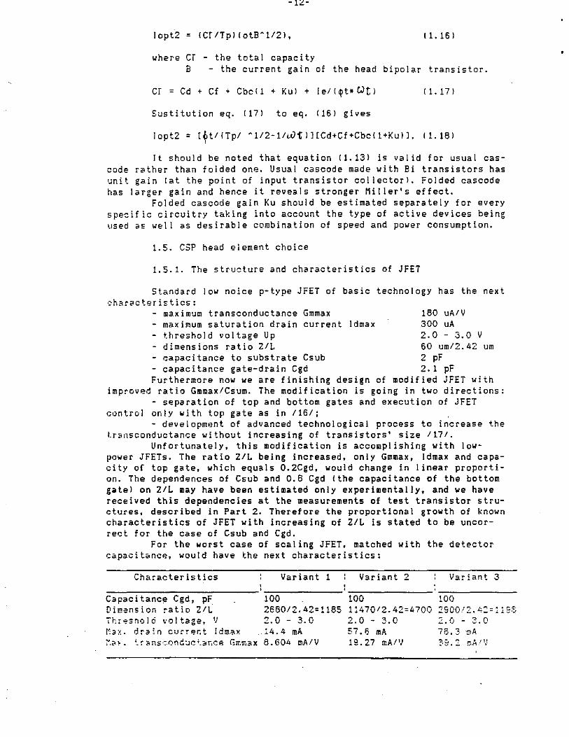
1.5. CSP head element choice
1.5.1. The structure and characteristics of JFET
Standard low noice p-type JFET of basic technology has the next char~cteristics:
- maximum transconductance Gmmax 180 uA/V - maximum saturation drain current ldmax 300 uA - threshold voltage Up 2.0 - 3.0 V - dimensions ratio ZIL 60 um/2.42 um - capacitance to substrate Csub 2 pF - capacitance gate-drain Cgd 2.1 pF Furthermore now we are finishing design of modified JFET with
improved ratio Gmmax/Csum. The modification is going in two directions: - separation of top and bottom gates and execution of JFET
control only with top gate as in 116/; - development of advanced technological process to increase the
t.r.3nsconductance without increasing of transistors' size 1171. Unfortunately, this modification is accomplishing with Jow
power JFETs. The ratio Z/L being increased, only Gmmax, ldmax and capacity of top gate, which equals O.ZCgd, would change in linear proportion. The dependences of Csub and O.B Cgd !the capacitance of the bottom gate> on 2/L may have been estimated only experimentally, and we have received this dependencies at the measurements of test transistor structures, described in Part z. Therefore the proportional growth of known characteristics of JFET with increasing of Z/L is stated to be uncorrect for the case of Csub and Cgd.
For the worst case of scaling JFET, matched with the detector capacitance, would have the next characteristics:
Characteristics
Capacitance Cgd, pF Dimansion ratio ZIL ihro:-snc.1l6 voltage, 11 M3x. drain curre~t Idmax ~?•. ~ranscond~ct~nce Gremax
Variant 1
100 266012.42=1185 2.0 - 3.0 14.4 mA 8. 604 mA/V
Variant 2
100 1147012.42=4700 2.0 - 3.0 57. 6 mA 19. 27 mA/ 11
Variant 3
100
2.0 - 3.0 76.3 mA

•
-13-
Table 1.2 summarizes JFET white noise calculation results !flicker nolce Is not taken into accountl and minimum power dissipated only by the head JFET:
Pmin = ld•Vp!ld/ldmaxl'l/2 ( 1. 19 J
Estimates to be shown are made for operational current Id which is equal that of ref. 1101, i.e. Id= 200 uA, and provides the desired level of noise.
Characteristics
ldmax, mA Gmmax, mA/V er = Cd + Cf + Gin, pF Id !operational valuel, mA
Gm !operational valuel, mA/V ENC4, r.m.s. e- !•I Pmin, mW
Variant 1
14.4 8.604 200,5
0.2 0.523 5500 0.071
7.33 4.0 2000 15.7
• Rounded to hundreds of electrons.
Variant 2
57.6 19.27 200,5
0.2 7.07 0.576 4.0 5300 2000 0.035 7.43
Table 1.2
Variant 3
78.3 39.2 200,5
0.2 2.94 1. 003 4.0 4000 2000 0.0303 1. 71
1.5.2. The structure an characteristics of bipolar transistor
Combined BJT-JFET technology provides the next low-power n-p-n transistor parameters:
B = 70, le = 3.0 mA, Fr >= 2.5 GHz, brea.kdown collector-emitter voltage Uce > 6.5 V lib= OJ, Ccb < 1.2 pf !Ucb = OVJ.
If Bi transistor were used in CSP input stage connected to detector with internal capacitance Cd= 100 pF, the dimension optimization would be reduced to Rbb' minimization only, ·and capacitance matching would be made by collector current changing. These estimates have been made for three variants of the head Bi transistor.
Characteristics
Overall emitter zone area, um Spread base resistivity Rbb', Ohm Collector-base capacitance Ccb, pF Transition frequency Fr, GHz Current gain B
Variant 1 : Variant 2
.300 x 2.5 6 2.4 2.5 70
150 x 2.5 12 1. 9 2.5 70
Variant 3
90 x 2.5 20 1. 7 2.5 70
Minimum possible power dissipated by the head transistor has been estimated too:
Pmin >= 0.8B•le ( 1. 201
The results are summarized in Table 1.3.

-14-
Table 1.3
Characteristics Variant 1 :variant 2:variant 3
loptl !capacit.matchingl, mA 42.98 42.58 42.41 lopt2 lmin.ENC1"2+ENC3"21, uA: 27.3 !B=1001
B : 70 22.9 22.7 22.6 B = 50 19.4
Rbb', Ohm 6 12 20 le !operational value>, uA 200 20 2.0 200 200 Gm I operational va I ue >, mAIV 7.69 0.769 0.0769: 7.69 7.69 Ci=2Cbc+ 1 el! al* fl;Ku=l, pF 5.29 4.85 4.805 ' 4.29 3.89 ' er =Cd+Cf +Ci. pF 105.8: 105.35: 105.305 104.6 104.4 Pm in, uW 160 16 1. 6 160 160 ENC!, r. m. s. e- {*) 660 2080 6560 650 650 ENC2, r. m. s. e- {*) 190 190 190 270 350 ENC3, r. m. s. e- ( *)' B=100 4810 1520 480 4810 4810
B=70 1820 B=50 2150
ENC sum, r.m.s. e- ! *I' B=100 2580 B=70 2770 B=50 3000
Ccb, pF 2.4 1. 9 1. 7
( * ) Rouned to tens of electrons.
1.5.3. Main conclusions about the head element choice
Analysis of' data shown in Table 2, 3 permits to make the next conclusions:
1.5.3.1. About usage of bipolar transistors for the case of Cd= 100 pF and Tp: 1 us:
- the series noise minimization achieved by optimization of the head transistor emitter current loptl leads to unacceptable increasing of the parallel noise ENC3;
- the emitter current optimization should be made by minimization of ENC1"2 + ENC3"2. In this case we get lopt2 = 15 - 30 uA for different head trasistor structures and B's;
- distinctions of the Bi transistor structures don't affect noticebly on the total noice level because contributions of ENC2 and ENCl versus Cbc are very small in comparison with those of ENC3 and ENCi determined by the input current and transconductance;
- to achieve more realistic estimates of ENC one should use more precision values of Ku and the experimentally measured dependence ENCi on Gilt= rut1Je) and lopt2 in the region of microcurrents !le= 1 .•• 100 uA>;
- use of the bipolar transistor in the input stage of CSP is not the best decision in the sense of noise because in the case of Cd = 100 pF, Tp = I usec, B = 50 ••• 100 and optimal emitter current about 20 uA resulted noise is equal 2500 - 3000 electrons without taking into consideration noises of detector leakage current and CSP feedback resistor;
- the main advantages of BJT transistor in the mentioned case are very small occupied area in comparison with JFET, rather small dissipated ·power and higher speed.
1.5.3.2. About use of JFET in the case of Cd = 100 pF and the peaking time Tp.• l.usec.it should be noted the next:

-15-
- all JFET variants provide the required noise level ENC= 2000 e- taking into account the noise 110 e- produced gate leakage current about 10'-9 A and different minimum values of the head element dissipated power 15.7 mW, 7.43 mW and 1.71 mW;
- variants 1 and 2 of JFET structures provide the same noise le~ vels but JFET of variant 2 being of the same design rool occupies 4 times greater area and dissipates two times less power;
The most suitable for use as the head element is JFET of vari-ant 3;
- electrical circuitry of CSP should give a possibility to vary the head transistor drain current because this permits to provide the best combination of noise !regulated by Gml and power dissipation !regulated by ldl.
1.5.3.3. These calculations have estimation nature. After taking into account characteristics of the new designed p-JFET's now we hope to attain more precise estimates in future.
1.6. Choice and calculation of readout path tCSP + slow shaper I
!.. 6. !. Prel lminary notes
L1~t us !':'Stim~te the noise contribution of factors being unk:--:cw at the beginning of this design, namely: the detector leakage curr~nt I'. an~ paral'.el rasiatan:e Rp (parallel connection of CSP feedback resister Rf ~•id -J~:.;ctor Liase resistor Rbi. If Rb is absent, i.e. Rb :<(;70, Rp = Ef, ar-.d w~ h~~·~
r.om 10 MOm 50 MOm 100 MOre
ENC5 770 e- 240 e- 110 e- SC• e-
! 1 10'-11 A 10'-10 A 10'-9 A 10'-7 A 10'-6 A ---------- -------
ENC3 10 e- 30 e- 110 e- 1080 e- 3420 e-
Eq. !6l includes components, being dependent on Tp, both increasing and dec:easing, so it possible to find the optimal peaking time
Tp opt= 2CTC!tt*Rpl/3Gm!2~t + Rptll + linll'l/2 1.6.2. Calcula ion of CSP and slow shaper
!1.21l
Readout path configuration is shown in fig. 1.1. Let us choose basic p-JFET with ZIL = 6012.42 as the head element of the slow shaper and JFET of variant 1 for CSP. Then we obtain the next characteristics:
Slow shaper:
Feedback capacitance Cfs Coupling capacitance Cc JFET dimensions
0.5 pF 4. 0 pF 60 um/2.42 um

-16-
JFET transconductance: maximum Gmmax operatinal Gm
Peaking time Tp Operational drain current Id Feedback resistor Rfc Total shaper capacitance Cts = Cc + Cis + Cfs Input shaper capacitance Cis lMiller's effect is neglected, i.e. Ku= Ol Output shaper capacitance Cos = Cfs + parasitic capacitance 0.1 pF Load capacitance lneglectedl Shaper's gain Avs
CSP:
Feedback capacitance Cf Feedback resistor Rf p-JFET dimensions Transconductance: maximum Gmmax
operational Operational drain current Id Total gain lCSP + slow shaperl Total noise !CSP+ slow shaperl:
head JFET feedback resistor Rf total
Drain current Id provided ENC = 3000 elGm = 1.761 mA/VJ Minimum power dissipated by the head JFET when ENC = 3000 e-
1.6.3. The timing channel calculation
180 uA/V 15.58 uA/V 1. 003 usec 8. 2 uA 3.9 MOm 6. 6 pF
2.1 pF
O. 6 pF 0 pF 15.55
O. 5 pF >SO MOm 286812.42 um 8.6 mA/V 4.0 mA/V 7. 33 mA 11.44 mV!fC
2000 e-110 e-
2010 e-
l. 98 mA
2. 2 mW
The main timing channel characteristics are the time jitter Ti and the time walk Tw:
where
where
Tw = Twl + Tw2 11. 221
Twl - the component stipulated by the shaper pulse rise time lwa.vefront steepness! dependance on a value of output voltage;
Tw2 - the component conditlned by comparator time delay due to input signal value.
Twl = 1Tps2•Ut/Avf•Avs2lll/Qinl + 1/Qin2l ( 1. 23)
Tps2 - fast shaper peaking time Ut comparator threshold Avf•Avs2 - overall trigger path gain <CSP+ fast shaper>. On another hand the circuit parameters are chosen to satisfy
the next inequality:
( 1. 241
where Qint - input current causing the comparator switch on;

-17-
Taking into account eq. 11.211, we have
Twl <= Tps21Qint/Qin1 - Qint/Qin21 I 1. 25 I
For threshold value given in specification /9/ Qint/Qinl = 0.5, Qint!Qin2 = 1 we have Twl <= 0.4 Tps2, and since Tw < 4 ns the next uneqation is val id
Tps2 < 10 nsec.
From eq. 11.241 for known Qint = 16 fC, Ut = 5 uV and Avf = 0.735 we get
Avs2 > O. 431.
The time scattering dispersion is known to satisfy the equation
Ot·z = u'2/Cdultl/dtl'2. ( 1. 26 I
In our case this equation transforms to
G't = Tps2140 fC,..ENC = 10 nsec•0.48 fC/40 fC = 0.12 nsec.11.271
The jitter is supposed to be measured with the input charge 40 fC provided that signal amplitude dispersion is considered to becaused only by the input noise transfered through the whole system CSP +
fast chaper. Summarizing this discussion we have to state the next requirements tc the fast shapers:
Parameter
Tps2 Avs2
Required
< 10 nsec >0.431
Desired
<10 nsec >0.86
1.6.3.1. The fast shaper head element choise
The fast shaper head element type choise was based on the peaking time calculation method of ref. 1101. It should be noted that this method is fully correct for OTA with voltage controlled head element IMOSFET or JFET) only. For Bi transistors its results may be co\idered to be rather qualitative than quantitative.
Accoring ref. JlO/ the peaking time is estimated to be equal
Tps2 = 2Cts2/tGms2•Cfs2/Cos2 + l/Rfs21 ( 1. 281
The next types of electronic devices were considered for use as the head element of the fast shaper: low-power p-JFET, low-power JFET's of variants 1,2 and 3, Bi transistor and MOSFET with characteristics recovered from ref. /10, 131, namely for low-power MOSFET:
Z/L = 39010.8, Gm = 220 uA/V provided that Id = 10 uA, Ci= 0.5 - 0.7 pF <Miller's effect has been taken into account I,

-18-.
and for high-power MOSFET:
ZIL = 400010.8, Gm = 3 mA/V provided that Id = 200 uA, Ci = 6 . 9 - 7 . 1 pF.
High-power JFETs of variants 1, 2 and 3 used in calculations had the characteristics shown in Table 1.1, but in addition we have made an attempt to get a real scaling of capacitance Cgd taking into consideration 20% contribution of the top gate made in the total capacitance value.
JFET's variant:Gmmax, mAIV:Cgd, pF, the worst case:Cgd,pF, the real case
1 2 3
8.604 19.27 31. 6
100 100 100
24.7 84.7 24.7
The calculation results obtained for Cfs2 = 10 pF, Cc2 = 0.5 pF are shown in table 1.4.
Active device used
MCSFET Low-power
Table 1.4
: Input ca pa-: Transconductance, mA/V : c i ta nee, : pF
:------------------------------------ma:-:imum : for Tp=lO.O nsec
0.6 0. :: fc·r Id= 10 uA: :. 73 mA!\1
----------------~-----------:-------------------:----------------
jFET
case,
ld=7S.~ m/..
More realistic sealing,
7.0 3.0 for ld=200 uA: 4.35 mA/V
var.1: 100 8.64 27. 18 -----:-----------:-------------------:----------------var.2: 100 19.27 27.18 -----:-----------:-------------------:----------------
100 31.6 27.8
var.1: 24.7 8.604 8.66
-----:-----------:-------------------~----------------var.2: 84.7 19.27 23.4 -----:-----------:-------------------:----------------
ld=17.S mA var.3: 24.7 31.6 8.66
JFET, I ow-power 2.1
Bipolar transistor 1. 2
Cfs2 = 10 pF, Cc2 = 0.5 pF
0.18 3. 1
2. 88 for Id = 74.9 uA
Data of Table 1.4 permits to state that the fast shaper with the peaking time of about 10 nsec can't be relised using the CMOS technology with parameters, specified in ref. 110, 13/, because the transconductance far this purposes should to be 1.45 times greater.

-19-
Among the proposed JFETs only var.3 permits to make 10 nsec shaper, but it demands Id = 75.3 mA in the worst case. Both this value and the more realistic Id= 17.5 mA are unacceptable due to the high power dissipation.
Such a shaper seems to be realised only with low-power Bi transistor at relatively low operational current 75 uA, but it should be noticed once again that the calculation method being applied to Bi transistors gives large errors in the case of their operation with emitter currents greater than 0.5 uA, so these results appear to be rather qualitative in nature.
To the fire end let us provide the parameters calculated for the fast shaper used Bi transistor as the head element. Since the fast shap~r introduces additional noise, the parameters has calculated for two cases: for optimum emitter current !opt and the least noise !without taking into account the feeback resistor noise! and for the similar case but with enlarged Rfs2.
Table 1.5 The fast shaper specification
CCfs2 = 0.5 pF, Cc2 = 0.5 pF, Cos = 3.0 pF, Cts = 2. 1 pFl
lopt2 88 uA le operational 90 uA 56.2 uA Gms2 3.46 mAtV 2. 16 mAtV Tps2 7.15 nsec 10.9 nsec Rfs2 100 kOhm 40.9 kOhm Avs2 6.99 1.876 Avf•Avs2 5.146 mVtfC 1.38 mV!fC ENC5, r. m. s. e- (<) 250 390 ENC3, r. m. s. e- I• l 450 360 EN Cl, r.m.s. e- I• l 110 140 ENC2, r.m.s. e- I• l 70 70 ENC sum, r. m. s. e- { *) : 530 550 du/dt 28.79 nV/nsec: 5.52 mVtnsec
Jitter due to the shaper noise: 0.006 nsec 0.032 nsec Total jitter 0. 120 nsec 0.124
Jn the final variant the fast shaper parameters should be recalculated taking into consideration the real values of Ku and components' parameters.
1.7. The CSP head-element estimation for the peacking time 1.0 and 0.3 usec and noise levels 3000 and 1000 r.m.s. e-
During accomplishing of this analysis we received a .suggestion ta investigate the possibility ta achieve noise levels 3000 and 1000 r. m.s. e- at peaking times 1.0 and 0.3 us.
The head element estimation was made by the same method used for the calculations of JFET structures of the variants 1, 2, 3 and the bipolar transistor structures of the variants 1, 3 lsee parts 1.4., 1.5. >. The calculation results are summarized in Table 1.6.

-20-
JFET Variant 1 Variant 2 Variant 3
Id max, mA 14.4 57.6 78.3
Gm max, mA/V 8.604 19.27 39.2
CT. pF 200.5 200.5 200.5
Tp, usec 1. 0 0.3 1.0 0.3 1.0 0.3
IENC3'2+ENC5'21'112, r.m.s~e- 153.7 84.2 : 153.7 84.2 : 153.7 84.2
ENCsum:ENC4,r.m.s.e- 2996 2999 : 2996 2999 : 2996 2999 :-----------------------------------------------------------
3000e-:Gm, mAIV 1.784 5.935 : 1.784 5.935 : 1.784 5.935 :-----------------------------------------------------------
r.m.s.:Id operat, mA 1.989 11.76: 1.796 15.64 : 0.620 6.134 :-----------------------------------------------------------: Pm in, mlJ 1.848 26.57 : 0.793 20.37 : 0.138 4.292
ENCsum:ENC4,r.m.s.e- 988 996 : 988 996 : 988 996 :-----------------------------------------------------------
1000e-:Gm, mAIV 16.4 53.21 : 16.4 53.21 : 16.4 53.21 :-----~-----------------------------------------------------
r.m.s.: Id operat, mA NO NO 55.07 NO : 34.28 NO :-----------------------------------------------------------:Pmin, mW NO NO : 134. 66 NO : 56.07 NO :-----------------------------------------------------------
================================================================== n-p-n Variant 1 Variant 3 Comments ------------------------------------------------------------------Rbb', Ohm 6 20
Tp, usec 1.0 0.3 1.0 0.3
lopt2, 8=70, uA 22.9 76.3 : 22.7 75.7 ---------------------------------------------------ENC2, r.m.s. e- 190 347 : 348 634
ENC3, r. m. s. e- 1943 1952 : 1934 1936 8•70, le•lopt2
Gm, mAIV 0.881 2.93 : 0.873 2.91 le•lopt2 ---------------------------------------------------EN Cl, r. m. s. e- 1940 1942 : 1946 1946 ---------------------------------------------------ENCsum, r.m.s. e- 2746 2769 : 2767 2816 ---------------------------------------------------Pmin, ull 18. 32 61. 04 : 18. 16 60.56 ---------------------------------------------------lg = 10'-9 A, Rf = 50 kOhm NO - the .implemenat!on is .impossibl.e.
Being analyzed they permit us to make the next conclusions: -.BJT of all the constructior,fconsidered don't allow to at
tain a noise ·level· lower than 2700 e-;

-21-
- decreasing of the peaking time to 0.3 usec leads to 3.3 times incresing of the power dissipated by the head transistor with the same noise level supported;
- al 1 the considered constructions of JFETs don't allow to provide ENC = 1000 e- at Tp = 0.3 usec;
- it were possible to attain ENC = 1000 at Tp = 1.0 usec with JFETs if the power dissipated by the head transistor would increase to 135 mW and 56 mW for JFETs of variants 2 and 3 respectively.
Jn addition it should be noted that detector leakage currents were not taken into account in this estimation, and the active elements were considered to work in the theoretical limiting case of the saturation region boundary where the dissipated power is minimum. Jn the real circuits the transistors will be far of the saturation due to impossibility to stand the operational regime precisely, so the real head-element power dissipation will be greater than the theoretical one. Moreover, some additinal power will be dissipated by another elements of the circuit especially by the fast shaper with the peaking time RC-CR of 10 nsec.
1.8. The CSP CMOS JC production possibi 1 ity estimation for the case ENC=1000 r.m.s. e- and Tp=300 nsec
1. 8. 1. General notes
The estimation was made for a CMOS charge-sensitive preamplifier ICSPI with a RC-CR shaper according to the methodics used above for BJTs and MOSFETs with addition of the eq. 11.29 -1.311 taken froci ref. l10J. A MOSFET flicker noise component is supposed to be equal
ENC6 = !Ct•elql•(Fk/l2W•Leffll'l/2. ( 1. 29 I
A bulk-resistance and a channel noise components are equal
ENC? = ICt•elql•(Rb•Sl'2•kT1!2Tpll'l/2 11. 30)
and
ENC8 = ICt•elql•[~ISl+llkTl!3Gm•Tpl, 11.31l
respective I y,
where: a the excess noise factor, SJ=Cdep/Cox - the slope factor, Rb - the bulk resistance, the rest of terms are the same as in part 1.3. above.
1.8.2. The comparison of existant CMOS CSPs
Different implementations of CMOS CSPs known from literature (8, 10, 13, 20l were analysed with reference to GEM muon detector appl ic;tion. This work happened to be rather difficult due to absence of the exhaustive information needed for the noise level recalculation for the detector capacitance Cd=100 pF and the peaking time 300 nsec.
Furthermore, there are different approachs to noise estimation and results presentation accepted in the publications, namely:
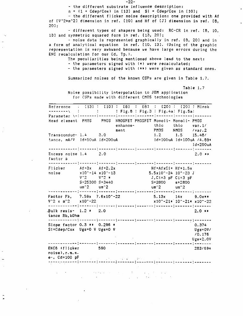
-22-- the different substrate influence description: n = !l + Cdep!Coxl in [131 and SI= Cdep/Cox in [101; - the different flicker noise description: one provided with Af
of [V"2•m"2l dimension in ref. [10] and Hf of [Jl dimension in ref. [8, 201;
- different types of shapers being used: RC-CR in ref. [8, 10, 131 and symmetric squared form in ref. [ 13, 20l;
- noise data is represented graphically in ref. [8, 20J and in a form of analytical equation in ref. [10, 13J. !Using of the graphic representation is very awkward because we have large errors during the ENC recalculation for our Cd, Tp. I.
The peculiarities being mentioned above lead to the next: - the parameters signed with !•l were recalculated; - the parameters signed with !••I were given as standard ones.
Summarized noises of the known CSPs are given in Table 1.7.
Tablel.7 Noise possibility interpolation to JEM application
for CSPs made with different CMOS technologies
Reference --------\
cl3J : [lOJ : [8J Fig.8
[8]
Fig.3 [20J : [20J : Minsk
Fig.4a: Fig.Sa: Parameter \-:-------:-------:-------:-------:-------:-------:-------Head element PMOS ?MOS NMOSFET PMOSFET Monoli- Mono! i- PMOS
enhance- thic thic var. l/ ment PMOS NMOS /var.2
Transconduc- 1. 4 3.0 1. 2 1. 5 15.48/ tanca, mA/V Id=SOuA ld=200uA Id=lOOuA ld=lOOuA 14.89•
ld=200uA ------------:-------:-------:-------:-------:-------:-------:-------Excess noise 1.4 factor a
2.0 2.0 **
------------:-------:~------:-------:-------:-------:-------~-------F 1 icker Af =3x Af=2.2x Hf=AfxCi= Hf=1.5x noise x10"-14 xl0"-13 5.5xl0"-24 10·-23 J
v·2 V"'2 • J,Ci=3 pF Ci=3 pF 5=25300 5=3440 5=2800 s=2800 um"2 um·2 um'2 um"2
------------:-------:-------:-------:-------:-------:-------:-------Factor Fk, VA2 lC m"·2
7.59x 7.6xl0"-22 x10·-22
5.13x 14x 9.0x .. xl0"-21• 10"-21• xl0"-22
------------:-------:-------:-------:-------:-------:-------:-------Jlulk resis- 1.2 • '
2.0 2.0 •• tance Rb,kOhm ------------:-------:-------:-------:-------:-------:------7:-------Slope factor 0.3 •• 0.296 • Sl=Cdep/Cox Ugs=O V Ugs=O V
o. 374 Ugs=OV/ /0.176
Ugs=2.0V ------------:-------:-------:-------:-------:-------:-------:-------ENC6 If! icker noise), r.m.s. e-, Cd=lOO pF
590 283/694
-~---.-------:-------:-------!-------:-------:-------:-------:-------

-23-
------------:-------:-------:-------:-------:-------:-------:-------1 2 3 4 5 6 7 8
------------:-------:-------:-------:-------:-------:-------:-------ENC? lbulk resistance noise l, r. m. s. e-,Cd=lOO pF, Tp=300 nsec
989 Ugs=2.0V
1488/ I 1153
------------~-------:-------:-------:-------:-------:-------:-------Reported 400+33Ci noise level, r.m.s.e- Tp=350ns
160+12Ci 5067 1500 2500 Cd=lOOpF Cd=lOOpF Cd=30pF
Tp=1.5us Tp=500nsTp=1.0us Tp=lOOns
2290 Cd=30pF Tp=lOOns
------------:-------:-------:-------:-------:-------:-------:-------Interpolated 3930• noise ENCsum for Cd=lOOpF, Tp=0.3 ns, r.m.s.e-
2752•
• The interpolated value •• The standard value
6542• 2739• 4811• 4407• 2435/ 2951
1.8.3. The CSP parameters to be aqchieved with CMOS technology available in Minsk
CMOS technology used in Minsk is intended for production of digital and simple analog-digital LSI/VLSI, so the noise parameters of MO~FETs were not investigated. To estimate ENC of CSP the standard valYes of I, Fk and Rb have been chosen lsee Table 1.71.Two construe-lions of a head p-MOS tr3nsistor were estimated: with capacitance mat::hi::.g 3nd will:out it.
~h~ !nput c~p~ci~jnce matching wl 1.'•; ~ dBtio;-ct:J: C:i=fCd•Cfl/3 Tlie j~,h~nsion ratio W/L The transconductance Gm at !d=0.2mA The noise 1ev.::is, r.rr.s. e-:
ENC6 ENC? ENC8 ENC5 ENC sum
1.8.4. Short conclusions
Variant 1 yes, Ci=33.5 pF 32300um/0.9um 15.46 mA/V
283 1488 1903 109.3 2435
Va: iant 2 :10' Ci=3.35 pF 3230um/0.9um 4. 69 mAIV
694 1153 2624 109.3 2951
The results of the investigations given in Table 1.7 allow us to make the next conclusions:
- no one of CSP reported in literature can provide the noise less than 2700 e- with Cd=100 pF and Tp=300 nsec;
- the least achievable noise about 2400 e- could be expected with MOS transistor of variant 1 which can be made with CMOS technology available in Minck too;
- the gigantic size of such a transistor <32.3 mml is supposed to lead to a low yeld and, consequently, to high prise of !Cs.
[
-24-
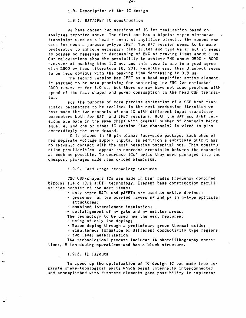
1.9. Description of the IC design
1.9.1. BJT/JFET IC construction
We have chosen two versions of IC for realisation based on analyses reported above. The first one has a bipolar n-p-n microwawe transistor used a~ a head element of amplifier circuit, the second one uses for such a purpose p-type JFET. The BJT version seems to be more preferable to achieve necessary time jitter and time walk, but it seems to posses no reserves in decreasing of ENC at peaking times about 1 us. Our calculations show the possibility to achieve ENC about 2500 - 3000 r.m.s.e- at peaking time 1.0 us, and this results are in a good agree with 2800 e- from I iterature [8, 20]. Nevertheless, this drawback seems to be less obvious with the peaking time decreasing to 0.3 us.
The second version has JFET as a head amplifier active element. It assumed to be more promising for achieving low ENC !we estimated 2000 r.m.s. e- for 1.0 us, but there we may have met some problems with speed of the fast shaper and power consumption in the head CSP transistor.
For the purpose of more precise estimation of a CSP head transistor parameters to be realised in the next production iteration we have made the two channels of one IC with different input transistor parameters both for BJT and JFET versions. Both the BJT and JFET versions are made in the same chips with overall number of channels being equal 4, and one or other IC version !two channelsl is wired to pins acccordingly the user demand.
IC is placed in 48 pin planar four-side package. Each channel has separate voltage supply inputs. In addition a substrate output has no galvanic contact with the most negative potential bus. This construction peculiarities appear to decrease crosstalks between the channels as much as possible. To decrease !Cs' prise they were packaged into the cheapest packages made from oxided aluminium.
1.9.2. Head stage technology features
CSC CSP/shapers !Cs are made in high radio frequency combined bipolar-field !BJT-JFETJ technology. Element base construction peculiarities consist of the next items:
- only n-p-n BJTs and pJFETs are used as active devices; - presence of two burried layers n+ and p+ in n-type epitaxial
structures; - combined interelement insulation; - selfalignment of n+ gate and n+ emitter areas. The technology to be used has the next features: - using of only ion doping; - Boron doping through a preliminary grown thermal oxide;
simultaneus formation of different conductivity type regions; - two-level metallization. The technological process includes 14 photolithography opera
tions, 8 ion doping operations and has a block structure.
1.9.3. IC layouts
To speed up the optimization of IC design IC was made from separate cheme-topological parts which being internally interconnected and accomplished with discrete elements gave possibility to implement

-25-
the desired functions. This parts were different both in chematics and in head transistor construction. The BJT version contains:
- similar in the two channels slow (signal I and fast I trigger I shapers having a head n-p-n made with a design rule h = 1.5 um, a number of emitter strips n = 3 and Rbb'= 93 Ohm, AREA= 0.3;
- different in the two channels CSP head transistors: channel 1 !input pin 451 - h = 1.5 um, n = 3, Rbb' = 93 Ohm, AREA=0.3; channel 2 I input pin 051 - h = 1.5 um, n = 10, Rbb' = 15 Ohm, AREA = 1.0; this transistor was supposed to be basic one for model constructions and measurements;
- a scaling factor for minimum size n-p-n AREA= 0.012; - all the JFETs are the same and have.Uth = 2.6 V; VT4, VT5,
VT7, VT13, T16 have AREA= 0.117, VT10, VT11 have AREA= 0.091. The TA2 connected-gates JFETS measurements results listed in part 2.6 correspond to AREA = 1.5;
- a protective died chain is placed only in channel 1 and operates with a biased substrate and zero potential on the channel 1 ground pin 10 Vat pin 47 and -Ecc at pin 241.
The JFET version containes: - similar in the two channels slow and fast shapers having
h~ad pJFETs with AREA = 0.235; - output pJFETs with AREA = 0.235; - channel 1 and 2 differ by the head element:
channel 1 !input pin 21 has pJFET with AREA= 1.5; channel 2 !input pin 51 has pJFET with AREA= 1.0;
- al I the n-p-n transistors have the same sealing factor AREA = O.Oi2;
- al I the resistors of al I the channels have 60~ overstated values in reality compared with nominals to be supposed.
The large number of the interconnections lead to a large number of contact pads whose size and pitch determine the die size. The contact pads are placed on two rings 144 pads for BJT version 1 and 34 pads for JFET version 2>. Inside area of the internal contact pad ring is occupied by two JFET version channels and two BJT version channels together with test array TA2 dedicated to optimize the technological process and constructions of the head transistors.
The overall single channel size without contact pads and RC-CR elements equals:
1300 x 300 um for version 1 rBJT l - 1100 x 400 um for version 2 !JFETl.
1.9.4. Electric circuits of BJT version
As it was mentioned above one readout BJT-version channel contains CSP, fast shaper, slow shaper supplied by two separate equal biasing networks. The BJT version channel 1 electric circuit is shown in Fig. 1.2, the channel 2 circuit, being identical except of pin designation, is shown in Fig.1.3. CSP consists of transistors VT2, VTS, VT6, VT10, VT11 and VTc2. VT2 is the low noise input !headl transistor !different in channels 1 and 2> having rather large size to minimize thermal series noise. VT5 is a p-channel JFET. VT5 cascades the VT2 and is loaded with current generator VT6. Application of the active load !current generator VT6l allows to increase the gain and gives the pa~•ibllity of adjusting of the standing current. VT10, VT11 form an output buffer, where the capacitance feedback is closed. Jt is implement~d with JFETs rather than with BJTs because such a configuration is more suitable when the output signal Is negative.

Channe 1 1 Afl>I 23 -...,
s ~:J 24
,,, "" ""' "'i'
... , 27 44 41 34 33
' .. " "" 22~8 ~~ .... ,
Cinl
.
25 j ~·
28
29 4~
46 . ,_.,__
~ C<.nJ 37
F .. t -.._-
• • lO ""' 9
IP ftll II Z.:ol;
19 ""' ~ ,__.,..., JS : o:
---• •
<>------1'1---~··~''->--r---'-t~·~~---'.i:.~ t1 I 36 . "
48 2 •
'~--->1 24
• "J : ~":'
29'" 39 I<:';.
...
~" " a~11
26
llc...e<ll 19 Re: ... ~:
40 ....
,...,z " .... , 39 ""
~· " ""' 38
.. .t3 21 lk_eottl .
35 -
...., 32
Fig.1.2. The bipolar version of IC

( ( I {
Ml 23 -M"
5 L:J 2t
Cl~
"' ,,, "'' ..... I
21 6 8 15 16
• "" " "" 22 ~2t ~~
23 - , ... ·~-• • I 20 "
W< 9
I '" 3 '"' 3 "~ •• "~ " ' - • ~ r ~ 3J UpF .. ;,. .2.1t
19 .... ~ ci.--n1.,. v.....ilf1..- 1.>1 .. ""'..--
I.
: ~'~ •m• •• ., ~ - 5 ~. • 8
" "'~ ' "" ' "" ' " " ~ii
I ~" t--1 r, tlJ \!: 3 - •• • M
6 • ·~ "'19.._ • . • .. 23 OA'l4 37 .... ~
' " r: -~ ... ~ 4 ~
' " ~ " ~(1t1t " " ~ ~ ~ 1. w •• ..•
m~-•1_..,. _ _...
• .. ~ .. • K UK
" ..!!J. !!!. 42
" .. 12 w " 31 ti: ..
I ~· , ... , " - ,,,,. .... r.
~ t-I 13 ~ " c.., ... ,. •• • " • - " r: " ~· -·-2 .. ,,
''1~ ... .. :: I ~ "' o~
.. - a c• ' •.
I 12~
' - "
. .--.._!
L
~ ..
~'
.. - ""''12
-"• .,, - ..
" ~ -• • •
k•t3
-- ..... -.. , ... ·- -" --•• •
22 "
3 "
JO «
J J "
14
"
17 " 18 "
J
O•H
Jk-e-•~ -... t.? ... ~·2
~c ... e"3 -..... ·-~"
J
' ~ ~
'
)

-28-
The high speed in this amplifier is obtained, since VTl has very high transition frequency at low standing current and VT2 has very small dimensions with, consequently, a neglegible output parasitic capac i ta nee.
The biasing networks are separate and identical for the CSP and for the slow shaper.
The standing currents of transistors VT2 and VT5 are setted through the current mirror VT6-VTc2 by the resistor Rc_ext2, external to the chip.
The CSP biasing network !VT13 - VT15, VT19, VT21, VT23, VT25, VT27, VT29l also provides insensitivity of CSP to changes of a threshold voltage of JFET VTS. No matter, what concrete value of the threshold voltage VTS has !in reasonable limits, of course!, the biasing network wil I set such potential on the gate of VT2, that it wil I be in the nominal current mode. It consists of a multistage current mirror VT16, VT21, VT27 and VT29 with external setting of working currents with the external resistor Rext2. The difference stage VT19-VT21 compares voltage dictated by the drain current of the reference JFET VT13 being identical to the cascode JFET VTS of CSP, with the reference voltage made by the stable current of VT27. As VTS and VT13 have similar size and construction they have similar both threshold voltages and their drifts, which are compensated by the biasing circuit.
In order to get the best compromise between speed, noise and power dissipation the biasing of the preamplifier can be modified by means of external resistors. It should be pointed the need of separate sets made with Rext2 for the gate voltage of the cascode VTS and for its drain current made with Rc_ext2.
The circuit of the slow shaper <VT3, VT7, VTB, VT12 and VTc3l is somewhat alike that of CSP. The difference in the output buffer !the BJT rather that JFETl is caused by different polarity of the output signal. The standing currents of the slow shaper transistors are less than those in the preamplifier because there is no necessity of very fast operation here. This allows to diminish the total power consumption. Biasing of the slow shaper is identical to that for CSP and is made with external resistors Rc_ext3 and Rext3 trough the separate biasing circuit !VT16 - VT18, VT20, VT22, VT24, VT26, VT28 and VT30l being identical to the CSP biasing circuit and trough the same current mirror VT8-VTc3. It should be noted that in the next production iteration this external resistors RC_ext3 and Rext3 should be placed into the chip.
The fast shaper is somewhat simplified version of the same folded cascade circuit. The dimensions of the input transistor VTl here are mach less than that of the preamplifier, because the noises considerati.ons here are of no interest. So this transistor operates faster. The absence of the current generator in the drain circuit of the JFET VT4 also makes the circuit faster. This absence also decrease the gain, but it is of no importance here. The shaping time of the fast shaper, calculated with the emulating program SPICE, is about 25 nsec. The total power consumption in the nominal mode <Rext=lOOkl is estimated to be equal 60 mW (it is the calculated value!.
All the inputs and outputs of the six BJT amplifying structures of the !CSP + slow shaper + fast shaperlx2 are separated and led to chip pins as far as inputs and outputs of the two biasing circuits and the dinamic load transistors current setting inputs of CSPs and slow shapers. Such an o~ganlzatlon permits us to optimize the head transistor currents in all amplifying structures of the chip for minimizing noise levels and dissipated power, to connect feedback capacitors and resistors of different values to set different peaking time, to inves-

-29-
tigate the dependence of crosstalks on biasing circuit shared between the amplifier structures of a single channel and between the two channel of a single chip.
In addition all the head transistor emitters points are led to output pins to permit measurements of the head transistors currents and_ to investigate experimentally the possibilities of the electrical circuits structures optimization.
In the next design iteration we suppose to hide all the auxiliary inputs and outputs inside the chip, providing more large number of channels per package.
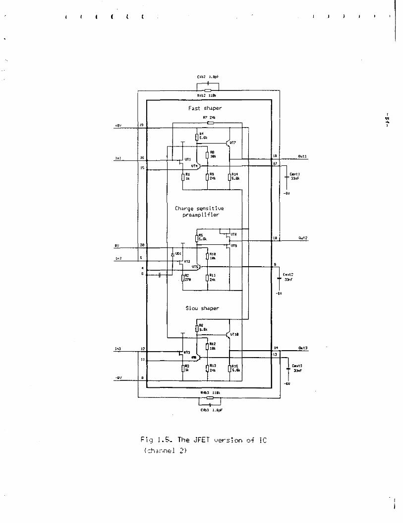
1.9.5. Electric circuits of JFET version
The second version with a head JFET seems to be more promising for achieving low ENC !we estimated 2000 r.m.s. e- for 1 usecl, but there are some problems with the speed of the fast shaper and power consumption of the head CSP JFET.
The JFET version IC is shown in Fig. 1.4 !channel 11 and in Fig.1.5 !channel 21. Their electric circuits are similar except of the size of the head CSP JFETs being mentioned above. The first CSP stage is a folded cascade, but the head transistor in contradistinction to the BJT version is p-type JFET, the cascade transistor is n-p-n. There is a JFET source follower at the output of CSP to make negative pulse front more fast. The fast and slow shape~s have n-p-n BJT emitter followers at their outputs beinng adopted for such a purpose with positive pulses. The bias of the cascade n-p-n is made with a resistor divider and a filtering capacitor, but in the second design iteration pull-down resistors are supposed to be replaced by diode chains. The CSP input is protected against large positive pulse voltages with a diode chain being connected or disconnected by wireing. The input-output ideology is the same as in the former case.
1.9.6. Pspise BJT version simulations
The proposed electric circuit of readout channel for the cathode strip chamber was simulated with Spice. The main goal of simulation was to get convinced in the operatability of the basic design concepts and to set more presiously the nominal values of passive elements and operating modes of transistors. Spice models of JFET and bipolar transistor were composed from measurement results of test specimens, which were produced earlier by the same technology. Full Spice model of the circuit and the simulation results including circuit response on the maximum input charge l200fCl are presented in fig. 1.6 - 1.8, and the Spice description of the circuit is presented in Appendix 1.
The simulation performed allows to predict some main parameters of designed integrated circuit. Voltage gain of charge sensitive preamplifier and slow shaper will be about 400, and voltage gain of fast shaper will be almost ten times less then that value. It is caused by the absence of active load in the fast shaper's cascade. Having less gain, fast shaper has much faster response. In the case of delta-pulse stimulation the risetime of output signals will be:
- for the fast shaper - about 40ns; - for the slow shaper - about 300ns; - for the charge sensitive preamplifier - about 40ns.

f (
•GO
'"'
'" '"'
,.,
-6'
C~b2 1.8pF ..
I R+b2 ""
Fast shaper
R7 24k
" "' JVT7 6.6k
" ~
"' 33 "" VTJ
' VT4"'
" " R9 "' .. "'" '·"'
Charg<:? sensit:t•.Je pr-eampl~.fier
R5 1-i;IJTa 6.6k
" T ' l- 'J1'i
' UDJ I "' ' ••• ~ UT2 •JTS._
' ' '
" "' Rll
"" '"
Slou shaper
.. JVT'8 '·"'
"" " ... ~ VT3
" '"" ., Rl3 "' " "'' 6.61:
" .. ., ,, .. I I Cfb3 J.lpl'"
F'. J 1.4. The JFET '1e1-£i•)r. of IC
:.:t:)nn~i 1}
)
31 011.tl
" 1 Cextl T J3nf.
""
19 Out2
" 1 ""' 31,..
_.,
,. ""' "
Ciro.t3 . """
..,,
' ... 0
'
)
(
+6•J
'"'
ll'J
'"'
'"'
·&V
Ctb2 J.BpF
I l:Ut2 110~
Fast shaper
R? 21k
J9
" J,,, S.6k . FIS
J6 , ..
"'' I u11:; "
Al " "" lk , .. '·"'
Cha~ge sensitive preamplifier
" ~IJTB '·"' 20 T ' ,,..
,.,.001 "' 5 , .. "' ' VTS" •
6 " Rll " "' 27' '"
Slow shaper
.. s.&k . VUI .
Al2
" , ..
' "" II .. ~
RJ "" "' lk , .. '·" • Afb3 Jiik
I I . C.fb3 l.&pF"
Fi 9 J. 5. The JFE T "er-s; on o-f IC (·:ha-:-1nf2l 2>
" Outl
" , 6 cextl
33nF
_.,
" 01.1t2
• .~ (ext::
'''" . .,
14 011.tl
13
.... c..t3 33nF
_.,
I
"' ... '

1.85
1.84
> 1.83
Q)
CT> 0 1.82
+-'
0 > 1.81
" ......... ::J o_
+-' 1 .80 ::J 0
1.79
1.78
-32-
Fig.1.6 CSA response (sirnulation)
I -----------------------,-----
-----r-----r-----r----1 I
-----~-----~-----! I
__ L _____ L _____ L _____ L ____ _ I I I I
I I I I I ---r-----r-----r-----r-----
-----r-----r-----r-----r-----1 I I I I I I I I
OE+OOO 2E-007 4E-007 6E-007 8E-007
time, s 1E-006

-33-
Fig. 1.7. Slow shaper response (simulation)
400 -----------------------------· .
2.00
> a) 0.00
CTl 0
+-'
0 -2.00
> +-'
:::::l 0... -4.00
+-' :::J 0
-6.00
I I I I
-----L -----L-----L _____ f
I
-L-----L----- -----L-----1 I I
I I
I I I I
---L-----L-----L-----~ I I I
I
----L-----L-----L-----L-----1 I I I I I I I I I I I I I
-----L-----L-----L-----L-----' I I I I I
-8.00-1-T'T'T".,....,...,,.....,.'T'i-,....,....,"'T"T"....,-,r-r+'T'T".,....,...,,.....,.'T"T"i--.-.,...,.......,...,....~+,-~~~~
DE+OOO 2E-007 4E-007 6E-007 BE-007 1E-006 time, s

-34-
Fig.1.8. Fast shaper response (simulation)
-4.20
-4.40
> a)-4.60
CTl 0
+-' 0 -4.80 >
+-' ~ o_-5.00
+-' ~ 0
-5.20
I I I I I ____ L _____ L _____ L _____ L _____ I
I I
I I I I ___ L _____ L _____ L _____ L _____ I
---L-----L _____ L _____ L ____ _ I I I I
-------~
I I __ L _____ L _____ L _____ L ____ _
I I I
I I I I I _____ L _____ L _____ L _____ L ____ _
I I I I I I I I
I I I I
-5.40 -1-r-rr-T"T"'T...,...,...,.+,....,...,. ....... .,..,...,....,+.....-,.......,...,...,..T"rlr..-r ......... ,....,..,..,....,.+..-....,...,.~.,..,..-ri OE+OOO 2E-007 4E-007 6E-007 BE-007
time, s 1E-006

-35-
The standing current of charge sensitive preamplifier input device can be adjusted in the range 0.5mA ••. 2.0mA by means of external current setting circuits.
The large number of external current setting circuits in the scheme of first iteration provides an ability to set circuit in the optimal operating mode even if real parameters of integrated elements would differ <in reasonable range! from ones used in Spice simulation.
The test electronic device measurements reported in the next Part 2. of this report were used to modify BJT and JFET Pspice models and face values of resistors. Figs.1.9 - 1.11 show the results of the refined Pspice stimulation, the Pspice circuit description is presented in Appendix 1 too.
1.9.7. Discrete elements BJT version breadboard modelling
The bipolar version of CSP made with discrete components on a breadboard was tested. The electric circuit to be modelled is shown in Fig.1. 12. The channel consists of CSP, SS and FS and has a common biasing circuit to compensate cascode JFET threshold voltage shift and to set collector current of the head CSP ransistor. The head CSP element VT! was made of four parallel connected low noise microwave transistors KT640A, the head transistors of SS and FS VT7 and VT11 as far as the CSP cascade load VT3 and the FSISS output emitter followers VT13 and VT10 are KT399A, field-effect transistors are the JFET double-transistor groups K504HT1A. All the res transistors forming the biasing circuit are five-transistor groups K19BHT1A. The model tests has shown the operability of all the parts of the circuit. The front edge was found to be equal 40 nsec for the CSP and 20 nsec for the fast shaper.
1.9.B. Pspise JFET version simulations
The electric circuit of the two channels of the JFET version IC is shown in Fig. 1.4, 1.5 and is described in part 1.9.5.
The JFET version CSP noise characteristic is determined in the the first order by head JFET VT2 transconductance G and gate capacitance Cg. At the first step of JFET version Pspice simulations G amd Cd were supposed to be equal 10 m/V and 5 pF respectively. Such a value of the transconductance gives a value Rs = 67 Ohm for series noise resistance of the JFET channel. The second simulation step was made after the mentioned above Pspice parameter modification. The head JFET of the channel 2 is considered to have Gmax = 15 - 19 mA, Uth = -2.5 V, AREA = 1.0. The head JFET of the first channel has the area coefficient AREA = 1.5. JFETS of the SS/FS input stages and at the CSP output have AREA = 0.235. For BJTs an area coefficient was determined respectively the BJT version channel 2 head n-p-n transistor and was equal AREA = 0.012.
The CSP JFET electric circuit used in the refined Pspice simulation is shown in Fig.1.13. Pspice description of the circuit is the the next.

f
-36-
•T-2,JFEt,AREA=1,Cd=100p,Cin=1p,Cfb=3.3p
j1 2 1 0 kpf2 r1 2 200 150 r2 100 3 8.2k q2 3 4 2 200 mod2 0.06 r3 O 4 10k r4 4 200 24k Cext 4 200 0.033u j3 5 100 100 kpf2 0.235 j4 200 3 5 kpf2 0.235
Rfb 1 s 100k Cf b 1 s 3.3p
Rin so 0 so Cin 50 1 lp
Cd 1 0 100p
Vp 100 0 DC 6 Vn 200 0 DC -6
Vin 50 0 pulse!O -10000mv 10ns lns lns 2POOns 10000nsl
.MODEL mod2 npn 15=9Se-18 BF=90 VAF=20 IKF=lOm ISE=9Se-18 xtb=l.5 t NE=l.2 BR=0.7 VAR=20 lKR=lm ISC=2.39E-13 NC=2 RB=lS lRB=lOm t RBM=lO RE=5 RC=15.0 CJE=1.45p MJE=88m VJE=0.7S CJC=1.93p MJC=B8m + VJC=0.62 XCJC=0.2 CJ5=2.2p MJS=0.5 VJS=0.75 tr=10n tf=20p itf=10m + vtf =20 xtf =2
.MODEL kpf2 pjf VT0=-2.S BETA=2.Sm LAMBDA=43.3m RS=lS RD=lS + CG5=9.27p CGD=9.2p FC=O.S PB=l 15=10f
.TRAN/OP lnS SOOnS
.PROBE
.END The simulation results are presented in Figs.1.14 - 1.21. From
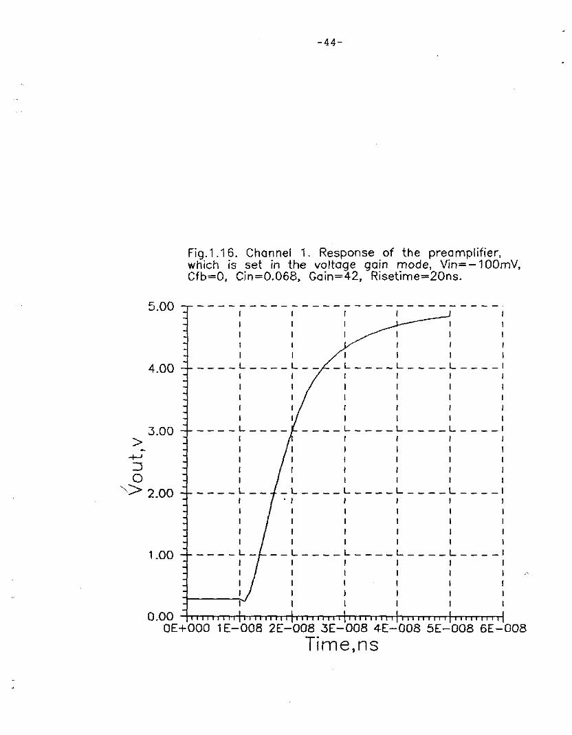
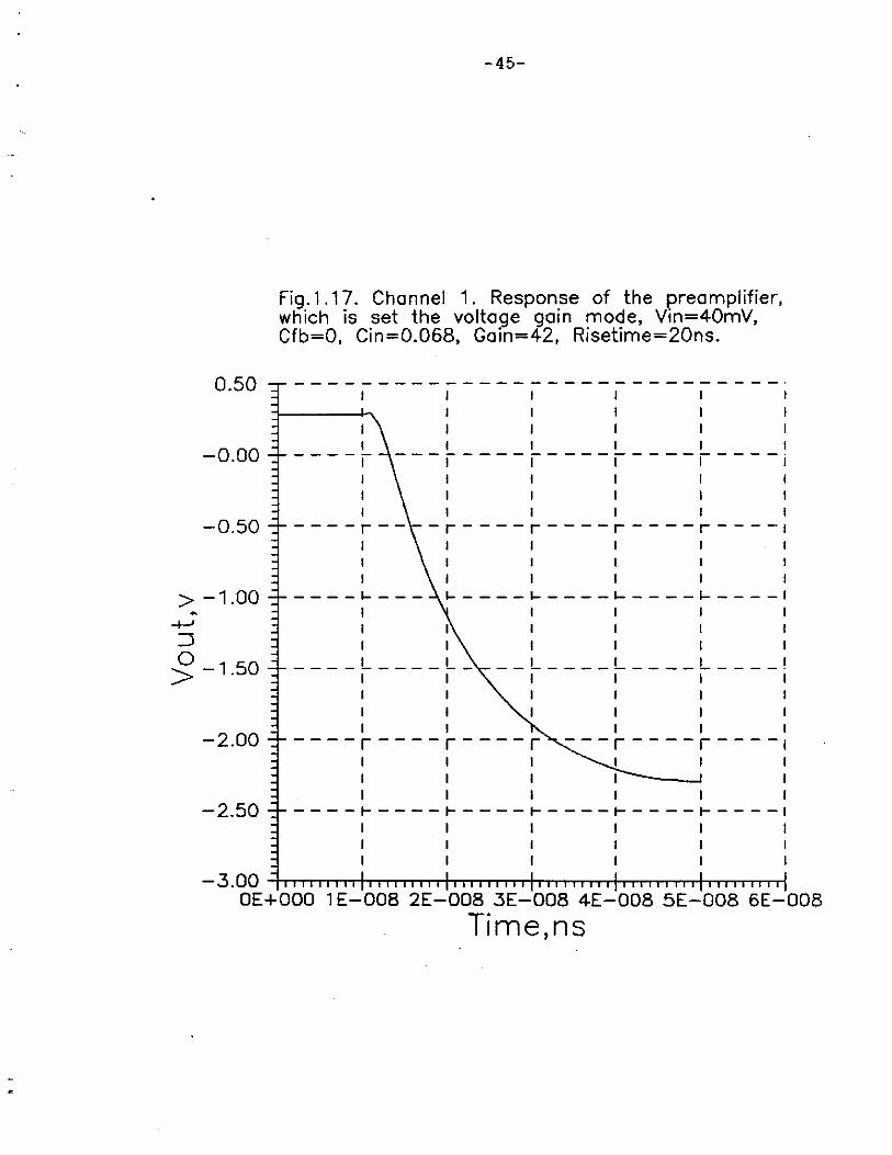
Figs.1.14, 1.1S, 1.18 and 1.19 it is seen that CSP has large speed, the pulse front edge lasts less than 10 nsec. Waveforms shown in Figs.1.16, 1.17, 1.20 and 1.21 show the gain is too low to use such a circuit for CSC muon detector application: the channel 1 has Ku= 42 and the channel 2 has Ku = 28.
1.9.9. Discrete element JFET version breadboard modelling
The charge sensitive preamplifier was modelled with discrete components on a breadboard. The electric circuit of the model is presented in Fig. 1.22. The head VTl is low noise high transconductance n-type JFET KA903A with G = SO mAIV, VT2 and VT3 are KT363U. The model has demonstrated the operability of the circuit. The front edge of the output pulse was equal 2S nsec at Cd = 220 pF, Rf = 100 kOhm, Cf = 10 pF and 100 nsec at Rf = 10 MOm and Cf = 2.2 pF. The noise measurements gav~ ENC = 900 e- at Cd = 0.
-37-.
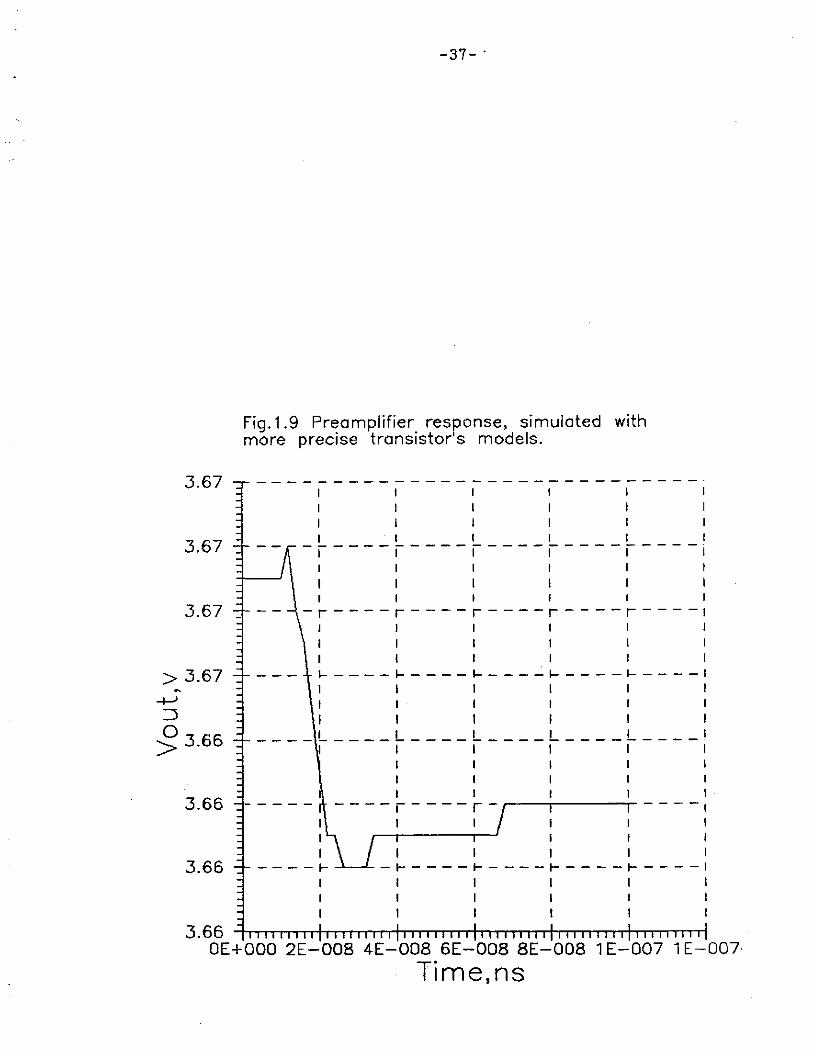
Fig. 1.9 Preamplifier response, simulated with more precise transistor's models.
367 -----------------------------· .
3.67 - - -I I I I I -1----1----1----1----1----
I I I I I I 3.67 -r----r----r----r----r----1
I
> 3.67 ~----~----~---~~----~----! I I I I I I -+-'
:::J 0 > 3.66
3.66
3.66
3.66
____ L ____ L ____ L ____ L ____ L ___ _ I I
I I - ---,- ---, -,.----.-----.-- - - -I I
I I I
- - - - I- -'-~-1- - - - - I- - - - - t- - - - - t- - - - - I I I I I I I
I I
OE+OOO 2E-008 4E-008 6E-008 BE-008 1 E-007 1 E-007
Time,ns
--4.40
-4.45
-4.50
> -
-38-
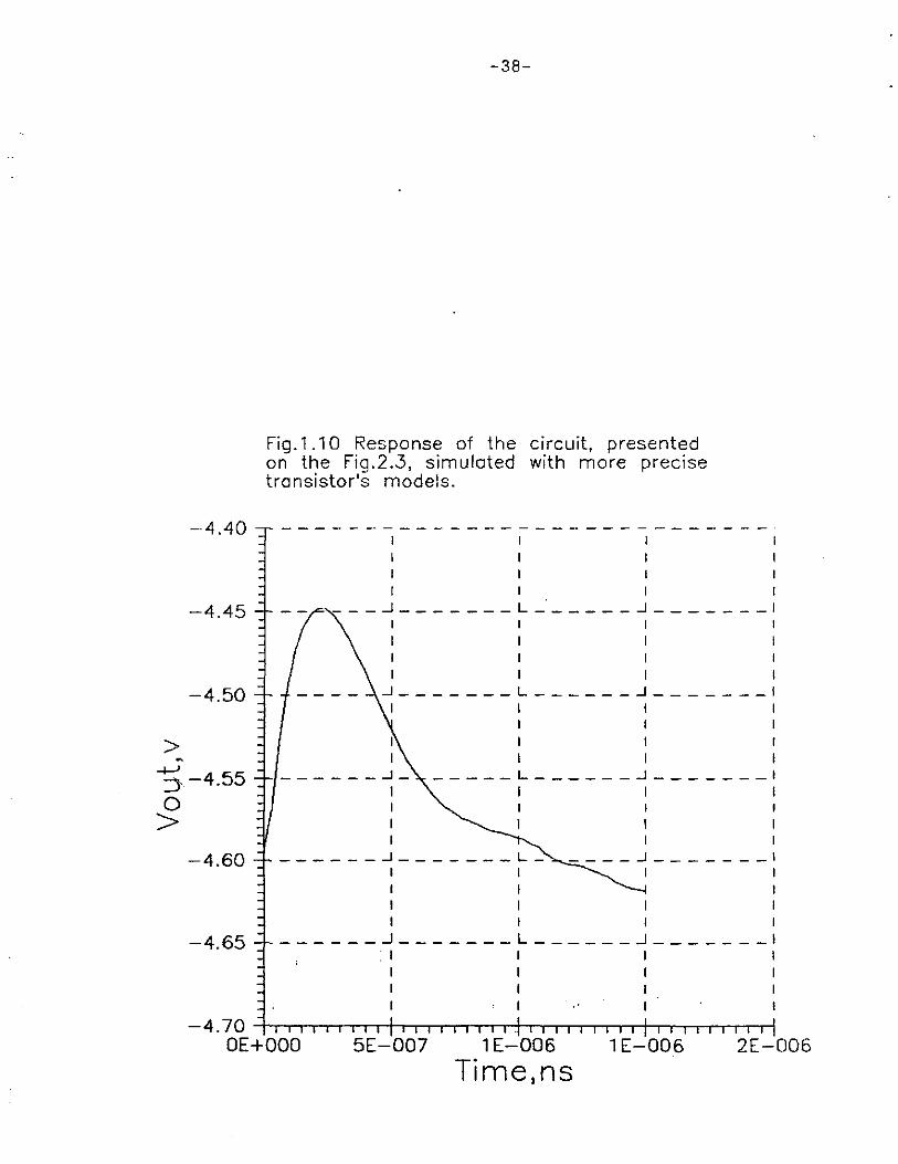
Fig. 1.10 Response of the circuit, presented on the Fig.2 . .3, simulated with more precise transistor's models.
I I I I
---~-------L~-----~-------'
I I I I
~-------L------~-------' I I I I
I
--I---' :J,-4.55 ------~- -----L------~-------'
I I I I 0 >
-4.60 ------~-------L- ----~-------' I I I I I I I I I
-4.65 ------~-------L------~-------1 _ I I I
I I
-4.70 -;-,,-,-,....,-,.--,-..--r-.-r--.--,-,-,---r-r-,-,.---,-;-,-,--,-,r-r-r-r-r-r+-r---r-r--,--r---r--r-r-rl
OE+OOO 5E-007 1 E-006 1E-006 2E-006 Time,ns

-4.74
-4.76
-4.78
> -4.80 --+-' ::J 0 > -4.82
-4.84
-4.86
-39-
Fig.1.11. Fast shaper response (simulation).
I --- - -I
I I I I -,----,----,----,----! I
I I I I I r----r----r----r----1 I I I I I
I I
----~----~----~----! I I I I .,
I L ____ L ___ L ____ L ____ L ___ _
I I
I I I ,----,----, I I
I
I I ----r----r----r----r----r----1
I I I I I I
-4.88 ...j...,.~~~i-.-.-~~~~~~i-.-.-~~~~~~h-.-~~~ DE+OOD 2E-008 4E-008 6E-008 SE-008
Time,ns 1 E-007 I 'E-007
'"

,, -· 4_0 . ..::.. . ..... r-> .
C\I -:s -~ cri J -(I> I" ('> $ ..,_ .r- ~
V) -· ('>
~su CharQQ s~nstttve pr•a•pllf1or -
n -· ., <' $;
21: UT2
-· ...,.. IH rl - •. ., UT!
3 0 "-I" -
·2.51tlp Raxt 100K
-(' .... ~ r:: . UT3
~ UH
-· tr 10r. ct- -SU s- -Cl--· .. {>
"7 \t> _,_
~] &OK
·II-:l. 9pF
~
--· r .ai:t -.:htpii!r
.---
700 l'll2
UT!! r-1 U113
~ --1~---r 10pF rtep u 1r. 2. 7K
IBK
-Slou s:h~pir
uS ~ r-
----
2K
.. rl I llT8
UTS
' ,,
' " ·~ lJT7 • IJTl0
U19
:t----
~10pf K 10K 10
-
~I 17 __ r-S.Spf
--- -·-----
1"' Outlfa£t)
Blas1ng natuort
2~K IK 21K 50K
I '!--< ~ 1enF U120
um:~ Out I UTIS -- r-- lJTl9 <slou)
I ui1s I ., ' UTIB I" UT21 .. " ~
! .BK l.H 2.B¥
--
I ..t;;~
1

R2 rk~~ 22k ---~2 >GU 22B y · ~ ~ 3, A? _l_ C3
Ci.n - - J 3n 5k7 I ----- IJT') 33n
IN 3:.9 ,J l.JTl J l<T35:lAJ L
KP903R I I KT383A OUT I \JT3
-=-::-1 C I rl R 5
I nHJ~ L lk l~ s_:k .. _G __ _i__, __ RI '/lb Tie T . -47 I ---L~!~
0lJ
RG
-8\,I
F\fb ll0k
:;J'=J Cfb l.8k
Fig. l.15. The br-eo.dboilrd model o+ the cliar·ge sensiti•Je pr-eo.rnplifiet-.

-42-
Fig.1.14. Channel 1. Preamplifier, response with Cd=O, Risetime=5ns.
040 ---------------~-------------.
I I I I I
0.20 ____ L ___ L ____ L ____ L ____ L ___ _
I
I I I I I I
000 ____ L ____ L ____ L ____ L ____ L ___ _ .
I I I
I I
I I I I >
+-' :J -0.20 ----L- __ L ____ L ____ L ____ L ___ _
I I I I 0 >
I I I
-0.40 ____ L ___ L ____ L ____ L ____ L ___ _
I I I I I I
I I I I I
-0.60 ____ L ____ L ____ L ___ ~L----L----1 I I I I
-o.so-1-r~~.......i.~~~+.-.~~...+..~~.......i.~~~-1-.-.~~~
OE+OOO 1 E-008 2E-008 3E-008 4E-008 5E-008 6E-008
Time,ns

> -+-' :J 0 >
-43-
Fig.1.15. Channel 1. Preamplifier, response with Cd= 1 OOp, Risetime= 14ns.
030 -----------------------------· .
0.20
0.10
0.00
-0.10
I I
----L-I
I
I I
--L----L----L----L----' I I I I I
----L----L----L ____ L ____ L ____ I I I I I I I I I
I I I I I I ____ L ____ L ___ L ____ L ____ L ____ I I
I I I I I I
----L----L----L----L----L----1 I I I I I I
I I
-0.20 -+..-~~...,...j.~-~+...----i...--...,...j.---.1....-.---1 OE+OOO 1 E-008 2E-008 3E-008 4E-008 5E-008 6E-008
Time,ns
-44-
Fig.1.16. Channel 1. Response of the preamplifier, which is set in the voltage gain mode, Vin= -1 OOmV, Cfb=O, Cin=0.068, Gain=42, Risetime=20ns.
5.00 - - - - - - - - - - - - - - - - - - - - - - - - - - - - - .
4.00
3.00 > -+-' :J 0
"-> 2.00
1.00
0.00
I I I I I I
----L----L--_L ____ L ____ L ____ I
1 I I I I I I
I I I I I I
----L---- ----L----L----L----1 I 1 I I I I I I
I I I I I ----L-- _L ____ L ____ L ____ L ___ _
I
----L-I
. I
I
I I I I __ L ____ L ____ L ____ L ___ _
I I I I I I I I
OE+OOO 1 E-008 2E-008 3E-008 4E-008 5E-008 6E-008
Time,ns
-45-
Fig. 1 .17. Channel 1. Response of the preamplifier, which is set the voltage gain mode, Vin=40mV, Cfb=O, Cin=0.068, Gain=42, Risetime=20ns.
050 -----------------------------· .
-0.00 I I I I I ----1 ---1----1----1----1----
1
-0.50 ----r-- -r----r----r----r----1 I I I
> -1.00 ----~--- ~----~----~----~----~ 1 I I I
+-' ::::; 0 > -1.50
____ L ____ L ___ L ____ L ____ L ___ _ I I I I I
-2.00 I I I I
----r----r----r ---r----r----
I I -2.50 ----r----r----r----r----r----1
I I I I I I
-3.00-t-rT'TTTT'TTT'i,..,.,r"T'T"r"T'T"rt'TT'T"l'TT'TTri"'T"'nrTT",..,.....ri-T.,..,...,.T'T""TTT1""T'T"1f"T'T"TTTn OE+OOO 1 E-008 2E-008 3E-008 4E-008 SE-008 6E-008
Time,ns
-0.20
-0.40
-0.60
> ~
-46-
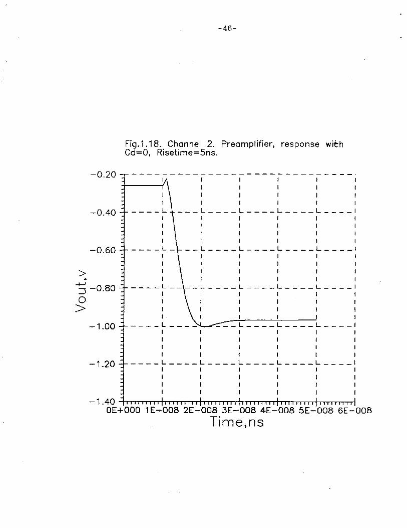
Fig.1.18. Channel 2. Preamplifier, response with Cd=O, Risetime=5ns.
I I I I I I ----L ___ L ____ L ____ L ____ L ____ I
I
I I
I I I I I I ----L- __ L ____ L ____ L ____ L ____ I
-+-' :::::; -0.BO ____ L ____ L ____ L ____ L ____ L ___ _
I I I I I 0 >
I I I I I
-1.00 ----L---- ---L----L----L----1
I I I I I I
-1.20 ____ L ____ L ____ L ____ L ____ L ___ _
I I I I I I I I I I I I
-1.40-h~~~'---~~.....1-.~~~1-.-.-~~.....1-.~~~'---~~~
OE+OOO 1 E-008 2E-008 3E-008 4E-008 5E-008 6E-008
Time,ns

-0.25
-0.30
-0.35
> -0.40 --1-' :::l 0 >-0.45
-0.50
-0.55
-47-
Fig.1.19. Channel 2. Preamplifier, response with Cd= 1 OOp, Risetime= 16ns.
-----------------------------· I I
I I I I I ----,----,----,----,----,----! I
I I I I I I
----r----r----r----r----r----1 I I I
----~--- ~----~----~----~----! I I I I
I
____ L ________ L ____ L ____ L ___ _ I I I I
I I
I I I I I ----r----r-- -r----r----r----' I
I I I ----r----r----r----r----r----
1 I I I I
-0.60 -1-.~~~i......~~...+..~~~i......~~..+.~-~i......~~....1 OE+OOO 1 E-008 2E-008 3E-008 4E-008 SE-008 6E-008
Time,ns

> --1-' :::; 0 >
-48-
Fig.1.20. Channel 2. Response of the preamplifier, which is set the voltage gain mode, Vin=-1 OOmV, Cfb=O, Cin=0.068, Gain=28, Risetime=20ns.
400 -----------------------------· .
3.00
2.00
1.00
0.00
-1.00
I I I I I ____ L ____ L __ _ ____ L ____ L ____ I
I I I ____ L ____ ----L----L ____ L ____ I
I I . I
_L ____ L ____ L ____ L ____ I
I I I I I I I
I I I I I I
----L ---L----L----L----L----1 I I I I
I I I I ____ L ____ L ____ L ____ L ____ L ____ I
I I I I I I I I I I I I I I I I I I I I
- 2. 00 -+'TTTT"rr'l-rrii-rT-rTT"l"'T'T'"rlTTTTTT"TT'T"i.......,,..,......l"'T'T'",+.-TT"T.,...,......-rf.......,,.,........,.,.,-f
OE+OOO 1 E-008 2E-008 3E-008 4E-008 SE-008 6E-008
Time,ns

-0.00
-0.50
-1.00
> ~
-49-
Fig. 1 .21. Channel 2. Response of the preamplifier, which is set the voltage gain mode, Vin=40mV, Cfb=O, Cin=0.068, Gain=28, Risetime=20ns.
I I I I I I ____ L ____ L ____ L ____ L ____ L ____ I
I I I I
----L----L----L----L----L----1 I I
I I I
I I I I ........, :J -1.50 --L----L----L----
1 I I ----L----L-
1 I 0 >
-2.00
-2.50
I I I I I ____ L - - __ L __ - - L ___ - c-..-...::-::_:-~L - - - -
I I
I I I I I I ____ L ____ L ____ L ____ L ____ L ___ _
I I I I I I I I I I I
- 3. 00 -+rrrrrrrT'TTrrrrrrTTT+r-r'rT"T'rT"TTTTTTTTTT...-rtTTT"TTT"T'T'T+r1"TT"T"T'T'T"T'1
OE+OOO 1 E-008 2E-008 3E-008 4E-008 5E-008 6E-008
Time,ns

-50-
2. PREAMPLIFIER/SHAPERS JC ELECTRONIC COMPONENT MEASUREMENTS
2.1. Purposes and content of the investigation
Two series of electronic component parameter measurements have been made to get their dependencies on BJT-JFET process parameters in operational current/voltage region, to be able to predict potential characteristics of CSP/shapers built with the technology and to modify the electronic component SPICE parameters used in the circuit computer modelling.
The first set of the component parameter measurements had been made preparatory to the first JC production iteration. For such a purpose a set of test structures I different types of a head bipolar transistor, minimal size BJT-transistors, JFETs and capacitances) has been made in a test array designed for another goals !hereinafter reffered to as 'the test array l' ITAlll.
The second set of the measurements has been made for the test structures grown together with CSP/shapers circuits on the same die, subsequently referred to as 'the test array 2' ITA2l.
To investigate the noise parameters of CMOS digital technology available at 'INTEGRAL' to estimate the possibility of its application to low noise amplifying devices production a set of MOSFETs has been made, their measurement results are reported there too.
2.2. On-wafer measurements
2.2.1. Wafers with TA1 structures
Two TA1 wafers labelled 1-6 and 1-7 have been subjected to investigation. The resistivities la surface Rsl of the next layers have been measured: • TIP - surface resistivity of p- base • T!PK - resistivity of JFET's p channel • T!G - resistivity of a deep n+ collector • T!PSS - for p+ burried layer • TlHSS - for n+ burried layer • TIEP - for epi layer • TIE - for n+ emitter • T!Z - for pJFET's n- gate r TIPP - for p+ base.
In addition values of 40 Ohm, 1 k, 10k, 50k resistors were measured.
The die yield of TAl is shown in Table 2.1.
The die yield of the TAl of investigated wafers ================================================= Wafer : Packaged dies : Fuctionally operable dies
1-6 1-7
40 50
5 28
=================================================
Table 2.1

-51-The main types of defects are the next: al for the wafer 1-6:
*short-circuit between emitter and collector of head transistors; * no connection between Si and metalJ or between metall and metal2;
bl for the wafer 1-7: • the minimal size n-p-n emitter-base short-circuits; • very fast emitter/base junction degradation after reverse biasing.
Metal problems are explained mostly by temporary unsatisfactory work of the metallisation division.
2.2.2. TA2 wafer measurements
The number of TA2 wafers to be measured equals four: 145¢-02, 145¢-05, 145¢-06 and 145¢-09. Hear we present results of measurements only for one wafer which has the lagest breackdown voltages between all the TA1/TA2 wafers as the most intreresting from the technology and circuitry point of view. Surface resistivities Rs of the process text structures, breakdown voltages of BJT junctions/JFET channels and values of all the operational resistors 10 Ohm, 0.6 k and so on to be used in circuits have been measured.
We would point out at the large depature of the base resistivity Rs=812 Ohm/sq. from the required value 550 Ohm/sq. This circumstance is supposed to magnify considerably the values of operational resistors at 45 - 70% and probably to increase a head n-p-n noise level. The relative operational resistors values disagreement appears to be explained by averaging of the resistor values being made during the measurements.
The TA2 wafer 145¢-09 die yield equals 96%. There were 48 function~lly operable dies among 50 packaged.
2.3. Packaged test structures
2.3.1. TAI structures
As the two wafers have very similar Rs in all the formed layers, we have decided to wire devices from both wafers, morever the wafer 1-6 have provided mainly JFETs. The packaged devices are listed in Table 2.2.
Table 2.2 TAI packaged devices
=================================================================== Package
Pin lDesig-: Device description : numbers : :--------------------------------------------:---------lnation:Design l Emitter/gate : Comments : c : e: bl :rule h,um:strip number n: : s : g: d:
=================================================================== 1 : 2 : 3: 4: s 6 7 8
-------------------------------------------------------------------Wafer 1-7
-------------------------------------------------------------------1 7 5 6 Ql LS 10 The head n-p-n transistors: 1 12 11 10 Q2 2.5 10 1 14 15 13 Q3 1.5 3 2 7 5 6 Q4 1.5 10 ~ 12 11 10 QS 2.5 10 ,_

-52-
=================================================================== 1 : 2 : 3: 4: 5 6 7 B
2 14 15 1 Q6 1. 5 3 3 7 5 6 Q7 1. 5 10 3 12 11 10 QB 2.5 10 3 14 15 13 Q9 1.5 3 4 7 5 6 Qll 1.5 10 4 12 11 10 Ql2 2.5 10 4 14 15 13 Q13 1. 5 3 5 12 11 10 Ql4 1. 5 10 Deep ring collector for col-
lee tor resistance Re lowering -------------------------------------------------------------------5 5
6
6 6
7
7 7 11
12 13 14
16+ 1-9 B
12 11 10
16 9
1 B
12 11 10
16 1 9 B 7 5 6
7 5 6 7 5 6 7 5 6
Cl p-n junction capacitor Cp-n, S=120x120 sq.um C2 Metal-deep collector capacitor Cmos,supposed
area 5=350•400 um
QS 1. 5 10 Head deep collector transistor
C3 Cp-n, area 120•120 sq.um C4 MOS capacitor(Cmosl, 350•400 sq.um
Q16 1.5 10 Head deep collector transistor
cs Cp-n, s = 120•120 sq.um C6 Cmos, s = 350•400 sq.um Q20 1. 5 1 Minimum size n-p-n,
emitter 1.5•4.0 um Q21 1.5 1 Minimum size n-p-n Q22 1. 5 1 Minimum size n-p-n Q23 1. 5 1 Minimum size n-p-n
--------------------------------------------------------------------1 : 2 . ... 4: 5 6 7 B ' ~·
Wafer 1-6
B 7 5 6 Q17 1.5 15 Head n-p-n transistor 8 1 2 B Jl 1.5 1 pJFET, width 20 um B 15 16 9 J2 1.5 2 pJFET, width 30 um B 14 13 12 11 J3 1.5 Two-gate pJFET, pin 14-upper
gate, 12-down gate, 13-source 9 7 5 6 Q18 1.5 15 Head n-p-n transistor 9 1 2 8 J4 1.5 1 pJFET, width 20 um 9 15 16 9 JS 1.5 2 pJFET, width 30 um 9 14 13 12 11 JS 1.5 Two-gate pJFET 10 7 5 6 Q19 1.5 15 Head n-p-n transistor 10 1 2 B J7 1.5 1 pJFET, width 20 um 10 15 16 9 JB 1. 5 2 pJFET, width 30 um 10 14 13 12 11 J9 1.5 Two-gate pJFET ================================================================

-53-
2.3.2. TA2 structures
The next TA2 electronic devices types were packaged: • a head n-p-n transistor having a design rule h=l.5 um, a number
of emitter strips n=10 and a structure with a deep ring collector !collector - pin 10, base - 11, emitter - 121
• pJFET with the two gates being connected !Version 1, source - 15, drain - 13, gate - 141
• pJFET with the two separate gates, an upper gate has a strip form like the Tektronix type JFET !Version 2, d-7, s-5, down gate - 8, upper gate - 6
• pJFET with the two separate gates, an upper gate has a ring form like the Analog Devices type JFET !Version 3, s-4, d-2, ug-3, dg-161.
The ring gate pJFET is supposed to possess the least possible flicker noise value, but it has very low yield now which is supposed to be explained by difficulties in making 1.5 um gap in the tilled parts of the layout.
2.3.3. Test capacitance measurements ITAl structures)
All the test capacitances Cl - C6 have been measured by impedancemeter E7-12. Summary straw capacitance of a test socket and package was subtracted from the measured values. Contact pad stray capacitances were neglected since contact pad metal is deposited on a thick oxide insulating layer about 1.5 um. The dependance of the mean capacitance values on reverse bias voltage V rev are shown in Table 2.3.
Table 2.3 Mean test capacitor values versus reverse bias voltage
================================================================= V rev, v: 0 1. 0 2.0 3.0 4.0 5.0 10.0
Cp-n, pF: 3.78 : 2.76 2. 36 : 2. 12 : 1. 96 : 1. 83 : 0.71
Cmos, pF: 20.09: 19.95 =================================================================
2.4. n-p-n transistor measurements
2.4.1. Static parameters of TAl n-p-n test structures
To measure test n-p-n transistor static characteristic the transistors with breakdown voltage Vee> 8.0 Vat lb= 0 · and leakage current 10 uA were selected. The measurements were made with transistor-and-diode tester i2-70. There are averaged junctions breakdown voltages shown in Table 2.4, where Vee - collector-emitter breakdown voltage with base being uncon
nected, lb = O; Veb emitter-base breakdown voltage; Vbc - collector-base breakdown voltage.

-54-
All the breakdown voltages were measured with a transistor-and-diode tester i2-56 at leakage current 10 uA. Averaged dependencies of static common-emitter current gain on <h21E>, typical individual h21E and difference gain h21e for the tested trans is tors are shown too, where
Jc : die : h21E = ' ' . h21e =
lb :Uce=Const dlb :uce=Const
Table 2.4 Static TAl n-p-n characteristics
===================================================================== le, mA ---> :o.1:0.3:o.5:i.0:2.0:5.o: 10: 30: 50
Sample :operation : Breakdown :volt. /---: voltage, V Ucb,V/ h21 :Veb: Vcb: Vee:
--------:---:------:---:----:----:---:---:---:---:---:---:---:---:---1 : 2 : 3 : 4 : 5 : 6 : 7 : 8 : 9 : 10: 11: 12: 13! 14: 15
--------:---:------:---:----:----:---:---:~--:---:---:---:---:---:---
II af er 1-7 --------:---:------:---:----:----:---:---:---:---:---:---:---:---:---Q6 3.0<h21E> 5.8 20.0 11. 5 258 25S 247 238 221 171 132 69 51 h= 1. Sum 1. 0 h21E 199 193 188 182 179 149 128 66 34
1.0 h21e 185 184 178 168 153 124 98 29 15 n=3 3.0 h21E 219 215 207 194 177 140 109 48 20 Ua=13.1V! 3.0 h21e 238 230 221 212 198 171 144 86 48 --------:---:------:---:----:----:---:---:---:---:---:---:---:---:---Q4 3.0 <h21E>5.8 19.0 11.7 215 228 228 229 224 201 167 107 84 h=1.5um : 1. 0 h21E 150 160 162 163 161 155 146 119 100 n=lO 1. 0 h21e 154 166 164 162 158 144 130 93 66 Ua=14.5V: 3.0 h21E 169 184 185 187 187 177 167 136 116
3.0 h21e 176 189 188 186 180 163 147 106 83 --------:---:------:---:----:----:---:---:---:---:---:---:---:---:---Q14,n=10: 3.0 <h21E>5.8 19.5 11. 5 265 261 255 239 221 180 146 102 81 h= 1. Sum : LO h21E 224 222 217 210 200 151 110 65 Ua=9.9V•: 1.0 h21e 210 211 208 200 158 106 67 40 Deep ring 3.0 h21E 283 275 267 257 238 167 121 78 54 collector 3.0 h21e 262 260 255 241 178 158 114 48 30 --------:---:------:---:----:----:---:---:---:---:---:---:---:---:---Q5 3.0 <h21E>5.8 19.0 11. 9 363 326 307 306 280 272 251 181 h=2.5um ' 1.0 h21E 244 227 220 213 203 190 151 137 120 ' n=10 1.0 h21e 209 212 208 202 196 175 146 109 95 Ua=11.1V: 3.0 h21E 347 285 271 258 243 228 211 170
3.0 h21e 257 256 248 240 224 205 183 133 111 --------:---:------:---:----:----:---:---:---:---:---:---:---:---:---
Wafer 1-6 --------:---:------:---:----:----:---:---:---:---:---:---:---:---:---Q18 :3.0 <h21E> 5.8 22.0 12.8 205 211 h=1.5um : 1.0 h21E 183 186 n=15 l 1. 0 h21e 180 186 Ua=18.2V!3.0 h21E 211 214
!3.0 h21e 206 212
210 209 205 202 185 183 181 171 184 181 177 161 211 209 202 197 211 205 198 190
178 164 150 160 128
184 150 135 116 109 80 134 134 126 100
===================================================================== * Ua - Early's voltage
<h2lE> - averaged value

-55-
2.4.2. Static parameters of TA2 test n-p-n transistors
The test n-p-n transistors were measured with the next testers: * TR-4805 * i 2-70
!breakdown voltages !h21E, h21e, Ual !Ftl
Veb, Vcb and Vcel
* i 2-68 • E7-12 !Ccb, Cbe, Ccsl .
The measuremrnts results are shown in Tables 2.5 and 2.6.
Table 2.5. Static TA2 test n-p-n characteristics !h=l.5 um, n=lO, ring deep col lectorl
===================================================================== Sample
le, mA ---> :o.1:0.J:o.s:1.0:3.o: s.o: 10
!Operation: Straw capa-: :volt. /--: citances, pF\ Ucb,V/h21/ Ccs: Ccb: Cbe:
50
----------:---:----:----:----:----:---:---:---:---:---:----:----:----1 : 2 : 3 : 4 : 5 : 6 : 7 : 8 : 9 : 10: 11: 12 : 13 : 15
----------:~--:----:----:----:----:---:---:---:---:---:----:----:----NlO 1.0 h21E 2. 37 2.04 1.45 102 104 103 102 88 78 53 24 Ua =16.63V 3.0 h21E 118 119 118 113 97 86 60 34 Vcb=24.0 v 1. 0 h21e 100 103 102 92 74 54 33 15 Vbe= 5.9 v 3.0 h21e 115 118 117 102 80 64 36 20 Vee= 11. 4 v ----------:---:----:----:----:----:---:---:---:---:---:----:---:-----N16 1. 0 h21E 2.26 1. 94 1. 43 82 85 86 85 70 56 41 20 Vcb=24.5 v 3.0 h21E 86 92 92 91 74 60 49 24 Vbe= 6.0 v 1.0 h21e 87 89 86 80 56 36 21 11 Vce=12.4 v 3.0 h2.le 94 96 94 83 63 37 28 22 Ua=l6.8 v ----------:---:----:----:----:----:---:---:---:---:---:----:----:----N14 1.0 h21E 2.22 !. 93 1. 45 71 74 75 70 69 60 50 26 Ua= 16. 2 v 3.0 h21E 76 78 84 80 74 68 53 36 Vcb=19.0 v 1.0 h21e 74 76 83 80 57 43 32 16 Vbe= 6.0 v 3.0 h21e 78 82 86 91 70 45 36 24 Vce=12.2 v ----------:---:----:----:----:----:---:---:---:---:---:----:----:----N20 1. 0 h21E 2.23 1.89 1.47 93 96 97 97 95 75 52 25 Ua= 17.2 v 3.0 h21E 107 110 110 108 94 83 60 33 Vcb=21. 0 v 1.0 h21e 98 98 97 90 72 52 36 14 Vbe= 6.0 v 3.0 h21e 106 110 111 100 78 64 38 32 Vce=ll.8 v ----------:---:----:----:----:----:---:---:---:---:---:----:----:----
Table 2.6 TA2 test.n-p-n transistor stray capacitances dependence on a reverse bias voltage
===================================== Ureu, V : 0 l 1.0 l 3.0 : 5.0 --------:------:------~------~------: Ccb, pF 1. 93 1.53 1.24 1.13 Cbe, pF : 1.45 l 1.17 : 0.87 : 0.79 : Ccs, pF : 2.22 l 1. 79 l 1.51 : 1.40 : ========!======:======\======:======:

-56-
2.4.3. Ft measurements of TA1 structures
Unit gain frequency Ft was determined by measurements of /h21e/ at high frequencies Fm:
Fr = /h21el•Fm
A transistor-and-diode tester !2-68 to be used for the measurements can measure lh21el <=32 at Fm= 100 kHz, i.e. we were able to measure Ft up to 3.2 GHz. Transistors with lager Ft up to 9.0 GHz should be packaged to four pin 'helicopter-type' pacage. To test a large number of transistors with Ft < 3.2 GHz during this test we were forced to set our test devices to 16 pin micropackage H01.16-1b. Contact adapter test sockets of used tester can measure the package of this type at frequency not more than 100 MHz.
The measurement results are shown in Table 2. 7. It is seen that some n-p-n samples demonstrate Fr > 3.2 GHz, so at the next stages the Ft measurements are supposed to be made with adequate packaged devices.
It should be noted that the results have shown good repetitity for the same device type from package to package. Ft dispersion appears to be less than 2%, which is no more than the measurement char.nel error of the testor itself.
Table 2.7 TA1 test n-p-n Ft estimates versus emitter current
=================================================================== : re, mA: O. 1: o. 3: o. 5: 1 : 3 5 : 10 : 30 : 50
Sample :======:---:---:---:---:----:-----:-----:-----:-----\ Ucb,V! Ft, MHz
----------------\-----:---:---:---:---:----:-----:-----:-----:-----Q6, h=l.5um, jj =3
: 1.0 1119 324 530 936 2430 >3200 >3200 1290 : 3.0 :120 327 532 943 2490 >3200 >3200 2530
681 983
----------------:-----:---:---:---:---:----:-----:-----:-----:-----~4, h::::1.5um, n=10
: 1.0 : 92 248 396 681 1600 2210 2290 >3200 3010 : 3.0 : 94 254 406 704 1690 2360 >3200 >3200 >3200
----------------:-----:---:---:---:---:----:-----:-----:-----:-----QS, h::.2.5, n=!O
: 1.0 : 89 249 404 698 1650 : 3.0 : 87 244 405 712 1740
2260 2430
3120 >3200 >3200 3180 >3200 >3200
----------------:-----:---:---:---:---:----:-----:-----:-----:-----Q18, h=l.5, n=15
: 1.0 : 82 214 338 613 1280 : 3.0 : 83 222 352 603 1380
1720 1890
2280 2570
2660 3170
2210 3100
----------------:-----:---:---:---:---:----:-----:-----:-----:-----Q14,rlng deep c.: 1.0 : 97 264 429 748 1810 h=l.5, n=10 : 3.0 : 98 269 437 771 1910
2510 >3200 2660 >3200
3190 >3200 3190 >3200
=====::.================~============================================
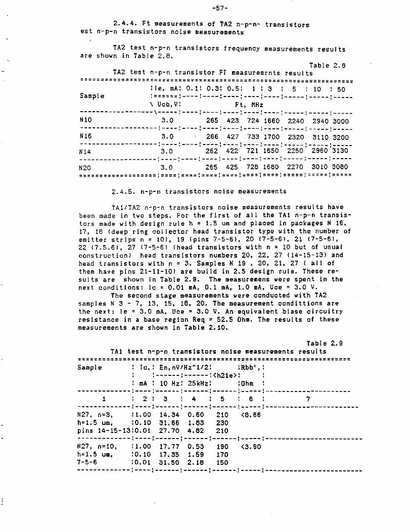
-57-
2. 4. 4. Ft measurements of T·A2 n-p-n- trans is tors est n-p-n transistors noise measurements
TA2 test n-p-n transistors frequency measurements results are shown in Table 2.8.
Table 2.8 TA2 test n-p-n transistor Fr measuremrnts results
=================================================================== : le, mA: 0.1: 0.3: 0.5: 1 : 3 5 : 10 : 50
Sample :======:----:----:----:----:----:-----:-----:-----\ Ucb,V: Ft, MHz
------------------\-----:----:----:----:----:----:-----:-----:-----NlO 3.0 265 423 724 1660 2240 2940 3000 -------------------:----:----:----:----:----:----:-----:-----:-----N16 3.0 266 427 733 1700 2320 3110 3200 -------------------:----:----l----:----:----:----:-----:-----:-----N14 3.0 262 422 721 1650 2250 2960 3130 -------------------:----:----:----:----:----:----:-----:-----:-----N20 3.0 265 425 728 1680 2270 3010 3080 ===================:====:====:====:====:====:====:=====:=====:=====
2.4.5. n-p-n transistors noise measurements
TA11TA2 n-p-n transistors noise measurements results have been made in two steps. For the first of all the TAl n-p-n transistors made with design rule h = 1.5 um and placed in packages N 16, 17, 18 !deep ring collector head transistor type with the number of emitter strips n = 10), 19 !pins 7-5-6l, 20 !7-5-6l, 21 !7-5-6l, 22 !7.5.61, 27 l7-5-6l !head transistors with n = 10 but of usual construction) head transistors numbers 20, 22, 27 !14-15-13) and head transistors with n = 3. Samples N 19 , 20, 21, 27 l all of them have pins 21-11-lOl are build in 2.5 design rule. These results are shown in Table 2.9. The measuremens were spent in the next conditions: le= 0.01 mA, 0.1 mA, 1.0 mA, Uce = 3.0 V.
The second stage measurements were conducted with TA2 samples N 3 - 7, 13, 15, 18, 20. The measurement condittions are the next: le= 3.0 mA, Uce = 3.0 V. An· equivalent biase circuitry resistance in a base region Req = 52.5 Ohm. The results of these measurements are shown in Table 2.10.
Table 2.9 TAl test n-p-n transistors noise measurements results
=================================================================== Sample le,: En, nV/Hz"'112! IRbb',:
:------:------:<h21e>l mA : 10 Hz: 25kHz: :ohm
-------------:----:------:------:------:-----:---------------------1 2 : 3 4 5 6 7
-------------:----:------:------:------:-----:-----------------------N27, n=3, : 1. 00 h=l.5 um, :0.10 pins 14-15-13:0.01
14.34 31. 66 27.70
0.60 1.83 4.82
210 230 210
<8.66
-------------:----:------:------:------:-----:------------------------N27, n=lO, h=l.5 um, 7-5-6
: 1.00 :0.10 :0.01
17.77 17.35 31.50
0.53 1.59 2.18
190 170 150
<3.90
-------------:----:------:------:------.:-----:------------------------

-58-
-------------:----:------:------:------:-----:---------------------1 2 : 3 4 5 6 7
-------------:----:------:------:------:-----:-----------------------N=22, n=3, h=l.5 um, 14-15-13
: 1.00 :o. 10 :0.01
28.82 31. 24 39.81
1. 9 2.24 2. 18
210 230 210
192.0
-------------:----:------:------:------:-----:------------------------N=22, n=lO, h=l.5 7-5-6
: 1. 00 :OslO :o. 01
<11. 66 11. 35 44.66
1. 00 1.50 3.39
190 170 150
35.3
-------------:----:------:------:------:-----:------------------------N21, n=lO, h=l.5 um, 7-5-6
: 1.00 0.10 0.01
11. 0 18.83 22.38
0.71 1. 59 4.82
190 170 150
5.4
-------------:----:------:------:------:-----:------------------------N20, n=3, h=l.5 um, 14-15-13
1. 00 0.10 0.01
39.88 19.3 25.7
2. 15 1. 59 4.71
190 170 150
78.3
-------------:----:------:------:------:-----:------------------------N20, n=10, h=l.5 um, 7-5-6
: 1. 00 :o. 10 :0.01
39.88 19.30 25.70
2. 15 1. 59 4.71
190 170 150
-------------:----:------:------:------:-----:--------~---------------N19, n=lO, h=l.5 um, 7-5-6
: 1. 00 : o. 10 :0.01
41.40 2.44 39.85 11.17
190 170
-------------:----:------:------:------:-----:------------------------N=27, n=10, h=2. 5 um, 12-11-10
: 1.00 :0.10 :o. 01
16.40 29. 15 31. 62
0.82 0.86 5.30
240 320 300
16. 1
-------------:----:------:------:------:-----:------------------------N=21, n=lO, h=2.5 12-11-10
: 1. 00 :0.10 :0.01
44.13 19.93 39.80
0.67 1.50 3.59
240 320 300
2.1
-------------:----:------:------:------:-----:------------------------N20, n=10, h=2. 5 um, 12-11-10
: 1. 00 0.10 0.01
13.31 63.07 56.21
0.89 1. 64 3.98
240 320 300
22.8
-------------:----:------:------:------:-----:------------------------N19, n=lO, 1.00 29.16 1.02 240 37.8 h=2.5 um, 0.10 38.90 1.45 320 12-11-10 0.01 31.60 300 ::-~-----------:~---:------:------:------:-----:------------------------N=16, n=10, h=l.5 um, 12-11-10
: 1. 00 125. 89 :0.10 63.09 :0.01 100.00
1.08 2.39 8.55
250 270 240
Ring deep collector
------------- ----:------:------:------:-----:------------------------N=17, n=lO, h=l. 5 12-11-10
1.00 0.10
25.11 28.16
1.42 3.91
250 270
Ring deep collector
------------- ----:------:------:------:-----:------------------------N 18, n= 10, h=l.5 um, 12-11-10
1.00 0.10 0.01
19.95 34.48
1.10 4.69
250 270
Ring deep collector
=============:====:======l======:======:=====l=======================
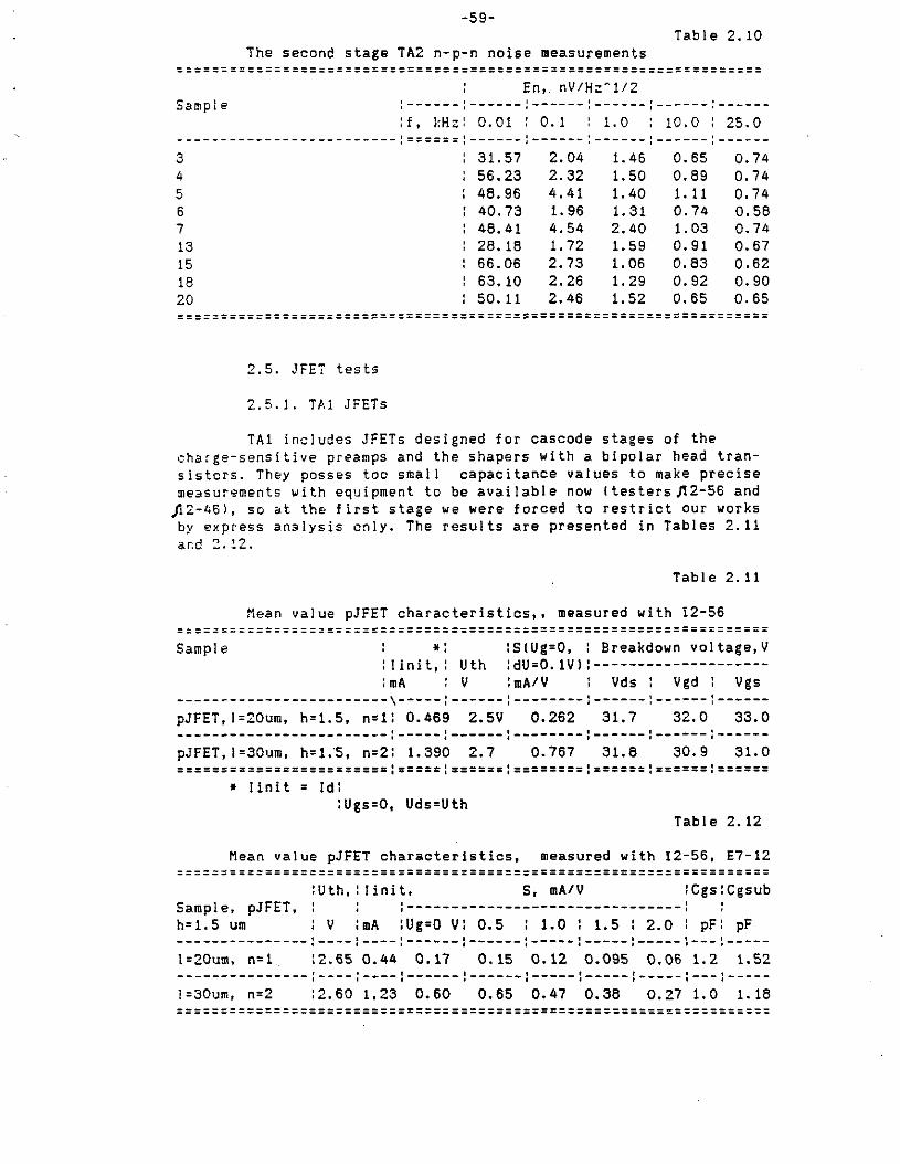
-59-Table 2.10
The second stage TA2 n-p-n noise measurements ==================================================================
En, nVIH="l/2 Sample :------:------:------:------:------:------
:f, kHz: 0.01 : 0.1 1. 0 10.0 : 25.0 -------------------------:======:------:------:------:------ ------3 31. 57 2.04 4 56.23 2.32 5 48.96 4.41 6 40.73 1. 96 7 48.41 4.54 13 28. 18 1. 72 15 66.06 2.73 18 63. 10 2.26 20 50. 11 2.46
1. 46 1. 50 1. 40 1. 31 2.40 1.59 1. 06 1. 29 1. 52
0.65 0.89 1. 11 0.74 1. 03 0.91 0.83 0.92 0.65
0.74 0.74 0.74 0.58 0.74 0.67 0.62 0.90 0.65
=======================================~===========================
2.5. JFET tests
2.5.l. TAI JFETs
TA! includes JFETs designed for cascade stages of the charge-sensitive preamps and the shapers with a bipolar head transistors. They posses too small capacitance values to make precise :neasurements with equipment to be available now ttesters )l2-56 and
Ji2-46), so at the first stage we were forced to restrict our works by express analysis only. The results are presented in Tables 2.11 ar.d ~. !2.
Table 2.11
Mean value pJFET characteristics,, measured with i2-56 =================================================================== Sample
:Jinit,: Uth : mA : V
:s1ug=O, : Breakdown voltage,V :dU=0.1Vl:--------------------:mAIV Vds : Vgd : Vgs
------------------------\-----:------:--------:------:------:------pJFET, 1=20um, h=1.5, n•1: 0.469 2.5V 0.262 31. 7 32.0 33.0 ------------------------:-----:------:--------:------:------:------pJFET, 1=30um, h=1;s, n=2: 1.390 2. 7 0.767 31.8 30.9 31.0 ========================:=====:======:========:======:======:======
• linit = Id: :ugs=O, Uds=Uth
Table 2.12
Mean value pJFET characteristics, measured with i2-56, E7-12 ===================================================================
:uth,:Iinit, S, mA/V :cgs:Cgsub Sample, pJFET, :-------------------------------: h= 1. 5 um : V :mA :Ug=O V: 0.5 : 1. 0 : 1. 5 : 2. 0 : pF: pF ---------------:----:----:------:------:-----:-----:-----~---:-----l =20um, n= 1 :2.65 0.44 0.17 0.15 0.12 0.095 0.06 1.2 1.52 ---------------:----:----:------!------:-----:-----:-----:---:-----l =301Jm, n=2 :2.60 1.23 0.60 0.65 0.47 0.38 0.27 1.0 1.18 ===================================================================

-60-
2.5.2. TA2 test JFET static characteristics measurements
pJFET static characteristics, namely the dependences of a drain current Id on a gate-source voltage Ugs at a fixed drain-source voltage Uds = 3 V, were determined by a tester TR-4805, and in the process a down gate of Versin 2/3 pJFET was biased by a constant reversed voltage Ubgs = 0, 1.0, 2.0, 3.0 V, taken from an external voltage supply. An output difference resistance and parameter L'-1 !1/lambdal were determined by TR-4805 too. Junction capacitances were measured by E7-12.
Current-voltage characteristics are assumed to satisfy the next equation:
le= Bil+ LUdsllUth - Ugsl'2 12. 1)
at Uds > Uth - Ugs 12.2)
To get the model parameter B from eq. !2.1 l we should neglect L and fix Ugs = 0. Then we have
Id 81 = -----: ( 2. 3)
Uth'2:Ugs=O
Bl estimate precision is seen from 12.31 to be determined by Id and Uth measurement accuracy with the latter having the greatest error being measured any one of testers i2-56, Aaol-1 or TR-4805. So B may be calculated from the next equation:
!ld2l'l/2 - lldll'l/2 '1/2 12.4) B2 = [---------------------)
Ugs2 - Ugsl at Uds=Const=3. 0 V,
where ld2, ldl - drain currents at voltages Ugsl and Ugs2 respectively and at fixed Uds.
With known B2 we can calculate Uth
Uth = Ugsl + !ld1/B2l'1/2, ( 2. 5)
where ldl - drain current at Ugsl and fixed Uds = Const·= 3.0 V, and pJFET transconductance in its ~ependence on the drain current
did s = = 2 IB2• ld l '112 ( 2. 6)
dUgs
The pJFET unit gain frequency is determid to be
Ft = s1z§csum, 12. 7l
where Csum - the total capacitance connected to the gate, er,- - 3. 14.

-61-
For version 1 pJFET we have
Ft = S/2~!Cgsb + Cgs I. 12. 8)
The versions 2, 3 unit gain frequency equals
Ft = SIZ'»Cgs (2. 91
Measured and calculated according eq. 2.3 - 2.9 parameters are shown in Tables 2.13, 2.14.
Table 2.13 TA2 test pJFET static characteristics measurement results
=================================================================== Udngs: !d!Uds=3.0l,mA:Uth:L·-i: Bl, 82, :S!Uds=3.0VlmA/V
:----:----:----: ----:----:-----Sample: :Ugs=:Ugs=:Ugs=: mA/ mA/ 0.2 : 1.0 : max. N, pins v :o v :o.sv:1.ov: v v 1v·2:1v·2 mA ' mA ' ' ' -----------:----:----:----:----:---:----:-----:---- ----:----:-----
1 ' " 3 ' 4 ' 5 ' 6 ' 7 ' 8 9 10 ' 11 : 12 ' ~ ' ' ' ' ' ' -----------:----:----:----:----:---:----:-~---!---- ----:----1-----
Version 1 pJFETs N17,15-14-13 15.0 10. 1 5.8 2.5 24.3 2.400 2. 14 1. 31 2.93 11.33 N6, 15-14-13 15.0 10. 1 6.0 2.5 23.3 2.400 2. 14 1. 31 2.93 11. 33 NlO, 15-14-13 16. 9 11.2 6.7 2.5 22.9 2.704 2.28 1.35 3.01 14.40 N4, 15-14-13 17. 1 11. 8 7. 1 2.5 23.1 2.736 2.09 1. 29 2.89 11. 96 N3, 15-14-13 19.3 13.5 8.4 2.6 19. 1 2.855 2.24 1. 34 2.99 13. 15 N19,15-14-13 18.9 13.3 8.3 2.6 20.5 2.800 2.15 1. 31 2.91 11. 32 -----------:----:----:----: Version 2 pJFETs :----~----:-----N 19. 5-6-7 o.o 9.0 7.5 6.2 5.5 30.0 0.297 0.26 0.45 1. 02 3.06
1.0 7.2 5.8 4.3 4. 1 0.37 0.54 1.22 3.29 2.0 5.4 4.0 2.7 3.3 0.46 0.60 1. 36 3.16 3.0 3.8 2.5 1. 4 2.3 0.59 0.68 1. 53 3.00
N 1, 5~6-7-8 0.0 7.5 6. 1 4.9 5.0 30.0 0.300 0.27 0.47 1. 05 2.89 1.0 5.7 4.4 3.2 3.3 0.35 0.53 1. 20 2.85 2.0 4.2 2.9 1. 8 2.6 0.50 0.63 1. 41 2.89 3.0 2.8 1. 7 0.7 2.0 0.70 0.75 1. 67 2.80
N? -· 5-6-7-8 0.0 7.4. 6.2 5.0 4.8 29.6 0.328 0.23 0.43 0.96 2.62 1.0 5.8 4.4 3.2 3.3 0.35 0.53 1. 18 2.83 2.0 4.3 3.0 1. 9 2.5 0.48 0.62 1. 39 2.88 3.0 3.0 1. 7 0.8 2.0 0.70 0.74 1. 68 2.90
NB, 5-6-7-8 o.o 8.0 6.7 5.4 5.0 26.7 0.320 0.27 0.47 1.05 2.89 1.0 6.4 5.0 3.7 3.8 o. 37 0.55 1.22 3.09 2.0 4.7 3.4 2.2 2.8 0.47 0.62 1.38 2.98 3.0 3.4 2.0 1. 1 2.2 0.63 o. 71 1.59 2.93
-----------:----:---:----: Version 3 pJFET :----:----:----N3,2-3-4-16 0.0 9.0 7.6 6.3 5.5 25.7 0.298 0.24 0.44 0.98 2.93
1.0 7.4 5.7 4.4 4.1 0.39 0.56 1.24 3.38 2.0 5.5 4. 1 2.8 3.3 0.46 0.60 1. 35 3. 16 3.0 4.0 2.6 1.4 2.5 0.57 0.73 1. 64 3.27
N18, 0.0 7.4 6. 1 4.9 5.0 29.6 0.296 0.26 0.46 1. 02 2.77 2-3-4-16 1.0 5.8 4.4 3.2 3.8 0.38 0.55 1.24 2.98
2.0 4.2 2.9 1. 8 2.6 0.50 0.63 1. 42 2.9! 3.0 2.8 1. 6 0.7 ---:----:-----:----:----:----:----
NL:., 0.0 8.0. 6.6 5.3 5.0 29.1 0.320 0.28 0.47 1.06 2.99 :-3-~-16 !.O 6.3 5.0 3. 7 3.8 0. 35 0.53 l. 18 2.. 96
::. 0 4.8 3.3 2.1 2.8 0.55 0.66 1.48 3.24 3.0 3.3 2.0 1.0 2.0 0.67 0.73 1. 63 :. 97
===========:====:====:====:====:===:====:=====!====:====:====:====

-62-
Table 2.14 TA2 test pJFET unit gain frequency measurement results
================:================================== :Udgs:<Cgs>:<Cgd>:<Cgsb>:Uth:Uth,V: Ft
:cal cu-Sample : lated:
v pF pF pF V ? MHz: -----------:----:-----:-----~------:---:-----:----:
1 : 2 3 4 5 : 6 : 7 6 : -----------:----:-----:-----:------:---:-----:----: 17' 15-14-13 6, 15-14-13 10,15-14-13 4, 15-14-13 3, 15-14-13 14,15-14-13
Version 1 pJFETs 9.27 9.20 5.78 2.5
2.5 2.5 2.5 2.6 2.6
2.65 2.65 2.72 2.66 2. 93 2.96
120 120 152 127 139 120
-----------:----: Verion 2 pJFETs ---:-----:-----19, 5-6-7 6
o.o 1. 0
3.12 3.10 157 5.5 5.68
Nl, 5-6-7-8
2.0 3.0 0.0 1.0 2.0 3.0
N2, 5-6-7-6 0.0 3.12 3.10 1. 0 2.0 3.0
NB, 5-6-7-6 ·o. 0 1.0 2.0 3.0
-----------:----: N3,2-3-4-16 0.0
1. 0 2.0 3.0
N16, 0.0 2-3-4-16 1.0
2.0 3.0
N4, O. O 2-3-4-16 1. 0
2 •. 0 3.0
Ver ion 3 pJFET 3.49 3.55
4.1 4.38 3.3 3.41 2.3 2.53 5.0 2.56 147 3.3 3.99 2.6 2. 90 2.0 2.00 4.8 5.66 133 3.3 4.09 2.5 2.99 2.0 2.07 5.0 5.57 146 3.8 4.15 2.8 3.15 2.2 2.32 ----:----:-----5.5 4.1 3.3 2.5 5.0 3.8 2.6
5.0 3.8 2.8 2.0
6.12 4.36 3.47 2.44 5.33 3.89 2.89
5.33 4.25 2.95 2.22
137
126
136
=====~=====:====:=====:=====:======:====!====!=====
2.5.3. TA2 test JFET noise measurements
Noise levels were measured for all the three versions of the TA2 test JFETs. The results are shown in tables 2.15 - 2.17.

-63-
Connected gate !Version 11 pJFET Table 2.15.
noise !Uds = 3.0 Vl ==================================================================
En, nV/Hz' 112 Version 1 samples :------:------:------:------:------:------
: ft kHz: 0.01 ' o. 1 1.0 10.0 ' 25.0 ' ' ------------------------- ======:------:------:------:------:------
Id, mA: 3 19.3 31.15 15. 64 4.46 1. 99 1. 99 4 17. 1 29. 17 6.51 2.31 1. 75 1. 60 5 17. 4 46. 77 16.40 3.75 1. 77 1. 75 6 15.0 35.46 15.64 7.07 3. 16 3.16 7 17.3 32.73 7.41 3.31 1. 99 1. 99 10 16. 9 46.77 10.47 3.93 1. 64 1. 64 13 16.2 30.01 16.76 5.75 3.31 2.69 15 17. 9 27.22 7.94 3.63 2.37 1. 99 16 16.0 46.77 10.23 2.29 2. 11 1. 54 =========================:======:======:======:======:======:======= Gate biasing circuit spectral density !calculated), nV/Hz'l/2 : 1. 33 ====================================================================
Double-gate !Version 21 pJFET Table 2.16.
noise !Uds = 3.0 VI ==================================================================
:Down En, nV/Hz' 112 Version 1 samples :gate v,------:------1------:------:------:------
:Udgs,V:f, kHz: 0.01 : 0.1 1.0 10.0: 25.0 ---~--------------:------!======:------:------:------:------:------
4 0.0 2.0
Id, mAl 7.6 4.4
72.26 56.23
20. 16 15.46
6.91 5.62
4. 16 2.63
3.31 2.63
------------------:------:------:------:------:------:------:------5 0.0
: 2.0 6.5 69.12 5. 0 : 75 •. 65
27.66 14.79
6.70 6.09
4. 37 3.96
4.07 2. 16
------------------:------:------:------:------:------:------:------10 0.0
: 2.0 7.6 : 47.31 4.6 : 56.67
29. 17 26.91
6.22 9.66
3.71 5.24
3. 63 5.62
------------------:------·------:------:------:------:------:------16 : o.o
: 2.0 7.6 : 79.43 4.4 : 65.00
24.26 20.65
10. 11 10.00
6.53 4.73
4.62 4.46
========================= ======:======:======:======:======:======= Gate biasing circu- 0.0 it spectral density 2.0 !calculated), nV/Hz'l/2
1. 91 1.57
====================================================================

-64-
Table 2.17. Double-gate !Version 31 pJFET noise !Uds = 3.0 VI
================================================================== : Down :ld\\\f: En, nV/Hz" 1/2
Version 1 samples :gate v,------:------:------:------:------:------:Udgs,V:f, kHz: 0.01 : 0.1 1.0 10.0: 25.0
------------------:------:======:------:------:------:------:------4 1 0.0
: 2.0
: Id, mA: 6.0 : 66.10 4. 7 : 31.26
19.72 11. 61
6.76 3.07
3.96 3.06
3.50 3.12
------------------:------:------:------:------:------:------:------5 : 0.0
: 2.0 6.5 : 66.09 5.0 : 26.91
23. 17 11.22
9.66 3.54
3.31 2. 63
3.05 2.37
------------------:------:------:------:------:------:------:------10 : 0.0
: 2.0 6.0 : 74.13 4.7 : 23.44
19.95 13.33
5.12 2.66
3.75 2.46
3.23 2.46
------------------:------:------:------:------:------:------:------16 : o.o
: 2.0 6.2 : 69.16 19.05 4.7 : 34.27 14.45
6.51 5.43
3.71 4.07
3.30 2.76
=========================]======:======:======:======:======:======= Gate biasing circu- 0.0 it spectral density 2.0 (calculated I, nV/Hz"l/2
2.44 1. 57
==================================================================== 2.5.4. TA1/TA2 pJFET constructions comparison
To compare the different type PJFETs to have been made on TAl and TA2 the corresponding measurements results are given in Table 2.16 together with the supposed values.
Table 2.16 TA1/iA2 pJFET constructions comparison
==========================~========================================= Low power pJFET Powerful pJFETs
:-----------------------:------------------------: Ids, mA!S, mA/V :Uth, v: Ids, mA: S, mAIV: Uth, V
-------------------:-------:--------:------:-------:--------:-------Desired 1. 4 o. 95-1. 2 2-3 14 9.0-10.0 2-3 -------------------:-------:--------:------:-------:--------:-------TAl 1. 39 o. 767 2.7 -~-----------------:-------:--------:------:-------:--------:-------TA2 2.4 1.4 2.5 15-19 11-13 2.5-2.6 ===================:=======:========l======l=======l========:=======
2.6. Discussion of results
2.6.1. Both n-p-n and pJFET head element transistor constructions to be designed with the combined BJT-JFET technology meet the design requirements but without the necessary technology reserves 110 - 151%.
2.6.2. The TA2 head BJT has the same frequency characteristics as the TAl one has also the technological process to be used fer TAZ production should provide Ft by 16~ less.

-65-
2.6.3. The powerful pJFETs appear to permit to measure Ft more precisely. The connected-gates construction possess Ft = 120 -150 MHz compared to 35 MHz for the low power TA1 pJFETs.
2.6.4. All the TA2 resistirs have too large values on the average about 60% above the desired values.
2.6.5. The ring gate pJFET construction is found to have low yeild.
2.6.6. Th e mos t prom i s i n g r e -s u 1 t s happen to belong to the double-gate pJFETs being controlled by the upper gate and with the drain current set by the down gate. In this case it is possible to keep the maximum transconductance and hence Ft practically constant whereas the drain current decrease can be rather significant. For example, look at the next tab I e.
Table 2.19 The double-gate pJFETs parameters at different Id
========================================================== :version 1 : Version 1 : Version 2 : Version 3 :----------:-----------:-----------:----------
<Id>, mA 3.0 4.0 3.25 4.37 ------------:----------:-----------:------~----:----------<Smax>, mAtV: 5.90 5.90 2.91 3. 14 ------------:----------:-----------:-----------:----------<Ft>, MHz 62 62 149 : 143 ============:==========:===========:===========:===========
2.7. About an opportunity of using of CMOS technology, available in Minsk, for CSP/shaper tasks
2.7.1. Test MOSFET structures
We have made an attempt to answer the question, did the digital CMOS technology, available in Minsk, provide the noise requirements to be need for CSC preamplifier. For such a purpose a set of test MOSFETs have been producted. There are n- and p-type transistors of different channel length L (design rule) and width W. The maximum test MOSFET channel width equals 2240 um with L = 1.8 um to be comparable with those of AMPLEX CSP fW/L = 3000/3 for the CSP POTA and 200013 for shaper NOTAl. The test MOSFET structures are shown in Table 2.20.
Table 2.20 Test MOSFET structures
=================================================================== Type of MOSFET n p : n : p : n : p : n : p
-----------------------:-----:-----:----:----:----:----:----:------Channel length L, um : 1. 4 1.8 1.4 1.8 5.0 5.0 50 50 -----------------------:-----:-----:----:----:----:----:----:------Channel width W, um : 1120 2240 80 160 80 160 80 60 ==========~============l=====l=====l====l====l====:====l====:======
Test MOSFET structure wafer consisted of 16 die modules to be placed and labelled in accordance with Table 2.21.

Table 2.21 Dies' placihg and marking in the test wafer module
================================= AC 157
AC 158
G 157
AC 158
:-------:-------:-------:-------: AC 04 14
AC 34 8
:-------:------- -------:-------: AC 257
AC 258
AC 257 TM
:----·--:------- -------:-------: AC 86 12
AC 86 10
================================= Modules 14, 8 and TM were packaged and wired like shown in
Table 2.22. Table 2.22
Test MOSFET structure wiring and marking ============================================================ Package : Pin No : lJafer : Module : Cond. : W/L number :d : g: s:sb: number : number : type --------:--:--:--:--:--------:--------:-------:-------------1-10 ~
"" 11-20 2 11-20 10 31-40 ~
"" 41-50 2 51-60 2 51-60 10 71-80 2 81-90 2 91-100 2 101-110 2 61-70 2 71-80 10 91-100 10 101-110 10
5 5
13 5 5 5
13 5 5 5 5 5
13 13 13
7 7
15 7 7 7
15 7 7 7 7 7
15 15 15
8 8
8
8 8
09 8 p 60150 09 8 p 16011. 8 09 8 p 16015.0 09 14 n 80150 09 14 n 8011. 4 09 TM p 224011. 8 09 TM n 112011.4
20-08 14 n 80/ 1. 4 20-08 8 p 60/50 20-08 8 p 16011.8 20-08 TM p 224011. 8 20-08 14 n 80/50 20-08 14 n 8015.0 20-08 8 p 16015.0 20-08 TM n 112011. 4
========\==:==:==:==:========~========:=======:=============
use of
2.7.2. MOSFET static parameter measurements
Static MOSFET parameters measurements were performed with a tester 12-56 at biaselsupply voltages shown in Fig.2.1.
+Ud
r:b g
-Ug r-=f· ~>~
+Ug ~· nMOSFET
Fig.2.1. MOSFET bias/supply voltages used during the test

~v,-
The next characteristics were measured: a common-source drain MOSFET characteristic !Fig. 2.2a. l
Id= f!Udsl: {2. 101 :ugs = 2.0, 2.5, 3.0 v
and a transfer MOSFET characteristic !Fig. 2.2bl
ld=f!Usdl: 12.111 : Udg = 0
al bl : Id, mA • : Id, mA •
* Ugs=3. OV I *
I Ugs=2.5V I •
I Ugs=2.0V I *
OuA :1 Ugs=Uth :-------------* '' * '' 0 2.0 Umax Uds,V 0 Uth Ugs, v
Fig.2.2. Drain !al and transfer !bl MOSFET characteristics, measured during the test
The characteristics were used to determine the next MOSFET parameters:
- a threshold voltage Uth from Fig.2.2b as
Uth = Ugs: : 1 d = 10 uA, Udg = 0 v
or from F i.g. 2. 2a as
Uth = Ugs: : Id = 10 uA, Uds = 2.0 v
- maximum drain-source voltage at which the drain current begin to rise sharply along the curve of Ugs = 3.0 V !see Fig.2.2al. The results of the measurements are listed in Table 2.23.
Table 2.23 MOSFET static characteristic measurements results
===================================================================== Sample, pins, type, size
: ld!Uds=2.0Vl,mA : :-----:-----:-----: :ugs= :ugs= :ugs= :L~-1
:2.0V :2.5V :3.0V : V
: ld<Ugd=O.OVl,mA :Uth,V:Uds: :----- -----:-----: at :max, :ugs= Ugs= :ugs= : td= : :2.0V 2.5V :3.0V : lOuA: V :
----------------:-----:-----:-----:-----:----- -----:-----:-----:---: 1 2 3 4 5 6 7 8 9 : 10
----------------:-----:-----:-----:-----:----- -----:-----:-----:---: N2, 2-5-7,
p, 60150 0.017 0.042 0.075 0.030 0.07 0.12 1. 70 10 N3, 2-5-7,
p, 60/50 0.034 0.064 0.112 0.054 0.10 0.16 1. 30 10 N81, 2-5-7.
p, 60150 0.017 0.041 0.074 0.034 0.07 o. 12 1. 70 10

-68-
----------------:-----:-----:-----:-----:-----:----~:-----:-----:---: 1 2 3 4 5 6 7 8 9 : 10
----------------:-----:-----:-----:-----:-----:-----:-----:-----:---: NB2, 2-5-7,
p, 60150 o. 034 0. 066 o. 112 N15, 2-5-7,
p, 16011.B 0.90 1.9 3.0 9.0 N16, 2-5-7,
p, 16011.B 0.90 1.8 3.0 9.0 N97, 2-5-7,
p, 160/1.8 2.2 3.5 4.9 8.6 N95, 2-5-7,
p, 16011.8 1.8 3.2 4.5 7.5 N95, 10-13-15,
p, 16015.0 0.42 0.84 1.34 44.7 N97, 10-13-15,
p, 16015.0 0.40 0.78 1.18 39.3 N74, 10-13-15,
n, 8015.0 0.95 2.05 3.50 21.0 N73, 10-13-15,
n, 80/5.0 0.90 2.00 3.90 39.0 N45, 10-13-15,
0.058 0.10 o. 16 1. 25 10
1.B 3.5 5. 7 1. 05 10
1.B 3.5 5.7 1. 10 10
3.8 6.7 9.5 0.75 9
3.2 5.8 8.8 0.8 9
0.65 1.35 2.0 0.9 9
0. 7 1.25 2.0 0. 9 9
1.5 3.0 5.0 1. 0 6
1.5 3.1 5.2 1. 1 6
n, 8015.0 0.80 1.75 3.50 46.7 1.2 N43, 10-13-15,
2.6 4.5 1.1 6
n, 8015.0 0.75 1.60 2.70 40.5 1.2 2.5 4.3 1.05 6 N103, 10-13-15,
n, 112011.4 24 N107, 10-13-15,
n, 112011.4 22 N51, 10-13-15,
n, 112011. 4 20 N55, 10-13-15,
48
46
42
n, 112011.4 N15, 10-13-15,
18.5 40
76 19.0
73 24.3
67 ZZ.3
65 32.5
p, 16015. 0 Nll, 10-13-15,
0.22 0.52 0.92 46.0
p, 16015. 0 0.20 0.50 0.90 45.0 N51, 2-5-7,
p, 2240/ l. 8 34 58 84 12.6 N55, 2-5-7,
p, 224011. 8 21 42 67 13.4 N 102, 2-5-:7,
p, 224011. 8 21 47 87 10.9 N103, 2-5-7,
p, 224011.8 44 72 104 9.4 N107, 2-5-7,
p, 224011.8 34 63 94 10.1 N63, 2-5-7,
n, 80/50 0.026 0.068 0.128 192 N64, 2-5-7,
40 50 110 0.8 5
32 64 100 O.B 5
90 o.a 30 58 90 0.8 5
0.4 0.9 1. 4 1. 2 9
0.4 0.8 1. 4 1. 2 9
54 86 124 0.7 8
50 83 120 0.8 6
50 88 130 0.6 6
80 100 130 0.6 8
68 104 144 o. 75 8
0.050 0.12 0.220 1.4 6
n, 80150 0.028 0.072 0.134 167.5 0.050 0.125 0.225 1.4 6 N65, 2-5-7,
n, 80/50 0.029 0.070 0.127 0.050 0.120 0.330 1.5 5 N34, 2-5-7,
n, 80/50 0.024 0.052 0.077 0.100 0.190 0.325 1.2 6.5

-69-
----------------:-----:-----:-----:-----:-----:-----:-----:-----:---: 1 2 3 4 5 6 7 8 9 ' 10 ' ------------ ----:-----:-----:-----:-----:-----:-----:-----:-----:---:
N36, 2-5-7, n, 80150 0.024 0.056 0.085 0.100 0.200 0.325 1. 4 6.5
N43, 2-5-7, n, 80/ 1. 4 1.2 2.5 4.15 27.0 LB 3.7 6.2 1. 0 6
N45, 2-5-7, n, 80/ 1. 4 1.2 2.6 4.35 26.1 2.0 4.0 6.5 1. 1 6
N73, 2-5-7, n, 80/ 1. 4 1. 2 2.25 3. 35 27.9 2.4 4.6 7.3 1. 0 6
N74, 2-5-7, n, 80/ 1. 4 1. 5 3. 15 5.0 25.0 2.3 4.6 7.3 1.0 6
================:=====!=====:======:=====:======!=====:=====:====!===
It is known that the MOSFET Volt-Ampere characteristic in a large output difference-resistance region is described by the next equation:
Id " sr1 + LUdsl rugs - Uth•l"2, r2.121
at
Uds > Ugs - Uth• ( 2. 13 I
Eq. !2.121 is used to simulate MOSFET with PSpice. By assuming that Uds " Const one obtains PSpice model parameters
( ld21"1/2 - ( ld11"112 B " [---------------------1"2 ( 2. 14)
Ugs2 - Ugsl
Uth• " Ugs - r ldl/Bl"l/2 (2.15)
s ; 2!Bldl"1/2, ( 2. 16)
where ld1, Id2 - the MOSFET drain currents at Ugsl, Ugs2 > Uth• and Uds " Const > Ugs - Uth• (for example, at Uds " 2.0 VJ respectively,
did : s ; MOSFET transconductance, which depends
dUgs: Uds,Const
on the drain current. The parameter L can be calculated from eq. 2.12 taking into
account the condition Ugs " Const:
ld2 - ldl L " ---------------- (2. 17 I
!Uds2 - Udsllldl
where id2, ldl - MOSFET drain currents at Ugs > Uth•, Ugs " Const and Udsl, Udsl > Ugs - Uth. The values of B, Uth•, S and L"-l calculated from the measurem~nt data, are l lsted in Table 2.23 too.

-70-2. 7. 3. MOSFET noise measurements
MOSFET noise spectral density En was measured in frequency points f = 10Hz, 100 Hz, 1 kHz, 10 kHz and 25 kHz. It is be! ieved to be the most informative noise characteristic because its using gives the possibility to calculate r.m.s. noise voltage Un in a frequency band f 1 - f2
f2
Un = 1f1Enl"2dfl"l/2
fl
The dimension of En is V/Hz"l/2.
12. 18)
The noise spectral density cording the block-circuit shown in
measurements were performed acF ig. 2. 2.
_L GfJ 10k i d 5.Sk
sub
J Amp! if ier Analyser
Ubl as g 1Ku=59 dB HP3582A
s _l
Fig. 2.2. Block-circuit of the noise measurement bench
To measure noise the next experimental procedures were used: 2.7.3.1. The MOSFET voltage gain Ku is determined for given
frequency region f2 - f 1. 2.7.3.2. An output noise voltage Unos at frequency f is
measured provided that the MOSFET input is shorted out. Then
Unos En = --------------- (2.19l
Kut f2 - fll"l/2
where f2 - fl is a spectral analyser bandwidth for Hewlett-Packard device HP3582A at the measurement frequency.
To provide the AC short-circuit regime at the input the impedance of the input capacitor should be extremely low, i.e. the value of its capacitance should be very large.
The noise cpectral density results estimated with eq. 12.15! ar·e I isted in Table 2.24.

-71-Table 2.24
The MOSFET test structures noise measurements results ==================================================================
B, :Uth•: S, mAIV : En, nV/Hz'l/2 at Id = 0.2 mA Sample, pins :eq. :-----:-----:-----:-----:-----:-----:-----
type, size mA/ l2.15) Id= : Id= : 0.01: 0.1 : 1.0 : 10.0: 25.0 1v·2: V :o.2mA:1 mA : kHz : kHz : kHz : kHz : kHz
--------------:-----:----:-----:-----:-----:-----:-----:-----:-----1 2 : 3 4 5 6 7 8 9 : 10
--------------:-----:----:-----:-----:-----:-----:-----:-----:-----N2, 2-5-7
p, 60/50 0.0206 1.09 0.128 N3, 2-5-7
p, 60150 0.0226 0.77 0.135 N81, 2-5-7
p, 60/50 o. 0201 1. 08 o. 127 N82, 2-5-7
p, 60/50 0.0226 1.08 0.134 N 15, 2-5-7
p, 160/1.8 0.613 0.79 0.700 1.57 1259 354 N16, 2-5-7
p, 16011.8 0.613 0.79 0.700 1.57 794 224 N97, 2-5-7
p, 16011.8 0.560 0.02• 0.657 1.45 1122 398 N95, 2-5-7
100 25. 1 15. 9
100 22.4 17.8
100 31.6 22.1
p, 16011.8 0.606 0.28• 0.698 1.56 1000 447 112 37.6 22.4 N95, 10-13-15
p, 16015.0 0.260 0.73 0.458 1.02 501 200 71 22.4 14.1 N97,10-13-15
p, 16015.0 0.208 0.56 0.408 0.89 562 158 100 15.8 11.2 N74, 10-13-15
n, 8015.0 0.964 1.09 0.878 1.96 31623 1995 1178 446.7 281.9 N73,10-13-15
n, 8015.0 1.010 1.03 0.890 2.01 31623 1000 1178 446.7 177.8 N45,10-13-15
n, 8015.0 0.954 1.08 0.874 1.95 1412 447 141 56.2 31.6 N43,10-13-15
n, 8015.0 0.620 0.91 0.704 1.58 2818 1000 398 112.2 63. 1 103,10-13-15
n, 112011.4 14,58 0.72 3.420 7.64 512 316 71 20.0 14.1 107,10-13-15
n, 112011.4 14.85 0.78 3.450 7.71 631 178 71 22.4 12.6 N51,10-13-15
n, 112011.4 13.80 0.80 3.320 7.43 414 212 40 15.6 10.2 N55,10-13-15
n, 112011.4 14.20 0.86 3.370 7.54 506 246 58 18.3 14.1 N15,10-13-15
p, 16015. 0 o. 240 1,'04 o. 436 o. 98 501 200 50 22. 4 20. 0 Nil, 10-13-15
p, 16015.0 0.252 1.11 0.448 1.00 502 100 32 17.7 11.2 N51, 2-5-7
p, 224011.8 11.12 0.37• 2.960 6.67 1585 447 28 17.6 27.6 N55, 2-5-7
p, 2240/1.6 13.00 0.73 3.220 7.21 224 100 25 10.0 7.9 N103, 2-5-7
p, 224011.8 0.039 1.18 0.176

-72-
--------------:-----:----:-----:-----:-----:-----:-----:-----:-----1 2 : 3 4 5 6 7 8 9 : 10
--------------:-----:----:-----:-----:-----:-----:-----:-----:-----N64, 2-5-7
n, 60150 0.040 1. 16 0. 178 N65, 2-5-7
n, 60150 0.035 1. 06 0. 166 N34, 2-5-7
n, 60150 0.015 0.73 0.110 N36, 2-5-7
n, 80150 0.019 0.87 o. 122 N43, 2-5-7
n, 80/50 0.888 0.84 0.844 l. 89 3162 1122 355 125. 9 79.4 N45, 2-5-7
n, 8011. 4 0.940 o.85 0.867 l. 94 1995 891 251 79.4 44.7 N73, 2-5-7
n, 8011. 4 0.541 0.51 0.658 1.47 3981 1585 562 354.8 158.5 N74, 2-5-7
n, 8011. 4 1. 030 0.80 0.908 2.03 15848 5623 1778 316. 2 177 .8 N102, 2-5c7
p, 224011.8 22.50 1. 03 4.240 9.49 3981 1995 759 354.8 199.5 N103, 2-5-7
p, 224011.6 12.73 0.14• 3.190 7. 14 17782 7080 4466 707.0 560.0 N107, 2-5-7
p, 224011.8 14.94 0.49• 3.416 7.73 200 89 20 11. 9 11. 2 ==============:=====:====:======:=====:=====~=====:=====!=====:=====
2.7.4. Conclusions
Analysis of MOSFET test structure measurement data given in iables 2.23 and 2.24, as applied to using investigated digital CMOS technology available in Minsk, allows one to draw the next conclusi-ans:
2.7.4.1. n-type MOSFETs have low allowable source-drain voltage about 5 - 6 V which restricts IC supply voltage by approximately +!- 5 V boundaries. To increase the supply voltage one may use some traditional measures such as cascade MPOSFET connections, internal biasing circuits, but al I of them don't permit to increase the allowable input/output in-phase signal region for analog IC.
2.7.4.2. Short-channel ~MOSFETs have low difference resistivity (full parameter L'-11 which restricts usual amplifier cir-cuits gain.
1 1 Ku' = Spmos•!Routpmos ~ Routnmosl = Spmos!-------
Lpmosld i --------1
Lnmosld !See Fig.2.3a. l
Ku''= Spmos•!Routpmos I 5 kl =
!See Fig. 2.3b.l
1 Spmos!--------- I 5 kl
Lpmos Id
NOTE. The small values Uth•, marked with asterix '*' it Table 2.24, illustrate large errors of the transistor threshold value determination.

-73-
Uout
bl
Fig.2.3. Test MOSFET connection: alcomplementary circuit, bl resistor load
Short-channel pMOSFETs and nMOSFETs have at Id = 1 mA Lpmos· -1 = 9 V and Lnmos·-1 = 25 v, Spmos = 1. 5 mA/V. Then
Ku' = 1.5 mA/V(l9 V/1 mAl~l25 V/lmAll = 10.0
Ku''= 1.5 mA/V(l9 Vil mAJ~5kl = 4.84
For long-channel pMOSFETs and NMOSFETs with I = 5.0 um at Id = 1 mA we have Lpmos·-1 = 40 V, Lnmos"-1 = 40 V, Spmos = 1.0mA/V and
Ku' = 1.0 mA/Vl40k~40kl = 20.0
Ku''= 1.0 mA/Vl40kl5kl = 4.44
2.7.4.3. Shot-channel MOSFETs II = 1.8 uml in the average have 2.5 - 3.0 times larger flicker noise than long-channel II = 5.0 uml ones while their channel white noises are approximately the same at the 25 kHz.
2.7.4.4. Among the equal channel-length p- and nMOSFETs pMOSFETs have noise levels approximately 3 - 4 times less at 100 Hz.
2.7.4.5. Short-channel MOSFETs of the best construction IS = 6-B mA/V at Id = 1 mAl ·have rather large channel noise En = 10-15 nV/Hz•112. For comparison pJFET of the same transconductance has En = 2-4 nV/Hz•112, and En = 7-8 nV/Hz•112 for S = 0.5 mA/V.
2.7.4.6. Similar foreign AMPLEX MOSFET structures /l/ have significantly better noise parameters:
- flicker noise at 100 Hz - 17.3 nV/Hz"l/2 - thermal noise at 100 kHz - 4.8 nV/Hz·112.
Nevertheless taking into account 3.7 times larger AMPLEX head pMOSFET size 5000x3= 15000 sq.um as compared with 2240xl.B = 4032 sq. um for our largest test MOSFET structures, one may suppose flicker noise levels about 24.0 - 27.0 V/Hz"l/2 to be for the best samples if they would have the same square as in AMPLEX. The flicker noise is assumed to be redused by further modernisation of the existing MOSFET techology.

[
-74-
3. IC PARAMETERS MEASUREMENTS RESULTS
3. 1. The measurement method ic
The main parameter of the preamplifier, crucial for the detector resolution, is the equivalent noise charge !ENC>. The experimental noise measuring bench was created for the ENC measurement. It's blockdiagram is presented on the Fig.3.1. The noise measurements were made according the peak detector methodic with a sample oscilloscope used as the peak detector. A measurement bench is based on ABM PC AT-286 and CAMAC. The measurement bench is operating in a following way. The measurement cycle is initiated by computer. The computer commands the output register, installed in the CAMAC crate, to generate the start pulse for the generator ~1-15. The generator gives out the voltage pulse with front edge 250 psec, which goes through the attenuator TT4132/C to the calibrated capacitor, connected in series with the preamplifier input !the electric circuit of the readout channel prototype, used in ENC measurement, is presented in the Fig.3.2l. The capacitor acquires the electric charge
u Q = c ---------- ( 3. I)
IO'!K/20l
where c is the calibrated capacity, F; u is the pulse amplitude, v; K is the attenuation factor, dB.
The signal from the preamp! ifier, shaped by the shaping amp! ifier !see Fig. 3.2> comes to the input of sampling oscilloscope. The sample and hold device !SHDl of the sampling oscilloscope CK7-IB gets the amplitude of received signal and holds it for some time. From the SHD the signa.J is put to the 12-bit ADC oe-71, installed in the CAMAC crate. The digitized signal then is being read by computer.
The measurement cycle described above is being repeated over and over again. The result is the amplitude spectrum. When there are no parasite oscillations and other distorting factors the acquired spectrum has a gaussian shape. Two amplitude spectra, acquired with different values of attenuation factor, are necessary to get one value of ENC. The attenuation factor is set by means of programmable attenuator, controlled by the computer. The charge-to-voltage conversion coefficient K is calculated with the next formula:
Ul - U2 K = ------- ( 3. 2)
QI - Q2
where QI and Q2 are the input charges for two different attenuation factors, calculated with formula (3.ll, whereas Ul and U2 are mean amplitudes of the system response. Ul and U2 are calculated by fitting the acquired amplitude spectra with gaussian by maximum likelihood method. The second parameter of the fitting procedure is the standard deviation sigma, which is used further for calculation of equivalent noise charge:
ENCr.m.s. = ___ rQ_ __
!3. 3) K

confrol code
J
Pulse "-,,,-.-J-generator atterual:or --;... _fieado11t channel 11-15 TT 4132/C pro\ ot ;.ipe
S)'nhr. pulse Sample - osci 11 oscope
stad pulse SK7-18 -· --
Output Outp.it. ' ADC Computer register l'egister
1811 AT/286 FK70 FK71-2 350
CAMAC ,,
~
Fig.3.1. Experimental setup for ENC measurement
I -.J (J1
'
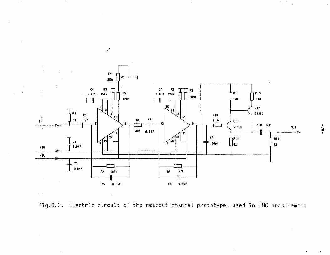
/
Ri
111311
Ci R3 e.tn 15111 R5
H 12n
B
Q :: 9
C3 9 19
IH lpF " :.. I s II
lei •611 J0.8i7
:.. -Gt.t
C2
I e.111 c:J-
R2 l08k
cs 8. 8pF
C7 R3 R~ 8.93J 2i01
H~ 1001
tG ll
17 RB C7
CJ-I 12 1a
206 1.017 2 01
21 3
--
R5 27k
I~-CB 6.E'<!F
All Rl3
101 180
VT2
Rl0 2!363
t .31< lJll
21368 cu
-I C9 RU IOOpF ll2
•
hF
RI I
51
- .
Cl. I _,
-00- "' I
Fig.3.2. Electric clrcuit of the readout channel prototype, used in ENC measurement

i
The value of ENC, calculated with formula 13.31, describes the full noise of the system. To get in consideration the noise of the measuring tract itself one have to perform the measurement of sigma_tract with the preamplifier turned off. The sigma_tract is being calculated with the same fitting procedure mentioned above.
Then the response amplitude standard deviation of the preampli-' fier itself is calculated:
~ 4/2 (3"preamp = I 6fu11·2 - vtract"2) 13.4)
Putting the calculated value of sigma_preamp into the formula 13.31 one obtains the ENC of the preamplifier itself.
The calculated value of the ENC together with some auxilary information !the charge-to-voltage conversion coefficient, the detector capacity, the shaping time etc. l is being wrote to the computer hard disk, where the information about tested lot of !C's is being accumulated.
When all measurement are finished, the program of format transformation makes file in the GRAPHER format for the visual interpretation of the measurement results.
3.2. The BJT version IC measurements results
Electric connection circuit of the BJT version channel 1 of CSP/Shapers IC to measure ENC is drown in Fig.3.2. An CSP input head transistor of the first channel is supposed theoretically to have Rbb' = 93 Ohm. A CSP output signal comes to a SS input with time characteristics determined by capacitances C7, CB and resistors RS, RB. The values to be used in the test circuit form Tp = 300 nsec. The filtered signal trough the buffer amplifier !transistors VT1 and VT2l comes to the sample oscilloscope 50 Ohm input.
Three external elements are connected to CSP and SS. The capacitances C4 and C7 shunt high frequency oscillations which may have arisen at the cascade and reference JFETs' gates. Resistors R3 and RB set drain currents of common gate stages. The drain curents may have values 100 - 200 uA. The cascade JFET drain current increasing causes the channel dissipated power to increse, and the curent decreasing cause the JFET transconductance to decrease and consequently to decrease the circuit gain and speed. Resistors R4, RS and R9 regulate the CSP/SS head transistor currents. The values of resistors shown in Fig.3.2. give the possibility to change this currents in interval 0.5 - 1.0 mA. The current lower boundary restriction is caused by the fact that the JFETs' gate voltage can't be more positive than +6 V. The upper boundary current restricion is due to transition of the cascade JFET to resistive operation region at larger values of the current. All the noise measurements have been made at the head transistor collector current equal 0.61 mA. This current value corresponds to minimum ENC for the most of CSP chips as exemplified by a drawing in Fig. 3.3.
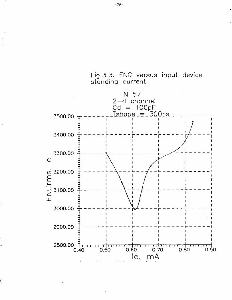
3500.00
3400.00
3300.00
u) 3200.00
E L
:__) 3100.00 7 ..LI
.3000.00
2900.00
-78-
Fig.3.3. ENC versus input device standing current
N 57 2-d channel Cd = 100pF
_______ lsbape_~_3000~---------1 I I I I I I I
I I I I -----,-----,-----,-----,-----! I I I ..- I
-----r-----r~---r-----1 J./ I
_____ L __ _
I
I -----r-----
--1------1------1 I
___ L _____ L ____ _
I I
I I ----r-----r-----, I I
I I I I -----r-----r-----r-----r-----1
I I I I I I I I
I I I
2800.00 0.40 0.50 0.60
le, 0.70
mA 0.80 0.90

In Figs. 3.4 - 3.6 are shown the output signals of the CSP, SS and FS. The slow shaper peaking time Tp = 300 nsec. In such conditions the dependence ENC = flCdJ was measured for both channels of five chips. The curves are presented in Figs. 3. 7, 3.8. It is seen that the channel 1 CSP with the head BJT Rbb' supposed to be equal 93 Ohm has ENC about 200 - 300 e- more, than this for the channel 2, whose input transistor Rbb' has supposed to be equal 15 Ohm. The slope of the curve ENC = f !Cdl is approximately the same for al I the chips and is equal to no more than 8 e-/pF for most of the chips !7elpF for the best one, see fig.3.91.
The CSP and SS open loop voltage gain estimated in the test is equal Kv = 800.
The power dissipated in one channel ICSP+SS+FSJ is measured to be equal Psup = 67 mW. This value is one third Jess again the specified one due to the Jess head transistor collector current optimised for ENC.
In Figs.3.10, 3.11 are presented ENC histograms of 51 and 57 chips for the first and the second channels respec~~i.vt.\1 11.t C.J~~OO pF to compare the noise characteristics of the two channels. The histogram area of the first channel input device is less than that of the second channel.
3.3. The JFET version IC measurements results
The electric circuit of the JFET version channel 1 connection for ENC measurements is presented in Fig. 3. 12. In this circuit the slow shaper is connected as an integrator, the fast one - as a differentiator. This configuration is explained by the unsuff icently low gain of the JFET version CSP which forced us to achieve an additional gain in the shaper stages. The peaking time Tp = 300 nsec, shaper's gain is 10. The buffer amplifier made of transistors VTl and VT2 transmits the signal to the 50 Ohm impedance sample oscilloscope.
In fig. 3.13 the first channel ENC dependence on a detector capacity is shown. The head JFET there has larger size and larger gate capacitance !about 10 pFJ and hence better capacitance matching. ENC for this case is substantially lager than for the BJT version and can be represented as ENC = 3300e + 20e/pF at the interval of Cd = 0 - 220 pF.
The second channel has the head CSP JFET of Jess size and gate capacitance !about 6 pFJ. Its noise is estimated to be equal ENC = 4400e + 27e/pF. The preamplifiers of all the two channels have open loop voltage gain not enough to be used as a charge-sensitive preamplifiers for CSC muon detectors: Ku = 57 for the first channel CSP and Ku = 30 for the second one.
The output signals of the preamplifier and the signal path shaper are shown in Fig. 3.14.

-80-
Fig.3.4. Preamplifier response, Channel 2, Vin=100 mV, Cin=lpF, Cd=100pF.

-81-
Fig. 3.5. Response of the circuit, presented on the Fig 3.2, Channel 2,
Vi=100mV, Cin=lpF, Cd=100pF.

-82-
Fig.3.6. Fast shaper response. Channel 2.
Vin=100mV, Cin=lpF,Cd=100pF.

4500.00
4000.00
Q) 3500.00
(f)
E L 3000.00
~ 7
..LI 2500.00
2000.00
-83-
Fig.3.7. ENC versus detector capacity (first channel)
NN 50,51,52,57,65 1 channel le = 0.61 mA Tshape = 300ns
-----------------------------1
I I I I
------~-------L--- --~-------1 I I
I I I
------~-------1
I I I
~-------L------~-------1 I I I I I I I I I I I I
------~-------L------~-------1 I I I I I I I I
1500.00 0.00 50.00 100.00 150.00 200.00
Cd, pF

<D
-CJ)
-64-
•
Fig .3.8. ENC ver·sus detector· capacity (second channel)
5000.00
4500.00
4000.00
3500.00
NN 50,51,5? ,54,5 7 2-d channel le = 0.61mA
______ _TsbDpe ___ 300o~---------' I I I I I I I I
------~-------~------~-------! I I I I
I I I I
----,-------,
I --------------'
E '-.L 3000.0Q :__) 7
.,.....,__,~- ~~ - - ~ - - - - - - -I - - - - - - -.LI 2500.00 :i----~-;::;fl" I I
2000.00
1500.00
1000.00 0.00
-----,-------r-------,-------1 I I I I I I I I ------,-------,------,-------! I I
I I
50.00 100.00 150.00 200.00
Cd, pF

3200.00
3000.00
2800.00
Q)
2600.00 -Ul
E I,_ 2400.00 :_) 7 JJ 2200.00
2000.00
1800.00
-85-
Fig.3.9
N 50 2-d channel le = 0.61mA Tshape = 300ns -----------------------------· I
I I ------~-------~------ _______ ,
I I I I I I I I I I I ------,-------r-- ---,-------1
------~------ I I ,------,-------! I
------~-- ----L------~-------1 I I I I
~-------~------~-------
' 198qe+7ej'pF ------,-------r------,-------
1 I I I I I I I I ------,-------,------,-------! I I I
1600.00 ~.-.-.-.--.-.--.-..-.-1-r..,....,....,....,...,.....,....,.....,...-1-r-T""T'"T""T""T""T""T"T""f-r-,r-ri-.--.-.-.-.-I
0.00 50.00 100.00 150.00 200.00
Cd, pF
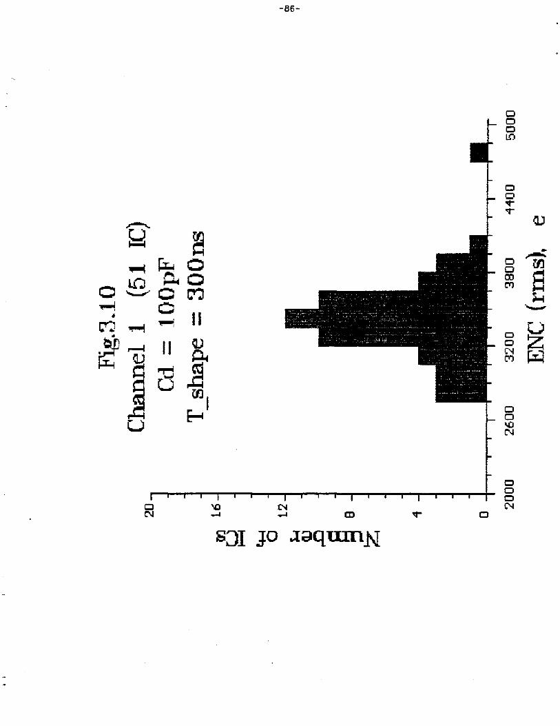
..-.... 61 ~ ~ r.. 0 ln ~ 0
0 - 0 C"'J ._, 0 • 11 C':J "'!"-! ~ •
~~ II QJ
] j 'IJ u oo, &-! u
'\O ......
-66-
SJI JO .i~qmnN 0
0 0 0 l!'.l
0 0
"'" '1""
0 0 co Cl')
0 0 N C"')
0 0
"' N
0 0 0 N
QJ
• --oo 8 ~ --~ ~
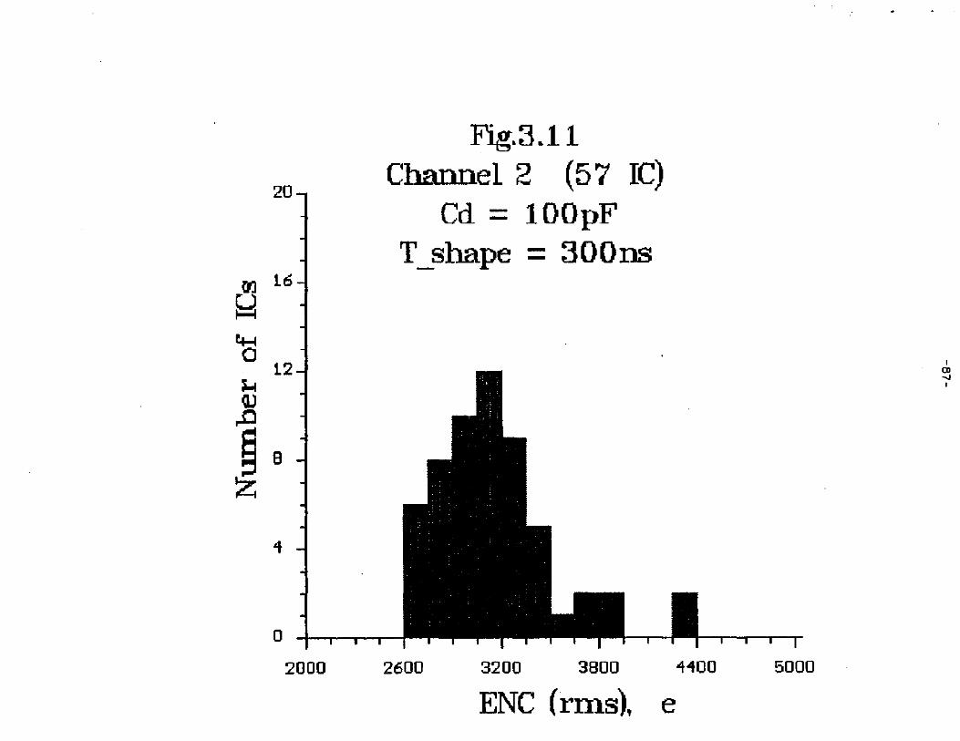
20
ff.) l6
~
~ ~ Q.)
..0
l2
§ a z
...
0
2000
Fig.3.11 Channel 2 (57 IC)
Cd= lOOpF T_shape = 300ns
2600 3200 3800
ENC (rms), e 4100 5000
I tu -.J I

(])
~
(j)
E !......
(_) z w
,-"
-88-
Fig.3.13. ENC versus detector capacity for the first channel of the JFET version of IC
Is = 1 OmA
14000.00 ____ I~~a_p_e ___ -~O_O_n~ ____________ .
I I I I
12000.00
10000.00
------:-------:------~~--______ J-------~---rr~~ -------:
I I V I
I I I I
8000.00 ------~-------~- ----~-------!
6000.00
I x I I I
___ ~ a~ [ 9 _____ ~ ______ J _______ : \\..7 I I I
I I I I I
4000.00 I I I I
-----~--~----r------~-------,
2000.00 ------~-------r------~-------1 I I I I
0. 00 -+-.--.-.--.-.,..,.-.,--,-,-r-,--,-,....,..,,..,....,--,-,-r-, ....... ,..,....,~.--.--.-+-r-r-r-r-r-r-r-r-rl
0.00 100.00 200.00 300.00 400.00
Cd, pF
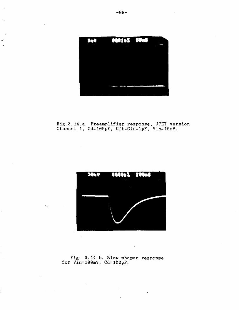
-89-
Fig.3. 14.a. Preamplifier response, JFET version Channel 1, Cd=100pF, Cfb=Cin=lpF, Vin=10mV.
Fig. 3.14.b. Slow shaper response for Vin=100mV, Cd=100pF.
-90-
The Pspice simulation with the mentioned above refined element parameters gives gain value 42 as it is seen from Figs. 1.16, 1.17. The low open loop voltage gain causes the the strong conversion factor dependence on a detector capacitance Cd to be evident from Figs. 1.14 and 1.15. Connection a capacitor 100 pF to the input of the CSP leads to one third degradation of the CSP output signal. The open loop voltage gain for the circuit chown in Fig. 1.13 may be calculated with the formula Ku= Gmax•R2. The voltage gain is supposed to be increased by introducing of an active load to the cascade stage. lt should be noted another drawback of this JFET version circuit. The circuit element parameter dispersion forced us to use an additional external resistor R !see Fig.3.111 to increse a drain current of VTl and to set operational point of the circuit. To eliminate this drawback we must change the circuitry of this JFET version.
3.4. The measurement results discussion
The next conclusions are supposed to be made based on the reported results of the first iteration CSC front-end IC measurements.
3.4.1. The first version of JC contained two channels, each being consisted of a charge-sensitive preamplifier with microwave bipolar transistor with Rbb' supposed to be equal 15 Ohms used as an input head transistor, followed by a slow shaper in signal path and a fast shaper in trigger path, have ENC less than 3000 r.m.s.e- at detector capacitance Cd = 100 pF and peaking time Tp = 300 nsec. The best samples have ENC = 1960e + 7e/pF, the tipical value of the slope is BelpF. The dissipated power is Jess than 70 mW per channel at the noise opnimum value of the head transistor collector current being equal 0.61 mA.
3.4.2. The same channel but with the head transistor possessing Rbb'= 93 Ohm have about 200 - 300 r.m.s.e- more ENC than the mentioned above measured at the same conditions. It seems possible to achieve an additional diminishing of ENC through the further lowering of Rbb', but it must have not be very large according our calculations reported in chapter l of this report and in literature [20 , 211.
3.4.3. The second IC version of the same configuration but with p-type JFET head transistor with gate capacitance Cg = 10 pF has ENC = 3300e + 20elpF at the same conditiones. The dissipated power is equal 150 mW per channel at the standard connecion, but it is possible to diminish this value to approximately 60 mW per channel by decreasing the negative suppling voltage. The CSP has open loop voltage gain Ku= 57. Tis value seems to be too small to use the circuit for CSC muon detector.
3.4.4. The channel with the head JFET of less size has noise ENC = 4400e + 27elpF <this value may have been refined in future in the direction of Jess noise values}. The dlssipated power is some less than in the former case. Voltage gain is too small again and is equal 30.
3.4.5. The BJT version JC is supposed to be refined in the next way:
3.4.5.1. The minimum size BJT with AREA= 0.012 used in the output CSP stage should be enlarged or replaced with a Darlington's emitter follower to increse the ouput power of the circuit and to improve its stability in respect to autoexcitation.
3.4.5.2. The resistor in the head transistor emitter circuit should be remaved to enlarge the input stage transconductance and open loap volt3ge gain.
3.4.5.3. The slowffast shaper circuit version is investigated which ·has JFET output stage.

-91-
3.4.6. The JFET head transistor version is considered to introduse the next improvements:
3.4.6.1. The head transistor transconductance should be enlarged to decrease the series input resistance to Rs = 20 Ohm.
3.4.6.2. The active load should be introduced to the cascade stage to enlarge the open loop voltage gain and through this to diminish the dependence of charge-to-voltage transformance coefficient on the input capacitance.
3.4.6.2. The electric circuit should be modified to exclude possible lathing due to monolithic circuit parameter scattering.
3.5.7. Pspice simulations results after the models refinements are in a good agreement with values measured on the real IC.
3.5.8. The measurement bench should be refined to give more versatility.

-92-
CONCLUSIONS
On the base of all the investigations reported above it is possible to make the next conclusions:
- the supposed combined BJT-JFET technology seems to be appreciable for GEM CSC front-end custom monolithic electronics;
- the refined electronic component models used in Pspice simulations proved to provide satisfactory coincidence of the parameters the simulated circuits and realized IC;
- the IC version with the head microwave BJT appears to be acceptable after future modernization for CSC muon detector; the first iteration product IC consisted of a charge-sensitie preamplifier followed by slow signal shaper and fast trigger one have demonstrated the noise performance ENC = 1980 + 7elpF at input capacity 100 pF, peaking time 300 nsec and dissipated power less than 70 mW per channel;
- the IC version with the head JFET needs in circuit modernization due to low open loop voltage gain; neerhteless, it seems to be promising too because good performance of JFET being used as a head element;
- the second design iteration should made further impact on problems of multiplication of cannel-per-chip number, diminishing of the interconnection capacitors values and dissipated power, stability in respect to autoexcitation;
- the slow shaper should realize RC-CR"4 filtering; - the measurement bench should be modified for mor versatility. Ue hope to take all this in account during the second design
iteration.

-93-
REFERENCES
1. Kostromin P. P. et al. Fast operating Proportional Chamber Working with Freon-14 and Jsobutane Mixture: !HEP preprint 67-59.-Serpukhov, 1967. -p6, figs. 4, refs.: 4
2. Kurchaninov L.L. et al. Fast-Cicling Minidrift Chamber with Freon-14 160%1 and Jsobutan 120%1 Mixture: !HEP Preprint 69-131.-Serpukhov, 1969.-p.6, figs. 4, refs.: 6
3. R.J. Yarema, T. Zimmerman. A High Speed, High Gain Preamplifier System for Silicon Strip Detectors: IEEE Trans. Nucl. Sci., Vol. 37, No. 2 April 1990
4. N.N. Fediakin et al. Cable connection between detector and preamp! ifier to avoid the radiatin damage: NucJ. Instr. and Meth., A317 119921, 313-314
5. V. Radeca, IEEE Trans. Nucl. Sci. Ns-21, No. 1 119741 p.51 6. A. Gola et al. Monolithic Readout electronics for the Silicon Calo
rimeters at SSC/LHC Colliders: Nucl. Phys. B !Proc. Suppl. l 23A 11991! 207-213
7. A. Gola et al. Monolithic matching of silicon detectors with high number of channels at very short shaping time: Nucl. Instr. and Meth. A320 119921 317-324
8. P. F. Manfredi, V. Sperzial i. High Densiti Mono! ithic Front-End Systems for Detectors without Charge Multiplication: NucJ. Instr. and Meth. A279 (19691 152-166
9. W. Butler et al. JFET-CMOS Microstrip Front-end. NucJ. Instr. and Meth. A279 (19691 204-211
10. E. Nygard et al. CMOS Low Noise Amplifier for Microstrip Readout. Design and Results. Nucl. Instr. and Meth. A301 ( 1991! 506-516
11. W. Butler. Short Channel, CMOS-compatible JFET in Low Noise Appl ications, Nucl. Instr. and Meth. A326 !19931 63-70
12. W. Butler et al. NJFET-PMOS preamplifier System: an upgraded version. Nucl. Instr. and Meth. A315 !1992! 420-424
:3. Eric Beuville et al. Amplex, a Low-Noise, Low-Power Analog CMOS Signal Processor for Multi-Element Silicon Particle Detectors. Nucl. Instr. and Meth. A288 ( 1990! 157-167
14. Nucl. Instr. and Meth. A253 (1987! 439-443 15. Nucl. Instr. and Mi>th. A300 !1991! 335-342 16. IEEE Trans. on Electr. Devices. 1986. - V.35, N11, 1924-1934 17. Proc. IEEE Custom Integrated Circuits Conference. -
1967. pp.341-344. 18. Electrical specifications for the GEM CSC Readout.
Version 1.0. Prinston-Brookhaven, May 25, 1992. 19. Summary of GEM CSC Discussion at Dubna, June 15-17, 1992 20. P.F.Manfredi et al. Low noise design of readout electronics for
microstrip vertex detectors. Nucl. Instr. and Meth. A274 !1969! 477-464
21. Veljko Radeka. Low-noise techniques in detectors. Ann. Rev. Nucl. Part. Sci. 1988, 36, 217-277

-94-
Al. APPENDIX. PSPICE SIMULATION PROTOCOL
Al.1. BJT version
••••••• 05112193 ••••••• PSpice 4.03A - March, 1990 ••••••• 13:35:58 •••••••
dvorn
**** CIRCUIT DESCRIPTION
****************************************************************************
.opt nopage nomod
~Fast shaper rl l 10 Zk ql 10 3 4 mods O.S r2 4 ~ 10 <.
j4 14 9 10 kpf 2 r7 14 2 7k q9 1 14 23 modS 0.5 rll 23 2 2.7k Rfbl 23 3 33k •Rshortl 1 9 0.001 Vgl 9 0 4
Cinl 61 3 lZpf
•Charge sensitive preamplifier r3 1 11 2k q2 11 5 6 mods 5 r4 6 O 10 jS 15 13 11 kpf 2 q6 15 19 16 mods o.s r9 16 2 lk j10 24 1 1 kpf 2 j11 2 15 24 kpf 2 rfb2 24 5 100k cfb2 24 5 3.9pf •Rshort2 22 13 0.001 Vg2 13 0 5.3
qc2 19 19 72 modS 0.5 Rc2 72 2 !Ok Rc_ext2 0 19 200k
Cin2 62 5 1.6pf vin2 62 0 pulse(O 0.125 10ns 1ns lns 2000ns 10000nsl
•Connecting conductors Rshort2_1 24 61 0.001 Rshort2_3 24 63 O. 001

•Biasing network <preamp! r13 1 26 24k j13 27 22 26 kpf 2 q14 27 27 28 mods o.s qlS 28 51 29 mods O.S r14 29 2 2.8k r 17 1 35 1 k q19 3S 27 37 modS O.S q21 37 S! 38 mods o.s r19 38 2 !.4k r2! 1 22 24k q23 22 43 37 mods o.s r23 1 43 SOk q2S 43 43 4S modS O.S q27 4S S! 46 modS O.S r24 46 2 2.8k
q29 Sl S! 49 modS O.S r27 49 2 !Ok Rext2 S! 0 !60k
•SI ow shaper rS 1 12 2k q3 12 7 8 mod5 0.5 r6 8 2 10 j7 17 20 12 kpf 2 q8 17 21 18 modS o.s r10182!k q12 1 17 2S mods 0.5 r12 2S 2 10k rfb3 25 7 100k •cfb3 2S 7 5.6pf •Rshort3 34 20 0.001 Vg3 20 0 S.3
qc3 21 21 82 mods 0.5 Rc3 82 2 !Ok Rc_ext3 0 21 SOOk
Cin3 63 7 1000pf
•Biasing network (slow r!S 1 30 24k }'is 31 34 30 kpf 2 q17 31 31 32 mod5 0.5 q18 32 52 33 mods 0.5 r16 33 2 2.Bk rlB 1 36 lk q20 36 31 39 modS 0.5 q22 39 S2 40 mod5 o.s r20 40 2 !.4k r22 1 34 24k q24 34 44 39 modS o.s r"r:: -~ 1 44 SOk q26 44 44 47 mod5 o.s q28 47 52 48 modS o.s r26 48 2 2.8k
forml
-ss-

q30 52 52 50 mod5 0.5 r28 50 2 10k Rext3 52 0 160k
v 1 1 0 6 v2 2 0 -6
-96-
.MODEL MODS NPN 15=95e-18 BF=92 VAF=S.34 IKF=23M ISE=95e-18 xtb=l.5 + NE=1.2 BR=0.7 VAR=S.34 IKR=lM ISC=2.39E-13 NC=2 RB=20.4 IRB=lOM + RBM=13.5 RE=4.0 RC=25.0 CJE=0.84P MJE=88m VJE=0.75 CJC=1.19P MJC=88m + VJC=0.82 XCJC=0.2 CJS=2.8P MJS=0.5 VJS=0.75 tr=lOn tf=11.8p itf=13.5m + vtf=!O xtf=2 .MODEL KPF PJF IVT0=-2.0 BETA=180U LAMBDA=SOM RS=21 RD=21 + CGS=2PF CGD=2PF FC=0.5 PB=! IS=1.7Fl .TRAN/OP 1n5 !OOOnS •.PRINT Vl25l .PROBE . end
INITIAL TRANSIENT SOLUTION TEMPERATURE = 27.000 DEG C
NODE VOLTAGE NODE VOLTAGE NODE VOLTAGE NODE VOLTAGE
1l 6.0000 2l -6.0000 3) -5.1946 4) -5.9864
5) .7267 6) .0081 7 l -5.2055 8) -5.9887
9l 4.0000 10) 2.7573 11) 4.0113 12) 3. 6379
131 5.3000 141 -4.0962 15) 1. 9837 16) -5.7988
17) -3.6543 !Bl -5.9444 191 -5.0653 20l 5.3000
21l -5.2294 22) 5.2417 231 -4.8460 24) 1. 8416
251 -4. 3779 261 3.7278 27) 1.3667 281 .6303
29) -5.7367 30) 3.7278 31) 1.3667 32) .6303
331 -5.7367 341 5. 2417 351 5.8596 36) 5.8596
37) .6364 38) -5.7537 39) .6364 401 -5.7537
43) 1. 3286 441 1. 3286 451 .5923 461 -5.7368
47) .5923 481 -5.7368 491 -5.7246 50) -5.7.246
51l -5.0207 52) -5.0207 611 1. 8416 62) 0.0000
63) 1. 8416 72> -5.7650 821 -5.9053

-97-
VOLTAGE SOURCE CURRENTS NAME CURRENT
Vgl -9.346E-12 Vg2 -4.612E-12 vin2 O.OOOE+OO Vg3 -1.062E-11 vl -6.827E-03 v2 6.119E-03
TOTAL POWER DISSIPATION 7.77E-02 WATTS •
**** OPERATING POINT INFORMATION TEMPERATURE = 27.000 DEG C
•••• BIPOLAR JUNCTION TRANSISTORS
NAME ql q9 q2 q6 qc2 MODEL mod5 mod5 mod5 mod5 mod5 IB 1. 06E-05 3.05E-06 1. 11E-OS 1. 83E-06 5.79E-07 IC 1. 35E-03 4.3SE-04 7.9SE-04 1.99E-04 2.29E-05 VBE 7.92E-01 7.SOE-01 7. 19E-01 7.33E-01 7.00E-01 VBC -7.9SE+OO -1. 01E+01 -3.28E+OO -7.0SE+OO 0.00E+OO VCE 8.74E+OO !. 08E+01 4.00E+OO 7.78E+OO 7.00E-01 BET ADC 1. 27E+02 1. 42E+02 7.13E+01 1. 09E+02 3.96E+01 GM 4.95E-02 1. 65E-02 3.04E-02 7. 62E-03 8.74E-04 RPI 2.61E+03 9.12E+03 2.S2E+03 1. S3E+04 4.88E+04 RX 4.07E+01 4.08E+Ol 4.0BE+OO 4.0BE+Ol 4.08E+Ol RO 9.24E+03 3.37E+04 9.94E+03 S.84E+04 2.02E+OS CBE 1. 09E-12 6.81E-13 S.18E-12 S.74E-13 4.91E-13 CBC 9.67E-14 9.48E-14 1. 03E-12 9.7SE-14 1.19E-13 CBX 3.87E-13 3.79E-13 4.13E-12 3.90E-13 4.76E-13 CJS 6.S4E-13 4.67E-13 S.S6E-12 7.3SE-13 6.13E-12 BETAAC 1. 29E+02 1. S1E+02 7.66E+Ol 1. 17E+02 4.26E+Ol FT S.01E+09 2.28E+09 4.67E+08 1. 14E+09 !. 28E+08
NAME q14 qlS q19 q21 q23 MODEL mod5 mods mods mods mods IB 2.09E-06 1. 01E-06 1. 66E-06 1.81E-06 4.43E-07 IC 9.09E-OS 9.30E-OS 1. 40E-04 1. 74E-04 3.16E-OS VBE 7.36E-01 7.16E-01 7.30E-01 7.33E-01 6.92E-Ol VBC O.OOE+OO -S.6SE+OO -4.49E+OO -S.66E+OO -3.91E+OO VCE 7.36E-01 6.37E+OO S.22E+OO 6.39E+OO 4.61E+OO BET ADC 4.3SE+01 9.19E+Ol 8.47E+Ol 9.61E+Ol 7. 13E+01 GM 3.44E-03 3.SSE-03 S.36E-03 6.64E-03 1. 21E-03

-98-RP I 1. 34E+04 2.78E+04 1. 69E+04 1. S4E+04 6.39E+04 RX 4.08E+Ol 4.08E+Ol 4.08E+Ol 4.08E+01 4.08E+Ol RO S.06E+04 1. lOE+OS 6.48E+04 S.89E+04 2.71E+OS CBE S.2SE-13 S.24E-13 S.47E-13 S.62E-13 4.94E-13 CBC 1. 19E-13 9.92E-14 1.0lE-13 9.92E-14 1.02E-13 CBX 4.76E-13 3.97E-13 4.04E-13 3.97E-13 4.08E-13 CJS 8.34E-13 1.03E-12 4. 72E-13 1.03E-12 4.95E-13 BETAAC 4.61E+Ol 9.90E+Ol 9.04E+Ol 1. 03E+02 7.74E+Ol FT 4.89E+08 5.S6E+08 8. 11E+08 9.99E+08 1.92E+08
NAME q25 q27 q29 q3 q8 MODEL mods mods mod5 mod5 modS IB 2.09E-06 1. OlE·-06 6.71E-07 8.28E-06 9.86E-07 JC 9.09E-05 9.30E-05 2.69E-05 1. 13E-03 5.46E-05 VBE 7.36E-01 7.16E-01 7.04E-01 7.83E-01 7. lSE-01 VBC O.OOE+OO cS.61E+OO O.OOE+OO -8.84E+OO -1. SBE+OO VCE 7.36E-01 6.33E+OO 7.04E-01 9.63E+OO 2.29E+OO BET ADC 4.3SE+Ol 9.16E+Ol 4.0lE+Ol 1. 36E+02 S.S4E+Ol GM 3.44E-03 3.56E-03 1. 02E-03 4. lBE-02 2.09E-03 RP I 1. 34E+04 2. 77E+04 4.21E+04 3.34E+03 2.85E+04 RX 4.0BE+Ol 4.0BE+Ol 4.0SE+Ol 4.07E+01 4.0BE+Ol RO S.06E+04 1. 10E+05 1. 73E+05 1. 19E+04 1. 14E+05 CBE 5.25E-13 5.24E-13 4.93E-13 9.89E-13 5.07E-13 CBC 1.19E-13 9.93E-14 1.19E-13 9.58E-14 1. 08E-13 CBX 4.76E-13 3.97E-13 4.76E-13 3.83E-13 4.33E-13 CJS 8.42E-13 1. OSE-12 6.09E-12 S.83E-13 4.BlE-12 BETAAC 4.61E+Ol 9.86E+Ol 4.31E+Ol 1. 39E+02 S.94E+Ol FT 4.89E+08 5.5SE+08 1. SOE+08 4.53E+09 3. 17E+OB
NAME q12 qc3 q17 q18 q20 MODEL mods mods mod5 mod5 mod5 IB 1. 30E-06 2.SlE-07 2.09E-06 1. OlE-06 1.66E-06 IC 1. 69E-04 9.22E-06 9.09E-05 9.30E-05 1. 40E-04 VBE 7.24E-01 6.76E-01 7.36E-01 7. 16E-01 7.30E-01 VBC -9.65E+OO O.OOE+OO O.OOE+OO -S.65E+OO -4.49E+OO VCE 1. 04E+01 6.76E-01 7.36E-01 6.37E+OO 5.22E+OO BET ADC 1. 30E+02 3.68E+Ol 4.35E+Ol 9. 19E+Ol 8.47E+Ol GM 6.48E-03· 3.52E-04 3.44E-03 3.56E-03 5.36E-03 RP I 2. 16E+04 1. 13E+05 1. 34E+04 2.78E+04 1. 69E+04 RX 4.08E+Ol 4.08E+01 4.08E+01 4.0BE+Ol 4.0BE+Ol RO 8.43E+04 5.06E+OS 5.06E+04 1. lOE+OS 6.48E+04 CBE 5.S9E-13 4.82E-13 5.2SE-13 5.24E-13 5.47E-13 CBC 9.SlE-14 1.19E-13 1. 19E-13 9.92E-14 1.0lE-13 CBX 3.BOE-13 4.76E-13 4.76E-13 3.97E-13 4.04E-13 CJS 4.67E-13 6.28E-12 8.34E-13 1. 03E-12 4.72E-13 BETAAC 1. 40E+02 4.00E+Ol 4.61E+Ol 9.90E+Ol 9.04E+Ol FT 9.97E+08 5.21E+07 4.89E+08 S.56E+08 8.11E+08
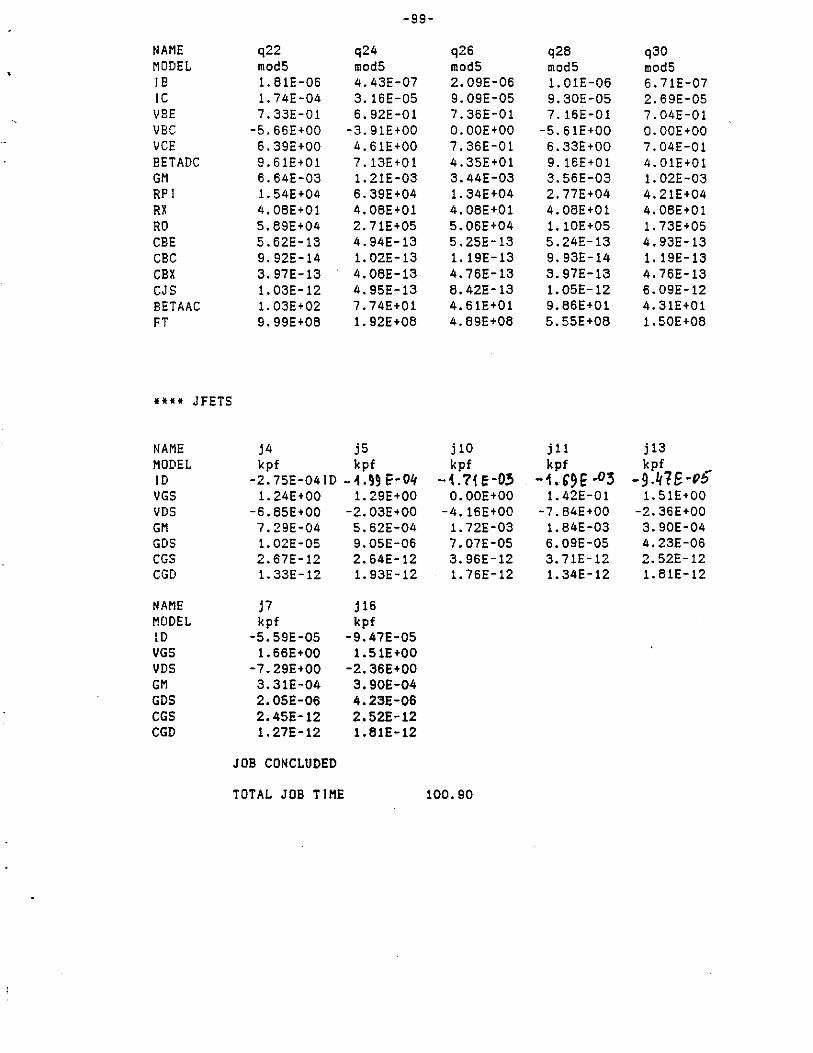
-99-
NAME q22 q24 q26 q28 q30 MODEL mods mods • modS modS mods IB 1. BlE-06 4.43E-07 2.09E-06 1. OlE-06 6.71E-07 IC 1. 74E-04 3.16E-OS 9.09E-OS 9.30E-OS 2. 69E-OS VBE 7.33E-01 6.92E-01 7.36E-01 7.16E-01 7.04E-01 VBC -5.66E+OO -3.91E+OO O.OOE+OO -S.61E+OO O.OOE+OO VCE 6.39E+OO 4.61E+OO 7.36E-01 6.33E+OO 7.04E-01 BET ADC 9.61E+01 7.13E+01 4.3SE+01 9. 16E+01 4.0lE+Ol GM 6.64E-03 1. 21E-03 3.44E-03 3.56E-03 1. 02E-03 RPI 1. S4E+04 6.39E+04 1. 34E+04 2.77E+04 4.21E+04 RX 4.0BE+Ol 4.0BE+Ol 4.08E+01 4.0BE+Ol 4.0BE+Ol RO S.89E+04 2.71E+05 S.06E+04 1. lOE+OS 1. 73E+05 CBE S.62E-13 4.94E-l3 S.2SE-13 S.24E-13 4.93E-13 CBC 9.92E-14 1. 02E-13 1. 19E-13 9.93E-14 1.19E-13 CBX 3.97E-13 4.0BE-13 4.76E-13 3.97E-13 4.76E-13 CJS 1. 03E-12 4.95E-13 8.42E-13 1. OSE-12 6.09E-12 BETAAC 1. 03E+02 7.74E+01 4.61E+01 9.86E+01 4.31E+01 FT 9.99E+OB 1.92E+08 4.89E+08 S.SSE+OB 1. SOE+OB
**** JFETS
NAME j4 jS jlO j 11 j13 MODEL kpf kpf kpf kpf kpf ID -2. 7SE-041D -~.99 E'-01/ --t. 7i e-03 - 'I • '9 E -0 :5 -9.41B-P5 VGS 1. 24E+OO 1. 29E+OO O.OOE+OO 1. 42E-01 1. 51E+OO VOS -6.BSE+OO -2.03E+OO -4.16E+OO -7.84E+OO -2.36E+OO GM 7.29E-04 S.62E-04 1. 72E-03 1. 84E-03 3.90E-04 GOS 1. 02E-05 9.0SE-06 7.07E-05 6.09E-05 4.23E-06 CGS 2.67E-12 2.64E-12 3.96E-12 3.71E-12 2.52E-12 CGD 1. 33E-12 1. 93E-12 1. 76E-12 1.34E-12 1.BlE-12
NAME j7 j16 MODEL kpf kpf ID -5.59E-05 -9.47E-05 VGS 1.66E+OO 1.51E+OO VOS -7.29E+OO -2.36E+OO GM 3.31E-04 3.90E-04 GOS 2.0SE-06 4.23E-06 CGS 2.45E-12 2.S2E-12 CGD 1. 27E-12 1. BlE-12
JOB CONCLUDED
TOTAL JOB TIME 100.90
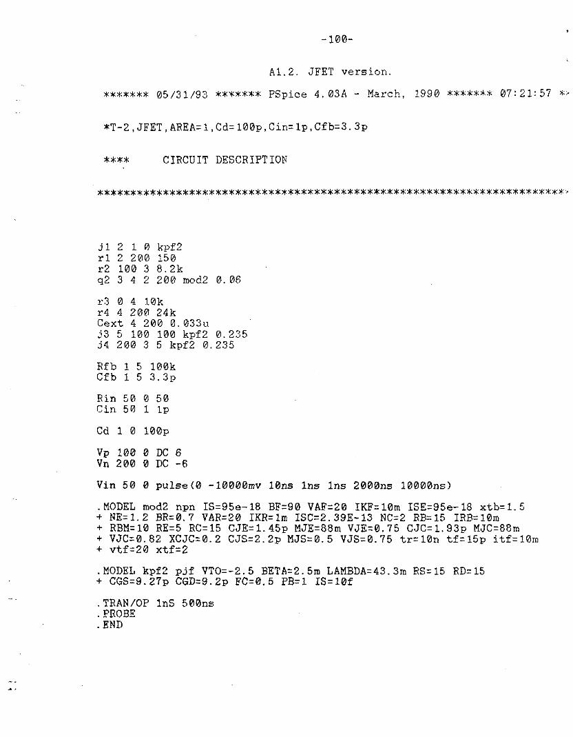
-100-
Al.2. JFET version.
******* 05 /31 /93 ******* PSpice 4. 03A - March, 1990 ******* 07: 21: 57 *'
*T-2,JFET,AREA=l,Cd=l00p,Cin=lp,Cfb=3.3p
**** CIRCUIT DESCRIPTION
***********************************************************************'
j 1 2 1 0 kpf2 rl 2 2Ql0 150 r2 100 3 8. 2k q2 3 4 2 200 mod2 0. 06
r3 0 4 10k r4 4 200 24k Cext 4 200 0.033u j3 5 100 100 kpf2 0.235 j4 200 3 5 kpf2 0.235
Rf b 1 5 100k Cfb 1 5 3. 3p
Rin 50 0 50 Cin 50 1 lp
Cd 1 0 100p
Vp 100 0 DC 6 Vn 200 0 DC -6
Vin 50 0 pulse(0 -10000mv 10ns lns lns 2000ns 10000ns)
.MODEL rnod2 npn IS=95e-18 BF=90 VAF=20 IKF=10rn ISE=95e-18 xtb=l.5 + NE=l.2 BR=0.7 VAR=20 IKR=lm ISC=2.39E-13 NC=2 RB=15 IRB=10rn + RBM=10 RE=5 RC=15 CJE=l.45p MJE=88rn VJE=0.75 CJC=l.93p MJC=BBm + VJC=0.82 XCJC=0.2 CJS=2.2p MJS=0.5 VJS=0.75 tr=10n tf=15p itf=10m + vtf=20 xtf=2
.MODEL kpf2 pjf VT0=-2.5 BETA=2.5m LAMBDA=43.3m RS=15 RD=l5 + CGS=9.27p CGD=9.2p FC=0.5 PB=l IS=10f
.TRAN/OP lnS 500ns
. PROBE
.END
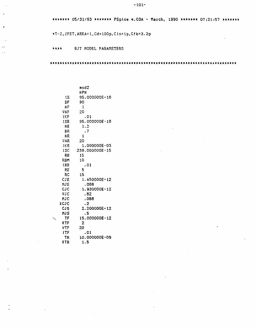
-101-
••••••• 05131193 ******* PSpice 4.03A - March, 1990 ******* 07:21:57 •••••••
•T-2,JFET,AREA=l,Cd=l00p,Cin=lp,Cfb=3.3p
**** BJT MODEL PARAMETERS
****************************************************************************
mod2 NPN
IS 95.000000E-18 BF 90 NF 1
VAF 20 !KF .01 !SE 95. OOOOOOE - 18
NE l.2 BR • 7 NR 1
VAR 20 !KR 1. OOOOOOE-03 ISC 239.000000E-15
RB 15 RBM 10 !RB .01
RE 5 RC 15
CJE 1. 450000E-12 MJE .088 CJC 1. 930000E-12 VJC .82 MJC .088
XCJC .2 CJS 2.200000E-12 MJS • 5
" TF 15.000000E-12 XTF 2 VTF 20 ITF .01 TR 10.000000E-09
XTB 1.5

-102-
******* 05131/93 ******* PSpice 4.03A - March, 1990 ******* 07:21:57 *******
•T-2,JFET,AREA=1,Cd=100p,Cin=1p,Cfb=3.3p
**** Junction FET MODEL PARAMETERS
****************************************************************************
VTO BETA
LAMBDA RD RS
CGD CGS
kpf2 PJF -2. 5 2.500000E-03
. 0433 15 15 9.200000E-12 9.270000E-12
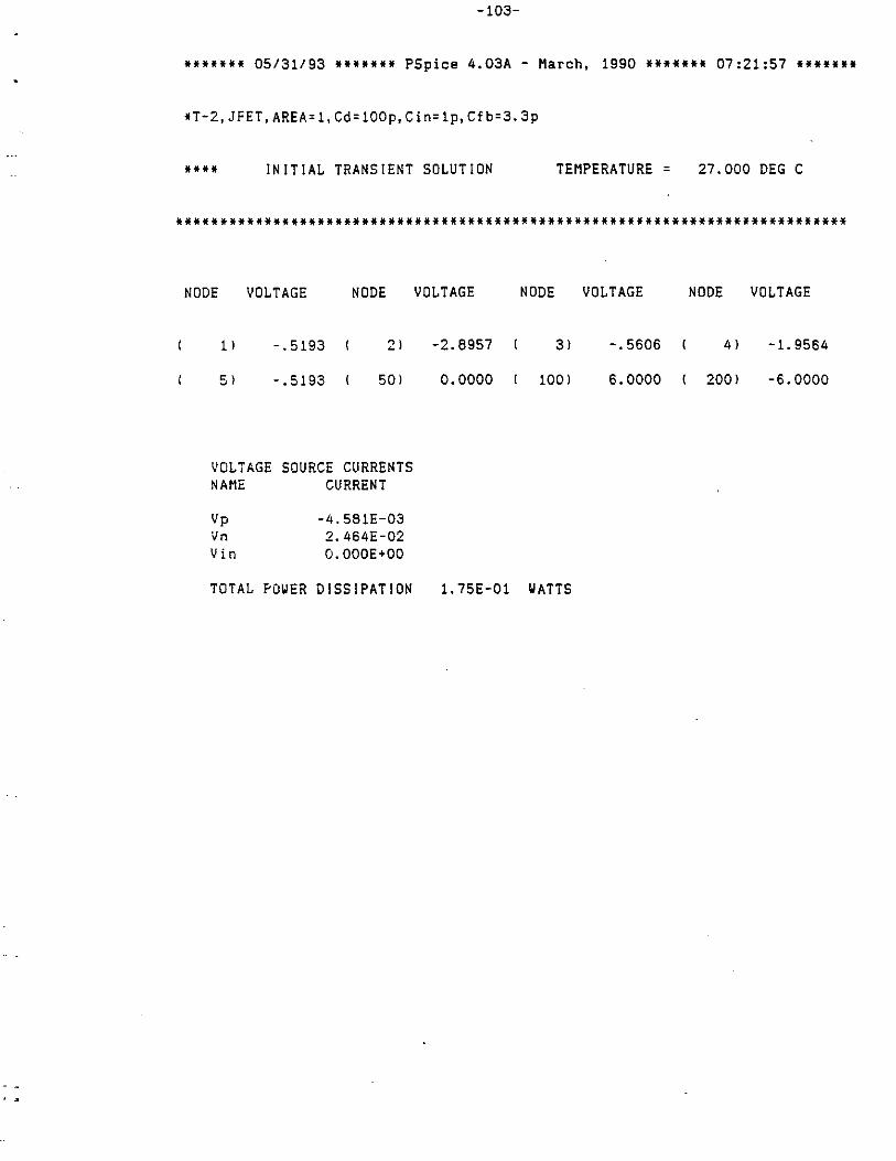
. .
-103-
******* 05/31193 ******* PSpice 4.03A - March, 1990 ******* 07:21:57 *******
•T-2,JFET,AREA=1,Cd=100p,Cin=lp,Cfb=3.3p
**** INITIAL TRANSIENT SOLUTION TEMPERATURE = 27.000 DEG C
****************************************************************************
NODE VOLTAGE NODE VOLTAGE
1l -.5193 21 -2.8957
5) -.5193 501 0.0000
VOLTAGE SOURCE CURRENTS NAME CURRENT
Vp Vn Vin
-4.581E-03 2.464E-02 O.OOOE+OO
NODE VOLTAGE
3) - . 5606
100) 6.0000
TOTAL ~OWER DISSIPATION 1. 75E-O 1 WATTS
NODE VOLTAGE
4) -1.9564
200) -6.0000
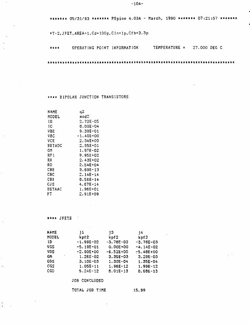
-104-
******* 05/31/93 ******* ?Spice 4.03A - March, 1990 ******* 07:21:57 *******
•T-2,JFET,AREA=1,Cd=100p,Cin=1p,Cfb=3.3p
**** OPERATING POINT INFORMATION TEMPERATURE = 27.000 DEG C
*************************************'**************************************
•••• BIPOLAR JUNCTION TRANSISTORS
NAME MODEL IB IC VBE \'BC VCE BET ADC GM RPI RX RO CBE CBC CBX CJS BETAAC FT
**** JFEiS
NAME MODEL ID VGS VDS GM GOS CGS CGD
q2 mod2 2.?ZE-05 8.00E-04 9.39E-01
-1. 40E+OO 2.34E+OO 2.95E+01 1. 97E-02 9.95E+02 2.43E+02 2.54E•04 9.69E-13 2.14E-14 8.56E-14 4.67E-14 1.96E+01 2.91E+09
jl kpf2
-1.99E-02 -5.19E-01 -2.SOE+OO
1. 26E-02 3.lOE-03 1. 05E-11 5.24E-12
JOB CONCLUDED
TOTAL JOB TIME
j3 kpf2
-3.78E-03 O.OOE+OO
-6.52E+OO 3.35E-03 1. 30E-04 1. 96E-12 B. OlE-13
j4 kpf2
-3.7BE-03 -4.14E-02 ~5.4BE+OO
3.29E-03 1. 35E-04 1. 99E-12 B.SBE-13
15. 99