edc lab pec-351 semester: iii - dbit.ac.in · manual practical instruction sheet experiment no. 1...
TRANSCRIPT
AIM:- FIELD EFFECT TRANSISTORS: - Single stage common source FET amplifier-plot of
gain in db Vs frequency, measurement of, bandwidth, input impedance, maximum signal
handling capacity (MSHC) of an amplifier.
EQUIPMENT REQUIRED:-
S no. Particulars Specification/Range Quantity Make/Model No.
1. Trainer kit 1 2. Connecting
wires
3. multimeter 1
4. CRO 1
CRO, Signal generator, Power Supply, Bread-board, Resistors (1MΩ, 4.7KΩ, 1KΩ), Capacitors
(10μF, 100Μf), FET-BFW10 and connecting Wires.
THEORY:-
A JFET can be N-channel type or P-channel type. The structure of a P-channel JFET is similar to
that of an N-channel JFET. Except that in its structure, N-type is replaced by P-type and P-type by
N-type. The structure of an N-channel JFET is abar of N-type silicon. This bar behaves like a
resistor between its two terminals, called source and drain. We introduce heavily doped P-type
region on either side of bar. These P-regions are called gates. Usually two gates are connected
together. This gate is used to control current flow from source to drain. This flow of electrons makes
the drain current Id. The electrons in the bar pass through the space between the two P-regions. As
width of this space between the p-regions can be controlled by varying gate voltage that is called a
channel. We apply a small reverse bias to the gate. Because of the reverse bias, the width of
depletion increases. Since the N-type bar is lightly doped compared to the P-regions, the depletions
region extends more into the N-type bar. This reduced the width of the channel. Reduction in the
width of the channel (the conductive portion of the bar) increases its resistance. This reduces the
Dev Bhoomi Institute Of Technology
Department of Electronics and Communication
Engineering
LABORATORY
MANUAL
PRACTICAL INSTRUCTION SHEET
EXPERIMENT NO. 1 ISSUE NO. : ISSUE DATE: July 2010
REV. NO. : REV. DATE :
PAGE: 5
LABORATORY Name & Code: EDC LAB PEC-351 SEMESTER: III
drain current Id. There is one important point about the channel shape. It is narrower at the drain end.
This happens because the amount of reveres bias is not same throughout the length of the P-N
junction. When current flows through the bar, a potential drop occurs across its length. As a result
the reverse bias between the gate and the drain end of the bar is more than that between the gate and
the source end of the bar. The width of depletion region is more at the drain end than at the source
end. As a result, the channel becomes narrower at the drain end. If the reverse gate bias is increased
further, the channel becomes narrower at the drain end and drain current further reduces. If the
reverse bias is made sufficiently large, the depletion region will extend into channel. This pinches
off all current flow. The gate-source voltage at which pinch-off occurs is called PINCH-OFF voltage
Vp.
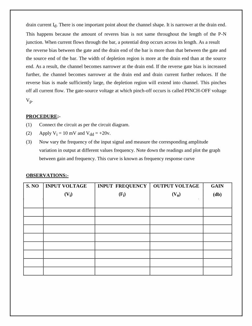
PROCEDURE:-
(1) Connect the circuit as per the circuit diagram.
(2) Apply Vi = 10 mV and Vdd = +20v.
(3) Now vary the frequency of the input signal and measure the corresponding amplitude
variation in output at different values frequency. Note down the readings and plot the graph
between gain and frequency. This curve is known as frequency response curve
OBSERVATIONS:-
S. NO INPUT VOLTAGE INPUT FREQUENCY OUTPUT VOLTAGE GAIN
(Vi) (Fi) (Vo) (db)

RESULT:-
Thus we have plotted a graph between gain and frequency to obtain a frequency response curve. The
values of fL and fH from graph are given as
FH =
FL =
BW = FH - FL
PRECAUTIONS:-
(1) All connections should be right and tight. (2) Readings should be taken carefully. (3) Scale on the graph should be taken correctly and carefully.
PRE EXPERIMENTAL QUESTIONS:
Q. Define FET.
A. The field-effect transistor (FET) is a transistor that uses an electric field to control the shape and
hence the conductivity of a channel of one type of charge carrier in a semiconductor material. FETs
are sometimes called unipolar transistors to contrast their single-carrier-type operation with the
dual-carrier-type operation of bipolar (junction) transistors (BJT). The concept of the FET predates
the BJT, though it was not physically implemented until after BJTs due to the limitations of
semiconductor materials and the relative ease of manufacturing BJTs compared to FETs at the time.
Q. What are different terminals of FET?
A. The FET's three terminals are: Source (S), through which the majority carriers enter the channel. Conventional current entering the
channel at S is designated by IS.
Drain (D), through which the majority carriers leave the channel. Conventional current entering the
channel at D is designated by ID. Drain to Source voltage is VDS.
Gate (G), the terminal that modulates the channel conductivity. By applying voltage to G, one can
control ID

POST EXPERIMENTAL QUESTIONS:
Q. What are advantages of the FET.
A. The main advantage of the FET is its high input resistance, on the order of 100M ohms or more.
Thus, it is a voltage-controlled device, and shows a high degree of isolation between input and
output. It is a unipolar device, depending only upon majority current flow. It is less noisy and is thus
found in FM tuners for quiet reception. It is relatively immune to radiation. It exhibits no offset
voltage at zero drain current and hence makes an excellent signal chopper. It typically has better
thermal stability than a BJT.
Q. What are disadvantages of the FET?
A. It has relatively low gain-bandwidth product compared to a BJT. The MOSFET has a drawback of being very susceptible to overload voltages, thus requiring special handling during installation.
Q. What are the various applications of FET?
A. Applications are in switching internal combustion engine ignition coils, where fast switching and voltage blocking capabilities are important. The most commonly used FET is the MOSFET. The CMOS (complementary metal oxide
semiconductor) process technology is the basis for modern digital integrated circuits. This process technology uses an arrangement where the (usually "enhancement-mode") p-channel MOSFET
and n-channel MOSFET are connected in series such that when one is on, the other is off.

Single Stage RC Coupled FET Amplifier
Frequency Response
AIM :- Bipolar transistor:- Designing of single stage RC coupled amplifier-design of DC biasing
circuit using potential divider arrangement – plot of frequency Vs gain in db. Measurement
of bandwidth of an amplifier, input impedance and Maximum signal Handing Capacity of
an amplifier.
APPARATUS:-
S no. Particulars Specification/Range Quantity Make/Model No.
1. Trainer kit 1
2. Connecting
wires
3. multimeter 1
4. CRO 1
CRO, Power supply, Signal Generator, Bread-board, Resistors, capacitors ,transistor (BC 107) and
connecting wires.
Design of RC coupled amplifier (DC biasing circuit design)
Design values: design a voltage divider circuit for given values:
IC = 2mA VCE = 4V
RC = 2KΩ VCC = 10V
Determine the values of R1, R2,and RE.
Solution:
Ic =β IB IB = Ic
β
I1 = 10 X IB
I1 = VCC
R1+R2
VCE = VC-VE
VCE = VCC-ICRC-IERE …………(IC=IE)
Dev Bhoomi Institute Of Technology
Department of Electronics and Communication
Engineering
LABORATORY
MANUAL
PRACTICAL INSTRUCTION SHEET
EXPERIMENT NO. 2 ISSUE NO. : ISSUE DATE: July 2010
REV. NO. : REV. DATE :
PAGE: 6
LABORATORY Name & Code: EDC LAB PEC-351 SEMESTER: III
VCE = VCC-IC (RC+RE)
Ic = VB-VBE RE
VB=IC X RE
VB= R2 X VCC
R1+R2
THEORY: Almost no electronic system can work without an amplifier. The voice of a single person
could reach everybody in a hall only because of the amplification of the signal picked up by the P.A
system. After a transistor is biased in the active region, it can work as an amplifier. We apply an ac
voltage between the base and emitter terminals to produce fluctuations in the collector current .An
amplified output signal is obtained when this fluctuating collector current flows through a collector
resistor Rc.When the input signal is so weak as to produce small fluctuations in the collector current
compared to its quiescent value, the amplifier is called ‘small signal amplifier’ (also ‘voltage
amplifier’). Such an amplifier is used as the first stage of the amplifier used in receivers (radio and
TV), tape recorders, and stereos and measuring instruments.The circuit of a single stage transistor
amplifier is shown in fig. Almost all amplifiers use potential divider biasing circuit because the design
of the circuit is simple and it provides good stabilization of the operating point. If this circuit is to
amplify ac voltages, some more components must be added such as the circuit capacitors are added.
The capacitor CC is called coupling capacitors. A coupling capacitor passes an ac signal from one side
to another. The capacitor CE works as a bypass capacitor. It bypasses all the ac currents from the
emitter to ground. The resistance R represents the resistance of whatever is connected at the output.
To what extent an amplifier enlarges signal is expressed in terms of its voltage gain. The voltage gain
of an amplifier is given as –
AV = output AC voltage / input AC voltage
AV = Vo/Vi
The other quantities of interest for a voltage amplifier are current gain (Ai) input impedance (zi ) and
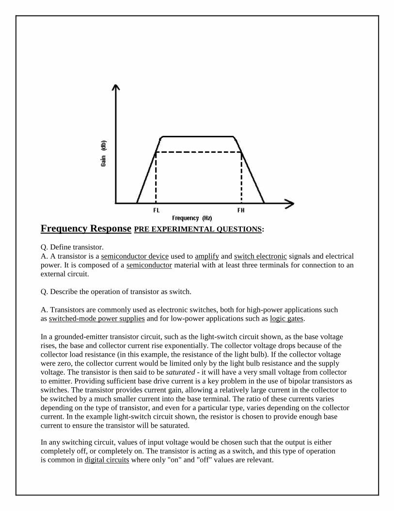
output impedance (zo).The performance of an amplifier is judged by observing whether all frequency
component of the signal are amplified equally well. The information is provided by its frequency response
curve. This curve illustrates how the magnitude of voltage gain of the amplifier varies with the freq. of the
input signal (sinusoidal). It can be plotted by measuring voltage gain of the amplifier
for different frequencies of sinusoidal voltage fed to its input. Fig shows the frequency response
curve of the typical RC coupled amplifier.
B.W = f2 – f1
PROCEDURE:-
(1) Connect the circuit as the cat. Diagram.
(2) Apply Vcc = +15V &set i/p voltage in mV.
(3) Now vary the frequency of i/p voltage &Measure the corresponding amplitude variation in
o/p at different values of i/p frequency.
(4) Not down the reading and plot a graph between gain and frequency. The curve is known as
frequency response curve.
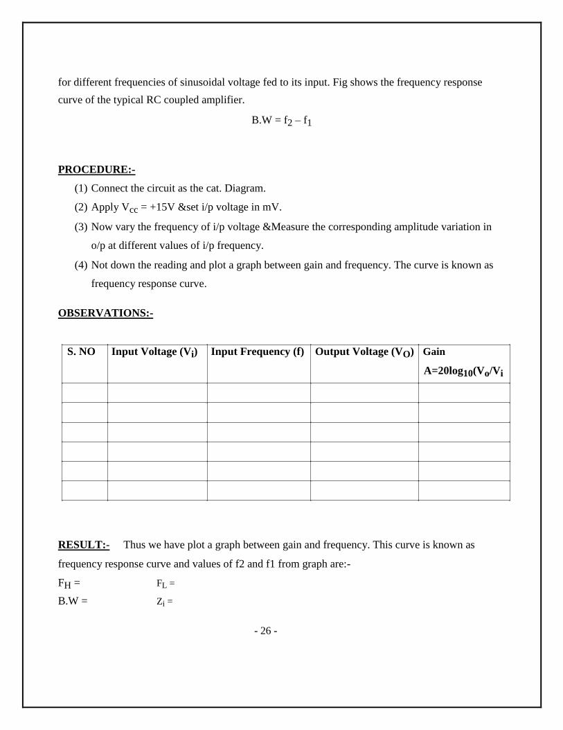
OBSERVATIONS:-
S. NO Input Voltage (Vi) Input Frequency (f) Output Voltage (VO) Gain
A=20log10(Vo/Vi
RESULT:- Thus we have plot a graph between gain and frequency. This curve is known as
frequency response curve and values of f2 and f1 from graph are:-
FH = FL =
B.W = Zi =
- 26 -
Max signal handling capacity =
PRECAUTIONS:-
(1) All connection should be right & tight.
(2) Readings should be taken carefully.
(3) Scale on the graph should be taken correctly & carefully.
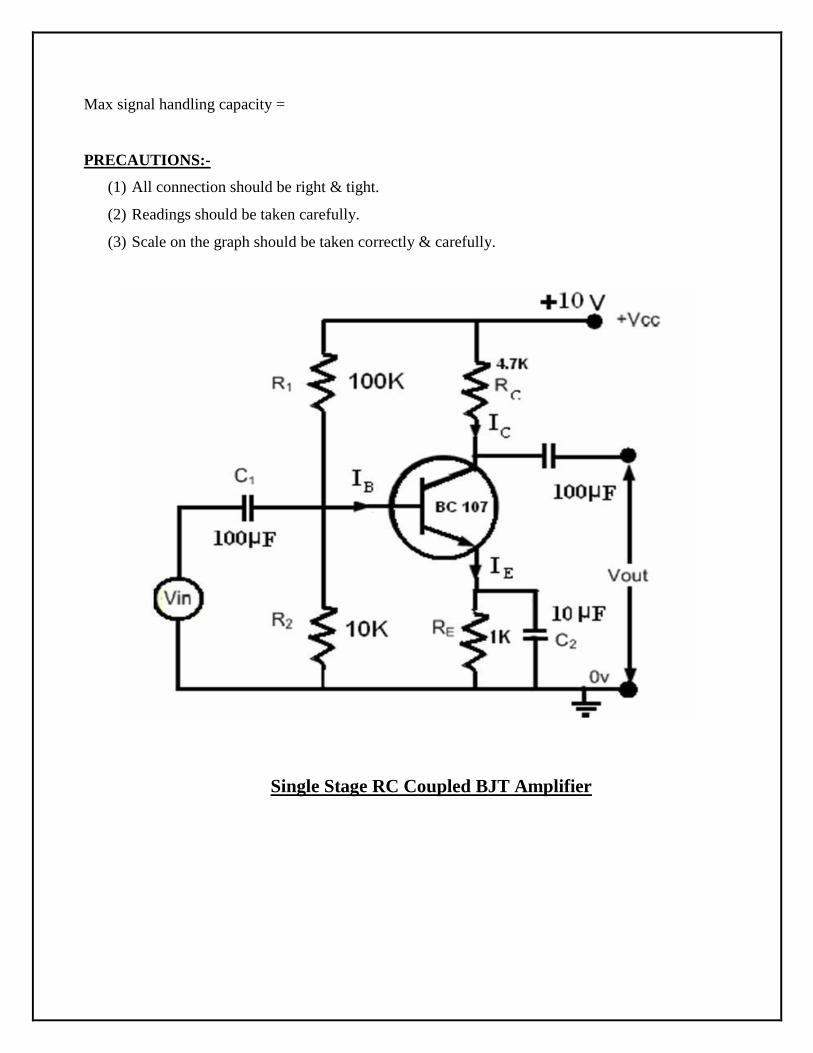
Single Stage RC Coupled BJT Amplifier
Frequency Response PRE EXPERIMENTAL QUESTIONS:
Q. Define transistor. A. A transistor is a semiconductor device used to amplify and switch electronic signals and electrical
power. It is composed of a semiconductor material with at least three terminals for connection to an
external circuit.
Q. Describe the operation of transistor as switch.
A. Transistors are commonly used as electronic switches, both for high-power applications such as switched-mode power supplies and for low-power applications such as logic gates.
In a grounded-emitter transistor circuit, such as the light-switch circuit shown, as the base voltage
rises, the base and collector current rise exponentially. The collector voltage drops because of the
collector load resistance (in this example, the resistance of the light bulb). If the collector voltage
were zero, the collector current would be limited only by the light bulb resistance and the supply
voltage. The transistor is then said to be saturated - it will have a very small voltage from collector
to emitter. Providing sufficient base drive current is a key problem in the use of bipolar transistors as
switches. The transistor provides current gain, allowing a relatively large current in the collector to
be switched by a much smaller current into the base terminal. The ratio of these currents varies
depending on the type of transistor, and even for a particular type, varies depending on the collector
current. In the example light-switch circuit shown, the resistor is chosen to provide enough base
current to ensure the transistor will be saturated.
In any switching circuit, values of input voltage would be chosen such that the output is either
completely off, or completely on. The transistor is acting as a switch, and this type of operation is common in digital circuits where only "on" and "off" values are relevant.

POST EXPERIMENTALQUESTIONS:
Q. Name the ternimals of the transistor.
A. Emitter, Collector and Base.
Q. Why BJT Call as bipolar device?
A. Bipolar transistors are so named because their operation involves both electrons and holes, as
opposed to unipolar transistors, such as field-effect transistors, in which only one carrier type is
involved in charge flow. Although a small part of the transistor current is due to the flow of
majority carriers, most of the transistor current is due to the flow of minority carriers and so BJTs
are classified as minority-carrier devices.
Q. Why BJT called as current controlled device?
A. The collector–emitter current can be viewed as being controlled by the base–emitter current
(current control), or by the base–emitter voltage (voltage control). These views are related by
the current–voltage relation of the base–emitter junction, which is just the usual exponential
current voltage curve of a PN junction (diode)
The physical explanation for collector current is the amount of minority-carrier charge in the base
region. Detailed models of transistor action, such as the Gummel–Poon model, account for the
distribution of this charge explicitly to explain transistor behavior more exactly. The charge-control
view easily handles photo-transistors, where minority carriers in the base region are created by the
absorption of photons, and handles the dynamics of turn-off, or recovery time, which depends on
charge in the base region recombining. However, since base charge is not a signal that is visible at the
terminals, the current- and voltage-control views are usually used in circuit design and analysis.
EXPERIMENT NO – 5
AIM:- Two Stage Amplifiers: - Plot of frequency Vs gain, Estimation of Q factor, bandwidth of an
amplifier.
APPARATUS:-
S no. Particulars Specification/Range Quantity Make/Model No.
1. Trainer kit 1
2. Connecting
wires
3. multimeter 1
4. CRO 1
C.R.O Power supply, Signal Generator, Bread – board , Resistors ,Capacitors , transistors &
Connecting wires.
THEORY:- Gain of a single transistor amplifier Stage is not sufficient & has two or more stages are
usually connected in cascade to provide the desired gains me times cascading is done to achieve the
correct I/P or O/P impedance for a specific application. Most Popular cascade amplifier is formed by
cascading several CS amplifier Overall gain A = A1. A2 Where A1 & A2 are the gain of individual
stages.
PROCEDURE:-
(1) Connect the circuit as per the ckt. Diagram.
(2) Apply VDD =20v & set I/p voltage in mv.
(3) Now vary the frequency of I/p & measure the corresponding amplitude variation in o/p at
different values of I/p frequency.
(4) Note down the reading and plot a graph between gain and frequency. The curve is known as
frequency response curve.
Dev Bhoomi Institute Of Technology
Department of Electronics and Communication
Engineering
LABORATORY
MANUAL
PRACTICAL INSTRUCTION SHEET
EXPERIMENT NO. 3 ISSUE NO. : ISSUE DATE: July 2010
REV. NO. : REV. DATE :
PAGE: 6
LABORATORY Name & Code: EDC LAB PEC-351 SEMESTER: III
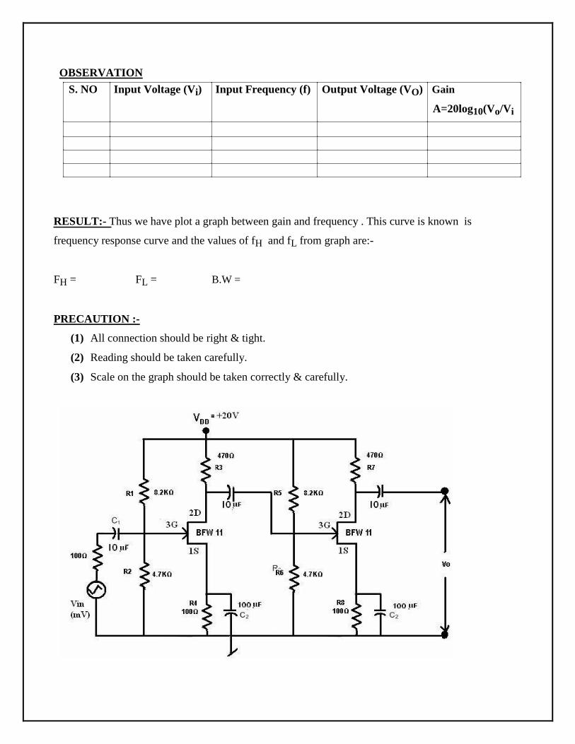
OBSERVATION
S. NO Input Voltage (Vi) Input Frequency (f) Output Voltage (VO) Gain
A=20log10(Vo/Vi
RESULT:- Thus we have plot a graph between gain and frequency . This curve is known is
frequency response curve and the values of fH and fL from graph are:-
FH = FL = B.W =
PRECAUTION :-
(1) All connection should be right & tight.
(2) Reading should be taken carefully.
(3) Scale on the graph should be taken correctly & carefully.
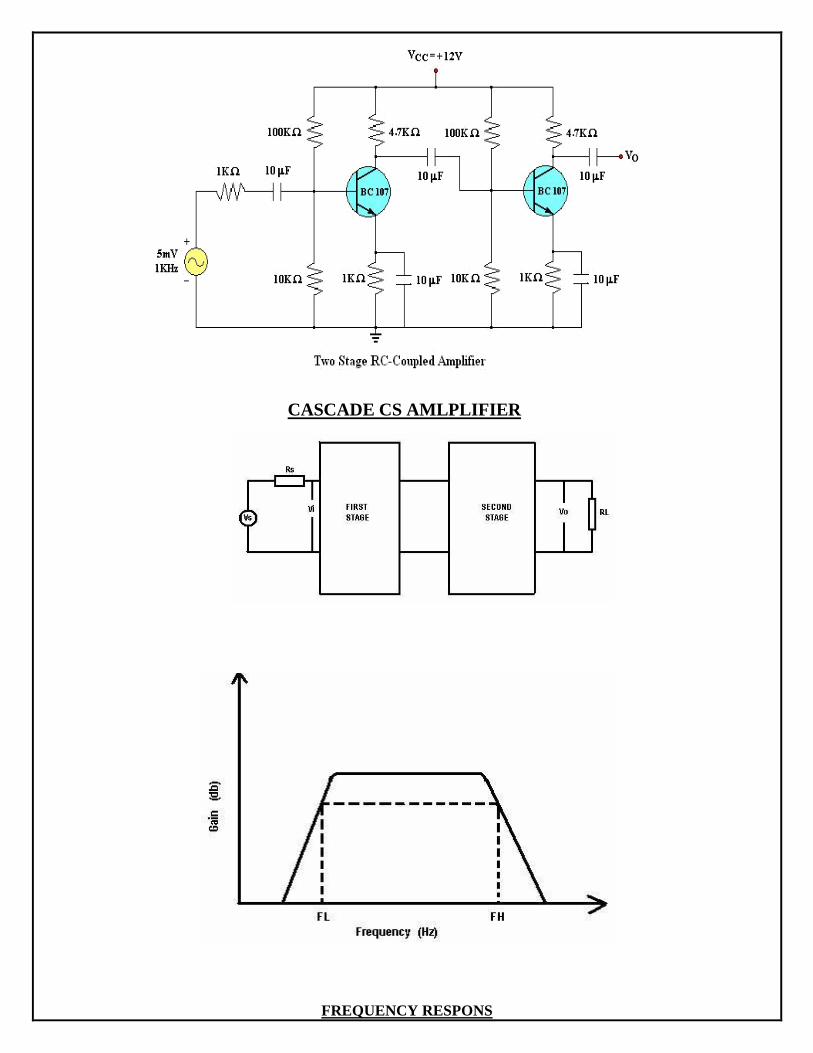
CASCADE CS AMLPLIFIER
FREQUENCY RESPONS

EXPERTMENT NO -6
AIM:- Common Collector configuration-Emitter follower (using Darlington Pair):-Gain and
input impedance measurement of the circuit.
APPARATUS REQUIRED:
S no. Particulars Specification/Range Quantity Make/Model No.
1. Trainer kit 1 2. Connecting
wires
3. multimeter 1
4. CRO 1
NV6542 trainer, Digital Multimeter (DMM), Multimeter probes, 2mm Patch chords, Mains cord.
Theory:
Emitter Follower (using Darlington Pair)
In recent years, electronics have been integrated into motor speed drives and a variety of
Switching-type power supplies. This means that standard discrete components needed to be
altered to provide better characteristics.The need for the Darlington pair grew from the limitations
of SCRs and triac-type thyristors. Thyristors control current by delaying the turn-on time. The
later the pulse is applied to turn them on, the smaller the amount of current they will conduct
during each cycle.On the other hand, a transistor uses variable current (0 to saturation), which
provides an output current that will be a duplication of the input. This means the transistors will
produce an analog signal when an analog signal is provided to its base. The simple bipolar
transistor has several limitations including slow switching speeds, low gains, and larger power
losses due to the switching process. A family of high-gain transistors called metal-oxide
Dev Bhoomi Institute Of Technology
Department of Electronics and Communication
Engineering
LABORATORY
MANUAL
PRACTICAL INSTRUCTION SHEET
EXPERIMENT NO. 4 ISSUE NO. : ISSUE DATE: July 2010
REV. NO. : REV. DATE :
PAGE: 6
LABORATORY Name & Code: EDC LAB PEC-351 SEMESTER: III
semiconductor field effect transistors (MOSFETs) was produced to address the gain problem, but
they did not have the capability of controlling larger currents, so the Darlington pair was
designed.The Darlington pair can actually be two discrete transistors that are connected in the
driver/output configuration, or they can be a single device that has the two transistors internally
connected at the point where it was manufactured as a single package. In Darlington pairs,
transistor collectors are tied together and the emitter of the first transistor is directly coupled to
the base of the second transistor. The total gain, which is often 1000 or more, is the- product of
the gain of the individual transistors. For large currents it is standard and good procedure to use a
Darlington pair of transistors, rather than a single one, which effectively acts like a single
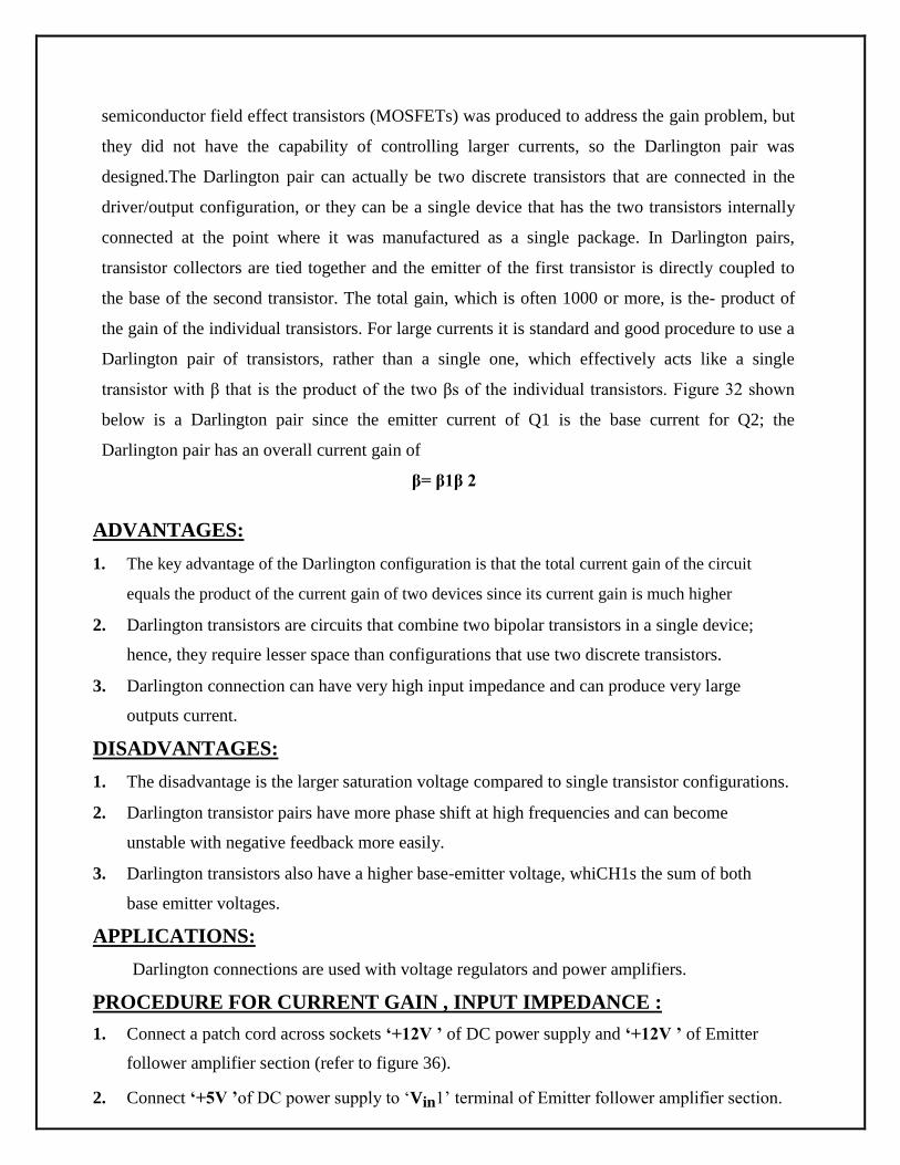
transistor with β that is the product of the two βs of the individual transistors. Figure 32 shown
below is a Darlington pair since the emitter current of Q1 is the base current for Q2; the
Darlington pair has an overall current gain of
β= β1β 2
ADVANTAGES:
1. The key advantage of the Darlington configuration is that the total current gain of the circuit
equals the product of the current gain of two devices since its current gain is much higher 2. Darlington transistors are circuits that combine two bipolar transistors in a single device;
hence, they require lesser space than configurations that use two discrete transistors. 3. Darlington connection can have very high input impedance and can produce very large
outputs current.
DISADVANTAGES:
1. The disadvantage is the larger saturation voltage compared to single transistor configurations. 2. Darlington transistor pairs have more phase shift at high frequencies and can become
unstable with negative feedback more easily. 3. Darlington transistors also have a higher base-emitter voltage, whiCH1s the sum of both
base emitter voltages.
APPLICATIONS:
Darlington connections are used with voltage regulators and power amplifiers.
PROCEDURE FOR CURRENT GAIN , INPUT IMPEDANCE :
1. Connect a patch cord across sockets ‘+12V ’ of DC power supply and ‘+12V ’ of Emitter
follower amplifier section (refer to figure 36).
2. Connect ‘+5V ’of DC power supply to ‘Vin1’ terminal of Emitter follower amplifier section.
3. Connect a patch cord between socket A and B of Emitter follower amplifier section. 4. Connect a patch cord between socket E and F. 5. Now set the digital multimeter’s dial to DC voltage mode. 6. Now connect the multimeter through multimeter probes to ‘A’ and ‘G1’.
7. Switch on the power supply. 8. Now measure the DC voltage between ‘A’ and ground ‘G1’ using DMM. This will give value
of dc voltage input Vin to the transistor T1.Note it down. 9. Switch off the power supply. 10. Calculate the input current (Ii) by substituting the value in following equation
Iin = (Vin1-Vin)/ Rs
Where, Vin1 =5 V,Rs =100 KΩ,Vin =DC voltage measured in step 8.
11. Note down this value of input current Iin. 12. Calculate the input impedance (Zin) by following formula in step 10.
Zin =Vin/ Ii
13. Now remove the patch cord between sockets ‘+5V’ and ‘Vin1’ 14. Also remove the patch cord between sockets ‘A’ and ‘B’. Connect a patch cord between socket
E and F.
15. Now connect ‘+5V’ directly at the base terminal ‘B’ of transistor T1. 16. Remove the patch cord between socket ‘E’ and ‘F’ and connect a DMM through probes
between the sockets ‘E’ and ‘F’
17. Now set the digital multimeter’s dial to DC current mode to measure the output DC Current,
Iout between the sockets ‘E’ and ‘F’ refer to figure). 18. Switch on the power supply.
19. Note down the value of output current Iout displayed on the DMM’s display. 20. Ratio of output current to input current gives the overall of Darlington pair.
Calculate the ratio of output current to input current by following formula
β= Iout / Ii
21. Individual of transistors can be calculated by considering the transistors having
identical and using the formula
β= β1x β2
β1=β2=’β
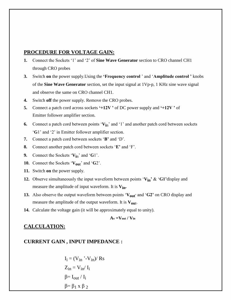
PROCEDURE FOR VOLTAGE GAIN:
1. Connect the Sockets ‘1’ and ‘2’ of Sine Wave Generator section to CRO channel CH1
through CRO probes 3. Switch on the power supply.Using the ‘Frequency control ’ and ‘Amplitude control ’ knobs
of the Sine Wave Generator section, set the input signal at 1Vp-p, 1 KHz sine wave signal
and observe the same on CRO channel CH1.
4. Switch off the power supply. Remove the CRO probes. 5. Connect a patch cord across sockets ‘+12V ’ of DC power supply and ‘+12V ’ of
Emitter follower amplifier section.
6. Connect a patch cord between points ‘Vin’ and ‘1’ and another patch cord between sockets
‘G1’ and ‘2’ in Emitter follower amplifier section. 7. Connect a patch cord between sockets ‘B’ and ‘D’. 8. Connect another patch cord between sockets ‘E’ and ‘F’.
9. Connect the Sockets ‘Vin’ and ‘G1’.
10. Connect the Sockets ‘Vout’ and ‘G2’. 11. Switch on the power supply.
12. Observe simultaneously the input waveform between points ‘Vin’ & ‘G1’display and
measure the amplitude of input waveform. It is Vin.
13. Also observe the output waveform between points ‘Vout’ and ‘G2’ on CRO display and
measure the amplitude of the output waveform. It is Vout. 14. Calculate the voltage gain (it will be approximately equal to unity).
Av =Vout / Vin
CALCULATION:
CURRENT GAIN , INPUT IMPEDANCE :
Ii = (Vin ’-Vin)/ Rs
Zin = Vin/ Ii
β= Iout / Ii
β= β1 x β 2
VOLTAGE GAIN:
Voltage Gain, Av = Vout / Vin
Where, Vin = Input Voltage, Vout = Output Voltage
RESULT:
Current Gain of Darlington Pair, β =………
Individual β of transistor = β’=.........
Input impedance of emitter follower =………Ω
Voltage gain of Darlington pair =………..V
Input Current
Input Voltage, Vin = 4.40 V
Iin = [Vin1 - Vin] / Rs
Iin = [5 - 4.40] / 100 x 10 3
Iin = 6 μ A
Input Impedance
Zin = Vin/ Ii
Zin = 4.40 / 6 x 10 -6
Zin = 733 K
Output Current
Iout = 35.4 mA
Current Gain of Darlington Pair
β= Iout / Iin
β= 35.4 mA / 6 μA
β= 5900
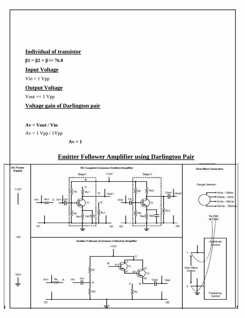
Individual of transistor
β1 = β2 = β√= 76.8
Input Voltage
Vin = 1 Vpp
Output Voltage
Vout == 1 Vpp
Voltage gain of Darlington pair
Av = Vout / Vin
Av = 1 Vpp / 1Vpp
Av = 1
Emitter Follower Amplifier using Darlington Pair
AIM:- Oscillators:- Sinusoidal Oscillator – (a) Wein bridge Oscillator
(b) Phase shift Oscillator
APPARATUS:-
S no. Particulars Specification/Range Quantity Make/Model No.
1. Trainer kit 1
2. Connecting
wires
3. multimeter 1
4. CRO 1
CRO ,Power supply , Bread– Board , IC 741, Resistor (3.3kΩ-2, 10kΩ),
Capacitors (0.05Μf-2).
THEORY:- The Wein-bridge Oscillator is a standard circuit for generating low frequency in the
rang of 10 HZ to 1MHZ . It is used all commercial audio generator. Wein-bridge is a ac bridge
which balances only at particular frequency called null frequency. When the bridge is balanced the
output of bridge is zero. For Oscillations to be sustained the phase shift to through the coupling
network must be zero. It can be shown that this condition occurs at a frequency given by
FO = 1/2IIRC
Here op-amp is used in non-inverting configuration and provides Oo phase shift. Since input
impedance is large and out put impedance is small for the OP-AMP, there is no loading on the feed
back network. When the above condition is satisfied we must have
β= 1/3
This means that amplifier must have a gain of at lest 3.
The Phase Shift oscillator produces positive feed back by using an inverting amplifier and adding
another 1800of phase shift with the three high pass filter circuit. It produces this 180
ophase shift for
only one frequency
Dev Bhoomi Institute Of Technology
Department of Electronics and Communication
Engineering
LABORATORY
MANUAL
PRACTICAL INSTRUCTION SHEET
EXPERIMENT NO. 5 ISSUE NO. : ISSUE DATE: July 2010
REV. NO. : REV. DATE :
PAGE: 4
LABORATORY Name & Code: EDC LAB PEC-351 SEMESTER: III
β= 1/29
This means that amplifier must have a gain of at lest 29
PROCEDURE:-
(1) Connect the circuit as per the diagram. on the bread-
board .
(2) Provide +/-12V Supply to the circuit.
(3) Observe the output sine wave on the CRO.
(4) Note the time period of this wave and calculate its
frequency. Also calculate the gain.
OBSERVATION:-
1. Calculate value of frequency of w.b. ocs. using the formula Wein-bridge
Fo = 1
2πRC
2.Calculate value of frequency of w.b. ocs. using the formula Wein-bridge
Fo = 1111
2II RC √6
3 . Practical Value of frequency as observed on CRO.
RESULT:- 1. Thus we have measured the frequency and gain for sine wave generated by Wein-
bridge oscillator.
PRECAUTION:-
1. All connections should be right and tight.
2. Readings should be taken carefully.
3. Power supply should be switched off after use.
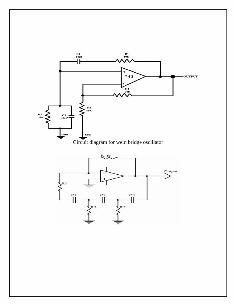
Circuit diagram for wein bridge oscillator
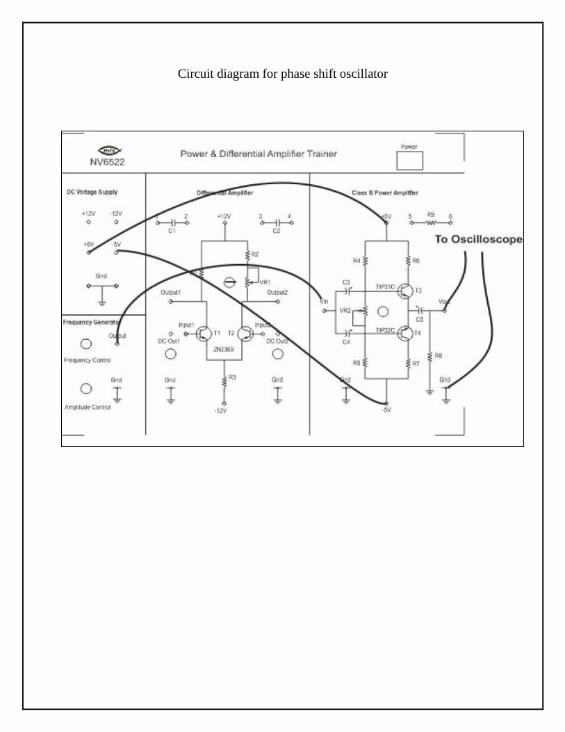
Circuit diagram for phase shift oscillator

COLPITTS OSCILLATOR
AIM: To determine the frequency of oscillations of a given Colpitts Oscillator.
APPARATUS:
S.No Name Range / Value Quantity
1. DC Regulated Power Supply (0-30V) 1
2. Resistors 560 , 47 K Each 1
4. Resistors 4.7 K 2
5. Capacitors 100 F, 0.047 F Each 1
6. Decade Inductance Box -- 1
7. Decade Capacitance Box -- 2
8. CRO -- 1
PROCEDURE:
1. Connect the circuit diagram as shown in the figure. 2. Switch on the power supply. 3. Connect the out put terminals to CRO. 4. Adjust the capacitances until a sinusoidal wave form is observed on the
CRO. 5. Measure the time period of the sinusoidal wave form (T) and determine the
Frequency (1/T).
6. Repeat the above steps for different values of L, C1 & C2. 7. Tabulate the readings and compare with theoretical values
CALCULATIONS:
f0 (practical) =1/T Hz.
1
C1C2
f0 (theoretical) f0 . [Where Ceq ]
2 LC
eq C1 C2
RESULT:
Dev Bhoomi Institute Of Technology
Department of Electronics and Communication
Engineering
LABORATORY
MANUAL
PRACTICAL INSTRUCTION SHEET
EXPERIMENT NO. 6(a) ISSUE NO. : ISSUE DATE: July 2010
REV. NO. : REV. DATE :
PAGE: 2
LABORATORY Name & Code: EDC LAB PEC-351 SEMESTER: III
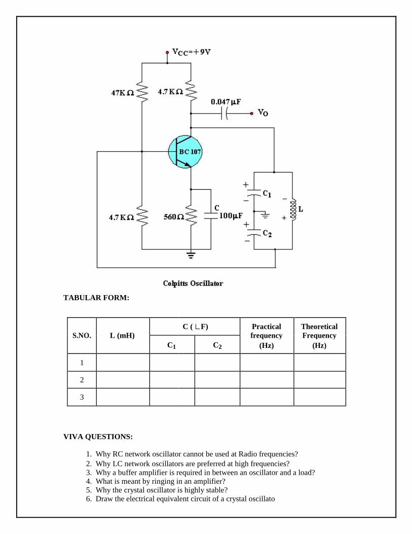
TABULAR FORM:
C ( F) Practical Theoretical
S.NO. L (mH)
frequency Frequency
C1
C2 (Hz) (Hz)
1
2
3
VIVA QUESTIONS:
1. Why RC network oscillator cannot be used at Radio frequencies? 2. Why LC network oscillators are preferred at high frequencies? 3. Why a buffer amplifier is required in between an oscillator and a load? 4. What is meant by ringing in an amplifier? 5. Why the crystal oscillator is highly stable? 6. Draw the electrical equivalent circuit of a crystal oscillato
RC-PHASE SHIFT OSCILLATOR
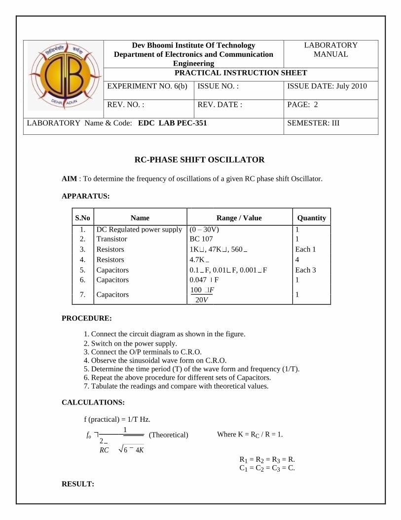
AIM : To determine the frequency of oscillations of a given RC phase shift Oscillator.
APPARATUS:
S.No Name Range / Value Quantity
1. DC Regulated power supply (0 – 30V) 1
2. Transistor BC 107 1
3. Resistors 1K , 47K , 560 Each 1
4. Resistors 4.7K 4
5. Capacitors 0.1 F, 0.01 F, 0.001 F Each 3
6. Capacitors 0.047 F 1
7. Capacitors
100 F 1
20V
PROCEDURE:
1. Connect the circuit diagram as shown in the figure. 2. Switch on the power supply. 3. Connect the O/P terminals to C.R.O. 4. Observe the sinusoidal wave form on C.R.O. 5. Determine the time period (T) of the wave form and frequency (1/T). 6. Repeat the above procedure for different sets of Capacitors. 7. Tabulate the readings and compare with theoretical values.
CALCULATIONS:
f (practical) = 1/T Hz.
fo 1
(Theoretical) Where K = RC / R = 1.
2
RC
6 4K R1 = R2 = R3 = R. C1 = C2 = C3 = C.
RESULT:
Dev Bhoomi Institute Of Technology
Department of Electronics and Communication
Engineering
LABORATORY
MANUAL
PRACTICAL INSTRUCTION SHEET
EXPERIMENT NO. 6(b) ISSUE NO. : ISSUE DATE: July 2010
REV. NO. : REV. DATE :
PAGE: 2
LABORATORY Name & Code: EDC LAB PEC-351 SEMESTER: III
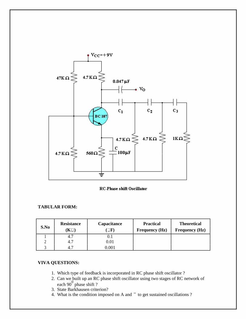
TABULAR FORM:
S.No Resistance Capacitance Practical Theoretical
(K ) ( F) Frequency (Hz) Frequency (Hz)
1 4.7 0.1
2 4.7 0.01
3 4.7 0.001
VIVA QUESTIONS:
1. Which type of feedback is incorporated in RC phase shift oscillator ? 2. Can we built up an RC phase shift oscillator using two stages of RC network of
each 900 phase shift ?
3. State Barkhausen criterion? 4. What is the condition imposed on A and to get sustained oscillations ?
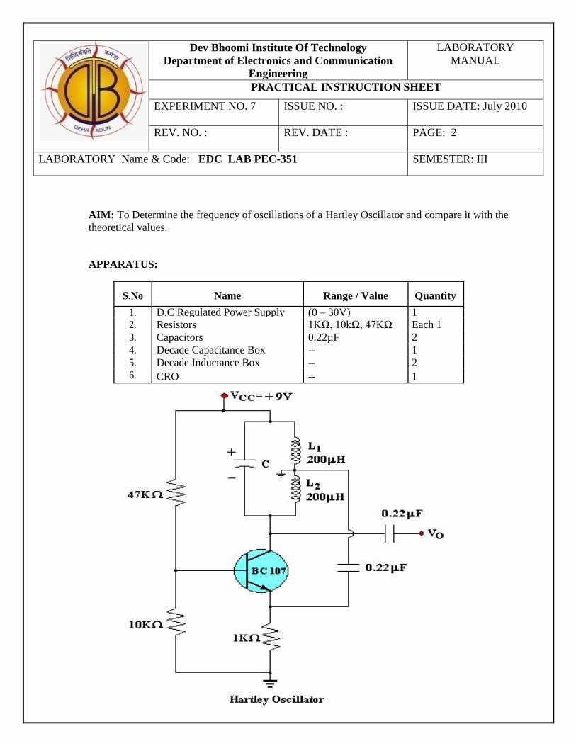
AIM: To Determine the frequency of oscillations of a Hartley Oscillator and compare it with the
theoretical values.
APPARATUS:
S.No Name Range / Value Quantity
1. D.C Regulated Power Supply (0 – 30V) 1 2. Resistors 1KΩ, 10kΩ, 47KΩ Each 1
3. Capacitors 0.22µF 2
4. Decade Capacitance Box -- 1
5. Decade Inductance Box -- 2
6. CRO -- 1
Dev Bhoomi Institute Of Technology
Department of Electronics and Communication
Engineering
LABORATORY
MANUAL
PRACTICAL INSTRUCTION SHEET
EXPERIMENT NO. 7 ISSUE NO. : ISSUE DATE: July 2010
REV. NO. : REV. DATE :
PAGE: 2
LABORATORY Name & Code: EDC LAB PEC-351 SEMESTER: III
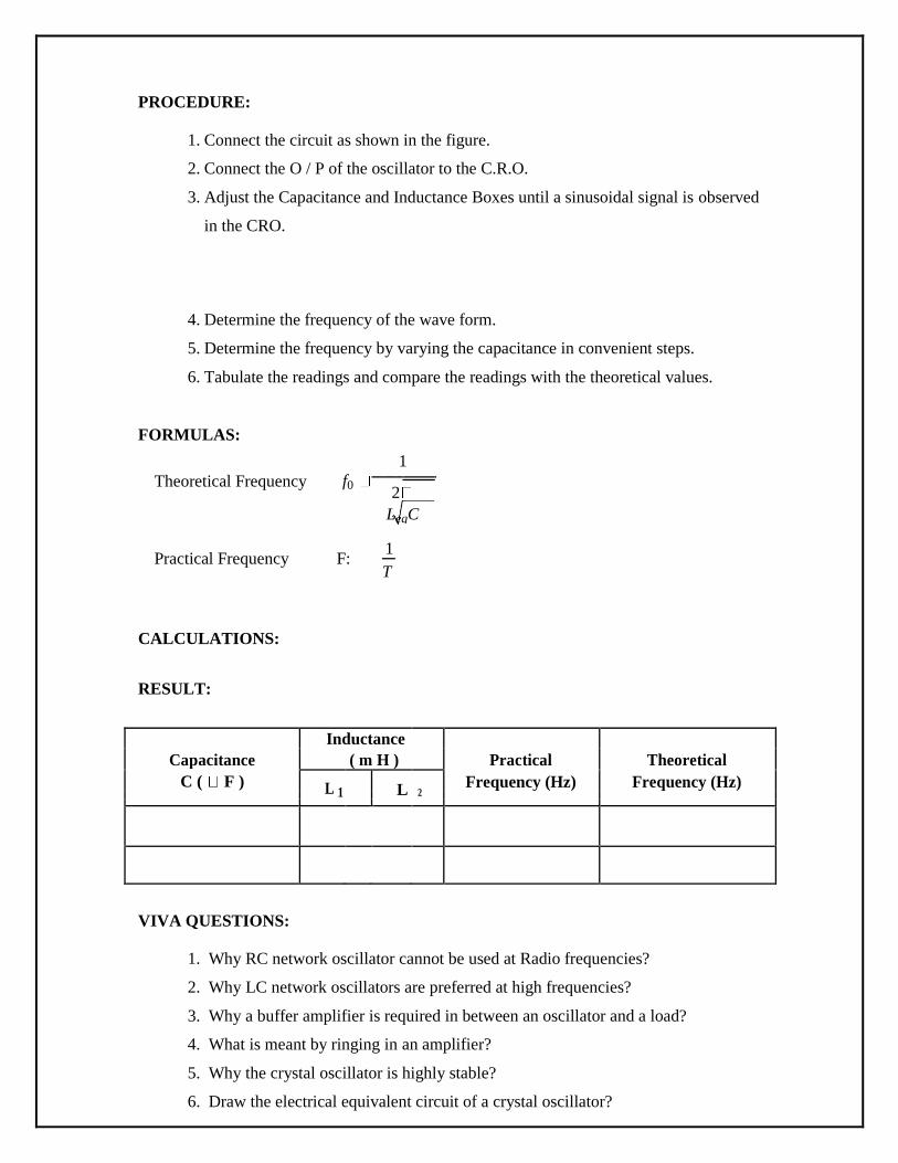
PROCEDURE:
1. Connect the circuit as shown in the figure.
2. Connect the O / P of the oscillator to the C.R.O.
3. Adjust the Capacitance and Inductance Boxes until a sinusoidal signal is observed
in the CRO.
4. Determine the frequency of the wave form.
5. Determine the frequency by varying the capacitance in convenient steps.
6. Tabulate the readings and compare the readings with the theoretical values.
FORMULAS:
Theoretical Frequency f0
1
2
LeqC
Practical Frequency F: 1
T
CALCULATIONS:
RESULT:
Capacitance
Inductance
Practical Theoretical ( m H )
C ( F ) L 1
L 2 Frequency (Hz) Frequency (Hz)
VIVA QUESTIONS:
1. Why RC network oscillator cannot be used at Radio frequencies?
2. Why LC network oscillators are preferred at high frequencies?
3. Why a buffer amplifier is required in between an oscillator and a load?
4. What is meant by ringing in an amplifier?
5. Why the crystal oscillator is highly stable?
6. Draw the electrical equivalent circuit of a crystal oscillator?