edax temple university scott sitzman oxford … university scott sitzman-oxford instruments. 2 ......
TRANSCRIPT
Stuart Wright -
EDAX John Friel
-
Temple University Scott Sitzman
-
Oxford Instruments
2
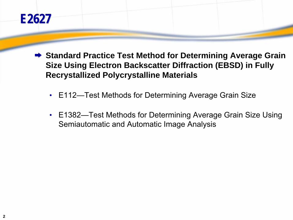
E2627E2627
Standard Practice Test Method for Determining Average Grain Size Using Electron Backscatter Diffraction (EBSD) in Fully Recrystallized Polycrystalline Materials
• E112—Test Methods for Determining Average Grain Size
• E1382—Test Methods for Determining Average Grain Size Using Semiautomatic and Automatic Image Analysis
3
OutlineOutline
Introduction to EBSD
Grain Size using EBSD• Grain grouping algorithm• Tolerance Angle• Minimum point counts• Cleanup
Standard Calculations• Grain size number• Confidence interval & Relative Accuracy• Non-equiaxed structures

4
Motivation – H. Weiland AlcoaMotivation – H. Weiland Alcoa
Given all of the uncertainties associated with conventional graiGiven all of the uncertainties associated with conventional grain size n size measurements can we measure grain size using EBSD? Particularly measurements can we measure grain size using EBSD? Particularly problematic in materials where it is difficult to get good grainproblematic in materials where it is difficult to get good grain
boundary boundary contrast (aluminum).contrast (aluminum).
A. Day (1998). "Is that one grain or two?" Materials World 6: 8-10

5
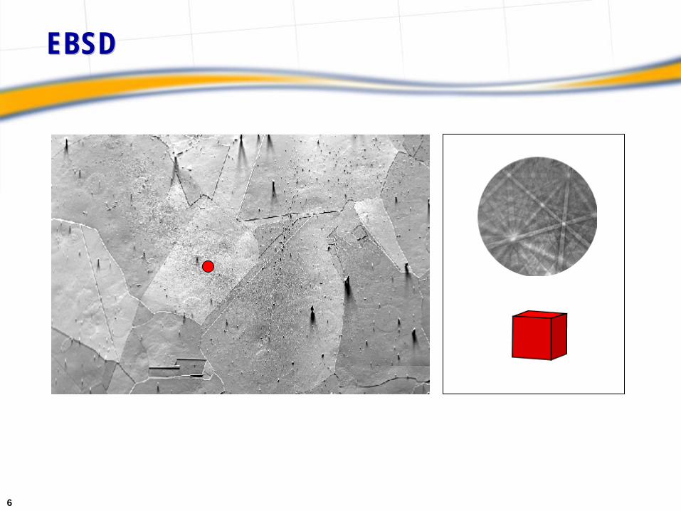
EBSDEBSD
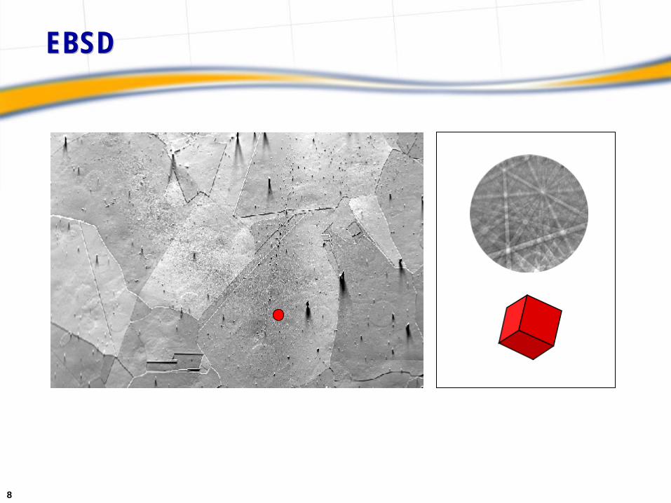
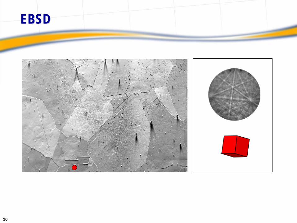
Electron backscatter diffraction patterns (or EBSPs) are obtained in the SEM by focusing a stationary electron beam on a crystalline sample. The sample is tilted to approximately 70 degrees with respect to the horizontal. The diffraction pattern is imaged on a phosphor screen. The image is captured using a low-light CCD camera. The bands in the pattern represent reflecting planes in the diffracting crystal volume. Thus, the geometrical arrangement of the bands is a function of the orientation of the diffracting crystal lattice.
6
EBSDEBSD

7
EBSDEBSD
8
EBSDEBSD

9
EBSDEBSD
10
EBSDEBSD

11
EBSD - HardwareEBSD - Hardware
Phosphor screen
CameraBellows
Slide
12
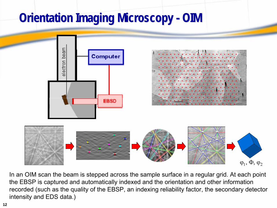
Orientation Imaging Microscopy - OIMOrientation Imaging Microscopy - OIM
In an OIM scan the beam is stepped across the sample surface in a regular grid. At each point the EBSP is captured and automatically indexed and the orientation and other information recorded (such as the quality of the EBSP, an indexing reliability factor, the secondary detector intensity and EDS data.)
13
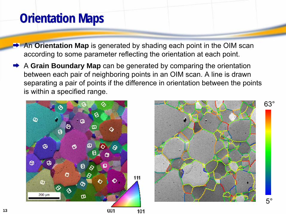
Orientation MapsOrientation Maps
An Orientation Map is generated by shading each point in the OIM scan according to some parameter reflecting the orientation at each point.
5°
63°
A Grain Boundary Map can be generated by comparing the orientation between each pair of neighboring points in an OIM scan. A line is drawn separating a pair of points if the difference in orientation between the points is within a specified range.
14
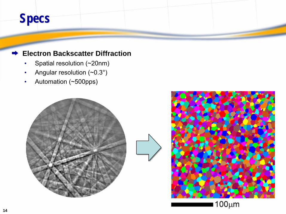
SpecsSpecs
Electron Backscatter Diffraction• Spatial resolution (~20nm)• Angular resolution (~0.3°)• Automation (~500pps)

15
0
100
200
300
400
500
600
700
800
900
1000
1925 1945 1965 1985 2005
EBSD
Pape
rs
Year
Historical OverviewHistorical Overview
1991Wright, Kunze,
Adams & Dingley
1928Kikuchi et al.
1984Dingley et al.
1984Dingley et al.

16
Individual Orientations Measurements to GrainsIndividual Orientations Measurements to Grains

17
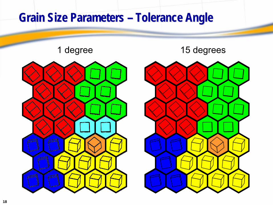
While the concept of a grain in conventional metallography is commonly understood, the definition of a grain in an OIM scan is slightly different . Grains in OIM are formed by an algorithm that groups sets of connected and similarly oriented points into “grains”. For each point in the OIM scan, the neighbors of this point are checked to see if they are within the Grain Tolerance Angle of the given point. If a neighboring point is found to be within the tolerance angle then the neighbors of this point are checked to see if they are within the tolerance angle of this point. The procedure is repeated over and over again until the set of connected grains is bounded by points which exceed the tolerance angle. Using this approach, the point to point misorientation in a “grain”
will be quite small but the spread of orientation among all points in the “grain”
can be relatively large. The number of points required to decide whether a given group of points should be considered a “grain”
group (the Minimum Grain Size) can be specified by the user along with the Grain Tolerance Angle. Thus, the definition of a grain in OIM can vary depending on user-specified values.
“Grains” in OIM“Grains” in OIM
18
Grain Size Parameters – Tolerance AngleGrain Size Parameters – Tolerance Angle
1 degree 15 degrees

19
Grain Size Parameters – Min Grain SizeGrain Size Parameters – Min Grain Size
2 “Pixels” 5 “Pixels”

20
Non-Indexed and Mis-Indexed PointsNon-Indexed and Mis-Indexed Points

21
Non-indexed points - Rough SurfacesNon-indexed points - Rough Surfaces
Here is the SED and a map from a Zinc coating on steel. Due to the surface roughness and topography we cannot expect usable EBSD patterns everywhere in this area.
22
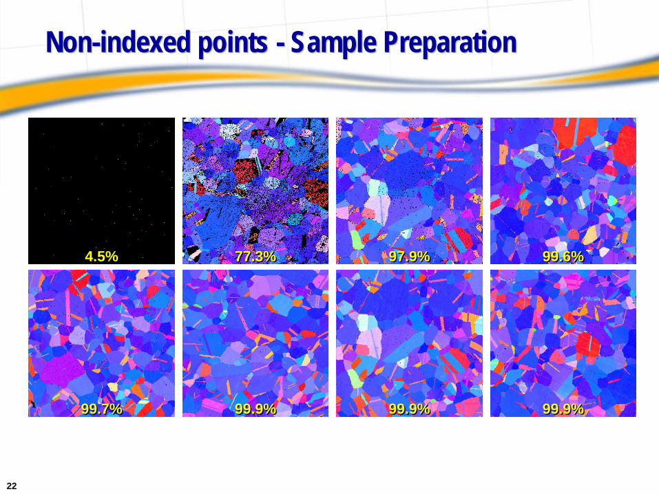
Non-indexed points - Sample PreparationNon-indexed points - Sample Preparation
4.5%4.5% 77.3%77.3% 97.9%97.9% 99.6%99.6%
99.7%99.7% 99.9%99.9% 99.9%99.9% 99.9%99.9%
23
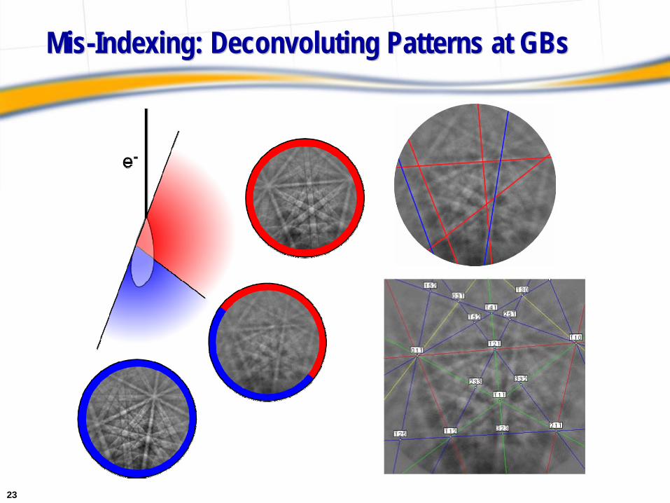
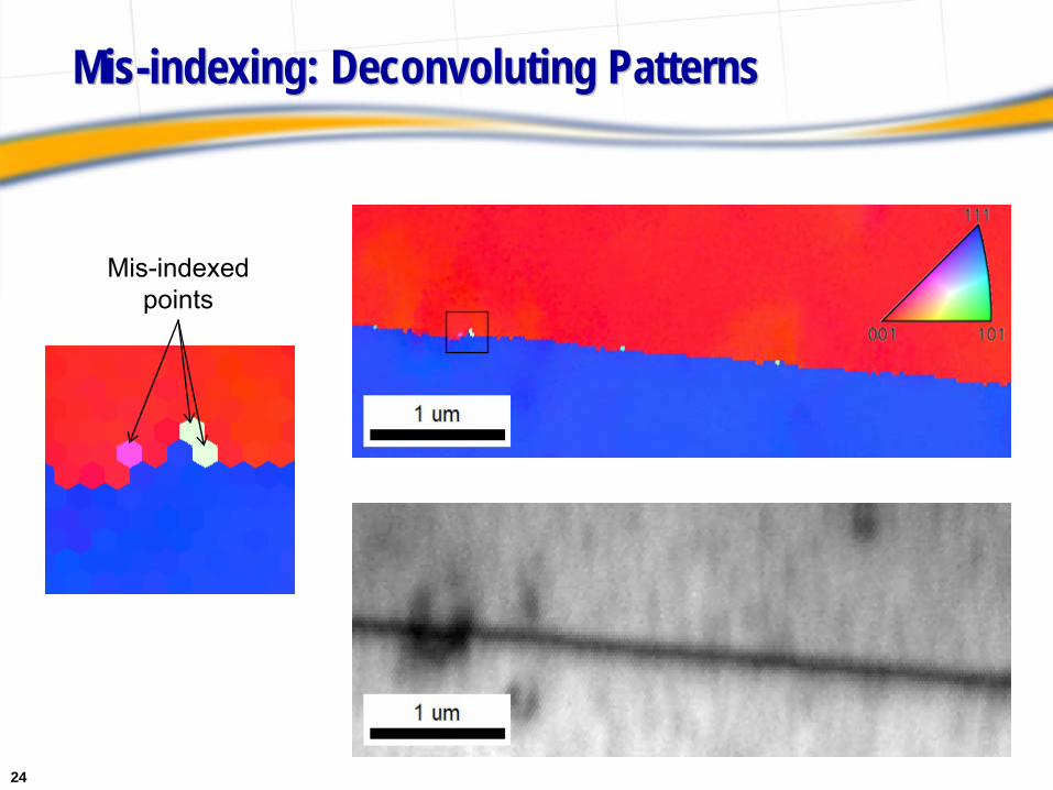
Mis-Indexing: Deconvoluting Patterns at GBsMis-Indexing: Deconvoluting Patterns at GBs
24
Mis-indexing: Deconvoluting PatternsMis-indexing: Deconvoluting Patterns
Mis-indexed points

25
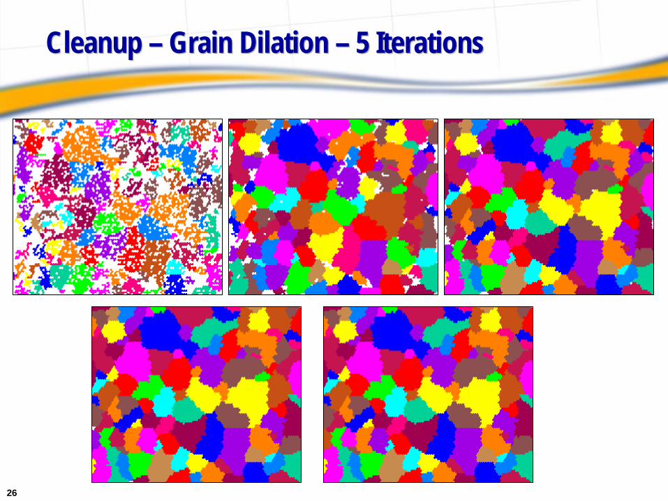
Cleanup: Grain DilationCleanup: Grain Dilation
This clean up method is an iterative method. The routine only acts on points that do not belong to any grains; yet have neighboring points, which do belong to grains. A point may not belong to any grain due to the point either not being indexed or due to it belonging to a grain group having fewer members than the Minimum Grain Size. If the majority of neighbors of a particular point belong to the same grain then the orientation of the particular point is changed to match that
of the majority grain -
otherwise the orientation is randomly changed to match any of the neighboring points, which belong to grains. This process is repeated until each point in the data set becomes a member of a grain. (Alternatively, the user may set the code to only perform a single iteration.) In the schematic below, in the left hand figure the data point in white is not part of any grains. After dilation it's orientation is changed to match that of the neighboring green grain.
26
Cleanup – Grain Dilation – 5 IterationsCleanup – Grain Dilation – 5 Iterations

27
Mis-indexing & Non-Indexing: CleanupMis-indexing & Non-Indexing: Cleanup
FullCleanup
28
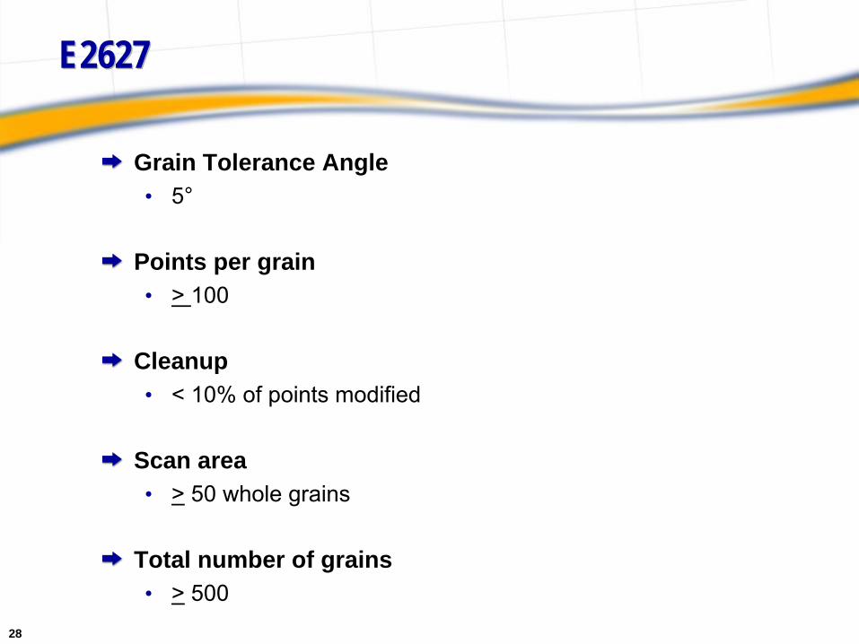
E2627E2627
Grain Tolerance Angle• 5°
Points per grain• > 100
Cleanup• < 10% of points modified
Scan area• >
50 whole grains
Total number of grains• >
500

29
Grain Size Calculation EquationsGrain Size Calculation Equations
Square Grid:
Hexagonal Grid:
Average Area:
Standard deviation:
Grain Size Number (in mm2):
Grain Size Number (in m2):
2
23
ii PA
2 ii PA
i
N
iA
NA
1
1
995.2log3223.3 AG
995.210log3223.3 6 AG
21
1
2
11
N
ii AA
Ns
30
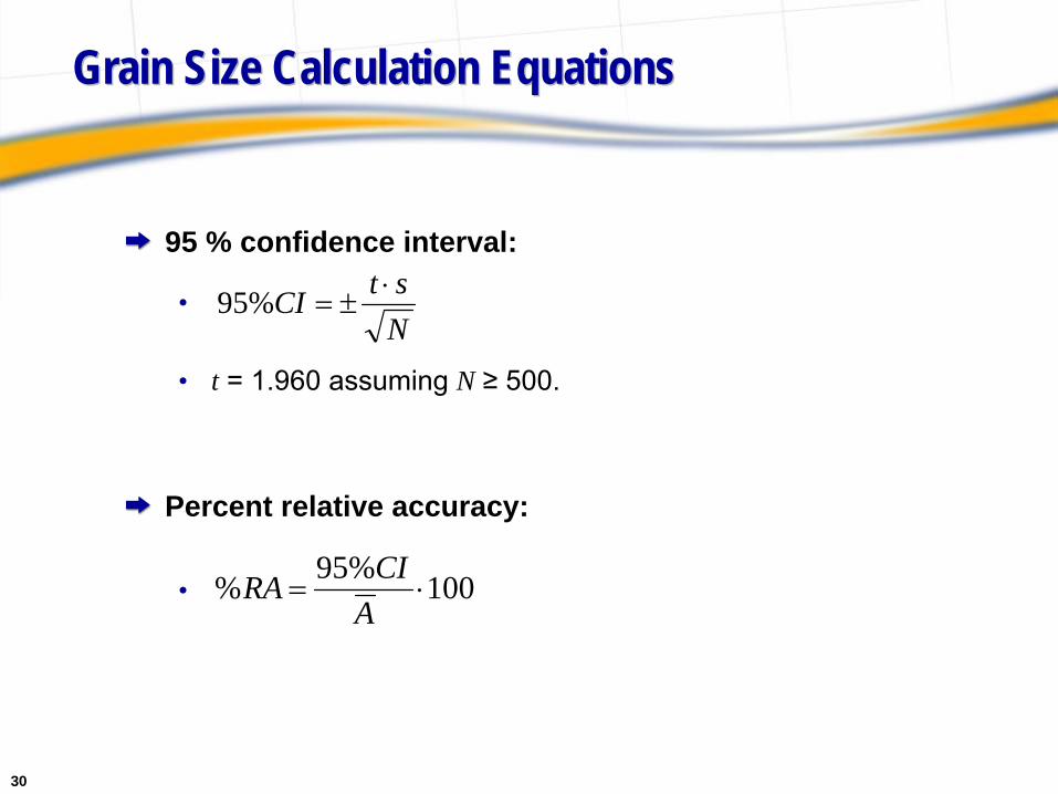
Grain Size Calculation EquationsGrain Size Calculation Equations
95 % confidence interval:
•
• t = 1.960 assuming N ≥
500.
Percent relative accuracy:
• 100%95% A
CIRA
NstCI
%95

31
E2627E2627
Standard Practice Test Method for Determining Average Grain Size Using Electron Backscatter Diffraction (EBSD) in Fully Recrystallized Polycrystalline Materials
235.0 mA 233.0 ms
G = 18.512% cleanup2654 grains

32
EBSD vs. Optical MethodsEBSD vs. Optical Methods
+ Resolution• ~500 nm• 100 points per grain limits ultimate resolution due to charge build-up on the
sample• Can be implemented on most SEMs
± Quantitative Grain Boundary Identification• + no need for erosion or watershed image processing techniques• + Particularly helpful in materials where good grain boundary contrast is difficult
to achieve• -
difficult to identify the “correct”
value for deformed materials+ Other microstructural information
• Crystallographic orientation and misorientation (texture)• Material state (strain)
- Costs• SEM + EBSD system• Technical expertise• Sample prep

33
Why Recrystallized Materials Only?Why Recrystallized Materials Only?
± Quantitative Grain Boundary Identification
2°
tolerance angle15°
tolerance angleEqual Channel Angular Extrusion