economic impact of measurement in the semiconductor industry
TRANSCRIPT
Planning Report 07-2
Economic Impact of Measurement in the Semiconductor Industry
Prepared by: RTI International
for
National Institute of Standards & Technology
December 2007
December 2007
Economic Impact of Measurement in the Semiconductor Industry
Final Report
Prepared for
Gregory C. Tassey National Institute for Standards and Technology
100 Bureau Drive, Stop 1060 Gaithersburg, MD 20899-1060
Prepared by
Michael P. Gallaher Brent R. Rowe
Alex V. Rogozhin Stephanie A. Houghton
J. Lynn Davis Michael K. Lamvik
John S. Geikler RTI International
3040 Cornwallis Road Research Triangle Park, NC 27709
RTI Project Number 0209878.000
_________________________________
RTI Project Number 0209878.000
Economic Impact of Measurement in the Semiconductor Industry
Final Report
December 2007
Prepared for
Gregory C. Tassey National Institute for Standards and Technology
100 Bureau Drive, Stop 1060 Gaithersburg, MD 20899-1060
Prepared by
Michael P. Gallaher Brent R. Rowe
Alex V. Rogozhin Stephanie A. Houghton
J. Lynn Davis Michael K. Lamvik
John S. Geikler RTI International
3040 Cornwallis Road Research Triangle Park, NC 27709
RTI International is a trade name of Research Triangle Institute
Contents
Section Page
Executive Summary ES-1
1 Introduction 1-1
1.1 The Importance of Measurement in the Semiconductor Industry.........................................................................................1-2
1.2 Project Scope and Goals .............................................................1-3
1.2.1 Measurement versus Metrology......................................1-4
1.2.2 Important Project Scope Parameters..............................1-5
1.2.3 Key Study Objectives ......................................................1-5
1.3 Report Organization .....................................................................1-6
2 Overview of the Semiconductor Industry 2-1
2.1 Role of Semiconductors ...............................................................2-2
2.2 How Semiconductors Are Made...................................................2-3
2.3 Stakeholders in the Semiconductor Industry ...............................2-7
2.4 Measurement Categories: A Taxonomy ......................................2-8
3 Advances in Measurement in the Semiconductor Industry 3-1
3.1 A Decade of Changes in Measurement .......................................3-3
3.1.1 The Impetus for Increased Measurement Investment.......................................................................3-3
3.1.2 Key Measurement Initiatives and Roadmaps .................3-6
3.2 Product Design Tools...................................................................3-7
3.2.1 System Design Tools ......................................................3-8
3.2.2 Design for Manufacturability............................................3-8
3.2.3 Device and Process Simulation ......................................3-9
3.2.4 Product Life-Cycle Management.....................................3-9
3.3 Software Standards and Interoperability......................................3-9
3.3.1 Verification Languages..................................................3-10
3.3.2 Data Formats ................................................................3-10
iii
4
3.4 Calibration and Standard Test Methods ....................................3-11
3.5 Ex Situ Process Control Technology .........................................3-13
3.5.1 CD Measurement ..........................................................3-13
3.5.2 Thin-Film Thickness Measurement...............................3-14
3.5.3 Thin-Film Composition ..................................................3-14
3.5.4 Thin-Film Structure........................................................3-15
3.6 In Situ Process Control Technology...........................................3-15
3.6.1 Off-Wafer In Situ Process Control.................................3-16
3.6.2 On-Wafer In Situ Process Control.................................3-16
3.7 Quality Assurance ......................................................................3-17
3.7.1 Chemical and Materials Suppliers ................................3-18
3.7.2 Front-End Processing Firms .........................................3-19
3.7.3 Back-End Processing Firms..........................................3-20
Assessing the Impacts of Measurement Improvements
4.1 Approach Overview: Arriving at a Counterfactual Scenario.........4-1
4.1.1 Establishing the Period of Analysis.................................4-2
4.1.2 Estimating Benefits and Costs Relative to the Measurement Paradigm in Place in 1996.......................4-3
4.2 Estimating Measurement Expenditures, 1996 to 2006 ................4-3
4.2.1 Technology Adoption ......................................................4-4
4.2.2 Normalization and Extrapolation of Survey Responses ......................................................................4-5
4.2.3 Expenditure Categories...................................................4-6
4.2.4 Fixed versus Variable Expenditures ...............................4-6
4.3 Quantifying Economic Benefits from Improved Measurement, 1996 to 2011 ........................................................4-9
4.3.1 Lower Scrap and Rework Rates .....................................4-9
4.3.2 Quality Improvements ...................................................4-11
4.3.3 Benefits Estimation Calculation ....................................4-13
4.3.4 Benefits Accrual by Stakeholder Group ........................4-14
4.4 Calculating Measures of Economic Return................................4-14
4.4.1 Benefit-to-Cost Ratio.....................................................4-15
4.4.2 Net Present Value .........................................................4-15
4.4.3 Internal Rate of Return..................................................4-16
4.5 Data Collection Activities............................................................4-16
4.5.1 Telephone and On-Site Interviews................................4-16
4.5.2 Internet-Based Survey Data Collection.........................4-17
4.5.3 Secondary Data Collection............................................4-17
4.5.4 Data Collection Challenges...........................................4-17
iv
4-1
5 Measurement Technology Adoption and Expenditures 5-1
5.1 Summary Expenditure and Adoption Data, 1996 to 2006 ...........5-1
5.1.1 Inflation-Adjusted Industry Sales Revenues ...................5-1
5.1.2 Industry Expenditures .....................................................5-2
5.1.3 Expenditures by NIST and Industry Consortia................5-6
5.1.4 Time Series of Industry and Consortia Expenditures ...................................................................5-8
5.2 Detailed Expenditure and Adoption Data by Measurement Category, 1996 to 2006................................................................5-8
5.2.1 Product Design Tools....................................................5-10
5.2.2 Calibration and Standard Test Methods .......................5-13
5.2.3 Ex Situ Process Control ................................................5-16
5.2.4 In Situ Process Control .................................................5-20
5.2.5 Quality Assurance .........................................................5-25
6 Economic Benefits from Measurement Improvements 6-1
6.1 Benefit Estimates by Cost Category ............................................6-2
6.1.1 Rework Improvements ....................................................6-4
6.1.2 Scrap Improvements .......................................................6-5
6.2 Benefits by Measurement Category.............................................6-7
6.2.1 Product Design Tools......................................................6-7
6.2.2 Software Standards and Interoperability.........................6-8
6.2.3 Calibration and Standard Test Methods .........................6-9
6.2.4 Ex Situ Process Control ..................................................6-9
6.2.5 In Situ Process Control ...................................................6-9
6.2.6 Quality Assurance ...........................................................6-9
6.3 Measures of Economic Return.....................................................6-9
6.3.1 Time Series of Costs and Benefits..................................6-9
6.3.2 Performance Measures.................................................6-10
6.4 Uncertainties and Data Limitations ............................................6-14
7 Conclusion 7-1
7.1 Economic Returns from Coordinated Measurement R&D Strategy ........................................................................................7-1
7.2 Stakeholders’ Views on Opportunities for NIST...........................7-3
References R-1
v

Appendixes
A: Expanded Technical Discussion .......................................................A-1
B: Survey Instrument .............................................................................B-1
vi
Figures
Number Page ES-1 Semiconductor Industry Supply Chain and Major Process Flows...... ES-4 ES-2 Overview of the Roles of Measurement in Semiconductor Design
3-1 Overview of the Roles of Measurement in Semiconductor Design
4-3 General Measurement Expenditure Trends over Time, Variable
5-1 Change in Inflation-Adjusted Semiconductor Industry Sales
5-2 Annual Measurement Expenditures by Stakeholder Group,
5-3 Annual Measurement Expenditures by Measurement Category,
6-2 Total Annual Benefits by Measurement Category, 1996–2011
6-3 Cumulative Expenditures and Benefits from Measurement
6-4 Annual Expenditures and Benefits of Measurement, 1996–2011
and Production.................................................................................... ES-6
ES-3 Simplified Economic Impact Assessment Steps................................. ES-7
ES-4 Key Benefit Metrics: Scrap and Rework ............................................. ES-8
2-1 Semiconductor Industry Supply Chain and Major Process Flows.........2-4
and Production.......................................................................................3-2
3-2 Reductions in Wafer and Feature Sizes, 1996–2006 ............................3-4
4-1 Simplified Impact Assessment Steps.....................................................4-2
4-2 Stakeholder Group-Measurement Category Combinations...................4-7
versus Fixed...........................................................................................4-8
4-4 Key Benefit Metrics: Scrap and Rework ................................................4-9
4-5 General Benefit Trends over Time by Category ..................................4-10
Revenue, Americas and Worldwide, 1996–2006 (millions) ...................5-3
1996–2006 (millions)..............................................................................5-5
1996–2006 (millions)..............................................................................5-5
6-1 Annual Economic Benefits by Type, 1996–2011 (millions) ...................6-4
(millions).................................................................................................6-8
Improvements, 1996–2011 (millions)...................................................6-12
(millions)...............................................................................................6-12
vii

Tables
Number Page
ES-1 Total Measurement Expenditures by Measurement Category and Stakeholder Group, 1996–2006........................................................ ES-10
ES-3 Performance Metrics for Investments in Measurement, 1996–
2-2 U.S. Semiconductor Revenue by Stakeholder Group, 1996 and
5-1 Change in Inflation-Adjusted Semiconductor Industry Sales
5-2 Inflation-Adjusted Semiconductor Industry Sales Revenues by
5-3 Total Measurement Expenditures by Measurement Category and
5-4 Percentage Spending on Fixed Cost Measurement
5-5 Annual Fixed and Variable Measurement Expenditures, 1996–
5-7 Industry and Consortia Measurement Expenditures, 1996 to
5-9 Adoption of Product Design Tools by IC Design Firms, 1996–
5-10 Expenditures on Software Standards and Interoperability by
5-11 Adoption of Graphic Data System (GDSII, GDSIII, and GDSIV)
5-12 Expenditures on Calibration and Standard Test Methods by
ES-2 Time Series of Benefits by Type, 1996–2011................................... ES-11
2011 .................................................................................................. ES-12
2-1 Examples and Uses of Semiconductor Devices ....................................2-3
2006 .......................................................................................................2-9
3-1 Relative Measurement Needs by Device Type......................................3-6
Revenue by Stakeholder Group, 1996 and 2006 ..................................5-2
Stakeholder Group, 1996–2006.............................................................5-3
Stakeholder Group, 1996–2006.............................................................5-4
Improvements in 1996, 2001, and 2006 ................................................5-6
2011 .......................................................................................................5-7
5-6 Expenditures by Major R&D Organizations, 1996–2006 .......................5-7
2011 .......................................................................................................5-9
5-8 Relevance of Measurement Categories to Stakeholder Groups .........5-10
2006 .....................................................................................................5-11
Stakeholder Group, 1996–2006...........................................................5-12
by Stakeholder Group, 1996–2006......................................................5-14
Stakeholder Group, 1996–2006...........................................................5-14
viii
5-13 Adoption of Reference Materials for Resistivity, Particle Count, Thickness, or Other Measurements by Stakeholder Group, 1996–2006 ...........................................................................................5-15
5-14 Expenditures on Ex Situ Process Control by Stakeholder Group,
5-15 Adoption of Ex Situ Technologies by Stakeholder Group, 1996–
5-16 Expenditures on In Situ Process Control by Stakeholder Group,
5-17 Adoption of In Situ Technologies by Stakeholder Group, 1996–
5-18 Expenditures on Quality Assurance Techniques by Stakeholder
5-19 Adoption of Quality Assurance Technologies by Stakeholder
6-4 Percentage Attribution of Benefits by Measurement Category,
6-5 Total Cumulative Benefits by Measurement Category, 1996–
6-8 Performance Metrics for Investments in Measurement, 1996–
6-9 Percentage Attribution of Quality Benefits by Measurement
7-1 Performance Metrics for Investments in Measurement, 1996–
1996–2006 ...........................................................................................5-16
2006 .....................................................................................................5-18
1996–2006 ...........................................................................................5-21
2006 .....................................................................................................5-23
Group, 1996–2006 ...............................................................................5-25
Group, 1996–2006 ...............................................................................5-27
6-1 Time Series of Benefits by Type, 1996–2011........................................6-3
6-2 Annual Benefits from Improved Rework Rates, 1996–2011..................6-5
6-3 Annual Benefits from Improved Scrap Rates, 1996–2011 ....................6-6
1996–2011 .............................................................................................6-7
2011 .......................................................................................................6-8
6-6 Summary Cost and Benefit Figures, 1996–2011.................................6-11
6-7 Net Benefit Calculation by Measurement Category.............................6-13
2011 .....................................................................................................6-13
Category, 1996–2006 ..........................................................................6-13
2011 .......................................................................................................7-3
ix
Executive Summary
The semiconductor industry has long been a driving force behind major advances in computing and electronics. Advances in the speed of processing power have enabled individuals and companies to create, access, and analyze data rapidly, improving individual and business efficiency and developing new markets within the national and global economies.
Between 1996 and 2006, semiconductor manufacturers and semiconductor technology research groups, including the National Institute of Standards and Technology (NIST) and industry consortia, made significant investments in the technology infrastructure that supports the industry. The novel measurement equipment, software, and systems they created accelerated the development of less expensive, higher quality semiconductors that enable the production of products as varied as lighting systems and computers. Without these investments, the industry would have otherwise been less efficient, incurring higher defect rates and greater costs, all of which would have been passed along to consumers through higher prices, lower product quality, and slower processing speed.
The goal of this study was to quantify the investment made by the semiconductor industry, government, and consortia in the measurement infrastructure between 1996 and 2006 and to compare that estimate with the economic benefits firms accrued as a consequence. This study also analyzed the trends catalyzing a broad-based, public–private strategy for improving the industry’s measurement capabilities and thereby the industry’s competitiveness in the global market.
ES-1

Economic Impact of Measurement in the Semiconductor Industry
ES.1
ES.1.1
ES.1.2
PROJECT SCOPE AND GOALS Since the 1970s, the semiconductor industry has focused on continually satisfying “Moore’s Law,” the prediction made by Gordon Moore, cofounder of Intel, that the number of transistors per chip in a semiconductor device would double every 2 years. As time progressed, however, achieving that benchmark became more challenging. By the early 1990s, the semiconductor industry was largely focused on making incremental advances in the quality of their products. It soon became apparent that the way forward was rooted in exploiting the potential of nanoscale measurement opportunities.
Advances in measurement technology are often credited with helping the industry keep up with Moore’s Law between 1996 and 2006, during which time the number of possible transistors per logic chip increased from 3.1 million in 1994 to 1.7 billion in 2005 (SIA, 2005). Several industry associations and research groups facilitated industry collaboration through the National Technology Roadmap for Semiconductors (NTRS) in 1992. The NTRS focused on developing measurement technologies and standards that could leverage the entire U.S. semiconductor industry. Many factors helped the industry realize its achievements, but without the strategic work done under the NTRS and its successors, the International Technology Roadmap for Semiconductors (ITRS), many of these achievements would not have been possible.
Study Background
The NIST Program Office sponsored this research for two reasons. As a purely retrospective investment analysis, NIST is interested in the impact that advances in standardization and measurement technologies have had on the semiconductor industry. This analysis is also important for both NIST and companies throughout the industry as part of strategic planning processes. Analyzing past impacts and future needs can help the industry and supporting bodies such as NIST focus attention and investment dollars on measurement issues projected to be most significant and show substantive returns from past investments.
Study Objectives
This study assessed the net benefits of improvements to the measurement infrastructure supporting the semiconductor industry between 1996 and 2006. To this end, it focused on the incremental
ES-2
Executive Summary
adoption of and associated investments in measurement technologies and standards and the economic impact these developments have had on the industry. Specifically, the main objectives of this study were to
• describe and assess the economic roles of the technology infrastructure that supports the semiconductor industry,
• quantify industry investments in measurement-related infratechnologies over the past 10 years, and
• quantify the collective benefit that advances in measurement over the past 10 years have had on the semiconductor industry in terms of growth and competitiveness.
ES.2 MEASUREMENT ADVANCES IN THE SEMICONDUCTOR SUPPLY CHAIN, 1996 TO 2006 Semiconductor materials are characterized by having intermediate electrical conductivity properties between those of metallic conductors and insulators. Semiconductor materials are used to fabricate electronic devices, such as transistors and diodes (e.g., light-emitting diodes, or LEDs). These devices relay, switch, or amplify electricity and permit electrical devices to function as intended. Producing semiconductor-based devices involves converting a variety of materials (e.g., gases, liquids, and metals) into either a single discrete device, with a single function, or an “integrated circuit,” which combines many functions into one semiconductor device.
ES.2.1 The Semiconductor Supply Chain
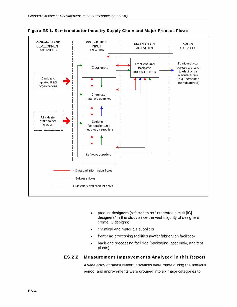
Semiconductor production requires firms to coordinate their R&D, manufacturing, data analysis, and marketing transactions efficiently. Figure ES-1 provides an overview of the industry stakeholders’ collaboration through three process flows: (1) data and information, (2) software products, and (3) physical products (i.e., raw chemicals and materials and final products).
For the purpose of this study, firms in the semiconductor supply chain were categorized into stakeholder groups for which expenditures and benefits were estimated:
• basic and applied R&D organizations
• equipment and software suppliers
ES-3
Economic Impact of Measurement in the Semiconductor Industry
Figure ES-1. Semiconductor Industry Supply Chain and Major Process Flows
Basic and applied R&D organizations
All industry stakeholder
groups
IC designers Front-end and
back-end processing firms
Chemical/ materials suppliers
Equipment (production and
metrology ) suppliers
Software suppliers
Semiconductor devices are sold
to electronics manufacturers (e.g., computer manufacturers)
RESEARCH AND DEVELOPMENT
ACTIVITIES
PRODUCTION INPUT
CREATION
PRODUCTION ACTIVITIES
SALES ACTIVITIES
= Data and information flows
= Software flows
= Materials and product flows
• product designers (referred to as “integrated circuit [IC] designers” in this study since the vast majority of designers create IC designs)
• chemical and materials suppliers
• front-end processing facilities (wafer fabrication facilities)
• back-end processing facilities (packaging, assembly, and test plants)
ES.2.2 Measurement Improvements Analyzed in this Report
A wide array of measurement advances were made during the analysis period, and improvements were grouped into six major categories to
ES-4

Executive Summary
keep the study scope manageable while ensuring effective coverage of significant impact categories. The categories were developed according to industry goals outlined in technology roadmaps that set cross-industry agendas to develop standards and generic technologies. The categories included traditional standard and measurement science as well as measurement-related areas like standard data formats and analytical measures:
• product design tools
• software standards and interoperability
• calibration and standard test methods
• ex situ process control techniques
• in situ process control techniques
• quality assurance
Figure ES-2 provides several examples for each of the six categories listed above, as well as an overview of how the categories relate to industry stakeholder groups. The figure focuses on the design and production process for a semiconductor chip; thus, it does not include supporting organizations such as consortia or other groups involved in process R&D, though their research was integral to the industry’s success in developing advanced measurement systems.
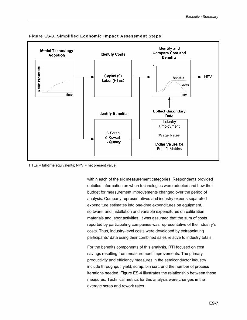
ES.3 METHODOLOGY FOR QUANTIFYING BENEFITS AND COSTS As shown in Figure ES-3, industry-level economic impact estimates were calculated by combining technology adoption curves with cost and benefit metrics and secondary data. This report provides impact estimates for each measurement category as well as for each stakeholder group. Information on technology adoption was collected through an Internet survey to determine when firms began to incorporate technologies and how diffusion progressed over time.
The data employed in this analysis were collected using three modes: in-person and telephone interviews, Internet-based surveys, and a review of secondary data sources. Ultimately, the companies that provided information represented 82% of the semiconductor industry, as measured by 2006 industry revenues.
Respondents provided data on their spending on measurement improvements and process changes adopted between 1996 and 2006
ES-5
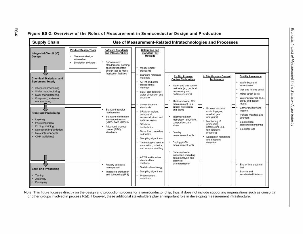
ES-6 Figure ES-2. Overview of the Roles of Measurement in Semiconductor Design and Production
Supply Chain
Integrated Circuit (IC) Design
Chemical, Materials, and Equipment Supply
• Chemical processing • Wafer manufacturing • Mask manufacturing • Equipment, software
manufacturing
Front-End Processing
• Layering • Photolithography • Etching, striping • Doping/ion implantation • Metal interconnects • CMP (polishing)
Back-End Processing
• Testing • Assembly • Packaging
Use of Measurement-Related Infratechnologies and Processes Product Design Tools
• Electronic design automation
• Simulation software
Ex Situ Process Control Technology
• Water and gas control methods (e.g., optical microscopy and particle counters)
• Mask and wafer CD measurement (e.g., optical microscopy and SEM)
• Thermal/thin film metrology—structure, composition, and stress
• Overlay measurement tools
• Doping profile measurement tools
• Patterned wafer inspection, including defect analysis and electrical characterization
Calibration and Standard Test
Methods
• Measurement standards
• Standard reference materials
• ASTM and other standard test methods
• SEMI standards for wafer dimension and structure
• Linear distance standards
• SRMs for wafers, compound semiconductors, and epitaxial layers
• SRMs for implantation
• Mass flow controllers calibration
• Sampling algorithms
• Technologies used in automation, robotics, and sample handling
• ASTM and/or other standard test methods
• Statistical metrology
• Sampling algorithms
• Probe contact variations
Software Standards and Interoperability
• Software and standards for passing specifications from design labs to mask fabrication facilities
• Standard transfer mechanisms
• Standard information exchange formats (IGES, DXF, GDS II)
• Advanced process control (APC) standards
• Factory database management
• Integrated production and scheduling (IPS)
Quality Assurance
• Wafer bow and smoothness
• Gas and liquids purity
• Metal target purity
• Wafer properties (e.g., purity and dopant levels)
• Carrier mobility and lifetime
• Particle monitors and counters
• Electrostatic discharge monitoring
• Electrical test
• End-of-line electrical test
• Burn-in and accelerated life tests
In Situ Process Control Technology
• Process vacuum control (gages, residual gas analyzers)
• Monitoring of processing parameters (e.g., temperature, pressure)
• Deposition monitoring and endpoint detection
Econom
ic Impact of M
easurement in the S
emiconductor Industry
Note: This figure focuses directly on the design and production process for a semiconductor chip; thus, it does not include supporting organizations such as consortia or other groups involved in process R&D. However, these additional stakeholders play an important role in developing measurement infrastructure.
Executive Summary
Figure ES-3. Simplified Economic Impact Assessment Steps
FTEs = full-time equivalents; NPV = net present value.
within each of the six measurement categories. Respondents provided detailed information on when technologies were adopted and how their budget for measurement improvements changed over the period of analysis. Company representatives and industry experts separated expenditure estimates into one-time expenditures on equipment, software, and installation and variable expenditures on calibration materials and labor activities. It was assumed that the sum of costs reported by participating companies was representative of the industry’s costs. Thus, industry-level costs were developed by extrapolating participants’ data using their combined sales relative to industry totals.
For the benefits components of this analysis, RTI focused on cost savings resulting from measurement improvements. The primary productivity and efficiency measures in the semiconductor industry include throughput, yield, scrap, bin sort, and the number of process iterations needed. Figure ES-4 illustrates the relationship between these measures. Technical metrics for this analysis were changes in the average scrap and rework rates.
ES-7

Economic Impact of Measurement in the Semiconductor Industry
Figure ES-4. Key Benefit Metrics: Scrap and Rework
Processing Step
(e.g., deposition, lithography, etch, ion implantation)
Defects created or carried over from previous
steps
Reworkb
Defective wafers sent back to be
reprocessed and corrected
Scrap Defective
wafers discarded
Lot of 25 wafers
Potentially ~12,500 chips, assuming 500
dice per wafera
Yield Percentage of
known good die per wafer
Metrology Step
Defects detected
End - of- Line Testing
Individual die (chip) tested for
performance
Bin Sort Separation of
individual chips according to speed
or other quality measure
Additional processing
and metrology
steps
Measures of Productivity Used in Wafer Processing
aThe number of dice per wafer varies greatly depending on the wafer’s diameter and the size of the chips to be produced. Some designs may have only 40 dice per wafer, while others have more than 500.
bSome wafers are also returned from customers (usually in large batches) and in some cases are “reworked” or sent back through processing to be corrected.
Respondents were asked to identify the level of sales that corresponded to the expenditure data they provided. Aggregated expenditures were divided by respondents’ aggregated revenues to derive the average expenditure per unit of revenue. Because it was known which stakeholder group and technology area participants were responding, it was possible to estimate total expenditures for those groups. It was assumed that the average per unit of revenue estimate was representative of an average stakeholder and thus was multiplied by total stakeholder-level revenues to estimate expenditures. Total industry expenditures were the sum of all stakeholder group estimates. This same procedure was used to extrapolate benefits estimates from the survey response panel to the industry.
ES.4 ECONOMIC COSTS AND BENEFITS FROM MEASUREMENT IMPROVEMENTS Firms decide to make new investments based on an expected rate of return, and investments in measurement standards, equipment, and
ES-8
Executive Summary
process improvements are no different. In general, all benefits from investments in measurement in the semiconductor industry can be thought of as achieving lower costs of production, better products, and accelerated time to market. While expenditures were incurred by all stakeholders, front-end and back-end firms observed the most easily quantifiable positive rate of return on their investments in measurement improvements.
As described throughout this report, the semiconductor industry collaborated extensively, particularly over the past 10 to 15 years as they worked to increase product quality through technology innovation and standardization. In some cases, firms that provided inputs to front-end and back-end processing firms were motivated more by customer and industry pressure than the results of financial analyses (e.g., return on investment calculations) in determining whether an investment should be made. These suppliers have made investments primarily to remain competitive; in other words, they estimated a return on investment in the form of anticipated future sales rather than cost savings. Thus, any resulting cost savings are merely an added benefit. In contrast, front-end and back-end firms have reaped substantive, relatively easily quantifiable positive returns on their investments, which are quantified in this analysis.
In our interviews, study participants described significant cost savings from two main advances—improved yields (decreased scrap) and throughput (decreased rework)—based on the industry’s investments in measurement between 1996 and 2006.
ES.4.1 Measurement Improvements Expenditures
Measurement expenditures differed significantly by stakeholder group and measurement category (see Table ES-1). Front-end processing firms incurred the majority of expenditures, with back-end firms spending the second most. Spending on measurement categories showed that quality assurance, ex situ process control, and in situ process control represent approximately half of total spending.
ES-9

Economic Impact of Measurement in the Semiconductor Industry
Table ES-1. Total Measurement Expenditures by Measurement Category and Stakeholder Group, 1996–2006
Stakeholder Software Calibration Ex Situ In Situ Group/ Product Standards and and Process Process Quality
Measurement Design Interoperability Standards Control Control Assurance Total Category (millions) (millions) (millions) (millions) (millions) (millions) (millions)
R&D organizations — — — — — — $3,276.54
IC design firms $145.66 $64.16 — — — — $209.82
Chemical/materials — — $0.93 — — $27.50 $28.43 suppliers
Equipment suppliers — — $177.11 — — $43.30 $220.41
Front-end — $219.11 $2,601.24 $196.55 $1,346.54 $2,265.36 $6,628.80 processing firms
Back-end — — $26.09 $473.56 $1,082.17 $402.16 $1,983.99 processing firms
Total $145.66 $283.27 $2,805.37 $670.11 $2,428.71 $2,738.32 $12,347.99
Source: RTI estimates. Note: All dollar values are denominated in inflation-adjusted, or real, 2006 dollars.
ES.4.2 Economic Benefits from Measurement Improvements
This study presents quantified cost-saving benefits in two categories:
• reduction in the number of reworked units sent back from customers or by an internal QA department
• reduction in the number of units “scrapped” based on errors in production
Cost saving benefits accrued between 1996 and 2006, and prospective benefits that are estimated to accrue through 2011 include
• better product design tools to prevent hardware errors from ever occurring,
• better software standards and interoperability standards that allow designs to move more quickly within a manufacturing facility and between design and production,
• calibration techniques and quality assurance techniques to ensure precision of inputs and outputs more efficiently,
• new ex situ products allowing more robust measurements to be taken, and
• new in situ products allowing real-time analysis.
Study participants estimated the relative percentage of each cost-saving benefit that would be realized by their own stakeholder group. The time series of benefits by benefit category is provided in Table ES-2, depicting
ES-10
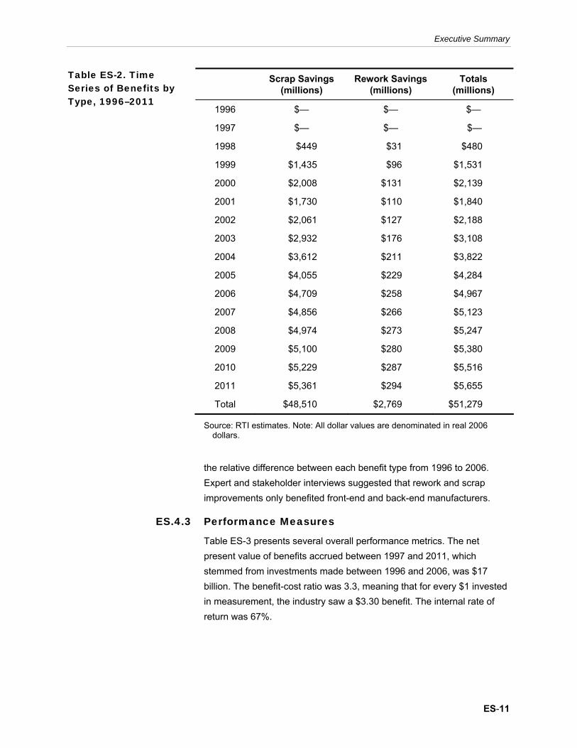
Executive Summary
Table ES-2. Time Scrap Savings Rework Savings Totals Series of Benefits by (millions) (millions) (millions) Type, 1996–2011
1996 $— $— $—
1997 $— $— $—
1998 $449 $31 $480
1999 $1,435 $96 $1,531
2000 $2,008 $131 $2,139
2001 $1,730 $110 $1,840
2002 $2,061 $127 $2,188
2003 $2,932 $176 $3,108
2004 $3,612 $211 $3,822
2005 $4,055 $229 $4,284
2006 $4,709 $258 $4,967
2007 $4,856 $266 $5,123
2008 $4,974 $273 $5,247
2009 $5,100 $280 $5,380
2010 $5,229 $287 $5,516
2011 $5,361 $294 $5,655
Total $48,510 $2,769 $51,279
Source: RTI estimates. Note: All dollar values are denominated in real 2006 dollars.
the relative difference between each benefit type from 1996 to 2006. Expert and stakeholder interviews suggested that rework and scrap improvements only benefited front-end and back-end manufacturers.
ES.4.3 Performance Measures
Table ES-3 presents several overall performance metrics. The net present value of benefits accrued between 1997 and 2011, which stemmed from investments made between 1996 and 2006, was $17 billion. The benefit-cost ratio was 3.3, meaning that for every $1 invested in measurement, the industry saw a $3.30 benefit. The internal rate of return was 67%.
ES-11

Economic Impact of Measurement in the Semiconductor Industry
Table ES-3. Performance Metrics for Investments in Measurement, 1996–2011
Benefits (2006 millions) $51,279
Costs (2006 millions) $12,348
Net benefits (2006 millions) $38,931
NPV of net benefits (2006 millions)a $17,221
Benefit-to-cost ratio 3.3
Internal rate of return 67%
aNPV is discounted to 1996 using a 7% annual discount rate.
Source: RTI estimates.
ES.5 SUMMARY REMARKS It is essential that investment in and collaboration on standards and technology development and on common goal-setting efforts continue. To that end, the industry requires that NIST play a significant role. Past investments in semiconductor measurement standards and technologies have shown themselves to be very beneficial to both the industry and businesses and consumers. Moving forward, firms in the industry will continue their private R&D efforts to shrink feature size, increase wafer size, evaluate and research new materials, and adopt more advanced processing techniques. In the coming years, the industry will continue to work on these four areas, but experts and stakeholders see many areas where problems of measurement exist and where technologies and standards will be needed to prevent technical roadblocks.
In particular, stakeholders and experts mentioned measurement and standards needs in several key technical areas:
• new standards for measuring features lengths at 32 nm
• new techniques for controlling radio-frequency electromagnetic energy and high-frequency magnetic fields
• improved mask measurement standards
• improved chemical and materials standards and processes
• new calibration and standard test methods
• better inoperability standards
ES-12
1 Introduction
The semiconductor industry has long been a driving force behind major advances in computing and electronics. Advances in the speed of processing power have enabled individuals and companies to create, access, and analyze data rapidly, improving individual and business efficiency and developing new markets within the national and global economies.
Between 1996 and 2006, semiconductor manufacturers and semiconductor technology research groups, including the National Institute of Standards and Technology (NIST) and industry consortia, made significant investments in technology infrastructure supporting the industry. The technology infrastructure enables firms to enhance design and production processes that optimize efficiency and effectiveness. Among the infrastructure components in which organizations invested were new measurement systems encompassing equipment, software, and methods. These systems included
• measurement tools and techniques;
• standards for measuring materials, chemicals, and operational or maintenance processes; and
• interoperability standards.
The novel systems they created accelerated the development of less expensive, higher quality semiconductors that enable products as varied as lighting systems and computers. Without these investments, the industry would have otherwise been less efficient, incurring higher defect rates and greater costs, all of which would have been passed along to consumers in terms of higher price, lower quality, or slower processing speed.
1-1
Economic Impact of Measurement in the Semiconductor Industry
The goal of this study, funded by the NIST Program Office, was to quantify the investment made by the semiconductor industry, government, and consortia in the measurement infrastructure between 1996 and 2006 and to compare that estimate with the economic benefits firms accrued as a consequence. This study also analyzed the trends catalyzing a broad-based, public–private strategy for improving the industry’s measurement capabilities and thereby the industry’s competitiveness in the global market.
1.1 THE IMPORTANCE OF MEASUREMENT IN THE SEMICONDUCTOR INDUSTRY The quality and productivity advances experienced by the semiconductor industry over the past few decades would not have been possible without the measurement infrastructure that supports it. Since the 1970s, the semiconductor industry has focused on continually satisfying “Moore’s Law,” the prediction made by Gordon Moore, cofounder of Intel, that the number of transistors per chip in a semiconductor device would double every 2 years. As time progressed, however, achieving that benchmark became more challenging. By the early 1990s, the semiconductor industry was largely focused on making incremental advances in the quality of their products. It soon became readily apparent that the way forward was rooted in exploiting the potential of nanoscale measurement opportunities.
The U.S. government has supported the industry through technology innovation and development assistance since its emergence in the second half of the 20th century. Its continued growth and health remains a federal priority, and federal organizations like NIST sponsor semiconductor research programs. Several industry associations and research groups have been established to guide cross-industry planning and sponsor research into technologies of benefit to the entire industry. Among the groups that currently support standardization and enrichment of the technology infrastructure are
• NIST,
• Semiconductor Manufacturing Technology (SEMATECH),1
1SEMATECH, a consortium of semiconductor manufacturers, formed in 1987 to support the U.S. semiconductor industry’s efforts to remain globally competitive. Funding for SEMATECH originally came from both U.S. government and member companies. The organization has grown significantly and is now funded by and focused on the global semiconductor industry.
1-2

Chapter 1 — Introduction
• Semiconductor Equipment and Materials Institute (SEMI),2
• Semiconductor Industry Association (SIA),3 and
• Semiconductor Research Corporation (SRC).4
These organizations facilitated the collaboration of industry stakeholders through a variety of mechanisms, including “industry roadmaps.” Industry roadmaps are strategy documents that establish consensus views on key issues facing stakeholders. They are often used to articulate systemic issues in an industry and set a course for achieving industry-wide objectives. Industry roadmaps advocated developing the standards and measurement technologies needed to maintain Moore’s Law.
The first National Technology Roadmap for Semiconductors (NTRS) was developed in 1992 and was updated twice over the next 5 years. Supported primarily by SIA, NIST, and SEMATECH, the NTRS focused on developing measurement technologies and standards that could be leveraged by the entire U.S. semiconductor industry. The effort became more global in 1997, taking on the name International Technology Roadmap for Semiconductors (ITRS), and began to develop roadmaps every 2 years with an update in the intervening years.
Advances in measurement technology are often credited with helping the industry keep up with Moore’s Law between 1996 and 2006, during which time the number of possible transistors per logic chip increased from 3.1 million in 1994 to 1.7 billion in 2005 (SIA, 2005). Many factors have helped the industry realize such achievements, most notably the use of significant improvements in data processing and analysis capabilities. However, without the strategic work of ITRS collaborators and, more specifically, the standards and measurement investments made by NIST, consortia, universities, and industry stakeholders, this achievement would not have been possible.
1.2 PROJECT SCOPE AND GOALS The NIST Program Office sponsored this research for two reasons. As a purely retrospective investment analysis, NIST is interested in the impact that advances in measurement infratechnologies, generic technologies,
2SEMI was originally formed in 1970 as a trade association for the semiconductor equipment market. Since the mid-1970s, it has played a vital role in developing standards used by the entire semiconductor industry.
3SIA is the principal U.S. manufacturers’ trade association for the semiconductor industry. It was founded in 1977 and has 95 members.
4SRC is a global research consortium founded in 1982 that administers a broad university research program to advance semiconductor technologies.
1-3

Economic Impact of Measurement in the Semiconductor Industry
and associated standards have had on the semiconductor industry.5
Although many of its research programs support semiconductor research, design, and production activities, two key NIST programs are devoted to semiconductors:
• Semiconductor Electronics Division (SED). SED supports government, industry, and academic stakeholders by providing essential technology infrastructure, including measurement, physical standards, supporting data and technology, and generic technology. The division also communicates research results and practices to the industry.
• Office of Microelectronics Programs (OMP). OMP offers expert support to NIST and the industry on current and future measurement needs of the industry; their expertise includes (but is not limited to) the following types of measurement: lithography, critical dimension and overlay, front-end processing, interconnect and packaging, and back-end processing. They facilitate interactions within the industry and provide expert support to manufacturers.
This analysis is also important for both NIST and companies throughout the industry as part of their joint strategic planning process. Analyzing past impacts and future needs can help the industry and supporting bodies such as NIST focus attention and investment dollars on measurement issues projected to be most significant and to show substantive returns from past investments.
This section begins by defining and distinguishing between two terms that are critical to conceptualizing the study’s scope and major goals: “measurement” and “metrology.”
1.2.1 Measurement versus Metrology
This study focused on the impact of investments in measurement technologies and standards implemented in the semiconductor industry between 1996 and 2006. In the industry, the term "metrology" is often used to describe the adoption and use of measurement equipment for manufacturing or quality assurance activities. This study uses the slightly broader term of “measurement” to include what the industry calls metrology plus
• software used to automate and simplify design activities (that must be based on precise measurement data),
5See Tassey (2005) for a discussion of generic technologies and infratechnologies that support industry.
1-4

Chapter 1 — Introduction
• standard reference materials (SRMs) used to ensure consistency (and sometimes accuracy) of chemical and materials measurements within and across companies,
• interoperability standards that enable efficient sharing of design and process flow data between equipment and business partners, and
• calibration and testing standards used to certify that equipment and products at each stage have been measured adequately.
“Measurement” in this study, therefore, includes measurement standards and a suite of technologies and tools that enable effective use of those standards.
1.2.2 Important Project Scope Parameters
Two project limitations are important to note. First, the study’s focus was on investment activities and associated benefits within the United States. However, the semiconductor industry is global and most U.S. semiconductor companies have offices, research and development (R&D), and manufacturing facilities outside the United States.6 Every effort was made to ensure that survey and interview participants responded only for their U.S. facilities; however, it is possible that costs and benefits accruing to entities outside the United States were included inadvertently. Expert interviews were similarly focused on U.S. adoption and use of measurement standards and technologies.
Second, this study did not attempt to quantify the impact of investments in measurement on improvements in product quality or subsequent benefits flowing to businesses and consumers who use products with higher quality semiconductors. Quantifying consumer benefits would have required resources far beyond those allocated to this study; therefore, consumer benefits were excluded from the analysis.
1.2.3 Key Study Objectives
This study assessed the net benefits of improvements to the measurement infrastructure supporting the semiconductor industry between 1996 and 2006. To this end, it focuses on the incremental adoption of and associated investments in measurement technologies
6For example, Intel’s “Copy Exactly” strategy involves the development of processes in one region (e.g., the United States) and the simultaneous introduction of the lessons learned in the United States, Ireland, and Israel (see http://news.com.com/Intel+to+ expand+Irish+manufacturing+facilities/2100-1006_3-5216309.html).
1-5

Economic Impact of Measurement in the Semiconductor Industry
and standards and the economic impact these developments have had on the industry.7 Specifically, the main objectives of this study were to
• describe and assess the economic roles of the technology infrastructure that supports the semiconductor industry,
• quantify industry investments in measurement-related technologies and systems between 1996 and 2006, and
• quantify the collective benefit that advances in measurement between 1996 and 2006 have had on the semiconductor industry in terms of growth and competitiveness.
In addition, this study aimed to gather information on the future trends and needs of the industry and to propose potential roles for NIST to support the industry effectively.
1.3 REPORT ORGANIZATION The remainder of this report is organized as follows:
• Chapter 2 discusses the process flow of the semiconductor industry and presents a taxonomy of major stakeholder groups and measurement categories.
• Chapter 3 presents a detailed analysis of the major advances in measurement technologies and standards between 1996 and 2006. A more detailed version of this chapter with an engineering discussion of technical advances is included as Appendix A.
• Chapter 4 explains the methodology used to estimate the adoption of new measurement technologies and standards and quantify costs and benefits.
• Chapter 5 presents the analysis results for investments made in measurement infrastructure between 1996 and 2006. It also includes survey data on the extent to which new measurement technologies were adopted during that period.
• Chapter 6 presents the analysis results for economic benefits.
• Chapter 7 concludes this report with a summary of findings and recommendations for future research and opportunities for NIST.
7Note that all references to “measurement expenditures” in this report refer to expenditures on new technologies and standards implemented between 1996 and 2006, as opposed to fixed and variable costs on older generation technology and standards.
1-6
2Overview of the Semiconductor
Industry
This chapter provides an overview of the role of semiconductors, or chips in the industry vernacular, and describes the basic steps in the semiconductor manufacturing process. In a world of devices reliant on electricity, semiconductors are the workhorses that take electric voltage and engender device function. Semiconductors are the tiny devices, usually made of silicon and densely packed with transistors, that relay, switch, or amplify electricity and permit electrical devices to function as intended.
Producing semiconductors involves converting a variety of materials (e.g., gases, liquids, and metals) into either a single discrete device, with a single function, or an “integrated circuit,” which combines many devices into one semiconductor device. Integrated circuits, or ICs, include microprocessors, which control everyday products such as microwave ovens and more advanced products such as cellular phones and computers. The steps involved in manufacturing a semiconductor are complex, and the technologies involved change rapidly to enable the development of more advanced products.
Understanding the measurement improvements made between 1996 and 2006 first requires an introduction to key terminology, an understanding of how semiconductors are made, and an overview of why measurement is critical in an industry in which tolerances are denominated in very small measurements (e.g., nanometers). This chapter also identifies the major stakeholder groups in the industry and provides a taxonomy for understanding the major categories of measurement technologies and standards. Chapter 3 delves into the measurement advances for which development costs were quantified and economic benefits were estimated.
2-1
Economic Impact of Measurement in the Semiconductor Industry
2.1 ROLE OF SEMICONDUCTORS The influence of the semiconductor industry increased dramatically between 1996 and 2006. New, ever more powerful semiconductor devices catalyzed incredible growth in the computer, consumer electronics, and Internet industries. Consumers benefited from the introduction of novel electronic products as diverse as mp3 players, advanced health care technologies, digital imaging technologies, new means (i.e., the Internet) by which to search for and buy goods, and more readily available ways to communicate with others. Businesses benefited from new data collection and analysis capabilities that enabled robust productivity analysis, error analysis, and market segmentation and forecasting. Advanced communications tools, Internet technologies, and mobile computing power enable employees to work more efficiently.8
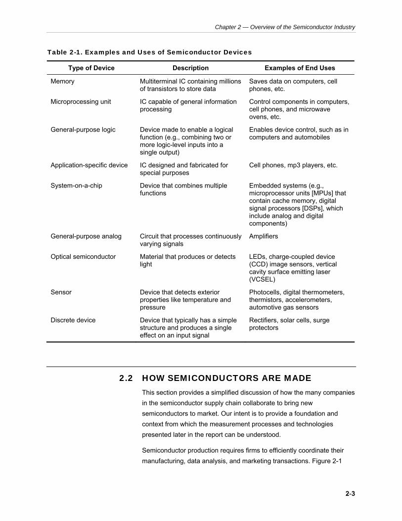
Semiconductors are most often thought of as being intended for data processing applications, such as microprocessors and memory, because the largest and most well-known American manufacturers, Intel and Texas Instruments, dominate that market. But semiconductors can be found in irons and alarm clocks, radios, and automobile taillights. As devices become more sophisticated, the semiconductors enabling them become more sophisticated as well. The same devices that once enabled computers are now found in cell phones, digital cameras, and video game consoles. Table 2-1 provides an overview of different types of semiconductor devices and their common applications.
Worldwide sales of semiconductor devices increased from $132 billion in 1996 to $248 billion in 2006 (SIA, 2006). And between 2007 and 2010, the semiconductor industry is projected to grow almost 8% annually (Gordon, 2006).
Memory and microprocessors account for almost half of all semiconductor sales (42%), application-specific devices (e.g., for mobile phones and digital cameras) account for 33%, and the remaining 25% is a mixture of device types. The research group Gartner projects that by 2010 application-specific products will account for more than half of total industry revenue (Rieppo, 2005).
8Several recent studies provide empirical evidence that significant positive returns to IT investment can be consistently achieved in the manufacturing and service sectors (Bharadwaj, Bharadwaj, and Konsynski, 1999; Bresnahan, Brynjolfsson, and Hitt, 2002; Brynjolfsson and Hitt, 1996; Dewan and Min, 1997; and Lichtenberg, 1995).
2-2
Chapter 2 — Overview of the Semiconductor Industry
Table 2-1. Examples and Uses of Semiconductor Devices
Type of Device Description Examples of End Uses
Memory Multiterminal IC containing millions of transistors to store data
Saves data on computers, cell phones, etc.
Microprocessing unit IC capable of general information processing
Control components in computers, cell phones, and microwave ovens, etc.
General-purpose logic Device made to enable a logical function (e.g., combining two or more logic-level inputs into a single output)
Enables device control, such as in computers and automobiles
Application-specific device IC designed and fabricated for special purposes
Cell phones, mp3 players, etc.
System-on-a-chip Device that combines multiple functions
Embedded systems (e.g., microprocessor units [MPUs] that contain cache memory, digital signal processors [DSPs], which include analog and digital components)
General-purpose analog Circuit that processes continuously varying signals
Amplifiers
Optical semiconductor Material that produces or detects light
LEDs, charge-coupled device (CCD) image sensors, vertical cavity surface emitting laser (VCSEL)
Sensor Device that detects exterior properties like temperature and pressure
Photocells, digital thermometers, thermistors, accelerometers, automotive gas sensors
Discrete device Device that typically has a simple structure and produces a single effect on an input signal
Rectifiers, solar cells, surge protectors
2.2 HOW SEMICONDUCTORS ARE MADE This section provides a simplified discussion of how the many companies in the semiconductor supply chain collaborate to bring new semiconductors to market. Our intent is to provide a foundation and context from which the measurement processes and technologies presented later in the report can be understood.
Semiconductor production requires firms to efficiently coordinate their manufacturing, data analysis, and marketing transactions. Figure 2-1
2-3

Economic Impact of Measurement in the Semiconductor Industry
Figure 2-1. Semiconductor Industry Supply Chain and Major Process Flows
Basic and applied R&D organizations
All industry stakeholder
groups
IC designers Front-end and
back-end processing firms
Chemical/ materials suppliers
Equipment (production and
metrology ) suppliers
Software suppliers
Semiconductor devices are sold
to electronics manufacturers (e.g., computer manufacturers)
RESEARCH AND DEVELOPMENT
ACTIVITIES
PRODUCTION INPUT
CREATION
PRODUCTION ACTIVITIES
SALES ACTIVITIES
= Data and information flows
= Software flows
= Materials and product flows
provides an overview of industry stakeholder collaboration through three process flows: (1) data and information, (2) software products, and (3) physical products (i.e., raw chemicals and materials and final products).
First, R&D organizations and staff at all stakeholder groups work on developing the technologies, standards, and technical processes necessary to build and produce a new type of semiconductor device. This information feeds into the knowledge base of both suppliers and device producers.
2-4

Chapter 2 — Overview of the Semiconductor Industry
Suppliers use this information to
• produce the necessary equipment to create the device as well as the chemicals and materials,
• develop the necessary software packages to enable chip design and analysis of production facility operations,
• design the exact physical characteristics of the new device and how it will be produced, and
• ensure the necessary chemicals and materials are used and are provided to the correct specificity.
Beginning with raw materials and a design, manufacturers invest in the necessary production equipment and software to turn their raw materials and designs into chips. Production is extraordinarily capital intensive because humans cannot manually produce semiconductors at the scale or precision demanded. Instead, robots and advanced photolithography technologies are combined in an automated environment monitored in real time by computing systems overseen by technicians. These chips are then turned over to test and assembly firms to create a final product that is then put into electronic products for sale to consumers or businesses.
Semiconductor production occurs in two stages. First, a manufacturer uses the designs provided to develop the necessary production line, including the production and measurement equipment. A multiple-step sequence of photographic and chemical processing tasks is followed to create electronic circuits on a wafer—a round flat slice of pure semiconducting material, most commonly silicon. In the most advanced manufacturing or fabrication plants (often referred to as “fabs”), more than a billion transistors are created on one wafer. The wafer fabrication process is the most expensive and complex part of developing a semiconductor device (see the textbox on the next page for more detail on this process).
These chips are then sent to the second stage called “package and testing” (or “assembly and testing”). The properties of the circuits on each wafer are tested, and then it is cut into individual “chips.” Each chip is packaged, usually in plastic or ceramic components, by connecting the chip to metal (usually gold) pins on the package so that it can be connected to the product in which it will be used.
This two-stage manufacturing process, beginning with the wafer fabrication and ending with a packaged chip ready to be shipped, takes
2-5
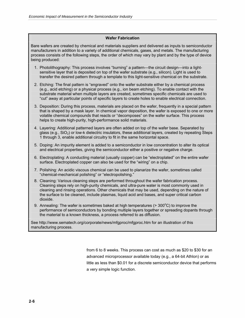
Wafer Fabrication
Economic Impact of Measurement in the Semiconductor Industry
Bare wafers are created by chemical and materials suppliers and delivered as inputs to semiconductor manufacturers in addition to a variety of additional chemicals, gases, and metals. The manufacturing process consists of the following steps, the order of which may vary by plant and by the type of device being produced:
1. Photolithography: This process involves “burning” a pattern—the circuit design—into a light-sensitive layer that is deposited on top of the wafer substrate (e.g., silicon). Light is used to transfer the desired pattern through a template to this light-sensitive chemical on the substrate.
2. Etching: The final pattern is “engraved” onto the wafer substrate either by a chemical process (e.g., acid etching) or a physical process (e.g., ion beam etching). To enable contact with the substrate material when multiple layers are created, sometimes specific chemicals are used to “cut” away at particular points of specific layers to create holes to enable electrical connection.
3. Deposition: During this process, materials are placed on the wafer, frequently in a special pattern that is shaped by a mask layer. In chemical vapor deposition, the wafer is exposed to one or more volatile chemical compounds that reacts or “decomposes” on the wafer surface. This process helps to create high-purity, high-performance solid materials.
4. Layering: Additional patterned layers are often added on top of the wafer base. Separated by glass (e.g., SiO2) or low-k dielectric insulators, these additional layers, created by repeating Steps 1 through 3, enable additional circuitry to fit in the same horizontal space.
5. Doping: An impurity element is added to a semiconductor in low concentration to alter its optical and electrical properties, giving the semiconductor either a positive or negative charge.
6. Electroplating: A conducting material (usually copper) can be “electroplated” on the entire wafer surface. Electroplated copper can also be used for the “wiring” on a chip.
7. Polishing: An acidic viscous chemical can be used to planarize the wafer, sometimes called “chemical-mechanical polishing” or “electropolishing.”
8. Cleaning: Various cleaning steps are performed throughout the wafer fabrication process. Cleaning steps rely on high-purity chemicals, and ultra-pure water is most commonly used in cleaning and rinsing operations. Other chemicals that may be used, depending on the nature of the surface to be cleaned, include plasmas, liquid acid and bases, and super critical carbon dioxide.
9. Annealing: The wafer is sometimes baked at high temperatures (> 300oC) to improve the performance of semiconductors by bonding multiple layers together or spreading dopants through the material to a known thickness, a process referred to as diffusion.
See http://www.sematech.org/corporate/news/mfgproc/mfgproc.htm for an illustration of this manufacturing process.
from 6 to 8 weeks. This process can cost as much as $20 to $30 for an advanced microprocessor available today (e.g., a 64-bit Athlon) or as little as less than $0.01 for a discrete semiconductor device that performs a very simple logic function.
2-6

Chapter 2 — Overview of the Semiconductor Industry
2.3 STAKEHOLDERS IN THE SEMICONDUCTOR INDUSTRY Semiconductor manufacturing involves a wide variety of organizations with technical expertise ranging from basic chemistry and software development to sensors and process control systems. For the purpose of this study, we define the semiconductor supply chain in terms of the following stakeholder groups:
• basic and applied R&D organizations
• equipment suppliers
• software suppliers
• product designers (referred to as “IC designers” in this study since the vast majority of designers create IC designs)
• chemical and materials suppliers
• front-end processing facilities (wafer fabrication facilities)
• back-end processing facilities (packaging, assembly, and test plants)
As shown in Figure 2-1, the flow of information and material products begins with public and private R&D organizations. This group is composed of public institutions, universities, private laboratories (usually owned by device manufacturers), and public–private partnerships such as NIST, SEMATECH, SEMI, SIA, and SRC. These organizations conduct basic research and help determine industry standards that improve the efficiency of the semiconductor supply chain, in particular the manufacturing process. The knowledge and skills gained from basic research flow to suppliers of measurement equipment and software—the primary producers of measurement products.
Equipment and software suppliers develop the tools necessary for the rest of the supply chain to operate. Using technologies developed by R&D organizations and within the supply chain, equipment suppliers produce both ex situ (off the production line) equipment and in situ (in process). Software suppliers develop new applications that help streamline the development of chip designs and integrate new technological developments into these applications as they are developed. These two groups help support all subsequent stakeholder groups.
The next flow of information and measurement hardware and software is through IC designers. Many IC designers are part of manufacturing firms (e.g., Intel and Advanced Micro Devices have “in house” IC design
2-7
Economic Impact of Measurement in the Semiconductor Industry
divisions), although some operate as “fabless” firms that outsource the manufacturing of the chips they design and sell. Measurement improvements enable this group to design higher quality chips with fewer defects at faster speeds; however, these designers must also spend labor resources on measurement-related R&D and must incur expenditures for installing equipment and software. IC design firms then give specifications for production inputs to chemical and materials suppliers. This group of raw and processed materials suppliers likely incurs some cost for installing measurement products and R&D but receives both productivity and quality benefits.
Chemical and materials suppliers, design firms, and equipment and software suppliers together provide the inputs to front-end and back-end processing firms. These firms are the major consumers of all measurement-related capital and information in the semiconductor supply chain. These two groups expend labor resources for R&D and installation of measurement equipment and software that they must purchase; however, they receive benefits of both increased productivity and product quality. Of note, some processing firms outsource certain measurement analysis activities to independent analytical firms; thus, these firms are part of the supply chain, incurring R&D and installation expenditures, and derive benefits from measurement improvements with increased productivity.
The U.S. supply chain stakeholder revenues are listed in Table 2-2 for 1996 and 2006. Front-end processing firms represent more than 70% of the industry with 2006 revenues of approximately $88 billion, while equipment manufacturers are the second largest group with around 15% of the industry or $19 billion in 2006 revenues.
2.4 MEASUREMENT CATEGORIES: A TAXONOMY Each of the main semiconductor stakeholders relies on a suite of interrelated measurement capabilities. This study grouped measurement improvements in the semiconductor industry into six major categories:
• product design tools
• software standards and interoperability
• calibration and standard test methods
• ex situ process control techniques
• in situ process control techniques
• quality assurance (QA)
2-8

Chapter 2 — Overview of the Semiconductor Industry
Table 2-2. U.S. Semiconductor Revenue by Stakeholder Group, 1996 and 2006
1996 Revenue 2006 Revenue Stakeholder Group (millions) (millions) % Change
IC design firms $3,177 $3,033 −4.8%
Chemical/materials suppliers $1,338 $1,408 5.0%
Equipment suppliers $17,853 $18,787 5.0%
Front-end processing firms $85,000 $88,145 3.6%
Back-end processing firms $7,566 $7,962 5.0%
Software suppliers $3,872 $4,075 5.0%
Source: RTI estimates based on U.S. Census Manufacturing Industry Series data, Gartner, and conversations with industry analysts. Note: All estimates are in nominal dollars.
Product design tools include a variety of software applications that are used by semiconductor device and IC design firms to quickly and accurately design the structure and characteristics of a new device type. This category of software applications, often referred to as electronic design for automation (EDA) tools, includes software applications used to (1) develop the design of a device, (2) help to prevent and correct for production errors, (3) run simulations of device and process functionality, and (4) manage the product life cycle. Without these tools, the complex devices (or chips) produced between 1996 and 2006 could not have been designed; creating such designs by hand would have been extremely time consuming and error prone.
Software standards and interoperability encompasses the use of standard languages by which software applications can communicate more easily with each other as well as with hardware-based languages. Two primary types are verification languages and data formats. Verification languages enable the simulation of circuit designs while avoiding the cost of building and testing physical prototypes of early-stage designs. Data formats include those for graphics used to specify models of the surface characteristics for components manufactured in the production process. Although the underlying simulation capabilities could have been achieved in the absence of these standards, the resulting bottlenecks to effective communication would likely have delayed or perhaps precluded the development of new devices.
Calibration and standard test methods increase the precision and accuracy of operations, In addition to reducing rework and scrap costs
2-9
Economic Impact of Measurement in the Semiconductor Industry
associated with less accurate measurement, calibration and standard test methods provide a basis for measurements taken anywhere in the world to be compared with confidence. This is critical to ensuring that parts manufactured in one part of the world meet the same performance specifications globally.
Ex situ process control technologies can essentially be defined as measurements taken “on wafer” but not on the production line. Essentially, ex situ equipment is used to take measurements away from the processing equipment, often in a centralized location. Although the ex situ process control area is very broad, the characteristics and trends can be grouped into measuring the two-dimensional components of a wafer (often called critical dimension [CD] measurements) and measuring the three-dimensional components of the wafer (often referred to in this context as a “thin film”). Characteristics such as thickness, chemical composition, and structure are essential to the operation of a semiconductor device as designed.
In situ process control technology allows real-time, within-process control. As opposed to ex situ technology, which is housed in separate equipment and requires that semiconductor components be transported to their location, in situ measurements can be taken much more quickly and require less coordination. By taking measurements in “real time,” adjustments can be made more quickly (before more wafers have continued through production). In situ process control directly saves time and money when high rates of production are involved.
QA is defined in this study as the methods manufacturers use to ensure that their finished products meet their customers’ specifications. The intent of QA is to certify a product or material prior to providing it to the next stage in the value chain as well as to test incoming materials. Changes in QA techniques result from new technology developments that allow earlier assessments of process parameters and faster and more effective process control responses.
2-10

Advances in Measurement in the Semiconductor3 Industry
This study grouped measurement improvements in the semiconductor industry into six major categories:
• product design tools
• software standards and interoperability
• calibration and standard test methods
• ex situ process control techniques
• in situ process control techniques
• quality assurance
Many of these measurement categories are based on industry goals developed as part of U.S. and international technology. However, the categories included in this study were broadened to accommodate additional technology areas.
Figure 3-1 provides several examples for each of the six categories listed above, as well as an overview of how the categories relate to industry stakeholder groups. The figure focuses on the design and production process for a semiconductor chip; thus, it does not include supporting organizations such as consortia or other groups involved in process R&D. However, industry consortia and research organizations play an important role in developing the measurement infrastructure. Their investments are discussed in the quantitative analysis outlined in Chapter 4 and quantified in Chapter 5.
The lines between some infrastructure categories blur. As Figure 3-1 shows, with the exception of IC design, stakeholder groups rely on a wide range of measurement-related infratechnologies. For example, front-end processing firms use software standards, physical standards,
3-1

Figure 3-1. Overview of the Roles of Measurement in Semiconductor Design and Production
Supply Chain Use of Measurement-Related Infratechnologies and Processes
Integrated Circuit (IC) Design
Product Design Tools
• Electronic design automation
• Simulation software
Software Standards and Interoperability
• Software and standards for passing specifications from
Calibration and Standard Test
Methods
• Measurement
Chemical, Materials, and
fabrication facilities design labs to mask
• Standard reference materials
standards
Ex Situ Process Control Technology
In Situ Process Control Technology
Quality Assurance
Equipment Supply • ASTM and other standard test • Water and gas control
• Wafer bow and smoothness
• Chemical processing • Wafer manufacturing • Mask manufacturing • Equipment, software
manufacturing
methods
• SEMI standards for wafer dimension and structure
•
methods (e.g., optical microscopy and particle counters)
Mask and wafer CD measurement (e.g.,
•
levels)
• Gas and liquids purity
• Metal target purity
Wafer properties (e.g., purity and dopant
Front-End Processing
• Layering • Photolithography • Etching, striping • Doping/ion implantation
• Standard transfer mechanisms
• Standard information exchange formats (IGES, DXF, GDS II)
• Advanced process control (APC)
standards
• SRMs for wafers, compound semiconductors, and epitaxial layers
• SRMs for implantation
• Linear distance and SEM)
• Thermal/thin film metrology—structure, composition, and stress
optical microscopy • Process vacuum control (gages, residual gas analyzers)
• Monitoring of processing parameters (e.g., temperature,
• Carrier mobility and lifetime
• Particle monitors and counters
• Electrostatic discharge monitoring
• Electrical test
• Metal interconnects • CMP (polishing)
standards • Mass flow controllers calibration
• Sampling algorithms
• Technologies used in automation, robotics, and sample handling
• ASTM and/or other
• Overlay measurement tools
• Doping profile measurement tools
• Patterned wafer inspection, including defect analysis and electrical
pressure)
• Deposition monitoring and endpoint detection
Back-End Processing
• Testing • Assembly • Packaging
• Factory database management
• Integrated production and scheduling (IPS)
methods
• Statistical metrology
• Sampling algorithms
• Probe contact variations
standard test characterization • End-of-line electrical test
• Burn-in and accelerated life tests
Note: This figure focuses directly on the design and production process for a semiconductor chip; thus, it does not include supporting organizations such as consortia or other groups involved in process R&D. However, these additional stakeholders play an important role in developing measurement infrastructure.
Econom
ic Impact of M
easurement in the S
emiconductor Industry
3-2
Chapter 3 — Advances in Measurement in the Semiconductor Industry
ex situ and in situ process control infratechnologies, and QA infratechnologies.
This chapter begins with a discussion of the need for new measurement technologies and standards in the early 1990s and describes several important industry roadmaps established by industry consortia to improve best practices in the industry. Next, the chapter discusses the origins of key infratechnology improvements in each measurement category for which costs and benefits were analyzed. A more detailed technical discussion of process improvements is included as Appendix A.
3.1 A DECADE OF CHANGES IN MEASUREMENT In the mid-1990s, two factors combined to catalyze cross-industry collaborative efforts to improve measurement: technical barriers that challenged Moore’s Law and competitive pressures from foreign producers and electronics manufacturers. The semiconductor industry relied on its long-standing history of collaboration to take advantage of economies of scale in research spending on generic technologies. NIST and industry associations provided fundamental measurement and semiconductor research support that made it possible to break through technical barriers.
3.1.1 The Impetus for Increased Measurement Investment
Rapid gains in manufacturing technology converged with competitive and cost pressures—from foreign producers and consumers—to compel the semiconductor industry to implement highly sophisticated measurement strategies to achieve gains in productivity, quality, and profits. Customers were demanding greater processing power and speed, shorter development times, and lower costs.
Technology Changes
As shown in Figure 3-2, in general, three types of changes in the production process pushed the industry to invest in measurement:
• new production materials were being introduced
• wafer sizes were increasing
• the distance between lines of memory (dynamic random access memory, or DRAM9) chips was decreasing
9Using DRAM as a point of reference is the common way to discuss and measure the increasingly smaller sizes of device components; however, SRAM (static random access memory), Flash memory, or ROM (read-only memory) all use smaller components as well.
3-3
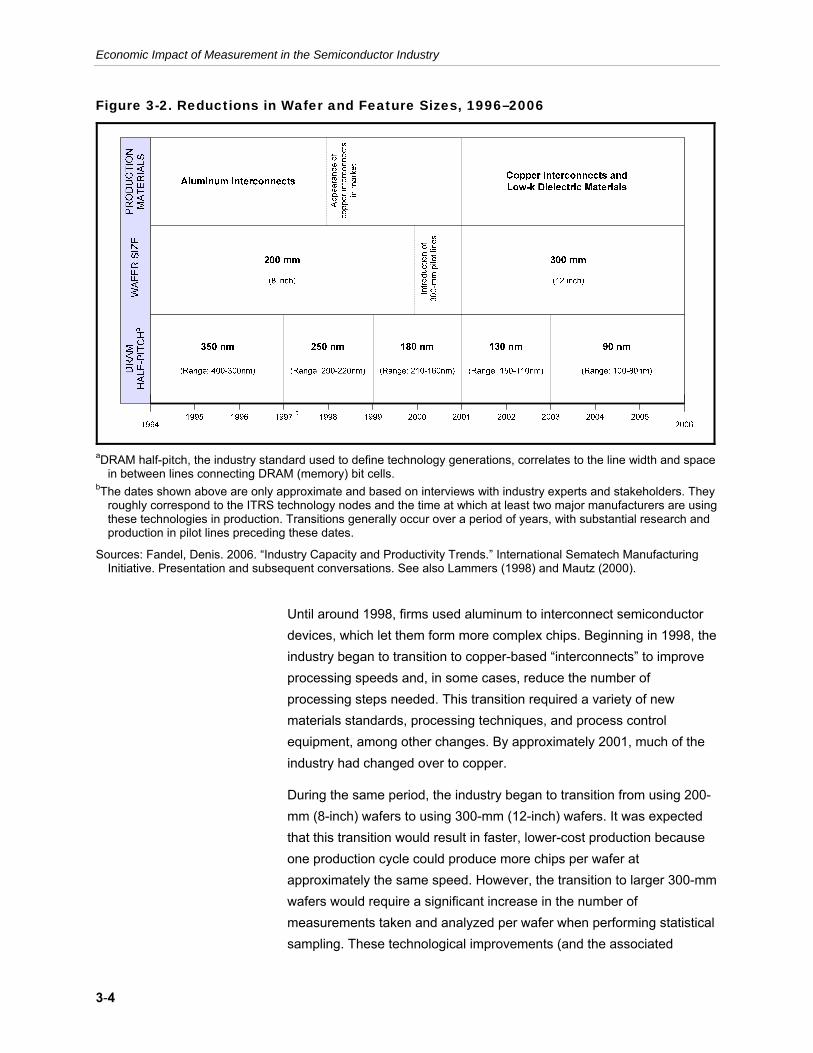
Economic Impact of Measurement in the Semiconductor Industry
Figure 3-2. Reductions in Wafer and Feature Sizes, 1996–2006
aDRAM half-pitch, the industry standard used to define technology generations, correlates to the line width and space in between lines connecting DRAM (memory) bit cells.
bThe dates shown above are only approximate and based on interviews with industry experts and stakeholders. They roughly correspond to the ITRS technology nodes and the time at which at least two major manufacturers are using these technologies in production. Transitions generally occur over a period of years, with substantial research and production in pilot lines preceding these dates.
Sources: Fandel, Denis. 2006. “Industry Capacity and Productivity Trends.” International Sematech Manufacturing Initiative. Presentation and subsequent conversations. See also Lammers (1998) and Mautz (2000).
Until around 1998, firms used aluminum to interconnect semiconductor devices, which let them form more complex chips. Beginning in 1998, the industry began to transition to copper-based “interconnects” to improve processing speeds and, in some cases, reduce the number of processing steps needed. This transition required a variety of new materials standards, processing techniques, and process control equipment, among other changes. By approximately 2001, much of the industry had changed over to copper.
During the same period, the industry began to transition from using 200-mm (8-inch) wafers to using 300-mm (12-inch) wafers. It was expected that this transition would result in faster, lower-cost production because one production cycle could produce more chips per wafer at approximately the same speed. However, the transition to larger 300-mm wafers would require a significant increase in the number of measurements taken and analyzed per wafer when performing statistical sampling. These technological improvements (and the associated
3-4

Chapter 3 — Advances in Measurement in the Semiconductor Industry
product and productivity improvements) would not have been possible without the supporting advances in measurement technology.
Several levels of changes have occurred in what is known as “DRAM half-pitch,” which refers to the space between metal lines of DRAM “bits.” Essentially, moving to a smaller half-pitch means that more memory can fit into a given area on a chip. The industry often uses this metric to describe general reductions in “feature size”—the space between semiconductor components in a device. Decreasing feature sizes meant that defects and structural variances would become significant even at the nanometer level, requiring increased measurement capabilities and greater control of processing parameters.
Only the most advanced semiconductor devices changed to larger wafer sizes, smaller feature sizes, and new production materials. Therefore, increases in measurement technologies were not needed for the production of all types of semiconductor devices. Table 3-1 shows the relative importance of investments in measurement technologies between 1996 and 2006 for each type of semiconductor device. Gartner researchers and other industry experts suggest that memory and microprocessors have required the most significant advances in measurement technologies and processes compared with other types of semiconductor devices.
Between 1996 and 2006, feature sizes shrunk four times: from 350 nm to 90 nm. Today, most of the industry is using 90-nm technologies, but manufacturers of cutting edge microprocessors and memory are now using 65-nm technologies and some companies are beginning to use 45-nm technologies.
Production Cost Reduction
Reducing the cost of production was another motivation for companies to invest in new measurement technologies. The industry increased operating efficiency, while increasing the performance of and decreasing the cost of semiconductors for its customers. One estimate noted an 18% decrease per year in the cost per transistor (Jorgenson and Wessner, 2004). Increased automation has also been a significant industry trend helping to reduce variable (maintenance and operational) labor costs.
3-5
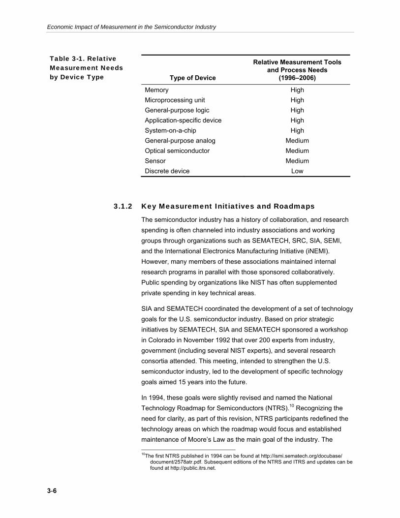
Economic Impact of Measurement in the Semiconductor Industry
Table 3-1. Relative Measurement Needs by Device Type Type of Device
Relative Measurement Tools and Process Needs
(1996–2006)
Memory High Microprocessing unit High General-purpose logic High Application-specific device High System-on-a-chip High General-purpose analog Medium Optical semiconductor Medium Sensor Medium Discrete device Low
3.1.2 Key Measurement Initiatives and Roadmaps
The semiconductor industry has a history of collaboration, and research spending is often channeled into industry associations and working groups through organizations such as SEMATECH, SRC, SIA, SEMI, and the International Electronics Manufacturing Initiative (iNEMI). However, many members of these associations maintained internal research programs in parallel with those sponsored collaboratively. Public spending by organizations like NIST has often supplemented private spending in key technical areas.
SIA and SEMATECH coordinated the development of a set of technology goals for the U.S. semiconductor industry. Based on prior strategic initiatives by SEMATECH, SIA and SEMATECH sponsored a workshop in Colorado in November 1992 that over 200 experts from industry, government (including several NIST experts), and several research consortia attended. This meeting, intended to strengthen the U.S. semiconductor industry, led to the development of specific technology goals aimed 15 years into the future.
In 1994, these goals were slightly revised and named the National Technology Roadmap for Semiconductors (NTRS).10 Recognizing the need for clarity, as part of this revision, NTRS participants redefined the technology areas on which the roadmap would focus and established maintenance of Moore’s Law as the main goal of the industry. The
10The first NTRS published in 1994 can be found at http://ismi.sematech.org/docubase/ document/2578atr.pdf. Subsequent editions of the NTRS and ITRS and updates can be found at http://public.itrs.net.
3-6

Chapter 3 — Advances in Measurement in the Semiconductor Industry
technology areas of this original roadmap (and subsequent version) were as follows:
• sensors and methodology for in situ process control
• process integration, devices, and structures
• materials and bulk processes
• lithography
• interconnect
• factory integration
• measurement capability
In 1998, the roadmap became international when U.S.-based groups partnered with semiconductor organizations in Europe, Japan, Korea, and Taiwan and renamed the initiative the International Technology Roadmap for Semiconductors (ITRS). This international effort has developed a new, revised roadmap for the industry every 2 years since 1999.11
Semiconductor firms, industry consortia, and government agencies around the world have continued to work together to develop explicit technical specifications necessary to keep the industry moving forward. Despite the competition that exists within the companies in this industry, extensive collaboration has led to the development of new infratechnologies and standards that are now the focus of this study.
The following sections detail the major changes in the semiconductor industry from 1996 to 2006, by measurement category.
3.2 PRODUCT DESIGN TOOLS Design tools have a complex interrelationship with measurement equipment. Among the techniques firms use are simulations that eliminate the requirement to build and test physical prototypes. These simulations are enabled by advanced measurement techniques. The integration between semiconductor design and manufacturing processes is deepening, and product design tools are now tightly coupled with the full suite of measurement tools.
Between 1996 and 2006, the most critical product design tool contributions have come from the emergence of electronic design for automation tools, a category of software tools used to design and
11For further information on the history of technology roadmaps in the semiconductor industry, see Spence and Doering, (2005).
3-7
Economic Impact of Measurement in the Semiconductor Industry
3.2.1
3.2.2
produce semiconductors. Although derived from systems developed in the early 1980s, EDA came into its own in the late 1990s when device complexity and cost forced the elimination of initial design prototyping to verify that they met specifications. Based on the acquisition and related integration of other specialized tools by the major EDA firms over time, today the term "EDA tool" has essentially come to be synonymous with product design tools.
Four subcategories of semiconductor design tools are included in the scope of this study:
• system design tools
• design for manufacturability (DFM)
• device and process simulation
• product life-cycle management (PLM)
System Design Tools
System design tools include the initial specification, functional verification, and optimization of a semiconductor device. Virtual design and simulation systems were included in systems developed in the 1990s, permitting implementation of chip-design technologies at the 130-nm level. Prior design systems lacked complete simulation capabilities and required time-consuming and numerous costly design-build-test cycles that made it impossible to progress beyond 180-nm technology.
Functional verification—the assurance that a design performs as intended—is a key step that involves using standardized methods to conduct logical simulation, where software simulation models test the candidate product’s functionality, and hardware emulation is used to verify this functionality. Critical to this capability were accelerated simulation capabilities that resulted from the availability of significantly improved platform power. Enhancements included parallel processing capabilities (i.e., two or more processors powering a system) that allowed many system design functions to be performed in parallel rather than as a series of discrete steps run in batch mode.
Design for Manufacturability
DFM is the extension of lithography to extremely small “subwavelength” dimensions using optical proximity correction (OPC) and reticle-enhancement technology (RET) to account and correct for process distortions. These capabilities were critical to enabling the development of 130-nm-based devices through the use of optical photolithography
3-8
Chapter 3 — Advances in Measurement in the Semiconductor Industry
rather than having to adopt a radically new generation of machines that could no longer use traditional optical focusing techniques.
Although the application of OPC and RET techniques to photolithography provided the most substantial benefits between 1996 and 2006, DFM techniques are the basis for compensating for any known distortions in the manufacturing process, including etching, planarization, and deposition. As semiconductor dimensions shrink, DFM becomes increasingly important to compensate for both tool and physical variations at the chip level.
3.2.3 Device and Process Simulation
Device and process simulation tools simulate physics, optics, and thermal characteristics. This category of design tools is expanding to include a broad range of additional capabilities to manage analog and radio frequency requirements necessary for “systems on a chip” (SoC) devices. Also included are a variety of process simulations that, whether formally integrated or not, have an impact on the design process. In addition, general-purpose design and process simulation tools are becoming increasingly important as semiconductor design focuses more on software than hardware. These stand-alone tools are not currently included in EDA software packages.
3.2.4 Product Life-Cycle Management
Although not currently incorporated into major EDA systems packages, PLM systems are beginning to play a role in tying together the diverse semiconductor supply chain. Their capabilities complement the use of standards, interoperability, and the sharing of information between design and manufacturing—all increasingly significant as the industry moves forward.
3.3 SOFTWARE STANDARDS AND INTEROPERABILITY Standards and interoperability have become an increasingly important theme for all software as end users fight against proprietary standards that tie them to individual vendors. However, in the case of software standards and interoperability, benefits go well beyond end users’ desires to avoid proprietary systems. The industry’s ability to define and implement these standards has a significant impact on its ability to meet key technology milestones. This became increasingly true between 1996
3-9
Economic Impact of Measurement in the Semiconductor Industry
3.3.1
3.3.2
and 2006 with the evolving diversity in the semiconductor industry and its increasing geographic dispersion.
However, developing new standards is often costly, given the need to identify and specify requirements of all stakeholders in the supply chain and then to develop compromises among them. In addition, acceptance and implementation of standards typically involves many hidden costs (such as transition and translation of legacy systems and data) that have impacts beyond the vendor community. Therefore, the software standards and interoperability standards are typically developed as part of a broader community effort among stakeholder organizations.
Verification Languages
The most significant improvement in this area has been the evolution of the verification languages that enable the simulation of circuit designs while avoiding the cost of building and testing physical prototypes of early-stage designs. Although the underlying simulation capabilities could have been achieved in the absence of interoperability standards (through the use of product design tools), the resulting bottlenecks to effective communication would likely have delayed or perhaps precluded the development of new design capabilities.
Based on languages like VeriLog and VHDL that were developed in the 1980s, the two key languages that emerged during this study period were SystemVerilog and SystemC. These standards fought for dominance in the late 1990s and early 2000s, especially as 90-nm technologies became more dominant. More recently, they are beginning to emerge as complementary systems: SystemVerilog is more often used for verification, and SystemC is used primarily for high-level modeling and fast simulation.
Data Formats
Similarly, data formats, particularly for two-dimensional and three-dimensional graphics, were crucial for the industry structure that evolved significantly between 1996 and 2006. These capabilities were built on specifications that originated in the 1980s but were revised or supplanted by new standards as requirements evolved to support the ongoing development of technology to meet milestones and new business models.
The most critical data formats for the semiconductor industry are those for the graphics used to specify surface models for manufactured
3-10

Chapter 3 — Advances in Measurement in the Semiconductor Industry
components. The Initial Graphics Exchange Specification (IGES), developed by NIST in the 1980s, remains the key format for these graphics, although the industry is beginning to migrate to the international Standard for the Exchange of Product Model Data (STEP) with its focus on more complete data modeling beyond graphics alone.
Another important standard is the Graphic Data System (GDS) database format for the physical layout of a semiconductor. GDS was originally developed in 1971, but it was updated to support a 32-bit database structure in 1978 (as GDSII). The update enabled this format to become the standard for exchanging layout data between design tools from different vendors. While minor upgrades to this standard have been made since 2001 (GDSIII and GDSIV), they have had little impact on the overall use of the standard. However, a new file transfer format, Open Artwork System Interchange Standard (OASIS), has been developed to address problems with GDSII, especially the large file sizes required for newer designs. OASIS provides 64-bit support and more efficient geometric representations to control file size. These capabilities promise an order of magnitude reduction over comparable GDSII files. EDA vendors have begun to support OASIS with GDSII-to-OASIS translators, but it may take several more years for the industry to fully adopt OASIS and abandon GDSII.
3.4 CALIBRATION AND STANDARD TEST METHODS During semiconductor manufacturing, variations in the performance of process tools and measurement instruments occur naturally over time, resulting in process variability. Such inconsistency may lead to bad parts passing through various process control gates and good parts being rejected. Variability creates added manufacturing costs both in terms of unnecessary scrap and further processing of bad parts. Calibration and standard test methods focus on minimizing changes in semiconductor measurement and process tools over time to increase the precision and accuracy of operations.
Between 1996 and 2006, calibration and standard test methods increased significantly in importance because of smaller feature sizes, larger wafers, and higher throughputs found in the modern semiconductor factory. Smaller feature sizes increase the demand for accuracy and precision and lower the tolerance for errors. Larger wafer
3-11

Economic Impact of Measurement in the Semiconductor Industry
size requires that measurement and process variability be controlled over a wider area. Higher throughputs mandate that measurements be made more quickly. Hence, the modern semiconductor factory (e.g., a 130-nm or 90-nm fabrication) is handling larger parts at a faster rate and with greater demand for accuracy and precision than was necessary in 1996.
Virtually every instrument and process tool used in semiconductor manufacturing is calibrated frequently to ensure consistency. Such calibrations compensate for long-term drifts in the equipment that often arise because of aging. The calibration process is extremely important to overall product quality because uncompensated drifts in process, test, and QA equipment will contribute to out-of-control processes and low yields. Proper equipment calibration uses SRMs and standard test methods to return the equipment to factory specifications. According to the 2005 ITRS Metrology Roadmap:
Reference materials are a critical part of metrology since they establish a "yardstick" for comparison of data taken by different methods, by similar instruments at different locations (internally or externally), or between the model and experiment. Reference materials are also extremely useful in testing and benchmarking instrumentation. (p. 35)
NIST plays a leading role in developing SRMs, and most SRMs are either sold directly by NIST or are traceable to NIST standards. In addition, many instrument and tool providers develop their own in-house SRMs to calibrate their equipment. These vendor-supplied SRMs are also usually NIST traceable. SRMs are used by most of the semiconductor supply chain and include the following:
• chemical and materials
– Si electrical resistivity (NIST SRM 2541–2547)
– oxygen concentration in Si (NIST SRM 2551)
• Front-end processing
– thin film for transmission electron microscopy, or TEM (NIST SRM 2063a)
– scanning electronic microscopy, or SEM, performance (NIST SRM 2069b, 8091, and 2800)
– optical microscope linewidths (NIST SRM 475 and 476)
– implantation standards (NIST SRM 2133–2137)
– ellipsometry (NIST SRM 2531 and 2534)
– microscale dimensional measurement (NIST SRM 5001)
3-12
Chapter 3 — Advances in Measurement in the Semiconductor Industry
Another element of calibration is developing standard procedures for conducting tests and measurements. A variety of organizations are involved in developing these standards: ASTM International, SEMI, the Institute of Electrical and Electronics Engineers (IEEE), and the Institute of Interconnecting and Packaging Electronic Circuits (IPC). Each of these standards agencies has created a unique niche in electronics, and, when overlap occurs, they generally work together to develop a common industry standard.
3.5 EX SITU PROCESS CONTROL TECHNOLOGY Most semiconductor wafer measurements are made outside of process equipment; ex situ process control essentially can be defined as on-wafer measurement techniques used outside of the processing equipment. These tests are often conducted in a central location separate from the semiconductor manufacturing line. The ex situ process control area is very broad, but the characteristics and trends can be grouped into four main areas:
• CD measurement
• thin-film thickness measurement
• thin-film composition
• thin-film structure
3.5.1 CD Measurement
CD measurement has been essential over the entire history of the semiconductor industry. As dimensions have become smaller and device architectures have changed, semiconductor measurements equipment has changed from two-dimensional to three-dimensional, especially to measure depths of trenches and slopes of sidewalls.
In the early 1990s, CD measurement could be visualized as providing the two-dimensional, plan-view map of the circuit, while “thin-film” thickness measurements provided the third dimension of depth. As features have become smaller and more structurally complicated, it has become more important to have a three-dimensional view of the structure features. Similarly, measuring equipment for thin films has become more integrated, containing multiple types of sensors to probe the thickness and composition of the thin films that make up an IC.
Between 1996 and 2006, the biggest advance in CD measurement technology was the use of scatterometry. After feature sizes became too
3-13

Economic Impact of Measurement in the Semiconductor Industry
3.5.2
3.5.3
small for direct observation of CDs in optical microscopes, the effect of optical diffraction was used to infer the dimensions of ordered test structures on wafers by advanced computer modeling and calculation based on scattered light (hence the name scatterometry). The computed models could also account for some three-dimensional features, such as depths and slopes of trenches and vias. Such optical methods have a strong advantage over electron beam systems, because a vacuum system is not needed and time is not spent evacuating a vacuum chamber. Saving time leads to cost reductions. The ability to use scatterometry is a direct result of the industry’s progress toward smaller and more complex features.
Thin-Film Thickness Measurement
Thin-film thickness was traditionally measured through a sequence of optical, physical, and electrical methods. Thin-film thickness measurements are usually thought of as being either one-dimensional (e.g., quartz crystal thickness monitor, SEM cross-section) or two-dimensional (e.g., resistivity). The greatest advance in thin-film measurement technology between 1996 and 2006 was the application of multiple measurement techniques in integrated wafer inspection measurement instruments. Such instruments reduce the ambiguity inherent in some of the single-technology measurement methods while offering increased throughput.
Thin-Film Composition
Confirming the composition of metal and dielectric (i.e., material that is resistant to the flow of electrical current) thin films used in semiconductor fabrication is another essential measurement. Similar to analyzing film thickness, firms use systems to identify
• physical measurements,
• optical measurements, and
• electrical measurements.
Established techniques have continued to be important in the measurement of thin-film composition, and these techniques are expected to continue to be used in the near future. For low concentrations of materials, either intentional dopants or unintentional contaminants (secondary ion mass spectrometry offers high sensitivity) offer reasonable spatial resolution. For example, SIMS is an established
3-14
Chapter 3 — Advances in Measurement in the Semiconductor Industry
technique that has been used for at least 25 years to determine trace concentrations of materials in submicroscopic regions.
3.5.4 Thin-Film Structure
Manufacturers must take microstructural measurements to study potential defects in thin films. The most common method of detecting defects is chemical etching or chemical decoration followed by optical microscopy. At higher resolution, thin sections can be cut by focused ion beam (FIB), and the sections can be examined by transmission electron microscopy (with or without electron diffraction) to reveal the atomic lattice arrangements.
3.6 IN SITU PROCESS CONTROL TECHNOLOGY In situ measurement refers to measurements taken within the processing units. In situ measurement differs from ex situ in that ex situ requires removing the wafer from the processing equipment to be measured in instruments that are physically outside of the production line. In situ measurement is thus advantageous to manufacturers because it eliminates the considerable time required to remove a wafer from processing equipment for measurement and then return it after measurements are taken.
Process control is the regulation of fabrication parameters to produce the desired device structure. The correct materials must be applied under the specific conditions in the exact amount to produce the features required by the design. A wide range of process parameters must be measured: vacuum, power, gas flow, gas pressure, gas composition, beam current, film thickness, and ultraviolet light exposure. Tracking these measurements effectively is essential to controlling semiconductor composition and also helps maximize yields and minimize costs. Active control improves process repeatability and provides real-time feedback on manufacturing processes. This feedback is essential to controlling scrap rates and rework costs.
Across processes, the materials and conditions differ, but the need to measure and control the process is the same. In general, in situ measurement technology can be divided into two categories—off-wafer and on-wafer. Off-wafer measurement technology generally controls the processing environment, such as the vacuum within the processing equipment or the electrical power and voltage applied to a medium. On-
3-15
Economic Impact of Measurement in the Semiconductor Industry
3.6.1
3.6.2
wafer measurement technology typically controls structures fabricated onto or within the surface of the substrate wafer.
Off-Wafer In Situ Process Control
Off-wafer in situ process control has been in use for several decades. One essential process monitoring activity is the measurement of vacuum levels (i.e., process chamber pressure) within the process equipment. Inadequate vacuum can compromise the quality of evaporated layers. However, requiring excess pumping time reduces productivity and equipment use, which increases cost. Balanced, accurate measurement and monitoring of process vacuum are important for semiconductor processing.
In off-wafer in situ process control, most of the advances between 1996 and 2006 involved higher levels of control and automation of process control capabilities. Sensors monitor not only vacuum and power levels but also protect against high-voltage arcs during plasma processing. Residual gas analyzers and other forms of mass spectrometers can determine on a real-time basis if the chemical composition within the processing chamber is correct. Such monitoring improves processing yields. Other sensors monitor the condition of the processing equipment, such as the residue on the chamber walls. Information like this can optimize the scheduling of equipment maintenance. Automation and integration of sensor systems have helped increase throughput, reduce costs, and improve yields. Most of the sensor mechanisms themselves are based on well-established physical principles, and improvements typically have been incremental.
On-Wafer In Situ Process Control
Making measurements on a process wafer adds an additional level of accuracy and immediacy to process control. Changes in on-wafer in situ process control have included increased adoption of in situ sensors and faster acquisition of sensor data by using sophisticated process control software. These measures help keep yields high, even though smaller feature sizes tend to depress yields. For deposition measurement, ellipsometers and reflectometers provide direct measurement of film thickness on the wafer itself, while not requiring the wafer to be removed from the chamber for an ex situ measurement.
Wafers that are thinned too much are wasted, which reduces yields significantly. Accurate endpoint detection using on-wafer measurement is
3-16
Chapter 3 — Advances in Measurement in the Semiconductor Industry
needed for successful implementation of chemical-mechanical planarization (CMP) steps, so, in this sense, the on-wafer measurement enables the practical use of the CMP process.
Making measurements on the process wafer itself adds an additional level of accuracy and immediacy to process control. Although a crystal film thickness sensor can measure deposited thickness somewhere in the chamber volume near the wafer, an in situ ellipsometer can directly measure the thickness of the film deposited on the wafer itself.
3.7 QUALITY ASSURANCE For this study, quality assurance (QA) is defined as the methods manufacturers and suppliers use to ensure that their finished products meet their customers’ specifications. QA differs from process control, which monitors manufacturing conditions at individual process operations. The intent of QA is to certify a product or material prior to providing it to the next stage in the value chain, as well as to perform testing of incoming materials. However, our interviews suggest that analysis of incoming materials is occurring less often as front-end and back-end manufacturers rely more on their suppliers for accuracy.
The semiconductor supply chain creates an interdependence among different companies because the quality of the finished packaged electronics device is only as good as the quality during each step of the process. QA operations occur at the end of each manufacturing operation (i.e., chemical and materials supply, front-end process, and back-end process) before the product is passed to the next stage.
A classical example of this interdependence is provided by the impact of bare wafer quality throughout the semiconductor manufacturing process and its impact on the finished product. If the bare wafer provider delivers parts with a slight bow (i.e., bend), photolithography operations in the wafer fabrication will suffer because the bow will produce variations in the focal point of steppers across the wafer and produce an effect called “focus drift.” This out-of-focus condition can result in a variety of latent defects arising from the buildup of chemicals on a wafer. If these wafers are passed on to the back end, high defect rates will ultimately result and be detected either in the factory or by the consumer. One expert suggested that poor detection procedures could permit a machine to process over $1 million worth of wafers incorrectly in just a few minutes (Executive Roundup, 2006). As this example implies, the quality of
3-17
Economic Impact of Measurement in the Semiconductor Industry
3.7.1
products that each supplier provides to its customers is critical to the entire value chain.
Additionally evidence suggests that extensive testing of inputs by front-end and back-end firms has decreased. Interviewees noted that their suppliers more consistently deliver materials that meet their specifications than in the past. They conduct fewer tests because there has been a corresponding reduction in the number of errors that are found. Although equipment suppliers and front-end and back-end firms did say that they test some incoming materials, they have imposed more requirements on their vendors (e.g., traceability back to NIST or, in some cases, the Japanese equivalent) so that the “onus” is on the suppliers.
Between 1996 and 2006, the move toward smaller features, larger wafers, and new materials such as compound semiconductors has significantly affected QA throughout the supply chain. Overall, QA has seen several major developments:
• increased demand for higher purity materials and tightening of specifications for materials suppliers,
• reduced feature sizes that have increased the difficulty of on-wafer probing and given rise to alternative probing methods using electron beams or optical methods, and
• greater flexibility in probing methods to accommodate a wide variety of lead configurations in packaged semiconductors.
Changes in QA differed significantly among the different stakeholder groups. The following sections describe these differences.
Chemical and Materials Suppliers
A variety of chemicals are used in modern semiconductor manufacturing, including gases (e.g., H2, O2, SiH4), liquids (e.g., etchants, bases, acids, and buffered solutions), and solids (e.g., metals and Si wafers). During our period of study, the introduction of new materials into semiconductor fabrication meant that new QA tests had to be performed. In addition, the continual reduction in feature size between 1996 and 2006 placed greater demands on the properties of common starting materials, and the specifications developed by the industry placed greater demands on controlling composition, moisture content, and other material properties. Examples of important QA operations for chemical and materials suppliers are
• wafer characterization, including crystallography, composition, and flatness determination;
3-18

Chapter 3 — Advances in Measurement in the Semiconductor Industry
• gas compositional analysis, including monitoring purity, moisture content, and particulate levels;
• liquid compositional analysis, including purity, moisture content, and particulate-level analysis; and
• solids compositional analysis, including purity and particulate-level determination.
The most important starting material in the entire semiconductor process is the bare wafer. Before shipping the bare wafer to front-end processors, the manufacturer performs a variety of QA tests for smoothness and purity among other attributes. If the wafer is doped (i.e., positively or negatively charged), then additional electrical or depth profile measurements may be conducted to verify doping levels. Another critical QA measurement on the bare wafer is the degree of flatness or bow, which is essential for producing high-yield lithography across the wafer.
The evolution of the semiconductor industry has increased the level of scrutiny that process chemicals undergo prior to shipment to front-end processors. The purity of process gases is certified using mass spectrometry and other methods to ensure that impurities are within acceptable levels, and purity requirements have increased significantly since 1996. Water is a common impurity, and moisture levels were notably reduced between 1996 and 2006. Likewise, the purity of liquid chemicals is often checked using liquid chromatography or atomic absorption measurements. The purity of metals, such as sputter cathodes used during wafer fabrication, must also be certified with high accuracy using methods such as atomic absorption.
3.7.2 Front-End Processing Firms
During front-end processing, a variety of procedures is followed to ensure high product quality. These steps can be divided into three operations: incoming inspection, general housekeeping (e.g., monitor particulate levels and electrostatic charge buildup), and final QA. Following final QA, the product is shipped to a facility for back-end processing. Examples of QA processes occurring during front-end processing are
• electrical testing to certify device operation at the end of the line,
• particulate monitoring to control particulate levels in the fabrication, and
• monitoring to eliminate electrostatic discharge (ESD).
3-19
Economic Impact of Measurement in the Semiconductor Industry
Between 1996 and 2006, smaller feature sizes resulted in close monitoring of particulate levels and electrostatic charges from all sources. Particulates not only can short-circuit adjacent features on an IC, but they can also affect wafer flatness, especially back-side particulate contamination. This contamination, in turn, affects the quality of photolithography operations. As the feature size of semiconductors shrank, measuring and controlling particulate levels became increasingly problematic. Likewise, undissipated electrostatic charge can instantly ruin an entire wafer, and as feature sizes have been reduced, ICs have become more susceptible to electrostatic damage. A number of new technologies were also developed to energize individual die during wafer-level electrical tests, including micromachined probes and activation using laser beams (e.g., optical beam induced current [OBIC]) and electron beams (e.g., electron beam induced current [EBIC]).
3.7.3 Back-End Processing Firms
Following back-end processing, electrical tests are usually easier to perform because each die has been separated from its wafer to produce individual ICs. These individual circuits are then packaged to enclose the circuit and provide electrical connections to the active elements within the package. A variety of electrical tests are performed, usually on a small sample of all of the circuits that were produced. Electrical measurement technology has changed as IC packaging methods have changed (e.g., from using large, flat pins protruding from the edges of the packages to making connections with tiny balls of solder). Electrical testing fixtures have become more advanced to accommodate the myriad of packaging options and higher pin counts that started to emerge around 1995, and technologies that provide a constant connection force to make electrical contacts during testing are more desired than in the past.12
12When conducting end-of-line (EOL) electrical tests, the electrical contact that the fixture makes with the packed die is critical. The contact must be sufficient to ensure good electrical continuity for EOL tests but also must be easy to break and to reproduce. If the connection force is not constant for all samples, but instead drifts as a result of continuous use and reuse, a good part would fail testing. This is the equivalent of a loose wire in the test fixture.
3-20

Assessing theImpacts ofMeasurement 4 Improvements
This chapter presents the methodology employed to estimate the net economic benefits accruing from improvements in the semiconductor measurement infrastructure made between 1996 and 2006. Benefits are the downstream cost savings the industry reaped over time from its investments. The costs of developing and implementing the measurement improvements were significant. These costs can be likened to a series of investments—stakeholders willingly invested resources to capture benefits over time. In this project, the investors were the firms, government partners, and consortia that developed and implemented new measurement technologies. Costs consisted of development and implementation expenditures and the ongoing maintenance and operation of the new technologies.
Evaluating the measurement improvements’ economic impact requires comparing costs with benefits, both of which had to be calculated over the course of this study. Extensive interviews with experts were coupled with an Internet survey and follow-up interviews with industry stakeholders to derive a time series of technology adoption, costs, and benefits. This chapter illustrates the mechanics of how the approach was conceptualized and how the required time series was constructed and quantified.
4.1 APPROACH OVERVIEW: ARRIVING AT A COUNTERFACTUAL SCENARIO To capture both costs and benefits, we describe the “counterfactual scenario”—what would have happened if the industry had not invested in improved measurement standards and technologies between 1996 and
4-1
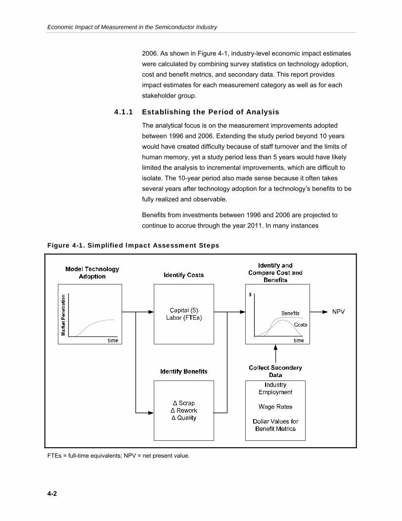
Economic Impact of Measurement in the Semiconductor Industry
2006. As shown in Figure 4-1, industry-level economic impact estimates were calculated by combining survey statistics on technology adoption, cost and benefit metrics, and secondary data. This report provides impact estimates for each measurement category as well as for each stakeholder group.
4.1.1 Establishing the Period of Analysis
The analytical focus is on the measurement improvements adopted between 1996 and 2006. Extending the study period beyond 10 years would have created difficulty because of staff turnover and the limits of human memory, yet a study period less than 5 years would have likely limited the analysis to incremental improvements, which are difficult to isolate. The 10-year period also made sense because it often takes several years after technology adoption for a technology’s benefits to be fully realized and observable.
Benefits from investments between 1996 and 2006 are projected to continue to accrue through the year 2011. In many instances
Figure 4-1. Simplified Impact Assessment Steps
FTEs = full-time equivalents; NPV = net present value.
4-2

Section 4 — Assessing the Impacts of Measurement Improvements
respondents indicated that the measurement investments made over the past 10 years would be relevant for many years into the future. However, because of the dynamic nature of the industry and in an effort to be conservative, the study used only a 5-year projection of benefits.
4.1.2 Estimating Benefits and Costs Relative to the Measurement Paradigm in Place in 1996
Measurement improvements were gradually adopted as new technologies and systems were developed and the data and practices central to their implementation were diffused. The beginning of the study period, therefore, represents a reference point. Benefits and costs were measured relative to the state-of-the-art measurement strategies in place at that time.
Measuring benefits and costs from the 1996 baseline required that interviewees provide operating parameters for that year and measure improvements relative to that baseline for each subsequent year. Conceptually this means that the analysis applied the 1996 measurement paradigm to each year in the study period and quantified benefits relative to that baseline. Experts assisted in charting the adoption of measurement improvements over time, which was necessary to ensure that benefit accruals were accurately timed.
The counterfactual scenario is that the measurement paradigm in place in 1995 would have persisted. The annual net change from the baseline represented the net benefit of the improvements for each year. For the purposes of this study, technology improvements cease in 2006, thus the technical impacts, and therefore economic benefits, are a fixed proportion of estimated unit sales from 2007 to 2011.
4.2 ESTIMATING MEASUREMENT EXPENDITURES, 1996 TO 2006 This study quantifies the expenditures stakeholders made between 1996 and 2006 on measurement equipment and process improvements13
within the following general categories:
• product design tools,
• software standards and interoperability,
• calibration and standard test methods,
• ex situ process control techniques,
13Of note, estimated expenditures include R&D and production expenditures.
4-3

Economic Impact of Measurement in the Semiconductor Industry
4.2.1
• in situ process control techniques, and
• quality assurance.14
The resulting time series of costs represents the investment cost of accruing economic benefits. This section details
• how the adoption of new technologies was estimated to have occurred over time,
• how survey responses were normalized to ensure an apples-to-apples comparison among responses,
• the development of technical and economic impact metrics that captured spending, and
• how captured spending was disaggregated into one-time costs and ongoing expenses.
The majority of the data employed in this analysis were collected through a series of in-depth interviews and an Internet survey. The data collection process is not discussed in detail until Section 4.5, but the preceding methodology discussion necessarily references that survey process to illuminate calculation steps. A copy of the survey instrument is included as Appendix B of this report.
Technology Adoption
Information on technology adoption was collected through an Internet survey to determine when firms began to incorporate technologies and how diffusion progressed over time.
Survey data were used primarily for estimating average adoption curves for each technology and process change. These adoption curves provided insight into the types of measurement technologies being implemented and the timing of measurement investments. Firm-level responses were weighted by their respective sales figures to assemble a stakeholder group’s adoption curve.
For example, an IC design firm was asked what percentage of its design activities took advantage of new EDA tool features in 1996, 2001, and 2006. Earlier in the survey, the firm provided sales and employment data that, when combined with other individual firm estimates in the same stakeholder group and industry-level data, permitted the construction of a generalized technology adoption curve for the entire stakeholder group.
14Ex situ process control, in situ process control, and QA technologies were organized into subcategories by grouping similar process and technology changes.
4-4
Section 4 — Assessing the Impacts of Measurement Improvements
4.2.2 Normalization and Extrapolation of Survey Responses
Survey respondents provided data on their measurement expenditures in 1996, 2001, and 2006 (as a percentage of sales), as well as the timing of the adoption of new measurement technologies. Other time-series data they provided were sales revenues for their business unit and information on how their organization’s expenditures on new measurement technologies changed. Respondents were expressly asked to consider only new, not replacement, measurement technologies and systems and report that data to the best of their ability.
It was assumed that the sum of costs reported by participating firms was representative of the stakeholder group’s costs. Thus, stakeholder-level costs were developed by extrapolating participants’ data using their combined sales as compared with the stakeholder group’s total sales. Total industry expenditures were the sum of all stakeholder group estimates. Ultimately, the firms that provided information represented 82% of the semiconductor industry, as measured by 2006 industry revenues.
Industry sales revenue was obtained from the U.S. Census Bureau. The U.S. Census Manufacturing Industry Series, published every 5 years, is a source of aggregated industry statistics, such as industry size (employment), revenues, capital expenditures, and cost of materials broken out by North American Industry Classification System (NAICS) code. RTI used the Semiconductor and Other Device Manufacturing category (NAICS 334413) statistics to discern total revenue for back-end, front-end, and IC design firms. The Manufacturing Industry Series also provides a detailed breakdown of materials consumed by the industry. This information was used to estimate the revenue of chemical and material suppliers. The Semiconductor Machinery Manufacturing category (NAICS 333295) statistics were used to estimate equipment manufacturers’ revenue. RTI used the Census information to determine estimated revenue in each semiconductor stakeholder group.
RTI combined data obtained from Gartner with that of the Census to define industry revenue totals appropriately and, subsequently, to calculate costs and benefits. Gartner is one of the leading providers of technology-related market research. For the semiconductor industry, Gartner researchers collect and provide analysis on industry sales, for firms around the world and U.S. firms.
4-5
Economic Impact of Measurement in the Semiconductor Industry
4.2.3
4.2.4
Expenditure Categories
Respondents provided data on their spending on relevant measurement technologies and process changes within each of the six measurement categories as a percentage of sales. Note that respondents in different stakeholder groups provided data for different sets of measurement categories. Thus, RTI then developed expenditure estimates normalized by sales for each stakeholder group–measurement category combination (see Figure 4-2).
To capture investment expenditures, respondents reported their total measurement expenditures and then experts helped partition these into measurement investments (one-time expenditures on equipment, software, and installation) and variable expenditures (ongoing expenditures such as calibration materials and associated labor costs) at the measurement category level. Investment expenditures included the following:
• Measurement equipment: In some instances, measurement activities are conducted by stand-alone pieces of equipment. However, increasingly measurement capabilities are integrated into larger automated production systems. In these instances, respondents were asked to estimate the share of new equipment expenditures related to only the measurement technology.
• Software: EDA tools and associated new software packages represent a large investment expense, and all new equipment requires the integration of software systems to capture, analyze, and output measurement data.
• Installation, integration, and testing: Each piece of new equipment and software requires training, testing, physical and/or software installation, and integration with other equipment or software. The transition to a new tool or standard often occurs over several years, and it is not uncommon for installation and ramp-up costs to exceed the initial capital outlay.
Fixed versus Variable Expenditures
It was important to distinguish between one-time, fixed investment costs and recurring variable costs so that only relevant expenditures (i.e., those related to improved measurement technologies and standards) would be included in our analysis. However, none of the companies surveyed were able to partition measurement expenditures into one-time investment expenditures versus variable costs.
4-6
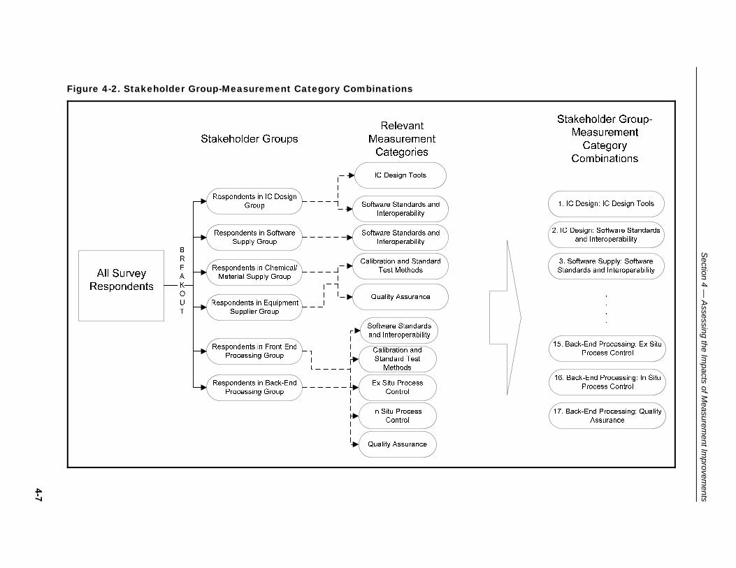
Section 4 —
Assessing the Im
pacts of Measurem
ent Improvem
ents
Figure 4-2. Stakeholder Group-Measurement Category Combinations
4-7

Economic Impact of Measurement in the Semiconductor Industry
As a result, industry experts were consulted to develop estimates of the relative share of variable to total expenditures. Industry experts unanimously agreed that investments in automation led to decreasing variable costs during our period of analysis (see Figure 4-3). Chapter 5 provides estimates of how the ratio of fixed to variable costs for each measurement category within expenditures on new measurement technologies and standards changed between 1996 and 2006. These estimates, based on expert interviews, provide support for breaking out annual variable and fixed costs between 1996 and 2006. And assuming, for simplicity, that the estimated ratio of variable to fixed costs in 2006 will remain static into the future, such estimates allow the calculation of variable costs between 2007 and 2011, when we stop calculating benefits.
Figure 4-3. General Measurement Expenditure Trends over Time, Variable versus Fixed
Expenditures $
Variable Costs Associated with New and Old Measurement
1996 2006 Time
Fixed Investment in Measurement
4-8
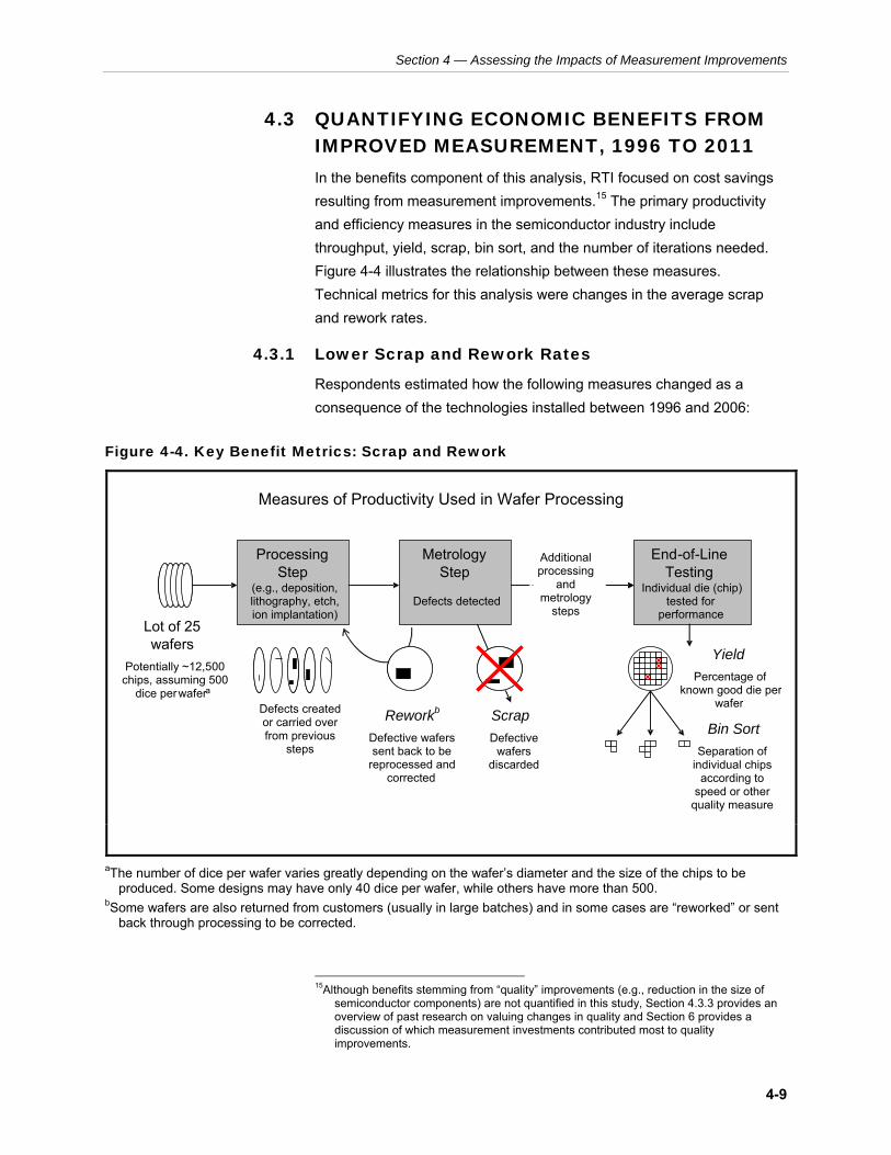
Section 4 — Assessing the Impacts of Measurement Improvements
4.3 QUANTIFYING ECONOMIC BENEFITS FROM IMPROVED MEASUREMENT, 1996 TO 2011 In the benefits component of this analysis, RTI focused on cost savings resulting from measurement improvements.15 The primary productivity and efficiency measures in the semiconductor industry include throughput, yield, scrap, bin sort, and the number of iterations needed. Figure 4-4 illustrates the relationship between these measures. Technical metrics for this analysis were changes in the average scrap and rework rates.
4.3.1 Lower Scrap and Rework Rates
Respondents estimated how the following measures changed as a consequence of the technologies installed between 1996 and 2006:
Figure 4-4. Key Benefit Metrics: Scrap and Rework
aThe number of dice per wafer varies greatly depending on the wafer’s diameter and the size of the chips to be produced. Some designs may have only 40 dice per wafer, while others have more than 500.
bSome wafers are also returned from customers (usually in large batches) and in some cases are “reworked” or sent back through processing to be corrected.
Processing Step
(e.g., deposition, lithography, etch, ion implantation)
Defects created or carried over from previous
steps
Reworkb
Defective wafers sent back to be
reprocessed and corrected
Scrap Defective
wafers discarded
Lot of 25 wafers
Potentially ~12,500 chips, assuming 500
dice per wafera
Yield Percentage of
known good die per wafer
Metrology Step
Defects detected
End - of- Line Testing
Individual die (chip) tested for
performance
Bin Sort Separation of
individual chips according to
speed or other quality measure
Additional processing
and metrology
steps
Measures of Productivity Used in Wafer Processing
15Although benefits stemming from “quality” improvements (e.g., reduction in the size of semiconductor components) are not quantified in this study, Section 4.3.3 provides an overview of past research on valuing changes in quality and Section 6 provides a discussion of which measurement investments contributed most to quality improvements.
4-9
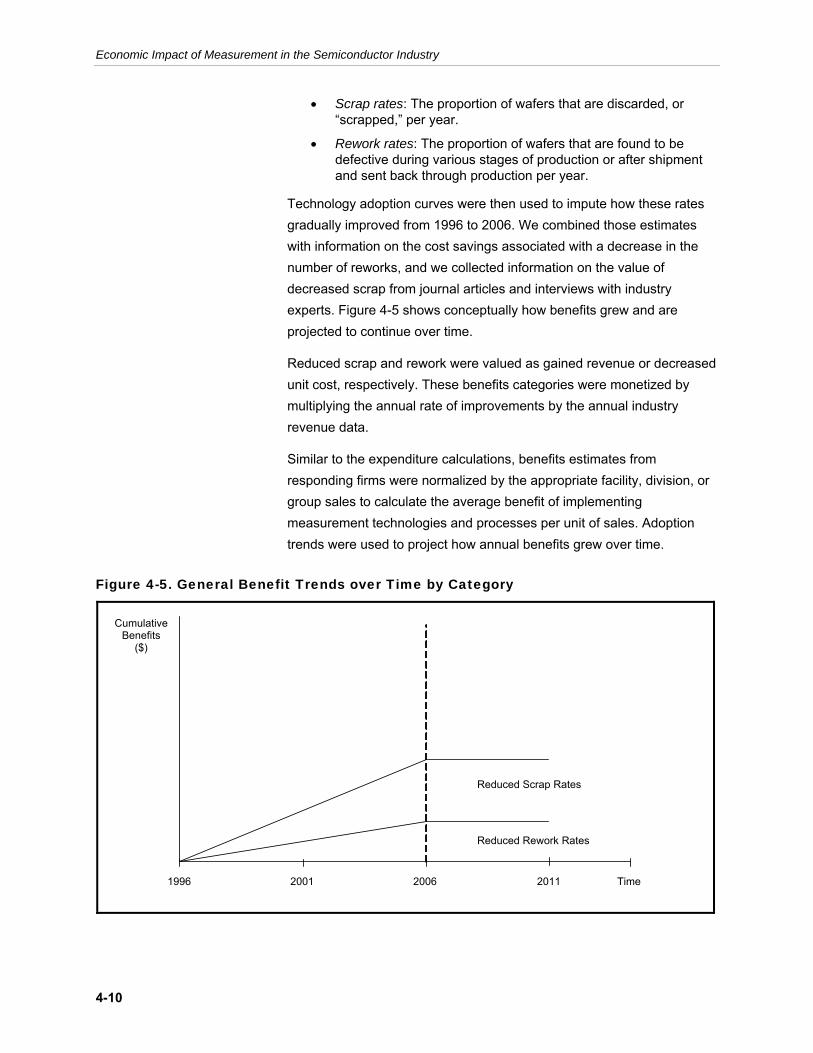
Economic Impact of Measurement in the Semiconductor Industry
• Scrap rates: The proportion of wafers that are discarded, or “scrapped,” per year.
• Rework rates: The proportion of wafers that are found to be defective during various stages of production or after shipment and sent back through production per year.
Technology adoption curves were then used to impute how these rates gradually improved from 1996 to 2006. We combined those estimates with information on the cost savings associated with a decrease in the number of reworks, and we collected information on the value of decreased scrap from journal articles and interviews with industry experts. Figure 4-5 shows conceptually how benefits grew and are projected to continue over time.
Reduced scrap and rework were valued as gained revenue or decreased unit cost, respectively. These benefits categories were monetized by multiplying the annual rate of improvements by the annual industry revenue data.
Similar to the expenditure calculations, benefits estimates from responding firms were normalized by the appropriate facility, division, or group sales to calculate the average benefit of implementing measurement technologies and processes per unit of sales. Adoption trends were used to project how annual benefits grew over time.
Figure 4-5. General Benefit Trends over Time by Category
Cumulative Benefits
($)
1996 2001 2011 Time 2006
Reduced Scrap Rates
Reduced Rework Rates
4-10
Section 4 — Assessing the Impacts of Measurement Improvements
Reduced scrap and rework are benefits that relate most directly to front-end and back-end manufacturing activities. While these measures do not capture all productivity benefits related to measurement improvements, experts indicated that these two rates account for the largest proportion of easily quantifiable benefits.
4.3.2 Quality Improvements
Given the rapid rate of innovation in the industry, this study did not seek to quantify the improvement in product quality from improved measurement. Apportioning advances in product quality between measurement improvements and product innovation was not possible. Although this may result in an underestimation of the value of improvements, it is likely that the majority of product quality improvements are rooted in innovation.
Enhanced measurement has played an important role in the dramatic improvements in the quality and performance of semiconductors between 1996 and 2006. However, monetizing these benefits is difficult because changes in the value-added over time are attributable to both generic technology and infratechnology advances, with the two technology elements acting in a complementary manner (Tassey, 2005).
In this regard, the science and engineering literatures suggest that the semiconductor devices of today could not have been produced using the measurement capabilities available in 1996. Developments between 1996 and 2006 include a reduction in features sizes, an increase in wafer size, and an improvement in materials used for production. Based on these changes, the number of bits of data that may be stored on a chip (density) has increased, internal clock speed (in MHz) has increased, computing power (in millions of instructions per second) has increased, and the number of transistors on a chip for microprocessors has increased (Grimm, 1998). Each of these characteristics is affected by measurement to a different degree.16 The decrease in the space between semiconductor components, which enables more bits to be stored on a chip, seems to have the most direct link to improvements in measurement because it depends on very precise physical measurements.
16Precision measurement cannot claim to be the only enabler of such improvements; proprietary lithography techniques, design software, front-end processes, interconnect technologies, and even advancements in IT computing power and data storage capacities have all played a role.
4-11
Economic Impact of Measurement in the Semiconductor Industry
Although it is impossible to pinpoint any one measurement innovation as the key factor in quality improvement, stakeholders and experts estimated the percentage of quality improvement attributable to each measurement category to provide a relative benefit metric. If a total benefit figure were available, it could be used to calculate explicit benefits by measurement category. However, only one study provides a hard monetary value for quality improvements. In this study, published by Motorola, the authors assigned a monetary value to a specific quality improvement and estimated an average revenue gain of more than $7 per chip for each nanometer reduction of CDs (Gerold et al., 1997).
Price measures, often estimated by hedonic functions, are one common way to measure quality improvement. One study by Grimm (1998) used a hedonic approach to construct quality-adjusted price indexes for several types of semiconductors, and his results may be useful for our analysis. In this study, unit prices were regressed against various quality characteristics. The most statistically significant variables for microprocessors included the ability to perform multitasking operations, PC support/control capabilities, the existence of external memory-management circuit and internal memory-management unit, and year of the observation. In a hedonic regression for DRAM (memory), the most statistically significant variables included density, a dummy variable indicating the use of DRAM technology, and a nonlinear variable representing the age of the chip’s density class. It may be possible to use coefficients from the hedonic regressions to infer the marginal value of these specific characteristics, which have changed over our period of analysis. However, the hedonic approach can be difficult and the results easily misconstrued. The fact that technical change permits the buyer to perform tasks that were not technologically possible at any price in the earlier period suggests that this gain cannot be effectively measured with hedonic functions alone (Triplett, 2000).17
A study by Jula (2001) looks at two different metrics to measure the performance of metrology methods: revenue per wafer and revenue per day. By measuring revenue generated per wafer, one can capture the quality of the products produced from that wafer. Thus, the long-run average would allow measurement of the quality of the product and the service. Alternatively, revenue per day measures the combined effect of yield, throughput, and product quality.
17Hedonic function would not capture the improvement at the upper end of the product space, where the earlier period cost was infinity.
4-12

Section 4 — Assessing the Impacts of Measurement Improvements
Additional research discusses the common practice by industry members and researchers of looking at the difference between a constant-quality index and an average price series to determine an informal measure of quality.18 Aizcorbe (2002) suggests a superlative index, the Tornquist, that captures quality changes that result from both turnover (difference in means with and without the new good19) and from mix-shift (changes in relative importance of existing goods) among existing goods.
Improvements in semiconductors also have had a significant impact in many areas. For example, semiconductors play a very important role in supporting high data rate networks, high-end computing, and validated software that can mine and extract useful information from massive data sets and from many measurement technologies, particularly those for nanoscale structures and manufacturing processes. Quantification of such benefits would be speculative.
4.3.3 Benefits Estimation Calculation
Benefits from reduced scrap and rework rates were based on company estimates provided during interviews and the Internet survey. These benefits were found only to accrue to front-end and back-end firms.
In the case of scrap, respondents provided detailed data on their annual scrap rates, as a percentage of sales, in 2006 and 1996. Different respondents’ estimates were weighted by their sales and then averaged to derive an industry scrap rate estimate for those 2 years. Annual scrap rates were estimated to have changed in a linear fashion between 1996 and 2006. Actual scrap costs were calculated in each year using actual estimated scrap rates and overall sales for front-end and back-end firms. Counterfactual scrap costs were calculated using the average estimated 1996 scrap rate multiplied by the same annual sales figures. Reduced scrap benefits were calculated as the difference between the counterfactual scrap costs and the actual scrap costs.
Reduced rework benefits were calculated by estimating both the average cost of reworking of a unit and how often rework occurred in 1996 and 2006. First, firms provided estimates of the average cost of reworking a unit (i.e., a wafer) as a percentage of the sales of that unit. Estimates for 1996 and 2006 were weighted and averaged as in the case of rework. If these percentages were multiplied by relevant industry sales, the
18The idea is that a price index holds quality constant and average price series does not. The difference between the two would provide a measure of quality change.
19A new good in the context of the article means a new generation of the chip. For instance, an 80386 processor would be considered a new good for the 80286 processor market.
4-13
Economic Impact of Measurement in the Semiconductor Industry
resulting dollar figure would be the cost if all units were reworked. Second, interviews were used to capture information on how often rework occurs. Estimates from 1996 and 2006 were given as percentage of output. Annual estimates of average cost and rate of occurrence were calculated by assuming a linear change trend.
Actual rework costs were calculated by multiplying industry sales by the average cost as a percentage of sales and by the average rate of rework. Counterfactual rework costs were calculated in the same way using 1996 cost and rework rate figures. Reduced rework benefits were calculated as the difference between counterfactual rework costs and the actual rework costs.
4.3.4 Benefits Accrual by Stakeholder Group
Productivity benefits were investigated for stakeholder groups beyond front-end and back-end processing firms. However, IC designers, chemical and material suppliers, and equipment suppliers all indicated that the benefits of their measurement investments were realized by the front-end and back-end processing firms.
These stakeholders viewed their advances in measurement as features embedded in their products and not as technologies that enhanced design or production efficiency. These stakeholder groups said that implementation of measurement advances into their products and services was necessary for them to maintain their market share.
Any benefits were offset by cost increases. In many instances, they increased the cost of producing or developing their products and services as a result of increased complexity, and the benefits of the improved products and services they supplied simply flowed to their customers.
4.4 CALCULATING MEASURES OF ECONOMIC RETURN Three benchmark measures—benefit-to-cost ratio (BCR), net present value (NPV), and internal rate of return (IRR)—provide estimates of the net economic benefits generated by improved measurement technologies.
4-14
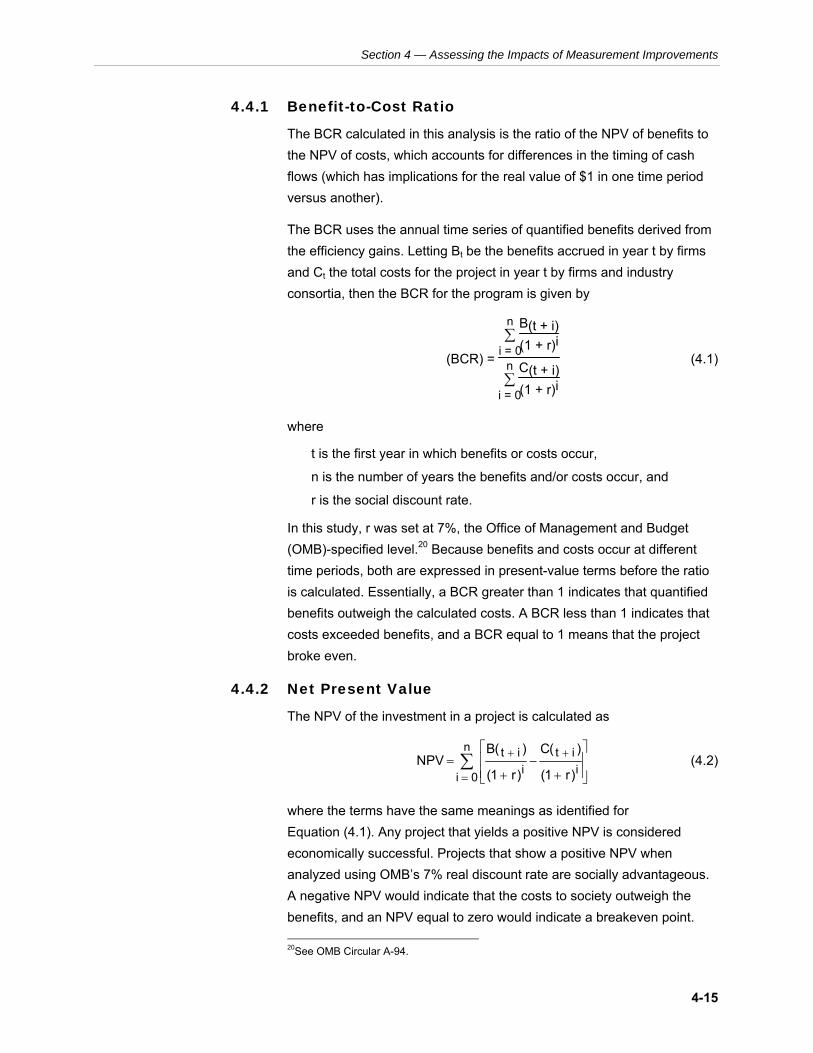
Section 4 — Assessing the Impacts of Measurement Improvements
4.4.1 Benefit-to-Cost Ratio
The BCR calculated in this analysis is the ratio of the NPV of benefits to the NPV of costs, which accounts for differences in the timing of cash flows (which has implications for the real value of $1 in one time period versus another).
The BCR uses the annual time series of quantified benefits derived from the efficiency gains. Letting Bt be the benefits accrued in year t by firms and Ct the total costs for the project in year t by firms and industry consortia, then the BCR for the program is given by
n B(t + i)∑
(1 + r)ii = 0 (BCR) = (4.1)n C(t + i)∑
(1 + r)ii = 0
where
t is the first year in which benefits or costs occur,
n is the number of years the benefits and/or costs occur, and
r is the social discount rate.
In this study, r was set at 7%, the Office of Management and Budget (OMB)-specified level.20 Because benefits and costs occur at different time periods, both are expressed in present-value terms before the ratio is calculated. Essentially, a BCR greater than 1 indicates that quantified benefits outweigh the calculated costs. A BCR less than 1 indicates that costs exceeded benefits, and a BCR equal to 1 means that the project broke even.
4.4.2 Net Present Value
The NPV of the investment in a project is calculated as
n ⎡B( t + i ) C( t + i )⎤ NPV = ∑ ⎢ − ⎥ (4.2) i = 0 ⎢⎣(1 + r)i (1 + r)i ⎥⎦
where the terms have the same meanings as identified for Equation (4.1). Any project that yields a positive NPV is considered economically successful. Projects that show a positive NPV when analyzed using OMB’s 7% real discount rate are socially advantageous. A negative NPV would indicate that the costs to society outweigh the benefits, and an NPV equal to zero would indicate a breakeven point.
20See OMB Circular A-94.
4-15
Economic Impact of Measurement in the Semiconductor Industry
4.4.3 Internal Rate of Return
The IRR on an investment should be interpreted as the percentage yield on an R&D project over the life of the project, often multiple years (Tassey, 2003). In mathematical terms, the IRR is the value of r that sets the NPV equal to zero in Equation (4.2) or results in a benefit-cost ratio of 1 in Equation (4.1).
The IRR’s value can be compared with conventional rates of return for comparable or alternative investments. Risk-free capital investments such as government bonds can be expected to yield rates of return under 5% in real terms, while equities seldom return more than 10% over an extended period of time. In academic studies of the diffusion of new technologies, however, real rates of return of 100% or more have been found for significant advances with broad social benefits. It should be noted that, in cases for which costs exceed benefits, an IRR cannot be calculated.
4.5 DATA COLLECTION ACTIVITIES Information was collected using three modes: in-person and telephone interviews, Internet-based surveys, and a review of secondary data sources. Data were collected from companies that represent 82% of the semiconductor industry, as measured by 2006 industry revenues. Disaggregated information on participation at the stakeholder group level, including the number of responding firms, was withheld to prevent inadvertent disclosure of identifiable firms’ participation.
4.5.1 Telephone and On-Site Interviews
Approximately 34 on-site and telephone interviews were conducted. These interviews included detailed questions related to the costs and benefits of measurement improvements. Interview participants were also asked to complete the online survey instrument. The key information collected during this process included
• costs (measurement improvement expenditures),
• benefits (productivity savings and quality improvements) associated with each measurement category,
• timing of these expenditures and benefits, and
• employment and sales.
In addition to these interviews, we held multiple rounds of discussions with experts at industry associations and consortia such as SEMI,
4-16
Section 4 — Assessing the Impacts of Measurement Improvements
SEMATECH, SRC, and NIST to estimate the monetary gains resulting from increases in throughput and yield, decreases in scrap, and decreases in the number of iterations needed to build a semiconductor.
Industry experts and stakeholders also helped develop a measurement improvement classification system that resonated with stakeholders who participated in the data collection exercises. These experts included Dr. Randy Goodall, Associate Director of Manufacturing Methods and Productivity at SEMATECH; Dr. Alain Diebold, Senior Fellow at SEMATECH; Bob Johnson, Research Vice President at Gartner; Dr. James Hutchby, Director of Device Sciences at SRC; and Dr. Steve Knight, Dr. Herb Bennett, and Dr. Jack Martinez at NIST.
4.5.2 Internet-Based Survey Data Collection
An Internet survey instrument accessed by more than 140 individuals was constructed to collect information on adoption trends. Respondents were prompted to provide general information about their firm such as employment, revenue, position in the supply chain, type of device produced/supplied, and level of international operations. Respondents were then asked to approximate the percentage (i.e., level of adoption) of their activities or processes that incorporated the technologies that were selected in each of the six measurement categories for 1996, 2001, 2006, and 2011. This information was used to construct annual spending and annual benefits observation estimates for each stakeholder group– measurement category combination, which is based on the timing and market penetration of all measurement technology and process improvements in the industry.
4.5.3 Secondary Data Collection
Information was collected from secondary data sources to help monetize technical impact metrics obtained during the interviews and develop industry-level impact estimates from company-level survey and interview data. Data sources included the U.S. Bureau of Labor Statistics and Census, private technology research institutions such as Gartner, industry consortia and trade groups, and academic literature.
4.5.4 Data Collection Challenges
Data collection for this study was particularly difficult for two reasons. First, the industry has spent significant time and effort developing measurement technologies and coordinating investments to reduce feature sizes and increase wafer sizes. As such, many stakeholders
4-17
Economic Impact of Measurement in the Semiconductor Industry
were not immediately concerned with soliciting government support for standardization and technology development efforts, unlike other industries in which adequate investment in standards and industry coordination remain major impediments.
Second, the international nature of the industry created problems in data collection because multinational companies had trouble providing information for only their U.S. operations. In general, the semiconductor industry operates without consideration of national or geographic borders when making investment and production decisions, except for logistics of shipments and any country-specific regulations. However, this study focused on the costs and benefits of measurement improvements specifically borne by and appropriated by U.S.-based companies within the semiconductor industry.
4-18
Measurement Technology Adoption 5 and Expenditures
This chapter presents analysis results for estimating industry and consortia expenditures on measurement improvements between 1996 and 2006. Included are survey results on historical technology adoption trends and expenditures for new standards, technologies, and processes by measurement category and by stakeholder group. Note that all references to measurement expenditures refer to expenditures on new technologies and standards implemented between 1996 and 2006, as opposed to fixed and variable costs on older generation technology and standards.
Section 5.1 presents results at a summary level discussing broad trends across all stakeholders and measurement categories. Section 5.2 provides an in-depth discussion of technology expenditures and trends within each measurement category.
5.1 SUMMARY EXPENDITURE AND ADOPTION DATA, 1996 TO 2006 Between 1996 and 2006, expenditures on improved measurement technologies, systems, and processes increased relatively linearly. Although the industry slowed between 2000 and 2002 and there was a shift in semiconductor design and production to outside the United States, firms continued their spending on new measurement technologies. All tables and figures in this section are denominated in real 2006 dollars.
5.1.1 Inflation-Adjusted Industry Sales Revenues
Table 5-1 shows the approximate revenues of the main stakeholder groups in the semiconductor industry in 1996 and 2006, as well as the percentage change between the two values. Recall that many
5-1
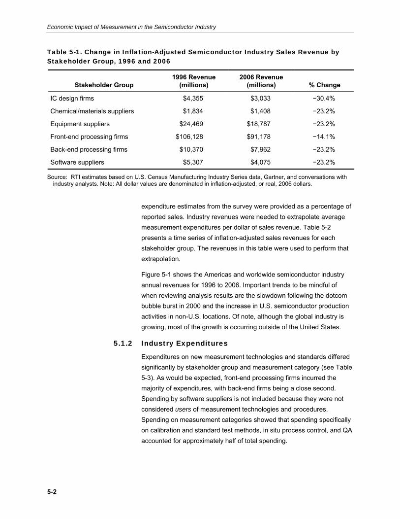
Economic Impact of Measurement in the Semiconductor Industry
Table 5-1. Change in Inflation-Adjusted Semiconductor Industry Sales Revenue by Stakeholder Group, 1996 and 2006
1996 Revenue 2006 Revenue Stakeholder Group (millions) (millions) % Change
IC design firms $4,355 $3,033 −30.4%
Chemical/materials suppliers $1,834 $1,408 −23.2%
Equipment suppliers $24,469 $18,787 −23.2%
Front-end processing firms $106,128 $91,178 −14.1%
Back-end processing firms $10,370 $7,962 −23.2%
Software suppliers $5,307 $4,075 −23.2%
Source: RTI estimates based on U.S. Census Manufacturing Industry Series data, Gartner, and conversations with industry analysts. Note: All dollar values are denominated in inflation-adjusted, or real, 2006 dollars.
expenditure estimates from the survey were provided as a percentage of reported sales. Industry revenues were needed to extrapolate average measurement expenditures per dollar of sales revenue. Table 5-2 presents a time series of inflation-adjusted sales revenues for each stakeholder group. The revenues in this table were used to perform that extrapolation.
Figure 5-1 shows the Americas and worldwide semiconductor industry annual revenues for 1996 to 2006. Important trends to be mindful of when reviewing analysis results are the slowdown following the dotcom bubble burst in 2000 and the increase in U.S. semiconductor production activities in non-U.S. locations. Of note, although the global industry is growing, most of the growth is occurring outside of the United States.
5.1.2 Industry Expenditures
Expenditures on new measurement technologies and standards differed significantly by stakeholder group and measurement category (see Table 5-3). As would be expected, front-end processing firms incurred the majority of expenditures, with back-end firms being a close second. Spending by software suppliers is not included because they were not considered users of measurement technologies and procedures. Spending on measurement categories showed that spending specifically on calibration and standard test methods, in situ process control, and QA accounted for approximately half of total spending.
5-2
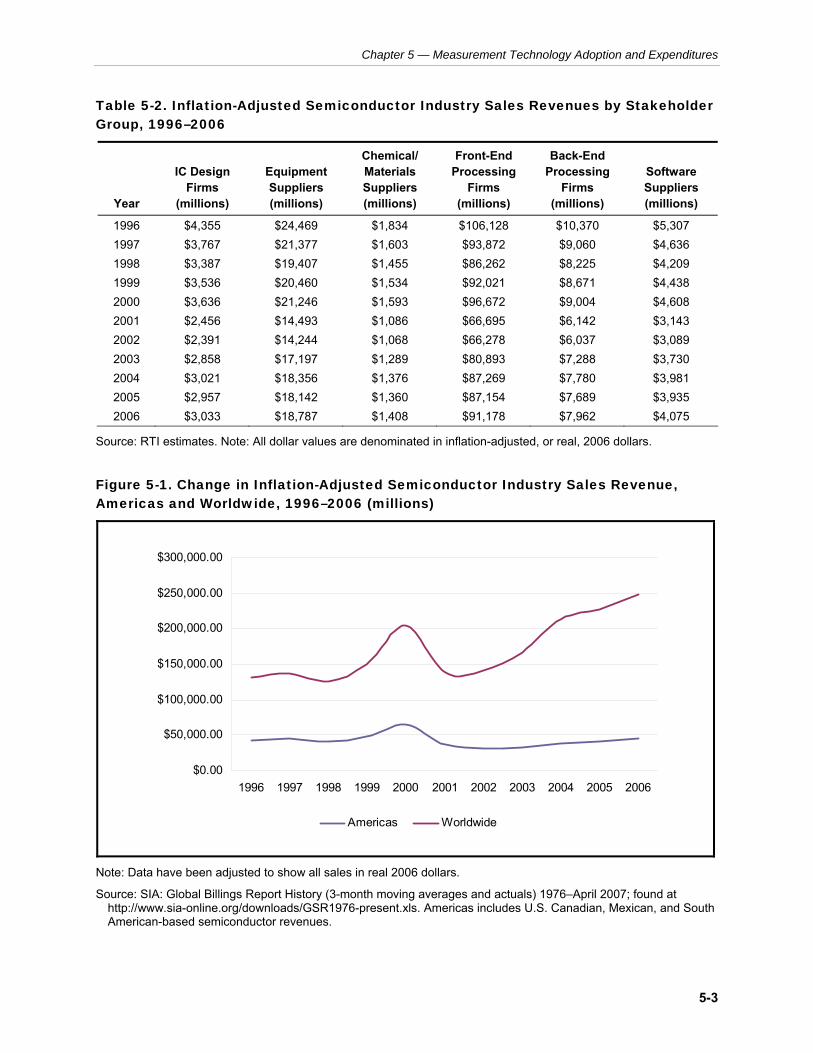
Chapter 5 — Measurement Technology Adoption and Expenditures
Table 5-2. Inflation-Adjusted Semiconductor Industry Sales Revenues by Stakeholder Group, 1996–2006
Chemical/ Front-End Back-End IC Design Equipment Materials Processing Processing Software
Firms Suppliers Suppliers Firms Firms Suppliers Year (millions) (millions) (millions) (millions) (millions) (millions)
1996 $4,355 $24,469 $1,834 $106,128 $10,370 $5,307 1997 $3,767 $21,377 $1,603 $93,872 $9,060 $4,636 1998 $3,387 $19,407 $1,455 $86,262 $8,225 $4,209 1999 $3,536 $20,460 $1,534 $92,021 $8,671 $4,438 2000 $3,636 $21,246 $1,593 $96,672 $9,004 $4,608 2001 $2,456 $14,493 $1,086 $66,695 $6,142 $3,143 2002 $2,391 $14,244 $1,068 $66,278 $6,037 $3,089 2003 $2,858 $17,197 $1,289 $80,893 $7,288 $3,730 2004 $3,021 $18,356 $1,376 $87,269 $7,780 $3,981 2005 $2,957 $18,142 $1,360 $87,154 $7,689 $3,935 2006 $3,033 $18,787 $1,408 $91,178 $7,962 $4,075
Source: RTI estimates. Note: All dollar values are denominated in inflation-adjusted, or real, 2006 dollars.
Figure 5-1. Change in Inflation-Adjusted Semiconductor Industry Sales Revenue, Americas and Worldwide, 1996–2006 (millions)
$0.00
$50,000.00
$100,000.00
$150,000.00
$200,000.00
$250,000.00
$300,000.00
1996 1997 1998 1999 2000 2001 2002 2003 2004 2005 2006
Americas Worldwide
Note: Data have been adjusted to show all sales in real 2006 dollars.
Source: SIA: Global Billings Report History (3-month moving averages and actuals) 1976–April 2007; found at http://www.sia-online.org/downloads/GSR1976-present.xls. Americas includes U.S. Canadian, Mexican, and South American-based semiconductor revenues.
5-3
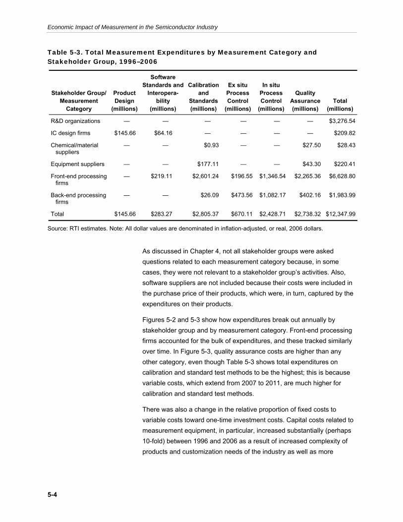
Economic Impact of Measurement in the Semiconductor Industry
Table 5-3. Total Measurement Expenditures by Measurement Category and Stakeholder Group, 1996–2006
Software Standards and Calibration Ex situ In situ
Stakeholder Group/ Product Interopera- and Process Process Quality Measurement Design bility Standards Control Control Assurance Total
Category (millions) (millions) (millions) (millions) (millions) (millions) (millions)
R&D organizations — — — — — — $3,276.54
IC design firms $145.66 $64.16 — — — — $209.82
Chemical/material — — $0.93 — — $27.50 $28.43 suppliers
Equipment suppliers — — $177.11 — — $43.30 $220.41
Front-end processing — $219.11 $2,601.24 $196.55 $1,346.54 $2,265.36 $6,628.80 firms
Back-end processing — — $26.09 $473.56 $1,082.17 $402.16 $1,983.99 firms
Total $145.66 $283.27 $2,805.37 $670.11 $2,428.71 $2,738.32 $12,347.99
Source: RTI estimates. Note: All dollar values are denominated in inflation-adjusted, or real, 2006 dollars.
As discussed in Chapter 4, not all stakeholder groups were asked questions related to each measurement category because, in some cases, they were not relevant to a stakeholder group’s activities. Also, software suppliers are not included because their costs were included in the purchase price of their products, which were, in turn, captured by the expenditures on their products.
Figures 5-2 and 5-3 show how expenditures break out annually by stakeholder group and by measurement category. Front-end processing firms accounted for the bulk of expenditures, and these tracked similarly over time. In Figure 5-3, quality assurance costs are higher than any other category, even though Table 5-3 shows total expenditures on calibration and standard test methods to be the highest; this is because variable costs, which extend from 2007 to 2011, are much higher for calibration and standard test methods.
There was also a change in the relative proportion of fixed costs to variable costs toward one-time investment costs. Capital costs related to measurement equipment, in particular, increased substantially (perhaps 10-fold) between 1996 and 2006 as a result of increased complexity of products and customization needs of the industry as well as more
5-4
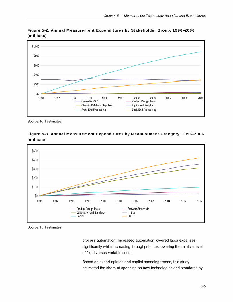
Chapter 5 — Measurement Technology Adoption and Expenditures
Figure 5-2. Annual Measurement Expenditures by Stakeholder Group, 1996–2006 (millions)
$1,000
$800
$600
$400
$200
$0 1996 1997 1998 1999 2000 2001 2002 2003 2004 2005 2006
Consortia R&D Product Design Tools Chemical/Material Suppliers Equipment Suppliers Front-End Processing Back-End Processing
Source: RTI estimates.
Figure 5-3. Annual Measurement Expenditures by Measurement Category, 1996–2006 (millions)
$500
$400
$300
$200
$100
$0 1996 1997 1998 1999 2000 2001 2002 2003 2004 2005 2006
Product Design Tools Software Standards Calibration and Standards In-Situ Ex-Situ QA
Source: RTI estimates.
process automation. Increased automation lowered labor expenses significantly while increasing throughput, thus lowering the relative level of fixed versus variable costs.
Based on expert opinion and capital spending trends, this study estimated the share of spending on new technologies and standards by
5-5
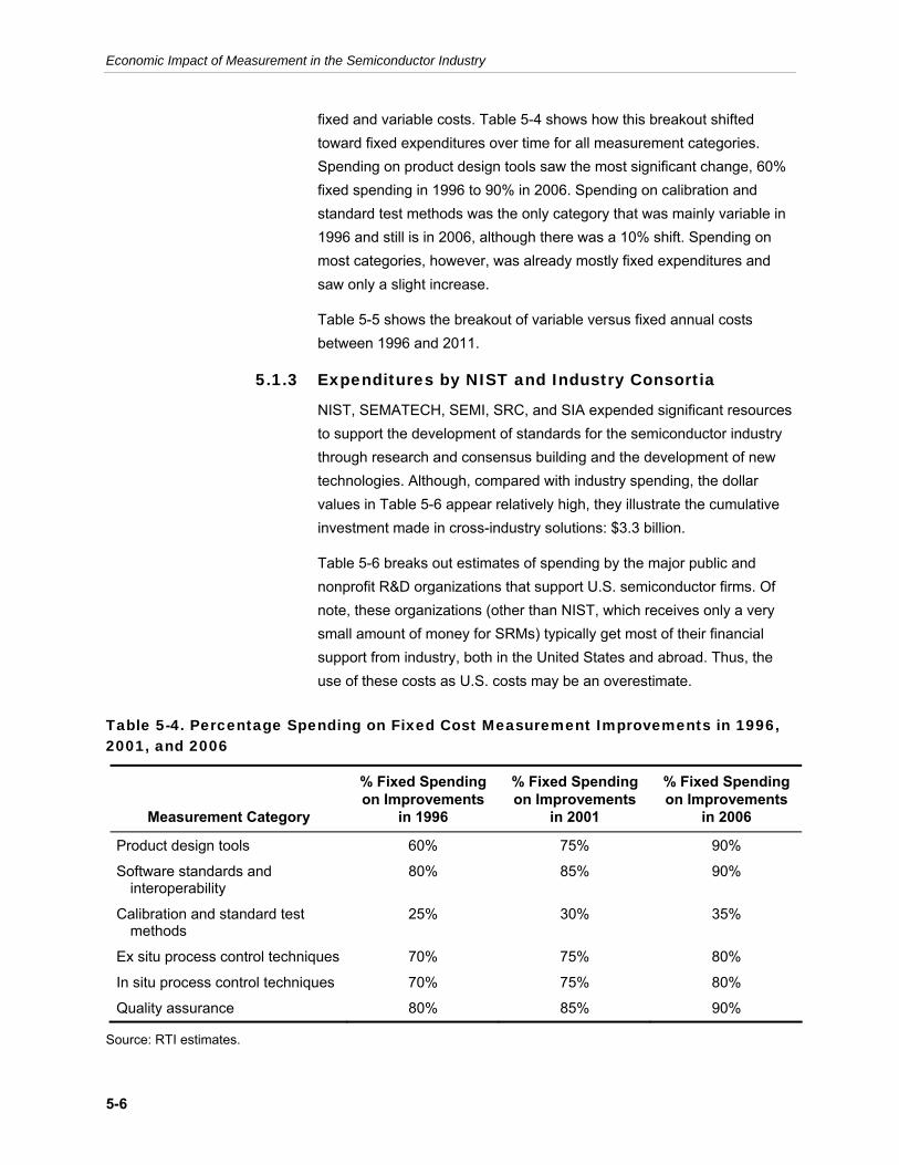
Economic Impact of Measurement in the Semiconductor Industry
fixed and variable costs. Table 5-4 shows how this breakout shifted toward fixed expenditures over time for all measurement categories. Spending on product design tools saw the most significant change, 60% fixed spending in 1996 to 90% in 2006. Spending on calibration and standard test methods was the only category that was mainly variable in 1996 and still is in 2006, although there was a 10% shift. Spending on most categories, however, was already mostly fixed expenditures and saw only a slight increase.
Table 5-5 shows the breakout of variable versus fixed annual costs between 1996 and 2011.
5.1.3 Expenditures by NIST and Industry Consortia
NIST, SEMATECH, SEMI, SRC, and SIA expended significant resources to support the development of standards for the semiconductor industry through research and consensus building and the development of new technologies. Although, compared with industry spending, the dollar values in Table 5-6 appear relatively high, they illustrate the cumulative investment made in cross-industry solutions: $3.3 billion.
Table 5-6 breaks out estimates of spending by the major public and nonprofit R&D organizations that support U.S. semiconductor firms. Of note, these organizations (other than NIST, which receives only a very small amount of money for SRMs) typically get most of their financial support from industry, both in the United States and abroad. Thus, the use of these costs as U.S. costs may be an overestimate.
Table 5-4. Percentage Spending on Fixed Cost Measurement Improvements in 1996, 2001, and 2006
% Fixed Spending % Fixed Spending % Fixed Spending on Improvements on Improvements on Improvements
Measurement Category in 1996 in 2001 in 2006
Product design tools 60% 75% 90%
Software standards and 80% 85% 90% interoperability
Calibration and standard test 25% 30% 35% methods
Ex situ process control techniques 70% 75% 80%
In situ process control techniques 70% 75% 80%
Quality assurance 80% 85% 90%
Source: RTI estimates.
5-6
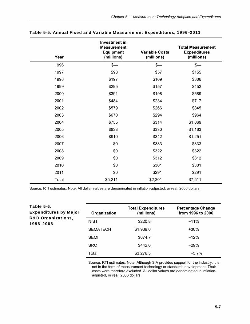
Chapter 5 — Measurement Technology Adoption and Expenditures
Table 5-5. Annual Fixed and Variable Measurement Expenditures, 1996–2011
Investment in Measurement Total Measurement
Equipment Variable Costs Expenditures Year (millions) (millions) (millions)
1996 $— $— $—
1997 $98 $57 $155
1998 $197 $109 $306
1999 $295 $157 $452
2000 $391 $198 $589
2001 $484 $234 $717
2002 $579 $266 $845
2003 $670 $294 $964
2004 $755 $314 $1,069
2005 $833 $330 $1,163
2006 $910 $342 $1,251
2007 $0 $333 $333
2008 $0 $322 $322
2009 $0 $312 $312
2010 $0 $301 $301
2011 $0 $291 $291
Total $5,211 $2,301 $7,511
Source: RTI estimates. Note: All dollar values are denominated in inflation-adjusted, or real, 2006 dollars.
Table 5-6. Expenditures by Major R&D Organizations, 1996–2006
Organization
NIST
Total Expenditures (millions)
$220.8
Percentage Change from 1996 to 2006
−11%
SEMATECH $1,939.0 +30%
SEMI $674.7 −12%
SRC $442.0 −29%
Total $3,276.5 −5.7%
Source: RTI estimates. Note: Although SIA provides support for the industry, it is not in the form of measurement technology or standards development. Their costs were therefore excluded. All dollar values are denominated in inflation-adjusted, or real, 2006 dollars.
5-7
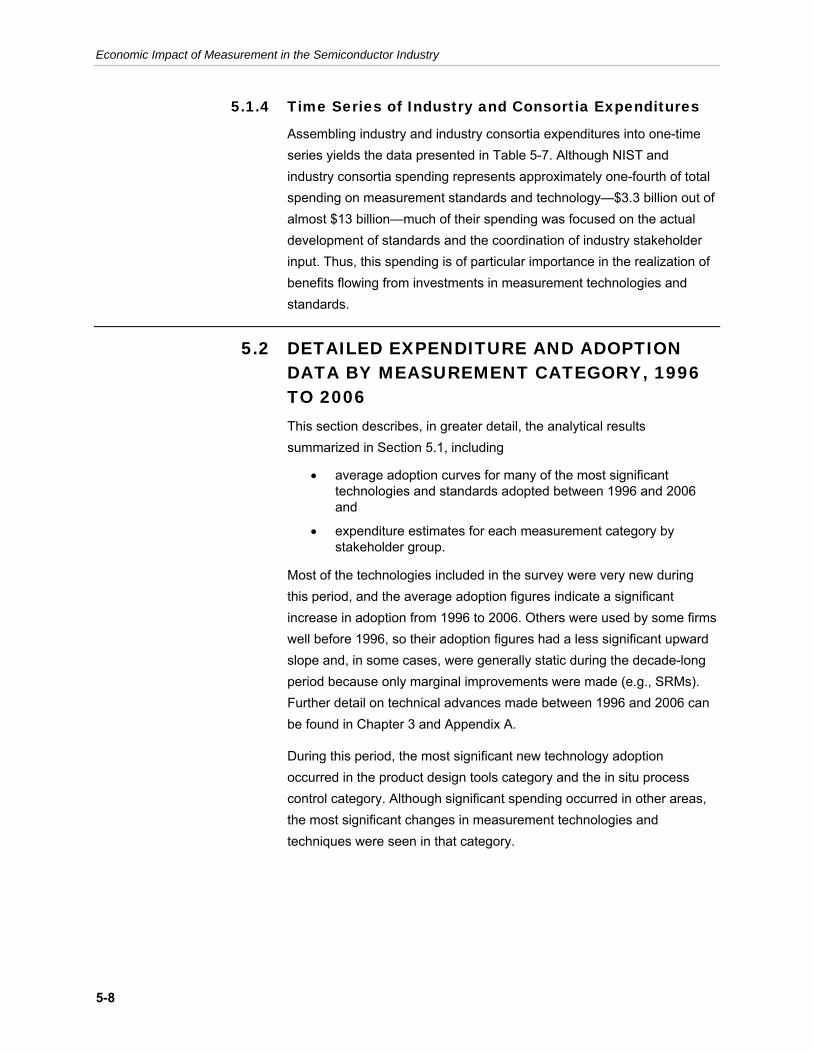
Economic Impact of Measurement in the Semiconductor Industry
5.1.4 Time Series of Industry and Consortia Expenditures
Assembling industry and industry consortia expenditures into one-time series yields the data presented in Table 5-7. Although NIST and industry consortia spending represents approximately one-fourth of total spending on measurement standards and technology—$3.3 billion out of almost $13 billion—much of their spending was focused on the actual development of standards and the coordination of industry stakeholder input. Thus, this spending is of particular importance in the realization of benefits flowing from investments in measurement technologies and standards.
5.2 DETAILED EXPENDITURE AND ADOPTION DATA BY MEASUREMENT CATEGORY, 1996 TO 2006 This section describes, in greater detail, the analytical results summarized in Section 5.1, including
• average adoption curves for many of the most significant technologies and standards adopted between 1996 and 2006 and
• expenditure estimates for each measurement category by stakeholder group.
Most of the technologies included in the survey were very new during this period, and the average adoption figures indicate a significant increase in adoption from 1996 to 2006. Others were used by some firms well before 1996, so their adoption figures had a less significant upward slope and, in some cases, were generally static during the decade-long period because only marginal improvements were made (e.g., SRMs). Further detail on technical advances made between 1996 and 2006 can be found in Chapter 3 and Appendix A.
During this period, the most significant new technology adoption occurred in the product design tools category and the in situ process control category. Although significant spending occurred in other areas, the most significant changes in measurement technologies and techniques were seen in that category.
5-8

Chapter 5 — Measurement Technology Adoption and Expenditures
Table 5-7. Industry and Consortia Measurement Expenditures, 1996 to 2011
All Semiconductor NIST and Total Expenditures Year Industry Stakeholders Industry Consortia (millions)
1996 $0 $297 $297
1997 $155 $297 $452
1998 $306 $280 $586
1999 $452 $322 $774
2000 $589 $300 $889
2001 $717 $308 $1,026
2002 $845 $314 $1,159
2003 $964 $299 $1,263
2004 $1,069 $293 $1,362
2005 $1,163 $286 $1,449
2006 $1,251 $280 $1,532
2007 $333 $0 $333
2008 $322 $0 $322
2009 $312 $0 $312
2010 $301 $0 $301
2011 $291 $0 $291
Total $9,071 $3,277 $12,348
Source: RTI estimates. Note: All dollar values are denominated in inflation-adjusted, or real, 2006 dollars.
The following subsections provide an overview of expenditures on measurement from 1996 to 2006 and a brief comparison of the relative adoption of the measurement categories. We point out specific technologies and standards that had particularly interesting adoption curves, as defined by the number of respondents and the slope of the average adoption curve. Of note, not all stakeholder groups were asked about all measurement categories. Table 5-8 provides an overview of which stakeholder groups generally use which measurement technologies. Spending by R&D organizations is discussed separately because they did not break out their spending by these categories.
5-9
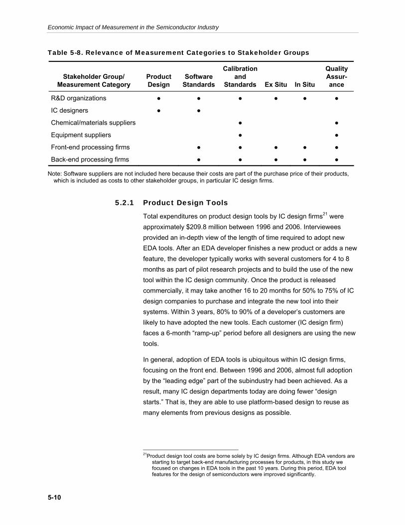
Economic Impact of Measurement in the Semiconductor Industry
Table 5-8. Relevance of Measurement Categories to Stakeholder Groups
Calibration Quality Stakeholder Group/ Product Software and Assur-
Measurement Category Design Standards Standards Ex Situ In Situ ance
R&D organizations ● ● ● ● ● ●
IC designers ● ●
Chemical/materials suppliers ● ●
Equipment suppliers ● ●
Front-end processing firms ● ● ● ● ●
Back-end processing firms ● ● ● ● ●
Note: Software suppliers are not included here because their costs are part of the purchase price of their products, which is included as costs to other stakeholder groups, in particular IC design firms.
5.2.1 Product Design Tools
Total expenditures on product design tools by IC design firms21 were approximately $209.8 million between 1996 and 2006. Interviewees provided an in-depth view of the length of time required to adopt new EDA tools. After an EDA developer finishes a new product or adds a new feature, the developer typically works with several customers for 4 to 8 months as part of pilot research projects and to build the use of the new tool within the IC design community. Once the product is released commercially, it may take another 16 to 20 months for 50% to 75% of IC design companies to purchase and integrate the new tool into their systems. Within 3 years, 80% to 90% of a developer’s customers are likely to have adopted the new tools. Each customer (IC design firm) faces a 6-month “ramp-up” period before all designers are using the new tools.
In general, adoption of EDA tools is ubiquitous within IC design firms, focusing on the front end. Between 1996 and 2006, almost full adoption by the “leading edge” part of the subindustry had been achieved. As a result, many IC design departments today are doing fewer “design starts.” That is, they are able to use platform-based design to reuse as many elements from previous designs as possible.
21Product design tool costs are borne solely by IC design firms. Although EDA vendors are starting to target back-end manufacturing processes for products, in this study we focused on changes in EDA tools in the past 10 years. During this period, EDA tool features for the design of semiconductors were improved significantly.
5-10
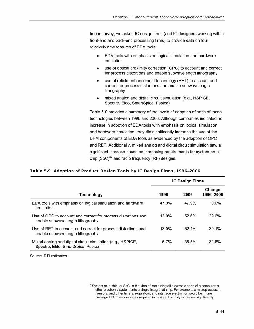
Chapter 5 — Measurement Technology Adoption and Expenditures
In our survey, we asked IC design firms (and IC designers working within front-end and back-end processing firms) to provide data on four relatively new features of EDA tools:
• EDA tools with emphasis on logical simulation and hardware emulation
• use of optical proximity correction (OPC) to account and correct for process distortions and enable subwavelength lithography
• use of reticle-enhancement technology (RET) to account and correct for process distortions and enable subwavelength lithography
• mixed analog and digital circuit simulation (e.g., HSPICE, Spectre, Eldo, SmartSpice, Pspice)
Table 5-9 provides a summary of the levels of adoption of each of these technologies between 1996 and 2006. Although companies indicated no increase in adoption of EDA tools with emphasis on logical simulation and hardware emulation, they did significantly increase the use of the DFM components of EDA tools as evidenced by the adoption of OPC and RET. Additionally, mixed analog and digital circuit simulation saw a significant increase based on increasing requirements for system-on-a-chip (SoC)22 and radio frequency (RF) designs.
Table 5-9. Adoption of Product Design Tools by IC Design Firms, 1996–2006
IC Design Firms
Change Technology 1996 2006 1996–2006
EDA tools with emphasis on logical simulation and hardware emulation
Use of OPC to account and correct for process distortions and enable subwavelength lithography
Use of RET to account and correct for process distortions and enable subwavelength lithography
Mixed analog and digital circuit simulation (e.g., HSPICE, Spectre, Eldo, SmartSpice, Pspice
Source: RTI estimates.
47.9% 47.9% 0.0%
13.0% 52.6% 39.6%
13.0% 52.1% 39.1%
5.7% 38.5% 32.8%
22System on a chip, or SoC, is the idea of combining all electronic parts of a computer or other electronic system onto a single integrated chip. For example, a microprocessor, memory, and other timers, regulators, and interface electronics would be in one packaged IC. The complexity required in design obviously increases significantly.
5-11
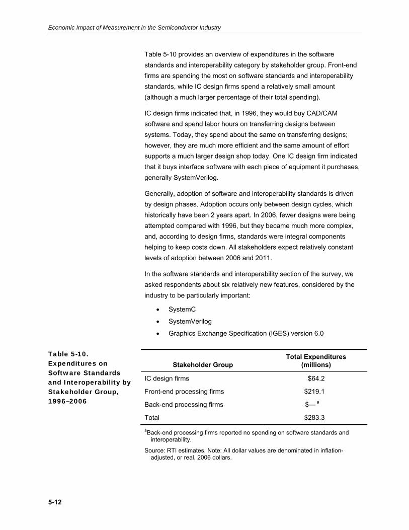
Economic Impact of Measurement in the Semiconductor Industry
Table 5-10 provides an overview of expenditures in the software standards and interoperability category by stakeholder group. Front-end firms are spending the most on software standards and interoperability standards, while IC design firms spend a relatively small amount (although a much larger percentage of their total spending).
IC design firms indicated that, in 1996, they would buy CAD/CAM software and spend labor hours on transferring designs between systems. Today, they spend about the same on transferring designs; however, they are much more efficient and the same amount of effort supports a much larger design shop today. One IC design firm indicated that it buys interface software with each piece of equipment it purchases, generally SystemVerilog.
Generally, adoption of software and interoperability standards is driven by design phases. Adoption occurs only between design cycles, which historically have been 2 years apart. In 2006, fewer designs were being attempted compared with 1996, but they became much more complex, and, according to design firms, standards were integral components helping to keep costs down. All stakeholders expect relatively constant levels of adoption between 2006 and 2011.
In the software standards and interoperability section of the survey, we asked respondents about six relatively new features, considered by the industry to be particularly important:
• SystemC
• SystemVerilog
• Graphics Exchange Specification (IGES) version 6.0
Table 5-10. Expenditures on Software Standards and Interoperability by
Stakeholder Group
IC design firms
Total Expenditures (millions)
$64.2
Stakeholder Group, 1996–2006
Front-end processing firms
Back-end processing firms
$219.1
$— a
Total $283.3
aBack-end processing firms reported no spending on software standards and interoperability.
Source: RTI estimates. Note: All dollar values are denominated in inflation-adjusted, or real, 2006 dollars.
5-12
Chapter 5 — Measurement Technology Adoption and Expenditures
• Standard for the Exchange of Product Model Data (STEP)
• Graphic Data System (GDSII, GDSIII & GDSIV)
• Open Artwork Systems Interchange Standard (OASIS)
SystemC was pushed as a new modeling language standard beginning in 1999, and, according to EDA vendors, the industry was been standardized around SystemC since around the year 2000. In 2006, interviews suggest that approximately 75% to 80% of system architects use SystemC.
SystemVerilog is an extension of Verilog, a set of verification and implementation tools that have been gradually built up by various groups (i.e., for over 10 years).23 One design firm noted that SystemVerilog is the de facto standard for providing a higher level of abstraction (known as “above RTL”), and that before SystemVerilog, standardization was sorely lacking in this area. One EDA designer estimated that 50% of the relevant players in the industry are using SystemVerilog.
IGES is not widely used in the semiconductor industry, but it is the predominant computer-aided design (CAD)-related standard in the semiconductor industry. There is little adoption of STEP. Several companies indicated that they planned to move to STEP in the future, but only when the industry moved as a whole.
We were able to get adoption estimates on GDS use. Table 5-11 provides the relative levels of adoption of IC designers, front-end firms, and back-end firms. IC designers have virtually fully adopted some version of GDS, whereas front-end and back-end firms have not. Several firms indicated that they plan to move toward OASIS in the next several years, but they were not using it currently.
5.2.2 Calibration and Standard Test Methods
Although calibration and standard test methods do not constitute a large cost compared with other categories, the expenses can be significant. Table 5-12 provides an overview of costs in this category by stakeholder group.
Interview results suggest that many companies are not using calibration and standard test methods because (1) they are requiring suppliers to do this for them and (2) such activities are becoming more automated and in many cases assumed to be part of QA processes.
23This new version adds new capabilities to Verilog making coding faster and generally making systems more compact.
5-13
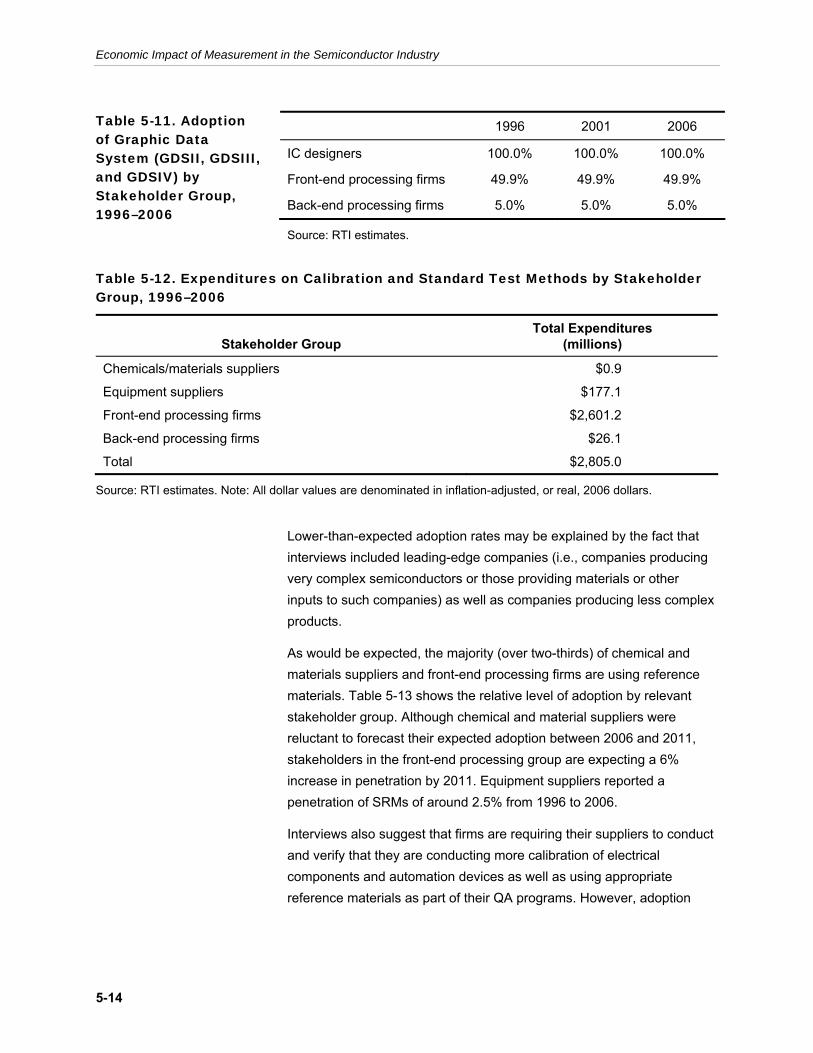
Economic Impact of Measurement in the Semiconductor Industry
Table 5-11. Adoption 1996 2001 2006 of Graphic Data System (GDSII, GDSIII, IC designers 100.0% 100.0% 100.0%
and GDSIV) by Front-end processing firms 49.9% 49.9% 49.9% Stakeholder Group, 1996–2006
Back-end processing firms 5.0% 5.0% 5.0%
Source: RTI estimates.
Table 5-12. Expenditures on Calibration and Standard Test Methods by Stakeholder Group, 1996–2006
Total Expenditures Stakeholder Group (millions)
Chemicals/materials suppliers $0.9
Equipment suppliers $177.1
Front-end processing firms $2,601.2
Back-end processing firms $26.1
Total $2,805.0
Source: RTI estimates. Note: All dollar values are denominated in inflation-adjusted, or real, 2006 dollars.
Lower-than-expected adoption rates may be explained by the fact that interviews included leading-edge companies (i.e., companies producing very complex semiconductors or those providing materials or other inputs to such companies) as well as companies producing less complex products.
As would be expected, the majority (over two-thirds) of chemical and materials suppliers and front-end processing firms are using reference materials. Table 5-13 shows the relative level of adoption by relevant stakeholder group. Although chemical and material suppliers were reluctant to forecast their expected adoption between 2006 and 2011, stakeholders in the front-end processing group are expecting a 6% increase in penetration by 2011. Equipment suppliers reported a penetration of SRMs of around 2.5% from 1996 to 2006.
Interviews also suggest that firms are requiring their suppliers to conduct and verify that they are conducting more calibration of electrical components and automation devices as well as using appropriate reference materials as part of their QA programs. However, adoption
5-14
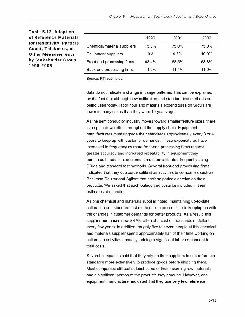
Chapter 5 — Measurement Technology Adoption and Expenditures
Table 5-13. Adoption of Reference Materials 1996 2001 2006 for Resistivity, Particle Count, Thickness, or Chemical/material suppliers 75.0% 75.0% 75.0%
Other Measurements Equipment suppliers 9.3 9.6% 10.0% by Stakeholder Group, 1996–2006
Front-end processing firms 68.4% 68.5% 68.8%
Back-end processing firms 11.2% 11.4% 11.9%
Source: RTI estimates.
data do not indicate a change in usage patterns. This can be explained by the fact that although new calibration and standard test methods are being used today, labor hour and materials expenditures on SRMs are lower in many cases than they were 10 years ago.
As the semiconductor industry moves toward smaller feature sizes, there is a ripple-down effect throughout the supply chain. Equipment manufacturers must upgrade their standards approximately every 3 or 4 years to keep up with customer demands. These expenditures have increased in frequency as more front-end processing firms request greater accuracy and increased repeatability in equipment they purchase. In addition, equipment must be calibrated frequently using SRMs and standard test methods. Several front-end processing firms indicated that they outsource calibration activities to companies such as Beckman Coulter and Agilent that perform periodic service on their products. We asked that such outsourced costs be included in their estimates of spending.
As one chemical and materials supplier noted, maintaining up-to-date calibration and standard test methods is a prerequisite to keeping up with the changes in customer demands for better products. As a result, this supplier purchases new SRMs, often at a cost of thousands of dollars, every few years. In addition, roughly five to seven people at this chemical and materials supplier spend approximately half of their time working on calibration activities annually, adding a significant labor component to total costs.
Several companies said that they rely on their suppliers to use reference standards more extensively to produce goods before shipping them. Most companies still test at least some of their incoming raw materials and a significant portion of the products they produce. However, one equipment manufacturer indicated that they use very few reference
5-15

Economic Impact of Measurement in the Semiconductor Industry
materials, instead relying on the use of such by their suppliers. Before 1990, the same company used NIST-calibrated electrical components, but now they outsource such measurements.
5.2.3 Ex Situ Process Control
Table 5-14 provides an overview of costs in this category by stakeholder group. As noted in Chapter 3, a major trend has been the shift in analytical capabilities from ex situ tools in centralized laboratories to in situ measurements within the on-line fabrication equipment itself. Such a development would reasonably reduce the expenditures on ex situ tools in favor of in situ tools.
For leading-edge manufacturers, one-time investments in equipment occur based on technology changes in the size of the wafer or linewidth or changes to the material being used. Other firms adopt new technologies to save money when budgets allow. Interviews found that many firms are
• outsourcing several infrequent measurement activities to focused analytical laboratories,
• centralizing laboratories where they conduct certain measurements that require particularly expensive equipment and highly skilled and experienced staff, and/or
• fully using the features of existing equipment and adding new features before purchasing new equipment.
For example, one manufacturing firm said that they outsourced transmission electron microscopy (TEM) because it was too expensive and they only needed five to ten measurements per year. And they did not inspect incoming wafers because they trusted their suppliers. Another firm suggested that they might move their mask measurement activities (e.g., optical microscopy and SEM) offshore to save money.
Table 5-14. Expenditures on Ex Situ Process Control by Stakeholder Group, 1996– 2006
Total Expenditures Stakeholder Group (millions)
Front-end processing firms $196.5
Back-end processing firms $473.6
Total $670.1
Source: RTI estimates. Note: All dollar values are denominated in inflation-adjusted, or real, 2006 dollars.
5-16

Chapter 5 — Measurement Technology Adoption and Expenditures
Further, the relationship between design activities and production continues to change, causing estimation of ex situ costs to be difficult.24
According to one manufacturer, measurement technology was only 10% of the cost of a tool used in a wafer fabrication facility operating with technologies at 0.8- or 0.5-micron linewidths, which is considered outdated technology by leading-edge manufacturers. The measurement cost rises to 30% of the cost of a “tool” used in a wafer fabrication at 110-nm linewidth today. This manufacturer estimated that at 60 nm the cost of measurement might be as high as 35% of the cost of the tool.
The move to single-wafer processing from 25-wafer “batch processing” techniques used in 1996 was necessary to produce high-quality products at smaller sizes. However, this change caused throughput to decrease significantly and thus forced companies to purchase more equipment to compensate. One front-end processor said that he doubled the number of etchers he had because of this change. Ex situ measurement equipment and work associated with such also had to be increased.
Within the semiconductor supply chain, only front-end and back-end processing firms use ex situ equipment. Over the past decade, the adoption of new ex situ equipment has proceeded gradually with the most leading-edge manufacturers purchasing products that can measure more precisely and to smaller dimensions and the less advanced manufacturers following behind them, in some cases even purchasing used equipment from the leading companies.
Study participants provided their level of adoption of several key ex situ technologies within five categories:
• mask measurement
• CD measurement
• overlay measurement
• wafer inspection and defect review
• thin-film metrology
Table 5-15 shows the trends in adoption of each technology by front-end processing and back-end processing firms. Back-end firms tend to lag
24There are many large and small firms that have design activities, front-end processing, and back-end processing under the same roof (literally or in terms of company structure). However, in many cases, these three activities take place in separate organizations. Fabless manufacturers commonly design chips and have a contract manufacturing organization (CMO) produce their product that then bears the name of the designer. We only spoke to one CMO; thus, our ex situ costs may not accurately reflect their adoption and investment activities.
5-17
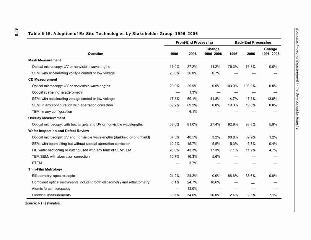
Table 5-15. Adoption of Ex Situ Technologies by Stakeholder Group, 1996–2006
Front-End Processing Back-End Processing
Change Change Question 1996 2006 1996–2006 1996 2006 1996–2006
Mask Measurement
Optical microscopy: UV or nonvisible wavelengths 16.0% 27.2% 11.2% 76.3% 76.3% 0.0%
SEM: with accelerating voltage control or low voltage 26.6% 26.0% −0.7% — — —
CD Measurement
Optical microscopy: UV or nonvisible wavelengths 29.9% 29.9% 0.0% 100.0% 100.0% 0.0%
Optical scattering: scatterometry — 1.3% — — — —
SEM: with accelerating voltage control or low voltage 17.3% 59.1% 41.8% 4.7% 17.8% 13.0%
SEM: in any configuration with aberration correction 69.2% 69.2% 0.0% 19.0% 19.0% 0.0%
TEM: in any configuration — 6.1% — — — —
Overlay Measurement
Optical microscopy: with box targets and UV or nonvisible wavelengths 53.6% 81.0% 27.4% 92.9% 98.8% 5.9%
Wafer Inspection and Defect Review
Optical microscopy: UV and nonvisible wavelengths (darkfield or brightfield) 37.3% 40.5% 3.2% 88.8% 89.9% 1.2%
SEM: with beam tilting but without special aberration correction 10.2% 15.7% 5.5% 5.3% 5.7% 0.4%
FIB wafer sectioning or cutting used with any form of SEM/TEM 26.0% 43.3% 17.3% 7.1% 11.9% 4.7%
TEM/SEM: with aberration correction 10.7% 16.3% 5.6% — — —
STEM — 3.7% — — — —
Thin-Film Metrology
Ellipsometry: spectroscopic 24.2% 24.2% 0.0% 88.6% 88.6% 0.0%
Combined optical instruments including both ellipsometry and reflectometry 6.1% 24.7% 18.6% — — —
Atomic force microscopy — 13.0% — — — —
Electrical measurements 8.6% 34.6% 26.0% 2.4% 9.5% 7.1%
Econom
ic Impact of M
easurement in the S
emiconductor Industry
Source: RTI estimates.
5-18
Chapter 5 — Measurement Technology Adoption and Expenditures
behind front-end firms in adopting new technologies because they often do not need to make measurements nearly as small as those required in front-end plants.
Mask Measurement
In the mask measurement category, front-end firms increased their adoption of optical microscopy. Optical microscopy provides a strong advantage in rapid throughput, because with an optical microscope no time-consuming evacuation of the sample chamber is required to place the sample in high vacuum. Advances in short-wavelength high-resolution immersion microscopes seem to have kept pace with the reduction in size of mask features, motivating an increase in adoption of optical microscopy. Respondents indicated that “environmental” or “high-pressure” SEM tools have not yet been widely adopted in the semiconductor industry, despite predictions that such instruments would be superior in reducing image faults because of electrostatic charging of the mask surface. Apparently, SEMs with accelerating voltage control have been adequately successful in providing the needed images along with superior maintainability.
CD Measurement
Within this category, SEM with accelerating voltage control or low voltage saw a large increase in adoption by front-end processing firms, from approximately 17% in 1996 to 59% in 2006. Back-end firms also increased their adoption of this technology by 13% to approximately 18% adoption in 2006. According to our interviews, most of this change occurred between 1996 and 2001. Optical microscopy was adequate for the resolution demands of 1996; however, by 2006, scanning electron microscopy was increasingly required to resolve the smaller features being produced at that time.
The survey results indicate some confusion of terminology: SEM with aberration control was adopted by 69% of companies in 1996 according to the respondents, while manufacturers of electron microscopes indicate that no significant commercial versions of aberration-corrected electron microscopes were available for sale in 1996. For example, a JEOL aberration-corrected TEM was only delivered to Oxford University in 2004. Some confusion may have resulted because astigmatism correction, which was developed for electron microscopes in 1947, is sometimes considered a form of aberration correction.
5-19

Economic Impact of Measurement in the Semiconductor Industry
5.2.4
Overlay Measurement
Within the overlay measurement category, optical microscopy with box targets and UV or nonvisible wavelengths saw an increase in adoption from 54% to 81% by front-end firms. Back-end firms increased almost 6%, with 2006 adoption estimated to be 99%. According to our interviews, most of this adoption occurred between 2001 and 2006. Improvements in UV light sources and imaging technology (such as UV-sensitive digital cameras) allowed short-wavelength optical microscopes to keep pace with increasing resolution demands of overlay measurements.
Wafer Inspection and Defect Review
Within this category, FIB wafer sectioning or cutting used with any form of SEM/TEM saw the largest increase in adoption by front-end firms— 17% change (43% in 2006)—and also saw slight increases by back-end firms—5% change (12% in 2006). Dual-beam FIB instruments including SEM/EDS were mentioned in the 1995 NTRS as a new technology available for defect analysis for defect studies. FIB preparation of sections from wafers offers extremely high accuracy and very rapid throughput compared with the manual methods that preceded its development. Adoption is a strong economic advantage despite the relatively high capital cost of a FIB instrument. The 2001 ITRS noted that lift-out preparation of cross sections by FIB was starting to become possible for observation of defects by TEM or scanning-transmission electron microscopy (STEM). This is consistent with the finding of the survey of a large increase in use of FIB between 1996 and 2006.
Thin-Film Metrology
Within the thin-film metrology category, although elipsometry saw no change in adoption, there was significant adoption of combined optical instruments including both ellipsometry and reflectometry (19% change up to 25% in 2006) by front-end firms. Back-end firms did not adopt this technology in 1996 or 2006. Also, electrical measurement for thin-film measurement saw a 26% increase, up to approximately 35% in 2006, for front-end firms and a 7% increase, up to 10%, by back-end firms.
In Situ Process Control
Table 5-16 provides an overview of costs in this category by stakeholder group as well as the percentage change. As noted in Chapter 3, a major advantage of in situ measurement is that a production process can be
5-20

2006
Chapter 5 — Measurement Technology Adoption and Expenditures
Table 5-16. Expenditures on In Situ Process Control by Stakeholder Group, 1996–
Total Expenditures Stakeholder Group (millions)
Front-end processing firms $1,346.5
Back-end processing firms $1,082.2
Total $2,428.7
aBack-end processing firms reported $0 in expenditures in 1996 and almost $500 million in 2006. Thus, the percentage change is not an appropriate metric.
Source: RTI estimates. Note: All dollar values are denominated in inflation-adjusted, or real, 2006 dollars.
actively controlled while it is under way. Active control improves process repeatability and provides real-time feedback on manufacturing processes. This feedback is essential to controlling scrap rates and rework costs, especially as device features continue to shrink.
Adoption of in situ process control equipment and processes has occurred as companies see the cost savings and quality improvement benefits involved in taking real-time measurements of products and process steps and making immediate adjustments accordingly. According to our survey respondents, although some companies have made investments directly aimed at integrating in situ capabilities, others have merely begun to receive some amount of in situ technology that is now being included with new process control equipment. We asked that they estimate all in situ costs, including those subsumed in the cost of equipment.
In 1996, in situ process control was only being used by the most advanced manufacturing companies, but between 1996 and 2006, a large share of front-end and back-end processing firms adopted many types of in situ technologies. Some were willing to spend money to get new features, such as the capability for real-time process adjustments, while others gained new in situ features as part of their standard equipment upgrade cycles.
Adoption of in situ technologies is also related to the move to single-wafer manufacturing from batch manufacturing. This change caused the industry to look for ways to increase throughput, and in situ technologies furthered that objective.
5-21
Economic Impact of Measurement in the Semiconductor Industry
In our survey, we asked respondents about their level of adoption of several key in situ technologies and pieces of in situ equipment within three categories:
• processing parameters and process vacuum monitoring
• off-wafer, in situ deposition monitoring
• on-wafer deposition monitoring and endpoint detection
Table 5-17 shows the level of adoption of specific technologies within each of these categories.
Processing Parameters and Process Vacuum Monitoring
Front-end processors increased their adoption of digital process control (DPC) from 8% to 34% in 2006, and back-end processors increased their adoption from 48% to 63% in 2006. According to our interviews, most of this adoption occurred between 1996 and 2001. Advanced process control (APC), in which data from an array of tools are integrated into a fab-wide network, saw a less extreme increase in adoption by front-end firms (5 percentage point increase), although back-end firms increased to approximately 27% from virtually no adoption in 1996.
No changes were reported in adoption of crystal oscillator film thickness monitors. These monitors are well-established and cost-effective sensors that were introduced into vacuum process technology long before the initial period of this study. Therefore, we would anticipate little change in adoption rates.
Off-Wafer, In Situ Deposition Monitoring
No changes were reported in adoption of crystal oscillator film thickness monitors. These monitors are well-established and cost-effective sensors that were introduced into vacuum process technology decades ago, long before the initial period of this study. Therefore, it would be anticipated that there would be little change in rates of adoption. With these sensors, material is deposited on a piezoelectric crystal, and the change in the resonant frequency is measured to indicate the mass of material, and therefore the thickness, that has been deposited. Because frequencies can be measured with great precision, these sensors have adequate sensitivity to measure thin films. However, measuring frequency is an indirect measurement of thickness, and measuring on the surface of the crystal is not the same as directly measuring on the surface of the wafer,
5-22
Table 5-17. Adoption of In Situ Technologies by Stakeholder Group, 1996–2006
Front-End Processing Back-End Processing
Change Change Question 1996 2006 1996–2006 1996 2006 1996–2006
Processing Parameters and Process Vacuum Monitoring
Digital process control, in which gauges and sensors for process 26.2% 34.3% 8.1% 15.0% 63.1% 48.1% state parameters (e.g., vacuum, time, temperature) are integrated into a digital controller on the processing tool
Advanced process control, in which individual controllers provide 26.1% 31.5% 5.4% – 26.7% – data on process state parameters to a central, fab-wide system
Residual gas analyzers 20.8% 20.8% 0.0% – 3.8% –
Off-Wafer, In Situ Deposition Monitoring
Crystal oscillator film thickness monitor 15.4% 15.4% 0.0% 23.7% 23.7% 0.0%
On-Wafer, Deposition Monitoring, and Endpoint Detection
Optical emission spectroscopy for etch endpoint detection 34.8% 51.0% 16.1% 8.3% 49.8% 41.5%
Optical reflectivity measurement for deposition and CMP endpoint 18.2% 18.2% 0.0% – - – detection
Optical interferometry, including infrared backside CMP process 18.2% 39.1% 20.9% – - – monitoring
Optical ellipsometry for thickness monitoring 29.5% 35.6% 6.1% – 38.1% –
Source: RTI estimates.
Chapter 5 —
Measurem
ent Technology Adoption and E
xpenditures
5-23
Economic Impact of Measurement in the Semiconductor Industry
For these reasons, the use of optical on-wafer techniques has grown while the adoption of off-wafer techniques has remained static.
On-Wafer Deposition Monitoring and Endpoint Detection
In this category, several technologies saw increases in adoption. Optical emission spectroscopy for etch endpoint detection increased by 16% (to 51% in 2006) for front-end firms, while back-end firms’ adoption increased 42% (to almost 50% in 2006). Our interviews suggested that most of this adoption occurred between 1996 and 2001.
Optical interferometry saw a 21% increase by front-end firms (to 39% in 2006), and optical elipsometry for thickness monitoring saw a 6% increase by front-end firms and a 38% increase by back-end firms. According to several equipment manufacturers, optical interferometry was a major investment between 1996 and 2006. Although our survey data do not reflect his opinion, one equipment manufacturer stated that in 1996 optical interferometry was used by less than 5% of the industry, while today he estimated that approximately three-fourths of front-end processing firms use it.
Residual gas analyzers are well-established instruments that have been used for years to monitor conditions within vacuum systems. They can be used both for process control and for leak detection and diagnosis. As confirmed by the survey data, one would expect the use of such workhorse instruments to be relatively stable over time. Because residual gas analyzers function as mass spectrometers, they typically detect elements and small molecular fragments. Thus, they are not generally used to make positive identifications of specific organic gases.
In contrast, Fourier transform infrared (FTIR) gas monitors, which use Fourier transform infrared spectroscopy as a detection method, are capable of identifying specific molecules from their spectroscopic signature. It was expected that FTIR gas monitors, which are currently available from major process control suppliers, would have been adopted by the semiconductor industry in recent years. Survey results suggest that the large-scale adoption of FTIR gas monitors has not been required by current demands of the industry and that residual gas analyzers continue to perform satisfactorily.
5-24

Chapter 5 — Measurement Technology Adoption and Expenditures
5.2.5 Quality Assurance
Table 5-18 provides an overview of costs in this category by stakeholder group. Several front-end processing firms with which we spoke had large quality departments of 50 or more staff members who focused on testing and addressing quality issues at the beginning and end of their process. Alternatively, several companies mentioned outsourcing measurements such as wafer purity.
Anecdotally, one chemical and material supplier with whom we spoke indicated that his company spends approximately 20% to 25% of the company’s revenue on QA. However, when his comment was probed further, it became apparent that he viewed many measurements in the production environment as QA even though the activities were the use of “calibration and standard test methods” by our definition. This was a common issue that we addressed in our cost calculations.25
Our interviews suggest that QA measurement is increasing largely based on the shift to 300-mm wafers from 200-mm wafers, an older, less complex technology. One firm mentioned that they supply many semiconductors to the automotive industry and that automotive companies require extensive QA testing. They have to follow International Standards Organization (ISO) standards and are audited
Table 5-18. Expenditures on Quality Assurance Techniques by Stakeholder Group, 1996–2006
Total Expenditures Stakeholder Group (millions)
Chemical/materials suppliers $27.5
Equipment suppliers $43.3
Front-end processing firms $2,265.4
Back-end processing firms $402.2
Total $2,738.3
Source: RTI estimates. Note: All dollar values are denominated in inflation-adjusted, or real, 2006 dollars.
25The difference between QA and other process control and calibration measurements for this survey was explicitly described to all survey respondents, although some may not have been able to accurately differentiate their spending. As defined in Section 3.7, for this study “QA” was defined as the methods manufacturers and suppliers use to ensure that their finished products meet their customers’ specifications. QA differs from process control, which monitors manufacturing conditions at individual process operations. The intent of QA is to certify a product or material prior to providing it to the next stage in the value chain, as well as to perform testing of incoming materials.
5-25

Economic Impact of Measurement in the Semiconductor Industry
every 6 months. As in other categories, several firms discussed outsourcing some of their QA activities.
New QA techniques have been adopted steadily over the past several years as new technologies have been introduced into the wafer fabrication process. QA usually refers to the examination of products before shipment rather than an examination of raw materials upon receipt. As discussed, many front-end suppliers are providing more QA services for their customers; several suppliers interviewed indicated that they provide a certification of analysis for each incoming chemical shipment and no further validation is required by the end user (i.e., a wafer fab).
In our survey, we asked respondents about their level of adoption of several key QA techniques and pieces of equipment within five categories:
• advanced QA techniques to measure bare wafer properties including Si, epi, and new wafer chemistries (e.g., SiGe, InP, Soi)
• higher accuracy analytical tools to measure the purity of chemical products used in semiconductor manufacturing
• electrical testing of equipment, assemblies, wafers, or other products
• size, dimension, and defect monitoring
• increased automation for end-of-line wafer probe stations and test fixtures to improve throughputs
Table 5-19 shows the level of adoption of all technologies and techniques asked about in the survey. Not surprisingly, chemical and materials suppliers have very high levels of adoption in this category.
Survey data show close to full adoption of advanced QA techniques such as wafer bow, wafer purity, particulates on wafer surface, and wafer crystallography. Equipment suppliers show a very high level of adoption specifically for techniques to test particulates on the wafer surface (75%). Front-end firms are increasing their adoption of all of these techniques, and some back-end firms are testing particulates on wafer surfaces. Although there was little change between 1996 and 2006, there was a high level of adoption by two major supplier groups—chemical/materials suppliers (100%) and equipment suppliers (75%). A variety of chemicals are used in modern semiconductor manufacturing, including gases (e.g., H2, O2, SiH4), liquids (e.g., etchants, bases, acids, and buffered solutions), and solids (e.g., metals and Si wafers). Between 1996 and
5-26
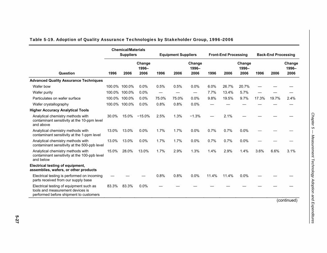
Table 5-19. Adoption of Quality Assurance Technologies by Stakeholder Group, 1996–2006
Chemical/Materials Suppliers Equipment Suppliers Front-End Processing Back-End Processing
Change 1996–
Change 1996–
Change 1996–
Change 1996–
Question 1996 2006 2006 1996 2006 2006 1996 2006 2006 1996 2006 2006
Advanced Quality Assurance Techniques Wafer bow 100.0% 100.0% 0.0% 0.5% 0.5% 0.0% 6.0% 26.7% 20.7% — — — Wafer purity 100.0% 100.0% 0.0% — — — 7.7% 13.4% 5.7% — — — Particulates on wafer surface 100.0% 100.0% 0.0% 75.0% 75.0% 0.0% 9.8% 19.5% 9.7% 17.3% 19.7% 2.4% Wafer crystallography 100.0% 100.0% 0.0% 0.8% 0.8% 0.0% — — — — — —
Higher Accuracy Analytical Tools Analytical chemistry methods with contaminant sensitivity at the 10-ppm level and above
30.0% 15.0% −15.0% 2.5% 1.3% −1.3% — 2.1% — — — —
Analytical chemistry methods with contaminant sensitivity at the 1-ppm level
13.0% 13.0% 0.0% 1.7% 1.7% 0.0% 0.7% 0.7% 0.0% — — —
Analytical chemistry methods with contaminant sensitivity at the 500-ppb level
13.0% 13.0% 0.0% 1.7% 1.7% 0.0% 0.7% 0.7% 0.0% — — —
Analytical chemistry methods with contaminant sensitivity at the 100-ppb level and below
15.0% 28.0% 13.0% 1.7% 2.9% 1.3% 1.4% 2.9% 1.4% 3.6% 6.6% 3.1%
Electrical testing of equipment, assemblies, wafers, or other products
Electrical testing is performed on incoming parts received from our supply base
— — — 0.8% 0.8% 0.0% 11.4% 11.4% 0.0% — — —
Electrical testing of equipment such as tools and measurement devices is performed before shipment to customers
83.3% 83.3% 0.0% — — — — — — — — —
(continued)
Chapter 5 —
Measurem
ent Technology Adoption and E
xpenditures
5-27
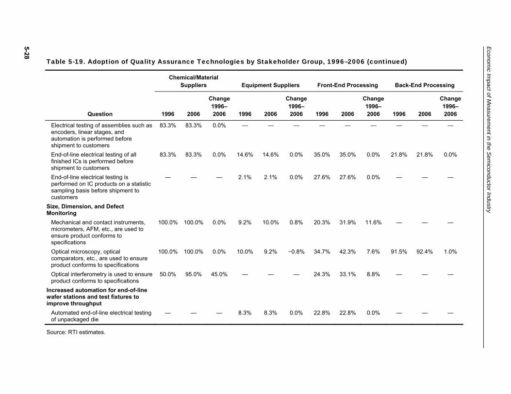
Table 5-19. Adoption of Quality Assurance Technologies by Stakeholder Group, 1996–2006 (continued)
Chemical/Material Suppliers Equipment Suppliers Front-End Processing Back-End Processing
Change Change Change Change 1996– 1996– 1996– 1996–
Question 1996 2006 2006 1996 2006 2006 1996 2006 2006 1996 2006 2006
Electrical testing of assemblies such as 83.3% 83.3% 0.0% — — — — — — — — — encoders, linear stages, and automation is performed before shipment to customers End-of-line electrical testing of all 83.3% 83.3% 0.0% 14.6% 14.6% 0.0% 35.0% 35.0% 0.0% 21.8% 21.8% 0.0% finished ICs is performed before shipment to customers End-of-line electrical testing is — — — 2.1% 2.1% 0.0% 27.6% 27.6% 0.0% — — — performed on IC products on a statistic sampling basis before shipment to customers
Size, Dimension, and Defect Monitoring
Mechanical and contact instruments, 100.0% 100.0% 0.0% 9.2% 10.0% 0.8% 20.3% 31.9% 11.6% — — — micrometers, AFM, etc., are used to ensure product conforms to specifications Optical microscopy, optical 100.0% 100.0% 0.0% 10.0% 9.2% −0.8% 34.7% 42.3% 7.6% 91.5% 92.4% 1.0% comparators, etc., are used to ensure product conforms to specifications Optical interferometry is used to ensure 50.0% 95.0% 45.0% — — — 24.3% 33.1% 8.8% — — — product conforms to specifications
Increased automation for end-of-line wafer stations and test fixtures to improve throughput
Automated end-of-line electrical testing — — — 8.3% 8.3% 0.0% 22.8% 22.8% 0.0% — — — of unpackaged die
Econom
ic Impact of M
easurement in the S
emiconductor Industry
Source: RTI estimates.
5-28
Chapter 5 — Measurement Technology Adoption and Expenditures
2006, the introduction of new materials into semiconductor fabrication has meant that the chemical manufacturer has to perform new QA tests before shipment to the wafer fabrication. In addition, the constant reduction in feature size during this period has placed greater demands on the properties of common starting materials, and the specifications developed by the industry have placed greater demands on controlling composition, moisture content, and other material properties.
A look at the evolution of materials standards published by SEMI reinforces the drive toward higher purity chemical use in wafer fabrication. The evolution of the semiconductor industry between 1996 and 2006 increased the level of scrutiny that process chemicals undergo prior to shipment to front-end processors. The purity of process gases is usually certified using mass spectrometry and other methods to ensure that impurities are within acceptable levels, and purity requirements have increased significantly during this period. Water is a common impurity, and moisture levels have been notably reduced during the past 10 years. Likewise, the purity of liquid chemicals is often checked using liquid chromatography or atomic absorption measurements. Finally, the purity of metals, such as sputter cathodes used during wafer fabrication, must also be certified with high accuracy using methods such as atomic absorption.
Consequently, for the higher accuracy analytical tools category, chemical and materials suppliers who work with analytical chemistry methods are moving from containment sensitivity at the 10-ppm level and above to the 100-ppm level and below. Because the end users (i.e., front-end processing and back-end processing firms) require a certificate of chemical purity with each shipment instead of performing incoming quality verifications, no other stakeholder groups have significant adoption in this subcategory.
At back-end sites, QA methods have emphasized higher throughput and the ability to measure smaller defects. A variety of electrical tests are usually performed during back-end QA operations, usually on a sampling basis. As IC packaging has migrated from large flat pins used on quad flat packs to round solder spheres (e.g., flip chip and ball grid arrays) and small leads (e.g., high-density interconnects), the nature of electrical testing has also changed. Fixtures have become more advanced to accommodate the myriad packaging options and higher pin counts that began to emerge around 1995, and technologies that provide a constant connection force are desired.
5-29

Economic Impact of Measurement in the Semiconductor Industry
In the electrical testing category, chemical and materials suppliers have a very high adoption (over 80%) of electrical testing procedures, although this did not change much over the past 10 years. Equipment suppliers do some end-of-line electrical testing of ICs (15%), and front-end and back-end firms do more (35% and 22% respectively), although, again, there was no change between 1996 and 2006.
5-30
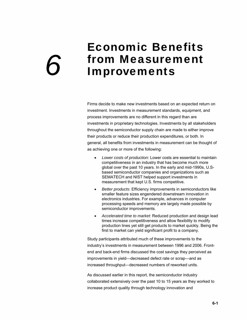
6Economic Benefits from Measurement
Improvements
Firms decide to make new investments based on an expected return on investment. Investments in measurement standards, equipment, and process improvements are no different in this regard than are investments in proprietary technologies. Investments by all stakeholders throughout the semiconductor supply chain are made to either improve their products or reduce their production expenditures, or both. In general, all benefits from investments in measurement can be thought of as achieving one or more of the following:
• Lower costs of production: Lower costs are essential to maintain competitiveness in an industry that has become much more global over the past 10 years. In the early and mid-1990s, U.S-based semiconductor companies and organizations such as SEMATECH and NIST helped support investments in measurement that kept U.S. firms competitive.
• Better products: Efficiency improvements in semiconductors like smaller feature sizes engendered downstream innovation in electronics industries. For example, advances in computer processing speeds and memory are largely made possible by semiconductor improvements.
• Accelerated time to market: Reduced production and design lead times increase competitiveness and allow flexibility to modify production lines yet still get products to market quickly. Being the first to market can yield significant profit to a company.
Study participants attributed much of these improvements to the industry’s investments in measurement between 1996 and 2006. Front-end and back-end firms discussed the cost savings they perceived as improvements in yield—decreased defect rate or scrap—and as increased throughput—decreased numbers of reworked units.
As discussed earlier in this report, the semiconductor industry collaborated extensively over the past 10 to 15 years as they worked to increase product quality through technology innovation and
6-1
Economic Impact of Measurement in the Semiconductor Industry
standardization. In the case of suppliers—chemical and materials suppliers, equipment suppliers, and IC design firms—the primary impetus to invest in measurement improvement was to deliver on commitments made to front-end and back-end processors whose product designs required suppliers to deliver on exacting product specifications. Suppliers stated that they made investments primarily to remain competitive and that any benefits flowed to their customers. Any cost savings were merely an added benefit. In contrast, front-end and back-end firms have reaped substantive, relatively easily quantifiable positive returns on their investments which are quantified in this analysis.
This chapter quantifies the cost savings front-end and back-end processing firms accrued between 1996 and 2006, and prospective benefits that are estimated to accrue through 2011, due to the following improvements in measurement:
• better product design tools to prevent hardware errors from ever occurring
• better software standards and interoperability standards that allow designs to move much more quickly within a fab and between the design shop and the fab
• calibration techniques and QA techniques to ensure precision of inputs and outputs more efficiently
• new ex situ products allowing more robust measurements to be taken
• new in situ products allowing real-time analysis
6.1 BENEFIT ESTIMATES BY COST CATEGORY This study presents quantified cost savings in two categories:
• reduction in the number of reworked units sent back from customers or by an internal QA department
• reduction in the number of units “scrapped” based on errors in production
Study participants estimated the relative percentage of each cost-savings benefit that would be realized by their own stakeholder group. Front-end and back-end manufacturers drew on their firsthand experiences with improvements they observed in rework and scrap rates between 1996 and 2006. The benefits analysis used survey responses, estimates from experts, and industry size data to estimate total benefits related to rework and scrap improvements.
6-2

Section 6 — Economic Benefits of Measurement Improvements
The time series of benefits by benefit category are provided in Table 6-1 and illustrated in Figure 6-1, depicting the relative difference between each benefit type from 1996 to 2011. Expert and stakeholder interviews suggested that rework and scrap improvements only benefited front-end and back-end manufacturers. As discussed in Chapter 4, chemical and materials suppliers, equipment suppliers, and software suppliers viewed their investments as necessary to meet customer requirements and implied that they saw no or negligible cost savings.
Scrap and rework benefits were calculated starting mid-year in 1998 based on expert and stakeholder input that suggested a lag between investments and the realization of benefits.
Table 6-1. Time Series of Benefits by Type, 1996–2011
1996
Scrap Savings (millions)
$—
Rework Savings (millions)
$—
Totals (millions)
$—
1997 $— $— $—
1998 $449 $31 $480
1999 $1,435 $96 $1,531
2000 $2,008 $131 $2,139
2001 $1,730 $110 $1,840
2002 $2,061 $127 $2,188
2003 $2,932 $176 $3,108
2004 $3,612 $211 $3,822
2005 $4,055 $229 $4,284
2006 $4,709 $258 $4,967
2007 $4,856 $266 $5,123
2008 $4,974 $273 $5,247
2009 $5,100 $280 $5,380
2010 $5,229 $287 $5,516
2011 $5,361 $294 $5,655
Total $48,510 $2,769 $51,279
Source: RTI estimates. Note: All dollar values are denominated in real 2006 dollars.
6-3

Economic Impact of Measurement in the Semiconductor Industry
Figure 6-1. Annual Economic Benefits by Type, 1996–2011 (millions)
$6,000
$5,000
$4,000
$3,000
$2,000
$1,000
$0 1996 1997 1998 1999 2000 2001 2002 2003 2004 2005 2006 2007 2008 2009 2010 2011
Scrap Savings Rework Savings
Source: RTI estimates. Note: All dollar values are denominated in real 2006 dollars.
6.1.1 Rework Improvements
Rework interrupts production processes and interviewees uniformly stated that these interruptions can occur with several product stages. One way in which front-end and back-end firms measure the success of their production operations is by keeping the number of reworks low. Accordingly to front-end and back-end firms, rework can happen following 50% of the steps in the production process resulting in a cost that has dropped over the past years. Rework and scrap are closely affiliated; if a wafer cannot be reworked, it will be scrapped.
Survey data suggest that two changes in the cost of rework occurred between 1996 and 2006 as a result of improvements in measurement. First, the average cost of rework decreased from 4.0% to 1.75% as percentage of sales. Secondly, the percentage of units that are reworked, as a percentage of sales, dropped from 8.8% to 5.1%.
Table 6-2 shows how we used this change to calculate benefit figures. We estimated the annual change in the proportion of production processes in which rework was considered as an option and the decrease in the cost of rework. We applied these estimates to revenues for the front-end and back-end stakeholder groups to derive actual rework costs. The counterfactual rework costs were based on the assumption that neither change would have occurred and that the paradigm for 1996 would not have changed. Benefits are the difference between these two figures. The total benefit associated with decreased rework is estimated to be approximately $1.4 billion for the period 1996
6-4
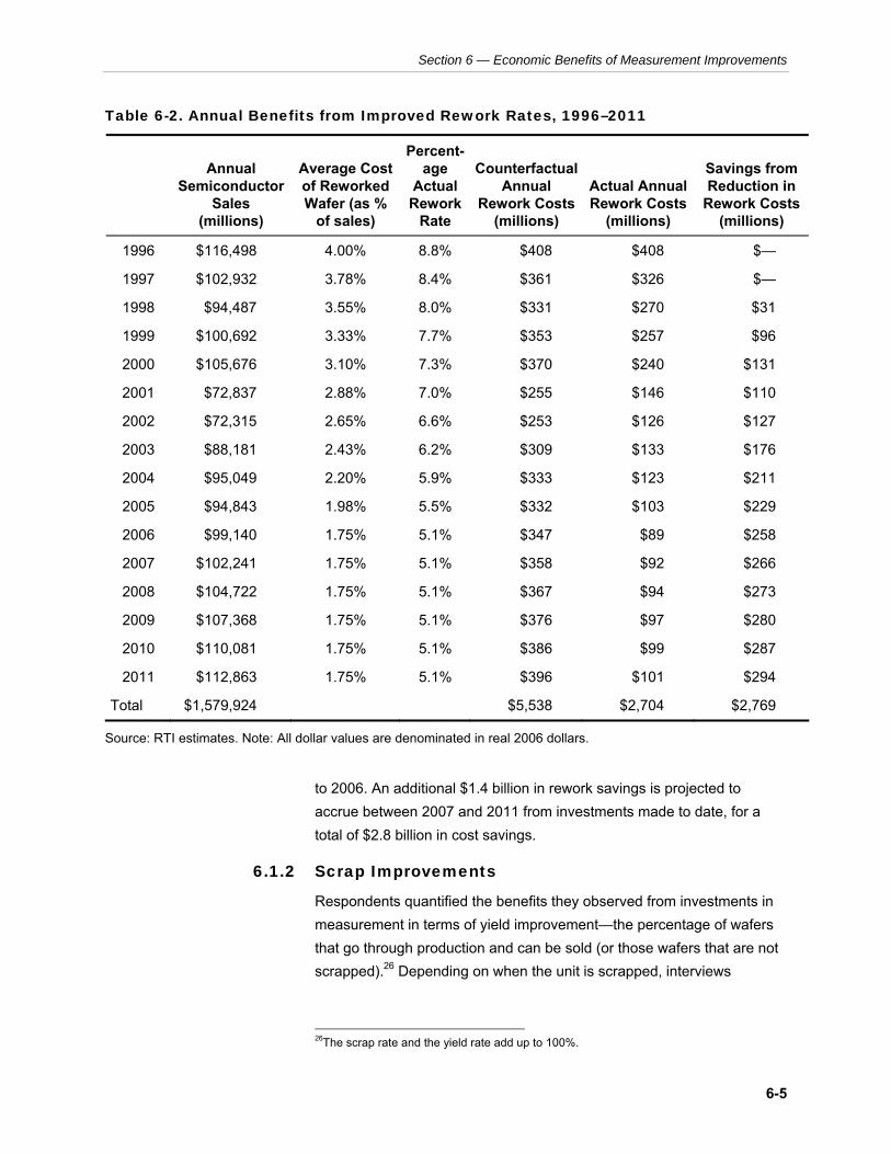
Section 6 — Economic Benefits of Measurement Improvements
Table 6-2. Annual Benefits from Improved Rework Rates, 1996–2011
Percent- Annual Average Cost age Counterfactual Savings from
Semiconductor of Reworked Actual Annual Actual Annual Reduction in Sales Wafer (as % Rework Rework Costs Rework Costs Rework Costs
(millions) of sales) Rate (millions) (millions) (millions)
1996 $116,498 4.00% 8.8% $408 $408 $—
1997 $102,932 3.78% 8.4% $361 $326 $—
1998 $94,487 3.55% 8.0% $331 $270 $31
1999 $100,692 3.33% 7.7% $353 $257 $96
2000 $105,676 3.10% 7.3% $370 $240 $131
2001 $72,837 2.88% 7.0% $255 $146 $110
2002 $72,315 2.65% 6.6% $253 $126 $127
2003 $88,181 2.43% 6.2% $309 $133 $176
2004 $95,049 2.20% 5.9% $333 $123 $211
2005 $94,843 1.98% 5.5% $332 $103 $229
2006 $99,140 1.75% 5.1% $347 $89 $258
2007 $102,241 1.75% 5.1% $358 $92 $266
2008 $104,722 1.75% 5.1% $367 $94 $273
2009 $107,368 1.75% 5.1% $376 $97 $280
2010 $110,081 1.75% 5.1% $386 $99 $287
2011 $112,863 1.75% 5.1% $396 $101 $294
Total $1,579,924 $5,538 $2,704 $2,769
Source: RTI estimates. Note: All dollar values are denominated in real 2006 dollars.
to 2006. An additional $1.4 billion in rework savings is projected to accrue between 2007 and 2011 from investments made to date, for a total of $2.8 billion in cost savings.
6.1.2 Scrap Improvements
Respondents quantified the benefits they observed from investments in measurement in terms of yield improvement—the percentage of wafers that go through production and can be sold (or those wafers that are not scrapped).26 Depending on when the unit is scrapped, interviews
26The scrap rate and the yield rate add up to 100%.
6-5
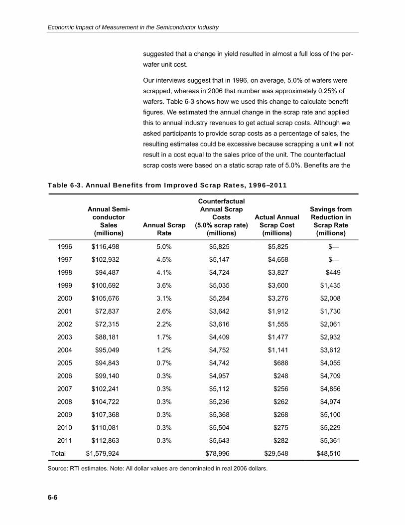
Economic Impact of Measurement in the Semiconductor Industry
suggested that a change in yield resulted in almost a full loss of the per-wafer unit cost.
Our interviews suggest that in 1996, on average, 5.0% of wafers were scrapped, whereas in 2006 that number was approximately 0.25% of wafers. Table 6-3 shows how we used this change to calculate benefit figures. We estimated the annual change in the scrap rate and applied this to annual industry revenues to get actual scrap costs. Although we asked participants to provide scrap costs as a percentage of sales, the resulting estimates could be excessive because scrapping a unit will not result in a cost equal to the sales price of the unit. The counterfactual scrap costs were based on a static scrap rate of 5.0%. Benefits are the
Table 6-3. Annual Benefits from Improved Scrap Rates, 1996–2011
Counterfactual Annual Semi- Annual Scrap Savings from
conductor Costs Actual Annual Reduction in Sales Annual Scrap (5.0% scrap rate) Scrap Cost Scrap Rate
(millions) Rate (millions) (millions) (millions)
1996 $116,498 5.0% $5,825 $5,825 $—
1997 $102,932 4.5% $5,147 $4,658 $—
1998 $94,487 4.1% $4,724 $3,827 $449
1999 $100,692 3.6% $5,035 $3,600 $1,435
2000 $105,676 3.1% $5,284 $3,276 $2,008
2001 $72,837 2.6% $3,642 $1,912 $1,730
2002 $72,315 2.2% $3,616 $1,555 $2,061
2003 $88,181 1.7% $4,409 $1,477 $2,932
2004 $95,049 1.2% $4,752 $1,141 $3,612
2005 $94,843 0.7% $4,742 $688 $4,055
2006 $99,140 0.3% $4,957 $248 $4,709
2007 $102,241 0.3% $5,112 $256 $4,856
2008 $104,722 0.3% $5,236 $262 $4,974
2009 $107,368 0.3% $5,368 $268 $5,100
2010 $110,081 0.3% $5,504 $275 $5,229
2011 $112,863 0.3% $5,643 $282 $5,361
Total $1,579,924 $78,996 $29,548 $48,510
Source: RTI estimates. Note: All dollar values are denominated in real 2006 dollars.
6-6
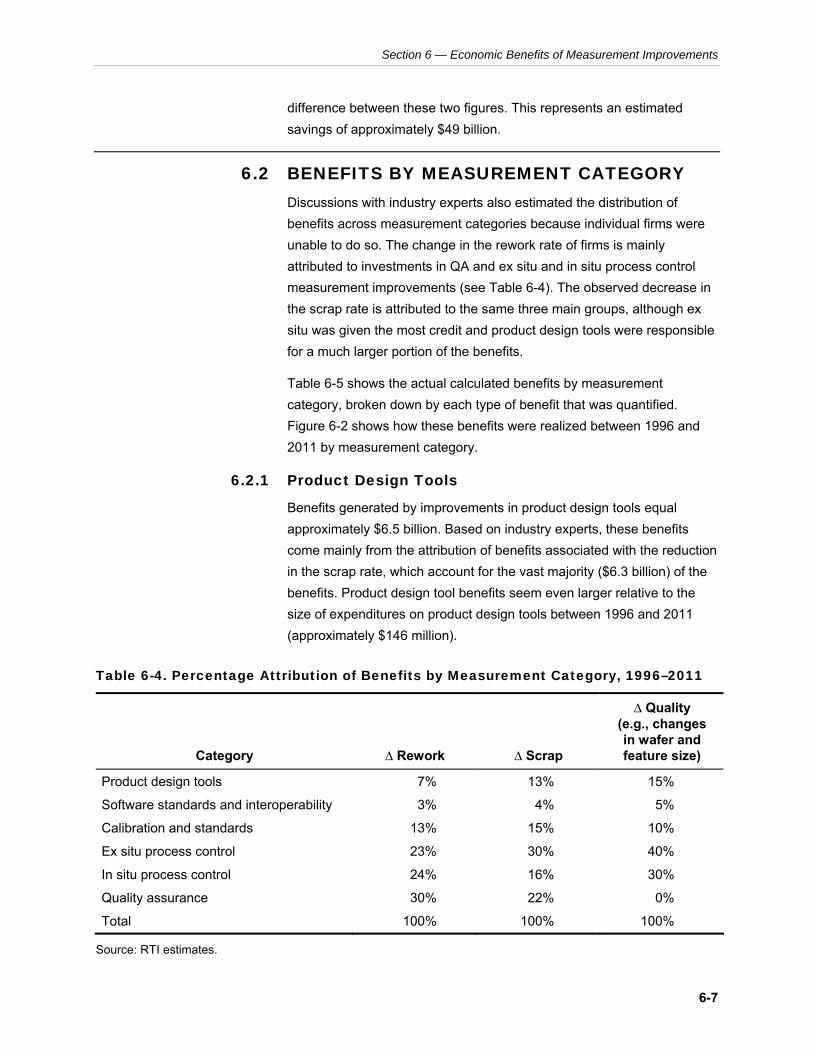
Section 6 — Economic Benefits of Measurement Improvements
difference between these two figures. This represents an estimated savings of approximately $49 billion.
6.2 BENEFITS BY MEASUREMENT CATEGORY Discussions with industry experts also estimated the distribution of benefits across measurement categories because individual firms were unable to do so. The change in the rework rate of firms is mainly attributed to investments in QA and ex situ and in situ process control measurement improvements (see Table 6-4). The observed decrease in the scrap rate is attributed to the same three main groups, although ex situ was given the most credit and product design tools were responsible for a much larger portion of the benefits.
Table 6-5 shows the actual calculated benefits by measurement category, broken down by each type of benefit that was quantified. Figure 6-2 shows how these benefits were realized between 1996 and 2011 by measurement category.
6.2.1 Product Design Tools
Benefits generated by improvements in product design tools equal approximately $6.5 billion. Based on industry experts, these benefits come mainly from the attribution of benefits associated with the reduction in the scrap rate, which account for the vast majority ($6.3 billion) of the benefits. Product design tool benefits seem even larger relative to the size of expenditures on product design tools between 1996 and 2011 (approximately $146 million).
Table 6-4. Percentage Attribution of Benefits by Measurement Category, 1996–2011
∆ Quality (e.g., changes in wafer and
Category ∆ Rework ∆ Scrap feature size)
Product design tools 7% 13% 15%
Software standards and interoperability 3% 4% 5%
Calibration and standards 13% 15% 10%
Ex situ process control 23% 30% 40%
In situ process control 24% 16% 30%
Quality assurance 30% 22% 0%
Total 100% 100% 100%
Source: RTI estimates.
6-7
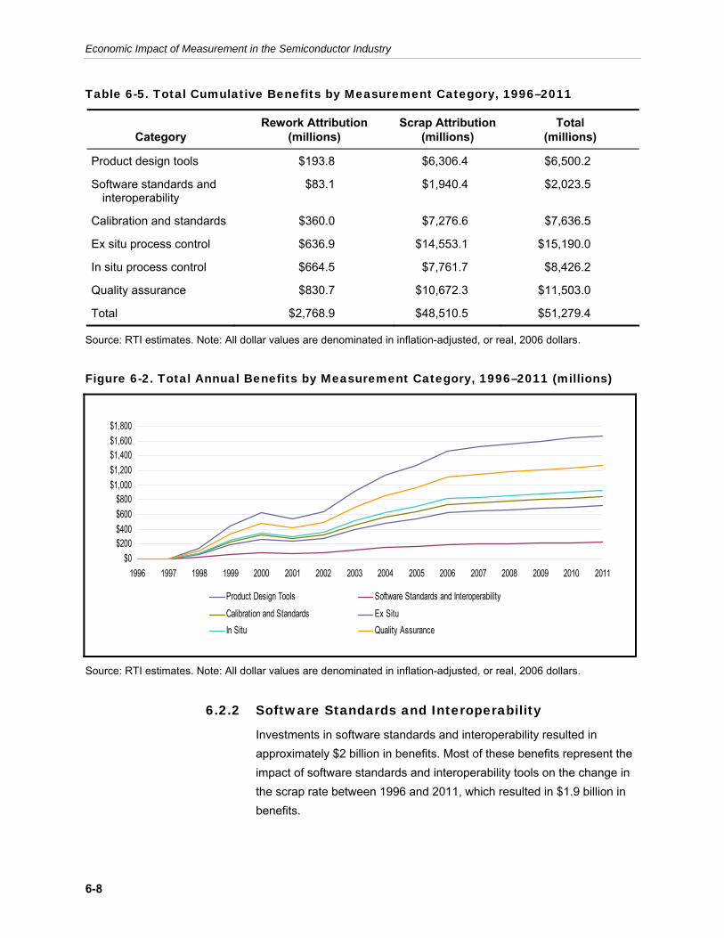
Economic Impact of Measurement in the Semiconductor Industry
Table 6-5. Total Cumulative Benefits by Measurement Category, 1996–2011
Rework Attribution Scrap Attribution Total Category (millions) (millions) (millions)
Product design tools $193.8 $6,306.4 $6,500.2
Software standards and $83.1 $1,940.4 $2,023.5 interoperability
Calibration and standards $360.0 $7,276.6 $7,636.5
Ex situ process control $636.9 $14,553.1 $15,190.0
In situ process control $664.5 $7,761.7 $8,426.2
Quality assurance $830.7 $10,672.3 $11,503.0
Total $2,768.9 $48,510.5 $51,279.4
Source: RTI estimates. Note: All dollar values are denominated in inflation-adjusted, or real, 2006 dollars.
Figure 6-2. Total Annual Benefits by Measurement Category, 1996–2011 (millions)
$1,800 $1,600 $1,400 $1,200 $1,000
$800 $600 $400 $200
$0 1996 1997 1998 1999 2000 2001 2002 2003 2004 2005 2006 2007 2008 2009 2010 2011
Product Design Tools Software Standards and Interoperability
Calibration and Standards Ex Situ In Situ Quality Assurance
Source: RTI estimates. Note: All dollar values are denominated in inflation-adjusted, or real, 2006 dollars.
6.2.2 Software Standards and Interoperability
Investments in software standards and interoperability resulted in approximately $2 billion in benefits. Most of these benefits represent the impact of software standards and interoperability tools on the change in the scrap rate between 1996 and 2011, which resulted in $1.9 billion in benefits.
6-8
Section 6 — Economic Benefits of Measurement Improvements
6.2.3 Calibration and Standard Test Methods
New calibration and standard test methods helped generate almost $7.6 billion in benefits. These investments mainly affected the scrap rate ($7.3 billion in benefits attributed).
6.2.4 Ex Situ Process Control
Benefits stemming from improved ex situ process control measurement technologies were the second highest of any category, with $37 billion, trumped only by QA investment-related benefits. Ex situ technologies had the largest impact of any measurement category on the reduction in the scrap rate ($14.5 billion attributed).
6.2.5 In Situ Process Control
Investments in in situ process control measurement technologies resulted in $8.4 billion in benefits; $7.8 billion in scrap reduction benefits are attributed to in situ investments. Although in situ process control was largely nonexistent in 1996, investments between 1996 and 2011 had a significant impact on the industry.
6.2.6 Quality Assurance
New QA techniques and technologies helped generate the largest benefits of any measurement category. Investments made in QA resulted in approximately $11.5 billion in benefits between 1996 and 2011. Of any measurement category, the most rework benefits ($830.7 million) are attributed to QA, and the second most are attributed to scrap reduction benefits of $10.7 billion.
6.3 MEASURES OF ECONOMIC RETURN This section provides an overview of the relationship between the semiconductor industry’s expenditures on measurement standards and technologies between 1996 and 2006 and key benefits accrued to industry stakeholders from 1997 to 2011. We show the time series of costs and benefits and then provide summary impact metrics from our study, including NPV figures, net benefit estimates, and cost-benefit ratios for the industry as a whole and, in some cases, broken out by stakeholder group and measurement category.
6.3.1 Time Series of Costs and Benefits
Table 6-6 provides an overview of the annual costs and benefits incurred by the semiconductor industry, and Figures 6-3 and 6-4 show these
6-9
Economic Impact of Measurement in the Semiconductor Industry
6.3.2
costs graphically for purposes of comparison annually and cumulatively. Costs are calculated from 1996 to 2006 and include both investment costs in new technologies and standards and ongoing variable costs. Total fixed investment costs during the period of focus are estimated to have been approximately $5.2 billion, while variable costs are estimated at $2.3 billion. Total stakeholder costs are estimated to have been $7.5 billion, plus over $3 billion spent by NIST and other consortia. Benefits are also shown broken down by category—$48.5 billion for scrap rate reduction and $2.8 billion for rework rate reduction for a total of $51.3 billion.
Performance Measures
Net benefits from stakeholder, government, and other investments equaled $38.9 billion. The NPV of these investments is $17.2 billion. Annual benefits surpassed annual costs in 2001, although cumulative benefits did not surpass cumulative costs until 2006, as shown in Figures 6-3 and 6-4. Table 6-7 provides summary information on net benefits at the measurement category level. As an industry and for all measurement categories, the investments result in very significant net benefits.
All investments by measurement category show positive returns on investment, with in situ showing the largest net benefit ($15 billion) and software standards showing the least ($2 billion). However, investments in product design tools seem to result in the largest benefit-cost ratio; an investment of $1 in product design tools resulted in more than $45.5 in benefits.
Table 6-8 presents several overall performance metrics. The NPV of benefits made between 1996 and 2006, based on benefits accrued between 1997 and 2011, is $17 billion. The BCR is 3.3, meaning that for every $1 invested in measurement, the industry saw a $3.30 benefit. The IRR of 67% similarly suggests a significantly positive rate of return on these investments.
Again, of note, we did not quantify the quality improvement benefits associated with investments in new measurement technology and standards. Quality benefits include a significant reduction in feature size and hence major improvements in downstream benefits to businesses and consumers who use products with semiconductors as supporting technology. We did estimate the share of quality benefits that are
6-10
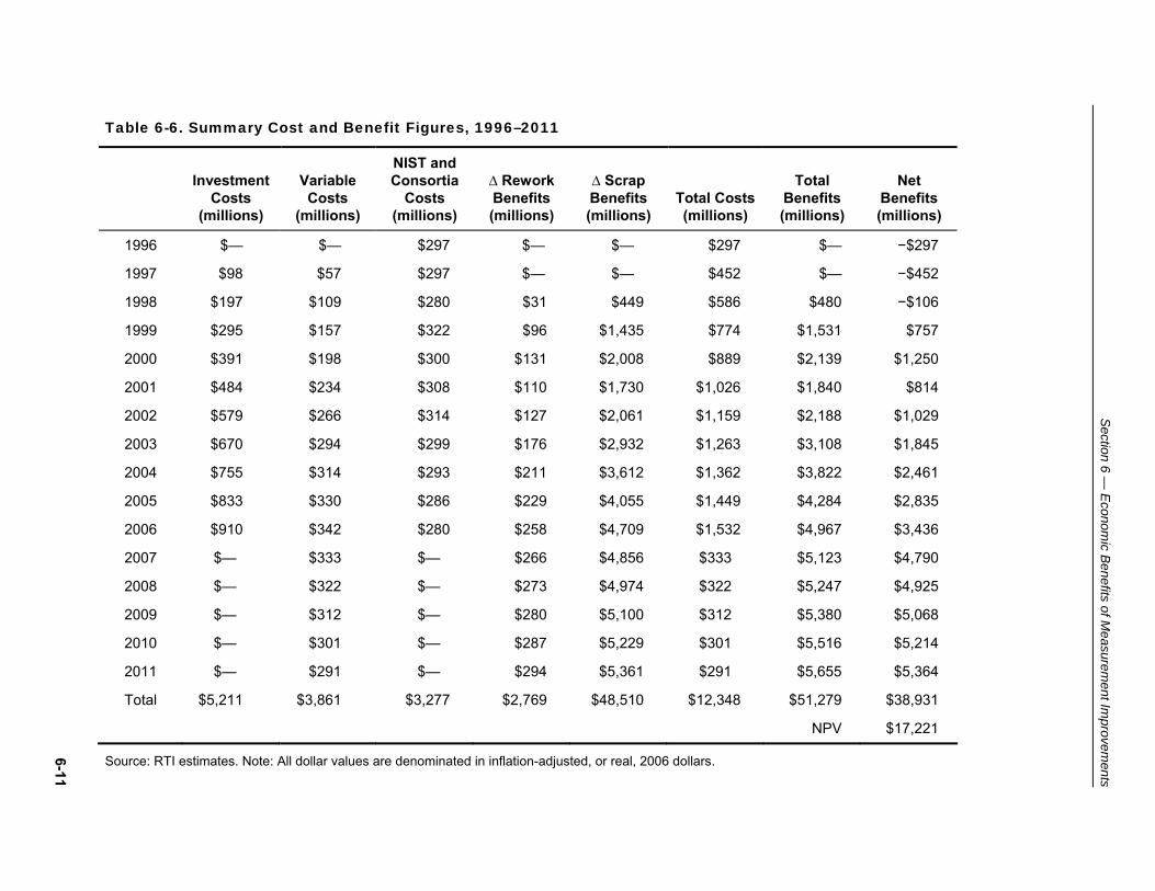
Table 6-6. Summary Cost and Benefit Figures, 1996–2011
NIST and Investment Variable Consortia ∆ Rework ∆ Scrap Total Net
Costs Costs Costs Benefits Benefits Total Costs Benefits Benefits (millions) (millions) (millions) (millions) (millions) (millions) (millions) (millions)
1996 $— $— $297 $— $— $297 $— −$297
1997 $98 $57 $297 $— $— $452 $— −$452
1998 $197 $109 $280 $31 $449 $586 $480 −$106
1999 $295 $157 $322 $96 $1,435 $774 $1,531 $757
2000 $391 $198 $300 $131 $2,008 $889 $2,139 $1,250
2001 $484 $234 $308 $110 $1,730 $1,026 $1,840 $814
2002 $579 $266 $314 $127 $2,061 $1,159 $2,188 $1,029
2003 $670 $294 $299 $176 $2,932 $1,263 $3,108 $1,845
2004 $755 $314 $293 $211 $3,612 $1,362 $3,822 $2,461
2005 $833 $330 $286 $229 $4,055 $1,449 $4,284 $2,835
2006 $910 $342 $280 $258 $4,709 $1,532 $4,967 $3,436
2007 $— $333 $— $266 $4,856 $333 $5,123 $4,790
2008 $— $322 $— $273 $4,974 $322 $5,247 $4,925
2009 $— $312 $— $280 $5,100 $312 $5,380 $5,068
2010 $— $301 $— $287 $5,229 $301 $5,516 $5,214
2011 $— $291 $— $294 $5,361 $291 $5,655 $5,364
Total $5,211 $3,861 $3,277 $2,769 $48,510 $12,348 $51,279 $38,931
NPV $17,221
Section 6 —
Econom
ic Benefits of M
easurement Im
provements
Source: RTI estimates. Note: All dollar values are denominated in inflation-adjusted, or real, 2006 dollars. 6-11
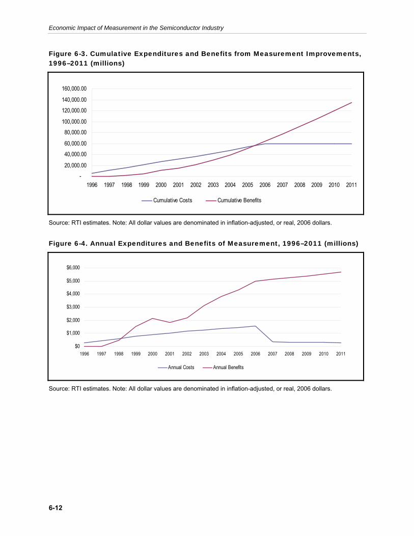
Economic Impact of Measurement in the Semiconductor Industry
Figure 6-3. Cumulative Expenditures and Benefits from Measurement Improvements, 1996–2011 (millions)
160,000.00
140,000.00
120,000.00
100,000.00
80,000.00
60,000.00
40,000.00
20,000.00
-1996 1997 1998 1999 2000 2001 2002 2003 2004 2005 2006 2007 2008 2009 2010 2011
Cumulative Costs Cumulative Benefits
Source: RTI estimates. Note: All dollar values are denominated in inflation-adjusted, or real, 2006 dollars.
Figure 6-4. Annual Expenditures and Benefits of Measurement, 1996–2011 (millions)
$6,000
$5,000
$4,000
$3,000
$2,000
$1,000
$0 1996 1997 1998 1999 2000 2001 2002 2003 2004 2005 2006 2007 2008 2009 2010 2011
Annual Costs Annual Benefits
Source: RTI estimates. Note: All dollar values are denominated in inflation-adjusted, or real, 2006 dollars.
6-12
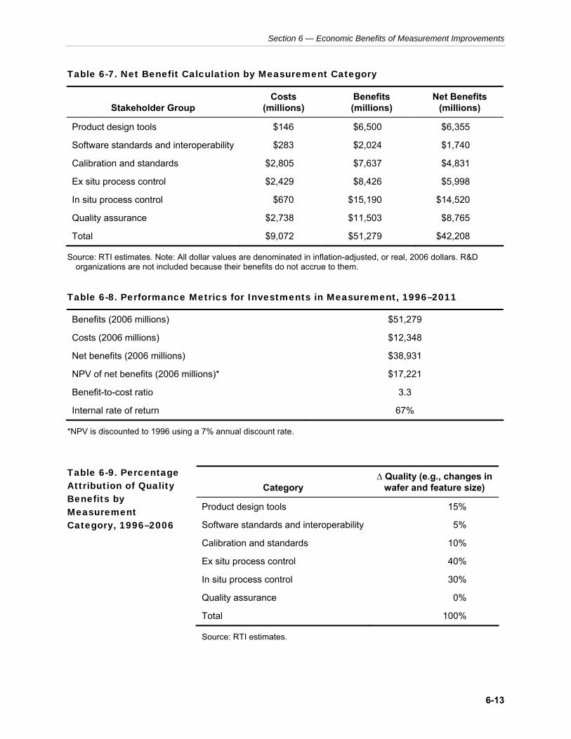
Section 6 — Economic Benefits of Measurement Improvements
Table 6-7. Net Benefit Calculation by Measurement Category
Costs Benefits Net Benefits Stakeholder Group (millions) (millions) (millions)
Product design tools $146 $6,500 $6,355
Software standards and interoperability $283 $2,024 $1,740
Calibration and standards $2,805 $7,637 $4,831
Ex situ process control $2,429 $8,426 $5,998
In situ process control $670 $15,190 $14,520
Quality assurance $2,738 $11,503 $8,765
Total $9,072 $51,279 $42,208
Source: RTI estimates. Note: All dollar values are denominated in inflation-adjusted, or real, 2006 dollars. R&D organizations are not included because their benefits do not accrue to them.
Table 6-8. Performance Metrics for Investments in Measurement, 1996–2011
Benefits (2006 millions) $51,279
Costs (2006 millions) $12,348
Net benefits (2006 millions) $38,931
NPV of net benefits (2006 millions)* $17,221
Benefit-to-cost ratio 3.3
Internal rate of return 67%
*NPV is discounted to 1996 using a 7% annual discount rate.
Table 6-9. Percentage Attribution of Quality Benefits by Measurement Category, 1996–2006
∆ Quality (e.g., changes in Category wafer and feature size)
Product design tools 15%
Software standards and interoperability 5%
Calibration and standards 10%
Ex situ process control 40%
In situ process control 30%
Quality assurance 0%
Total 100%
Source: RTI estimates.
6-13

Economic Impact of Measurement in the Semiconductor Industry
attributable to investments in each measurement category. Table 6-9 provides an overview of such benefits based on expert and stakeholder opinions.
6.4 UNCERTAINTIES AND DATA LIMITATIONS Analyzing economic costs and benefits from as broad a suite of technologies and improvements as this study’s is accompanied by data uncertainty and limitations. Although every effort was made to minimize uncertainty, it is impossible to eliminate it. Principal sources of uncertainty in this analysis stem from the following:
• Accurately describing, accounting for, and assigning costs and benefits to measurement improvements. Respondents were presented with a detailed taxonomy of measurement infrastructure and improvements. They were asked to limit their responses to the study time frame and suite of measurement technologies; however, it is possible that they included costs and benefits from technologies that were out of scope.
• Interviewer bias. Many data were captured during in-person and telephone interviews and thus are subject to biases stemming from how questions were asked and how responses were recorded.
• Time. The quantitative analysis spans a decade, and time introduces two sources of uncertainty. First, respondents’ memories of technology development costs and benefits from improvements may not be as accurate for 1996 as for 2006. Second, the time series of estimated benefits and expenditures are based on average technology adoption data from the survey; respondents may not have recalled their actual adoption pattern with great accuracy.
• Valuing costs and benefits as a percentage of sales. The breadth of technologies, methods, and systems investigated required the use of a readily available measure for capturing costs and benefits. The uncertainty stemming from the U.S. Census estimates of the value of shipments, the analysis’s proxy for sales revenue, was carried forward into this analysis. In addition, respondents needed to estimate the percentage of their firms’ annual sales for which their cost and benefit estimates were valid.
• Counterfactual analysis. The counterfactual analysis held key productivity values from 1996 constant and quantified as benefits the annual improvement in those metrics. The state-of-the-art was assumed to have not changed over those 10 years, which is unlikely. However, it was not possible to derive an alternative counterfactual in which measurement would have improved to some degree, but not to the same extent as actually occurred. Presenting such a counterfactual would have made valuing costs
6-14
Section 6 — Economic Benefits of Measurement Improvements
and benefits challenging because of the nuance in presenting stakeholders with even more intricate scenarios.
Finally, the industry would have grown differently in the absence of measurement improvements. If it is true that improved measurement capabilities enabled dramatic gains in semiconductor quality, processing speed, and feature density, and that all of these gains enabled innovation in electronics and computing, then it follows that, without them, many of these gains would not have been possible. Annual semiconductor sales revenue would have been different as would the investment decisions from firms in the semiconductor supply chain. Thus, assuming the status quo in measurement from end-of-year 1995 and combining that assumption with actual annual sales from 1996 to 2006 present challenges in interpreting results.
The costs and benefits analyzed in this report are relative to the state-of-the-art in measurement existing in 1995. Economic benefits in particular are therefore denominated in that technology currency and must be cautiously interpreted as such.
6-15

7 Conclusion
The semiconductor industry and the R&D organizations like NIST and SEMATECH that support it developed and implemented dramatic improvements in the measurement infrastructure between 1996 and 2006. These advances increased the U.S. semiconductor industry’s global competitiveness while simultaneously invigorating the industries that depend on semiconductors by providing greater processing power more quickly and at a lower cost. Yet the ultimate beneficiaries are the businesses and consumers whose productivity, enjoyment, and quality of life have increased from the many electronic and computing products semiconductors enable. NIST’s investments and those of consortia have helped keep U.S. companies at the forefront of the most advanced semiconductor technology.
The many interviewees, academics, and other experts who participated in this study offered their views not only on how measurement improvements affected the industry, but also on the next set of technical barriers the industry faces as it continues to innovate.
7.1 ECONOMIC RETURNS FROM COORDINATED MEASUREMENT R&D STRATEGY As this study found, firms throughout the semiconductor supply chain realized the need for significant investments in measurement standards and technology. However, the R&D, technical support, and coordination provided by NIST and pooled through organizations like SEMATECH over the past several decades have been essential to the success of the industry.
NIST’s ability to address industry standards and measurement needs has ensured the progress and prosperity of the U.S. semiconductor
7-1
Economic Impact of Measurement in the Semiconductor Industry
industry (ASTRA, 2007). A recent NIST assessment of the U.S. measurement system showed that NIST’s support of technological innovation through its standards-related activities played and continues to play a critical role in maintaining a U.S. competitive advantage in the world economy, including the semiconductor industry (NIST, 2007).
SEMATECH is also credited with enabling the U.S. semiconductor industry to develop cooperative standards (Browning, 1995), and its leadership on industry roadmaps provides evidence of how coordinated research strategies for generic technologies and standardization can effectively overcome technical and market barriers in advanced technology fields. Testifying before the Board on Science, Technology, and Economic Policy of the National Academy of Sciences, Mr. Clark McFadden, a lawyer with extensive experience within the technology policy community, stated that SEMATECH’s “fostering of an industry perspective on technology development, leading naturally to industry-wide testing of tools and standards and to the development of industry-wide technology roadmaps” (NAS, 2003, p. 95).
As in any industry, semiconductor firms compete aggressively with each other; however, motivated and supported by NIST and other consortia, these companies have put significant time and effort into developing and supporting generic technologies and standards that have helped the entire industry. Our interviews and data collection efforts suggest that industry stakeholders spent approximately $10 billion between 1996 and 2006 adopting new measurement standards and technologies. NIST, SEMATECH, SEMI, and SRC also spent approximately $3 billion on standards and coordination-related efforts during this period. In combination, these investments had a profound effect on the industry.
We quantified economic benefits for improvements relative to state-of-the-art measurement technologies in place in 1996. The rate of scrap— the percentage of wafers that are thrown out—decreased from 7.53% to 0.28%. This resulted in approximately $49 billion in savings. The cost of rework decreased from 4.0 % to 1.75%, and the rate of rework decreased from 8.8% to 5.1%. This resulted in approximately $2.8 billion in savings for the industry. Economic benefits, while measured in billions, represent a small, though significant, fraction of total industry revenues.
Table 7-1 presents overall quantitative performance metrics. Combining the private-sector investments with quantified cost-saving benefits that
7-2
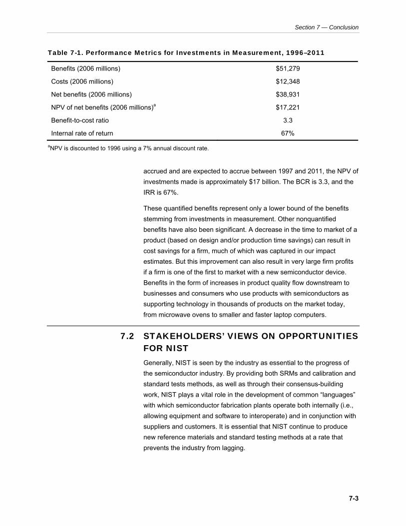
Section 7 — Conclusion
Table 7-1. Performance Metrics for Investments in Measurement, 1996–2011
Benefits (2006 millions) $51,279
Costs (2006 millions) $12,348
Net benefits (2006 millions) $38,931
NPV of net benefits (2006 millions)a $17,221
Benefit-to-cost ratio 3.3
Internal rate of return 67%
aNPV is discounted to 1996 using a 7% annual discount rate.
accrued and are expected to accrue between 1997 and 2011, the NPV of investments made is approximately $17 billion. The BCR is 3.3, and the IRR is 67%.
These quantified benefits represent only a lower bound of the benefits stemming from investments in measurement. Other nonquantified benefits have also been significant. A decrease in the time to market of a product (based on design and/or production time savings) can result in cost savings for a firm, much of which was captured in our impact estimates. But this improvement can also result in very large firm profits if a firm is one of the first to market with a new semiconductor device. Benefits in the form of increases in product quality flow downstream to businesses and consumers who use products with semiconductors as supporting technology in thousands of products on the market today, from microwave ovens to smaller and faster laptop computers.
7.2 STAKEHOLDERS’ VIEWS ON OPPORTUNITIES FOR NIST Generally, NIST is seen by the industry as essential to the progress of the semiconductor industry. By providing both SRMs and calibration and standard tests methods, as well as through their consensus-building work, NIST plays a vital role in the development of common “languages” with which semiconductor fabrication plants operate both internally (i.e., allowing equipment and software to interoperate) and in conjunction with suppliers and customers. It is essential that NIST continue to produce new reference materials and standard testing methods at a rate that prevents the industry from lagging.
7-3
Economic Impact of Measurement in the Semiconductor Industry
Moving forward, firms in the industry will continue their private R&D efforts to shrink feature size, increase wafer size, and evaluate and research new materials. In the coming years, the industry will continue to work on these three main areas, but experts and stakeholders see many areas where problems of measurement exist and where technologies and standards will be needed to prevent technical roadblocks.
Based on the 2005 ITRS Roadmap, in general the challenges presented in the coming years relate to three main areas:
• reduction in feature sizes
• new interconnect technology, including three-dimensional interconnects
• tighter control of electrical parameters
One near-term challenge is to develop linewidths greater than or equal to 32 nm by 2013. Accomplishing this objective will require increased integration of, and data management for, inline and in situ process controls and sensors. The industry anticipates migrating toward new starting materials, such as silicon on insulator (SOI) and, therefore, will require better approaches for particle detection. New techniques for measuring trench depth and sidewall roughness will also be needed in connection with the use of low-κ dielectrics (ITRS, 2005).
At line widths below 32 nm, the challenges become even more complex and will require innovative thinking and measurement-related investments well in advance of using 32-nm equipment in a production environment. In many cases, the materials and processes that will be used past 2013 are unknown, leaving the measurement needs undefined. It is possible that the desired scaling will one day require measurements to be made at the atomic level.
In particular, stakeholders and experts mentioned measurement and standards needs in several key technical areas:
• New standards for measuring feature lengths at 32 nm: Several equipment manufacturers mentioned that new standards are needed for the looming shift from feature lengths of 65 nm to 32 nm. Although many manufacturers are still operating at the 90-nm level and above, the most advanced processing plants are currently at 65 nm, and, according to several equipment manufacturers and front-end processing firms, there are no standards available at these new levels. Further, wafer calibration standards and gas and liquid standards are needed to reach smaller sizes.
7-4
Section 7 — Conclusion
• New techniques for measuring radio-frequency electromagnetic energy and high-frequency magnetic fields: Another equipment manufacturer said that measuring energy and chemical flow is very difficult currently because of the complexity involved in controlling radio frequency power and high-frequency magnetic fields. As the semiconductor industry strives to fabricate smaller structures, the requirement for more precise control of the flow of materials and power continues to increase.
• New techniques for conducting pressure-based measurements: Chemical and materials suppliers indicated that they are trying to move toward pressure-based measurements that could significantly increase accuracy of liquid and gas measurements. Accurate control of mass flow is essential for providing precise amounts of materials for individual processing steps. Knowledge of the pressure is an essential component of controlling the amount of material that is delivered to processing equipment.
• Improved mask measurement standards: Front-end processing firms mentioned that more measurement standards are needed for mask measurement and depth measurement. Mask measurement equipment is needed to make sure that features are exactly to the specifications of the designers.
• Improved chemical and materials standards and processes: Process engineering needs are generally met more quickly than chemical and materials needs. Although significant work on low-k dielectric materials has already been conducted, particularly by NIST, more work is needed before the industry can seamlessly adopt these materials.
• New calibration and standard test methods: Although the adoption of calibration and standard test methods would appear to be an insignificant activity, many respondents indicated that the development of new calibration and standard test methods, including reference materials, is often delayed as compared to industry needs. When a new technology is first introduced, the standard test methods are often still under development and limit full commercialization of the breakthrough. This lag is one of the reasons for low initial yields typically observed during deployment of new technologies.
For example, a large body of standards is available for silicon semiconductors including resistivity, depth profiling, and other physical attributes. Smaller feature sizes have driven the need for improved z-axis resolution in silicon calibration standards that are used to measure depth profiles and dopant implantation. Depth profile standards have migrated from a series of stack thin layers of roughly 100-nm thickness to hundreds of stacked layers of approximately 10-nm thickness. The new generation of depth profile standards leverages quantum-confined superlattices to ensure accurate z-dimension control. However, corresponding SRMs are often not available for the new compound semiconductor substrates (e.g., SiGe).
• Better inoperability standards: Many stakeholders suggested that there is a need for more interoperability standards and
7-5
Economic Impact of Measurement in the Semiconductor Industry
technologies, as the industry moves forward, to ensure an efficient transition of structures from designer to mask maker to verification in the fabrication facility.
Throughout all discussions of future industry measurement needs, a common theme was the relative importance of consistency in measurement as opposed to accuracy. While accuracy is important, being able to consistently replicate measurements allows for adjustments to production processes that are based on known measurement results. A focus on technologies and standards that are consistent is critical to the industry’s success.
Past investments in semiconductor measurement standards and technologies have proven to be very beneficial both to the industry and to businesses and consumers. It is essential that investment in and collaboration on standards and technology development and on common goal-setting efforts continue. And to that end, the industry requires that NIST play a significant role.
7-6

References
Aizcorbe, A. March 2002. Why Are Semiconductor Prices Falling So Fast? Industry Estimates and Implications for Productivity Measurement. Federal Reserve Board. Available at <http://ideas.repec.org/p/fip/fedgfe/2002-20.html>.
Alliance for Science and Technology Research in America (ASTRA). 2007. Written Testimony of Dr. Stanley Williams, Hewlett-Packard Quantum Research Group on behalf of ASTRA, The Alliance for Science and Technology Research in America, Before the House Science and Technology Committee. Subcommittee on Technology and Innovation. Washington, DC: ASTRA.
Bharadwaj, S., S.G. Bharadwaj, and B. Konsynski. 1999. “Information Technology on Firm Performance as Measured by Tobin’s q.” Management Science 45(6):1008-1024.
Bresnahan, T., E. Brynjolfsson, and L. Hitt. 2002. “Information Technology, Workplace Organization, and the Demand for Skilled Labor: Firm-Level Evidence.” Quarterly Journal of Economics 117(1):339-376.
Browning, L., J. Beyer, and J. Shetler. February 1995. The Academy of Management Journal 38(1):113-151.
Brynjolfsson, E., and L. Hitt. 1996. “Paradox Lost? Firm-Level Evidence on the Returns to Information Systems Spending.” Management Science 42(4):541-558.
Dewan, S., and C. Min. 1997. “The Substitution of Information Technology for Other Factors of Production: A Firm Level Analysis.” Management Science 43(12):1660-1675.
“Executive Roundup: What 2006 Has in Store.” 2006. Semiconductor International. 29(1):52-59.
Fandel, D. 2006. “Industry Capacity and Productivity Trends.” International Sematech Manufacturing Initiative. Presentation. January 26, 2006.
R-1
Economic Impact of Measurement in the Semiconductor Industry
Gerold, D., R. Hershey, K. Mc Brayer, and J. Sturtevant. September 1997. Run-to-Run Control Benefits of Photolithography. Sematech AEC/APC Workshop IX. Incline Village, NV.
Gordon, R. February 14, 2006. “Forecast: Semiconductors, Worldwide, 2002-2010.” (1Q06 Update). Gartner.
Grimm, B. February 1998. “Price Indexes for Selected Semiconductors, 1974-1976.” Survey of Current Business. Available at <http://www.bea.gov/bea/articles/NATIONAL/NIPA/ 1998/0298od.pdf>.
International Technology Roadmap for Semiconductors (ITRS). 2005. Metrology Roadmap, page 35.
Jorgenson, D.W., and C.W. Wessner, eds. 2004. Productivity and Cyclicality in Semiconductors: Trends, Implications, and Questions—Report of a Symposium. Committee on Measuring and Sustaining the New Economy, National Research Council. Washington, DC: National Academies Press.
Jula, P. 2001. “The Economic Impact of Metrology Methods in Semiconductor Manufacturing.” Department of Electrical Engineering and Computer Science, University of California, Berkley, M.S. Project Report.
Lammers, D. 1998. “IBM’s Copper Interconnects Hit the Market.” EETimes. September 3.
Lichtenberg, F.R. 1995. “The Output Contributions of Computer Equipment and Personnel: A Firm-Level Analysis.” Economics of Innovation and New Technology 3(4):201-214.
Mautz, K.E. 2000. “Capability for 300mm: Approaching Industry Goals.” Semiconductor International. July 1.
National Academy of Sciences (NAS). 2003. “Board on Science, Technology, and Economic Policy: Securing the Future: Regional and National Programs to Support the Semiconductor Industry.” Washington, DC: NAS.
Rieppo, P. October 14, 2005. “Market Profile: Semiconductor Industry.” Gartner.
Semiconductor Industry Association (SIA). 2006. “Global Billings Report History (3-month moving actuals): 1976 – September 2007.” http://www.sia-online.org/downloads/GSR1976-present.xls.
Semiconductor Industry Association (SIA). 2005. “2020 is Closer than You Think.” Annual Report. Available at <http://www.sia-online.org/downloads/SIA_AR_2005.pdf>.
R-2
References
Spencer, B., L. Wilson, and R. Doering, The Semiconductor Technology Roadmap, FutureFab International, Vol. 18, January 12, 2005. Available at http://www.future-fab.com/documents.asp?d_ID=3004.
Tassey, G. 2005. Underinvestment in Public Good Technologies. Journal of Technology Transfer 30,(1/2):89-113.
Tassey, G. 2003. Methods for Assessing the Economic Impact of Government R&D. NIST Planning Report 03-1.
Triplett, J. 1996. High-Tech Industry Productivity and Hedonic Price Indices. Available at <http://www1.oecd.org/dsti/sti/stat-ana/prod/measurement.htm>. Last updated in August 2000.
U.S. General Accountability Office (GAO). July 1992. SEMATECH’s Technological Progress and Proposed R&D Program. Washington, DC: GAO.
U.S. National Institute of Standards and Technology (NIST). 2000. NIST Manufacturing Research and Services. Gaithersburg, MD: NIST.
U.S. National Institute of Standards and Technology (NIST). 2007. An Assessment of the United States Measurement System: Addressing Measurement Barriers to Accelerate Innovation. Gaithersburg, MD: NIST.
R-3

Appendix A: Expanded Technical Discussion
This appendix is an expanded version of Chapter 3; it offers a more in-depth technical discussion of the measurement improvements adopted by the semiconductor industry that are analyzed in the main body of the report. The discussion that follows is written for members of the scientific and engineering community.
This study defined measurement broadly to include metrology systems and standards. It grouped measurement advances between 1996 and 2006 into several major categories that map closely with the NTRS and ITRS:
• product design tools
• software standards and interoperability
• calibration and standard test methods
• ex situ process control techniques
• in situ process control techniques
• quality assurance
Figure A-1 provides several examples for each of the six categories listed above, as well as an overview of how the categories relate to semiconductor production. The figure does not include supporting organizations such as industry consortia and other R&D groups. However, we do recognize that these entities play an important role in developing the measurement infrastructure, and their activities were included in the economic analysis and qualitative review.
A-1
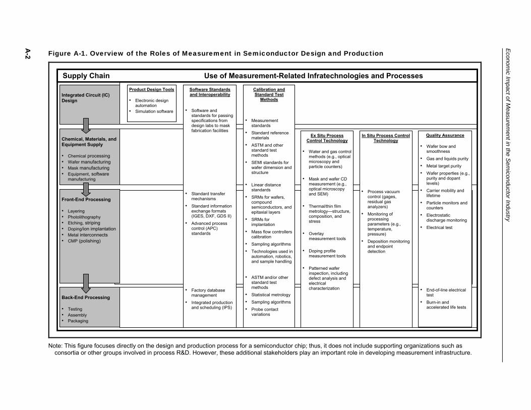
Figure A-1. Overview of the Roles of Measurement in Semiconductor Design and Production
Supply Chain Use of Measurement-Related Infratechnologies and Processes
Integrated Circuit (IC) Design
Product Design Tools
• Electronic design automation
• Simulation software
Software Standards and Interoperability
• Software and standards for passing specifications from
Calibration and Standard Test
Methods
• Measurement
Chemical, Materials, and
fabrication facilities design labs to mask
• Standard reference materials
standards
Ex Situ Process Control Technology
In Situ Process Control Technology
Quality Assurance
Equipment Supply • ASTM and other standard test • Water and gas control
• Wafer bow and smoothness
• Chemical processing • Wafer manufacturing • Mask manufacturing • Equipment, software
manufacturing • Linear distance
methods
• SEMI standards for wafer dimension and structure
•
methods (e.g., optical microscopy and particle counters)
Mask and wafer CD measurement (e.g., optical microscopy
•
levels)
• Gas and liquids purity
• Metal target purity
Wafer properties (e.g., purity and dopant
Front-End Processing
• Layering • Photolithography • Etching, striping • Doping/ion implantation • Metal interconnects • CMP (polishing)
• Standard transfer mechanisms
• Standard information exchange formats (IGES, DXF, GDS II)
• Advanced process control (APC) standards
• SRMs for wafers, compound semiconductors, and epitaxial layers
• SRMs for implantation
• Mass flow controllers calibration
• Sampling algorithms
• Technologies used in automation, robotics, and sample handling
• ASTM and/or other standard test
standards and SEM)
• Thermal/thin film metrology—structure, composition, and stress
• Overlay measurement tools
• Doping profile measurement tools
• Patterned wafer inspection, including defect analysis and electrical
• Process vacuum control (gages, residual gas analyzers)
• Monitoring of processing parameters (e.g., temperature, pressure)
• Deposition monitoring and endpoint detection
lifetime
• Particle monitors and counters
• Electrostatic discharge monitoring
• Electrical test
• Carrier mobility and
Back-End Processing
• Testing • Assembly • Packaging
• Factory database management
• Integrated production and scheduling (IPS)
• Statistical metrology
• Sampling algorithms
• Probe contact variations
methods characterization • End-of-line electrical test
• Burn-in and accelerated life tests
Econom
ic Impact of M
easurement in the S
emiconductor Industry
Note: This figure focuses directly on the design and production process for a semiconductor chip; thus, it does not include supporting organizations such as consortia or other groups involved in process R&D. However, these additional stakeholders play an important role in developing measurement infrastructure.
A-2
Appendix A — Expanded Technical Discussion
A.1 PRODUCT DESIGN TOOLS Advanced measurement techniques are needed to lay the foundation for improved simulation models. With the increasing link between semiconductor design and manufacturing processes, product design tools are becoming ever more tightly coupled with the full range of measurement capabilities used in the semiconductor manufacturing process and will help define what should be measured.
Product design tools for the semiconductor industry are most often associated with electronic design automation (EDA) tools. EDA tools include a broad range of capabilities, including
• system-level design;
• logical, circuit and physical design;
• design verification;
• design test; and
• design for manufacturability (DFM).
Based on the most recent ITRS Roadmap, these EDA subcategories allow for the aggregation of specific tools into product- or system-level design activities while avoiding definitional changes across vendors or technology node migrations. However, the range of tools within these categories is often widely different in terms of functionality and users’ perceptions of costs and benefits.
The ITRS treats modeling and simulation, a major aspect of system-level design, as a cross-cutting infratechnology supporting all technology areas, not just design tools. Each of the product design tools that we considered includes both modeling and simulation tools as integral components.
The ITRS EDA categories were the foundation for the product design subcategories, and they were expanded to consider a broader range of software tools because some stand-alone tools on the market may not yet be included in major EDA frameworks or be regularly reported as part of the EDA marketplace. These included some simulation tools and product life-cycle management (PLM) systems.
A.1.1 Recent Developments
Over the past decade, the most critical product design tool contributions have come from the emergence of EDA tools. Key improvements included
A-3
Economic Impact of Measurement in the Semiconductor Industry
• developing functional verification systems and
• incorporating tools to support subwavelengh lithography.
Although derived from systems developed in the early 1980s, EDA came into its own in the late 1990s when device complexity forced the elimination of initial design fabrications. The development of functional verification systems within EDA design tools was critical to implementing 130-nm technologies. Also critical to achieving 130-nm technologies was the incorporation of DFM to support subwavelength lithography. Together, these two developments are among the greatest sources of productivity gains during the period of analysis.
Device and process simulation and PLM tools beyond those incorporated into EDA suites have begun to emerge and affect the industry, but the full impact of these systems remains to be realized.
Below we discuss four subcategories of semiconductor design tools:
• system design tools
• design for manufacturability (DFM)
• device and process simulation
• product life-cycle management (PLM)
System Design Tools
This subcategory of semiconductor design tools includes the initial specification, functional verification, and optimization of a semiconductor device resulting in a register transfer level (RTL) that specifies functionality, short of physical layout. Prior design systems lacked complete simulation capabilities and required time-consuming and costly design-build-test cycles that made it impossible to progress beyond the 180-nm technology milestone.
Functional verification ensures that a design performs as intended and is a key step within this subcategory. Functional verification includes logical simulation and hardware emulation using formal methods. Critical to this capability in both functionality and modeling were accelerated simulation capabilities that resulted from the availability of significantly improved platform power (32- to 64-bit capability). Enhancements included nascent parallel processing capabilities that allowed many system design functions to be performed in parallel rather than as a series of discrete steps run in batch mode. Hardware definition languages (HDLs) were also critical to enabling these systems.
A-4
Appendix A — Expanded Technical Discussion
Design for Manufacturability
DFM is the extension of lithography to subwavelength dimensions using optical proximity correction (OPC) and reticle-enhancement technology (RET) to account and correct for process distortions. These capabilities were critical to achieving the 130-nm technology node by extending optical photolithography without having to adapt to a radically new generation of machines that could no longer use traditional optical focusing techniques.
Although the application of OPC and RET techniques to photolithography provided the most substantial benefits over the relevant time period, DFM techniques are the basis for compensating for any known distortions in the manufacturing process, including etching, planarization, or deposition. As semiconductor dimensions shrink, DFM becomes increasingly important to compensate for both tool and physical variations at the chip level. DFM technologies are typically included as part of the suite of capabilities within leading EDA systems.
Device and Process Simulation
Device and process simulation technologies are stand-alone tools that have capabilities well beyond normal electronic circuit simulation, including the simulation of physics, optics, and thermal characteristics. Additionally, with an increasing mix of devices for a system on a chip (SoC), this category is expanding to include a broad range of additional capabilities to manage analog and radio frequency requirements. Also included are a variety of process simulations that, whether formally integrated or not, have an impact on the design process.
Product Life-Cycle Management
Although not currently incorporated into major EDA systems packages, PLM systems are beginning to play a role in tying together the diverse semiconductor supply chain. PLM capabilities complement the use of standards, interoperability, and information exchange between design and manufacturing.
A.1.2 Representative Suppliers
The major suppliers of semiconductor design tools—Cadence, Synopsis, and MentorGraphics—rose to prominence in the late 1990s. DFM capabilities are also integrated into each of these major EDA vendor's suites of solutions. Silvaco and Mathworks are among the major
A-5
Economic Impact of Measurement in the Semiconductor Industry
suppliers of device and process simulation tools that are not part of the major EDA vendors.
A.1.3 Future Trends
For system design, electronic system-level tools (ESL) are emerging that promise to replace RTL, particularly as the number of new chip starts reduces and as SoC complexity increases. Improving formal verification techniques will be particularly critical to enhance reliability, ease the current verification bottleneck, and help the growing design productivity gap.
As dimensions shrink, the ITRS also points to increasing challenges posed by power management and leakage.
Future DFM trends will very closely link design with measurement because increasing variability at both the physical and process levels will demand a shift to designing for fault tolerance rather than simply designing to pass testing requirements. This is likely to include a shift from rule-based systems to model-based systems and will increasingly link design with yield optimization. Additionally, adoption of new fault models, testing techniques, and allowances for appropriate critical dimensions may help avoid test equipment cost and speed limitations.
Finally, the adoption and adaptation of PLM may provide a framework to link increasingly diverse and geographically dispersed elements of the semiconductor value chain. In particular, general-purpose PLM systems that have been designed around traditional manufacturing value chains will need to be modified and specialized for the unique requirements of the semiconductor industry. This is likely to be done in conjunction with improved design tool interoperability based on data format and language standards, as discussed in the next category.
A.2 SOFTWARE STANDARDS AND INTEROPERABILITY Standards and interoperability have become an increasingly important theme for all software as end users fight against proprietary standards that tie them to individual vendors. However, in the case of software standards and interoperability, benefits go well beyond end users’ desires to avoid proprietary systems. The industry’s ability to define and implement interoperability standards has had a significant impact on its ability to meet key technology milestones. This became increasingly true
A-6
Appendix A — Expanded Technical Discussion
in the 1990s with the evolving diversity in the semiconductor industry and its increasing geographic dispersion.
However, developing new standards is often costly, given the need to identify and specify requirements of all stakeholders in the value chain and then to develop compromises among them. In addition, acceptance and implementation of standards typically involve many hidden costs (such as transition and translation of legacy systems and data) that have impacts beyond the vendor community. Therefore, the standards and interoperability issues are typically resolved as part of a broader community effort among stakeholder organizations.
A.2.1 Recent Developments
Two software standards and interoperability developments affecting the semiconductor industry have been particularly important: verification languages and data formats for two-dimensional and three-dimensional graphics. Although the successful implementation of run-to-run (R2R) control and real-time fault detection has occurred in many instances, true standards for Advanced Process Control (APC) are yet to be developed and adopted.
Verification Languages
Verification languages enable the simulation of circuit designs while avoiding the cost of building and testing physical prototypes of early stage designs. Although the underlying simulation capabilities could have been achieved in the absence of interoperability standards, the resulting bottlenecks to effective communication would likely have delayed or perhaps precluded the development of new value chain capabilities such as fabless foundries.
Based on languages like VeriLog and VHDL that were developed in the 1980s, the two key languages that emerged in the 1990s were SystemVerilog and SystemC (now Institute of Electrical and Electronics Engineers [IEEE] 1800 and IEEE 1666, respectively). These standards fought for dominance in the late 1990s and early 2000s, especially related to the rollout of 90-nm technologies. More recently, they are beginning to emerge as complementary systems: SystemVerilog is more often used for verification, and SystemC is used primarily for high-level modeling and fast simulation.
A-7
Economic Impact of Measurement in the Semiconductor Industry
A.2.2
Data Formats
Data formats, particularly for two-dimensional and three-dimensional graphics, are crucial for the industry structure. In both these cases, these capabilities were built on specifications that originated in the 1980s but that were revised or supplanted by new standards as requirements evolved to support the ongoing development of technology nodes and business models. Important advances in developing standards for APC are still ongoing, with the expectation that significant benefits will be realized in the future.
The most critical data formats for the semiconductor industry are those for the graphics used to specify surface models for manufactured components. The Initial Graphics Exchange Specification (IGES), developed by NIST in the 1980s, has been the key format for these graphics, although the industry is beginning to migrate to the international Standard for the Exchange of Product Model Data (STEP) with its focus on more complete data modeling beyond graphics alone.
Another important standard is the Graphic Data System (GDS) database format for the physical layout of a semiconductor. GDS was originally developed in 1971, but it was updated to support a 32-bit database structure in 1978 (as GDSII). The update enabled this format to become the standard for exchanging layout data between design tools from different vendors. While minor upgrades to this standard have been made since 2001 (GDSIII and GDSIV), they have had little impact. However, a new file transfer format, Open Artwork System Interchange Standard (OASIS), has been developed to address problems with GDS II, especially the large file sizes required for newer designs. OASIS provides 64-bit support and more efficient geometric representations to control file size. These capabilities promise an order of magnitude reduction over comparable GDSII files. EDA vendors have begun to support OASIS with GDSII-to-OASIS translators, but it may be several more years before the industry fully adopts OASIS and completely abandons GDSII.
Representative Groups
Standards and interoperability require development and acceptance among key stakeholders, often through consortia or standards bodies, before being adopted by the industry. Major stakeholders throughout the supply chain bear the costs (and benefits) of development and adoption.
A-8
Appendix A — Expanded Technical Discussion
The major development vendors and standards bodies that organize these activities include the following:
• Verification languages: SystemVerilog (Accellera standards organization) and SystemC (Open SystemC International or OSCI) and as implemented in EDA tools from major suppliers Cadence, Mentor Graphics, and Synopsis.
• Data formats: IGES (NIST) and STEP (International Standards Organization [ISO]), GDS and GDSII (Calma, now Cadence), and OASIS (SEMI).
A.2.3 Future Trends
There is an emerging complementary nature to the interaction of SystemVerilog and SystemC. However, bridging these two languages through higher-level transaction-level modeling (TLM) is still necessary.
There is likely to be continued migration of data formats from IGES to STEP for semiconductor computer-aided design (CAD) information. The emergence of STEPXML, with its incorporation of the Extensible Markup Language (XML) standard, is likely to hasten acceptance. Transition from the GDSII to OASIS file transfer formats is expected to progress from translation (GDSII to OASIS) to full support for OASIS within the industry before final abandonment of GDSII.
SEMATECH, together with NIST, is working on developing the E133 Process Control System (PCS) standard that will help improve interoperability between APC and non-APC applications. E133 Interface B will focus on R2R control, fault detection (FD), fault classification (FC), fault prediction (FP), and statistical process control (SPC), with a focus on R2R control systems.
A.3 CALIBRATION AND STANDARD TEST METHODS During semiconductor manufacturing, variations in the performance of process tools and metrological instruments occur naturally over time, resulting in process variability. Such inconsistency may lead to bad parts passing through various process control gates and good parts being rejected. Variability creates added manufacturing costs both in terms of unnecessary scrap and further processing of bad parts. Calibration and standard test methods focus on minimizing changes in semiconductor metrology and process tools over time to increase the precision and accuracy of operations. In addition to reducing costs, calibration and
A-9

Economic Impact of Measurement in the Semiconductor Industry
A.3.1
standard test methods provide a basis for measurements taken anywhere in the world to be compared with confidence. This is critical to ensuring that parts manufactured in one part of the world meet the same performance specification globally.
Calibration and standard test methods increased in importance because of smaller feature sizes, larger wafers, and higher throughputs found in the modern semiconductor factory. Smaller feature sizes increase the demand for accuracy and precision and lower the tolerance for errors. Larger wafer size requires that measurement and process variability be controlled over a wider area. Higher throughputs mandate that the measurements be conducted more quickly.
Recent Developments
The main drivers catalyzing improvements between 1996 and 2006 were
• an increase in wafer size from 200 nm to 300 nm,
• a reduction in average feature size,
• an increase in factory throughput, and
• a decentralization of manufacturing operations.
Hence, the modern semiconductor factory (e.g., a 130-nm fab) is handling larger parts at a faster rate and with greater demand for accuracy and precision than was necessary a decade ago.
Much of the methodology that is currently used to measure and describe process variability in semiconductor manufacturing is based on the assumption that any errors can be approximated as being random and normally distributed. Generally, random errors are less of a concern in a manufacturing environment as long as process parameters remain centered in the manufacturing response surface. However, systematic errors can also occur that affect yields, and systematic errors have the effect of narrowing the process window. If systematic errors remain uncorrected by appropriate metrological measurements, they will ultimately produce lower yields.
An example of a systematic error is the drift of a phototool with time. The intense radiation produced by operating a phototool heats the tool unevenly, causing focus drift. This can lead to poor resist imaging. The extent of this focus drift depends on the use level of the tool and can vary significantly during the day. Failure to recognize and correct for these changes in tool temperature can lead to manufacturing defects like resist scumming or poorly formed features. Metrological techniques such as
A-10

Appendix A — Expanded Technical Discussion
overlay measurements can correct for this drift. The precision of overlay equipment has improved considerably with the introduction of grating-based overlay methods like Archer AIM technology that replaces box-in-box methods. Likewise, test equipment can drift depending on how it is used, which can be a source of both systematic and random errors. Instrument calibration can accommodate long-term drifts, but calibrating equipment to compensate for short-term drifts requires frequent line stoppages.
Virtually every instrument and process tool used in semiconductor manufacturing is calibrated frequently to ensure consistency. Such calibrations compensate for long-term drifts in the equipment that often arise because of aging. The calibration process is extremely important to overall product quality because uncompensated drifts in process, test, and QA equipment will contribute to out-of-control processes and low yields. Proper equipment calibration uses standard reference materials (SRMs) and standard test methods to return the equipment to factory specifications. According to the 2005 ITRS Metrology Roadmap:
Reference materials are a critical part of metrology since they establish a “yardstick” for comparison of data taken by different methods, by similar instruments at different locations (internally or externally), or between the model and experiment. Reference materials are also extremely useful in testing and benchmarking instrumentation. (ITRS, 2005)
NIST plays a leading role in developing SRMs, and most SRMs are either sold directly by NIST or are traceable to NIST standards. In addition, many instrument and tool providers develop their own in-house SRMs to provide a means to calibrate their equipment. These vendor-supplied SRMs are also usually NIST traceable. SRMs are used by most of the semiconductor process chain and include the following:
• Chemical and materials
– Si electrical resistivity (NIST SRM 2541–2547) – Oxygen concentration in Si (NIST SRM 2551)
• Front-end processing
– thin film for transmission electron microscopy (TEM) (NIST SRM 2063a)
– scanning electron microscopy (SEM) performance (NIST SRM 2069b, 8091, 2800)
– optical microscope linewidths (NIST SRM 475 and 476) – implantation standards (NIST SRM 2133–2137)
A-11
Economic Impact of Measurement in the Semiconductor Industry
– ellipsometry (NIST SRM 2531 & 2534) – microscale dimensional measurement (NIST SRM 5001)
Another element of calibration is developing standard procedures for conducting tests and measurements. A variety of different organizations are involved in developing these standards: ASTM International, SEMI, IEEE, and Institute of Interconnecting and Packaging Electronic Circuits (IPC). Each standards agency has created a unique niche in electronics, and, when overlap occurs, the standards agencies generally work together to develop a common industry standard.
ASTM has established Committee F01 to develop standards for the electronics industry. Examples of ASTM standards developed by this committee include the following:
• Chemical and materials
– F01.03—metallic materials
– F1390—wafer warp measurement
– F01.95—reference materials
• Front-end processing
– F01.15—compound semiconductors
– F01.17—sputter metallization
• Back-end processing
– F01.07—wire bonding, flip chip, and TAB
SEMI develops a variety of standards dealing with chemical, materials, and front-end processing. Examples of SEMI standards include guidelines for process chemicals, metrology and calibration methods, and wafer standards. IEEE standards usually cover device applications and performance, whereas IPC develops standards covering virtually all aspects of back-end processing.
Although SRMs and standard test methods have been developed for many elements of the semiconductor manufacturing, development of SRMs lag technology. When a new technology is first introduced, the standard test methods are still under development and limit full commercialization of the breakthrough. This lag is one of the reasons for low initial yields typically observed during deployment of new technologies.
SRMs and standards continue to evolve as new technologies are introduced into semiconductor fabrications. The major developments over the past decade affecting metrology equipment calibration are
A-12
Appendix A — Expanded Technical Discussion
• introduction of new materials, such as compound semiconductors into fabs, and
• migration to smaller feature sizes that require higher precision reference materials.
The introduction of new materials affects standards throughout semiconductor manufacturing. For example, as gallium arsenide (GaAs) increased in prevalence over the past decade, SRMs and new standard measurement methods were required not only for GaAs wafers but also for Ga and As sources, etchants, and other process chemicals. Likewise, the introduction of the damascence process for copper metallization required the development of new SRMs and measurement standards for copper and critical process steps such as chemical-mechanical polishing (CMP).
Smaller feature linewidths have also catalyzed the need for better calibration standards for both surface and buried features. Innovation has challenged equipment manufacturers to develop these standards before they can sell next-generation metrology equipment; for example, linear distance standards are used to calibrate critical dimension (CD) instruments and microscopy tools. These standards have migrated from stipulating simple lines fabricated on a substrate using photolithography to high precision rulings created through an atom-by-atom deposition process. Recent developments in this area, such as the NanoRuler from VLSI Standards, provide an accurate reference down to 15 nm with low uncertainty (1 nm at 3σ).
Likewise, smaller feature sizes have driven the need for improved z-axis resolution in calibration standards that are used to measure depth profiles and dopant implantation. Depth profile standards have migrated from a series of stacked thin layers of roughly 100-nm thickness to hundreds of stacked layers of less than 10 nm. The new generation of depth profile standards leverages quantum-confined superlattices to ensure accurate z-dimension control.
Just as test equipment used in semiconductor manufacturing must be calibrated, critical components of process tools also require calibration. For example, mass flow controllers, which determine the amount of gases introduced into process chambers during semiconductor manufacturing, are often calibrated to NIST-traceable standards. Because the amount of gas introduced into the reaction is critical to determining the end product’s attributes, accurate mass flow controller calibration is critical to semiconductor manufacturing. Also, the mass flow
A-13

Economic Impact of Measurement in the Semiconductor Industry
properties of each gas are different, requiring new calibration standards for each new gas introduced into the fab.
In addition to drifts in process tool performance, drift can also occur in the robotics incorporated into semiconductor manufacturing to increase throughput. Robots are used in nearly all phases of semiconductor manufacturing, including wafer handling, specimen holders for automated CD measurements, and process tools. To ensure process stability, the encoders driving the robotics must be extremely accurate. The industry has migrated from mechanical encoders to higher-precision optical and magnetic encoders that are capable of highly accurate movements. Recent advances in optical encoders include the introduction of monochromatic light-emitting diodes and differential-reading photo elements into the control circuitry. Such advances have increased the precision of optical encoders to less than 1 μm. In the long term, MEMs encoders may become the positioning mechanism of future robotics.
The improvement in encoder technology and its impact on robotics used in semiconductor manufacturing is enabling technology for the modern factory. Higher precision encoders not only enable greater accuracy in manufacturing operations, but their use in sampling tables and other fixtures affects the accuracy of CD measurements. The added complication of increasing wafer sizes and decreasing die sizes is that the sampling population to be tested per wafer has increased. As more die are placed on the wafer, more sampling sites on each wafer must be examined to maintain valid statistics. This places additional demands on the accuracy of system automation and test equipment, making faster and more accurate movements of optical encoders essential in meeting this factory demand. This is particularly important for processes based on diffraction grating techniques.
A.3.2 Major Suppliers
The reference materials and standards developed for semiconductor processes are specific to this industry. As new technologies are introduced, the developer works with partners to provide measurement methods, reference materials,27 and standard operating procedures to
27NIST produces many standards, but they also certify standards made by private companies. The term “standard reference material,” or SRM, is a trademark of NIST and describes the certified reference materials distributed specifically by NIST. Other reference materials include “NIST-traceable reference materials” (if it meets certain NIST certification criteria), certified reference materials, or consensus reference materials.
A-14
Appendix A — Expanded Technical Discussion
support the new technology. Some leader organizations and companies in this category include the following:
• Reference materials: NIST, SEMATECH, VLSI Standards, KLA-Tencor, PSI Standards, MKS, Advanced Energy, BOC Edwards, Scott Specialty Gases, Optical Associates, SUSS MicroTek, Accent Optical Technologies, Duke Scientific, Desert Silicon
• Standards: ASTM, SEMI, SEMATECH, IEEE, IPC
• Positioning stages: Danaher Precision, Anorad, Ag Heinze, ADE, Carl Zeiss, Brooks Automation, Asyst Technologies, Newport, Zygo, Applied Precision Semiconductor
• Optical encoders: Schneeberger, Koyo, Micro Encoder, TRJ, Heidenhain, Staggmann, Computer Optical Products, Agilent, Pepperl + Fuchs, MSI Sensors, Gurley Precision, Newport, Reinshaw
A.3.3 Future Trends
The 2005 ITRS Roadmap calls for 45-nm feature size by 2010. This will require new measurement standards and will continue to drive toward nanoimprinted rulers. The 2005 Roadmap emphasizes that developing such standards will be an industry-wide effort and points out that the current lack of calibration standards for nanometer-sized physical structures is a significant problem facing the industry.
As in the past 20 years, the next new materials to be introduced into semiconductor fabrication will require new standards in a number of areas. For a start, manufacturers will have to look at moisture content, film stoichiometry, mechanical properties, and resistivity. Consequently, these new materials will also affect calibration of equipment and hardware, such as mass flow controllers.
A.4 EX SITU PROCESS CONTROL TECHNOLOGY Ex situ process control essentially can be defined as on-wafer measurement outside of the processing equipment. These tests are often conducted in a central location separate from the semiconductor manufacturing line. Since parts removed from the manufacturing clean room cannot be readmitted because of contamination concerns, commonly used techniques such as CD are located within the manufacturing clean room. For less commonly used ex situ measurement techniques, a central laboratory outside the clean room is usually set up to service multiple wafer fabs. The ex situ process control
A-15
Economic Impact of Measurement in the Semiconductor Industry
area is very broad, but the characteristics and trends can be grouped into four main areas:
• CD measurement
• thin-film thickness measurement
• thin-film composition
• thin-film structure
CD Measurement
CD metrology has been essential over the entire history of the IC industry. As dimensions have become smaller and device architectures have changed, semiconductor metrology has changed from 2D to more 3D, especially to measure depths of trenches and slopes of sidewalls.
At the beginning of the IC revolution, critical-dimension measurement could be visualized as providing the 2D, plan-view map of the circuit, while thin-film thickness measurements would provide the third dimension of depth. As features have become smaller and more structurally complicated, it has become more important to have a 3D view of the structure features. In a similar way, measuring equipment for thin films has become more integrated, containing multiple types of sensors to probe the thickness and composition of the thin films that make up the IC.
Thin-Film Thickness Measurement
Thin-film thickness is measured in three primary ways:
• Optical measurements: As features have become smaller, it is no longer assured that materials will be deposited homogeneously, so it is useful to have simultaneous measurement of the optical properties of the materials being measured. The accuracy of interferometry depends on knowledge of the index of refraction of the measured material. Spectroscopic ellipsometry is often included in integrated tools because this technique allows simultaneous modeling of thickness and optical properties.
To minimize ambiguity, it is best to have data from a number of measurement mechanisms, such as interferometry, ellipsometry, and reflectometry, within the same metrology instrument. Often, these rapid optical methods are confirmed and calibrated by comparison with focused ion beam (FIB) thin sections observed in electron-beam instruments.
Physical measurements: In previous technology/product life cycles, stylus profilometers offered a rapid and precise method for determining thin-film thicknesses. As feature sizes have decreased, profilometers no longer have adequate precision to
A-16
Appendix A — Expanded Technical Discussion
be useful in the most advanced aspects of semiconductor thin-film metrology. To some degree, atomic force microscopes have provided the higher resolution necessary for useful thin-film measurements. In addition, they provide a 2D surface image. However, atomic force microscopes are relatively slow in operation, although multitip instruments offer potentially greater throughput.
Optical methods such as ellipsometry and interferometry provide more rapid throughput. Optical measurements are averaged over the area probed by the optical beam. Optical force microscopes infer the film thickness based on the assumption of a flat, or at least well-characterized, substrate for the unknown film. In contrast, atomic force microscopes provide the thickness at a defined point.
The most direct physical measurement of film thickness is an observation by transmission electron microscopy. Transmission electron microscopy requires that a thin section be cut across the area of interest. Such a thin section is usually produced by a focused ion beam. The throughput of this technique is limited compared with optical methods, but accuracy is excellent because interpretation is unambiguous and calibration is often derived internally from the atomic spacing of the substrate lattice.
• Electrical measurements: For rapid inference of film thicknesses of conductive materials, electrical sheet resistance is measured. Four-point-probe instruments are typically used for such measurements. Automated devices can map the resistivity of layers formed across whole wafers.
Thin-Film Composition
Confirming the composition of metal and dielectric thin films used in semiconductor fabrication is another essential measurement. Similar to analyzing film thickness, several main components are important:
• Physical measurements: Multiple techniques are available for thin-film composition measurement. X-ray photoelectron spectroscopy, secondary ion mass spectroscopy, Auger electron spectroscopy, Rutherford backscattering spectroscopy, photoluminescence spectroscopy, and Fourier-transform infrared spectroscopy are all applicable techniques, depending on the question to be answered.
• Optical measurements: Optical properties of dielectric films (index of refraction and coefficient of absorption) are typically determined by the optical methods described in the thin-film thickness measurement section.
• Electrical measurements: A specialized part of determining the composition of thin films is determining doping profiles and measuring doping concentrations. Direct in situ electrical measurements, such as capacitance-voltage measurements, are also important in characterizing the doping of the active areas of semiconductors.
A-17
Economic Impact of Measurement in the Semiconductor Industry
A.4.1
Thin-Film Structure
Manufacturers must make microstructural measurements to study potential defects of crystallinity or epitaxy in thin films. The most common method of detecting defects is chemical etching or chemical decoration followed by optical microscopy. At higher resolution, thin sections can be cut by FIB, and the sections can be examined by transmission electron microscopy (with or without electron diffraction) to reveal the atomic lattice arrangements.
Recent Developments
The following key developments have served to enhance ex situ process control metrology:
• scatterometry (for CD measurement)
• the application of multiple measurement techniques in integrated wafer inspection metrology instruments (for thin-film measurement)
• tighter integration of TEM and FIB equipment (for thin-film microstructural analysis)
• move from off-line central labs to in-line metrology
After feature sizes became too small for direct observation of critical dimensions in optical microscopes, the effect of optical diffraction was used to infer the dimensions of ordered test structures on wafers by advanced computer modeling and calculation based on scattered light, hence the name scatterometry. The computer models could also account for some 3D features, such as depths and slopes of trenches and vias. Such optical methods have a strong advantage over electron beam systems, because a vacuum system is not needed and time is not spent evacuating a vacuum chamber. Saving time leads to cost reductions. The ability to use scatterometry is a direct result of the industry’s progress toward smaller and more complex features.
The greatest advance in thin-film measurement technology between 1996 and 2006 was the application of multiple measurement techniques in integrated wafer inspection metrology instruments. Such instruments reduce the ambiguity inherent in some of the single-technology measurement methods while offering increased throughput. Manufacturers still use the classical methods of thin-film structural examination; however, a key development has been the closer coupling of TEM observations with the thin-sectioning capabilities of FIB equipment. This connection has improved the throughput of determining
A-18
Appendix A — Expanded Technical Discussion
the structure of features within wafers and microstructures of thin-film layers.
Established techniques have continued to be important in the metrology of thin-film composition, and these techniques are expected to continue to be used in the near future. For low concentrations of materials, either intentional dopants or unintentional contaminants (secondary ion mass spectrometry offers high sensitivity) offer reasonable spatial resolution. For example, SIMS is an established technique that has been used for at least 25 years to determine trace concentrations of materials in submicroscopic regions.
A.4.2 Major Suppliers
A large number of companies market a wide range of equipment for ex situ measurement. Equipment includes optical microscopy and spectroscopy systems over the full wavelength range from infrared to ultraviolet as well as diffraction and spectroscopy equipment using photon energies up through x-rays and particle beam systems using electrons and heavy ions. It is difficult to represent adequately such a broad range of measurement technologies; the list that follows is purely representative:
• Scatterometry equipment: Accent Optical Technologies (Oregon), Nova Measuring Instruments (Israel), and Therma-Wave (California)
• Thin-film thickness measuring equipment: Dainippon Screen (Japan), KLA-Tencor (California), Leica Microsystems (Germany), n&k Technology (California), Nanometrics (California), Nova Measuring Instruments (Israel), and Therma-Wave (California)
• Equipment relevant to the determination of thin-film composition: ThermoElectron (Massachusetts), Horiba (Japan), Cameca (France), Accent Optical (Oregon), Varian Instruments (California), Veeco (New York), SemiLab USA LLC (Massachusetts), SII NanoTechnology (Japan), Physical Electronics (Innesota), and Kratos (New Jersey)
• Equipment related to thin-film structural studies: Leica Microsystems GmbH (Germany), Olympus Optical (Japan), Nikon (Japan), Hitachi High Technologies America (Illinois), JEOL (Japan), FEI Company (Oregon), and Carl Zeiss SMT AG (Germany)
A.4.3 Future Trends
Scatterometry will continue to be a dominant factor in CD metrology. The 2004 Metrology Update to the ITRS noted that scatterometry will be
A-19

Economic Impact of Measurement in the Semiconductor Industry
extendable to the 32-nm node. However, as the size of features continues to be reduced, features will eventually become so small that only electron beam systems will be able to provide adequate metrology. Although field-emission electron sources generally provide adequate resolution in electron-beam instruments, signal and contrast problems with certain materials and structures require careful voltage control, which can have a negative effect on resolution in scanning secondary-emission electron microscopes. Eventually, the secondary electron signal will not have adequate resolution or contrast for atomic-level devices; then scanning-transmission electron microscopes will probably need to be used. In both cases, the development of aberration-corrected electron-optical systems could provide a revolutionary increase in resolution compared with current systems.
Integrated optical modeling based on ellipsometry, reflectometry, and optical interferometry will probably continue to meet the needs of semiconductor metrology for thin-film measurement. Where lateral dimensions become too small for these techniques, atomic force microscopy will probably be required, despite the current reduced throughput.
The decreasing size of features in microprocessors and solid state memories is hampering the ability to measure accurately thin-film composition, including doping concentrations, in thin films or thin areas of wafers. These developments will likely have the following measurement implications:
• Physical measurements: Ultimately, it may be necessary to resort to electron-energy-loss spectroscopy coupled with scanning-transmission electron microscopy and focused-ion-beam thin sectioning to measure composition at levels approaching the atomic scale.
• Electrical measurements: Scanning-tunneling microscope spectroscopy, or variants, may offer some advanced capabilities for in situ electrical measurements at high resolution.
In summary, the introduction of aberration-corrected electron microscopy into thin-film structural examination would represent a revolutionary advance in the resolution of images and in the ability to interpret atomic-level images directly.
A-20
Appendix A — Expanded Technical Discussion
A.5 IN SITU PROCESS CONTROL TECHNOLOGY Process control is the regulation of the parameters of fabrication to produce the desired structure. The correct materials must be applied under the specific conditions in the exact amount to produce the features required by the semiconductor design. For example, inadequate metal evaporation can cause excessive resistivity in conductive paths.
A wide range of process parameters needs to be measured. Vacuum, power, gas flow, gas pressure, gas composition, beam current, film thickness, and UV light exposure are just a few examples of important items to be monitored. Tracking these measurements controls the basic components of which the semiconductor devices are made, so yields are increased and costs are reduced.
In situ measurement means that the metrology is performed within the processing units. It differs from ex situ because ex situ metrology requires separate instruments, physically apart from the processing units. It takes considerable time when a wafer must be removed from processing equipment for measurement, only later to be returned to the process flow.
A major advantage of in situ measurement is that the process can be actively controlled while the process is under way and in situ measurement offers a high rate of production. Active control improves process repeatability and provides real-time feedback on manufacturing processes. This feedback is essential to controlling scrap rates and rework costs. One example is the in situ monitoring of CMP processes. In this process, wafers must be planarized to the correct depth. If the wafer is polished too deeply, active devices in the wafer can be destroyed and the previous fabrication effort is wasted.
Across processes, materials and conditions differ, but the need to measure and control the process is common. In general, in situ metrology can be divided into two main categories—off wafer and on wafer. Off-wafer metrology generally controls the processing environment, such as the vacuum within the processing equipment or the electrical power and voltage applied to a plasma. On-wafer metrology typically controls structures fabricated onto or within the surface of the substrate wafer.
A-21
Economic Impact of Measurement in the Semiconductor Industry
A.5.1
Off-Wafer In Situ Process Control
Off-wafer in situ process control has been in use for several decades. One essential process monitoring activity is vacuuming within the process equipment. Inadequate vacuum can compromise the quality of evaporated layers. On the other hand, requiring excess pumping time reduces productivity and equipment use, which itself increases cost. A balanced accurate measurement and monitoring of process vacuum are important for semiconductor processing.
To provide effective vacuum control, manufacturers must monitor the absolute pressure and the chemical composition of the ambient atmosphere within the process chamber. For this, residual gas analyzers have provided essential information to maintain the stability of semiconductor fabrication processes. First, monitoring the composition of the residual atmosphere allows the detection of leaks developing in the systems. Second, monitoring the conditions within the chamber during processing allows the detection of any possible drift in process parameters, for example, in chemical vapor deposition (CVD) processes. Mass spectrometer residual gas analysis can also be used for endpoint detection by tracking the course of reactions in the CVD process during deposition. Likewise, accurate determination of electrical current, voltage, and power conditions is important to maintaining the stability of many evaporative and plasma processes.
Gas supply pressures and flow rates must be controlled accurately and monitored for optimum performance of processes like CVD. Likewise, exposure intensities and rates for UV exposures in photolithography must be measured and accurately controlled. The same is true for rates of electron exposures in electron-beam writing of device patterns onto electron-sensitive resists.
On-Wafer In Situ Process Control
Making measurements on the process wafer itself adds an additional level of accuracy and immediacy to process control. Although a crystal film thickness sensor can measure deposited thickness somewhere in the chamber volume near the wafer, an in situ ellipsometer can directly measure the thickness of the film deposited on the wafer itself.
Recent Developments
In off-wafer in situ process control, most advances have involved higher levels of control and automation of process control capabilities. Sensors
A-22
Appendix A — Expanded Technical Discussion
monitor not only vacuum and power levels but also protect against high voltage arcs during plasma processing. Residual gas analyzers and other forms of mass spectrometers can determine on a real-time basis if the chemical composition within the processing chamber is correct. Such monitoring improves processing yields. Other sensors monitor the condition of the processing equipment, like the residue on the chamber walls. Information like this can optimize the scheduling equipment maintenance. This automation and integration of sensor systems have helped increase throughput, reduce costs, and improve yields. Most of the sensor mechanisms themselves are based on well-established physical principles, and improvements typically have been incremental.
Changes in on-wafer in situ process control have included increased adoption of in situ sensors and sensor data by using sophisticated process control software. These measures help keep yields high, even while smaller feature sizes tend to depress yields. Accurate endpoint detection using on-wafer measurement is essential for the success of CMP steps, so in this sense the on-wafer measurement enables the practical use of the CMP process.
A.5.2 Major Suppliers
Because the basic technologies for in situ process control are similar to the same technologies used for ex situ metrology, many of the companies that produce in situ sensors and systems also have products for ex situ metrology. Many of the producers of on-wafer in situ equipment also produce off-wafer in situ equipment. Some of the leading manufacturers include
• Inficon Holding AG (Switzerland),
• Nova Measuring Instruments Ltd. (Israel), and
• Schneider Electric SA (France) through its Microelectronics Engineering Services Group (North Carolina).
A.5.3 Future Trends
The fundamental mechanisms of operation of the basic sensors for in situ, off-wafer process control have adequate range to meet the challenges of smaller dimension structures. A major priority for continuing improvement will be enhancing the integration of sensors with the process equipment and particularly with automated process control software.
A-23
Economic Impact of Measurement in the Semiconductor Industry
A major priority for furthering the improvement of in situ, on-wafer process control will be the continuing integration of sensors with the process equipment and particularly with automated process control software.
A.6 QUALITY ASSURANCE The semiconductor supply chain creates an interdependence among different companies because the quality of the finished packaged electronics device is only as good as the quality during each step of the process.
A classical example of this interdependence is the impact of bare wafer quality throughout the semiconductor manufacturing process on the finished product. If the bare wafer provider delivers parts with a slight bow, photolithography operations in the wafer fab will suffer because the bow will produce variations in the focal point of steppers across the wafer and produce an effect somewhat analogous to focus drift. This out-of-focus condition can result in a variety of latent defects arising from resist scumming or poor feature definition. If these wafers are passed on to the back-end, high defect rates will ultimately result and be detected either in the factory or by the consumer.
Quality assurance is defined as the methods manufacturers use to ensure that their finished products meet their customers’ specifications. Quality assurance differs from process control, which monitors manufacturing conditions at individual process operations. The intent of quality assurance is to certify a product or material prior to providing it to the next stage in the supply chain. Interviews suggested that analysis of incoming materials is occurring less frequently as front-end and back-end manufacturers rely more on their suppliers for accuracy.
A.6.1 Recent Developments
During the past decade, the move toward smaller features, larger wafers, and new materials such as compound semiconductors has significantly affected quality assurance throughout the value chain. Overall, quality assurance has seen several major developments:
• increased demand for higher purity materials and tightening of specifications for materials suppliers,
• reduced feature sizes that have increased the difficulty of on-wafer probing and given rise to alternative probing methods using electron beams or optical methods, and
A-24
Appendix A — Expanded Technical Discussion
• greater flexibility in probing methods to accommodate a wide variety of lead configurations in packaged semiconductors.
Chemical and Materials Suppliers
A variety of chemicals are used in modern semiconductor manufacturing, including gases (e.g., H2, O2, SiH4), liquids (e.g., etchants, bases, acids, and buffered solutions), and solids (e.g., metals and Si wafers). Over the past decade, the introduction of new materials into the semiconductor fab has meant that new quality assurance tests have to be performed. In addition, the constant reduction in feature size over the past decade has placed greater demands on the properties of common starting materials, and the specifications developed by the industry have placed greater demands on controlling composition, moisture content, and other material properties. Examples of important quality assurance operations for chemical and materials suppliers are
• wafer characterization, including crystallography, composition, and flatness determination;
• gas compositional analysis, including monitoring purity, moisture content, and particulate levels;
• liquid compositional analysis, including purity, moisture content, and particulate-level analysis; and
• solids compositional analysis, including purity and particulate-level determination.
The most important starting material in the entire semiconductor process is the bare wafer. Before shipping the bare wafer to front-end processors, the manufacturer performs a variety of quality assurance tests, including verifying crystallographic orientation using x-ray diffraction, wafer smoothness using profilometry or optical measurements, and wafer purity using a combination of electrical tests (i.e., resistivity and carrier mobility/lifetime measurements), and analytic methods. If the wafer is doped (i.e., p-doped or n-doped), then additional electrical or depth profile measurements may be conducted to verify doping levels. Another critical quality assurance measurement on the bare wafer is flatness or bow, which is essential for producing high-yield lithography across the wafer.
The evolution of the semiconductor industry has increased the level of scrutiny that process chemicals undergo before shipment to front-end processors. The purity of process gases is certified using mass spectrometer and other methods to ensure that impurities are within acceptable levels, and purity requirements have increased significantly in
A-25
Economic Impact of Measurement in the Semiconductor Industry
the past decade. Water is a common impurity, and moisture levels have been notably reduced. Likewise, the purity of liquid chemicals is often checked using liquid chromatography or atomic absorption measurements. Finally, the purity of metals, such as sputter cathodes used during wafer fabrication, must also be certified with high accuracy using methods such as atomic absorption.
Front-End Processing
During front-end processing a variety of procedures are followed to ensure high product quality. These steps can be divided into three operations: incoming inspection, general housekeeping (e.g., monitor particulate levels and electrostatic charge build-up), and final quality assurance. Following final quality assurance, the product is shipped to a facility for back-end processing. Examples of quality assurance processes occurring during front-end processing are
• an electrical test to certify device operation at the end of the line,
• a particulate monitor to control particulate levels in the fab, and
• ESD monitoring to eliminate electrostatic discharge (ESD).
In many cases, incoming inspection simply repeats the quality assurance tests performed by the material supplier. If the supplier has a good enough track record with its customer or provides adequate certification that the product is within specifications, the wafer fab usually omits this step.
Between 1996 and 2006, reduced feature sizes resulted in a strict monitoring of particulate levels and electrostatic charges from all sources. Particulates cannot only short-circuit adjacent features on an IC, but can also affect wafer flatness, especially back-side particulate contamination. This contamination, in turn, affects the quality of photolithography operations. As the feature size of semiconductors shrank, measuring and controlling particulate levels have become increasingly problematic. Likewise, undissipated electrostatic charge can instantly ruin an entire wafer, and as feature sizes have been reduced, ICs have become more susceptible to electrostatic damage.
After semiconductor fabrication has been completed, the wafer must be tested before it is sent for back-end processing. Although a variety of tests may be performed on the wafer, usually some form of electrical test is conducted on a small number of die from each wafer. In general, electrical tests are faster than other tests, hence their popularity for
A-26
Appendix A — Expanded Technical Discussion
quality assurance in front-end processing. Miniaturized chips make probing the device during electrical testing problematic, so smaller probes were developed to meet this need. A number of new technologies were developed to energize individual die during wafer-level electrical tests, including micromachined probes and activation using laser beams (e.g., optical beam induced current [OBIC]) and electron beams (e.g., electron beam induced current [EBIC]).
Back-End Processing
Following back-end processing, electrical tests are usually easier to perform because each die has been singulated and packaged. Again a variety of electrical tests are performed during quality assurance operations, usually on a sampling basis. As IC packaging has migrated from large flat pins used on quad flat packs to round solder spheres (e.g., flip chip and ball grid arrays) and small leads (e.g., high density interconnects), the nature of electrical testing has also changed. Fixtures have become more advanced to accommodate the myriad of packaging options and higher pin counts that started to emerge around 1995, and technologies that provide a constant connection force are desired.
A.6.2 Major Suppliers
The equipment used for quality assurance in the semiconductor industry is often used in other industries, such as pharmaceuticals. Consequently, a large number of suppliers exist for these technologies, and a partial listing includes the following:
• Bare wafer metrology: KLA-Tencor, Veeco, ADE, Electroglas, J.A. Woollam, Newport, Zygo, Crystar, Nanometrics, MTS, Shin-Etsu, Olympus Industrial, Wavefront Sciences, and MTI Instruments
• Process gases metrology: Perkin Elmer, Thermoelectron, Ametek, Inficon, Shimadzu, Air Products, BOC Edwards, Scott Specialty Gases, Praxair, MKS, and Varian
• Process chemicals metrology: Perkin Elmer, Thermoelectron, Ametek, DuPont, Aldrich Chemical, Fisher Scientific, Asahi, Saint Gobain, Atomergic Chemetals, Akzo Noble, CEM, Dionex, Mettler, Shimadzu, Tosoh, Varian, ECI Technology, Ashland, Baker, Solvay, Alfa Aesar, and BASF
• Packaging materials metrology: TA Instruments, Thermoelectron, Perkin Elmer, Ametek, Haake, Epo-Tek, Shin-Etsu, Heraeus, Lord, ESL-Electroscience, and Varian
• Particle and ESD monitors: Inficon, Amptek, Malvern, Matech, Thermoelectron, Desco, and Trek
A-27
Economic Impact of Measurement in the Semiconductor Industry
• Electrical test: Agilent, Keithley, Teradyne, Credence Systems, Advantest, Rohde & Schwarz, Tektronix, Ametek, Fluke, Reinshaw, and Transcat
A.6.3 Future Trends
The 2005 ITRS Roadmap calls for 36-nm DRAM pitch and 450-nm wafers by 2012. These changes will have a significant impact on both chemical/materials and front-end operations. The first is in the purity and performance of semiconductor starting materials. The projections in the ITRS Roadmap will be realized only through delivery of starting materials with even higher purity and lower particulate levels than are found today. In some instances, this may be possible through manufacturing breakthroughs; however, in other instances, entirely new materials will have to be developed with the accompanying quality assurance methods. In either instance, quality assurance metrology will be essential to the success of the industry. For front-end processing, the 2012 requirements stated in the 2005 ITRS Roadmap will dictate that more measurements be made on each individual wafer and a progressively smaller area of the wafer will be sampled. The continued reduction in feature size will ultimately shift the electrical test paradigm from mechanical probes to the use of faster, noncontact probing methods such as OBIC and EBIC.
A-28

Appendix B: Survey Instrument

Appendix B — Survey Instrument
NIST/RTI Study on Measurement in the Semiconductor Industry
Thank you for your participation in this brief but important survey regarding the semiconductor industry’s measurement and metrology capabilities. The results of this survey will be used by RTI International as part of a research study commissioned by the National Institute of Standards and Technology (NIST). This study will provide the first comprehensive analysis of the roles and economic value of the measurement infrastructure supporting the U.S. semiconductor supply chain.
Instructions: This survey should take approximately 15 minutes to complete. Your participation is voluntary, and your responses will be kept strictly confidential.28 You do not need to look up any information; simply provide answers based on your best knowledge and recollection.
Please answer all questions by checking the appropriate box (es) or providing text in the designated space. Some questions are required in order for your data to be of use for RTI’s analysis purposes – these questions will be indicated as such.
If you have any questions as you complete the survey, please contact RTI at [email protected].
Click here to start the survey.
Click here resume a survey in progress.
ID Number: ________ Code: _____________
28 Non-disclosure policy
RTI has a well-established practice of dealing with confidential information as part of numerous projects. Any information we obtain through these surveys will be used solely in aggregate with other information garnered from other respondents. In no instance will specific individuals or organizations be identified by name in any reports or as part of information which is released publicly or to the National Institute of Standards and Technology based on our discussions. OMB Approval Statement: This survey is authorized under the Paperwork Reduction Act (OMB No. 0693-0033). Information is being collected as part of a NIST-sponsored study to determine the economic impact of measurement in the semiconductor industry and, subsequently, to support research and future planning by NIST and industry members. Public burden for this collection is estimated to average 15 minutes per participant. Please direct comments regarding the burden estimate or any other aspect of this collection to: National Institute of Standards and Technology, 100 Bureau Drive, Stop 3220, Gaithersburg, MD, 20899-3220 and the Office of Management and Budget Information and Regulatory Affairs, Office of Management and Budget, Washington, DC 20503. The data collection approval expires on July 31, 2009.
B-1

Economic Impact of Measurement in the Semiconductor Industry
PART I: General Information
1. Is your parent company based in the U.S.? o Yes
o No
2. Is the facility where you personally work located in the U.S.? o Yes
o No
3. What is your title? ________________________
4. What semiconductor supply chain group do you represent? [NOTE: If you work for a company which has activities in more than one area of the industry supply chain, please select only the group with which you are most knowledgeable. Then, please forward this survey link to an appropriate person for each of the other areas and ask them to fill out a separate questionnaire for that activity.] [REQUIRED]
○ Integrated circuit designer ○ Chemical/Materials supplier ○ Equipment supplier ○ Software supplier ○ Front-end processing (wafer fabrication) ○ Back-end processing (packaging, assembly, and test) ○ Other (_______________________________)
5. Estimated Current Employment: [REQUIRED]
Approximately, how many employees currently work at your company? ___________
Are you able to provided detailed information on measurement/metrology adoption over the last decade for your entire company? (If not, you will be directed to another page and asked to provide the number of employees for which you are able to provide such information)
o Yes
o No
O IF “YES,” GO TO NEXT PAGE.
O IF “NO,” DISPLAY THE FOLLOWING QUESTION ON NEW PAGE:
CLARIFICATION QUESTION: In Question 5 on the previous page, you indicated that you could not provide information for your entire company.
Please indicate the name of the subgroup/division for which you will be responding. (For example, this may be a specific fabrication facility or particular product line.) [REQUIRED] _______________
B-2
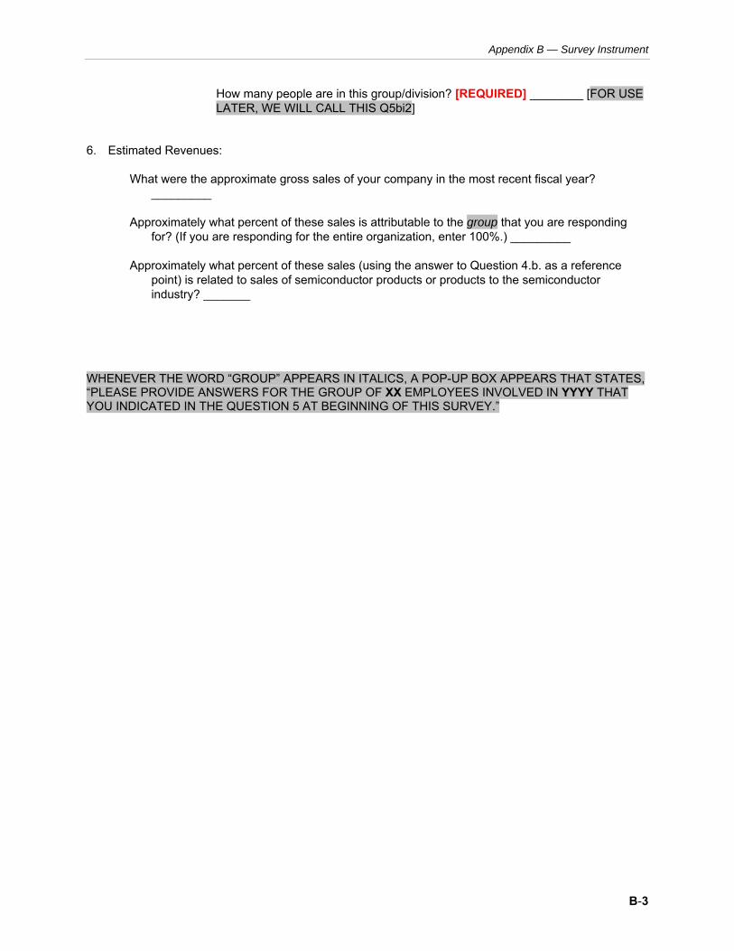
_________
Appendix B — Survey Instrument
How many people are in this group/division? [REQUIRED] ________ [FOR USE LATER, WE WILL CALL THIS Q5bi2]
6. Estimated Revenues:
What were the approximate gross sales of your company in the most recent fiscal year?
Approximately what percent of these sales is attributable to the group that you are responding for? (If you are responding for the entire organization, enter 100%.) _________
Approximately what percent of these sales (using the answer to Question 4.b. as a reference point) is related to sales of semiconductor products or products to the semiconductor industry? _______
WHENEVER THE WORD “GROUP” APPEARS IN ITALICS, A POP-UP BOX APPEARS THAT STATES, “PLEASE PROVIDE ANSWERS FOR THE GROUP OF XX EMPLOYEES INVOLVED IN YYYY THAT YOU INDICATED IN THE QUESTION 5 AT BEGINNING OF THIS SURVEY.”
B-3
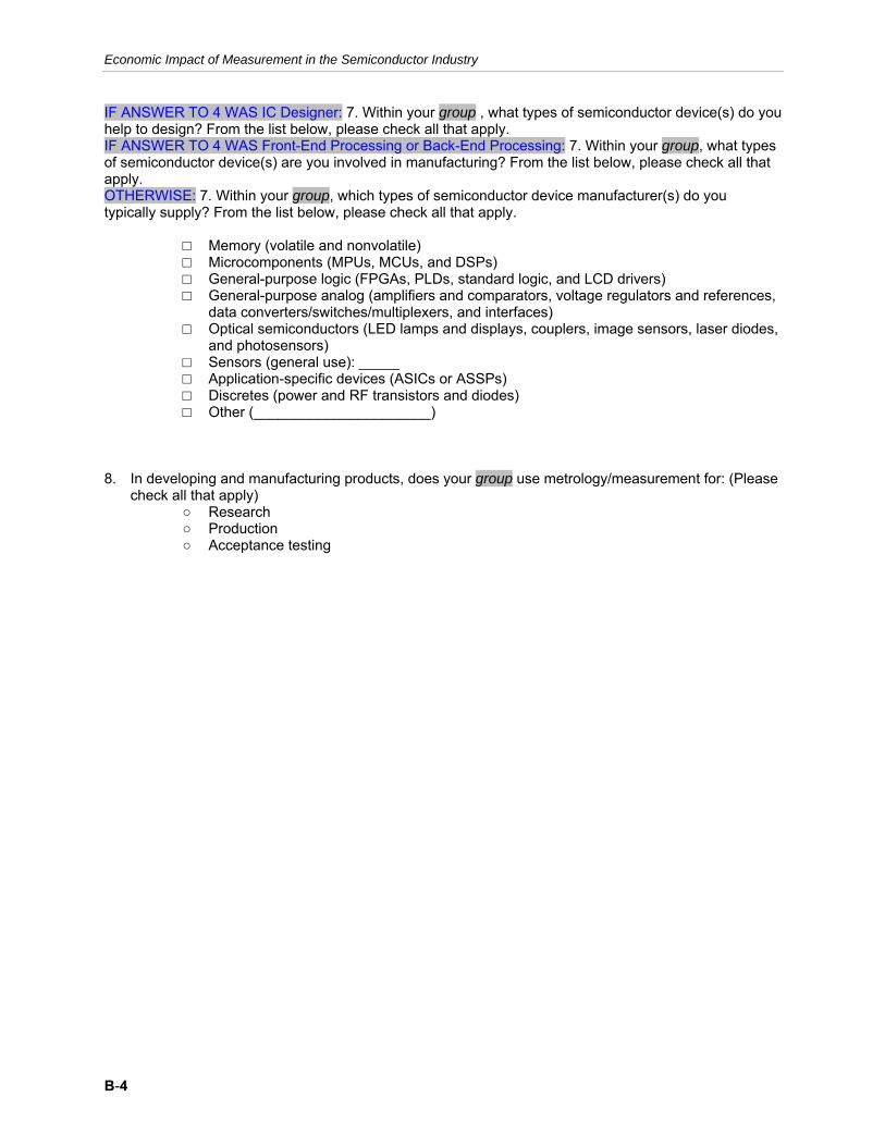
Economic Impact of Measurement in the Semiconductor Industry
IF ANSWER TO 4 WAS IC Designer: 7. Within your group , what types of semiconductor device(s) do you help to design? From the list below, please check all that apply. IF ANSWER TO 4 WAS Front-End Processing or Back-End Processing: 7. Within your group, what types of semiconductor device(s) are you involved in manufacturing? From the list below, please check all that apply. OTHERWISE: 7. Within your group, which types of semiconductor device manufacturer(s) do you typically supply? From the list below, please check all that apply.
□ Memory (volatile and nonvolatile) □ Microcomponents (MPUs, MCUs, and DSPs) □ General-purpose logic (FPGAs, PLDs, standard logic, and LCD drivers) □ General-purpose analog (amplifiers and comparators, voltage regulators and references,
data converters/switches/multiplexers, and interfaces) □ Optical semiconductors (LED lamps and displays, couplers, image sensors, laser diodes,
and photosensors) □ Sensors (general use): _____ □ Application-specific devices (ASICs or ASSPs) □ Discretes (power and RF transistors and diodes) □ Other (______________________)
8. In developing and manufacturing products, does your group use metrology/measurement for: (Please check all that apply)
○ Research ○ Production ○ Acceptance testing
B-4
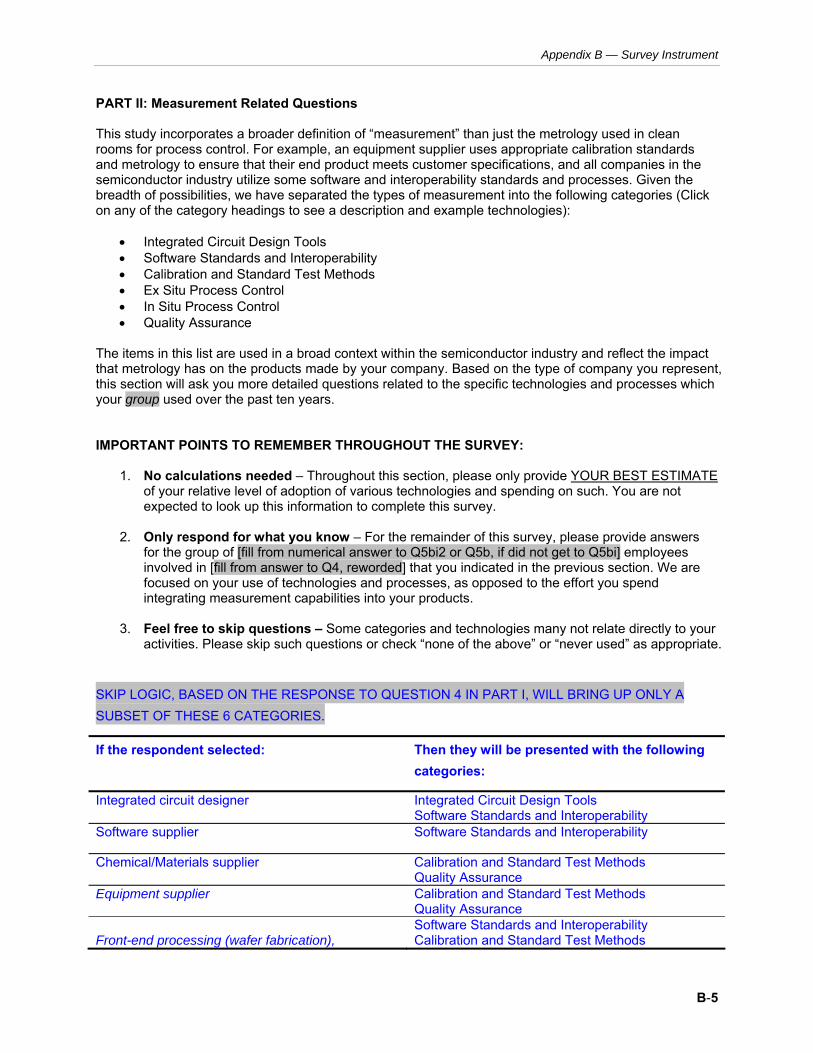
Appendix B — Survey Instrument
PART II: Measurement Related Questions
This study incorporates a broader definition of “measurement” than just the metrology used in clean rooms for process control. For example, an equipment supplier uses appropriate calibration standards and metrology to ensure that their end product meets customer specifications, and all companies in the semiconductor industry utilize some software and interoperability standards and processes. Given the breadth of possibilities, we have separated the types of measurement into the following categories (Click on any of the category headings to see a description and example technologies):
• Integrated Circuit Design Tools • Software Standards and Interoperability • Calibration and Standard Test Methods • Ex Situ Process Control • In Situ Process Control • Quality Assurance
The items in this list are used in a broad context within the semiconductor industry and reflect the impact that metrology has on the products made by your company. Based on the type of company you represent, this section will ask you more detailed questions related to the specific technologies and processes which your group used over the past ten years.
IMPORTANT POINTS TO REMEMBER THROUGHOUT THE SURVEY:
1. No calculations needed – Throughout this section, please only provide YOUR BEST ESTIMATE of your relative level of adoption of various technologies and spending on such. You are not expected to look up this information to complete this survey.
2. Only respond for what you know – For the remainder of this survey, please provide answers for the group of [fill from numerical answer to Q5bi2 or Q5b, if did not get to Q5bi] employees involved in [fill from answer to Q4, reworded] that you indicated in the previous section. We are focused on your use of technologies and processes, as opposed to the effort you spend integrating measurement capabilities into your products.
3. Feel free to skip questions – Some categories and technologies many not relate directly to your activities. Please skip such questions or check “none of the above” or “never used” as appropriate.
SKIP LOGIC, BASED ON THE RESPONSE TO QUESTION 4 IN PART I, WILL BRING UP ONLY A SUBSET OF THESE 6 CATEGORIES.
If the respondent selected: Then they will be presented with the following categories:
Integrated circuit designer Integrated Circuit Design Tools Software Standards and Interoperability
Software supplier Software Standards and Interoperability
Chemical/Materials supplier Calibration and Standard Test Methods Quality Assurance
Equipment supplier Calibration and Standard Test Methods Quality Assurance Software Standards and Interoperability
Front-end processing (wafer fabrication), Calibration and Standard Test Methods
B-5

Economic Impact of Measurement in the Semiconductor Industry
OR Ex Situ Process Control Back-end processing (packaging, assembly, and In Situ Process Control test) Quality Assurance
DESCRIPTION OF THE SIX CATEGORIES [THESE WILL COME UP AS EXPANDABLE TEXT FOR PARTICIPANTS TO VIEW A DESCRIPTION, BUT OTHERWISE WILL BE HIDDEN – THIS WILL APPEAR AS “CLICKABLE” LINKS IN LIST ABOVE AND HEADINGS ABOVE EACH TECHNOLOGY TABLE THAT FOLLOWS]:
1. Integrated Circuit Design Tools: This category includes modeling software and other tools and techniques used to aid integrated circuit design. These products utilize advanced measurement techniques and increasingly are coupled with the full range of metrology capabilities used in the semiconductor manufacturing process and help to define what should be measured.
Examples:
Electronic Design Automation (e.g., Mentor Graphics, Cadence, Agilent)
Circuit and Electromagnetic Simulators (e.g., SPICE, Ansoft Nexxim, Agilent)
Design for Manufacturing (e.g., Mentor Graphics Calibre, Agilent ADS, HPL Technologies, KLA– Tencor ProLith)
Electronic System-Level (ESL) tools (e.g., Cadence, Verity, Synopsis)
Process Simulation Tools (e.g., Silvaco ATHENA, Mathworks Matlab/Simulink)
Product Lifecycle Management (e.g., PTC Pro/ENGINEER)
2. Software Standards and Interoperability: This category includes standards, procedures, and tools that enable communication between organizations. Uniform software exchange standards are needed for the efficient exchange of designs. Further, organizations rely on the interoperability of measurement data among internal databases and equipment in order to allow efficient operations.
Examples:
Verification languages (e.g., Verilog, VHDL, SystemVerilog, SystemC)
Standard information exchange formats (e.g., IGES, STEP, GDSII)
3. Calibration and Standard Test Methods: This category involves the calibration of machinery and the use of standard testing procedures to ensure the accuracy and precision of processes and measurements. This category encompasses the use of reference materials, including those produced or certified by NIST or produced under the supervision of other recognized standards developing bodies, such as ASTM. Testing equipment must also be calibrated to ensure that temperature and electrical readings are accurate and defects are detected when present. This category also includes linear distance standards and equipment/processes used to ensure precise factory automation.
B-6
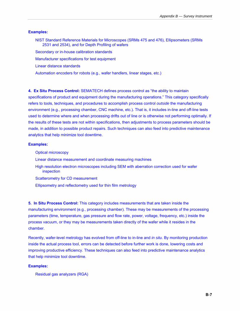
Appendix B — Survey Instrument
Examples:
NIST Standard Reference Materials for Microscopes (SRMs 475 and 476), Ellipsometers (SRMs 2531 and 2534), and for Depth Profiling of wafers
Secondary or in-house calibration standards
Manufacturer specifications for test equipment
Linear distance standards
Automation encoders for robots (e.g., wafer handlers, linear stages, etc.)
4. Ex Situ Process Control: SEMATECH defines process control as “the ability to maintain specifications of product and equipment during the manufacturing operations.” This category specifically refers to tools, techniques, and procedures to accomplish process control outside the manufacturing environment (e.g., processing chamber, CNC machine, etc.). That is, it includes in-line and off-line tests used to determine where and when processing drifts out of line or is otherwise not performing optimally. If the results of these tests are not within specifications, then adjustments to process parameters should be made, in addition to possible product repairs. Such techniques can also feed into predictive maintenance analytics that help minimize tool downtime.
Examples:
Optical microscopy
Linear distance measurement and coordinate measuring machines
High resolution electron microscopes including SEM with aberration correction used for wafer inspection
Scatterometry for CD measurement
Ellipsometry and reflectometry used for thin film metrology
5. In Situ Process Control: This category includes measurements that are taken inside the manufacturing environment (e.g., processing chamber). These may be measurements of the processing parameters (time, temperature, gas pressure and flow rate, power, voltage, frequency, etc.) inside the process vacuum, or they may be measurements taken directly of the wafer while it resides in the chamber.
Recently, wafer-level metrology has evolved from off-line to in-line and in situ. By monitoring production inside the actual process tool, errors can be detected before further work is done, lowering costs and improving productive efficiency. These techniques can also feed into predictive maintenance analytics that help minimize tool downtime.
Examples:
Residual gas analyzers (RGA)
B-7
Economic Impact of Measurement in the Semiconductor Industry
Plasma process monitors
Real-time plating bath chemistry monitors
Exposure meters
Optical strain measurements
Measurements of current or voltage
6. Quality Assurance: This category includes tests of starting materials and finished products at relevant points in the industry value chain (i.e., suppliers, wafer back-end, electronics packaging, etc.) to ensure that there are no defects. This category encompasses processes to ensure that: (1) the starting materials used in wafer fabs are of the right concentration, purity, and form, (2) wafers of integrated circuits will operate as expected, and (3) individual packaged integrated circuits will meet end product specifications.
Examples:
Resistivity testing (four-point probe, automation through CDE ResMap) of films and materials
Electrical testing (of equipment, assemblies, wafers, or other products)
Vibration, shock, and thermal cycling tests
Accelerated life testing/environmental testing
Optical and X-ray examination to identify surface defects or to measure adherence to customer specifications
X-ray examination, acoustical microscopy, or other methods to identify hidden defects
B-8
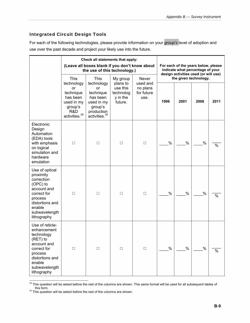
Appendix B — Survey Instrument
Integrated Circuit Design Tools
For each of the following technologies, please provide information on your group’s level of adoption and use over the past decade and project your likely use into the future.
Check all statements that apply: (Leave all boxes blank if you don’t know about
the use of this technology.) For each of the years below, please
indicate what percentage of your design activities used (or will use)
the given technology. This technology
or technique has been
used in my group’s
R&D activities.29
This technology
or technique has been
used in my group’s
production activities.30
My group plans to use this
technolog y in the future.
Never used and no plans for future
use. 1996 2001 2006 2011
Electronic Design Automation (EDA) tools with emphasis on logical simulation and hardware emulation
□ □ □ □ ____% ____% ____% ____ %
Use of optical proximity correction (OPC) to account and correct for process distortions and enable subwavelength lithography
□ □ □ □ ____% ____% ____% ____ %
Use of reticle-enhancement technology (RET) to account and correct for process distortions and enable subwavelength lithography
□ □ □ □ ____% ____% ____% ____ %
29 This question will be asked before the rest of the columns are shown. This same format will be used for all subsequent tables of this form.
30 This question will be asked before the rest of the columns are shown.
B-9

____________________________________________________________________________________ ____________________________________________________________________________________ ____________________________________________________________________________________
Economic Impact of Measurement in the Semiconductor Industry
Mixed analog and digital circuit simulation (e.g., HSPICE, Spectre, Eldo, SmartSpice, Pspice)
□ □ □ □ ____% ____% ____% ____ %
Comments: __________________________________________________________________________
In 2005, approximately what percentage of annual sales did your group invest in Integrated Circuit Design Tools? Please include investments in capital equipment, as well as spending on R&D and operating expenses.
○ ______ percent of annual sales.
○ Don’t know or prefer not to answer.
Over the past 10 years, has your group increased or decreased the dollar amount spent on Integrated Circuit Design Tools? Please indicate the approximate percentage as appropriate, or leave the space blank if you don’t know or prefer not to give a percentage figure.
○ Increased by ______ percent since 1996.
○ Decreased by ______ percent since 1996.
○ Maintained current level of spending.
○ Don’t know or prefer not to answer.
Over the next 5 years, does your group intend to increase or decrease the dollar amount spent on Integrated Circuit Design Tools? Please indicate the approximate percentage as appropriate, or leave the space blank if you don’t know or prefer not to give a percentage figure.
○ Increase by ______ percent by 2011.
○ Decrease by ______ percent by 2011.
○ Maintain current level of spending.
○ Don’t know or prefer not to answer.
B-10
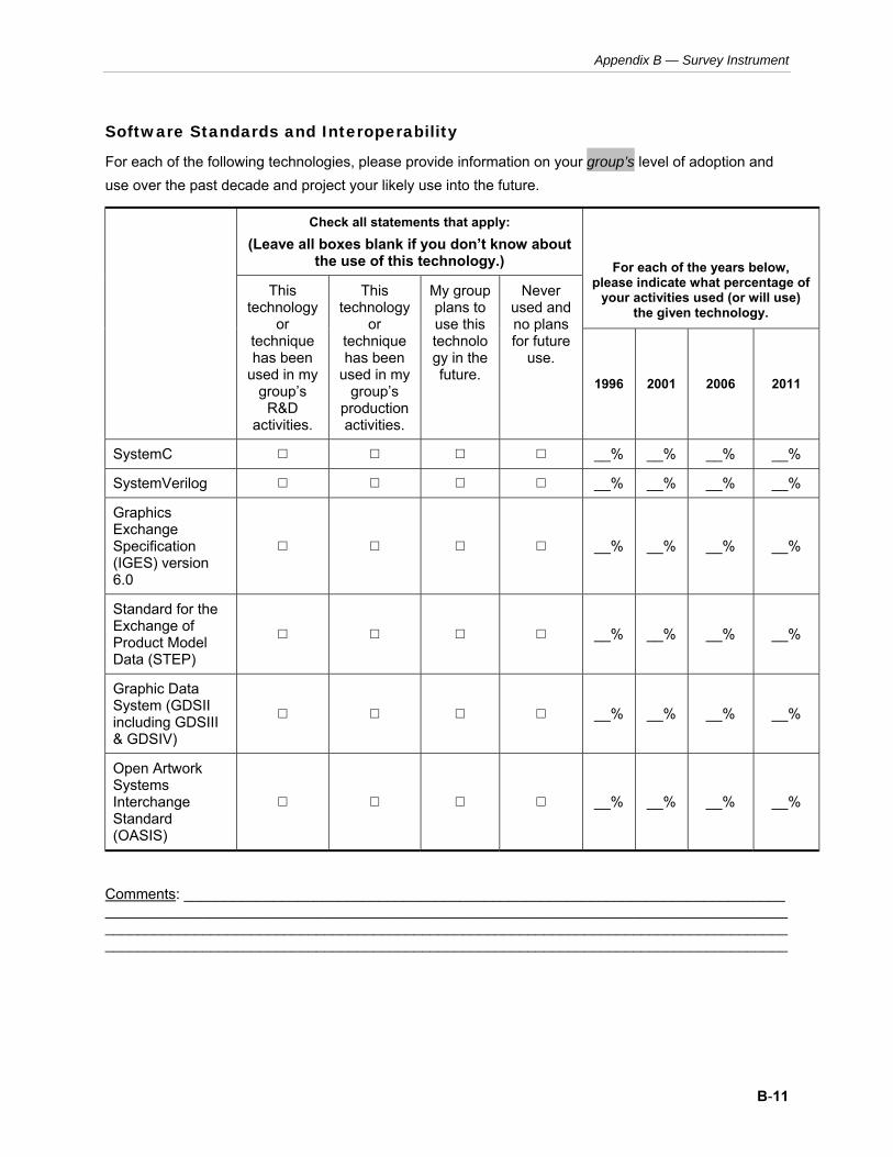
____________________________________________________________________________________ ____________________________________________________________________________________ ____________________________________________________________________________________
Appendix B — Survey Instrument
Software Standards and Interoperability
For each of the following technologies, please provide information on your group’s level of adoption and use over the past decade and project your likely use into the future.
Check all statements that apply: (Leave all boxes blank if you don’t know about
the use of this technology.) For each of the years below, please indicate what percentage of
your activities used (or will use) the given technology.
This technology
or technique has been
used in my group’s
R&D activities.
This technology
or technique has been
used in my group’s
production activities.
My group plans to use this technolo gy in the future.
Never used and no plans for future
use.
1996 2001 2006 2011
SystemC □ □ □ □ __% __% __% __%
SystemVerilog □ □ □ □ __% __% __% __%
Graphics Exchange Specification (IGES) version 6.0
□ □ □ □ __% __% __% __%
Standard for the Exchange of Product Model Data (STEP)
□ □ □ □ __% __% __% __%
Graphic Data System (GDSII including GDSIII & GDSIV)
□ □ □ □ __% __% __% __%
Open Artwork Systems Interchange Standard (OASIS)
□ □ □ □ __% __% __% __%
Comments: __________________________________________________________________________
B-11

Economic Impact of Measurement in the Semiconductor Industry
In 2005, approximately what percentage of annual sales did your group invest in Software Standards and Interoperability, whether in terms of investment in developing standards, products, or implementation? Please include investments in capital equipment, as well as spending on R&D and operating expenses.
○ ______ percent of annual sales.
○ Don’t know or prefer not to answer.
Over the past 10 years, has your group increased or decreased the dollar amount spent on Software Standards and Interoperability? Please indicate the approximate percentage as appropriate, or leave the space blank if you don’t know or prefer not to give a percentage figure.
○ Increased by ______ percent since 1996.
○ Decreased by ______ percent since 1996.
○ Maintained current level of spending.
○ Don’t know or prefer not to answer.
Over the next 5 years, does your group intend to increase or decrease the dollar amount spent on Software Standards and Interoperability? Please indicate the approximate percentage as appropriate, or leave the space blank if you don’t know or prefer not to give a percentage figure.
○ Increase by ______ percent by 2011.
○ Decrease by ______ percent by 2011.
○ Maintain current level of spending.
○ Don’t know or prefer not to answer.
B-12

Appendix B — Survey Instrument
Calibration and Standard Test Methods
For each of the following technologies, please provide information on your group’s level of adoption and use over the past decade and project your likely use into the future.
Check all statements that apply: (Leave all boxes blank if you don’t know about
the use of this technology.) For each of the years below, please indicate what
percentage of your product equipment calibration
activities used (or will use) the given technology.
This technology
or technique has been
used in my group’s
R&D activities.
This technology or
technique has been
used in my group’s
production activities.
My group plans to use this technolo gy in the future.
Never used
and no plans for
future use.
1996 2001 2006 2011
Reference materials (including NIST SRMs and NIST traceable reference materials (NTRM)) for high purity chemicals, gases, and solid materials
□ □ □ □ __% __% __% __%
Other reference materials (including NIST SRMs and NTRMs) for resistivity, particle count, thickness or other measurements
□ □ □ □ __% __% __% __%
NIST calibrated or NIST traceable power supplies, current supplies, or other electronics
□ □ □ □ __% __% __% __%
Linear distance standards with minimum linewidths of ~250 nm
□ □ □ □ __% __% __% __%
B-13

____________________________________________________________________________________ ____________________________________________________________________________________ ____________________________________________________________________________________
Economic Impact of Measurement in the Semiconductor Industry
Linear distance standards with sub-40 nm linewidths
□ □ □ □ __% __% __% __%
High resolution, high repeatability optical and magnetic encoders for factory automation including wafer handlers
□ □ □ □ __% __% __% __%
Comments: __________________________________________________________________________
In 2005, approximately what percentage of annual sales did your group invest in Production Equipment Calibration for Precision and Accuracy? Please include investments in capital equipment, as well as spending on R&D and operating expenses.
○ ______ percent of annual sales.
○ Don’t know or prefer not to answer.
Over the past 10 years, has your group increased or decreased the dollar amount spent on Production Equipment Calibration for Precision and Accuracy? Please indicate the approximate percentage as appropriate, or leave the space blank if you don’t know or prefer not to give a percentage figure.
○ Increased by ______ percent since 1996.
○ Decreased by ______ percent since 1996.
○ Maintained current level of spending.
○ Don’t know or prefer not to answer.
Over the next 5 years, does your organization intend to increase or decrease the dollar amount spent on Production Equipment Calibration for group and Accuracy? Please indicate the approximate percentage as appropriate, or leave the space blank if you don’t know or prefer not to give a percentage figure.
○ Increase by ______ percent by 2011.
○ Decrease by ______ percent by 2011.
○ Maintain current level of spending.
○ Don’t know or prefer not to answer.
B-14
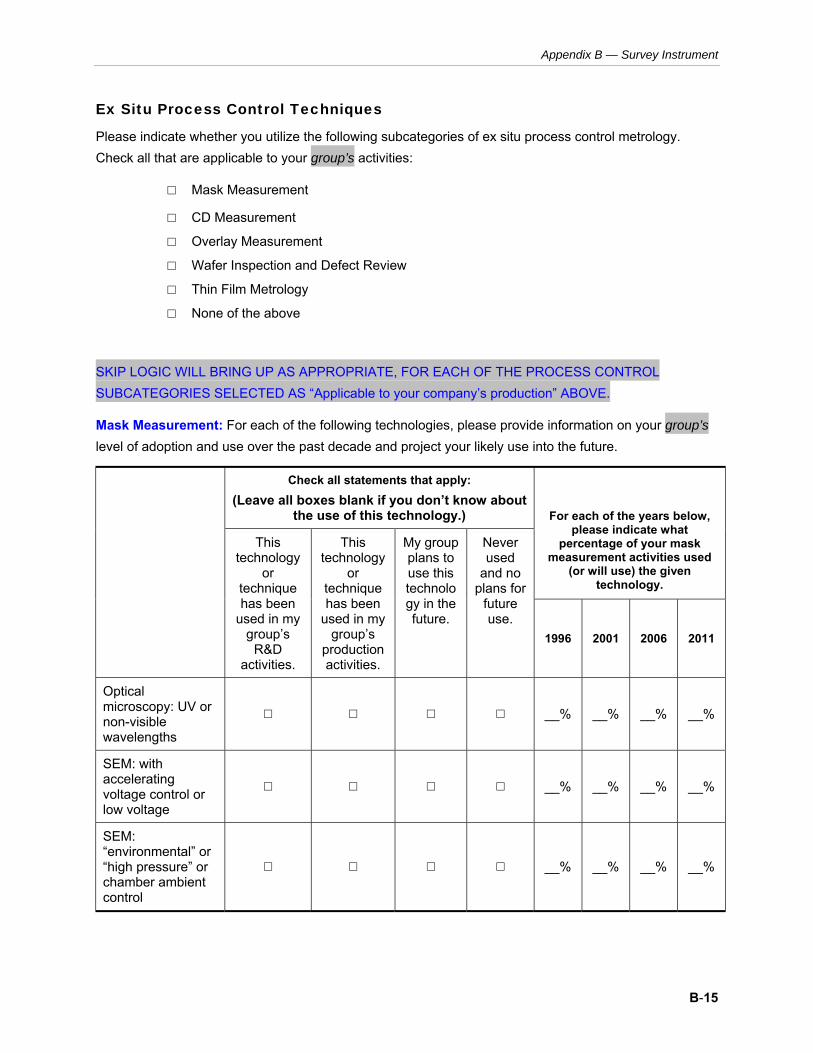
Appendix B — Survey Instrument
Ex Situ Process Control Techniques
Please indicate whether you utilize the following subcategories of ex situ process control metrology. Check all that are applicable to your group’s activities:
□ Mask Measurement
□ CD Measurement
□ Overlay Measurement
□ Wafer Inspection and Defect Review
□ Thin Film Metrology
□ None of the above
SKIP LOGIC WILL BRING UP AS APPROPRIATE, FOR EACH OF THE PROCESS CONTROL SUBCATEGORIES SELECTED AS “Applicable to your company’s production” ABOVE.
Mask Measurement: For each of the following technologies, please provide information on your group’s level of adoption and use over the past decade and project your likely use into the future.
Check all statements that apply: (Leave all boxes blank if you don’t know about
the use of this technology.) For each of the years below, please indicate what
percentage of your mask measurement activities used
(or will use) the given technology.
This technology
or technique has been
used in my group’s
R&D activities.
This technology
or technique has been
used in my group’s
production activities.
My group plans to use this technolo gy in the future.
Never used
and no plans for
future use.
1996 2001 2006 2011
Optical microscopy: UV or non-visible wavelengths
□ □ □ □ __% __% __% __%
SEM: with accelerating voltage control or low voltage
□ □ □ □ __% __% __% __%
SEM: “environmental” or “high pressure” or chamber ambient control
□ □ □ □ __% __% __% __%
B-15

____________________________________________________________________________________ ____________________________________________________________________________________ ____________________________________________________________________________________
____________________________________________________________________________________ ____________________________________________________________________________________ ____________________________________________________________________________________
Economic Impact of Measurement in the Semiconductor Industry
Comments: __________________________________________________________________________
CD Measurement: For each of the following technologies, please provide information on your group’s level of adoption and use over the past decade and project your likely use into the future.
Check all statements that apply: (Leave all boxes blank if you don’t know about
the use of this technology.) For each of the years below, please indicate what
percentage of your CD measurement activities used
(or will use) the given technology.
This technology
or technique has been
used in my group’s
R&D activities.
This technology
or technique has been
used in my group’s
production activities.
My group plans to use this technolo gy in the future.
Never used and no plans for future
use.
1996 2001 2006 2011
Optical microscopy: UV or non-visible wavelengths
□ □ □ □ __% __% __% __%
Optical scattering: scatterometry □ □ □ □ __% __% __% __%
SEM: with accelerating voltage control or low voltage
□ □ □ □ __% __% __% __%
SEM: in any configuration with aberration correction
□ □ □ □ __% __% __% __%
TEM: in any configuration □ □ □ □ __% __% __% __%
Comments: __________________________________________________________________________
B-16

____________________________________________________________________________________ ____________________________________________________________________________________ ____________________________________________________________________________________
Appendix B — Survey Instrument
Overlay Measurement: For each of the following technologies, please provide information on your group’s level of adoption and use over the past decade and project your likely use into the future.
Check all statements that apply: (Leave all boxes blank if you don’t know about
the use of this technology.) For each of the years below,
please indicate what percentage of your overlay
measurement activities used (or will use) the given technology.
This technology
or technique has been
used in my group’s
R&D activities.
This technology
or technique has been
used in my group’s
production activities.
My group plans to use this technolo gy in the future.
Never used and no plans for future
use.
1996 2001 2006 2011
Optical microscopy: with box targets and UV or non-visible wavelengths
□ □ □ □ __% __% __% __%
Optical microscopy: with targets other than box-in-box, any wavelengths
□ □ □ □ __% __% __% __%
Optical scattering or diffraction with grating targets
□ □ □ □ __% __% __% __%
Comments: __________________________________________________________________________
B-17
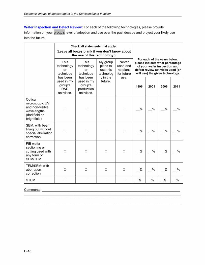
____________________________________________________________________________________ ____________________________________________________________________________________ ____________________________________________________________________________________
Economic Impact of Measurement in the Semiconductor Industry
Wafer Inspection and Defect Review: For each of the following technologies, please provide information on your group’s level of adoption and use over the past decade and project your likely use into the future.
Check all statements that apply: (Leave all boxes blank if you don’t know about
the use of this technology.) For each of the years below,
please indicate what percentage of your wafer inspection and
defect review activities used (or will use) the given technology.
This technology
or technique has been
used in my group’s
R&D activities.
This technology
or technique has been
used in my group’s
production activities.
My group plans to use this
technolog y in the future.
Never used and no plans for future
use.
1996 2001 2006 2011
Optical microscopy: UV and non-visible wavelengths (darkfield or brightfield)
□ □ □ □ __% __% __% __%
SEM: with beam tilting but without special aberration correction
□ □ □ □ __% __% __% __%
FIB wafer sectioning or cutting used with any form of SEM/TEM
□ □ □ □ __% __% __% __%
TEM/SEM: with aberration correction
□ □ □ □ __% __% __% __%
STEM □ □ □ □ __% __% __% __%
Comments: __________________________________________________________________________
B-18
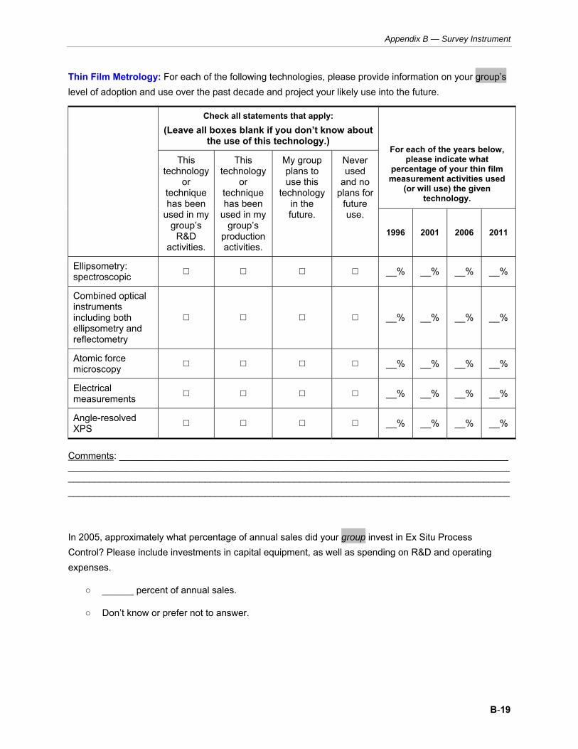
____________________________________________________________________________________ ____________________________________________________________________________________ ____________________________________________________________________________________
Appendix B — Survey Instrument
Thin Film Metrology: For each of the following technologies, please provide information on your group’s level of adoption and use over the past decade and project your likely use into the future.
Check all statements that apply: (Leave all boxes blank if you don’t know about
the use of this technology.) For each of the years below,
please indicate what percentage of your thin film measurement activities used
(or will use) the given technology.
This technology
or technique has been
used in my group’s
R&D activities.
This technology
or technique has been
used in my group’s
production activities.
My group plans to use this
technology in the future.
Never used
and no plans for
future use.
1996 2001 2006 2011
Ellipsometry: spectroscopic □ □ □ □ __% __% __% __%
Combined optical instruments including both ellipsometry and reflectometry
□ □ □ □ __% __% __% __%
Atomic force microscopy □ □ □ □ __% __% __% __%
Electrical measurements □ □ □ □ __% __% __% __%
Angle-resolved XPS □ □ □ □ __% __% __% __%
Comments: __________________________________________________________________________
In 2005, approximately what percentage of annual sales did your group invest in Ex Situ Process Control? Please include investments in capital equipment, as well as spending on R&D and operating expenses.
○ ______ percent of annual sales.
○ Don’t know or prefer not to answer.
B-19

Economic Impact of Measurement in the Semiconductor Industry
Over the past 10 years, has your group increased or decreased the dollar amount spent on Ex Situ Process Control? Please indicate the approximate percentage as appropriate, or leave the space blank if you don’t know or prefer not to give a percentage figure.
○ Increased by ______ percent since 1996.
○ Decreased by ______ percent since 1996.
○ Maintained current level of spending.
○ Don’t know or prefer not to answer.
Over the next 5 years, does your group intend to increase or decrease the dollar amount spent on Ex Situ Process Control? Please indicate the approximate percentage as appropriate, or leave the space blank if you don’t know or prefer not to give a percentage figure.
○ Increase by ______ percent by 2011.
○ Decrease by ______ percent by 2011.
○ Maintained current level of spending.
○ Don’t know or prefer not to answer.
In Situ Process Control Techniques
Please indicate whether you utilize the following subcategories of in situ process control metrology. Check all that are applicable to your group’s activities:
□ Processing Parameters and Process Vacuum Monitoring
□ Off-Wafer, In Situ Deposition Monitoring
□ On-Wafer, Deposition Monitoring and Endpoint Detection
□ None of the above
SKIP LOGIC WILL BRING UP AS APPROPRIATE, FOR EACH OF THE PROCESS CONTROL SUBCATEGORIES SELECTED AS “Applicable to your company’s production” ABOVE.
B-20
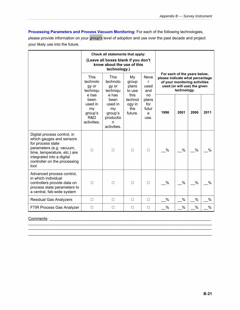
____________________________________________________________________________________ ____________________________________________________________________________________ ____________________________________________________________________________________
Appendix B — Survey Instrument
Processing Parameters and Process Vacuum Monitoring: For each of the following technologies, please provide information on your group’s level of adoption and use over the past decade and project your likely use into the future.
Check all statements that apply: (Leave all boxes blank if you don’t
know about the use of this technology.)
For each of the years below, please indicate what percentage
of your monitoring activities used (or will use) the given
technology.
This technolo
gy or techniqu
e has been
used in my
group’s R&D
activities.
This technolo
gy or techniqu
e has been
used in my
group’s productio
n activities.
My group plans to use
this technol ogy in
the future.
Neve r
used and no
plans for
futur e
use. 1996 2001 2006 2011
Digital process control, in which gauges and sensors for process state parameters (e.g. vacuum, time, temperature, etc.) are integrated into a digital controller on the processing tool
□ □ □ □ __% __% __% __%
Advanced process control, in which individual controllers provide data on process state parameters to a central, fab-wide system
□ □ □ □ __% __% __% __%
Residual Gas Analyzers □ □ □ □ __% __% __% __%
FTIR Process Gas Analyzer □ □ □ □ __% __% __% __%
Comments: __________________________________________________________________________
B-21
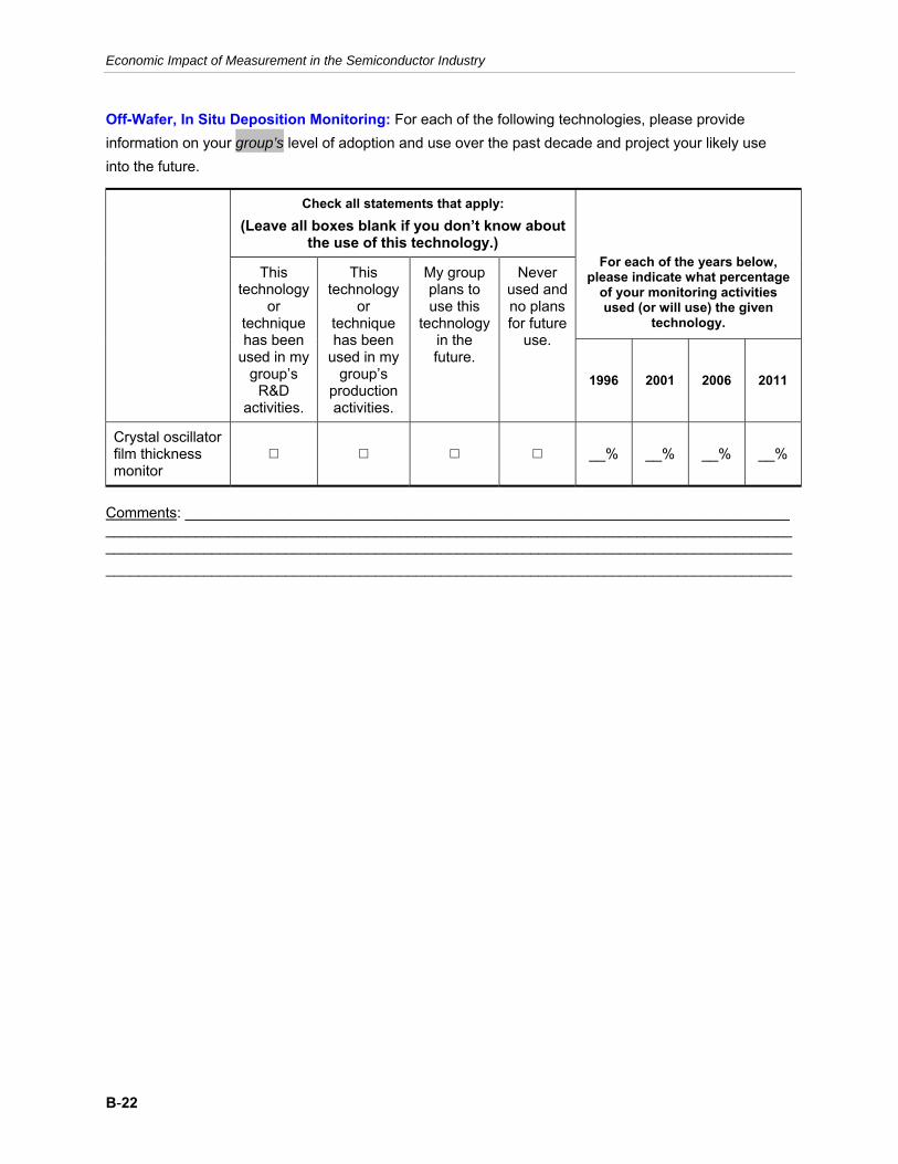
____________________________________________________________________________________ ____________________________________________________________________________________ ____________________________________________________________________________________
Economic Impact of Measurement in the Semiconductor Industry
Off-Wafer, In Situ Deposition Monitoring: For each of the following technologies, please provide information on your group’s level of adoption and use over the past decade and project your likely use into the future.
Check all statements that apply: (Leave all boxes blank if you don’t know about
the use of this technology.) For each of the years below,
please indicate what percentage of your monitoring activities used (or will use) the given
technology.
This technology
or technique has been
used in my group’s
R&D activities.
This technology
or technique has been
used in my group’s
production activities.
My group plans to use this
technology in the future.
Never used and no plans for future
use.
1996 2001 2006 2011
Crystal oscillator film thickness monitor
□ □ □ □ __% __% __% __%
Comments: __________________________________________________________________________
B-22
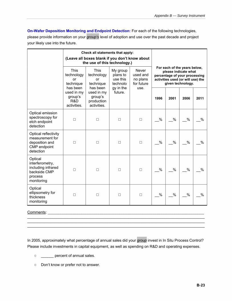
____________________________________________________________________________________ ____________________________________________________________________________________ ____________________________________________________________________________________
Appendix B — Survey Instrument
On-Wafer Deposition Monitoring and Endpoint Detection: For each of the following technologies, please provide information on your group’s level of adoption and use over the past decade and project your likely use into the future.
Check all statements that apply: (Leave all boxes blank if you don’t know about
the use of this technology.) For each of the years below,
please indicate what percentage of your processing activities used (or will use) the
given technology.
This technology
or technique has been
used in my group’s
R&D activities.
This technology
or technique has been
used in my group’s
production activities.
My group plans to use this technolo gy in the future.
Never used and no plans for future
use.
1996 2001 2006 2011
Optical emission spectroscopy for etch endpoint detection
□ □ □ □ __% __% __% __%
Optical reflectivity measurement for deposition and CMP endpoint detection
□ □ □ □ __% __% __% __%
Optical interferometry, including infrared backside CMP process monitoring
□ □ □ □ __% __% __% __%
Optical ellipsometry for thickness monitoring
□ □ □ □ __% __% __% __%
Comments: __________________________________________________________________________
In 2005, approximately what percentage of annual sales did your group invest in In Situ Process Control? Please include investments in capital equipment, as well as spending on R&D and operating expenses.
○ ______ percent of annual sales.
○ Don’t know or prefer not to answer.
B-23

Economic Impact of Measurement in the Semiconductor Industry
Over the past 10 years, has your group increased or decreased the dollar amount spent on In Situ Process Control? Please indicate the approximate percentage as appropriate, or leave the space blank if you don’t know or prefer not to give a percentage figure.
○ Increased by ______ percent since 1996.
○ Decreased by ______ percent since 1996.
○ Maintained current level of spending.
○ Don’t know or prefer not to answer.
Over the next 5 years, does your group intend to increase or decrease the dollar amount spent on In Situ Process Control? Please indicate the approximate percentage as appropriate, or leave the space blank if you don’t know or prefer not to give a percentage figure.
○ Increase by ______ percent by 2011.
○ Decrease by ______ percent by 2011.
○ Maintained current level of spending.
○ Don’t know or prefer not to answer.
B-24
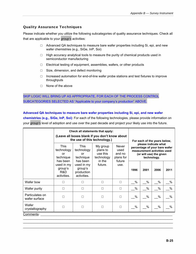
____________________________________________________________________________________ ____________________________________________________________________________________ ____________________________________________________________________________________
Appendix B — Survey Instrument
Quality Assurance Techniques
Please indicate whether you utilize the following subcategories of quality assurance techniques. Check all that are applicable to your group’s activities:
□ Advanced QA techniques to measure bare wafer properties including Si, epi, and new wafer chemistries (e.g., SiGe, InP, Soi)
□ High accuracy analytical tools to measure the purity of chemical products used in semiconductor manufacturing
□ Electrical testing of equipment, assemblies, wafers, or other products
□ Size, dimension, and defect monitoring
□ Increased automation for end-of-line wafer probe stations and test fixtures to improve throughputs
□ None of the above
SKIP LOGIC WILL BRING UP AS APPROPRIATE, FOR EACH OF THE PROCESS CONTROL SUBCATEGORIES SELECTED AS “Applicable to your company’s production” ABOVE.
Advanced QA techniques to measure bare wafer properties including Si, epi, and new wafer chemistries (e.g., SiGe, InP, Soi): For each of the following technologies, please provide information on your group’s level of adoption and use over the past decade and project your likely use into the future.
Check all statements that apply: (Leave all boxes blank if you don’t know about
the use of this technology.) For each of the years below, please indicate what
percentage of your bare wafer measurement activities used
(or will use) the given technology.
This technology
or technique has been
used in my group’s
R&D activities.
This technology
or technique has been
used in my group’s
production activities.
My group plans to use this
technology in the future.
Never used
and no plans for
future use.
1996 2001 2006 2011
Wafer bow □ □ □ □ __% __% __% __%
Wafer purity □ □ □ □ __% __% __% __%
Particulates on wafer surface □ □ □ □ __% __% __% __%
Wafer crystallography □ □ □ □ __% __% __% __%
Comments: __________________________________________________________________________
B-25
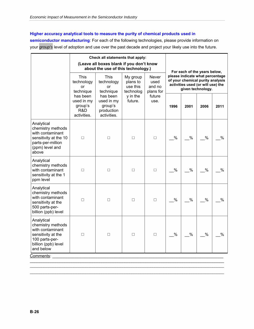
____________________________________________________________________________________ ____________________________________________________________________________________ ____________________________________________________________________________________
Economic Impact of Measurement in the Semiconductor Industry
Higher accuracy analytical tools to measure the purity of chemical products used in semiconductor manufacturing: For each of the following technologies, please provide information on your group’s level of adoption and use over the past decade and project your likely use into the future.
Check all statements that apply: (Leave all boxes blank if you don’t know
about the use of this technology.) For each of the years below,
please indicate what percentage of your chemical purity analysis activities used (or will use) the
given technology.
This technology
or technique has been
used in my group’s
R&D activities.
This technology
or technique has been
used in my group’s
production activities.
My group plans to use this
technolog y in the future.
Never used
and no plans for
future use.
1996 2001 2006 2011
Analytical chemistry methods with contaminant sensitivity at the 10 parts-per-million (ppm) level and above
□ □ □ □ __% __% __% __%
Analytical chemistry methods with contaminant sensitivity at the 1 ppm level
□ □ □ □ __% __% __% __%
Analytical chemistry methods with contaminant sensitivity at the 500 parts-per-billion (ppb) level
□ □ □ □ __% __% __% __%
Analytical chemistry methods with contaminant sensitivity at the 100 parts-per-billion (ppb) level and below
□ □ □ □ __% __% __% __%
Comments: __________________________________________________________________________
B-26
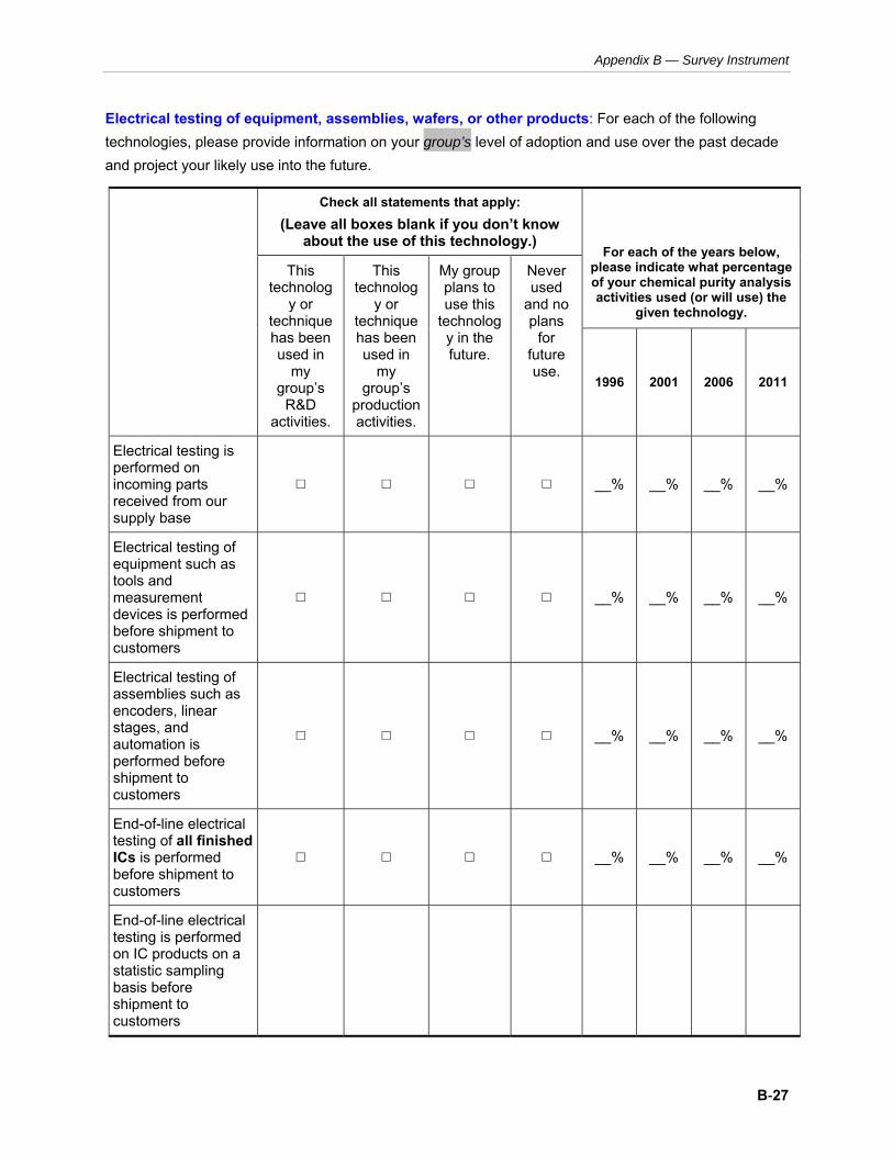
Appendix B — Survey Instrument
Electrical testing of equipment, assemblies, wafers, or other products: For each of the following technologies, please provide information on your group’s level of adoption and use over the past decade and project your likely use into the future.
Check all statements that apply: (Leave all boxes blank if you don’t know
about the use of this technology.) For each of the years below,
please indicate what percentage of your chemical purity analysis activities used (or will use) the
given technology.
This technolog
y or technique has been used in
my group’s
R&D activities.
This technolog
y or technique has been used in
my group’s
production activities.
My group plans to use this
technolog y in the future.
Never used
and no plans
for future use.
1996 2001 2006 2011
Electrical testing is performed on incoming parts received from our supply base
□ □ □ □ __% __% __% __%
Electrical testing of equipment such as tools and measurement devices is performed before shipment to customers
□ □ □ □ __% __% __% __%
Electrical testing of assemblies such as encoders, linear stages, and automation is performed before shipment to customers
□ □ □ □ __% __% __% __%
End-of-line electrical testing of all finished ICs is performed before shipment to customers
□ □ □ □ __% __% __% __%
End-of-line electrical testing is performed on IC products on a statistic sampling basis before shipment to customers
B-27
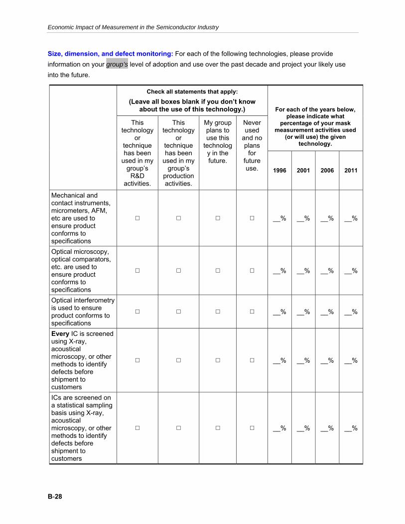
Economic Impact of Measurement in the Semiconductor Industry
Size, dimension, and defect monitoring: For each of the following technologies, please provide information on your group’s level of adoption and use over the past decade and project your likely use into the future.
Check all statements that apply: (Leave all boxes blank if you don’t know
about the use of this technology.) For each of the years below, please indicate what
percentage of your mask measurement activities used
(or will use) the given technology.
This technology
or technique has been
used in my group’s
R&D activities.
This technology
or technique has been
used in my group’s
production activities.
My group plans to use this
technolog y in the future.
Never used
and no plans
for future use. 1996 2001 2006 2011
Mechanical and contact instruments, micrometers, AFM, etc are used to ensure product conforms to specifications
□ □ □ □ __% __% __% __%
Optical microscopy, optical comparators, etc. are used to ensure product conforms to specifications
□ □ □ □ __% __% __% __%
Optical interferometry is used to ensure product conforms to specifications
□ □ □ □ __% __% __% __%
Every IC is screened using X-ray, acoustical microscopy, or other methods to identify defects before shipment to customers
□ □ □ □ __% __% __% __%
ICs are screened on a statistical sampling basis using X-ray, acoustical microscopy, or other methods to identify defects before shipment to customers
□ □ □ □ __% __% __% __%
B-28

____________________________________________________________________________________ ____________________________________________________________________________________ ____________________________________________________________________________________
Appendix B — Survey Instrument
Comments: __________________________________________________________________________
Increased automation for end-of-line wafer probe stations and test fixtures to improve throughputs: For each of the following technologies, please provide information on your group’s level of adoption and use over the past decade and project your likely use into the future.
Check all statements that apply: (Leave all boxes blank if you don’t know about
the use of this technology.) For each of the years below,
please indicate what percentage of your end-of-line wafer probe analysis activities used (or will
use) the given technology.
This technology
or technique has been
used in my group’s
R&D activities.
This technology
or technique has been
used in my group’s
production activities.
My group plans to use this
technology in the future.
Never used
and no plans
for future use. 1996 2001 2006 2011
Automated end-of-line (EOL) electrical testing of unpackaged die
□ □ □ □ __% __% __% __%
Automated end-of-line (EOL) electrical testing mainly for quad flat packs (QFP) and leaded chip carriers
□ □ □ □ __% __% __% __%
Automated end-of-line (EOL) electrical testing mainly for ball grid arrays (BGA) and plastic ball grid arrays (PBGA) chip carriers
□ □ □ □ __% __% __% __%
Automated end-of-line (EOL) testing mainly for flip-chip and chip-scale packaging (CSP) carriers
□ □ □ □ __% __% __% __%
B-29

____________________________________________________________________________________ ____________________________________________________________________________________ ____________________________________________________________________________________
Economic Impact of Measurement in the Semiconductor Industry
Comments: __________________________________________________________________________
Are you currently involved in acceptance testing in any of the following ways? Please check all that apply.
□ Our group qualifies or certifies vendors before purchasing inputs from them.
□ Our group conducts sample testing on each shipment of products from our suppliers.
□ Acceptance testing is performed by your customers on receipt.
Has this changed since 1996?
○ Yes, more today.
○ Yes, less today.
○ No, same as in 1996.
In 2005, approximately what percentage of annual revenues did your group invest in Quality Assurance Techniques? Please include investments in capital equipment, as well as spending on R&D and operating expenses.
○ ______ percent of annual sales.
○ Don’t know or prefer not to answer.
Over the past 10 years, has your group increased or decreased the dollar amount spent in Quality Assurance Techniques? Please indicate the approximate percentage as appropriate, or leave the space blank if you don’t know or prefer not to give a percentage figure.
○ Increased by ______ percent since 1996.
○ Decreased by ______ percent since 1996.
○ Maintained current level of spending.
○ Don’t know or prefer not to answer.
Over the next 5 years, does your group intend to increase or decrease the dollar amount spent on in Quality Assurance Techniques? Please indicate the approximate percentage as appropriate, or leave the space blank if you don’t know or prefer not to give a percentage figure.
○ Increase by ______ percent by 2011.
○ Decrease by ______ percent by 2011.
○ Maintained current level of spending.
○ Don’t know or prefer not to answer.
B-30

____________________________________________________________________________________ ____________________________________________________________________________________ ____________________________________________________________________________________ ____________________________________________________________________________________
Appendix B — Survey Instrument
THANK YOU
Thank you for completing the NIST/RTI Semiconductor Measurement Economic Impact Assessment Study. Based on your participation, we will be developing cost and benefit figures related to the adoption of measurement technologies and processes during the past ten years.
If you would like to be contacted when a final report is publicly available and/or if we can contact you with any questions we may have, please indicate such:
□ I am willing to have RTI contact me about my responses to this survey. □ Please send me a copy of the final report when it is available.
If you clicked either box above, please provide the following contact information and any additional comments or questions you would like to discuss with us (NOTE: your email address and contact information will not be shared with anyone outside RTI or used for any other purpose outside this project):
Name: _____________________________ Company Name: _____________________________ Email Address: _____________________________ Phone Number: _____________________________
Comments: __________________________________________________________________________
If you have any further questions, please contact RTI at [email protected]. Thank you.
NOTE: If you would like to fill-out the survey for another part of your business, please click on the following link: http://semimetrology.rti.org. Or if you would like to have a colleague fill out the survey out for their division, either forward them the email invitation you received or enter your name and email address above and enter their email address below, and an email will be sent to them with the survey material, indicating that you asked that it be sent to them.
Intended recipient’s email address: _____________________
B-31

Economic Impact of Measurement in the Semiconductor Industry
AT THE BOTTOM OF EACH PAGE, PARTICIPANTS WILL SEE A “NEXT”, “BACK”, AND “SAVE AND COME BACK LATER” BUTTONS. IF THEY SELECT “SAVE AND COME BACK LATER”, THEY WILL SEE THE FOLLOWING:
THANK YOU
Thank you for filling out part of this survey for the NIST/RTI Semiconductor Measurement Economic Impact Assessment Study. If you would be willing to come back and complete the survey at a later time, please create a user ID and password below:
User ID: ____________ Password: ____________
If you have any questions, please contact RTI at [email protected].
B-32