ecole de technologie superieure universite du quebec...
TRANSCRIPT

ECOLE DE TECHNOLOGIE SUPERIEURE UNIVERSITE DU QUEBEC
THESIS PRESENTED TO ECOLE DE TECHNOLOGIE SUPERIEUR E
IN PARTIAL FULLFILMENT OF THE REQUIREMENTS FOR THE DEGREE OF
MASTER OF ENGINEERING M. ENG.
BY ELZAYAT, Ahmed
DESIGN AND REALISATION OF FILTERS ON MHMIC AND MMIC FABRICATION PROCESSES FOR DUPLEXERS REALISATIO N
MONTREAL, MARCH 7, 2008
© Ahmed Elzayat , 2008
THIS THESIS HAS BEEN EVALUATED
BY THE FOLLOWING BOARD OF EXAMINERS:
M. Ammar B. Kouki, director Department of electrical engineering at the Ecole de technologic superieure
M. Christian Gargour, jury president Department of electrical engineering at the Ecole de technologic superieure
Vahe Nerguizian, jury member Department of electrical engineering at the Ecole de technologic superieure
THIS THESIS HAS BEEN PRESENTED AND DEFENDED
ON FEBRUARY, 6, 2008
AT ECOLE DE TECHNOLOGIE SUPERIEUR E

ACKNOWLEDGEMENTS
I woul d lik e first o f al l t o thank , m y mothe r fo r nourishin g th e sens e o f wonde r tha t go d
blessed m e with since I started to read abou t physics and science in general a t a quite young
age, m y fathe r fo r hi s mora l an d financial support , an d m y wif e fo r he r suppor t an d
understanding.
On th e professiona l leve l I would lik e t o than k Prof . Amma r Kouk i fo r hi s guidanc e an d
encouragement throug h m y work an d fo r hi s effor t i n elucidating some of the most difficul t
concepts in electromagnetics i n a clear concise way. Here 1 have to admit that his courses in
the Ecol e d e Technologi c Superieure , an d I have attende d al l o f them , wer e particularl y
inspiring.
Finally, I would like to extend my thanks to my colleagues in the LACIME laboratory for the
enriching discussions both on the scientific and personal levels.
Above al l I would lik e t o than k Alla h fo r givin g m e the patienc e an d th e perseveranc e t o
complete the work related to this dissertation through difficult time s in my life.

CONCEPTION E T REALISATIO N D E FILTRES SU R MHMI C MMI C E T PROCEDES D E FABRICATIO N POU R L A REALISATIO N D E DEPLEXEUR S
ELZAYAT, Ahme d
RESUME
Dans Fenvironnemen t actue l de s telecommunications , le s terminau x multi-mode s multi -bandes son t courammen t utilise s dan s le s systeme s d e communication s modemes . Ce s terminaux integren t plusieur s « front-ends » radio frequences (RF) , chacun pou r un e bande d e frequences, don t l e fonctionnemen t necessit e des filtres o u duplexeurs RF . En plus , les filtre s RF son t d e taille s relativemen t importante s pa r rappor t a d'autre s composant s RF . Pa r consequent, le s filtres e t le s duplexeur s occupen t un e parti e d e plu s e n plu s grand e dan s le s emetteurs-recepteurs modemes . Cec i a condui t l a communaut e scientifiqu e a consacre r plu s d*efforts a la miniaturisation de s filtres radiofrequences .
Le present travai l s'inscri t dan s c e contexte, dans u n effor t visan t a mettre a u poin t de s filtres et de s duplexeur s miniaturise s ayan t d e faible s perte s e t un e haut e isolation . C e memoir e presente un e topologi e d e filtres / duplexeur s miniaturise s base e su r un e techniqu e d e miniaturisation topologiqu e e n utilisan t Fanalys e e t la conceptio n assistee s pa r ordinateur . Les filtres con9u s dans c e travai l s'adapt e bie n a des precedes de fabricatio n e n technologie s planaires. Telle s qu e "Monolithi c Hybri d Microwav e Integrate d Circui t (MHMIC) " e t "Monolithic Microwav e Integrate d Circui t (MMIC)" . Ce s precedes on t et e choisi t a cause d e leurs caracteristique s d e miniaturisatio n e t d"integration . Le s filtres obtenu s montren t un e reducfion significativ e d e taill e pa r rappor t a Feta t d e Fart . L a techniqu e d e miniaturisatio n utilisee peu t etr e combine e ave c le s technologie s d e fabricatio n multicouche s e t d'autre s techniques avancee s d e fabricatio n pou r potentiellemen t abouti r a des filtres / duplexeur s d e tailles raisonnables pou r une integration monolithiques .

DESIGN AND REALISATION OF FILTERS ON MHMIC AND MMIC FABRICATION PROCESSE S FO R DUPLEXERS REALISATIO N
ELZAYAT, Ahmed
ABSTRACT
In the current telecommunicatio n environment , multimod e multiband terminal s ar e common place i n transceiver s architectures . Thes e terminal s integrat e severa l radi o frequenc y front -ends eac h fo r a differen t radi o frequenc y band . Prope r operatio n require s a separat e radi o frequency filter o r duplexe r fo r eac h band . I n addition t o this , filters are relatively larg e in size compared to other front-end components . Consequently, filters and duplexers occupy an increasing portio n o f mode m radi o frequenc y transceivers ' real-estate . Thi s ha s le d th e research community to dedicate more effort t o filter miniaturisation techniques.
This work subscribes to this context in an effort t o develop miniaturised filters and duplexers with lo w losse s an d hig h isolation . Thi s thesis present s a miniaturised topolog y base d o n a topological miniaturisatio n techniqu e usin g compute r aide d desig n an d analysis . The filters designed i n thi s wor k ar e suitabl e fo r manufacturin g o n an y plana r fabricatio n technolog y such a s Monolithi c Hybri d Microwav e Integrate d Circui t (MHMIC ) an d Monolithi c Microwave Integrate d Circui t (MMIC) . These specifi c processe s wer e selected an d used fo r fabrication becaus e of their high miniaturisation an d integration features . Th e realised filters show a significan t reductio n i n siz e compare d t o th e curren t stat e o f th e art . The propose d miniaturization technique , combine d wit h multilaye r fabricatio n technologie s an d othe r fabrication advancements , can potentially lead to filters and duplexers of reasonable sizes fo r monolithic integration.
TABLE O F CONTENT S
Page
INTRODUCTION 1 3
CHAPTER 1 R F FILTERS AN D DUPLEXER S I N MODERN WIRELES S SYSTEMS . 15 1.1 Introductio n 1 5
1.1.1 Plana r R F Filters 1 8 1.1.2 Duplexer s 2 0
1.2 Surve y of pertinent researc h activitie s 2 2 1.3 Conclusio n 2 5
CHAPTER 2 PRINCIPLE S O F COUPLED RESONATOR S FILTE R DESIG N 2 6 2.1 Introductio n 2 6 2.2 Desig n o f direct couple d resonato r band pas s filters 2 6
2.2.1 Derivatio n o f the equivalent circui t 2 8 2.2.2 Extractio n o f coupling coefficient s usin g electromagnetic simulatio n 3 3
2.2.2.1 Extracfin g o f coupling factorM 3 4 2.2.2.2 Extractin g of external qualit y factor^^ , 3 6
2.2.3 Transmissio n zero s at finite frequencie s 3 8 2.2.4 Couple d resonato r filter s wit h a single pair of transmission zero s 4 2
2.3 Conclusio n 4 5
CHAPTER 3 FILTER S AND DUPLEXER S I N MHMIC TECHNOLOG Y 4 6 3.1 Introducfio n 4 6 3.2 Th e Ay4±5 Resonator 4 8
3.2.1 Secon d orde r band-bass filters usin g X/4±8 resonator s 5 2 3.2.2 Symmetri c Fee d Stmctur e 5 2 3.2.3 Asymmetri c Fee d Stmctur e 5 6 3.2.4 Topologica l Optimizatio n 6 2 3.2.5 Modifie d por t stmctur e 6 7
3.3 Desig n o f miniaturised duplexer s 7 2 3.3.1 Fabricatio n result s on MHMIC proces s 7 4
3.3.1.1 Introductio n 7 4 3.3.1.2 Firs t Fabricatio n Ru n 7 5 3.3.1.3 Secon d Fabricatio n Ru n 7 8
3.4 Conclusio n 8 1
CHAPTER 4 FILTER S AN D DUPLEXER S O N MMI C TECHNOLOG Y 8 2 4.1 Introducfio n 8 2 4.2 Couple d resonato r filter desig n 8 3 4.3 Desig n o f miniaturised lumpe d element s filter 8 4

Vll
4.3.1 Idea l filter synthesis 8 5 4.3.2 Mode l with transmission line s 8 7 4.3.3 Assembl y and final optimisation 9 0
4.4 Conclusio n 9 2
CONCLUSION 9 3
BIBLIOGRAPHY 9 4

LIST OF TABLES
Page
Table 1. 1 A comparative table between the different approache s 2 4
Table 2.1 Th e values of the coupling coefficient M 3 5
Table 2.2 Th e values of the coupling coefficient Q^ 3 6
Table 3.1 Layer s arrangement of the default substrat e in this work 4 7
Table 3.2 Geometrica l and electrical characteristics of used transmission line 4 7
Table 3.3 Swee p range normalization for design parameter 6 1
Table 3.4 Symmetri c versus asymmetric feed response to parameter sweep 6 1
Table 4.1 Typica l stack up of a MMIC substrate 8 2
Table 4.2 Geometrica l an d electrical characteristics of a transmission line 8 3
LIST OF FIGURES
Page
Figure 1.1 A multi-mode front end module with emphasis on integrafion technologies 1 7
Figure 1.2 Duplexe r architecture 2 1
Figure 2.1 A general representafion of direct coupled resonators filter 2 7
Figure 2.2 Lo w pass prototype filter of Chebychev or maximally flat response 2 9
Figure 2.3 Lowpas s to Highpass Filter Transformation 2 9
Figure 2.4 Trasnforme d bandpas s fdter (Bottom) Circuit transformation 3 0
Figure 2.5 Conceptua l operafion o f immittance inverters 3 0
Figure 2.6 Step-by-ste p band pass section transformation 3 1
Figure 2.7 (Left ) Setu p for Q^ measurement (Rigth) Setup for AT measuremen t 3 4
Figure 2.8 Circui t Co-simulafion fo r determining coupling coefficient 3 5
Figure 2.9 Extractin g of the coupling coefficient betwee n two resonators 3 6
Figure 2.10 Circui t Co-simulation for determining extemal quality factor 3 7
Figure 2.11 Determinatio n of extemal quality factor 3 7
Figure 2.12 3rd . Order Chebychev filter at different frequencie s 3 9
Figure 2.13 Amplitud e response comparison between Chebychev and elliplitc filters 4 0
Figure 2.14 Circui t diagram for 3rd. order elliptic filter 4 1
Figure 2.15 Circui t elements providing transmission zeros 4 2
Figure 2.16 Lo w pass Chebychev prototype with poles at finite frequency [6] 4 3
Figure 2.17 Squar e loop coupled resonator filter with resonators cross coupling From[6]. ...44
Figure 2.18 Transmissio n response for filter in figure 2.17 above [6] 4 4
Figure3.1 Stmctureo f the /l/ 4 + t) resonato r (a) Theoretical model (b) Circuit model 4 8

X
Figure 3.2 LineCal c showing resonator loss as A DB 4 9
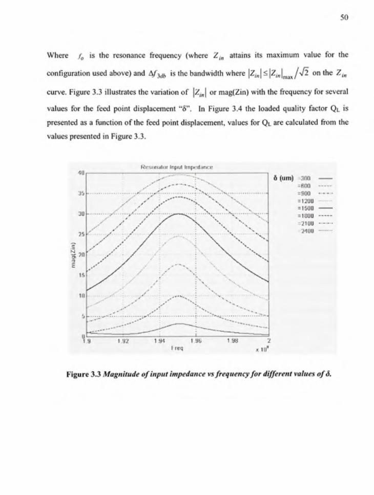
Figure 3.3 Magnitud e of input impedance vs frequency fo r different value s of 8 5 0
Figure 3.4 . Q i vs 8 5 1
Figure 3.5 Secon d order filter using AJAtS resonators in symmetric feed configuration 5 3
Figure 3.6 Typica l response for the symmetric feed point filter 5 3
Figure 3.7 Effec t o f X on Transmission (a) . Adaptation (b) and Zero location (c) 5 5
Figure 3.8 Effec t o f 8 on Transmission (a) . Adaptation (b) and Zero location (c) 5 6
Figure 3.9 Secon d order filter usingA./4±8 resonators in asymmetric feed configuration 5 7
Figure 3.10 Typica l response for the asymmetric feed point filter 5 7
Figure 3.11 Effec t o f 8 on Transmission (a) . Adaptation (b) and Zero location (c) 5 8
Figure 3.12 Effec t o f 8 on Zero location showing an unresolved zero 5 9
Figure 3.13 Effec t o f X on Transmission (a), Adaptafion (b ) and Zero locafion (c ) 6 0
Figure 3.14 Firs t iteration of topological opfimisafion 6 4
Figure 3.15 Transmissio n and return loss response of the topology in Figure 3.14 6 4
Figure 3.16 Respons e of the filter in response to parameters sweep 6 5
Figure 3.17 Geometricall y optimized stmcture 6 5
Figure 3.18 Transmissio n and return loss response of the topology in figure 3.17 6 6
Figure 3.19 3 Dimensional model in EMDS 6 7
Figure 3.20 Momentu m (2.5D) vs EMDS (3D) simulafion results 6 9
Figure 3.21 (Right ) the mesh used (Left) the poynting vector distribution a t 1.96GHz 6 9
Figure 3.22 Filte r topology with modified port s 7 0
Figure 3.23 Filte r response to variation of port width (Y) for the topology in figure 3.22. ...71
Figure 3.24 Filte r response of the topology in figure 3.22 7 1

XI
Figure 3.25 Classica l duplexe r stmctur e 7 2
Figure 3.2 6 Topologicall y optimize d duplexe r stmctur e 7 3
Figure 3.27 Optimise d duplexe r response (Left ) Retur n loss , (Right) Transmission 7 3
Figure 3.2 8 (Left ) Filte r (Right ) Duplexe r 7 6
Figure 3.29 Filte r measurement s (Transmission ) 7 6
Figure 3.30 Filte r measurement s (Retur n los s 7 7
Figure 3.31 Duplexer , Transmissio n (a) . Isolatio n (b ) and Retu m los s (c) 7 7
Figure 3.3 2 UMT S filters topologies . (Left ) Tx-filte r (Right ) Rx-filte r 7 8
Figure 3.33 UMT S Tx- filter fabrication . Transmission (a) , Retum los s (b) 7 9
Figure 3.34 UMT S R x filter fabricatio n Transmissio n (a) , Retum los s (b) 7 9
Figure 3.3 5 UMT S duplexe r topolog y 8 0
Figure 3.3 6 UMT S Duplexe r fabricafion : Transmissio n (a) , Isolafion (b ) Retum los s (c) . ...80
Figure 4.1 Preliminar y couple d resonato r filter o n MMIC substrat e 8 3
Figure 4.2 Electromagnefi c simulatio n result s of geometry presented i n figure 4. 1 8 4
Figure 4.3 Filte r design guid e window 8 6
Figure 4.4 Synthesise d ellipti c 3rd . order filter 8 6
Figure 4.5 Optimisatio n o f a filter section includin g transmissio n line s Q model 8 8
Figure 4.6 Layou t o f an optimised filter sectio n 8 9
Figure 4.7 UMT S Tx band lumpe d elemen t filter 9 0
Figure 4.8 UMT S T x ban d lumpe d elemen t filter- simulatio n result s 9 1
Figure 4.9 UMT S R x band filter 9 1
Figure 4.10 UMT S R x band filter - simulatio n result s 9 2

LIST O F ACRONYM S
ADS Advance d Desig n Syste m
BAW Bul k Acoustic Wav e
BiCMOS Bipola r Complementary Meta l Oxid e Transisto r
CPW Coplana r Wav e Guid e
FDD Frequenc y Divisio n Duple x
GaAs Galliu m Arsenid e
GSM Globa l Syste m fo r Mobil e communicatio n
HBT Hetero-juncfio n Bipola r Transisto r
LNA Lo w Noise Amplifie r
LTCC Lo w Temperature Co-fire d Ceramic s
MHMIC Microwav e Hybri d Monolithi c Integrate d Circui t
MMIC Microwav e Monolithi c Integrate d Circui t
MS MicroStri p
PA Powe r Amplifie r
pHEMT pseudomorphi c Hig h Electro n Mobilit y Transisto r
RF Radi o Frequenc y
SAW Surfac e Acousti c Wav e
TDD Tim e Division Duple x
UMTS Universa l Mobil e Telecommunication Syste m
WCDMA Wid e band Cod e Division Multipl e Acces s

INTRODUCTION
Motivation an d Backgroun d
On th e roa d t o ubiquitou s connectivity , th e wireles s telecommunicatio n industr y i s
witnessing a n unprecedente d deman d fo r multi-mod e multi-servic e wireles s use r terminals .
As manufacturer s tr y t o fulfil l thes e demands , majo r challenge s aris e causin g a n eve r
increasing difficult y i n thi s endeavour . Whil e manufacturer s ar e increasin g th e numbe r o f
circuits integrate d int o a terminal, the y ar e faced wit h th e insatiabl e deman d o f the consume r
to have lighter , smaller , an d cheaper terminals .
On th e othe r side , the coexistenc e o f a multitude o f wireles s standard s necessitate s excellen t
management o f the radio frequenc y resource s an d isolatio n betwee n differen t radi o frequenc y
bands.
Radio frequenc y filters an d duplexer s ar e th e come r stone s i n spectra l management , havin g
escaped miniaturizatio n trend s fo r a relativel y lon g time ; nowaday s the y ar e a t th e centr e
stage o f thes e trends . A s th e telecommunicatio n industr y i s experiencin g it s highes t growt h
rates i n th e mobil e sector , wher e th e frequenc y band s allocate d fo r thes e service s ar e
typically i n th e lowe r en d o f th e microwav e frequenc y ranges , miniaturisatio n i s no t a goo d
to have feature , i t becomes a pressing necessity . The difficulties encountere d i n miniaturisin g
these component s stem s fro m som e fundamenta l physica l an d technologica l limitations .
These limitation s ar e challengin g researcher s t o pus h th e limit s o f desig n technique s o r
fabrication technologie s o r both.
Our wor k subscrib e t o thi s general effor t o n the design techniqu e front . Th e design techniqu e
chosen i s tha t o f topologica l optimisatio n t o desig n miniatur e couple d resonato r filters i n
Microstrip stmctures . I t ha s th e advantag e tha t i t ca n benefi t from man y o f th e fabricafio n
technologies advancemen t i n the fijture.

14
Organization
The thesi s i s organized a s follows ; i n Chapte r 1 we wil l presen t a system overvie w o f th e
filters and duplexers in the context of multimode wireless systems. Then we introduce planar
coupled resonator s filters as a candidate approach fo r designing miniaturized R F filters. The
system characteristics of these filters are explained followed b y an introduction to the design
parameters o f these filters ; thos e being, quality factor , coupling , an d extema l qualit y factor .
We conclude by a literature survey of the state of the art, followed b y a brief comparison of
the results reported by different desig n approaches in open literature.
Chapter 2 will serv e as a theoretical introductio n fo r the design o f coupled resonato r filters.
We start with the introduction of direct coupled resonator filters and how to they synthesised
from low pass prototypes, then a theoretical introductio n o f the transmission zeros , and how
they are realised using coupled resonator .
In Chapte r 3 w e wil l presen t th e techniqu e employe d t o desig n miniaturize d filters an d
duplexers. W e star t b y presentin g th e /l/4±< 5 wavelengt h resonato r whic h i s th e basi c
resonator i n ou r work . Subsequently , th e resonato r wil l b e use d t o desig n tw o filtering
stmctures, the symmetric feed an d the non-symmetric feed . Usin g computer aided design and
analysis we will compare the two stmctures to choose a candidate for miniaturisation . Onc e
we hav e a candidat e stmctur e w e wil l appl y th e topologica l optimisatio n techniqu e t o
miniaturise th e filter. Finall y w e wil l presen t th e measuremen t o f filters an d duplexer s
fabricated vi a MHMIC process.
In Chapter 4 we will present th e results of filters designed usin g the technique introduced i n
chapter 3 and lumped elements ; both ar e designed targetin g a high en d MMI C process . The
target process is called TQPED. This MMIC process of TriQuint Semiconductor s is a process
where typically several elements of the RF front (ex. LNA, PA) end can be integrated.
CHAPTER 1
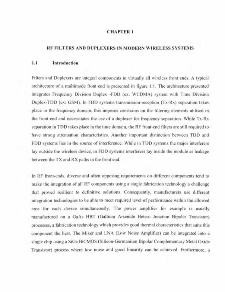
RF FILTERS AND DUPLEXERS IN MODERN WIRELESS SYSTEMS
1.1 Introductio n
Filters an d Duplexer s ar e integral component s i n virtually al l wireles s fron t ends . A typical
architecture o f a multimode fron t en d i s presented i n figur e 1.1 . The architectur e presente d
integrates Frequenc y Divisio n Duple x -FD D (ex : WCDMA ) syste m wit h Tim e Divisio n
Duplex-TDD (ex : GSM) . I n FD D system s transmission-receptio n (Tx-Rx ) separatio n take s
place i n th e frequenc y domain , thi s impose s constrain s o n the filtering elements ufilise d i n
the front-en d an d necessitate s th e use of a duplexer fo r frequenc y separation . Whil e Tx-Rx
separation in TDD takes place in the time domain, the RF front-end filters are still required to
have stron g attenuatio n characteristics . Anothe r importan t distinctio n betwee n TD D an d
FDD systems lie s in the source of interference . Whil e in TDD systems the major interferer s
lay outside the wireless device , in FDD systems interferers la y inside the module as leakage
between the TX and RX paths in the front end .
In RF front-ends , divers e an d often opposin g requirements o n differen t component s ten d t o
make the integration o f all RF components using a single fabrication technolog y a challenge
that prove d resilien t t o definitiv e solutions . Consequently , manufacturer s us e differen t
integration technologie s to be able to meet required leve l of performance withi n the allowed
area fo r eac h devic e simultaneously . Th e powe r amplifie r fo r exampl e i s usuall y
manufactured o n a GaA s HB T (Galliu m Arsenid e Heter o Junctio n Bipola r Transistor )
processes, a fabrication technolog y which provides good thermal characteristics that suits this
component th e best . Th e Mixe r an d LN A (Lo w Nois e Amplifier ) ca n b e integrate d int o a
single chip using a SiGe BiCMOS (Silicon-Germanium Bipola r Complementary Metal Oxide
Transistor) proces s wher e lo w nois e an d goo d linearit y ca n b e achieved . Furthermore , a

16
significant effor t ha s bee n pu t t o integrat e thes e module s i n a syste m o n packag e styl e
providing excellent performance an d miniaturization.
Unfortunately, antennas , filters and duplexer s hav e largel y eluded thes e miniaturizatio n an d
integration trends . Filters an d duplexer s ar e high Q-facto r passive s o f relatively larg e size -
measured i n term s o f th e guide d wavelength - the y ar e mostl y extema l component s t o th e
other integrated circuit s in the front-end .
Different solution s have been proposed fo r the design of miniaturized high-Q passives for RF
fronts ends . Th e mos t popula r o f whic h i s usin g acousti c wav e technologies , thes e hav e
found suppor t fro m equipmen t manufacturer s a s acousti c wav e filters quickl y becam e th e
industry de-fact o technolog y fo r miniaturize d filters. Therefore , SA W (Surfac e Acousti c
Wave) an d BA W (Bul k Acousfi c Wave ) ar e foun d i n ever y use r terminal . A majo r
disadvantage o f thes e filters i s tha t thei r fabricatio n proces s i s incompatibl e wit h thos e o f
other component s o f th e fron t end , als o lo w powe r handlin g capacity ; stabilit y an d a
relatively hig h insertio n los s ar e als o concems . Fabricatio n proces s incompatibilit y o f
acoustic wave devices stems from th e characteristics of their fabrication processes ; for SAW
filters, fragility an d the need of hermetic packaging inhibits their monolithic integration with
active component s [1] . On th e other hand BA W filters have mechanica l characteristic s tha t
are more integration friendly , bu t th e materials used and the fabrication constraint s required
for BA W fabricatio n ar e largel y differen t fro m th e standar d activ e device s fabricatio n
process such that monolithic integratio n result s in a more expensive, lower yielding process,
therefore, monolithic integration of BAW integration i s disadvantageous[l].

17
Antenn;i
L/ RF BP F
GSM1900
V L N A
p ^ Power Amplifie r
P-V L N A
V L N A
Power Amplifie r
P-VLNA
—I?-
LO
-ir-L O
SiG« B I C M O S |
GaAs HB T I
Figure 1.1 multi-mode front end module with emphasis on integration technologies.
Researchers have dedicated a lot of attention to planar filter and duplexer miniaturization in
recent years owing to their ease of fabrication, seamles s integration potential, power handling
capability, stability and cheap price.
This renewe d interes t fo r technologie s suc h a s MHMI C an d MMI C hav e produce d
significant advance s i n the design technique s o f miniature plana r filters. Plana r fabricatio n
processes hav e distinc t advantage s o n other processe s i n terms o f cost , integration , powe r
handling an d stability; moreover , thes e processes ar e mature and have prove n t o give high
yield in a high volume context. The major disadvantag e of these technologies is the inherent
difficulty o f designin g filtering stmcture s tha t accommodat e lo w GH z frequency circuit s
having low insertion loss , small fractional bandwidth (<5%), and miniaturized size.
In thi s wor k w e tackle the miniaturization proble m o f filters and duplexers targetin g thos e
fabrication technologie s o f active front-en d component s i.e . LNA and PA, these processe s
are fiindamentally planar i n nature o f which MHMI C an d MMIC processe s ar e examples.
Our techniqu e i s base d o n a topologica l optimizatio n o f folde d hal f wavelengt h couple d
resonators filter.
18
1.1.1 Plana r RF Filters
Planar R F filter s ar e these filters that us e plana r stmcture s t o realis e th e filtering elements.
These filters are typically manufactured a s MicroStrip (MS) or Coplanar Wave Guide (CPW)
stmctures, whether distributed o r lumped. Distributed planar filters tend to be relatively large
due t o th e us e o f resonator s whos e size s ar e comparabl e t o th e wavelength . A t lo w GH z
frequencies, th e are a occupie d b y thes e filters inhibit s thei r us e i n man y application s an d
eliminates th e optio n o f thei r monolithi c integratio n i n mode m use r termina l front-ends.
While lumpe d componen t filters d o no t suffe r fro m th e aforementione d drawback ; thei r
power handling capacity and Q factor a t high frequencies ten d to be poor.
RF filters use d i n mode m mult i mode/ban d fron t end s ar e predominantl y ban d pas s filters
with relatively low fractional bandwidth. To design such filters in planar stmctures ; coupled
resonators technique s ar e widel y employed . Recently , cros s couplin g technique s ar e
extensively utilise d t o inser t finite frequenc y transmissio n zero s fo r enhance d skir t
characteristics an d reducin g th e numbe r o f resonator s use d i n th e filter; consequentl y
reducing the filter size.
The system characteristics of filters that are of concem in the context of this current research
are insertion loss , retum loss , attenuation an d relative size . These characteristic s ar e define d
as follows:
- Insertio n Los s (IL) : I s the loss in signal powe r resulfing fro m th e insertion o f the
filter in the path of the signal. I t is expressed a s the ratio of the incident power Pi n
to its input port to the output power from its output port Pou t i n the pass band of the
filter. Thi s quantit y i s measure d i n term s o f th e transmissio n scatterin g networ k
parameters (S2 1 an d S12 ) commonl y use d i n vecto r networ k analyzers . Thes e
quantities are represented mathematicall y as:
IL=l01og(P,J-101og(P,,,) (1.1 )

19
It is generally required that the insertion loss be kept to a minimum especially in the context
of RF front-ends, where less than 3dB are typically accepted values.
- Retur n Los s (RL) : I s the power reflecte d fro m th e filter as a result o f impedanc e
mismatch betwee n th e sourc e and filter. I t i s expressed a s the ratio o f the inciden t
power Pi n t o it s inpu t por t t o th e reflecte d powe r fro m it s inpu t portP^ f . Thi s
quantity i s measure d i n term s o f th e adaptatio n scatterin g networ k parameter s
(Sll an d S22) commonl y use d i n vecto r networ k analyzer . Thes e quanfitie s ar e
represented mathematically as:
RL=101og(PiJ-101og(P,,,-) (1.2 )
- Attenuation : The attenuation i s a transmission characteristi c o f the filter; it can be
considered th e insertio n los s i n th e sto p ban d o f th e filter. I t i s measure d b y th e
same transmission scatterin g parameters as the insertion loss. In the context of multi
band/mode operafion i t is imperative to distinguish two distinct frequency bands.
o Narro w Ban d Attenuation : I t i s the attenuatio n characteristi c o f the filter
near th e pas s ban d o f th e filter. Thi s attenuatio n usuall y i s specifie d a s a
required attenuatio n leve l a t a finite frequenc y whic h in turn determines the
required steepness of the filter and consequently the order of the filter.
o Wid e Band Attenuation: I t is the attenuation characteristic s of the filter up
to an d beyon d th e secon d harmoni c o f th e centra l frequenc y o f th e filter.
This characteristi c i s very importan t du e t o the inheren t propert y o f plana r
resonant stmcture s t o hav e repeated an d spuriou s pas s bands harmonic s o f
the filter's centra l frequency . Specia l attention has to be given to assure that
the wide band attenuatio n characteristi c o f the filter does no t allo w signal s
from other modes/bands to interfere with signals of the operafional band .

20
Both o f thes e characteristic s ar e represente d b y th e transmissio n scatterin g networ k
parameters (S12 and S21).
- Relativ e Size: In the context of our research we will define the size of the filter
as th e minimu m rectangl e require d t o plac e th e filter o n a substrate . Th e
rectangle's widt h and breadth wil l be measured i n terms of the>ig. Where Xg is
defined a s the guided wavelength of a transmission line on the same substrate of
the filter. For example a filter may occupy a n area o f 60mmx20m m whil e the
guided wave length could be 11m m ; then the fdter size is 6A.gx2>tg.
1.1.2 Duplexer s
Duplexers ar e passiv e thre e por t device s tha t allo w a singl e antenn a t o b e share d
simultaneously b y a transmitte r an d a receive r operatin g i n clos e bu t separat e frequenc y
bands. Th e ports of a duplexer ar e transmission port , reception port , an d an antenna port a s
depicted in Figure 1.2 .
In th e contex t o f mode m multimod e FD D fron t ends , efficien t utilizatio n o f th e availabl e
bandwidth require s guard bands to be relatively small . Moreover , du e to the large dynamic
range between the transmitted signa l and the received one - typicall y more than 70 dB - i t is
required tha t th e duplexe r provid e stee p separatio n betwee n th e tw o band s fo r prope r
fiancfionality o f the system and efficient bandwidt h utilisation . I t is worth noting that in FDD
systems th e nois e i s intemall y generate d from th e system ; sinc e ther e ar e tw o differen t R F
signals propagating through the system.

21
Antenna
Matching Network
A/4
P2 T o Reciever
Figure 1. 2 Duplexer architecture.
Duplexers ar e made o f two band-pas s filters; on e connect s t o th e transmitte r an d th e other t o
the receiver , eac h o f thes e port s i s a port o f th e duplexer . Th e othe r tw o port s - one o f eac h
filter - ar e separate d b y quarte r wav e transmissio n lin e an d a matchin g networ k connectin g
the third outpu t por t o f the duplexer t o the antenna .
The syste m characteristic s o f duplexers o f conce m i n the contex t o f this curren t researc h ar e
insertion loss , retum los s an d isolatio n an d relativ e size . These characteristic s ar e defined a s
follows:
- Insertio n Los s (IL) : The insertio n los s o f th e duplexe r i s define d similarl y t o tha t
of the filter. Th e only difference i s that duplexers have two distinc t pas s bands; on e
for th e transmission , th e othe r fo r th e reception . Th e Insertio n los s fo r th e
transmission ban d i s commonl y require d t o b e abou t Id B les s tha n tha t o f th e
receiving band .
- Retur n Los s (RL) : The retum los s of the duplexer i s defined similarl y to that o f the
filter. Th e onl y differenc e i s tha t duplexer s hav e tw o distinc t pas s bands ; on e fo r
the transmission, th e other for th e reception .
- Relativ e Size : Defined similarl y to planar filters above .
9?
- Isolation : I t i s th e relativ e attenuatio n provide d betwee n th e tw o path s o f th e
duplexer; transmitte r t o antenn a pat h an d antenn a t o receive r path . A s w e indicate d
before thi s characteristi c i s of fundamenta l importanc e i n the syste m becaus e o f th e
large dynamic between th e transmitted signa l an d th e received one .
o T x i n R x band : I t i s th e attenuatio n provide d b y th e duplexe r fo r a signa l
having a frequenc y equivalen t t o tha t o f th e receptio n ban d whe n injecte d
from th e transmission por t of the duplexer .
o R x i n T x band : I t i s th e attenuatio n provide d b y th e duplexe r fo r a signa l
having a frequency equivalen t t o that o f the transmission ban d whe n injecte d
from th e reception por t o f the duplexer .
1.2 Surve y o f pertinent researc h activitie s
Miniaturization effort s followe d differen t approache s o n bot h th e fabricatio n an d th e desig n
front. Sinc e w e ar e primaril y conceme d wit h th e desig n aspect s o f miniaturization , w e wil l
present here the most pertinen t approache s followe d b y different researc h team s in this field.
A direc t approac h fo r achievin g highly miniaturized filters i s to use lumped components ; thi s
achieves miniatur e filters bu t suffer s ver y poor performanc e i n terms o f losse s an d steepnes s
of attenuation whe n standar d processe s ar e employed . Th e origin o f this poo r performanc e i s
mainly tha t th e qualit y facto r o f inductor s an d capacitor s deteriorate s rapidl y a t radi o
frequencies. Mode m MMI C proces s ca n achiev e hig h qualit y facto r (>500 ) fo r capacitors ,
but qualit y factor s fo r inductor s remain ver y limited whe n using finit e conductivit y metals . I n
[2] Hig h Temperatur e Superconductor s (HTS ) wer e use d t o realis e a 3' '' . orde r bandpas s
lumped element s filter, th e us e o f HT S materia l allowe d fo r th e realisatio n o f inductor s wit h
high qualit y factors . Whil e result s reporte d i n [2 ] ar e satisfactor y i n performanc e an d
miniaturization, th e filters us e uniqu e material s an d fabricatio n proces s tha t ar e no t directl y
23
compafible with commercially available MMIC process; moreover, the use of HTS requires a
cooling mechanism fo r materials to maintain their superconductive properties.
Another altemafiv e t o overcome inducto r losse s whe n designin g lumpe d component s filters
is to use Q-enhanced o r active inductors as suggested in [3]. This technique increases slightly
the are a o f inductor s use d i n th e desig n bu t allow s fo r arbitrar y Q-factor . Problem s o f
impedance matching between activ e and passive components, non linearity and stability tend
to limit the application o f these filters to IF frequency ranges. Furthermore, in the context of
RF front ends , powe r efficienc y i s a majo r conce m fo r batter y operate d use r terminals ;
consequently the use of active components is not suitable.
A differen t approac h fo r filter miniaturizatio n ha s bee n develope d aroun d hair-pi n filters.
Hairpin filters ar e classica l couple d resonato r filters. Th e s o calle d Hairpi n stmctur e i s
considered a folded for m of half-wavelength transmissio n line resonators.
In [4] the arms of Hairpin resonator were folded fo r the purpose of filter miniaturization an d
direct couplin g wa s used t o produce a third orde r miniatur e filter. Furthe r development s i n
[5] introduced stmctura l improvemen t to the hairpin resonator and cross coupling techniques
were introduced to provide a miniature and highly selective filter.
Finally, i n [6 ] the filter introduced i n [4 ] was realised usin g multilayer inte r coupling on an
LTCC (Low Temperature Co-fire d Ceramic ) process. This technique has produced excellen t
miniaturization result s fo r a fou r quasi-ellipti c ban d pas s filter, bu t losse s wher e relativel y
high fo r meta l thicknesse s accessibl e usin g thi s technology , als o som e divergence betwee n
the electromagneti c simulatio n an d th e measurement s obtaine d du e t o th e difficultie s o f
simulating th e mult i laye r inte r coupling . Despit e thes e problem s thi s techniqu e promise s
very high miniaturizatio n potentia l an d coul d prov e to be very successfril . I t is worth notin g
that thi s technique ca n be utilized t o further miniaturiz e th e filters we developed, providin g
additional miniaturization for our filters.

24
Moreover, anothe r approac h i s t o us e dua l mod e resonators . A dua l mod e resonato r i s a
resonator that i s designed to excite high order modes and recombine them a t the output port .
These modes have slightly different resonan t frequencies whic h allows for the design of band
pass filters. Th e miniaturizatio n aspec t stem s from th e fac t tha t onl y a singl e resonato r i s
required t o desig n a filter. Good miniaturizatio n ca n b e achieve d usin g thi s technique s bu t
due to the sensitivit y o f the excited mode s to the symmetry of the resonator, th e size of the
resonator remain s large r tha n mult i resonato r filters designed b y alternativ e techniques . An
example of a miniaturized filter of this type is a fractal dua l mode filter presented in [7].
Finally, anothe r approac h fo r filter miniaturizatio n i s t o find a miniatur e topolog y wit h
minimal Ohmic losses. In [8] a new methodology for topological compacting was introduced,
also a se t o f filters an d a duplexer fo r UMT S front en d wa s designe d an d fabricate d o n a
standard alumin a substrate . Th e filters an d th e duplexe r reporte d hav e achieve d hig h
performance an d compac t size . Thes e ar e th e mos t miniatur e filters t o ou r knowledg e i n
single layer Microstrip stmctures.
After w e have reviewed the different approache s in designing planar filters, we will present a
comparative table to compare the respective performance of each of these techniques.
Table 1. 1
A comparative table between the different approache s
Approach
Lumped Components (HTS)
Hairpin multilaye r
Dual Mode Resonators (Fractal)
Topological Optimizatio n
Fractional
Bandwidth
0.844%
3.7%
1%
2.5%
Attenuation
-60dB
-30dB
-50dB
-45dB
Size
10mmx3.5mm
5x7mm0.16X0.11
20mmx20mm 0.15X0.15
9mmx7.5mm 0.125X0.1 5
Central
Frequency
1.7GHz
3GHz
0.85GHz
2GHz
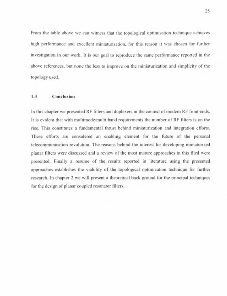
25
From th e tabl e abov e w e ca n witnes s tha t th e topologica l opfimisafio n techniqu e achieve s
high performanc e an d excellen t miniaturisation , fo r thi s reaso n i t wa s chose n fo r furthe r
investigation i n our work . I t i s our goa l t o reproduce th e sam e performance reporte d i n the
above references , bu t non e th e les s to improv e o n the miniaturization an d simplicit y o f th e
topology used.
1.3 Conclusio n
In this chapter we presented R F filters and duplexers in the context of modem RF front-ends .
It is evident tha t with multimode/multi band requirements the number of RF filters is on the
rise. Thi s constitute s a fundamenta l thms t behin d miniaturizatio n an d integratio n efforts .
These effort s ar e considere d a n enablin g elemen t fo r th e futur e o f th e persona l
telecommunication revolution . Th e reasons behin d th e interes t fo r developin g miniaturize d
planar filters were discussed an d a review o f the most mature approaches i n this filed were
presented. Finall y a resum e o f th e result s reporte d i n literatur e usin g th e presente d
approaches establishe s th e viabilit y o f th e topologica l optimizatio n techniqu e fo r furthe r
research. I n chapter 2 we will present a theoretical back groun d fo r the principal technique s
for the design of planar coupled resonator filters.
CHAPTER 2
PRINCIPLES OF COUPLED RESONATORS FILTE R DESIGN
2.1 Introductio n
In thi s chapte r w e ar e conceme d wit h buildin g a knowledge bas e o f th e som e o f the mos t
fundamental an d widely used concept s i n coupled resonator s filter design. We start with the
general theor y o f direc t couple d resonato r filters an d thei r synthesi s fro m lo w pas s
prototypes, the n we wil l us e general filter theory o f lumped elemen t technique s t o illustrat e
the concept of transmission zero s at finite frequencies. Subsequently, we will explain how in
direct couple d resonato r topologie s ar e use d t o realis e transmissio n zero s a t finit e
frequencies.
2.2 Desig n of direct coupled resonator band pass filters
Direct couple d resonato r filters i n thei r mos t elementar y for m coul d b e represente d a s i n
Figure 2. 1 below . Al l resonator s ar e identica l an d ar e directl y couple d t o on e anothe r a s
depicted in the figure. Th e value of the coupling coefficient i s denoted byA/„ „^| an d can be
positive or negative. Coupling between non adjacent resonator s is neglected. The coupling to
the extemal port s i s denoted b y the extemal qualit y factor^g . Coh n i n [9 ] has introduce d a
method fo r designin g couple d resonator s bandpas s filters from lowpas s prototypes . Late r i n
[10] he applied hi s method t o design a multitude o f different stri p line parallel transmissio n
line resonators. The metho d i s based o n a theoretical derivatio n o f a n equivalen t circui t fo r
microwave couple d resonator s suc h tha t th e couplin g betwee n resonator s act s a s a n idea l
immittance inverter .

27
Q e M,, 2 n/ \ M3.4
Rin: H H
1] Ht-n Hl-i r"! H h H H HHi
M,
-Direct Couplin g
Figure 2.1 A general representation of direct coupled resonators filter.
The goa l o f Cohn' s metho d i s t o establis h a relatio n betwee n th e circui t parameter s o f a
prototype filter an d th e couplin g parameter s o f th e microwav e resonator s arrangement , i.e. ,
the couplin g coefficientsM „ „^] , an d th e extema l qualit y factor^^ . Disha l i n [11 ] ha s
described a n experimenta l metho d fo r findin g th e couplin g coefficien t an d th e extema l
quality facto r o f couple d resonators . Thi s metho d ca n b e adapte d t o wor k i n th e contex t o f
modem electromagneti c simulatio n technique s instea d o f measurements . Therefore , usin g
the combination o f Cohn's formulatio n an d DishaFs technique we can design bandpass filters
from lowpas s prototypes wit h relatively littl e effort .
It i s important befor e furthe r detai l t o mention tha t ther e ar e different qualit y factor s tha t ca n
be associate d wit h circuit . Hence , i t i s important t o discuss the m an d t o identify th e qualifie s
they measure a s well a s the relation between them .
A qualit y facto r i s a ratio betwee n energ y storag e an d energ y los s i n a resonator. Dependin g
on the origin o f the losses being considered on e can define thre e quality factors [12] :
Unloaded Q : Q,=( o _ Energ y stored i n theresonant circui t
Extemal Q : QE= M
Power los s in the resonant circui t
Energy stored i n the resonant circui t Power los s in the extemal circui t
(2.1)
(2.2)
28
Loaded Q: Q , =o) Energy stored in the resonant ircuit Total power loss
These three factors are related by the following equation :
_L-_L J _
(2.3)
(2.4)
In the planar filter design contex t we are more concemed with the extemal qualit y facto r Qe,
as the unloaded qualit y facto r Qu has an upper limit that can not be surpassed fo r a particular
fabrication technology . Also , it is very common that the values of Qe required fo r realizing a
filter is much lower than that of Qu; and consequently becomes more dominant.
In thi s sectio n w e wil l explai n i n som e detai l ho w t o deriv e th e equivalen t circui t a s pe r
Cohn's method . The n w e wil l illustrat e ho w DishaF s metho d wa s adopte d t o calculat e th e
coupling coefficients usin g electromagnetic simulation .
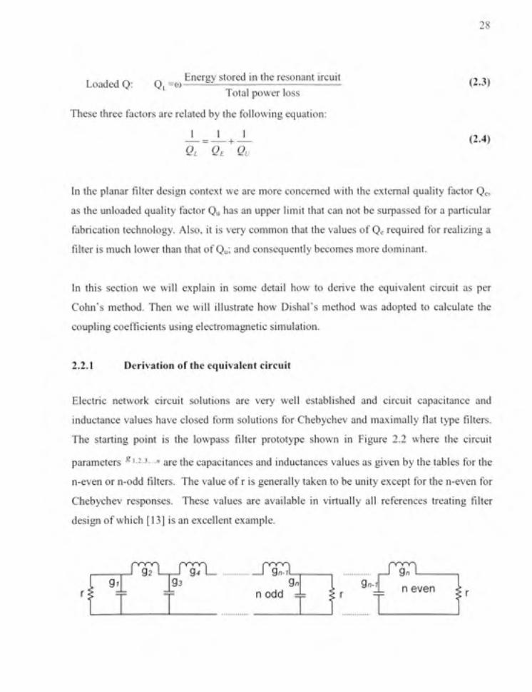
2.2.1 Derivation of the equivalent circuit
Electric networ k circui t solution s ar e ver y wel l establishe d an d circui t capacitanc e an d
inductance values have closed for m solution s fo r Chebychev and maximally flat type filters.
The startin g poin t i s th e lowpas s filter prototyp e show n i n Figur e 2. 2 wher e th e circui t
parameters ^'^.s , , « j-g t^g capacitances and inductances values as given by the tables for the
n-even or n-odd filters. Th e value of r is generally taken to be unity except for the n-even fo r
Chebychev responses . Thes e value s ar e availabl e i n virtuall y al l reference s treatin g filter
design of which [13] is an excellent example.
g?_ J171 J 9 4 L _ 1 Qn-r l
93 JXl
9n-7 ^ _ L n even

29
Figure 2.2 Low pass prototype filter of Chebychev or maximally flat response.
To transfor m th e lowpas s prototyp e t o a bandpas s filter w e us e th e lowpas s t o highpas s
transformation show n in Figure 2.3.
LP to BP Transformation R_
6
Sc
gL
A is the fractiona l bandwidt h o f the filte r
(Ofj i s the central frequenc y o f the filter
(^OSL
SL a)„A
Figure 2.3 Lowpass to Highpass Filter Transformation.
Applying thi s transformatio n t o th e lowpas s prototyp e yield s a bandpas s filter wit h th e
corresponding bandwidth , centra l frequency , an d attenuatio n characteristic s a s illustrated i n
Figure 2.4

Bandpass filter trasnformed from lowpas s prototype
30
rem rrm rem
]i > ' L , =
rrm
^ L „
Figure 2.4 Trasnformed bandpass filter (Bottom) Circuit transformation.
In order t o transform th e band pas s filter to a form tha t approximate s tha t o f figur e 2.1 , we
need t o get rid of the parallel arm s of the filter. Consequently, th e next ste p i s to transfor m
the bandpass filter to an equivalent circui t with only series or parallel resonator section s and
immittance transformers . Immittanc e transformer s allo w th e transformatio n o f a serie s
section to a parallel section and vice versa [7].
Impedance inverters Admittanc e inverters
57 K
±90° 0 T
''I
J
±90°
i
1 r.-y-
Figure 2.5 Conceptual operation of immittance inverters.
The conceptua l operatio n o f immittanc e transformers , als o calle d inverters , i s illustrate d i n
Figure 2.5. I t was demonstrated by Dishal in [11] that these immittance transformers ca n be
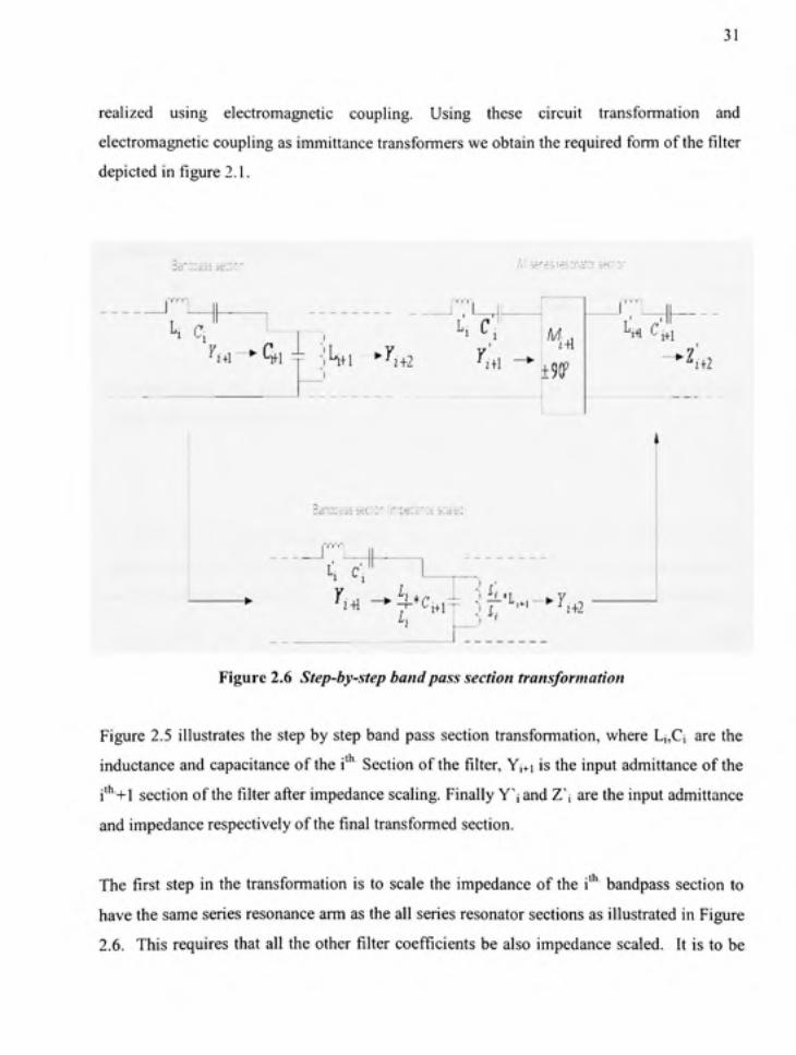
31
realized usin g electromagneti c coupling . Usin g thes e circui t transformatio n an d
electromagnetic couplin g a s immittance transformer s w e obtain the required for m o f the filter
depicted i n figure 2.1.
3H'::iiiiiii"C~ Ai:5=-'53re$*n3!"r5efy
kc, y^ +1 ^tfl
. ^ i :L, '1+1 -y, J+2 •1+1
H4 +90P
J " ^41 C m tj+ j
'1+2
ianSDrij sec:D' inDe:£"t Ka-c.
J'"'"'
i+i Vc 1+1 "i • ^ i . T Y
1+2
Figure 2.6 Step-by-step band pass section transformation
Figure 2. 5 illustrate s th e ste p b y ste p ban d pas s sectio n transformation , wher e Li,C i ar e th e
inductance an d capacitanc e o f th e i ' Secfio n o f the filter , Yj+ i i s the inpu t admittanc e o f th e
i" -i-l sectio n o f the filter afte r impedanc e scaling . Finall y Y"i and Z' j ar e the input admittanc e
and impedanc e respectively of the final transformed section .
The first ste p i n th e transformatio n i s t o scal e th e impedanc e o f th e i" ^ bandpas s sectio n t o
have the same serie s resonance ar m a s the al l serie s resonator section s a s illustrated i n Figur e
2.6. Thi s require s tha t al l th e othe r filter coefficient s b e als o impedanc e scaled . I t i s t o b e
32
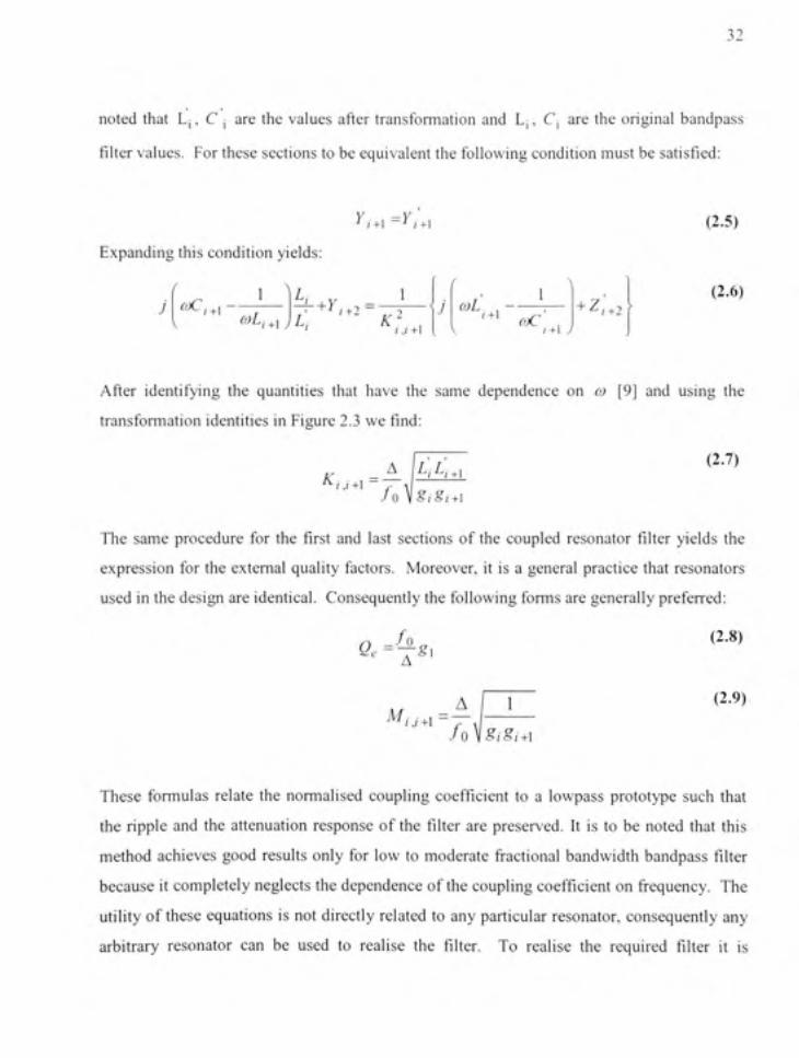
noted tha t Lj , C j ar e th e value s afte r transformatio n an d L; , C j ar e th e origina l bandpas s
filter values . Fo r these sections to be equivalent th e following conditio n mus t b e safisfied :
^i+\ - ^ j + i
Expanding thi s condition yields :
<^i+i - 0)1 L
i +1 J Li ^+y..2=—.
K I 4 + 1
(oL i+\ o)C
+ '^,^2 i+\ J
(2.5)
(2.6)
After identifyin g th e quantitie s tha t hav e th e sam e dependenc e o n co [9 ] an d usin g th e
transformation identitie s i n Figure 2.3 we find:
K i ,i +1 A L,L„, (2.7)
fQ\S,gi+\
The sam e procedur e fo r th e first an d las t section s o f th e couple d resonato r filter yield s th e
expression fo r th e extema l qualit y factors . Moreover , i t i s a genera l practic e tha t resonator s
used i n the design ar e identical. Consequentl y the following form s ar e generally preferred :
a. -i^..
^ , - , /+ l= —
(2.8)
(2.9)
/o V / <+l
These formula s relat e th e normalise d couplin g coefficien t t o a lowpas s prototyp e suc h tha t
the ripple an d th e attenuatio n respons e o f th e filter ar e preserved . I t i s t o b e note d tha t thi s
method achieve s goo d result s onl y fo r lo w t o moderat e fractional bandwidt h bandpas s filter
because i t completely neglect s th e dependence o f the coupling coefficien t o n frequency . Th e
utility o f thes e equation s i s no t directl y relate d t o an y particula r resonator , consequentl y an y
arbitrary resonato r ca n b e use d t o realis e th e filter. T o realis e th e require d filter i t i s

33
necessary t o b e abl e t o achiev e th e couplin g coefficient s value s require d b y th e equation s
above. Th e couplin g i s mainl y dependan t o n geometrica l parameter s an d i s determine d b y
either experiment and/o r electromagneti c simulatio n a s explained i n the following section .
2.2.2 Extractio n o f coupling coefficients usin g electromagnetic simulatio n
The couplin g coefficient s betwee n resonator s M, ,+, , th e extema l qualit y factor^,, , an d th e
unloaded qualit y facto r ^ „ ar e the only parameters a designer i s required t o know i n order t o
realise a bandpass couple d resonato r filter a s w e hav e previousl y illustrated . Onc e th e basi c
resonator i s chosen , th e unloade d qualit y facto r ^ „ i s fixed an d i s mainl y controlle d b y th e
fabrication technolog y parameter s suc h as ; meta l conductivity , substrat e los s tangent , an d
metal thickness . Consequently , th e desig n parameter s o f interes t ar e Q^ and th e couplin g
coefficients M , , + i . I n [11 ] a detaile d method , referre d t o a s DishaF s procedure , fo r
measuring thes e parameter s i s presented . I n thi s sectio n w e ar e conceme d wit h th e
application o f this method usin g ADS/Momentum electromagneti c simulatio n [14] .
The setu p fo r measurin g th e couplin g coefficient s betwee n tw o half-wavelengt h Microstri p
resonators i s shown i n Figure 2.7 . Th e method call s fo r detectin g th e amplitud e respons e t o
an excitatio n fro m a source that lightl y load s the resonato r (i.e . decrease the unloaded qualit y
factor b y les s tha n 10%) . Fro m th e amplitud e respons e th e couplin g coefficien t an d th e
extemal qualit y facto r ar e calculate d b y recordin g th e peaks , th e frequency differenc e
between thes e peaks , an d th e fractiona l bandwidt h o f th e response . Consequently , fo r
different value s o f th e geometrica l parameter s X an d 5 on e ca n calculat e bot h coefficient s
for an y desired configuration . W e wil l carr y ou t thi s procedure vi a ADS\Momentu m usin g a
co-simulation technique . Th e co-simulatio n techniqu e permit s th e simulatio n o f circui t
elements, lumpe d o r distributed , an d distribute d layou t component s simultaneously . Th e
layout component s ar e simulate d vi a electromagneti c simulatio n an d th e circuit s ar e

34
simulated base d o n thei r respectiv e circui t models . Usin g thi s techniqu e a parameterize d
layout o f th e couple d resonator s wa s buil t an d ver y lo w lumpe d capacitor s wer e use d t o
lightly couple the ports of the resonators.
Matched Sourc e
Lightly Couple d
Source
Coupled Resonators
Detector
Lightly Couple d
X \ ^ Lightly Couple d Detector
Figure 2.7 (Left) Setup for Q^ measurement (Rigth) Setup for K measurement
2.2.2.1 Extractin g of coupling factor M
The circui t i n Figur e 2. 8 i s use d t o calculat e th e couplin g coefficien t M between th e
resonators for different value s of the distance X betwee n them.

35
III-7 —vw Term I Hum=1 Z=50 O h m
C 1 0=0 0 5 p F
^^ SP1
S-PARAMETERS
Stdrt=1 5 OH z Stop Step
=2 4 CH z = 750 kH z
1 E ]
/.= 1 0
K_Ctc-ff_1 X = X u m Mo del Type
^% PARAMETER SWEE P 1
i .K rep l S'AieepVdf="X" SirnlnstanceN3rne(1]="SPr' ?imlnstariceNarTie{21= Simlni1anc€N3me[JI= SirrilnstariceH3rTie[4]= 91 fTi! n t a n ce H J m e [5]= SirTilri<1flnceHjrTi«[61= Stjrt=500 Stop=2000 Step=
= MW
C=0 05 p F
AAA^7H|I
Num=2 Z=£0 O h m
Figure 2.8 Circuit co-simulation for determining coupling coefficient.
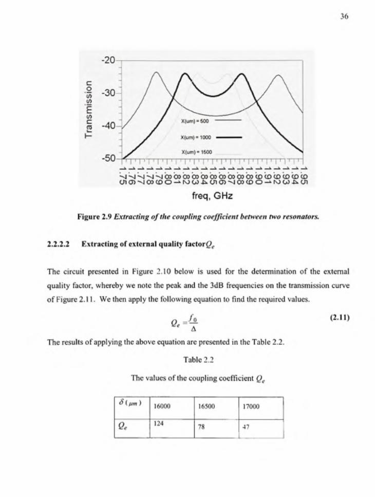
The results o f the simulation ar e presented i n Figure 2.9 below. B y inspection w e can find
that the central frequenc y /gi s 1.85GHz . Als o we can note the frequencies of the peaks on
the response for different value s of X an d we designate /;, to the higher frequency an d // t o
the lower frequency o f the response's peaks. Th e coupling coefficient ca n then be calculated
as follows:
M = fh ~fl /o
The following table summarises the results for the different value s of X.
Table 2.1
The values of the coupling coefficient M
Separation A' (/jm )
Coupling
Coefficient M
500
0.0784
1000
0.0346
1500
0.0162
(2.10)
36
c o </> "E (/) c .
I -
-20
X(um) = 500
X(um)=1000
X(um)=1600
I ' I ' I ' I ' M 1 ' I ' I I 1 ' i ' 1 ^
•^•vJ-vJ-^-vJC»O0O0O0O0O0O0O0O0C»CDCDCD(DCDCD c n a ) - - j o o ( D O - ^ K ) c o . ^ c n c D - ^ o o ( D O - » - N J C O - u c n
freq, GHz
Figure 2.9 Extracting of the coupling coefficient between two resonators.
2.2.2.2 Extractin g of external quality factor^^
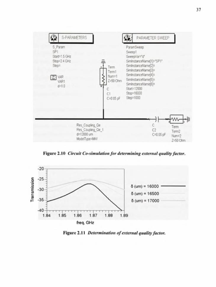
The circui t presente d i n Figur e 2.1 0 belo w i s use d fo r th e determinatio n o f th e extema l
quality factor , whereb y we note the peak and the 3dB frequencies o n the transmission curv e
of Figure 2.11. W e then apply the following equation to find the required values.
Qe = / o
The results of applying the above equation are presented in the Table 2.2.
Table 2.2
The values of the couplin g coefficient Q^
S (^m)
Qe
16000
124
16500
78
17000
47
(2.11)
37
© S-PARAMETERS 1
S Parar n SPl Start=1.5GHz Stop=2 4 GHz Step=
/AR VAR1 d=10
^% PARAMETER SWEE P
ParamSweep Sweep 1 SweepVar="ij" SimlnstariceName[1]="SPl"
jg^^ SimlristanceHame[2] = -[-pi-PPl SimlnstanceName[3] = Mum=1 SimlnstanceMame[4] = Z=50 Ohm SimlnstanceName[5] =
SimlnstariceName[6]= C Start = 12000 CI Stop= l C-0 05pF Step= l
Res_Coupling_Qe Res_Coupling_Qe_l cl=12000um ModelType=MW
1 - j ^ ^ Ter m ^2 Term 2 C=0 05pF ^j,m= 2
Z=50 Ohm
Figure 2.1 0 Circuit Co-simulation for determining external quality factor.
-20-
c o l/> </) F (/) c (0 1-
•25^
- 3 0 ^
•3fa-
-40 1 — I — I — I — I — I — I — I — I — I — I — I — I — I — I — I — I — I — I — I — I — I — r
1.84 1.8 5 1.8 6 1.8 7 1.8 8 1.8 9
5 (urn) = 16000
5(um) = 16500
5 (urn) = 17000
freq, GH z
Figure 2.1 1 Determination of external quality factor.
38
2.2.3 Transmissio n zero s at finite frequencie s
Direct couple d resonator s filter s ar e ver y versatil e an d relativel y simpl e t o design . Despit e
their attractiv e features , thes e filters ca n onl y realis e Chebyche v pas s ban d characteristics .
When these filters are used a t relatively low frequencies an d high selectivit y i s required, the
size an d losse s ten d t o b e ver y prohibitive . A wa y t o realis e highl y selectiv e filters i s t o
design filters tha t achiev e transmissio n zero s a t finite frequencies . Thes e filters have hig h
selectivity wit h lowe r filte r order , an d constitut e a ver y interestin g altemativ e fo r hig h
performance band pass filters.
A transmissio n zer o occur s i s whe n n o transfe r o f powe r betwee n th e sourc e an d th e loa d
takes place . Chebyche v ban d pas s filters, whether the y ar e based o n lumped o r distributed
components, achieve their zeros at infinite an d zero frequency. I n Figure 2.12 a Chebychev
band pas s filter circuit i s represented a t infinite frequenc y an d a t zero frequency . Fro m th e
figure w e ca n not e tha t th e C2 , LI , an d L 3 provide a transmission zer o a t zero frequency ,
while CI, L2 , and L4 provide a transmission zero at infinite frequency . Also , we note that a
3"* orde r Chebyche v filter wil l provid e a n equa l numbe r o f zero s a t zer o an d infinit e
frequencies.
Elliptic filters , o n th e othe r hand , ar e a famil y o f filters tha t achiev e transmissio n zer o a t
finite frequencies , givin g the m thei r superio r attenuatio n characteristics . Ellipti c filters are
similar t o Chebyche v filters i n tha t the y ar e equirippl e i n th e pas s band , bu t the y ar e als o
equiripple i n th e sto p band . A compariso n betwee n th e amplitud e respons e o f 3' ' * order
ellipfic and Chebychev filters is presented in figure 2.13.
Elliptic filters hav e bette r attenuatio n characteristic s becaus e o f th e existenc e o f finit e
frequency transmissio n zero s in their response. Unfortunately , transmissio n zeros come with
the pric e o f no n linea r phas e respons e whic h i s quit e importan t i n th e contex t o f
telecommunication terminals . Phas e equalisatio n ca n b e achieve d usin g phas e equalisatio n

39
sections a t the cos t o f large r filters. Altematively , quasi-ellipti c filters can approac h linea r
phase b y placin g transmissio n zero s a t imaginar y frequencie s [15] . I n the nex t sectio n w e
will present how to practically linearize the phase response of coupled resonator filters using
this approach. 3'". Order Chebychev
Filter
o PI Num=1
LI L=78 677748 pH R=le-12 0h m
R = 1e-12 0hm C=45 809417fF
C1 C=84 688009 pF
L3 L=78 677748 pH R = le-120hm
< 3 P2 Num=2
C3 C=84 68801 pF
Circuit at DC
o o
o o
-S C— O C
b o o
i 1 P2 Num=2
Circuit at infinite Freq.
o PI Num=1
o b
CO
b
OC — S C -
o b
CO
b
J P2 Num=2
Figure 2.12 3rd Order Chebychev filter at different frequencies.

40
-0
—10
-20
—30
-40
-50 1.70 1.75 1.80 1.85 1.90 1.95 2.00 2.0 5 2.10 2.15 2.20
freq, GHz
O CD CT
O 17 CD <
Figure 2.13 Amplitude response comparison between Chebychev and elliptic filters.
The circuit realisations of elliptic filters are more complex than those of the Chebychev. Fo r
the thir d orde r filter whos e amplitud e respons e i s show n i n figur e 2.13 , the correspondin g
circuit diagra m i s shown in figure 2.14 . W e can see from these figures that, similarly to the
Chebychev filter, LI an d L 4 provide a transmission zer o a t zero frequency, and that CI an d
C4 provide a transmission zer o at infinite frequency. Bu t unlike its Chebychev counter part ,
we find tha t th e tw o paralle l resonator s provid e tw o transmissio n zero s eac h a t a differen t
finite frequency. A summary of all the circuit elements providing transmission zero s at finite
and infinit e frequency i s provided i n Figur e 2.15 . Th e parallel combinatio n o f an inducto r
and capacitor wil l provide a transmission zer o corresponding t o an open circui t in the signal
path whe n inserte d i n serie s wit h respec t t o th e othe r resonators . B y analogy , th e serie s
combination of an inductor and a capacitor will provide a transmission zero corresponding to
a short circuit in the signal path when inserted in parallel to the other resonators.

3' . Orde r elliptic filter
41
O pi Num=l
L2 1=300.76057 pH R=1e-I2 0hrn
L1 1=67.572529 pH R=le-12 0hm
C1 C=98 606075 pF
L3 L=280.099526 pH R=1e-12 0hrn
1041 p F
L4 1=67.572529 pH R=le-12 0hm
• o P2 Num=2
C4 C=98 606075 pF
• ^
P1 Num=1
\ L I -' 1=67.57252 9 pH
R=1e-I2 0hm
1 M 1 0 c 1
@F=1.87GHz @ : : C I
C=98.606075 pF
o.c. 1 F=2.03GHz
J L 4 -P 1=67.57252 9 pH 1 R=le-1 2 0hm
- C 4 C=98.6060
• o P2 Num=2
rd Figure 2.14 Circuit diagram for i'^ order elliptic filter.
As we have seen in this section, transmission zeros have a profound effec t o n the attenuation
characteristics of a filters when they are achieved at finite frequencies . Filter s that have finit e
frequency transmissio n zero s ca n have ver y stee p attenuatio n wit h relativel y lo w order,
making the m a very attractiv e altemativ e whe n miniaturise d filters ar e required. Couple d
resonators filters can achieve finit e frequenc y transmissio n zeros , if non adjacen t resonator s
are allowed to be electromagnetically coupled . A more detailed study is presented in the next
section.
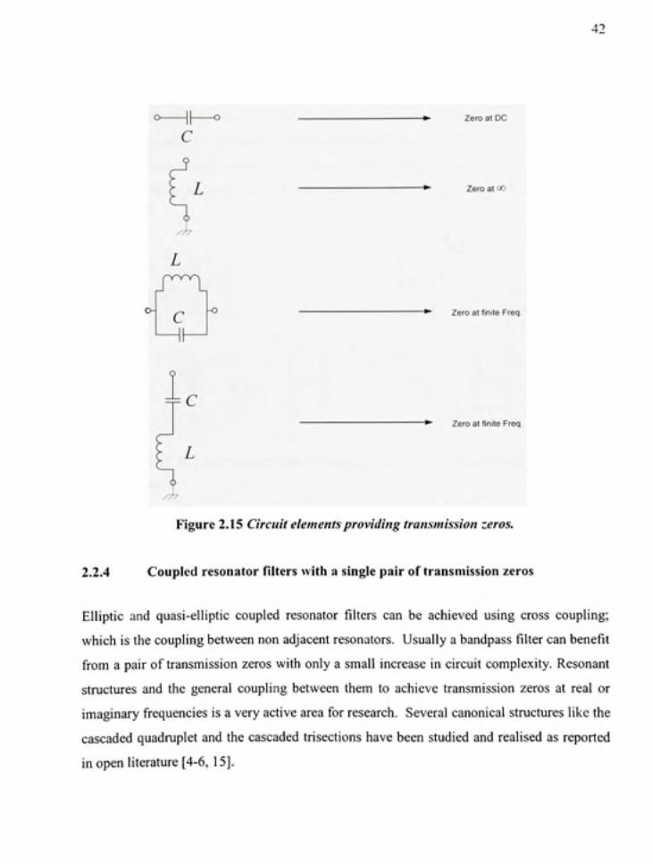
42
c
o- c -o
Zero a t DC
Zero at co
Zero at f nite Freq .
Zero at finite Freq .
O
1
L
Figure 2.15 Circuit elements providing transmission zeros.
1.1.4 Coupled resonator filters with a single pair of transmission zeros
Elliptic an d quasi-ellipti c couple d resonato r filters ca n b e achieve d usin g cros s coupling ;
which is the coupling between non adjacent resonators . Usuall y a bandpass filter can benefi t
from a pair of transmission zero s with only a small increas e i n circuit complexity . Resonan t
stmctures an d th e genera l couplin g betwee n the m t o achiev e transmissio n zero s a t rea l o r
imaginary frequencies i s a very active area for research. Severa l canonical stmctures like the
cascaded quadmple t an d the cascaded trisection s hav e been studie d an d realised a s reported
in open literature [4-6, 15].
43
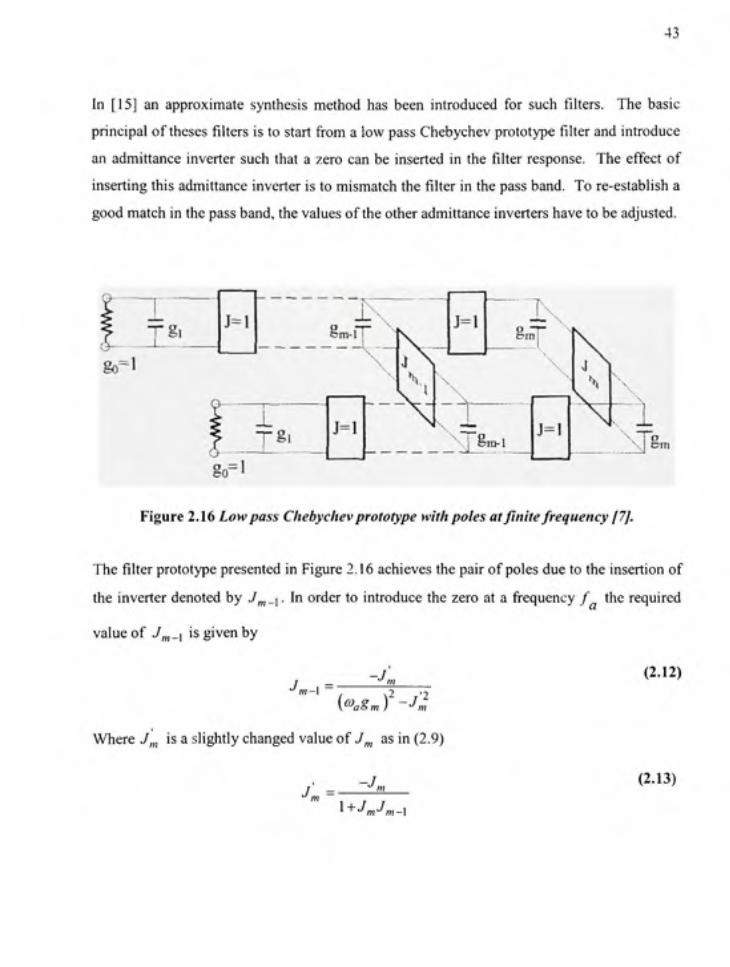
In [15 ] a n approximat e synthesi s metho d ha s bee n introduce d fo r suc h filters. Th e basi c
principal of theses filters i s to start from a low pass Chebychev prototype filter and introduce
an admittance inverte r suc h tha t a zero can be inserted i n the filter response. Th e effec t o f
inserting this admittance inverter is to mismatch the filter in the pass band. T o re-establish a
good match in the pass band, the values of the other admittance inverters have to be adjusted .
T g i
go= l
J-1
T 8 i
go=l
8m-fT
J-1
J=l
om-l J=1
_\J cm
Figure 2.16 Lowpass Chebychev prototype with poles at finite frequency [7].
The filter prototype presented in Figure 2.16 achieves the pair of poles due to the insertion of
the inverter denoted b y J^_i . I n order to introduce the zero a t a frequency / th e required
value of Jm-\ i s given by
Jm-\ -' -J„ (2.12)
•2 m
Where J,„ i s a slightly changed value of J^ a s in (2.9)
Jm = -J. (2.13)
1 + J ^ j ^ _ i
44
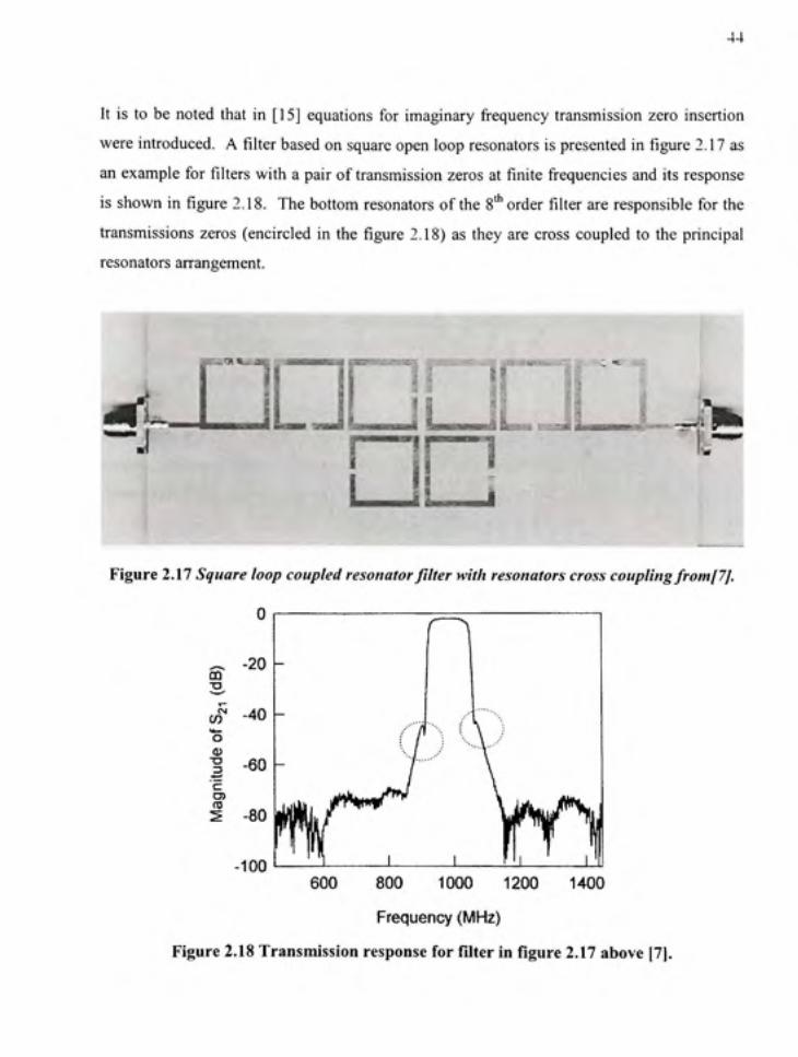
It i s t o be note d tha t i n [15 ] equation s fo r imaginar y frequency transmission zer o insertio n
were introduced. A filter based on square open loop resonators is presented in figure 2.1 7 as
an example for filters with a pair of transmission zero s a t finite frequencies an d it s response
is shown in figure 2.18. Th e bottom resonator s o f the S" ' order filter are responsible fo r the
transmissions zero s (encircle d i n the figure 2.18) a s they ar e cross couple d t o the principa l
resonators arrangement .
Figure 2.17 Square loop coupled resonator filter with resonators cross coupling from f7J.
0
^ _ CO T3 '-.^ T *
CO « -o 0) •o 3 C O) (0
-20
-40
-60
-80
-100
600 80 0 100 0 120 0 140 0
Frequency (MHz)
Figure 2.18 Transmission response for filter in figure 2.17 above [7] .

45
The coupling arrangement presented in figure 2.17 is used to introduce transmission zeros at
finite rea l frequencies . Thi s ha s th e effec t o f enhancin g th e attenuatio n o f th e filter.
Altematively, i f i t were require d t o lineariz e th e phase response o f the filter, i t would hav e
been possibl e t o d o s o by insertin g thes e zero s a t finit e imaginar y frequencies . A straigh t
forward techniqu e t o achiev e thi s i s by changing the typ e o f coupling o f the cros s couple d
resonators. Mor e precisely, the general coupling scheme in figure 2.1 7 is inductive coupling
and if capacitive coupling were used to couple the bottom resonators, then transmission zeros
would to be inserted at imaginary frequencies and a linearized phase response is achieved.
2.3 Conclusio n
In thi s chapte r w e hav e presente d som e o f th e mos t commo n technique s fo r designin g
coupled resonato r filters. W e hav e als o detaile d on e o f th e mor e advance d technique s i n
filter design , i.e . introductio n o f transmissio n zero s a t finit e frequencies . Th e insertio n o f
transmission zero s constitute s a fundamenta l techniqu e o n whic h ou r wor k i s based .
However, i t i s t o b e note d tha t i n ou r wor k w e us e geometrica l optimizatio n fo r filter
miniaturisation. I f we wer e t o us e the cros s couplin g techniqu e a s i n traditiona l method , i t
would have been necessary to re-extract th e coupling coefficients an d extemal qualit y facto r
for the resonators each time the geometry is changed.

CHAPTER 3
FILTERS AND DUPLEXERS I N MHMIC TECHNOLOGY
3.1 Introductio n
In this chapter we present th e design methodology adopte d i n this work in greater detai l and
its applicafio n t o realis e fihers o n MHMI C substrates . Firs t w e introduc e th e Xl4±5
resonator whic h i s the basic resonato r i n ou r work . Subsequently , w e use th e resonato r t o
design a second order filter. Two filter stmctures will be presented: the symmetrical feed and
the asymmetrica l fee d stmctures . Eac h o f thes e stmcture s exhibit s differen t transmissio n
zero location . Afte r evaluatin g the two stmctures , a candidate stmctur e wil l be selected fo r
miniaturisation. Filte r miniaturisatio n i s achieved vi a a geometrical optimizatio n techniqu e
which wil l b e thoroughl y studied . Finally , w e wil l presen t th e measurement s o f filters
fabricated o n MHMIC substrates.
To illustrate our design technique we will use both circuit and electromagnetic simulations to
study the response of different filter stmctures . W e begin wit h a single resonator, followe d
by a simple two resonator filter, and finall y w e present th e miniaturization techniqu e an d its
application t o th e filter stmcture . I n eac h ste p w e wil l stud y th e effec t o f relevan t
geometrical desig n parameters suc h a s the spacing between resonator s an d the displacemen t
of the fee d point . I n genera l terms , the optimality criteri a fo r th e geometrica l optimisatio n
technique use d wil l b e th e siz e o f th e filter an d it s performance . I n othe r words , th e
minimum filter size that fulfills th e performance requirements will be considered optimum.
47
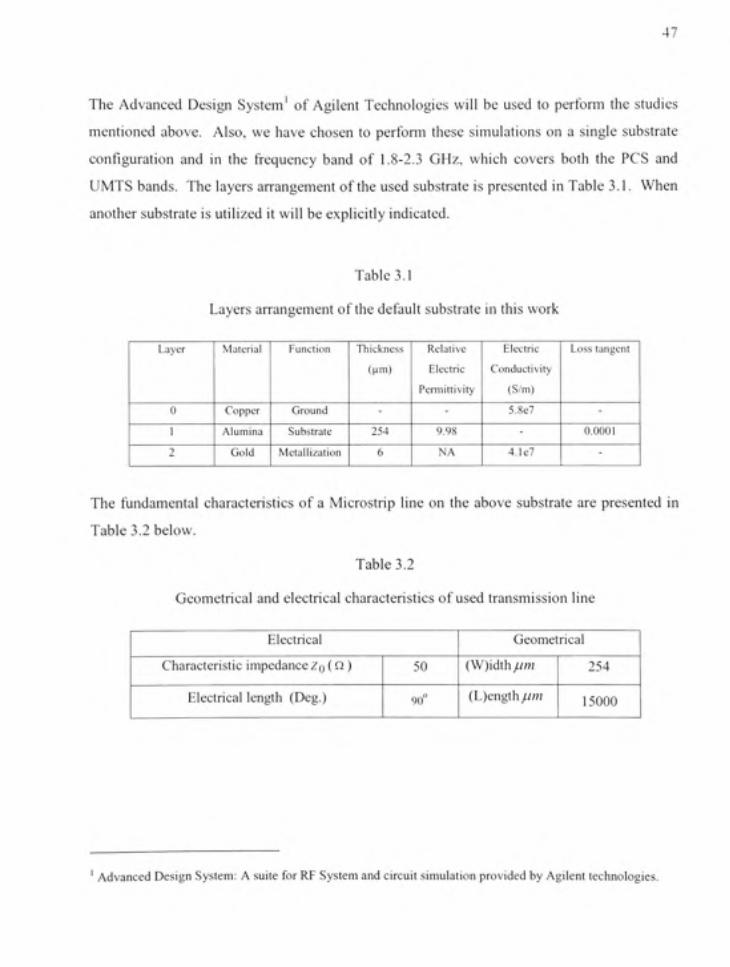
The Advance d Desig n System ' o f Agilen t Technologie s wil l b e use d t o perfor m th e studie s
menfioned above . Also , w e hav e chose n t o perfor m thes e simulation s o n a singl e substrat e
configuration an d i n th e frequenc y ban d o f 1.8-2. 3 GHz , whic h cover s bot h th e PC S an d
UMTS bands . Th e layer s arrangement o f the used substrat e i s presented i n Table 3.1 . Whe n
another substrat e i s utilized i t will be explicitly indicated .
Table 3. 1
Layers arrangement o f the default substrat e i n this work
Layer
0
1
2
Material
Copper
Alumina
Gold
Function
Ground
Substrate
Metallization
Thickness
(Mtn)
-254
6
Relative
Electric
Pennittivity
-9.98
NA
Electric
Conductivity
(S/m)
5.8e7
-4.1e7
Loss tangen t
-0.0001
-
The fundamenta l characteristic s o f a Microstri p lin e o n th e abov e substrat e ar e presente d i n
Table 3. 2 below .
Table 3. 2
Geometrical an d electrica l characteristic s o f used transmissio n lin e
Electrical
Characteristic impedanc e ZQ (O.)
Electrical lengt h (Deg. )
50
90"
Geometrical
(W)idth/v/w
(L)ength/^A«
254
15000
Advanced Design System: A suite for RP System and circuit simulation provided by Agilent technologies .
48
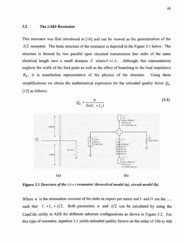
3.2 The X/4±6 Resonator
This resonato r wa s first introduce d i n [16 ] an d ca n b e viewe d a s th e generalisatio n o f th e
Xjl resonator . Th e basic stmcture of the resonator is depicted in the Figure 3.1 below. Th e
stmcture i s forme d b y tw o paralle l ope n circuite d transmissio n lin e stub s o f th e sam e
electrical lengt h sav e a smal l distanc e 5 wher e 5 « X. Although , thi s representatio n
neglects the width o f the feed poin t a s well as the effect o f branching to the load impedanc e
RQ , i t i s nonetheles s representativ e o f th e physic s o f th e stmcture . Usin g thes e
simplifications w e obtai n th e mathematica l expressio n fo r th e unloade d qualit y facto r Q^^
[12] as follows:
(3.1) Qu^ n
2aiL + l^)
W4+5
Zin
W4-5
n MLOC TL2 Subsl='MSubr W=250 urn L=(15000-del)um o
Termi Num=1 Z=50 Ohm
Croil Sub t-W1 W2 W3 W4
OS-', . R l • R=50 Ohm
•MSubr 250 urn 250 um 250 um 250 um
D Subst='MSubr W=250 um L=(15000+del)um
(a) (b )
Figure 3.1 Structure of the A/4 ± S resonator: theoretical model (a), circuit model (b).
Where a i s the attenuation constan t of the stubs in nepers per meter and 1- and 1+ are the ... .
such tha t /_+/+ = /1/2 . Bot h parameter s a an d /1/ 2 ca n b e calculate d b y usin g th e
LineCalc utilit y i n AD S fo r differen t substrat e configuration s a s show n i n Figur e 3.2 . Fo r
this type of resonator, equation 3.1 yields unloaded quality factors on the order of 10 0 to 400

49
for typica l commerciall y availabl e substrate s o f differen t metallizatio n thicknesse s an d
dielectric constants.
File Sirfiul.3tio n Option s Hel p
Component
'^VP^ MLI N
Substrate Parameters
MSUB DEFAUL T
Er
Mur
H
Hu
T
Cond <
2.330
1000
787.000
3.9e+34
35 000
R iae7
Component Parameters
-teq
Wain
Waie
2 000
MUN: MLIH DEFAUL T
Physical
W
L
um
mil
um
GHz -r :
.mil • I
I mil
/
Synthes
Elec
ZO
E_Eff
2289 770000
53513 700000
ize
a lical
50 000
180000
um - ^
um •^1
—i 1 I
Analyze
H Ohm
deg • »
r !
' • - — ^
./1 / KwH
Calculated Result s
K_Eff = 1 9B 1 A_DB = 0 03B SkinDepth = 1 5G3u m
Values are consistent
Figure 3.2 LineCalc showing resonator loss as ADB.
On the other hand, the loaded quality factor Qi o f this resonator has different characteristics .
To calculat e th e loade d qualit y facto r o f thi s resonato r w e wil l us e th e result s o f circui t
simulafion o f the circuit of Figure 3.1. Th e loaded quality factor ca n be calculated from the
magnitude of the input impedance Z, „ curv e using the following formula :
Qi = fo ^hdb
(3.2)
50
Where / ^ i s th e resonanc e frequency (wher e Z, „ attain s it s maximu m valu e fo r th e
configurafion use d above) and A/3^ ^ i s the bandwidth where |Z,„ | <|Z,„|^^^/V2 o n the Z, „
curve. Figure 3.3 illustrates the variation of |Z,„ | o r mag(Zin) with the frequency for severa l
values fo r th e fee d poin t displacemen t "6" . I n Figur e 3. 4 th e loade d qualit y facto r Q L i s
presented a s a function o f the feed poin t displacement, values for Q L are calculated from the
values presented in Figure 3.3.
40 hli^siirinlnr Irsfiij l Itripciinnci ;
a!) -
'JO
25
^^n
15
10
. • • • " . ^ ' '
y
. • • • • • , ' • ' / ' 1- , '
. ' • ' ' .y / -•" " * '''^
y ; _ / :
. . ."l^s . X ? 1 .,
S X > .
\ . ^ ' • ^ . X V s
V , ' • • - . , _
6 (um ) nn n
= 900 = 12UU = 150D = 10UU = 21UU 210U
1.9 1.U 2 i.y- t i.yt > I req
1 ya X 1 1
Figure 3.3 Magnitude of input impedance vs frequency for different values of 6.

51
3 0 1 I I : I ?iin 401 1 firm nn n inn n i?ri n nn n ifio n
6(*l l ie H m)
Figure 3.4. Q/ vs S.
From Figur e 3.4 abov e i t i s clear tha t th e loaded qualit y facto r increase s as 6 approaches to
zero. The variatio n i s quite linea r i n genera l whic h i s very convenien t fo r tunin g purposes .
Figure 3.3 give us another insight into the inner-workings of this resonator: as the value of S
is decrease d t o achiev e highe r Qi, the magnitud e o f th e inpu t impedanc e a t th e resonato r
decreases. Fo r example , a quality facto r i n th e orde r o f 9 0 i s achieve d a t 6-300 /um. For
(5=:300//m, we find that mag(Zi„) ~3 a t the resonance frequency , a s can be seen from Figure
3.3 . Consequentl y a higher Qi is achieved at a high retum loss.
As w e hav e see n i n thi s section , th e A/4±S resonato r allow s fo r increasin g th e loade d
quality factor by changing the displacement o f the feed poin t of the resonator . An d we have
demonstrated tha t this increase is achieved a t high retum loss values for the resonator. I n the
next section we will use this resonator to design two types of second order filters. Thes e will
be th e startin g filter stmcture s o n whic h w e wil l appl y th e geometrica l optimisatio n o n t o
achieve miniaturisation.

52
3.2.1 Secon d order band-bass filters using X/4±6 resonators
In this sectio n w e wil l analyz e the behaviour o f two second orde r filter stmctures . W e will
use the electromagneti c simulatio n too l Momentu m t o analyz e th e respons e o f these filters
and to analyze their response to perturbations of design parameters. I n general our procedure
is to perform a parameter swee p fo r eac h desig n parameter , i.e . the parameter o f interes t i s
varied whil e al l other s ar e fixed. This proces s i s repeated fo r eac h parameter , subsequentl y
according to the obtained results the response of the filters is analysed.
3.2.2 Symmetri c Feed Structure
The symmetri c fee d poin t stmctur e i s composed o f two identica l resonator s separate d b y a
distance X suc h that they are electromagnefically couple d alon g the length of the resonator.
Moreover, th e fee d poin t fo r each resonator i s displaced i n the same direction fro m th e mid
point of the resonator as illustrated in Figure 3.5 below.
A similar filter stmcture t o the one presented above , has been thoroughl y discusse d i n [17] .
The autho r i n [17 ] demonstrate d theoreticall y tha t thi s stmctur e exhibit s a finit e frequency
zero i n it s lowe r transmissio n band , an d tha t th e zeros ar e not du e to cros s couplin g o f the
resonators. Rather , the transmission zeros are due to intemal ant i resonance in the stmcture.
This fact i s advantageous fo r miniaturization purposes , as it allows simultaneously, the use of
only tw o resonator s t o realis e a filter an d th e insertio n o f transmissio n zero s i n th e filter
response. Th e autho r i n [17 ] ha s use d th e fee d line s widths ' an d lengths ' t o resolv e finit e
frequency transmissio n zeros for both of these stmctures.
The filter stmctures w e have starte d wit h ar e almost identica l t o the ones presented i n [17],
the main differenc e i s the inpu t fee d an d outpu t transmissio n line s ar e assumed t o be shor t
and matched. Thi s way these lines are not used in our case to resolve additional zero s or to
enhance the retum los s of the filter in contrast t o what was done in [12] . W e have imposed
53
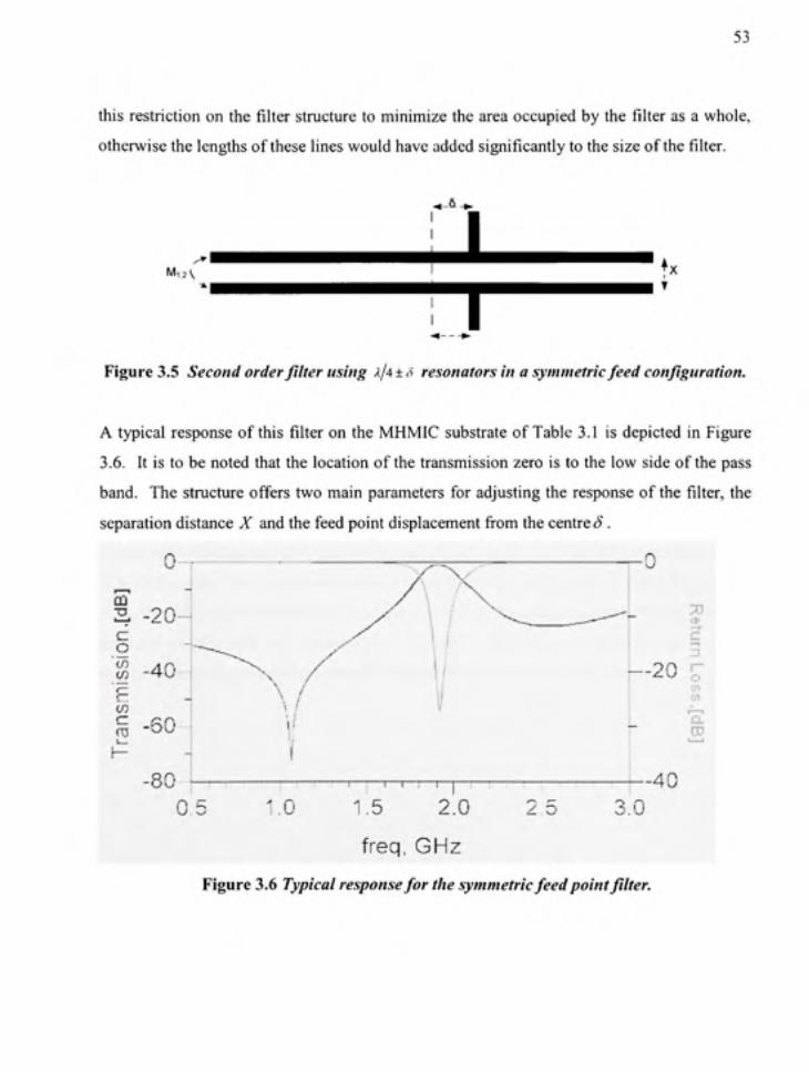
this restriction o n the filter stmcture to minimize the area occupied b y the filter as a whole,
otherwise the lengths of these lines would have added significanfiy t o the size of the filter.
^ _ & .
M l 2 ^
T Figure 3.5 Second order filter using A/4 ± S resonators in a symmetric feed configuration.
A typical respons e of this filter on the MHMIC substrat e of Table 3.1 i s depicted i n Figure
3.6. I t is to be noted tha t the location of the transmission zer o is to the low side of the pass
band. Th e stmctur e offer s tw o main parameter s fo r adjustin g th e response of the filter, the
separation distance X an d the feed point displacement from the centred .
freq, GH z
Figure 3.6 Typical response for the symmetric feed point filter.
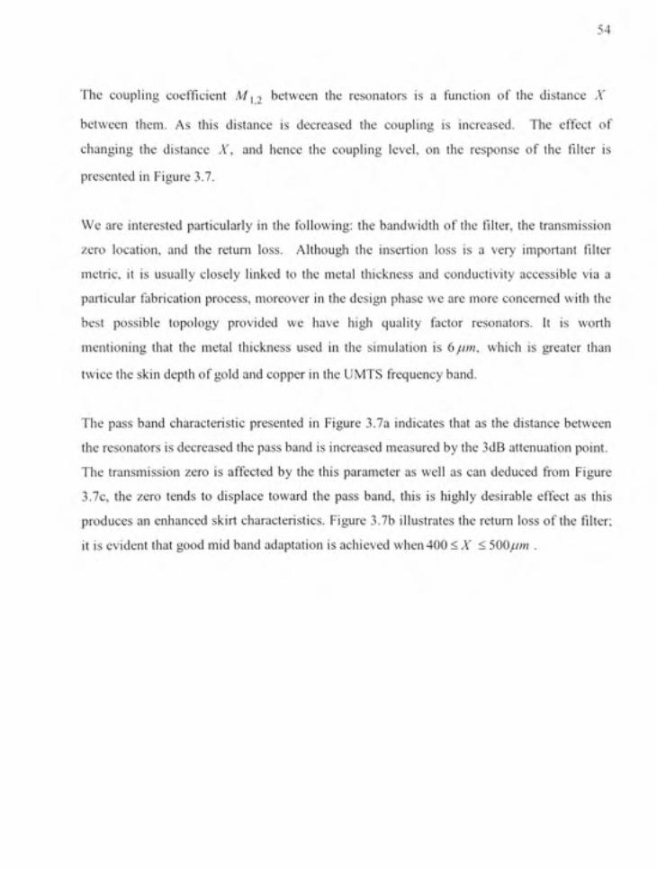
54
The couplin g coefficien t M , 2 betwee n th e resonator s i s a functio n o f th e distanc e X
between them . A s thi s distanc e i s decrease d th e couplin g i s increased . Th e effec t o f
changing th e distanc e X, an d henc e th e couplin g level , o n th e respons e o f th e filter i s
presented i n Figure 3.7 .
We ar e intereste d particularl y i n th e following : th e bandwidt h o f th e filter, th e transmissio n
zero location , an d th e retu m loss . Althoug h th e insertio n los s i s a ver y importan t filter
metric, i t i s usuall y closel y linke d t o th e meta l thicknes s an d conductivit y accessibl e vi a a
particular fabricatio n process , moreove r i n the desig n phas e w e ar e mor e conceme d wit h th e
best possibl e topolog y provide d w e hav e hig h qualit y facto r resonators . I t i s wort h
mentioning tha t th e meta l thicknes s use d i n th e simulatio n i s 6///?7 , whic h i s greate r tha n
twice the skin depth o f gold an d coppe r i n the UMTS frequenc y band .
The pas s ban d characteristi c presente d i n Figur e 3.7 a indicate s tha t a s th e distanc e betwee n
the resonators i s decreased th e pass band i s increased measure d b y the 3dB attenuation point .
The transmissio n zer o i s affecte d b y th e thi s paramete r a s wel l a s ca n deduce d fro m Figur e
3.7c, th e zer o tend s t o displac e towar d th e pas s band , thi s i s highl y desirabl e effec t a s thi s
produces a n enhance d skir t characteristics . Figur e 3.7 b illustrate s th e retu m los s o f the filter;
it is evident tha t good mid band adaptatio n i s achieved whe n 400 < A' < 500/jm .

55
;• L L j i i
>;=infi '4r\
X-tUL . r 1
Figure 3.7 Effect of spacing on: transmission (a), matching (b), and zero location (c).
The second paramete r i s the displacement o f the fee d poin t from the centre of the resonator
denoted i n Figur e 3. 8 b y "6" . Th e swee p result s i n Figur e 3.8 a indicate s tha t whe n th e
displacement i s decreased the attenuation nea r the pass band is increased. Whil e this is very
desirable, i t i s unfortunately achieve d a t th e expense o f significan t ripples appearin g i n th e
pass band. I n addition, it is also obvious that the zero tends to approach the pass band as '"d"
is decreased . Th e matchin g characteristic s als o sho w dramati c variatio n whe n "6 " i s
decreased belo w 2500 fum. This can be attributed to the increase of the loaded qualit y facto r
of each resonato r t o the extent tha t th e resonators ar e strongly couple d onl y a t the two spli t
resonance frequencies .
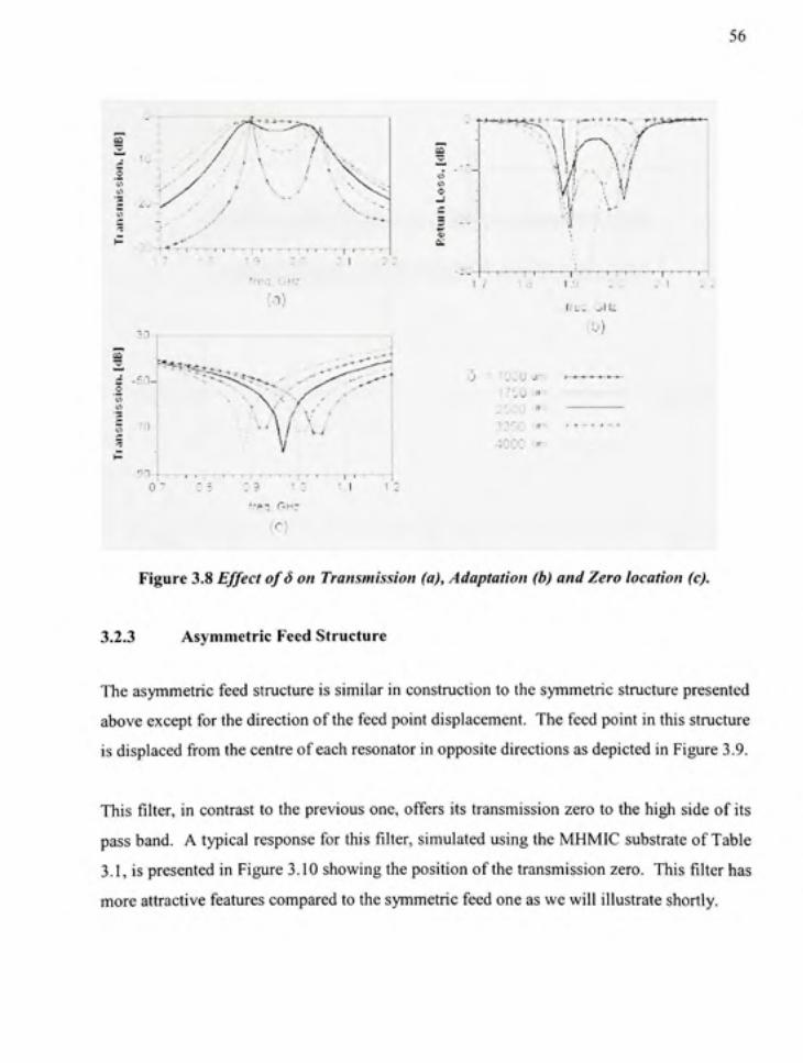
56
"0
Z ^- ^
i .' 0
-90-
ht--».
v , ,-~.p. . ,..™.f-^™^~.^™,~,~.,r..y..j..... . ,....r~.J-~.......... .
0 ? O S D, 9 1 0 5. 1 1 2 --P-; r--- -
'C'l
4>
• \
0 - 100 0 lifr . 1750 -2GC0 " 3250 '." -4000 -'r -
\0)
Figure 3.8 Effect of 6 on Transmission (a), Adaptation (b) and Zero location (c).
3.2.3 Asymmetric Feed Structure
The asymmetric feed stmctur e is similar in constmction to the symmetric stmcture presented
above except for the direction of the feed point displacement. Th e feed point in this stmcture
is displaced from the centre of each resonator in opposite directions as depicted in Figure 3.9.
This filter, in contrast t o the previous one, offers it s transmission zer o to the high sid e of its
pass band. A typical response for thi s filter, simulated using the MHMIC substrate of Table
3.1, is presented i n Figure 3.10 showing the posifion o f the transmission zero . Thi s filter has
more attractive features compared to the symmetric feed one as we will illustrate shortly.
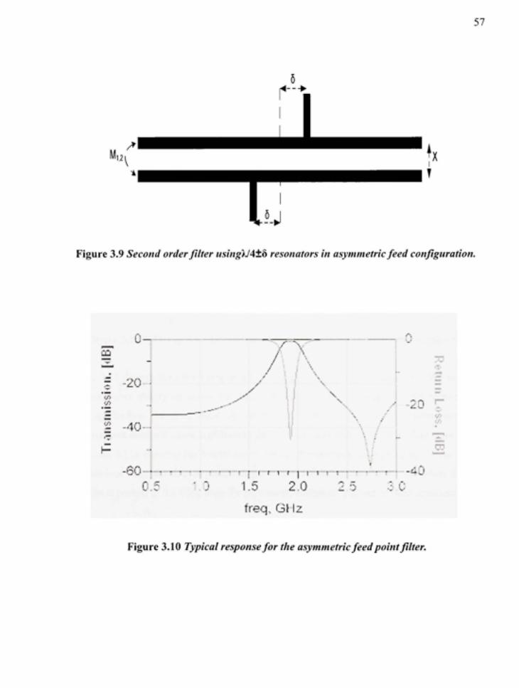
57
Figure 3. 9 Second order filter using'U4±d resonators in asymmetric feed configuration.
iXi
v>
•J-.'
n
—
-20
-40-
0^5 i"o
/ ' . i ' \
y \\ \ . ^ 1
r
r\
''X'
••20 g -
1 r
1"'"T j - " - ( - - r • 7 r I ' l i ' i - ' • ' •• • ! • -r<j
1.5 2. 0 2 5 3 C
freq, G\ \z
Figure 3.1 0 Typical response for the asymmetric feed point filter.

58
CO
2 ' «
JJ . , . , J , , 17 - 0 - 5 2
I T I ' T ? r I I I T T • I 1" ^ • ] 4)
7 1
rroq GH 2
n—I———T—I—'-^'—r-ri"'"^—i—r"^'~i~
1 7 • ;- 1 1 - 9 1" . .• > •
T e q , G - . ; 4l>)
5 i j i " i ) = * c o ' -»--•-*- — :>'":n' ;'.niif .,•0-1-1 _ _ _ ^
n • i n freq C-H z
Figure 3.11 Effect ofS on Transmission (a), Return Loss (b) and Zero location (c).
Figure 3.11 depicts the filter's response to varying the feed poin t distance "5" . W e note that
this paramete r clearl y enhance s th e skir t characteristic s o f th e filter sinc e th e transmissio n
zero approache s th e pas s ban d o f th e filter a s "S " i s decreased . Furthermor e thi s
enhancement doe s not cause significant ripples in the pass band. This i s evident fro m Figur e
3.11a and 3.11c showing the transmission an d the transmission zer o location. I n contrast t o
the previous filter th e ripples produced ar e within 1. 2 dB in th e whole band whe n th e zer o
location is pushed to 0.3 GHz from the pass band to achieve high out of band attenuation .
From Figure 3.1 Ic we can see the variafion o f the input matching of the filter. Th e mid band
matching change s significantl y a s a resul t o f varyin g th e fee d poin t "8" . However , thi s
variation i s acceptable compared t o that o f the symmetric fee d poin t stmcture . Finally , i t i s
to be noted that the bandwidth of the filter is practically unchanged i n response to a sweep in
the feed point distance '5' as can be seen in figure 3.12.

59
I—
O 'co
CO I—
CO H
0-6 i ^ n : ^ -1. 1
freq. GHz
Figure 3.12 Effect of 6 on Zero location showing an unresolved zero.
Another highly attractive feature of this filter stmcture is the existence of an unresolved zer o
to the lo w sid e of the pass band. Th e unresolved zer o i s highlighted i n Figure 3.12 , where
the attenuation to the low side of the pass band is dramatically improved a s "S"" is decreased.
This transmissio n zer o ca n b e resolve d usin g th e lengt h o f th e fee d line , however , w e
indicated previously , w e have opted no t t o use this technique i n an effort t o miniaturise th e
filter. Late r on , w e wil l demonstrat e anothe r techniqu e t o resolv e thi s zer o whil e
miniaturising the filter at the same time.
The response of the filter to the variation o f the distance X between the resonators i s shown
in Figure 3.13. Th e bandwidth of the filter increases as the distance between the resonators is
decreased similarl y to the symmetric feed stmcture , but the transmission zero location hardly
changes.
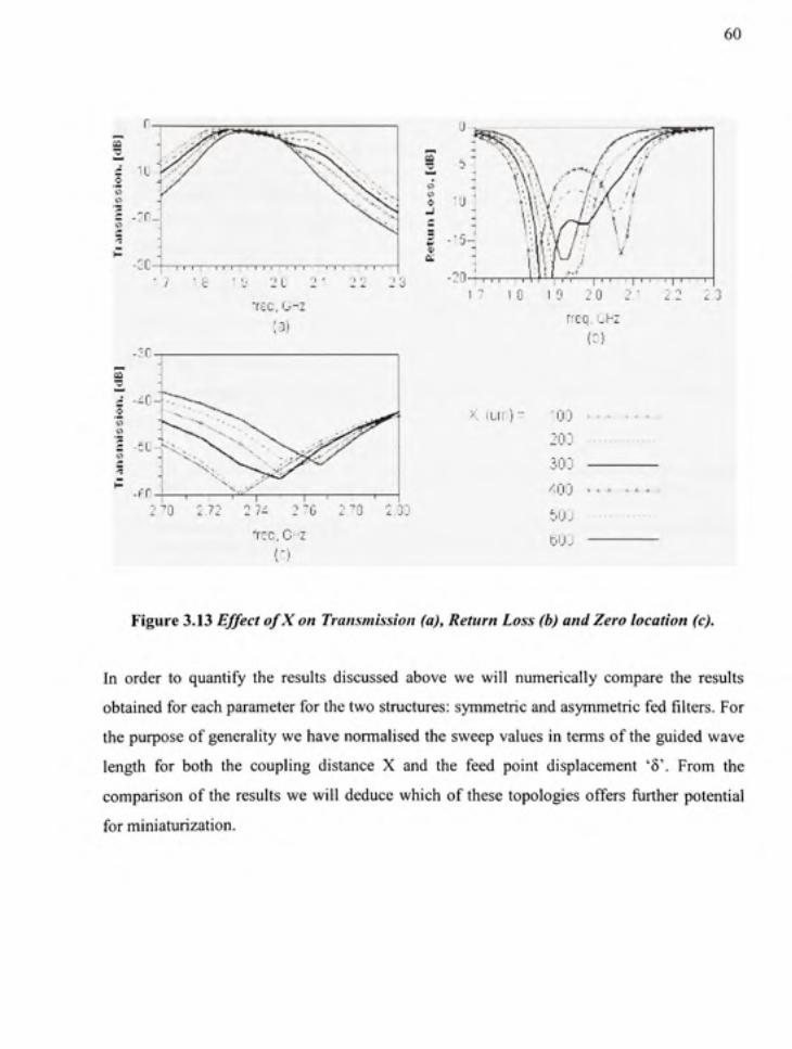
60
ta
0
-GO- —r—i—r^ r~ n •—n~ i TT—i——r -
T t C , U - 2
-r-r-CQ
=• - i O - J ^
£ -£C -
-(^r 2 " 0 2.7 2
2 3
" • \- " l • • • / • • , / ' ' " " 1
1) u
>: i L i r ) - • | J ; J V * .* , .4, .* . A ,.
5UJ
Figure 3.13 Effect ofXon Transmission (a), Return Loss (b) and Zero location (c).
In orde r t o quantif y th e result s discusse d abov e w e wil l numericall y compar e th e result s
obtained for each parameter for the two stmctures: symmetric and asymmetric fed filters. For
the purpose of generality we have normalised the sweep values in terms of the guided wav e
length fo r bot h th e couplin g distanc e X an d th e fee d poin t displacemen t '5 ' . From th e
comparison o f the results we will deduc e which o f these topologie s offer s furthe r potentia l
for miniaturization .

61
Table 3.3
Sweep range for filters' design parameters
Parameter
X
8
Sweep Rang e
Physical Lengt h ( /um )
100 to 600
1000 to 4000
Referred t o X
0.0033/1 to 0.02A
0.033/Lto0.13/l
Electric Length " (A
0.6° to 3.6°
6° to 23.4°
In Tabl e 3. 4 w e summariz e th e result s obtaine d fo r th e presente d stmctures . Fro m th e
arguments presente d abov e an d th e result s presente d i n th e Tabl e 3.4 , w e observ e th e
following:
- Th e variafion o f X has a n incidence o n th e bandwidth fo r th e asymmetri c stmcture , while it affects th e bandwidth and the zero location for the symmetric stmcture.
- Decreasin g "8 " enhances th e skir t attenuatio n fo r both stmctures , but come s with an unacceptable ripple in the pass band for the symmetric stmcture.
- Th e fee d poin t displacemen t "8 " of ha s stron g incidenc e o n th e transmissio n zer o position an d skir t characteristi c an d negligibl e effec t o n th e bandwidt h i n th e asymmetric stmcture.
- Filte r retum loss is sensitive to both parameters.
It is evident from the above analysis that the asymmetric stmcture offers bette r performanc e
potential. Th e contro l ove r th e asymmetri c stmctur e usin g desig n parameter s i s relativel y
straightforward a s each design parameter mainly affects on e of the performance metrics . A n
added featur e o f the asymmetric stmcture is the extra unresolved zer o in to the lower side of
• The electrical length measures the physical length relative to the length of the electromagnetic wav e in degrees

62
the bas s band ; a featur e tha t greatl y enhance s th e skir t characteristi c o f th e filter.
Consequently, the asymmetric feed stmcture is chosen fo r further study .
Table 3.4
Symmetric versus asymmetric feed response to parameter sweep
Metric
Bandwidth Absolute MH:
Fractional %
Transmission zero freq GHz
Skirt attenuation' dB
Retum loss dB
X(/Jm )
Min
100
Sym.
333
16
1.25
7
-6
Asym.
342
17.6
2734
8
-5.7
Ma.x
600
Sym.
130
6. 5
0.8
9
-20
Asym.
154
7.7
2.766
8
-18
5 ( /y/ H )
1000
Sym.
154
7.7
1.0
23
-0.1
Asym.
168
8.4
2 3 7
14.6
-3.3
4000
Sym.
186
9. 3
0.88
8
-25
Asym.
158
7.9
3. 13 8
5
-7.7
3.2.4 Topological Optimizatio n
In th e previou s sectio n w e hav e chose n th e asymmetri c filter stmctur e fo r furthe r
optimization. Th e technique of topological opfimisafion wa s introduced i n [8] and applied to
a squar e filter topology . I t consist s o f findin g a mor e compac t topolog y usin g
electromagnetic simulatio n an d heuristi c optimisation . Althoug h thi s techniqu e i s difficul t
and time consuming, especially in the early phases of the design, i t results in compact filters
with excellen t performanc e a s demonstrate d i n [8 ] an d i n thi s curren t work . On e o f th e
difficulties wit h th e topologie s introduce d i n [8 ] i s tha t ther e i s n o clea r methodolog y fo r
^ The attenuation is evaluated at lOOMH z from the 3dB point
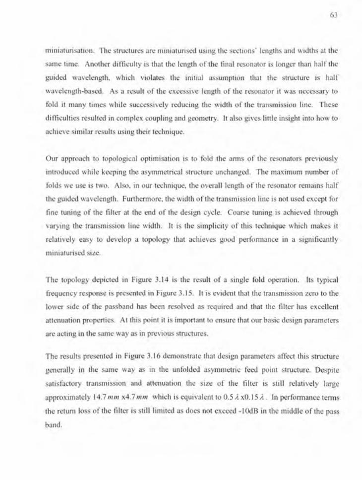
63
miniaturisation. Th e stmctures are miniaturised usin g the sections' length s and widths at the
same time. Anothe r difficulty i s that the length o f the final resonator i s longer than hal f the
guided wavelength , whic h violate s th e initia l assumpfio n tha t th e stmctur e i s hal f
wavelength-based. A s a result o f the excessiv e lengt h o f the resonator i t was necessar y t o
fold i t man y time s whil e successivel y reducin g th e widt h o f th e transmissio n line . Thes e
difficulties resulte d in complex coupling and geometry. I t also gives little insight into how to
achieve similar results using their technique.
Our approac h t o topologica l optimisatio n i s t o fol d th e arm s o f th e resonator s previousl y
introduced whil e keeping the asymmetrica l stmctur e unchanged . Th e maximum numbe r o f
folds w e use is two. Also , in our technique, the overall lengt h of the resonator remains half
the guided wavelength. Furthermore , the width of the transmission line is not used except fo r
fine tuning o f th e filter a t th e en d o f th e desig n cycle . Coars e tunin g i s achieve d throug h
varying th e transmissio n lin e width . I t i s th e simplicit y o f thi s techniqu e whic h make s i t
relatively eas y t o develo p a topolog y tha t achieve s goo d performanc e i n a significantl y
miniaturised size.
The topolog y depicte d i n Figur e 3.1 4 i s th e resul t o f a singl e fol d operation . It s typica l
frequency respons e i s presented in Figure 3.15. I t is evident that the transmission zero to the
lower sid e o f th e passban d ha s bee n resolve d a s require d an d tha t th e filter ha s excellen t
attenuation properties. A t this point i t is important to ensure that our basic design parameters
are acting in the same way as in previous stmctures.
The results presented i n Figure 3.16 demonstrate tha t desig n parameter s affec t thi s stmctur e
generally i n th e sam e wa y a s i n th e unfolde d asymmetri c fee d poin t stmcture . Despit e
satisfactory transmissio n an d attenuatio n th e siz e o f th e filter i s sfi U relativel y larg e
approximately \A.l mm xA.lmm whic h is equivalent to 0.5/1x0.15/1. I n performance term s
the retum los s of the filter is sfill limite d as does not exceed -lOdB in the middle of the pass
band.

64
Figure 3.14 First iteration of topological optimisation.
CD — -20 -o
4 0 H
•m-
•8U
\ I
y \ /
T 1 1 1 1 1
10 1 5 1 r
n
-; j
-10
-15
A-/ * ^ c —! 3 r" o */* <,•>
m •20
.0 ,0
Freq^r^ncy [GHz ]
Figure 3.15 Transmission and return loss response of the topology in Figure 3.14.

65
Bandwidth increas e
^
'6' increas e
freq, GHz
rn~n"n~n~n~n~n~n~r-n~n 141 .51 61.71.3 1 9 2 . 0 2 . 1 2 . 2 2 3 2 . 4 2 5 2 . 6
freq, GHz
Figure 3.16 Response of the filter as a function of design parameters sweep.
t E
•8.8 mm -
Figure 3.17 Geometrically optimized filter structure: doubly folder with asymmetric feeds.
Using the same miniaturisation techniqu e we proceed wit h foldin g th e filter arms to achieve
fiirther miniaturization o f the stmcture. The resulting stmcture is depicted in Figure 3.17, the
size of the stmcture i s now reduced b y almost 50 % to 0.06/1x0.14/1 . Th e intemal arm s o f
this stmcture provide additional paths between the input and output of the filter. Thes e paths

66
have resulted in an additional zero in the filter response as highlighted in the figure 3.18. I t is
clear tha t th e attenuatio n characteristic s t o th e hig h sid e o f th e pas s band , wher e th e extr a
zeros ar e located , ar e greatl y enhanced . Thi s performanc e enhancemen t ha s com e wit h a
price, namely a difficulty i n finding the opfimal solufio n an d a difficulty o f maintaining good
retum loss for a given bandwidth and skirt attenuation requirements.
The difficult y i n maintaining suitabl e retu m los s stem s fro m th e fac t tha t th e retum los s i s
sensitive t o bot h ou r desig n parameter s th e separatio n distanc e betwee n resonator s an d th e
feed poin t displacements . Thi s proble m ha s been illustrate d earlie r whe n w e presented th e
basic filter stmcture s i n section . I n the nex t sectio n w e presen t a stmcture tha t offer s a n
additional degree of freedom for adjusting the retum loss.
CD
d
'<n CD
cz CO
0-
-20-
•40-
•ou-
A , \ Additiona l
/ ' ' \ Zeros
- i — I — I — I — I — I — I — 1 — I — I — I — i — I — I — | -
1.0 1.5 2.0
Frequency
•"•> 5 I r
•0
- ' • )
-25 •J-
C 3 r-o
rfl
Figure 3.18 Transmission and return loss response of the topology in Figure 3.17.

67
3.2.5 Modified por t structure
The retum los s o f the miniaturize d stmctur e suffer s fro m poo r controllability , whic h stem s
from retum loss sensitivity to design parameters. Thi s results in reduced degrees of freedom
per performance metric . I n order to better understand th e problem and the stmcture we have
constmcted a thre e dimensiona l mode l (Figur e 3.19 ) o f th e miniaturize d stmctur e usin g
EMDS t o analyse the flow of energy in the stmcture. I n three dimensional electromagneti c
modeling an d simulation , i t i s very important fo r th e accuracy an d validity o f the results to
reach a mesh tha t properl y capture s the variation o f the electromagneti c field a t the desired
frequency. W e hav e use d th e adaptiv e mes h refinemen t utilit y availabl e i n EMD S whic h
enables us to progressively achiev e a good mesh . A mesh i s considered goo d whe n a good
compromise between the memory and accuracy requirements has been attained.
Figure 3.19 3-Dimensional doubly folded filter model in EMDS.
EMDS is a three dimensional model capture and electromagnetic simulato r provided by Agilent
68
In order to insure that our Momentum simulatio n (2.5D) captures properly the physics of our
stmcture we have compared i t to the 3D model simulation results obtained from EMDS . Th e
comparison i s depicted i n Figure 3.20. W e notice that excellen t agreemen t between th e two
models i s obtained . Thes e result s giv e u s confidenc e tha t th e 2.5 D simulafio n obtaine d
through Momentum is good compromise between the simulation time and accuracy.
Once th e thre e dimensiona l mode l i s properl y meshe d an d simulate d w e use d th e
postprocessor engin e to calculate and display the poynting vecto r to analyse energy flow in
the filter stmcture. Th e mesh and the poynting vector distribution ar e shown i n figure 3.21.
From thi s figur e w e ca n se e tha t th e poynting vector' s intensit y i s maximum i n th e folde d
arms next to the gap between the resonators. W e also note that the retum loss problem lies in
the inefficient por t stmcture that has a low energy transfer a s indicated by small arrow size in
the right figure. Thi s has led us to conclude that, in order to improve the filter retum loss, we
need t o find a better por t stmctur e to couple energy more efficiently t o the intemal arm s of
the resonators.
To the end o f better retum loss , we propose to modify th e port stmctur e a s shown i n figur e
3.22. Instea d o f th e standar d 50 Q transmissio n lin e feed , w e introduc e a smal l sectio n o f
lower characteristi c impedanc e transmission line , i.e., a section wit h a wider line . T o asse s
the impact of this line's width, i.e. the parameter Y, on the filter response we proceed with a
parametric study similar to the previous ones conducted on resonator spacing and feed offset .
'Poynting vecto r i s calculate d fro m th e electri c an d magneti c fields a s follows : 5=-|||£'x// * wher e S i s th e
apparent or complex power

69
Figure 3.20 Momentum (2.5D) vs EMDS (3D) simulation results.
^ ^ ^ > i R B H I I M ^SSS I D HHI 'D
^^H '
1 1
i 111
1 1 if i
5 ^ ^ ^
9
HH IBM 9
(a) Model mesh (b ) Poyting vector distributio n
Figure 3.21 (a) the mesh used (b) the Poynting vector distribution at 1.96GHz.
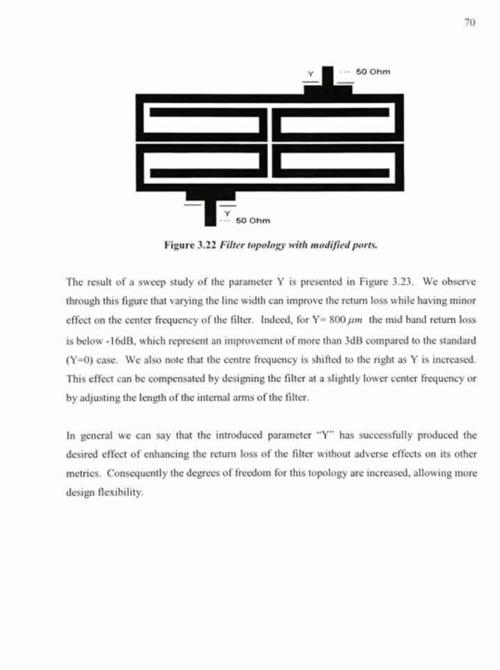
70
50 Oh m
50 Oh m
Figure 3.22 Filter topology with modified ports.
The resul t o f a swee p stud y o f th e paramete r Y i s presente d i n Figur e 3.23 . W e observ e
through thi s figur e tha t varying the line width can improve the retum los s while having mino r
effect o n th e cente r frequenc y o f the filter. Indeed , fo r Y = 80 0 /Jm th e mid ban d retu m los s
is below -16dB , which represen t a n improvement o f more than 3d B compared t o the standar d
(Y=0) case . W e als o not e tha t th e centr e frequency i s shifte d t o th e right a s Y i s increased .
This effec t ca n be compensate d b y designing the filte r a t a slightly lowe r cente r frequency o r
by adjusting th e length o f the intemal arm s of the filter.
In genera l w e ca n sa y tha t th e introduce d paramete r "Y " ha s successfull y produce d th e
desired effec t o f enhancin g th e retu m los s o f th e filter withou t advers e effect s o n it s othe r
metrics. Consequentl y th e degrees of freedom fo r thi s topology ar e increased, allowin g mor e
design flexibility.

71
1/
a. •iU • ,
.2 1
- > •.*. •
Ir-q.L-H.:
-^ I. )
r :un i - j
• ;L!ri j : : iUC
V(l;T,|- d.1I J
Y (UT) - ' I JU
V u r i ! - o.: i
Zeros almos t
unaffected
-.'OC. vVIV
Figure 3.23 Filter response to variation of port width (Y) for the topology in Figure 3.22.
To illustrat e th e ne w desig n technique , a n optimize d receiv e ban d filter fo r UMT S use r
terminal profil e i s designed an d it s response i s presented i n Figure 3.24. Th e attenuation i n
the middle of the transmission band , at 1.94GHz , is -33dB and the insertion los s is -2.36 dB
while the retum los s is better than -15dB. Th e size of this filter is 3.9mmx9.2mm whic h i s
40% smaller than filters reported in [8].
CD -D C o (/) (/) F 1/) d TO
1 -
0
- 9 0 -
i
-411-
-60-1
\ / ^ ~ \ f
/ 1 \ / • ' \
>y / , ' \ \ / 1 ' ^ \ V i \r~y.
1 . 1 . I 1 1 1 6 1. 3 2. 0 22 2. 4 2
Frequency [GHz ]
n
" " - - ' ,"T 1
-». - 1 0 =
r~ --15 i
' r^ — 90 T '
- 2 5 6
Figure 3.24 Filter response of the topology in Figure 3.22.
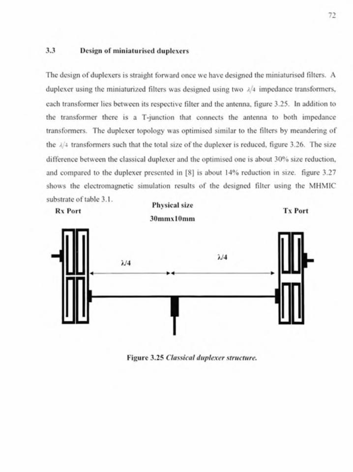
72
3.3 Design of miniaturised duplexers
The design of duplexers is straight forward onc e we have designed the miniaturised filters. A
duplexer using the miniaturized filters was designed using two A/4 impedance transformers ,
each transformer lie s between it s respective fdter an d the antenna, figure 3.25 . I n addifion t o
the transforme r ther e i s a T-junctio n tha t connect s th e antenn a t o bot h impedanc e
transformers. Th e duplexer topolog y wa s optimised simila r t o the filters by meandering o f
the A/4 transformer s suc h that the total size of the duplexer is reduced, figure 3.26 . Th e size
difference betwee n the classical duplexer and the optimised one is about 30% size reduction,
and compare d t o the duplexe r presente d i n [8 ] i s about 14 % reducfion i n size , figure 3.2 7
shows th e electromagnefi c simulatio n result s o f th e designe d filter usin g th e MHMI C
substrate of table 3.1. Physical size
Rx Port T x Port
-n Physical size
30mmxl0mm
yj4 ^14
- * • • * -
Figure 3.25 Classical duplexer structure.

73
Ant Por t
Rx Port I
\h
Physical size
14.5mmxl4.5mm
Tx Por t
Figure 3.26 Topologically optimized duplexer structure.
CD •o
0) S -1C H
•S - 1 ! cn
-2a
Tx R x Band Ban d
- ] — I — I 1—I—1—I—I—I—I— I 1 I I I r -
1.6 1. 7 1. 8 1 9 2. 0 2. 1 2. 2 2. 3 2. 4 2. 5 freq, GHz
Tx R x Band Ban d
GQ 2 , -20 -
E -40 -
-60-
-80-
Nf- \
- r 1 — 1 — 1 — I — 1 — 1 — I — r ~ " i — r — ' — i — i — i — • — 1 8 1 7 1 8 1 9 2. 0 2. 1 2. 2 2. 3 2. 4 2
freq, GHz
-20
-40
-60 ro
.-80
Transmission
Figure 3.27 Optimised duplexer response (Left) Return loss, (Right) Transmission.

74
This se t of results demonstrates excellen t performance an d miniatunzation whe n compared t o
the state of the art i n the field.
3.3.1 Fabricatio n result s o n MHMIC proces s
3.3.1.1 Introductio n
In thi s sectio n w e wil l presen t th e measure d result s followin g fabricatio n o f th e filters an d
duplexers tha t wer e designe d usin g ou r propose d techniqu e usin g a MHMI C proces s
substrate. Al l fabricate d filters an d duplexer s wer e measured usin g the Wirltron fixtur e ki t t o
avoid packagin g the circuit s an d addin g connector s t o them. Measurement s wer e taken usin g
the Agilen t Vecto r Networ k Analyse r afte r a TRL calibrafio n procedur e [18] . Th e MHMI C
substrate used i n the fabrication proces s has the following properties :
Substrate thickness 10 mil +/- 5% Relative permittivity (£•,. ) 9.9 Loss tangent 0.000 1 Relative permeability 1 Roughness ~ 1 |i m Maximum circui t siz e .9" x .9" Conductor thickness 1 |am Metal conductivit y (Gold ) 4.1e7 S/ m
We can estimate the mid band filter los s theoretically o n thi s substrate fo r th e frequency ban d
of interest by applyin g
Q « (3.1 )
and th e following equatio n fro m [19] :
^Qu
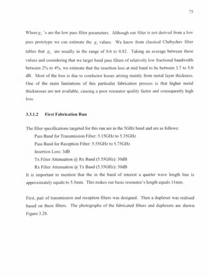
75
Whereg, ' s ar e the low pass filter parameters. Althoug h ou r filter is not derived from a low
pass prototyp e w e ca n estimat e th e g^ values. W e kno w from classica l Chebyche v filter
tables tha t g , ar e usuall y i n th e rang e o f 0. 6 t o 0.82 . Takin g a n averag e betwee n thes e
values and considering that we target band pass filters of relatively low fractional bandwidth
between 2 % to 4%, we estimate tha t the insertion los s at mid band t o be between 3. 7 t o 5. 0
dB. Mos t o f the loss i s due to conducto r losse s arisin g mainly fro m meta l laye r thickness .
One o f th e mai n limitation s o f thi s particula r fabricafio n proces s i s tha t highe r meta l
thicknesses ar e not available , causing a poor resonato r qualit y facto r an d consequentl y hig h
loss.
3.3.1.2 Firs t Fabrication Run
The filter specifications targete d for this mn are in the 5GHz band and are as follows:
Pass Band for Transmission Filter : 5.15GHz to 5.35GHz
Pass Band for Reception Filter : 5.55GHz to 5.75GHz
Insertion Loss : 3dB
Tx Filter Attenuation (g Rx Band (5.55GHz): 30dB
Rx Filter Attenuafion @ Tx Band (5.35GHz): 30dB
It i s importan t t o mentio n tha t th e i n th e ban d o f interes t a quarte r wav e lengt h lin e i s
approximately equals to 5.5mm. Thi s makes our basic resonator's length equals 11mm.
First, pair of transmission an d reception filters was designed. The n a duplexer wa s realised
based o n thes e filters. Th e photograph s o f th e fabricate d filters an d duplexer s ar e show n
Figure 3.28.

76
Figure 3.28 (Left) Filter (Right) Duplexer.
The measurements results of for the transmission side filter of the transmission filter of the
duplexer is presented in Figure 3.29 and Figure 3.30, while the measurements results for the
duplexer a s a whole are presented in the Figure 3.31. In general we note good agreement
between simulation and measurements, except for the receive side of the duplexer. The
difference witnesse d for the receive side of the filter is due to that the receive filter had
smaller spacing than the fabrication proces s precision. This caused the fabricated filter to
have tighter spacing than the simulated causing excessive coupling between the resonators.
CD
c o
-10-2 -2C ^
c (0
-30
-40
-50-
Meas Sim.
M M I I ' i M ' I ' I I I i | I M I I I I I j :^ -fc . . ^ j i . o i o i <s\ o^ o i e n o i e n o i a i e n CT) ^ I C O t o C D - i l O t o Ji . e n O -- 1 0 3 C O o
freq, GHz
Figure 3.29 Filter measurements (Transmission).
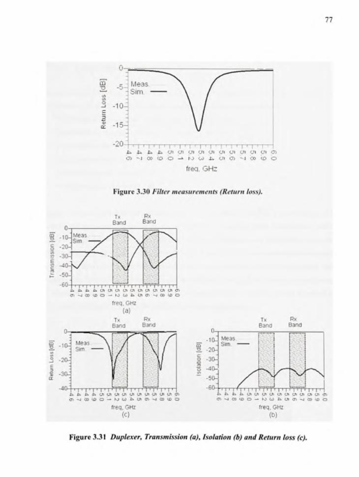
77
m
O
0) a:
CT)
I M ' I ' I • I ' I ' ! ' I ' I ' I ' ! x^ i^ i:. o^ (Si <j\ o i CJ l CJ l o i a i t n a i o - J 0 3 c o o - ^ r o c o j : ^ c J i c o - j c o c o o
freq, GHz
Figure 3.30 Filter measurements (Return loss).
CD • a
TO
CD
cr
, , , , I ' I ' I ' I . l i j ^ j ^ x ^ a i o i o i c n a i a i a i a i c j i o i u ^
C O C D C D — ' k 3 C 0 X : . b l C r ) ^ C 0 < J D O
freq, GHz (C)
•M I I n I M I M I I I I M I M M I I M . b . . b . i i i i C J i u i c n a i a i c j i c j i c r i a i a i c r ^ O I ^ J G O t i J C D — ' N J Q J X ^ C J l C T j ^ C O C i D O
freq, GHz (b)
Figure 3.31 Duplexer, Transmission (a). Isolation (b) and Return loss (c).

78
3.3.1.3 Secon d Fabrication Run
In the secon d fabricatio n m n w e have targeted a UMTS filter duplexer profile . Th e typica l
requirements for a UMTS filter duplexer for mobile terminals are as follows:
Pass Band for Transmission Filter : 1.92GH z to 1.98GHz
Pass Band for Recepfion Filter : 2.11 GHz to 2.170GHz
Tx-Antenna attenuation (Tx-band) <2
Rx- Antenna attenuation (Rx-band) <3
Tx-Rx isolation (Rx-band) >37
Tx-Rx isolation (Tx-band) >50
Figure 3.32 shows the fabricated transmi t and receiver filters for the UMST band, figure 3.3 3
presents th e measured result s fo r th e transmit filter an d compare s them t o simulatio n whil e
figure 3.3 4 present s a simila r compariso n betwee n simulatio n an d measuremen t fo r th e
receive filter. The fabricated duplexe r is shown in figure 3.35 and its measured and simulated
results ar e show n i n figur e 3.36 . Overall , ver y goo d agreemen t betwee n simulatio n an d
measurement i s observed fo r the filters and the duplexer. The slight differences ar e attributed
to som e effect s tha t ar e no t fiill y capture d b y electromagneti c simulation , suc h a s radiatio n
loss, metal thickness modeling and effect o f the measuring fixture .
I I I ! l i l l l l l l i I •i
l i l l l l l l i
Figure 3.32 UMTS filters topologies. (Left) Tx-filter (Right) Rx-filter
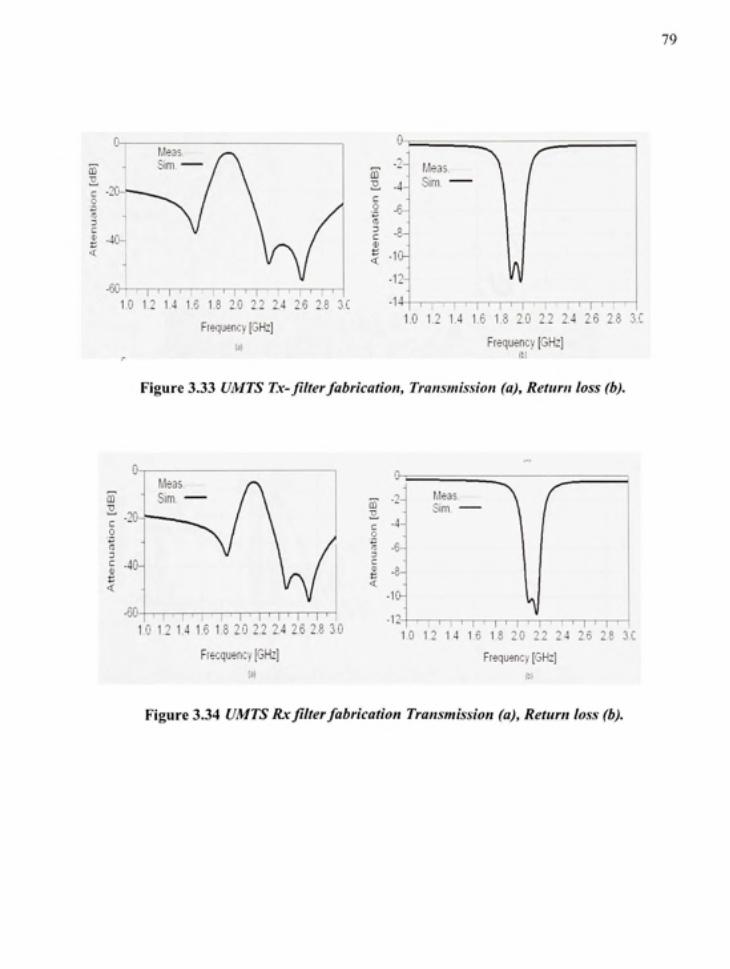
79
Meas, Sim. •
I ' I ' I ' ' I I I I • 1 ' I M 1.0 1. 2 1. 4 1. 6 1. 8 2. 0 2. 2 2. 4 2. 6 2. 8 3. C
Frequency [GHz]
(a)
a -4 -I -6 -CO
c c -
I -1C H -12-
-14-
Meas. Sim. -
• M M I ' I ' 1 ' I I 1.0 1. 2 1. 4 1. 6 1. 8 2. 0 2. 2 2. 4 2. 6 2 8 3. C
Frequency [GHz] (bi •
Figure 3.3 3 UMTS Tx- filter fabrication. Transmission (a). Return loss (b).
n — ^ ^ 1 — ' I M ' i ' I ' I 1.0 1. 2 1. 4 1. 6 1. 8 2. 0 2. 2 2 4 2. 6 2. 8 3. 0
Frecquency [GHz]
(a)
c o IZ 3 c 0)
<
0^
-2-
-4
-6-
-8-
-10H
-12
Meas. Sim. -
; ' 1 I I ' I I 1 I I ' ' I I ' I 1.0 1. 2 1. 4 1. 6 1 8 2 0 2. 2 2 4 2. 6 2. 8 3. C
Frequency [GHz]
lb)
Figure 3.3 4 UMTS Rx filter fabrication Transmission (a), Return loss (b).
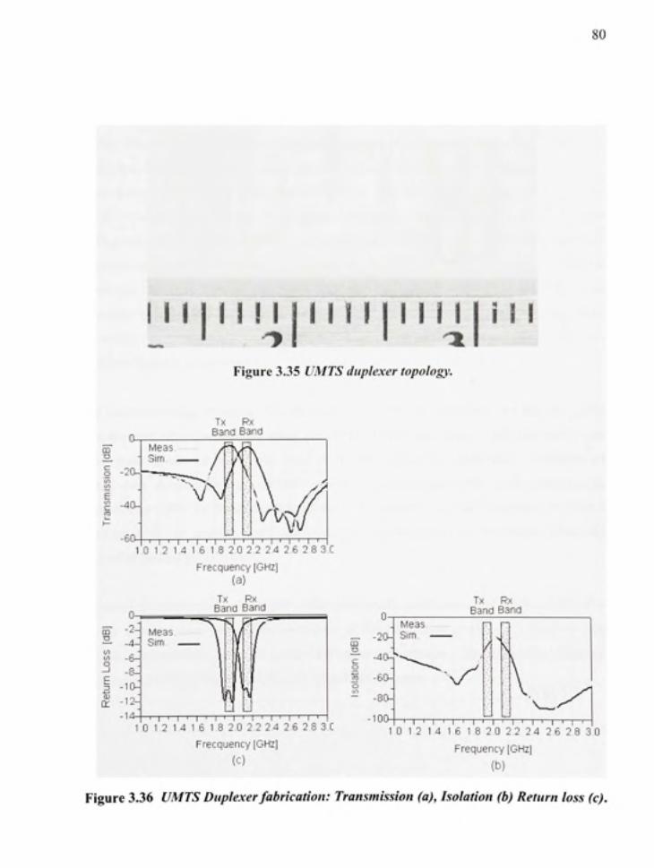
I I I I II ! I I 1I i I In il I i i i Figure 3.35 UMTS duplexer topology.
80
Tx R x B.3nd Ban d
CD
-2CU
-ao-
-60.
0-5- -2 -2- -4 -
I I I I I 1 I I I I I I I ' I ' I I 1.0 1. 2 1. 4 1 6 1. 8 2 0 2 2 2. 4 2. 6 2. 8 3.C
Frecquency [GHz ) (a)
Tx P x Band Ban d
Tx R x Band Ban d
o _ l c
QJ
- 6 -
-10--12--14
Meas. Sim
' I I I I ' I ! > I 1 0 1 2 1 4 1 6 1 8 2. 0 2 2 2 4 2 6 2 8 3 C
I ' i ' I ' I ' I I I I I I 1 ' I
1 0 1 2 1 4 1 6 1 8 2 0 2 2 2 4 2. 6 2 8 3 0 Frecquency [GHz ]
(c) Frequency [GHz ]
(b)
Figure 3.36 UMTS Duplexer fabrication: Transmission (a). Isolation (b) Return loss (c).

81
3.4 Conclusio n
In this chapte r w e hav e introduce d th e methodolog y develope d fo r designin g miniaturise d
filters and duplexers . W e hav e als o introduce d a new topolog y tha t provide s transmissio n
zeros abov e and below th e pass band o f the filter. Th e final stmcture highl y simplifie s th e
design o f thes e filters becaus e th e desig n parameter s ar e decouple d fro m al l bu t on e
performance metric . Th e proposed methodolog y fo r designing high qualit y filters using the
proposed stmctur e i s t o contro l th e bandwidt h o f th e filter usin g th e resonato r spacin g
parameter (X) , the n t o tun e th e positio n o f th e transmissio n zer o usin g th e offse t fee d
parameter (6 ) an d finall y t o adjus t th e retu m los s o f th e filter usin g th e fee d lin e widt h
parameter (Y) . Thi s techniqu e wa s show n t o produce s highl y compac t filters wit h ver y
attractive filtering characteristics.
The proposed design technique has been applied t o realise several filters and duplexers pairs
on a standard Alumin a substrate using an MHMIC fabrication process . Measuremen t result s
show goo d agreemen t wit h thos e obtaine d b y electromagneti c simulations . Althoug h th e
losses wer e elevate d fo r th e MHMI C process , i t wa s expecte d du e t o th e limite d meta l
thickness availabl e i n th e fabricafio n process . I n addition , th e hig h toleranc e (+/-5% ) i n
substrate thicknes s an d th e sensitivit y o f th e filter t o thi s paramete r resulte d i n a less tha n
optimal measured performance .
Although the results show significant miniaturization , the performance of the filters is limited
by th e Ohmi c losse s du e t o th e limitation s o f th e fabricatio n process . A mor e evolve d
process, such as MMIC process, could offe r bette r performance. Th e next chapte r discusse s
the development of filters and duplexers on a MMIC process.

CHAPTER 4
FILTERS AND DUPLEXERS IN MMIC TECHNOLOGY
4.1 Introduction
In the chapter we will present the design of miniaturised filter based on MMIC process. Th e
target process i s the TQPED process provided by TriQuint Semiconductors . Th e TQPED is
a pHEM T proces s o n whic h activ e component s an d hig h qualit y facto r passive s ca n b e
integrated. MMI C processe s ar e differen t fro m on e manufacture r t o anothe r bu t typica l
substrate parameters and stack-up are given in the Table 4.1.
Table 4.1
Typical stack up of a MMIC substrate
Layer
0
1
MO
ILDl
Ml
ILD2
M2
Material
Copper
GaAs
Aluminium
Insulator
Gold
Insulator
Gold
Function
Ground
Substrate
Metallization
Inter Layer
Dielectric 1
Metallization
Inter Layer
Dielectric2
Metallization
Thickness
(^m)
-254
0.4
1
2
3
4
Relative
Electric
Permittivity
-12.9
-2.8
-2.8
Electric
Conductivity
(S/m)
5.8e7
-2.9e7
4.1c7
4.1e7
Loss tangent
-0.0001
-
-
-
This proces s provide s bette r feature s fo r possibl e filter desig n suc h as , a hig h dielectri c
constant o f 12. 9 whic h i s goo d fo r hig h miniaturization , a highly precis e meta l depositio n
techniques, which allow s for les s spacing between feature s an d the possibility o f connectin g
all metal laye r together using stacked VIA s to obtain a metal thicknes s of as much as 6.4pm

83
leading to better unloaded qualit y factors . I n table 4.2 we note that the quarter wavelength of
the transmissio n lin e i s smalle r tha n tha t obtaine d fo r MHMI C substrat e o f tabl e 3.1 .
However, i t i s not clea r i f this wil l be sufficient t o realize very small-size distributed filters
and duplexers.
Table 4.2
Geometrical and electrical characteristics of a transmission line
Electrical
Characteristic
impedance Zo( fl )
Electrical length
(Deg.)
50
90°
Geometrical
Width (|a.m)
Length ( |am )
181
13100
4.2 Coupled resonator filter design
The procedure for designing the filter was introduced in previous chapters, consequently only
the mai n result s wil l b e presente d here . A filter fo r th e UMT S transmissio n ban d was
designed usin g a simplifie d stack-u p o f th e substrat e fo r th e purpos e o f spac e evaluation .
Figure 4. 1 show s th e topolog y o f th e designe d filter, whil e figur e 4. 2 present s th e
electromagnetic simulation results of this filter.
3.2mm
Figure 4.1 Preliminary coupled resonator filter on MMIC substrate.

84
CD p c: o CO
E CO c: H
n u
-10-
-20-_
-30--
-40--50-
- o u 1 II 1 1.6 1
1 1 1 1 ] 1 1
7 1. 8
/ ^
1 ? \ 1 f \
%^ h » \
• \ / '
1 1 1 1 1 1 1 ] 1 1 1 1 ] 1 1
1.9 2. 0 2. 1
Frequency. GH z
1 1 1 1 1
2.2
n
--5
_ -1 0
--15 ^
on 1 1 - i - w
2.3
Figure 4.2 Electromagnetic simulation results of geometry presented in Figure 4.1.
Electromagnetic simulatio n results presented i n figure 4.2 show very good attenuation in the
reception ban d an d relativel y goo d retu m loss , thes e ca n al l b e enhance d wit h fiirthe r
optimisation. Althoug h these preliminary simulation results are satisfactory i n themselves as
the siz e o f th e filter i s 0.17/ 1 xO.06/1 ^ which i s considerabl y miniaturised , bu t whe n
considered i n the context of the available space they fall short . Consequently , we considered
lumped element filter as a possible option for this technology.
4.3 Design of miniaturised lumped elements filte r
In view o f the limited spac e available an d the relatively larg e size of the coupled resonato r
filter, a different approac h was necessary to realise a miniaturised filter. A lumped elemen t
approach wa s chosen a s i t gives the maximum miniaturization . Althoug h th e design o f th e
filter is straightforward, th e complexity of the substrate and the fac t tha t stacke d via s do not
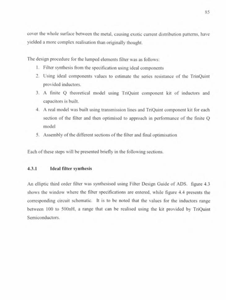
85
cover the whole surface between the metal, causing exotic current distribution pattems, have
yielded a more complex realisation than originally thought.
The design procedure for the lumped elements filter was as follows:
1. Filte r synthesis from the specificafion usin g ideal components
2. Usin g idea l component s value s t o estimat e th e serie s resistanc e o f th e TrinQuin t
provided inductors.
3. A finit e Q theoretica l mode l usin g TriQuin t componen t ki t o f inductor s an d
capacitors is built.
4. A real model was built using transmission line s and TriQuint componen t ki t for each
section o f th e filter and the n optimise d t o approac h i n performanc e o f th e finite Q
model
5. Assembl y of the different section s of the filter and final optimisation
Each of these steps will be presented briefly i n the following sections.
4.3.1 Idea l fdter synthesi s
An ellipti c thir d orde r filter was synthesise d usin g Filte r Desig n Guid e o f ADS . figur e 4. 3
shows th e window wher e th e filter specifications ar e entered , whil e figur e 4. 4 present s th e
corresponding circui t schematic . I t i s t o b e note d tha t th e value s fo r th e inductor s rang e
between 10 0 t o 500nH , a rang e tha t ca n b e realise d usin g th e ki t provide d b y TriQuin t
Semiconductors.
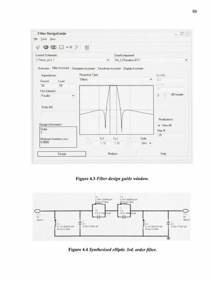
86
Fi l te r DesignGuid e
File Tool s Vie w
^ ^ ^ Q -- 0 ) < ^ j Current Schemati c
[ Thesis_pr | ] : 1
SmartComponent
DA_LCBandpassDT1
Overview Filte r Assistan t Simulatio n Assistant Sensitivit y Assistant Displa y Assistan t
Impedances
Source Loa d
|5Ci 5 0
First Elemen t
Parallel
Order (N )
Design Informatio n
Response Typ e
Elliptic
Order: 3
Minimum Insertio n Loss . 0 000 0
Design
Fpl h e s 1.9 2
Fp2
1.9S
Redraw
2.11
Ap (dB j
0.2
\
dB/square
Uinte_ TGHE
Realizations
•/ Vie w Al l
Max 8
25
Help
Figure 4.3 Filter design guide window.
O PI t*jm=1
L L2 1=381 72964 6 p H R=1e-12 0h m
L1 ' L=11 2 60516 7 p H
R=le-12 0h m
C2 C=16. l55l51 p F
• 0 1 0=59 17190 1 pF
L3 L=412 436829 p H R=le-12 0h m
C3 0=17 4 5 4 * 4 p F
L4 L=112 60516 7 p H R=1e-I2 0h m
<I> P2 r^m=2
•04 0=59.171901 p F
Figure 4.4 Synthesised elliptic 3rd. order filter.

87
4.3.2 Mode l with transmission lines
Two models hav e been constmcted : a model usin g transmission line s tha t ar e configured t o
map to the layers presented i n Table 4.1 and the components provided i n the TQPED design
kit. Anothe r mode l wa s constmcte d usin g onl y th e components o f the desig n kit , both ar e
illustrated i n figur e 4.5 . Th e mode l usin g transmissio n line s i s opfimise d t o approac h i n
performance tha t with only lumped components.
An interesting fact , tha t L I whos e value i s 112p H was too low an d no t realisabl e usin g the
inductors provide d i n the design kit . Thi s i s likely becaus e o f transmission lin e inductanc e
has large r influenc e tha n tha t o f th e lumpe d inductor . Thi s inducto r wa s realise d usin g a
short circuited transmission line as illustrated in figure 4.6.
Successively, eac h sectio n o f th e filter wa s optimise d i n a simila r fashio n unti l al l th e
sections were designed.
88
1 S-P>iRAWeTHRS
Slart=i7Q-e
aop=2 3G-C
3ep=
dudJ
Vpja)=0 lfeh=10 ^fln=^0 M5=10
l«w=10 ta j_g*3cw
Stall s6cd_Are(iSs=ai
StiBsOcdJrtcFOi
'U t i ' rOy^
£)«j^'ctoS(n)KtoS(3,3)r 9 fT(rBlancer«Te:^p r Mn=JD 00001 Nte(=0000O1
fen9eVai|lt=^trec|-R»igeMr(1f=^eQ-t tengeMti(1l=2 3 Q ^
GOAL
i j t r T t l H l O E>ti^c±jSi12)H±<S(3,4)C
Mn=0 00001
riAnFOOOom
RangeValipTTKl' FlangeMi1f=iea-6 Rargef*411=23Q-ft
S U E H
Er(1|=2e 1 11=3 2 i jn Tarq 11=0 0006 Tl11=4lTT, Ccnr 11=4 IE'7
E/[21^8 l-p)=1ifr> Tarq2)=00006 T[21=2t/n Ccnc<2)=dle7 Ej(;q=129 K3)=10 ml Taiq3|=OQ06 T13t=fl4ifT> Canfi]=26e*7
T14)Onil a>nt(d)=1 X * 50 La^Ti«( l )=6ig ia La^Typ^21=sgia L a ^ T i p ^ 3 ) ^ g d La^T>pe(4]=gard Lay«t^m^ 1 )=• qped_TvKA%• La,e^aneP]^^lT»Cl_Ole^«• La,«MaT f i tiTed_Ze»cMr LayerName(4]^'cHair La,«Waf.&fT^1Fttped_\^a2 L3,eVlaf feiTe(2Fttped_\^ a l' La,€fViaff i fTie^3Kl<»*d_Sii iVla-|_^^iQ^„3^
UBeajiQas=^CK
iybinefs=25 CesireeErcrOO StatL6Lp^=4 R fid Ard)6is-T fine"
Set9e5tvaues=>,eB
Sa€QafT«are=nD UtxMeCBtasa^-igs SaweiJomna^Tio S*ert I Herat ore ^x)
Sa»eCaien£F=no
T«TTl3
ri/TT^3 i t
!^
^ LVSJrt*^LVS_Va
Tsfnd
n/ti=4 Z=50Om
J V.C6 0 um X
-HZZl-
rifn=1 2=50 Om
U l SiiJEt=^StiBtr Lengh=60ijn
La,iw=1 R.GC_file=
Lffi^h=100 t/n
La*e=l R.GC_File= Fteuse«J3>no
5*1 !t=^Sil« r W1 VWVun
V J=W 1 u m L ,«= 1
112 ajbst=fSjfc6n-Lfin^h=50i/n
L3i«=1 R.a::_Rie=
FfeusrfajX=nD
T«ni2
I Z=50Oi n
71.12 Si±st='SaBtr Len^h=Ll l im
F4.GC_Rle=
Figure 4.5 Optimisation of a filter section including transmission lines Q model.
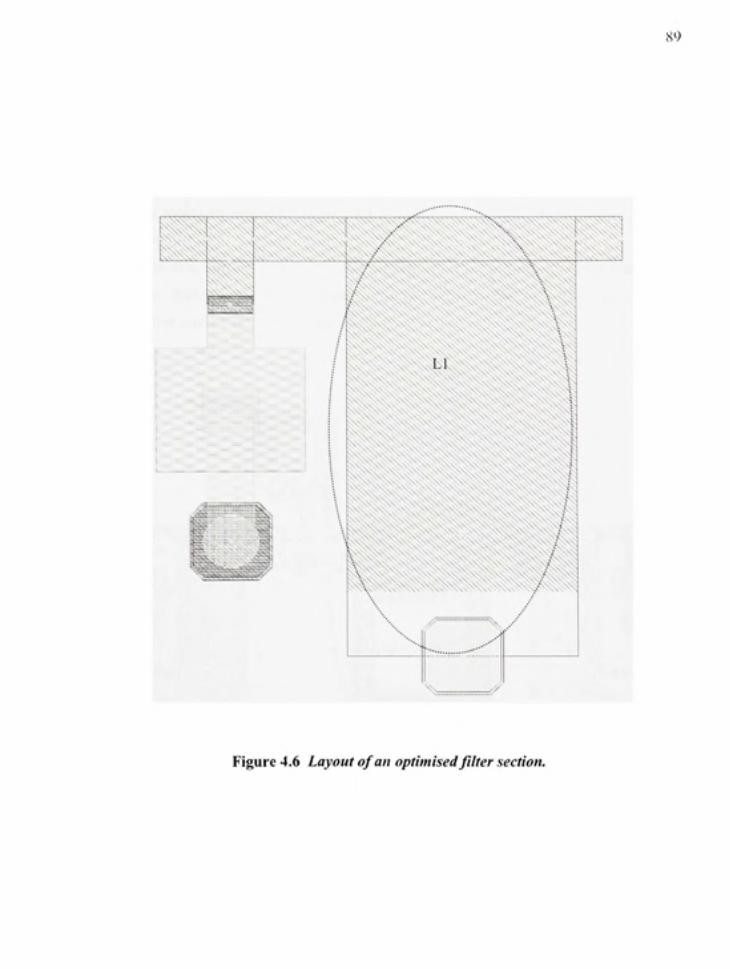
89
Figure 4.6 Layout of an optimised filter section.

90
4.3.3 Assembly and final optimisatio n
The filter section s wer e assemble d i n a single layou t the n circui t optimisatio n wa s use d t o
tune the circuit performance. A pair of UMTS filters were designed and their layout and the
simulation results are presented in figure 4.7 to figure 4.10
As we note from figures 4. 8 and 4.10 the insertion losse s are quite high. Thi s is mainly due
to th e lo w qualit y facto r o f th e inductors . A wa y t o overcom e thes e losse s i s t o us e Q -
compensated active inductors as suggested in [3].
Lower zero
Physical siz e
1.24mmX2mm
fc V . .:v'--
section
Figure 4.7 UMTS Tx band lumped element filter.

-10
m 7")
o if) fi)
E CO
-20-• • • *
^...1.
.,.-
-30 . -
-40 ~
••50^
Figure 4.8 UMTS Tx band lumped element filter - simulation results.
mmMm
Y^—I
Physical size
1.24mmX2mm
a
T ^
II II II II ^ \ ^ ; ~ ^ c : ^ ; ^ ^ x ^ ^ ^ § ;^?;^^^.-^;^;^^^^;<i^>^:^
Figure 4.9 UMTS Rx band filter.

92
freq. GHz
Figure 4.10 UMTS Rx band filter - simulation results.
4.4 Conclusion
In this chapte r w e have applie d th e topological optimisatio n techniqu e t o design a couple d
resonators filter o n a MMI C substrate . Th e result s o f th e simulation s sho w excellen t
performance an d miniaturisation fo r the distributed model . Whil e the filter is miniaturised in
size, it did not fit the space available for fabrication an d thus its fabrication was not pursued.
An altemativ e approac h wa s the n require d t o fiirther miniaturize th e filter. A filter usin g
lumped element s wa s the n designe d usin g th e desig n ki t provide d b y TrinQuin t
Semiconductor. Th e simulatio n result s sho w large r I L tha n it s couple d resonator s filter
counterpart. Losse s ar e mainl y du e t o lo w qualit y factor s o f inductors . O n th e
miniaturization fron t th e lumpe d element s filter i s orders o f magnitude smalle r tha n an y of
the couple d lin e resonator s filte r designed . However , give n it s limite d performanc e it s
fabrication wa s not pursued either .
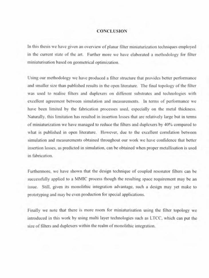
CONCLUSION
In this thesis we have given an overview of planar filter miniaturization techniques employed
in th e curren t stat e o f th e art . Furthe r mor e w e hav e elaborate d a methodology fo r filter
miniaturisation based on geometrical optimization .
Using our methodology w e have produced a filter stmcture that provides better performanc e
and smaller size than published result s in the open literature. Th e final topology of the filter
was use d t o realis e filters an d duplexer s o n differen t substrate s an d technologie s wit h
excellent agreemen t betwee n simulatio n an d measurements . I n term s o f performanc e w e
have bee n limite d b y th e fabricatio n processe s used , especiall y o n th e meta l thickness .
Naturally, thi s limitation has resulted i n insertion losse s that ar e relatively large but i n terms
of miniaturization w e have managed to reduce the filters and duplexers by 40% compared to
what i s publishe d i n ope n literature . However , du e t o th e excellen t correlatio n betwee n
simulation an d measurements obtaine d throughou t ou r wor k w e have confidenc e tha t bette r
insertion losses, as predicted in simulation, can be obtained when proper metallisation i s used
in fabrication .
Furthermore, w e hav e show n tha t th e desig n techniqu e o f couple d resonato r filters ca n b e
successfully applie d t o a MMIC process thoug h th e resulting spac e requirement ma y be an
issue. Still , give n it s monolithi c integratio n advantage , suc h a desig n ma y ye t mak e t o
prototyping and may be even production for special applications.
Finally w e not e tha t ther e i s mor e roo m fo r miniaturisatio n usin g th e fflte r topolog y w e
introduced i n this work by using multi laye r technologies suc h a s LTCC, which ca n put the
size of filters and duplexers within the realm of monolithic integration.
BIBLIOGRAPHY
[ 1 ] Aigner , R. , Integration of Bulk Acoustic Wave Filters: Concepts and Trends, i n MTT-S Digest. 2004 .
[2] Hien g Tiong, S. , F . Huang, and M.J . Lancaster , Highly miniature HTS microwave filters. Applie d Superconductivity , IEE E Transactions on , 2001. 11(1): p. 349-352.
[3] Kuhn , W.B. , F.W. Stephenson , an d A. Elshabini-Riad , A 200 MHz CMOS Q-enhanced LC bandpass filter. Solid-Stat e Circuits, IEEE Journal o f 1996 . 31(8): p. 1112-1122 .
[4] Sagawa , M. , K. Takahashi, an d M. Makimoto, Miniaturized hairpin resonator filters and their application to receiver front-end MICs. Microwav e Theory an d Techniques , IEEE Transactions on , 1989 . 37(12): p. 1991-1997 .
[5] Sheng-Yuan , L . and T . Chih-Ming, New cross-coupled filter design using improved hairpin resonators. Microwav e Theory an d Techniques , IEE E Transactions on , 2000 . 48(12): p. 2482-2490.
[6] Chi-Feng , C , e t al. , A miniaturized multilayer quasi-elliptic bandpass filter with aperture-coupled microstrip resonators. Microwav e Theory an d Techniques , IEE E Transactions on , 2005. 53(9): p. 2688-2692.
[7] Hong , J.S. and M.J . Lancaster , Microstrip filters for RF/microwave applications. Wiley series in microwave an d optical engineering . 2001 , New York : Wiley , xii , 471 P-
[8] Goron , E. , et al . Accessing to UMTS filtering specifications using new microstrip miniaturized loop-filters, i n Microwave Symposium Digest. 2003 IEEE MTT-S International. 2003 .
[9] Cohn , S.B. , Direct-Coupled-Resonator Filters. Proceeding s o f the IRE , 1957 . 45(2): p. 187-196.
[10] Cohn , S.B. , Parallel-Coupled Transmission-Line-Resonator Filters. Microwav e Theory and Techniques , IEE E Transacfions on , 1958 . 6(2) : p. 223-231 .
95
[11] Dishal , M. , Alignment and Adjustment of Synchronously Tuned Multiple-Resonant-Circuit Filters. Proceeding s o f the IRE , 1951 . 39(11): p. 1448-1455 .
[12] Rizzi , P.A. , Microwave engineering : passive circuits. 1988 , Englewood Cliffs , N.J . Prentice Hall , xvi , 572 p.
[13] Matthaei , G.L. , Microwave filters : impedance-matching networks, and coupling structures. 1964 , New York: McGraw-Hill , xv , 109 6 p.
[14] AgilentTechnologies , ADS2004A User Manual. 2005 .
[ 15] Levy , R. , Filters with Single Transmission Zeros at Real or Imaginaiy Frequencies. Microwave Theory an d Techniques , IEEE Transacfions on , 1976 . 24(4): p. 172-181 .
[16] Hosoya , K. , et al . A low phase-noise 38-GHz HBT MMIC oscillator utilizing a novel transmission line resonator, i n Microwave Symposium Digest., 2000 IEEE MTT-S International. 2000 .
[17] Amari , S. , e t al . New parallel /spl lambda//2-microstrip line filters with transmission zeros at finite frequencies, i n Microwave Symposium Digest, 2003 IEEE MTT-S International. 2003 .
[18] Woodin , C . C . Woodin, and M . Goff Verification of MMIC on-wafer microstrip TRL calibrationVerifiication of MMIC on-wafer microstrip TRL calibration, i n Microwave Symposium Digest, 1990., IEEE MTT-S International. 1990 .
[19] Puglia , K.K. , A general design procedure for bandpass filters dirieved from low pass prototype elements. Microwav e joumal, 2001.