ece 546 lecture 12 integrated circuitsemlab.illinois.edu/ece546/lect_12.pdflecture 12 integrated...
TRANSCRIPT
ECE 546 – Jose Schutt‐Aine 1
ECE 546Lecture 12
Integrated CircuitsSpring 2020
Jose E. Schutt-AineElectrical & Computer Engineering
University of [email protected]
ECE 546 – Jose Schutt‐Aine 2
Integrated Circuits
• IC Requirements– Biasing of ICs is based on the use of constant
current sources– Use current mirrors– Source circuits are used as loads
ECE 546 – Jose Schutt‐Aine 3
• Analog Design Requirements– Analog ICs may need resistors and capacitors for
the design of amplifiers– Resistors and capacitors occupy the space of
tens or hundreds of MOS devices– It is important to minimize their use
Integrated Circuits
ECE 546 – Jose Schutt‐Aine 4
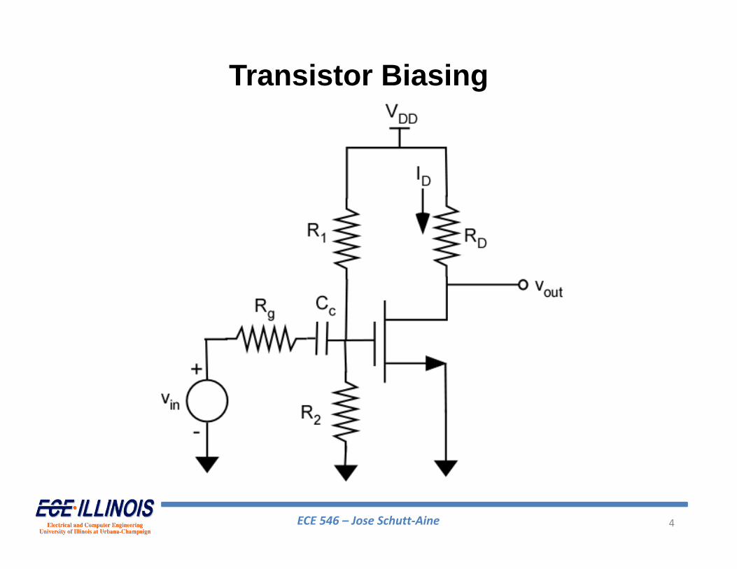
Transistor Biasing
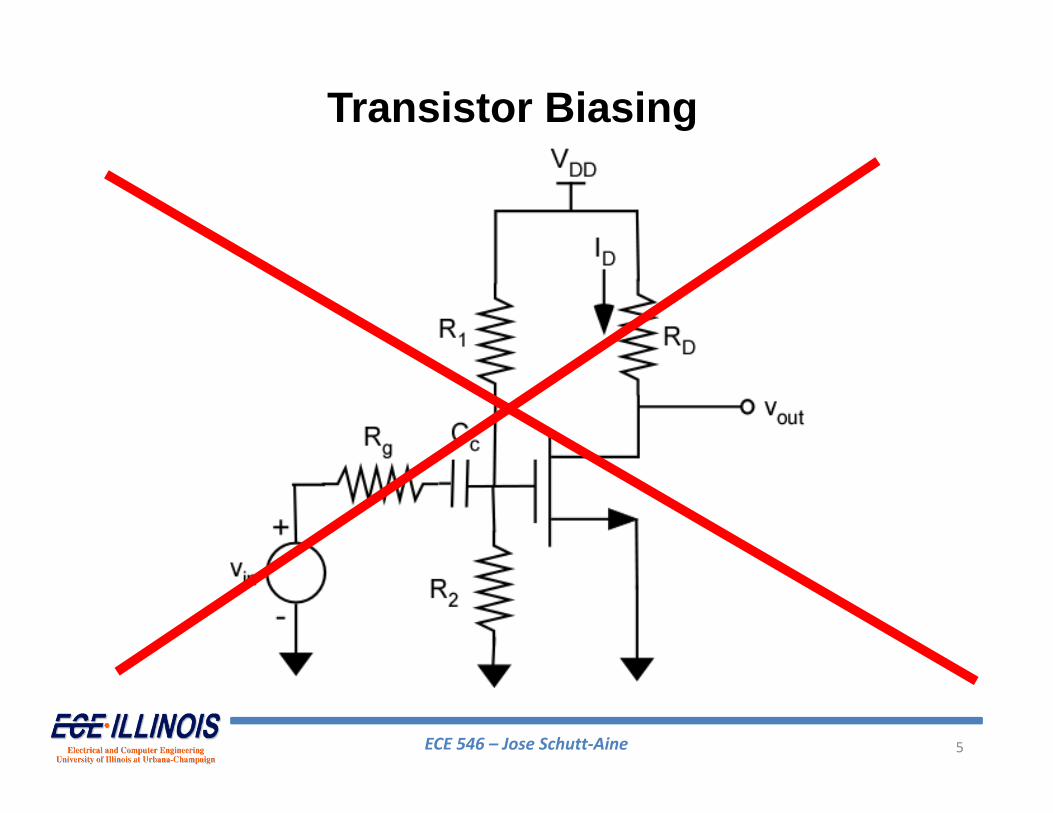
ECE 546 – Jose Schutt‐Aine 5
Transistor Biasing
ECE 546 – Jose Schutt‐Aine 6
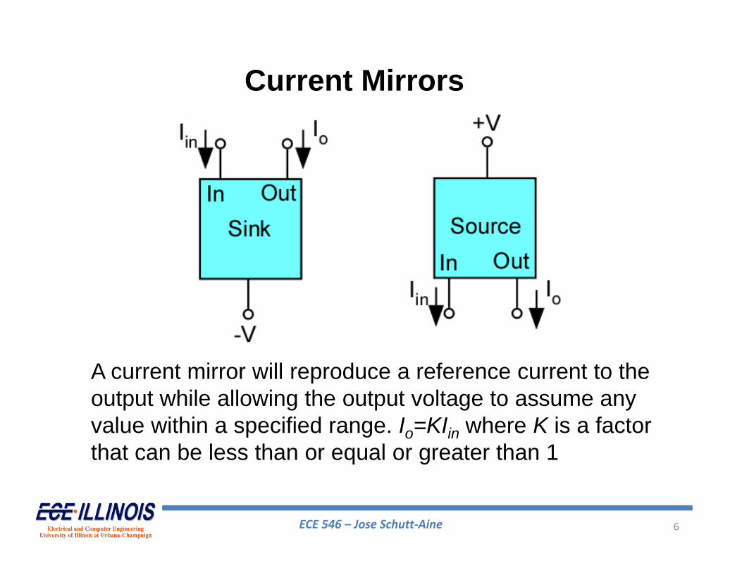
Current Mirrors
A current mirror will reproduce a reference current to the output while allowing the output voltage to assume any value within a specified range. Io=KIin where K is a factor that can be less than or equal or greater than 1
ECE 546 – Jose Schutt‐Aine 7
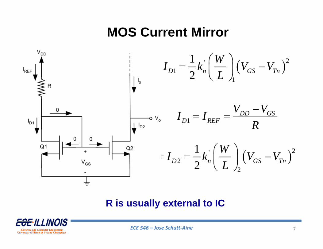
MOS Current Mirror
2'1
1
12D n GS Tn
WI k V VL
1DD GS
D REFV VI I
R
2'2
2
12o D n GS Tn
WI I k V VL
R is usually external to IC
ECE 546 – Jose Schutt‐Aine 8
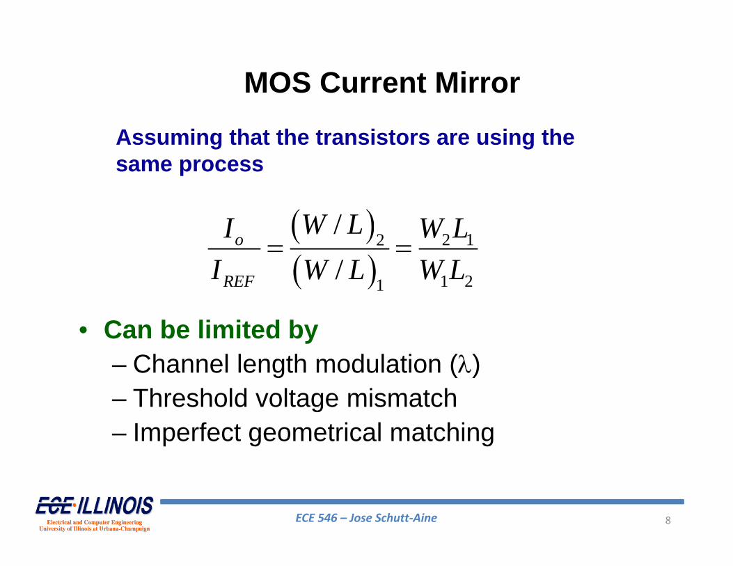
MOS Current Mirror
2 12
1 21
//
o
REF
W LI W LI W L W L
Assuming that the transistors are using the same process
• Can be limited by– Channel length modulation ()– Threshold voltage mismatch– Imperfect geometrical matching
ECE 546 – Jose Schutt‐Aine 9
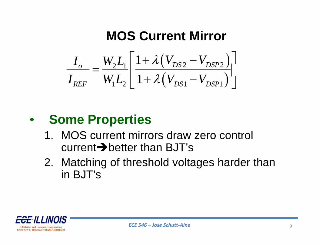
MOS Current Mirror
2 22 1
1 2 1 1
11
DS DSPo
REF DS DSP
V VI W LI W L V V
• Some Properties1. MOS current mirrors draw zero control
currentbetter than BJT’s2. Matching of threshold voltages harder than
in BJT’s
ECE 546 – Jose Schutt‐Aine 10
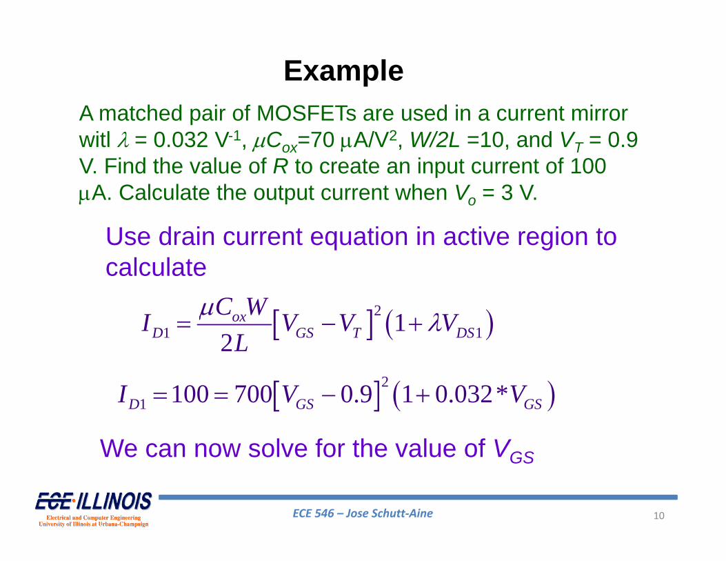
ExampleA matched pair of MOSFETs are used in a current mirror witl = 0.032 V-1, Cox=70 A/V2, W/2L =10, and VT = 0.9 V. Find the value of R to create an input current of 100 A. Calculate the output current when Vo = 3 V.
21 11
2ox
D GS T DSC WI V V V
L
Use drain current equation in active region to calculate
21 100 700 0.9 1 0.032*D GS GSI V V
We can now solve for the value of VGS
ECE 546 – Jose Schutt‐Aine 11
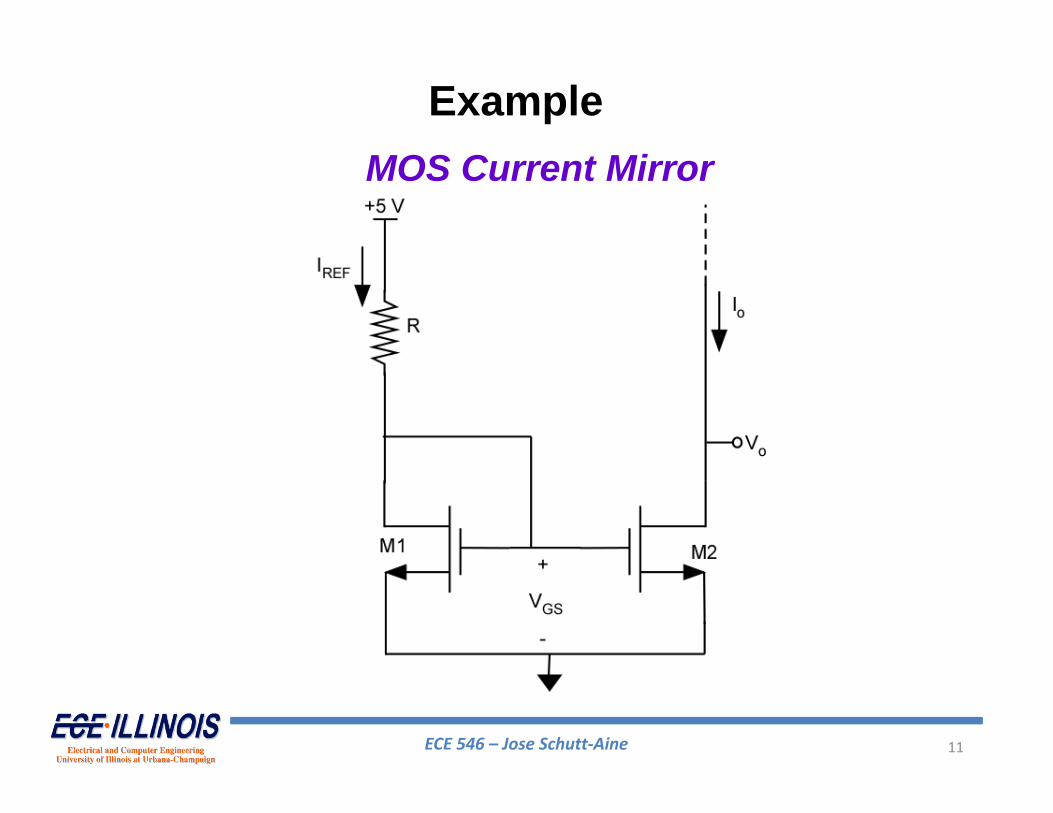
ExampleMOS Current Mirror
ECE 546 – Jose Schutt‐Aine 12
Example
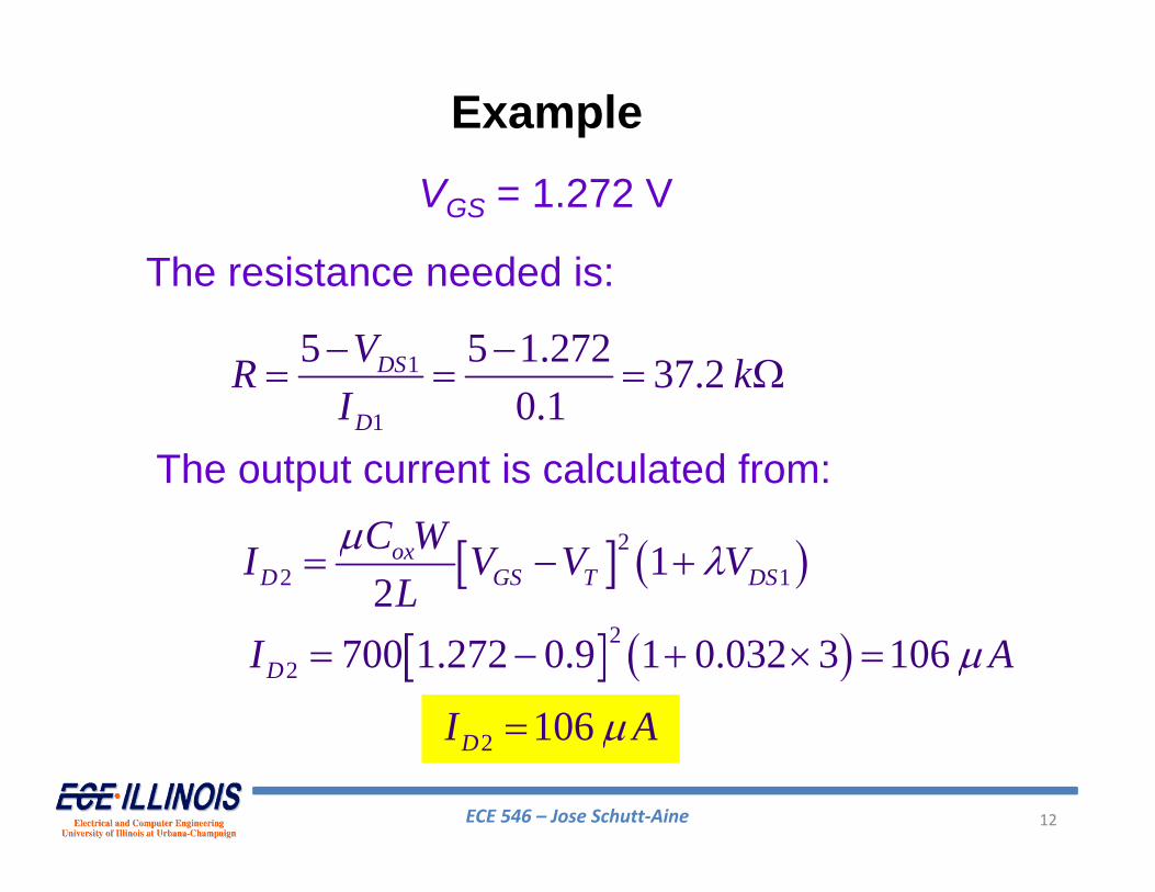
1
1
5 5 1.272 37.20.1
DS
D
VR kI
The resistance needed is:
The output current is calculated from:
22 700 1.272 0.9 1 0.032 3 106DI A
VGS = 1.272 V
2 106DI A
22 11
2ox
D GS T DSC WI V V V
L
ECE 546 – Jose Schutt‐Aine 13
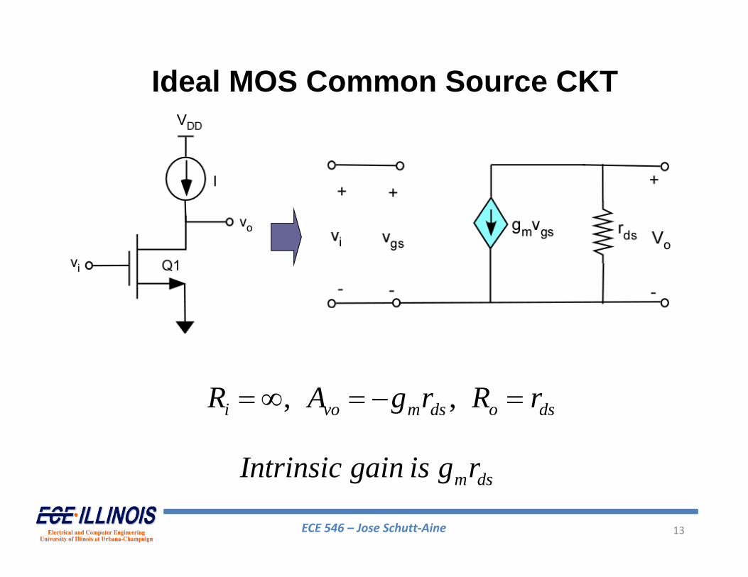
Ideal MOS Common Source CKT
, ,i vo m ds o dsR A g r R r
m dsIntrinsic gain is g r
ECE 546 – Jose Schutt‐Aine 14
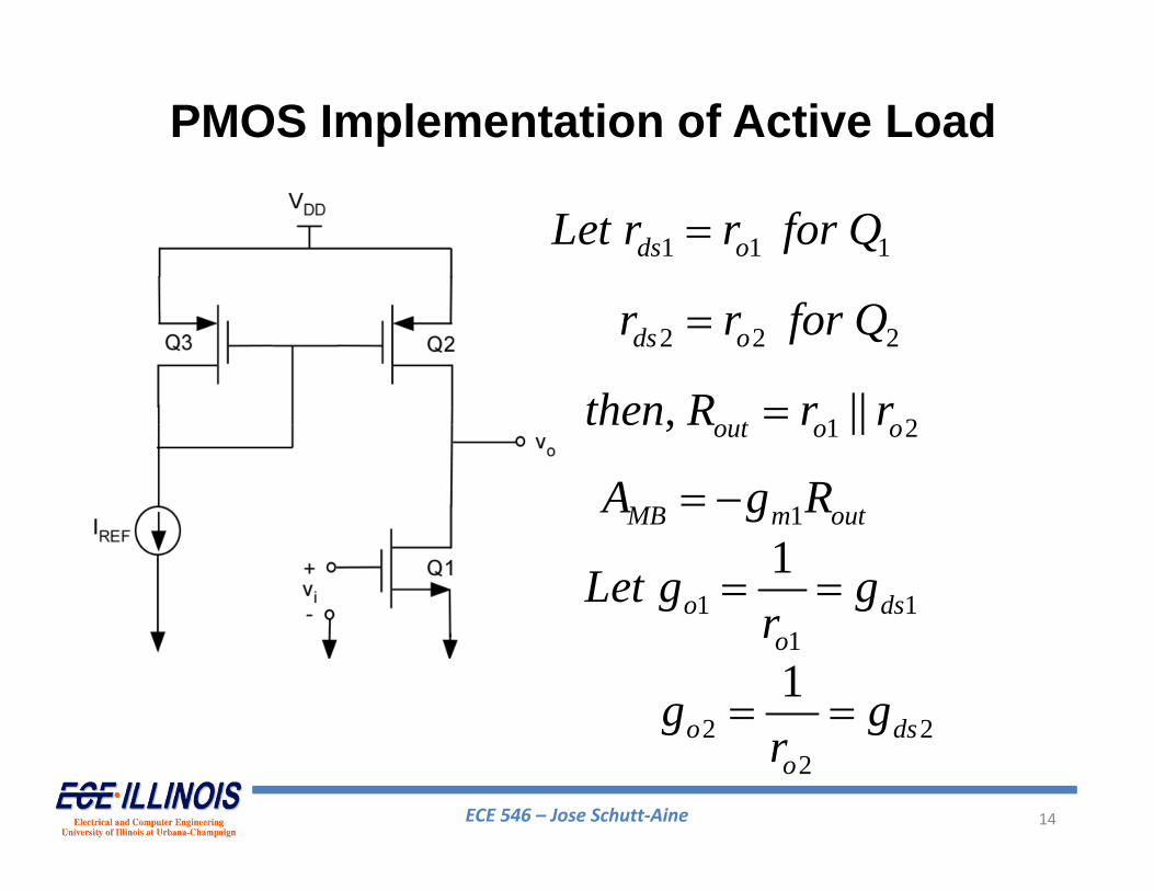
PMOS Implementation of Active Load
1 1 1ds oLet r r for Q
2 2 2ds or r for Q
1 2, ||out o othen R r r
1MB m outA g R
1 11
1o ds
o
Let g gr
2 22
1o ds
o
g gr
ECE 546 – Jose Schutt‐Aine 15
PMOS Implementation of Active Load
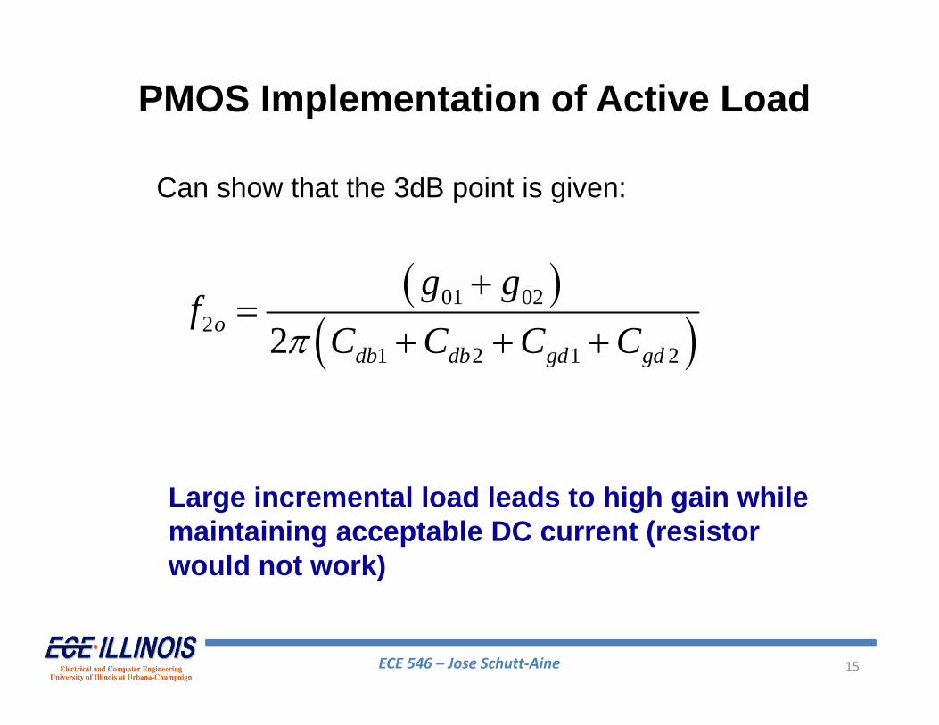
01 022
1 2 1 22odb db gd gd
g gf
C C C C
Can show that the 3dB point is given:
Large incremental load leads to high gain while maintaining acceptable DC current (resistor would not work)
ECE 546 – Jose Schutt‐Aine 16
Background• Differential Amplifiers
– The input stage of every op amp is a differential amplifier
– Immunity to temperature effects– Ability to amplify dc signals– Well-suited for IC fabrication because
– (a) they depend on matching of elements– (b) they use more components
– Less sensitive to noise and interference– Enable to bias amplifier and connect to other
stage without the use of coupling capacitors
ECE 546 – Jose Schutt‐Aine 17
Differential Amplifiers
• Practical Considerations– Both inputs to a differential amplifier may have
different voltages applied to them– In the ideal situation with perfectly symmetric
stages, the common-mode input would lead to zero output
– Temperature drifts in each stage are often common-mode signals
– Power supply noise is a common-mode signal and has little effect on the output signal
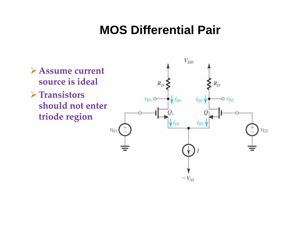
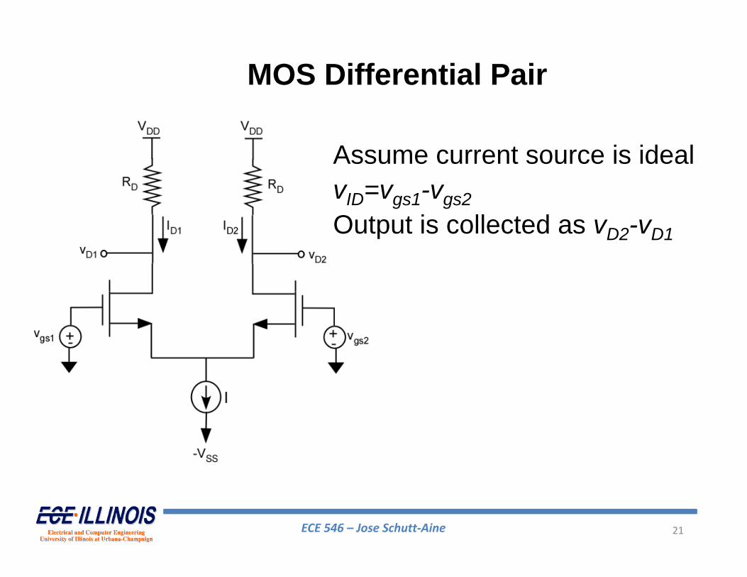
MOS Differential Pair
Assume current source is ideal
Transistors should not enter triode region
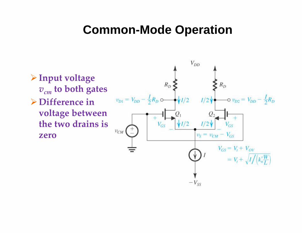
Common-Mode Operation
Input voltage vcm to both gates
Difference in voltage between the two drains is zero
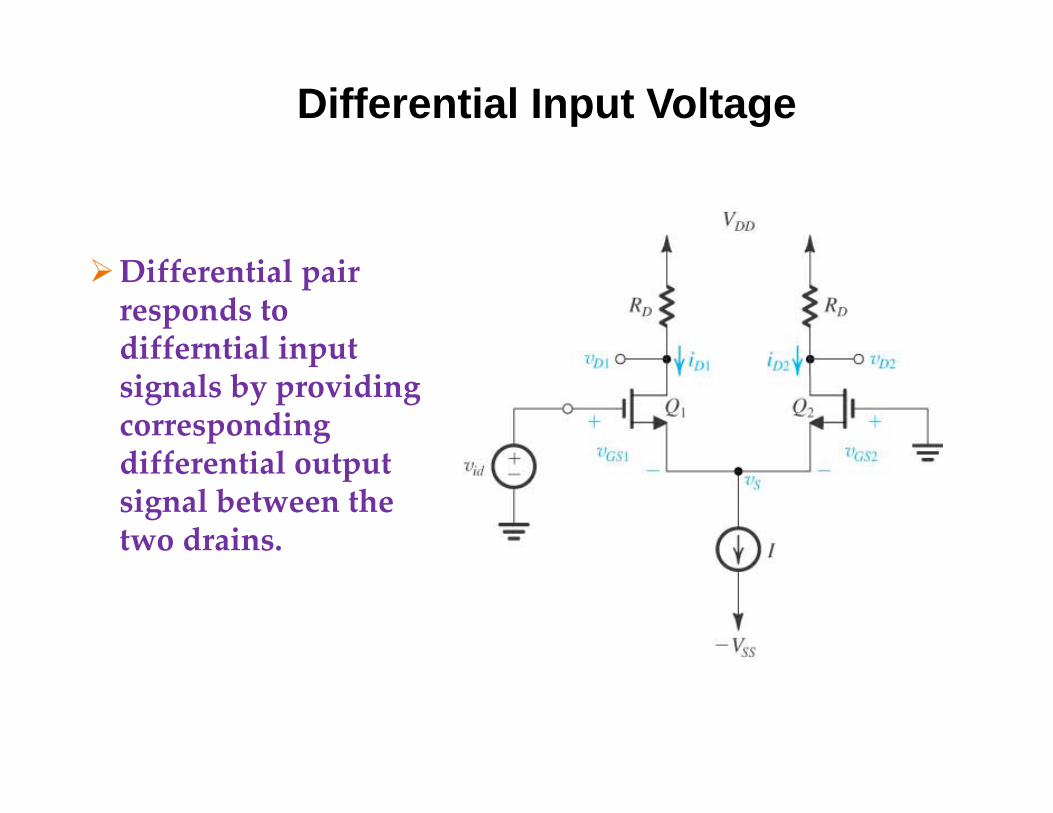
Differential Input Voltage
Differential pair responds to differntial input signals by providing corresponding differential output signal between the two drains.
ECE 546 – Jose Schutt‐Aine 21
MOS Differential Pair
Assume current source is idealvID=vgs1-vgs2Output is collected as vD2-vD1
ECE 546 – Jose Schutt‐Aine 22
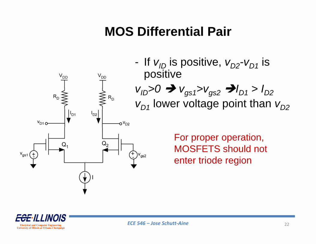
- If vID is positive, vD2-vD1 is positive
vID>0 vgs1>vgs2 ID1 > ID2vD1 lower voltage point than vD2
MOS Differential Pair
For proper operation, MOSFETS should not enter triode region
ECE 546 – Jose Schutt‐Aine 23
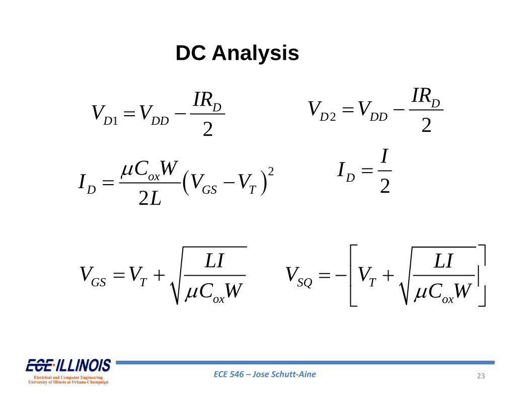
DC Analysis
1 2D
D DDIRV V 2 2
DD DD
IRV V
2
2ox
D GS TC WI V V
L
2DII
GS Tox
LIV VC W
SQ Tox
LIV VC W
ECE 546 – Jose Schutt‐Aine 24
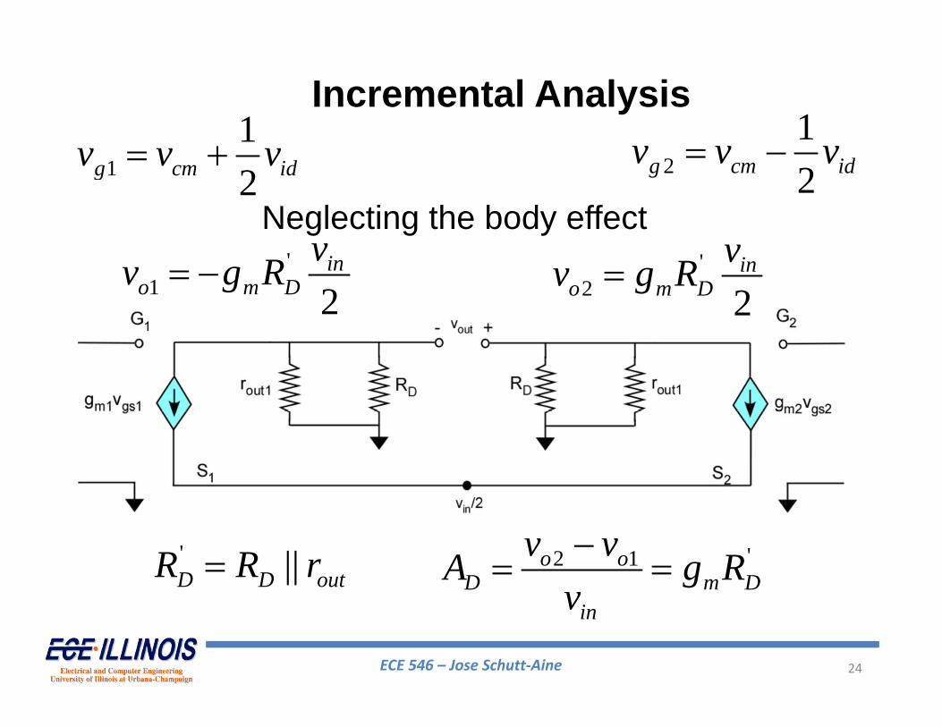
Incremental Analysis
'1 2
ino m D
vv g R Neglecting the body effect
'2 2
ino m D
vv g R
' ||D D outR R r '2 1o oD m D
in
v vA g Rv
112
g cm idv v v 212
g cm idv v v
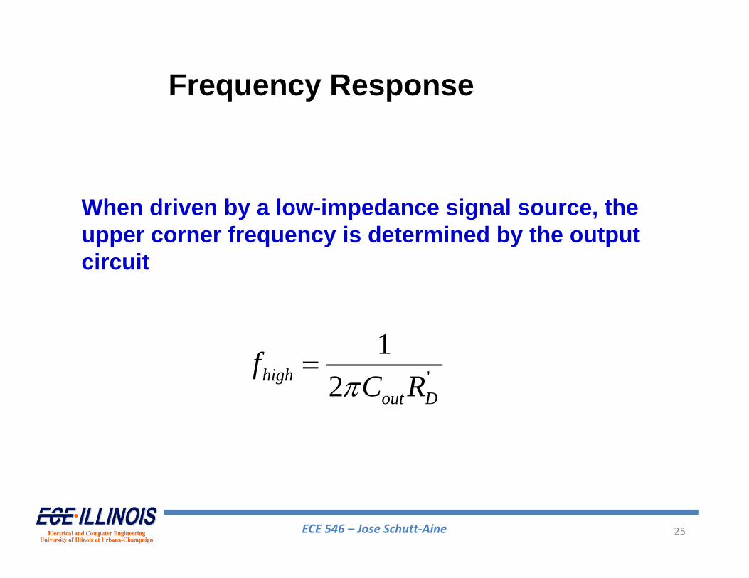
ECE 546 – Jose Schutt‐Aine 25
'
12high
out D
fC R
Frequency Response
When driven by a low-impedance signal source, the upper corner frequency is determined by the output circuit
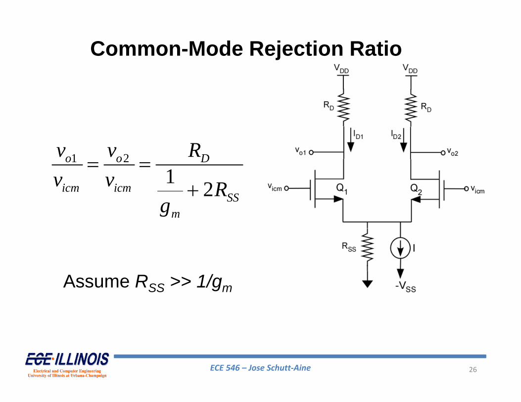
ECE 546 – Jose Schutt‐Aine 26
1 2
1 2o o D
icm icmSS
m
v v Rv v R
g
Assume RSS >> 1/gm
Common-Mode Rejection Ratio
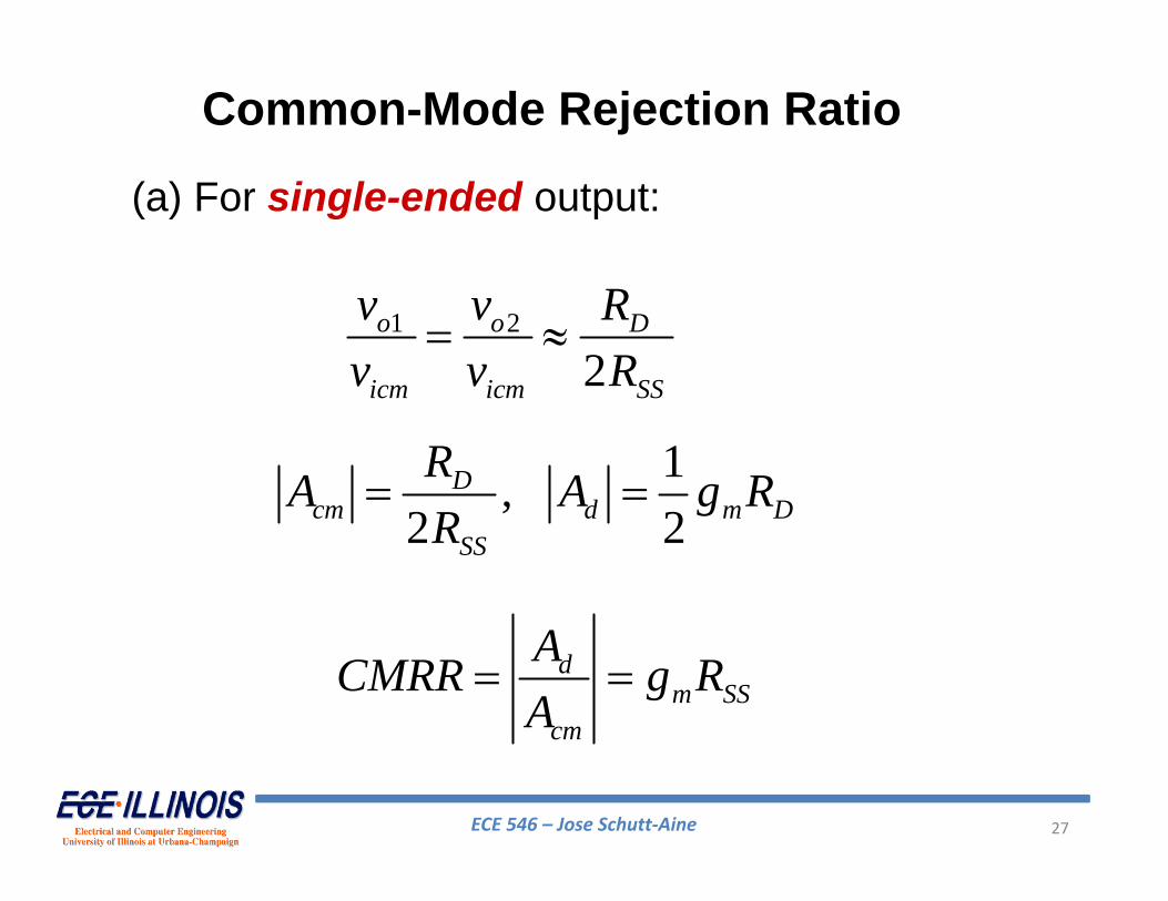
ECE 546 – Jose Schutt‐Aine 27
1 2
2o o D
icm icm SS
v v Rv v R
1,2 2
Dcm d m D
SS
RA A g RR
(a) For single-ended output:
dm SS
cm
ACMRR g RA
Common-Mode Rejection Ratio
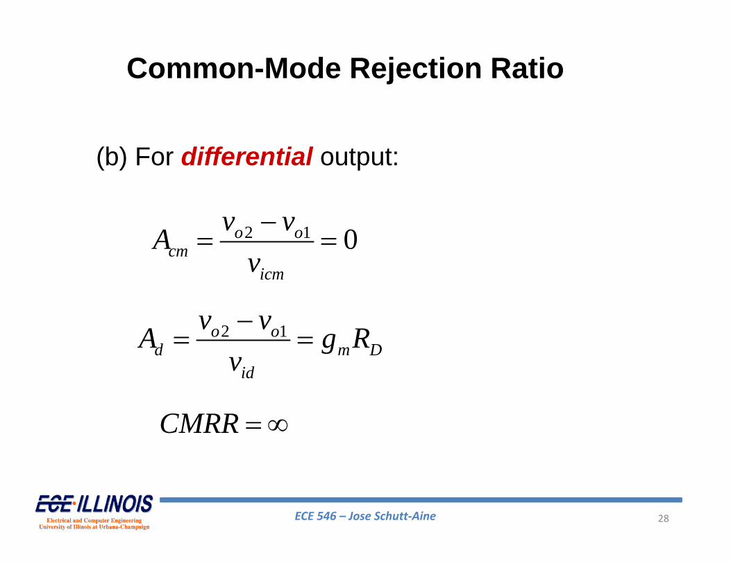
ECE 546 – Jose Schutt‐Aine 28
Common-Mode Rejection Ratio
(b) For differential output:
2 1 0o ocm
icm
v vAv
2 1o od m D
id
v vA g Rv
CMRR
ECE 546 – Jose Schutt‐Aine 29
Differential Amplifiers - Observations
• Observations– The differential pair attenuates the input signal of
each stage by a factor of one-half cutting the gain of each stage by one-half
– The double-ended output causes the two single-ended gains to be additive
– Thus, the voltage gain of a perfectly matched differential stage is equal to that of a single stage
ECE 546 – Jose Schutt‐Aine 30
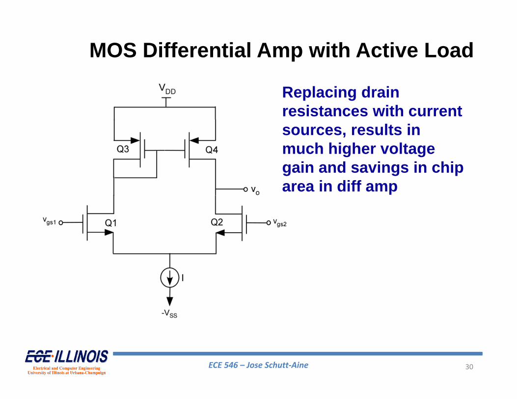
Replacing drain resistances with current sources, results in much higher voltage gain and savings in chip area in diff amp
MOS Differential Amp with Active Load
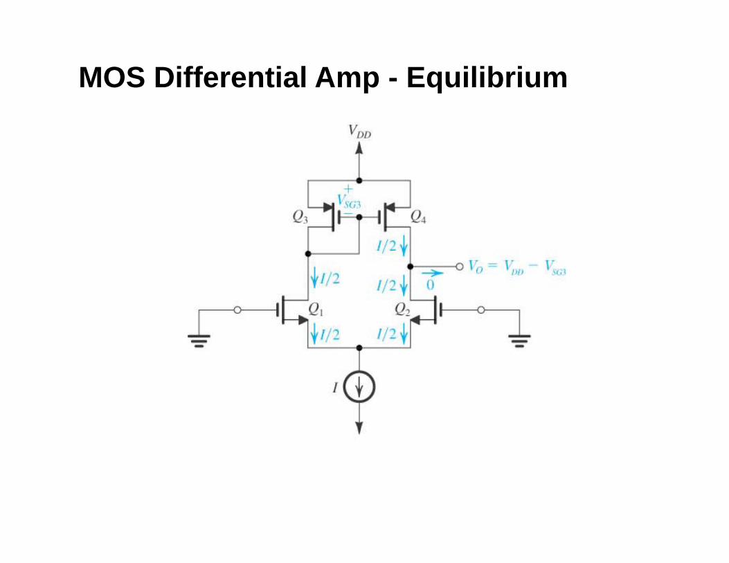
MOS Differential Amp - Equilibrium
ECE 546 – Jose Schutt‐Aine 32
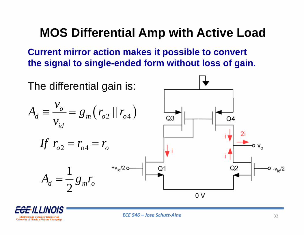
Current mirror action makes it possible to convert the signal to single-ended form without loss of gain.
MOS Differential Amp with Active Load
2 4||od m o o
id
vA g r rv
2 4o o oIf r r r
12d m oA g r
The differential gain is:
ECE 546 – Jose Schutt‐Aine 33
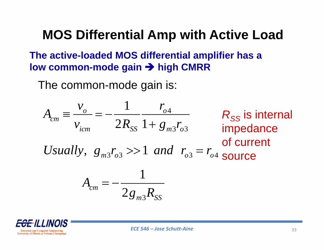
The active-loaded MOS differential amplifier has a low common-mode gain high CMRR
MOS Differential Amp with Active Load
4
3 3
12 1
o ocm
icm SS m o
v rAv R g r
3 3 3 4, 1m o o oUsually g r and r r
The common-mode gain is:
3
12cm
m SS
Ag R
RSS is internal impedanceof current source
ECE 546 – Jose Schutt‐Aine 34
MOS Differential Amp with Active Load
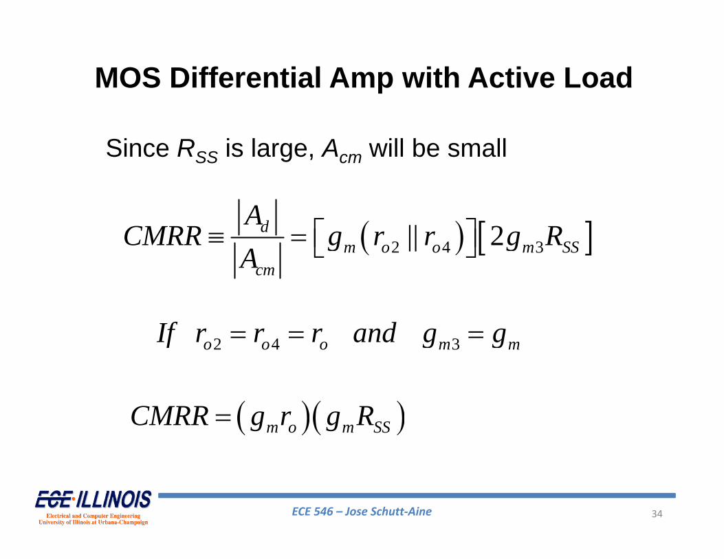
2 4 3|| 2dm o o m SS
cm
ACMRR g r r g R
A
Since RSS is large, Acm will be small
2 4 3o o o m mIf r r r and g g
m o m SSCMRR g r g R
ECE 546 – Jose Schutt‐Aine 35
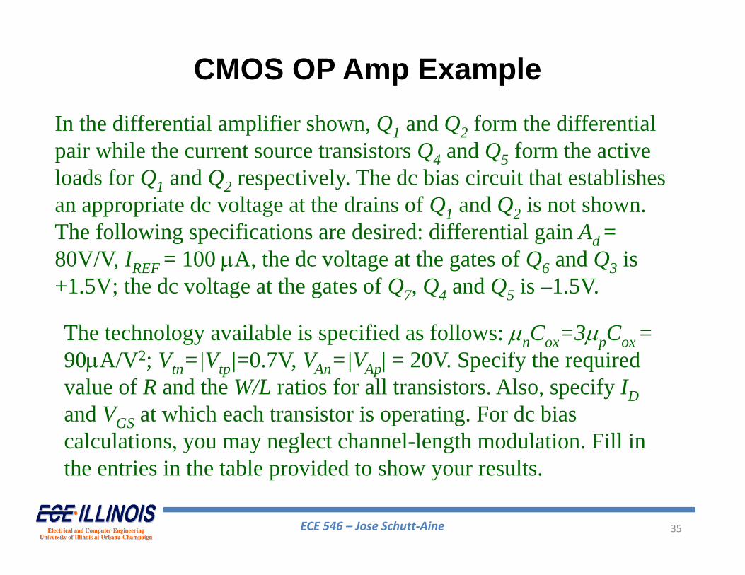
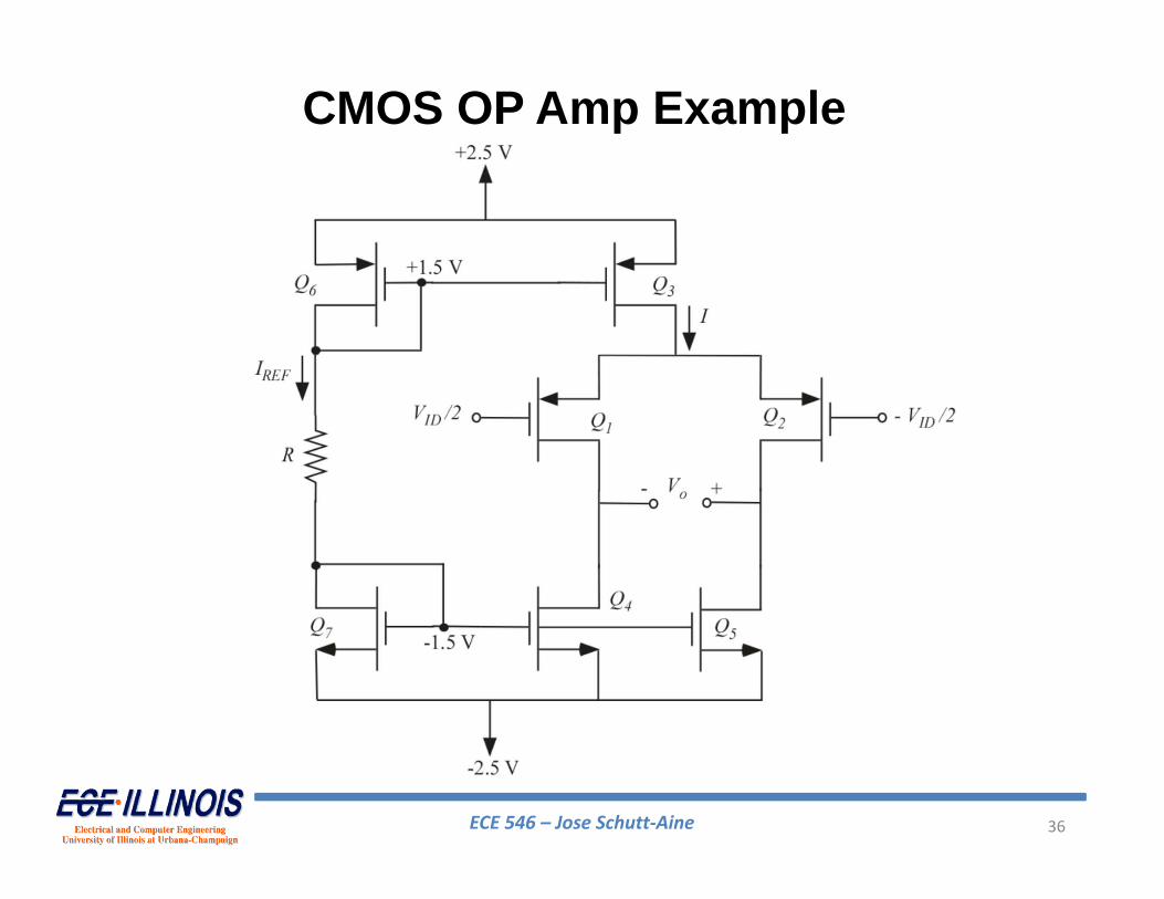
In the differential amplifier shown, Q1 and Q2 form the differential pair while the current source transistors Q4 and Q5 form the active loads for Q1 and Q2 respectively. The dc bias circuit that establishes an appropriate dc voltage at the drains of Q1 and Q2 is not shown. The following specifications are desired: differential gain Ad = 80V/V, IREF = 100 A, the dc voltage at the gates of Q6 and Q3 is +1.5V; the dc voltage at the gates of Q7, Q4 and Q5 is –1.5V.
CMOS OP Amp Example
The technology available is specified as follows: nCox=3pCox = 90A/V2; Vtn=|Vtp|=0.7V, VAn=|VAp| = 20V. Specify the required value of R and the W/L ratios for all transistors. Also, specify IDand VGS at which each transistor is operating. For dc bias calculations, you may neglect channel-length modulation. Fill in the entries in the table provided to show your results.
ECE 546 – Jose Schutt‐Aine 36
CMOS OP Amp Example
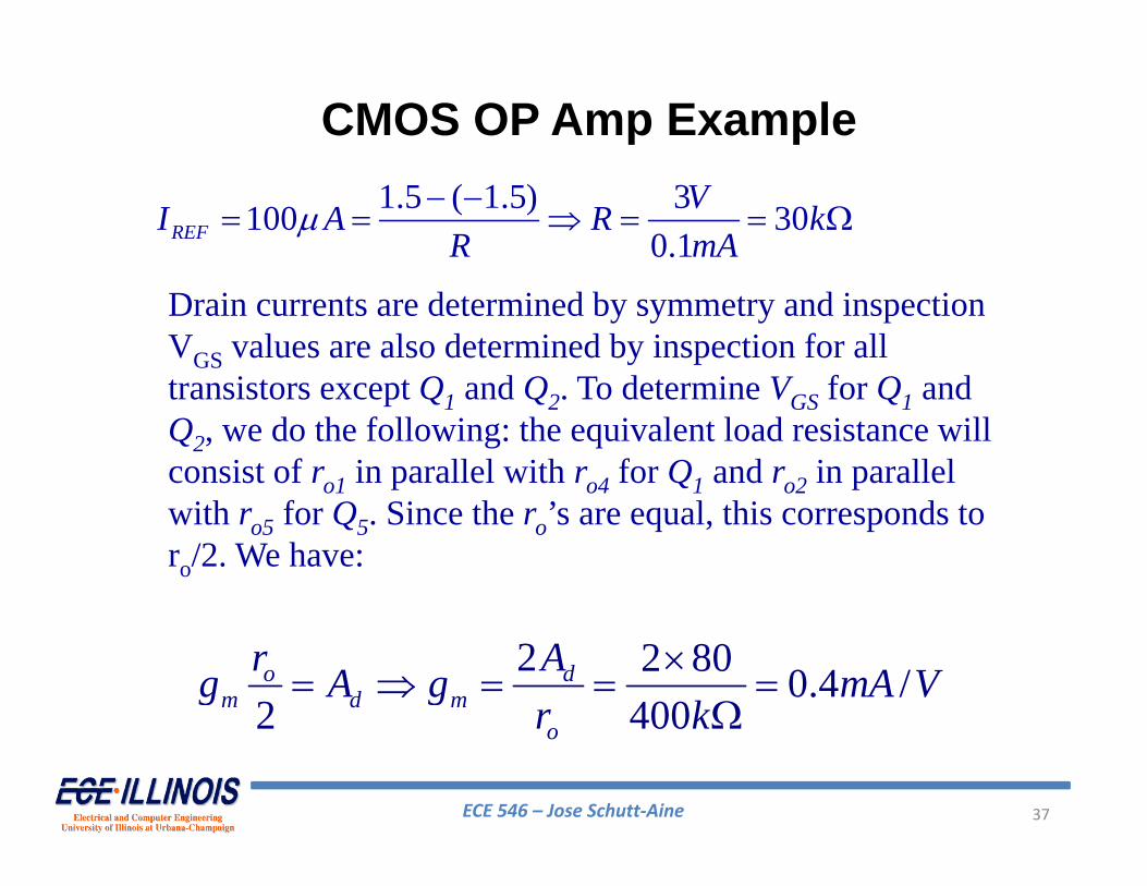
ECE 546 – Jose Schutt‐Aine 37
1.5 ( 1.5) 3100 300.1REF
VI A R kR mA
Drain currents are determined by symmetry and inspectionVGS values are also determined by inspection for all transistors except Q1 and Q2. To determine VGS for Q1 and Q2, we do the following: the equivalent load resistance will consist of ro1 in parallel with ro4 for Q1 and ro2 in parallel with ro5 for Q5. Since the ro’s are equal, this corresponds to ro/2. We have:
2 2 80 0.4 /2 400o d
m d mo
r Ag A g mA Vr k
CMOS OP Amp Example
ECE 546 – Jose Schutt‐Aine 38
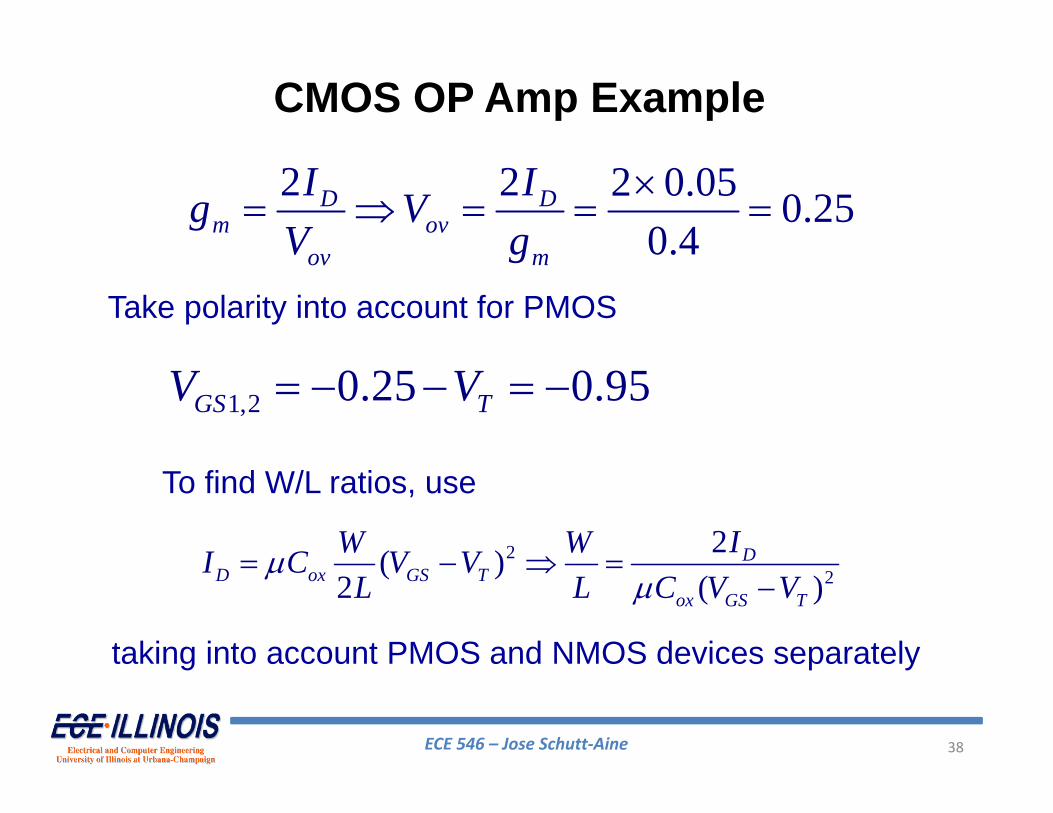
Take polarity into account for PMOS
1,2 0.25 0.95GS TV V
To find W/L ratios, use
22
2( )2 ( )
DD ox GS T
ox GS T
IW WI C V VL L C V V
taking into account PMOS and NMOS devices separately
2 2 2 0.05 0.250.4
D Dm ov
ov m
I Ig VV g
CMOS OP Amp Example
ECE 546 – Jose Schutt‐Aine 39
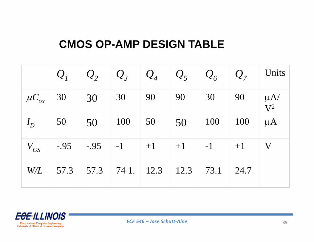
Q1 Q2 Q3 Q4 Q5 Q6 Q7 Units
Cox 30 30 30 90 90 30 90 A/V2
ID 50 50 100 50 50 100 100 A
VGS -.95 -.95 -1 +1 +1 -1 +1 V
W/L 57.3 57.3 74 1. 12.3 12.3 73.1 24.7
CMOS OP-AMP DESIGN TABLE