ece 416/516 ic technologies
TRANSCRIPT
5/21/2012
1
ECE 416/516IC Technologies
Professor James E. MorrisSpring 2012
Fabrication Engineering at the Micro‐ and Nanoscale Campbell Copyright © 2009 by Oxford University Press, Inc.
Chapter 15
Device Isolation, Contacts, and Metallization

5/21/2012
2
3
BACKEND TECHNOLOGY
Introduction
• Backend technology: fabrication of interconnects and the dielectrics that electrically isolate them.
• Early structures were simple by today's standards.Oxide
Silicon
Aluminum
N+
Oxide
• More metal interconnect levels increases circuit functionality andspeed.
• Interconnects are separated into local interconnects (polysilicon, silicides, TiN) and intermediate/global interconnects (Cu or Al).
• Backend processing is becoming more important.
• Larger fraction of total structure and processing.
• Starting to dominate total speed of circuit.
METAL 2
METAL 1METAL 1
W VIA
POLYCIDE
W CONTACT
4
Year of Production 1998 2000 2002 2004 2007 2010 2013 2016 2018
Technology N ode (half pi tch) 250 nm 180 nm 130 nm 90 nm 65 nm 45 nm 32 nm 22 nm 18 nm
MPU Printed Gate Length 100 nm 70 nm 53 nm 35 nm 25 nm 18 nm 13 nm 10 nm
Min Meta l 1 Pitch (nm) 214 152 108 76 54 42
Wiring Levels - Logic 10 11 12 12 14 14
Metal 1 Aspect Ratio (Cu) 1.7 1.7 1.8 1.9 2.0 2.0
Contact As pec t Ratio (DRAM) 15 16 >20 >20 >20 >20
STI Trenc h As pec t Ratio 4.8 5.9 7.9 10.3 14 16.4
Metal Res istivi ty (µohm-cm) 3.3, 2.2 2.2 2.2 2.2 2.2 2.2 2.2 2.2 2.2
Interlevel Dielectric Constant 3.9 3.7 3.7 <2.7 <2.4 <2.1 <1.9 <1.7 <1.7
• More sophisticated analysis from the 2003 ITRS interconnect roadmap. • Global interconnects dominate the RC delays.• “In the long term, new design or technology solutions (such as co-planar waveguides, free space RF, optical interconnect) will be needed to overcome the performance limitations of traditional interconnect.” (ITRS)

5/21/2012
3
5
A. Contacts
Oxide
Silicon
Aluminum
N+
Oxide
• Early structures were simple Al/Si contacts.• Highly doped silicon regions are necessary to insure
ohmic, low resistance contacts.
c co exp2B m*s
ND
• Tunneling current through a Schottky barrier depends on the width of the barrier and hence ND. • In practice, ND, NA > 1020 are required.
Figure 15.17 Schottky shunted bipolar transistor used for nonsaturating bipolar logic.
Fabrication Engineering at the Micro‐ and Nanoscale Campbell Copyright © 2009 by Oxford University Press, Inc.
Figure 15.22 Two carrier transport mechanisms typically foundinmetal semiconductor contacts.
Al Si
D
Sinbc
Nh
kmAR 0
*
0
4exp

5/21/2012
4
Fabrication Engineering at the Micro‐ and Nanoscale Campbell Copyright © 2009 by Oxford University Press, Inc.
Figure 15.18 Band diagram for an ideal Schottky contact:before contact (right) and after contact (left).
V
J resistancecontact specific
and 1expexp so
exp where1exp
1-
0V
2*
200
c
bS
b
R
kT
eV
kTTAJ
kTARTI
kT
eVII
Fabrication Engineering at the Micro‐ and Nanoscale Campbell Copyright © 2009 by Oxford University Press, Inc.
Figure 15.19 Experimentally measured Schottky barrier heights for silicon and GaAs (from Sze, reprinted by permission, Wiley).

5/21/2012
5
9
• Another practical issue is that Si is soluble in Al (≈ 0.5% at 450˚C). This can lead to "spiking" problems.
Oxide
Silicon
Aluminum
N+
Oxide
Oxide
Silicon
Aluminum
N+
Oxide
TiN
TiSi2
• Si diffuses into Al, voids form, Al fills voids shorts!
• 1st solution - add 1-2% Si in Al to satisfy solubility. Widely used, but Si canprecipitate when cooling down andincrease c.
• Better solution: use barrier layer(s). Ti or TiSi2 for good contact and adhesion, TiN for barrier.
Fabrication Engineering at the Micro‐ and Nanoscale Campbell Copyright © 2009 by Oxford University Press, Inc.
Figure 15.24 Phase diagram ofAl/Si. Inset shows the low concentration region.
Si dissolves in Al at high T
0.5% @ 450°C
1.0% @ 525°C

5/21/2012
6
Fabrication Engineering at the Micro‐ and Nanoscale Campbell Copyright © 2009 by Oxford University Press, Inc.
Figure 15.25 Cross‐sectional diagrams of Al on Si contact formation process (after Wolf [1], reprinted by permission, Lattice Press).
High T sinter:
Si dissolves in Al to saturation
Si diffuses away along Al conductor
More Si can dissolve
Voids
Spiking
12
B. Interconnects And Vias
• Al has historically been the dominant material for interconnects.- low resistivity- adheres well to Si and SiO2
- can reduce other oxides- can be etched and deposited easily
• Problems: -relatively low melting point and soft.-need a higher melting point material for gate electrode and
local interconnect polysilicon. - hillocks and voids easily formed in Al.
Compressive stress in Al
(due to thermalexpansiondifference
between film andsubstrate)
Al hillock
Al Al Grainboundary
Grain
Al film
SiO2 film
Compressive stress in Al
Si substrate
• Hillocks and voids form because of stress and diffusion in Al films. Heating places Al under compression causing hillocks. Cooling back down can place Al under tension voids.
• Adding a few % Cu stabilizes grain boundaries and minimizes hillock formation.

5/21/2012
7
13
Al film
Electron flow
HillockVoid
Cathode Anode
SiO2 film
Al
• A related problem with Al interconnects is “electromigration.” High current density(0.1-0.5 MA/cm2) causes movement of
Al atoms in direction of electron flow. • Can cause hillocks and voids, leading to
shorts or opens in the circuit. • Adding Cu (0.5-4 weight %) can also
inhibit electromigration.• Thus Al is commonly deposited with
1-2 wt % Si and 0.5-4 wt % Cu.
Figure 15.30Momentum transferbetween electrons andmatrix atomsin an interconnect material.
Fabrication Engineering at the Micro‐ and Nanoscale Campbell Copyright © 2009 by Oxford University Press, Inc.
Figure 15.31 Typical point of flux divergence in an interconnect material.

5/21/2012
8
15
Oxide
Si
N+ OxidePoly Si
MSi2
N+ SiO2
OxideOxide
OxideOxide
M
Sidewall spacerOxideOxide
OxideOxide
Form oxide spacer
Deposit metal
Anneal
Remove anyunreacted metaland byproducts
• Self-aligned silicide (“salicide”)process.
• Also, simultaneous TiN, TiSi2formation in CMOS process.
• Next development was use of other materials with lower resistivity as local interconnects, like TiN and silicides.
• Silicides used to: 1. strap polysilicon, 2. strap junctions, 3. as a local interconnect.
Oxide
Si
Al
N+OxidePoly Si
2
1
3
TiSi2
TiSi2 TiSi2
16
xstepi
xstepf
DOP = 0
DOP = 1
xstepi
xstep= 0f
xstepf
DOP = 0.5
xstepi
Degree of planarization is
DOP 1xstep
f
xstepi
W plug
Oxide
Silicon or Al
TiN
Blanket W
Etchback W
• One early approach to planarization incorporated W plugs and a simple etchback process. (Damascene process.) SPEEDIE simulation.
-0.5
0.0
0.5
1.0
1.5
2.0
-1.00 1.000.0microns
mic
rons
-2.00 2.00
2.5
• Early two-level metal structure (early 1980’s). Non-planar topography leads to lithography, deposition, filling issues.
• These issues get worse with additional levels of interconnect and required a change in structure. need to planarize.
Oxide
Silicon
Al - Metal 1
N+
Oxide
Intermetal Oxide
Al - Metal 2

5/21/2012
9
17
Al or Cu
Metal 1
Silicon
1st Level Dielectric
Deposit thickIMD
Etch via holesand interconnecttrenches
Deposit TiNand thick metal
Etchback(plasma etch or
CMP) metaland TiN
Metal 2
Via
Metal 1
Thin Si3N4layer foretch stop
• More advanced version of the damascene process provides both
the via/contact and interconnect levels simultaneously. • In this “dual damascene” process,
both the openings in the IMD forthe metal interconnect and for the contact or vias underneath are opened, one after the other.
• Metal is then deposited into both layers at once followed by a CMP etchback.
• Interconnects have also become multilayer structures.• Shunting the Al helps mitigate electromigration and
can provide mechanical strength, better adhesion and barriers in multi-level structures. TiN on top also acts as antireflection coating for lithography.
Al
Ti
Ti
Void in Al line
I
Oxide
IMD: Inter-metal dielectric
Fabrication Engineering at the Micro‐ and Nanoscale Campbell Copyright © 2009 by Oxford University Press, Inc.
Figure 15.36 Median time to failure of Cu and AlCu lines(from Sun, reprinted with permission IEEE).
5/21/2012
10
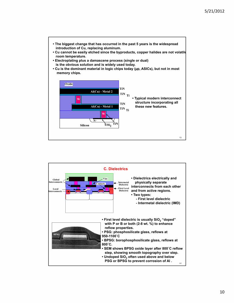
19
Al(Cu) - Metal 1TiTiN
TiN
TiN Ti
TiNAl(Cu) - Metal 2
Silicon TiSi2TiN
W
W
N+
Oxide
• Typical modern interconnect structure incorporating all these new features.
• The biggest change that has occurred in the past 5 years is the widespreadintroduction of Cu, replacing aluminum.
• Cu cannot be easily etched since the byproducts, copper halides are not volatileroom temperature.
• Electroplating plus a damascene process (single or dual) is the obvious solution and is widely used today.
• Cu is the dominant material in logic chips today (µp, ASICs), but not in most memory chips.
20
C. Dielectrics
LocalInterconnects
GlobalInterconnects
Vias
ContactsIntermetalDielectric
First LevelDielectric
• Dielectrics electrically andphysically separate
interconnects from each other and from active regions. • Two types:
- First level dielectric- Intermetal dielectric (IMD)
BPSG
• First level dielectric is usually SiO2 “doped” with P or B or both (2-8 wt. %) to enhance reflow properties.
• PSG: phosphosilicate glass, reflows at 950-1100˚C• BPSG: borophosphosilicate glass, reflows at 800˚C.• SEM shows BPSG oxide layer after 800˚C reflow
step, showing smooth topography over step. • Undoped SiO2 often used above and below
PSG or BPSG to prevent corrosion of Al .

5/21/2012
11
Fabrication Engineering at the Micro‐ and Nanoscale Campbell Copyright © 2009 by Oxford University Press, Inc.
Figure 15.1 Simple junction isolation in a bipolar transistor technologywith a common collector.
Fabrication Engineering at the Micro‐ and Nanoscale Campbell Copyright © 2009 by Oxford University Press, Inc.
Figure 15.3 Cross section of simple bipolar technology with a metal line crossing the junction isolation region, forming a parasitic MOSFET.
Figure 15.5Guard ring isolation for the bipolar technology from Figure 15.3.

5/21/2012
12
Fabrication Engineering at the Micro‐ and Nanoscale Campbell Copyright © 2009 by Oxford University Press, Inc.
Figure 15.6 Cross‐sectional views of a standard local oxidation of silicon(LOCOS) process.
Fabrication Engineering at the Micro‐ and Nanoscale Campbell Copyright © 2009 by Oxford University Press, Inc.
Figure 15.8 Cross‐sectional schematic of an MOS transistor cut along its width, illustrating the origin of narrow channel effects.

5/21/2012
13
Fabrication Engineering at the Micro‐ and Nanoscale Campbell Copyright © 2009 by Oxford University Press, Inc.
Figure 15.9 Simple shallow trench isolation process.
Figure 15.10
Deep trench isolation process schematic.
Fabrication Engineering at the Micro‐ and Nanoscale Campbell Copyright © 2009 by Oxford University Press, Inc.
Figure 15.10 Deep trench isolation process schematic.

5/21/2012
14
Fabrication Engineering at the Micro‐ and Nanoscale Campbell Copyright © 2009 by Oxford University Press, Inc.
Figure 15.12 Schematic of a shallow trench isolation module (after Chaterjee et al., used with permission, APS, 1997).
28
• Intermetal dielectrics also made primarily of SiO2
today, but cannot do reflow or densification anneals on pure SiO2 because of T limitations.
• Two common problems occur, cusping and voids, which can be minimized using appropriate deposition techniques.
-0.5
0.0
0.5
1.0
1.5
2.0
-1.00 1.000.0microns
-2.00 2.00
2.5
m i c r o n s
-0.5
0.0
0.5
1.0
1.5
2.0
-1.00 1.000.0microns
-2.00 2.00
2.5
m i c r o n s
• SPEEDIE simulations of silicondioxide depositions over a step for silane deposition (Sc = 0.4) and TEOS deposition (Sc = 0.1) showing less cusping in the lattercase.
b) Local planarization
c) Global planarization
Oxide
a) No planarization
• However planarization is also usually required today.

5/21/2012
15
29
Etchback tohereOxide
Photoresist
Silicon
Al Metal 1
SOG
CVDOxide
ViaAl - Metal 2
Silicon
AlMetal 1
Al - Metal 2
Via SOG
CVD Oxide
CVD Oxide
SOGSOG
CVD Oxide
CVD Oxide
Al Metal 1
Via
• One simple process involves planarizing with photoresist and then etching back with no selectivity.
• Spin-on-glass (SOG) is another option:• Fills like liquid photoresist, but becomes
SiO2 after bake and cure. • Done with or without etchback (with
etchback to prevent poisoned via - no SOG contact with metal).
• Can also use low-K SOD’s. (spin-on-dielectrics)
• SOG oxides not as good quality as thermal or CVD oxides
• Use sandwich layers.
• A final deposition option is HDPCVD which provides angle dependent sputtering during deposition which helps to planarize.
with etchback
without etchback
30
Wafer carrierWafer
Polishing pad
Polishing table
Slurry(facing down)
Close-up of wafer/pad interface:
Polishing pad(semi-rigid)
Silicon
Oxideslurry
Deposit thick oxide
Plasma etchback
Locally planarized topography remains
CMP
Globally planarized topography remains
• The most common solution today is CMP which works very well.
• It is capable of forming very flat surfacesas shown in the example below.

5/21/2012
16
31
Metal 1
Metal 2
W
Field OxideN+
W
Silicon
CVD SiO2BPSG
PECVD SiO2
PECVD SiO2
PECVD SiO2
CVD SiO2
With PECVD oxide/PECVD nitride passivation bilayeron top of final metal level
PECVD SiO2
SOG or SOD
SOG or SOD
• Backend structure showing one possible dielectric multi-structurescheme. Other variations includeHDP oxide or the use of CMP.
• Two backend structures. Left: three metal levels and encapsulated BPSG for the first level dielectric; SOG (encapsulated top and bottom with PECVD oxide) and CMP in the intermetal dielectrics. The multilayer metal layers and W plugs are alsoclearly seen. Right: five metal levels, HDP oxide (with PECVD oxide on top) and
CMP in the intermetal dielectrics.
Fabrication Engineering at the Micro‐ and Nanoscale Campbell Copyright © 2009 by Oxford University Press, Inc.
Figure 15.13 Dielectric isolation (DI) process for forming silicon on insulator.

5/21/2012
17
33
THE FUTURE OF BACKEND TECHNOLOGY
L 0.89RC 0.89 KIKoxoL2 1
Hxox
1
WLS
• Remember: (1)
• Reduce metal resistivity - use Cu instead of Al.• Aspect ratio - advanced deposition, etching and planarization methods.• Reduce dielectric constant - use low-K materials.
Year of Production 1998 2000 2002 2004 2007 2010 2013 2016 2018
Technology N ode (half pi tch) 250 nm 180 nm 130 nm 90 nm 65 nm 45 nm 32 nm 22 nm 18 nm
MPU Printed Gate Length 100 nm 70 nm 53 nm 35 nm 25 nm 18 nm 13 nm 10 nm
Min Meta l 1 Pitch (nm) 214 152 108 76 54 42
Wiring Levels - Logic 10 11 12 12 14 14
Metal 1 Aspect Ratio (Cu) 1.7 1.7 1.8 1.9 2.0 2.0
Contact As pec t Ratio (DRAM) 15 16 >20 >20 >20 >20
STI Trenc h As pec t Ratio 4.8 5.9 7.9 10.3 14 16.4
Metal Res istivi ty (µohm-cm) 3.3, 2.2 2.2 2.2 2.2 2.2 2.2 2.2 2.2 2.2
Interlevel Dielectric Constant 3.9 3.7 3.7 <2.7 <2.4 <2.1 <1.9 <1.7 <1.7
34
Material class Material Dielectricconstant
Depositiontechnique
Inorganic SiO2 (including PSGand BPSG)
3.9-5.0 CVD/Thermalox./Bias-
sputtering/HDP
Spin-on-glass (SiO2)(including PSG, BPSG)
3.9-5.0 SOD
Modified SiO2
(e.g. fluorinated SiO2
or hydrogensilsesquioxane - HSQ)
2.8-3.8 CVD/SOD
BN (Si) >2.9 CVDSi3N4 (only used in
multilayer structure)5.8-6.1 CVD
Organic Polyimides 2.9-3.9 SOD/CVDFluorinated polyimides 2.3-2.8 SOD/CVD
Fluoro-polymers 1.8-2.2 SOD/CVDF-doped amorphous C 2.0-2.5 CVD
Inorganic/Org-anic Hybrids
Si-O-C hybridpolymers based on
organo-silsesquioxanes(e.g. MSQ)
2.0-3.8 SOD
Aerogels(Microporous)
Porous SiO2 (with tinyfree space regions)
1.2-1.8 SOD
Air bridge 1.0-1.2
• All of these approaches are beginning to appear in advanced process flows today.

5/21/2012
18
35
Summary of Key Ideas• Backend processing (interconnects and dielectrics) have taken on increased
importance in recent years.
• Interconnect delays now contribute a significant component to overall circuit performance in many applications.
• Early backend structures utilized simple Al to silicon contacts.
• Reliability issues, the need for many levels of interconnect and planarization issues have led to much more complex structures today involving multilayer metals and dielectrics.
• CMP is the most common planarization technique today.
• Copper and low-K dielectrics are now found in some advanced chips and their use will likely be common in the future.
• Beyond these materials changes, interconnect options in the future include architectural (design) approaches to minimizing wire lengths, opticalinterconnects, electrical repeaters and RF broadcasting. All of these areas will see significant research in the next few years.
Fabrication Engineering at the Micro‐ and Nanoscale Campbell Copyright © 2009 by Oxford University Press, Inc.
Chapter 20
Integrated Circuit Manufacturing
5/21/2012
19
• Contamination, Defects & Distributions
• Yield• uniform defects• non-uniform defects• multiple defect types
• Reliability & Failure• distributions and plotting• target failure rates • accelerated testing
• Objective: Can use reliability statistics with various models
Faulty circuits by:- Processing faults:- thickness variations, oxide, poly-Si- residues- Circuit tolerances may be exceeded by
device variation by minor processing variations. - Dirt etc:
- during lithography or metallization etc. - may have missing parts of circuit.- importance of clean room, water, etc.

5/21/2012
20
39
SEMICONDUCTOR MANUFACTURING: YIELD,CLEAN ROOMS, WAFER CLEANING, GETTERING, SPC, DOE, CIM
• Modern IC factories employ a three tiered approach to controlling unwanted impurities: 1. clean factories 2. wafer cleaning 3. gettering
Silicon Wafer
SiO2 or other thin films
PhotoresistAu
Cu
Fe
Particles
Interconnect Metal
Na
N, P
• Contaminants may consist of particles, organic films (photoresist), heavy metals or alkali ions.
Year of Production 1998 2000 2002 2004 2007 2010 2013 2016 2018
Technology N ode (half pi tch) 250 nm 180 nm 130 nm 90 nm 65 nm 45 nm 32 nm 22 nm 18 nm
MPU Printed Gate Length 100 nm 70 nm 53 nm 35 nm 25 nm 18 nm 13 nm 10 nm
DRAM Bits/Chip (Sampling) 256M 512M 1G 4G 16G 32G 64G 128G 128G
MPU Trans istors/Chip (x106) 550 1100 2200 4400 8800 14,000
Critical Defec t Si ze 125 nm 90 nm 90 nm 90 nm 90 nm 90 nm 65 nm 45 nm 45 nm
Starting Wafe r Particle s (cm-2 ) <0.35 <0.18 <0.09 <0.09 <0.05 <0.05
Starting Wafe r Total Bulk Fe (cm-3 ) 3x10¹⁰ 1x10¹⁰ 1x10¹⁰ 1x10¹⁰ 1x10¹⁰ 1x10¹⁰ 1x10¹⁰ 1x10¹⁰ 1x10¹⁰
Metal Atom s on Wafer Surface
After Clean ing (cm-2 )
5x10⁹ 1x10¹⁰ 1x10¹⁰ 1x10¹⁰ 1x10¹⁰ 1x10¹⁰ 1x10¹⁰ 1x10¹⁰ 1x10¹⁰
Particles on Wafe r Surface After
Clean ing (#/ wafer)
75 80 86 195 106 168
2003 ITRS Front End processes
40
Example #1: MOS VTH is given by VTH VFB 2 f
2SqN A (2 f )
CO
qQ M
CO
(1)
If tox = 10 nm, then a 0.1 volt Vth shift can be caused by QM = 6.5 x 1011 cm-2 (< 0.1% monolayer or 10 ppm in the oxide).
Example #2: MOS DRAM
- - - -- --- -- -- STORED
CHARGEON MOS
CAPACITOR
ACCESSMOS
TRANSISTOR
BIT LINE
WORDLINE
• Refresh time of several msec requires a generation lifetime of
sec 1001
tthNv
(2)
• This requires trap densityNt ≥ 1012 cm-3 or ≤ 0.02 ppb.
•Traps typically Au, Fe, Cu impurities
Contamination

5/21/2012
21
41
Level 1 Contamination Reduction: Clean Factories
.
1
1 0
100
1000
1 04
1 05
1 06
1 07
0 . 1 1 1 0 100
T o t a l P a r t i c l e s P e r C u b i c F o o t
Particle Size (µm)
100,000
10,000
1000
100
1 01
• Air quality is measured by the “class” of the facility.
(Photo courtesy of Stanford Nanofabrication Facility.)
Factory environment is cleaned by:• Hepa filters and recirculation for the air,• “Bunny suits” for workers.• Filtration of chemicals and gases.• Manufacturing protocols.
Number of larger particles
42
Level 2 Contamination Reduction: Wafer Cleaning
• RCA clean is “standard process” used to remove organics, heavy metals and alkali ions.
• Ultrasonic agitation is used to dislodge particles.
120 - 150ÞC 10 min
Strips organics especially photoresist
DI H2O Rinse Room T
80 - 90ÞC 10 min
Strips organics, metals and particles
DI H2O Rinse Room T
80 - 90ÞC 10 min
Strips alkali ions and metals
Room T 1 min
Strips chemical oxide
DI H2O Rinse Room T
H2SO4/H2O2 1:1 to 4:1
HF/H2O 1:10 to 1:50
NH4OH/H2O2/H2O 1:1:5 to 0.05:1:5
SC-1
HCl/H2O2/H2O 1:1:6 SC-2

5/21/2012
22
43
Modeling Wafer Cleaning• Cleaning involves removing particles, organics (photoresist) and metals from
wafer surfaces.• Particles are largely removed by ultrasonic agitation during cleaning.• Organics like photoresists are removed in an O2 plasma or in H2SO4/H2O2 solutions• The “RCA clean” is used to remove metals and any remaining organics.• Metal cleaning can be understood in terms of the following chemistry.
Si 2H 2O SiO 2 4H 4e
M Mz ze
(5)
(6)
• If we have a water solution with a Si wafer and metal atoms and ions, the stronger reaction will dominate.
• Generally (6) is driven to the left and (5) to the right so that SiO2 is formed and M plates out on the wafer.
• Good cleaning solutions drive (6) to the right since M+ is soluble and will be desorbed from the wafer surface.
44
Oxidant/Reductant
StandardOxidation
Potential (volts)
Oxidation-Reduction Reaction
Mn2+/Mn 1.05 Mn Mn2 2e
SiO2/Si 0.84 Si 2H2O SiO2 4H 4e
Cr3 Cr Cr3 3e
Ni2 Ni Ni2 2e
Fe3 Fe Fe3 3e
H2SO4 H2O H2SO3 H2SO4 2H 2e
Cu2 Cu Cu2 2e
O2 2H2O O2 4H 2e
Au3 Au Au3 3e
H2O2 2H2O H2O2 2H 2e
O3 O2 H2O O3 2H 2e
• The strongest oxidants are at the bottom (H2O2 and O3). These reactions go to the left grabbing e- and forcing (6) to the right.
• Fundamentally the RCA clean works by using H2O2 as a strong oxidant.

5/21/2012
23
45
Level 3 Contamination Reduction: Gettering
• Gettering is used to remove metal ions and alkali ions from device active regions.
H 1.008
1
3 4
11 12
19 20
Li 6.941
Be 9.012
Na 22.99
Mg 24.31
K 39.10
Ca 40.08
Rb 85.47
Cs 132.9
Fr 223
Sr 87.62
Ba 137.3
Ra 226
37 38
55 56
87 88
Sc 44.96
Ti 47.88
V 50.94
Cr 51.99
Mn 54.94
Fe 55.85
Co 58.93
Ni 58.69
Cu 63.55
Zn 65.39
21 22 23 24 25 26 27 28 29 30
Y 88.91
Zr 91.22
Nb 92.91
Mo 95.94
Tc 98
Ru 101.1
Rh 102.9
Pd 106.4
Ag 107.9
Cd 112.4
39 40 41 42 43 44 45 46 47 48
La 138.9
Hf 178.5
Ta 180.8
W 183.9
Re 186.2
Os 190.2
Ir 192.2
Pt 195.1
Au 197.0
Hg 200.6
57 72 73 74 75 76 77 78 79 80
Ac 227.0
Unq 261
Unp 262
Unh 263
Uns 262
89 104 105 106 107
B 10.81
Al 26.98
Ga 69.72
In 114.8
Tl 204.4
C 12.01
Si 28.09
Ge 72.59
Sn 118.7
Pb 207.2
N 14.01
P 30.97
As 74.92
Sb 121.8
Bi 209.0
O 16.00
S 32.06
Se 78.96
Te 127.6
Po 209
F 19.00
Cl 35.45
Br 79.90
I 126.9
At 210
He 4.003
Ne 20.18
Ar 39.95
Kr 83.80
Xe 131.3
Rn 222
5 6 7 8 9 10
2
13 14 15 16 17 18
31 32 33 34 35 36
49 50 51 52 53 54
81 82 83 84 85 86
Period
1
2
3
4
5
6
7
I A
II A
IIIB
IVB
VA
I BII B
III A IV A
VB
VIB
VIIB
VIII
VI A VII A
Noble Gases
Sh
allo
w D
onor
s
Sh
allo
w A
ccep
tors
Ele
men
tal
Sem
icon
du
ctor
s
Deep Level Impurites in Silicon
Alkali Ions
• For the alkali ions, gettering generally uses dielectric layers on the topside (PSG or barrier Si3N4 layers).
• For metal ions, gettering generally uses traps on the wafer backside or in the wafer bulk.
• Backside = extrinsic gettering. Bulk = intrinsic gettering.
46
.
10 -20
10 -18
10 -16
10 -14
10 -12
10 -10
10 -8
10 -6
0.65 0.7 0.75 0.8 0.85 0.9 0.95 1
1000/T (Kelvin)
SiAs
B, P
AuS
Cr
Pt
Fe
AuI
Cu
1200 1100 1000 900 800T (ÞC)
InterstitialDiffusers
Dopants
Ti
Diffusivity (cm
2
sec-
1)
I Diffusivity
10 -4
• Heavy metal gettering relies on:• Metals diffusing very rapidly in silicon.• Metals segregating to “trap” sites.
Devices in nearsurface region
Denuded Zoneor Epi Layer
IntrinsicGetteringRegion
BacksideGetteringRegion
10 - 20 µm
500+ µm
PSGLayer
1
2
3
*3
Trapping
*Trapping
Aus Aui
Diffusion
• Gettering consists of1. Making metal atoms mobile.2. Migration of these atoms to trapping sites.3. Trapping of atoms.
• Step 1 generally happens by kicking out the substitutional atom into an interstitial site. One possible reaction is:
• Step 2 usually happens easily once the metal is interstitial since most metals diffuse rapidly in this form.• Step 3 happens because heavy metals segregate preferentially to damaged regions or to N+ regions or pair with effective getters like P (AuP pairs).
• In intrinsic gettering, the metal atoms segregate to dislocations around SiO2 precipitates.

5/21/2012
24
47
500
700
900
1100
T e m p e r a t u r e
Þ
C
Time
Outdiffusion
Nucleation
Precipitation
• “Trap” sites can be created by SiO2 precipitates (intrinsic gettering), or by backside damage (extrinsic gettering).
• In intrinsic gettering, CZ silicon is used and SiO2
precipitates are formed in the wafer bulk throughtemperature cycling at the start of the process.
StackingFault
V I
OI Diffusion
[OI]
SiO2
OI
OI
OIOI
OI SiO2
(See Chapter 3 class notes)
SiO2 precipitates (white dots) in bulkof wafer.
Intrinsic gettering cycle
Fabrication Engineering at the Micro‐ and Nanoscale Campbell Copyright © 2009 by Oxford University Press, Inc.
Figure 20.1 A plot of yield versus lot number for a particular technology. Also shown is the running average for the last seven lots.
Typical “learning curve”
Defects&
Yield
5/21/2012
25
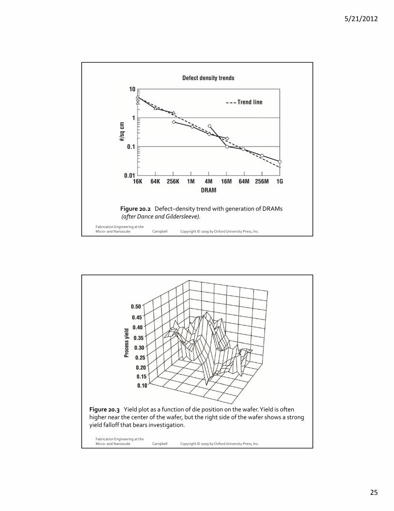
Fabrication Engineering at the Micro‐ and Nanoscale Campbell Copyright © 2009 by Oxford University Press, Inc.
Figure 20.2 Defect–density trend with generation of DRAMs(after Dance and Gildersleeve).
Fabrication Engineering at the Micro‐ and Nanoscale Campbell Copyright © 2009 by Oxford University Press, Inc.
Figure 20.3 Yield plot as a function of die position on the wafer. Yield is often higher near the center of the wafer, but the right side of the wafer shows a strong yield falloff that bears investigation.

5/21/2012
26
Fabrication Engineering at the Micro‐ and Nanoscale Campbell Copyright © 2009 by Oxford University Press, Inc.
Figure 20.4 Meander lines and interdigitated comb structures used to determine a layer defect density.
Process control modules: Highlight (contamination) defects
Fabrication Engineering at the Micro‐ and Nanoscale Campbell Copyright © 2009 by Oxford University Press, Inc.
Figure 20.6 Two typical fault kernel curves
5/21/2012
27
53
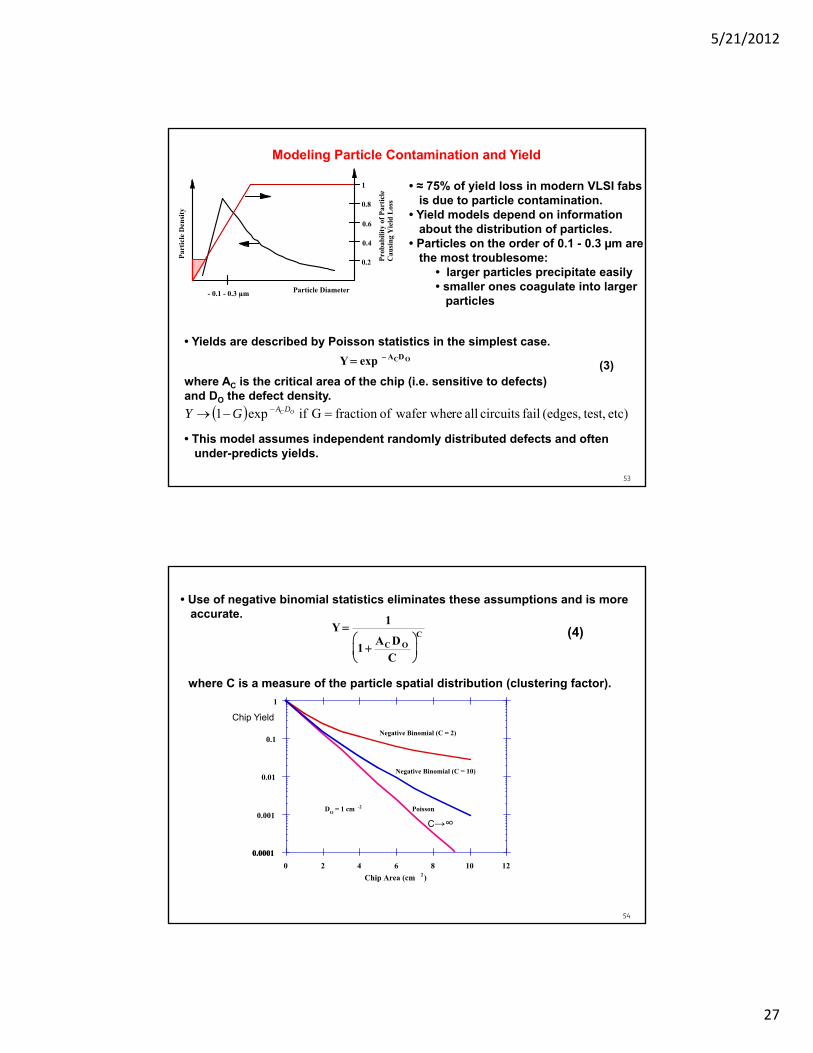
Modeling Particle Contamination and Yield
• ≈ 75% of yield loss in modern VLSI fabs is due to particle contamination.
• Yield models depend on information about the distribution of particles.
• Particles on the order of 0.1 - 0.3 µm are the most troublesome:
• larger particles precipitate easily• smaller ones coagulate into larger
particlesParticle Diameter
Par
ticl
e D
ensi
ty
- 0.1 - 0.3 µm
Pro
bab
ilit
y of
Par
ticl
e
Cau
sin
g Y
ield
Los
s
0.2
0.4
0.6
0.8
1
• Yields are described by Poisson statistics in the simplest case.
Y exp ACD O(3)
where AC is the critical area of the chip (i.e. sensitive to defects) and DO the defect density.
• This model assumes independent randomly distributed defects and often under-predicts yields.
etc) test,(edges, fail circuits all re wafer wheoffraction G if exp1 OC DAGY
54
• Use of negative binomial statistics eliminates these assumptions and is more accurate.
Y 1
1 AC D O
C
C (4)
where C is a measure of the particle spatial distribution (clustering factor).
0.0001
0.001
0.01
0.1
1
0 2 4 6 8 10 12
0.0001
Chip Area (cm 2)
Poisson
Negative Binomial (C = 2)
Negative Binomial (C = 10)
DO = 1 cm -2
Chip Yield
C→∞

5/21/2012
28
55
.
0 .0 1
0. 1
1
0 5 1 0 15 20
Ch i p Yield
Chip A rea (cm2)
19 97 2 00 6 2012
Do = 0.01 cm-2
D o = 1 cm-2
Do = 0.1 cm-2
• Vertical lines are estimated chip sizes (from the ITRS).
• Note that defect densities will need to be extremely small in the future to achieve the high yields required for economic IC manufacturing.
• (See particle defect densities)
i
ii
Clevels
i i
C
C
DAYyieldOverall
1
01
Fabrication Engineering at the Micro‐ and Nanoscale Campbell Copyright © 2009 by Oxford University Press, Inc.
Figure 20.5 Theoretical and measured particle density as a function of particle diameter (after deGyvez).
Defect sizes
max
max0
10
010
for 0
for
0for
size
p
p
size
q
q
size
D
CD
CD
5/21/2012
29
Fabrication Engineering at the Micro‐ and Nanoscale Campbell Copyright © 2009 by Oxford University Press, Inc.
Figure 20.7 An overlay of the fault kernel (broken lines) and the defect distribution (solid lines). Small shifts in the fault kernel curve can lead to dramatic changes in the yield.
ADi
levels
ii
size
AD
iieGYY
K(x)
dxxKxD
GY
)1(
kernely probabilitfault
,)()(
fatal isdefect sizemean
y that probabilit averagedfor
exp1
1
0
Assume defects uniformly distributed.
xx
x
x
x
x
x
x
x
x 24 chips,10 defects --> 8 chip fails, 16 good

5/21/2012
30
Problem is: Place n balls in N cells. Calculate probability that a given cell contains k balls.
For n defects spread over N chips on wafer, probability that given chip contains k defects
= Pk = n! / (k! (n-k)!) N-n (N-1) n-k
(Binomial distribution)
e-m mk / k! (Poisson distribution)for n & N large, n/N = m finite
Yield = Probability that chip contains no defects = Y1 = Po = e-m
ie. PoxN good chips on wafer
Prob. that chip contains one defect = P1 = me-m
If chip area = A, total number of chips = N, then total area = NA, & Defect density D0 = n/NA Avg no of defects/chip= n/N = m = D0NA/N =DoA
Y1 = P0 = e-D0A
In practice this value is much too low. Fallacy lies in random distribution of defects. In practice, processing problems tend to cluster in given area.
5/21/2012
31
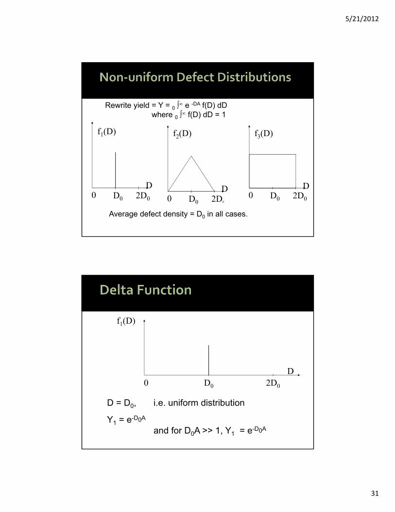
Rewrite yield = Y = 0 e -DA f(D) dDwhere 0 f(D) dD = 1
Average defect density = D0 in all cases.
0 D0 2D0
D
f1(D)
0 D0 2D0
D
f2(D)
0 D0 2D0
D
f3(D)
0 D0 2D0
D
f1(D)
D = D0, i.e. uniform distribution
Y1 = e-D0A
and for D0A >> 1, Y1 = e-D0A
5/21/2012
32
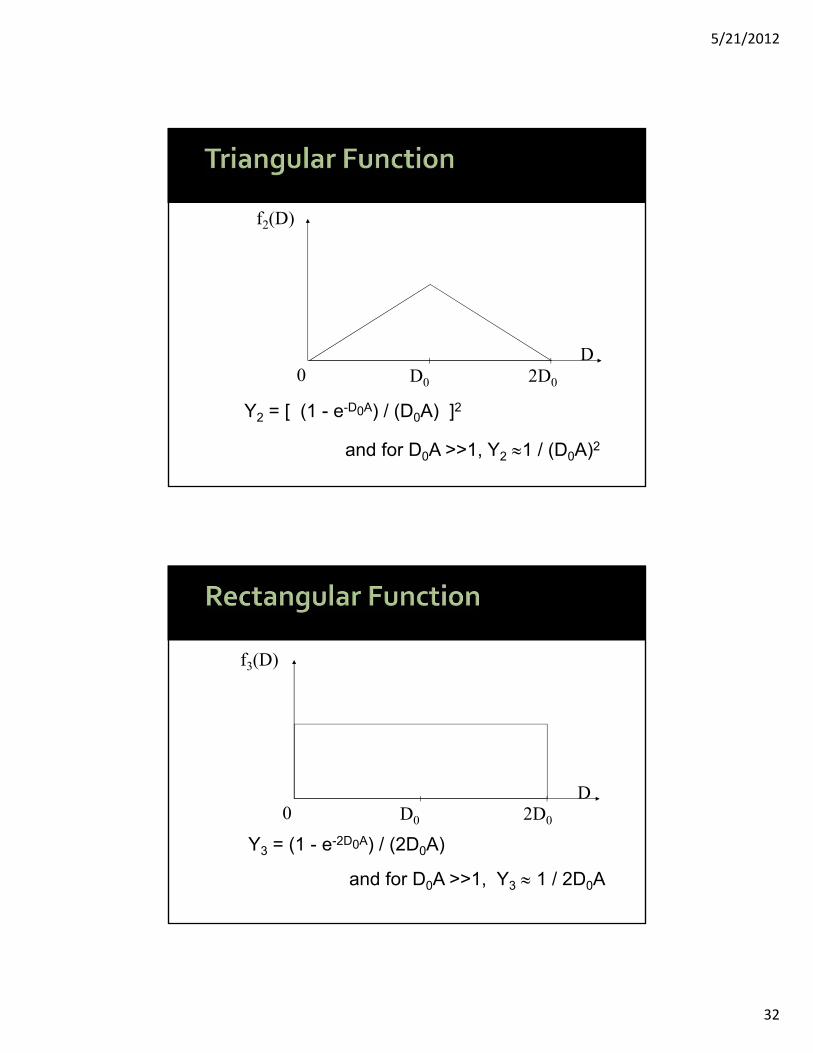
Y2 = [ (1 - e-D0A) / (D0A) ]2
and for D0A >>1, Y2 1 / (D0A)2
0 D0 2D0
D
f2(D)
0 D0 2D0
D
f3(D)
Y3 = (1 - e-2D0A) / (2D0A)
and for D0A >>1, Y3 1 / 2D0A

5/21/2012
33
Y1 = exp - D0A
Y2 = (D0A)-2
Y3 = (2D0A)-1
& Y2, Y3 >> Y1
ie. not as pessimistic as Y1
f4(D) = (() ) -1 D -1 e -D/
Average density D0 = variance in D = 2
coeff. of variation = (var (D) )1/2 /D0
= ()1/2 / = 1 / 1/2
Probability of chip having k defects,Pk = 0 e-m (mk/ k! ) f(D) dD
= [(k+ ) / (k! ())].[(A)k / (A+1)k+ ]

5/21/2012
34
Probability of no defects on given chip Y4 = P0 = 1 / (A + 1) = 1 / (1+SAD0)1/s
where S = var(D) / D02 = 1/
0 D0 2D0
D
f4(D)
S = .1
1
.8 .4
For s=1, =1: f4(D) = -1 e-D/B, Y4 = (1+ADo) -1
For s=0, =: f4(D) --> (D-D0)
= f1(D) Y4 --> Y1
D0A
321 4.01
.1
1
Y4 (S = 1)
Y3
Y2
Y1

5/21/2012
35
Yield with redundant circuit designed into chip:
Y1 = P0 + P1
P0 is defect probabilityP1 is probability of one defect is probability that one defect can be “repaired”
by redundancy.
In practice, each type of defect has its own distribution function
eg. Thin gate oxide, metal opens, etc.
i.e. each defect “n” ---> mean defect density D0 --> Dno
---> distribution shape factor S --> Sn
---> total chip area susceptible to defectA --> An
for each type of defect n, Yn = (1+SnAnDno) -1/Sn
overall yield Y=n=1N Yn=n=1N (1+SnAnDno)-1/Sn

5/21/2012
36
If SnAnDno << 1, ie. yn --> 1 for all individual defect types, ie. process has been well characterized,
defects minimized, controlled etc.,
ln Y = n=1N - Sn-1 ln (1+SnAnDno)
n=1N - Sn-1 (SnAnD0) = n=1N - AnDno
Y exp(- n=1N AnDno) = exp - ADm
where Dm = A-1n=1N AnDno
ie. yield is exponential, independent of shape parameters Sn
provided SnAnDno<<1. Dm function of circuit type due to An
Dm varies with circuit type
Many defect types have radial dependence, especially handling, misalignment, photoresistresidue, etc.
D( r) = D0 + DR e(r-R)/L , D0 defect density at center, DR increase at edge, r radial coordinate, R wafer radius, L characteristic length for edge defects
YR = (R2)-10R Y dA, (A=r2, dA=2r dr)
--> integrate Poisson yield factor over wafer= 1 / (R2) 0 R e -D(r ) A 2r dr= 2R -2 0 R e-D(r )A r dr

5/21/2012
37
73
Summary of Key Ideas
• A three-tiered approach is used to minimize contamination in wafer processing.
• Particle control, wafer cleaning and gettering are some of the "nuts and bolts" of chip manufacturing.
• The economic success (i.e. chip yields) of companies manufacturing chips todaydepends on careful attention to these issues.
• Level 1 control - clean factories through air filtration and highly purified chemicals and gases.
• Level 2 control - wafer cleaning using basic chemistry to remove unwanted elements from wafer surfaces.
• Level 3 control - gettering to collect metal atoms in regions of the wafer far away from active devices.
• The bottom line is chip yield. Since "bad" die are manufactured alongside "good" die, increasing yield leads to better profitability in manufacturing chips.
Fabrication Engineering at the Micro‐ and Nanoscale Campbell Copyright © 2009 by Oxford University Press, Inc.
Figure 20.9 A schematic of a semiconductor process. Both controlled and uncontrolled variables must be considered.
Statistical Process Control (SPC)
Continuously gather data on all processes.Compare to previous and performance.

5/21/2012
38
Fabrication Engineering at the Micro‐ and Nanoscale Campbell Copyright © 2009 by Oxford University Press, Inc.
Figure 20.10 Etch rate of a plasma system as a function of power and pressure.
Full Factorial experiments (ANOVA)
2 variables. In practice, many more, and data (number of tests) rapidly escalates.
Fabrication Engineering at the Micro‐ and Nanoscale Campbell Copyright © 2009 by Oxford University Press, Inc.
Figure 20.11 Particle counts as a function of silane flow and chamber pressure for the low pressure deposition of polysilicon (after DePinto).
Design of experiments (DOE) for more complex (limits data)
1. Identify all variables. 2. “Screening” experiments (to identify “weak” effects.) 3. 2nd, 3rd experiment sequences on significant parameters.
(Nominal P-40mτ)
(Nominal P)
(Nominal P-80mτ)
(45% flow) (35% flow)
Note variation with P …. “confounded”
Interpretation difficult with few experiments

5/21/2012
39
Fabrication Engineering at the Micro‐ and Nanoscale Campbell Copyright © 2009 by Oxford University Press, Inc.
Figure 20.12 A full CIM system implemented by one major semiconductor manufacturer(from Mizokami).
Computer Integrated Manufacturing (CIM)
Fabrication Engineering at the Micro‐ and Nanoscale Campbell Copyright © 2009 by Oxford University Press, Inc.
Figure 20.13 Charts showing the remaining lot moves as a function of time areoften used to point out bottlenecks in the line. These diagrams are sometimescalled chicken scratches.
↓ Process bottleneck

5/21/2012
40
Say 100,000 components in systemSay < 1 failure/month < 1 failure / 105 devices x 720 hours
= 14 x10-9 failures / device hr
Define 1 Failure unIT (FIT) = 1 failure/10 9 device hrs.
10 FIT --> < 1 service call/month (target)100 FIT --> < 1 service call/ 4-5 days (OK)1000 FIT --> ~ 2-3 service calls/ day
(unacceptable)
100,000 devicesFIT Fails/month % failures in
10yr life10 0.7 0.1%100 7.0 1%
1000 70 10%
10,000 devicesFIT Fails/month % systems
failing/month10 0.07 1%100 0.7 10%
1000 7.0 65%

5/21/2012
41
100 devices on testFIT Time to
1st failure10 114 yrs100 11 yrs1000 1 yr
Run 500 devices for 6 monthsConfidencelevel (%)
Failure rate(FIT)
99 210095 140090 110060 430Best estimate 325
200 devicesFIT MTTF
(years)% systems
failing/month10 51 0.16%
100 5 1.6%1000 0.5 16%
For 100 FITmust wait 114 years for 1 device from 100 to fail.
Need 105 - 1011 hrs (depends on ) for median life.
Obviously need to speed up failure rates & relate back.

5/21/2012
42
Failure mechanisms chemical etc: Rate R=R0exp-E/ktSpeed up by increasing T Accel = R2/R1 = t1/t2
=exp(E/k)(T1-1-T2
-1)
Failure
Parameters
tt2 t1
T2 T1
T2 > T1t2 < t1
Find Ea for time to failure & TtF = const * exp Ea/kTln tF = const + Ea/kT
Then can extrapolate times back to normal T
Incr T(C)
Acceleration factor Time equiv to 40 yrs(hrs)
Ea=1eV Ea=0.5eV Ea=1eV Ea=0.5eV85 11.5 3.4 30,000 103,000125 300 17 1200 20,200150 1700 41 200 8,526200 31,000 176 11 2,000250 320,000 570 1.1 616300 2,200,00 1500 0.2 233

5/21/2012
43
Voltage/CurrentRate R(T, V) = R0(T).V(T) ~ 1 --> 4.5
Cannot get much acceleration with practical device voltages.
Dielectric breakdown ---> more burn in
Humidity
Burn inEFF(t) = (t+)
eff
without burn in
With burn in
• Contamination
•Defect distributions
• Yield statistics for various defect models
•Modeling, SPC, DOE, & CIM
• Failure statistics & Accelerated testing
•(Reliability Theory)
5/21/2012
44
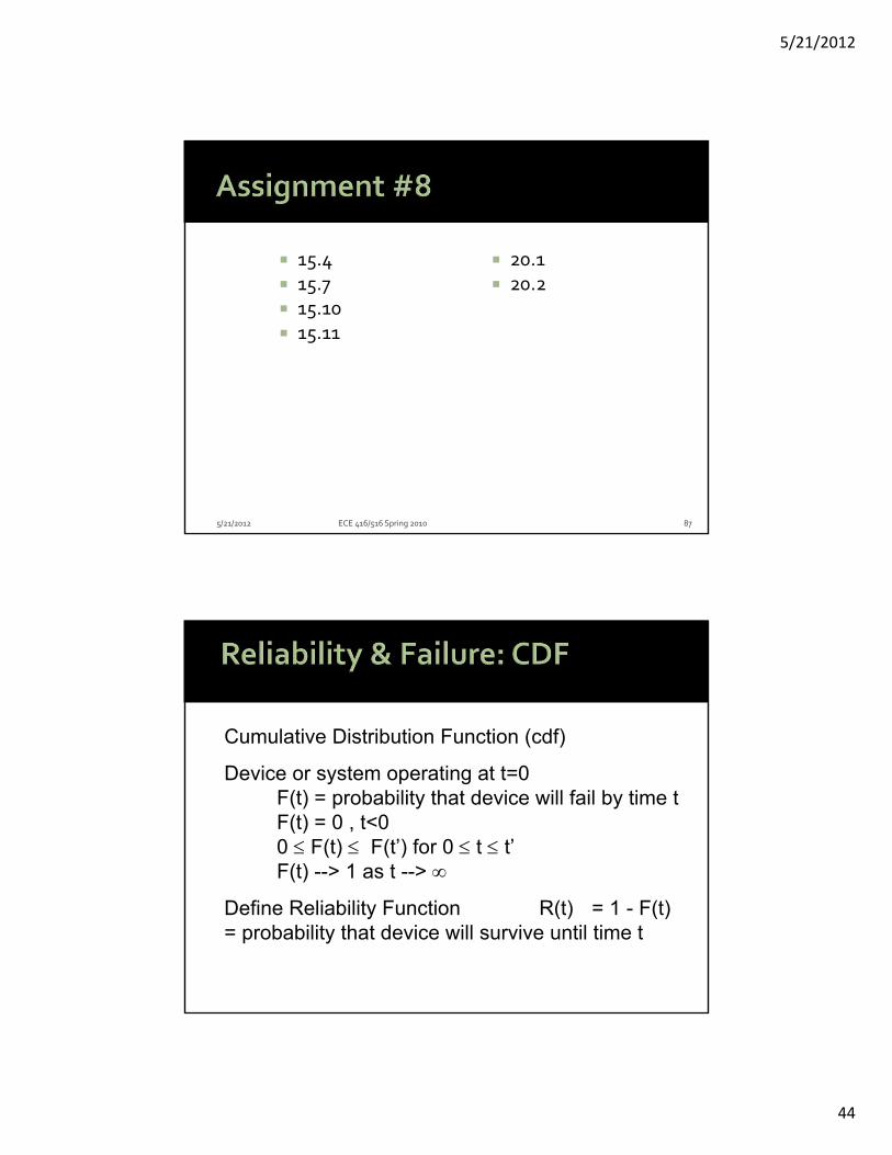
15.4 15.7 15.10 15.11
20.1 20.2
5/21/2012 ECE 416/516 Spring 2010 87
Cumulative Distribution Function (cdf)
Device or system operating at t=0F(t) = probability that device will fail by time tF(t) = 0 , t<00 F(t) F(t’) for 0 t t’F(t) --> 1 as t -->
Define Reliability Function R(t) = 1 - F(t) = probability that device will survive until time t

5/21/2012
45
Probability Density Function (pdf) f (t) = dF(t) /dt
ie. F(t) = 0t f(x) dx R(t) = 1 - F(t)
= 0 f(x) dx - 0 t f(x) dx = t f(x) dx
f(t) = d/dt (1 - R(t)) = - d/dt R(t)
Failure Rate (Hazard Rate) i.e. instantaneous failure rate (not average)
F(t+t) - F(t) = R(t) - R(t+t) =fraction of devices good at t which fail by t+t
Average failure rate during t = (1 / t) [ (R(t) - R(t+t)) / R(t) ] = (t) , because divide by number left at t
as t --> 0, (t) --> R(t)-1 dR(t)/dt
= - d/dt ln R(t) = f(t)/R(t) = f(t)/(1-F(t))ie. R(t) = exp [-0t (x) dx ]
instantaneous failure rate

5/21/2012
46
Mean time to failure (MTTF) = mean time between failures MTB
if repair assumed
MTTF = 0 t f(t) dt
ie. average age at failure
wear out
steady stateearly failure/infant mortality
(t)
Not normally observed in ICs.
Improve by
failure random, many possible unrelated causesburn in

5/21/2012
47
(t) = 0 constant
R(t) = e -o t & F(t) = 1 - e -o t
f(t) = d/dt F(t) = 0 e -o t
& MTTF = 0 t 0e- o t dt
= 0 [ t e -o t / - 0 - 0 e- o t / -0 dt]
= [ -te -o t + e -o t / - 0 ]0 = 1 / 0
Weibull Distribution function Failure rate tpower
(t) = (/) t -1
< 1 failure rate decr with t (early failures) > 1 failure rate increases with t (wear out) = 1 failure rate constant
R(t) = exp-0t(/) t -1dt= exp -/. t/ = exp-t/
F(t) = 1 - e-t /
f(t) = (-e-t / )((- t -1)/ ) = (/) t -1 exp - t /

5/21/2012
48
Notes (I) If some time of device life expired due to device test, etc,
Write t = t’ +
(ii) Weibull plotting paper: 1 - F(t) = e-t /
ln (1 - F(t)) = -t /
ln{ln[1 / (1-F(t))] } = ln t - ln
Cum % failed F(t)
ln ln (100- xxx)/(100 - % failed)
.1
90
3010
1
95
Plot average failure rate (AFR) vs log tAFR = Fraction of failed devices/t=F(t)/t
If plot is straight line, negative slope:ln AFR = -s ln t + ln k
implies AFR = F(t)/t = k t -S
F(t) = k t1-S, f(t) = k(1-s)t-S
(t) = f(t)/(1-F(t)) = (k(1-s)t-S) / (1-kt1-S) If only few devices have failed F(t) << 1
(t) k (1-s) t -S = (1-s) AFRCompare Weibull with = 1-s, = 1/k, but cannot extrapolate shorter Duame plot for F(t) << 1 to long term where inequality fails.
5/21/2012
49
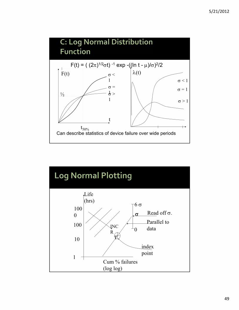
F(t) = ( (2)1/2t) -1 exp -((ln t - )/)2/2
Can describe statistics of device failure over wide periods
F(t)
t50%
t
½
< 1
= 1 > 1 > 1
= 1
< 1
(t)
INCR
T
Life (hrs)
1000
100
1
10
0
Cum % failures (log log)
6
Read off .
Parallel to data
index point

5/21/2012
50
Bimodal - log normalT(t) = S(t) * fraction of sports
+ M(t) * fraction of main population
.5 2 10 30 50 70 90 98
combined
10% "sport" distrib
Main distrib 90%
10-1
100
101
102
103
104