ece 3610 microprocessing systems lab #1 verilog...
TRANSCRIPT

ECE 3610 Microprocessing Systems
Lab #1
Verilog Design of the TOC Using Quartus II
This lab manual presents an introduction to the Quartus® II Computer Aided Design (CAD)
system. This manual gives step-by-step instructions for using the Quartus II software to implement
a part of the Tiny Operation Set Calculator (TOC) in Altera’s DE board. Students have the option
to extend the lab by completing the Verilog descriptions for the other components of the TOC, and
implementing and testing the TOC on the DE2 board.
The Quartus II system includes full support for all of the popular methods of entering a
description of a desired circuit into a CAD system. Designs can be described and entered using
three methods: (i) the Verilog hardware description language, (ii) the VHDL hardware description
language, and (iii) schematic diagram entry. This lab makes use of the Verilog design entry
method, in which the user specifies the desired circuit in the Verilog hardware description
language.
Each of the workstations has Quartus II software installed on it, and the workstation may be
connected to the Altera DE2 Development and Education board via a USB cable. A reader who
does not have access to the DE2 board will still find the lab manual useful to learn how to use the
Quartus II software and how to program the FPGA on the DE2 board.
The screen captures in this lab manual were obtained using the Quartus II version 12.1; if other
versions of the software are used, some of the images may be slightly different.
This lab manual introduces the basic features of the Quartus II software. It shows how the
software can be used to design and implement a circuit specified by using the Verilog hardware
description language. It makes use of the graphical user interface to invoke the Quartus II
commands. The reader will learn about:
Creating a project
Design entry using Verilog code
Synthesizing a circuit specified in Verilog code
Assigning the circuit inputs and outputs to specific pins on the FPGA
Programming the FPGA chip on Altera’s DE2 board
Testing the circuit
1. Getting Started
A logic circuit being designed with Quartus II software is called a project. The software works
on one project at a time and keeps all information for that project in a single directory (folder) in
the file system. To begin a new logic circuit design, the first step is to create a directory to hold its
files. To hold the 5 projects for this lab, we will store them in separate folders under the top-level
directory called c:\ECE3610\Labs\Lab1\. Using the OS, create this top-level directory now.
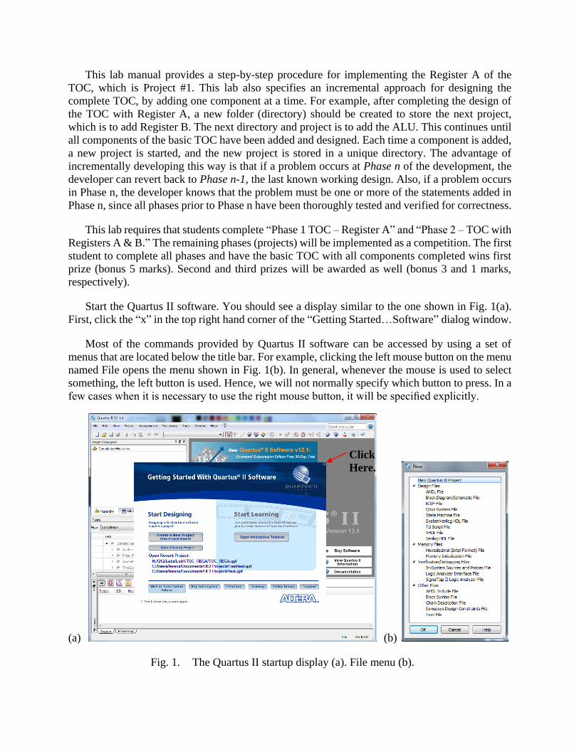
This lab manual provides a step-by-step procedure for implementing the Register A of the
TOC, which is Project #1. This lab also specifies an incremental approach for designing the
complete TOC, by adding one component at a time. For example, after completing the design of
the TOC with Register A, a new folder (directory) should be created to store the next project,
which is to add Register B. The next directory and project is to add the ALU. This continues until
all components of the basic TOC have been added and designed. Each time a component is added,
a new project is started, and the new project is stored in a unique directory. The advantage of
incrementally developing this way is that if a problem occurs at Phase n of the development, the
developer can revert back to Phase n-1, the last known working design. Also, if a problem occurs
in Phase n, the developer knows that the problem must be one or more of the statements added in
Phase n, since all phases prior to Phase n have been thoroughly tested and verified for correctness.
This lab requires that students complete “Phase 1 TOC – Register A” and “Phase 2 – TOC with
Registers A & B.” The remaining phases (projects) will be implemented as a competition. The first
student to complete all phases and have the basic TOC with all components completed wins first
prize (bonus 5 marks). Second and third prizes will be awarded as well (bonus 3 and 1 marks,
respectively).
Start the Quartus II software. You should see a display similar to the one shown in Fig. 1(a).
First, click the “x” in the top right hand corner of the “Getting Started…Software” dialog window.
Most of the commands provided by Quartus II software can be accessed by using a set of
menus that are located below the title bar. For example, clicking the left mouse button on the menu
named File opens the menu shown in Fig. 1(b). In general, whenever the mouse is used to select
something, the left button is used. Hence, we will not normally specify which button to press. In a
few cases when it is necessary to use the right mouse button, it will be specified explicitly.
(a) (b)
Fig. 1. The Quartus II startup display (a). File menu (b).
Click
Here.

For some commands it is necessary to access two or more menus in sequence. We use the
convention Menu1>Menu2>Item to indicate that to select the desired command the user should
first click the left mouse button on Menu1, then within this menu click on Menu2, and then within
Menu2 click on Item. For example, File>Exit uses the mouse to exit from the system. Many
commands can be invoked by clicking on an icon displayed in one of the toolbars. To see the
command associated with an icon, position the mouse over the icon and a tooltip will appear that
displays the command name.
Quartus II Online Help
Quartus II software provides comprehensive online documentation that answers many of the
questions that may arise when using the software. The documentation is accessed from the Help
menu. To get some idea of the extent of documentation provided, it is worthwhile for the reader to
browse through the Help menu. For instance, selecting Help>How to Use Help gives an indication
of what type of help is provided.
The user can quickly search through the Help topics by selecting Help>Search, which opens a
dialog box into which keywords can be entered. Another method, context-sensitive help, is
provided for quickly finding documentation for specific topics. While using most applications,
pressing the F1 function key on the keyboard opens a Help display that shows the commands
available for the application.
2. Starting a New Project
To start working on a new design, we first have to define a new design project. Quartus II
software makes the designer’s task easy by providing support in the form of a Wizard. Create a
new project as follows:
Select File>New Project Wizard to reach the window in Fig. 2, which asks for the name and
directory of the project.
Fig. 2. Creation of the TOC_REGA project.
Set the working directory to be c:\ECE3610\Labs\Lab1\TOC_REGA. The project must have a
name, which should be the same as the top-level module name of the Verilog file that will be
included in the project. Choose TOC_REGA as the name for both the project and the top-level
entity, as shown in Fig. 2. Press Next. Since we have not yet created the directory
Lab1\TOC_REGA, Quartus II software displays the pop-up box asking if it should create the
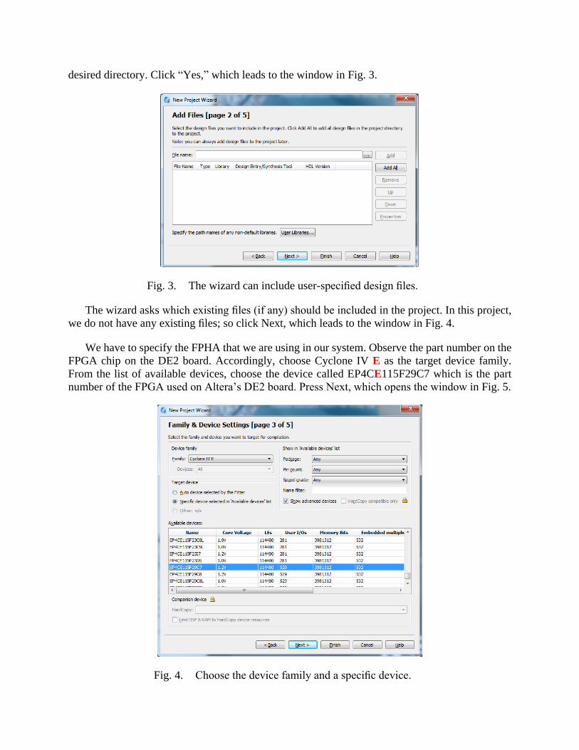
desired directory. Click “Yes,” which leads to the window in Fig. 3.
Fig. 3. The wizard can include user-specified design files.
The wizard asks which existing files (if any) should be included in the project. In this project,
we do not have any existing files; so click Next, which leads to the window in Fig. 4.
We have to specify the FPHA that we are using in our system. Observe the part number on the
FPGA chip on the DE2 board. Accordingly, choose Cyclone IV E as the target device family.
From the list of available devices, choose the device called EP4CE115F29C7 which is the part
number of the FPGA used on Altera’s DE2 board. Press Next, which opens the window in Fig. 5.
Fig. 4. Choose the device family and a specific device.
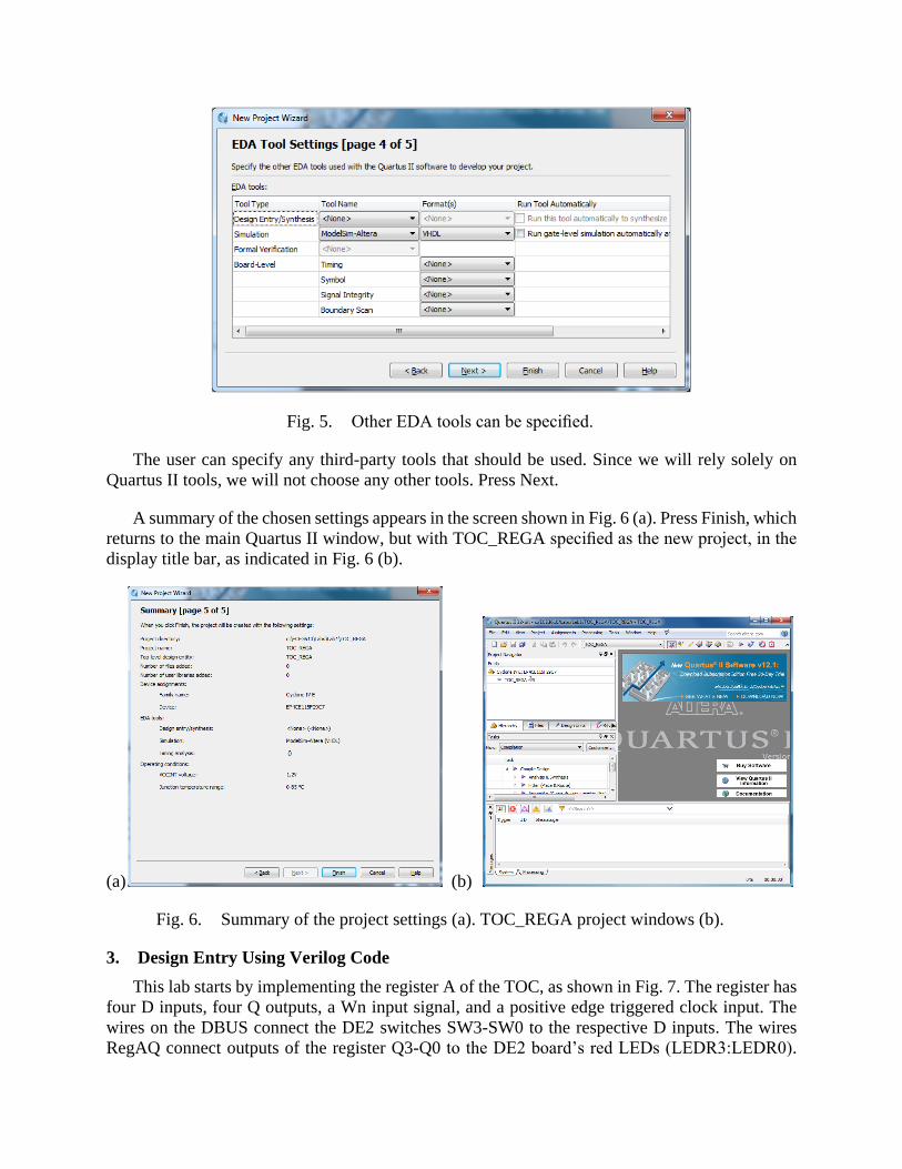
Fig. 5. Other EDA tools can be specified.
The user can specify any third-party tools that should be used. Since we will rely solely on
Quartus II tools, we will not choose any other tools. Press Next.
A summary of the chosen settings appears in the screen shown in Fig. 6 (a). Press Finish, which
returns to the main Quartus II window, but with TOC_REGA specified as the new project, in the
display title bar, as indicated in Fig. 6 (b).
(a) (b)
Fig. 6. Summary of the project settings (a). TOC_REGA project windows (b).
3. Design Entry Using Verilog Code
This lab starts by implementing the register A of the TOC, as shown in Fig. 7. The register has
four D inputs, four Q outputs, a Wn input signal, and a positive edge triggered clock input. The
wires on the DBUS connect the DE2 switches SW3-SW0 to the respective D inputs. The wires
RegAQ connect outputs of the register Q3-Q0 to the DE2 board’s red LEDs (LEDR3:LEDR0).
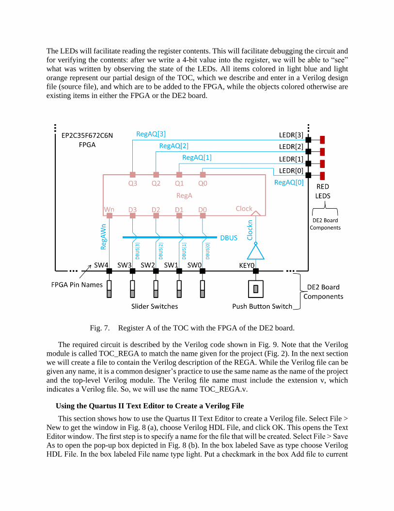
The LEDs will facilitate reading the register contents. This will facilitate debugging the circuit and
for verifying the contents: after we write a 4-bit value into the register, we will be able to “see”
what was written by observing the state of the LEDs. All items colored in light blue and light
orange represent our partial design of the TOC, which we describe and enter in a Verilog design
file (source file), and which are to be added to the FPGA, while the objects colored otherwise are
existing items in either the FPGA or the DE2 board.
Fig. 7. Register A of the TOC with the FPGA of the DE2 board.
The required circuit is described by the Verilog code shown in Fig. 9. Note that the Verilog
module is called TOC_REGA to match the name given for the project (Fig. 2). In the next section
we will create a file to contain the Verilog description of the REGA. While the Verilog file can be
given any name, it is a common designer’s practice to use the same name as the name of the project
and the top-level Verilog module. The Verilog file name must include the extension v, which
indicates a Verilog file. So, we will use the name TOC_REGA.v.
Using the Quartus II Text Editor to Create a Verilog File
This section shows how to use the Quartus II Text Editor to create a Verilog file. Select File >
New to get the window in Fig. 8 (a), choose Verilog HDL File, and click OK. This opens the Text
Editor window. The first step is to specify a name for the file that will be created. Select File > Save
As to open the pop-up box depicted in Fig. 8 (b). In the box labeled Save as type choose Verilog
HDL File. In the box labeled File name type light. Put a checkmark in the box Add file to current

project. Click Save, which puts the file into the directory Lab1\TOC_REGA.
(a) (b)
Fig. 8. Choose to create a Verilog file (a). Saving the file (b).
Maximize the Text Editor window and enter the following Verilog statements. Save the file by
typing File > Save, or by typing the shortcut Ctrl-s.
module TOC_REGA (SW, KEY, LEDR);
input [17:0] SW;
input [3:0] KEY;
output [17:0] LEDR;
wire [3:0] DBUS, RegAQ;
wire RegAWn, Clock, Clockn;
assign LEDR [3:0] = RegAQ [3:0];
assign Clockn = !Clock;
assign RegAWn = SW[4], Clock = KEY[0];
assign DBUS[3] = SW[3], DBUS[2] = SW[2];
assign DBUS[1] = SW[1], DBUS[0] = SW[0];
reg4 AReg (DBUS, RegAWn, Clockn, RegAQ);
endmodule
module reg4 (D, Wn, Clock, Q);
input [3:0] D;
input Clock, Wn;
output reg [3:0] Q;
always @ (posedge Clock)
if (Wn==0)
Q <= D;
endmodule

The result should be as shown in Fig. 9. Click on the Files tab in the left side panel to view the
list of files in the project (only one in this case, TOC_REGA.v).
Most of the commands available in the Text Editor are self-explanatory. Text is entered at the
insertion point, which is indicated by a thin vertical line. The insertion point can be moved either
by using the keyboard arrow keys or by using the mouse. Two features of the Text Editor are
especially convenient for typing Verilog code. First, the editor can display different types of
Verilog statements in different colors, which is the default choice. Second, the editor can
automatically indent the text on a new line so that it matches the previous line. Such options can be
controlled by the settings in Tools > Options > Text Editor.
Fig. 9. Quartus II window with the TOC_REGA design.
Adding Design Files to a Project
As we indicated when discussing Fig. 3, you can tell Quartus II software which design files it
should use as part of the current project. To see the list of files already included in the light project,
select Assignments > Settings, which leads to the window in Fig. 10. As indicated on the left side
of the figure, click on the item Files. An alternative way of making this selection is to choose
Project > Add/Remove Files in Project.
Recall that we checked the box labeled “Add file to current project” when we created the
TOC_REGA.v file, and so it will be listed in the window in Fig. 10 (a).

If you want to add files to a project, select Project > Add/”Remove Files in Project”. Then,
click on the ... button in Fig. 10 (a) to get the pop-up window in Fig. 10 (b). (Note: the files you
want to add should be previously placed in the current project directory.) Select the file you want
to add and click Open. The selected file is now indicated in the Files window. Finally, click OK to
include the file in the project.
(a) (b)
Fig. 10. Settings window (a). Adding file to project (b).
4. Pin Assignment
During the compilation process, the Quartus II Compiler would be free to choose any pins on
the selected FPGA to connect to the input and output variables that were specified in the Verilog
top-level source file being compiled. The compiler will connect the inputs and outputs specified in
the top-level design file (SW, KEY, and LEDR) to arbitrary I/O pins on the FPGA chip if not
instructed otherwise. The DE2 board has hardwired connections between certain FPGA pins and
other components on the board. For example, the slider switches (SW17:SW0), push button
switches (KEY3:KEY0), and the red LEDs (LEDR17:LEDR0) on the board are connected to
certain pins of the FPGA. To use these input and output devices (i.e., switches and LEDs) in our
design, we need to do two things:
(i) Assign names to the FPGA pins to which these input and output devices are connected, and
(ii) Declare the names of the inputs and outputs in our Verilog source file with the same names
as we had assigned in step (i).
For example, the slider switches SW0 and SW1 are connected to pins PIN_AB28 and
PIN_AC28 of the FPGA chip. To use these devices in our design, we would need to assign names
to these pins, and then use those same names in our Verilog source file.
The easiest way to assign names to the pins which connect to input and output devices is to
import a file, called a “pin assignment file,” that already assigns names to the pins and indicates the
I/O device to which the pin is connected on the DE2 board. Using the OS and a Text Editor, open
the file: “C:\altera\DE2_115.qsf” and browse its contents.
To import the pin assignments into our design, select: Assignments Import Assignments
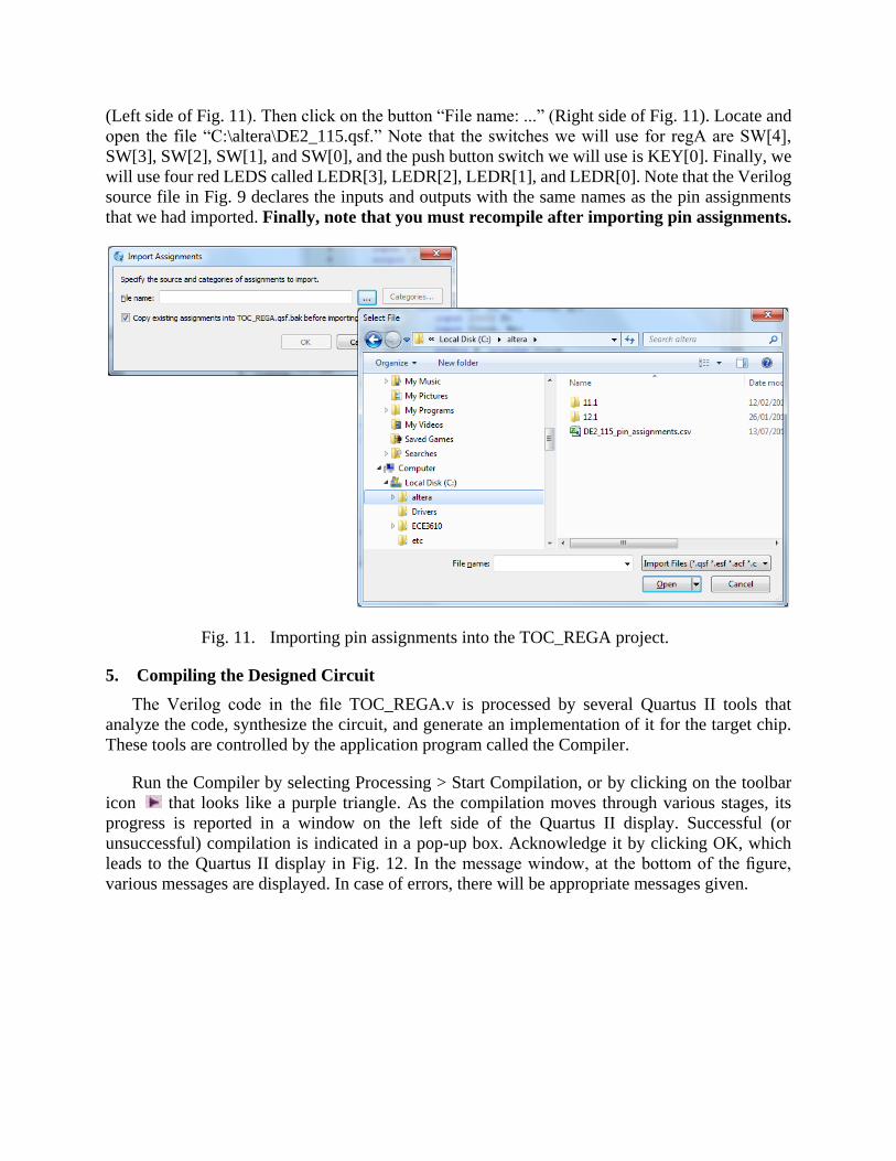
(Left side of Fig. 11). Then click on the button “File name: ...” (Right side of Fig. 11). Locate and
open the file “C:\altera\DE2_115.qsf.” Note that the switches we will use for regA are SW[4],
SW[3], SW[2], SW[1], and SW[0], and the push button switch we will use is KEY[0]. Finally, we
will use four red LEDS called LEDR[3], LEDR[2], LEDR[1], and LEDR[0]. Note that the Verilog
source file in Fig. 9 declares the inputs and outputs with the same names as the pin assignments
that we had imported. Finally, note that you must recompile after importing pin assignments.
Fig. 11. Importing pin assignments into the TOC_REGA project.
5. Compiling the Designed Circuit
The Verilog code in the file TOC_REGA.v is processed by several Quartus II tools that
analyze the code, synthesize the circuit, and generate an implementation of it for the target chip.
These tools are controlled by the application program called the Compiler.
Run the Compiler by selecting Processing > Start Compilation, or by clicking on the toolbar
icon that looks like a purple triangle. As the compilation moves through various stages, its
progress is reported in a window on the left side of the Quartus II display. Successful (or
unsuccessful) compilation is indicated in a pop-up box. Acknowledge it by clicking OK, which
leads to the Quartus II display in Fig. 12. In the message window, at the bottom of the figure,
various messages are displayed. In case of errors, there will be appropriate messages given.
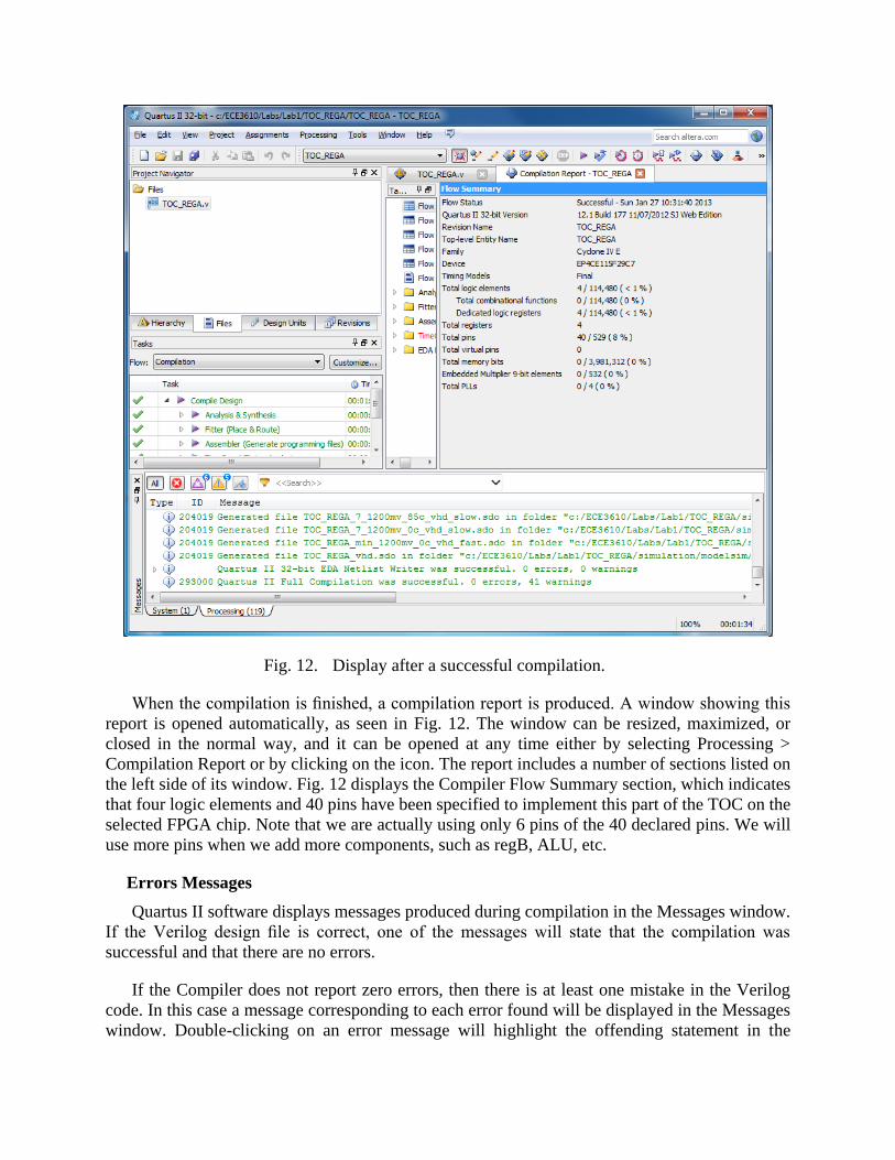
Fig. 12. Display after a successful compilation.
When the compilation is finished, a compilation report is produced. A window showing this
report is opened automatically, as seen in Fig. 12. The window can be resized, maximized, or
closed in the normal way, and it can be opened at any time either by selecting Processing >
Compilation Report or by clicking on the icon. The report includes a number of sections listed on
the left side of its window. Fig. 12 displays the Compiler Flow Summary section, which indicates
that four logic elements and 40 pins have been specified to implement this part of the TOC on the
selected FPGA chip. Note that we are actually using only 6 pins of the 40 declared pins. We will
use more pins when we add more components, such as regB, ALU, etc.
Errors Messages
Quartus II software displays messages produced during compilation in the Messages window.
If the Verilog design file is correct, one of the messages will state that the compilation was
successful and that there are no errors.
If the Compiler does not report zero errors, then there is at least one mistake in the Verilog
code. In this case a message corresponding to each error found will be displayed in the Messages
window. Double-clicking on an error message will highlight the offending statement in the
Verilog code in the Text Editor window. Similarly, the Compiler may display some warning
messages. Their details can be explored in the same way as in the case of error messages. The user
can obtain more information about a specific error or warning message by selecting the message
and pressing the F1 function key.
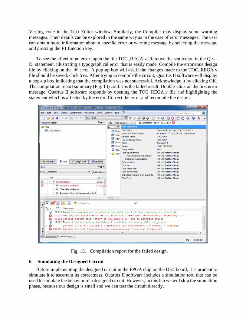
To see the effect of an error, open the file TOC_REGA.v. Remove the semicolon in the Q <=
D; statement, illustrating a typographical error that is easily made. Compile the erroneous design
file by clicking on the icon. A pop-up box will ask if the changes made to the TOC_REGA.v
file should be saved; click Yes. After trying to compile the circuit, Quartus II software will display
a pop-up box indicating that the compilation was not successful. Acknowledge it by clicking OK.
The compilation report summary (Fig. 13) confirms the failed result. Double-click on the first error
message. Quartus II software responds by opening the TOC_REGA.v file and highlighting the
statement which is affected by the error. Correct the error and recompile the design.
Fig. 13. Compilation report for the failed design.
6. Simulating the Designed Circuit
Before implementing the designed circuit in the FPGA chip on the DE2 board, it is prudent to
simulate it to ascertain its correctness. Quartus II software includes a simulation tool that can be
used to simulate the behavior of a designed circuit. However, in this lab we will skip the simulation
phase, because our design is small and we can test the circuit directly.
7. Programming and Configuring the FPGA Device
The FPGA device must be programmed and configured to implement the designed circuit. The
required configuration file is generated by the Quartus II Compiler’s Assembler module. Altera’s
DE2 board allows the configuration to be done in two different ways, known as JTAG and AS
modes. The configuration data is transferred from the host computer (which runs the Quartus II
software) to the board by means of a cable that connects a USB port on the host computer to the
leftmost USB connector on the board (the one labeled “Blaster.”)
In the JTAG mode, the configuration data is loaded directly into the FPGA device. The
acronym JTAG stands for Joint Test Action Group. This group defined a simple way for testing
digital circuits and loading data into them, which became an IEEE standard. If the FPGA is
configured in this manner, it will retain its configuration as long as the power remains turned on.
The configuration information is lost when the power is turned off.
The second possibility is to use the Active Serial (AS) mode. In this case, a configuration
device that includes some flash memory is used to store the configuration data. Quartus II software
places the configuration data into the configuration device on the DE2 board. Then, this data is
loaded into the FPGA upon power-up or reconfiguration. Thus, the FPGA need not be configured
by the Quartus II software if the power is turned off and on. The choice between the two modes is
made by the RUN/PROG switch on the DE2 board. The RUN position selects the JTAG mode,
while the PROG position selects the AS mode.
JTAG Programming
The programming and configuration task is performed as follows. Flip the RUN/PROG switch
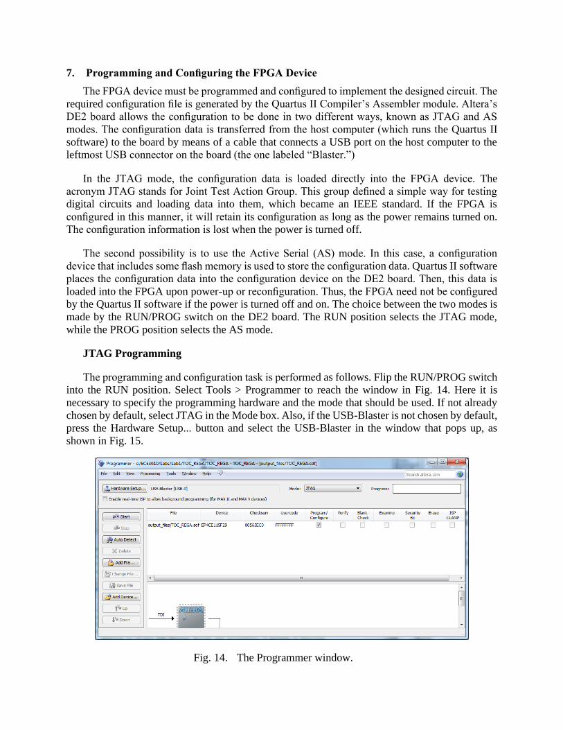
into the RUN position. Select Tools > Programmer to reach the window in Fig. 14. Here it is
necessary to specify the programming hardware and the mode that should be used. If not already
chosen by default, select JTAG in the Mode box. Also, if the USB-Blaster is not chosen by default,
press the Hardware Setup... button and select the USB-Blaster in the window that pops up, as
shown in Fig. 15.
Fig. 14. The Programmer window.

Ensure that the associated configuration file TOC_REGA.sof is listed in the window in Fig. 14.
If the file is not already listed, then click “Add File” or “Change File” and browse to your project
folder and select the *.sof file; in this case it is in the TOC_REGA folder. This is a binary file
produced by the Compiler’s Assembler module, which contains the data needed to configure the
FPGA device. The extension .sof stands for SRAM Object File. Note also that the device selected
is EP4CE115F29C7, which is the FPGA device used on the DE2 board. Click to place a check
mark in the Program/Configure check box, as shown in Fig. 14.
Fig. 15. The Hardware Setup window.
Now, press Start in the window in Fig. 14. An LED on the board will light up when the
configuration data has been downloaded successfully. If you see an error reported by Quartus II
software indicating that programming failed, and then check to ensure that the board is properly
powered on and the USB cable is connected to the “Blaster” connector on the DE2 Board. Close
the Programmer window after successful programming.
8. Testing the Designed Circuit
Having downloaded the configuration data into the FPGA device, you can now test the
implemented circuit. Perform the following test cases and answer the following questions:
1. Write the data ‘1010’ by setting up the switches SW3:SW0 as 1010. Then, make SW4 = 0
(SW4 is connected to the register’s Wn control signal, which, when low, will enable
writing to the register). Next, press the push button switch (KEY0) down. As soon as
KEY0 (i.e., Clock) is pushed down, you should see LEDR[3] and LEDR[1] light up. These
LEDs are connected to the outputs of the register. Then, release the Clock and observe
what happens.
2. Do the same test as Test Case 1, except while holding KEY0 push button down, change the
data at switches SW3:SW0 to any other value other than 1010. Explain why the LEDR do

not change.
3. Do the same test as Test Case 1 with other instances of data, such as ‘1111’ and ‘0111’.
4. Do the same test as Test Case 1, except make SW4 = 1, and observe and explain what
happens.
5. Draw a timing diagram to show the procedure for writing to the register. Explain the
procedure (if any) for reading from the register.
9. Adding Register B
Add Register B using the following procedure:
1. Close all projects.
2. Start the New Project Wizard to create a new project; name it TOC_REGAB. Place the
project in directory Lab1\TOC_REGAB. Press Next to create the directory.
3. Using the OS, copy the file TOC_REGA.v (Verilog file) from directory Lab1\TOC_REGA
to directory Lab1\TOC_REGAB. Rename the file to TOC_REGAB.v
4. Add the TOC_REGAB.v file to your new project.
5. Change the top-level module name to TOC_REGAB
6. Add your design of the Register B to the Verilog file TOC_REGAB.v, adhering to the
following constraints: (i) Connect the Q outputs of the Register B to the LEDs
(LEDR7:LEDR4). (ii) Use SW[5] to connect and control the Wn signal of Register B.
7. Compile and upload your design to the FPGA.
8. Test and answer the same test case and questions as for register A, except perform the tests
on Register B.
OPTIONAL COMPETITION ADDITIONS
The following additions are optional and for competition.
10. Adding ALU
Add an ALU using the following procedure:
1. Close any existing project.
2. Start the New Project Wizard to create a new project; name it TOC_REGAB_ALU. Place
the project in directory Lab1\TOC_REGAB_ALU. Press Next to create the directory.
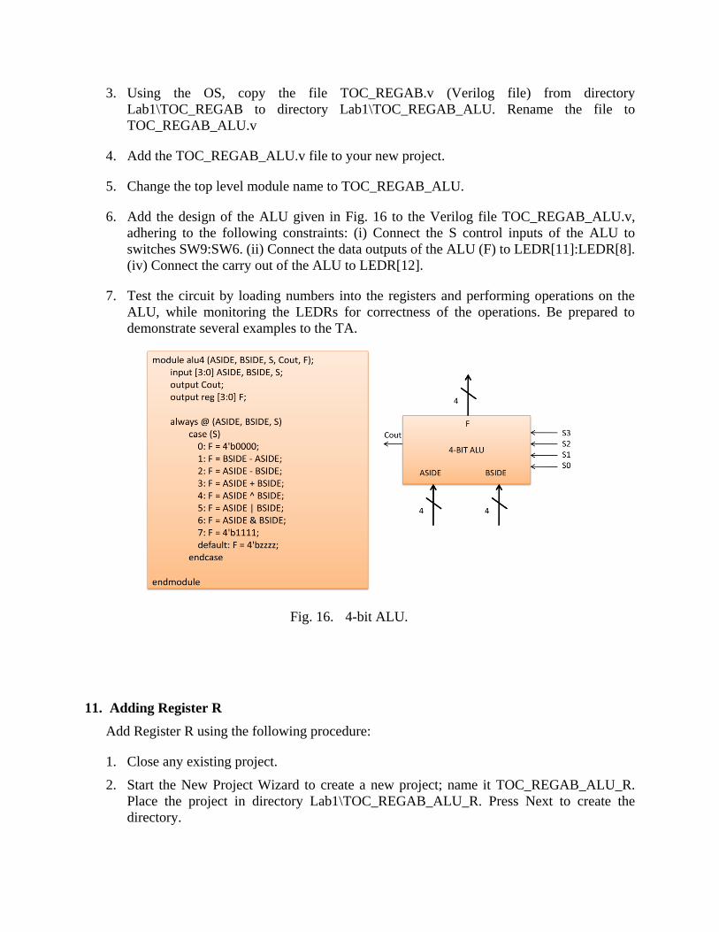
3. Using the OS, copy the file TOC_REGAB.v (Verilog file) from directory
Lab1\TOC_REGAB to directory Lab1\TOC_REGAB_ALU. Rename the file to
TOC_REGAB_ALU.v
4. Add the TOC_REGAB_ALU.v file to your new project.
5. Change the top level module name to TOC_REGAB_ALU.
6. Add the design of the ALU given in Fig. 16 to the Verilog file TOC_REGAB_ALU.v,
adhering to the following constraints: (i) Connect the S control inputs of the ALU to
switches SW9:SW6. (ii) Connect the data outputs of the ALU (F) to LEDR[11]:LEDR[8].
(iv) Connect the carry out of the ALU to LEDR[12].
7. Test the circuit by loading numbers into the registers and performing operations on the
ALU, while monitoring the LEDRs for correctness of the operations. Be prepared to
demonstrate several examples to the TA.
Fig. 16. 4-bit ALU.
11. Adding Register R
Add Register R using the following procedure:
1. Close any existing project.
2. Start the New Project Wizard to create a new project; name it TOC_REGAB_ALU_R.
Place the project in directory Lab1\TOC_REGAB_ALU_R. Press Next to create the
directory.

3. Using the OS, copy the file TOC_REGAB_ALU.v (Verilog file) from directory
Lab1\TOC_REGAB_ALU to directory Lab1\TOC_REGAB_ALU_R. Rename the file to
TOC_REGAB_ALU_R.v
4. Add the TOC_REGAB_ALU_R.v file to your new project.
5. Change the top level module name to TOC_REGAB_ALU_R.
6. Add your design of the Register R to the Verilog file TOC_REGAB_ALU_R.v, adhering
to the following constraints: (i) Connect the Q outputs of the Register R to the LEDs
(LEDR16:LEDR13). (ii) Use SW[10] to connect and control the Wn signal of Register R.
7. Compile and upload your design to the FPGA.
8. Test the circuit by loading numbers into the registers A & B and performing operations on
the ALU, while monitoring the LEDR16:LEDR13 for correctness of the operations.
Observe that Register R performs a write operation only when its Wn is low and its Clock
undergoes a positive transition. Observe that the positive transition is implemented by
returning the push button switch KEY0 back up. Demonstrate several examples to the TA.
12. Adding BCD 2 Seven Segment Decoder
Add a BCD to seven-segment decoder using the following procedure:
1. Close any existing project.
2. Start the New Project Wizard to create a new project; name it
TOC_REGAB_ALU_R_BCD7. Place the project in directory
Lab1\TOC_REGAB_ALU_R_BCD7. Press Next to create the directory.
3. Using the OS, copy the file TOC_REGAB_ALU_R.v (Verilog file) from directory
Lab1\TOC_REGAB_ALU to directory Lab1\TOC_REGAB_ALU_R_BCD7. Rename the
file to TOC_REGAB_ALU_R_BCD7.v
4. Add the TOC_REGAB_ALU_R_BCD7.v file to your new project.
5. Change the top level module name to TOC_REGAB_ALU_R_BCD7.
6. Add your design of the BCD7 to the Verilog file TOC_REGAB_ALU_R_BCD7.v,
adhering to the following constraints: (i) Connect the 7 outputs of the BCD to the seven
inputs of the seven-segment display HEX0.
7. Compile and upload your design to the FPGA.
8. Test the TOC circuit by loading numbers into the registers A & B and performing
operations on the ALU, while monitoring the HEX0 display for correctness of the
operations. Be prepared to demonstrate several examples to the TA.