ece 342 electronic circuits lecture 30 operational
TRANSCRIPT

ECE 342 – Jose Schutt‐Aine 1
ECE 342Electronic Circuits
Lecture 30Operational Amplifiers ‐ 1
Jose E. Schutt-AineElectrical & Computer Engineering
University of [email protected]

ECE 342 – Jose Schutt‐Aine 2
Operational Amplifiers
General terminal configuration with bias
• Universal importance (e.g. amplification from microphone to loudspeakers)

ECE 342 – Jose Schutt‐Aine 3
Common configuration with bias implied but not shown
Operational Amplifiers
2 1( )outv A v v
Gain=A
• Signaling1. Differential input stage2. Difference between input is amplified

ECE 342 – Jose Schutt‐Aine 4
2. Zero output impedance
Operational Amplifiers
Also, op amps are dc (or direct coupled) amplifiers since they are expected to amplify signals with frequency as low as DC.
1. Infinite input impedance
• Ideal Op Amp
4. Infinite CMRR or zero common-mode gain
3. Infinite open-loop gain Ainf
5. Infinite bandwidth

ECE 342 – Jose Schutt‐Aine 5
Differential & Common-Mode Signals- Differential input signal vID=v2-v1- Common-mode input signal vICm=0.5(v1+v2)
1 2ID
ICmvv v
2 2ID
ICmvv v

ECE 342 – Jose Schutt‐Aine 6
Ideally, vICM should be zero to achieve high CMRR.
• Amplifier will amplify the difference between the two input signals
Operational Amplifiers

ECE 342 – Jose Schutt‐Aine 7
Practical ConsiderationsThe output voltage swing of an op amp is limited by the DC power supply. Since op amp can exhibit high gain, power supply voltage fluctuations must be minimized use decoupling capacitors from power supply

ECE 342 – Jose Schutt‐Aine 8
Inverting Configuration
We introduce RF (or R2) to reduce gain (from inf)
• When RF is connected to terminal 1, we talk about negative feedback. If RF is tied to terminal 2, we have positive feedback
Terminal 2 is tied to ground

ECE 342 – Jose Schutt‐Aine 9
Inverting Configuration
Need to evaluate vo/vI
Assume ideal Op-Amp
2 1( ) 0ov v vA Since gain is infinite:
v1 is virtual ground
1 2, 0Thus v v
11
1 1
I Iv v viR R
Note: A is open-loop gain

ECE 342 – Jose Schutt‐Aine 10
Since input impedance of OP amp is infinite, current through RF is i1
11
Ivi iR
1
1
0o o I
F F
v v v viR R R
1 1
o I Fo I
F
v v Rv vR R R
Inverting Configuration

ECE 342 – Jose Schutt‐Aine 11
1
o F
I
v R Gv R
Closed-Loop gain
Observe that the closed-loop gain is the ratio of external components we can make the closed-loop as accurate as we want. Gain is smaller but more accurate.
Inverting Configuration

ECE 342 – Jose Schutt‐Aine 12
2 1 1 /o ov v A v v v A
We assumed that the OP-amp was ideal. If we assume that the gain A is finite = A
Inverting Configuration
11 1
( / ) /in o in ov v A v v AiR R

ECE 342 – Jose Schutt‐Aine 13
1
/i o Fo oo F
v v A Rv vv iRA A R
Still assume infinite input impedance
Inverting Configuration
1
1 1
/1 / / 1
o F F
I F F
v R R ARGv R R A R A R
1 1F
F
ARGR A R
Closed-loop gain
forinverting configuration

ECE 342 – Jose Schutt‐Aine 14
11
1
/
/
oR
oo
v A RvR vi v AG
The reflected impedance of RF is given by
Inverting Configuration
1
1R
RR AG
since 11 (1 )
F
A R AG R
1F
RRR
A
small

ECE 342 – Jose Schutt‐Aine 15
Inverting Configuration
Since the reflected impedance is so small, v1 is thus very small and the inverting terminal is said to be a virtual ground in this configuration
1
, FRas A GR
We see that
, 0Ras A R Note: To minimize the closed-loop gain (G) on the value of the open-loop gain (A), make 1+RF/R1 << A

ECE 342 – Jose Schutt‐Aine 16
11 1/I I
iI
v vR Ri v R
Input and Output Impedances
‐ If high gain is required, input impedance will be low‐Output impedance is zero
Inverting Configuration

ECE 342 – Jose Schutt‐Aine 17
Find closed-loop gain for A=103, A=104 and A=105
assuming R1=1 k and RF=100 k. Assuming vI=0.1 V, find v1.
Example
A |G| v1
Using formulas
Note: Since output of inverting configuration is at terminal of VCVS, output impedance of closed-loop amp is zero.
103 90.83 -9.08 mV104 99.00 -0.99 mV105 99.90 -0.1 mV

ECE 342 – Jose Schutt‐Aine 18
Non-Inverting Configuration
0oID
vvA
Assume gain is
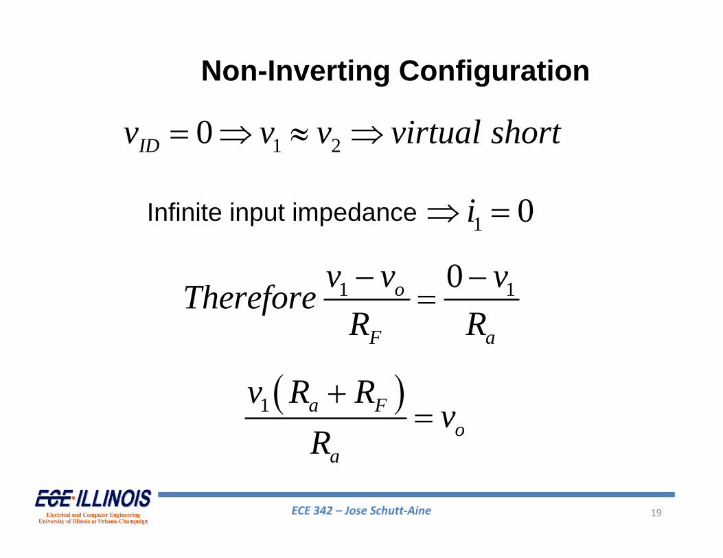
ECE 342 – Jose Schutt‐Aine 19
1 20 IDv v v virtual short
Infinite input impedance
Non-Inverting Configuration
1 0i
1 10o
F a
v v vThereforeR R
1 a Fo
a
v R Rv
R

ECE 342 – Jose Schutt‐Aine 20
Virtual short
Non-Inverting Configuration
2 1Iv v v
a FI o
a
R Rv v
R
1o F
I a
v RGv R
1 F
a
RGR

ECE 342 – Jose Schutt‐Aine 21
The Buffer Stage
0, 1 1FF
a
RIf R GR
Although voltage gain is low, current gain can be quite high. Buffer stage can be used to interface between processors and switches.

ECE 342 – Jose Schutt‐Aine 22
The Voltage Follower
‐ Unity gain amplifier‐ 100% negative feedback
inR
0outR