ece 2300 digital logic & computer organization · digital logic & computer organization ....
TRANSCRIPT

Lecture 4:
Spring 2018
CMOS Logic
1
ECE 2300Digital Logic & Computer Organization

Lecture 4: 2
NAND Logic Gate
X Y
(X•Y)’
Y
X
Y’
X’ X’+Y’
Using De Morgan’s Law: (X•Y)’ = X’+Y’
Also a NAND
NAND =
=
We can build circuits from NAND only!

Lecture 4: 3
• NOT
• AND
• OR
We Can Build Circuits from NAND Only!

Lecture 4:
NOR Logic Gate
4
X Y
X+Y (X+Y)’
Using De Morgan’s Law: (X+Y)’ = X’•Y’
X
Y
X’
Y’
X’•Y’
NOR
Also a NOR
=
=
We can build circuits from NOR only!

Lecture 4:
Sum-of-Products Revisited
5
AND-OR
NAND-NAND

Lecture 4:
Product-of-Sums Revisited
6
OR-AND
NOR-NOR

Lecture 4: 7
A Little Bit of History
IEEE SOLID-STATE CIRCUITS MAGAZINE SUMMER 20 10 33
circuit, logic, and architecture. At each abstraction level, the verifica-tion problem was typically the most painful; hence it was addressed first. The synthesis problem at that level was addressed much later.
This article is the story of the coevolution of design methodolo-gies, practices, and CAD tools in Intel’s design environment as it coped with increasing complexity in the turbulent 1980s and up through recent years. It is interesting to note that at the beginning of this process the engineering culture was advo-cating a tall, thin design. Nowadays, very large scale integration (VLSI) engineers are highly specialized in different areas of the design disci-pline, where specialized tools are used in each area. This is analogous to the restructuring of the whole computer industry from vertical to horizontal.
In the 1980s, the CAD industry itself was nascent at best. While some areas like schematic or layout entry had solid commercial offer-ings, the rapidly evolving complex-ity of this young industry meant there could be little hope from commercial tool offerings. There-fore most tools emerged from inter-nal development, external university research, or often a coevolving blend of internal work with external tools and research. While there were a number of corporate-university relationships at that time, none was as prolific as that of Intel with the University of California, Berkeley. In particular, Alberto Sangiovanni-Vincentelli and his collaborative research team, which consisted of Robert Brayton, Richard Newton, and many graduate students, had devel-oped a strong partnership with Intel and its microprocessor teams. This long partnership with Intel stands as one of the most fruitful relation-ships in EDA, bringing fundamental breakthroughs in multiple elements of microprocessor logic, synthesis, and layout. Many of these early suc-cesses resulted in enormous ben-efits to Intel and eventually made
their way into the EDA industry as key enablers of many EDA tools and today’s fabless ASIC/SOC semicon-ductor industry.
Design Environment for the Early X86 Processors
Inherited Tools from Memory ChipsIntel’s initial design environment was formed to serve the needs of memory chips. During the 1970s, the primary CAD tools were layout capture and verification tools, used by draftsmen to generate and check mask layouts. These tools were put in place because the layouts were already too complicated to develop and maintain solely on paper or Mylar. Polygon-based layout repre-sentations therefore had to be stored
and handled by computerized tools, initially on dedicated systems such as the Calma or Applicon.
Engineers were doing circuit and logic designs at the transistor level, usually by hand, producing hand-drawn schematics at the transistor level for the layout designers. The engineers did most of their design work using pencil and paper, but they also had circuit simulation tools derived from the industry-standard SPICE [3] program. SPICE
originated in Don Pederson’s group at Berkeley and later on was refined by Richard Newton, Alberto, and their students (Intel’s version was known as ISPEC). It was possible to simulate and check logic behavior and timing waveforms for small cir-cuits that incorporated up to a few hundred transistors.
As Intel started designing logic products, including the first micro-processors (the Intel 4004, 8008, and 8080), design engineers inher-ited all of those tools and methods, which had initially been conceived for memory chip design. Some engi-neers preferred to perform logic design using gate-level schemat-ics, but this generated some resis-tance from the layout designers. They were familiar with transistor
representations, which directly matched the layout. Translating logic gate symbols into transistor struc-tures was not a trivial task because the early microprocessors and numeric coprocessors (8087, 80387) were designed in NMOS technology. Circuit operation relied on device strength ratios, so each gate symbol had to be accompanied by specific transistor sizes. In addition, the pre-vailing design style supported many complex gate pull-down devices,
TABLE 1. INTEL PROCESSORS, 1971–1993.
PROCESSOR INTRO DATE PROCESS TRANSISTORS FREQUENCY
4004 1971 10 mm 2,300 108 KHz
8080 1974 6 mm 6,000 2 MHz
8086 1978 3 mm 29,000 10 MHz
80286 1982 1.5 mm 134,000 12 MHz
80386 1985 1.5 mm 275,000 16 MHz
Intel 486 DX 1989 1 mm 1.2 M 33 MHz
Pentium 1993 0.8 mm 3.1 M 60 MHz
This article is the story of the coevolution of design methodologies, practices, and CAD tools in Intel’s design environment as it coped with increasing complexity in the turbulent 1980s and up through recent years.
Source: Patrick Gelsinger, Desmond Kirkpatrick, Avinoam Kolodny, and Gadi Singer. "Such a CAD!." IEEE Solid-State Circuits Magazine, 2010.
• Transistors – Invented by John Bardeen, Walter Brattain, and William
Shockley at Bell Labs in 1947 • Integrated circuits
– Independently developed by Jack Kilby (at TI) and Robert Noyce (at Fairchild) in the 1950s
– Noyce and Gordon Moore founded Intel in 1968

Lecture 4: 8
Era of Billion-Transistor Chips
Oracle SPARC M7 ~10B transistors
Intel Haswell-EP Xeon E5 ~7B transistors
Apple A11 ~4B transistors
Intel/Altera Stratix 10~30B transistors
NVIDIA V100 Pascal ~21B transistors
IBM Power9 ~8B transistors

Lecture 4: 9
MOS Transistors • Metal-Oxide Semiconductor Field-Effect
Transistors (MOSFETS) – MOS transistors for short
• Extreme changes in resistance (0 to ∞) make
transistors act like switches
A 3-terminal device controlled by the gate voltage that acts like a switch
gate source
drain
Carriers (holes or
electrons) VIN
L2 – CMOS 9 ENGRD 2300
Our Switches: MOS Transistors • MOSFETs
– Metal-Oxide Semiconductor Field-Effect Transistors – Shortened to MOS transistors
gate
source
Voltage-controlled resistance (switch)
• Extreme changes in resistance (0 to ∞) make transistors act like switches
drain
Carriers (holes or electrons) W
L
gate
drain
source

Lecture 4: 10
NOT Gate Input & Output Voltages
• When the input voltage is low, the output should be connected to the voltage supply (e.g., VDD, VCC)
• When the input voltage is high, the output should be connected to ground (i.e., GND)
A Y
0 1
1 0
A Y
0V 5V
5V 0V
A Y
L H
H L

Lecture 4: 11
NOT Using Switches A Y
0 1
1 0
A Y
0V 5V
5V 0V
A Y
L H
H L
• Can build a NOT using two types of switches – Type 1: Closed when input = 0,
open when input = 1 – Type 2: Closed when input = 1,
open when input = 0

Lecture 4: 12
NAND Using Switches
H L L
Y B A
Output Inputs 5V
A = L
B = L
Y = H
Type 1: closed
Type 2: open
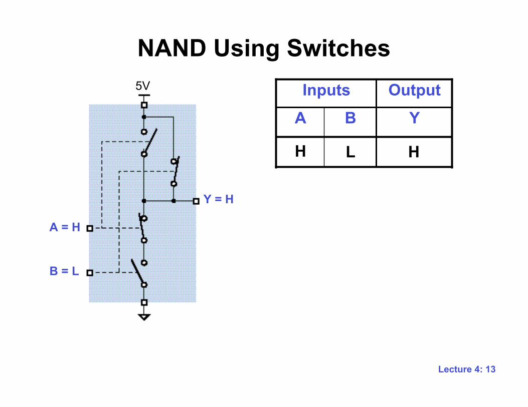
Lecture 4: 13
NAND Using Switches
H
Y B A
Output Inputs
L H
5V
A = H
B = L
Y = H

Lecture 4: 14
NAND Using Switches 5V
A = H
B = H
Y = L
H
Y B A
Output Inputs
H L

Lecture 4: 15
• Current flows when ON (conducting) • No current flows when OFF (not conducting)
• Type 1 and Type 2 switches
PMOS or
p-channel
NMOS or
n-channel
Bubble: LOW closes the switch
S
G
D
D
G
S
MOS Transistors
Type 1 Type 2
G: Gate; S: Source; D: Drain

Lecture 4: 16
MOS Transistors
PMOS and NMOS have
complementary properties
• PMOS – Closed when input is low [1] – Open when input is high – Passes a good one (but a poor
zero) [2] • NMOS
– Closed when input is high [1] – Open when input is low – Passes a good zero (but a poor
one) [2]
D
S
G
G
D
S
[1] In both cases, the voltage difference between the gate and source must exceed certain threshold voltage before the the transistor starts having any effect [2] Optional reading: vlsimsee.blogspot.com/2013/05/why-cant-nmos-pass-1-and-pmos-pass-0.html

Lecture 4: 17
CMOS Logic Gates • Complementary MOS (CMOS)
– CMOS dominates the digital IC market
• Uses both NMOS and PMOS devices such that there is no direct supply-ground path – Dissipates little power when the
inputs don’t change
• Our focus: Static CMOS gates – Other types exist as well (pseudo-
NMOS, domino, ...)
VDD
P
N
…
…
GND

Lecture 4: 18
CMOS Inverter
Vin
VDD
T1
T2
Vin is high T1 is off T2 is on Vout is low
Vin is low T1 is on T2 is off Vout is high
S
S
D
D G
G
Vout
Vin Vout

Lecture 4: 19
CMOS NAND Gate

Lecture 4: 20
3 Input CMOS NAND Gate
An n-input NAND uses 2n transistors

Lecture 4: 21
Exercise: A “Mystery” Gate
(1) Fill out the missing entries in the above table (on/off); (2) Identify the logic gate that is implemented by the CMOS network

Lecture 4: 22
2-Input AND Gate • CMOS gates produce inherent inversion • Need to add an inverter to a 2-Input NAND to
form AND gate

Lecture 4: 23
Structure of Transistor Networks • Two complementary
networks: – A pull-up network composed
of PMOS, with sources tied to voltage supply
– A pull-down network composed of NMOS, with sources tied to ground
– Equal number of NMOS and PMOS transistors
Pull-up network
Pull-down network

Lecture 4: 24
Structure of Transistor Networks • The pull-up and pull-down
networks are always duals
• To construct the dual of a network: – Exchange NMOS for PMOS
(and vice versa) – Exchange series subnets for
parallel subnets (and vice versa)
• This transformation applies to hierarchical structures
Parallel subnet
Series subnet

Lecture 4: 25
Duality of Parallel/Series Subnets
Pull-down series subnet F pulls down to 0 when A and B are high => F = (A•B)’
Pull-up parallel subnet F pulls up to 1 when A or B is low => F = A’+B’ = (A•B)’
Pull-down parallel subnet F pulls down to 0 when A or B is high => F = (A+B)’
Pull-up series subnet F pulls up to 1 when A and B are low => F = A’B’ = (A+B)’
A B
F
A B
F
A
B F
A
B
F

Lecture 4: 26
Analysis of Transistor Networks • Transistor states
– Determine all possible input combinations
– Figure out the state of each transistor
– Determine final output
• or by inspection – Figure out what input
combinations cause a 1 (or a 0) output

Lecture 4: 27
Analysis of Transistor Networks
0 0 0 0 0 1 0 1 0 0 1 1 1 0 0 1 0 1 1 1 0 1 1 1
Z Q1 Q2 Q3 Q4 Q5 Q6 A B C
OUTPUT TRANSISTORS INPUTS
• Build the truth table

Lecture 4: 28
Analysis of Transistor Networks • By inspection
– Inspect either pull-up (PMOS) or pull-down (NMOS) network
– Translate the series (parallel) subnets into product (sum) terms
– For pull-down network, negate the combined expression
Pull-up: (A’+B’)C’ Pull-down: (A•B + C)’

Lecture 4: 29
Recipe for Constructing CMOS Gate
B C
A
B
C A
B C
A
B
C A
F = (A(B+C))’ Step 1. Figure out pull-down network that does what you want (e.g., what combination of inputs generates a low output)
Step 2. Walk the hierarchy replacing NMOS with PMOS, series subnets with parallel subnets, and parallel subnets with series subnets
Step 3. Combine PMOS pull-up network from Step 2 with NMOS pull-down network from Step 1 to form fully-complementary CMOS gate.

Lecture 4: 30
CMOS Sanity Checks • Equal number of NMOS and
PMOS
• NMOS sources tied to ground or to drain of another NMOS
• PMOS sources tied to Vdd or drain of another PMOS
• Inputs tied to pairs of PMOS and NMOS transistors
Lecture 4: 31
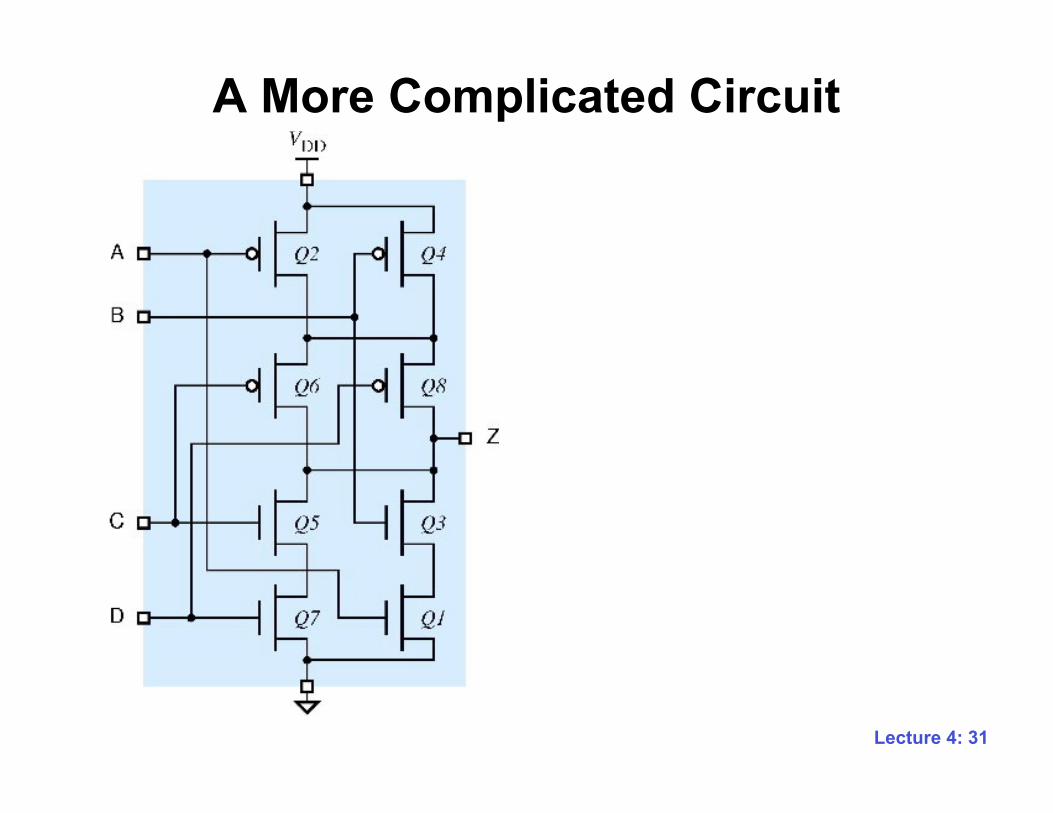
A More Complicated Circuit

Lecture 4: 32
Next Time
Combinational Building Blocks