ece 101 introduction to electrical and computer engineering lab
TRANSCRIPT

ECE 101 Introduction to Electrical and Computer
Engineering
Laboratory and Experiment Guide
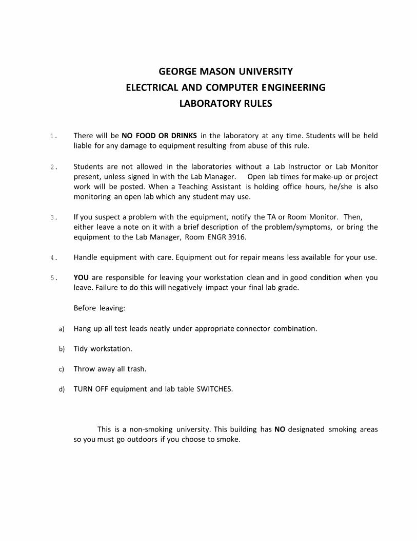
GEORGE MASON UNIVERSITY ELECTRICAL AND COMPUTER ENGINEERING
LABORATORY RULES
1. There will be NO FOOD OR DRINKS in the laboratory at any time. Students will be held liable for any damage to equipment resulting from abuse of this rule.
2. Students are not allowed in the laboratories without a Lab Instructor or Lab Monitor present, unless signed in with the Lab Manager. Open lab times for make-up or project work will be posted. When a Teaching Assistant is holding office hours, he/she is also monitoring an open lab which any student may use.
3. If you suspect a problem with the equipment, notify the TA or Room Monitor. Then, either leave a note on it with a brief description of the problem/symptoms, or bring the equipment to the Lab Manager, Room ENGR 3916.
4. Handle equipment with care. Equipment out for repair means less available for your use.
5. YOU are responsible for leaving your workstation clean and in good condition when you leave. Failure to do this will negatively impact your final lab grade. Before leaving:
a) Hang up all test leads neatly under appropriate connector combination. b) Tidy workstation. c) Throw away all trash. d) TURN OFF equipment and lab table SWITCHES.
This is a non-smoking university. This building has NO designated smoking areas so you must go outdoors if you choose to smoke.

ELECTRONICS SAFETY Exercise of good judgment and knowledge will ensure you a safe laboratory experience. Do not defeat any safety device such as a fuse or circuit breaker, by shorting across it or by using a higher amperage fuse than that specified by the manufacturer. Avoid direct contact with any voltage source. Do not wear rings, watches, bracelets, or dangling necklaces while working on equipment. Do not grasp any exposed metal in your circuit when the power is on. Keep hands dry. Water and perspiration increase conductivity. Wear shoes with insulating soles. Measure voltages with one hand held behind you or in your pocket. Avoid eye injury when cutting off excessive wire lengths. Point the wires downward toward your table top so the cut pieces cannot fly toward your eyes or another person’s. Shut off the power when connecting components or test equipment to a circuit. Double check your wiring before you apply power. Make sure your circuit is properly grounded. Beware of a possible floating ground. It is a good idea to connect all grounds together before applying power. To prevent power terminals from shorting, keep the leads coming from those terminals apart. Your exercise of common sense, safety precautions and knowledge will help you avoid the dangers of electricity. The amount of current required to become lethal depends upon:
1. The person involved and state of health 2. Area of the body involved 3. Length of time the shock is received and 4. Type of electrical current.
Severe electrical shock will cause burns and/or paralysis. A small current passing through the chest can kill. With even minor electrical shock, some people react by going into traumatic shock.
In case of accident, turn off power immediately and call 911. If you suspect someone is touching a "live" wire, do not touch them. Use something non-conductive to push, rather than pull, them away from the wire. An injured person should be kept lying down until medical personnel arrive, and should be kept warm to help prevent traumatic shock.Be sure nothing is done to cause further injury.

GEORGE MASON UNIVERSITY ELECTRICAL AND COMPUTER ENGINNERING LAB TIPS
1) Instruction manuals for the laboratory equipment may be checked out from the lab
manager in room 3916. It is essential that you become familiar with the correct way to use the basic equipment in your first lab course. Wire cutters/strippers are available for sale or you will need to bring your own.
2) Twenty-two gauge wires (22AWG) is the best size to use with the trainers and solder less breadboards. Solid wire only, never stranded, is used for the trainers. There are spools of wire cabled to the back shelf. You will need to cut some and strip the insulation at both ends. Keep jumper wires short. Strive for a neat and logical layout. This will make troubleshooting easier and successful circuits more likely. Strip no more than approximately 3/8 inch of insulation from your jumper wires. Exposed wire increases the risk of short circuits.
3) Using more than one color of wire will help you debug your circuits. Normally RED and BLACK are reserved for power and ground.
4) Probe tips should not be inserted into the solder less breadboard. Wrap a wire around your probe hook tip twice for stability and insert the other end into the connector block. Alligator clips on the equipment leads also need a wrapped wire for connection to the trainers and breadboards.
5) Always ground your probe, but keep the ground wire short. Use the method of wire wrapping described in the previous tip to attach to the alligator clip of the probe ground wire.
6) For any potentiometers (such as most multi-turn) which require adjusting, a trimpot tool is available for purchase from room ENGR 3916. It is included in appropriate kits.
7) Most of the chips used in your lab are not overly static sensitive. However, you should observe some precautions when handling them. If you were issued a tube, it protects the chips from static charges, and is sturdy enough to provide protection to the delicate, metal pin legs.
8) Keep your chips away from magnets, motors and high temperatures. Don't leave them in your car in the sun or extreme cold. They do best in the moderate temperatures most humans prefer.
LAB TIPS CONTINUED
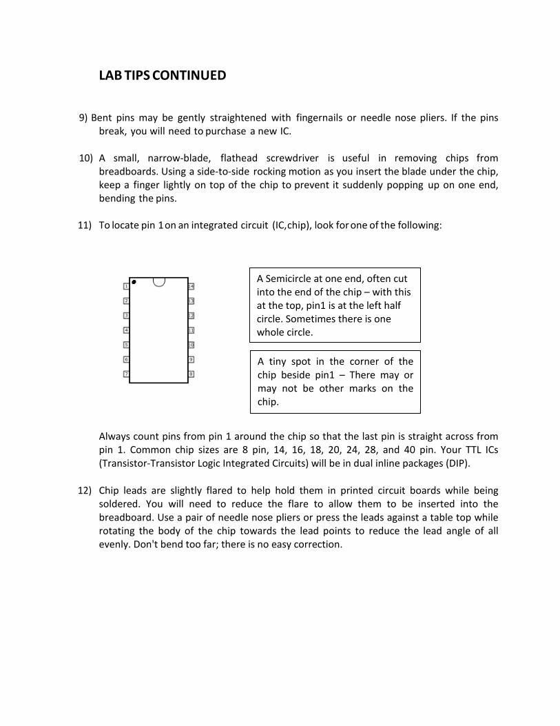
9) Bent pins may be gently straightened with fingernails or needle nose pliers. If the pins break, you will need to purchase a new IC.
10) A small, narrow-blade, flathead screwdriver is useful in removing chips from breadboards. Using a side-to-side rocking motion as you insert the blade under the chip, keep a finger lightly on top of the chip to prevent it suddenly popping up on one end, bending the pins.
11) To locate pin 1 on an integrated circuit (IC, chip), look for one of the following:
Always count pins from pin 1 around the chip so that the last pin is straight across from pin 1. Common chip sizes are 8 pin, 14, 16, 18, 20, 24, 28, and 40 pin. Your TTL ICs (Transistor-Transistor Logic Integrated Circuits) will be in dual inline packages (DIP).
12) Chip leads are slightly flared to help hold them in printed circuit boards while being soldered. You will need to reduce the flare to allow them to be inserted into the breadboard. Use a pair of needle nose pliers or press the leads against a table top while rotating the body of the chip towards the lead points to reduce the lead angle of all evenly. Don't bend too far; there is no easy correction.
A Semicircle at one end, often cut into the end of the chip – with this at the top, pin1 is at the left half circle. Sometimes there is one whole circle.
A tiny spot in the corner of the chip beside pin1 – There may or may not be other marks on the chip.
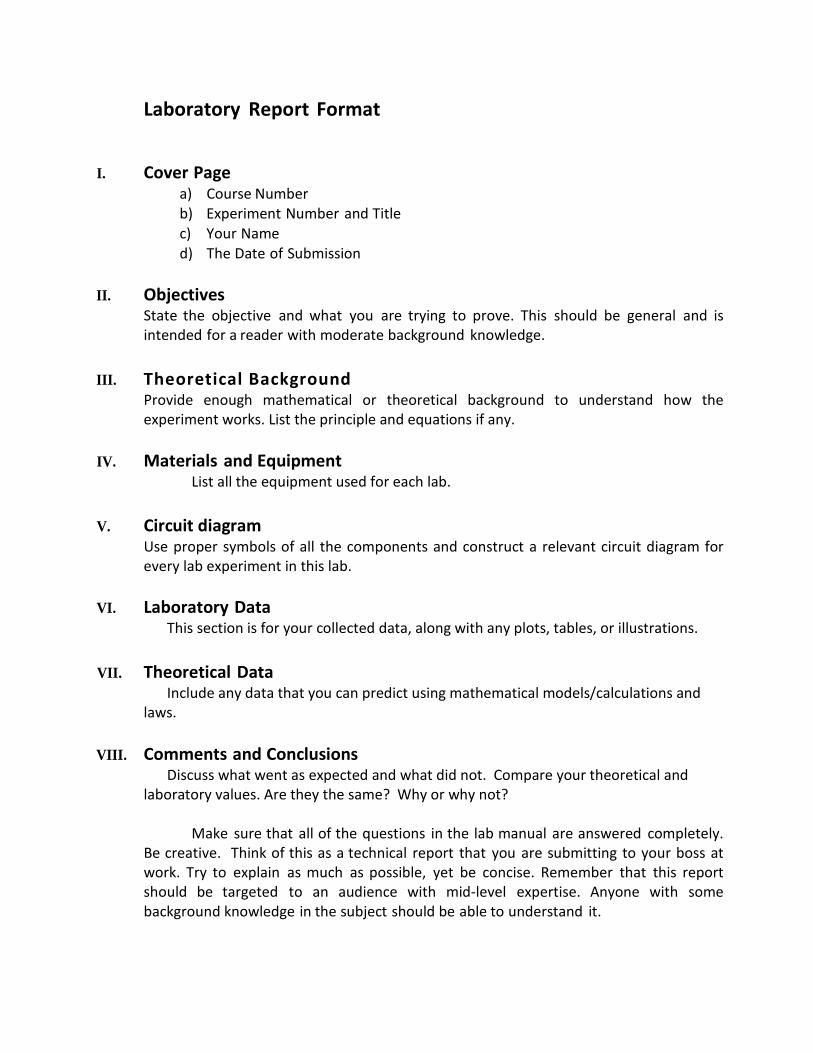
Laboratory Report Format
I. Cover Page a) Course Number b) Experiment Number and Title c) Your Name d) The Date of Submission
II. Objectives
State the objective and what you are trying to prove. This should be general and is intended for a reader with moderate background knowledge.
III. Theoretical Background Provide enough mathematical or theoretical background to understand how the experiment works. List the principle and equations if any.
IV. Materials and Equipment List all the equipment used for each lab.
V. Circuit diagram Use proper symbols of all the components and construct a relevant circuit diagram for every lab experiment in this lab.
VI. Laboratory Data This section is for your collected data, along with any plots, tables, or illustrations.
VII. Theoretical Data Include any data that you can predict using mathematical models/calculations and
laws.
VIII. Comments and Conclusions Discuss what went as expected and what did not. Compare your theoretical and
laboratory values. Are they the same? Why or why not?
Make sure that all of the questions in the lab manual are answered completely. Be creative. Think of this as a technical report that you are submitting to your boss at work. Try to explain as much as possible, yet be concise. Remember that this report should be targeted to an audience with mid-level expertise. Anyone with some background knowledge in the subject should be able to understand it.

ECE 101 Lab Manual
Table of Contents Fall 2015
Laboratory Experiment Student Signature TA Signature
1. Laboratory Fundamentals
2. DC Circuits
3. A Simple Communication System
4. Introduction to the Oscilloscope
5. Simple Filtering
6. Transistor Fundamentals
7. The Transistor as an Amplifier
8. Combinational Logic
9. Smart Buttons (extra credit)
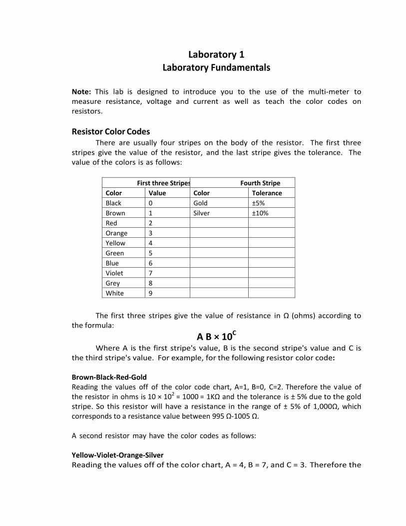
Laboratory 1 Laboratory Fundamentals
Note: This lab is designed to introduce you to the use of the multi-meter to measure resistance, voltage and current as well as teach the color codes on resistors. Resistor Color Codes
There are usually four stripes on the body of the resistor. The first three stripes give the value of the resistor, and the last stripe gives the tolerance. The value of the colors is as follows:
First three Stripes Fourth Stripe Color Value Color Tolerance Black 0 Gold ±5% Brown 1 Silver ±10% Red 2 Orange 3 Yellow 4 Green 5 Blue 6 Violet 7 Grey 8 White 9
The first three stripes give the value of resistance in Ω (ohms) according to
the formula: A B × 10C
Where A is the first stripe's value, B is the second stripe's value and C is the third stripe's value. For example, for the following resistor color code: Brown-Black-Red-Gold Reading the values off of the color code chart, A=1, B=0, C=2. Therefore the value of the resistor in ohms is 10 × 102 = 1000 = 1KΩ and the tolerance is ± 5% due to the gold stripe. So this resistor will have a resistance in the range of ± 5% of 1,000Ω, which corresponds to a resistance value between 995 Ω-1005 Ω. A second resistor may have the color codes as follows: Yellow-Violet-Orange-Silver Reading the values off of the color chart, A = 4, B = 7, and C = 3. Therefore the

value of the resistor in ohms is 47 × 103 = 47,000 = 47KΩ and the tolerance is ± 10%, due to the silver stripe. Part 1) Resistor Measurement
Locate all of the resistors from your kit. Locate the power button of the multi-meter and turn it on. Take two banana to alligator plug wires (one red and one black) and connect the red wire's banana end to the hole marked Ω (usually a red hole) on the multi-meter, and the black wire's banana end to the hole marked "Ground" or "Common" (usually a black hole) on the multi-meter. Connect the alligator ends of these wires to the wires coming from a resistor. When using an auto-ranging multi-meter, the value of the resistance should come up as soon as the wires are connected. For those multi-meters with manual ranging, you will have to adjust the range such that the value with the most significant digits as possible is shown on the LCD display. For this lab, measure each of the resistors in the kit noting down for each resistor the color code on the resistor, the value that the color code indicates, and the measured value of the resistor as seen on the multi-meter. Complete the table below with these values.
Part 2) Voltage Measurement
In an electrical circuit, voltages and currents can be measured and reflect the flow of electrons through electrically conducting materials. A voltage occurs whenever there is a surplus of electrons at one point of the circuit relative to another. A non-zero voltage can occur only between two points in a circuit that are NOT connected via an ideal conductor. One says, a voltage can only drop across a resistor. To equalize this imbalance, electrons flow through the resistor and give rise to electric currents. A voltage is introduced into an electrical circuit via a voltage source such as a battery. Voltages are measured in volts (V) and currents are measured in amperes (A).
Color code based value of the resistor
Measured value of the resistor
Tolerance value
Calculated resistance range of resistor (xΩ-yΩ)
Is the measured resistance value within the designated tolerance limits?
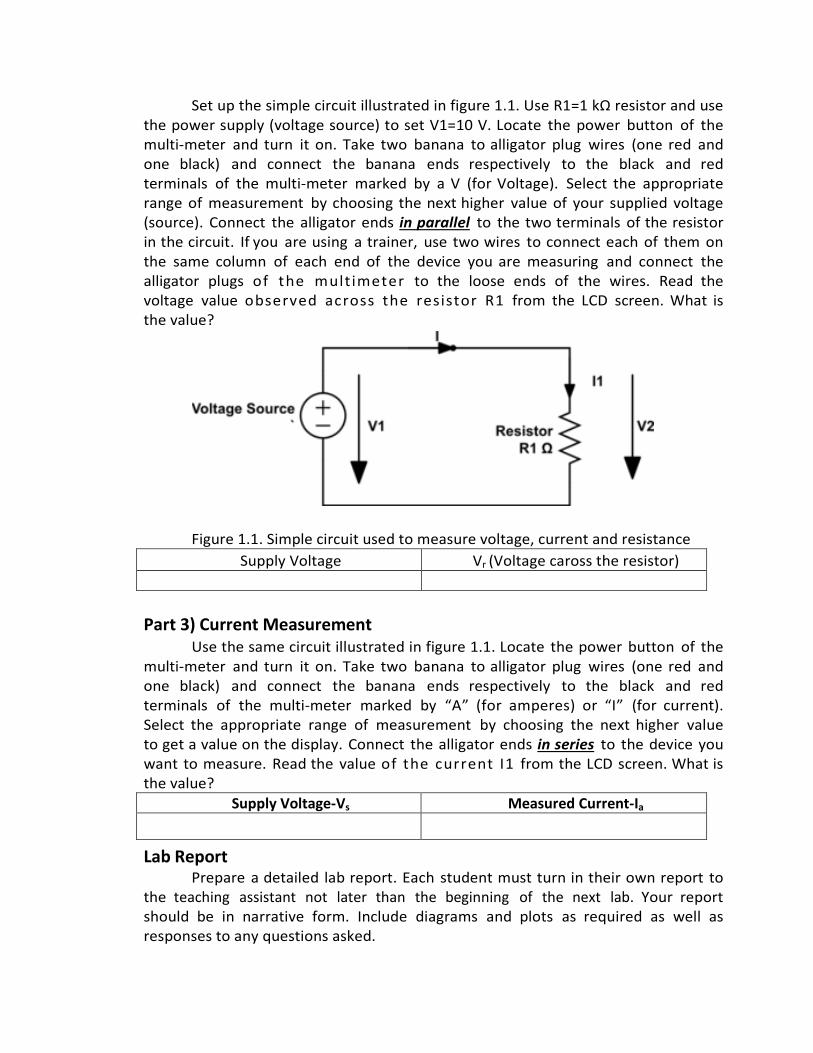
Set up the simple circuit illustrated in figure 1.1. Use R1=1 kΩ resistor and use the power supply (voltage source) to set V1=10 V. Locate the power button of the multi-meter and turn it on. Take two banana to alligator plug wires (one red and one black) and connect the banana ends respectively to the black and red terminals of the multi-meter marked by a V (for Voltage). Select the appropriate range of measurement by choosing the next higher value of your supplied voltage (source). Connect the alligator ends in parallel to the two terminals of the resistor in the circuit. If you are using a trainer, use two wires to connect each of them on the same column of each end of the device you are measuring and connect the alligator plugs of the mult imeter to the loose ends of the wires. Read the voltage value observed across the resistor R1 from the LCD screen. What is the value?
Figure 1.1. Simple circuit used to measure voltage, current and resistance
Supply Voltage Vr (Voltage caross the resistor)
Part 3) Current Measurement
Use the same circuit illustrated in figure 1.1. Locate the power button of the multi-meter and turn it on. Take two banana to alligator plug wires (one red and one black) and connect the banana ends respectively to the black and red terminals of the multi-meter marked by “A” (for amperes) or “I” (for current). Select the appropriate range of measurement by choosing the next higher value to get a value on the display. Connect the alligator ends in series to the device you want to measure. Read the value of the current I1 from the LCD screen. What is the value?
Supply Voltage-Vs Measured Current-Ia
Lab Report
Prepare a detailed lab report. Each student must turn in their own report to the teaching assistant not later than the beginning of the next lab. Your report should be in narrative form. Include diagrams and plots as required as well as responses to any questions asked.

Laboratory 2 DC Circuits
The relationship between voltages and currents in any circuit obeys three
simple rules that we will study in the experiments below. The three rules are: • Ohm's law • Kirchhoff's current law (KCL) • Kirchhoff's voltage law (KVL)
Ohm's law states that the current through a resistor is proportional to the voltage across the resistor and inversely proportional to the resistance of the resistor. This is often expressed via the simple formula: I = V/R or V=IR or R=V/I
Where I denotes the current through the resistor, R denotes the resistor's resistance, and V denotes the voltage across the resistor.
Figure 2.1: Ohm's law predicts the relationship between current and voltage for a resistor.
Kirchhoff's current law ( K C L ) states that any current flowing into a node must also flow out again. Hence, it implies that currents cannot be stored in "regular" circuit elements. The most common application of this law occurs in the case when a circuit branches as shown below.

Figure 2.2: The current I1 equals I2 + I3 Kirchhoff's voltage law (KVL) states that the sum of all voltages in a circuit mesh must equal zero. This is simply a consequence of our earlier observation that a voltage can exist only across resistive elements. To illustrate consider the figure below:
Figure 2.3: Kirchhoff s voltage law implies that V1 equals V2
Preparation Read the background material above and the information that you learned in Laboratory 1. Anticipate the results of the experiments below.
Experiments The following experiments are intended to teach you to use a multimeter for measuring voltages, currents, and resistances.
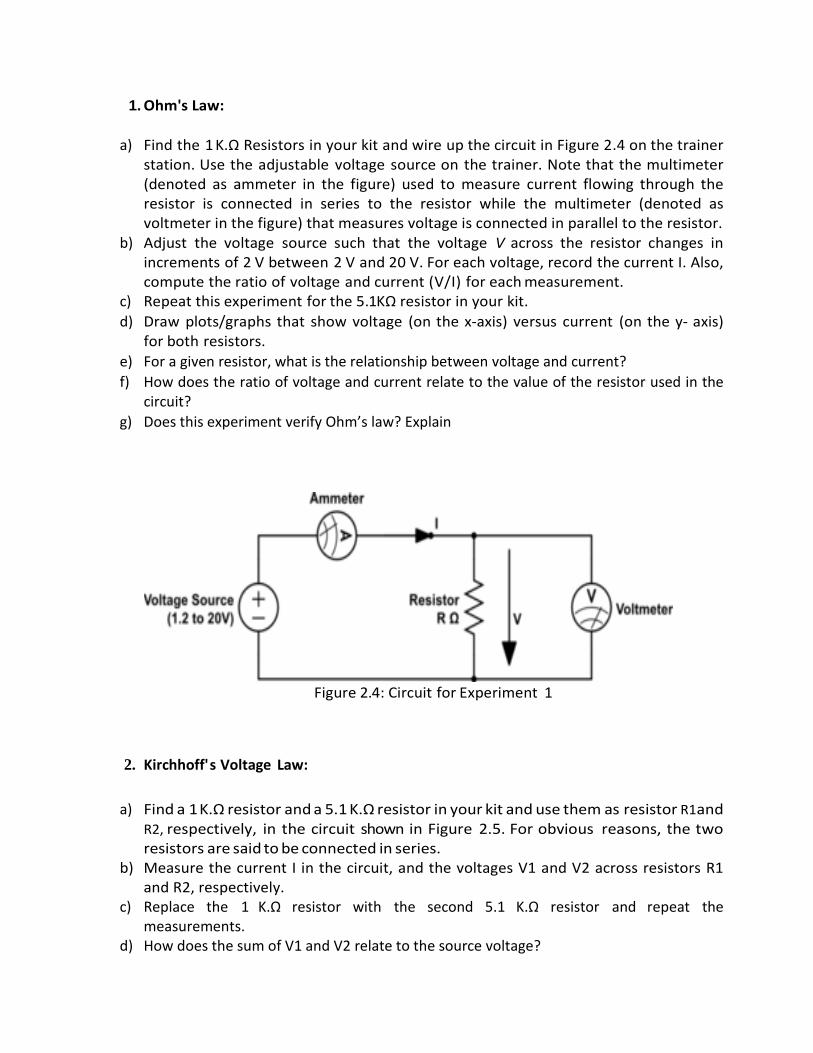
1. Ohm's Law:
a) Find the 1 K.Ω Resistors in your kit and wire up the circuit in Figure 2.4 on the trainer station. Use the adjustable voltage source on the trainer. Note that the multimeter (denoted as ammeter in the figure) used to measure current flowing through the resistor is connected in series to the resistor while the multimeter (denoted as voltmeter in the figure) that measures voltage is connected in parallel to the resistor.
b) Adjust the voltage source such that the voltage V across the resistor changes in increments of 2 V between 2 V and 20 V. For each voltage, record the current I. Also, compute the ratio of voltage and current (V/I) for each measurement.
c) Repeat this experiment for the 5.1KΩ resistor in your kit. d) Draw plots/graphs that show voltage (on the x-axis) versus current (on the y- axis)
for both resistors. e) For a given resistor, what is the relationship between voltage and current? f) How does the ratio of voltage and current relate to the value of the resistor used in the
circuit? g) Does this experiment verify Ohm’s law? Explain
Figure 2.4: Circuit for Experiment 1
2. Kirchhoff' s Voltage Law:
a) Find a 1 K.Ω resistor and a 5.1 K.Ω resistor in your kit and use them as resistor R1 and R2, respectively, in the circuit shown in Figure 2.5. For obvious reasons, the two resistors are said to be connected in series.
b) Measure the current I in the circuit, and the voltages V1 and V2 across resistors R1 and R2, respectively.
c) Replace the 1 K.Ω resistor with the second 5.1 K.Ω resistor and repeat the measurements.
d) How does the sum of V1 and V2 relate to the source voltage?
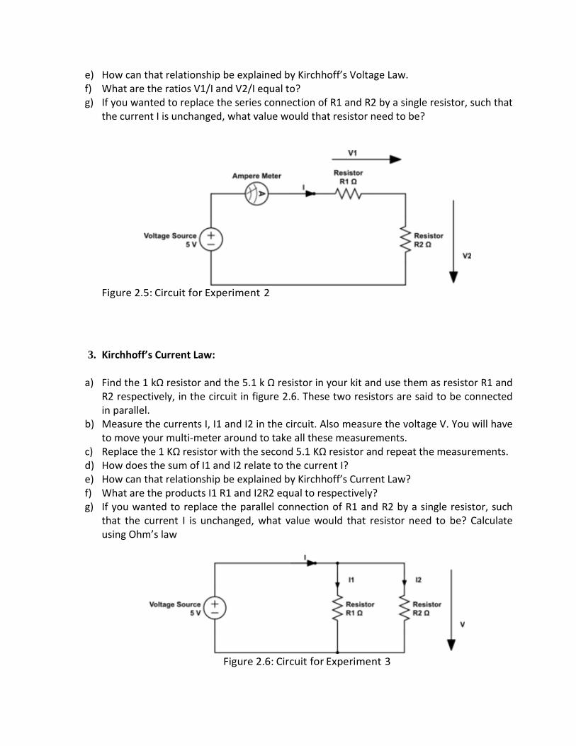
e) How can that relationship be explained by Kirchhoff’s Voltage Law. f) What are the ratios V1/I and V2/I equal to? g) If you wanted to replace the series connection of R1 and R2 by a single resistor, such that
the current I is unchanged, what value would that resistor need to be?
Figure 2.5: Circuit for Experiment 2
3. Kirchhoff’s Current Law:
a) Find the 1 kΩ resistor and the 5.1 k Ω resistor in your kit and use them as resistor R1 and R2 respectively, in the circuit in figure 2.6. These two resistors are said to be connected in parallel.
b) Measure the currents I, I1 and I2 in the circuit. Also measure the voltage V. You will have to move your multi-meter around to take all these measurements.
c) Replace the 1 KΩ resistor with the second 5.1 KΩ resistor and repeat the measurements. d) How does the sum of I1 and I2 relate to the current I? e) How can that relationship be explained by Kirchhoff’s Current Law? f) What are the products I1 R1 and I2R2 equal to respectively? g) If you wanted to replace the parallel connection of R1 and R2 by a single resistor, such
that the current I is unchanged, what value would that resistor need to be? Calculate using Ohm’s law
Figure 2.6: Circuit for Experiment 3
Lab Report
Prepare a detailed lab report. Each student must turn in their own report to the teaching assistant not later than the beginning of the next lab. Your report should be in narrative form. Include diagrams and plots as required as well as responses to any questions asked.

Laboratory 3 A Simple Communication System
Preparation
• Review class notes on "Encoding in Binary Format". • Design an encoding table for mapping the 26 characters in the alphabet plus space (
), comma (,), and period (.) into a binary representation. You could simply use 7 bit or 8 bit ASCII encoding but there are more efficient forms of encoding for this limited set of characters. You will have to bring a sheet to the lab that clearly shows the encoding you designed. It must be clear enough to be interpreted by another person! Experiments
1. Light emitting diode (LED)
• Connect a 1kΩ resistor and the red LED in series to the adjustable voltage source. Make sure that the input voltage supply is initially set at 0V
• Vary the input voltage between 1.2V and 5V and measure the current through the diode and the voltage across the diode. Record also if the diode is lit or not. Vary the voltage in steps of 0.1 V between 1.2 V and 2 V, and in steps of 0.5 V between 2 V and 5 V.
• Turn the LED around and repeat the previous measurements. • Summarize your measurements in two graphs that show voltage across the diode
versus current through the diode for each of the two possible orientations of the diode. Indicate on your graph the range of currents and voltages for which the diode was lit.
2. Telegraph
• Add a switch in series with your resistor and diode (LED). The diode should be oriented such that it lights up when you push the button on your switch. You may have to experiment a little with the switch to determine how to connect it.
• Build a second identical circuit using your second (differently colored) diode. Test your circuits and verify that the diodes light up when you push the corresponding
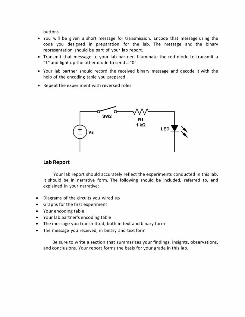
buttons. • You will be given a short message for transmission. Encode that message using the
code you designed in preparation for the lab. The message and the binary representation should be part of your lab report.
• Transmit that message to your lab partner. Illuminate the red diode to transmit a "1" and light up the other diode to send a "0".
• Your lab partner should record the received binary message and decode it with the help of the encoding table you prepared.
• Repeat the experiment with reversed roles.
Lab Report
Your lab report should accurately reflect the experiments conducted in this lab. It should be in narrative form. The following should be included, referred to, and explained in your narrative:
• Diagrams of the circuits you wired up • Graphs for the first experiment • Your encoding table • Your lab partner's encoding table • The message you transmitted, both in text and binary form • The message you received, in binary and text form
Be sure to write a section that summarizes your findings, insights, observations,
and conclusions. Your report forms the basis for your grade in this lab.

Laboratory 4 Introduction to oscilloscope Preparation Read the following document on the Introduction to Oscilloscopes: https://ece.gmu.edu/sites/ece/files/student-resource/7911/oscilloscope-manual.pdf
Be sure that you understand the following terms:
• sine wave • square wave • amplitude • period • frequency • phase • trigger • probe
Experiments:
1. Using the Oscilloscope a) Build a simple circuit in which you connect the function generator (your voltage
source) to a 1 KΩ resistor. b) Set the function generator to produce sine waves of frequency 1 KHz and amplitude
2 Volts (Vp). c) Display the voltage across the resistor on the oscilloscope. Be sure to record all
relevant settings of the control knobs. d) Increase and decrease the amplitude of the signal and describe the effect on the
trace displayed on the oscilloscope. e) Increase and decrease the frequency of the signal and describe the effect on the
trace displayed on the oscilloscope. f) On graph paper, plot a trace you observed. Be sure to include the grid lines on the
oscilloscopes. Accurately label your plot by indicating amplitudes and times corresponding to the grid lines.
g) Explain how you can determine the frequency of the sine wave from the plot you recorded.
h) Repeat the last two assignments for a sinusoid of frequency 100 KHz. i) Repeat steps b-h for a square waveform.
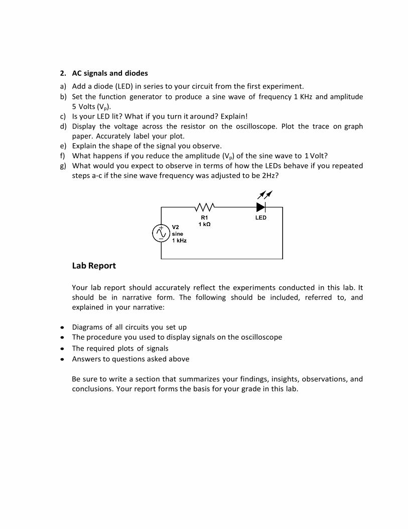
2. AC signals and diodes
a) Add a diode (LED) in series to your circuit from the first experiment. b) Set the function generator to produce a sine wave of frequency 1 KHz and amplitude
5 Volts (Vp). c) Is your LED lit? What if you turn it around? Explain! d) Display the voltage across the resistor on the oscilloscope. Plot the trace on graph
paper. Accurately label your plot. e) Explain the shape of the signal you observe. f) What happens if you reduce the amplitude (Vp) of the sine wave to 1 Volt? g) What would you expect to observe in terms of how the LEDs behave if you repeated
steps a-c if the sine wave frequency was adjusted to be 2Hz?
Lab Report Your lab report should accurately reflect the experiments conducted in this lab. It should be in narrative form. The following should be included, referred to, and explained in your narrative:
• Diagrams of all circuits you set up • The procedure you used to display signals on the oscilloscope • The required plots of signals • Answers to questions asked above
Be sure to write a section that summarizes your findings, insights, observations, and conclusions. Your report forms the basis for your grade in this lab.
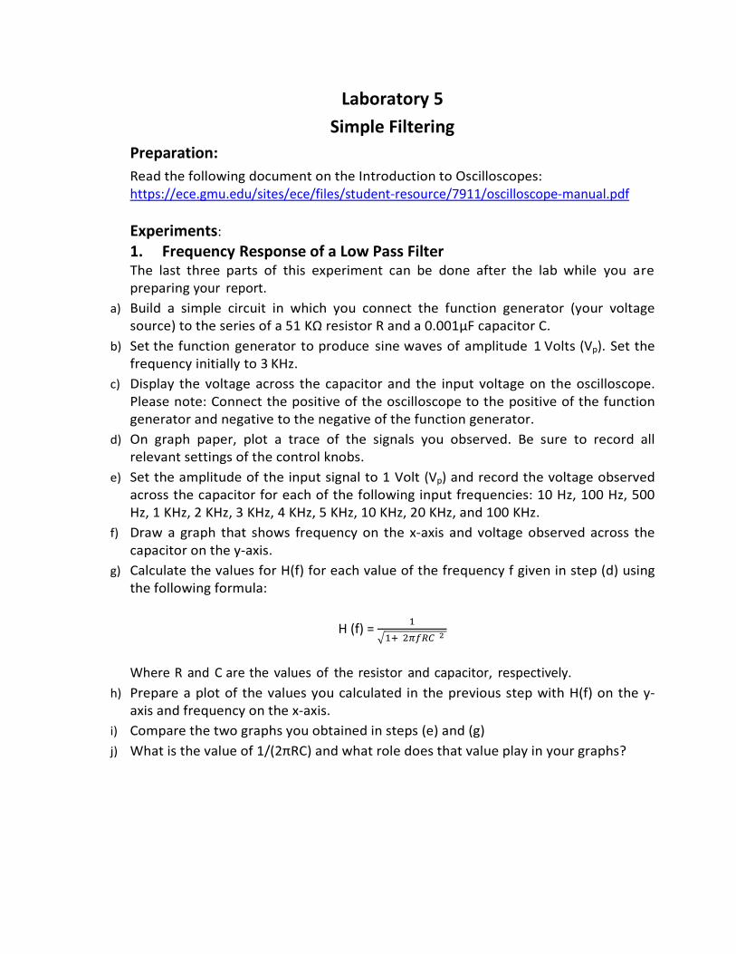
Laboratory 5 Simple Filtering
Preparation: Read the following document on the Introduction to Oscilloscopes: https://ece.gmu.edu/sites/ece/files/student-resource/7911/oscilloscope-manual.pdf Experiments: 1. Frequency Response of a Low Pass Filter The last three parts of this experiment can be done after the lab while you are preparing your report.
a) Build a simple circuit in which you connect the function generator (your voltage source) to the series of a 51 KΩ resistor R and a 0.001µF capacitor C.
b) Set the function generator to produce sine waves of amplitude 1 Volts (Vp). Set the frequency initially to 3 KHz.
c) Display the voltage across the capacitor and the input voltage on the oscilloscope. Please note: Connect the positive of the oscilloscope to the positive of the function generator and negative to the negative of the function generator.
d) On graph paper, plot a trace of the signals you observed. Be sure to record all relevant settings of the control knobs.
e) Set the amplitude of the input signal to 1 Volt (Vp) and record the voltage observed across the capacitor for each of the following input frequencies: 10 Hz, 100 Hz, 500 Hz, 1 KHz, 2 KHz, 3 KHz, 4 KHz, 5 KHz, 10 KHz, 20 KHz, and 100 KHz.
f) Draw a graph that shows frequency on the x-axis and voltage observed across the capacitor on the y-axis.
g) Calculate the values for H(f) for each value of the frequency f given in step (d) using the following formula:
H (f) = 11+(2𝜋𝜋𝜋𝜋)2
Where R and C are the values of the resistor and capacitor, respectively. h) Prepare a plot of the values you calculated in the previous step with H(f) on the y-
axis and frequency on the x-axis. i) Compare the two graphs you obtained in steps (e) and (g) j) What is the value of 1/(2πRC) and what role does that value play in your graphs?

Fig 4-1: Low pass filter-sine wave input
2. Passing a Square Wave through a Low Pass Filter a) Use the same circuit as in the previous experiment. Set the function generator to
produce square waves of amplitude 1 Volt (Vp). b) Record the waveform of the voltage across the capacitor when the input frequency is
100 Hz. c) Record the waveform of the voltage across the capacitor when the input frequency
is 3 KHz. d) What can you say about the difference in the waveforms that you observed in steps
b) and c)? e) What could be one practical application of this observation?
Fig 4-2: Low pass filter square wave input
3. Rectifier a) Set up the circuit in the diagram below. b) Set the function generator to produce a sine wave of frequency 3 KHz and amplitude
3 Volts (Vp). c) Display the voltage across the capacitor C1 and the voltage across the resistor R1.
Plot these voltages on a graph paper. d) Repeat s t e p s a - c for a frequency of 30 KHz. e) Explain the shape of the signals you observe in each case (there will be 4 graphs in
total) f) Suggest a practical use for a circuit like this. Think of a voltage source with a
frequency of 60 Hz.
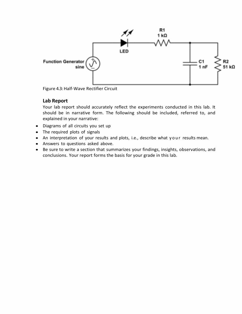
Figure 4.3: Half-Wave Rectifier Circuit Lab Report Your lab report should accurately reflect the experiments conducted in this lab. It should be in narrative form. The following should be included, referred to, and explained in your narrative:
• Diagrams of all circuits you set up • The required plots of signals • An interpretation of your results and plots, i.e., describe what y o u r results mean. • Answers to questions asked above. • Be sure to write a section that summarizes your findings, insights, observations, and
conclusions. Your report forms the basis for your grade in this lab.
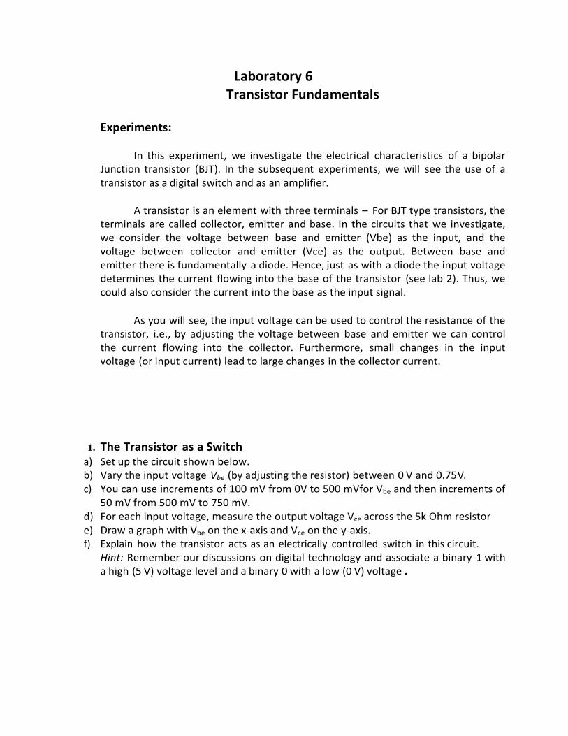
Laboratory 6 Transistor Fundamentals
Experiments:
In this experiment, we investigate the electrical characteristics of a bipolar
Junction transistor (BJT). In the subsequent experiments, we will see the use of a transistor as a digital switch and as an amplifier.
A transistor is an element with three terminals – For BJT type transistors, the terminals are called collector, emitter and base. In the circuits that we investigate, we consider the voltage between base and emitter (Vbe) as the input, and the voltage between collector and emitter (Vce) as the output. Between base and emitter there is fundamentally a diode. Hence, just as with a diode the input voltage determines the current flowing into the base of the transistor (see lab 2). Thus, we could also consider the current into the base as the input signal.
As you will see, the input voltage can be used to control the resistance of the transistor, i.e., by adjusting the voltage between base and emitter we can control the current flowing into the collector. Furthermore, small changes in the input voltage (or input current) lead to large changes in the collector current.
1. The Transistor as a Switch a) Set up the circuit shown below. b) Vary the input voltage Vbe (by adjusting the resistor) between 0 V and 0.75 V. c) You can use increments of 100 mV from 0V to 500 mVfor Vbe and then increments of
50 mV from 500 mV to 750 mV. d) For each input voltage, measure the output voltage Vce across the 5k Ohm resistor e) Draw a graph with Vbe on the x-axis and Vce on the y-axis. f) Explain how the transistor acts as an electrically controlled switch in this circuit.
Hint: Remember our discussions on digital technology and associate a binary 1 with a high (5 V) voltage level and a binary 0 with a low (0 V) voltage .

Figure 5 . 2 : Circuit diagram showing transistor used as a switch. Vbe(mV) Vce(mV) 0 100 200 300 400 500 550 600 650 700 750
2. Electrical Characteristics of a Transistor
a) Set up the circuit in the diagram below. You will have to use the constant 5 Volt supply and the adjustable 1kΩ resistor to set the voltage Vbe· You will also have to use the adjustable (1.2V-20V) voltage supply to set the voltage Vce. These values will have to be set in the next steps.
b) Adjust the 1kΩ resistor such that the voltage between base and emitter (Vbe) takes on values between 550 mV and 750 mV in increments of 50 mV.
c) For each of these voltages Vbe, vary the voltage Vce between collector and emitter from 1 V to 10 V in increments of 1 V. For each combination of Vbe and Vce measure and record the current lc flowing into the collector.
d) Plot the results of your measurements in one graph which shows the collector current Ic (y-axis) versus the voltage Vce (x-axis) for each of the different voltages Vbe·
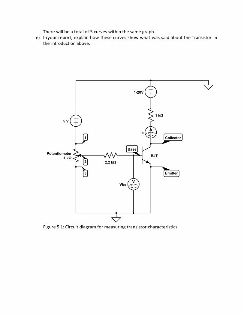
There will be a total of 5 curves within the same graph. e) In your report, explain how these curves show what was said about the Transistor in
the introduction above.
Figure 5.1: Circuit diagram for measuring transistor characteristics.

Lab Data:
Vce (V) Ic (mA)
Vbe=550mV Vbe=600mV Vbe=650mV Vbe=700mV Vbe=750mV 1 2 3
4 5 6 7
8 9 10 Lab Report Your lab report should accurately reflect the experiments conducted in this lab. It should be in narrative form. The following should be included, referred to, and explained in your narrative:
• Diagrams of all circuits you set up, • The required plots, • An interpretation of your results and plots, i.e., describe what your results mean, • Answers to questions asked above.
Be sure to write a section that summarizes your findings, insights, observations, and conclusions. Your report forms the basis for your grade in this lab.

Laboratory 7 Transistor as an Amplifier
Experiment: In this experiment, we exploit the electrical characteristics of a bipolar junction transistor (BJT) to construct a simple amplifier. The Transistor as an Amplifier
a) Set up the circuit in the diagram below. Use the constant 12 Volt supply and the adjustable 1 kΩ resistor to set the voltage Vbe to approximately 0.6 V.
b) Use the function generator for the input voltage. Use a sinusoidal input of frequency 10 KHz and set the amplitude to the smallest possible value. I.e., turn the amplitude knob all the way to the left.
c) On the oscilloscope, use two probes to display the input voltage and the output voltage on the same screen. Record the waveforms you observe.
d) Measure the amplitude of the input voltage (Vp-p) and the output voltage (Vp-p). e) Vary the input voltage carefully and observe the effect on the output voltage. f) In particular, observe the ratio of the amplitudes of output and input voltage. g) At what input voltage does the shape of the output waveform begin to change?
Record the waveform you are observing. h) Replace the 2kΩ resistor with a 5kΩ resistor and repeat the experiments above. i) In your report, answer the following questions j) Please graph your input and output waveforms.
• In what way do the values of the resistors that are connected to the collector and the emitter, respectively affect the ratio of output voltage and input voltage?

Figure 6.1: Circuit diagram for a simple amplifier.
Lab Report Your lab report should accurately reflect the experiments conducted in this lab. It should be in narrative form. The following should be included, referred to, and explain in your narrative:
• Diagrams of all circuits you set up, • The required plots, • An interpretation of your results and plots, i.e., describe what your results mean, • Answers to questions asked above.
Be sure to write a section that summarizes your findings, insights, observations, and conclusions. Your report forms the basis for your grade in this lab.

Laboratory 8 Combinational Logic
Preparation: Read lecture notes on combinational logic. Experiments
1. Digital Logic Chips a) Take each of the two chips, 74LS08 and 74LS86, that you received and connect them as follows:
• Connect the pin immediately to the right of the notch in the casing to +5 V • Connect the pin diagonally across from the first one to ground, • Connect the top two pins to the left of the notch to two different DIP switches on the
trainer • Connect the third pin from the top to the left of the notch to an LED.
b) For each of the four possible combinations of the two DIP switches, record if the LED is lit. c) Summarize your findings in a truth table. You will need to create a truth table for each chip d) Which logic function does each of these chips achieve?
2. Half Adder a) Set up the logic circuit in the diagram below. Do not forget to connect the supply voltage p i n
VCC to the power supply (5V) and the ground pin to ground! b) Use DIP switches for the inputs A and B, and LEDs for the outputs Sum and Carry. c) Determine the truth table for this circuit. d) Describe the function of this circuit, i.e., explain why it is called a half adder.
Figure 7.1: Half Adder

3. 2-Bit Full Adder a) Set up the logic circuit in the diagram below. Each box labeled "Half Adder" contains the circuit
from the previous diagram. b) Use DIP switches for the inputs A1, A2, B1, and B2, and LEDs for the outputs S1 S 2, and Carry. c) Create the truth table for this circuit. d) Describe the function of this circuit, i.e., explain why it is called a 2-bit adder.
Figure 7 .2: 2-Bit Full Adder
Lab Report Your lab report should accurately reflect the experiments conducted in this lab. It should be in narrative form. The following should be included, referred to, and explained in your narrative:
• Diagrams of all circuits you set up • The required plots • An interpretation of your results and plots, i.e., describe what your results mean • Answers to questions asked above.
Be sure to write a section that summarizes your findings, insights, observations, and conclusions. Your report forms the basis for your grade in this lab.
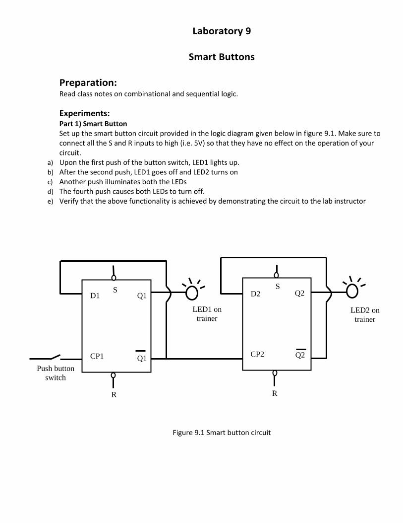
Laboratory 9
Smart Buttons
Preparation: Read class notes on combinational and sequential logic. Experiments: Part 1) Smart Button Set up the smart button circuit provided in the logic diagram given below in figure 9.1. Make sure to connect all the S and R inputs to high (i.e. 5V) so that they have no effect on the operation of your circuit.
a) Upon the first push of the button switch, LED1 lights up. b) After the second push, LED1 goes off and LED2 turns on c) Another push illuminates both the LEDs d) The fourth push causes both LEDs to turn off. e) Verify that the above functionality is achieved by demonstrating the circuit to the lab instructor
Figure 9.1 Smart button circuit
Q1
R R
D1
CP1
Q1 S S
Push button switch
LED2 on trainer
LED1 on trainer
D2
CP2
Q2
Q2
S
Part 2) Jeopardy Button a) Set up the Jeopardy Button circuit as shown in figure 9.2 below. (make sure to connect the set inputs
to high i.e. 5V) b) Experiment and verify its operation. c) Explain how two players can use this circuit to play jeopardy d) How can this circuit be reset to be used again by the two players?
Lab Report Your lab report should accurately reflect the experiments conducted in this lab. It should be in narrative form. The following should be included, referred to, and explained in your narrative:
• Diagrams of all circuits you set up • The procedure you used to display signals on the oscilloscope • The required plots of signals • Answers to questions
Be sure to write a section that summarizes your findings, insights, observations, and conclusions. Your report forms the basis for your grade in this lab.
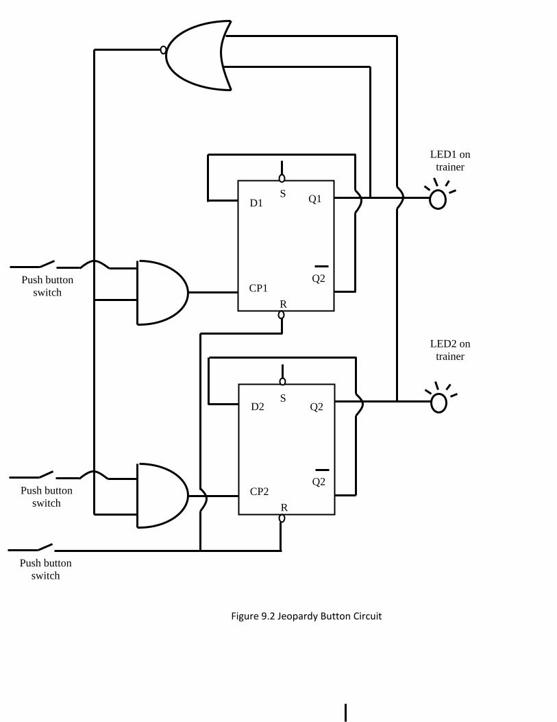
Figure 9.2 Jeopardy Button Circuit
LED1 on trainer
LED2 on trainer
Q1
D1
CP1 ( )
Q1
R
Q2
Q1
D2
CP2 ( )
Q2
R
Q2
Push button switch
Push button switch
S
S
Push button switch
APPENDIX A Data Pages
74LS02 74LS08 74LS74
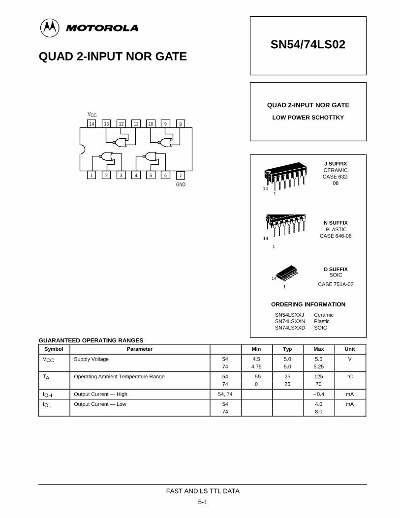
QUAD 2-INPUT NOR GATE
SN54/74LS02
VCC 14 13 12 11 10 9 8
QUAD 2-INPUT NOR GATE
LOW POWER SCHOTTKY
1 2 3 4 5 6
7
GND
J SUFFIX CERAMIC CASE 632-
08 14
1
N SUFFIX PLASTIC
14 CASE 646-06
1
D SUFFIX SOIC
14
1 CASE 751A-02
ORDERING INFORMATION
SN54LSXXJ Ceramic SN74LSXXN Plastic SN74LSXXD SOIC
GUARANTEED OPERATING RANGES Symbol Parameter Min Typ Max Unit
VCC Supply Voltage 54 4.5 5.0 5.5 V 74 4.75 5.0 5.25
TA Operating Ambient Temperature Range 54 –55 25 125 °C 74 0 25 70
IOH Output Current — High 54, 74 – 0.4 mA IOL Output Current — Low 54 4.0 mA
74 8.0
FAST AND LS TTL DATA
5-1
SN54/74LS02
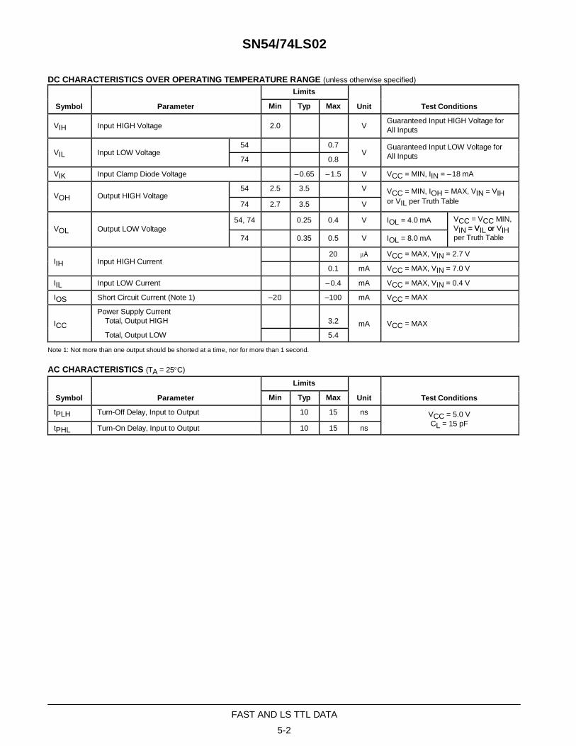
DC CHARACTERISTICS OVER OPERATING TEMPERATURE RANGE (unless otherwise specified)
Symbol
Parameter Limits
Unit
Test Conditions Min Typ Max
VIH
Input HIGH Voltage
2.0 V Guaranteed Input HIGH Voltage for
All Inputs
VIL
Input LOW Voltage 54 0.7
V Guaranteed Input LOW Voltage for All Inputs 74 0.8
VIK Input Clamp Diode Voltage – 0.65 – 1.5 V VCC = MIN, IIN = – 18 mA
VOH
Output HIGH Voltage 54 2.5 3.5 V VCC = MIN, IOH = MAX, VIN = VIH
or VIL per Truth Table 74 2.7 3.5 V
VOL
Output LOW Voltage 54, 74 0.25 0.4 V IOL = 4.0 mA VCC = VCC MIN,
VIN == VVIL oorr VIH per Truth Table 74 0.35 0.5 V IOL = 8.0 mA
IIH
Input HIGH Current 20 µA VCC = MAX, VIN = 2.7 V
0.1 mA VCC = MAX, VIN = 7.0 V IIL Input LOW Current – 0.4 mA VCC = MAX, VIN = 0.4 V IOS Short Circuit Current (Note 1) –20 –100 mA VCC = MAX
ICC
Power Supply Current Total, Output HIGH
Total, Output LOW
3.2
mA
VCC = MAX 5.4
Note 1: Not more than one output should be shorted at a time, nor for more than 1 second.
AC CHARACTERISTICS (TA = 25°C)
Symbol
Parameter Limits
Unit
Test Conditions Min Typ Max tPLH Turn-Off Delay, Input to Output 10 15 ns VCC = 5.0 V
CL = 15 pF tPHL Turn-On Delay, Input to Output 10 15 ns
FAST AND LS TTL DATA
5-2

QUAD 2-INPUT AND GATE
SN54/74LS08
VCC 14 13 12 11 10 9 8
QUAD 2-INPUT AND GATE
LOW POWER SCHOTTKY
1 2 3 4 5 6
7
GND
J SUFFIX CERAMIC CASE 632-
08 14
1
N SUFFIX PLASTIC
14 CASE 646-06
1
D SUFFIX SOIC
14
1 CASE 751A-02
ORDERING INFORMATION
SN54LSXXJ Ceramic SN74LSXXN Plastic SN74LSXXD SOIC
GUARANTEED OPERATING RANGES Symbol Parameter Min Typ Max Unit
VCC Supply Voltage 54 4.5 5.0 5.5 V 74 4.75 5.0 5.25
TA Operating Ambient Temperature Range 54 –55 25 125 °C 74 0 25 70
IOH Output Current — High 54, 74 – 0.4 mA IOL Output Current — Low 54 4.0 mA
74 8.0
FAST AND LS TTL DATA
5-1

SN54/74LS08
DC CHARACTERISTICS OVER OPERATING TEMPERATURE RANGE (unless otherwise specified)
Symbol
Parameter Limits
Unit
Test Conditions Min Typ Max
VIH
Input HIGH Voltage
2.0 V Guaranteed Input HIGH Voltage for
All Inputs
VIL
Input LOW Voltage 54 0.7
V Guaranteed Input LOW Voltage for All Inputs 74 0.8
VIK Input Clamp Diode Voltage – 0.65 – 1.5 V VCC = MIN, IIN = – 18 mA
VOH
Output HIGH Voltage 54 2.5 3.5 V VCC = MIN, IOH = MAX, VIN = VIH
or VIL per Truth Table 74 2.7 3.5 V
VOL
Output LOW Voltage 54, 74 0.25 0.4 V IOL = 4.0 mA VCC = VCC MIN,
VIN == VVIL oorr VIH per Truth Table 74 0.35 0.5 V IOL = 8.0 mA
IIH
Input HIGH Current 20 µA VCC = MAX, VIN = 2.7 V
0.1 mA VCC = MAX, VIN = 7.0 V IIL Input LOW Current – 0.4 mA VCC = MAX, VIN = 0.4 V IOS Short Circuit Current (Note 1) –20 – 100 mA VCC = MAX
ICC
Power Supply Current Total, Output HIGH
Total, Output LOW
4.8
mA
VCC = MAX 8.8
Note 1: Not more than one output should be shorted at a time, nor for more than 1 second.
AC CHARACTERISTICS (TA = 25°C)
Symbol
Parameter Limits
Unit
Test Conditions Min Typ Max tPLH Turn-Off Delay, Input to Output 8.0 15 ns VCC = 5.0 V
CL = 15 pF tPHL Turn-On Delay, Input to Output 10 20 ns
FAST AND LS TTL DATA
5-2
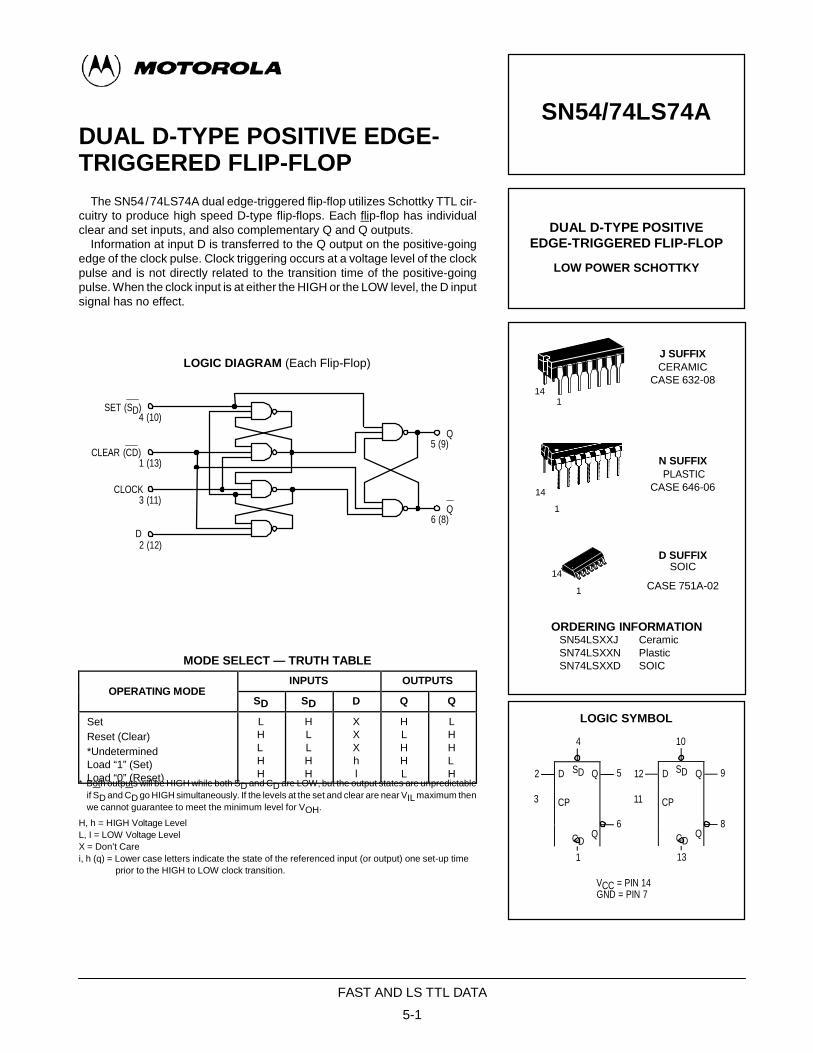
DUAL D-TYPE POSITIVE EDGE-TRIGGERED FLIP-FLOP
The SN54 / 74LS74A dual edge-triggered flip-flop utilizes Schottky TTL cir- cuitry to produce high speed D-type flip-flops. Each flip-flop has individual clear and set inputs, and also complementary Q and Q outputs.
Information at input D is transferred to the Q output on the positive-going edge of the clock pulse. Clock triggering occurs at a voltage level of the clock pulse and is not directly related to the transition time of the positive-going pulse. When the clock input is at either the HIGH or the LOW level, the D input signal has no effect.
SN54/74LS74A
DUAL D-TYPE POSITIVE EDGE-TRIGGERED FLIP-FLOP
LOW POWER SCHOTTKY
SET (SD) 4 (10)
CLEAR (CD) 1 (13)
CLOCK
3 (11)
D 2 (12)
LOGIC DIAGRAM (Each Flip-Flop)
Q 5 (9)
Q 6 (8)
J SUFFIX CERAMIC
CASE 632-08 14
1
N SUFFIX PLASTIC
14 CASE 646-06
1
D SUFFIX SOIC
14
1 CASE 751A-02
MODE SELECT — TRUTH TABLE
ORDERING INFORMATION SN54LSXXJ Ceramic SN74LSXXN Plastic SN74LSXXD SOIC
LOGIC SYMBOL
4 10
* Both outputs will be HIGH while both SD and CD are LOW, but the output states are unpredictable if SD and CD go HIGH simultaneously. If the levels at the set and clear are near VIL maximum then we cannot guarantee to meet the minimum level for VOH.
H, h = HIGH Voltage Level L, I = LOW Voltage Level X = Don’t Care i, h (q) = Lower case letters indicate the state of the referenced input (or output) one set-up time
prior to the HIGH to LOW clock transition.
2 D Q
3
1
5 12
11
6
D Q 9
8
13
VCC = PIN 14 GND = PIN 7
FAST AND LS TTL DATA
5-1
OPERATING MODE
INPUTS OUTPUTS SD SD D Q Q
Set Reset (Clear) *Undetermined Load “1” (Set) Load “0” (Reset)
L H L H H
H L L H H
X X X h l
H L H H L
L H H L H
SD
CP
CD Q
SD
CP
CD Q
SN54/74LS74A
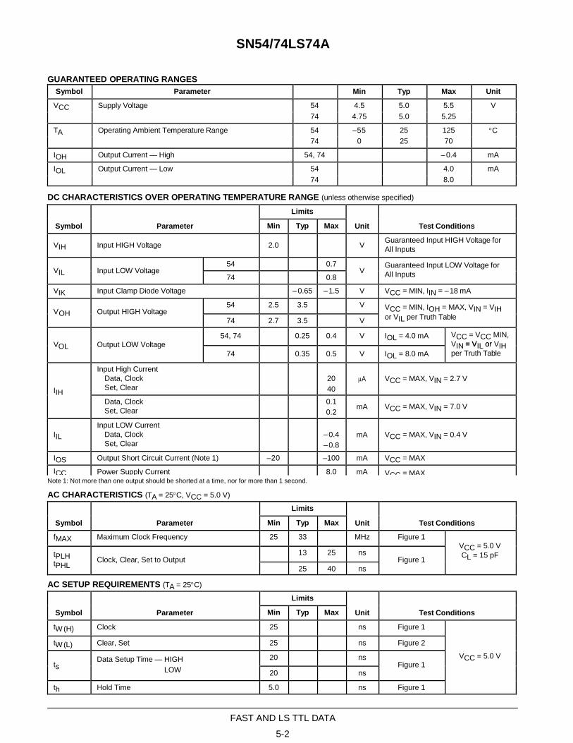
GUARANTEED OPERATING RANGES Symbol Parameter Min Typ Max Unit
VCC Supply Voltage 54 4.5 5.0 5.5 V 74 4.75 5.0 5.25
TA Operating Ambient Temperature Range 54 –55 25 125 °C 74 0 25 70
IOH Output Current — High 54, 74 – 0.4 mA IOL Output Current — Low 54 4.0 mA
74 8.0 DC CHARACTERISTICS OVER OPERATING TEMPERATURE RANGE (unless otherwise specified)
OH
Note 1: Not more than one output should be shorted at a time, nor for more than 1 second.
AC CHARACTERISTICS (TA = 25°C, VCC = 5.0 V)
Symbol
Parameter Limits
Unit
Test Conditions Min Typ Max fMAX Maximum Clock Frequency 25 33 MHz Figure 1
VCC = 5.0 V CL = 15 pF tPLH
tPHL
Clock, Clear, Set to Output 13 25 ns Figure 1
25 40 ns AC SETUP REQUIREMENTS (TA = 25°C)
Symbol
Parameter Limits
Unit
Test Conditions Min Typ Max tW (H) Clock 25 ns Figure 1
VCC = 5.0 V tW (L) Clear, Set 25 ns Figure 2
ts Data Setup Time — HIGH
LOW 20 ns
Figure 1 20 ns
th Hold Time 5.0 ns Figure 1
FAST AND LS TTL DATA
5-2
Symbol
Parameter Limits
Unit
Test Conditions Min Typ Max
VIH Input HIGH Voltage 2.0 V Guaranteed Input HIGH Voltage for All Inputs
VIL
Input LOW Voltage 54 0.7
V Guaranteed Input LOW Voltage for All Inputs 74 0.8
VIK Input Clamp Diode Voltage – 0.65 – 1.5 V VCC = MIN, IIN = – 18 mA
V
Output HIGH Voltage 54 2.5 3.5 V VCC = MIN, IOH = MAX, VIN = VIH or VIL per Truth Table 74 2.7 3.5 V
VOL
Output LOW Voltage 54, 74 0.25 0.4 V IOL = 4.0 mA VCC = VCC MIN,
VIN == VVIL oorr VIH per Truth Table 74 0.35 0.5 V IOL = 8.0 mA
IIH
Input High Current Data, Clock Set, Clear
20 40
µA
VCC = MAX, VIN = 2.7 V
Data, Clock Set, Clear 0.1
0.2 mA VCC = MAX, VIN = 7.0 V
IIL
Input LOW Current Data, Clock Set, Clear
– 0.4 – 0.8
mA
VCC = MAX, VIN = 0.4 V
IOS Output Short Circuit Current (Note 1) –20 –100 mA VCC = MAX ICC Power Supply Current 8.0 mA VCC = MAX

SN54/74LS74A
AC WAVEFORMS
D* 1.3 V 1.3 V
th(L)
th(H)
ts(L) tW(H)
1.3 V CP
tPHL Q
1.3 V
1 fMAX
tW(L)
ts(H)
tPLH
1.3 V
1.3 V
tPLH tPHL
1.3 V Q
1.3 V
*The shaded areas indicate when the input is permitted to change for predictable output performance.
Figure 1. Clock to Output Delays, Data
Set-Up and Hold Times, Clock Pulse Width
SET
tW
1.3 V 1.3 V
tW
CLEAR
1.3 V 1.3 V
tPLH tPHL
1.3 V Q
tPHL
1.3 V
tPLH
Q 1.3 V
1.3 V
Figure 2. Set and Clear to Output Delays, Set and Clear Pulse Widths
FAST AND LS TTL DATA
5-3
QUAD 2-INPUT EXCLUSIVE OR GATE
SN54/74LS86
QUAD 2-INPUT EXCLUSIVE OR GATE
VCC 14 13 12 11 10 9 8
LOW POWER SCHOTTKY
1 2 3 4 5 6
TRUTH TABLE
7
GND
J SUFFIX CERAMIC CASE 632-
08 14
1
N SUFFIX PLASTIC
14 CASE 646-06
1
D SUFFIX SOIC
14
1 CASE 751A-02
ORDERING INFORMATION
SN54LSXXJ Ceramic SN74LSXXN Plastic SN74LSXXD SOIC
GUARANTEED OPERATING RANGES Symbol Parameter Min Typ Max Unit
VCC Supply Voltage 54 4.5 5.0 5.5 V 74 4.75 5.0 5.25
TA Operating Ambient Temperature Range 54 –55 25 125 °C 74 0 25 70
IOH Output Current — High 54, 74 – 0.4 mA IOL Output Current — Low 54 4.0 mA
74 8.0
FAST AND LS TTL DATA
5-1
IN OUT A B Z L L L L H H H L H H H L
SN54/74LS
86
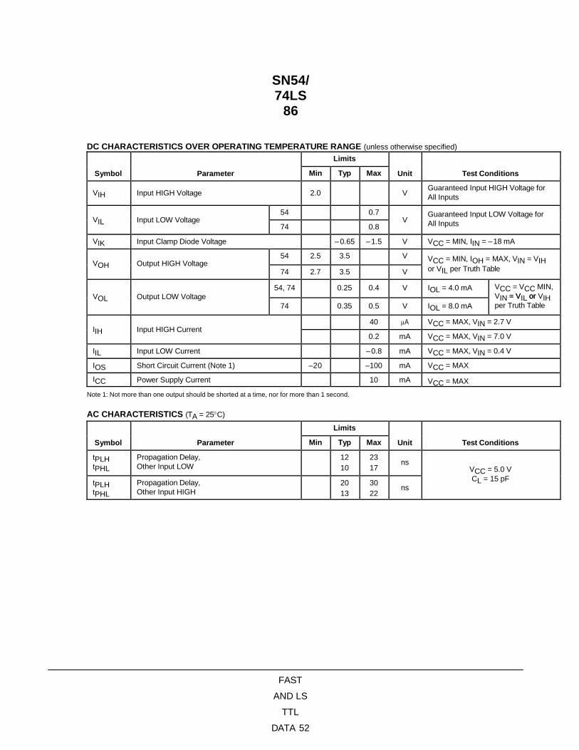
DC CHARACTERISTICS OVER OPERATING TEMPERATURE RANGE (unless otherwise specified)
Symbol
Parameter Limits
Unit
Test Conditions Min Typ Max
VIH
Input HIGH Voltage
2.0 V Guaranteed Input HIGH Voltage for
All Inputs
VIL
Input LOW Voltage 54 0.7
V Guaranteed Input LOW Voltage for All Inputs 74 0.8
VIK Input Clamp Diode Voltage – 0.65 – 1.5 V VCC = MIN, IIN = – 18 mA
VOH
Output HIGH Voltage 54 2.5 3.5 V VCC = MIN, IOH = MAX, VIN = VIH
or VIL per Truth Table 74 2.7 3.5 V
VOL
Output LOW Voltage 54, 74 0.25 0.4 V IOL = 4.0 mA VCC = VCC MIN,
VIN == VVIL oorr VIH per Truth Table 74 0.35 0.5 V IOL = 8.0 mA
IIH
Input HIGH Current 40 µA VCC = MAX, VIN = 2.7 V
0.2 mA VCC = MAX, VIN = 7.0 V IIL Input LOW Current – 0.8 mA VCC = MAX, VIN = 0.4 V IOS Short Circuit Current (Note 1) –20 –100 mA VCC = MAX ICC Power Supply Current 10 mA VCC = MAX
Note 1: Not more than one output should be shorted at a time, nor for more than 1 second.
AC CHARACTERISTICS (TA = 25°C)
Symbol
Parameter Limits
Unit
Test Conditions Min Typ Max tPLH tPHL
Propagation Delay, Other Input LOW
12 10
23 17
ns
VCC = 5.0 V CL = 15 pF tPLH
tPHL Propagation Delay, Other Input HIGH
20 13
30 22
ns
FAST
AND LS
TTL
DATA 52