ec7451: microprocessor and microcontroller iii- peripherals and... · ec7451: microprocessor and...
TRANSCRIPT

EC7451: MICROPROCESSOR AND MICROCONTROLLER
Dr. V. SATHIESH KUMAR Department of Electronics Engg., MIT 1
Presentation Slides:
www.sathieshkumar.com/tutorials
Unit III : PERIPHERALS AND INTERFACING 1. Programmable Peripheral Interface (8255) 2. Keyboard display controller (8279) 3. ADC0808 and DAC0808 Interface 4. Programmable Timer Controller (8254) 5. Programmable interrupt controller (8259) 6. Serial Communication Interface (8251)
TEXT BOOK K. Udaya Kumar, B. S. Umashankar, “The 8085 Microprocessors: Architecture, Programming and Interfacing". Pearson Education. 2008.
Presented By,
Dr. V. Sathiesh Kumar Department of Electronics Engg.,
MIT-Anna University
EC7451: MICROPROCESSOR AND MICROCONTROLLER UNIT III –Peripherals & Interfacing
Dr. V. SATHIESH KUMAR Department of Electronics Engg., MIT 2
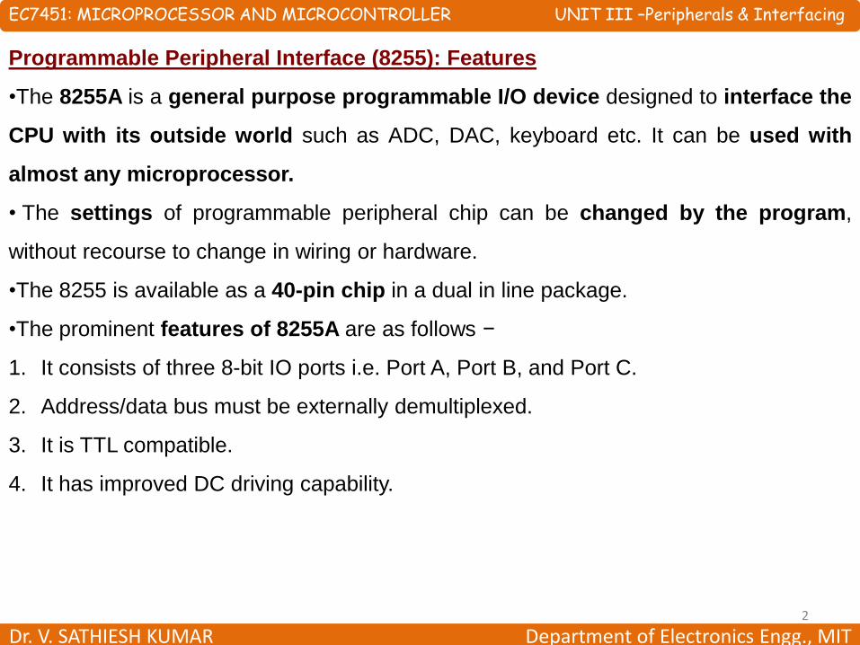
Programmable Peripheral Interface (8255): Features
•The 8255A is a general purpose programmable I/O device designed to interface the
CPU with its outside world such as ADC, DAC, keyboard etc. It can be used with
almost any microprocessor.
• The settings of programmable peripheral chip can be changed by the program,
without recourse to change in wiring or hardware.
•The 8255 is available as a 40-pin chip in a dual in line package.
•The prominent features of 8255A are as follows −
1. It consists of three 8-bit IO ports i.e. Port A, Port B, and Port C.
2. Address/data bus must be externally demultiplexed.
3. It is TTL compatible.
4. It has improved DC driving capability.

EC7451: MICROPROCESSOR AND MICROCONTROLLER UNIT III –Peripherals & Interfacing
Dr. V. SATHIESH KUMAR Department of Electronics Engg., MIT 3
Programmable Peripheral Interface (8255): Features
•D0-D7 data bus lines are available to read/write data into the ports or control register
using RD and WR.
• Address lines A1 and A0 allow to successively access any one of the ports or the
control register.
• CS is used to enable 8255 chip
• On Reset, all the ports are initialized as input line
A1 A0 PORT SELECTED
0 0 PORTA
0 1 PORTB
1 0 PORTC
1 1 Control Register
EC7451: MICROPROCESSOR AND MICROCONTROLLER UNIT III –Peripherals & Interfacing
Dr. V. SATHIESH KUMAR Department of Electronics Engg., MIT 4
Programmable Peripheral Interface (8255):
•It consists of three 8-bit bidirectional I/O ports (24 I/O lines, PORT A, PORT B and
PORT C) which can be configured as per the requirement.
•We can assign different ports as input or output functions.
•Port A contains one 8-bit output latch/buffer and one 8-bit input buffer.
•Port B contains one 8-bit output latch/buffer and one 8-bit input buffer.
•Port C can be split into two parts, i.e. PORT C lower (PC0-PC3) and PORT C upper
(PC7-PC4) by the control word. They can be independently programmed as input or
output lines.
•These port pins have the ability to source 1 mA of current at 1.5V, when
programmed to work as output pins.

EC7451: MICROPROCESSOR AND MICROCONTROLLER UNIT III –Peripherals & Interfacing
Dr. V. SATHIESH KUMAR Department of Electronics Engg., MIT 5
Programmable Peripheral Interface (8255):
•These three ports are further divided into two groups:
1. Group A includes PORT A and upper PORT C.
2. Group B includes PORT B and lower PORT C.
•These two groups can be programmed in three different modes:
1.The first mode is named as Mode 0
2.The second mode is named as Mode 1
3.The third mode is named as Mode 2.

EC7451: MICROPROCESSOR AND MICROCONTROLLER UNIT III –Peripherals & Interfacing
Dr. V. SATHIESH KUMAR Department of Electronics Engg., MIT 6
Programmable Peripheral Interface (8255):
•It can work in either BSR (bit set/reset) mode or in I/O mode.

EC7451: MICROPROCESSOR AND MICROCONTROLLER UNIT III –Peripherals & Interfacing
Dr. V. SATHIESH KUMAR Department of Electronics Engg., MIT 7
Programmable Peripheral Interface (8255): Bit Set/Reset Mode (BSR Mode)
•Applicable only to Port C.
• Any line of Port C, which is programmed as output can be set to logic 1, or reset to
logic 0 using the single bit/reset feature of Port C.

EC7451: MICROPROCESSOR AND MICROCONTROLLER UNIT III –Peripherals & Interfacing
Dr. V. SATHIESH KUMAR Department of Electronics Engg., MIT 8
Programmable Peripheral Interface (8255): Input/Output Mode (I/O Mode)
• The functionality of three ports is decided by the contents of the control port.
•The control part can only be written by the microprocessor.
•Intel 8085 cannot read it. Thus, there are three ports which can be used for I/O
operations, and a control port to control the function of these ports.

EC7451: MICROPROCESSOR AND MICROCONTROLLER UNIT III –Peripherals & Interfacing
Dr. V. SATHIESH KUMAR Department of Electronics Engg., MIT 9
Programmable Peripheral Interface (8255): Operating Modes
•8255A has three different operating modes:
1.Mode 0 − It is called as a simple I/O or basic I/O.
•In this mode, Port A and B is used as two 8-bit ports and Port C as two 4-bit ports.
•Each port can be programmed in either input mode or output mode where outputs
are latched and inputs are not latched.
•Thus, the input device must continue with the data on port pins till the port data is
read by the microprocessor. So it is useful for reading switch settings, but not useful
for reading from a keyboard.
•Since the ports in output mode are latched, the microprocessor is not required to
continously send the data to the port till the output device receives the port data.
•It is useful, as an example, for sending data to LED display that updates the display
based on the latched output. Ports do not have interrupt capability.

EC7451: MICROPROCESSOR AND MICROCONTROLLER UNIT III –Peripherals & Interfacing
Dr. V. SATHIESH KUMAR Department of Electronics Engg., MIT 10
Programmable Peripheral Interface (8255): Operating Modes
2. Mode 1 − It is called as strobed I/O or handshake I/O.
•It is useful when, an input device supplies data to the microprocessor at irregular
intervals.
•In this mode, Port A and B is used as 8-bit I/O ports. They can be configured as
either input or output ports.
•If Port A and Port B work in mode 1. Each port uses three lines from Port C as
handshake signals. Remaining two lines of Port C can be used for simple I/O in
mode 0.
•If only Port A or Port B is working in mode 1, then five lines of Port C are free for
use in mode 0.
•Inputs and outputs are latched.

EC7451: MICROPROCESSOR AND MICROCONTROLLER UNIT III –Peripherals & Interfacing
Dr. V. SATHIESH KUMAR Department of Electronics Engg., MIT 11
Programmable Peripheral Interface (8255): Operating Modes
3. Mode 2 − It is a bidirectional handshake I/O.
• Usually in mode 0 or mode 1, a port is required to work as an input port or as an output
port. It depends on whether an input device or an output device is connected to the port.
•In contrast with this mode 2, sometimes microprocessor can receive information,
and at some other times desires to send information to the I/O device.
•In this mode, Port A can be configured as the bidirectional port and Port B either in
Mode 0 or Mode 1.
•Port A uses five signals from Port C as handshake signals for data transfer. The
remaining three signals from Port C can be used either as simple I/O or as
handshake for port B.
EC7451: MICROPROCESSOR AND MICROCONTROLLER UNIT III –Peripherals & Interfacing
Dr. V. SATHIESH KUMAR Department of Electronics Engg., MIT 12
Programmable Peripheral Interface (8255): Operating Modes
•On a summary,
1. Port A can work in mode 0, mode 1 or mode 2.
2. Port B can work in mode 0 or mode 1.
3. Port C works in mode 0 if Port A and Port B are in mode 0. Otherwise, any free lines
of Port C, after allocating handshake lines, are used in mode 0.
• When the 8255 is reset, the Port A, Port B and Port C are initialized to work as
input ports in mode 0.

EC7451: MICROPROCESSOR AND MICROCONTROLLER UNIT III –Peripherals & Interfacing
Dr. V. SATHIESH KUMAR Department of Electronics Engg., MIT 13
Programmable Peripheral Interface (8255): Pin Description

EC7451: MICROPROCESSOR AND MICROCONTROLLER UNIT III –Peripherals & Interfacing
Dr. V. SATHIESH KUMAR Department of Electronics Engg., MIT 14
Programmable Peripheral Interface (8255): Architecture

EC7451: MICROPROCESSOR AND MICROCONTROLLER UNIT III –Peripherals & Interfacing
Dr. V. SATHIESH KUMAR Department of Electronics Engg., MIT 15
Programmable Peripheral Interface (8255): Functional Description
Data Bus Buffer: It is a tristate 8-bit buffer, which is used to interface the
microprocessor to the system data bus. Data is transmitted or received by the buffer
as per the instructions by the CPU. Control words and status information is also
transferred using this bus.
Read/Write Control Logic: This block is responsible for controlling the
internal/external transfer of data/control/status word. It accepts the input from the
CPU address and control buses, and in turn issues command to both the control groups.
Write (WR): This control signal enables the write operation. When this signal goes
low, the microprocessor writes into a selected I/O port or control register.
RESET: This is an active high signal. It clears the control register and sets all ports
in the input mode.

EC7451: MICROPROCESSOR AND MICROCONTROLLER UNIT III –Peripherals & Interfacing
Dr. V. SATHIESH KUMAR Department of Electronics Engg., MIT 16
Programmable Peripheral Interface (8255): Functional Description
Chip Select (CS): A LOW on this input selects the chip and enables the
communication between the 8255A and the CPU. It is connected to the decoded
address, and A0 & A1 are connected to the microprocessor address lines.
Read (RD): This control signal enables the Read operation. When the signal is low,
the microprocessor reads the data from the selected I/O port of the 8255.
CS A1 A0 PORT SELECTED
0 0 0 PORTA
0 0 1 PORTB
0 1 0 PORTC
0 1 1 Control Register
1 X X No Selection

EC7451: MICROPROCESSOR AND MICROCONTROLLER UNIT III –Peripherals & Interfacing
Dr. V. SATHIESH KUMAR Department of Electronics Engg., MIT 17
Programmable Peripheral Interface (8255): Functional Description
A0 and A1: These input signals work with RD, WR, and one of the control signal.
• Following is the table showing their various signals with their result.
A1 A0 RD WR CS Result
0 0 0 1 0 Input Operation
PORT A → Data Bus
0 1 0 1 0 PORT B → Data Bus
1 0 0 1 0 PORT C → Data Bus
0 0 1 0 0 Output Operation
Data Bus → PORT A
0 1 1 0 0 Data Bus → PORT A
1 0 1 0 0 Data Bus → PORT B
1 1 1 0 0 Data Bus → PORT D

EC7451: MICROPROCESSOR AND MICROCONTROLLER UNIT III –Peripherals & Interfacing
Dr. V. SATHIESH KUMAR Department of Electronics Engg., MIT 18
Programmable Peripheral Interface (8255):
• The 8255 can be connected in a microcomputer system as either memory-mapped
I/O or I/O-mapped I/O.
•Suppose we want 8255 connected as I/O-mapped I/O with addresses of Port A, Port
B, Port C, and control port as 20H, 21H, 22H and 23H, respectively.
•Then one of the possible chip select circuit is shown below,

EC7451: MICROPROCESSOR AND MICROCONTROLLER UNIT III –Peripherals & Interfacing
Dr. V. SATHIESH KUMAR Department of Electronics Engg., MIT 19
Programmable Peripheral Interface (8255):
• Suppose we want 8255 connected as memory-mapped I/O with addresses of Port
A, Port B, Port C, and control part as FFFCH, FFFDH, FFFEH, and FFFFH,
respectively.
• Then one of the possible chip select circuit is shown below,

EC7451: MICROPROCESSOR AND MICROCONTROLLER UNIT III –Peripherals & Interfacing
Dr. V. SATHIESH KUMAR Department of Electronics Engg., MIT 20
PPI (8255): Interrupt driven data transfer
• Among the three pins provided by Port C to a port for the purpose of handshake
data transfer, one of them called INT is used for interrupting the microprocessor.
•Actually, Port C provides INTA as interrupt from Port A and INTB as interrupt from
Port B.
•These interrupt request outputs of 8255 can be inhibited by resetting to 0 the
associated EI flip-flop or enabled by setting to 1 the associated EI flip-flop.
•This is accomplished by Port C bit set/reset control function.
•This function allows the user to allow or disallow a specific peripheral to interrupt the
8085, without altering the general interrupt structure.

EC7451: MICROPROCESSOR AND MICROCONTROLLER UNIT III –Peripherals & Interfacing
Dr. V. SATHIESH KUMAR Department of Electronics Engg., MIT 21
PPI (8255): Interrupt driven Input Operation
• Assume, we have an input device that supplies data at irregular intervals.
•Let us say, it is connected to Port B of 8255, which is configured to work in mode 1.

EC7451: MICROPROCESSOR AND MICROCONTROLLER UNIT III –Peripherals & Interfacing
Dr. V. SATHIESH KUMAR Department of Electronics Engg., MIT 22
PPI (8255): Interrupt driven Input Operation
• It makes use of three handshake signals supplied by Port C.
•STB* is an input pin to 8255, and IBF and INT are output pins of 8255.
1. STB* - It is an active low STRobe input pulse to the 8255.
• The peripheral sends a low-going pulse with a minimum width of 500 ns on this
input of 8255 whenever it has data to send to the port.
•When STB makes logic 0 to logic 1 transition the peripheral data on port pins are
latched by the port buffer.
•The data on the port pins should be held for at least 180 ns after this transition.
• For Port A, the signal is called STBA*, and for Port B it is called STBB*.
•This handshake pin is the same as PC4 for Port A and PC2 for Port B.

EC7451: MICROPROCESSOR AND MICROCONTROLLER UNIT III –Peripherals & Interfacing
Dr. V. SATHIESH KUMAR Department of Electronics Engg., MIT 23
PPI (8255): Interrupt driven Input Operation
2. IBF : It is an active high output pin of 8255.
• It indicates input buffer full status to the peripheral and the microprocessor.
•The buffer is called an input buffer, as it is a strobed input operation.
•IBF goes to logic 1 within 300 ns after STB* goes to logic 0.
•IBF goes to logic 0 within 300 ns after the port data is read by the microprocessor.
• For Port A, the signal is called IBFA, and for Port B it is called IBFB.
•The handshake pin is the same as PC5 for Port A and PC1 for Port B.
3. INT: It is an active high output pin of 8255.
•The signal is used to interrupt the microprocessor if interrupt-driven data transfer is
desired.
•If status check data transfer is contemplated, this pin is left open without connecting to
an interrupt pin of the microprocessor.
•For Port A, the interrupt signal is called INTA, and for Port B it is called INTB.
•This handshake pin is the same as PC3 for Port A and PC0 for Port B.

EC7451: MICROPROCESSOR AND MICROCONTROLLER UNIT III –Peripherals & Interfacing
Dr. V. SATHIESH KUMAR Department of Electronics Engg., MIT 24
PPI (8255): Interrupt driven Input Operation

EC7451: MICROPROCESSOR AND MICROCONTROLLER UNIT III –Peripherals & Interfacing
Dr. V. SATHIESH KUMAR Department of Electronics Engg., MIT 25
PPI (8255): Interrupt driven Output Operation
• An output device that needs data at irregular intervals.
•Let us say, output device is connected to Port B of 8255, which is configured to
work in mode 1.

EC7451: MICROPROCESSOR AND MICROCONTROLLER UNIT III –Peripherals & Interfacing
Dr. V. SATHIESH KUMAR Department of Electronics Engg., MIT 26
PPI (8255): Interrupt driven Output Operation
• It makes use of three handshake signals supplied by Port C.
•ACK* is an input pin to 8255, and OBF* and INT are output pins of 8255.
1. ACK* - It is an active low ACKnowledge input pulse to the 8255.
• The peripheral sends a low-going pulse with a minimum width of 300 ns on this
input of 8255 whenever it wants to receive data from the port.
•When ACK* makes logic 1 to 0 transition the latched data in the port is sent out
on the port pins to the output device.
•For Port A, the signal is called ACKA*, and for Port B it is called ACKB*.
•This handshake pin is same as PC6 for Port A and PC2 for Port B.

EC7451: MICROPROCESSOR AND MICROCONTROLLER UNIT III –Peripherals & Interfacing
Dr. V. SATHIESH KUMAR Department of Electronics Engg., MIT 27
PPI (8255): Interrupt driven Output Operation
• It makes use of three handshake signals supplied by Port C.
•ACK* is an input pin to 8255, and OBF* and INT are output pins of 8255.
1. ACK* - It is an active low ACKnowledge input pulse to the 8255.
• The peripheral sends a low-going pulse with a minimum width of 300 ns on this
input of 8255 whenever it wants to receive data from the port.
•When ACK* makes logic 1 to 0 transition the latched data in the port is sent out
on the port pins to the output device.
•For Port A, the signal is called ACKA*, and for Port B it is called ACKB*.
•This handshake pin is same as PC6 for Port A and PC2 for Port B.

EC7451: MICROPROCESSOR AND MICROCONTROLLER UNIT III –Peripherals & Interfacing
Dr. V. SATHIESH KUMAR Department of Electronics Engg., MIT 28
PPI (8255): Interrupt driven Output Operation
2. OBF* - It is an active low output pin of 8255.
• It indicates the output buffer full status to the peripheral and the microprocessor.
•The buffer is called as an output buffer as it is a strobed output operation.
•OBF* goes to logic 0 within 650 ns after WR* goes to logic 1, indicating that the
output buffer has become full.
•OBF* goes to logic 1 within 350 ns after ACK* makes 1 to 0 transition, to indicate
that the port is received by the output device and the buffer has become empty.
•For Port A, the signal is called OBFA*, and for Port B it is called OBFB*.
•This hand shake pin is the same as PC7 for Port A and PC1 for Port B.
EC7451: MICROPROCESSOR AND MICROCONTROLLER UNIT III –Peripherals & Interfacing
Dr. V. SATHIESH KUMAR Department of Electronics Engg., MIT 29
PPI (8255): Interrupt driven Output Operation
3. INT - It is an active high output pin of 8255.
• This signal is used to interrupt the microprocessor if interrupt-driven data transfer is
desired.
•For Port A, the signal is called INTA, and for Port B it is called INTB.
•This hand shake pin is the same as PC3 for Port A and PC0 for Port B.

EC7451: MICROPROCESSOR AND MICROCONTROLLER UNIT III –Peripherals & Interfacing
Dr. V. SATHIESH KUMAR Department of Electronics Engg., MIT 30
PPI (8255): Interrupt driven Output Operation
EC7451: MICROPROCESSOR AND MICROCONTROLLER UNIT III –Peripherals & Interfacing
Dr. V. SATHIESH KUMAR Department of Electronics Engg., MIT 31
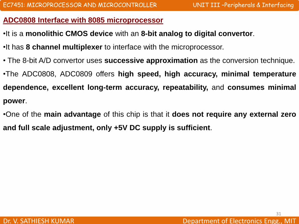
ADC0808 Interface with 8085 microprocessor
•It is a monolithic CMOS device with an 8-bit analog to digital convertor.
•It has 8 channel multiplexer to interface with the microprocessor.
• The 8-bit A/D convertor uses successive approximation as the conversion technique.
•The ADC0808, ADC0809 offers high speed, high accuracy, minimal temperature
dependence, excellent long-term accuracy, repeatability, and consumes minimal
power.
•One of the main advantage of this chip is that it does not require any external zero
and full scale adjustment, only +5V DC supply is sufficient.

EC7451: MICROPROCESSOR AND MICROCONTROLLER UNIT III –Peripherals & Interfacing
Dr. V. SATHIESH KUMAR Department of Electronics Engg., MIT 32
ADC0808 Interface with 8085 microprocessor: Architecture
EC7451: MICROPROCESSOR AND MICROCONTROLLER UNIT III –Peripherals & Interfacing
Dr. V. SATHIESH KUMAR Department of Electronics Engg., MIT 33
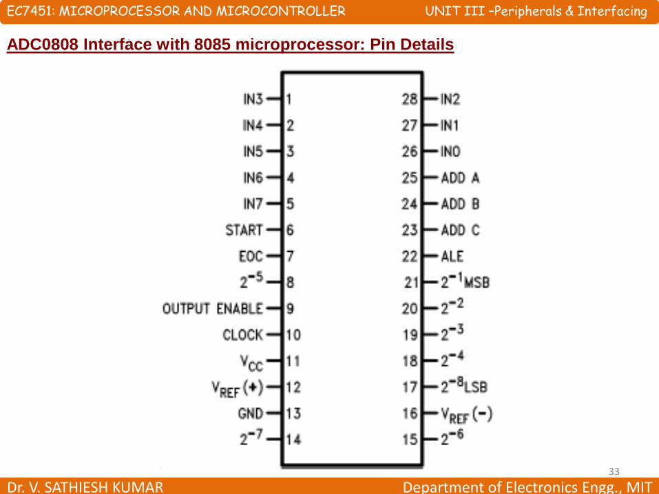
ADC0808 Interface with 8085 microprocessor: Pin Details

EC7451: MICROPROCESSOR AND MICROCONTROLLER UNIT III –Peripherals & Interfacing
Dr. V. SATHIESH KUMAR Department of Electronics Engg., MIT 34
ADC0808:
• The device contains an 8-channel single-ended analog signal multiplexer.
•A particular input channel is selected by using the address decoder.
•The address is latched into the decoder on the low-to-high transition of the address
latch enable (ALE) signal.

EC7451: MICROPROCESSOR AND MICROCONTROLLER UNIT III –Peripherals & Interfacing
Dr. V. SATHIESH KUMAR Department of Electronics Engg., MIT 35
ADC0808 Interface with 8085 microprocessor: Typical Application

EC7451: MICROPROCESSOR AND MICROCONTROLLER UNIT III –Peripherals & Interfacing
Dr. V. SATHIESH KUMAR Department of Electronics Engg., MIT 36
ADC0808 Interface with 8085 microprocessor
•We need 8255 Programmable Peripheral Interface chip with ADC0808.
EC7451: MICROPROCESSOR AND MICROCONTROLLER UNIT III –Peripherals & Interfacing
Dr. V. SATHIESH KUMAR Department of Electronics Engg., MIT 37
ADC0808 Interface with 8085 microprocessor
•The Port A of 8255 chip is used as the input port.
•The PC7 pin of Port Cupper is connected to the End of Conversion (EOC) pin of the
analog to digital converter. This port is also used as input port.
•The Clower port is used as an output port.
•The PC2-0 lines are connected to three address pins (A, B, C) of this chip to select
input channels.
•The PC3 pin is connected to the Start of Conversion (SOC) pin and ALE pin of ADC
0808/0809.

EC7451: MICROPROCESSOR AND MICROCONTROLLER UNIT III –Peripherals & Interfacing
Dr. V. SATHIESH KUMAR Department of Electronics Engg., MIT 38
ADC0808 Interface with 8085 microprocessor
•A program to generate digital signal from analog data. We are using IN0 as input pin,
so the pin selection value will be 00H.
MVI A, 98H ; Set Port A and Cupper as input, CLower as output
OUT 03H ; Write to control Word register
XRA A ; Clear the accumulator
OUT 02H ; Send the content of Acc to Port Clower to select IN0
MVI A, 08H ; Load the accumulator with 08H
OUT 02H ; ALE and SOC will be 1 [High to Low Pulse]
XRA A ; Clear the accumulator
OUT 02H ; ALE and SOC will be low.
READ: IN 02H ; Read from EOC (PC7)
RAL ; Rotate left to check C7 is 1.
JNC READ ; If C7 is not 1, go to READ
IN 00H ; Read digital output of ADC
STA 8000H ; Save result at 8000H
HLT ; Stop the program
ADDRESS
PORT A 00H
PORT B 01H
PORT C 02H
CWR 03H

EC7451: MICROPROCESSOR AND MICROCONTROLLER UNIT III –Peripherals & Interfacing
Dr. V. SATHIESH KUMAR Department of Electronics Engg., MIT 39
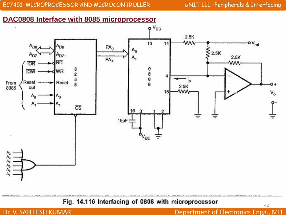
DAC0808 Interface with 8085 microprocessor
DAC 0808 is a 8-bit Digital to Analog Convertor.
Binary weighted DAC and R/2R ladder type
DAC0808 (8-bit) provides 256 discrete voltage or current levels of output
7 6 5 3 04 2 1( )2 4 8 16 32 64 128 256
out ref
D D D D DD D DI I
2refI mA

EC7451: MICROPROCESSOR AND MICROCONTROLLER UNIT III –Peripherals & Interfacing
Dr. V. SATHIESH KUMAR Department of Electronics Engg., MIT 40
DAC0808 Interface with 8085 microprocessor

EC7451: MICROPROCESSOR AND MICROCONTROLLER UNIT III –Peripherals & Interfacing
Dr. V. SATHIESH KUMAR Department of Electronics Engg., MIT 41
DAC0808 Interface with 8085 microprocessor
EC7451: MICROPROCESSOR AND MICROCONTROLLER UNIT III –Peripherals & Interfacing
Dr. V. SATHIESH KUMAR Department of Electronics Engg., MIT 42
DAC0808 Interface with 8085 microprocessor

EC7451: MICROPROCESSOR AND MICROCONTROLLER UNIT III –Peripherals & Interfacing
Dr. V. SATHIESH KUMAR Department of Electronics Engg., MIT 43
DAC0808 Interface with 8085 microprocessor: Square waveform generation
MVI A,80H //I/O mode
OUT 23H
START: MVI A,00H // Low logic level
OUT 20H
CALL DELAY
MVI A,FFH // High logic level
OUT 20H
CALL DELAY
JMP START
DELAY: MVI B,05H //Delay Subroutine
LOOP1: MVI C,FFH
LOOP2: DCR C
JNZ LOOP2
DCR B
JNZ LOOP1
RET
ADDRESS
PORT A 20H
PORT B 21H
PORT C 22H
CWR 23H

EC7451: MICROPROCESSOR AND MICROCONTROLLER UNIT III –Peripherals & Interfacing
Dr. V. SATHIESH KUMAR Department of Electronics Engg., MIT 44
DAC0808 Interface with 8085 microprocessor: Sawtooth waveform generation
MVI A,80H //I/O mode
OUT 23H
START: MVI A,00H // Low logic level
LOOP1: OUT 20H
INR A
JNZ LOOP1
JMP START

EC7451: MICROPROCESSOR AND MICROCONTROLLER UNIT III –Peripherals & Interfacing
Dr. V. SATHIESH KUMAR Department of Electronics Engg., MIT 45
Keyboard/display Controller (8279):
•8279 Chip can be used to interface a matrix keyboard or seven segment display
with 8085 microprocessors.
•This chip can be used as either keyboard/display interfacing mode or as a strobed
input port.
•But generally, it is used as keyboard interfacing.
•8279 programmable keyboard/display controller is designed by Intel that interfaces a
keyboard with the CPU.
•The keyboard first scans the keyboard and identifies if any key has been pressed.
•It then sends their relative response of the pressed key to the CPU and vice-a-
versa.
•The keyboard interfacing schemes can also be divided into two modes,
1. Decoded mode of operation
2. Encoded mode of operation
EC7451: MICROPROCESSOR AND MICROCONTROLLER UNIT III –Peripherals & Interfacing
Dr. V. SATHIESH KUMAR Department of Electronics Engg., MIT 46
Keyboard/display Controller (8279):
•The Keyboard can be interfaced either in the interrupt or the polled mode.
•In the Interrupt mode, the processor is requested service only if any key is pressed,
otherwise the CPU will continue with its main task.
•In the Polled mode, the CPU periodically reads an internal flag of 8279 to check
whether any key is pressed or not with key pressure.
•The keyboard consists of maximum 64 keys, which are interfaced with the CPU by
using the key-codes.
•These key-codes are de-bounced and stored in an 8-byte FIFORAM, which can be
accessed by the CPU.
•If more than 8 characters are entered in the FIFO, then it means more than eight
keys are pressed at a time. This is when the overrun status is set.

EC7451: MICROPROCESSOR AND MICROCONTROLLER UNIT III –Peripherals & Interfacing
Dr. V. SATHIESH KUMAR Department of Electronics Engg., MIT 47
Keyboard/display Controller (8279):
•If a FIFO contains a valid key entry, then the CPU is interrupted in an interrupt
mode else the CPU checks the status in polling to read the entry.
•Once the CPU reads a key entry, then FIFO is updated, and the key entry is pushed
out of the FIFO to generate space for new entries.
EC7451: MICROPROCESSOR AND MICROCONTROLLER UNIT III –Peripherals & Interfacing
Dr. V. SATHIESH KUMAR Department of Electronics Engg., MIT 48
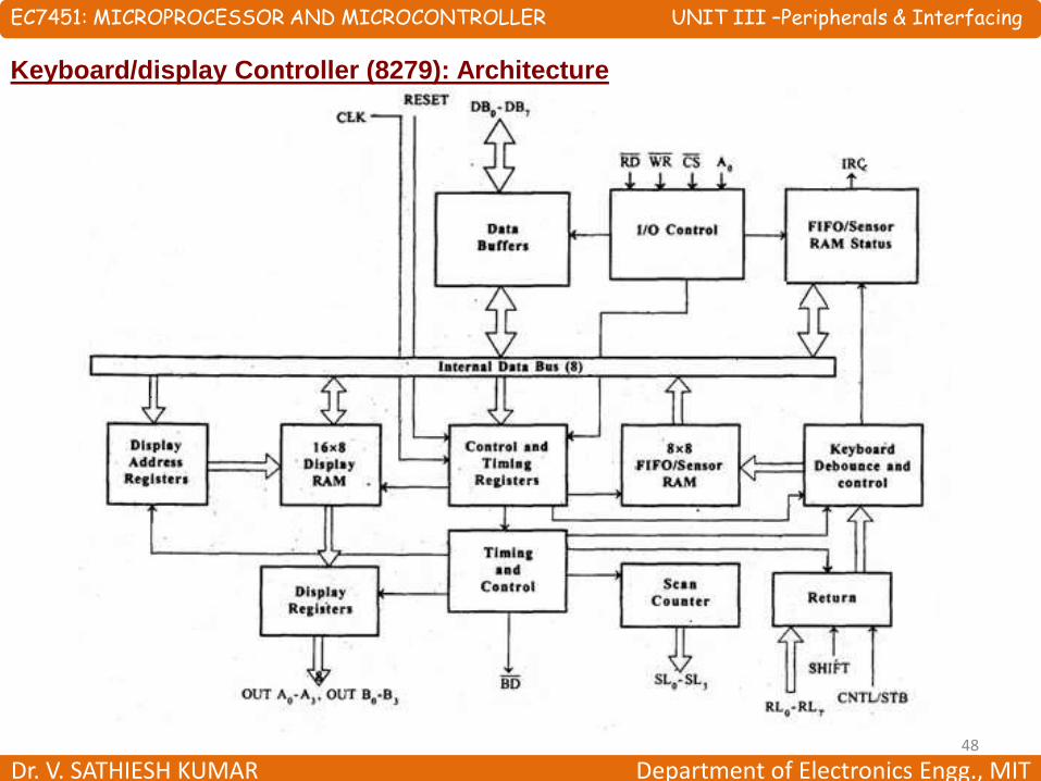
Keyboard/display Controller (8279): Architecture

EC7451: MICROPROCESSOR AND MICROCONTROLLER UNIT III –Peripherals & Interfacing
Dr. V. SATHIESH KUMAR Department of Electronics Engg., MIT 49
Keyboard/display Controller (8279): Architecture
I/O Control and Data Buffer:
•This unit controls the flow of data through the microprocessor.
•Its data buffer interfaces the external bus of the system with the internal bus of the
microprocessor.
•The pins A0, RD*, and WR* are used for command, status or data read/write
operations.
Control and Timing Register and Timing Control:
•This unit contains registers to store the keyboard, display modes, and other
operations as programmed by the CPU.
•The timing and control unit handles the timings for the operation of the circuit.

EC7451: MICROPROCESSOR AND MICROCONTROLLER UNIT III –Peripherals & Interfacing
Dr. V. SATHIESH KUMAR Department of Electronics Engg., MIT 50
Keyboard/display Controller (8279): Architecture
I/O Control and Data Buffer:
•This unit controls the flow of data through the microprocessor.
•Its data buffer interfaces the external bus of the system with the internal bus of the
microprocessor.
•The pins A0, RD*, and WR* are used for command, status or data read/write
operations.
Control and Timing Register and Timing Control:
•This unit contains registers to store the keyboard, display modes, and other
operations as programmed by the CPU.
•The timing and control unit handles the timings for the operation of the circuit.

EC7451: MICROPROCESSOR AND MICROCONTROLLER UNIT III –Peripherals & Interfacing
Dr. V. SATHIESH KUMAR Department of Electronics Engg., MIT 51
Keyboard/display Controller (8279): Architecture
Scan Counter:
•It has two modes i.e. Encoded mode and Decoded mode.
•In the encoded mode, the counter provides the binary count that is to be externally
decoded to provide the scan lines for the keyboard and display.
•In the decoded scan mode, the counter internally decodes the least significant 2
bits and provides a decoded 1 out of 4 scan on SL0-SL3.
Return Buffers, Keyboard Debounce, and Control:
•This unit first scans the key closure row-wise, if found then the keyboard debounce
unit debounces the key entry.
•In case, the same key is detected, then the code of that key is directly transferred
to the sensor RAM along with SHIFT & CONTROL key status.
EC7451: MICROPROCESSOR AND MICROCONTROLLER UNIT III –Peripherals & Interfacing
Dr. V. SATHIESH KUMAR Department of Electronics Engg., MIT 52
Keyboard/display Controller (8279): Architecture
FIFO/Sensor RAM and Status Logic:
•This unit acts as 8-byte first-in-first-out (FIFO) RAM where the key code of every
pressed key is entered into the RAM as per their sequence.
•The status logic generates an interrupt request after each FIFO read operation till
the FIFO gets empty.
•In the scanned sensor matrix mode, this unit acts as sensor RAM where its each
row is loaded with the status of their corresponding row of sensors into the matrix. When
the sensor changes its state, the IRQ line changes to high and interrupts the CPU.
Display Address Registers and Display RAM:
•This unit consists of display address registers which holds the addresses of the word
currently read/written by the CPU to/from the display RAM.

EC7451: MICROPROCESSOR AND MICROCONTROLLER UNIT III –Peripherals & Interfacing
Dr. V. SATHIESH KUMAR Department of Electronics Engg., MIT 53
Keyboard/display Controller (8279): Pin Details

EC7451: MICROPROCESSOR AND MICROCONTROLLER UNIT III –Peripherals & Interfacing
Dr. V. SATHIESH KUMAR Department of Electronics Engg., MIT 54
Keyboard/display Controller (8279): Pin Details
Data Bus Lines, DB0 - DB7: These are 8 bidirectional data bus lines used to transfer
the data to/from the CPU.
CLK: The clock input is used to generate internal timings required by the
microprocessor.
RESET: This pin is used to reset the microprocessor.
CS* Chip Select: When this pin is set to low, it allows read/write operations, else
this pin should be set to high.
A0: This pin indicates the transfer of command/status information. When it is low, it
indicates the transfer of data.
EC7451: MICROPROCESSOR AND MICROCONTROLLER UNIT III –Peripherals & Interfacing
Dr. V. SATHIESH KUMAR Department of Electronics Engg., MIT 55
Keyboard/display Controller (8279): Pin Details
RD*, WR* : This Read/Write pin enables the data buffer to send/receive data over the
data bus.
IRQ: This interrupt output line goes high when there is data in the FIFO sensor
RAM.
•The interrupt line goes low with each FIFO RAM read operation.
•However, if the FIFO RAM further contains any key-code entry to be read by the CPU,
this pin again goes high to generate an interrupt to the CPU.
Vss, Vcc : These are the ground and power supply lines of the microprocessor.
SL0 − SL3: These are the scan lines used to scan the keyboard matrix and display
the digits. These lines can be programmed as encoded or decoded, using the mode
control register.

EC7451: MICROPROCESSOR AND MICROCONTROLLER UNIT III –Peripherals & Interfacing
Dr. V. SATHIESH KUMAR Department of Electronics Engg., MIT 56
Keyboard/display Controller (8279): Pin Details
RL0 − RL7 : These are the Return Lines which are connected to one terminal of
keys, while the other terminal of the keys is connected to the decoded scan lines. These
lines are set to 0 when any key is pressed.
SHIFT: The Shift input line status is stored along with every key code in FIFO in the
scanned keyboard mode. Till it is pulled low with a key closure, it is pulled up internally
to keep it high
CNTL/STB - CONTROL/STROBED I/P Mode: In the keyboard mode, this line is used
as a control input and stored in FIFO on a key closure. The line is a strobe line that
enters the data into FIFO RAM, in the strobed input mode. It has an internal pull up.
The line is pulled down with a key closure.

EC7451: MICROPROCESSOR AND MICROCONTROLLER UNIT III –Peripherals & Interfacing
Dr. V. SATHIESH KUMAR Department of Electronics Engg., MIT 57
Keyboard/display Controller (8279): Pin Details
BD*: It stands for blank display. It is used to blank the display during digit
switching.
OUTA0 to OUTA3 and OUTB0 to OUTB3: These are the output ports for two 16x4 or
one 16x8 internal display refresh registers. The data from these lines is synchronized
with the scan lines to scan the display and the keyboard.
EC7451: MICROPROCESSOR AND MICROCONTROLLER UNIT III –Peripherals & Interfacing
Dr. V. SATHIESH KUMAR Department of Electronics Engg., MIT 58
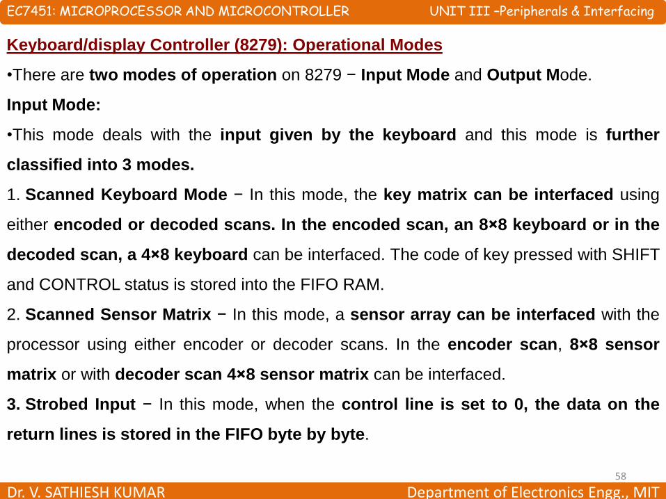
Keyboard/display Controller (8279): Operational Modes
•There are two modes of operation on 8279 − Input Mode and Output Mode.
Input Mode:
•This mode deals with the input given by the keyboard and this mode is further
classified into 3 modes.
1. Scanned Keyboard Mode − In this mode, the key matrix can be interfaced using
either encoded or decoded scans. In the encoded scan, an 8×8 keyboard or in the
decoded scan, a 4×8 keyboard can be interfaced. The code of key pressed with SHIFT
and CONTROL status is stored into the FIFO RAM.
2. Scanned Sensor Matrix − In this mode, a sensor array can be interfaced with the
processor using either encoder or decoder scans. In the encoder scan, 8×8 sensor
matrix or with decoder scan 4×8 sensor matrix can be interfaced.
3. Strobed Input − In this mode, when the control line is set to 0, the data on the
return lines is stored in the FIFO byte by byte.

EC7451: MICROPROCESSOR AND MICROCONTROLLER UNIT III –Peripherals & Interfacing
Dr. V. SATHIESH KUMAR Department of Electronics Engg., MIT 59
Keyboard/display Controller (8279): Operational Modes
Output Mode:
•This mode deals with display-related operations. This mode is further classified into
two output modes.
1. Display Scan − This mode allows 8/16 character multiplexed displays to be
organized as dual 4-bit/single 8-bit display units.
2. Display Entry − This mode allows the data to be entered for display either from
the right side/left side.

EC7451: MICROPROCESSOR AND MICROCONTROLLER UNIT III –Peripherals & Interfacing
Dr. V. SATHIESH KUMAR Department of Electronics Engg., MIT 60
Keyboard/display Controller : Decoded mode of operation
•In this mode, the matrix keyboard can have only four rows and eight columns.
•These four rows can be selected by using SL3-0 select lines.
•The eight columns can be selected using RL7-0 .
•So there are 4 * 8 = 32 keys.
•At the intersection of each row and column, there is a key.
•There are another two keys (Shift key and the Ctrl key), these two keys are not the
part of the matrix.

EC7451: MICROPROCESSOR AND MICROCONTROLLER UNIT III –Peripherals & Interfacing
Dr. V. SATHIESH KUMAR Department of Electronics Engg., MIT 61
Keyboard/display Controller : Decoded mode of operation
•In the decoded mode, the 8279 scans the keys by making logic 0 for each row at a
time, and then each of the eight columns is read.
•The following table is showing the pattern shown by the SL3-0 by 8279 for scanning
keyboard.
SL3-0
Row Being Scanned
1110
Row 0
1101
Row 1
1011
Row 2
0111
Row 3

EC7451: MICROPROCESSOR AND MICROCONTROLLER UNIT III –Peripherals & Interfacing
Dr. V. SATHIESH KUMAR Department of Electronics Engg., MIT 62
Keyboard/display Controller : Decoded mode of operation
•Let us see an example of this keyboard scanning mechanism.
•Let us consider that currently, it is scanning row 3 by sending the select line values
0111, and the received information is 10111111 from RL7-0.
•It is indicating that the RL6 is at logic 0.
•So for this data, the FIFO RAM will be loaded like below,
•The LS 3 bits indicating the column numbers (Here 110 means the column 6) and
next 3 bits are indicating the row number (Here 011 for row 3).
•As there are four rows in the keyboard so 2-bits are sufficient, but there are three bits
(One additional bit) for row selection.
Indicates Row 3 Indicates Column 6
Ctrl
Shift
0
1
1
1
1
0

EC7451: MICROPROCESSOR AND MICROCONTROLLER UNIT III –Peripherals & Interfacing
Dr. V. SATHIESH KUMAR Department of Electronics Engg., MIT 63
Keyboard/display Controller : Decoded mode of operation
•When the ctrl and shift buttons are not pressed, then these two fields will hold 1.
•After scanning the keyboard key, the IRQ is activated by 8279.
•This IRQ is connected with the Interrupt Request pin of the 8085.
•When the processor reads FIFO RAM, the IRQ pin becomes 0.
•When the processor is in disabled interrupt state, then the key content is stored into
the FIFO RAM.
•If another key is pressed in that time, that information is added after the previous key
information in FIFO RAM like a queue structure.
•Status Register: The status register is holding important information about the
FIFO RAM.

EC7451: MICROPROCESSOR AND MICROCONTROLLER UNIT III –Peripherals & Interfacing
Dr. V. SATHIESH KUMAR Department of Electronics Engg., MIT 64
Keyboard/display Controller : Decoded mode of operation
•The last three bits are used to represent the number of characters present in FIFO
RAM. It starts from 000 and incremented by 1.
•When one key data is sent by enabling the IRQ pin and the processor is reading the
content of FIFO RAM, then these values are decremented by 1.
•When the interrupts of the processor are disabled, and the user is pressing seven
keys, then the value of the last three bits will be 111.
•So if another key is pressed, the F flag will be set to 1, and three bits will become
000. This F flag will indicate the FIFO RAM is full.
•Now if another key is pressed when the FIFO RAM is full, it will overwrite the last
character of the FIFO RAM. It will generate an Over-run error. It will set the O flag.
•This O flag indicates the Over-run error.
•Similarly, when the F flag is 0, and the last three bits are also 000, then it indicates
that the FIFO RAM is not full and also it has no character to read.

EC7451: MICROPROCESSOR AND MICROCONTROLLER UNIT III –Peripherals & Interfacing
Dr. V. SATHIESH KUMAR Department of Electronics Engg., MIT 65
Keyboard/display Controller : Decoded mode of operation
•In this situation, if the processor is trying to read the FIFO RAM, it will generate
Underflow error by enabling the U flag.

EC7451: MICROPROCESSOR AND MICROCONTROLLER UNIT III –Peripherals & Interfacing
Dr. V. SATHIESH KUMAR Department of Electronics Engg., MIT 66
Keyboard/display Controller : Encoded mode of operation
•In most of the cases, the 8279 is used in Encoded mode of operation.
•In this mode, we can set eight rows and eight columns to connect 64 keys.
•Like the decoded mode, it also has shift and control key.
•So by adding these two with 64, there are 66 keys.

SL2-0
Row Being Scanned
000
Row 0
001
Row 1
010
Row 2
011
Row 3
100
Row 4
101
Row 5
110
Row 6
111
Row 7
EC7451: MICROPROCESSOR AND MICROCONTROLLER UNIT III –Peripherals & Interfacing
Dr. V. SATHIESH KUMAR Department of Electronics Engg., MIT 67
Keyboard/display Controller : Encoded mode of operation
•From this diagram, we can see that one external 3:8 decoder is used.
•To the decoder, the SL2-0 is connected. The SL3 is not used.
•The decoder output is connected with the eight rows of the matrix.
•The following table is showing the pattern shown by the SL2-0 by 8279 for scanning
keyboard.

EC7451: MICROPROCESSOR AND MICROCONTROLLER UNIT III –Peripherals & Interfacing
Dr. V. SATHIESH KUMAR Department of Electronics Engg., MIT 68
Keyboard/display Controller : Encoded mode of operation
•Let us see an example of this keyboard scanning mechanism.
•Let us consider that currently, it is scanning row 5 by sending the select line values
101, and the received information is 10111111 from RL7-0.
•It is indicating that the RL6 is at logic 0. So for this data, the FIFO RAM will be loaded
like below,
•The LS 3 bits are indicating the column numbers (Here 110 means the column 6)
and next3 bits are indicating the row number (Here 101 for row 5). Additional two
keys area are also present in the FIFO RAM.
Indicates Row 5 Indicates Column 6
Ctrl Shift 1 0 1 1 1 0

EC7451: MICROPROCESSOR AND MICROCONTROLLER UNIT III –Peripherals & Interfacing
Dr. V. SATHIESH KUMAR Department of Electronics Engg., MIT 69
Keyboard/display Controller : Interfacing with 8085 – I/O mapped I/O

EC7451: MICROPROCESSOR AND MICROCONTROLLER UNIT III –Peripherals & Interfacing
Dr. V. SATHIESH KUMAR Department of Electronics Engg., MIT 70
Keyboard/display Controller : Interfacing with 8085 – I/O mapped I/O
EC7451: MICROPROCESSOR AND MICROCONTROLLER UNIT III –Peripherals & Interfacing
Dr. V. SATHIESH KUMAR Department of Electronics Engg., MIT 71
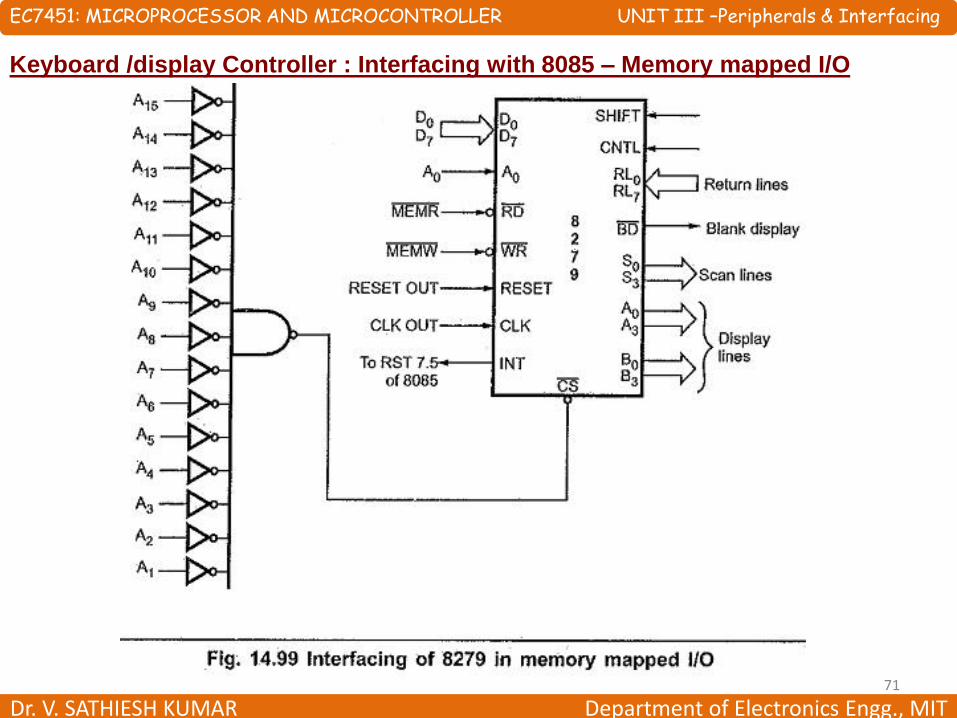
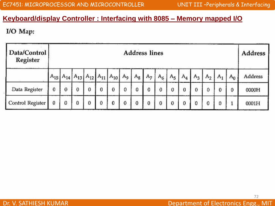
Keyboard /display Controller : Interfacing with 8085 – Memory mapped I/O
EC7451: MICROPROCESSOR AND MICROCONTROLLER UNIT III –Peripherals & Interfacing
Dr. V. SATHIESH KUMAR Department of Electronics Engg., MIT 72
Keyboard/display Controller : Interfacing with 8085 – Memory mapped I/O

EC7451: MICROPROCESSOR AND MICROCONTROLLER UNIT III –Peripherals & Interfacing
Dr. V. SATHIESH KUMAR Department of Electronics Engg., MIT 73
Keyboard/display Controller : Display interface
•The Intel 8279 is used for keyboard interfacing but it can also be used for multiplexed
7-segment LED display interfacing.
•To display a character into 7-segment display we have to store 7-segment code in
a display RAM location.
•The display RAM of this chip can store 16 bytes of data.
•To write to the display RAM one special command is needed to be applied on the
8279 control port.
•The following pattern is showing the RAM command that is written to the control port
of 8279.
•The first three bits are 100. It indicates ‘ Write to Display RAM’ command. The last
4-bits are AAAA. These are used to select the RAM location. The Ai bit is the auto-
increment bit.
1
0
0
Ai
A
A
A
A

EC7451: MICROPROCESSOR AND MICROCONTROLLER UNIT III –Peripherals & Interfacing
Dr. V. SATHIESH KUMAR Department of Electronics Engg., MIT 74
Keyboard/display Controller : Display interface
•To write at RAM location 4 in auto-increment mode, then the RAM pointer is
loaded with the address 4. When the processor writes to the display RAM for the first
time, it will be at RAM location 4. Then the address is incremented to 5 and so on.
•This following code achieves the objective of displaying ABCD in the address field.
MVI A, 10010100 // Common Anode 7Seg Display
OUT D1H //Write display location 4 in auto increment mode.
MVI A, A1H // dp g f e d c b a -> 1 0 1 0 0 0 0 1
OUT D0H //send A1H (‘d’) at RAM location 4
MVI A, C6H
OUT D0H //send C6H (‘C’) at RAM location 5
MVI A, 83H
OUT D0H //send 83H (‘b’) at RAM location 6
MVI A, 88H
OUT D0H //send 88H (‘A’) at RAM location 7

EC7451: MICROPROCESSOR AND MICROCONTROLLER UNIT III –Peripherals & Interfacing
Dr. V. SATHIESH KUMAR Department of Electronics Engg., MIT 75
Keyboard/display Controller : Display interface
•To read from any RAM location of 8279, one special command is needed to be
applied on the 8279 control port.
•The following pattern is showing the RAM command that is read from the control port
of 8279.
•The first three bits are 011. It indicates ‘Read from Display RAM’ command.
•The last 4-bits are AAAA. These are used to select the RAM location.
•The Ai bit is the auto-increment bit.
•The display RAM is the same for reading and writes operation.
0
1
1
Ai
A
A
A
A

EC7451: MICROPROCESSOR AND MICROCONTROLLER UNIT III –Peripherals & Interfacing
Dr. V. SATHIESH KUMAR Department of Electronics Engg., MIT 76
Keyboard/display Controller : Display interface
•As an example say we want to read from RAM location 4 in auto-increment mode,
then the RAM pointer is loaded with the address 4.
•If there are A1 and C6 are stored at RAM location 4 and 5, then the following code
achieves the objective of reading AB from the RAM.
MVI A, 01110100
OUT D1H //Read from display location 4 in auto increment mode.
IN D0H //Load A with A1, the address value is now pointing to 5
IN D0H //Load A with C6

EC7451: MICROPROCESSOR AND MICROCONTROLLER UNIT III –Peripherals & Interfacing
Dr. V. SATHIESH KUMAR Department of Electronics Engg., MIT 77
Keyboard/display Controller : Display interface
•There are two modes of 7-segment display operations. These modes are:
1. Decoded Mode of operation
2. Encoded Mode of operation
Decoded Mode of Operation:
•In this mode no external decoders are needed, one scan line is made logic 0 at a
time and this selects a particular LED position for the display purpose. In this
mode, four displays can be attached. The following table is showing the pattern
shown by the SL3-0 by 8279 for displays.
SL3-0 Selected LED
1110 LED 0
1101 LED 1
1011 LED 2
0111 LED 3

EC7451: MICROPROCESSOR AND MICROCONTROLLER UNIT III –Peripherals & Interfacing
Dr. V. SATHIESH KUMAR Department of Electronics Engg., MIT 78
Keyboard/display Controller : Display interface
•The following figure illustrates how to interface common anode 7-segment LED
displays in decoded mode.
•First of all, the 8279 chip outputs 1110 on SL3-0.This results in display 0 receiving the
5V power supply to its anode and all other LEDs are receiving 0V for their anodes.
•The contents of display RAM location 0 are output on A3-0 and B3-0 by the 8279.
•All of the displays are getting this information, but the character is displayed only
on the display-0 which receives the 5V power supply.
•Next, the select lines SL3-0 is loaded with 1101, so the second display will be selected
and the content of the display RAM has reflected the display.
•Thus the displays are showing different characters by refreshing the contents.

EC7451: MICROPROCESSOR AND MICROCONTROLLER UNIT III –Peripherals & Interfacing
Dr. V. SATHIESH KUMAR Department of Electronics Engg., MIT 79
Keyboard/display Controller : Display interface

EC7451: MICROPROCESSOR AND MICROCONTROLLER UNIT III –Peripherals & Interfacing
Dr. V. SATHIESH KUMAR Department of Electronics Engg., MIT 80
Keyboard/display Controller : Display interface
Encoded Mode of Operation:
•We can connect at most 16 displays.
•Here external decoders are needed.
•This mode can be used for 8-character or 16-character display.
•For 8-character display, only SL2-0 pins are used. The SL3 is unused.
•For 16-character display, all of the select lines are used.
•The following figure illustrates how to interface common anode 7-segment LED
displays in encoded mode.
•In this diagram, we are assuming that 16-displays are connected.
•In this case, the SL3-0 values are changing from 0000 to 1111, so only the selected
display is getting the 5V power supply in its anode, and others are getting 0V.
•The select lines SL3-0 is loaded with 1101, so the second display will be selected and
the content of the display RAM has reflected the display. Thus the displays are showing
different characters by refreshing the contents.

EC7451: MICROPROCESSOR AND MICROCONTROLLER UNIT III –Peripherals & Interfacing
Dr. V. SATHIESH KUMAR Department of Electronics Engg., MIT 81
Keyboard/display Controller : Display interface

EC7451: MICROPROCESSOR AND MICROCONTROLLER UNIT III –Peripherals & Interfacing
Dr. V. SATHIESH KUMAR Department of Electronics Engg., MIT 82
Keyboard/display Controller : Mode Settings
•This command (000) is used to program operating modes of keyboard and display.
• Three least significant bits decide the keyboard mode and next two bits decide
the display mode, as shown in the tables.

EC7451: MICROPROCESSOR AND MICROCONTROLLER UNIT III –Peripherals & Interfacing
Dr. V. SATHIESH KUMAR Department of Electronics Engg., MIT 83
Keyboard/display Controller : Mode Settings
• The keys are automatically debounced. The two operating modes of keyboard section
are 2-key lockout and N-key rollover.
•In the 2-key lockout mode, if two keys are pressed simultaneously, only the first key is
recognized.
•In the N-key rollover mode, simultaneous keys are recognized and their codes are
stored in FIFO.

EC7451: MICROPROCESSOR AND MICROCONTROLLER UNIT III –Peripherals & Interfacing
Dr. V. SATHIESH KUMAR Department of Electronics Engg., MIT 84
Keyboard/display Controller : Mode Settings

EC7451: MICROPROCESSOR AND MICROCONTROLLER UNIT III –Peripherals & Interfacing
Dr. V. SATHIESH KUMAR Department of Electronics Engg., MIT 85
Keyboard/display Controller : Mode Settings
16th

EC7451: MICROPROCESSOR AND MICROCONTROLLER UNIT III –Peripherals & Interfacing
Dr. V. SATHIESH KUMAR Department of Electronics Engg., MIT 86
Keyboard/display Controller : Mode Settings

EC7451: MICROPROCESSOR AND MICROCONTROLLER UNIT III –Peripherals & Interfacing
Dr. V. SATHIESH KUMAR Department of Electronics Engg., MIT 87
Programmable Timer Controller (8253/8254) :
•The Intel 8253 and 8254 are Programmable Interval Timers (PTIs) designed for
microprocessors to perform timing and counting functions using three 16-bit
registers.
•Each counter has 2 input pins, i.e. Clock and Gate, and 1 pin for “OUT” output.
•To operate a counter, a 16-bit count is loaded in its register.
•On command, it begins to decrement the count until it reaches 0, then it generates
a pulse that can be used to interrupt the CPU.
8253 8254
Its operating frequency is 0 - 2.6 MHz Its operating frequency is 0 - 10 MHz
It uses N-MOS technology It uses H-MOS technology
Read-Back command is not available Read-Back command is available
Reads and writes of the same counter cannot be interleaved.
Reads and writes of the same counter can be interleaved.

EC7451: MICROPROCESSOR AND MICROCONTROLLER UNIT III –Peripherals & Interfacing
Dr. V. SATHIESH KUMAR Department of Electronics Engg., MIT 88
Programmable Timer Controller (8253/8254) :
•The most prominent features of 8253/54 are as follows,
1.It has three independent 16-bit down counters.
2.It can handle inputs from DC to 10 MHz
3.These three counters can be programmed for either binary or BCD count.
4.It is compatible with almost all microprocessors.
5.8254 has a powerful command called READ BACK command, which allows the
user to check the count value, the programmed mode, the current mode, and the
current status of the counter.

EC7451: MICROPROCESSOR AND MICROCONTROLLER UNIT III –Peripherals & Interfacing
Dr. V. SATHIESH KUMAR Department of Electronics Engg., MIT 89
Programmable Timer Controller (8253/8254) : Architecture
EC7451: MICROPROCESSOR AND MICROCONTROLLER UNIT III –Peripherals & Interfacing
Dr. V. SATHIESH KUMAR Department of Electronics Engg., MIT 90
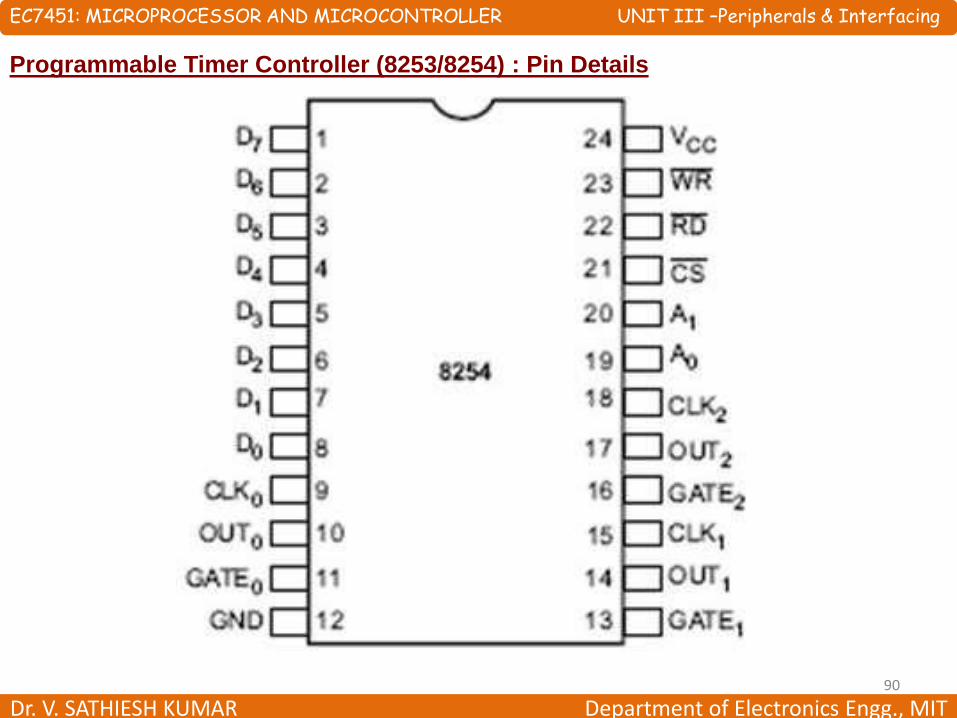
Programmable Timer Controller (8253/8254) : Pin Details

EC7451: MICROPROCESSOR AND MICROCONTROLLER UNIT III –Peripherals & Interfacing
Dr. V. SATHIESH KUMAR Department of Electronics Engg., MIT 91
Programmable Timer Controller (8253/8254) : Pin Details
•There are three counters, a data bus buffer, Read/Write control logic, and a
control register.
•Each counter has two input signals - CLOCK & GATE, and one output signal - OUT.
Data Bus Buffer:
•It is a tri-state, bi-directional, 8-bit buffer, which is used to interface the 8253/54 to
the system data bus.
•It has three basic functions,
1. Programming the modes of 8253/54:
2. Loading the count registers.
3. Reading the count values.

EC7451: MICROPROCESSOR AND MICROCONTROLLER UNIT III –Peripherals & Interfacing
Dr. V. SATHIESH KUMAR Department of Electronics Engg., MIT 92
Programmable Timer Controller (8253/8254) : Pin Details
Read/Write Logic:
•It includes 5 signals, i.e. RD*, WR*, CS*, and the address lines A0 and A1.
•In the peripheral I/O mode, the RD* and WR* signals are connected to IOR* and
IOW*, respectively.
•In the memory-mapped I/O mode, these are connected to MEMR* and MEMW*.
•Address lines A0 and A1 of the CPU are connected to lines A0 and A1 of the 8253/54,
and CS* is tied to a decoded address.
•The control word register and counters are selected according to the signals on lines
A0 and A1.
A1 A0 Result
0 0 Counter 0
0 1 Counter 1
1 0 Counter 2
1 1 Control Word Register
X X No Selection

EC7451: MICROPROCESSOR AND MICROCONTROLLER UNIT III –Peripherals & Interfacing
Dr. V. SATHIESH KUMAR Department of Electronics Engg., MIT 93
Programmable Timer Controller (8253/8254) : Pin Details
Control Word Register:
•This register is accessed when lines A0 and A1 are at logic 1.
•It is used to write a command word, which specifies the counter to be used, its
mode, and either a read or write operation.
A1 A0 RD* WR* CS* Result
0 0 1 0 0 Write Counter 0
0 1 1 0 0 Write Counter 1
1 0 1 0 0 Write Counter 2
1 1 1 0 0 Write Control Word
0 0 0 1 0 Read Counter 0
0 1 0 1 0 Read Counter 1
1 0 0 1 0 Read Counter 2
1 1 0 1 0 No operation
X X 1 1 0 No operation
X X X X 1 No operation
EC7451: MICROPROCESSOR AND MICROCONTROLLER UNIT III –Peripherals & Interfacing
Dr. V. SATHIESH KUMAR Department of Electronics Engg., MIT 94
Programmable Timer Controller (8253/8254) :
Counters
•Each counter consists of a single, 16 bit-down counter, which can be operated in
either binary or BCD.
•Its input and output is configured by the selection of modes stored in the control
word register.
•The programmer can read the contents of any of the three counters without
disturbing the actual count in process.

EC7451: MICROPROCESSOR AND MICROCONTROLLER UNIT III –Peripherals & Interfacing
Dr. V. SATHIESH KUMAR Department of Electronics Engg., MIT 95
Programmable Timer Controller (8253/8254) : Internal Architecture of a Counter
•To each counter, there is a corresponding background counter, denoted as BCounter.
•The counter loads the BCounter at the appropriate moment depending on the mode
of operation of the counter.
•The counter value remains unchanged even when the clock pulses occur.
•It is only the BCounter that is decremented for every clock pulse.
•BCounter is affected by the gate input depending on the mode of operation of the
counter.

EC7451: MICROPROCESSOR AND MICROCONTROLLER UNIT III –Peripherals & Interfacing
Dr. V. SATHIESH KUMAR Department of Electronics Engg., MIT 96
Programmable Timer Controller (8253/8254) :
•Some important facts of this chip.
1. When the chip is powering up, the state is undefined. The mode, count value, and
outputs are undefined in that time.
2. Each counter must be programmed before it is used. We do not need to program
some unused counters.
3. Counters are programmed by writing the control words and then one initial
count.
• The structure of the counter is like this:
7
6
5
4
3
2
1
0
SC1
SC0
RW1
RW0
M2
M1
M0
BCD/Binary

EC7451: MICROPROCESSOR AND MICROCONTROLLER UNIT III –Peripherals & Interfacing
Dr. V. SATHIESH KUMAR Department of Electronics Engg., MIT 97
Programmable Timer Controller (8253/8254) :
•We can select the counter by the SC1 and SC0.
• The values of the RW1 and RW0 are used to denote the read and write operation.
SC1 SC0 Selection
0 0 Counter 0
0 1 Counter 1
1 0 Counter 2
1 1 Read the back status
RW1 RW0 Selection
0 0 Read on the fly for read operation. It is illegal for write operation
0 1 Read or Write the lower byte
1 0 Read or Write the upper byte
1 1 Read or Write lower byte followed by upper byte

EC7451: MICROPROCESSOR AND MICROCONTROLLER UNIT III –Peripherals & Interfacing
Dr. V. SATHIESH KUMAR Department of Electronics Engg., MIT 98
Programmable Timer Controller (8253/8254) :
•Three bits of M2, M1 and M0 are used to decide programming modes.
•The last bit (LSB) of the control word is used to select whether the counting will be
in Binary or BCD. If this is 0, it will act like binary counter, otherwise it will act like
BCD counter.
M2 M1 M0 Operating Mode
0 0 0 Mode 0
0 0 1 Mode 1
X 1 0 Mode 2
X 1 1 Mode 3
1 0 0 Mode 4
1 0 1 Mode 5

EC7451: MICROPROCESSOR AND MICROCONTROLLER UNIT III –Peripherals & Interfacing
Dr. V. SATHIESH KUMAR Department of Electronics Engg., MIT 99
Programmable Timer Controller (8253/8254) : Operational Modes
•8253/54 can be operated in 6 different modes.
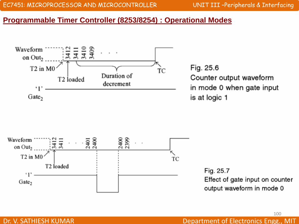
1. Mode 0 ─ Interrupt on Terminal Count:
•It is used to generate an interrupt to the microprocessor after a certain interval.
•Initially the output is low after the mode is set. The output remains LOW after the count
value is loaded into the counter. The process of decrementing the counter continues till
the terminal count is reached, i.e., the count become zero and the output goes HIGH
and will remain high until it reloads a new count.
•The GATE signal is high for normal counting. When GATE goes low, counting is
terminated and the current count is latched till the GATE goes high again.
•Let us say, it is desired to have Counter2 operate in mode 0 with a count value of
3412 decimal.
•If the Clock2 frequency is 1 MHz, the Out2 pin becomes logic 1 after 3412 us.
EC7451: MICROPROCESSOR AND MICROCONTROLLER UNIT III –Peripherals & Interfacing
Dr. V. SATHIESH KUMAR Department of Electronics Engg., MIT 100
Programmable Timer Controller (8253/8254) : Operational Modes

EC7451: MICROPROCESSOR AND MICROCONTROLLER UNIT III –Peripherals & Interfacing
Dr. V. SATHIESH KUMAR Department of Electronics Engg., MIT 101
Programmable Timer Controller (8253/8254) : Operational Modes
2. Mode 1 – Programmable One Shot:
•It can be used as a monostable multi-vibrator (generates an output low pulse).
•The stable state of the multi-vibrator in this mode is logic 1.
•The gate input is used as a trigger input in this mode.
•When a trigger pulse occurs on the gate input, the multi-vibrator output goes to
logic 0 state, which is the quasi-stable state.
•It remains in this state for a duration dependent on the loaded counter value and
the clock frequency. Then it reverts to the stable state of logic 1.
EC7451: MICROPROCESSOR AND MICROCONTROLLER UNIT III –Peripherals & Interfacing
Dr. V. SATHIESH KUMAR Department of Electronics Engg., MIT 102
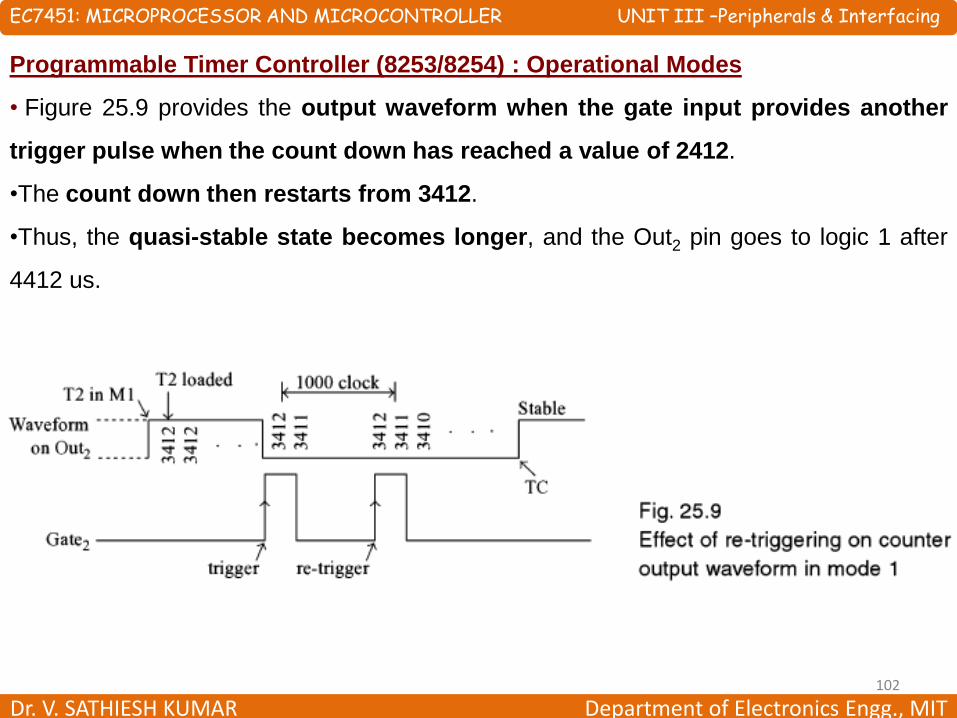
Programmable Timer Controller (8253/8254) : Operational Modes
• Figure 25.9 provides the output waveform when the gate input provides another
trigger pulse when the count down has reached a value of 2412.
•The count down then restarts from 3412.
•Thus, the quasi-stable state becomes longer, and the Out2 pin goes to logic 1 after
4412 us.
EC7451: MICROPROCESSOR AND MICROCONTROLLER UNIT III –Peripherals & Interfacing
Dr. V. SATHIESH KUMAR Department of Electronics Engg., MIT 103
Programmable Timer Controller (8253/8254) : Operational Modes
3. Mode 2 – Rate Generator:
•The output is normally high after initialization.
•Whenever the count becomes zero, another low pulse (for one input clock period)
is generated at the output and the counter will be reloaded.
•In software synchronization, the gate input is held at logic 1 throughout.
•The moment the counter is loaded by the processor, the BCounter is loaded from
the counter and the countdown operation starts.
•During the last count, the output becomes logic 0 for one input clock period.
•Then the BCounter is reloaded from counter value, and the count down operation
continues with the output at logic 1.
•Later, even if the gate input is made logic 0, the count down continues and
generates a pulse during the last count and the operation stops.

EC7451: MICROPROCESSOR AND MICROCONTROLLER UNIT III –Peripherals & Interfacing
Dr. V. SATHIESH KUMAR Department of Electronics Engg., MIT 104
Programmable Timer Controller (8253/8254) : Operational Modes
•In hardware synchronization, the gate input is held at logic 0 initially.
•Then, the BCounter is not loaded from the counter even when the processor loads
the counter.
•Only when the gate input makes a 0 to 1 transition, the BCounter is loaded from
counter and the count down operation begins.
•During the last count, the output becomes logic 0 for one input clock period.
•Then the BCounter is reloaded from counter value, and the count down operation
continues with the output at logic 1.

EC7451: MICROPROCESSOR AND MICROCONTROLLER UNIT III –Peripherals & Interfacing
Dr. V. SATHIESH KUMAR Department of Electronics Engg., MIT 105
Programmable Timer Controller (8253/8254) : Operational Modes
• Later, even if the gate input is made logic 0, the count down continues and
generates a pulse during the last count and the operation stops.

EC7451: MICROPROCESSOR AND MICROCONTROLLER UNIT III –Peripherals & Interfacing
Dr. V. SATHIESH KUMAR Department of Electronics Engg., MIT 106
Programmable Timer Controller (8253/8254) : Operational Modes
4. Mode 3 – Square Wave Generator:
•This mode is similar to Mode 2 except the output remains low for half of the timer
period and high for the other half of the period.
• In software synchronization, the gate input is held at logic 1 throughout.
•The moment the counter is loaded by the processor, the BCounter is loaded from the
counter and the count-down operation begins.
•The output will be in logic 1 for 50% of the time and logic 0 for the remaining 50% of
count down time.

EC7451: MICROPROCESSOR AND MICROCONTROLLER UNIT III –Peripherals & Interfacing
Dr. V. SATHIESH KUMAR Department of Electronics Engg., MIT 107
Programmable Timer Controller (8253/8254) : Operational Modes
• In hardware synchronization, the gate input is held at logic 0 initially.
•Then, even when the processor loads the counter, the BCounter is not loaded from the
counter.
•It is loaded from the counter and counter down operation begins only when the gate
input makes a 0 to 1 transition.
•The output will be in logic 1 for 50% of the time and logic 0 for the remaining 50% of
count down time.

EC7451: MICROPROCESSOR AND MICROCONTROLLER UNIT III –Peripherals & Interfacing
Dr. V. SATHIESH KUMAR Department of Electronics Engg., MIT 108
Programmable Timer Controller (8253/8254) : Operational Modes
5. Mode 4 − Software Triggered Mode:
•In this mode, the output will remain high until the timer has counted to zero, at
which point the output will pulse low and then go high again.
•The count is latched when the GATE signal goes LOW.
•On the terminal count (TC), the output goes low for one clock cycle then goes
HIGH. This low pulse can be used as a strobe.

EC7451: MICROPROCESSOR AND MICROCONTROLLER UNIT III –Peripherals & Interfacing
Dr. V. SATHIESH KUMAR Department of Electronics Engg., MIT 109
Programmable Timer Controller (8253/8254) : Operational Modes
6. Mode 5 – Hardware Triggered Mode:
•This mode generates a strobe in response to an externally generated signal.
•This mode is similar to mode 4 except that the counting is initiated by a signal at the
gate input, which means it is hardware triggered instead of software triggered.
•After it is initialized, the output goes high.
•When the terminal count is reached, the output goes low for one clock cycle.

EC7451: MICROPROCESSOR AND MICROCONTROLLER UNIT III –Peripherals & Interfacing
Dr. V. SATHIESH KUMAR Department of Electronics Engg., MIT 110
Programmable Interrupt Controller (8259) :
•In 8085 and 8086 there are five hardware interrupts (TRAP, RST 7.5, RST 6.5, RST
5.5, INTR) and two hardware interrupts (NMI, INTR), respectively.
•By adding 8259, we can increase the interrupt handling capability.
•This chip combines the multi-interrupt input source to single interrupt output.
•This provides 8-interrupts from IR0 to IR7.
•Let us see some features of this IC:
1. This chip is designed for 8085 and 8086.
2. It can be programmed either in edge triggered, or in level triggered mode
3. We can mask individual bits of Interrupt Request Register.
4. By cascading 8259 chips, we can increase interrupts up to 64 interrupt lines
5. Clock cycle is not needed.

EC7451: MICROPROCESSOR AND MICROCONTROLLER UNIT III –Peripherals & Interfacing
Dr. V. SATHIESH KUMAR Department of Electronics Engg., MIT 111
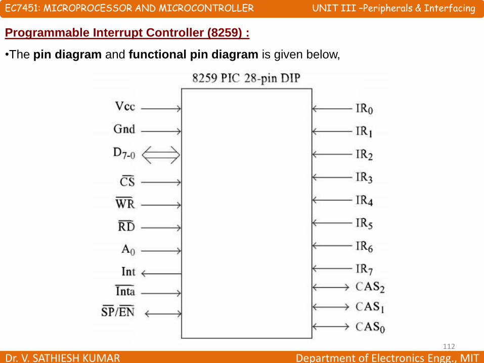
Programmable Interrupt Controller (8259) :
•The pin diagram and functional pin diagram is given below,
EC7451: MICROPROCESSOR AND MICROCONTROLLER UNIT III –Peripherals & Interfacing
Dr. V. SATHIESH KUMAR Department of Electronics Engg., MIT 112
Programmable Interrupt Controller (8259) :
•The pin diagram and functional pin diagram is given below,

EC7451: MICROPROCESSOR AND MICROCONTROLLER UNIT III –Peripherals & Interfacing
Dr. V. SATHIESH KUMAR Department of Electronics Engg., MIT 113
Programmable Interrupt Controller (8259) :
•The block diagram is given below,

EC7451: MICROPROCESSOR AND MICROCONTROLLER UNIT III –Peripherals & Interfacing
Dr. V. SATHIESH KUMAR Department of Electronics Engg., MIT 114
Programmable Interrupt Controller (8259) :
Block Description
Data Bus Buffer
This block is used to communicate between 8259 and 8085/8086
by acting as buffer.
It gets the control word from 8085/8086 and send it to the
8259.
It transfers the opcode of the selected interrupts and address
of ISR to the other connected microprocessor. It can send
maximum 8-bit at a time.
R*/W* Control
Logic
This block functions when the value of pin CS is 0. This block is
used to flow the data depending upon the inputs of RD* and WR*.
These are active low pins for read and write.

EC7451: MICROPROCESSOR AND MICROCONTROLLER UNIT III –Peripherals & Interfacing
Dr. V. SATHIESH KUMAR Department of Electronics Engg., MIT 115
Programmable Interrupt Controller (8259) :
Block Description
Control Logic
It controls the functionality of each block.
It has pin called INT. This is connected to other microprocessors
for taking the interrupt request.
If 8259 is enabled, and also the interrupt flags of other
microprocessors are high then this causes the value of the output
INT pin high, and in this way this chip can responds requests made
by other microprocessors.
Interrupt Request
Register
It stores all interrupt level that are requesting for interrupt
service.
Interrupt Service
Register
It stores interrupt level that are currently being execute.

EC7451: MICROPROCESSOR AND MICROCONTROLLER UNIT III –Peripherals & Interfacing
Dr. V. SATHIESH KUMAR Department of Electronics Engg., MIT 116
Programmable Interrupt Controller (8259) :
Block Description
Interrupt Mask
Register
It stores interrupt level that will be masked, by storing the
masking bits of interrupt level.
Priority Resolver
It checks all three registers, and set the priority of the
interrupts.
Interrupt with the highest priority is set in the ISR register.
It also reset the interrupt level which is already been serviced
in the IRR.
Cascade Buffer
To increase number of interrupt pin, we can cascade more
number of pins, by using cascade buffer. When we are going to
increase the interrupt capability, CSA lines are used to control
multiple interrupts.
EC7451: MICROPROCESSOR AND MICROCONTROLLER UNIT III –Peripherals & Interfacing
Dr. V. SATHIESH KUMAR Department of Electronics Engg., MIT 117
Programmable Interrupt Controller (8259) :
•The 8259 accepts interrupt requests from as many as eight interrupting devices
on IR0 to IR7 pins.
•Then it identifies the highest priority interrupt request from among those inputs
that are active.
•It is possible to configure the 8259 for ‘fixed priority’ mode of operation.
•In such a case, IR0 has the highest and IR7 has the lowest priority.
•The details about the interrupt requests that are active are stored in the interrupt
request register (IRR).
•It is possible to mask the interrupt requests by loading the interrupt mask register
(IMR).
•Information about the interrupt requests that are presently being serviced will be
kept in in-service register (ISR).

EC7451: MICROPROCESSOR AND MICROCONTROLLER UNIT III –Peripherals & Interfacing
Dr. V. SATHIESH KUMAR Department of Electronics Engg., MIT 118
Programmable Interrupt Controller (8259) :
•There is a priority resolver unit in the 8259.
•It receives inputs from IRR, IMR and ISR and identifies the highest priority
interrupt request.
•If IR4 and IR5 are activated simultaneously. As the priority of IR4 is greater than IR5
that is currently being serviced, the INT (interrupt request) output is activated.
•At the same time, bit 4 of ISR is set to 1 by the 8259.
•The INT output of 8259 is connected to INTR input of 8085.
•The INT output of 8259 should not be connected to any other interrupt pin of 8085.

EC7451: MICROPROCESSOR AND MICROCONTROLLER UNIT III –Peripherals & Interfacing
Dr. V. SATHIESH KUMAR Department of Electronics Engg., MIT 119
Programmable Interrupt Controller (8259) :

EC7451: MICROPROCESSOR AND MICROCONTROLLER UNIT III –Peripherals & Interfacing
Dr. V. SATHIESH KUMAR Department of Electronics Engg., MIT 120
Programmable Interrupt Controller (8259) :
•The priority resolver decides to activate INT output only when the following
conditions are met,
1. An IR input is activated.
2. The IR input is not masked.
3. The processor is presently not servicing an IR request with a higher priority.
•The 8085 completes the execution of the instruction during which the INTR input
was activated.
•Then the 8085 sends out INTA* output thrice in succession assuming that the 8085
interrupt system is enabled, and the higher priority interrupts of 8085 are not
active.
•In response to the activation of INTA*, the 8259 sends to the 8085 using the D7 – D0
pins a 3-byte CALL instruction.

EC7451: MICROPROCESSOR AND MICROCONTROLLER UNIT III –Peripherals & Interfacing
Dr. V. SATHIESH KUMAR Department of Electronics Engg., MIT 121
Programmable Interrupt Controller (8259) :
•The first time the INTA* is activated, the 8259 sends code for CALL (=CDH) to the
8085 on D7 – D0 pins. It is received in the IR register of 8085.
•The second time the INTA* is activated the 8259 sends LS byte of the interrupt
vector (IV) address to the 8085 on D7 – D0 pins. It is received in the Z register of
8085.
•The third time the INTA* is activated, the 8259 sends MS byte of IV address to the
8085 on D7 – D0 pins. It is received in the W register of 8085.
•The IV address supplied by the 8259 to the 8085 depends on the IR input of 8259 that
is being serviced. This results in a branch to the appropriate ISS.
•After finishing the ISS, the control returns to the main program.
•Note: The processor is not required to identify the source of the interrupt on INTR pin.
•8259 could also be configured for ‘rotating priority mode’.

EC7451: MICROPROCESSOR AND MICROCONTROLLER UNIT III –Peripherals & Interfacing
Dr. V. SATHIESH KUMAR Department of Electronics Engg., MIT 122
Programmable Interrupt Controller (8259) :

EC7451: MICROPROCESSOR AND MICROCONTROLLER UNIT III –Peripherals & Interfacing
Dr. V. SATHIESH KUMAR Department of Electronics Engg., MIT 123
Serial Communication Interface (8251) :
•The 8251 chip is Universal Synchronous Asynchronous Receiver Transmitter
(USART).
• It acts as a mediator between the microprocessor and peripheral devices.
•It converts serial data to parallel form and vice versa.
1.It takes data serially from peripheral (outside devices) and converts into parallel data.
2.After converting the data into parallel form, it transmits it to the CPU.
3.Similarly, it receives parallel data from microprocessor and converts it into serial form.
4.After converting data into serial form, it transmits it to outside device (peripheral).
•This chip is 28 pin DIP.

EC7451: MICROPROCESSOR AND MICROCONTROLLER UNIT III –Peripherals & Interfacing
Dr. V. SATHIESH KUMAR Department of Electronics Engg., MIT 124
Serial Communication Interface (8251) : Pin Description

EC7451: MICROPROCESSOR AND MICROCONTROLLER UNIT III –Peripherals & Interfacing
Dr. V. SATHIESH KUMAR Department of Electronics Engg., MIT 125
Serial Communication Interface (8251) :
Pin Description
D0 – D7 Parallel data
C/D* Control register or Data buffer select
RD* Read Control
WR* Write control
CS* Chip Select
CLK Clock pulse
RESET Reset
TxC* Transmitter Clock
TxD Transmitted data
RxC* Receiver Clock
RxD Receiver Data

EC7451: MICROPROCESSOR AND MICROCONTROLLER UNIT III –Peripherals & Interfacing
Dr. V. SATHIESH KUMAR Department of Electronics Engg., MIT 126
Serial Communication Interface (8251) :
Pin Description
RxRDY Receiver Ready
TxRDY Transmitter Ready
DSR* Data Set Ready
DTR* Data Terminal Ready
SYNDET/BRKDET Synchronous Detect/Detect Break
RTS* Request to send Data
CTS* Clear to send Data
TxEMPTY Transmitter Empty
Vcc Vcc (5V)
GND Ground(0V)

EC7451: MICROPROCESSOR AND MICROCONTROLLER UNIT III –Peripherals & Interfacing
Dr. V. SATHIESH KUMAR Department of Electronics Engg., MIT 127
Serial Communication Interface (8251) : Functional Block Diagram

EC7451: MICROPROCESSOR AND MICROCONTROLLER UNIT III –Peripherals & Interfacing
Dr. V. SATHIESH KUMAR Department of Electronics Engg., MIT 128
Serial Communication Interface (8251) :
•There are five different sections in 8251,
1. Read/ Write control logic
2. Transmitter
3. Receiver
4. Data Bus Buffer
5. Modem Control.
•Data bus buffer: This block helps in interfacing the internal data bus of 8251 to the
system data bus. The data transmission is possible between 8251 and CPU by the
data bus buffer block.

EC7451: MICROPROCESSOR AND MICROCONTROLLER UNIT III –Peripherals & Interfacing
Dr. V. SATHIESH KUMAR Department of Electronics Engg., MIT 129
Serial Communication Interface (8251) :
•Read/Write control logic: It is a control block for overall device. The operation
selection depends upon input signals as,
• In this way, this unit selects one of the three registers- data buffer register, control
register, status register.
EC7451: MICROPROCESSOR AND MICROCONTROLLER UNIT III –Peripherals & Interfacing
Dr. V. SATHIESH KUMAR Department of Electronics Engg., MIT 130
Serial Communication Interface (8251) :
•Modem control (modulator/demodulator): A device converts analog signals to
digital signals and vice-versa and helps the computers to communicate over
telephone lines or cable wires.
The following are active-low pins of Modem.
DSR*: Data Set Ready signal is an input signal.
DTR*: Data terminal Ready is an output signal.
CTS*: It is an input signal which controls the data transmit circuit.
RTS*: It is an output signal which is used to set the status RTS.
•Transmit buffer: This block is used for parallel to serial converter that receives a
parallel byte for conversion into serial signal and further transmission onto the common
channel.
TXD: It is an output signal, if its value is one, means transmitter will transmit the
data.

EC7451: MICROPROCESSOR AND MICROCONTROLLER UNIT III –Peripherals & Interfacing
Dr. V. SATHIESH KUMAR Department of Electronics Engg., MIT 131
Serial Communication Interface (8251) :
•Transmit control: This block is used to control the data transmission with the help of
following pins:
TXRDY: It means transmitter is ready to transmit data character.
TXEMPTY: An output signal which indicates that TXEMPTY pin has transmitted all
the data characters and transmitter is empty now.
TXC: An active-low input pin which controls the data transmission rate of
transmitted data.
•Receive buffer: This block acts as a buffer for the received data.
RXD: An input signal which receives the data.

EC7451: MICROPROCESSOR AND MICROCONTROLLER UNIT III –Peripherals & Interfacing
Dr. V. SATHIESH KUMAR Department of Electronics Engg., MIT 132
Serial Communication Interface (8251) :
•Receive control: This block controls the receiving data.
RXRDY: An input signal indicates that it is ready to receive the data.
RXC: An active-low input signal which controls the data transmission rate of
received data.
SYNDET/BD: An input or output terminal. External synchronous mode-input
terminal and asynchronous mode-output terminal.

EC7451: MICROPROCESSOR AND MICROCONTROLLER UNIT III –Peripherals & Interfacing
Dr. V. SATHIESH KUMAR Department of Electronics Engg., MIT 133
Serial Communication Interface (8251) : Interfacing with 8085
• Now let us see how 8251 can be interfaced with 8085.
•In the diagram, we can see that eight data lines D7-0 are connected to the data bus of
the microprocessor.
•Also the RD* and WR* of the 8251 are also connected with the RD* and WR* of 8051.
•The 8251 is getting the clock from the CLK OUT pin of 8085.
•And the RESET is also connected to the RESET OUT pin of the microprocessor.
•The C/D* pin is used to select either control register or data register. This pin is
connected to the A0 pin of 8085.
•The CS* pin of 8251 is attached to the output of an address decoder circuit.
•The address decoder uses A7 to A1 lines of the microprocessor.
•In this diagram the CS* will be enabled when A7 and A4 is at logic 1, and all other lines
are at logic 0.

EC7451: MICROPROCESSOR AND MICROCONTROLLER UNIT III –Peripherals & Interfacing
Dr. V. SATHIESH KUMAR Department of Electronics Engg., MIT 134
Serial Communication Interface (8251) :

EC7451: MICROPROCESSOR AND MICROCONTROLLER UNIT III –Peripherals & Interfacing
Dr. V. SATHIESH KUMAR Department of Electronics Engg., MIT 135
Serial Communication Interface (8251) :
From the following table, we can see how to read or write data word, read the status
word and write control word.
A0 RD* WR* Task Port Address
0 0 1 Read Data Word 90H
0 1 0 Write Data Word 90H
1 0 1 Read Status Word 91H
1 1 0 Write Control Word 91H
EC7451: MICROPROCESSOR AND MICROCONTROLLER UNIT III –Peripherals & Interfacing
Dr. V. SATHIESH KUMAR Department of Electronics Engg., MIT 136
Summary:
1. Programmable Peripheral Interface (8255)
2. Keyboard display controller (8279)
3. ADC0808 and DAC0808 Interface
4. Programmable Timer Controller (8254)
5. Programmable interrupt controller (8259)
6. Serial Communication Interface (8251)