ec2303-computer architecture and organization question ... · pdf fileec2303-computer...
TRANSCRIPT
DHANALAKSHMI SRINIVASAN INSTITUTE OF RESEARCH AND TECHNOLOGY,SIRUVACHUR.
EC2303-COMPUTER ARCHITECTURE AND ORGANIZATION QUESTION BANK WITH ANSWER
16 MARKS
UNIT-1
1. Describe in detail the different kinds of addressing modes with an example.Addressing modesEach instruction of a computer specifies an operation on certain data. The are various ways of specifying address of the data to be operated on. These different ways of specifying data are called the addressing modes. The most common addressing modes are:�� Immediate addressing mode�� Direct addressing mode�� Indirect addressing mode�� Register addressing mode�� Register indirect addressing mode�� Displacement addressing mode�� Stack addressing modeTo specify the addressing mode of an instruction several methods are used. Most often used are :a) Different operands will use different addressing modes.b) One or more bits in the instruction format can be used as mode field. The value of the modefield determines which addressing mode is to be used.The effective address will be either main memory address of a register.
Immediate Addressing:This is the simplest form of addressing. Here, the operand is given in the instruction itself.This mode is used to define a constant or set initial values of variables. The advantage of this mode is that no memory reference other than instruction fetch is required to obtain operand.The disadvantage is that the size of the number is limited to the size of the address field,which most instruction sets is small compared to word length.
Direct Addressing:In direct addressing mode, effective address of the operand is given in the address field of theinstruction. It requires one memory reference to read the operand from the given location and provides only a limited address space. Length of the address field is usually less than the word

DHANALAKSHMI SRINIVASAN INSTITUTE OF RESEARCH AND TECHNOLOGY,SIRUVACHUR.
length.Ex : Move P, Ro, Add Q, Ro P and Q are the address of operand.
Indirect Addressing:Indirect addressing mode, the address field of the instruction refers to the address of a word in memory, which in turn contains the full length address of the operand. The advantage of this mode is that for the word length of N, an address space of 2N can be addressed. He disadvantage is that instruction execution requires two memory reference to fetch the operand Multilevel or cascaded indirect addressing can also be used.
Register Addressing:Register addressing mode is similar to direct addressing. The only difference is that the address field of the instruction refers to a register rather than a memory location 3 or 4 bits are used as address field to refer ence 8 to 16 generate purpose registers. The advantages of register addressing are Small address field is needed in the instruction.
Register Indirect Addressing:This mode is similar to indirect addressing. The address field of the instruction refers to a register. The register contains the effective address of the operand. This mode uses onememory reference to obtain the operand. The address space is limited to the width of the registers available to store the effective address.
Displacement Addressing:In displacement addressing mode there are 3 types of addressing mode. They are :1) Relative addressing2) Base register addressing3) Indexing addressing.This is a combination of direct addressing and register indirect addressing. The value contained in one address field. A is used directly and the other address refers to a register whose contents are added to A to produce the effective address.
Stack Addressing:Stack is a linear array of locations referred to as last-in first out queue. The stack is a reserved block of location, appended or deleted only at the top of the stack. Stack pointer is a register which stores the address of top of stack location. This mode of addressing is also known as implicit addressing.

DHANALAKSHMI SRINIVASAN INSTITUTE OF RESEARCH AND TECHNOLOGY,SIRUVACHUR.
2. Explain the various Instruction types with examples.Types of Instruction:1. Data Transfer2. Data Processing3. Program-control instructionData Transfer:The data processing instruction only one memory address and can be specifiedat a time multi operand instructions such as add & multiply must use CPU registers to store some of their operands.Data-processing instruction by data-transfer instructions that load inputoperands into CPU registers or transfer results from the CPU to main memory.
Program-control instruction:The group of instructions called program control or branch instructionsdetermine the sequence in which instructions are executed.The Program Counter PC specifies the address of the next instructions to beexecuted. The IAS has two unconditional branch instructions called “jump” or “goto” instructions which load part of X into PC & next instruction to be taken from the left half or right half of M(X).Instruction Execution:The IAS fetches and executes instruction is several steps that form an instructions in several steps that form an instruction cycle.Here two instructions arepacked into a-bit word, the IAS fetches two instructions in each instruction cycle.One instruction has its opcode placed in the instruction register and its address field (if any) placed in the address register.
3. Briefly explain the organization of ISA computer.The Instruction Set ArchitectureThe 3 most common types of ISAs are:1. Stack - The operands are implicitly on top of the stack.2. Accumulator - One operand is implicitly the accumulator.3. General Purpose Register (GPR) - All operands are explicitely mentioned, they are eitherregisters ormemory locations.Lets look at the assembly code ofA = B + C;in all 3 architectures:Stack Accumulator GPR

DHANALAKSHMI SRINIVASAN INSTITUTE OF RESEARCH AND TECHNOLOGY,SIRUVACHUR.
PUSH A LOAD A LOAD R1,APUSH B ADD B ADD R1,BADD STORE C STORE R1,CPOP C - -Not all processors can be neatly tagged into one of the above catagories. The i8086 has many instruction ns that use implicit operands although it has a general register set. The i8051 is another example, it has 4 banks of GPRs but most instructions must have the A register as one of its operands.
What are the advantages and disadvantages of each of these approachs?StackAdvantages: Simple Model of expression evaluation (reverse polish). Short instructions.Disadvantages: A stack can't be randomly accessed. This makes it hard to generate eficient code. Thestack itself is accessed every operation and becomes a bottleneck.
AccumulatorAdvantages: Short instructions.Disadvantages: The accumulator is only temporary storage so memory traffic is the highest for this approach.
•superscalar processor --can execute more than one instructions per cycle.•cycle--smallest unit of time in a processor.•parallelism--the ability to do more than one thing at once.•pipelining--overlapping parts of a large task to increase throughput without decreasing latency•Well look at some of the decisions facing an instruction set architect, and•how those decisions were made in the design of the MIPS instruction set.•MIPS, like SPARC, PowerPC, and Alpha AXP, is a RISC (Reduced Instruction Set Computer) ISA.–fixed instruction length–few instruction formats–load/store architecture•RISC architectures worked because they enabled pipelining. They continue to thrive because they enable parallelism.Instruction Length•Variable-length instructions (Intel 80x86, VAX) require multi-step fetch and decode, but allow for a much more flexible and compact instruction set.•Fixed-length instructions allow easy fetch and decode, and simplify pipelining and

DHANALAKSHMI SRINIVASAN INSTITUTE OF RESEARCH AND TECHNOLOGY,SIRUVACHUR.
parallelism.Accessing the Operands•operands are generally in one of two places:–registers (32 int, 32 fp)–memory (232locations)•registers are–easy to specify–close to the processor (fast access)•the idea that we want to access registers whenever possible led to load-store architectures.–normal arithmetic instructions only access registers–only access memory with explicit loads and stores.How Many Operands?•Most instructions have three operands (e.g., z = x + y).•Well-known ISAsspecify 0-3 (explicit) operands per instruction.•Operands can be specified implicitly or explicity.Basic ISA ClassesAccumulator:1 addressadd Aacc ←acc + mem[A]Stack:0 addressaddtos←tos+ nextGeneral Purpose Register:Address add A BEA(A) ←EA(A) + EA(B)Address add A B CEA(A) ←EA(B) + EA(C)Load/Store:Address add Ra RbRcRa←Rb+ Rc load Ra RbRa←mem[Rb]store Ra Rbmem[Rb] ←Ra
4. With a neat block diagram explain the Accumulator based CPU.The CPU organization proposed by von Neumann and his colleagues for the IAScomputer is the basis for subsequent designs is the basis for most subsequent designs.It comprises a small set of registers and the circuits needed to execute a functionally complete set of instructions. One of the CPU registers, the accumulator playing a central role, being used to store an input or output operand in the execution of many instructions.This shows at the register level the essential structure of a small accumulator–

DHANALAKSHMI SRINIVASAN INSTITUTE OF RESEARCH AND TECHNOLOGY,SIRUVACHUR.
oriented CPU. This organization is typical of first –generation computers and low –cost microcontrollers.Assume for simplicity that instructions and have some fixed word size n bits andtheir instruction can be expressed by means of register-transfer operations in our HDL.Instructions are fetched by the program control unit PCU, whose main register isthe program counter PC. They are executed in the data processing unit DPU, whichcontains an n-bit arithmetic – logic unit(ALU) and two data registers AC and DR.Most instructions perform operations of the form,X1:=fi(X1,X2)
5. Explain in detail about CPU organization.Datapath Design:– Capabilities & performance characteristics of principal Functional Units (FUs):– (e.g., Registers, ALU, Shifters, Logic Units, ...)– Ways in which these components are interconnected (buses connections,multiplexors, etc.).– How information flows between components.Control Unit Design:– Logic and means by which such information flow is controlled.– Control and coordination of FUs operation to realize the targeted Instruction SetArchitecture to be implemented (can either be implemented using a finite state machine or a microprogram).• Hardware description with a suitable language, possibly using Register TransferNotation (RTN).• For a specific program compiled to run on a specific machine “A”, thefollowing parameters are provided:– The total instruction count of the program.– The average number of cycles per instruction (average CPI).– Clock cycle of machine “A”• How can one measure the performance of this machine running thisprogram?– Intuitively the machine is said to be faster or has better performance running thisprogram if the total execution time is shorter.– Thus the inverse of the total measured program execution time is a possible performancemeasure or metric:PerformanceA = 1 / Execution TimeA

DHANALAKSHMI SRINIVASAN INSTITUTE OF RESEARCH AND TECHNOLOGY,SIRUVACHUR.
6. Describe about register level components.Register level circuits are composed of word –oriented devices. The key sequentialcomponent, which gives this level of abstraction its name, is a register, a storage device for words.Word gates� Word gates are universal in they suffice to implement any logic circuits.Moreover,word gate circuits can be analysed Boolean algebra.It is also used to represent scalar vectoroperations by a single gate symbol.Multiplexer� A Multiplexer is a device intended to route data from one of several sources to acommon destination,the source is specified by applying appropriate control to themultiplexers.� If the maximum number of K input is source and each I/O dataline carries m-bits,themultiplexer is refered to as a K input, m-bit multiplexer.Multiplexer have the interesting property that can compute any combinatioal function and so form a type of universal logic generator.Decoderso Main application – Address Decodingo -A 1-out of 2n or 1/2n decoder is a combinational circuit with n input lines x and 2n output lines z such that each of the 2n possible input combinations.o Encodero An Encoder is intented to generate the address or index of an active input line.It is therefore the inverse of decoder.It has 2k input lines and k o/p lines.Arithmetic Elementso Simple arithmetic function ,addition and subtraction of fixed point number can be implemented bycombinational register level components.Adders and Subtracters for fixed point binary numbers are basic register level components from which we can derive a variety of arithmetic circuits.o The adders carry-in and carry-out lines allow several copies of this component to be chained together to add numbers to arbitrary size.o Arithmetic components is a magnitude comparator, whose function is to comparethe magnitudes of two binary numbers.Programmable Logic Devices� A class of components called programmable logic devices or PLD�s, a term applied to IC�s containing many gates or other general purpose cells whoseinterconnections can be configured or “Programmed” to implement any desiredcombinational or sequential function.Two Techniques are used to program PLD�Si)Mask Programming

DHANALAKSHMI SRINIVASAN INSTITUTE OF RESEARCH AND TECHNOLOGY,SIRUVACHUR.
ii)Field ProgrammingMask Programmingo It requires a few special steps in the IC-Manufacturing process Field Programmingo It is done by designer or end user in the field via low cost programming units.Programmable Logic Arrayo PLA is universal function generates capable of realizing a set of logic functions thatdepend on some maximum number of variables. It consist of an array of AND gateswhich realize a set of product terms & a set of OR gates which forms variouslogical sum of the product terms.Programmable Array Logico PAL circuits have an AND plane that is programmable but on OR plane with fixedconnections designed to link each output line to a fixed set.o PAL output can realize only a two level expression containing a most 8 terms. APAL advantages are easy of use in some applications as well as higher speedbecause output fan-out is restricted.
UNIT II
1. Illustrate Booth Algorithm with an example.Observation: If besides addition we also use subtraction, we can reduce the number of consecutives additions and therefore we can make the multiplication faster.This requires to ―recode� the multiplier in such a way that the number of consecutive 1s in the multiplier(indeed the number of consecutive additions we should have done) are reduced.The key to Booth‘s algorithm is to scan the multiplier and classify group of bits into the beginning, the middle and the end of a run of 1s
2. Design a 4-bit Carry-Look ahead Adder and explain its operation with an example.i i i i i i ii i i ic x y x c y cs x y c� � � �1

DHANALAKSHMI SRINIVASAN INSTITUTE OF RESEARCH AND TECHNOLOGY,SIRUVACHUR.
i i i i i i c x y (x y )c 1 � i i ii i ii i i iP x yG x yc G Pc� �� 1i i i i c � G Pc 11 1 1 � i i i i i i i c G PG PP c1 1 1c G PG PP G i i i i i i � � Ripple-Carry Adder� 2n gate delays = 8 gate delays� Carry-Lookahead Adder� 4 gate delays16-bit Carry-Lookahead Adder12 1 1 0 1 0 0 PP PG PP P c i i i i i � � � Propagation Delay (32-bit)� Ripple-Carry Adder� 2n gate delays = 32 gate delays� Cascading (4) 4-bit Carry� 10 gate delays� Carry-Lookahead Adder (w/higher level fns)� 8 gate delays� Ripple-Carry Adder(16 bits)� 2n gate delays = 64 gate delays� Cascading (8) 4-bit Carry� 18 gate delays� Carry-Lookahead Adder (w/higher level fns)� 10 gate delaysCarry-Lookahead AddersCarry-Lookahead Adders
3. With a neat block diagram explain in detail about the coprocessor.� Complicated arithmetic operations like exponential and trigonometricfunctions are closely to implement in CPU hardware, while softwareimplementation of this operation are slow .
DHANALAKSHMI SRINIVASAN INSTITUTE OF RESEARCH AND TECHNOLOGY,SIRUVACHUR.
� To overcome this problem, the alternate method is design auxillary unit thperform complex arithmetic operation called arithmetic coprocessors orsimply coprocessor, provide fast and low cost hardware.� In general, it is a separate instruction set processor. Coprocessor is closelycoupled to CPU� Both CPU and Coprocessor execThe instructions intended for the coprocessor are fetched by CPU, jointlydecoded by CPU and the Coprocessor, executed by the coprocessor in amanner that is transparent to the programmer.� A coprocessor requirecoprocessor and to handle the instructions that are executed by thecoprocessor.subtractor and explain its functions.execute the instructions from the same program.Connection between CPU and Coprocessoro The coprocessor is connected to the CPU by several control lines that allowthe activites of the two processes to be co-ordinated.o In this CPU-coprocessor interface, CPU act as MASTER and Coprocessor isa SLAVE device to the CPU.o When Coprocessor instructions are encountered, the communicationbetween CPU and Coprocessor to initiate and terminate execution ofcoprocessor instructions occurs automatically.o Thus the coprocessor approach makes it possible either hardware orsoftware support without altering the source code of the program beingexecuted .A coprocessor instruction typically consist of three fields:1. Code/Opcode-(Fo) – distinguishes coprocessor instruction from other CPU instruction.2. Address(F1) – indicates the address of particular coprocessor when several coprocessorare used in the system and finally.3. Operand(F2) – decides the operation to be executed by the coprocessor.
DHANALAKSHMI SRINIVASAN INSTITUTE OF RESEARCH AND TECHNOLOGY,SIRUVACHUR.
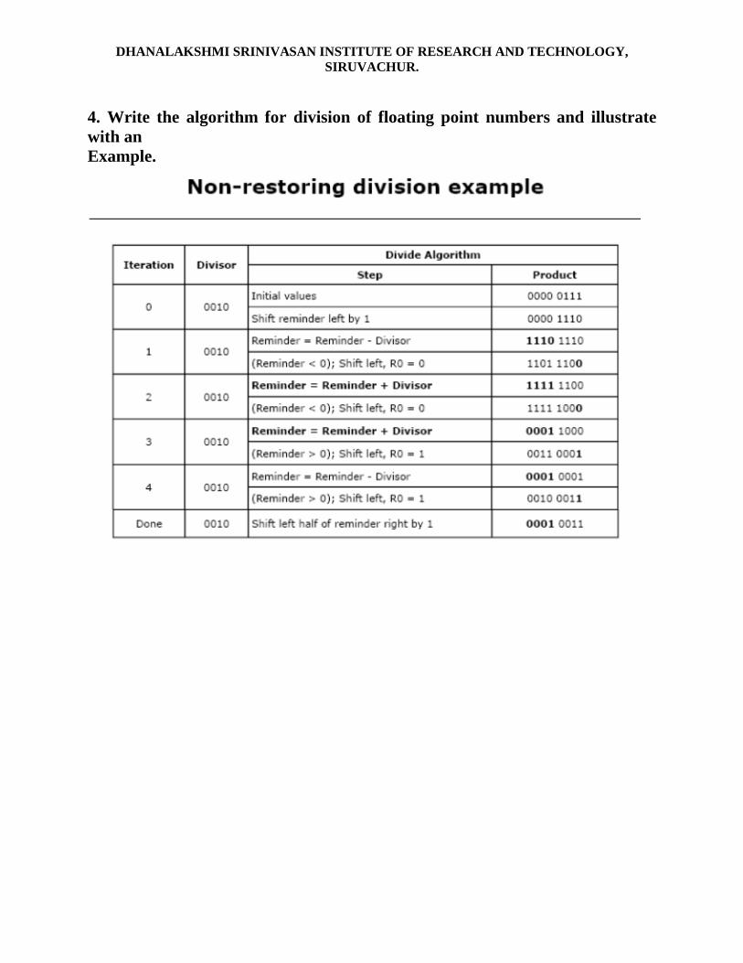
4. Write the algorithm for division of floating point numbers and illustrate with anExample.

DHANALAKSHMI SRINIVASAN INSTITUTE OF RESEARCH AND TECHNOLOGY,SIRUVACHUR.

DHANALAKSHMI SRINIVASAN INSTITUTE OF RESEARCH AND TECHNOLOGY,SIRUVACHUR.
UNIT III
1. (a). Write short notes on Nano Programming.Nanoprogramming
– Use a 2-level control storage organization– Top level is a vertical format memory» Output of the top level memory drives the address register of the bottom(nano- level) memory– Nanomemory uses the horizontal format» Produces the actual control signaloutputs– The advantage to this approach is significant saving in control memory size (bits)– Disadvantage is more complexity and slower operation (doing 2 memoryaccesses fro each microinstruction)Nano programmed machine� Example: Supppose that a system is being designed with 200 control pointsand 2048 microinstructions– Assume that only 256 different combinations of control points are ever used– A single-level control memory would require 2048x200=409,600 storage bits� A nano programmed system would use» Microstore of size 2048x8=16k» Nanostore of size 256x200=51200» Total size = 67,584 storage bits� Nano programming has been used in many CISC microprocessorsApplications of Microprogramming� Microprogramming application: emulation– The use of a microprogram on one machine to execute programs originallywritten to run on another (different!) machine– By changing the microcode of a machine, you can make it execute softwarefrom another machine– Commonly used in the past to permit new machines to continue to run oldsoftware» VAX11-780 had 2 ―modes�(b). Describe the characteristics of super scalar processing.Today, a computer designer is usually faced with maintaining binary compatibility, i.e.,maintaining instruction set compatibility and a sequential execution model (which typically implies precise interrupts1). For high performance, however, superscalar processor

DHANALAKSHMI SRINIVASAN INSTITUTE OF RESEARCH AND TECHNOLOGY,SIRUVACHUR.
implementations deviate radically from sequential execution -- much has to be done in parallel. As a result, the program binary nowadays should viewed as a specification of what has to be done, not how it is done in reality. A modern superscalar microprocessor takes the sequential specification as embodied in the program binary and removes much of the nonessential sequentiality to turn the program into a parallel, higher-performance version, yet the processor retains the outward appearance of sequential execution.
1.3. Elements of High Performance ProcessingSimply stated, achieving higher performance means processing a given program in a smaller amount of time. Each individual instruction takes some time to fetch and execute; this time is the instruction’s latency. To reduce the time to execute a sequence of instructions (e.g. a program), one can: (i) reduce individual instruction latencies, or (ii) execute more instructions in parallel. Because superscalar processor implementations are distinguished by the latter (while adequate attention is also paid to the former), we willconcentrate on the latter method in this paper.Nevertheless, a significant challenge in superscalar design is to not increase instruction latencies due to increased hardware complexity brought about by the drive for enhanced parallelism. Parallel instruction processing requires: the determination of the dependence relationships between instructions, adequate hardware resources to execute multiple operations in parallel, strategies to determine when an operation is ready for execution, and techniques to pass values from one operation to another. When the effects of instructions are committed, and the visible state of the machine updated, the appearance of sequential execution must be maintained. More precisely, in hardware terms, this means a superscalarprocessor implements:i) Instruction fetch strategies that simultaneously fetch multiple instructions, often by predicting the outcomes of, and fetching beyond, conditional branch instructions,ii) Methods for determining true dependences involving register values, and mechanisms for communicating these values to where they are needed during execution,iii) Methods for initiating, or issuing, multiple instructions in parallel,iv) Resources for parallel execution of many instructions, including multiple pipelined functional units and memory hierarchies capable of simultaneously servicing multiple memory references,v) Methods for communicating data values through memory via load and store instructions, and memory interfaces that allow for the dynamic and often unpredictable performance behavior of memory hierarchies. These interfaces must be well-matched with the instruction execution strategies.

DHANALAKSHMI SRINIVASAN INSTITUTE OF RESEARCH AND TECHNOLOGY,SIRUVACHUR.
vi) Methods for committing the process state in correct order; these mechanisms maintain an outward appearance of sequential execution. Although we will discuss the above items separately, in reality they cannot be completelyseparated – nor should they be. In good superscalar designs they are often integrated in a cohesive, almost seamless, manner.
2. Discuss the various hazards that might arise in a pipeline. What are the remedies commonly adopted to overcome/minimize these hazards.The Pipeline DefinedPipeliningJohn Hayes provides a definition of a pipeline as it applies to a computer processor."A pipeline processor consists of a sequence of processing circuits, called segments or stages, through which a stream of operands can be passed."Partial processing of the operands takes place in each segment."... a fully processed result is obtained only after an operand set has passed through the entire pipeline."In everyday life, people do many tasks in stages. For instance, when we do the laundry, we place a load in the washing machine. When it is done, it is transferred to the dryer and another load is placed in the washing machine. When the first load is dry, we pull it out for folding or ironing, moving the second load to the dryer and start a third load in the washing machine. We proceed with folding or ironing of the first load while the second and third loads are being dried and washed, respectively. We may have never thought of it this way but we do laundry by pipeline processing.A Pipeline is a series of stages, where some work is done at each stage. The work is not finished until it has passed through all stages.Let us review Hayes' definition as it pertains to our laundry example. The washingmachine is one "sequence of processing circuits" or a stage. The second is the dryer. The third is the folding or ironing stage."A significant aspect of our civilization is the division of labor. Major engineeringachievements are based o n subdividing the total work into individual tasks which can be handled despite their inter-dependencies."Overlap and pipelining are essentially operation management techniques based on jobsub-divisions under a precedence constraint."

DHANALAKSHMI SRINIVASAN INSTITUTE OF RESEARCH AND TECHNOLOGY,SIRUVACHUR.
Types of Pipelines
Instructional pipeline:where different stages of an instruction fetch and execution are handled in a pipeline.Arithmetic pipeline:where different stages of an arithmetic operation are handled along the stages of a pipeline.The above definitions are correct but are based on a narrow perspective, consider only the central processor. There are other type of computing pipelines. Pipelines are used to compress and transfer video data. Another is the use of specialized hardware to perform graphics display tasks. Discussing graphics displays, Ware Myers wrote:"...the pipeline concept ... transforms a model of some object into representations that successively become more machine-dependent and finally results in an image upon a particular screen.This example of pipelining fits the definitions from Hayes and Chen but not the categories offered by Tabaz. These broader categories are beyond the scope of this paper and are mentioned only to alert the reader that different authors mean different things when referring to pipelining.DisadvanatgesThere are two disadvantages of pipeline architecture. The first is complexity. The second is the inability to continuously run the pipeline at full speed, i.e. the pipeline stalls.Let us examine why the pipeline cannot run at full speed. There are phenomena called pipeline hazards which disrupt the smooth execution of the pipeline. The resulting delays in the pipeline flow are called bubbles. These pipeline hazards include� structural hazards from hardware conflicts� data hazards arising from data dependencies� control hazards that come above from branch, jump, and other control flow changesThese issues can and are successfully dealt with. But detecting and avoidingthe hazards leads to a considerable increase in hardware complexity. The control paths controlling the gating between stages can contain more circuit levels than the data paths being controlled. In 1970, this complexity is one reason that led Foster to call pipelining"still-controversial" .1. Instruction fetch2. Instruction decode and register fetch

DHANALAKSHMI SRINIVASAN INSTITUTE OF RESEARCH AND TECHNOLOGY,SIRUVACHUR.
3. Execute4. Memory access5. Register write backHazards: When a programmer (or compiler) writes assembly code, they make theassumption that each instruction is executed before execution of the subsequent instruction is begun. This assumption is invalidated by pipelining. When this causes a program to behave incorrectly, the situation is known as a hazard. Various techniques for resolving hazards such as forwarding and stalling exist.Hazard (computer architecture)In computer architecture, a hazard is a potential problem that can happen in a pipelined processor. It refers to the possibility of erroneous computation when a CPU tries to simultaneously execute multiple instructions which exhibit data dependence. There are typically three types of hazards: data hazards, structural hazards, and branching hazards (control hazards).Instructions in a pipelined processor are performed in several stages, so that at any given time several instructions are being executed, and instructions may not be completed in the desired order.A hazard occurs when two or more of these simultaneous (possibly out of order) instructions conflict.� 1 Data hazardso 1.1 RAW - Read After Writeo 1.2 WAR - Write After Reado 1.3 WAW - Write After Write� 2 Structural hazards� 3 Branch (control) hazards� 4 Eliminating hazardso 4.1 Eliminating data hazardso 5.1 Eliminating branch hazardsData hazardsA major effect of pipelining is to change the relative timing of instructions by overlapping their execution.This introduces data and control hazards. Data hazards occur when the pipeline changes the order of read/write accesses to operands so that the order differs from the order seen by sequentially executing instructions on the unpipelined machine.Consider the pipelined execution of these instructions:1 2 3 4 5 6 7 8 9ADDR1, R2, R3 IF

DHANALAKSHMI SRINIVASAN INSTITUTE OF RESEARCH AND TECHNOLOGY,SIRUVACHUR.
IDEX MEMWBSUBR4, R5, R1 IFIDsubEX MEMWBANDR6, R1, R7 IF IDandEX MEMWBOR R8, R1, R9 IF IDor EX MEMWBXORR10,R1,R11 IF IDxorEX MEMWBAll the instructions after the ADD use the result of the ADD instruction (in R1). The ADD instruction writes the value of R1 in the WB stage (shown black), and the SUB instruction reads the value during ID stage (IDsub). This problem is called a data hazard. Unless precautions are taken to prevent it, the SUB instruction will read the wrong value and try to use it.The AND instruction is also affected by this data hazard. The write of R1 does not complete until the end of

DHANALAKSHMI SRINIVASAN INSTITUTE OF RESEARCH AND TECHNOLOGY,SIRUVACHUR.
cycle 5 (shown black). Thus, the AND instruction that reads the registers during cycle 4 (IDand) will receive the wrong result.The OR instruction can be made to operate without incurring a hazard by a simple implementation technique.The technique is to perform register file reads in the second half of the cycle, and writes in the first half.Because both WB for ADD and IDor for OR are performed in one cycle 5, the write to register file by ADDwill perform in the first half of the cycle, and the read of registers by OR will perform in the second half ofthe cycle.The XOR instruction operates properly, because its register read occur in cycle 6 after the register write byADD.The next page discusses forwarding, a technique to eliminate the stalls for the hazard involving the SUB and AND instructions.We will also classify the data hazards and consider the cases when stalls can not be eliminated. We will see what compiler can do to schedule the pipeline to avoid stalls.A hazard is created whenever there is a dependence between instructions, and they are close enough that the overlap caused by pipelining would change the order of access to an operand. Our example hazards have all been with register operands, but it is also possible to create a dependence by writing and reading the samememory location. In DLX pipeline, however, memory references are always kept in order, preventing this type of hazard from arising.All the data hazards discussed here involve registers within the CPU. By convention, the hazards are named by the ordering in the program that must be preserved by the pipeline.RAW (read after write)WAWWAR (write after read)(write after write)Consider two instructions i and j, with i occurring before j. The possible data hazards are:RAW (read after write) - j tries to read a source before i writes it, so j incorrectly gets the old value.This is the most common type of hazard and the kind that we use forwarding to overcome.WAW (write after write) - j tries to write an operand before it is written by i. The writes end up being

DHANALAKSHMI SRINIVASAN INSTITUTE OF RESEARCH AND TECHNOLOGY,SIRUVACHUR.
performed in the wrong order, leaving the value written by i rather than the value written by j in the destination.This hazard is present only in pipelines that write in more than one pipe stage or allow an instruction to proceed even when a previous instruction is stalled. The DLX integer pipeline writes a register only in WB and avoids this class of hazards.WAW hazards would be possible if we made the following two changes to the DLX pipeline:Here is a sequence of two instructions showing the execution in this revised pipeline, highlighting the pipe stage that writes the result:LW R1, 0(R2) IF ID EX MEM1 MEM2 WBADD R1, R2, R3 IF ID EX WBUnless this hazard is avoided, execution of this sequence on this revised pipeline will leave the result of the first write (the LW) in R1, rather than the result of the ADD.Allowing writes in different pipe stages introduces other problems, since two instructions can try to write during the same clock cycle. The DLX FP pipeline , which has both writes in different stages and differentpipeline lengths, will deal with both write conflicts and WAW hazards in detail.WAR (write after read) - j tries to write a destination before it is read by i , so i incorrectly gets the new value.This can not happen in our example pipeline because all reads are early (in ID) and all writes are late (in WB).This hazard occurs when there are some instructions that write results early in the instruction pipeline, and other instructions that read a source late in the pipeline.Because of the natural structure of a pipeline, which typically reads values before it writes results, such hazards are rare. Pipelines for complex instruction sets that support autoincrement addressing and requireoperands to be read late in the pipeline could create a WAR hazards. If we modified the DLX pipeline as in the above example and also read some operands late, such as the source value for a store instruction, a WAR hazard could occur. Here is the pipeline timing for such a potential hazard, highlighting the stage where the conflict occurs:SW R1, 0(R2) IF ID EX MEM1 MEM2 WBADD R2, R3, R4 IF ID EX WBIf the SW reads R2 during the second half of its MEM2 stage and the Add writes R2 during the first half of its WB stage, the SW will incorrectly read and store the value produced by the ADD.RAR (read after read) - this case is not a hazard :).Structural hazardsA structural hazard occurs when a part of the processor's hardware is needed by two or more instructions at the same time. A structural hazard might occur, for

DHANALAKSHMI SRINIVASAN INSTITUTE OF RESEARCH AND TECHNOLOGY,SIRUVACHUR.
instance, if a program were to execute a branch instruction followed by a computation instruction. Branch (control) hazardsBranching hazards (also known as control hazards) occur when the processor is told to branch - i.e., if a certain condition is true, then jump from one part of the instruction stream to another - not necessarily to the next instruction sequentially. In such a case, the processor cannot tell in advance whether it should process thenext instruction (when it may instead have to move to a distant instruction).This can result in the processor doing unwanted actions.A cache miss. A cache miss stalls all the instructions on pipeline both before and after the instruction causing the miss.A hazard in pipeline. Eliminating a hazard often requires that some instructions in the pipeline to be allowed to proceed while others are delayed. When the instruction is stalled, all the instructions issued later than thestalled instruction are also stalled. Instructions issued earlier than the stalled instruction must continue, since otherwise the hazard will never clear.A hazard causes pipeline bubbles to be inserted.The following table shows how the stalls are actually implemented. As a result, no new instructions are fetched during clock cycle 4, no instruction will finish during clock cycle 8.In case of structural hazards:Instr 1 2 3 4 5 6 7 8 9 10Instr i IFIDEX MEM WBInstr i+1 IF ID EX MEM WBInstr i+2 IF ID EX MEM WBStall bubble bubble bubble Bubble BubbleInstr i+3 IF ID EX MEM WBInstr i+4 IF ID EX MEM WBTo simplify the picture it is also commonly shown like this:Clock cycle numberInstr 1 2 3 4 5 6 7 8 9 10Instr i IF ID EX MEM WBInstr i+1 IF ID EX MEM WBInstr i+2 IF ID EX MEM WBInstr i+3 stall IF ID EX MEM WBInstr i+4 IF ID EX MEM WBIn case of data hazards:

DHANALAKSHMI SRINIVASAN INSTITUTE OF RESEARCH AND TECHNOLOGY,SIRUVACHUR.
Clock cycle numberInstr 1 2 3 4 5 6 7 8 9 10Instr i IF ID EX MEM WBInstr i+1 IF ID bubble EX MEM WBInstr i+2 IF bubble ID EX MEM WBInstr i+3 bubble IF ID EX MEM WBInstr i+4 IF ID EX MEM WBwhich appears the same with stalls:Clock cycle numberInstr 1 2 3 4 5 6 7 8 9 10Instr i IF ID EX MEM WBInstr i+1 IF ID stall EX MEM WBInstr i+2 IF stall ID EX MEM WBInstr i+3 stall IF ID EX MEM WBInstr i+4 IF ID EX MEM WB
UNIT IV
1.What do you mean by memory hierarchy ? Briefly discuss.
Memory is technically any form of electronic storage. Personal computer system have a hierarchical memory structure consisting of auxiliary memory (disks), main memory (DRAM) and cache memory (SRAM). A design objective of computer system architects is to have the memory hierarchy work as through it were entirely comprised of the fastest memory type in the system.
2. What is Cache memory? Cache memory: Active portion of program and data are stored in a fast small memory, the average memory access time can be reduced, thus reducing the execution time of the program. Such a fast small memory is referred to as cache memory. It is placed between the CPU and main memory as shown in figure.
3. What do you mean by interleaved memory? The memory is partitioned into a number of modules connected to a common memory address and data buses. A primary module is a memory array together with its own addressed data registers. Figure shows a memory unit with four modules.

DHANALAKSHMI SRINIVASAN INSTITUTE OF RESEARCH AND TECHNOLOGY,SIRUVACHUR.
4. How many memory chips of4128x8) are needed to provide memory capacity of 40 x 16. Memory capacity is 4096 x 16 Each chip is 128 8 No. of chips which is 128 x 8 of 4096 x 16 memory capacity
5. Explain about main memory. Ans. RAM is used as main memory or primary memory in the computer. This memory is mainly used by CPU so it is formed as primary memory RAM is also referred as the primary memory of computer. RAM is volatile memory because its contents erased up after the electrical power is switched off. ROM also come under category of primary memory. ROM is non volatile memory. Its contents will be retained even after electrical power is switched off. ROM is read only memory and RAM is read-write memory. Primary memory is the high speed memory. It can be accessed immediately and randomly.
UNIT V
1. Explain in detail about interrupt handling.INTERRUPT HANDLINGHandling Interrupts• Many situations where the processor should ignore interrupt requests–Interrupt-disable–Interrupt-enable•Typical scenario–Device raises interrupt request–Processor interrupts program being executed–Processor disables interrupts and acknowledges interrupt–Interrupt-service routine executed–Interrupts enabled and program execution resumedAn equivalent circuit for an open-drain bus used to implement a common interrupt-request line.Handling Multiple DevicesInterrupt Priority•During execution of interrupt-service routine–Disable interrupts from devices at the same level priority or lower–Continue to accept interrupt requests from higher priority devices–Privileged instructions executed in supervisor mode•Controlling device requests–Interrupt-enable

DHANALAKSHMI SRINIVASAN INSTITUTE OF RESEARCH AND TECHNOLOGY,SIRUVACHUR.
•KEN, DENPolled interrupts:Priority determined by the order in which processor polls the devices (polls their status registers)Vectored interrupts:Priority determined by the order in which processortells of INTA:If device has not requested service, passes the INTA signal to deviceto put its code on the address lines (order of connection in the chain)Daisy chaining next Device If needs service, does not pass the INTA, puts its code on the address lines PolledMultiple Interrupts•Priority in ProcessorStatus Word–Status Register --active program–Status Word --inactive program•Changed only by privileged instruction•Mode changes --automatic or by privileged•Interrupt enable/disable, by device, system-wideCommon Functions of Interrupts•Interrupt transfers control to the interrupt service routine, generally through the interrupt vector table, which contains the addresses of all the service routines.•Interrupt architecture must save the address of the interrupted instruction and the contents of the processor status register.Incoming interrupts are disabledwhile another interrupt is being processed to prevent a lost interrupt.•A software-generated interrupt may be caused either by an error or a user request (sometimes called a trap).•An operating system is interruptdriven.Hardware interrupts—from I/O devices, memory, processor, Software interrupts—Generatedby a program.
2. Explain in detail about standard I/O interface.From the discussions so far, the reader must have understood that the input/output system for a computer are accommodated in many layers, like memory devices.We have already discussed about cache memory and a special high speed bus to communicate with it, designated as cache bus. Main memory of the system is also interfaced with the processor with a dedicated memory bus so that delay in I/O operations, which is quite normal and happens frequently, does not retard the instruction that has to be carried out.The innermost layer of I/O devices is directly interfaced with the processor through its address, data and control bus (designated as I/O bus), and communicates in synchronous manner (synchronous parallel communication).

DHANALAKSHMI SRINIVASAN INSTITUTE OF RESEARCH AND TECHNOLOGY,SIRUVACHUR.
Note that although with processor these devices communicate in synchronous fashion, with the external world they communicate in asynchronous manner.Example of I/O devices of this layer may be 8255-based ports, timers/counters for real-time operations, USART for serial communication and other similar devices.Generic Model of IO ModuleCPU checks I/O module device status•I/O module returns status•If ready, CPU requests data transfer•I/O module gets data from device•I/O module transfers data to CPU
3. Describe the functions of SCSI with a neat diagram.SCSI Bus• Defined by ANSI – X3.131• Small Computer System Interface• 50, 68 or 80 pins• Max. transfer rate – 160 MB/s, 320 MB/s.
4. Discuss the DMA driven data transfer technique.Polling or interrupt driven I/O incurs considerable overhead–Multiple program instructions–Saving program state–Incrementing memory addresses–Keeping track of word count•Transfer large amounts of data at high speed without continuous intervention by the processor•Special control circuit required in the I/O device interface, called a DMA controllerDMA Controller•Part of the I/O device interface–DMA Channels•Performs functions that would normally be carried out by the processor–Provides memory address–Bus signals that control transfer–Keeps track of number of transfers•Under control of the processor

DHANALAKSHMI SRINIVASAN INSTITUTE OF RESEARCH AND TECHNOLOGY,SIRUVACHUR.
5. Describe Bus Arbitration.
· In a single bus architecture when more than one device requests the bus, a controller called bus arbiter decides who gets the bus, this is called the bus arbitration.· In computing, bus mastering is a feature supported by many bus architectures that enables a device connected to the bus to initiate transactions.· The procedure in bus communication that chooses between connected devices contending for control of the shared bus; the device currently in control of the bus is often termed the bus master. Devices may be allocated differing priority levels that will determine the choice of bus master in case of contention.· A device not currently bus master must request control of the bus before attempting to initiate a data transfer via the bus.· The normal protocol is that only one device may be bus master at any time and that all other devices act as slaves to this master.· Only a bus master may initiate a normal data transfer on the bus; slave devices respond to commands issued by the current bus master by supplying data requested or accepting data sent.� Centralized arbitration� Distributed arbitration· All devices have equal responsibility in carrying out the arbitration process.• Each device on the bus assigned an identification number.• Place their ID numbers on four open-collector lines.