ec1 2205 qb
DESCRIPTION
Electronics and communication EngineringTRANSCRIPT

DEPARTMENT OF ECE, ADHIPARASAKTHI COLLEGE OF ENGINEERING, KALAVAI.
147304 ELECTRONIC CIRCUITS 110
147304 ELECTRONIC CIRCUITS
AIM
The aim of this course is to familiarize the student with the analysis and design
of basic transistor Amplifier circuits and power supplies.
OBJECTIVE
On completion of this course the student will understand
The methods of biasing transistors
Design of simple amplifier circuits
Midband analysis of amplifier circuits using small - signal equivalent circuits
to determine gain input impedance and output impedance
Method of calculating cutoff frequencies and to determine bandwidth
Design of power amplifiers
Analysis and design of power supplies.
UNIT I TRANSISTOR BIAS STABILITY 9
BJT – Need for biasing – Stability factor - Fixed bias circuit, Load line and
quiescent point. Variation of quiescent point due to FEh variation within
manufacturers tolerance - Stability factors - Different types of biasing circuits -
Method of stabilizing the Q point - Advantage of Self bias (voltage divider bias)
over other types of biasing, Bias compensation – Diode, Thermister and
Sensistor compensations, Biasing the FET and MOSFET.
UNIT II MIDBAND ANALYSIS OF SMALL SIGNAL AMPLIFIERS 9
CE, CB and CC amplifiers - Method of drawing small-signal equivalent circuit - Midband analysis of various types of single stage amplifiers to obtain gain,
input impedance and output impedance - Miller’s theorem - Comparison of CB,
CE and CC amplifiers and their uses - Methods of increasing input impedance
using Darlington connection and bootstrapping - CS, CG and CD (FET)
amplifiers - Multistage amplifiers.
Basic emitter coupled differential amplifier circuit - Bisection theorem. Differential gain – CMRR - Use of constant current circuit to improve CMRR -
Derivation of transfer characteristic.
UNIT III FREQUENCY RESPONSE OF AMPLIFIERS 9
General shape of frequency response of amplifiers - Definition of cutoff
frequencies and bandwidth - Low frequency analysis of amplifiers to obtain
lower cutoff frequency Hybrid – equivalent circuit of BJTs - High frequency
analysis of BJT amplifiers to obtain upper cutoff frequency – Gain Bandwidth
Product - High frequency equivalent circuit of FETs - High frequency analysis of
FET amplifiers - Gain-bandwidth product of FETs - General expression for frequency response of multistage amplifiers - Calculation of overall upper and
lower cutoff frequencies of multistage amplifiers - Amplifier rise time and sag
and their relation to cutoff frequencies.

DEPARTMENT OF ECE, ADHIPARASAKTHI COLLEGE OF ENGINEERING, KALAVAI.
147304 ELECTRONIC CIRCUITS 111
UNIT IV LARGE SIGNAL AMPLIFIERS 9
Classification of amplifiers, Class A large signal amplifiers, second harmonic
distortion, higher order harmonic distortion, transformer-coupled class A audio
power amplifier – efficiency of Class A amplifiers. Class B amplifier – efficiency
- push-pull amplifier - distortion in amplifiers - complementary-symmetry (Class B) push-pull amplifier, Class C, Class D amplifier – Class S amplifier –
MOSFET power amplifier, Thermal stability and heat sink.
UNIT V RECTIFIERS AND POWER SUPPLIES 9
Classification of power supplies, Rectifiers - Half-wave, full-wave and bridge
rectifiers with resistive load. Analysis for dcV and ripple voltage with C, L, LC
and CLC filters. Voltage multipliers, Voltage regulators - Zener diode regulator,
principles of obtaining a regulated power supply, regulator with current
limiting, Over voltage protection, Switched mode power supply (SMPS), Power control using SCR.
TUTORIAL = 15 TOTAL : 60
TEXT BOOKS
1. Millman J and Halkias .C., Integrated Electronics, TMH, 2007.
2. S. Salivahanan, N. Suresh Kumar and A. Vallavaraj, Electronic Devices and
Circuits, 2nd Edition, TMH, 2007.
REFERENCES
1. Robert L. Boylestad and Louis Nashelsky, Electronic Devices and Circuit Theory, 9th Edition, Pearson Education / PHI, 2007.
2. David A. Bell, Electronic Devices & Circuits, 4th Ediion, PHI, 2007
3. Floyd, Electronic Devices, Sixth Edition, Pearson Education, 2002.
4. I.J. Nagrath, Electronic Devices and Circuits, PHI, 2007.
5. Anwar A. Khan and Kanchan K. Dey, A First Course on Electronics, PHI,
2006.
6. B.P. Singh and Rekha Singh, Electronic Devices and Integrated Circuits,
Pearson Education, 2006.
7. Rashid M, Microelectronics Circuits, Thomson Learning, 2007.

DEPARTMENT OF ECE, ADHIPARASAKTHI COLLEGE OF ENGINEERING, KALAVAI.
147304 ELECTRONIC CIRCUITS 112
Two Marks Q&A
UNIT – I TRANSISTOR BIASING
1. What are the transistor parameters that vary with the temperature? ,ICO,VBeo are the parameters varying with the temperature.
2. What is Bias? What is the need for biasing?
The proper flow of zero signal collector current and the maintenance of proper collector emitter voltage during the passage of signal is know as
transistor biasing.
When a transistor is biased properly, it works efficiently and produces no
distortion in the output signal and thus operating point can be maintained
stable.
3. What do you understand by DC & AC load line?
DC Load Line
It is the line on the output characteristics of a transistor circuit which
gives the values of Ic & Vce corresponding to zero signal (or) DC
Conditions. AC Load Line
This is the line on the output characteristics of a transistor circuit which
gives the values of Ic & Vce when signal is applied.
4. What is the meant by operating point Q? The zero signal values of Ic & Vce are known as operating point. It is
also called so because the variations of Ic and Vce take place about this
point, when the signal is applied.
5. What are the types of biasing? The different types of biasing are
(i) Fixed bias
(ii) Collector to Base bias (or) Feedback bias
(iii) Self bias (or) Voltage divider bias
6. What are all the factors that affect the stability of the operating point? The following are the factors that affect the stability of the operating
point,
a. Change of due to replacement of transistors.
b. Thermal variations
7. Define stability factor ‘S’?
The stability factor is defined as the rate of change of collector current Ic
with respect to the reverse saturation collector current Ico, keeping ‘Vbe’
and ‘ ’ constant.
8. What are the disadvantages of collector feedback bias? The disadvantages of feedback bias are
a. The collector current is high.
b. If AC signal voltage gain feedback into the resistor Re, it will
reduce the gain of the amplifier.

DEPARTMENT OF ECE, ADHIPARASAKTHI COLLEGE OF ENGINEERING, KALAVAI.
147304 ELECTRONIC CIRCUITS 113
9. Why voltage divider bias is commonly used in amplifier circuit?
The voltage divider bias has the following advantages a. the operating point will be in stable position.
b. The stability will be considerably improved.
c. Ic can be reduced to the collector leakage current ICO.
10.Define the stability factors S’ and S’’ ? The Stability factor S’ is defined as the rate of change of Ic with VBE
keeping ICO and constant.
The Stability factor S’’ is defined as the rate of change of Ic with
keeping VBE and ICO constant.
11.Give the stability factor S for the fixed bias circuit. The stability factor for the fixed bias circuit is,
12.Give the stability factor S for the Collector to base bias circuit. The stability factor for the Collector to base bias circuit is,
13.Give the stability factor S for the Voltage divider bias circuit.
The stability factor for the Voltage divider bias circuit is,
14. Why fixed bias circuit is not used in practice?
The stability of the fixed bias circuit is very less. Since the stability factor
S = 1+ , is a large quantity, therefore stability is less. So, it is not
used in amplifier circuits.
15. What are all the compensation techniques used for bias stability?
Along with the negative feedback, the following techniques are used for
the Q point stability. a. Diode compensation,
b. Thermistor compensation,
c. Sensistor compensation.
16.Why the input impedance of FET is more than that of a BJT?
The input impendence of FET is more than that of a BJT because the
input circuit of FET is reverse biased whereas the input circuit of BJT is
forward biased.
17.How FET is known as Voltage variable resistor?
In the region before pinch off, where VDS si small, the drain to source
resistance rd can be controlled by the bias voltage VGS. Therefore FET is
useful as voltage variable resistor (VVR) or Voltage dependent Resistor (VDR)

DEPARTMENT OF ECE, ADHIPARASAKTHI COLLEGE OF ENGINEERING, KALAVAI.
147304 ELECTRONIC CIRCUITS 114
18.List the advantages of Fixed bias method?
The advantages of fixed bias method are,
a. The stability of the operating point is greatly improved when compared with the other circuits.
b. Less cost and simple circuit.
19.How self-bias circuit is used as constant current source?
In the self bias circuit if Ic tends to increase because of ICO has increasing as a result of temperature, the current in RE increases. As a
consequences of the increase in voltage drop across RE that provides
negative feedback, the base current is decreased. Hence constant IC
value is maintained in the self bias circuit
20.What is Thermal runaway? The continuous increase in collector current due to poor biasing cause
the temperature at collector terminal to increase. If no stabilization is
done, the collector leakage current also increases. This further increases
the temperature. This action becomes cumulative and ultimately the
transistor burns out. The self destruction of an unstabilised transistor is known as thermal runaway.
21. What are the consideration factors that are used for the selection of an
operating point for an FET amplifier?
The consideration factors are, a. Output voltage swing,
b. Distortion,
c. Power dissipation,
d. Voltage gain,
e. Drift (or) Drain current.
22.Write the different types of FET biasing circuits.
The FET biasing circuits are classified as,
a. Gate bias,
b. Self bias
c. Voltage divider bias, d. Current source bias
e. Drain feedback bias
f. Zero bias.
23. What is meant by stabilization? The maintenance of the operating point fixed stable is known as
stabilization.

DEPARTMENT OF ECE, ADHIPARASAKTHI COLLEGE OF ENGINEERING, KALAVAI.
147304 ELECTRONIC CIRCUITS 115
UNIT – II MIDBAND ANALYSIS OF SMALL SIGNAL AMPLIFIERS
1. What is an amplifier?
An amplifier is a circuit, which can be used to increase the amplitude
of the input current or voltage at the output by means of energy drawn
from an external source.
2. Based on the transistor configuration how amplifiers are classified.
Based on transistor configuration, the amplifier are classified as
a. Common Emitter amplifier
b. Common Collector amplifier
c. Common Base amplifier
3. Draw a CE amplifier & its hybrid equivalent circuit.
4. Draw a CC amplifier & its hybrid equivalent circuit
5. Draw a CB amplifier & its hybrid equivalent circuit
6. Write the Hybrid parameters equation for transistor amplifier?
Vi = hi Ii + hrVo
Io = hf Ii + hoVo
7. Write the CE amplifier Current gain, Voltage gain, Input Impedance,
Output Impedance in terms of h-parameters. Current gain Ai = -hfe
Voltage gain Av = ( - hfeRL)/hie
Input Impedance Zi = hie
Output Impedance Zo = ( hfe+Rs)/(hoeRs + h)

DEPARTMENT OF ECE, ADHIPARASAKTHI COLLEGE OF ENGINEERING, KALAVAI.
147304 ELECTRONIC CIRCUITS 116
8. Write the current amplification factors of the three transistor amplifier
configurations. In a transistor amplifier with AC input signal, the ratio of change
in output current to the change in input current is known as the current
amplification factor.
9. Which amplifier is called as voltage follower? Why? The common collector transistor amplifier configuration is called
as voltage follower. Since it has unity voltage gain and because of its
very high input impedance. It doesn’t draw any input current from the
signal. So, the input signal is coupled to the output circuit without
making any distortion.
10.Why hybrid parameters are called so? Define them?
The dimensions of the hybrid parameters are not alike, that is they
are hybrid in nature so they are called hybrid parameters.
h11 = [ V1/I1] at V2=0; h11 = Input impedance with output port
short circuited. h12 = [ V1/V2] at I1=0; h12 = Reverse voltage gain with input
port open circuited.
h21 = [ I2/I1] at V2=0; h11 = Forward current gain with output
port short circuited.
h22 = [ I2/V2] at I1=0; h11 = output impedance with input port open circuited.
11.What are the salient features of hybrid parameters?
The salient features of hybrid parameters are,
a. h parameters are real numbers,
b. They are easy to measure. c. They are convenient to use in circuit analysis and design
d. Easily convertible from one configuration to other
e. Readily supplied by manufactures.
12. Write the input impedance, output impedance, voltage gain and current gain of the common emitter amplifier in terms of h parameters for the
fixed bias condition?
Current gain Ai = -hfe
Voltage gain Av = (hfeRC)/hie
Input Impedance Zi = hie Output Impedance Zo = RL ||RC
13. Define Miller effect in input capacitance?
For any inverting amplifier, the input capacitance will be increased
by a miller effect capacitance, sensitive to the gain of the amplifier and the inter electrode capacitance connected between the input and output
terminals of the active device.
CMi = (1-Av)Cf ; CMo=Cf
Cf = Inter electrode capacitance between input and output.

DEPARTMENT OF ECE, ADHIPARASAKTHI COLLEGE OF ENGINEERING, KALAVAI.
147304 ELECTRONIC CIRCUITS 117
14.What is a Darlington connection in the amplifiers?
A Darlington transistor connection provides a transistor having a
very large current gain, typically a few thousand. The main features of the Darlington connection is that the composite transistor acts as a
single unit with a current gain, that is the product of current gains of the
individual transistors.
D= 1 2
D = Darlington connection current gain
1 and 2 – Current gain of the transistors 1 & 2 in the Darlington
pair
15.Explain Miller’s theorem.
16.Draw the darlington connections using similar transistors
17.Draw the Darlington connection using complementary transistors.

DEPARTMENT OF ECE, ADHIPARASAKTHI COLLEGE OF ENGINEERING, KALAVAI.
147304 ELECTRONIC CIRCUITS 118
18.What does bootstrapping mean?
In Darlington transistor pair circuits, the input impedance is
reduced because of the biasing resistors in the circuit. To overcome this, decrease in the input resistance due to the biasing network, a small
capacitor and resistance R3 are added in the circuit. This improved the
input impedance of the darlington pair circuit.
C is added at the input side and R3 is connected between output
and input circuits. Reff = Effective input resistance.
Reff = R3/(1-Av)
Reff = Large value
Av= Voltage gain.
19.Why we go for differential amplifier? (or) What is the need of differential amplifier?
The need for differential amplifier arises in many physical
measurements, in medical electronics and in direct coupled amplifier
applications. In this amplifier, there will be no output voltage resulting
from thermal drifts or any other changes provided, changes in both halves of the circuits are equal.
20.Define Common Mode Rejection Ratio CMRR?
Common Mode Rejection Ratio is the figure of merit of a
differential amplifier and is given by,
21. What are the advantages of differential amplifier?
The advantages of differential amplifier are, a. Very stable
b. Low noise, low drift,
c. Variations in supply voltage, temperature etc., will not change
the gain of the amplitude.
d. Does not require any coupling capacitor. e. Frequency response is better.
22.What are the applications of a differential amplifier?
The applications of a differential amplifier are,
a. To measure many physical quantities,
b. Can be used as a direct coupled amplifier, c. Used in operational amplifier.
23.What does bootstrapping technique mean?
If one end of the resistor changes in voltage, the other end of the
resistor also moves through the same change in voltage. This technique is known as bootstrapping. It is used to increase the input impedance of
the darlington pair circuits.
DEPARTMENT OF ECE, ADHIPARASAKTHI COLLEGE OF ENGINEERING, KALAVAI.
147304 ELECTRONIC CIRCUITS 119
24.What are the limitations of h parameters?
The h parameters has the following limitations,
a. The accurate calculation of h parameters is difficult. b. A transistor behaves as a two port network for small signals
only, hence h parameters can be used to analyze only the
small signal amplifiers.
25.What is meant by unity gain frequency? The frequency at which the gain approaches unity is known as
unity gain frequency.
26. Define dynamic range of an amplifier?
Dynamic range of an amplifier is defined as the range over which
an active electronic device can produce a suitable output signal in response to an input signal.
27.What is a differential amplifier?
An amplifier that has two inputs and produces an output signal
that is a function of the difference between the two given inputs is called differential amplifier.
28.Why transformer coupling is not used in the initial stages of a multistage
amplifier?
The transformer-coupled amplifiers are not used in the initial
stages of a multistage amplifier because it produces unwanted noise. Once these signals are amplified, it cannot be eliminated by the other
stages hence the amplifier performance is deteriorates.
29.Write the need for constant current source for difference amplifier?
The necessary for constant current source for differential amplifier
to increase the common mode rejection ratio without changing the quiescent current and without lowering the forward current gain.
30. Why constant current source biasing is preferred for differential
amplifier?
The constant current source biasing is preferred for differential amplifier in order to increase the input resistance and to make the
common mode gain is zero.
31. What is Common mode voltage swing?
The common mode voltage swing is defined as the maximum peak input voltage which may be applied to either the input terminal
without causing abnormal operation or damage. Typically with power
supplies of +6v or –6V, the common mode voltage swing should not
exceed +2v
32.Why Re is replaced by a constant current bias in a differential amplifier?
The emitter supply VBE used for biasing purpose must become
larger as Re is increased in order to maintain the quiescent current at its
proper value. If the operating currents of the transistors are allowed to
decrease, this will lead to higher hie values and will tend to decrease
CMRR. To overcome this practical limitations RE is replaced by a constant current bias.
DEPARTMENT OF ECE, ADHIPARASAKTHI COLLEGE OF ENGINEERING, KALAVAI.
147304 ELECTRONIC CIRCUITS 120
33.What is the input impedance of differential amplifier with RE at its
emitter junction? The input impedance of a differential amplifier RL at its emitter
junction is RL= 2hie+(1+hfe)RE
34. What are the special features of a difference amplifier that used FETs?
The special features of difference amplifier using FET are, a. Very high input impedance.
b. The common mode rejection ability is increased which makes the
common gain almost zero.
35. State the various methods of improving CMRR?
The methods of improve CMRR are, a. Constant current bias method
b. Use of current mirror circuit
c. Use of active load
36.Write the two types linear differential amplifiers? The linear differential amplifiers are classified as,
a. Inverting amplifier.
b. Non Inverting amplifier
37.Write the gain equation of inverting amplifier? The gain equation of inverting amplifier is,
Avf = Vo/Vin = -(Rf/Ri)
Avf= Gain with feedback
Rf = Feedback path resistor
Ri = Input resistor.
38.Write the configuration of differential amplifier?
The differential amplifier has the following configurations,
a. Dual input, balanced output differential amplifier,
b. Dual input, Unbalanced output differential amplifier,
c. Single input, balanced output differential amplifier, d. Single input, unbalanced output differential amplifier,
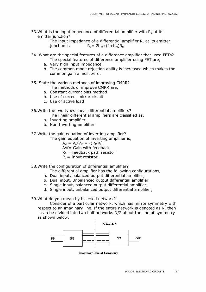
39.What do you mean by bisected network?
Consider of a particular network, which has mirror symmetry with
respect to an imaginary line. If the entire network is denoted as N, then it can be divided into two half networks N/2 about the line of symmetry
as shown below.
DEPARTMENT OF ECE, ADHIPARASAKTHI COLLEGE OF ENGINEERING, KALAVAI.
147304 ELECTRONIC CIRCUITS 121
The two half networks can be connected using any number of
wires but the wires are not crossing. This type of network is known as
bisected network.
40.Give the condition for analyzing the simplified Hybrid model of the
transistor amplifier?
The following condition should be satisfied for analyzing the
simplified hybrid model of transistor amplifier. hoe.RL<0.1
UNIT III – FREQUENCY RESPONSE OF AMPLIFIERS
1. Define the frequency response of Amplifier?
The frequency response of an amplifier can be defined as the
variation of output of quantity with respect to input signal frequency. In
otherwise it can be defined as a graph drawn between the input
frequency and the gain of an amplifier.
2. Define lower & upper cut off frequencies of an amplifier.
Lower cut-off frequency
The frequency (on lower side) at which the voltage gain of the
amplifier is exactly 70.0% of the maximum gain is known as lower cut off frequency.
Upper cut-off frequency
The frequency (on higher side) at which the voltage gain of the
amplifier is exactly 70.0% of the maximum gain is known as upper cut
off frequency.
3. Define bandwidth?
The range of frequencies occupied by the signal is known as its
bandwidth.
4. State the reason for fall in gain at low frequencies. The coupling capacitance has very high reactance at low
frequency. Therefore it will allow only a small part of signal from one
stage to next stage and in addition to that the bypass capacitor cannot
bypass or shunt the emitter resistor effectively. As a result of these
factors, the voltage gain rolls of at low frequency.
5. State the reason for fall in gain at higher frequencies?
At high frequency the reactance of coupling capacitor is very low.
Therefore it behaves like a short circuit. As a result of this the loading
effect of the next stage increase which reduces the voltage gain. Hence the voltage gain rolls off at high frequencies.
6. Why the electrolytic capacitor is not used for coupling?
Electrolytic capacitor is a polarized capacitor. So it cannot be used
for coupling and also in electrolytic capacitor, the dielectric is not an
insulating material but it conducting material which will change the capacitance effect.

DEPARTMENT OF ECE, ADHIPARASAKTHI COLLEGE OF ENGINEERING, KALAVAI.
147304 ELECTRONIC CIRCUITS 122
7. Write a note on effects of coupling capacitor.
a. The coupling capacitor Co transmits AC Signal. But blocks Dc. This prevents DC interferences between various stages and the shifting
of operating point.
b. It prevents the loading effect between adjacent stages.
8. Draw the low frequency simplified h-parameter model of an amplifier with a unbypassed emitter resistor.
9. Draw the hybrid- model of a transistor in the CE configuration (high
frequency model).
10.Why an NPN transistor has a better high frequency response than the
PNP transistor?
An NPN transistor has a better frequency response than the PNP
transistor because the mobility of electron is more and capacitive effect
is less.
11.Write an expression for the bandwidth of multistage amplifier.
The bandwidth of multistage amplifier is f2 – f1 = fo (21/n-1)
12.What is the significance of gain bandwidth product? It is very helpful in the preliminary design of a multistage
wideband amplifier. This can be used to setup a tentative circuit, which
is often used for this purpose.
13.Why is the gain bandwidth product a constant? It is defined as the magnitudes of the product of the mid band
gain which is a constant and the bandwidth, which is also a constant.
Hence the product of two constants should also be a constant.
14. Why N-channel FET’s have a better response than P-channel FET’s? N-channel FET have a better high frequency response than P-
channel FET due to the following reason.
a. Mobility of electrons is large in N-channel FET whereas the
mobility of holes is poor in P-channel FET.
b. The input noise is less in N-channel FET that that of the P-channel
FET. c. The trans conductance is larger in N-channel FET that that of P-
channel Fet.
DEPARTMENT OF ECE, ADHIPARASAKTHI COLLEGE OF ENGINEERING, KALAVAI.
147304 ELECTRONIC CIRCUITS 123
15.Define f T and f .
Unity gain frequency (f T) or frequency parameter. It is defined as the frequency at which the common emitter shirt
circuit current gain has dropped to unity and is denoted by the symbol
(fT)
Beta cut-off frequency (f )
It is defined as the high frequency at which -of a CE transistor
drops to 0.707 or 3dB from its lower frequencies
16.What is the need for having a high value of fT? Bandwidth of the amplifier is directly proportional to fT. hence tp
have larger bandwidth, the value of fT should be high.
17.What is a cascade amplifier?
The cascade configuration is an amplifier stage composed of a
direct coupled common emitter / common base combination. This offers the possibility of a very large bandwidth.
18.Write the relation between the bandwidth and rise time of an amplifiers?
BW=fH = 0.35/tr
19.Write the overall lower cut off frequency of multistage amplifier?
fL(n) = f L / ( (21/n-1))
Where f L(n) – lower 3 dB frequency of identical cascaded stages
n - Number of stages
20. Write the overall higher cut off frequency of multistage amplifier?
FH(n) = f H ( (21/n-1))
Where f H(n) – lower 3 dB frequency of identical cascaded stages n - Number of stages
21.Write the relation between the sag and lower cut-off frequency.
The tilt of sag in time t1 is given by
fL = pf / 100
p= Y of tilt f= input signal frequency
22.For an amplifier, midband gain is 100 and lower cut off frequency is
1kHz. Find the gain of an amplifier at the frequency of 20Hz.
A = (Amid)/( (1+(f1/f2)2))
A = (100)/( (1+(1000/20)2)) = 2
23.Write the relation between the sag and lower cutoff frequency? fH = 2.2 / (2 tr) = 0.35/tr
24. What is dominant network?
In high frequency analysis of an amplifier, the network having lower critical frequency is called dominant network.
25.What is the function of Miller input capacitance of an amplifier?
The Miller input capacitance of an amplifier is a function of Bypass
capacitor.

DEPARTMENT OF ECE, ADHIPARASAKTHI COLLEGE OF ENGINEERING, KALAVAI.
147304 ELECTRONIC CIRCUITS 124
26.What is the use of source bypass capacitor in CS amplifier?
Source bypass capacitor in CS amplifier is used for improving the
voltage gain.
27.Give two advantages of common source FET amplifier?
a. Good voltage gain
b. High input impedance.
28.What are the advantages of representation of gain in decibels?
a. In multistage amplifier, it permits to add individual gains of the
stages to calculate overall gain.
b. It allows us to denote, both very small as well as very large
quantities of linear scale by considerably small figures.
29.What is the coupling methods used for coupling in multistage amplifiers?
The coupling methods used are,
a. RC coupling
b. Transformer coupling
c. Direct coupling
UNIT IV - LARGE SIGNAL AMPLIFIERS
1. List out the classification of large signal amplifiers?
The large signal amplifiers are classified as follows. a. Based on the input
i. small signal amplifiers
ii. large signal amplifiers
b. Based on the output
I. Voltage amplifier
II. Power amplifier III. Current amplifier
c. Based on the transistor configuration
I. CE amplifier
II. CB amplifier
III. CC amplifier d. Based on the number of stages
I. Single stage amplifier
II. Multistage amplifier
e. Based on the Bandwidth
I. Untuned amplifier (wide band amplifier) II. Tuned amplifier (narrow band amplifier)
f. Based on the frequency response
I. AF (Audio frequency) amplifier
II. IF (Intermediate frequency) amplifier
III. RF (Radio Frequency) amplifier g. Based on the Biasing condition
I. Class A amplifier
II. Class B amplifier
III. Class C amplifier
IV. Class AB amplifier
V. Class D amplifier VI. Class S amplifier

DEPARTMENT OF ECE, ADHIPARASAKTHI COLLEGE OF ENGINEERING, KALAVAI.
147304 ELECTRONIC CIRCUITS 125
2. How do you bias the class A operation?
In class A mode, the output current flows through out the entire period of input cycle and the Q point is chosen at the midpoint of AC
load line and biased.
3. Which amplifier gives minimum distortion?
Class S amplifier gives minimum distortion.
4. Give the applications of class C power amplifier.
The applications of class C power amplifier are,
a. Used in radio and TV transmitters.
b. Used to amplify the high frequency signals.
c. Tuned amplifiers
5. Give the two draw backs of class C amplifier.
The drawbacks of class C amplifier are,
a. Distortion is high.
b. Figure of merit is low.
6. Define the following modes of operation (a) Class AB (b) Class C.
a. Class AB
In this mode of operation, the output current flows for more
than one half cycle but less than full cycle. b. Class C
In this mode, the level current flows for less than one half
cycled i.e., ¼ th of the input cycle.
7. Define Class B mode of operation and its advantages and disadvantages.
Class B mode of operation The Biasing signal and input signal flow through the circuit for
half cycle i.e., 180o.
Advantages
a. Efficiency is increased from 25% to 78.5%
b. Due to push pull configuration all even harmonics are reduced. So harmonic distortions are reduced.
c. Due to centre-tapped transformer at input and output, the core
saturation loss is reduced.
Disadvantages
a. Transistor is biased above the cut off region b. Due to the centre-tapped transformer at both input and output,
the circuit becomes complex
8. What is Class D amplifier?
In order to increase the conversion efficiency, it would be desirable to make the device to operate as a switch. So that its voltage
drop remains almost at minimum value over the half cycle of output
current flow. Such a system is called class D amplifier.
DEPARTMENT OF ECE, ADHIPARASAKTHI COLLEGE OF ENGINEERING, KALAVAI.
147304 ELECTRONIC CIRCUITS 126
9. State the merits of using push pull configuration.
The merits of push pull configurations are,
a. Efficiency is high (78.5%) b. Figure of merit is high
c. Distortion is less.
d. Ripple present in the output due to power supply is multiplied.
10.What are the advantages of using complementary symmetry configuration?
The advantages of using complementary symmetry configuration are,
a. It does not use centre-tapped transformer either at input or
output.
b. It uses one PNP transistor and one NPN transistor hence it
provides proper impedance matching. Hence its voltage gain is unity.
11.Define conversion efficiency of a power stage.
The ratio of the AC output power delivered to the load to DC input
power applied is referred to as conversion efficiency. It is also called as collector circuit efficiency in case of transistor amplifier.
Signal power delivered to the load x 100
= DC Power supplied at input circuit
12.Write down the values of maximum possible power conversion efficiency
for class A direct coupled and transformer coupled.
For class A direct coupled = 25%
For class A transformer coupled = 50%
13. What is cross over distortion?
In class B mode both transistors are biased at cut off region
because the DC bias voltage is zero. So input signal should exceed the
barrier voltage to make the transistor conduct. Otherwise the transistor doesn’t conduct. So there is a time interval between positive and
negative alternations of the input signal when neither transistor is
conducting. The resulting distortion in the output signal is cross over
distortion.
14.How cross over distortion is eliminated?
To avoid cross over distortion, a light forward bias (0.3Vfor ge
0.6V for Si) voltage is applied to the emitter junction of both the
transistors. It causes transistor to conduct immediately when the input
signal is applied. So Q point is fixed above cut off.
15.What are the drawbacks of the transformer coupled amplifier?
The disadvantages of transformer-coupled amplifiers are,
a. Transformer are bulky
b. Loss is more c. Centre-tapped of transformer is difficult.
16. Why RC coupling is popular?
RC coupling is popular because it is simple, less expensive, less
distortion and it provides uniform bandwidth.
DEPARTMENT OF ECE, ADHIPARASAKTHI COLLEGE OF ENGINEERING, KALAVAI.
147304 ELECTRONIC CIRCUITS 127
17.List the advantages of transformer coupled amplifier.
The advantages of transformer coupled amplifier are, a. it is more efficient because the low DC resistance of the primary is
connected to the collector circuit.
b. It provides excellence impedance matching, thus voltage and
power gains are improved.
18.What is the use of transformer coupling in the output stage of multistage
amplifier?
The transformer coupling provides impedance matching between
input and output. As a result the power gain is improved.
19.State the reason for fall in gain at low frequencies in the RC coupled amplifier.
a. The coupling capacitance (input) has very reactance at low
frequency. Therefore it will allow only a small part signal from one
stage to next stage.
b. The bypass capacitor cannot bypass or shunt the emitter resistor effectively.
As a result of these factors, the voltage gain rolls off at low
frequency.
20.State the reason for fall in gain at high frequencies. At high frequency, the reactance of coupling capacitor (output) is
very low. Therefore it provides like a short circuit. As a result of this, the
loading effect of the next stage increase which reduces the voltage gain.
Hence the voltage gain falls off at high frequencies.
21.What is amplitude or non linear distortion? In case of large signal amplifier, the input signals are large in
amplitude. So the operation extends to non linear region of its transfers
characteristics. Of the signal excursion enters the non-linear region then
distortion occurs in the output. Such a distortion is called non-linear
distortion.
22.Define figure of merit.
Figure of merit is defined as the ratio of maximum collector
current dissipation power to the maximum AC power developed across
the load.
23.Where S amplifiers are used?
The class S power amplifier can be used to amplify either the
constant amplitude or varying amplitude signal such as FM or AM signal.
24. Define inter modulation distortion?
Inter modulation distortion is a type of non-linear distortion.
Which generate frequency components not harmonically related to the
signal frequencies. It occurs when the input signal contains more than
the one frequency.

DEPARTMENT OF ECE, ADHIPARASAKTHI COLLEGE OF ENGINEERING, KALAVAI.
147304 ELECTRONIC CIRCUITS 128
25.What is the use of heat sink?
The heat sink is used to observe the heat produce in the transistor
junctions while its operation. Usually power amplifiers are provided with heat sinks. The heat sink is a large, black metallic heat-conducting
device placed in close contact with the transistor.
26.What is the maximum power dissipation hyperbola?
Maximum power dissipation hyperbola represents focus of all the points at which the collector dissipation is exactly Pc Max . The Q point
must lie on or below the hyperbola for safe operation.
27. Define thermal resistance.
The resistance offered by the bipolar junction transistor to the
flow of heat is called thermal resistance. The thermal resistance Q = QjA = QjC+QCS+QSA
o C/W
QjA = Total junction to ambient thermal resistance
QjC= Junction to case thermal resistance.
QCS= Case to heat sink resistance.
QSA=Heat sink to ambient resistance. 28.Write the maximum power handling of the class C power amplifier?
The maximum power in class C power amplifier is,
Pc max = 5/12 (T/To)(Vcc2/RL)
29.Write the advantages of heat sink? The advantages of heat sink are,
a. The temperature of the case gets lowered.
b. The power handling capacity of the transistors can approach the
rapid maximum value.
30.Write the derating factor expression of a power transistor? Pd(T1) = Pd(To) – (T1 - To)
Where Pd(To) = Rated power handling capacity at To
Pd(T1) = Power handling capacity at T1
The derating factor is expressed in the units of watts / degree of
temperature or milliwatts /degree of temperature.

DEPARTMENT OF ECE, ADHIPARASAKTHI COLLEGE OF ENGINEERING, KALAVAI.
147304 ELECTRONIC CIRCUITS 129
31.What is meant by thermal analogy of power transistors?
The heat dissipation problem is very much analogous to a simple
electric circuit and the ohm’s law. An electric current flows when there exists a potential difference while the heat flows when there exists a
temperature difference (T2-T1).
32.Write the Thermal-electric analogy parameters.
The following are the thermal-electric analogy parameters. Tj = Junction temperature
TC = Case temperature
TA = Ambient temperature
QjA = Total thermal resistance
QjC= Transistor thermal resistance.
QCS= Insulator thermal resistance. QSA=Heat sink thermal resistance.
UNIT V – RECTIFIERS AND POWER SUPPLIES
1. What is a power supply? Equipment, which converts the alternating waveform from the
power lines into an essentially direct voltage, is known as power supply.
2. What are all the subsystems in a power supply?
A power supply consists of following three subsystems. i. Rectifier.
ii. Filter
iii. Voltage regulator.
3. What is the function of rectifier?
Rectifier is capable of converting a sinusoidal input waveform. Its average value is zero, into a unidirectional waveform, with a non-zero
average component.
4. What is rectifier?
Any electrical device which offers a low resistance to the current in one direction but a high resistance to the current in the opposite
direction is called a rectifier. The rectifying device is usually a
semiconductor diode.
5. What is half – wave rectifier? The rectifier circuit which converts only the positive half cycle of
the AC input voltage input voltage into useful DC output voltage is
known as half-wave rectifier.
6. Write down the average DC voltage across the load in a half-wave rectifier circuit.
The average DC voltage is given by,
Vdc = IdcRL = Vm/{ (1+Rf/RL)
Rf= Diode forward resistance
RL= Load resistance Vm= Maximum amplitude or peak amplitude of the
sinusoidal AC input voltage

DEPARTMENT OF ECE, ADHIPARASAKTHI COLLEGE OF ENGINEERING, KALAVAI.
147304 ELECTRONIC CIRCUITS 130
7. Define ripple factor.
A measure of the purity of the DC output of a rectifier circuit is
called the ripple factor ‘r’ and is defined as, r = RMS value of AC components of wave Average value of wave
8. What is meant by peak inverse voltage?
The maximum reverse voltage capability of a diode is known as
peak inverse voltage.
9. What is meant by rectifier efficiency?
This is a figure used as a measure of merit to compare rectifiers.
The rectifier efficiency is defined as,
= DC power delivered to the load
AC input power from transformer secondary
10.What is full-wave rectifier?
A rectifier circuit, which converts both positive and negative half
cycle of the input AC voltage into useful DC voltage, is known as full
wave rectifier.
11.Write down the ripple factor and efficiency of the full-wave and half
wave rectifier circuits.
Full wave rectifier:
Ripple factor : 0.482
Efficiency : 81.2% Half wave rectifier:
Ripple factor : 1.21
Efficiency : 40.6%
12.What are all the drawbacks of a full wave rectifier?
The draw \backs of full wave rectifier are, i. centre tapped transformer is required.
ii. Diodes having twice the PIV rating are necessary in this
rectifier.
13.What are all the advantages of bridge rectifier circuit? The advantages of bridge rectifier circuit are,
i. The transformer utilization factor is high (0.812)
ii. It is suitable for large amount of DC power circuits.
iii. The peak inverse voltage across each diode is the peak Vm
only not 2Vm as in the case of two diode rectifier.
14.What is the average DC output voltage obtained in the bridge rectifier
circuit, and full wave rectifier circuit?
The DC output voltage of the bridge rectifier circuit is given by,
Vdc = 2Vm / - Idc(2Rf)
The DC output voltage of the full wave (two diode) rectifier circuit
is given by,
Vdc = 2Vm / { (1+Rf/RL)}
Rf = Diode forward resistance
RL = Load resistance

DEPARTMENT OF ECE, ADHIPARASAKTHI COLLEGE OF ENGINEERING, KALAVAI.
147304 ELECTRONIC CIRCUITS 131
15. What are all the disadvantages of half wave rectifier?
The disadvantages of half wave rectifier are,
i. Excess ripple (r=1.21) ii. Low rectification efficiency (40.6%)
iii. Low transformer utilization factor.
iv. DC saturation of transformer secondary winding.
16.Define transformer utilization factor of a rectifier circuit. The transformer utilization factor TUF is defined as,
TUF = DC power delivered to the load
AC rating of the transformer secondary
17.What is filter circuit?
Filter circuits are used to reduce the rectifier output ripple. Either
bypassing the AC output components around the load by a shunt capacitance or limiting this magnitude to a low value in the load by a
series inductance or a combination of these two for more efficient
circuits achieves this.
18. What are all the different types of filters? The different types of filters are,
i. Capacitor filter
ii. Series inductor filter
iii. LC filters
1. Capacitance input filter 2. Inductance input filter.
iv. RC filters.
19.How ripples are minimized in the capacitor filters?
In these types of filters a high value of capacitor is placed across
directly to the load resistor. This capacitor gets charged during the conduction period of the rectifier and when Vm decreases C gets
discharged through RL with a time constant CRL. The capacitor offers
only low impedance of 1/2 fc. this ripple component of current gets
bypassed through ‘C’
20.What are all the advantages and disadvantages of capacitor filters?
The advantages of capacitor filters are,
At high loads,
i. Small ripple voltage, ii. High output voltage.
The disadvantages are,
i. Poor regulation.
ii. High peak diode current.
21.Why we go for LC filter?
The simple shunt capacitor filter reduces ripple voltage but
increase the current through the diode. This large current may damage
the diode. The simple L filter reduces both peak value of output
current and output voltage. So we go for LC filters. This LC filters causes
enough removal of ripple and restriction on the diode current.

DEPARTMENT OF ECE, ADHIPARASAKTHI COLLEGE OF ENGINEERING, KALAVAI.
147304 ELECTRONIC CIRCUITS 132
22.Write the average DC voltage and ripple factor of the capacitor filter
rectifier circuits.
The average DC voltage of the capacitor filter rectifier circuit is given by,
Vdc = V m-Idc/4fC
Where f = Power line frequency.
C= Filter capacitor.
The ripple factor of the capacitor filter rectifier circuit is given by, r = Idc/(4 3 fCRL)
23.Write the average DC voltage and ripple factor of the inductor filter
circuit.
The average DC voltage of the inductor filter circuit of given by, Vdc = (2Vm/ ) - IdcR
The ripple factor of the inductor filter circuit is given by,
r = RL/(16000 L)
24.What are all the merits and demerits of CLC filter?
The merits of CLC filter are,
i. Higher Dc voltage approximating Vm
ii. Smaller ripple factor.
The demerits of CLC filter are, i. Poor voltage regulation.
ii. Higher peak inverse voltage.
iii. High peak diode current.
25.What is voltage multiplier circuit? Voltage multiplier circuits have the capable of delivering a DC
voltage two or more times the peak value Vm of the applied AC voltage.
26.Name the commonly used voltage multiplier circuits
The commonly used voltage multiplier circuits are,
i. Voltage doublers ii. Voltage quadruples
iii. Voltage tripler
27.What does voltage regulator mean?
An electron, which keeps the output voltage constant irrespective of the variation in load current, line voltage and temperature is known
as electronic voltage regulator.
28.Which characteristic of the zener diode is useful for voltage regulation?
The reverse bias characteristic of zener diode is useful in voltage regulation. Since in the reverse biased condition, at the breakdown
voltage Vz, its reverse voltage remains constant for a large variation of
the reverse current.
DEPARTMENT OF ECE, ADHIPARASAKTHI COLLEGE OF ENGINEERING, KALAVAI.
147304 ELECTRONIC CIRCUITS 133
29.What is the meant by load regulation and line regulation of a powe
supply?
Load regulation The ability of the power supply to maintain the constant DC
output voltage for a wide variation in load current is called load
regulation.
Line regulation
The ability of the power supply to maintain the constant output voltage for the input supply fluctuations for a constant load is called line
regulation.
30. What is the main difference between LPS and SMPS?
In the case of LPS, it has the voltage control element (transistor
or zener diode), which dissipates the power equal to the voltage difference between an unregulated input voltage and a fixed output
voltage multiplied by the current flowing through it. In the case of
SMPS, the switching regulator acts as a variable power converter and
also non-dissipative type regulator.
31.What are all the advantages of SMPS?
The advantages of SMPS are,
i. Efficiency is high because of less heat dissipation.
ii. As the transformer size is very small. It will have a compact
unit. iii. Isolation from main supply without the need of large main
transformer.
iv. Very low ripple i.e., almost zero ripple factor, pure DC
output.
v. Better voltage regulation
vi. Higher TUF.
32.What are the disadvantages of series inductor filter?
The disadvantages of series inductor filter are,
i. Ripple increases with load resistance.
ii. It requires a high input voltage of transformer for a given DC output and this will increase the cost of the unit.
iii. Inductor is also expensive and bulky.
33.What are the advantages of shunt capacitor filter?
The advantages of shunt capacitor filter are, i. Low ripple voltage for small load currents.
ii. Output voltage is high for small load currents.
34.What are the disadvantages of shunt capacitor filter?
The disadvantages of shunt capacitor filter are, i. Voltage regulation is relatively poor.
ii. High ripple voltage for large load current.
iii. Peak diode current may damage the diodes.
35.Give the expression for ripple factor of L filter in FWR.
The ripple factor of L filter in FWR is expressed as, r = RL/(3 (2 L))

DEPARTMENT OF ECE, ADHIPARASAKTHI COLLEGE OF ENGINEERING, KALAVAI.
147304 ELECTRONIC CIRCUITS 134
36.Give the expression for ripple factor of FWR with shunt capacitor filter.
The ripple factor of FWR with shunt capacitor filter is expressed
as, r = 1/(2 3(fCRL))
37.What is bleeder resistor?
Bleeder resistor is a fixed resistor connected across the filter output terminals to provide a minimum load across the rectifier. The
main job of this resistor is to maintain the minimum current required for
optimum inductor operation.
38.What is SMPS?
SMPS stands for Switched Mode Power Supply. The SMPS does not use a transformer at the input, but operates directly from mains at a
supply frequency of 50Hz. The AC main is directly rectified and filtered
and the DC voltage so obtained is then used as an input to a switching
type DC-to-DC converter.
39.List the advantages of zener regulator.
The advantages of zener regulator are,
i. It is small and light weight.
ii. It provides voltage regulation over a wide range of current.
40.List the disadvantages of zener regulator.
The disadvantages of zener regulator are,
i. Circuit is expensive and complex.
ii. Radio frequency due to ON OFF switching.
41.What is the need of filter in power supply?
Filter can be used to remove unwanted AC ripple component
present in the pulsating DC.
42.Compare LMPS and SMPS.
S.No LMPS SMPS
1. The Control element is
operated in active region The control element is
operated in cut off or saturation region.
2. It needs bulky components like transformer.
It does not require transformer
3.
It is operated in very low frequency such as f=50Hz,
hence heavy filtering is
needed.
It is operated at high frequencies hence less
filtering is required.
43.Define ripple factor.
The output of the rectifier is pulsating DC type. The amount of AC
content in the output can be mathematically expressed by a factor called ripple factor.

DEPARTMENT OF ECE, ADHIPARASAKTHI COLLEGE OF ENGINEERING, KALAVAI.
147304 ELECTRONIC CIRCUITS 135
44. Write the expressions for the ripple factor of capacitor input and LC
filters.
The ripple factor of capacitor input filter is given by, r = 1/(4 3(fCRL))
The ripple factor of LC filter is given by,
r = 1/(6 2( 2LC))
45.What are the advantages, applications and limitations of voltage
multipliers?
Advantages
The important advantages of multipliers are the use of clamping
action to increase the peak-rectified voltage without increasing the rating of the input transformer. This is economical. The centre tap
transformer is also not required in the multiplier circuit.
Applications
The multipliers are used in TV receivers and cathodes ray tube
anode voltages. Limitations
If we add more and more stages of diode and capacitor are added
to chain the output voltage keeps on falling substantially.
46.What are the factors that define the safe operating area (SOA) of the transistor?
The factors which define the safe operating area (SOA) of the transistor
are,
i. Maximum collector current Ic max rating.
ii. Maximum collector to emitter voltage Vce max rating iii. Maximum power dissipation PD max rating
iv. Maximum junction temperature
v. Second breakdown
47.What is meant by second breakdown in a transistor?
The second breakdown is a phenomenon which results from the formation of hot spots within the transistor that causes unbalanced
sharing of the total load among the different parts of the transistor.
48.Write the applications of SCR.
The applications of SCR are, i. It can be used as a rectifier element like diode to convert
AC signals to DC signals.
ii. It is used to control the average power delivered to the load
by means of its switching property.
49.How SCR is used for DC power control?
By controlling the instant of turning ON the SCR, the average
power delivered to the load can be controlled.
The average value of the output voltage in SCR half wave rectifier
is given by,

DEPARTMENT OF ECE, ADHIPARASAKTHI COLLEGE OF ENGINEERING, KALAVAI.
147304 ELECTRONIC CIRCUITS 136
50.Define firing angle of SCR.
The angle of the input cycle at which the SCR is turned ON is
known as firing angle.
51. Draw the AC power control circuit using SCR.? The firing angle for both the SCRs is controlled by the gate
circuit in their respective half cycles.