easy test generation plas
TRANSCRIPT
Vol. 2 No. 1 J. of Comput. Sci. & Technol. 1987
Easy Test Generation PLAs Min Yinghua( f ~ )
(Chinese Academy of Railway Sciences)
Received December 13, 1985; revised August 15, 1986.
Abstract
Test Generation for large circuits may be extremely difficult. One of the approaches to alleviating this problem is to consider the difficulties during the design cycle. This paper proposes a design of Easy Test Generation Programmable Logic Arrays (ETG PLAs), for which test generation is basically not required, since a complete test set can be generated while the test is applied. This paper also presents procedure which makes a PLA an ETG PLA by following some design rules and providing reasonable
extra hardware.
1..Introduction
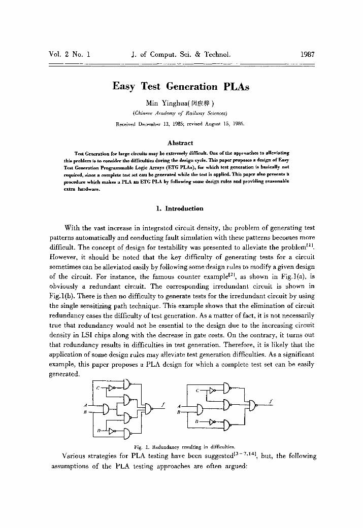
With the vast increase in integrated circuit density, the problem of generating test patterns automatically and conducting fault simulation with these patterns becomes more difficult. The concept of design for testability was presented to alleviate the problem tlJ. However, it should be noted that the key difficulty of generating tests for a circuit sometimes can be alleviated easily by following some design rules to modify a given design of the circuit. For instance, the famous counter example TM, as shown in Fig.l(a), is obviously a redundant circuit. The corresponding irredundant circuit is shown in Fig~l(b). There is then no difficulty to generate tests for the irredundant circuit by using the single sensitizing path technique. This example shows that the elimination of circuit redundancy eases the difficulty of test generation. As a matter of fact, it is not necessarily true that redundancy would not be essential to the design due to the increasing circuit density in LSI chips along with the decrease in gate costs. On the contrary, it turns out that redundancy results in difficulties in test generation. Therefore, it is likely that the application of some design rules may alleviate test generation difficulties. As a significant example, this paper proposes a PLA design for which a complete test set can be easily generated.
/
C
f
Fig. 1. Redundancy resulting in difficulties.
Various strategies for PLA testing have been suggested t3-7'141, but, the following
assumptions of the PLA testing approaches are often argued:

No. 1 Easy Test Generation PLAs 73
1.1. Single Faults
Many techniques are based on the single fault model, which is adequate for
maintenance test, when tests are so frequently applied that the first fault is detected
before the second fault occurs. The value of these techniques would be limited for
acceptance test, where many fault combinations may be present in a chip. Therefore, it is
likely that multiple faults should be taken into account because of the way in which PLAs are fabricated.
1.2. Irredundancy
Because of the difficulties inherent in test generation for redundant circuits, it is
desirable to eliminate such redundancy. But from PLA designer's point of view, redundancy inherently exists in PLAs.
This paper eliminates these restrictions, and defines Easy Test Generation (ETG)
PLAs, which makes it easy to generate tests for detecting single and multiple faults.
Complex test generation procedures are then no longer required for them. The fundamental idea was presented at FTCS-14 rt6J. The author pointed out in [16]
that extra inputs were also applicable for making a PLA an ETG PLA, and that the option
of adding extra inputs and/or outputs depended upon how many extra input and output
pins you had in your design environment. After that, S. Bozorgui-Nesbat et al. published tlTJ at ITC, in which a design of an ETG PLA was given by using extra input lines.
2. Easy Test Generation PLAs
Consider the modeled PLA structure with the bit lines xl, xl', "", xm, x,,' to the AND
array, the product lines wa, "", wn, the output lines zl, "", zp, and'the check bit outputs
q , "" ", cs. The crosspoint connecting the input line xi and the product line wj in the AND array is represented by (xi, w/), and similarly by (wj, zk) in the OR array. Extra/missing crosspoint defects in the AND or OR array are represented by AE, OE, AM, and OM
respectively. Let Z(wj) denote the output lines that are 1 when wj = 1, and {OM(wi, Z(wi))}
thus denotes the multiple fault composed of all missing crosspoint defects on wi in the OR
array. Z(wi) also denotes the output code of wi in the case of not being confused.
Lemma 1. A PLA can be modified, such that the outputs Z(w) o f the PLA are arranged into several inclusion sequences, which possess the following properties:
1. Z(w,1) _= .-- _ a w , , ) ;
2. for any i, 1 <~i ~ n, Z[w,) is in and only in a unique inclusion sequence; 3. f o r a n y j, 1 <~ j <~ p, {Z(w)lz~ = 1} is in an identical inclusion sequence. Proof Z(w) is a subset o fp dimensional Boolean vector space B p, and the inclusion
relation, __. , is a partial-ordering relation in B p. Therefore, it is always possible to arrange
all points in B l', as well as ~w), into disjoint inclusion sequences except the first and the
last points. The first and the last points of some inclusion sequences may be identical. In
this case, only one appearance of them is left, all the others are deleted, any L~wi) is then in
74 J. of Comput. Sci. & Technol. Vol. 2
and only in a unique inclusion sequence. Suppose there exists a zi and two inclusion
sequences, in one of which there is Z(wq) with zi = 1, and in the other there is Z(w,) with zg
= 1. In this case, w, is seperated into two product lines, w,' and w/', such that w,' = w," = w,, Z(w/) + Z(w/')= Z(w~), and Z(w/), is with zi = 1, while Z(w/')is with zi = 0 . After
this process, all output vectors with zi = 1 are then included in an identical inclusion sequense.
Suppose there are k inclusion sequences of the PLA as follows:
Z(w,,) __ Z(w,2)_=-.-_= Z(w,. 1)
Z(w 2) - . - (1)
Then, nl + n2 + " " + nk=n,~wi l )nZ(wi l )=O(1 <~ i , j <~ k,i # j), and for any wi, Z(wi) is included in a unique inclusion sequence.
Definition 1. {wit, wi2,'", wini}, 1 <. i <<. k, in (1) is called a relational group o f product lines, Z(wn) is called the output set o f the relational group. A PLA is called pseudo-nonconcurrent i f only one product line in any relational group is activated by each input pattern.
A pseudo-nonconcurrent PLA is not necessarily nonconcurrent [91, because more
than one product lines in different relational groups may be activated simultaneously.
Definition 2. Outputs o f two product lines, 2~wi) and Z(wj), i # j, are called exclusive, i f there is one bit being 0/1 and 1/0 respectively. A PLA is called exclusive, i f the outputs o f any pair o f product lines are exclusive.
Since output line sets of different relational groups are disjoint, the outputs of
product lines in different relational groups are exclusive. In order to let the outputs of
product lines in the same relational group be exclusive, it is necessary to add some check bits.
Definition 3. For the product line
W i = Xi 1Xi2
where x* = 0 or 1, x = "don't care", let
W ~ ~ �9 , , X i , 2(,i 2 " " " Xic i O " " O.
Then, a product line
w j = . ' . . . . : r .
is called belonging to the neighbourhood o f wi, i f w, and wj have opposite values, 0/1 or 1/0, at most in one bit. The neighbourhood o f w, is denoted by J(fvl). A PLA is called
separate, i f for any i, 1 ~ i <~ n,
E Z(wj)~Z(wi) (2) ,.:J(Y,,)
I f the condition (2) is not satisfied, the check bits are so selected that

No. 1 Easy Test Generation PLAs 75
E (Z(wj),C(wj)) ~(Z[w~), C(w~)). (3) w,~j(;,)
Suppose wi belongs to the following relational group:
~Oil , '" , Wia, Wi, Wi(a+ 2 ) , ' " , Win i"
Since L~wl)>1 Z(wi(a+ 2)) >" "'" >1 Z(wi,i),z~w,a+ 2)), ...,Z(wi,i) can be deleted in (2). That is to say, for the same relational group one only needs to consider those product lines whose
outputs have the same or more l's as or than wi. Definition 4. A PLA is called an Easy Test Generation PLA (ETG PLA), i f it is
pseudo-nonconcurrent and separate. The test set for an ETG PLA ean be simply generated as follows:
For each product line wi, suppose
* * . . . X * i X . . . g C ~ W i ~ XilXi2
~ W i ) = Z~Z* 2 " " Z ' p ,
~ W i ) = CI*C2*'"C*s ,
where x* represents x, or x,' (1/0), similar for z* and c*, x represents "don't care". Let
= * . . . x * O . . . O
T~)2 = XilXi2* *.--x*il...1 * , * . *
= % 0 . . . 0 (4)
= 0 . . . 0
and
, t ~'(~c i * * (Xici) 0 " " 0 ~ilXi2 ' ' '
(5) T = 0 Ti)
i = l
Then, T is the test set for the ETG PLA.
The test set T is capable of detecting the following faults:
1. Single ME faults. Suppose there exists an extra crosspoint defect on wi in the AND array, say
AE(x~ci+ 1, wi), then 7 ~ cannot activate wi. Let Z0 represent the output line set of the
relational group including wi. T~ cannot activate other product lines of the relational
group either. Even though 7~/~ possibly activates some product lines of the other
relational groups, the output lines are disjoint for different relational groups. Therefore,
there exists z~Z ~o, such that z ( 7 ~ ) = 0 for the faulty PLA, but 1 for the fault-free one.
2. Single OE faults. In the OR array of ETG PLAs, there are no crosspoints connecting product lines in a
76 J. of Comput. Sci. & Technol. Vol. 2
relational group and output lines in another relational group, since output lines in
different groups are completely different. Carefully folding during the chip design may
physically remove these crosspoints, it is thus not necessary to consider OE faufts at these
crosspoints. In order to detect OE(wi, zj), zjeZ (i), notice that for the fault-free PLA,
zj (T~)x) = 0, because there is no crosspoint connecting the output line zj and product lines
in other relational groups, while in the same group, only w~(T~)= 1, and there is no
device at (w~,zj). On the other hand, for the faulty PLA with OE(w~,zj),zj= 1. Detectable OE faults on check bit output lines result in an illegal check bit output
Z(~) l ) when T~)i is applied. Thus, T~)l and T~)2 detect all single OE faults on wi. 3. Single OM faults. Consider OM (w~,zj). For the fault-free PLA, zj (T~)~)= 1. But for the faulty PEA, it is
0. Because the crosspoint (wi, zj) is missing, there is no crosspoint connecting z~ and
product lines in other relational groups. Although zj may connect some product lines in
the same relational group, ~el'r(i) cannot activate these product lines because of the pseudo- nonconcurrency.
Similarly, OM faults on check bit output lines result in an illegal check bit output.
4. Single A M faults. Consider AM(x~*, w~). For the faulty PLA, T~r would activate wi, and we get
(Z( T#,),C( T#,)) >t (Z(w~), C(w,)). On the other hand, for the fault-free PLA,
(Z(T# , ) , = (Z(wj),C(wj)) TMr e Wj
Z C(w,)).
By (3) it is impossible that produces more output Vs than (Z(w,),C(w,)). AM( t, w,)is thus detected by T~,.
5. Multiple faults of the same mode in the same array. It is proved in the Theorem 5 in [14] that multiple faults of the same mode in the
same array can be detected by T whenever T detects one detectable single fault involved
in the multiple fault. Notice that multiple OE faults composed of undetectable OE faults
are still undetectable, similar conclusions hold for AM and OM faults. While for ETG
PLAs there is no undetectable AE faults, and then there is no basic multiple fault ciSl"
6. ,Single stuck-at faults and bridging faults between adjacent input lines or product lines.
This is obviously based on theorems in [15].
By (5) it is apparent that the size of the test set Tis less than or equal to {2n + the number cf connected crosspoints, in the AND array}, and thus less than (m+2)n .
3. The Construction of ETG PEAs
This section shows how to make a given PLA an ETG PLA. The construction
No. 1 Easy Test Generation PLAs 77
procedure consists of the following steps:
&ep 1. For the given PLA, arrange Z(w) into
Definition 5. The O-matrix o f the PLA is an
1, There is a device at (wi, zj), Oij= O, otherwise.
inclusion sequences.
n * p matrix, where
process continues until all neighbourhoods are considered.
The PLA becomes an ETG PLA by going through these steps.
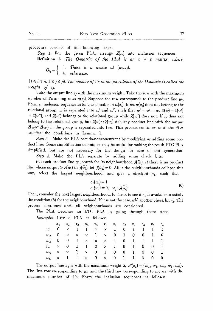
Example: Give a PLA as follows:
xl x2 x3 x4 x5 x6 zl z2 z3 z4 z5 z6 wl 0 x 1 1 x x 1 0 1 1 1 1
w2 0 x x x 1 x 0 1 0 0 1 0
w3 0 0 1 x x • 1 0 1 1 1 1
w4 x 0 1 1 0 x 1 0 1 0 0 1
ws x x 1 x 0 1 0 0 1 0 0 1
w6 x 1 1 x 0 x 0 1 1 0 0 0
The output line z3 is with the maximum weight
The first row corresponding to wl and the third row
maximum number of l's. Form the inclusion
5, W(z3)= {wl, w3, w4, w5, w6}. corresponding to Wz are with the
sequences as follows:
(1 ~< i ~< n, 1 ~ j<~ p). The number o f l ' s in the jth column o f the O-matrix is called the weight o f z~.
Take the output line zj with the maximum weight. Take the row with the maximum
number of l 's among rows w(zj). Suppose the row corresponds to the product line wi. Form an inclusion sequence as long as possible in w(zj). If wEu~(zj) does not belong to the
relational group, w is separated into w' and w", such that w" = w' = w, Z(w)= ~w' )
+ Z(w"), and Z(w') belongs to the relational group while Z(w") does not. If w does not
belong to the relational group, but Z ( w ) c ~ w i ) # 0, any product line with the output
Z(w)c~Z(wi) in the group is separated into two. This process continues until the pLA
satisfies the conditions in Lemma 1.
Step 2. Make the PLA pseud0-nonconcurrent by modifying or adding some pro-
duct lines. Some simplification techniques may be useful for making the result ETG PLA
simplified, but are not necessary for the design for ease of test generation.
Step 3. Make the PLA separate by adding some check bits.
For each product line wi, search for its neighbourhood J(zvi). If there is no product
line whose output >/Z(wi)in J(wi), let J(zTvi)= 0. After the neighbourhoods collapse this
way, select the largest neighbourhood, and give a checkbit q , such that
cl(wi) = 1 q(wj)=O, w;~J(w~) (6)
Then, consider the next largest neighbourhood, to check to see if cx is available to satisfy
the condition (6) for the neighbourhood. If it is not the case, add another check bit c2. The
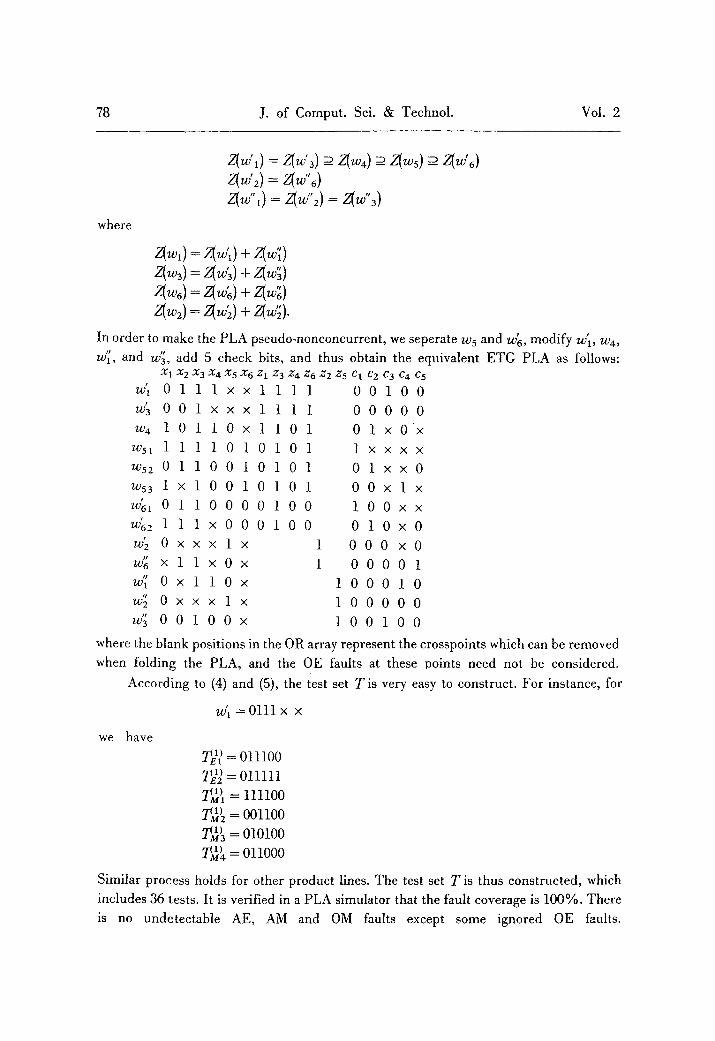
78 J. of Comput. Sci. & Technol. Vol. 2
where
z(~' i ) = z(w'~) _~ z (~ )~_ z (~ )__ z(~'6) z(~'~) = z(w"~) z(~",) = Z(w"~)= z(~"~)
z(wl) = Z(w,,)+ Z(w';)
z(~6) = Z(w'~)+ Z(w~) z ( ~ ) = z ~ ) + Zlw~).
In order to make the PLA pseudo-nonconcurrent, we seperate w5 and w~, modify w'l, w4,
w';, and w~, add 5 check bits, and thus obtain the equivalent ETG PLA as follows: ~1 X 2 X 3 X 4 X S X 6 Z 1 Z3 Z 4 Z 6 Z2 Z 5 C 1 C 2 C 3 C 4 C 5
w~ 0 1 1 l x x l 1 1 1 0 0 1 0 0
w~ 0 0 1 x x x 1 1 1 1 0 0 0 0 0
w4 1 0 1 1 0 x 1 1 0 1 0 l x 0 x
w51 1 1 1 1 0 1 0 1 0 1 1 x x x x
w52 0 1 1 0 0 1 0 1 0 1 0 l x x 0
ws3 l x 1 0 0 1 0 1 0 1 0 0 x l x
w~l 0 1 1 0 0 0 0 1 0 0 1 0 0 x x
w~z I 1 1 x 0 0 0 1 0 0 0 1 0 x 0
w~ O x x x l x 1 0 0 0 x O
w~ x 1 1 x O x 1 0 0 0 0 1
w~ 0 x 1 1 0 x 1 0 0 0 1 0
w~ O x x x l x 1 0 0 0 0 0
w~ 0 0 1 0 0 x 1 O 0 1 0 0
where the blank positions in the OR array represent the crosspoints which can be removed
when folding the PLA, and the OE faults at these points need not be considered.
According to (4) and (5), the test set Tis very easy to construct. For instance, for
we have
w'l = 0111 x x
Te~ = 011100
T~ = Olllll
~,~; = 1111oo
/ ~ = 001100
i~ = OlOlO0
~G =onooo
Similar process holds for other product lines. The test set Tis thus constructed, which
includes 36 tests. It is verified in a PLA simulator that the fault coverage is 100%. There
is no undetectable AE, AM and OM faults except some ignored OE faults.
No. 1 Easy Test Generation PLAs 79
4. Remarks
This paper defines an ETG PLA which is very easy to generate a complete test set.
The design for ease of test generation employs a procedure which either designs an ETG
PLA starting from a truth table or makes a PLA an ETG PLA by adding some product
lines and check bits. Extra inputs are also applicable for making a PLA an ETG PLA.
Some extra inputs may be useful for the reduction of extra product lines or output lines.
The option of adding extra inputs and/or outputs depends upon how many extra input
and output lines are available in your design environment. For instance, in the case of the
example in Section 3, adding 3 extra inputs results in the PLA, as denoted below, for
which the test set T given by (4) and (5) is complete and easy to generate.
~ ~ XI X 2 X 3 X 4 X 5 X 6 Z l Z2 Z3 Z 4 Z 5 Z6
wl 0 0 0 0 x 1 1 x x 1 0 1 1 1 1
w2 1 0 0 0 x x x 1 x 0 i 0 0 1 0
w3 0 1 1 0 0 1 x x x 1 0 1 1 1 1
w4 1 0 1 x 0 1 1 0 x 1 0 1 0 0 1
w5 1 1 0 x x 1 x O 1 O 0 1 0 0 1
w6 0 0 1 x 1 1 x O x O 1 1 0 0 0
technique is interesting in the ~llowing aspects: This
1. The assumptions of irredundancy and single fault model of PLAs under test are
omitted. The test set easily generated for ETG PLAs detects all single faults, the same
mode multiple faults in the same array, single stuck-at faults, and product line or input
line bridging faults.
2. Nonconcurrent PLAs defined in [9] possess many useful properties for testing,
but for which it is more difficult to detect missing faults than for ETG PLAs. In addition,
pseudo-nonconcurrent PLAs efficiently save silicon areas in comparison with
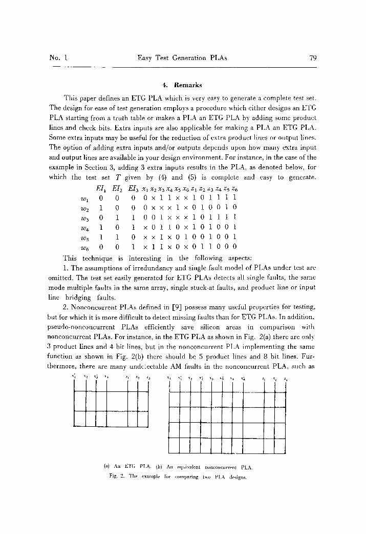
nonconcurrent PLAs. For instance, in the ETG PLA as shown in Fig. 2(a) there are only
3 product lines and 4 bit lines, but in the nonconcurrent PLA implementing the same
function as shown in Fig. 2(b) there should be 5 product lines and 8 bit lines. Fur-
thermore, there are many undc?ectable AM faults in the nonconcurrent PLA, such as
x" 1 x, x~ x., zl z z z~ xj x~ x, x~. xj x~ x.~ xlL z~ z~ z a
(a) An ETG PLA. (b) An equivalent nonconcurrent PLA.
Fig. 2. The example for comparing two PLA designs.

80 J. of Comput. Sci. & Technol. Vol. 2
AM(x~,,w2), AM(x~z, w3),--'. Although OM(w3,zl)is detectable, multiple fault {OM(w3,zl),AM(x'4, w2)} is unde-
tectable. The situation thus becomes more complicated for'generating a complete test set.
3. The test generation for an ETG PLA is so simple that the test inputs can be calculated at the time of test application and thus it makes the requirement of storing test
patterns unnecessary. The fault coverage is definitely 100%. 4. The design of ETG PLAs illustrates the difference between design for testability
and design for ease of test generation. As a matter of fact, there is an important issue of design for ease of test generation not only for PLAs but also for general combinational circuits. Some care should be taken during circuit design in order to ease test generation,
even though the circuit designed may not be minimized. Sometimes the technique of the design for ease of test generation is more efficient and with less extra hardware than that of the design for testability.
Acknowledgment
The author would like to thank Prof. E. J. McCluskey for his helpful discussions, and to thank Prof. Gan Junren and Liang Yewei for their comments and proofreading.
References
[ 1 ] T.W.William and K.P.Parker, Design for testability - - a Survey , IEEE Trans. on Comp. C-31:1(1982). [ 2 ] M.A.Breuer and A.D.Friedman, Diagnosis and Reliable Design of Digital Systems, Computer Science Press. MD,
1976. [ 3 ] D.L.Ostapko and S.J.Hong, Fault analysis and test generation for programmable logic arrays, [EEE Trans. on
Comp., C-28:9(1979). [ 4 ] J.E.Smith, Detection of faults in programmable logic arrays, IEEE Trans. on Comp., C-28:11(1979). [ 5] V.K.Agarwal, Multiple fault detection in programmable logic arrays, IEEE Trans. on Comp., C-29:6(1980). [ 6 ] F.B.Eichelberger and E.Lindbloom, A heuristic test pattern generation for programmable logic arrays, IBM.[. Res.
and Dev., 24:1,(1980). [ 7 ] P.Bose and J.A.Abrahafm, Test generation for programmable logic arrays, 19th Design Auto. Conf. Proc., las
Vegas, Nevada, 1982, 574--580, [ 8 ] J.Khakbaz and E.J.McCluskey, Concurrent error detection and testing for large PLAs, IEEE Trans. on Elec.
Devices; ED-29:4(1982). [ 9 ] S.L.Wang and A.Avizienis, The design of totally self-checking circuits usi~lg programmable logic arrays, Dig.
FTCS-9, Wisconsin, 1979. [10] H.Fujiwara and K.Kinoshita, A design of programmable logic arrays with universal tests, [EEE Trans. on Comp. C-
30:l(1981). [12] K.Son and D.K.Pradhan, Design of programmable logic arrays for testability, Dig. 1980 Test Conf., PA, 1980. [13] K.S.Ramanatha and N.N.Biswas, A design for testability of undetectable crosspoint faults in programmable logic
arrays, IEEE Trans. on Comp. C-32:6(1983). [14] Min Yinghua, Test generation for PLAs, J. o f Computers, 9:2(1986) (in Chinese). [15] Min Yinghua, A fauh model for PLAs, J. o f Computers, 9:1(1986) (in Chinese). [16] Min Yinghua, A PLA design for ease of test generation, the 14th Int'l conf. on FTC, FL, 1984 436--442. [17] S.Bozorgui-Nesbat and E.J.McCluskey, Lower overthead design for testability of PLAs, Int'l Test Conf., PA, 1984,
856-4365.