earth-abundant zinc-iv-nitride semiconductors phd thesis 2016.pdf · earth-abundant zinc-iv-nitride...
TRANSCRIPT

Earth-Abundant Zinc-IV-Nitride Semiconductors
Thesis by Naomi Cristina Coronel
In Partial Fulfillment of the Requirements for the Degree of
Doctor of Philosophy
California Institute of Technology Pasadena, California
2016
(Defended June 15, 2015)

ii
2016
Naomi Cristina Coronel
All Rights Reserved
iii
Acknowledgements
I would like to first thank Prof. Harry Atwater for providing an opportunity to research
such a challenging and interesting subject, and for his encouragement and optimism
throughout. I would also like to thank Prof. Julia Greer, Prof. Kaushik Bhattacharya,
Prof. Austin Minnich, and Prof. Brent Fultz for sharing their insights and perspectives as
members of my thesis and candidacy committees. I thank Carol Garland and Ali Ghaffari
for giving their time and energy to teach. I am grateful to have had the support of Lise
Lahourcade and Amanda Shing in our joint pursuit of zinc-IV-nitride materials, and I am
also thankful for the camaraderie of Yulia Tolstova, Samantha Wilson, Jeff Bosco, Greg
Kimball, and Davis Darvish in investigating earth-abundant semiconductors. Many
thanks to everyone in the Atwater group who contributed to this research in ways big and
small, especially to Tiffany Kimoto and Jennifer Blankenship for their continual support
and assistance. Finally, this work would not be possible without funding and support
from the DOE and Dow Chemical Company.
Naomi C. Coronel
June 2015
Pasadena, CA
iv
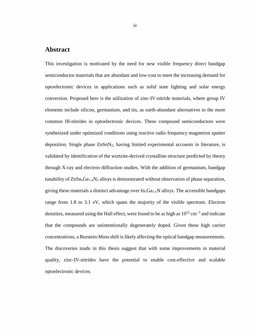
Abstract
This investigation is motivated by the need for new visible frequency direct bandgap
semiconductor materials that are abundant and low-cost to meet the increasing demand for
optoelectronic devices in applications such as solid state lighting and solar energy
conversion. Proposed here is the utilization of zinc-IV-nitride materials, where group IV
elements include silicon, germanium, and tin, as earth-abundant alternatives to the more
common III-nitrides in optoelectronic devices. These compound semiconductors were
synthesized under optimized conditions using reactive radio frequency magnetron sputter
deposition. Single phase ZnSnN2, having limited experimental accounts in literature, is
validated by identification of the wurtzite-derived crystalline structure predicted by theory
through X-ray and electron diffraction studies. With the addition of germanium, bandgap
tunability of ZnSnxGe1-xN2 alloys is demonstrated without observation of phase separation,
giving these materials a distinct advantage over InxGa1-xN alloys. The accessible bandgaps
range from 1.8 to 3.1 eV, which spans the majority of the visible spectrum. Electron
densities, measured using the Hall effect, were found to be as high as 1022 cm−3 and indicate
that the compounds are unintentionally degenerately doped. Given these high carrier
concentrations, a Burstein-Moss shift is likely affecting the optical bandgap measurements.
The discoveries made in this thesis suggest that with some improvements in material
quality, zinc-IV-nitrides have the potential to enable cost-effective and scalable
optoelectronic devices.

v
Contents
Acknowledgements iii
Abstract iv
List of Figures viii
List of Tables x
List of Publications xi
1 Introduction 1
1.1 Motivation for Studying Earth-Abundant Semiconductors . . . . . . . . 1
1.2 Zinc-IV-Nitride Literature Review . . . . . . . . . . . . . . . . . . . 2
1.2.1 Theory . . . . . . . . . . . . . . . . . . . . . . . . . . . 3
1.2.2 Synthesis . . . . . . . . . . . . . . . . . . . . . . . . . . 8
1.2.3 Characterization . . . . . . . . . . . . . . . . . . . . . . . 8
1.3 Scope of Thesis . . . . . . . . . . . . . . . . . . . . . . . . . . . 11
2 Synthesis of Stoichiometric ZnSnN2 12
2.1 Sputtering Chamber Capabilities . . . . . . . . . . . . . . . . . . . . 13
2.2 Achieving Stoichiometric Films . . . . . . . . . . . . . . . . . . . . 15
2.2.1 Sputtering From a Single Mixed Target . . . . . . . . . . . . 15
2.2.2 Sputtering From Two Elemental Targets . . . . . . . . . . . . 18

vi 2.3 Characterization of the Crystal Structure . . . . . . . . . . . . . . . . 23
2.3.1 Space Group . . . . . . . . . . . . . . . . . . . . . . . . . 23
2.3.2 Lattice Parameter Measurements . . . . . . . . . . . . . . . 25
2.4 Film Structure and Morphology . . . . . . . . . . . . . . . . . . . . 30
2.5 Conclusion . . . . . . . . . . . . . . . . . . . . . . . . . . . . . . 35
3 Tunable Bandgap ZnSnxGe1-xN2 Alloys 37
3.1 Linear Incorporation of Germanium to Form ZnSnxGe1-xN2 . . . . . . . 38
3.1.1 Measurements of Composition Variation . . . . . . . . . . . 39
3.1.2 X-ray Diffraction Studies of Phase Separation . . . . . . . . . 41
3.2 Optical Bandgap and Absorption Properties . . . . . . . . . . . . . . 44
3.3 Conclusion . . . . . . . . . . . . . . . . . . . . . . . . . . . . . . 48
4 Bulk Electronic Properties of ZnSnxGe1-xN2 52
4.1 Making Ohmic Contacts . . . . . . . . . . . . . . . . . . . . . . . 53
4.2 Majority Carrier Transport Properties . . . . . . . . . . . . . . . . . 55
4.2.1 Resistivity Measurements . . . . . . . . . . . . . . . . . . . 55
4.2.2 Carrier Density and Mobility . . . . . . . . . . . . . . . . . 57
4.3 Interactions between Optical and Electronic Properties . . . . . . . . . 60
4.4 Conclusion . . . . . . . . . . . . . . . . . . . . . . . . . . . . . . 64
5 Summary and Perspective 66
5.1 Summary of Thesis . . . . . . . . . . . . . . . . . . . . . . . . . . 66
5.2 Current and Future Work . . . . . . . . . . . . . . . . . . . . . . . 68
5.2.1 Material Synthesis . . . . . . . . . . . . . . . . . . . . . . 69

vii 5.2.2 Silicon-Containing Compounds . . . . . . . . . . . . . . . . 71
5.2.3 Point Defects . . . . . . . . . . . . . . . . . . . . . . . . 73
5.2.4 Improving Measurement Capabilities . . . . . . . . . . . . . 74
5.3 Benefit of Unintentional Degenerate Doping . . . . . . . . . . . . . . 76
5.4 Closing Remarks . . . . . . . . . . . . . . . . . . . . . . . . . . . 76
A Attempted Synthesis by Pulsed Laser Deposition 78
Bibliography 84
viii
List of Figures
1.1 Energy of wurtzite and zinc-blende structures. . . . . . . . . . . . . . . 3
1.2 Model of wurtzite-derived orthorhombic orderings, Pna21 and Pmc21 . . . 4
1.3 Calculated electronic band structure and density of states . . . . . . . . . 6
1.4 Theoretical bandgap vs. lattice constant of zinc-IV-nitrides . . . . . . . . 7
2.1 Schematic of reactive RF magnetron sputter deposition . . . . . . . . . . 14
2.2 Optimization of deposition form Zn0.75Sn0.25 target . . . . . . . . . . . . 16
2.3 Optimization of plasma power for co-sputtering . . . . . . . . . . . . . 18
2.4 Optimization of substrate temperature for co-sputtering . . . . . . . . . . 20
2.5 Optimization of gas pressure and composition for co-sputtering . . . . . . 22
2.6 Powder diffraction spectrum of ZnSnN2 . . . . . . . . . . . . . . . . . 24
2.7 Indexed SAED patterns of ZnSnN2 films . . . . . . . . . . . . . . . . . 28
2.8 XRD of ZnSnN2 films on c-sapphire and c-GaN substrates . . . . . . . . 31
2.9 XRD of ZnSnN2 films with varying tin plasma power . . . . . . . . . . . 32
2.10 XRD of ZnSnN2 films with varying gas pressure . . . . . . . . . . . . . 32
2.11 TEM bright field image of ZnSnN2 on c-sapphire substrate . . . . . . . . 33
2.12 SAED patterns of the interface between ZnSnN2 film and substrate . . . . 34
3.1 Composition of ZnSnxGe1-xN2 films . . . . . . . . . . . . . . . . . . . 40
3.2 Linear shift of XRD (002) peak with composition of ZnSnxGe1-xN2 . . . . 42
3.3 n(λ) and k(λ) of ZnSnN2 . . . . . . . . . . . . . . . . . . . . . . . . . 45
3.4 Optical bandgap estimation of ZnSnN2 . . . . . . . . . . . . . . . . . . 46

ix 3.5 Optical bandgap estimation of ZnGeN2 . . . . . . . . . . . . . . . . . . 48
3.6 Optical bandgap estimation of ZnSnxGe1-xN2 alloys . . . . . . . . . . . . 50
4.1 I-V curves of metal contacts on ZnSnxGe1-xN2 films . . . . . . . . . . . . 54
4.2 Resistivity of ZnSnxGe1-xN2 . . . . . . . . . . . . . . . . . . . . . . . 56
4.3 Schematic of Hall effect measurement geometry . . . . . . . . . . . . . 57
4.4 Carrier density and mobility of ZnSnxGe1-xN2 . . . . . . . . . . . . . . 59
4.5 Diagram of the Burstein-Moss effect . . . . . . . . . . . . . . . . . . . 61
4.6 Calculated Burstein-Moss shift for ZnSnN2 . . . . . . . . . . . . . . . . 63
5.1 High resolution TEM image of MBE-grown ZnSnN2 . . . . . . . . . . . 70
5.2 Shift of XRD (002) peak with composition of ZnSnxSi1-xN2 . . . . . . . . 71
5.3 Carrier density and mobility for ZnSnxSi1-xN2 . . . . . . . . . . . . . . 72
A.1 Schematic of pulsed laser deposition . . . . . . . . . . . . . . . . . . . 79
A.2 SEM images of PLD samples with varying substrate temperature . . . . . 80
A.3 XRD of PLD samples with high temperature nitridation . . . . . . . . . . 81
A.4 SEM image and composition of PLD sample deposited with N2 . . . . . . 83

x
List of Tables
1.1 Theoretical lattice parameters . . . . . . . . . . . . . . . . . . . . . . 5
1.2 Theoretical electronic bandgaps . . . . . . . . . . . . . . . . . . . . . 5
1.3 Experimental lattice parameter measurements . . . . . . . . . . . . . . 9
1.4 Experimental electronic bandgap measurements . . . . . . . . . . . . . 10
2.1 Measured ZnSnN2 lattice constants . . . . . . . . . . . . . . . . . . . 30

xi
List of Publications
Portions of this thesis have been drawn from the following publications:
P. Narang*, S. Chen*, N. C. Coronel*, S. Gul, J. Yano, L. Wang, N. S. Lewis, and
H. A. Atwater, “Band Gap Tunability in Zn(Sn,Ge)N2 Semiconductor Alloys,”
Advanced Materials, vol. 26, no. 8, pp. 1235–1241, 2014.
L. Lahourcade, N. C. Coronel, K. T. Delaney, S. K. Shukla, N. A. Spaldin, and H.
A. Atwater, “Structural and Optoelectronic Characterization of RF Sputtered
ZnSnN2,” Advanced Materials, vol. 25, no. 18, pp. 2562–2566, 2013.
N. C. Coronel, L. Lahourcade, K. T. Delaney, A. M. Shing, and H. A. Atwater,
“Earth-Abundant ZnSnxGe1−xN2 Alloys as Potential Photovoltaic Absorber
Materials,” Proceedings of the 38th IEEE Photovoltaic Specialists Conference
(PVSC), pp.003204-003207, 2012.
* denotes equal contribution
1
Chapter 1
Introduction
This thesis details the exploration of zinc-IV-nitrides, a new earth-abundant class of
semiconductor materials. Investigation of new materials is more important now than ever
for overcoming inherent material barriers to scalability, like cost or availability. Theory
predicts that zinc-IV-nitrides are well-suited for applications in optoelectronic devices,
although reports of experimental characterization are limited. The work presented here
strives to fill in some of the gaps in understanding of zinc-IV-nitride semiconductors.
1.1 Motivation for Studying Earth-Abundant Semiconductors
In today’s technological world, semiconductors play an increasing role in everyday life.
From computer chips to solar panels, semiconductors are in demand for more advanced
applications every day. As the prevalence of these materials increases, the question arises
as to whether or not current semiconductors are sustainable. This is an especially important
issue for industries like photovoltaics and light-emitting diodes (LEDs) because the scale
of their desired implementation is so large. This motivates the study of earth-abundant
semiconductors that are suitable for use in visible wavelength devices.
2 Many of the semiconducting materials that are widely used in current devices are
composed of elements that are not abundant enough in the earth’s crust to meet demand.
These include compounds containing gallium, selenium, cadmium, indium, and tellurium,
which precludes the majority of the materials used in high efficiency LEDs (GaN, InN)
and photovoltaics (GaAs, CdTe, CIGS). Cost is also a related value that can affect the
availability of certain materials. For example, the rapid adoption of ITO as a transparent
conducting film used in displays has increased the cost of indium, due in part to its relative
scarcity. Thus, switching over to earth-abundant materials will not only allow for large-
scale deployment of devices, but could also lower their cost.
There are also other environmental benefits to earth-abundant semiconductors.
Abundant elements are unlikely to be toxic to the environment as they are already present
in large quantities. This can reduce the need for expensive and cumbersome encapsulation
or disposal of devices, which is common for CdTe and GaAs photovoltaics.
One final requirement for semiconductors being used in optoelectronic devices is
that the material must have a high conversion efficiency. A device made with the cheapest,
most abundant elements will not be viable if the device is not efficient at its task. This is
the reason why it is important to study new earth-abundant semiconductors in-depth to
determine if they have potential for producing high efficiency devices.
1.2 Zinc-IV-Nitride Literature Review
This new system of materials is derived from III-nitrides, and is obtained by substitution
of group III elements with alternating group II and group IV elements. In this work, zinc
was chosen as the group II element and the group IV element is varied among silicon,

3 germanium, and tin. The close analogy of zinc-IV-nitrides to III-nitrides suggests the same
types of applications will be possible, with the added advantage of earth-abundance.
1.2.1 Theory
One of the main reasons that zinc-IV-nitrides are so interesting is that theoretical studies
suggest the optical properties are favorable for device applications. Density functional
theory (DFT) was the primary method of predicting these material properties, although the
selection of functional was varied in different reports.
The crystal structure of zinc-IV-nitride semiconductors is expected to be the same
as in the III-nitride system, hexagonal wurtzite with space group P63mc. In ZnSnN2, the
energetic difference between the wurtzite- and zinc-blende-derived orderings was found to
be small (Figure 1.1), suggesting that both phases could coexist under certain growth
Figure 1.1. Energy of wurtzite and zinc-blende structures as a function of unit
cell volume. Zinc-IV-nitrides are expected to form with the lower energy wurtzite
structure. [1]

4
conditions [3]. However, assuming that the zinc and group IV elements are ordered in the
lattice, an orthorhombic symmetry must be used to describe the unit cell instead. A model
of the wurtzite structure is depicted in Figure 1.2 alongside the orthorhombic space groups
that describe two different high-symmetry arrangements of the cations. Within the c-plane,
like-elements can be arranged in rows (Pmc21) or in a zig-zag pattern (Pna21). Most of the
theory work assumed the Pna21 space group for their calculations, as it is the most stable
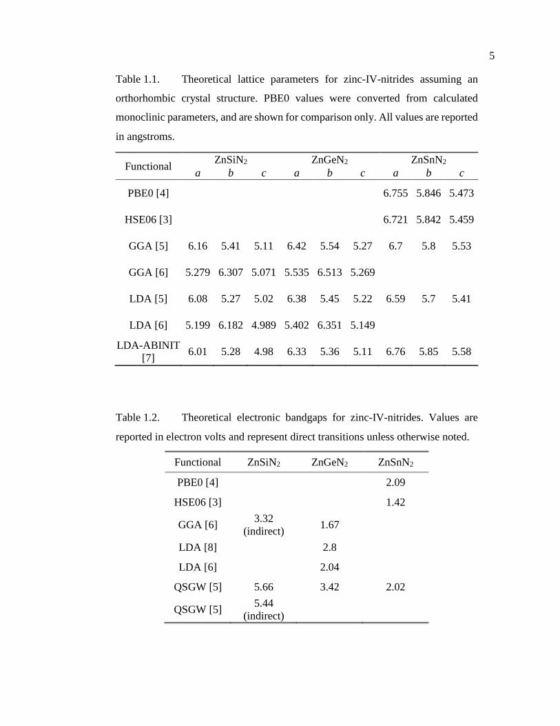
[3]. The resulting lattice parameters from the different calculations are shown in Table 1.1.
It should be noted that one study assumed a monoclinic crystal system in calculating their
Figure 1.2. Model of the hexagonal wurtzite structure and the two possible
ordering of cations in the c-plane. Pna21 is characterized by a zig-zag pattern of
like-atoms, and Pmc21 by rows of like-atoms.
5
Functional ZnSiN2 ZnGeN2 ZnSnN2
a b c a b c a b c
PBE0 [4] 6.755 5.846 5.473
HSE06 [3] 6.721 5.842 5.459
GGA [5] 6.16 5.41 5.11 6.42 5.54 5.27 6.7 5.8 5.53
GGA [6] 5.279 6.307 5.071 5.535 6.513 5.269
LDA [5] 6.08 5.27 5.02 6.38 5.45 5.22 6.59 5.7 5.41
LDA [6] 5.199 6.182 4.989 5.402 6.351 5.149
LDA-ABINIT [7] 6.01 5.28 4.98 6.33 5.36 5.11 6.76 5.85 5.58
Functional ZnSiN2 ZnGeN2 ZnSnN2
PBE0 [4] 2.09
HSE06 [3] 1.42
GGA [6] 3.32 (indirect) 1.67
LDA [8] 2.8
LDA [6] 2.04
QSGW [5] 5.66 3.42 2.02
QSGW [5] 5.44 (indirect)
Table 1.1. Theoretical lattice parameters for zinc-IV-nitrides assuming an
orthorhombic crystal structure. PBE0 values were converted from calculated
monoclinic parameters, and are shown for comparison only. All values are reported
in angstroms.
Table 1.2. Theoretical electronic bandgaps for zinc-IV-nitrides. Values are
reported in electron volts and represent direct transitions unless otherwise noted.
6 lattice parameters, and the correlating orthorhombic values are shown in Table 1.1 only for
comparison [4].
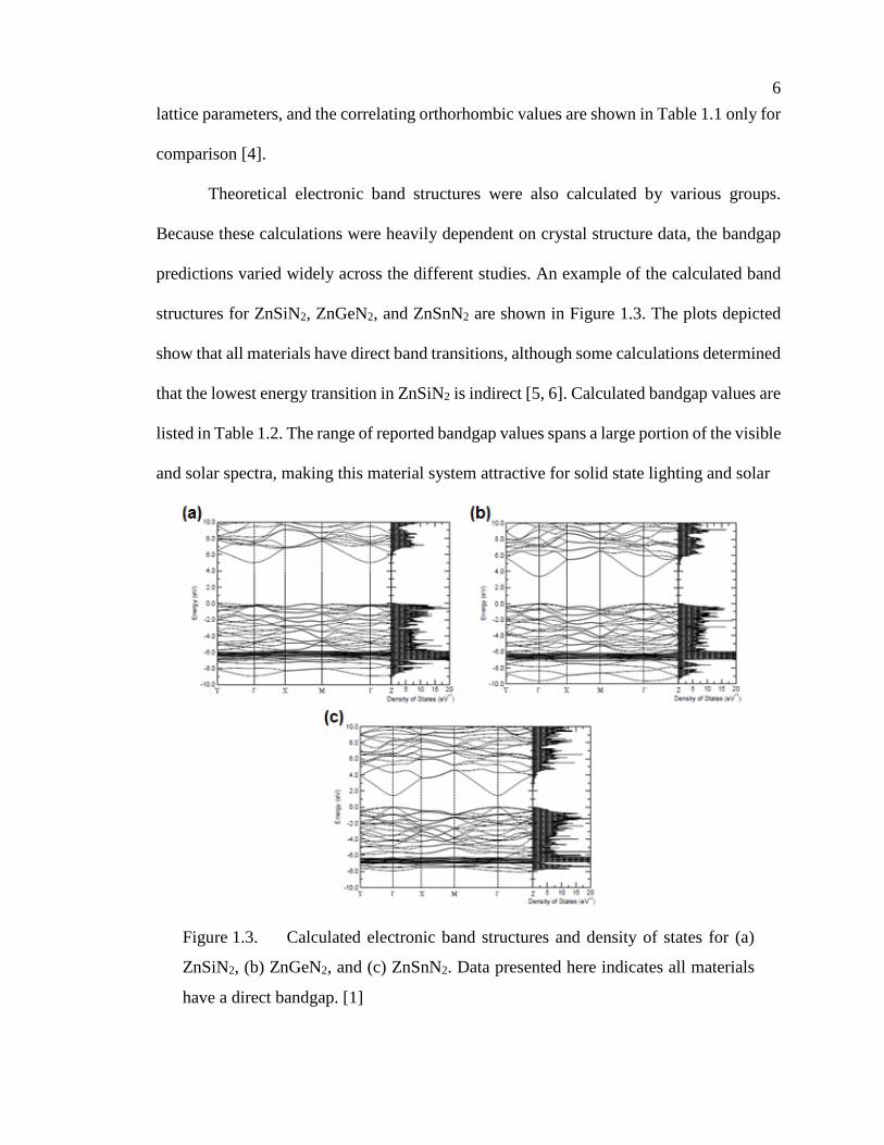
Theoretical electronic band structures were also calculated by various groups.
Because these calculations were heavily dependent on crystal structure data, the bandgap
predictions varied widely across the different studies. An example of the calculated band
structures for ZnSiN2, ZnGeN2, and ZnSnN2 are shown in Figure 1.3. The plots depicted
show that all materials have direct band transitions, although some calculations determined
that the lowest energy transition in ZnSiN2 is indirect [5, 6]. Calculated bandgap values are
listed in Table 1.2. The range of reported bandgap values spans a large portion of the visible
and solar spectra, making this material system attractive for solid state lighting and solar
Figure 1.3. Calculated electronic band structures and density of states for (a)
ZnSiN2, (b) ZnGeN2, and (c) ZnSnN2. Data presented here indicates all materials
have a direct bandgap. [1]

7 energy conversion applications. For comparison with the III-nitrides, a plot of theoretical
bandgap vs. lattice parameter is shown in Figure 1.4. The accessible bandgap range is
somewhat smaller in zinc-IV-nitrides, but the difference in lattice parameters is also
smaller, suggesting that alloying and formation of heterostructures will be more
straightforward.
Figure 1.4. Theoretical bandgap vs. lattice constant of zinc-IV-nitrides. Known
data points for the III-nitrides are included for comparison. The range of lattice
constants and bandgaps is smaller for zinc-IV-nitrides. [1]

8
1.2.2 Synthesis
There are many examples in the literature of both ZnSiN2 and ZnGeN2 synthesis. ZnSiN2
powder was synthesized using high-pressure annealing [2], and thin films have been grown
on sapphire, (100) silicon, or silicon carbide by metalorganic chemical vapor deposition
(MOCVD) [9-12]. More extensive efforts have been put into ZnGeN2 fabrication, leading
to powders made by reaction in a furnace [13-15], single crystal rods grown using a vapor-
liquid-solid (VLS) method [16], and thin films deposited on glass and silicon by radio
frequency (RF) sputter deposition and on sapphire and silicon carbide using MOCVD [9,
17-19]. Alloys of ZnSiN2 and ZnGeN2 have also been deposited by MOCVD [9, 12].
On the other hand, only very recently have reports surfaced of ZnSnN2 synthesis.
Polycrystalline crusts of ZnSnN2 have been formed by a VLS method [20] and thin films
were deposited by molecular beam epitaxy (MBE) [21].
1.2.3 Characterization
As with any new material, the first studies of zinc-IV-nitrides focused on characterizing
the crystal structure. Drawing from theoretical predictions, the unit cell was expected to be
a wurtzite-derived orthorhombic structure. However, various reports disagree about the
exact symmetry of these materials. A compilation of experimental lattice parameter
measurements are listed in Table 1.3 for the different crystal systems claimed. It should be
noted that the difference between the different results is very small, as the monoclinic and
orthorhombic crystals are simply slight distortions of the higher symmetry hexagonal

9
Crystal Structure a b c α β γ
ZnSi
N2
Orthorhombic [2] 5.2578(2) 6.3030(3) 5.0287(2)
Monoclinic [9] 3.09
Orthorhombic [10] 5.34 6.17 5.04
Orthorhombic [11] 5.05 6.18 5.35
ZnG
eN2
Monoclinic [13] 3.157(024) 3.157(024) 5.137(021) 119.5
Hexagonal [14] 3.193 5.187
Orthorhombic [22] 5.454 6.441 5.124
Hexagonal [17] 3.213 5.191
Orthorhombic [18] 5.50(20) 6.44(24) 5.14(25)
Hexagonal [19] 3.186(7) 5.174(12)
Monoclinic [23] 3.167 5.194 3.167 118.88
ZnSn
N2
Orthorhombic [20] 5.842(7) 6.753(6) 5.462(3)
Monoclinic [24] 3.395 3.4 5.534 89.885 90.033 120.036
Monoclinic [4] 3.375(1) 3.376(1) 5.532(3) 89.98 89.99 119.93
Monoclinic [4] 3.383(4) 3.379(3) 5.567(6) 89.97 89.96 119.95
one. Another important property was measurement of the electronic bandgaps of the
different compounds. Experimental estimations of the bandgaps using absorption and
photoluminescence are listed in Table 1.4. According to this data, the range of measured
ZnGeN2 bandgaps is quite large and there is no consensus on the value of the fundamental
bandgap energy.
Additionally, there are a few reports on investigation of the electronic properties of
zinc-IV-nitrides. One sample of ZnGeN2 was found to be electrically insulating [17], while
another was fairly conductive with a resistivity of 0.3-0.4 Ω∙cm [14]. The discrepancy is
Table 1.3. Experimental lattice parameter measurements for zinc-IV-nitrides.
a, b, and c values are in angstroms, and α, β, and γ values are in degrees.

10 probably due to the difference in synthesis methods for each result. For the conductive
material, electron concentrations and mobilities were also reported from Hall effect
measurements of 1018-1019 cm-3 and 0.5-5 cm2∙V-1∙s-1 [14]. Similar measurements of
ZnSnN2 films yielded electron concentrations of 1020-1021 cm-3 and mobilities of
10 cm2∙V-1∙s-1 [4]. Studies of phonon modes in ZnSiN2 and ZnGeN2 have also been
conducted using Raman and IR reflection spectroscopies [11, 15, 16, 25].
Reference ZnSiN2 ZnGeN2 ZnSnN2
[2] 3.64 (indirect)
[9] 4.46 3.2
[13] 3.40(1)
[14] 2.67
[15] 3.25
[17] 3.1
[26] 3.3
[27] 2.99(2)
[20] 1.7(1)
[4] 2.12, 2.38
Table 1.4. Experimental electronic bandgap measurements for zinc-IV-
nitrides. Values are reported in electron volts and represent direct transitions unless
otherwise noted.

11
1.3 Scope of Thesis
Based on the literature review of zinc-IV-nitride materials, there is certainly room for
additional characterization, as the intrinsic properties of the materials are not well
understood. For applications in optoelectronic devices, more information about the
absorption and electronic properties of ZnSnN2 and ZnGeN2 would also be valuable, since
these materials have bandgaps that are useful for interacting with visible light. A majority
of the prior research has focused on studying ZnGeN2 for use in optoelectronic devices
because of the popularity of its III-nitride analogue, GaN. In this thesis, an emphasis will
instead be placed on ZnSnN2 as it is the least studied material with the most promise for
visible light applications. Chapter 2 will describe the synthesis of ZnSnN2 by reactive
sputtering, for which synthesis had not yet been reported. Chapter 3 will explore tunable
bandgap alloys by incorporating germanium to form ZnSnxGe1-xN2. Optical bandgap
characterization of various compositions will also be included here. Chapter 4 will discuss
the challenges associated with carrier transport measurements, and tie the electronic
properties of the materials back to the optical properties. Finally, Chapter 5 will summarize
this thesis and identify topics for future work.

12
Chapter 2
Synthesis of Stoichiometric ZnSnN2
At the outset of this project there was no evidence in the literature proving synthesis of
ZnSnN2, let alone any experimental characterization of its properties. Because of its
predicted bandgap energy of 1.4 to 2 eV [3-5], this material is crucial for implementing the
zinc-IV-nitride system of materials into optoelectronic devices that interact with visible
light. It was therefore essential that the synthesis of ZnSnN2 be made a priority to begin
evaluating the potential of this material system as a whole.
This chapter describes the steps taken towards producing stoichiometric ZnSnN2
by reactive radio frequency (RF) magnetron sputter deposition, a physical vapor deposition
technique. Pulsed laser deposition (PLD) was another method used for initial synthesis
attempts, but the conditions did not allow for the formation of a homogeneous material (see
Appendix). The characterization of the structural properties of the sputter deposited
material is also described here, as it was important for demonstrating that the desired
material was created. Synthesis of single phase material was confirmed by studies of
composition using energy dispersive X-ray spectroscopy (EDXS), and X-ray diffraction
(XRD) revealed the wurtzite-derived Pna21 orthorhombic space group with unit cell
parameters measured by selected area electron diffraction (SAED). Because of the lack of
experimental research in the literature, verification of ZnSnN2 synthesis chiefly relied on
13 comparison with theoretical predictions of space group and lattice parameters, as well as
agreement with the patterns set by experimental work on ZnGeN2 and ZnSiN2. In addition,
films were generally oriented with the c-axis perpendicular to the surface of the substrate,
and were nearly epitaxial when grown on GaN, highlighting the smaller lattice mismatch
compared to sapphire.
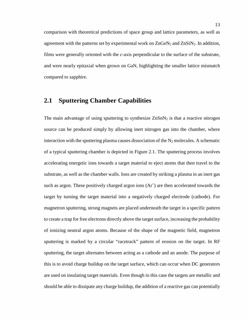
2.1 Sputtering Chamber Capabilities
The main advantage of using sputtering to synthesize ZnSnN2 is that a reactive nitrogen
source can be produced simply by allowing inert nitrogen gas into the chamber, where
interaction with the sputtering plasma causes dissociation of the N2 molecules. A schematic
of a typical sputtering chamber is depicted in Figure 2.1. The sputtering process involves
accelerating energetic ions towards a target material to eject atoms that then travel to the
substrate, as well as the chamber walls. Ions are created by striking a plasma in an inert gas
such as argon. These positively charged argon ions (Ar+) are then accelerated towards the
target by turning the target material into a negatively charged electrode (cathode). For
magnetron sputtering, strong magnets are placed underneath the target in a specific pattern
to create a trap for free electrons directly above the target surface, increasing the probability
of ionizing neutral argon atoms. Because of the shape of the magnetic field, magnetron
sputtering is marked by a circular “racetrack” pattern of erosion on the target. In RF
sputtering, the target alternates between acting as a cathode and an anode. The purpose of
this is to avoid charge buildup on the target surface, which can occur when DC generators
are used on insulating target materials. Even though in this case the targets are metallic and
should be able to dissipate any charge buildup, the addition of a reactive gas can potentially
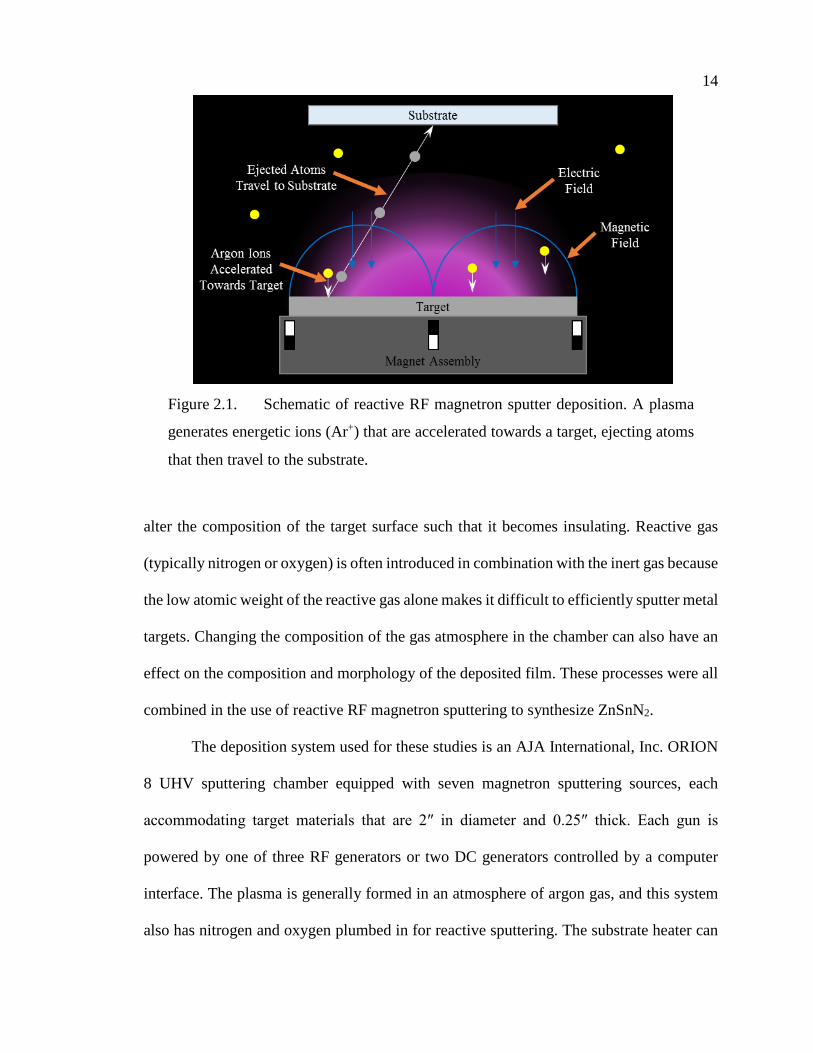
14
alter the composition of the target surface such that it becomes insulating. Reactive gas
(typically nitrogen or oxygen) is often introduced in combination with the inert gas because
the low atomic weight of the reactive gas alone makes it difficult to efficiently sputter metal
targets. Changing the composition of the gas atmosphere in the chamber can also have an
effect on the composition and morphology of the deposited film. These processes were all
combined in the use of reactive RF magnetron sputtering to synthesize ZnSnN2.
The deposition system used for these studies is an AJA International, Inc. ORION
8 UHV sputtering chamber equipped with seven magnetron sputtering sources, each
accommodating target materials that are 2″ in diameter and 0.25″ thick. Each gun is
powered by one of three RF generators or two DC generators controlled by a computer
interface. The plasma is generally formed in an atmosphere of argon gas, and this system
also has nitrogen and oxygen plumbed in for reactive sputtering. The substrate heater can
Figure 2.1. Schematic of reactive RF magnetron sputter deposition. A plasma
generates energetic ions (Ar+) that are accelerated towards a target, ejecting atoms
that then travel to the substrate.

15 reach up to 850 °C, and the base pressure in the chamber is on the order of 10-7 Torr, but
can be as low as 10-8 Torr after high-temperature baking.
2.2 Achieving Stoichiometric Films
In the initial exploration of ZnSnN2 sputter deposition, it was first important to ensure that
the desired stoichiometry could be achieved. Two different methods of deposition were
studied: sputtering from a single mixed ZnxSn1-x target and simultaneously sputtering from
elemental zinc and tin targets. The procedures for determining the optimal sputtering
conditions for each method are discussed here. Tunable deposition parameters included
substrate temperature, plasma power, gas pressure, and gas ratio. Film composition was
measured using EDXS with an Oxford X-Max SDD system attached to a ZEISS 1550 VP
field emission scanning electron microscope (SEM). The accelerating voltage in the SEM
was kept at 7-10 kV to constrain the excitation volume to the thickness of the film, which
is approximately 200-400 nm.
2.2.1 Sputtering From a Single Mixed Target
Early studies were carried out using a Zn0.50Sn0.50 pressed powder target acquired from ACI
Alloys, Inc. with 99.99% purity. This target only allowed for stoichiometric film growth
when the substrate temperature was below about 150 °C. At these low temperatures, the
surface mobility of the adsorbed atoms is low and the crystalline quality of the film suffers.
However at higher temperatures where the crystalline quality can be improved, the high
vapor pressure of zinc leads to a low sticking coefficient and results in zinc-poor films. The

16
zinc desorption at high temperatures can be compensated by a zinc-rich source material,
which prompted the use of a Zn0.75Sn0.25 pressed powder target for the remainder of the
single target studies.
In optimizing the deposition conditions using the Zn0.75Sn0.25 target (99.99%, ACI
Alloys, Inc.), it became evident that the first issue needing attention was excess oxygen
incorporation in the films during growth. It was important to limit the oxygen to avoid
characterization of zinc and tin oxides instead of the desired stoichiometric ZnSnN2. Figure
2.2a-b shows the composition of the films as a function of the plasma power and gas
Figure 2.2. Optimization of deposition parameters when sputtering from a
single Zn0.75Sn0.25 target. Composition measured by energy dispersive X-ray
spectroscopy from films with varying (a) plasma power, (b) gas pressure, and (c)
substrate temperature. Oxygen contamination is reduced in the films when plasma
power is high and gas pressure is low. Desired zinc/tin ratio is achieved when the
substrate temperature is near 250 °C. All other deposition parameters were held
constant as indicated in the top left corner of each panel.

17 pressure. A significant amount of oxygen is found in films deposited at low plasma powers
and high gas pressures. Both of these conditions decrease the deposition rate, which could
be as low as 1 nm ∙ min-1 for low powers and only a few nm ∙ h-1 for high pressures. In
these instances, the partial pressure of the deposited species is likely on the same order of
magnitude as the partial pressure of oxygen in the chamber and both are deposited with
comparable rates. Consequently, the combination of high plasma power and low gas
pressure gives the lowest oxygen concentration in the resulting films, most likely
correlating with an increased deposition rate and decreased relative partial pressure of
oxygen. Figure 2.2a-b also shows that when varying the plasma power and gas pressure,
there is no significant change in the ratio of zinc to tin, suggesting that the sputtering
efficiency of zinc and tin remains proportional under the tested conditions. Additionally,
the nitrogen composition appears to be inversely related to the amount of oxygen present
in the films such that the oxygen is likely being substituted onto nitrogen sites in the lattice
rather than being incorporated interstitially.
To control the zinc/tin ratio, the deposition temperature was varied using 164 W
plasma power and a gas pressure of 3 mTorr, which is the best power/pressure combination
identified to form a stable plasma and reduce the oxygen as much as possible. As illustrated
in Figure 2.2c, the films are highly zinc-rich below 200 °C, at which point a drastic drop
in zinc concentration occurs that correlates with the increase in tin and nitrogen atomic
percentages. However, the growth window for avoiding excessive zinc desorption is rather
small, as above 300 °C the layers become tin-rich. Therefore, the layer stoichiometry is
strongly sensitive to the temperature when sputtering from a single mixed target, allowing
for a small growth window of about 250 ± 25 °C. Under these conditions, material with the

18 desired stoichiometry for ZnSnN2 could be deposited reliably, but there is little room for
variation of the film properties.
2.2.2 Sputtering From Two Elemental Targets
Co-sputtering is a more desirable growth method because it has the advantage of
being able to more accurately control the atomic fluxes for each individual metal. In the
case of ZnSnN2, the single mixed targets also limited the temperature range for
stoichiometric growth. Removing the restriction of a fixed metal ratio could expand this
temperature range, which would be useful for altering the film morphology. Another
benefit of co-sputtering that was discovered during these investigations is that the rate of
Figure 2.3. Optimization of deposition parameters when co-sputtering from
elemental targets. Composition measured by energy dispersive X-ray spectroscopy
from films with (a) 60 W zinc plasma power and varying tin plasma power and (b)
zinc/tin plasma power ratio of 0.58 and varying the magnitude of the plasma
powers. The plasma power ratio for stoichiometric deposition changes as the
magnitude of the powers is changed.
19 sputtering is higher for elemental targets than for mixed targets. The reason for this is
unclear, but may be due to changes in bond energy from alloying of zinc and tin or
differences in the structure of the targets. The mixed targets are likely porous since they
are made from a pressed powder, while the elemental targets are machined from a solid
piece of cast metal. An advantageous effect of having a larger sputter yield is that one could
expect decreased oxygen incorporation in the film, based on the results from single target
sputtering experiments. This allows for the use of lower plasma powers and higher gas
pressures, both of which tend to encourage growth of higher quality material. Conversely,
adding another variable to the deposition process unfavorably adds to the complexity of
the optimization procedure. The elemental zinc and tin targets were acquired from the Kurt
J. Lesker Company with 99.99% and 99.999% purity, respectively. In light of the increase
in adjustable deposition parameters, the extent of the range of growth options was explored
initially. The focus was mainly held on varying the substrate temperature and plasma
powers, but alterations in the gas pressure and gas composition were also studied.
First, an appropriate ratio of zinc and tin plasma powers was required that would
result in stoichiometric material. Figure 2.3a shows how the composition changes with tin
plasma power while the zinc plasma power is held constant at 60 W. All samples were
grown at 170 °C in 3 mTorr of a 75% N2 atmosphere, and the tin power was increased until
the desired stoichiometry was achieved. For this particular set of samples, the zinc/tin ratio
is not exactly 1:1, so the tin power could have been increased even more. Once a ratio of
plasma powers was selected for a given substrate temperature, the effect of the magnitude
of the power was tested. Composition measurements for samples deposited with a constant
zinc/tin plasma power ratio of about 0.58 are shown in Figure 2.3b as a function of the zinc

20
plasma power. With larger plasma powers, the composition is far from stoichiometric even
though the ratio of the zinc and tin powers was the same as the other data points. Sputter
yields are generally not expected to be linear, making this an unsurprising result, but it does
highlight the expanse and complexity of the deposition phase space being explored here.
The next variable tested was the substrate temperature because this parameter was
notably restricted in the optimization of single mixed target deposition and could be
interesting for altering the film morphology. Samples were deposited with the same zinc/tin
plasma power ratio of about 0.58 in 3 mTorr of a 75% nitrogen atmosphere over a range
Figure 2.4. Optimization of deposition parameters when co-sputtering from
elemental targets. Composition measured by energy dispersive X-ray spectroscopy
from films with (a) 30 W zinc and (b) 44 W zinc as a function of substrate
temperature. Open symbols with solid lines indicate a tin plasma power of 44 W,
and closed symbols with dashed lines indicate a tin plasma power of 74 W. Films
are close to stoichiometric over a large range of substrate temperatures.

21 of substrate temperatures. The plasma powers included 30 W and 44 W for zinc and 44 W
and 74 W for tin. The compositions if these samples are displayed in Figure 2.4a-b as a
function of substrate temperature. Surprisingly, the overall results do not appear to change
as dramatically as in the single target temperature study. One would expect the zinc content
to decrease at higher temperatures due to its high vapor pressure, but near-stoichiometric
films were deposited up to about 400 °C. Only for the samples deposited with a tin plasma
power of 44 W is the composition significantly far from stoichiometry. This condition
occurs at 125 °C for a zinc power of 30 W (Figure 2.4a) and at 250 °C for a zinc power of
44 W (Figure 2.4b). These data points could simply be outliers, so additional replicates of
the conditions shown are needed to confirm the results. What this data does show is that it
is possible to synthesize near-stoichiometric films over a very wide range of temperatures.
Like the results from the single target studies, changes in the gas pressure did not
have a significant effect on the metal composition in the films (Figure 2.5a). Oxygen
incorporation still increased with increasing pressure and decreased with an increasing
plasma power.
The last parameter tested was the amount of nitrogen present in the atmosphere
during deposition. Figure 2.5b shows the composition of films as a function of the percent
nitrogen in the argon/nitrogen gas mixture. All samples used 44 W of zinc power, 74 W of
tin power, 3mTorr gas pressure, and a substrate temperature of 250 °C. The most obvious
result is that the nitrogen content in the film is low when the percent nitrogen in the
atmosphere is also low. This can be observed in the sample deposited with 25% nitrogen
gas. However, nitrogen is not the only element whose incorporation is affected by a change
in the gas composition. The ratio of zinc to tin measured in the films is lower for samples

22 deposited with 25% and 50 % nitrogen compared to the ones deposited with 75% and 100%
nitrogen. This is probably due to the changing mass of the gas mixture and the difference
in sputtering efficiency between the two metals. Because tin is a heavier element compared
to zinc, it is more efficiently sputtered by the heavier argon ions. When the gas ratio favors
argon, more tin will be sputtered and deposited on the substrate, decreasing the zinc/tin
ratio in the film. Finally, even though the film composition for samples deposited in 75%
and 100% nitrogen are similar, use of 75% nitrogen was preferred because of the higher
deposition rate.
Figure 2.5. Optimization of deposition parameters when co-sputtering from
elemental targets. Composition measured by energy dispersive X-ray spectroscopy
from films with (a) varying gas pressure and zinc/tin plasma powers of 60/110 W
(open symbols) and 120/210 W (closed symbols) and (b) varying nitrogen content
in the chamber atmosphere. Gas pressure only appears to affect oxygen
incorporation, and is decreased at higher plasma powers. Low nitrogen gas content
results in decreased nitrogen in the film and increased sputtering of tin.

23
2.3 Characterization of the Crystal Structure
Composition measurements alone could not ensure that the deposited films consisted of a
phase-pure compound semiconductor material. For example, the material could have been
made up of domains of zinc, tin, or the nitrides or oxides of those elements. To prove that
the deposited material is in fact the correct phase of ZnSnN2, the crystal structure of the
films was characterized in addition to measuring the stoichiometric composition. Powder
XRD measurements indicated that the material is crystalline with a wurtzite-derived unit
cell, confirming the theoretical calculations for ZnSnN2 [3, 5, 7]. Additionally, the lattice
parameters within the unit cell, which are important for material identification, were
measured by XRD and SAED of the deposited films.
2.3.1 Space Group
Powder diffraction patterns were measured from a ground up thick film that was
removed from the substrate to determine the phase of the sputtered material. The position
and relative intensity of peaks in a powder diffractogram are a type of “fingerprint”
allowing identification of distinct materials, where each peak represents a spacing between
atomic planes within the unit cell of the crystal. The assumption made in this measurement
is that the particles in the powder are sufficiently small and randomly oriented such that all
interplanar spacings of the unit cell are represented. Measurements were made using a
PANalytical X’Pert Pro powder diffractometer over a 2θ range of 20° to 80°. The X-rays
are generated with a Cu Kα source, which creates photons with a wavelength of about 1.54
Å.

24
To prepare powder samples for measurement, an alumina mortar and pestle was
used to grind ZnSnN2 films adhered to sapphire substrates. The films were on the order of
102 nm thick while the substrate thickness was 0.5 mm or 0.1 mm. For both substrate
thicknesses, the strong diffraction from the single crystal sapphire obscured the
measurement of peaks corresponding to the film. Making a film that is thicker than the
substrate was not feasible, as it would require 400-500 h of deposition time to reach a
suitable thickness. Instead, a film was deposited on a 2″ sapphire wafer to a thickness of a
few μm and removed from the substrate by rapid thermal annealing (RTA). The sample
was ramped up to 600 °C over 30 s and held at that temperature for 60 s before passively
cooling back to room temperature. Because of the large difference in thermal expansion
coefficient between ZnSnN2 and sapphire, the film cracks and flakes off of the substrate
Figure 2.6. Powder diffraction spectrum of ZnSnN2 measured by X-ray
diffraction. Peak positions are also shown that were calculated from theoretical zero
Kelvin lattice parameters for the Pmc21, Pna21, and average wurtzite structures.
Pmc21 and Pna21 are both ordered orthorhombic unit cells, and the average wurtzite
unit cell assumes random ordering of zinc and tin atoms.

25 under the thermal stress. The flakes were then collected and ground into a fine powder
using the mortar and pestle.
The measured powder diffractrogram is shown in Figure 2.6. Theoretical peak
positions based on calculated zero Kelvin lattice parameters [3] for Pna21, Pmc21, and an
average wurtzite structure, representing a random distribution of zinc and tin atoms, are
shown for comparison. The measured pattern matches well with the Pna21 and average
wurtzite structures, where the most apparent distinguishing feature is a slight splitting of
some peaks in the Pna21 structure. Although it appears that the ZnSnN2 diffraction pattern
does not contain split peaks, it should be noted that the full width at half maximum
(FWHM) of the peaks that would be split in the Pna21 case is large compared to the peaks
that are not expected to be split. This suggests that the Pna21 space group describes the
predominant arrangement of metallic atoms in the measured sample. This is consistent with
reports on synthesis of ZnGeN2 and ZnSiN2 materials, where several groups have shown
that they both exhibit the Pna21 structure [2, 15, 18, 22, 28]. Another important piece of
evidence to point out is that the peaks present in the samples do not match with the
diffraction patterns for Zn or Sn metals, nor with the patterns of the oxides or nitrides of
those elements. This further supports the claim that the material being created and
characterized is in fact ZnSnN2.
2.3.2 Lattice Parameter Measurements
After determining that the space group is orthorhombic, the lattice parameters can be
accurately measured by using different diffraction techniques. The powder diffraction data
shown in Figure 2.6 was not suitable for making these measurements since there was no

26 internal standard included in the powder sample to calibrate the peak positions. Instead,
XRD measurements of films on the substrate were made with the system aligned to the
substrate peak. The disadvantage of using this method is that only the atomic planes that
are parallel to the surface of the substrate can be observed. In addition, SAED patterns were
measured in a transmission electron microscope (TEM) to gain information about
interplanar distances in other directions.
The majority of the crystalline ZnSnN2 films deposited on sapphire or GaN were
oriented with the c-axis perpendicular to the plane of the substrate. This allowed for the
measurement of the c lattice constant using θ-2θ XRD and Bragg’s Law given in Equation
(2.1), where dhkl is the distance between (hkl) planes, n is a positive integer, λ is the
wavelength of the incident X-rays, and θhkl is the angle between incoming X-rays and the
surface of the crystal that results in diffraction from (hkl) planes:
𝑑𝑑ℎ𝑘𝑘𝑘𝑘 =𝑛𝑛𝑛𝑛
2 sin𝜃𝜃ℎ𝑘𝑘𝑘𝑘 . (2.1)
Since the (hkl) plane being observed in the ZnSnN2 films is the (002) plane, the calculated
interplanar spacing is equal to half of the c lattice constant. θ-2θ XRD measurements were
made using a PANalytical X’Pert Pro MRD over a 2θ range of 25° to 45° and aligned to
the sapphire (0006) peak. The average 2θ peak position of (002) planes for a number of
films on sapphire was about 32.4°, corresponding to a c lattice constant of 5.52 ± 0.01 Å.
To measure the a and b lattice constants, SAED patterns were imaged on a CCD
camera using an FEI Tecnai TF30 TEM operated at 300 kV. A double-tilt sample holder
was used in the microscope to more easily align the electron beam to the zone axis of the
substrate. Due to the use of electromagnetic lenses in the microscope, the camera length

27 does not represent a fixed physical length and requires calibration before analyzing the film.
This was done by measuring known diffraction spots in the images. In this case, SAED
patterns were taken of the substrate alone using the same camera length setting as for the
film and the actual camera length, L, was calculated by
𝐿𝐿 =𝑅𝑅ℎ𝑘𝑘𝑘𝑘𝑑𝑑ℎ𝑘𝑘𝑘𝑘
𝑛𝑛 , (2.2)
where Rhkl is the distance between the transmitted and (hkl) diffracted beams in the SAED
image, dhkl is the distance between (hkl) planes, and λ is the wavelength of the electrons
(about 1.97 pm for 300 kV electrons). Known substrate lattice parameters used for the
calculations were a = 4.759 Å and c = 12.992 Å for sapphire, and a = 3.189 Å and c =
5.185 Å for GaN. The camera length was calibrated to be 740 mm for the sample on
sapphire and 392 mm for the sample on GaN. The difference between the two is only due
to changes in the microscope settings.
To measure the lattice parameters, the diffraction spots in the SAED patterns of
ZnSnN2 films needed to be indexed. These indexed patterns are displayed in Figure 2.7a-
b for ZnSnN2 on both substrates. The procedure for indexing is similar to calibrating the
camera length, only in reverse. Equation (2.2) can be rearranged so that L, λ, and Rhkl are
used to calculate dhkl for each diffraction spot. Calculated dhkl spacings based on measured
Rhkl values are listed in Figure 2.7a-b for both patterns. The interplanar distances were then
compared to values derived from theoretically calculated lattice constants [3] to assign a
Miller index, (hkl), to each diffraction spot. The theoretical dhkl values corresponding to the
measured spots are also included in Figure 2.7a-b for comparison. Lattice constants were
then calculated from the dhkl of planes perpendicular to the unit cell faces, i.e. (100), (010),

28
(hkl) Experimental dhkl [Å]
Theoretical dhkl [Å]
(020) 2.928 2.921 (002) 2.735 2.730 (021) 2.585 2.575 (022) 1.986 1.994 (400) 1.692 1.680 (023) 1.547 1.544 (040) 1.465 1.461 (004) 1.375 1.365
(hkl) Experimental dhkl [Å]
Theoretical dhkl [Å]
(020) 2.883 2.921 (002) 2.750 2.730 (021) 2.558 2.575 (022) 1.998 1.994 (023) 1.563 1.544 (040) 1.450 1.461 (004) 1.386 1.365 (060) 0.965 0.974 (006) 0.930 0.910
Figure 2.7. Indexed selected area electron diffraction patterns for ZnSnN2 films
on (a) c-sapphire and (b) c-GaN substrates. Tables present experimental interplanar
lattice spacings, dhkl, calculated from measured distances between spots in the
diffraction patterns. Miller indices, (hkl), were assigned by comparing experimental
and theoretical interplanar distances [3].

29 and (001). On sapphire, the measured ZnSnN2 lattice constants are a = 6.766 Å, b = 5.857
Å, and c = 5.485 Å. Measurement of both the a and b constants was only possible because
the grains in the film on sapphire were oriented in multiple planar directions. On GaN, the
a lattice constant was not measureable because the grains were mostly oriented in the same
direction, with the (100) planes perpendicular to the electron beam. However, the other
constants were measured to be b = 5.786 Å and c = 5.542 Å. Table 2.1 also presents
theoretical lattice constants for comparison.
In the case of ZnSnN2 on sapphire, the measured lattice constants agree fairly well
with the theoretical zero Kelvin lattice constants [3], with each one differing by less than
1% from the theory. Some disagreement is expected because the measurements were made
at room temperature, where thermal energy would cause an expansion of the zero Kelvin
unit cell, and in fact the measured values are all larger than the theoretical constants. The
film on GaN, however, deviates more from the theoretical values with differences of -1%
and 1.5% for the b and c parameters, respectively. One possible explanation for this is that
the ZnSnN2 film was strained to the GaN lattice, while the sapphire lattice mismatch was
so large that the ZnSnN2 grew as a relaxed film. For comparison, if the hexagonal wurtzite
lattice were described by a Pna21 unit cell instead, its “b” lattice constant would be equal
to 𝑎𝑎ℎ ∙ √3, where ah is the a constant in the hexagonal unit cell. These “b” values are 5.524
Å for GaN and 8.243 Å for sapphire. The fact that the measured b parameter is smaller than
the predicted value for ZnSnN2 on GaN supports the hypothesis that the film is strained, as
the ZnSnN2 unit cell would be required to compress in the b direction to align with the GaN
lattice.

30
Lattice
Parameter Experimental (on sapphire)
Experimental (on GaN) Theoretical
a 6.766 6.721 [3] 6.76 [7]
6.59, 6.70 [5]
b 5.857 5.786 5.842 [3] 5.85 [7]
5.70, 5.80 [5]
c 5.485 5.542 5.459 [3] 5.58 [7]
5.41, 5.53 [5]
2.4 Film Structure and Morphology
From the previously discussed composition and crystal structure measurements, it was
reasonably clear that single phase ZnSnN2 could be synthesized. The next task was to study
the morphology of the films and see how the deposition conditions affected the structure.
θ-2θ XRD measurements of films on their substrates were used for these studies, which
only allow for observation of atomic planes that are parallel to the surface of the substrate.
The majority of the deposited ZnSnN2 films on c-sapphire and c-GaN substrates were
oriented such that the (002) reflection peak was the only one visible. Observation of other
orientations indicated a highly polycrystalline material without any relationship to the
substrate.
A major issue was encountered when attempting to quantify the effect of varying
deposition conditions on the structure of the films. For material grown on c-sapphire
Table 2.1. Measured ZnSnN2 lattice constants. Values were derived from
measured (100), (010), and (001) interplanar distances. Theoretical lattice constants
are also included for comparison. All numbers are reported in angstroms.
31
substrates, the (002) peak was not consistently observed in films deposited under the same
conditions. It is still unclear what factors were ultimately hindering the reproducibility of
the deposited film structure. One possible reason is related to the volatility of zinc. During
these experiments, co-sputtered ZnSnN2 films deposited consecutively under the same
conditions were observed in XRD to have (002) peaks that decreased in intensity and
eventually disappeared. Zinc also appeared to accumulate in the vacuum chamber,
manifesting as an increase in zinc content for films deposited later in the series. It is
therefore possible that excess zinc left in the chamber interferes with nucleation or
deposition of subsequent material.
Whatever the origin for this lack of reproducibility, it turned out not to affect the
crystallinity of films deposited on c-GaN substrates. This is probably a result of the smaller
lattice mismatch between ZnSnN2 and GaN, compared to that of ZnSnN2 and sapphire,
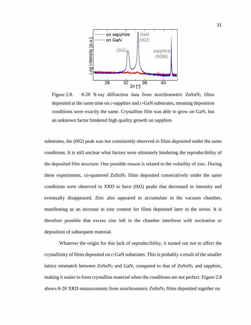
making it easier to form crystalline material when the conditions are not perfect. Figure 2.8
shows θ-2θ XRD measurements from stoichiometric ZnSnN2 films deposited together on
Figure 2.8. θ-2θ X-ray diffraction data from stoichiometric ZnSnN2 films
deposited at the same time on c-sapphire and c-GaN substrates, meaning deposition
conditions were exactly the same. Crystalline film was able to grow on GaN, but
an unknown factor hindered high quality growth on sapphire.

32
Figure 2.9. θ-2θ X-ray diffraction data from ZnSnN2 films deposited with 60 W
zinc plasma power and varying tin plasma power. (002) peak loses intensity and
broadens as the tin power is decreased and film composition deviates further away
from stoichiometry (Figure 2.3a).
Figure 2.10. θ-2θ X-ray diffraction data from ZnSnN2 films with varying gas
pressure and zinc/tin plasma powers of (a) 60/110 W and (b) 120/210 W. (002)
peak loses intensity and broadens as gas pressure is increased. Deposition using
higher power results in mostly amorphous material.
33 c-sapphire and c-GaN, meaning all of the deposition conditions were exactly the same. The
film on c-GaN is crystalline and textured with a very sharp (002) peak around 32.4°, while
the film on c-sapphire is amorphous or possibly nanocrystalline. As a result, a few studies
were carried out to examine the structural effect of varying deposition conditions using
only c-GaN substrates. XRD measurements from the same samples examined in Figure
2.3a are shown in Figure 2.9. As the film composition moves further away from
stoichiometry, the (002) peak loses intensity and broadens, indicating that the material
structure is becoming increasingly disordered. Similarly, XRD from the samples examined
in Figure 2.5a are shown in Figure 2.10a-b. For films deposited with 60 W zinc plasma
power, the (002) peak loses intensity and broadens as the gas pressure is increased.
Figure 2.11. Transmission electron microscope bright field image of ZnSnN2 on
c-sapphire substrate viewed in cross-section. Grains are columnar and less than 50
nm wide, which is typical for sputtered material.

34
The resulting increase in oxygen incorporation in the films likely forms an abundance of
defects in the crystal structure, which causes the change in the peak shape. When the power
is increased to 120 W zinc plasma power, the XRD measurements reveal that the material
is mostly amorphous, even though the oxygen content is lower in these films. The higher
plasma power may cause the substrate and growing film to be bombarded by higher energy
sputtered molecules that can disrupt the crystal structure.
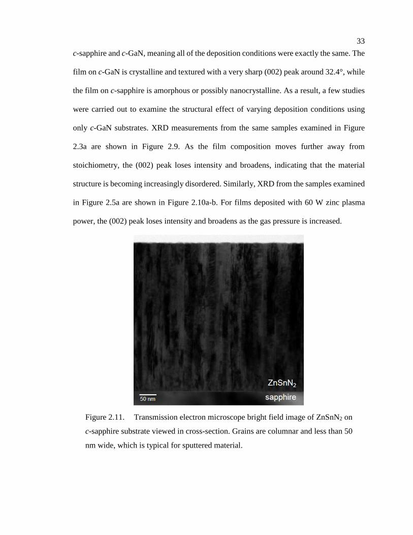
Transmission electron microscopy was also used to study the morphology of the
films. Figure 2.11 shows a TEM bright field image of a cross-sectional sample of ZnSnN2
deposited on a c-sapphire substrate. The film clearly consists of columnar grains that are
less than 50 nm wide. The grain size also appears to increase towards the surface of the
film as grains coalesce during growth. SAED from the same film’s interface (Figure 2.12a)
Figure 2.12. Selected area electron diffraction patterns from the interface of
ZnSnN2 films on (a) c-sapphire and (b) c-GaN substrates. Diffraction spots indicate
that the c-plane in ZnSnN2 is aligned to the c-plane of sapphire and of GaN.
Additionally, (1010) substrate planes are aligned with (100) and (010) ZnSnN2
planes on sapphire and only with (010) ZnSnN2 planes on GaN. Miller indices in
yellow belong to ZnSnN2 and indices in blue belong to the substrate.
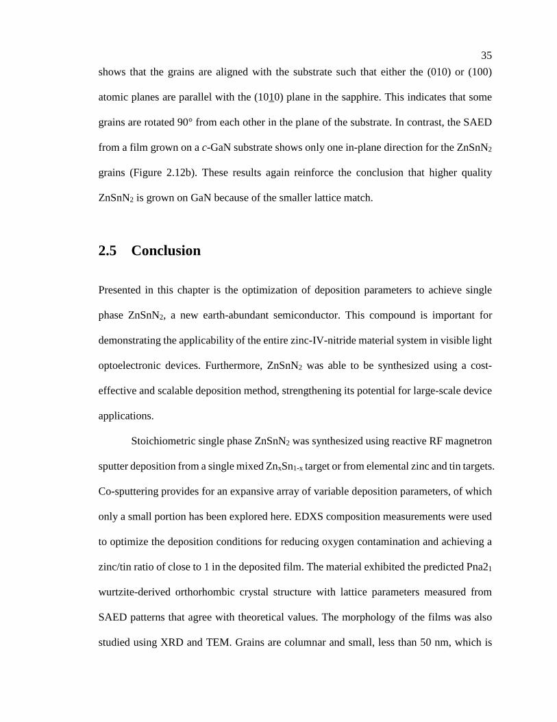
35 shows that the grains are aligned with the substrate such that either the (010) or (100)
atomic planes are parallel with the (1010) plane in the sapphire. This indicates that some
grains are rotated 90° from each other in the plane of the substrate. In contrast, the SAED
from a film grown on a c-GaN substrate shows only one in-plane direction for the ZnSnN2
grains (Figure 2.12b). These results again reinforce the conclusion that higher quality
ZnSnN2 is grown on GaN because of the smaller lattice match.
2.5 Conclusion
Presented in this chapter is the optimization of deposition parameters to achieve single
phase ZnSnN2, a new earth-abundant semiconductor. This compound is important for
demonstrating the applicability of the entire zinc-IV-nitride material system in visible light
optoelectronic devices. Furthermore, ZnSnN2 was able to be synthesized using a cost-
effective and scalable deposition method, strengthening its potential for large-scale device
applications.
Stoichiometric single phase ZnSnN2 was synthesized using reactive RF magnetron
sputter deposition from a single mixed ZnxSn1-x target or from elemental zinc and tin targets.
Co-sputtering provides for an expansive array of variable deposition parameters, of which
only a small portion has been explored here. EDXS composition measurements were used
to optimize the deposition conditions for reducing oxygen contamination and achieving a
zinc/tin ratio of close to 1 in the deposited film. The material exhibited the predicted Pna21
wurtzite-derived orthorhombic crystal structure with lattice parameters measured from
SAED patterns that agree with theoretical values. The morphology of the films was also
studied using XRD and TEM. Grains are columnar and small, less than 50 nm, which is
36 typical of sputtered material. The choice of substrate also played a large role in making
high quality material. The smaller lattice mismatch to GaN, compared to sapphire, allowed
for growth of highly crystalline and textured ZnSnN2 films that were strained at the
interface to match with the lattice of the substrate.
In the next chapter, exploration of the zinc-IV-nitride material system will be
extended by alloying ZnSnN2 with ZnGeN2, resulting in an earth-abundant tunable
bandgap semiconductor that spans a majority of the visible spectrum. Optical properties of
these alloys will be characterized to determine if they can potentially serve as an alternative
to InxGa1-xN in optoelectronic devices.

37
Chapter 3
Tunable Bandgap ZnSnxGe1-xN2 Alloys
In recent years, InxGa1-xN alloys have attracted attention in the scientific community
because of their demonstrated success in optoelectronic devices, especially those that
interact with visible light such as light-emitting diodes (LEDs) and photovoltaics. For such
applications, InxGa1-xN is ideal because the direct bandgap is tunable over a theoretical
range of 0.7 eV to 3.4 eV by changing the amount of indium in the alloy, and high quality
material can be grown with large absorption coefficients and mobilities. However,
InxGa1-xN alloys with high indium content have been difficult to grow because InN and
GaN have a large difference in lattice parameters, leading to indium segregation and phase
separation. Extensive research has been conducted in pursuit of overcoming this problem
so that the entire theoretical bandgap range can be accessed. Incorporating more than about
30% indium into the alloy results in phase separation, which limits the bandgap to the blue
range of the visible spectrum. This is generally referred to as the “green gap” in the LED
industry, as researchers have been unable to produce an efficient green LED that emits
between 520 and 530 nm. Even though there are more sophisticated growth strategies for
InxGa1-xN that allow for near-green emission, such as quantum well structures, the scarcity
and cost of indium will limit its large-scale deployment.
38 Based on theoretical predictions, earth-abundant ZnSnxGe1-xN2 is expected to have
similar optical and electronic properties to InxGa1-xN [7], and can potentially be tuned to
span an energy range of 1.4 eV to 2.9 eV, which still covers the majority of the visible
spectrum. Although the alloy has a shorter range of predicted bandgaps, it also has a smaller
lattice mismatch between its constituent materials, ZnSnN2 and ZnGeN2. This is a potential
advantage for alloying because the large lattice mismatch is a major factor contributing to
the phase separation of InN and GaN. If phase separation does not occur, ZnSnxGe1-xN2
could be capable of closing the “green gap.” Additionally, an efficient graded or multi-
junction photovoltaic device could be developed with any combination of bandgaps
between 1.4 eV to 2.9 eV. One simply needs to search the literature for InxGa1-xN to have
an idea of the range of optoelectronic devices that could benefit from an earth-abundant
alternative.
In this chapter, ZnSnxGe1-xN2 is synthesized by adding germanium to the sputtering
process described in Chapter 2. A wide range of compositions with the correct zinc and
nitrogen stoichiometry can be accessed using this method. X-ray diffraction (XRD)
measurements show a linearly shifting (002) peak, indicating no phase separation.
Spectroscopic ellipsometry reveals optical bandgaps that increase with increasing
germanium incorporation from about 1.8 to 3.1 eV.
3.1 Linear Incorporation of Germanium to Form ZnSnxGe1-xN2
ZnSnxGe1-xN2 thin films were deposited on c-sapphire and c-GaN substrates by reactive
radio frequency (RF) co-sputtering from metal targets in an argon/nitrogen plasma. The
39 gas pressure was held at 3 mTorr during deposition with 75% nitrogen in the plasma. To
encourage crystalline growth, the substrate temperature was set to about 270 °C. For
ZnSnxGe1-xN2 with x = 0 or 1, films were deposited by co-sputtering from zinc (99.99%)
and germanium (99.999%) or zinc and tin (99.999%) elemental targets, all obtained from
the Kurt J. Lesker Company. An RF power of 44 W was applied to the zinc target, while
the tin and germanium targets required 74 W and 104 W, respectively, to obtain
stoichiometric films as determined by energy dispersive X-ray spectroscopy (EDXS).
Films with 0 < x < 1 were sputtered from a Zn0.75Sn0.25 pressed powder target (99.99%,
ACI Alloys, Inc.) and a germanium elemental target because the sputtering system was
limited to two RF power supplies at the time of these experiments. The combined target is
zinc-rich because the high vapor pressure of zinc limits its incorporation during deposition
at substrate temperatures above about 200 °C (see Chapter 2). For the data presented here,
the RF power on the Zn0.75Sn0.25 target was kept at 134 W and the power applied to the
germanium target was varied from 30 W to 134 W to create a set of samples with ranging
compositions. As shown in Chapter 2, the combined target requires a higher power than
the elemental targets to get a comparable deposition rate that limits oxygen incorporation
in the film.
3.1.1 Measurements of Composition Variation
Figure 3.1 presents the composition measurements for ZnSnxGe1-xN2 films on c-sapphire
and c-GaN substrates using EDXS. An accelerating voltage of less than 10 kV was used to
confine the size of the activation volume to the thickness of the thin films. All of the
samples have close to 25 at% zinc and 50 at% nitrogen within error. The quaternary films

40
on c-sapphire have x values of 0.71 ± 0.07, 0.51 ± 0.06, 0.40 ± 0.05, and 0.37 ± 0.04,
corresponding to germanium RF powers of 44 W, 74 W, 104 W, and 134 W, respectively.
The films on c-GaN have x values of 0.88 ± 0.03, 0.81 ± 0.02, 0.61 ± 0.02, 0.50 ± 0.02,
and 0.36 ± 0.01, corresponding to germanium RF powers of 30 W, 44 W, 60 W, 104 W,
and 134 W, respectively. The value of x was calculated by taking the ratio of atomic percent
tin to the total atomic percent of group IV elements.
Figure 3.1. Composition of ZnSnxGe1-xN2 films deposited on (a) c-sapphire and
(b) c-GaN substrates measured by energy dispersive X-ray spectroscopy. Films on
each substrate exhibit consistent zinc and nitrogen concentrations close to 25 at%
and 50 at%, respectively. Various tin and germanium concentrations are
demonstrated, allowing for characterization of a wide range of alloy compositions.

41
3.1.2 X-ray Diffraction Studies of Phase Separation
Verification of the structure and phase of sputtered ZnSnN2 (x = 1) was described in
Chapter 2, and a similar examination was done to confirm that the structural properties of
the ZnGeN2 (x = 0) deposited here agreed with the literature. Films on c-GaN substrates
were measured by θ-2θ XRD using copper Kα radiation (λ = 1.54 Å) over a 2θ range of
25° to 45°. The ZnGeN2 films presented one prominent peak at 2θ = 34.1°, confirmed as
the (002) reflection by calculations based on theoretical lattice parameters [7]. The
corresponding experimental c lattice parameter calculated using Equation (2.1) is 5.25 ±
0.01 Å for the ZnGeN2 deposited by reactive RF sputtering. This value is slightly larger
than the experimental values reported in the literature, which range from 5.12 to 5.20 Å
[29], and even includes measurements of other sputter deposited ZnGeN2 [17]. Kikkawa et
al. attributes the slightly larger parameter of their material to excess nitrogen incorporation
during sputtering, and the same process may be involved here.
The structure of the ZnSnxGe1-xN2 films was also studied using XRD to determine
whether the material was a continuous alloy or if it was a mixture of different phases.
Simply by switching from ternary materials to a quaternary alloy, the variability in the
deposition process increases significantly. It was therefore important to ensure that other
nitride or oxide phases were not being created, especially ones that would indicate phase
separation of the alloys. The intermediate compositions of single phase ZnSnxGe1-xN2 were
expected to have XRD peaks with 2θ positions in between those of ZnSnN2 and ZnGeN2,
in accordance with Vegard’s law. On c-sapphire substrates, two peaks were observed in
each film corresponding to the (002) and (211) or (021) reflections, meaning the films are

42
Figure 3.2. θ-2θ X-ray diffraction data from ZnSnxGe1-xN2 films deposited on
(a) c-sapphire and (b) c-GaN substrates. (c) All films have a prominent (002) peak
whose position shifts linearly with composition, x. Peaks are identified by Miller
indices assigned based on theoretical unit cell calculations. Error bars indicate
statistical error calculated by peak-fitting software.

43 highly polycrystalline with the grains oriented in different directions. On c-GaN substrates,
a strong (002) reflection coupled with weak peaks or no peaks in any other crystallographic
directions indicated that the films are strongly textured with the (001) planes parallel to the
surface of the substrate. Figure 3.2a-b displays the XRD θ-2θ scans around the (002)
reflection for films with various compositions grown on c-sapphire and c-GaN substrates.
The (002) peak position increases steadily with increasing germanium content, indicating
that there is no apparent phase separation in the material. This result contrasts with
InxGa1-xN alloys, where the large lattice mismatch between InN and GaN causes the indium
to segregate for alloys with high indium content, resulting in phase separation and
formation of distinct domains of InN and GaN. An XRD measurement for phase separated
InxGa1-xN would therefore show two separate peaks representing the two different lattice
parameters present in the material. In the ZnSnxGe1-xN2 case, there is only one prominent
peak in the 2θ range of the (002) reflection, and for films with 0 < x < 1 there are no peaks
at the 2θ positions of ZnSnN2 or ZnGeN2. This singular (002) peak reinforces the
conclusion that the material is continuous and not a mixture of different phases.
Additionally, the 2θ position of the (002) peak increases constantly with increasing
germanium content, meaning that the unit cell continuously expands and contracts as the
composition is changed such that each composition creates a unique material. This result
is promising because it suggests that the entire range of bandgap values should be
accessible without the need for more complicated growth strategies. Figure 3.2c further
highlights the continuous alloying of the films by showing that the relationship between
the (002) peak position and composition is linear. Consequently, the c lattice parameter
decreases linearly with increasing germanium content. Data from many samples with
44 various compositions are shown, with a linear fit of the data for films grown on c-GaN.
The films grown on GaN are of higher crystalline quality because the lattice mismatch
between GaN and ZnSnxGe1-xN2 is about half of the mismatch between sapphire and
ZnSnxGe1-xN2.
3.2 Optical Bandgap and Absorption Properties
The continuously shifting 2θ position of the (002) peak with changing composition,
exhibited in these ZnSnxGe1-xN2 thin films, essentially points to alloying of the material
with no observable phase separation according to the XRD analysis. The reason the growth
of these materials does not suffer from the same difficulties as InxGa1-xN growth is likely
because the difference in lattice parameter between ZnSnN2 and ZnGeN2 is about half as
large as the difference between InN and GaN. Therefore, ZnSnxGe1-xN2 is able to
accommodate a larger range of compositions without straining the lattice to a point where
phase separation is favorable. This result is valuable because it suggests that the entire
range of predicted bandgaps for ZnSnxGe1-xN2 should be easily accessible by tuning the
ratio of the group IV elements.
To study the bulk electronic structure of these materials, spectroscopic ellipsometry
measurements were made to reveal features in the joint density of states, particularly the
optical absorption edge. The system, from SENTECH, uses a xenon lamp visible light
source and a Fourier-transform infrared spectrometer to access wavelengths of 250 nm < λ
< 2300 nm. The angle of incident light was varied between 50°, 60°, and 70° from the
surface normal to improve the accuracy of the fitting algorithm. Only films grown on c-
sapphire were measured with this method because avoiding the additional GaN layer
45 ensured that the fitting model was as simple as possible. Although the transparency of
sapphire caused some issues involving multiple reflections, this could often be mitigated
by measuring thicker films. Output data from the ellipsometer consists of the amplitude
(Ψ) and phase (Δ) of the change in polarization due to interaction with the material. The
wavelength-dependent refractive index (n) and extinction coefficient (k) were fit from the
measured Ψ and Δ at 1 nm intervals assuming an isotropic film. k(λ) was then used to
calculate the absorption coefficient using 𝛼𝛼(𝑛𝑛) = 4𝜋𝜋𝜋𝜋(𝑛𝑛) ⁄ 𝑛𝑛 . For direct bandgap
semiconductors, a plot of the square of the absorption coefficient versus photon energy can
be linearly extrapolated to the energy axis to estimate the value of the optical bandgap.
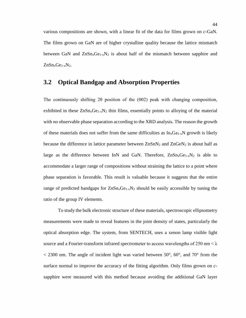
Because ZnSnN2 was a new material, it was first important to characterize the
optical properties alone before alloying with ZnGeN2. An example of the extracted n(λ)
and k(λ) data for a thick ZnSnN2 film is shown in Figure 3.3. From this data, it can be
shown that the material is highly absorbing, with α > 104 cm-1 over the entire visible range.
Figure 3.3. Refractive index, n(λ), and extinction coefficient, k(λ), extracted
from spectroscopic ellipsometry measurements of a representative ZnSnN2 film.
k(λ) has a minimum value greater than zero due to defect absorption.
46
It should also be noted that the extinction coefficient of the measured film never reaches
zero. For an ideal material with an optical bandgap, there should be zero absorption for
energies below that gap. One possible explanation for this result is that the deposited
material will always exhibit a low level of defect absorption because the data in Figure 3.3
was obtained from a predominantly amorphous film. Various films with thicknesses
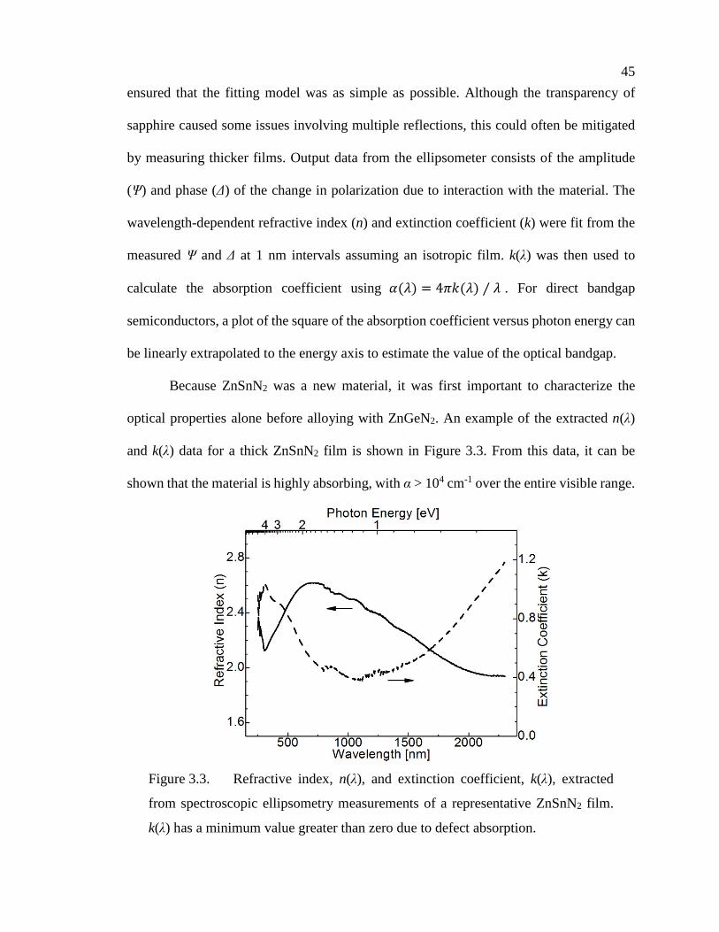
between 1.5 and 3 μm were analyzed, and the plots of squared absorption coefficient vs.
Figure 3.4. Optical bandgap estimation for ZnSnN2. (a) Squared absorption
coefficient vs. photon energy for six stoichiometric ZnSnN2 samples. Data was
linearly extrapolated near the absorption edge to estimate an optical bandgap
energy of about 1.8 to 2.1 eV. (b) θ-2θ X-ray diffraction data of the same films
represented in (a). Samples with similar absorption spectra also have a similar
crystal structure.

47 photon energy are shown in Figure 3.4a. All samples were stoichiometric and deposited
under optimized growth conditions by co-sputtering. A linear fit of the data near the
absorption edge reveals a direct optical bandgap of about 1.8 to 2.1 eV. Theoretical
predictions for the fundamental bandgap of ZnSnN2 range from 1.4 to 2.1 eV [3-5]. One
point of note in Figure 3.4a is that although the extrapolated optical bandgap values are
similar, the absorption coefficients vary significantly between samples. In analyzing this
further, it was discovered that the differences in absorption properties were related to the
crystallinity of the material. Figure 3.4b displays the θ-2θ XRD scans of the same samples
as indicated. The samples with similar absorption properties also have similar peak patterns
in XRD. Additionally, the magnitude of the absorption increases as the (002) peak broadens.
The exact mechanism for this effect is not known, but may be related to speculations that
the degree of cation disorder can affect the bandgap of ZnSnN2 [4].
The optical bandgap of the ZnGeN2 deposited here was also measured to confirm
agreement with literature values. The plot of squared absorption coefficient vs. photon
energy for two of these samples is displayed in Figure 3.5. The oscillations in the data are
most likely due to thin film interference effects as these films were less than 500 nm thick.
The extrapolated optical bandgap is about 3.1 eV, which is in agreement with previous
measurements of sputtered material [17]. ZnGeN2 grown by other methods has reported
bandgap values between 2.7 and 3.4 eV [29].
Finally, the optical bandgap extrapolations for ZnSnxGe1-xN2 films with 0 < x < 1
are shown in Figure 3.6. The absorption exhibits a blue-shift as the germanium content is
increased, and is bounded by the data from ZnSnN2 and ZnGeN2. Like alloying between
other nitride semiconductors, the shift is not linear with the change in composition. The

48 accuracy of these measurements is also obscured by the large band tails near the absorption
edge in all of the samples. These are likely due to defect absorption, as sputter deposition
is not the highest quality semiconductor growth method, and XRD measurements indicate
that the films are polycrystalline. Nevertheless, the absorption varies enough with
composition that accessing all of the bandgap values between 1.8 and 3.1 eV is feasible
with ZnSnxGe1-xN2, including the bandgap energy corresponding to green light. This
suggests that the “green gap” could be closed with better control of the composition of
these materials.
3.3 Conclusion
Presented in this chapter is the investigation of tunable bandgap ZnSnxGe1-xN2 alloys and
the characterization of their optical properties. These new materials are predicted to have
Figure 3.5. Optical bandgap estimation for ZnGeN2. Squared absorption
coefficient vs. photon energy for two ZnGeN2 samples. Data was linearly
extrapolated near the absorption edge to estimate an optical bandgap energy at
about 3.1 eV.
49 optoelectronic properties that are similar to those of InxGa1-xN, suggesting applications as
an earth-abundant alternative to current III-nitride materials.
Thin film growth of ZnSnxGe1-xN2 alloys was demonstrated using reactive RF co-
sputter deposition. The alloy composition (x) was varied by only changing the plasma
power applied to one of the metal targets. Results from θ-2θ XRD measurements show that
the (002) peak position linearly increases in 2θ with decreasing x over a wide range of
compositions. Furthermore, no additional peaks were observed belonging to a different
ZnSnxGe1-xN2 phase or any other nitrides or oxides. The conclusion drawn from this data
is that ZnSnxGe1-xN2 does not phase separate in the same way that InxGa1-xN does. As a
result, the bandgap of ZnSnxGe1-xN2 alloys should also be tunable over the entire range of
x from ZnGeN2 to ZnSnN2. In fact, data extracted from spectroscopic ellipsometry
measurements showed that the optical bandgap of the samples grown here is tunable from
about 1.8 eV to 3.1 eV. This range includes the bandgap correlating to emission of green
light with a wavelength of 520-530 nm, suggesting that ZnSnxGe1-xN2 alloys can
potentially overcome the “green gap” that has become an obstacle for traditional
semiconductors. Furthermore, the exploration of additional alloy compositions would be
better facilitated by more accurate bandgap measurements. If spectroscopic ellipsometry
continues to be the characterization method of choice, reducing defects in the material
could decrease band tails at the absorption edge, and ensuring an adequate film thickness
could reduce thin film interference effects. Photoluminescence (PL) is also a common
method for measuring bandgap states. Previous attempts to measure PL from these
materials was unsuccessful, although Quayle et al. have observed PL excitation from
ZnSnN2 grown using a plasma assisted vapor-liquid-solid technique [20]. A fit of their PL

50 excitation spectra suggests a band gap of 1.7 ± 0.1 eV, while the peak in the PL spectrum
is around 1.4 eV. It is unclear if the peak value is due to defect luminescence or if it
represents the intrinsic band gap energy [20].
One important result that came out of this study was the measurement of the optical
bandgap for ZnSnN2, which had not be experimentally characterized before. Values ranged
from 1.8 to 2.1 eV, and the absorption properties appeared to be strongly dependent on the
crystallinity of the material. These bandgap values tend to agree with predictions made by
Punya et al. [5] and Feldberg et al. [4], who both arrived at a bandgap of about 2 eV using
Figure 3.6. Optical bandgap estimation for ZnSnxGe1-xN2 alloys. Squared
absorption coefficient vs. photon energy for ZnSnxGe1-xN2 samples with a range of
compositions, x. Data was linearly extrapolated near the absorption edge to estimate
optical bandgap energies that increase as x decreases.

51 density functional theory. Without any other experimental data to compare to, the best
option for evaluating ZnSnN2 results is to refer to the literature for InN. For many years,
the accepted bandgap of InN was about 2 eV, originally observed in sputtered InN. The
true fundamental bandgap of about 0.7 eV was only recently discovered by using molecular
beam epitaxy, which grows a higher purity material [30]. This discrepancy is generally
attributed to oxygen contamination and filling of the conduction band by excess electrons.
Because ZnSnN2 was also deposited by sputtering and has a predicted electronic structure
similar to that of InN, the fundamental bandgap of the material may be closer to another
prediction made by Lahourcade et al. of 1.4 eV [3]. If the bandgap is actually much lower
than 2 eV, then the tunable range of ZnSnxGe1-xN2 could be expanded significantly.
Confirming the real bandgap, however, will require synthesis of high purity ZnSnN2 by a
method such as molecular beam epitaxy or metalorganic chemical vapor deposition.
The following chapter will examine the interaction between the optical and
electronic properties of ZnSnxGe1-xN2 alloys. In particular, investigations of the electronic
structure of ZnSnN2 were carried out to determine if any features could have a significant
effect on the absorption edge observed with spectroscopic ellipsometry.

52
Chapter 4
Bulk Electronic Properties of ZnSnxGe1-xN2
Good electronic properties are essential to the efficacy of semiconductor devices.
Optoelectronic devices rely not only on strong interaction with light, but also on the
capacity to transport charge efficiently. For devices implementing p-n junctions, the ability
to dope a semiconductor is also very valuable. III-nitride materials have come to be
recognized as favorable materials for such applications, mostly because they have tunable
bandgaps with direct transitions. The polar wurtzite crystal structure of III-nitrides also
allows for certain attributes that could be advantageous in devices such as piezoelectricity
and non-linear optical properties, which are not observed in other common semiconductors
like silicon and GaAs. The zinc-IV-nitride materials are predicted to have crystal and
electronic structures similar to those of the III-nitrides, so the same device advantages
could be expected for these new earth-abundant compound semiconductors.
Results from the previous chapter revealed that the bandgap of sputter deposited
ZnSnxGe1-xN2 alloys was tunable over a range of about 1.8 to 3.1 eV. Measurements also
indicated that these materials are highly absorbing, although the absorption is slightly
decreased as the bandgap increases. In this chapter, the ZnSnxGe1-xN2 alloys are explored
further by characterizing their bulk electronic properties, specifically by measuring the
carrier transport properties. ZnSnN2 is found to be unintentionally doped with electron

53 densities as high as 1022 cm-3, likely incurring a Burstein-Moss shift. ZnGeN2, on the other
hand, was too resistive to make any carrier transport measurements. Discussion of the
relationship between optical and electronic properties in zinc-IV-nitride materials will also
be presented in this chapter to understand their potential for use in optoelectronic devices.
4.1 Making Ohmic Contacts
Electrical contacts are the method through which semiconductor materials and devices
interact with external systems. Contacts can be ohmic or non-ohmic (rectifying), where
ohmic contacts are defined as having a linear current-voltage relation, as described by
Ohm’s law. In making measurements of electronic properties, and thinking ahead towards
device design, it is essential that contacts have ohmic character so as not to interfere with
the behavior of the material being studied. Discovery and preparation of ohmic contacts
can be a formidable task, as evidenced by the amount of research effort dedicated to the
subject. The Schottky-Mott model predicts that a metal will form an ohmic contact with a
given n-type semiconductor if the metal work function is less than the electron affinity of
the semiconductor. Similarly, for p-type semiconductors, the metal work function much be
larger than the sum of the electron affinity and bandgap of the semiconductor to make an
ohmic contact. It turns out that this model does not describe real material interactions very
well, but it is nonetheless a good starting point. Beyond simply choosing an appropriate
metal work function, fabrication of contacts often requires deposition of multiple layers
and additional annealing steps to achieve the desired ohmic behavior. For these reasons,
preparation of reliable ohmic contacts is often considered an art form and is a major focus
of studies on III-V device fabrication.

54
Common contacting metals were tested to determine if an ohmic contact could be
developed for ZnSnxGe1-xN2 alloys. These included gold, platinum, aluminum, nickel, and
titanium. Metals were deposited by sputtering or e-beam evaporation on opposite edges of
ZnSnxGe1-xN2 films in preparation for measurement on a 2-point probe station. No
annealing or additional preparation was performed on the contacted films. The resulting
current-voltage curves from two different compositions of ZnSnxGe1-xN2 are shown in
Figure 4.1. All of the metals form an ohmic contact to the samples that were tested. This
result suggests that ZnSnxGe1-xN2 either has an electron affinity greater than 5 eV, which
Figure 4.1. Current-voltage measurements of metal contacts on ZnSnxGe1-xN2
films with compositions of (a) x = 0.36 and (b) x = 0.88. All metals make ohmic
contact with the samples, indicated by linearly-shaped curves.

55 is the largest metal work function tested, or a Fermi energy that lies above the conduction
band edge.
The next section will discuss characterization of the carrier transport properties of
ZnSnxGe1-xN2 films. The results will support the hypothesis that the Fermi energy of these
materials lies within the conduction band, indicative of a degenerate semiconductor.
4.2 Majority Carrier Transport Properties
The ability to transport charge efficiently is a hallmark of semiconductor materials that are
widely used in device applications. To assess the suitability for optoelectronic devices, the
transport properties of majority carriers in ZnSnxGe1-xN2 alloys were characterized with
resistivity and Hall effect measurements. Films are found to have characteristics of
degenerately doped semiconductors, most likely resulting from the use of sputtering as a
deposition method.
4.2.1 Resistivity Measurements
In-plane resistivity measurements were conducted on various ZnSnxGe1-xN2 films using
both four-point probe and van der Pauw geometries. A plot of the data is shown in Figure
4.2 as a function of the alloy composition, x. Resistivity was so large in ZnGeN2 that no
current could be passed through the samples for measurement. For all other sample
compositions, the resistivity appears to increase exponentially with increasing germanium
content spanning nine orders of magnitude, from 10-3 to 105 Ω∙cm. These values are
somewhat lower than those of typical semiconducting materials. For example, silicon

56 resistivity is on the order of 102 Ω∙cm and that of GaAs can range from 10-1 to 108 Ω∙cm.
The exponential relationship is likely related to the shifting electronic band structure as the
composition of the alloys is varied. If the Fermi level remains at a constant energy and the
conduction band increases in absolute energy with increasing germanium content, an
exponential trend in resistivity would be observed.
Also consistent with the expectation for semiconducting material, results show that
the resistivity of ZnSnxGe1-xN2 films decreases with increasing temperature [31]. However,
only films with very low tin content demonstrate the expected exponential relationship.
Alloys with higher tin content exhibit a negative linear relationship between resistivity and
temperature. The resistivity of metals is also known to shift linearly with temperature,
although the direction of the trend is opposite to that of the ZnSnxGe1-xN2 films measured
here. This may indicate that the materials under investigation behave in both metallic and
semiconducting manners depending on the composition and growth conditions.
Figure 4.2. Resistivity of ZnSnxGe1-xN2 films. Data was collected using four-
point probe and van der Pauw geometries. Resistivity exponentially increases with
increasing germanium content.

57
4.2.2 Carrier Density and Mobility
Hall effect measurements were used to estimate the density and mobility of bulk
majority carriers in ZnSnxGe1-xN2 films. Samples were cut into small squares with
dimensions of approximately 6 × 6 mm, and ohmic contacts (platinum or gold) were e-
beam evaporated onto the corners through a shadow mask. A schematic of the
measurement geometry is shown in Figure 4.3. The prepared samples were contacted on a
probe station in a van der Pauw configuration and placed into a 14000 G magnetic field.
Current was flowed through contacts on opposite corners of the sample perpendicular to
the magnetic field direction. The field exerts a Lorentz force on the carriers in the direction
orthogonal to those of the field and current flow. Charge is then built up on opposite sides
of the sample to balance
Figure 4.3. Schematic of Hall effect measurement geometry. Square samples
were prepared with contacts on each corner. When current (I13) is flowed through
opposite corners in the presence of a magnetic field (B), a voltage (VH) can be
measured across the remaining two contacts.

58 the effect of the Lorentz force, resulting in a measurable voltage, or Hall voltage, across
the remaining two sample contacts. The sign of the Hall voltage indicates the type of carrier
being observed, and can be used to calculate the carrier mobility. Together with the van
der Pauw resistivity measurements, the carrier density can also be calculated.
Results from Hall effect measurements of ZnSnN2 generated very high carrier
concentrations on the order of 1020-1022 cm-3 with mobilities between 1 and
20 cm2∙V-1∙s-1, placing these materials well within the range of degenerately doped
semiconductors. These results are in agreement with previous resistivity and ohmic contact
experiments that indicate the sputtered ZnSnN2 is essentially acting like a metal rather than
a semiconductor. Measurements were also rather inconsistent in determining the carrier
type, possibly because of the low mobilities or existence of multiple carrier types. However,
the hot-point probe technique, where a current is measured from the flow of majority
carriers away from a heat source, was utilized to show that electrons were the majority
carriers.
The cause of the high unintentional doping is still unknown, but is likely related to
excess defects in the material that result from the deposition method. Based on the
examination of unintentional degenerate doping in InN, the leading suspects are nitrogen
vacancies and oxygen impurities. In ZnSnN2, an abundance of tin on zinc antisite defects
could also contribute electrons to the material [32]. The mobility is likely hindered by the
large carrier density due to ionized impurity scattering, but additional impedance can be
caused by grain boundaries, which have been shown to act as scattering centers in InN [33].
The Hall effect only probes carrier transport that is parallel to the surface of the film. Due

59
Figure 4.4. (a) Carrier density and (b) mobility for ZnSnxGe1-xN2 films
measured using the Hall effect. Results were inconsistent in determining the charge
of the majority carriers for some compositions. Carrier density appears to decrease
with increasing germanium content, but mobilities are not affected by the film
composition.

60 to the columnar film structure, as seen in Figure 2.11, the carriers must encounter numerous
grain boundaries during these Hall effect measurements.
If the observed degenerate doping is the result of the deposition method, ZnGeN2
should also exhibit large carrier concentrations with low mobilities. In fact, electron
concentrations of 1018-1019 cm-3 were reported by Larson et al. with mobilities of 0.5-5
cm2∙V-1∙s-1 [14]. Unfortunately, the high resistivity of the sputtered ZnGeN2 films studied
here did not allow for accurate determination of the carrier concentrations from Hall effect
measurements. However, this does suggest that there may be some composition on the
spectrum of ZnSnxGe1-xN2 alloys where non-degenerate behavior might be observed.
The Hall effect measurement results for various compositions of ZnSnxGe1-xN2 are
shown in Figure 4.4. The carrier type is still ambiguous for some of the compositions. Only
films with x between 0.5 and 0.7 consistently reported the carrier type as electrons, with
densities on the order of 1019 cm-3 and mobilities between 10-1 and 101 cm2∙V-1∙s-1. These
materials still behave degenerately. Overall, the carrier density does seem to decrease as
the germanium content is increased, but mobilities do not appear to change with the film
composition. This substantiates the claim that the low mobility is predominantly caused by
the morphology of the films and grain boundary scattering rather than ionized impurity
scattering from large carrier densities. As a result, growth of single crystal films or films
with larger grains should show improvements in the mobility measured by the Hall effect.
4.3 Interactions between Optical and Electronic Properties
Due to the nature of the electronic structure of materials, optical properties are closely
related to carrier transport. It is almost impossible to characterize one without referring to
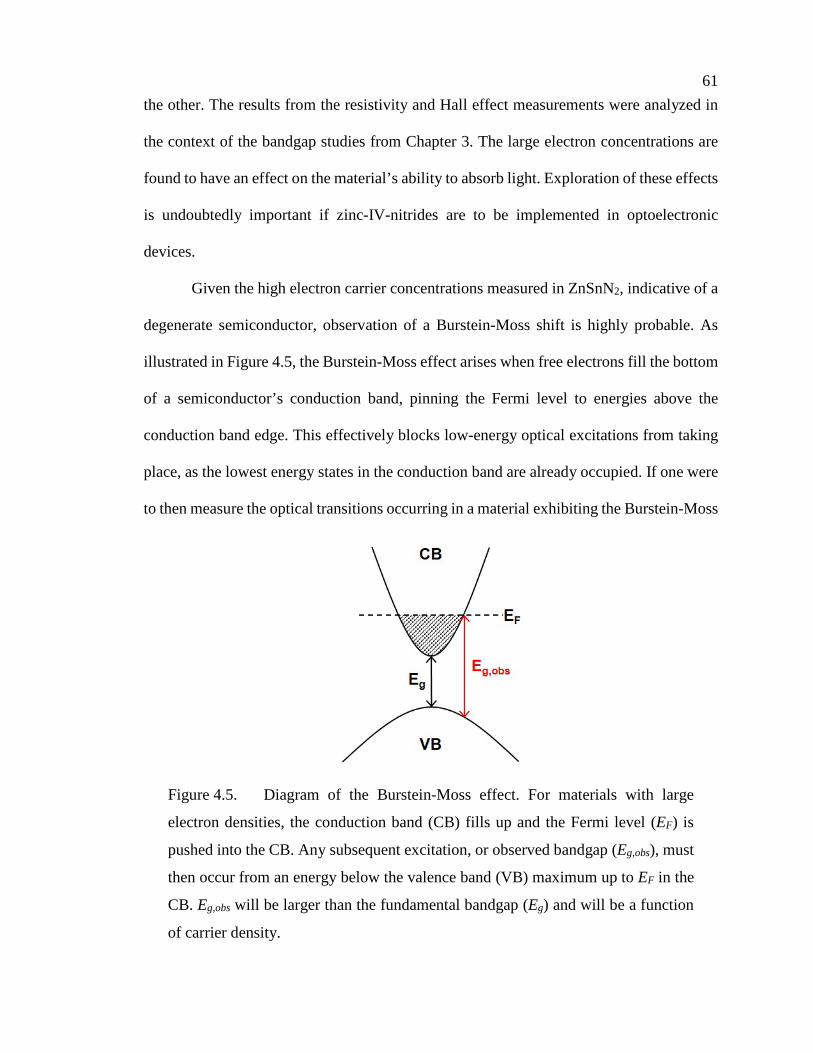
61 the other. The results from the resistivity and Hall effect measurements were analyzed in
the context of the bandgap studies from Chapter 3. The large electron concentrations are
found to have an effect on the material’s ability to absorb light. Exploration of these effects
is undoubtedly important if zinc-IV-nitrides are to be implemented in optoelectronic
devices.
Given the high electron carrier concentrations measured in ZnSnN2, indicative of a
degenerate semiconductor, observation of a Burstein-Moss shift is highly probable. As
illustrated in Figure 4.5, the Burstein-Moss effect arises when free electrons fill the bottom
of a semiconductor’s conduction band, pinning the Fermi level to energies above the
conduction band edge. This effectively blocks low-energy optical excitations from taking
place, as the lowest energy states in the conduction band are already occupied. If one were
to then measure the optical transitions occurring in a material exhibiting the Burstein-Moss
Figure 4.5. Diagram of the Burstein-Moss effect. For materials with large
electron densities, the conduction band (CB) fills up and the Fermi level (EF) is
pushed into the CB. Any subsequent excitation, or observed bandgap (Eg,obs), must
then occur from an energy below the valence band (VB) maximum up to EF in the
CB. Eg,obs will be larger than the fundamental bandgap (Eg) and will be a function
of carrier density.
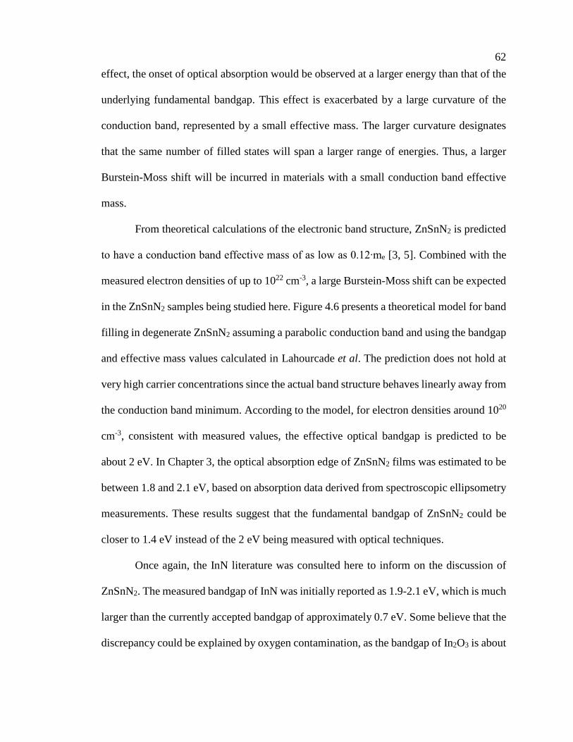
62 effect, the onset of optical absorption would be observed at a larger energy than that of the
underlying fundamental bandgap. This effect is exacerbated by a large curvature of the
conduction band, represented by a small effective mass. The larger curvature designates
that the same number of filled states will span a larger range of energies. Thus, a larger
Burstein-Moss shift will be incurred in materials with a small conduction band effective
mass.
From theoretical calculations of the electronic band structure, ZnSnN2 is predicted
to have a conduction band effective mass of as low as 0.12∙me [3, 5]. Combined with the
measured electron densities of up to 1022 cm-3, a large Burstein-Moss shift can be expected
in the ZnSnN2 samples being studied here. Figure 4.6 presents a theoretical model for band
filling in degenerate ZnSnN2 assuming a parabolic conduction band and using the bandgap
and effective mass values calculated in Lahourcade et al. The prediction does not hold at
very high carrier concentrations since the actual band structure behaves linearly away from
the conduction band minimum. According to the model, for electron densities around 1020
cm-3, consistent with measured values, the effective optical bandgap is predicted to be
about 2 eV. In Chapter 3, the optical absorption edge of ZnSnN2 films was estimated to be
between 1.8 and 2.1 eV, based on absorption data derived from spectroscopic ellipsometry
measurements. These results suggest that the fundamental bandgap of ZnSnN2 could be
closer to 1.4 eV instead of the 2 eV being measured with optical techniques.
Once again, the InN literature was consulted here to inform on the discussion of
ZnSnN2. The measured bandgap of InN was initially reported as 1.9-2.1 eV, which is much
larger than the currently accepted bandgap of approximately 0.7 eV. Some believe that the
discrepancy could be explained by oxygen contamination, as the bandgap of In2O3 is about
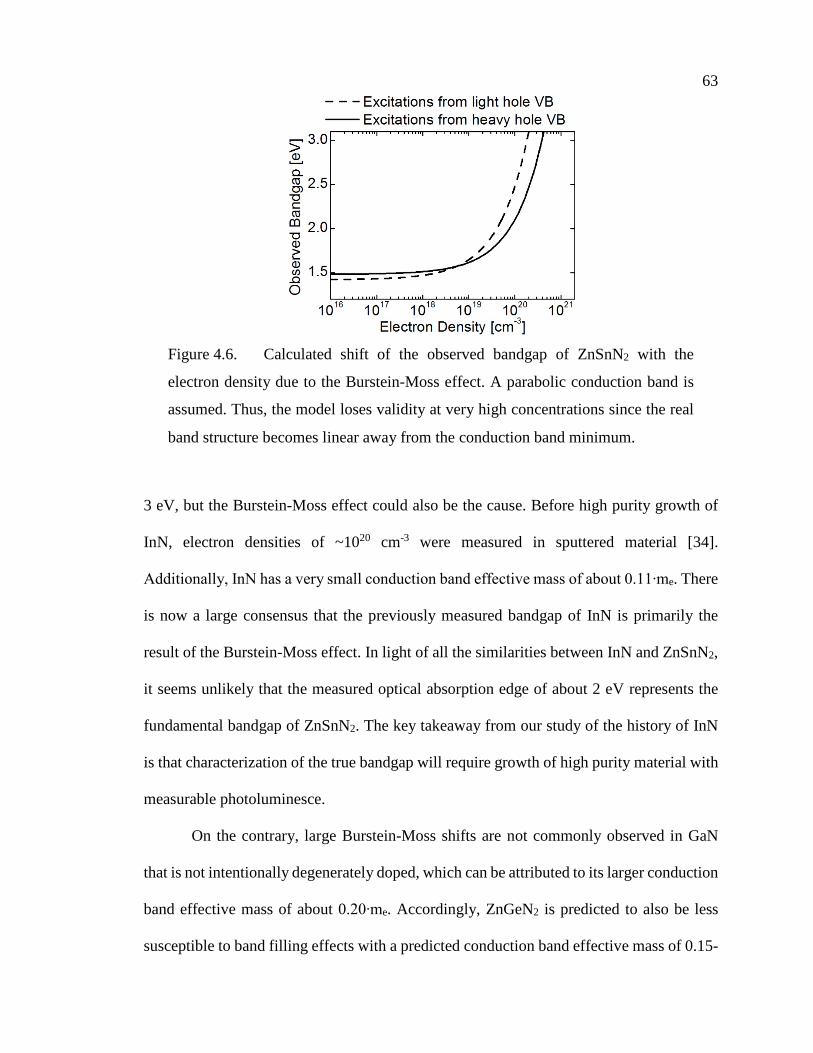
63
3 eV, but the Burstein-Moss effect could also be the cause. Before high purity growth of
InN, electron densities of ~1020 cm-3 were measured in sputtered material [34].
Additionally, InN has a very small conduction band effective mass of about 0.11∙me. There
is now a large consensus that the previously measured bandgap of InN is primarily the
result of the Burstein-Moss effect. In light of all the similarities between InN and ZnSnN2,
it seems unlikely that the measured optical absorption edge of about 2 eV represents the
fundamental bandgap of ZnSnN2. The key takeaway from our study of the history of InN
is that characterization of the true bandgap will require growth of high purity material with
measurable photoluminesce.
On the contrary, large Burstein-Moss shifts are not commonly observed in GaN
that is not intentionally degenerately doped, which can be attributed to its larger conduction
band effective mass of about 0.20∙me. Accordingly, ZnGeN2 is predicted to also be less
susceptible to band filling effects with a predicted conduction band effective mass of 0.15-
Figure 4.6. Calculated shift of the observed bandgap of ZnSnN2 with the
electron density due to the Burstein-Moss effect. A parabolic conduction band is
assumed. Thus, the model loses validity at very high concentrations since the real
band structure becomes linear away from the conduction band minimum.
64 0.22∙me [5]. In fact, the measured optical bandgap for reactively sputtered ZnGeN2 of 3.1
eV is only slightly larger than the theoretical value of 2.9 eV [3], and is actually less than
some experimental measurements of around 3.4 eV that have been reported in the literature
[13, 29]. This suggests that the magnitude of the Burstein-Moss shift will be reduced in
sputtered ZnSnxGe1-xN2 alloys as the germanium content is increased.
4.4 Conclusion
In this chapter, ZnSnxGe1-xN2 alloys were characterized electronically. Results showed that
the resistivity increased exponentially with increasing germanium content. Additionally,
degenerate electron carrier densities of up to 1022 cm-3 were measured, allowing the
materials to make ohmic contact to various high work function metals. The degeneracy of
these materials was also related to the optical characterization from Chapter 3. Large carrier
concentrations are likely to cause a Burstein-Moss shift, which would prevent direct optical
measurement of the fundamental bandgap energy. Therefore, the lower end of the
accessible bandgap energy range of ZnSnxGe1-xN2 alloys may be extended if growth of
higher purity material can be achieved that precludes the Burstein-Moss shift.
One concern with the conclusions drawn in this chapter is that it is unclear whether
the large carrier densities being measured are a bulk effect or if they result from
accumulation of charge at the surface of the films. A technique like capacitance-voltage
(C-V) profiling can provide information about a film’s doping profile. However, C-V
measurements require a rectifying junction, which could not be found in this work. InN
was similarly shown to have large electron carrier densities that disallowed formation of a
rectifying junction with metal contacts. Instead, a KOH-based electrolyte was used as a

65 Schottky contact to perform C-V measurements that implicated a surface charge
accumulation layer [35]. The same technique could prove to be useful in characterizing
ZnSnxGe1-xN2 as well.
Another issue that was encountered in these studies was the low mobility of the
charge carriers, which especially affected the Hall effect measurements. Because of the
nano-scale polycrystalline morphology of the sputter deposited films, the carriers
encounter numerous grain boundaries when travelling in the plane of the film. To overcome
this problem, films that are single crystal or made up of larger grains must be grown.
However, this is not viable if sputtering remains the method of deposition. Further
exploration will require a higher quality growth method, such as molecular beam epitaxy
or metalorganic chemical vapor deposition. Material with better crystalline quality should
also contain fewer defects than sputtered films, resulting in a decrease in the unintentional
doping.
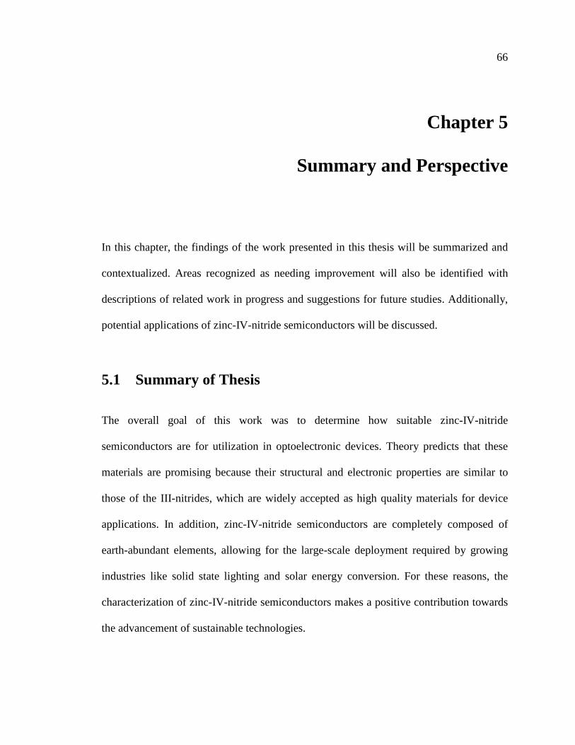
66
Chapter 5
Summary and Perspective
In this chapter, the findings of the work presented in this thesis will be summarized and
contextualized. Areas recognized as needing improvement will also be identified with
descriptions of related work in progress and suggestions for future studies. Additionally,
potential applications of zinc-IV-nitride semiconductors will be discussed.
5.1 Summary of Thesis
The overall goal of this work was to determine how suitable zinc-IV-nitride
semiconductors are for utilization in optoelectronic devices. Theory predicts that these
materials are promising because their structural and electronic properties are similar to
those of the III-nitrides, which are widely accepted as high quality materials for device
applications. In addition, zinc-IV-nitride semiconductors are completely composed of
earth-abundant elements, allowing for the large-scale deployment required by growing
industries like solid state lighting and solar energy conversion. For these reasons, the
characterization of zinc-IV-nitride semiconductors makes a positive contribution towards
the advancement of sustainable technologies.

67 Taking into consideration the need for interactions with visible wavelengths of light,
the lowest bandgap material, ZnSnN2, is the most interesting. However, there were no
reports in the literature of ZnSnN2 synthesis at the start of this project, despite multiple
reports of experimental ZnGeN2 and ZnSiN2 characterization. Thus, stoichiometric single
phase ZnSnN2 was synthesized here using reactive radio frequency (RF) magnetron sputter
deposition. Composition measurements were enlisted to guide the optimization of the
deposition parameters to reduce oxygen contamination and achieve a zinc/tin ratio of close
to 1. The deposited material exhibited the predicted Pna21 wurtzite-derived orthorhombic
crystal structure with measured lattice parameters that agree with theoretical values.
Studies of the film morphology revealed small, columnar grains, typical of sputtered
material. It was also discovered that the smaller lattice mismatch to GaN, compared to
sapphire, allowed for growth of highly crystalline and textured ZnSnN2 films that were
strained at the interface.
Of relevance to applications involving interaction with light, an optical bandgap for
ZnSnN2 was estimated from absorption data to be between 1.8 and 2.1 eV. The absorption
properties also appeared to depend strongly on the crystallinity of the films. These bandgap
values are in agreement with some theory predictions [4, 5] and with more recent
experimental results [4, 20]. However, in exploring the carrier transport properties of
ZnSnN2, degenerate electron densities of up to 1022 cm-3 were measured. Large carrier
concentrations, in concert with a small predicted conduction band effective mass, are very
likely to induce a Burstein-Moss shift. Such a shift would prevent direct optical
measurement of the fundamental bandgap energy, suggesting that the fundamental
bandgap of ZnSnN2 is much less than 1.8 eV.

68 To expand the potential range of applications for zinc-IV-nitride semiconductors, a
tunable bandgap would be of great value. To this end, germanium was incorporated into
the ZnSnN2 deposition process to yield ZnSnxGe1-xN2 alloys with a wide range of
compositions, x. Lattice measurements indicate that these alloys follow Vegard’s law and
show no evidence of unwanted phases or compounds, indicating that there is no phase
separation of ZnSnxGe1-xN2. Furthermore, the optical bandgap derived from absorption
data was shown to be tunable from about 1.8 to 3.1 eV. This range includes the bandgap
correlating to emission of green light with a wavelength of 520-530 nm, suggesting that
ZnSnxGe1-xN2 alloys can potentially overcome the “green gap” that has become an obstacle
in the solid state lighting industry. If the fundamental bandgap of ZnSnN2 is found to be
much lower than 1.8 eV, due to a Burstein-Moss shift, the lower end of the accessible
bandgap energy range of ZnSnxGe1-xN2 alloys may be extended further.
5.2 Current and Future Work
Throughout the previous chapters, there were many discussions about the areas where
improvements could be made to better understand the fundamental properties of zinc-IV-
nitride materials. In addition to limitations on equipment capability and availability, many
characterization techniques require previous knowledge of some material properties. As
these materials are not very well-studied, confirmed material parameters were in short
supply. Ultimately, the work completed here only lays the groundwork for further studies
of zinc-IV-nitride semiconductors in the future. The following is a discussion of the areas
identified where advances could be made, including some work in progress and suggestions

69 for future efforts. Hopefully, this can serve as a roadmap towards a thorough
characterization of these promising materials.
5.2.1 Material Synthesis
One key area that was noted in all of the previous chapters was that a deposition method
enabling growth of better crystalline quality material would greatly benefit the evaluation
of zinc-IV-nitride semiconductors. Sputter deposition is inherently limited in its ability to
form large crystals due to low surface mobility of atoms and surface damage caused by the
energetic ions. Still, there are some ways to try to increase grain size and reduce impurities
in sputtered films.
For the ZnSnN2 synthesis, reducing defects is especially important for
characterizing the intrinsic properties of this relatively new material. One method for
improving the crystalline quality is to increase the substrate temperature during growth,
allowing for more surface mobility. This is not a practical approach for deposition from a
single mixed ZnxSn1-x target because the temperature for stoichiometric growth is tied to
the target composition. However, high-temperature deposition could be advantageous for
co-sputtering since the metal ratios can be controlled independently. Higher temperatures
may also reduce the number of nucleation sites on the substrate surface, thus reducing the
number of grains in the film. Some initial attempts at co-sputtering with substrate
temperatures above 300 °C have proven to be difficult in achieving the desired
stoichiometry. However, only a few conditions were tested and a more systematic study
could point to more fitting deposition parameters.
A more favorable route to improving the quality of ZnSnN2 may be to use a
completely different technique instead of sputter deposition. Molecular beam epitaxy
70
(MBE) and metalorganic chemical vapor deposition (MOCVD) are currently the state-of-
the-art growth methods for high quality semiconductor thin films. There are a few reports
in the literature of initial investigations into MBE-grown ZnSnN2 [4]. However, the
bandgap, carrier density, and mobility values reported are similar to the ones measured
here for sputtered films, even though the MBE-grown films are purportedly single
crystalline. Following from the sputtering work described here, a dedicated MBE chamber
is being brought up to grow high quality zinc-IV-nitride films. Trial material that has been
grown thus far has a similar morphology to the sputtered films. However, transmission
electron microscopy (TEM) of one sample revealed small domains of highly ordered
material at the surface of the sapphire substrate, which is suggestive of the potential for
higher quality growth (Figure 5.1).
Looking beyond just ZnSnN2 growth, there is much room for improvement in
sputter deposition of ZnSnxGe1-xN2 alloys. Co-sputtering from mixed Zn0.75Sn0.25 and
elemental germanium targets limits the range of attainable compositions, as the sputter
Figure 5.1. High resolution transmission electron microscope image of
interface between ZnSnN2 film grown by molecular beam epitaxy and sapphire
substrate. Representative domain of highly ordered material is shown with some
relationship to the substrate lattice.

71 yield of tin is always linked to that of zinc. After acquiring a third RF power supply for the
sputtering system, some initial studies of three-target co-sputtering from elemental targets
were carried out. However, achieving the desired stoichiometry proved to be difficult
because of the increase in variables. Still, having independent control of the different
elements will surely be beneficial in future work for facilitating access to the entire range
of ZnSnxGe1-xN2 alloys and precisely tuning the bandgap.
5.2.2 Silicon-Containing Compounds
The results presented in this thesis focused on tin- and germanium-containing compounds.
However, some initial work has also been completed on the silicon-containing materials.
The literature contains some reports of alloying ZnGeN2 with ZnSiN2, but silicon could
also be incorporated into ZnSnN2 with an even wider bandgap range. However,
ZnSnxSi1-xN2 alloys may be more prone to phase separation as the lattice constant
Figure 5.2. Shift of (002) X-ray diffraction peak position with composition for
ZnSnxSi1-xN2 films. Dashed line follows Vegard’s law assuming a ZnSiN2 peak
position of 35.7° [2].

72
Figure 5.3. (a) Carrier density and (b) mobility for ZnSnxSi1-xN2 films measured
using the Hall effect. Results were inconsistent in determining the charge of the
majority carriers for some compositions. Carrier density appears to decrease with
increasing germanium content, but mobilities are not affected by the film
composition.
73 difference is also much larger between the constituent compounds. Attempts were made to
synthesize ZnSnxSi1-xN2 alloys by sputtering from Zn0.75Sn0.25 and silicon targets. The
range of compositions was inhibited by the very low sputter yield of the silicon target. It
was therefore fairly easy to create low silicon alloys, but films with low tin content were
not possible with the available instrumentation. Furthermore, attempts to synthesize
ZnSiN2 only resulted in amorphous films, precluding any lattice parameter measurements.
If the lattice parameters from literature are assumed, X-ray diffraction (XRD)
measurements would indicate that the alloys do not follow Vegard’s law (Figure 5.2).
Hall effect measurements were also conducted on the ZnSnxSi1-xN2 alloys to look
for a decrease in the excess carrier concentration. The same trend seen in ZnSnxGe1-xN2
films was observed here, but with a larger variation in density for the same x, which is
expected because the bandgap changes more rapidly with composition in ZnSnxSi1-xN2
(Figure 5.3a). The mobility values were also in the same range as in the other zinc-IV-
nitrides, again confirming that the low mobility is primarily impacted by the film
morphology and not the composition (Figure 5.3b).
5.2.3 Point Defects
Attempts at reducing the degeneracy of these materials has mostly been based on
speculations about the possible sources of excess carriers as they relate to the quality of the
films. Instead, a more directed approach could be developed by studying the actual defects
present in the material. Some theoretical work has been reported that suggests certain point
defects are contributing to the high carrier concentrations in ZnSnN2, including nitrogen
vacancies, oxygen impurities, and tin on zinc antisite defects [32]. To test for these defects,
74 a technique like positron annihilation spectroscopy could be enlisted to study vacancies.
Simple composition measurements can also implicate certain defects if the resolution is
high enough. TEM could also be used to study defects if their concentrations are low
enough to be able to distinguish them from one another. Once the source of the degeneracy
is identified, the growth procedures can be altered for reduction of particular defects.
5.2.4 Improving Measurement Capabilities
There remains a certain degree of uncertainty in the characterization that was carried out
here. For example, there has been quite a bit of debate in the literature about the real crystal
structure of zinc-IV-nitride semiconductors. Various reports have strongly claimed that the
unit cell is monoclinic, orthorhombic, or hexagonal, even though they are all only slight
distortions of one another. An accurate measurement of the lattice parameters would
require a high quality crystal that is not distorted by strain. Even with the present material,
additional high resolution XRD studies could be conducted to search for weak peaks that
are only present in the Pna21 structure to be able to differentiate between unit cell types.
Raman spectroscopy could also provide information about the ordering of the different
atoms in the unit cell. Nevertheless, identifying the space group of the materials is not
necessary for applications, as long as the optoelectronic properties are well-characterized.
Determination of the bandgap is another area where more accurate measurements
are needed, since deriving absorption spectra from ellipsometry involves many
assumptions. The model used for fitting the data was very simplistic and did not account
for surface roughness or multiple reflections. Nowadays, there are more accurate models
available that could provide reliable information using this method. Photoluminescence
75 (PL) spectroscopy is also a great technique for observing the optical transitions in a
material. However, no PL was observed in sputtered ZnSnxGe1-xN2 films. Improvements
in material quality should allow for measurement of PL in the future. Accurate
measurements of the bandgap as well as composition are required to be able to control the
tuning of these alloys.
In this work, composition measurements were made by energy dispersive X-ray
spectroscopy (EDXS), which is not very accurate for lighter elements. Instead, secondary
ion mass spectrometry (SIMS) or Rutherford backscattering spectrometry (RBS) may be
able to provide more accurate determination of the nitrogen and oxygen concentrations.
This would be especially useful in identifying point defects that might be contributing to
the degenerate carrier concentration. Precise zinc and group IV element compositions
would also allow for the improved control of bandgap tuning alloyed materials.
Finally, carrier transport measurements require a great deal of improvement in
characterizing zinc-IV-nitride semiconductors. Hall effect measurements were not even
able to consistently designate the sign of the majority charge carriers. One explanation is
that there are actually multiple carrier types with individual concentrations and mobilities.
For example, electrons and holes may behave very differently within grain boundaries
compared to the bulk crystal. Methods exist for analyzing data from magnetic field
dependent Hall effect measurements that can distinguish between different carrier types.
Another interesting option would be to try measuring carrier transport in a direction
perpendicular to the plane of the film. However, this would likely require contacting the
top and bottom of the film, as well as etching on the nitride material.

76
5.3 Benefit of Unintentional Degenerate Doping
Throughout this thesis, the topic of degenerate doping was mentioned many times. The
context was always that degenerate doping needed to be reduced to be able to characterize
the properties of the intrinsic materials. Carrier densities in the zinc-IV-nitrides grown by
sputter deposition are not likely to be reduced significantly, so perhaps it would be sensible
to consider how the degeneracy can work in our favor. One idea is to use the low resistivity
of ZnSnN2 (~10-3 Ω∙cm) to make low temperature contacts for other semiconductors. For
comparison, the resistivity of ITO is generally reported on the order of 10-4 Ω∙cm. Even
though ZnSnN2 is not as transparent as ITO in the visible wavelength range, a very thin
film could still act as a transparent contact for visible light. Some compositions of
ZnSnxGe1-xN2 may also serve as transparent contacts since the bandgap can be increased
even though the resistivity stays relatively low. Thus, sputtered zinc-IV-nitrides may be
able to serve as earth-abundant contacts for other semiconductor devices.
5.4 Closing Remarks
The work presented here should only be considered as the tip of the iceberg for
understanding earth-abundant semiconductors. Although some major strides were made,
such as demonstrated synthesis of ZnSnN2 and a tunable bandgap alloy, there are still many
aspects of semiconducting properties and device design that will need to be considered.
Most materials take decades to be characterized well enough for successful use in device
applications, and zinc-IV-nitride semiconductors will not likely be an exception. However,
with some progress towards improving film quality, these materials are still very promising

77 for optoelectronic device applications. Hopefully this thesis can serve as a starting point
for further efforts in developing zinc-IV-nitrides semiconductors.

78
Appendix
Attempted Synthesis by Pulsed Laser Deposition
Pulsed laser deposition (PLD) was a natural starting point for synthesizing a new
compound semiconductor mainly because of its ability to stoichiometrically transfer
material from a bulk target into a thin film on a substrate. PLD uses short laser pulses to
ablate material from the surface of a target, which then travels through the vacuum chamber
and condenses on a substrate. The laser ablation event creates a plume of various particles
resulting from ionization, evaporation, and melting of the target. For the system used in
this study, depicted in Figure A.1, the deposition can be altered by varying the energy and
pulse frequency of the laser, the gas composition and pressure, and the substrate
temperature. In general, the energy was kept at 300 mJ with a pulse frequency of 10 Hz.
The strategy for growing ZnSnN2 by PLD was to start with a Zn0.5Sn0.5 alloy target and
incorporate nitrogen by introducing ammonia (NH3) gas into the heated vacuum chamber
during deposition. NH3 is commonly used in III-nitride growth where the gas molecules
are thermally cracked at the substrate surface. Pressed powder targets with the desired
composition were acquired from ACI Alloys, Inc. with 99.99% purity and c-plane sapphire
was chosen as a substrate due to its wide use in growth of III-nitride materials. To test the
viability of using this technique, samples were prepared using various substrate
temperatures and NH3 pressures. Scanning electron microscope (SEM) images of these

79
samples were taken along with the energy dispersive X-ray spectroscopy (EDXS) scans to
characterize the surface of the deposited material, as well as X-ray diffraction (XRD) to
evaluate the crystal structure.
The results revealed that samples deposited at various temperatures and a constant
low pressure of about 6 mTorr exhibited differences in the surface morphology. Figure A.2
shows that as the temperature is increased from 30 °C to 650 °C, excess tin on the surface
of the substrate tends to bead up and then coalesce into larger particles. These particles are
poorly adhered to the substrate and can easily be rubbed off. The XRD spectra for samples
at all temperatures show only peaks representing multiple orientations of tin, but EDXS
indicated a small amount of zinc is present in the 30 °C and 100 °C samples. There was no
indication of nitrogen incorporation in any of these samples. Furthermore, when the gas
Lens
Window
NH3 Inlet
Heated Substrate Holder
Sapphire Substrate
Target Motors
ZnSn Target
Laser
Vacuum Chamber
Figure A.1. Schematic of pulsed laser deposition. Short laser pulses ablate the
target material and resulting particles travel through the vacuum chamber to
condense on the substrate.

80 pressure was varied up to 55 mTorr under a constant temperature of either 30 °C or 650 °C,
there was no significant difference in the surface morphology or composition between
samples. It became apparent that the conditions tested so far were not sufficient for
cracking the NH3 to ensure incorporation of nitrogen in the deposited material. To remedy
this, a substrate nitridation step was added to the beginning of the deposition. The substrate
was heated to a temperature of 750 °C, 800 °C, 900 °C, or 950 °C and left for 30 min in 6
mTorr of NH3 before the laser was turned on. The purpose of the high temperature
nitridation step is to form a thin nitride layer on the surface of the substrate that facilitates
growth of subsequent nitride material. XRD spectra from these samples are shown in
Figure A.3 and contain peaks that correspond to lattice spacings of not only tin, but also of
1 µm
30 °C
1 µm
1 µm
100 °C
1 µm
1 µm
300 °C
1 µm
1 µm
650 °C
1 µm
Figure A.2. Scanning electron microscope images of the sample surface when
temperature is varied. As the substrate temperature increases, tin beads form on the
surface.

81 tin nitride (Sn3N4) and tin oxide (SnO2). Additionally, the EDXS results indicate the
presence of nitrogen in the deposited material. Based on these findings, the importance of
the high temperature nitridation step was confirmed, although it conflicts with the low
temperature requirement for zinc deposition.
It became apparent that there were two competing processes that needed to be
balanced for successful synthesis of ZnSnN2. On one hand, the high vapor pressure and
low sticking coefficient of zinc requires the use of low temperatures (< 300 °C) during
deposition, but on the other hand, NH3 cracking calls for very high substrate temperatures
(> 700 °C). This led to the idea of using a two-stage growth method. First, high temperature
nitridation of the substrate was performed at 800-900 °C in 6 mTorr of NH3 and followed
Sn Sn3N4 SnO2
Figure A.3. θ-2θ X-ray diffraction data from samples that underwent a high
temperature nitridation before deposition, resulting in nitrogen incorporation in the
tin surface particles.

82 by PLD at room temperature or 200 °C with the hope that zinc could react with the already
nitridated surface. However, XRD spectra only showed peaks for tin metal, indicating that
the nitridation does not remain when the temperature is reduced. Next, the opposite
approach was attempted. PLD at 200 °C was followed by continuing deposition during a
temperature ramp in 6 mTorr of NH3 up to 800-900 °C at a rate of 20 °C ∙ min-1. In this
case, the zinc desorbed from the substrate during the temperature increase, again leaving
beads of tin nitride on the surface. Lastly, an attempt was made to take advantage of the
nitrogen plasma source in the sputtering chamber to avoid high temperatures during
deposition. Zinc and tin were deposited by PLD at room temperature, and the sample was
then inserted into the sputtering chamber and subjected to a nitrogen plasma with a power
of 10 W for two hours. Characterization of the sample did not show any changes in XRD
peaks or composition after exposure to the plasma.
As a completely different approach, the effect of changing the nitrogen source
material was investigated. In the literature, nitride growth has been achieved using N2 gas
at a pressure of > 30 mTorr and substrate temperatures of 500-700 °C [36]. The concern
with using high gas pressures in the PLD is that the path length of the particles in the plume
is reduced so that less material is likely to reach the substrate. A visual analysis of the
plume size indicated that for the Zn0.5Sn0.5 target, the plume appeared to reach the substrate
surface at up to 200 mTorr. However, test samples at a substrate temperature of 200 °C
resulted in very few beads of zinc and tin on the surface at a pressure of 75mTorr, and even
fewer beads of only tin at a pressure of 150 mTorr. Due to the slow deposition rate at high
N2 pressures, subsequent test samples were limited to 35 mTorr. To test the use of N2 gas,
a sapphire substrate was heated to 900 °C in 35 mTorr of N2 and PLD occurred during the

83
ramp down to room temperature at a rate of 20 °C ∙ min-1. The resulting material appears
to be a continuous film with particles on the surface as shown in Figure A.4. EDXS analysis
revealed that the continuous film is comprised of zinc and the beads contain tin nitride.
Even though all of the necessary elements for ZnSnN2 are present in this sample, there is
still no interaction between zinc and nitrogen.
Using PLD to synthesize ZnSnN2 turned out to be very challenging and the
optimization of the deposition parameters was not achieved. Striking a balance between
the high temperatures required for NH3 or N2 cracking and the low temperatures needed
for zinc adsorption became the major obstacle in this endeavor. One parameter that would
have been interesting to test is the distance between the target and the substrate. With a
shorter distance, the interaction between particles in the plume is closer to the deposition
surface. Unfortunately, this parameter was not adjustable in the available PLD equipment.
For these reasons, the focus of ZnSnN2 synthesis was shifted to use of reactive sputtering,
which easily provides a source of reactive nitrogen at any temperature.
2 µm
Figure A.4. Scanning electron microscope image and corresponding
composition measurement by energy dispersive X-ray spectroscopy showing the
presence of zinc, tin, and nitrogen in the sample.

84
Bibliography
1. Delaney, K.T., S.K. Shukla, and N.A. Spaldin, in preparation. 2011.
2. Endo, T., et al., High-pressure synthesis of new compounds, ZnSiN2 and ZnGeN2 with distorted wurtzite structure. Journal of Materials Science Letters, 1992. 11(7): p. 424-426.
3. Lahourcade, L., et al., Structural and optoelectronic characterization of RF sputtered ZnSnN2. Adv Mater, 2013. 25(18): p. 2562-6.
4. Feldberg, N., et al., Growth, disorder, and physical properties of ZnSnN2. Applied Physics Letters, 2013. 103(4): p. 042109.
5. Punya, A., W.R.L. Lambrecht, and M. van Schilfgaarde, Quasiparticle band structure of Zn-IV-N2 compounds. Physical Review B, 2011. 84: p. 165204.
6. Shaposhnikov, V.L., et al., Structural, electronic and optical properties of II–IV–N2 compounds (II = Be, Zn; IV = Si, Ge). physica status solidi (b), 2008. 245(1): p. 142-148.
7. Paudel, T.R. and W.R.L. Lambrecht, First-principles study of phonons and related ground-state properties and spectra inZn-IV-N2 compounds. Physical Review B, 2008. 78: p. 115204.
8. Limpijumnong, S., S.N. Rashkeev, and W.R.L. Lambrecht, Electronic Structure and Optical Properties of ZnGeN2. MRS Internet J. Nitride Semicond. Res., 1999. 4S1: p. G6.11.
9. Osinsky, A., et al., New Concepts and Preliminary Results for SiC Bipolar Transistors ZnSiN2 and ZnGeN2 Heterojunction Emitters. Proc. of the IEEE/Cornell Conference on High Performance Devices, 2000: p. 168-172.

85 10. Cloitre, T., A. Sere, and R.L. Aulombard, Epitaxial growth of ZnSiN2 single-
crystalline films on sapphire substrates. Superlattices and Microstructures, 2004. 36: p. 377-383.
11. Mintairov, A., et al., Infrared spectroscopy of ZnSiN2 single-crystalline films on r-sapphire. Appl. Phys. Lett., 2000. 76: p. 2517-2519.
12. Pearton, S.J., et al., Magnetic and structural characterization of Mn-implanted, single-crystal ZnGeSiN2. Journal of Applied Physics, 2002. 92(4): p. 2047-2051.
13. Du, K., et al., Synthesis and characterization of ZnGeN2 grown from elemental Zn and Ge sources. Journal of Crystal Growth, 2008. 310(6): p. 1057-1061.
14. Larson, W.L., H.P. Maruska, and D.A. Stevenson, Synthesis and Properties of ZnGeN2. J. Electrochem. Soc., 1974. 121: p. 1673-4.
15. Viennois, R., et al., Prospective investigations of orthorhombic ZnGeN2 synthesis , lattice dynamics and optical properties. Mat. Sci. Eng. B-Solid, 2001. 82: p. 45-49.
16. Peshek, T.J., et al., Vibrational modes inZnGeN2: Raman study and theory. Physical Review B, 2008. 77: p. 235213.
17. Kikkawa, S. and H. Morisaka, RF-sputter deposition of Zn–Ge nitride thin films. Solid State Commun., 1999. 112: p. 513-515.
18. Misaki, T., et al., Epitaxial growth and characterization of ZnGeN2 by metalorganic vapor phase epitaxy. Journal of Crystal Growth, 2004. 260(1-2): p. 125-129.
19. Zhu, L.D., et al., Epitaxial Growth and Structural Characterization of Single Crystalline ZnGeN2. MRS Internet J. Nitride Semicond. Res., 1998. 4: p. G3.8.
20. Quayle, P.C., et al., Synthesis, lattice structure, and band gap of ZnSnN2. MRS Communications, 2013: p. 1-4.
21. Feldberg, N., et al., Growth of ZnSnN2 by Molecular Beam Epitaxy. Journal of Electronic Materials, 2014. 43(4): p. 884-888.

86 22. Wintenberger, M., M. Maunaye, and Y. Laurent, Groupe spatial et ordre des
atomes de zinc et de germanium dans ZnGeN2. Mat. Res. Bull., 1973. 8: p. 1049-1054.
23. Maunaye, M. and J. Lang, Preparation et Proprietes de ZnGeN2. Mat. Res. Bull., 1970. 5: p. 793-796.
24. Feldberg, N., et al., ZnSnN2 A New Earth-Abundant Element Semiconductor for Solar Cells. Proc. of the 38th IEEE Photovoltaic Specialists Conference, 2012: p. 2524-2527.
25. Misaki, T., et al., Optical properties of ZnGeN2 epitaxial layer. physica status solidi (c), 2003. 0(7): p. 2890-2893.
26. Misaki, T., et al., Optical spectra of ZnGeN2 grown on sapphire substrate. 2002.
27. Zhu, L.D., P.E. Norris, and L.O. Bouthillette, Electronic Bandgap and Refractive Index Dispersion of Single Crystalline Epitaxial ZnGeN2. Mat. Res. Soc. Symp. Proc., 2000. 607: p. 291-296.
28. Zhang, Q.H., et al., Structure, composition, morphology, photoluminescence and cathodoluminescence properties of ZnGeN2 and ZnGeN2:Mn2+ for field emission displays. Acta Materialia, 2010. 58: p. 6728-6735.
29. Bekele, C., Synthesis and Characterization of GaN and ZnGeN2. 2007.
30. Wu, J., et al., Unusual properties of the fundamental band gap of InN. Applied Physics Letters, 2002. 80(21): p. 3967-3969.
31. Shing, A.M., et al., Semiconducting ZnSnxGe1−xN2 alloys prepared by reactive radio-frequency sputtering. APL Materials, 2015. 3: p. 076104.
32. Chen, S., et al., Phase stability and defect physics of a ternary ZnSnN2 semiconductor: first principles insights. Adv Mater, 2014. 26: p. 311-315.
33. Zhang, Y., et al., Effect of Grain Boundary Scattering on Electron Mobility of N-Polarity InN Films. Applied Physics Express, 2013. 6: p. 021001.

87 34. Guo, Q.X., et al., Observation of visible luminescence from indium nitride at room
temperature. Applied Physics Letters, 2005. 86(23): p. 231913.
35. Lu, H., et al., Surface charge accumulation of InN films grown by molecular-beam epitaxy. Applied Physics Letters, 2003. 82(11): p. 1736.
36. Cole, D. and J.G. Lunney, GaN thin films deposited by pulsed laser ablation in nitrogen and ammonia reactive atmospheres. Mat. Sci. Eng. B-Solid, 1997. 50: p. 20-24.