dynamic properties of quantum dot distributed feedback …davidnm/theses/su_phd_2004.pdf · andreas...
TRANSCRIPT

ii
Dynamic Properties of Quantum Dot
Distributed Feedback Lasers
By Hui Su

iii
Acknowledgements
I am indebted to my advisor Dr. Luke F. Lester for his advising of my PhD study. The
graduate study under his guidance is one of the most memorable experiences in my life. I
really appreciate the various opportunities and training he offered me during these years.
I also would like to thank Prof. Kevin J. Malloy, Prof. Ravi Jain, Prof. Sanjay Krishna
and Prof. Chaouki Abdallah for being on my dissertation committee and for reading and
commenting on my thesis. Special thanks to Prof. Kevin J. Malloy for helpful discussions
and support on equipment during the past years.
Thanks to Zia Laser, inc. for providing the quantum dot distributed feedback lasers
studied in this dissertation. I would like to thank Dr. Lei Zhang for his help and
collaboration on the high speed measurements and Dr. Allen L. Gray for growing the
quantum dot wafers.
I have also benefited greatly from the interaction and collaboration with many of the
people at CHTM. Without the testing setups built up by Dr. T. C. Newell, my
experiments should have been much more time-consuming. I appreciate the help from Dr.
RongHua Wang, Dr. XiaoDong Huang and YongChun Xin on my learning of clean-room
processing.
Finally, I like to thank my parents, JinHua Su and LiMei Peng, for their support of
my study. They did their best to make a good education possible to me. I am also grateful
to my wife, Ling Song, and our son, Henry Su for the support and happiness they give me
as a family.

iv
Publication List
1. H. Su, L. Zhang, A. L. Gray, R. Wang, T. C. Newell, K. J. Malloy and L. F. Lester, “High External Feedback Resistance of Laterally Loss Coupled Distributed Feedback Quantum Dot Semiconductor Lasers”, IEEE PHOTONICS TECHNOLOGY LETTERS 15, 1504-1506 (2003).
2. Zoltan Bakonyi, Hui Su, George Onishchukov, Luke F. Lester, Allen L. Gray, Timothy C. Newell, and Andreas Tünnermann, “High Gain Quantum Dot Semiconductor Optical Amplifier for 1300 nm”, IEEE Journal of Quantum Electronics, Nov 2003, V.39, no.11, pp. 1409-1414.
3. H. Su, L. Zhang, A. L. Gray, R. Wang, T. C. Newell and L. F. Lester, “Linewidth study of GaAs-InGaAs Quantum Dot Distributed Feedback Lasers” accepted by IEEE Photonics Technology Letter.
4. H. Su, L. Zhang, A. L. Gray, R. Wang, T. C. Newell, and L. F. Lester, “External feedback effects on quantum dot laterally-loss-coupled distributed feedback lasers”, TuD2, LEOS conference, Oct. 2003,Tucson, Arizona, USA.
5. H. Su, L. Zhang, A. L. Gray, R. Wang, T. C. Newell, K. J. Malloy and L. F. Lester, “Linewidth of quantum dot laterally-loss-coupled distributed feedback lasers with and without external feedback”, Photonics West, Jan 2004.
6. Lester, L. F. , Gray, A. L., Zhang, L., Newell, T. C., Wang, R., Nabulsi, F., Olona, L., Varagnis, P. M., Bakonyi, Z., Onishchukov, G., Tünnermann, A., Su, H., Stintz, A., Zou, J., and Malloy, K. J., “Quantum Dot Device Technology on GaAs: DFB lasers, tunable lasers, and SOA's” , CLEO'2003, Baltimore, Maryland, USA
7. Onishchukov, G., Su, H., Bakonyi, Z., Lester, L. F., Gray, A. L., Newell, T. C., and Tunnermann,A.,“1300-nm Quantum Dot Semiconductor Optical Amplifier” 29th European Conference on Optical Communications / 14th International Conference on Integrated Optics and Optical Fibre Communication, 2003, September 21 - 25, Rimini, Italy, paper We4.P.89
8. Bakonyi, Z., Onishchukov, G., Tunnermann, A., Su, H., Lester, L. F., Gray, A. L., and Newell,T.C., “ Quantum Dot (InAs/InGaAs DWELL) Semiconductor Optical Amplifier” CLEO/Europe’2003 , 2003, June 23 - 27, Munich, Germany, paper CC9-3-Wed.
9. Petros M. Varangis1, L. Zhang1, A. L. Gray1, R. Wang1, S. Luong1, L. Cheng1, K. Sun1, C. Bryan1, F. Nabulsi1, T. Whittington1, Z. Zou1, L. Olona1, C. Wiggins1, T. Tumolillo1, J. Zilko1, H. Su2, K. J. Malloy2, L. F. Lester2; 1Zia Laser, Inc., USA, 2Ctr. for High Technology Materials, Univ. of New Mexico, USA., “Quantum dot photonic devices and applications” , PThD1, PHAST/CLEOS 2004, San Francisco, CA, USA.
10. H. Su, L. Zhang, A. L. Gray, R. Wang and L. F. Lester, “High speed and linewidth performance of quantum dot distributed feedback lasers”, IEEE semiconductor Laser Workshop, 2004, San Francisco, CA, USA..
11. L.F. Lester, H. Su, L. Zhang, R. Wang, and A. L Gray, “Feedback Resistance and Linewidth of Quantum Dot DFB Lasers”, ETOS, July, 2004, University College Cork, Ireland.
12. ! "#$% &'( ) $
*##$+,)

vi
Dynamic properties of quantum dot distributed feedback lasers
by
Hui Su
B.S., Physics, Wuhan University, P. R. China, 1993
Ph.D., Physical Chemistry, Fujian Institute of Research on the Structure of Matters, Chinese Academy of Sciences, P. R. China, 1998
Ph. D, Optical Science and Engineering, University of New Mexico, 2004
ABSTRACT
Semiconductor quantum dots (QDs) are nano-structures with three-dimensional
spatial confinement of electrons and holes, representing the ultimate case of the
application of the size quantization concept to semiconductor hetero-structures. The
knowledge about the dynamic properties of QD semiconductor diode lasers is essential to
improve the device performance and understand the physics of the QDs.
In this dissertation, the dynamic properties of QD distributed feedback lasers
(DFBs) are studied. The response function of QD DFBs under external modulation is
characterized and the gain compression with photon density is identified to be the
limiting factor of the modulation bandwidth. The enhancement of the gain compression
by the gain saturation with the carrier density in QDs is analyzed for the first time with
suggestions to improve the high speed performance of the devices by increasing the
maximum gain of the QD medium.
The linewidth of the QD DFBs are found to be more than one order of magnitude
narrower than that of conventional quantum well (QW) DFBs at comparable output
powers. The figure of merit for the narrow linewidth is identified by the comparison

vii
between different semiconductor materials, including bulk, QWs and QDs. Linewidth
rebroadening and the effects of gain offset are also investigated.
The effects of external feedback on the QD DFBs are compared to QW DFBs.
Higher external feedback resistance is found in QD DFBs with an 8-dB improvement in
terms of the coherence collapse of the devices and 20-dB improvement in terms of the
degradation of the signal-to-noise ratio under 2.5 Gbps modulation. This result enables
the isolator-free operation of the QD DFBs in real communication systems based on the
IEEE 802.3ae Ethernet standard.
Finally, the chirp of QD DFBs is studied by time-resolved-chirp measurements.
The wavelength chirping of the QD DFBs under 2.5 Gbps modulation is characterized.
The above-threshold behavior of the linewidth enhancement factor in QDs is studied, in
contrast to the below-threshold ones in most of the published data to-date. The strong
dependence of the linewidth enhancement factor on the photon density is explained by
the enhancement of gain compression by the gain saturation with the carrier density,
which is related to the inhomogeneous broadening and spectral hole burning in QDs.

viii
TABLE OF CONTENTS
Chapter One. Introduction ......................................................................1
1.1. Properties of QDs: expectation and reality ........................................................ 1
1.2. Current status of selected quantum dot devices ................................................. 4
1.3. Carrier dynamics in QDs ................................................................................... 9
1.4. Motivation for this dissertation........................................................................ 16
1.5. Structure and basic performance of QD DFBs ................................................ 18
Chapter Two. High speed performance of QD DFBs ..............................25
2.1. Introduction ..................................................................................................... 25
2.2. Experimental setup .......................................................................................... 27
2.3. Modulation bandwidth and its limiting factors: K-factor, effective carrier
transport time and gain compression ............................................................... 28
2.4. Temperature effects on the modulation-bandwidth of QD DFBs .................... 34
2.5. Conclusion....................................................................................................... 36
Chapter Three. Linewidth of QD DFBs .....................................................38
3.1. Introduction ..................................................................................................... 38
3.2. Devices and experimental setup ...................................................................... 39
3.3. QDs for narrow linewidth operation ................................................................ 43
3.4. Linewidth re-broadening in QD DFBs: gain compression............................... 45
3.5. Effects of gain offset on the linewidth rebroadening ....................................... 47
3.6. Conclusion....................................................................................................... 48
Chapter Four. QD DFBs under external feedback....................................52
4.1. Introduction ..................................................................................................... 52
4.2. Experimental setup .......................................................................................... 57
4.3. Spectrum stability under external feedback: OSA spectrum and linewidth ..... 58
4.4. DC Noise of QD DFBs under external feedback ............................................. 64
4.5. Degradations of signal to noise ratio and jitter under external feedback ......... 64

ix
Chapter Five. Chirp of QD DFBs.............................................................67
5.1. Introduction ..................................................................................................... 67
5.2. Time-resolved chirp: Experimental setup and technical background............... 71
5.3. Chirp with a fixed extinction ratio of modulation............................................ 74
5.4. Chirp with a fixed modulation depth Vpp......................................................... 82
Chapter Six. Conclusions and suggestions for future work ...................89
Appendix A. Gain compression and gain saturation in QD lasers .........93
Appendix B. Non-degenerate four-wave mixing in quantum dot
distributed feedback lasers.................................................98
Appendix C. Matlab code for the threshold and yield calculations of
DFBs ................................................................................104
Appendix D. High Gain Quantum Dot Semiconductor Optical Amplifier
for 1300 nm......................................................................108

x
LIST OF FIGURES
Fig. 1.1 Ideal density of states for charge carriers in structures with different
dimensionalities [10]. ..................................................................................................2
Fig. 1.2 Atomic force micrograph image of the InAs DWELL active region showing an
average 1.3x1011 cm-2 single-layer dot density..........................................................21
Fig. 1.3 A typical QWELL laser structure. 2.4 ML of InAs is deposited into a 10nm
width InGaAs well for dot formation. The quantum dot and well are grown at 590 oC
while the other layers at 610 oC. For multi-stack structures, GaAs spacers of 10-40nm
width are deposited between the QWELL layers. Data and figure is from Ref. [13]21
Fig. 1.4 The structure of a typical QD DFB....................................................................22
Fig. 1.5 A typical optical spectrum of QD DFBs. ...........................................................23
Fig. 1.6 LIV curves of a QD DFB shows a threshold of 3mA, a slope efficiency about
17% and a turn-on voltage of 1.1 V...........................................................................23
Fig. 1.7 Temperature performance of a QD DFB with a gain offset about -8.4 nm [55].
..................................................................................................................................24
Fig. 1.8 The LI characteristics at various temperatures for a DFB laser with a gain-offset
of 8.5nm [55].............................................................................................................24
Fig. 2.1 Experimental setup for high speed measurement...............................................28
Fig. 2.2 Small signal responses of QD DFBs with their curve fitting based on Eqn. (2.1).
..................................................................................................................................30
`Fig. 2.3 The resonance frequencies and damping factors from the curve fitting results of
Fig 2.2. ......................................................................................................................30
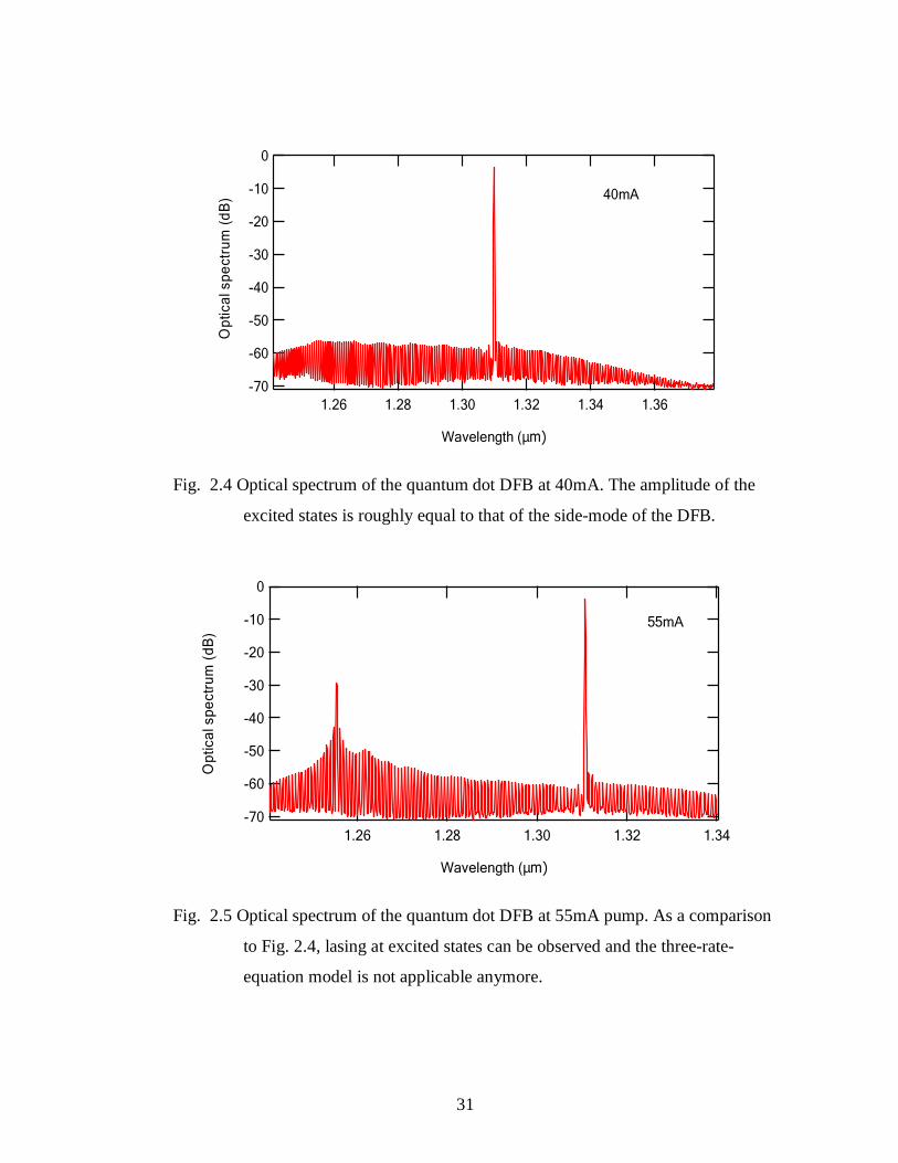
Fig. 2.4 Optical spectrum of the quantum dot DFB at 40mA. The amplitude of the
excited states is roughly equal to that of the side-mode of the DFB..........................31

xi
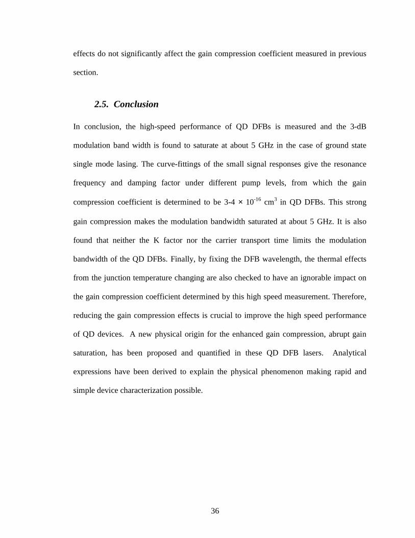
Fig. 2.5 Optical spectrum of the quantum dot DFB at 55mA pump. As a comparison to
Fig. 2.4, lasing at excited states can be observed and the three-rate-equation model is
not applicable anymore. ............................................................................................31
Fig. 2.6 Curve-fitting based on Eqn. (2.3) shows that gain compression output power Psat
is 3.7±0.4 mW...........................................................................................................32
Fig. 2.7 Curve fitting based on Eqn. (2.2) to derive the K factor and effective carrier
lifetime of the QD DFB.............................................................................................32
Fig. 2.8 The carrier transport time as a function of the pump current derived from the
small signal modulation response of the QD DFB. The error bar increases
dramatically after the excited states lasing for a pump larger than 55mA. ................33
Fig. 2.9 Effective carrier transport times, resonance frequencies and damping rates of
QD DFBs under constant junction temperature.........................................................37
Fig. 2.10 Curve-fitting of the squares of the resonance frequency to the pump current in
the QD DFB with fixed junction temperature. Gain compression is found to become
significant at a pump current of about 12-18mA, corresponding to 2.5-3.5 mW. .....37
Fig. 3.1 (a), (b) and (c) are the spectra of device A, B and C at 10 mA, respectively. (d)
is the spectrum of the commercial QW DFB at 10 mA.............................................40
Fig. 3.2 The experimental setup for the self-homodyne linewidth measurement of QD
DFBs. ........................................................................................................................41
Fig. 3.3 The self-homodyne spectra and their Lorentzian curve-fittings of QD DFB
device B at different pump levels. .............................................................................42
Fig. 3.4 The self-homodyne spectra and their Lorentzian curve-fittings of the commercial
1.3 µm QW DFB. ......................................................................................................42
Fig. 3.5 Linewidths and SMSRs of the three QD DFBs as a function of optical output
power.........................................................................................................................49
Fig. 3.6 Linewidth and SMSR of a commercial 1.3 µm QW DFB. ................................49

xii
Fig. 3.7 The figure of merit for the spectral linewidth enhancement in semiconductor
lasers nsp(1+α2) at optical gain peak as a function of the modal gain in bulk DH, QW
lasers with different number of quantum wells [101] and QD lasers with six stacks of
DWELL.....................................................................................................................50
Fig. 3.8 Schematic plot for applying an optical filter to exclude the excited-state ASE
from the self-homodyne measurement. .....................................................................51
Fig. 3.9 The measured linewidths of the QD DFB device C with different bandwidth of
the optical filter. The linewidths are found to be independent of the filter bandwidth.
..................................................................................................................................51
Fig. 4.1 Coherence collapse of a DFB laser is indicated by the dramatic broadening of
the linewidth [102]. ...................................................................................................53
Fig. 4.2 The low frequency noise of a DFB under external feedback with different
linewidth enhancement factors. Noise burst after coherence collapse is shown [102].
The α in the figure stands for linewidth enhancement factor. ...................................53
Fig. 4.3 A schematic presentation of the effects of external feedback on a semiconductor
laser. ..........................................................................................................................55
Fig. 4.4 Schematics of the experimental setup. The 2.5 Gbps pattern generator was used
only for the eye-diagram measurement. ....................................................................58
Fig. 4.5 The optical spectra of the QD LLC DFB with -14 dB and less than -60 dB
external feedback. No significant broadening is observed with the resolution of the
optical spectrum analyzer to be 0.06nm. ...................................................................60
Fig. 4.6 Spectra of the commercial QW DFB with -15 dB and less than -60 dB external
feedback. Significant broadening is observed. ..........................................................60
Fig. 4.7 Self-homodyne spectra of the QD DFB under different external feedback
strength, while linewidth re-broadening occurs at -14dB. .........................................61
Fig. 4.8 Self-homodyne spectra of the commercial QW DFB under external feedback
strength, the linewidth re-broadening at -20dB external feedback can be clearly
observed. ...................................................................................................................61
xiii
Fig. 4.9 The noise spectrum of the QD LLC DFB before coherence collapse. Low
frequency noise is the dominant component of the spectrum....................................62
Fig. 4.10 The noise spectrum of the QD LLC DFB at coherence collapse. The spikes at
integer multiples of the relaxation frequency in the noise spectrum are the indications
of the coherence collapse. .........................................................................................62
Fig. 4.11 The noise spectra of the QD LLC DFB and the QW DFB under coherence
collapse introduced by external feedback. QD LLC DFB shows a lower noise level
compared to the commercial QW DFB. ....................................................................63
Fig. 4.12. The eye-diagram of the QD DFB under 2.5 Gbps modulation with different
external feedback levels. ...........................................................................................66
Fig. 4.13. The root-of-mean-square jitter and signal-to-noise ratio (SNR) of the QD LLC
DFB and QW DFB under different external feedback ratios. Although the
degradation of the jitter is more same for the two devices, the SNR of the QD DFB
starts to degrade under -30dB external feedback, about 20 dB improvement
compared to the QW DFB.........................................................................................66
Fig. 5.1 The experimental setup for TRC measurement [116]. The QD DFB is modulated
by the pattern generator and its wavelength chirping is translated into optical
intensity variation and then recorded by the DCA.....................................................72
Fig. 5.2 A schematic drawing of the measurement of the wavelength chirping with the
optical filter built in to the OSA [116].......................................................................72
Fig. 5.3 LIV curves of the QD DFB for the TRC measurement......................................75
Fig. 5.4 The eye diagram of the output of the modulated QD DFB biased at 20 mA with
an extinction ratio of 9.5 dB. .....................................................................................76
Fig. 5.5 The chirp and corresponding power measured on the QD DFB biased at 20 mA.
The chirp at ‘0’ levels are noisier than ‘1’ levels as a result of the increased
measurement error for lower power. .........................................................................78
Fig. 5.6 TRC measurements of the chirp and power of a QW DFB as given in ref. [121].
..................................................................................................................................78

xiv
Fig. 5.7 The average chirp and the peak-to-peak modulation voltage under different DC
biases of the QD DFBs with the extinction ratio kept around 10 dB.........................80
Fig. 5.8 The shift between the center frequencies of the modulated and un-modulated
output from the QD DFB as a function of current with the extinction ratio fixed at ~
10 dB.........................................................................................................................80
Fig. 5.9 The measured effective alpha and its dependence on the output power of the QD
DFB under modulation with the extinction ratio fixed at ~ 10 dB. ...........................81
Fig. 5.10 The measured and curve-fitted chirps of the QD DFB under 15 mA, 20 mA and
35 mA DC biases with a peak-to-peak modulation voltage fixed at 250mV.............85
Fig. 5.11 The effective alpha and its dependence on the output power measured in the
QD DFB. ...................................................................................................................86
Fig. 5.12 The gain compression coefficients at different DC output powers of the QD
DFB...........................................................................................................................86
Fig. 5.13 The distortion of the gain spectrum of QD gain media due to the
inhomogeneous broadening and spectral hole burning effects. .................................87
Fig. 5.14 The overall profile of QW homogeneously-broadened gain spectrum is
clamped and kept unchanged even under a strong gain compression........................87
Fig. 5.15 The threshold gain of the QD DFB from the curve-fitting of the chirp measured
at different biases. .....................................................................................................88
Fig. 5.16 The average chirp of the QD DFB with a fixed Vpp=0.25V under different DC
current biases.............................................................................................................88

xv
LIST OF TABLES
Table 1-1. A review of some experiments on the carrier dynamics in QDs. ....................13
Table 2-1. The variation of DFB wavelength under different pumps is controlled to be
less than 0.01nm, indicating a small change of the junction temperature..................35
Table 3-1. The performance of QD DFB A, B and C and the commercial QW DFB at
room temperature. .....................................................................................................40
Table 3-2 Estimating the figure of merit for narrow linewidth in QD DFBs ...................44

1
Chapter One. INTRODUCTION
1.1. Properties of QDs: expectation and reality
It is very natural for quantum dots (QD) to become attractive after the success of
quantum well (QW) hetero-structures. The development of quantum well devices
confirms the functionality of the quantum confinement of carriers in semiconductors and
fosters the concepts and tools which are essential to design, fabricate and characterize QD
devices. Theoretically, QD lasers represent an ultimate case of the application of the size
quantization concept to semiconductor hetero-structure lasers [1].
The advantages of quantum dots compared to quantum wells stems from their unique
density of states resulted from the 3-dimensional confinement of carriers. As shown in
Fig.1.1, the energy levels of quantum dots are less convolved with each other. After the
creation of the first QD lasers in 1993 and early 1994 [2,3], various potential advantages
of QDs have been verified on actual devices, including the low transparency current [4],
increased material and differential gain [5], less temperature sensitivity [6] and reduced
linewidth enhancement factor (α parameter) [7]. Furthermore, QDs can extend the
achievable wavelengths on given substrates since the three dimensional structure of the
nanometer dots helps to relax the strain from the lattice mismatch while minimizing
dislocation formation. One of the real applications of this is the growth of 1.3 µm InAs
QD lasers on GaAs substrates. Finally, as QDs are spatially separated and the carriers are
localized once they get captured into the dots, QD gain media are more resistant to
defects than QW structures [8,9].

2
Fig. 1.1 Ideal density of states for charge carriers in structures with different dimensionalities [10].
However, quantum dots in the real world are not identical to the ideal ones people
based their predictions on. The energy barrier for carrier confinement is not finite in QDs,
first of all, indicating an imperfect confinement and the impact of continuum or unbound
states. The size and shape dispersion of QDs, which broaden the carrier distribution in k-
space, still seems insurmountable for the growth technology nowadays. Due to the large
effective mass of holes, the energy separation of holes in the strained dots is less than the
thermal energy of the typical temperature of operation. Carrier dynamics are very
different in QDs, compared to QWs, due to the insufficiency of the optical phonons with
the right energy to facilitate the carrier relaxation between energy states. All of those
realities compromise the advantages of QDs mentioned previously.
1.1.1. Gain and loss in QD media
Very low threshold current densities (26 A cm-2 in 3 stacks of dots-in-a-well
(DWELL)), very low internal losses (~ 0.5-1.5 cm-1) are found in QD lasers [4]. In a
quantum dot laser emitting at 1.16 µm, with an internal quantum efficiency of 98%, its
transparency current was measured to be 6 A/cm2 per quantum dot layer [11], compared
to 50 A/cm2 in typical QWs [12]. The maximum modal gain of the ground state is

3
measured to be 2.4 cm-1, 3.6 cm-1 and 5.7 cm-1 for a single sheet of InAs/In0.1Ga0.9As (dot
density 4x1010 cm2), InAs/In0.15Ga0.85As (dot density 3.2x1010 cm2) and InAs/In0.2Ga0.8As
(dot density 3.7x1010 cm2), respectively [13]. Although different groups reported quite
similar values of the gain, the published values of the differential gain in QDs are very
scattered, varying from 2x10-12 [14], 1.7x10⁻¹⁴ [15] to 3.1x10⁻¹⁶ cm2 [16], due in part to
the lack of agreement on the confinement factor which is related to the shape of quantum
dots and cannot be measured accurately. Since the limited number of available states in
QDs, gain will saturate, and thus the corresponding differential gain will decrease rapidly
as the carrier density approaches the dot density.
1.1.2. Temperature insensitivity
Though QD lasers demonstrated high characteristic temperature (>300K) in a
temperature range below 150-180 K [17], T0 was reported to be 120K, not much superior
compared to commercial GaAs-based QW devices, near room temperature [18]. Ideally,
the T0 value should be infinite, but the non-ideal DOS of QDs prevents this [19]. In
practice it is found to vary depending on the particular size, shape, and number of
electron and hole levels [20]. The key points for achieving improved high-temperature
operation were proposed to be large volume density, deep potential and high quantum
efficiency [21]. The T0 could also be artificially higher from the undesirable non-
radiative recombination processes in the dots or the optical confinement layer [22]. P-
type modulation doping was used to compensate for the closely spaced hole levels in
QDs and showed a T0 of about 200 K between 0 to 80 oC [19].

4
1.1.3. Linewidth enhancement factor
Typically linewidth enhancement factors are measured using the Hakki-Paoli
technique which requires a delicate control of the temperature of testing. The published
results range from negative to about 2 [23,24]. 0.1 is reported by Newell [7] in single
stack of QDs and a minimum of about 1.0 is measured by Ukhanov [16]. It is found that
the excited states and the continuum state in the QWs have severe effects on the alpha
factor of the ground state [25]. In tunneling-injection QD devices, alpha is measured to
0.15 [26] and 0.7 [15,27]. As one of its drawbacks, the Hakki-Paoli method is applicable
only under threshold and in F-P lasers. As we know, there is still no systematic study
about the alpha factor in a real QD laser operating above threshold. Gain compression
can make the alpha strongly dependent on the photon density. The above-threshold alpha
and gain compression effects will be investigated in this dissertation.
1.2. Current status of selected quantum dot devices
1.2.1. QD Amplifiers: high saturation gain, low noise, high speed, pattern effect free, XGM, XPM and four wave mixing.
QD semiconductor optical amplifiers (SOAs) are among the best successful applications
of QDs and have been exposed to a thorough investigation. It is instructive to review the
QD SOA research to help understand some of the results described for DFB lasers later in
this dissertation. Although QDs have a smaller modal gain than QWs due to a smaller
physical volume, or smaller confinement factor, a longer waveguide can generally result
in more available gain as long as the gain is not significantly saturated. Therefore, the
most fundamental issue in a SOA is the gain saturation power which sets a limit on the
maximum extractable power out of the SOA [28]. The physics of this gain saturation here

5
is due to the competition between the carrier recombination time and the stimulated
emission time, as a result of the steady state solution of rate equations. It is notable here
that this gain saturation is different from the gain compression effect resultant from the
competition between the carrier equilibrium time and the stimulated emission time as
indicated by the steady state solution of master equations. Since the gain saturation power
is inversely proportional to the differential gain, which gets saturated much easier in QDs
than QWs, it is expected that QDs will have a very high gain saturation power [29,30].
Experimentally, a gain-saturation power over 20 dBm is achieved in QD SOAs [31].
High amplification (>18 dB) of 200-fs pulses was achieved in a quantum-dot (QD)
semiconductor amplifier over a spectral range exceeding 100nm without pulse distortion
[32]. The noise of an SOA is from the spontaneous emissions and the figure of merit is
the noise figure, defined as the degradation of the input and output signal to noise ratio. It
is well known that the noise figure is proportional to the population inversion factor, nsp,
which is believed to be smaller in QDs due to the abrupt density of states [30]. A noise
figure of 5 dB is demonstrated in QD SOAs [33]. One of the most significant features of
QD SOAs is the high-speed performance. In typical bulk or QW SOAs, the whole gain
spectrum is typically within the gain homogeneous broadening width. Therefore, the
carriers will respond as a whole unit and carrier recombination lifetime will determine the
high-speed performance. In QDs, however, the homogenous broadening is found to be
narrower than the inhomogeneous one and significant spectral hole burning can be
observed. In this case, only the carriers within the narrower homogeneous broadening
respond as a whole unit and the carriers outside of this homogeneous broadening act as a
reservoir [34,35]. This physical phenomenon has relevance to the operation of QD lasers

6
as well and will be discussed later in the thesis. For the QD SOA, the outcome is that the
carrier dynamics are determined by the carrier equilibrium time (1~10 ps), instead of the
carrier recombination time (~1 ns). In this sense, QDs are much faster gain media than
QWs. Experimentally, people have shown that the pattern effect is much weaker in QD
SOAs than QW SOAs [36-39]. This ultrafast response is also proven in cross gain
modulation due to the same carrier dynamics [40-42]. No experiments about cross phase
modulation have been reported by now in QDs.
Four wave mixing has been studied by different groups in quantum dot amplifiers
[36,41,43-46]. FWM is a well-established technique to characterize the carrier dynamics.
The efficiency of FWM in QDs, which is proportional to χ(3)/g (g is gain) in QDs is found
comparable to QWs, not enhanced by the three-dimensional confinement as theoretically
predicted [47], probably due to the non-ideal features of the QD medium. Appendix 2
discusses in the FWM in QD DFB lasers.
1.2.2. FP lasers: High power and filamentation free
Besides the low threshold, high efficiency and temperature insensitivity mentioned
previously, high power is demonstrated in QD devices. GaAs-based QD-lasers emitting
at 1.3 µm exhibit output power of 5 W and single transverse mode operation up to
300mW. An output power of 5 W has been obtained in 1.5 µm QD lasers. Furthermore,
single-mode lasers at 1.16 µm and 1.3 µm show no beam filamentation and a reduced M2,
which is believed to be related to the low linewidth enhancement factor [48].

7
1.2.3. External cavity tunable lasers: wide tunable range and low threshold
A grating-coupled external-cavity quantum dot laser is tuned across a 201 nm range
around 1200 nm at a maximum bias of 2.87 kA/cm2, one order of magnitude less than the
bias required for comparable tuning of quantum well lasers [49]. Tuning range from
1.095 to 1.245 µm, extended from the energy levels of the ground state to excited states,
is achieved in QD external tunable lasers with a threshold density less than 1.1 kA/cm2 at
any wavelength. This large tunable range and low threshold are the product of the rapid
carrier filling of the higher energy states under a low pumping current and homogeneous
broadening in the QD ensemble [50].
1.2.4. QD Mode-locked lasers: ps pulse generation
Intuitively, the broad spectrum in QD gain media indicates a narrow pulse from QD
mode-locked lasers. The low spontaneous emission noise as discussed in previous
sections also suggests low amplitude and frequency noise in QD pulse sources. More
importantly, the absorption in quantum dots is more easily saturated than in QWs.
Passive mode locking was achieved at 1.3 µm in oxide-confined, two-section, bistable
quantum dot (QD) lasers with an integrated intra-cavity QD saturable absorber [51]. One
of the sections is forward biased to provide gain, while the other one reversed biased as a
saturable absorber. Fully mode-locked pulses at a repetition rate of 7.4 GHz with a
pulsewidth of 17 ps were observed without self-pulsation.
8
1.2.5. Distributed feedback lasers (DFB): Threshold, efficiency, SMSR, temperature performance, high speed performances, linewidth, feedback resistance and chirp
Single mode lasers with sufficient output power are fundamental building blocks for
optical communication systems. InAs/GaAs QD DFBs are fabricated mainly with a loss-
coupled grating deposited laterally to the ridge waveguide. No index-coupled InAs/GaAs
QD DFBs are reported by now. In 1999 Kamp [52] et. al. reported complex coupled
distributed feedback lasers at 980nm based on a single layer of InGaAs/GaAs self-
organized quantum dots grown by molecular beam epitaxy. A threshold current of 14 mA,
differential efficiency of 0.33 W/A and a side-mode suppression ratio (SMSR) of > 50 dB
have been obtained in these devices. Single mode operation was observed for
temperatures from 20 to 213 oC. In 2001, Klopf achieved single-mode operation of 1.3
m InAs/GaInAs QD DFBs with a SMSR of up to 55dB, threshold currents as low as
17mA and CW output powers of up to 8mW at room temperature [53]. The InAs/GaAs
QD DFBs studied in this dissertation are provided by Zia Laser, InC. More than 5 GHz
small-signal modulation bandwidth was observed in these first devices indicating the
potential for high-speed operation of quantum dot lasers [54,55]. The linewidth-power
product of the QD DFBs is measured to be 1.2 MHz-mW, one order of magnitude lower
that the typical value of QW DFBs [56]. The same QD devices shows an improvement of
external feedback resistance: 8 dB on the critical coherence collapse feedback level and
20 dB in term of signal-to-noise degradation [57]. These devices will be discussed in
detail in this dissertation.

9
1.3. Carrier dynamics in QDs
It has been controversial for a long time whether QDs are a fast or slow gain media. This
is a fundamental question for applications such as high-speed light sources, high-speed
amplifiers, all-optical gates and switches using QDs. It was proposed that the carrier
relaxation between different levels could be hindered due to the lack of phonons with the
large energy corresponding to the level spacing in QDs, the so called “phonon
bottleneck” [58-63]. The phonon bottleneck is observed in quantum dots occupied with
just one electron without a hole, and without a population in the wetting layer [64].
Meanwhile, recent proposals invoke fast mechanisms other than the phonon-assisted
process in QDs, such as, electron-hole scattering [65], Auger process [66,67], phonon
spectrum broadening by the QD itself [68], and support fast carrier dynamics in QDs.
The carrier dynamics is characterized by three parameters: dephasing time, electron
relaxation time and hole relaxation time. The dephasing time, T2, is basically the time
scale within which the carrier is coherent to itself. Since T2 is inversely proportional to
the homogenous linewidth, it can be the intrinsic limit of the -function of the DOS in
QDs. The electron and hole relaxation times (measured as recovery times in pump-probe
experiments), e and τh,, are the time constants for electrons and holes to reach their intra-
band equilibrium. Measurements of carrier dynamics have been carried out on QD
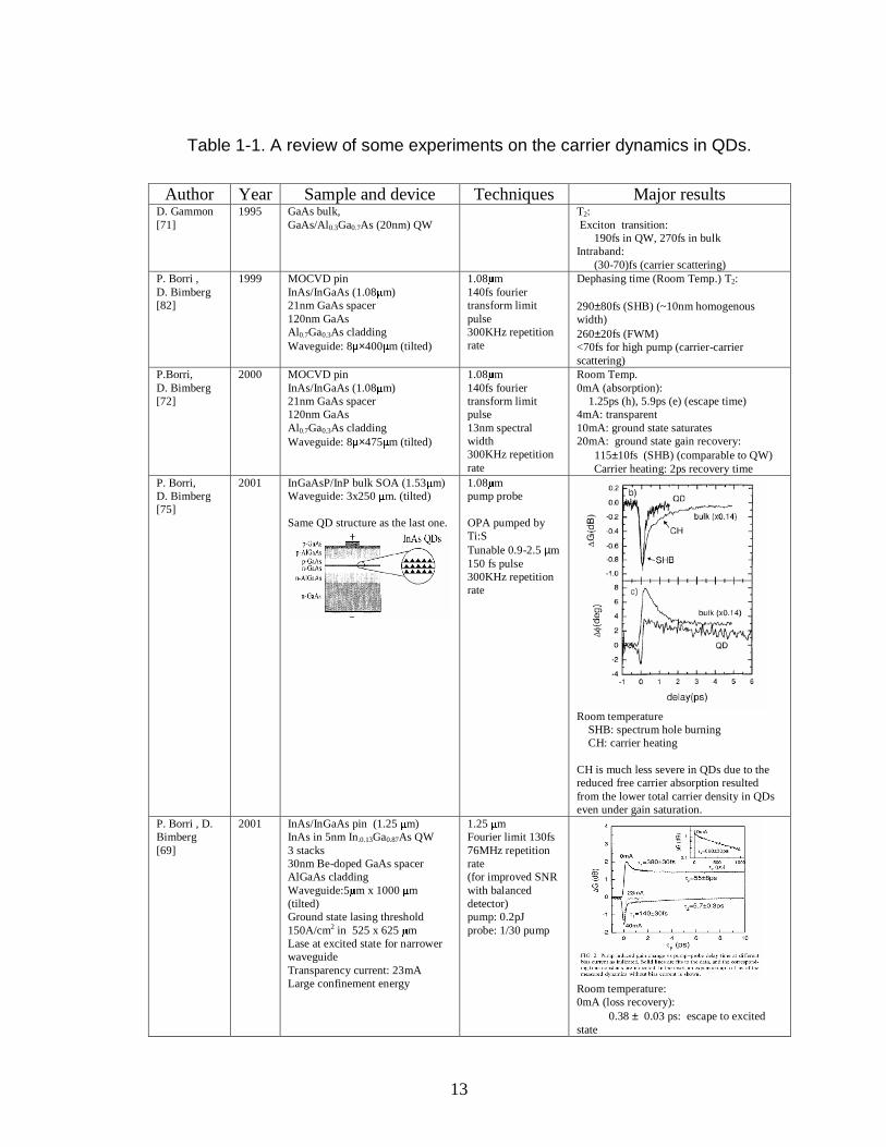
materials from different groups as listed in Table.1. The results vary broadly due to the
structural difference of the QD samples. T2 was measured to be about 150 fs (~9 nm
homogeneous broadening width) in 1.25 m MOCVD-grown QDs under normal
operating conditions of lasers at room temperature [69] . This result is consistent with the
spectral width 13 nm (10.5 meV) of homogeneous broadening derived from the gain

10
behavior of the 1.23 µm DWELL tunable laser built at CHTM with an external cavity
[70]. Since T2 in QWs is about 30-50 fs for the intra-band transitions [71] , it suggests
that the width of homogeneous broadening of QDs will be about 3 times narrower than
that of QWs. The explanation could be that once the carriers get relaxed into the QDs,
they are localized and the energy barrier reduces their chance to be scattered by phonons
and carriers, a similar mechanism underlying the fact that the excitonic transition
generally has a longer dephasing time than the intra-band one [71].
For the carrier relaxation or capture time in the QDs, Table.1 shows that the carrier-
carrier scattering provides a fast intradot relaxation on the order of 0.1-1 ps [47,69,72,73]
while the carrier capture from the surrounding QWs into QDs by phonon scattering takes
about 1-10 ps [33,47,69,73,74]. The phonon bottleneck with a time constant of 950 ps is
observed only at low temperature ( < 40 K ) and low pump level ( less than one e-h pair
per dot) [64]. From the loss recovery pump-probe experiments, the escape time constant
of the holes in QDs is measured to be 1.25 ps, faster than the 5.9 ps of the electrons [72].
The recombination lifetime of the carriers in QDs are found to be 140 ps[33], 660 ps [69]
and 900 ps [74]. The carrier heating is found not to be severe in the only study of its kind,
resulting from the low total carrier density in 1.0 µm QDs even under gain saturation [75].
The data given in Table 1.1 are quite scattered due to the differences between the material,
structure, barrier height and measurement technique of the experiments. The details of
those experiments are given in Table. 1.1.
As a conclusion, the phonon bottleneck is not present in the devices under room
temperature or high pump, which is the case of most interest for semiconductor lasers.
However, even though the carrier-carrier scattering can improve part of the capture time,
11
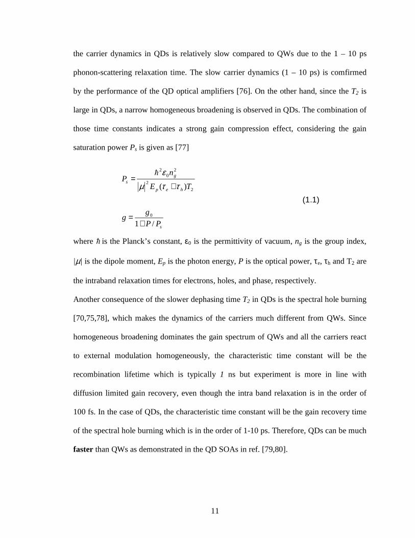
the carrier dynamics in QDs is relatively slow compared to QWs due to the 1 – 10 ps
phonon-scattering relaxation time. The slow carrier dynamics (1 – 10 ps) is comfirmed
by the performance of the QD optical amplifiers [76]. On the other hand, since the T2 is
large in QDs, a narrow homogeneous broadening is observed in QDs. The combination of
those time constants indicates a strong gain compression effect, considering the gain
saturation power Ps is given as [77]
s
hep
gs
PP
gg
TE
nP
/1
)(
0
2
2
20
2
+=
+=
ττµε
(1.1)
where is the Planck’s constant, ε0 is the permittivity of vacuum, ng is the group index,
|µ| is the dipole moment, Ep is the photon energy, P is the optical power, τe, τh and T2 are
the intraband relaxation times for electrons, holes, and phase, respectively.
Another consequence of the slower dephasing time T2 in QDs is the spectral hole burning
[70,75,78], which makes the dynamics of the carriers much different from QWs. Since
homogeneous broadening dominates the gain spectrum of QWs and all the carriers react
to external modulation homogeneously, the characteristic time constant will be the
recombination lifetime which is typically 1 ns but experiment is more in line with
diffusion limited gain recovery, even though the intra band relaxation is in the order of
100 fs. In the case of QDs, the characteristic time constant will be the gain recovery time
of the spectral hole burning which is in the order of 1-10 ps. Therefore, QDs can be much
faster than QWs as demonstrated in the QD SOAs in ref. [79,80].

12
The strong gain compression and spectral hole burning also introduces interesting
behavior in the linewidth enhancement factor. The gain compression itself can increase
the effective alpha by
)/1(0 seff PP+= αα (1.2)
At the same time, since the gain at the lasing wavelength is clamped in a laser above
threshold, the spectrum hole burning will result in an increase of the carrier density on the
energy levels outside of the spectrum hole burned around the lasing wavelength,
especially the excited states, which in turn further increases the alpha factor [81]. This
effect becomes more severe if the ground state gain is close to being saturated with the
carrier density. Investigating these effects in QD DFB lasers is one of the major subjects
of this dissertation.
13
Table 1-1. A review of some experiments on the carrier dynamics in QDs.
Author Year Sample and device Techniques Major results D. Gammon [71]
1995 GaAs bulk, GaAs/Al0.3Ga0.7As (20nm) QW
T2: Exciton transition:
190fs in QW, 270fs in bulk Intraband:
(30-70)fs (carrier scattering) P. Borri , D. Bimberg [82]
1999 MOCVD pin InAs/InGaAs (1.08 m) 21nm GaAs spacer 120nm GaAs Al 0.7Ga0.3As cladding Waveguide: 8 ×400 m (tilted)
1.08 m 140fs fourier transform limit pulse 300KHz repetition rate
Dephasing time (Room Temp.) T2: 290±80fs (SHB) (~10nm homogenous width) 260±20fs (FWM) <70fs for high pump (carrier-carrier scattering)
P.Borri, D. Bimberg [72]
2000 MOCVD pin InAs/InGaAs (1.08 m) 21nm GaAs spacer 120nm GaAs Al 0.7Ga0.3As cladding Waveguide: 8 ×475 m (tilted)
1.08 m 140fs fourier transform limit pulse 13nm spectral width 300KHz repetition rate
Room Temp. 0mA (absorption): 1.25ps (h), 5.9ps (e) (escape time) 4mA: transparent 10mA: ground state saturates 20mA: ground state gain recovery: 115±10fs (SHB) (comparable to QW)
Carrier heating: 2ps recovery time P. Borri, D. Bimberg [75]
2001 InGaAsP/InP bulk SOA (1.53 m) Waveguide: 3x250 m. (tilted) Same QD structure as the last one.
1.08 m pump probe OPA pumped by Ti:S Tunable 0.9-2.5 µm 150 fs pulse 300KHz repetition rate
Room temperature
SHB: spectrum hole burning CH: carrier heating
CH is much less severe in QDs due to the reduced free carrier absorption resulted from the lower total carrier density in QDs even under gain saturation.
P. Borri , D. Bimberg [69]
2001 InAs/InGaAs pin (1.25 m) InAs in 5nm In.0.13Ga0.87As QW 3 stacks 30nm Be-doped GaAs spacer AlGaAs cladding Waveguide:5 m x 1000 m (tilted) Ground state lasing threshold 150A/cm2 in 525 x 625 m Lase at excited state for narrower waveguide Transparency current: 23mA Large confinement energy
1.25 m Fourier limit 130fs 76MHz repetition rate (for improved SNR with balanced detector) pump: 0.2pJ probe: 1/30 pump
Room temperature: 0mA (loss recovery): 0.38 ± 0.03 ps: escape to excited state

14
55 ± 8 ps : escape to the wetting layer 0.66 ns : recombination lifetime T2 : 220 ± 10 fs 40mA (gain recovery):
0.14 ± 0.03 ps: carrier-carrier scattering
(faster than undoped GaAs spacer) 5.7 ± 0.3 ps: phonon-assisted relaxation
T2 : 150 ± 10 fs
K. Kim, P. Bhattacharya [73]
2002 MBE In0.4Ga0.6As (QD 975nm) Four stacks 2.5nm GaAs barrier 100nm GaAs wetting layer 500nm AlGaAs carrier confiment grown at 520oC, other 620oC dot size: height 7nm, base 14nm dot density: 5 x 1010 cm-2 MBE InAs (QD 1000nm) 2nm GaAs barrier Five stacks
85fs 3.5 J 250KHz pump: 10nm bandwidth filter of the Ti: Sapphire white light source 14ps delay with respect to the gain pulse Optically injection by 800nm gain pulse
Measurement T=8-15K Slightly higher at room temp. Burn a hole in ground state first, after ~130ps hole in excited state occurs and get localized In0.4Ga0.6As: 0.13ps intradot carrier-carrier scattering 1ps carrier capture into dot InAs 0.18ps intradot carrier-carrier scattering 1.8ps carrier capture into dot Less than one pair per dot: 5.2ps for electrons 0.6ps for holes
J. Urayama, P. Bhattacharya [64]
2001 MBE In0.4Ga0.6As (QD 975nm) Same as the last one
100fs 250KHz 10nm filtering
T= 40KHz pump with less than one e-h pair per dot. For excited state: Relax to ground state τ21=7ps Capture from barrier: geminate 2.5 ps Nongeminate 8.5 ps Bottleneck time constant: 750ps For ground state: Capture from barrier: geminate 30ps Nongeminate 100ps
15
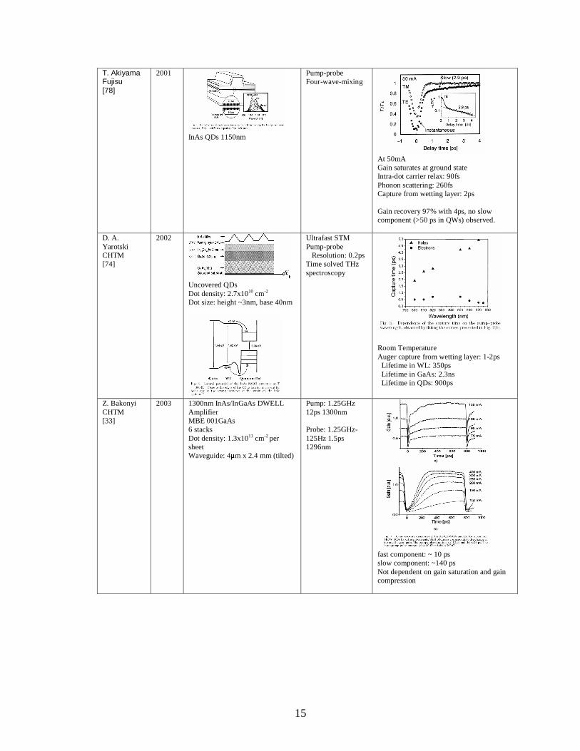
T. Akiyama Fujisu [78]
2001
InAs QDs 1150nm
Pump-probe Four-wave-mixing
At 50mA Gain saturates at ground state Intra-dot carrier relax: 90fs Phonon scattering: 260fs Capture from wetting layer: 2ps Gain recovery 97% with 4ps, no slow component (>50 ps in QWs) observed.
D. A. Yarotski CHTM [74]
2002
Uncovered QDs Dot density: 2.7x1010 cm-2 Dot size: height ~3nm, base 40nm
Ultrafast STM Pump-probe Resolution: 0.2ps Time solved THz spectroscopy
Room Temperature Auger capture from wetting layer: 1-2ps Lifetime in WL: 350ps Lifetime in GaAs: 2.3ns Lifetime in QDs: 900ps
Z. Bakonyi CHTM [33]
2003 1300nm InAs/InGaAs DWELL Amplifier MBE 001GaAs 6 stacks Dot density: 1.3x1011 cm-2
per sheet Waveguide: 4 m x 2.4 mm (tilted)
Pump: 1.25GHz 12ps 1300nm Probe: 1.25GHz-125Hz 1.5ps 1296nm
fast component: ~ 10 ps slow component: ~140 ps Not dependent on gain saturation and gain compression

16
1.4. Motivation for this dissertation
As shown in previous reviews, much research has been done in QD devices. However,
the dynamic properties of the QD DFBs have not been systematically studied, including
the high-speed performance, linewidth, external feedback effects and wavelength
chirping. The advantage of QD DFB, compared to QD FP lasers, is the single mode
operation that makes the photon-carrier interaction better fitted to the standard rate
equations and easier to study. From the physics point of view, the motivation of this
dissertation is to investigate the effects of the increasing optical power on the basic
parameters of the devices. For example, as the linewidth enhancement factor (or alpha
parameter) is measured mostly under threshold, it is important to understand how the
alpha factor behaves above threshold. Gain compression, which is expected to be strong
in QD devices as discussed in Section 1.2, will also be characterized in this dissertation
by the dynamics of QD DFBs.
The remaining part of this chapter will be a general discussion of the fabricated QD
DFBs, including their material design, light-current (LI) curves, optical spectrum, and
temperature performance.
Chapter 2 will be devoted to the high speed performance of QD DFBs. The
modulation bandwidth, bandwidth saturation, limiting factors and gain compression
effects are investigated in QD DFBs.
Chapter 3 will focus on the static linewidth issue in QD DFBs. Narrow linewidth is
demonstrated, while the linewidth re-broadening is observed at low photon density,
suggesting a strong gain compression. The effect of gain offset, defined as the spectral
distance between the DFB lasing mode and the peak of ground state gain, is presented.

17
Suggestions for narrow linewidth QD devices are given after analyzing the experimental
data.
Chapter 4 will present the experiments investigating the external feedback resistance
of QD DFBs by studies on the effects of external feedback on optical spectra, LI curves,
CW linewidth, CW intensity noise, and the signal-to-noise ratio (SNR) and jitter under
2.5 Gbps modulation. A significant improvement in the external feedback will be
demonstrated with a discussion about the factors determining the external feedback
resistance.
Chapter 5 will investigate the frequency chirp of the QD DFBs under large-signal
modulation, simulating the operation condition in a real communication system. Time-
resolved chirp measurement is carried out and the experimental result will be discussed.
The wavelength chirping of the QD DFB under external modulation will be measured.
The dependence of alpha parameter on the photon density in the devices will be
characterized and the gain compression coefficient will be determined.
The last chapter will summarize this dissertation and make some suggestion for future
work on QD devices.
In Appendix one, the effects of the gain saturation with the carrier density on the
dynamic properties of QD DFBs will be modeled, include the limitation on the
modulation bandwidth and the dependence of alpha parameter on the output power of the
QD devices.
In Appendix two, the four wave mixing effects in QD DFBs will be discussed.
Wavelength conversion is demonstrated with an efficiency from -15dB to -30dB for a
spectral detuning from 0.33nm to 8nm. The cavity resonance effect is also characterized.
18
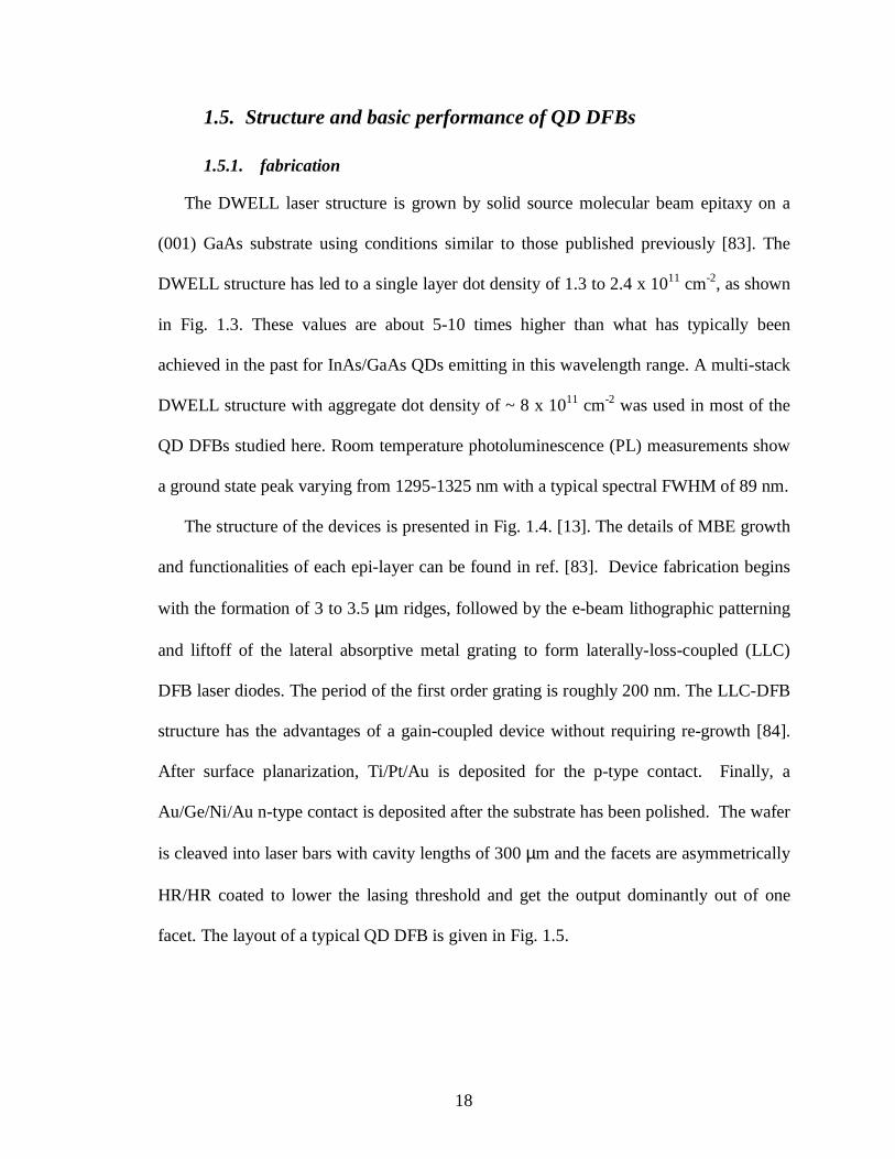
1.5. Structure and basic performance of QD DFBs
1.5.1. fabrication
The DWELL laser structure is grown by solid source molecular beam epitaxy on a
(001) GaAs substrate using conditions similar to those published previously [83]. The
DWELL structure has led to a single layer dot density of 1.3 to 2.4 x 1011 cm-2, as shown
in Fig. 1.3. These values are about 5-10 times higher than what has typically been
achieved in the past for InAs/GaAs QDs emitting in this wavelength range. A multi-stack
DWELL structure with aggregate dot density of ~ 8 x 1011 cm-2 was used in most of the
QD DFBs studied here. Room temperature photoluminescence (PL) measurements show
a ground state peak varying from 1295-1325 nm with a typical spectral FWHM of 89 nm.
The structure of the devices is presented in Fig. 1.4. [13]. The details of MBE growth
and functionalities of each epi-layer can be found in ref. [83]. Device fabrication begins
with the formation of 3 to 3.5 µm ridges, followed by the e-beam lithographic patterning
and liftoff of the lateral absorptive metal grating to form laterally-loss-coupled (LLC)
DFB laser diodes. The period of the first order grating is roughly 200 nm. The LLC-DFB
structure has the advantages of a gain-coupled device without requiring re-growth [84].
After surface planarization, Ti/Pt/Au is deposited for the p-type contact. Finally, a
Au/Ge/Ni/Au n-type contact is deposited after the substrate has been polished. The wafer
is cleaved into laser bars with cavity lengths of 300 µm and the facets are asymmetrically
HR/HR coated to lower the lasing threshold and get the output dominantly out of one
facet. The layout of a typical QD DFB is given in Fig. 1.5.

19
1.5.2. Optical spectra
The DFB lasers emitted single-mode with SMSR of greater than 50 dB in a
wavelength range from 1295-1328 nm, depending on the grating period. Fig. 1.6 shows
the typical optical spectra of the QD DFBs. Although no pure stop band is observed, a
side-mode about 4nm away presents might rise from the residual index-coupling of the
metal grating. As the pump increases up to about 10-17 times of the threshold, depending
on different devices, the excited states about 60 nm away from the ground state start to
lase limiting the single-mode to this pumping level. This result indicates that the total
carrier density is not clamped above threshold, which can be explained by the narrow
width (~20 nm) of the homogeneous broadening and slow carrier relaxation time in QDs
discussed in Chapter 1.
1.5.3. LIV and temperature performance
The typical threshold of QD LLC DFBs is less than 5mA with a slope efficiency of
about 12-17%, while the FP lasers fabricated on the same wafer show a lower threshold
and a slope efficiency about 25%. The turn-on voltage is 1.1 Volt. As shown in Fig. 1.7,
the turn-on is not abrupt and further reduction or modified grading of junction barriers in
the device will improve the carrier injection.
The detailed study of the temperature performance of those QD DFBs can be found in
ref. [55]. The temperature shift of the DFB mode is 0.1 nm/K, determined by the thermal
effect on the refractive index in GaAs-based materials. The gain peak of QDs is found to
shift at a rate of 0.25 nm/K, compared to the value of 0.4 nm/K of QWs. Therefore, QD
DFBs are shown to have a wider range of temperature operation [52]. The temperature
performance of the DFBs depends on the sign and amplitude of the gain offset: whether

20
the gain peak is moving toward or away from the DFB mode. In a negative gain offset
device (the DFB mode on the shorter wavelength side relative to the gain peak), T0 is
found to be around 50K, while in a position gain offset, for a low pump level, threshold is
independent of the ambient temperature as shown in Fig. 1.7 and Fig. 1.8.

21
Fig. 1.2 Atomic force micrograph image of the InAs DWELL active region showing
an average 1.3x1011 cm-2 single-layer dot density.
Fig. 1.3 A typical QWELL laser structure. 2.4 ML of InAs is deposited into a 10nm
width InGaAs well for dot formation. The quantum dot and well are grown
at 590 oC while the other layers at 610 oC. For multi-stack structures, GaAs
spacers of 10-40nm width are deposited between the QWELL layers. Data
and figure is from Ref. [13]

22
Fig. 1.4 The structure of a typical QD DFB.

23
!" ## $
Fig. 1.5 A typical optical spectrum of QD DFBs.
%#
&'
($
(
Fig. 1.6 LIV curves of a QD DFB shows a threshold of 3mA, a slope efficiency
about 17% and a turn-on voltage of 1.1 V.

24
Fig. 1.7 Temperature performance of a QD DFB with a gain offset about -8.4 nm
[55].
Fig. 1.8 The LI characteristics at various temperatures for a DFB laser with a gain-
offset of 8.5nm [55].
0
2
4
6
8
0 10 20 30 40 50Current (mA)
Pow
er (m
W)
10oC
30oC
80oC
100oC
50oC
0
2
4
6
8
0 10 20 30 40 50Current (mA)
Pow
er (m
W)
10oC30oC
80oC
100oC
50oC

25
Chapter Two. HIGH SPEED PERFORMANCE OF QD
DFBS
2.1. Introduction
High-speed semiconductor lasers are compact, reliable and inexpensive coherent
sources for high-bit-rate optical communication systems. Among all the properties of
high speed lasers, modulation bandwidth is the most important one. Efforts have been put
on QD devices to improve the high speed performance, especially since the lasing
wavelength of QDs on GaAs covers 1.3 m, the zero-dispersion window of commercial
communication systems. By now, however, most of the high speed performance is
measured in QD FPs [85,86]. The high speed performance of QD DFBs was reported
very briefly in ref. [54] without giving physical analyses. A systematical study of the high
speed performance of QD DFBs will be presented in this chapter.
The advantages of using QD DFBs, rather than FPs, to study high-speed properties
are obvious. First of all, DFBs are more directly related to the real applications in
communication systems. Secondly, the single mode of DFBs eliminates the effect of
multimode dynamics of FPs, including mode hopping and mode competition under
external modulation. Finally, since the DFB wavelength is associated with the junction
temperature of the device, it can be fixed at a certain value by adjusting the heat sink
temperature so that the thermal effects will be reduced and even eliminated in this high-
speed measurement.

26
The high-speed performance of semiconductor lasers is typically characterized by their
response to external small-signal modulation. Since the amplitude of the external
modulation is small, the consequential optical response can be linearly tracked back to
the driving force, that is, the modulation on the current injection. In dots-in-a-well QD
structures, the carriers are injected into the QW first and then relax into the QDs. The
slow relaxation corresponds to the slow carrier transport from the QW into the ‘active’
levels and can limit the high-speed performance as a parasitic RC constant. Based on this
simplification, the dynamics of QD lasers can be described by a similar set of equations
applied to SCH QW lasers considering the carrier transport from the SCH to QWs [87].
There are three rate equations in this model: one for the carriers directly involved in the
lasing process, one for the carriers functioning as a reservoir outside of the lasing
wavelength and another one for the photon density inside the laser cavity. By this model,
the optical modulation response M(f) of a QD laser is given as [85]:
))2(1)()((
1)(
222222
2
cr fffffM
τπγ ++−∝ (2.1)
The relationship between the resonance frequency fr and the damping factor defines the
K-factors as:
effrKf
τγ 12 += (2.2)
)1(
)( 02
S
SaV
sp
gR ετ
χω
+≈ (2.3)
sat
th
sat
ps
I
IIg
P
Pg
P
g
S
gg
−+
≡+
≡+
≡+
=1111
0000
εε (2.4)

27
where τc is the carrier transport time which includes capture, eff is the effective carrier lifetime, Vg is the
group velocity, a0 the differential gain without gain compression, S the photon density, P is the output
power measured at the facet of the device, I the pump current, Ith is the threshold current, p is the photon
lifetime, χ=1+τesc/τc is the modification factor due to the carrier transport with τc the carrier capture time
and τesc the carrier escape time, s and p are the gain compression coefficients related to photon density and
output power respectively. The introduction of Psat and Isat is for the convenience to estimate at what output
power or DC pump current the gain compression becomes significant. The gain compression factor, s, can
be calculated using Eqn. (2.3) if ωR and S can be experimentally obtained. The K factor will give us the
ultimate limit of the 3-dB modulation bandwidth, which is 8.89/K. The carrier transport time, τc, gives rise
to the parasitic-like low frequency roll-off in Eqn. (2.1). The τc must be extended to include various
parasitic effects, such as the equivalent RC constants of the p-n junction and the measurement circuit, since
they are indistinguishable from the transport effect.
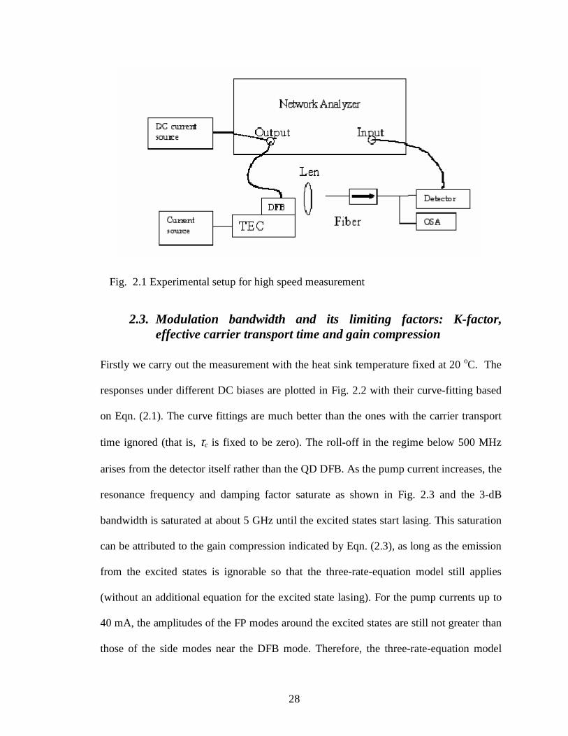
2.2. Experimental setup
The experimental setup is presented in Fig.2.1. The high-speed performance was
measured using a HP8722D network analyzer and a New Focus 1014 detector with a
bandwidth of 25GHz. An optical isolator is used to avoid external feedback into the
device. The heat sink temperature is fixed during the first part of the measurements. In
the second part of the experiment, as a comparison, the DFB wavelength is fixed to
isolate the thermal effects inherent in the first part.
28
Fig. 2.1 Experimental setup for high speed measurement
2.3. Modulation bandwidth and its limiting factors: K-factor, effective carrier transport time and gain compression
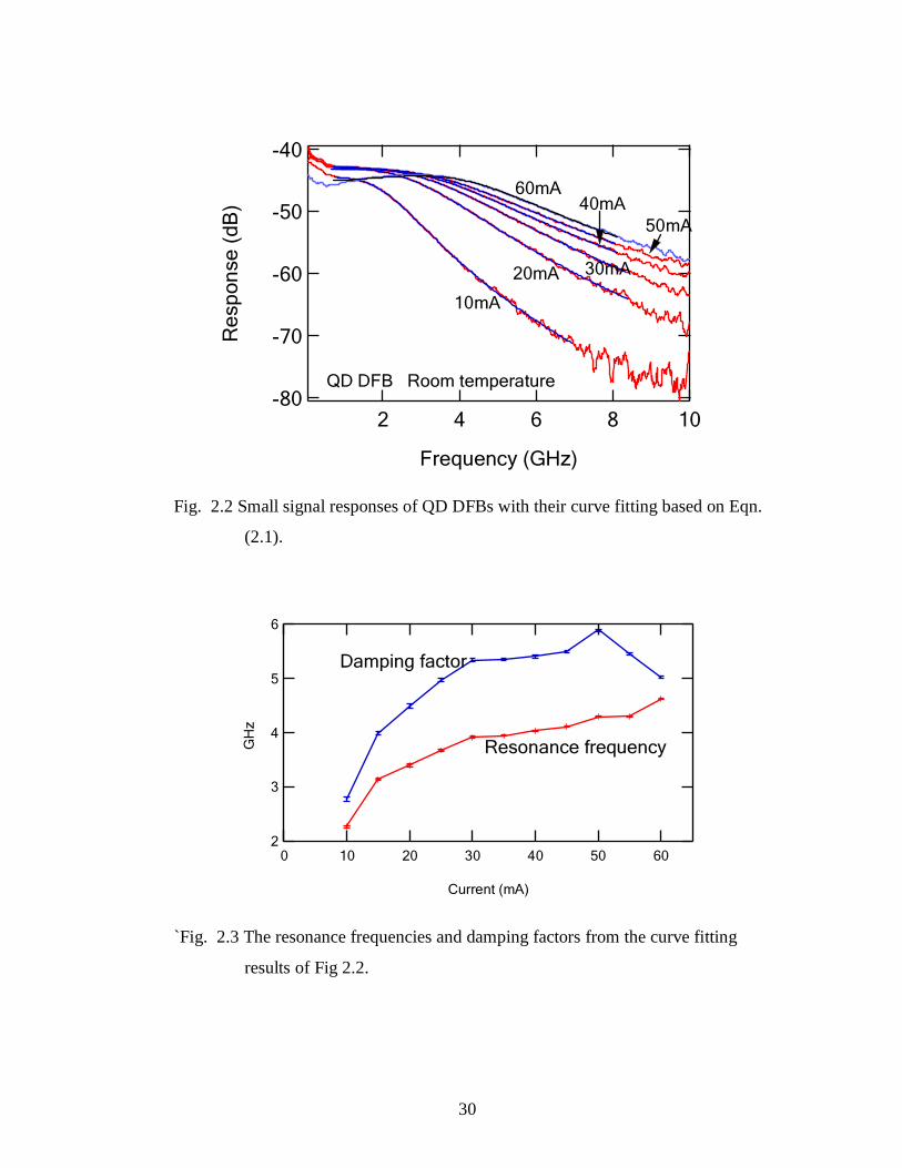
Firstly we carry out the measurement with the heat sink temperature fixed at 20 oC. The
responses under different DC biases are plotted in Fig. 2.2 with their curve-fitting based
on Eqn. (2.1). The curve fittings are much better than the ones with the carrier transport
time ignored (that is, τc is fixed to be zero). The roll-off in the regime below 500 MHz
arises from the detector itself rather than the QD DFB. As the pump current increases, the
resonance frequency and damping factor saturate as shown in Fig. 2.3 and the 3-dB
bandwidth is saturated at about 5 GHz until the excited states start lasing. This saturation
can be attributed to the gain compression indicated by Eqn. (2.3), as long as the emission
from the excited states is ignorable so that the three-rate-equation model still applies
(without an additional equation for the excited state lasing). For the pump currents up to
40 mA, the amplitudes of the FP modes around the excited states are still not greater than
those of the side modes near the DFB mode. Therefore, the three-rate-equation model

29
should apply up to at least 40 mA. The optical spectrum at 40 mA is shown in Fig. 2.4
compared to the case of excited-state lasing at 55 mA as illustrated in Fig. 2.5.
In Fig. 2.6, we curve-fit the square of the resonance frequency as a function of output
power and find that the characteristic output power for gain compression, Psat, is 3.7±0.4
mW. The definition of Psat is given in Eqn. (2.4). With this value of the gain compression
factor, the maximum resonance frequency is estimated to be 4.9 GHz. The curve fitting
range can be extended up to 50 mA (still below the threshold of excited-state lasing) as
shown in Fig. 2.6, confirming that the applicability of the rate equation model without
considering the excited state lasing.
Given the facet reflectivity and modal volume of the DFB laser, we can calculate the gain
compression coefficient, s, to be 3-4×10-16 cm3, which is more than 30 times higher than
the typical value of QWs and is consistent with the value of 4×10-16 cm3 measured by D.
Bimberg et. al. in QD FPs with the same technique [86]. A modified nonlinear gain
coefficient expression has been derived to explain this large enhancement of εs in QD
lasers. The novel theory is detailed in Appendix 1. The important result is
sth
effs gg
g εε−
=max
max, (2.5)
with gmax the maximum gain supplied by the QD active region, gth the threshold gain and
εs_eff the effective gain compression factor. This enhancement is unique to QD lasers due
to the abrupt gain saturation with carrier density. In these particular DFB lasers, gmax is
estimated to be 15 cm-1 and gth is about 12 cm-1. This makes the enhancement factor
gmax/(gmax-gth) about 5.
30
)#$#
*+,-./
'
' '
'
'
011*)$$
'
Fig. 2.2 Small signal responses of QD DFBs with their curve fitting based on Eqn.
(2.1).
-./
&'
1 2$
)#$2+,
`Fig. 2.3 The resonance frequencies and damping factors from the curve fitting
results of Fig 2.2.
31
#
333333
µ
'
Fig. 2.4 Optical spectrum of the quantum dot DFB at 40mA. The amplitude of the
excited states is roughly equal to that of the side-mode of the DFB.
#
33333
µ
'
Fig. 2.5 Optical spectrum of the quantum dot DFB at 55mA pump. As a comparison
to Fig. 2.4, lasing at excited states can be observed and the three-rate-
equation model is not applicable anymore.

32
)#$*+,-./
$4
2"56"78"79
53:3-./
953:3
;" Ω
!" ##
Fig. 2.6 Curve-fitting based on Eqn. (2.3) shows that gain compression output power
Psat is 3.7±0.4 mW.
1 2$
γ
Ω
!" ##
7τ
Fig. 2.7 Curve fitting based on Eqn. (2.2) to derive the K factor and effective carrier
lifetime of the QD DFB.

33
The damping factor is plotted in Fig. 2.7 as a function of the square of resonance
frequency. Curve fitting based on Eqn. 2.2 shows a K factor of 0.23 GHz-1 and an
effective carrier lifetime of 590 ps. It is notable that the linearity can be extended to 50
mA pump, suggesting that the three-rate-equation model applies as long as no lasing
occurs at the excited states. When the pump is greater than 55 mA, the excited-states
start to lase, and the linear relation between the damping factor and resonance frequency
fails. In these cases, an additional equation is required for the lasing mode at the excited
states. The effective carrier lifetime, τeff, is curve-fit to be 590 ps in the QDs, about half
of the typical value in the QWs [87].
& #$ #
&'
1 22
# #
!" ##
Fig. 2.8 The carrier transport time as a function of the pump current derived from the
small signal modulation response of the QD DFB. The error bar increases
dramatically after the excited states lasing for a pump larger than 55mA.
The carrier transport time, τc, can also be determined from the curve fittings of the
modulation responses. The monotonic decrease of the carrier transport time with the

34
increasing pump is demonstrated in Fig. 2.8 with the differential resistance derived from
the I-V curve of the device. The drop of τc below 20 mA could result from the decrease
of the differential resistance and thus the RC parasitic time constant. However, for the
pump current greater than 20mA, the decrease of the τc is relatively much more compared
to the change of the differential resistance, indicating a carrier-density dependent
relaxation time constant. This is the first observance of this effect in the high-speed
response of QD lasers and could be attributed to an Auger dominated carrier relaxation
process [66,67]. At high pump levels, the carrier transport time reaches about 10ps and
the corresponding parasitic bandwidth is 16 GHz. When the excite states start to lase, we
can see a large error bar on the carrier transport time suggesting that the three-rate-
equation model is inapplicable.
Since the maximum 3-dB bandwidth of K=0.23 (GHz)-1 and c = 10 ps correspond to 38
and 16 GHz, much larger than the 5-6 GHz maximum bandwidth actually measured in
these QD DFBs, it can be concluded that the K factor and the carrier transport time are
not the limiting factors. The most possible reasons are strong gain compression in the QD
DFBs.
2.4. Temperature effects on the modulation-bandwidth of QD DFBs
To make sure that the bandwidth saturation described in previous section is not due to
thermal effects, the small signal modulation is measured with a fixed DFB wavelength by
controlling the heat sink temperature. This will keep the junction temperature constant,
since the DFB wavelength is directly associated with the refractive index which is
sensitive to the junction temperature. Table 2.1 shows the corresponding heat sink

35
temperature and DFB wavelength under different DC pump levels. The DFB wavelength
differs less than 0.01nm as we increase the pump current from 6mA to 40mA. The SMSR
is still greater than 50dB in the DFB pumped at 40mA with a heat sink temperature of 6.7
oC.
Pump current (mA) Heat Sink Temp. (oC) DFB wavelength (nm) 6 20.2 1319.61 10 19 1319.62 15 17.3 1319.62 20 15.2 1319.61 25 13.4 1319.62 30 11.1 1319.61 35 9 1319.61 40 6.7 1319.61
Table 2-1. The variation of DFB wavelength under different pumps is controlled to be less than 0.01nm, indicating a small change of the junction temperature.
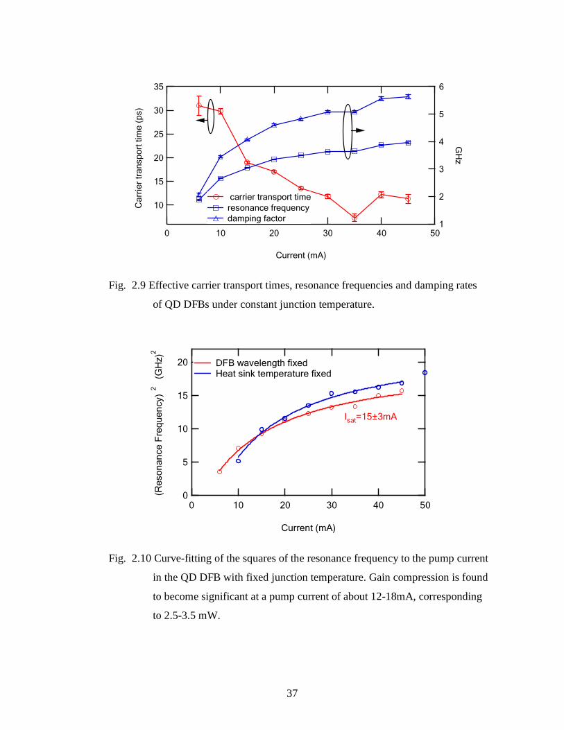
The resonance frequency and damping rate at a fixed DFB wavelength are presented in
Fig. 2.9, showing a difference less than 10% from the case with fixed heat sink
temperature as presented in Fig. 2.3. The effective carrier transport time at high pump is
10 ps, the same as the value without the DFB wavelength control. This indicates that
carrier transport time at high pump is not sensitive to the junction-temperature change
originating from the current injection. A curve fitting based on Eqn. (3.3) is shown in Fig.
2.11 and Isat is found to be 15 ± 3 mA with an effective threshold current about 2.7 ± 0.7
mA. Since the variation of the slope efficiency with temperature can be ignored as
indicated in Fig. 1.7 and Fig. 1.8, a gain-compression output power, Psat, of 2.5 - 3.5 mW
can be found corresponding to the 15 ± 3 mA current. Compared to the 3.3 – 4.1 mW
value determined without the junction-temperature control, we can conclude the thermal
36
effects do not significantly affect the gain compression coefficient measured in previous
section.
2.5. Conclusion
In conclusion, the high-speed performance of QD DFBs is measured and the 3-dB
modulation band width is found to saturate at about 5 GHz in the case of ground state
single mode lasing. The curve-fittings of the small signal responses give the resonance
frequency and damping factor under different pump levels, from which the gain
compression coefficient is determined to be 3-4 × 10-16 cm3 in QD DFBs. This strong
gain compression makes the modulation bandwidth saturated at about 5 GHz. It is also
found that neither the K factor nor the carrier transport time limits the modulation
bandwidth of the QD DFBs. Finally, by fixing the DFB wavelength, the thermal effects
from the junction temperature changing are also checked to have an ignorable impact on
the gain compression coefficient determined by this high speed measurement. Therefore,
reducing the gain compression effects is crucial to improve the high speed performance
of QD devices. A new physical origin for the enhanced gain compression, abrupt gain
saturation, has been proposed and quantified in these QD DFB lasers. Analytical
expressions have been derived to explain the physical phenomenon making rapid and
simple device characterization possible.
37
& #$ #
&'
-./
#$
#$2+,
2$
Fig. 2.9 Effective carrier transport times, resonance frequencies and damping rates
of QD DFBs under constant junction temperature.
)#$*+,-./
&'
<#5:'
1*4 2 ".# =2 "
Fig. 2.10 Curve-fitting of the squares of the resonance frequency to the pump current
in the QD DFB with fixed junction temperature. Gain compression is found
to become significant at a pump current of about 12-18mA, corresponding
to 2.5-3.5 mW.
38
Chapter Three. LINEWIDTH OF QD DFBS
3.1. Introduction
Since the invention of the first laser, the spectral purity of the lasing mode has always
been one of the most central interests. Although typically gas- and solid-state lasers show
a narrower linewidth than semiconductor lasers, the former are inferior when their cost,
size and reliability are considered. Much research has been conducted on narrow
linewidth semiconductor lasers. Different device designs, such as the external cavity
configuration [88-90] and chirped grating DFBs [91,92], have been proposed to achieve
narrow linewidth. Meanwhile, new semiconductor materials, for instance, strained QWs
[93] and finally QDs, have been proposed for narrow linewidth operation because of
their the low internal loss and small linewidth enhancement factor. Therefore, studies of
the linewidth of QD lasers are important. In real world applications, single-mode
distributed feedback (DFB) lasers at 1.3 µm with narrow spectral linewidth are essential
for various applications, such as coherent sources and local oscillators for communication
systems [94].
As discussed in the previous chapter, 1.3 µm devices based on InAs/InGaAs “dots-in-a-
well” (DWELL) technology have become promising alternatives to lasers built on InP-
based materials, due to their low substrate cost, excellent temperature performance, low
threshold current and small linewidth enhancement factor. Theoretical calculations also
show that the population inversion factor, nsp, is lower in QDs than in QWs [30]. These
advantages of QDs over QWs suggest that QD lasers can have narrow linewidth,
considering

39
)1(4
2
0
απ
ναν +
Γ=∆ sp
mtgth nP
hvg (3.1)
where ∆ν is the linewidth, gth is the threshold gain, P0 is the optical output power, Γ is
the confinement factor, vg is the group velocity, αm is the mirror loss, and hν is the
photon density [87].
Theoretically, narrow linewidth is always obtained by increasing the laser power as
indicated by Eqn. (3.1). In real cases, however, the minimum achievable linewidth is
typically limited by the linewidth rebroadening or floor due to the mode instability [95],
existence of side modes [96], spatial hole burning [91,97] and the gain compression
[98,99].. The first three effects are mostly related to the device structure and can be
minimized or eliminated by optimizing the device design. The gain compression is
fundamentally related to the time scales for the carrier equilibrium dynamics in the
semiconductor gain media and is enhanced in QD gain media. Therefore, to understand
the pros and cons of QDs device for narrow linewidth is essential research that motivates
the experiments described in this chapter.
3.2. Devices and experimental setup
The linewidth of three loss-coupled QD DFBs with different gain offsets and a
commercial 1.3 µm index-coupled QW DFB from Mitsubishi, Inc. are studied in this
chapter. The gain offset is defined as the difference between the DFB wavelength and the
gain-peak wavelength. The cavity length of the QD and QW DFBs is 300 µm. The static
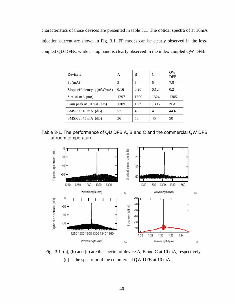
40
characteristics of those devices are presented in table 3.1. The optical spectra of at 10mA
injection current are shown in Fig. 3.1. FP modes can be clearly observed in the loss-
coupled QD DFBs, while a stop band is clearly observed in the index-coupled QW DFB.
Device # A B C QW DFB
Ith (mA) 3 5 6 7.8
Slope efficiency η (mW/mA) 0.16 0.20 0.12 0.2
λ at 10 mA (nm) 1297 1309 1324 1305
Gain peak at 10 mA (nm) 1309 1309 1305 N.A
SMSR at 10 mA (dB) 57 48 41 44.6
SMSR at 45 mA (dB) 56 53 45 50
Table 3-1. The performance of QD DFB A, B and C and the commercial QW DFB at room temperature.
Fig. 3.1 (a), (b) and (c) are the spectra of device A, B and C at 10 mA, respectively.
(d) is the spectrum of the commercial QW DFB at 10 mA.

41
Fig. 3.2 The experimental setup for the self-homodyne linewidth measurement of
QD DFBs.

42
>
2 $$,#
3"
333
*+,./
'
'
'
'
Fig. 3.3 The self-homodyne spectra and their Lorentzian curve-fittings of QD DFB
device B at different pump levels.
>
2 $$,#
"
*+,./
01*
'
'
'
'
'
Fig. 3.4 The self-homodyne spectra and their Lorentzian curve-fittings of the commercial 1.3 µm QW DFB.

43
The linewidth is measured with the self-homodyne technique [100] using a fiber
interferometer with a 3.5 µs delay. The experimental layout is shown in Fig. 3.2. An ILX
lightwave LDP-3620 ultra-low-noise current source is used to avoid excess noise from
the pump source. When a current source without noise control, ILX lightwave 3811, is
used, the linewidth is measured to be 40 MHz, instead of the sub MHz when the low-
noise current source is used. The heat-sink temperature is controlled to be 20 °C. To
avoid the external feedback into the DFBs, two cascaded isolators are applied for
isolation better than 60 dB. In addition, the fiber end in the coupling system is angle
polished. The absence of sensitivity to external feedback is confirmed by the fact that the
measured linewidth does not change even when the tilted angle of the coupling fiber is
varied by about 3 degrees.
3.3. QDs for narrow linewidth operation
The self-homodyne spectra of device B biased at different pump levels are shown in
Fig. 3.3 with their Lorentzian curve-fits. Although the spectral tails at high pump levels
fall off faster than the fitted Lorentzian functions, the parts of the spectra within 3 dB
from the peak still deviate less than 1% from ideal. This suggests that there are small
non-Lorentzian components in the noise of the devices. For the case of the QW DFB, the
non-Lorentzian tale is not observed as illustrated in Fig. 3.4. The origin of the non-
Lorentzian linewidth in these QD devices is unclear at present.
Fig. 3.5 shows the linewidths and SMSRs of the three QD DFBs as a function of the
optical output power. The linewidth-power product of devices A and B is about 1.2 MHz-
mW for the output power less than 2 mW, which is more than an order of magnitude

44
smaller than the value of 16 MHz measured in the commercial QW DFB at 2 mW output
with the same setup, while the typical linewidth-power product in QW DFBs is tens of
MHz – mW depending on the cavity length [87]. This result is physically consistent with
the properties of the QD gain media discussed in the introduction section, as well as the
implementation of the loss coupled grating, which reduces the adverse spatial-hole-
burning effect [13], and the HR/HR coatings that lower the threshold gain. In device C,
due to its larger gain offset and therefore larger α0, a wider linewidth at low power
compared to device A and B is observed.
Table 3-2 Estimating the figure of merit for narrow linewidth in QD DFBs
23)1(
output1mW at mW -MHz 8.0)1(4
)(
:productpower -Linewidth
facet one fromoutput islight theofmost since 1,F :factor couplingOutput
12 :gain modal thresholdDFB
3.5)(14.0
11.0 :loss grating DFB
0.14mW/mA :DFBs QD of efficiency Slope
mW/mA 0.25 :FPs QD of efficiency Slope
2 :loss Internal
7.4)1
ln(2L
1 :LossMirror
2
22
1
1grating
FP
1i
1
21m
=+
=+Γ
=∆
=
=Γ
=+=
++∝=
+∝=
≈
==
−
−
−
−
α
απ
ναν
ααα
ααααη
αααη
α
α
sp
spmgth
linewidht
th
mi
gratingmi
mDFB
mi
m
n
nhFvg
P
cmg
cm
cm
cmRR
45
To understand the narrow linewidth of the QD DFBs, threshold modal gain, mirror loss
and nsp(1+α2) is estimated and compared to the values of typical QW DFBs. By knowing
the internal loss, mirror loss and the slope efficiency of the QD FPs with the same facet
coatings on the same wafer processed for QD DFBs, the threshold DFB modal gain and
nsp(1+α2) are estimated to be 12 cm-1 and 23, respectively, from the fact that device A has
a linewidth-power product of 800 KHz-mW at an output power of 1mW. For a
comparison, Fig. 3.7 shows the values of nsp(1+α2) in different semiconductor gain media.
Since both small nsp(1+α2) and low threshold gain are required for narrow linewidth
operation, QDs are advantageous compared QWs. Fig. 3.7 suggests that the narrow-
linewidth operation is improved by a factor 4-5 in quantum dot DFBs due to the unique
material properties of QDs.
3.4. Linewidth re-broadening in QD DFBs: gain compression
As the output power is further increased, we can observe that a linewidth floor of 500-
600 kHz is achieved in device B for optical outputs of 3-10 mW. Although device A
shares the same property of low linewidth-power product in device C, its linewidth re-
broadens instead of reaching a floor. Those phenomena are presented in Fig. 3.5. In each
device, it is notable that the linewidth rebroadens or minimizes even as the SMSR is
improving and greater than 50 dB as demonstrated in Fig. 3.5. Thus, the origin of the
broadening is not related to the mode competition caused by the degradation of SMSR.
Since the loss-coupled grating reduces the non-uniformity of the optical power
distribution along the cavity compared to the λ/4 phase-shifted quantum well DFB,
spatial hole burning cannot underlie the linewidth behavior of these QD DFBs. As shown

46
in Chapter 2 from the small-signal response, the gain compression is strong in these QD
devices. For the QD DFBs, the linewidth floor starts to occur at an output power of 2-4
mW, approximately the same as the value of the gain saturation power we derived from
the small signal modulation. For the output power of 2-4 mW, at which the linewidth
nonlinearity becomes significant in these devices, an inside-cavity photon density S of
1.2-2.4×1016 cm-3 is found using Eqn. (2.33) in [87] for which a mode volume of 440
µm3 and a mirror loss of 4.8 cm-1 are calculated for these lasers. From this S value, the
gain compression coefficient of these QD devices is estimated to be 4-8×10-16 cm3, which
is more than 30 times higher than the typical value of QWs and is consistent with both
the value of 4×10-16 cm3 published by D. Bimberg et. al. [9] and value of 3-4×10-16 cm3
from the high speed measurement in Chapter 2. It is worth mentioning that no significant
linewidth re-broadening or floor is observed in the commercial QW DFB with an
improving SMSR as shown in Fig. 3.6, clarifying that the linewidth re-broadening is not
from the testing setup.
As discussed in Chapter 2, the amplitude of FP modes around the excited states keeps
increasing as the output of the QD DFBs rises. It is crucial to investigate if the amplified
spontaneous emission (ASE) of the excited states contributes to the linewidth
rebroadening or floor mentioned above, since the self-homodyne technique collects all
the light from the DFBs. Therefore, an optical filter is introduced to filter out the excited
state emissions and repeat the linewidth measurement. When the bandwidth of the filter
is varied from 0.5 to 10 nm, the measured linewidth differs less than 3% as shown in Fig.
3.8. This excludes the possibility that the linewidth rebroadening and floor result from the
increasing ASE of the excited states.

47
3.5. Effects of gain offset on the linewidth rebroadening
It was noticed by G. P. Agrawal that the alpha under gain compression changes
differently as a function of the gain offset [98], that is, the position of λDFB relative to the
gain peak. From the master equations describing the interactions of the photon-carrier
system and carrier thermal equilibrium dynamics, the effective linewidth enhancement
factor was derived to be:
)2/()1())(
()(
110 SSS
d
dg
gS
L
inLeff εεε
ωω
τωεαα ωω ++++= = (3.2)
here α0 is the linewidth enhancement factor without gain compression effects, ε is the
gain compression coefficient, S is the photon density, g(ω) is the small signal gain, ωL is
the lasing frequency and τin is the carrier dephasing time. Eqns. (3.1) and (3.2) show that
the linewidth can re-broaden, reach a constant (floor), or narrow down faster than 1/P
with increasing power, depending on the sign of dg(ω)/dω as determined by the offset of
the DFB mode relative to the gain peak. The effects of gain offset indicated by Eqn. 3.2
are found applicable to the linewidth floor in device B (dg(ω)/dω~ zero) and the
rebroadening in device C (dg(ω)/dω positive), but not to the rebroadening in device A
which has a blue-shifted gain offset. Theoretically, dg(ω)/dω should be negative in this
region of the gain spectrum and a linewidth narrowing faster than a 1/P dependence
should occur if the QD ground state is sufficiently isolated from other states. However, it
is believed that the blue-shifted offset of device A is subject to the homogeneous and
inhomogeneous broadenings from the excited states which causes an increase of the alpha
[16], and that the gain spectrum does not have the inverted parabolic shape that would be
expected for an idealized QD ground state.

48
3.6. Conclusion
Linewidths of QD LLC DFBs with different gain offsets from QD gain peaks are
investigated and compared to a commercial QW DFB. The linewidth-power product of a
QD DFB with a 300 µm cavity is measured to be less than 1.2 MHz-mW for the output
power less than 2 mW, more than one order less than the typical value of the QW DFB.
Small internal loss, low mirror loss and low nsp(1+α2) are the contributing factors for this
significant improvement. The nsp(1+α2) is estimated to 23 in QDs with a modal gain
around 12 cm-1. It is unique for QDs to achieve this low modal gain and low nsp(1+α2)
simultaneously, while much higher modal gain is required for this low nsp(1+α2) in QWs.
Therefore, QDs are advantageous for narrow linewidth operation compared to QWs. On
the other hand, due to the strong gain compression in QDs, the linewidths are found to re-
broaden or floor at much lower photon density. Although the floor for the output power
of 3-10 mW is 500 KHz, still small compared to typical QW DFBs, the gain compression
is the limiting factor for the further reduction of linewidth at high output power. At the
same time, the excited-state ASE is found not to contribute to the measured linewidth by
applying an optical filter with variable bandwidth to the output of QD DFBs. Finally, the
effects of gain offset of the QD DFBs are discussed. These results suggest that QD LLC
DFBs with a larger mode volume to reduce the effect of gain compression and zero gain
offset will have improved narrow linewidth performance.

49
% 4 ;./
>
>
$4
;)
1 '1 1 &
Fig. 3.5 Linewidths and SMSRs of the three QD DFBs as a function of optical
output power.
>
% 4 ;./
>
$4
;)
µ !
Fig. 3.6 Linewidth and SMSR of a commercial 1.3 µm QW DFB.

50
Fig. 3.7 The figure of merit for the spectral linewidth enhancement in semiconductor
lasers nsp(1+α2) at optical gain peak as a function of the modal gain in bulk
DH, QW lasers with different number of quantum wells [101] and QD
lasers with six stacks of DWELL.

51
Fig. 3.8 Schematic plot for applying an optical filter to exclude the excited-state
ASE from the self-homodyne measurement.
Fig. 3.9 The measured linewidths of the QD DFB device C with different bandwidth
of the optical filter. The linewidths are found to be independent of the filter
bandwidth.
3
3
3
3
3
3
% 4 ;./
* 94
1 &?'
@5$&

52
Chapter Four. QD DFBS UNDER EXTERNAL FEEDBACK
4.1. Introduction
A major problem with semiconductor lasers, both FP and DFB types, is that they are
highly sensitive to the laser light which re-enters the laser cavity after being reflected by
an external reflector. External optical feedback of the laser light usually causes instability
of operation of a laser diode and generates excessive noise in optical communication
systems [102,103]. A variety of optical elements, including lenses, fiber ends and
integrated external cavities, can be the sources of unwanted optical feedback. For these
reasons, costly and bulky optical isolators are typically required in most applications to
protect semiconductor lasers from optical feedback-induced noise.
One of the consequences of the external feedback on a laser is coherence collapse.
When the external feedback excesses a certain level, the laser becomes instable and the
coherence of the laser output is dramatically reduced. The linewidth vs external feedback
level is plotted in Fig. 4.1 from ref. [102], showing a narrowing of the linewidth as a
function of external feedback before the coherence collapse point and a dramatic
linewidth rebroadening after. Associated with the linewidth broadening is the increase of
noise, which is demonstrated in Fig. 4.2. Avoiding coherence collapse is essential for
real-world applications.

53
Fig. 4.1 Coherence collapse of a DFB laser is indicated by the dramatic broadening
of the linewidth [102].
Fig. 4.2 The low frequency noise of a DFB under external feedback with different
linewidth enhancement factors. Noise burst after coherence collapse is
shown [102]. The α in the figure stands for linewidth enhancement factor.

54
The effects of external feedback can be explained in Fig. 4.3. The external feedback
is coupled into the laser cavity through the output facet and causes a perturbation on the
photon density. As described by the rate equations on the small signal modulation, this
perturbation leads to a fluctuation of the carrier density and thus the optical gain. The
variation of gain itself changes the output power and consequently the external feedback
strength. These processes form an intensity fluctuation loop that is effectively a self-
intensity modulation and not sufficient to cause the complex dynamics of the laser system.
On the other hand, since the fluctuations of optical index and gain are coupled by the
linewidth enhancement factor, the external feedback can also introduce the phase
fluctuation loop as indicated in Fig. 4.3. The interaction of the intensity and phase loop
essentially makes the dynamics of the laser system under external feedback very complex
and results in the system instability and even chaos.

55
Fig. 4.3 A schematic presentation of the effects of external feedback on a
semiconductor laser.
4
2
2
22 1
16 αατ +Γ=
e
Recritical
Cf
E field, gain, index Laser diode
|∆E| e-j∆φ
|∆E(t)|, ∆φ(t)
Intensity fluctuation
Gain fluctuation
wavelength fluctuation
Laser dynamics
Alpha
Cavity coupling
phase
Intensity
Index fluctuation
Cavity resonance

56
Fig. 4.3 also indicates the possible approaches to increase the external feedback
resistance. First of all, to reduce the coupling of the laser diode to the external cavity will
effectively reduce the external feedback strength. HR coated facets will help to diminish
this coupling. Secondly, if the laser dynamics are heavily damped, the gain fluctuation
introduced by the photon-density variation can be suppressed. Therefore, a large damping
factor will increase the external-feedback resistance of the laser. Thirdly, we need to
decouple the interaction between the intensity and phase loops by minimizing the
linewidth enhancement factor (or alpha parameter). Finally, longer cavities have less
change of the lasing wavelength for the same amount of phase fluctuation caused by the
external feedback.
Petermann introduced a parameter to characterize the external feedback sensitivity:
the critical external-feedback level for coherence collapse [102]:
4
2
2
22 1
16 ααγτ +=
e
Lcritical
Cf (4.1)
where τL is the round trip time of the laser cavity, γ is the damping factor of the laser, Ce
is the cavity coupling factor and α is the linewidth enhancement factor. Ce is related to
the facet reflectivity and is equal to (1-R)/(2R1/2) in the case of FP lasers. Compared to
QWs, we can expect the improvement of external feedback resistance in QDs, since the
much stronger damping and possibly smaller alpha as discussed in previous chapters.
From the device point of view, the loss coupled grating, which is less subject to the
spatial hole burning due to the more uniform distribution of the optical intensity along the
cavity compared to conventional quarter-wavelength shift index coupled gratings, and the
HR coated facet are also beneficial to improve the external feedback resistance. The

57
motivation of this chapter is to investigate the behavior of the device under external
feedback and demonstrate the improvement in the external feedback resistance in LLC
QD DFBs.
4.2. Experimental setup
The setup for the feedback experiment is shown in Fig.4.4. The laser output is coupled
into a 3 dB optical fiber coupler. The feedback ratio is controlled by a variable optical
attenuator, which gives attenuation from 1.5 dB to 80 dB. A film of 5000
Au is
evaporated onto the flat fiber end of one arm of the coupler and functions as a reflective
mirror. The distance between the laser and the external reflector is about 7 meters. It is
noteworthy that the critical external feedback level for coherence collapse does not
depend on the distance between the external reflector and the output facet of the device.
To avoid excess uncontrolled feedback, the coupling lens is AR coated and the fiber ends
are angle-polished in all connections. The external feedback ratio, which is defined as the
ratio of the power reflected back to the laser facet and the single-facet output power of
the device, is calculated as follows:
ΓdB = P1(dBm) – P0(dBm) +CdB (4.2)
where the P1 is the reading from the power meter in Fig. 4.4, P0 is the output power of the
laser and CdB is the -3.4 dB coupling loss from the semiconductor laser to the fiber. The
coupling loss CdB is determined by the ratio between the total power after the 3dB optical
coupler (assumed loss-less) and the output power directly measured at the facet of the
DFB. The polarization controller is adjusted to obtain the maximum feedback effect to
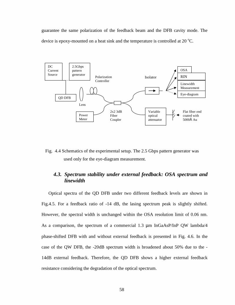
58
guarantee the same polarization of the feedback beam and the DFB cavity mode. The
device is epoxy-mounted on a heat sink and the temperature is controlled at 20 oC.
Fig. 4.4 Schematics of the experimental setup. The 2.5 Gbps pattern generator was
used only for the eye-diagram measurement.
4.3. Spectrum stability under external feedback: OSA spectrum and linewidth
Optical spectra of the QD DFB under two different feedback levels are shown in
Fig.4.5. For a feedback ratio of -14 dB, the lasing spectrum peak is slightly shifted.
However, the spectral width is unchanged within the OSA resolution limit of 0.06 nm.
As a comparison, the spectrum of a commercial 1.3 µm InGaAsP/InP QW lambda/4
phase-shifted DFB with and without external feedback is presented in Fig. 4.6. In the
case of the QW DFB, the -20dB spectrum width is broadened about 50% due to the -
14dB external feedback. Therefore, the QD DFB shows a higher external feedback
resistance considering the degradation of the optical spectrum.
Power Meter
QD DFB
Variable optical attenuator
OSA
Linewidth Measurement
Eye-diagram
DC Current Source
2.5Gbps pattern generator
Polarization Controller
Flat fiber end coated with 5000Å Au
Isolator
2x2 3dB Fiber Coupler
Lens
RIN

59
For a higher resolution measurement, the linewidth of the DFB laser is determined by
self-homodyne technique [104] with a fiber interferometer having a fixed delay of 3.5 µs.
The linewidth with an external feedback ratio below -60 dB is 650 kHz at 5 mW output.
As the feedback ratio increases, the linewidth narrows down quickly until the feedback
ratio reaches -14 dB, where the linewidth rebroadening occurs due to the coherence
collapse. However, the laser linewidth under -14 dB feedback is still less than 20 kHz,
much less than the 650 kHz free-running linewidth. This result confirms the unchanged
spectrum measured by OSA. For comparison, the critical coherence collapse feedback
ratio of an index-coupled QW DFB is typically between -20 and -30 dB [1, 11], which we
also confirmed in Fig. 5.8 by a measurement of the commercial QW DFB. For the
802.3ae 10 Gbps Ethernet standard, the laser must tolerate up to -12 dB feedback from
the network. For typical coupling losses of 4-6 dB in fiber-pigtailed lasers, a feedback
ratio of -14 dB at the laser facet corresponds to -2 to -6 dB feedback from the system.
Thus, the QD LLC-DFB has the potential to operate as an isolator-free light source in
fiber-optic communication networks.

60
Fig. 4.5 The optical spectra of the QD LLC DFB with -14 dB and less than -60 dB
external feedback. No significant broadening is observed with the
resolution of the optical spectrum analyzer to be 0.06nm.
Fig. 4.6 Spectra of the commercial QW DFB with -15 dB and less than -60 dB
external feedback. Significant broadening is observed.
4
29=A29=
4 9$9,BC$$ $
>>3>3>3>3>3>3
01%%&1*"29=5"29=A

61
Fig. 4.7 Self-homodyne spectra of the QD DFB under different external feedback
strength, while linewidth re-broadening occurs at -14dB.
Fig. 4.8 Self-homodyne spectra of the commercial QW DFB under external feedback
strength, the linewidth re-broadening at -20dB external feedback can be
clearly observed.
>
2 $$,#
3"
3333333
*+,./
*9= $A
*9= $D
*9= $5
*9= $5
9=$*9= $5

62
Fig. 4.9 The noise spectrum of the QD LLC DFB before coherence collapse. Low
frequency noise is the dominant component of the spectrum.
Fig. 4.10 The noise spectrum of the QD LLC DFB at coherence collapse. The spikes
at integer multiples of the relaxation frequency in the noise spectrum are
the indications of the coherence collapse.
C$ ##
">
*+,./
"29=
C$ ##
">
*+,./
"29=

63
<# ,C$ #
">
*+,./
329=2#C$ #9=$
; #9 # 01*
<# ,C$ ##
">
*+,./
329=2#)<CE9=$E
011*
Fig. 4.11 The noise spectra of the QD LLC DFB and the QW DFB under coherence
collapse introduced by external feedback. QD LLC DFB shows a lower
noise level compared to the commercial QW DFB.
64
4.4. DC Noise of QD DFBs under external feedback
The noise of the QD LLC DFB is also investigated with external feedback. At weak
external feedback, low frequency noise (<1 GHz) is found dominate in the noise
spectrum of the QD LLC DFB as shown in Fig. 4.9. This is consistent to the observations
reported in ref. [103]. As the external feedback is further increased into the coherence
collapse regime, spikes at the integer multiples of the relaxation frequency become
significant in the spectrum in Fig. 4.10. This is an indication of the complexity of the
laser dynamics. This noise measurement also confirms that the critical external feedback
level for coherence collapse is -14 dB. In Fig. 4.11, the noise spectra of the QD LLC
DFB and index-coupled QW DFB under -14 dB external feedback are compared. The
RIN in the QW DFB is about 7 dB higher than in the QD DFB, indicating a higher
resistance to the external feedback in the case of QD DFBs.
4.5. Degradations of signal to noise ratio and jitter under external feedback
It is possible, however, that the degradation of the signal to noise ratio (SNR) would
limit the laser performance under feedback at a level significantly less than what is
required to induce coherence collapse [102,103,105]. Eye diagrams under 2.5 Gbps
modulation are shown in Fig. 4.12 for the QD DFB feedback of (a) -60 dB, (b) -20 dB
and (c) -14dB respectively. Both of the ‘1’ and ‘0’ levels are appreciably broadened when
the feedback changes from -60 dB to -14 dB due to the excess intensity noise induced by
the external feedback. The signal to noise ratio of the eye diagram with different
feedback ratios is shown in Fig. 4.13. We use a commercially-available QW DFB as
reference. Both the lasers have an output power of 5mW and an extinction ratio of 6.6 dB.

65
The QW DFB has a higher SNR at low levels of feedback than the QD DFB although we
believe that this is not an inherent feature of the QD technology since a RIN as low as -
146 dB at an output power of about 4 mW was measured in these devices. It is obvious
that the commercial QW DFB signal to noise ratio (SNR) starts to degrade at a feedback
ratio of -50 dB, which is the same value reported in the literature for the feedback that
causes excess noise in typical QW DFB’s [105]. In contrast, the SNR of the QD DFB
starts to degrade at a feedback level around -30 dB. This result amounts to about 20 dB
improvement of the feedback resistance in the QD DFB. The shoulder near -22 dB on the
QW DFB curve in Fig. 4.13 is due to the coherence collapse. The signal to noise ratios of
the QD LLC-DFB under -20 dB and -14 dB external feedback are 8.3 and 6.0, and the
bit-error-rate (BER) are theoretically calculated to be 4x10-17 and 10-9 respectively [106].
For the typical fiber coupling efficiency mentioned above, the QD DFB should still be
able to tolerate network feedback in terms of maintaining sufficient SNR without an
isolator.

66
Fig. 4.12. The eye-diagram of the QD DFB under 2.5 Gbps modulation with
different external feedback levels.
Fig. 4.13. The root-of-mean-square jitter and signal-to-noise ratio (SNR) of the QD
LLC DFB and QW DFB under different external feedback ratios. Although
the degradation of the jitter is more same for the two devices, the SNR of
the QD DFB starts to degrade under -30dB external feedback, about 20 dB
improvement compared to the QW DFB.
);F #
!"29= $
$
C$# ) $
01
0
01
0
Feedback: -60dB -20dB -14dB

67
Chapter Five. CHIRP OF QD DFBS
5.1. Introduction
To explore the potential of QD DFBs for communication systems, knowledge of the
optical spectrum of the devices under modulation is critical. The optical spectrum of a
modulated laser typically gets broadened due to the direct intensity modulation and the
resulting frequency chirp. Chirp has two major detrimental outcomes in a typical
transmissions system. The first is that the chirp can interact with the fiber dispersion to
create a power penalty, which ultimately limits the number of channels or the distance
over which the signal can propagate in today’s wavelength division multiplexed (WDM)
systems. The second is that chirp can broaden the transmitted spectrum limiting the
channel spacing by interfering with adjacent channels even in a short-haul ultra-dense
WDM environment. Therefore, low chirp semiconductor lasers have been of interest for a
long time [107-112]. The development of quantum dot lasers has been expected to
improve the chirp characteristics considering the small linewidth enhancement factor
[113,114].
QD lasers with a frequency chirp one order of magnitude lower than that of QW lasers
were demonstrated in ref. [113]. Grown by MBE, the QD lasers are designed for high
aspect ratio (height/base diameter), so that the ground state is well separated from the
first excited states by about 70 meV, which is larger than the room-temperature thermal
energy. The gain medium consists of three InAs QD layers but the gain is still low.
Therefore, 97% HR coatings on both facets and a cavity length of 970 µm are necessary
to lower the threshold gain. This low threshold gain can reduce the adiabatic chirp of the
68
devices [115]. Although these devices show a good chirp performance, they are less
desirable for practical applications in terms of the lasing wavelength (1.2 µm), low output
power (~0.1 mW) and low slope efficiency (0.01 mW/mA). Furthermore, due to the
limitation of the device performance and experimental setup, the authors only
qualitatively compared the chirp of QD to QW FP lasers and no quantitative
measurement is carried out to investigate the alpha factor and gain compression
coefficient in the QD devices.
Due to the relatively low modal gain of the QD gain media, multiple stacks of QDs are
necessary for good high-speed performance. The multi-stack structure increases the
inhomogeneous broadening and thus the linewidth enhancement factor [16]. The alpha
factor also becomes larger when the excited states are populated [16], which is severe
considering the typical spacing between the ground state and the first excited state is
around 45 meV for 1.3 µm QDs as shown in Chapter.1. Moreover, the strong gain
compression in QDs demonstrated in previous chapters makes the alpha factor power-
dependent and become large at elevated outputs. The adiabatic chirp is also expected to
be large due to the gain compression. It is crucial to understand the effects of these
factors on the chirp performance of QD lasers. On the other hand, a quantitative time-
resolved-chirp measurement is possible [116] as a result of the single-mode operation and
several mWs output power of the QD LLC DFBs. This offers, for the first time as we
know, an opportunity to study the alpha factor and gain compression in a device above
threshold, which can be much different from the values measured below threshold [7,16].
The motivations of this chapter are to measure the chirp and thus estimate the alpha

69
factor and gain compression coefficient of the QD LLC DFBs. The definition of the gain
compresson coefficient is given in Eqn. (2,4).
Chirp is the drift of the optical wavelength of a laser under direct intensity modulation.
The rate equations describing the photon density and frequency of a laser are given as
following:
(5.2) )(4
)(4
)(
(5.1) )1
(
thgthgththth
th
spthg
Ggvggvggg
n
nn
n
RSGS
gv
dt
dS
−Γ=−Γ=−∂∂−=∆−=−=∆
+−+
Γ=
πα
παυυυυυ
ε
where Γ is the confinement factor, vg is the group index, g is the material gain, S the
photon density, εs is the gain compression factor associated with the photon density, Gth
is the temporal threshold gain, Rsp the spontaneous emission rate, α the linewidth
enhancement factor, ν is the lasing frequency, νth is the frequency at threshold. After
solving Eqn.(5.1) for Γvgg and putting it into Eqn. (5.2), we can have:
( ) ( )
( )( )
( )( ) (5.3) ]1
[4
1
]1
[4
1
]1
1[4
P
PG
Pdt
dPP
S
SG
Sdt
dSS
S
RSSG
Sdt
dSS
P
thPP
s
thss
spsthss
εε
πεα
εε
πεα
εεε
παυ
+++=
+++≈
+−++=∆

70
with P is the output power of the device, εP the gain compression coefficient associated
with the output power. The spontaneous emission term is ignored since the laser operates
well above the threshold. Since the gain compression is not severe in most of the QW
lasers, that is εpP << 1, people typically approximate Eqn. (5.3) into:
(5.4) 44
thPPGPdt
dP επ
απ
αυ +≈∆
with the first term, proportional to the derivative of the optical power, dubbed as transient
chirp and the second term, proportional to the optical power itself, as adiabatic chirp
[115]. Compared Eqn (5.3) and (5.4), the effective alpha considering the effects of gain
compression can be expressed as:
)1( PPeff εαα += (5.5)
with the transient chirp is the dominant component in most of the QW lasers. It is notable
that the adiabatic chirp is directly related to the gain compression coefficient and
threshold gain of the lasers.
Equation (5.4) is well known for the measurement of alpha and the compression
coefficient in QW lasers [115,117]. Since the gain compression effect is stronger in QDs
than QWs, we use Eqn. (5.3), instead of Eqn. (5.4), to describe the chirp in QD DFBs. It
is remarkable that Eqn. (5.3) can apply to lasers under large signal modulation. To obtain
a large signal to noise ratio, the laser sources in some communication systems are
digitally modulated with an extinction ratio of about 10 dB for a large separation of ‘1’
and ’0’ levels. The chirp can be still well modeled by Eqn. (5.3) [118].
71
5.2. Time-resolved chirp: Experimental setup and technical background
The time-resolved chirp (TRC) is a technique to measure the wavelength chirping
directly in the time domain. The wavelength chirp, ∆ν, of a laser under external
modulation is measured in real time, while the output of the laser, P, is also recorded
simultaneously. Based on the relation between ∆ν, P and dP/dt expressed in Eqn. (5.3),
the alpha factor and the gain compression coefficient can be extracted.
The experimental setup for TRC is given in Fig. 5.1. The pseudo-random pattern
generator (PRPG) generates a 2.5 Giga-bit-per-second (Gbps) pseudo random ‘0’ and ‘1’
data string with a length of 27-1. The optical filter in the OSA, originally designed for the
monochromatic output, is used as a wavelength discriminator which transfers the
wavelength chirping into optical intensity variation. The band pass of the optical filter is
adjustable and has a minimum resolution of 0.04 nm, that is, 7.12 GHz at the wavelength
of 1.3 µm. If the band pass is set to be much larger than the spectral width of the
modulated light, the OSA will transmit all of the spectral components and just convey the
same output from the modulated DFBs, without spectral filtering, to the digital
communication analyzer (DCA). Then the DCA records the un-filtered and filtered
optical signals from the OSA with the information of the variations of the output power
and wavelength chirping, respectively, in time domain. Since the PRPG and DCA are
synchronized by the trigger output from the PRPG, the chirp and the optical intensity of
the laser output can be aligned up in time domain, so that alpha factor and gain
compression can be obtained based on Eqn. (5.3).

72
Fig. 5.1 The experimental setup for TRC measurement [116]. The QD DFB is
modulated by the pattern generator and its wavelength chirping is
translated into optical intensity variation and then recorded by the DCA.
Fig. 5.2 A schematic drawing of the measurement of the wavelength chirping with
the optical filter built in to the OSA [116].

73
The wavelength chirping is measured by the wavelength discriminator method [119]
utilizing the very low dispersion monochromator of the 86146B OSA. Referring to Fig
5.2, the monochromator filter is step-tuned through the modulated laser wavelength. The
lowest wavelength, λ1, and the highest wavelength, λN, are set to fully tune through the
chirped spectrum to achieve a 30-dB amplitude drop on each side of the filter response.
At each wavelength, an intensity vs. time record of length M is measured on the DCA.
The resulting collection of data contains the chirp information in an N by M matrix as
shown in Fig. 5.2. For each row in the matrix, a weighted-average wavelength value of
δλ(t) can be calculated based on the following algorithm with f(x) the transfer function of
the optical filter.
Since the transfer function is symmetric about the center wavelength, λ0, and the
transmission for the wavelength far away from λ0 is vanished, f(x) can be expressed as:
0)(),( 0
00 →−= ∞→−λλλλλλ ff (5.6)
with λ the wavelength of the light input to the filter. Then the matrix element Ai,j given in
Fig. 5.2 can be calculated from the f(x) as:
)(),( ,0,0, jtijtiji ffA == −== λλλλ (5.7)
with λ0,i denotes the center wavelength at the i-th step-tune of the optical filter and λt=j
the wavelength of the modulated DFB laser at time j. Therefore, the wavelength chirp can
be obtained from the matrix Ai,j:
=
=
−=
N
iij
N
isiij
A
At
1
1
)()(
λλδλ (5.8)
based on the following property of the matrix A:

74
=
==
∞
∞−=
∞
∞−===
∞
∞−===
∞
∞−=
=
=
≈
−−=
−−+−−−=
−≈
Ni
ijijt
ttjt
jtjtjtjtjtjt
jto
Ni
iiji
A
df
dfdf
dfA
0,
00
00000
000
,0,
)()(
)()()())((
)(
λ
λλλλλ
λλλλλλλλλλλ
λλλλλ
(5.9)
The LIV curves of the QD DFB tested are shown in Fig. 5.3. The threshold of the
device is 5 mA and the slope efficiency is approximately 0.1 mW/mA. The resistance of
the device is calculated to be 20.6 Ohms in the range of 10 mA – 40 mA DC bias. As the
output of the pattern generator is designed to be voltage, the resistance is used to convert
the voltage modulation-amplitude approximately into a current one. The device has a side
mode suppression ratio of about 50 dB with a DFB wavelength of 1320 nm. All the
testing is done with the heat sink temperature controlled to be 20 oC. Two 30-dB isolators
are cascaded to avoid unintended external optical feedback.
5.3. Chirp with a fixed extinction ratio of modulation.
The extinction ratio of a digitally modulated signal is defined as the ratio between the
power levels at the ‘1’ and ‘0’ states. For communication systems, a large extinction ratio
is preferred to overcome the penalties of the transmission loss and noise. In this part of
the experiment, we measure the chirp of the QD DFBs biased at different DC currents
with the amplitudes of the digital modulations adjusted to keep an extinction ratio of
about 10 dB. The eye diagram of the DFB output at 20 mA is presented in Fig. 5.4 with

75
an extinction ratio of 9.48 dB and shows no touching on the 2 Gbps internet standard
mask. Since the rise time is estimated to be 120 ps and the fall time about 180 ps based
on Fig. 5.2, we can conclude that the interference between the two ‘1’ bits separated by
a‘0’ bit is ignorable. This helps to eliminate the dependence of the measured chirp on the
modulation pattern. Another significant feature of the eye diagram is that no overshoot is
observed at the rising edge, indicating a reduced transient chirp. This is consistent with
the strong damping rate from the high-speed measurement presented in Chapter 2.
3
3
3
3
$
&'
3
3
3
3
3
3
($(
Fig. 5.3 LIV curves of the QD DFB for the TRC measurement.

76
Fig. 5.4 The eye diagram of the output of the modulated QD DFB biased at 20 mA
with an extinction ratio of 9.5 dB.
The measured time-resolved chirp and optical power of the QD DFB are given in Fig. 5.5.
The output power of the QD DFB at 20mA is 1.4 mW. The total coupling loss of the fiber
optical isolator and monochromator in OSA is measured to be - 12 dB. The power in Fig.
5.5 is the power output from the monochromator. The time resolved chirp of the QD DFB
shows weak spikes at the rising edges of the modulated optical signal, and, significantly,
the transient chirp does not dominate over the adiabatic chirp. As a comparison, a TRC
result of a QW DFB is shown in Fig. 5.6, showing the dominance of the transient chirp
over the adiabatic chirp. In QD DFBs, the transient chirp is suppressed due to the large
damping factor discussed in Chapter 2 and the adiabatic chirp is enhanced due to the
strong gain compression.
Table 5.1 gives the results of TRC measurement with the extinction ratio around 10
dB. The peak-to-peak voltages, Vpp, is the voltage modulation depth on the QD DFB for

77
the 10dB extinction ration (ER). The effective alpha is defined in Eqn. (5.4) with the gain
compression effect included. The average chirp here is the difference between the
average chirps on ‘1’ and ‘0’ levels. For the chirp is positive at ‘1’ levels and negative at
‘0’ levels, the alpha parameter here is a positive value. For large-signal modulation,
higher order harmonic and nonlinear effects can be significant and cause a shift of the
average optical frequency of the modulated light relative to the un-modulated one [120].
The freq_shift in Table 5.1 gives this parameter, which is an importance factor
determining the cross-talk strength between different channels in WDM communication
systems.
Bias (mA)
Power (mW)
Vpp (V) ER (dB)
Effective Alpha
Avg chirp (GHz)
freq_shift (GHz)
15 0.912 0.57 9.34 5.52 7.55 -0.75 20 1.39 0.84 9.48 6.34 12.65 -1.35 25 1.85 1.15 10.16 7.20 13.83 -1.44 30 2.26 1.4 9.92 7.94 16.03 -1.72 35 2.67 1.64 9.73 8.31 23.06 -2.71 40 3.04 1.93 9.82 9.48 24.54 -2.75
Table. 5-1 The experimental results of the TRC of the QD DFB with the extinction ratio kept around 10 dB.

78
TRC Result
-15.0E+9
-10.0E+9
-5.0E+9
000.0E+0
5.0E+9
10.0E+9
000.0E+0 1.0E-9 2.0E-9 3.0E-9 4.0E-9 5.0E-9 6.0E-9 7.0E-9 8.0E-9 9.0E-9
Time (seconds)
Chi
rp (
Her
tz)
000.0E+0
20.0E-6
40.0E-6
60.0E-6
80.0E-6
100.0E-6
120.0E-6
140.0E-6
160.0E-6
Pow
er (
Wat
ts)
Chirp(Hz)
Power(watts)
Fig. 5.5 The chirp and corresponding power measured on the QD DFB biased at 20
mA. The chirp at ‘0’ levels are noisier than ‘1’ levels as a result of the
increased measurement error for lower power.
Fig. 5.6 TRC measurements of the chirp and power of a QW DFB as given in ref.
[121].

79
For an extinction ratio of 10 dB, we have (S+∆S)/(S-∆S)=10, then ∆S/S=9/11. The output
power is proportional to the injection current and thus the voltage, so Vpp ∝ (I-I th). Since
the adiabatic chirp dominates the average chirp, the average chirp ∝ ∆S ∝ S ∝ (I-I th) for a
fixed extinction ratio. The linear dependence of the Vpp and average chirp on the DC bias
is shown in Fig. 5.7. The value of the chirp-per-Vpp is ~ 13 MHz/mV. Considering the 20
Ohms of resistance of the QD DFB, the change in the chirp with current is estimated 260
MHz/mA, comparable to the typical value of QW lasers [122].
The shift of the average optical frequency of the modulated light relative to the un-
modulated one is given in Fig. 5.8. The shift of the center frequency is -1.4 MHz/mV,
approximately 10% of the total chirp. This shift of the center frequency could be related
to the higher order harmonic response of the device to the large signal modulation,
including the non-perfect linearity on the L-I and I-V curves and the higher order
behaviors of gain compression.
The effective of alpha parameter, defined as α(1+εPP) in Eqn. 5.5, is given in Fig. 5.9.
The curve fitting results show that the alpha is ~ 4 at threshold and doubles once the
output power is increased by ~ 2 mW. This is consistent with the linewidth re-broadening
that occurs at about 2-4 mW output in the QD DFBs discussed in Chapter 2.
As a conclusion of this section, the chirp of the QD DFB is measured to be 13 MHz/mV
with a shift of the center frequency of about -1.3 MHz /mV for a fixed extinction ratio of
10 dB. These results show that these QD DFBs have a similar chirp performance as
typical QW DFBs for real communication systems. The alpha at threshold is determined
to be around 4 and doubles when the output power reaches 2 mW.
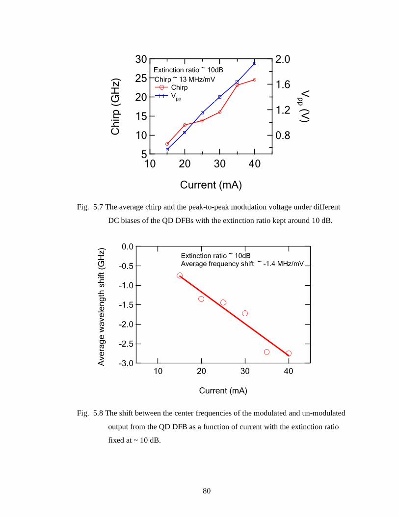
80
& -./
&'
3
3
3
3
( (
!" $ $D
& D;./7(&
(
Fig. 5.7 The average chirp and the peak-to-peak modulation voltage under different
DC biases of the QD DFBs with the extinction ratio kept around 10 dB.
3
3
3
3
3
3
3
'4 # 2-./
&'
!" $ $D'2+,# 2D3;./7(
Fig. 5.8 The shift between the center frequencies of the modulated and un-modulated
output from the QD DFB as a function of current with the extinction ratio
fixed at ~ 10 dB.
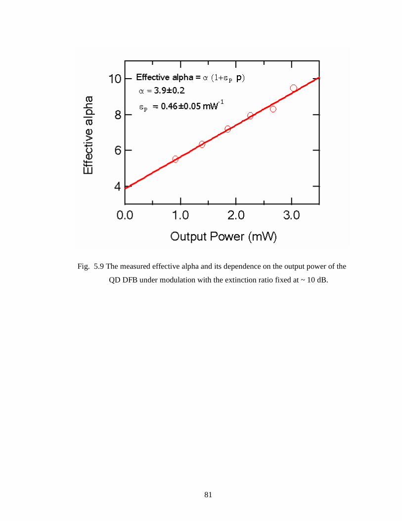
81
Fig. 5.9 The measured effective alpha and its dependence on the output power of the
QD DFB under modulation with the extinction ratio fixed at ~ 10 dB.

82
5.4. Chirp with a fixed modulation depth Vpp
In the previous section, a large signal modulation was used and the alpha measured was
the average over a large range of DC bias. To study the relationship of the dependence of
alpha on the output power, smaller modulation is needed. In this part of experiment, the
time resolved chirp is measured under different biases with the peak-to-peak voltage, Vpp,
of the modulation fixed at 250mV, corresponding to a current modulation with a peak-to-
peak amplitude of about 12 mA. Therefore, the alpha measured here will be an average
value over the (-6mA, 6mA) vicinity of the bias. The experimental results are given in
Table 5.2 with the same definitions for the effective alpha, average chirp and frequency
shift given in Table 5.1.
Fig. 5.10 gives the measured chirps at 15 mA, 25 mA and 35 mA with their curve-fits.
Compared to the chirp under large modulation discussed in the previous section, the
adiabatic chirp still dominates the overall chirp while the transient chirp spikes are further
weakened because of the smaller modulation depth. The curve fittings based on Eqn. (5.3)
are quite good as demonstrated in Fig. 5.10.
The effective alpha is plotted in Fig. 5.10. The alpha factor at threshold is found to be 2.6
± 0.4 and εp 0.7 ± 0.2 mW-1 by curve-fitting the measured effective alpha as a linear
function of the output power.based on Eqn. 5.5. The alpha factor is lower and εp is larger
than the values we got from the modulation with extinction ratio fixed at 10 dB. This can
be explained by the fact that the measured alpha and εp are averaged over a smaller range
of the DC bias and that their dependence on the output power is significant. The alpha
factor without the gain compression effects is close to the results in Ref. [16] and doubles
when the output power is 1-2 mWs.

83
Fig. 5.12 gives the gain compression coefficient of the QD DFBs. The curve-fitting error
bar comes from the large signal modulation and the sensitivity of the derivative dP/dt to
the measurement noise. The gain compression factor is estimated to be 0.2 ± 0.1 mW-1
from the curve-fitting based on Eqn. 5.3. Therefore, roughly speaking, the gain
compression becomes significant for an output power of 7 mW, comparable to the 2-5
mW estimated from the linewidth and high-speed experiments, and the gain compression
photon density, εs, is still one order of magnitude lower than the typical value of QWs.
However, the gain compression coefficient εp = 0.2 ± 0.1 mW-1 determined here is
smaller than the value of εp = 0.7 ± 0.2 mW-1 determined from the dependence of alpha
factor on the output power. This could be explained the enhancement of the gain
compression by the gain saturation with the carrier density in QD devices. Since the
homogenous broadening is 10 - 20 meV [70], three times narrower than the
inhomogeneous broadening, spectral hole burning will occur in QDs at elevated powers.
As the gain at the lasing wavelength is clamped to the threshold value, the consequence
of the spectral hole burning is the increase in the carrier density at the energy levels
outside of the homogeneous broadening of lasing wavelength, especially the higher
excited states, as shown in Fig. 5.13. Therefore, the magnitude of the alpha factor in QDs
is further increased as a result of the global distortion of the gain spectrum in addition to
the local one purely from the spectral hole burning. Since the homogeneous broadening
dominates the gain spectrum of typical QW lasers, all the carriers behave homogeneously
[123]. In this case, the increase of the effective alpha in QWs is dominately from the gain
compression with the overall profile of carrier distribution considered to be clamped at
threshold as presented in Fig. 5.14. The detailed model describing the alpha dependence

84
on the output power in QD lasers is given Appendix 1 to explain the effects observed
here.
Fig. 5.16 shows the decrease of the chirp with the increase of the DC bias. Since the
adiabatic chirp dominates the average chirp, therefore
22
thth
)(S)(1
S2
S)S(1
S)GS(
S)S(1
S)GS( chirp Average
S∆−+∆∝
∆−+∆−
−∆++
∆+∝
εε
εε
εε
∆S can be approximated constant since the Vpp is fixed to 0.25mV. Therefore, the
average chirp will decrease with the S or pump current increase. The change of chirp per
mV modulation is roughly 17 MHz /mV, slightly larger that the 13 MHz /mV in the cases
of modulation with the extinction ratio fixed, which could be explained by the
nonlinearity of the V-I curve of the QD DFB.
Bias (mA)
Power (mW)
Vpp (V) Effective Alpha
Avg chirp (GHz)
freq_shift (GHz)
15 0.912 0.25 4.9 4.81 -0.57
20 1.39 0.25 6 4.58 -0.57 25 1.85 0.25 7.1 4.45 -0.56
30 2.26 0.25 9.1 4.20 -0.52 35 2.67 0.25 10.1 4.10 -0.53
40 3.04 0.25 10.5 3.77 -0.50
Table 5-2. TRC results of the QD DFB with a fixed peak-to-peak voltage modulation depth.

85
& -./
">
@ $
E'E(2 E E'E(
& -./
">
@ $
E'E(2 E E'E(
& -./
">
@ $
E'E(2 E E'E(
Fig. 5.10 The measured and curve-fitted chirps of the QD DFB under 15 mA, 20 mA
and 35 mA DC biases with a peak-to-peak modulation voltage fixed at
250mV.

86
3333
$
!22 5α0(1+ε"#α0$
ε"
Fig. 5.11 The effective alpha and its dependence on the output power measured in
the QD DFB.
3
3
3
3
3
3
7G
#
3333333
$
Fig. 5.12 The gain compression coefficients at different DC output powers of the QD
DFB.

87
-
$##$21* $$4 $$4 $$4 $$4
AAA
Fig. 5.13 The distortion of the gain spectrum of QD gain media due to the
inhomogeneous broadening and spectral hole burning effects.
-
0 #$##1*$##
Fig. 5.14 The overall profile of QW homogeneously-broadened gain spectrum is
clamped and kept unchanged even under a strong gain compression.

88
@ # $
&'
Fig. 5.15 The threshold gain of the QD DFB from the curve-fitting of the chirp measured at different biases.
3
3
3
3
& -./
&'
(5(
@5$&
Fig. 5.16 The average chirp of the QD DFB with a fixed Vpp=0.25V under different
DC current biases.

89
Chapter Six. CONCLUSIONS AND SUGGESTIONS
FOR FUTURE WORK
In this dissertation, the dynamic properties of QD DFBs are studied, including high-
speed modulation, linewidth, external feedback effects and chirp performance. The
above-threshold linewidth enhancement factor and strong gain compression effect in QDs
are characterized and discussed.
Firstly, the optical response function of the QD DFB under direct modulation is
measured. The modulation bandwidth is found to be saturated at 5 GHz. The possible
limiting factors for the bandwidth are investigated, including the K-factor, effective
carrier transport time and gain compression. Strong gain compression is found to be the
limiting factor and the effective gain compression coefficient is determined to be 4.3±0.4
x 10-16 cm-3, which is about 30 times higher than the typical value in QWs. The
suggestion to overcome this problem is to avoid the gain saturation by increasing the
maximum gain of the QD active region. A novel analytical expression is derived to
account for the enhancement of the nonlinear gain coefficient due to this hard gain
saturation in QDs.
Secondly, the linewidth of the QD DFBs is studied and compared to that of a QW
DFB. The linewidth-power product of 1.2 MHz-mW is found in QD DFBs, more than
one order of magnitude lower than the typical value in QW DFBs. The figure of merit for
the narrow linewidth, nsp(1+α2), is found to be 3-4 times lower (you never said this back
in Chapter 3) in QDs than QWs given the same threshold gain. At the same time, the
linewidth rebroadening and floor are found in the QD DFBs at relative low output powers,

90
from which the effective gain compression factor is estimated to be 4-8 x 10-16 cm-3. The
effects of gain offset on the linewidth performance are also investigated and compared to
Agrawal’s theory.
Thirdly, the effects of external feedback on the QD DFB are compared to that of a
typical QW DFB. The optical spectrum is shown to be unchanged within the 0.06nm
resolution of the optical spectrum analyzer, while a 50% broadening of the 20-dB width
in the spectrum of the QW DFB is present. More precise measurement of the linewidth of
the QD DFB shows the critical external feedback level for coherence collapse is found to
be -14 dB, about 8 dB improvement from QW DFBs and good enough for the isolator-
free operation in 10 Gbps Ethernet applications. The relative intensity noise in the QD
DFB under -14 dB external feedback is found to be 7 dB lower that of the QW DFB with
the same output power of 6 mW. Under 2.5 Gbps digital modulation, although the
degradation of root-mean-square jitter behaves similarly in both QD and QW DFB, the
SNR degradation of QD starts to degrade at -30 dB, about 20 dB improvement from the
QW DFB. The origins for these improved resistance to external feedback in the QD DFB
stem from the strong damping oscillation, HR coating and the loss coupled grating in the
studied QD DFBs.
Finally, the chirp of a QD DFB is studied by the time-resolved-chirp measurement. In
the first part of this experiment, the extinction ratio of the digital modulation is fixed
around 10 dB. The chirp strength is found to be 13 MHz/mV, compared to the value in
typical QW DFBs, with a center frequency shift about -1.4 MHz/mV. The effective alpha
parameter is measured to be α=3.9±0.2 at threshold and increase with the output power,
P, as α0(1+εpP) with εp= 0.46±0.05 mW-1, corresponding to a effective gain compression

91
coefficient of 6-8 x 10-16 cm-3, more than one order of magnitude higher than that in QWs.
In the second part of this experiment, with smaller modulation depth, the alpha is
measured to be α0=2.6±0.5 at threshold and εp= 0.7±0.2 mW-1. The gain compression
coefficient, εP, determined from the curve-fitting parameter in the adiabatic chirp term
with the same TRC data, however, shows a value of 0.2±0.1 mW-1, corresponding to 1.6-
3.2 x 10⁻¹⁶ cm-3, still one order of magnitude higher than the typical value of 10-17 cm-3 of
QWs. The discrepancy between εα and ε can be explained by the gain saturation and the
resulting carrier accumulation in the excited states of the QDs.
About the future work on QDs, the topic most directly related to this dissertation is to
reduce the gain compression and gain saturation effects in QDs. Large maximum gain is
preferred since it can keep the operation point of QD lasers away from the gain saturation
and less carriers in the excited states. This will make the QD more ideal and give better
performance in temperature, high speed and frequency stability.
Another promising application of QDs is mode-locked lasers. Although significant
results always have been obtained by Zia Laser, Inc. and X. D. Huang etc., the potential
of QDs for ultrashort pulses are not fully explored. The wide gain spectrum, strong
gain/loss saturation indicates sub-ps pulses. The dispersion of the gain, loss and reflective
index needs to be understood first for a better design. The group index dispersion can be
measured by the variation of the FP mode spacing and compensated by an external
chirped Bragg grating cavity, so that the intrinsic properties of the QD mode-locked
devices can be investigated. The other basic physics here is whether or not the fast and
slow carrier dynamics in QDs discussed in Chapter 1 help to stabilize the quantum dot

92
mode locked lasers and lead to less instability towards self-pulsation and Q-switching
mode-locking. and reduced amplitude and phase noise. It is also notable that QD
semiconductor saturable absorber mirror (SESAM) could be important for the ultrafast
pulse generation in solid state lasers, considering the fast and slow carrier dynamics in
QDs. Undistorted 18 dB amplification of femto-second pulses have been shown in QD
amplifiers [32].
Very little knowledge about the nonlinear optics properties in QDs is known by now.
The speed of the nonlinearity in QDs is much faster than the QWs due to the same reason
for the high speed QD optical amplifiers discussed in Chapter 1. Although the IR χ(3)/g is
measured by a Japanese group to be comparable in QDs and QWs, theoretically χ(3) is
more enhanced in QDs. The difficulty of the measurement is the small confinement factor,
which also effectively limits the application of QDs in nonlinear optics. The application
of the QDs in mid-IR nonlinear optics seems interesting. By analog to the strong second
harmonic generation by the resonant transition between the mini-band in quantum
cascade lasers, the energy-level structure of QDs gives similar physics.
Besides these, the importance of the QD crystal growth can never be over-
emphasized. To get more uniform dots and more gain, as well as QDs at various
wavelengths on different substrates, are essential for the future of the self-assembled QDs
discussed in this dissertation.

93
Appendix A. GAIN COMPRESSION AND GAIN SATURATION IN QD
LASERS
Unlike QWs, QDs are more subject to gain saturation due to a limited number of
energy states. The small confinement factor and thus the small material gain usually force
QD lasers to be operated near the gain saturation regime. The saturation of the ground-
state gain inevitably leads to the decrease of the differential gain at the lasing wavelength
and the carrier filling in the exited states in QDs. On the other hand, since gain
compression is strong in QDs, gain saturation can be aggravated when the laser is above
threshold. In this section, the effects of the gain saturation and gain compression on the
dynamics of QD lasers will be derived.
The rate equation of the photon density in a laser is given as
)1
( spths
RSgS
g
dt
dS +−+
=ε (A1.1)
where the S is the photon density, εs is the gain compression coefficient related to S, g is
the gain, gth is the threshold gain and Rsp is the spontaneous emission rate. For a steady
state well above the threshold, the pure gain at the lasing wavelength should be equal to
the threshold loss,
)1()1( PgSgg Pthsth εε +≡+= (A1.2)
with P the output power and ε the gain compression coefficient related to the output
power. Eqn. (A1.2) predicts that higher gain is required for higher output power.
Eqn. (A1.3) is used to describe the gain of QD media for its simplicity,.

94
]1[)1(2ln
max
−−−= trN
N
egg (A1.3)
where the gmax is the maximum gain for the ground-state lasing, N is the carrier density,
Ntr the transparency carrier density and the factor of ln2 is used for the equality of the
maximum gain and maximum loss in QD gain media. Fig. A1.1 plots the gain versus
carrier density normalized to the transparency carrier density in QDs.
-
C7C
- $201#2$" 5
Fig. A1.1 The gain vs. normalized carrier density in a QD gain medium. The
maximum ground-state gain is set to 15 cm-1, which is typical in the
devices studied in this dissertation.
When the laser is above threshold, Eqn. (A1.2) and (1.3) give the expression of the
differential gain at the ground state:
)1())1((2ln
)(2ln
max0maxmax P
gg
gagPg
Ngg
NdN
dga P
th
ththP
trtr
εε−
−=+−=−=≡
(A1.4)
where the a0 is the differential gain at threshold.

95
The decrease of the differential gain given by Eqn. (A1.4) is directly related to the
response of the QD devices under external modulation. The resonance frequency is give
as:
Pgg
g
Pagv
P
aPgv
Pth
thg
p
thgR
εεω
−+
≈+
=
max
max
02
11 (A1.5)
where the vg is the group velocity. Eqn. (1.7) indicates that the gain compression effect is
enhanced by the gain saturation by
Pth
eff gg
gεε
−=
max
max (A1.6)
For typical QD DFBs discussed in this dissertation, gmax and gth are about 15 cm-1 and 12
cm-1 respectively. The gain compression effect is enhanced by a factor 5 in those devices
and causes a severe limitation on the modulation bandwidth. It is also suggested by Eqn.
(1.8) that larger maximum gain could improve the bandwidth by a factor of 2.
Another consequence of Eqn. (1.8) is the dependence of the alpha parameter on the
output power due to the gain compression. Typically, people describe the gain
compression causing an increase of the effective alpha parameter by [117]
)1( PPeff εαα += (A1.7)
where αeff is the effective linewidth enhancement factor and α0 is the alpha parameter
clamped at threshold. Since the refractive index at the lasing wavelength can be affected
by the carriers in energy states far away from the resonance frequency, a clamp of the α0
means a fix of a wide range of spectrum, which is not the case for QDs. As shown in Fig.
5.13, although the net gain at the ground state is clamped at threshold, the carrier density

96
at the excited states still keeps growing due to the spectral hole burning. Experimentally,
lasing at the excited states is observed in the QD devices under high injection. Therefore,
Eqn (A1.7) is not applicable to the gain compression effects in QDs. To model the
effective alpha parameter in QDs, we simply divide the energy levels into ground states
and excited states. The gain compression occurs locally within the homogeneous
broadening of the ground states. The index change at the lasing wavelength can be caused
by both of the gain variation at the ground states and excited states.
ggggn ggg
eeggee αδδααδαδαδ ≡+=+= )
a
a( (A1.8)
where δn and δgg are the changes of the gain and refractive index at the ground state, α is
basically the alpha parameter which is measured from the device, ae and ag are the
differential gains at excited and ground states respectively, αe describes the change of the
ground-state index caused by the excited state gain and αg describes the ground-state
index change caused by the ground-state gain variation. When the laser is above
threshold, αg will increase as αg(1+εP) since it is from the energy levels within the
homogeneous broadening. By putting Eqn. (A1.4) and (A1.7) into Eqn. (A1.8), we will
have the dependence of the alpha parameter on the optical power as
)1()1(
)(
max0
P
Pgg
ga
aP Pg
Pth
th
ee εα
εαα ++
−−
= (A1.9)
The decrease of differential gain effectively means more carriers in the excited states.
Therefore, Eqn. (A1.9) includes the effects of the gain compression at the ground states
Filling of excited states Ground-state gain compression

97
and the carrier filling of the excited states as illustrated in Fig. 5.13. Further
simplification leads to:
))1(
1()(
0
max0 P
a
aPgg
g
a
a
P P
gee
gPth
thee
th εα
α
αε
α
αα+
++−
+= (A1.10)
In the case of strong gain saturation or αg=0 when the DFB mode is close to the
ground-state gain peak, Eqn. (1.12) can be further simplified into:
)1()(
max
Pgg
gP
Pth
th
th
ε
αα
−−
= (A1.11)
indicating the dependence of the alpha parameter on the optical power is enhanced by a
factor of gth/(gmax-gth). Eqn. (A1.10) also predicts that the increase of alpha parameter
with the output power can be reduced if the threshold gain is less than a half of the
maximum gain. Therefore, a larger maximum gain is also essential for a lower alpha
parameter in QD gain media and the linewidth and frequency noise performance of the
QD devices.

98
Appendix B. NON-DEGENERATE FOUR-WAVE MIXING IN QUANTUM
DOT DISTRIBUTED FEEDBACK LASERS
Abstract: We present wavelength conversion using non-degenerate four-wave-mixing
(FWM) in loss coupled distributed feedback lasers (DFB) based on InAs/AlGaAs
quantum dots (QD). The conversion efficiency is measured for to be -15dB to –30dB,
with a cavity resonance bandwidth about 9GHz, for a signal–pump detuning range from
0.33nm to 8nm.
Introduction: Four-wave mixing (FWM) is a promising technique for wavelength
conversion in communication systems [124] . Typically FWMs in semiconductors are
realized in semiconductor optical amplifiers (SOA) and require external pumping sources
[124]. Single mode laser is used as simplified and integrated alternative with its counter-
propagating lasing modes functioning as internal pumps [125-127]. Considering the
uniformity of the wavelength conversion, FWMs in gain or loss coupled DFBs suffer less
from stop-band effects but more from the strong cavity resonance compared to those in
index coupled DFBs [128]. In real communication systems, fortunately, wavelength
channels are discrete and wavelength conversion can be enhanced by cavity resonance
when the wavelength channels match the cavity modes. On the other hand, QDs have
some fundamental advantages over quantum wells (QW) for nonlinear optics applications
considering the χ(3) enhancement by the quantum confinement in more dimensions
[128,129], ultrafast carrier recovery [47] and wide gain spectrum [50]. Though FWM’s in
quantum dot (QD) SOAs have been reported by different groups [130,131], no FWM
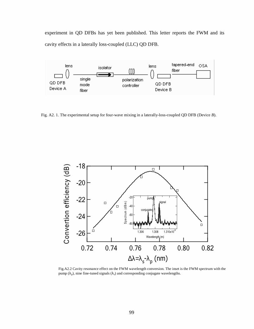
99
experiment in QD DFBs has yet been published. This letter reports the FWM and its
cavity effects in a laterally loss-coupled (LLC) QD DFB.
Fig. A2. 1. The experimental setup for four-wave mixing in a laterally-loss-coupled QD DFB (Device B).
&$ $22 ,
333333
∆λ=λλ
"
3"
33
#
$H
Fig.A2.2 Cavity resonance effect on the FWM wavelength conversion. The inset is the FWM spectrum with the pump (λp), nine fine-tuned signals (λs) and corresponding conjugate wavelengths.
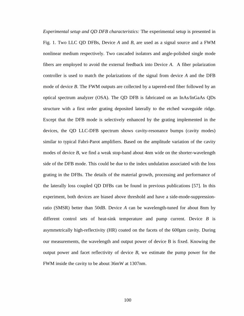
100
Experimental setup and QD DFB characteristics: The experimental setup is presented in
Fig. 1. Two LLC QD DFBs, Device A and B, are used as a signal source and a FWM
nonlinear medium respectively. Two cascaded isolators and angle-polished single mode
fibers are employed to avoid the external feedback into Device A. A fiber polarization
controller is used to match the polarizations of the signal from device A and the DFB
mode of device B. The FWM outputs are collected by a tapered-end fiber followed by an
optical spectrum analyzer (OSA). The QD DFB is fabricated on an InAs/InGaAs QDs
structure with a first order grating deposited laterally to the etched waveguide ridge.
Except that the DFB mode is selectively enhanced by the grating implemented in the
devices, the QD LLC-DFB spectrum shows cavity-resonance bumps (cavity modes)
similar to typical Fabri-Parot amplifiers. Based on the amplitude variation of the cavity
modes of device B, we find a weak stop-band about 4nm wide on the shorter-wavelength
side of the DFB mode. This could be due to the index undulation associated with the loss
grating in the DFBs. The details of the material growth, processing and performance of
the laterally loss coupled QD DFBs can be found in previous publications [57]. In this
experiment, both devices are biased above threshold and have a side-mode-suppression-
ratio (SMSR) better than 50dB. Device A can be wavelength-tuned for about 8nm by
different control sets of heat-sink temperature and pump current. Device B is
asymmetrically high-reflectivity (HR) coated on the facets of the 600µm cavity. During
our measurements, the wavelength and output power of device B is fixed. Knowing the
output power and facet reflectivity of device B, we estimate the pump power for the
FWM inside the cavity to be about 36mW at 1307nm.

101
Results and discussion: As shown in the inset of fig.2, a strong cavity effect on the
wavelength conversion is observed when we tune the signal wavelength around the
second cavity mode counted from the DFB mode. The conversion efficiency is plotted as
function of the detuning from the pump in fig.2 with a maximum at the wavelength of the
cavity mode. To estimate the 3dB bandwidth due to the cavity resonance, we curve-fit the
data to a Lorenztian function and the full width of the half maximum (FWHM) is found
to be 0.05 nm, corresponding to a conversion bandwidth about 9GHz at 1307nm.
We also investigate the FWM in device B over a wider spectrum range as shown in fig.3.
For each data point, the wavelength of signal is carefully tuned so that the FWM
conversion efficiency is maximized by lining up the conjugate beam with the cavity
resonances. The locally maximized conversion efficiency varies from -14 dB to -30 dB
with the detuning increases from 0.33 nm to 8nm, that is, from 60 GHz to 1.4 THz, with
an inside-cavity pump power fixed at 36mA in device B. These efficiencies are
comparable to the reported data in an index-coupled QW DFB with much higher carrier
density [126]. As the conversion efficiency is plotted in fig.4 in log scales, we find two
different regimes of the slope of the conversion efficiency relative to the signal-pump
detuning: for 0.3nm to 3.3nm the slope is about -1.2 while for 4nm to 8nm about -2.4.
Theoretically, the slope should close to -2 since |χ(3)|2 is a Lorentzian function of
frequency detuning. In our case, cavity resonance should be taken into account. Applying
the Haiki-Pioli technique [132] to the lasing spectrum of device B, we find that the net
round-trip gain, defined as r1r2exp(2gL) with g the gain, L the cavity length, r1 and r2 the
reflectivities of the facets, has a positive slope in the regime from 0.3nm to 3.3nm and a
negative one from 4nm to 8nm. Larger gain indicates a stronger cavity enhancement and

102
this explains the slope difference in fig.3. This non-constant distribution of the net gain in
the device is resultant from the stop-band (about 4nm wide as observed in lasing
spectrum) and also could from the spectrum hole burning effect which is believed to be
significant in QDs [79]. The discontinuation around 4nm could be attributed to the
crossing-over of the stop band.
Conclusion: The FWM in a quantum dot LLC DFB laser at 1307 nm is reported in this
paper. The conversion efficiency is found to change from -14dB to -30dB for a detuning
range from 60 GHz to 1.4 THz. The conversion efficiency is found proportional to (∆λ)-
1.2 in the detune range of 0.3nm to 3.3 nm while (∆λ)-2.4 of 4nm to 8nm, which can be
contributed to the cavity resonance and the net gain non-uniformity due to the residual
stop-band from the loss grating and probably the spectrum hole burning effect in the QD
DFB. Cavity enhancement of the wavelength conversion is characterized with a
bandwidth about 9GHz.

103
3"
333
µ
1*$
&$H
Fig. A2. 3. A plot of the DFB spectrum with twenty signals detuned differently from the pump wavelength. The FWM efficiency is maximized for each detuning by lining up the conjugate beam with the cavity mode.
&$# $22 ,
3
C$
Fig.A2. 4. The FWM conversion efficiency with maximum cavity enhancement versus the detuning in the spectrum presented in fig.3. The net round-trip gain is obtained from the DFB spectrum without FWM using Haiki-Pioli technique.

104
Appendix C. MATLAB CODE FOR THE THRESHOLD AND YIELD
CALCULATIONS OF DFBS
1. dispersion_relation.m
clear all; %Kfb=input('input Kfb: '); %Kbf=input('input Kbf: '); r1_facet=input('input r1: '); r2_facet=input('input r2: '); m=30; LL=50; JL=50; index1=1;index2=1; s_stat_index=0; options = optimset('Display','off'); % Turn off Display for Kfb=0.5:0.5:5 Kbf=-Kfb; %minus for index coupled, plus for gain coupled for k = 0:m Kbf k tic; for n = 0:m r1=r1_facet*(cos(pi*2.0*k/m)+i*sin(pi*2.0*k/m)); r2=r2_facet*(cos(pi*2.0*n/m)+i*sin(pi*2.0*n/m)); index1=1;index2=1; for L = 0:LL %pp=L for J = 0:JL p = (0.2*L)+(0.2*J-5)*i; if abs(threshold1(p,r1,r2,Kfb,Kbf))<1 if index1==1 SS1(1)=p; index1=2; else if abs(p-SS1(index1-1))>1 SS1(index1)=p; index1=index1+1; end end end if abs(threshold2(p,r1,r2,Kfb,Kbf))<1 if index2==1 SS2(1)=p; index2=2; else if abs(p-SS2(index2-1))>1 SS2(index2)=p; index2=index2+1; end end end

105
end end %index s1_index=1; for s_index = 1:(index1-1) [s_value,f_value] = fsolve(@threshold1,SS1(s_index),options,r1,r2,Kfb,Kbf); if (abs(f_value)<0.0001) if(s1_index==1) Solutions1(k+1,n+1,s1_index)=s_value; s1_index=s1_index+1; else for loop_filter=(1:s1_index-1) if(abs(s_value-Solutions1(k+1,n+1,s1_index-loop_filter))<0.01) solution_match=1; break; else solution_match=0; end end if(solution_match==0) Solutions1(k+1,n+1,s1_index)=s_value; s1_index=s1_index+1; end end end end for s_index=1:(s1_index-1) Solutions1(k+1,n+1,s_index)=sqrt(Solutions1(k+1,n+1,s_index)^2-Kfb*Kbf); Solutions1(k+1,n+1,s_index)=real(Solutions1(k+1,n+1,s_index))+2*i*imag(Solutions1(k+1,n+1,s_index)); if (imag(Solutions1(k+1,n+1,s_index))<0) Solutions1(k+1,n+1,s_index)=-Solutions1(k+1,n+1,s_index); end end %change the solution to Beta %Solutions1(k+1,n+1,s_index)=sqrt(Solutions1(k+1,n+1,s_index)^2-Kfb*Kbf); % the gain is doubled when considering the gain of amplitude %Solutions1(k+1,n+1,s_index)=real(Solutions1(k+1,n+1,s_index))+2*i*imag(Solutions1(k+1,n+1,s_index)); s2_index=1;f_value=1; for s_index = 1:(index2-1) [s_value,f_value] = fsolve(@threshold2,SS2(s_index),options,r1,r2,Kfb,Kbf); if (abs(f_value)<0.0001) if(s2_index==1) Solutions2(k+1,n+1,s2_index)=s_value; s2_index=s2_index+1; else for loop_filter=(1:s2_index-1) if(abs(s_value-Solutions2(k+1,n+1,s2_index-loop_filter))<0.01) solution_match=1; break; else solution_match=0; end end if(solution_match==0)

106
Solutions2(k+1,n+1,s2_index)=s_value; s2_index=s2_index+1; end end end end for s_index=1:(s2_index-1) Solutions2(k+1,n+1,s_index)=sqrt(Solutions2(k+1,n+1,s_index)^2-Kfb*Kbf); Solutions2(k+1,n+1,s_index)=real(Solutions2(k+1,n+1,s_index))+2*i*imag(Solutions2(k+1,n+1,s_index)); if (imag(Solutions2(k+1,n+1,s_index))<0) Solutions2(k+1,n+1,s_index)=-Solutions2(k+1,n+1,s_index); end end s_min_1(k+1,n+1)=1000*(1+i); s_min_2(k+1,n+1)=1000*(1+i); for s_index=1:s1_index-1 if(abs(Solutions1(k+1,n+1,s_index))<1e-5)|(abs(s_min_1(k+1,n+1)-Solutions1(k+1,n+1,s_index))<1e-4) break; end if(imag(s_min_1(k+1,n+1))>imag(Solutions1(k+1,n+1,s_index))) s_min_2(k+1,n+1)=s_min_1(k+1,n+1); s_min_1(k+1,n+1)=Solutions1(k+1,n+1,s_index); else if(imag(s_min_2(k+1,n+1))>imag(Solutions1(k+1,n+1,s_index))) s_min_2(k+1,n+1)=Solutions1(k+1,n+1,s_index); end end end for s_index=1:s2_index-1 if(abs(Solutions2(k+1,n+1,s_index))<1e-5)|(abs(s_min_1(k+1,n+1)-Solutions2(k+1,n+1,s_index))<1e-4) break; end if(imag(s_min_1(k+1,n+1))>imag(Solutions2(k+1,n+1,s_index))) s_min_2(k+1,n+1)=s_min_1(k+1,n+1); s_min_1(k+1,n+1)=Solutions2(k+1,n+1,s_index); else if(imag(s_min_2(k+1,n+1))>imag(Solutions2(k+1,n+1,s_index))) s_min_2(k+1,n+1)=Solutions2(k+1,n+1,s_index); end end end s_stat_index=s_stat_index+1; s_stat(s_stat_index)=imag(s_min_2(k+1,n+1)-s_min_1(k+1,n+1)); end toc end hold on; h=cdfplot(s_stat); newz = 1-get(h(1),'Ydata');
107
set(h(1),'Ydata',newz,'Color','red'); result_file=['yield_' 'Kfb' num2str(Kfb) '_Kbf' num2str(Kbf) '_r1_' num2str(abs(r1)) '_r2_' num2str(abs(r2)) '.mat'] save(result_file); end
2. threshold1.m function y = threshold1(x,r1,r2,Kfb,Kbf) y = F21(x,Kbf)*r1+F22(x,Kfb,Kbf)-r2*(F11(x,Kfb,Kbf)*r1+F12(x,Kfb)); function y = F11(x,Kfb,Kbf) y=cos(x)-i*sqrt(x^2-Kfb*Kbf)*sinc(x/pi); function y = F22(x,Kfb,Kbf) y=cos(x)+i*sqrt(x^2-Kfb*Kbf)*sinc(x/pi); function y = F12(x,Kfb) y=Kfb*sinc(x/pi); function y = F21(x,Kbf) y=-Kbf*sinc(x/pi);
3. threshold2.m function y = threshold2(x,r1,r2,Kfb,Kbf) y = F21(x,Kbf)*r1+F22(x,Kfb,Kbf)-r2*(F11(x,Kfb,Kbf)*r1+F12(x,Kfb)); function y = F11(x,Kfb,Kbf) y=cos(x)+i*sqrt(x^2-Kfb*Kbf)*sinc(x/pi); function y = F22(x,Kfb,Kbf) y=cos(x)-i*sqrt(x^2-Kfb*Kbf)*sinc(x/pi); function y = F12(x,Kfb) y=Kfb*sinc(x/pi); function y = F21(x,Kbf) y=-Kbf*sinc(x/pi);

108
Appendix D. HIGH GAIN QUANTUM DOT SEMICONDUCTOR
OPTICAL AMPLIFIER FOR 1300 NM
Abstract— Using an AlGaAs/GaAs waveguide structure with a six-stack
InAs/InGaAs DWELL gain region having an aggregate dot density of approximately
8 x 1011 cm-2, an optical gain of 18 dB at 1300 nm has been obtained in a 2.4-mm long
amplifier at 100-mA pump current. The optical bandwidth is 50 nm, and the output
saturation power is 9 dBm. The dependence of the amplifier parameters on the pump
current and the gain recovery dynamics has also been studied.
1. DEVICE STRUCTURE AND EXPERIMENT RESULTS
A six-stack InAs/InGaAs “dots-in-a-well” (DWELL) amplifier structure was grown
by solid source molecular beam epitaxy on a (001) GaAs substrate using conditions and
design criteria similar to those published previously [4,13]. The average dot density in a
layer is about 1.3 x 1011 cm-2. The amplifier was fabricated using tilted ridge waveguide
geometry. The 4-micron ridge was formed with inductively coupled plasma etching using
BCl3 to remove part of AlGaAs cladding. Self-alignment of the ridge was achieved by
protecting it with SiNx during a wet oxidation of the remaining AlGaAs cladding layer.
Ti/Pt/Au was evaporated for the metal contact to the p+-GaAs cap layer. The substrate
was lapped and polished to a thickness of 100 µm and AuGe/Ni/Au was deposited for the
n-type contact. The waveguide length is 2.4 mm. The cleaved facets with a tilt angle of
6.8° were left uncoated and provided a sufficiently low level of back reflection and thus
of spectral ripples. Since available lensed fibers were used for coupling without any

109
optimization, the coupling losses were quite high and all the parameters reported below
are given for the amplifier with these fiber-coupling losses de-embedded.
Electroluminescence measurements of the structure (Fig. D.1) show a ground state
peak at 1305 nm with a spectral FWHM of 65 nm, indicating good homogeneity of the
quantum dots. The origin of the ASE power decrease at currents above 100 mA is due to
heating from the parasitic series resistance. It is also possible that a gradual misalignment
of the collection optics with temperature could contribute to the decrease in measured
power. Nevertheless, the important point is that the position of the ground state does not
change appreciably with different pump levels. A possible explanation is that the thermal
red shift of the band gap is balanced by a carrier band-filling effect. The spectrum shape
doesn't change because it is determined primarily by dot inhomogeneity, which is
temperature independent and the excited state population is not significant. Because of
the saturation of the ground state energy levels at relatively low pump levels and the
resulting occupation of excited energy levels with higher state densities, the blue shift in
the QD emission due to band filling could be more significant than in a quantum well.
Similar behavior has also been observed in experiments with the QD-SOA chip. The
results obtained demonstrate the potential of QD technology for devices with high
temperature stability because blue-shifting and red-shifting can be balanced.
A typical spectrum of the ASE in the QD-SOA is presented in Fig. D.2. The ASE
maximum (disregarding spectral ripples) is at 1295 nm and the FWHM is 50 nm. The
different peak wavelengths and FWHM’s between the SOA and the electroluminescence
are probably due to material differences across the 2-inch wafer. The Fabry-Perot spectral
ripples at operating currents are quite low, < 2 dB, with their period of ~0.1 nm

110
corresponding to the chip length. It is noted that the slow amplitude modulation in the
ripple in Fig. D. 2 is an intrinsic chip feature and is not caused by interference effects
from the lensed fibers used for the coupling, because neither the position nor the
amplitude of the ripples are fiber tip position dependent. The slow ripple is most probably
due to wavelength dependent backreflection because of the mode conversion on the tilted
facet [133] and coupling with substrate modes due to the transparency of the GaAs wafer
substrate at 1300 nm [134]. The onset of lasing at 1304.5 nm ultimately limits the
maximum QD-SOA gain. This indicates that probably even higher gain and obviously
lower ripples could be obtained if the chip facets were AR-coated. In Fig. (D. 3) the ASE
spectra for no signal and in saturation are presented. For the case where a 1300-nm CW
signal is injected, it is seen that the spectral broadening is quasi-homogeneous in a wide
spectral range around the gain maximum. This conclusion is supported by the fact that
the reduction in the ASE power occurs in a broad wavelength region around the
saturating signal. Such a wide homogeneous bandwidth is rather usual for operation of
electrically pumped QD-SOA at room temperature when the dephasing time is very short
as discussed in Chapter one. In our case of CW operation the inhomogeneous broadening
due to dot size distribution is additionally masked by the carrier transport effects, which
play an essential role there as could be concluded from the fact that saturation of the ASE
power is significantly stronger on the red side than on the blue one.
The dependence of the QD-SOA chip small signal gain at wavelength 1300 nm on the
current is presented in Fig. (D.4). The gain was measured by comparing the device gain
to that at transparency current (~30 mA), which was determined by monitoring the
saturation of the device transmission at high power of input signal. As the waveguide

111
losses are low, <2 cm-1 it gives only a small, maximum 2 dB correction to the gain value.
The results show a good agreement with the on/off gain (~40 dB) and the values obtained
from the fiber-to-fiber gain minus the coupling losses (~12 dB per facet), which were
estimated by comparing the ASE power coupled in the fiber to the total ASE power. The
high loss value is mainly because spherical fiber tapers were used while the light beam
had 3:1 ellipticity. The coupling could be improved using, for example, biconic lensed
fiber tapers. At currents in the vicinity of the lasing threshold (135 mA) the gain reaches
the value of ~18 dB (17 cm-1), which is consistent the data on the ground state saturated
gain in a Fabry-Perot laser grown under similar conditions [135]. In QD lasers, gain
saturation is usually determined by the complete population of the quantum dot ground
state. However, as already mentioned heating could also cause the gain saturation effect
(Fig. D.1). The gain has strong, at least 20-dB polarization dependence. It is due to the
QD gain polarization dependence – the TM gain maximum is significantly blue shifted
either because the light-hole energy levels are not confined within the heavily
compressively strained QD or because of the particular shape of the dot. Only if the dot
had a symmetric cross-section in the direction of light propagation, the TE and TM
ground state gain would be equal. The problem of strong polarization-dependent gain
could be relaxed using a double pass with polarization rotation or polarization diversity
configurations. In Fig. D.4 the current dependence of the 3-dB gain saturation power
(chip output) for a CW signal at 1300 nm is also shown together with the typical
dependence of the QD-SOA gain on the output power. Values of ~9 dBm output
saturation power are achievable. It is comparable with that of common bulk- and MQW-
SOA’s but it is essentially lower than the values obtained in numerical simulations [30].

112
Due to the onset of the lasing and heating, strong inversion of the QD ground state and
the extremely low differential gain desirable for high saturation power could not be
reached. The carrier capture time was also about one order of magnitude longer than that
assumed in the simulations as it will be shown further. The linewidth enhancement factor
has been estimated by the shift of the ASE spectral ripples in gain saturation as illustrated
in Fig. D.5. As it is typical for QD devices, the linewidth enhancement factor is very low
- ~0.1. It is essentially lower than the typical value of ~5 for MQW-SOA, which was also
measured in the same set up for a common commercially available 1300-nm MQW-SOA.
From the ASE spectral density the noise figure of the QD-SOA was estimated to be
~8 dB taking into account that the ASE is polarized.
The gain recovery dynamics of the QD-SOA sample was also studied. The
measurements were based on the beating of two pulse trains with close pulse repetition
frequencies. A 1.25-GHz train of 12-ps pulses with the center wavelength of 1300 nm
served as the pump. The probe pulse train of 1.5-ps pulses at 1296 nm had 1.25 GHz-
125 Hz repetition frequency. The maximum temporal delay is set by the pulse repetition
frequency to ~800 ps. The QD-SOA gain dynamics for different currents is shown in
Fig. D.6 together with the results obtained for a common 1300-nm MWQ-SOA. In a
conventional MQW-SOA (Fig. D.6 b), for pulses longer than a few picoseconds the
relaxation dynamics can be well described by a single exponent and the recovery time is
strongly dependent on the carrier density. On the contrary, the recovery dynamics of the
QD-SOA gain can be characterized by two time constants. Those were found to be
1~9 ps
2~140 ps by fitting a double exponent to the logarithm of the gain recovery
profile. It is worth noting that the relaxation time constants were found to be practically

113
independent of the driving current in the studied range. The dependence of the relaxation
time constants on the input pulse energy was also studied. It was found that for up to
4 dB pulse gain saturation there are no pronounced changes in the gain recovery
dynamics.
The initial fast incomplete gain recovery with a relaxation time ~9 ps could be
attributed to several effects. On one side it could be an extensively discussed relaxation
bottle neck but usually the carrier relaxation time to the QD ground state is ~1 ps,
significantly shorter than the observed one. On the other side it could be an interdot
(“tunneling”) relaxation between the lateral coupled dots in a QD layer, which could
become possible for room temperature at high QD densities, when coupling can lower the
barrier between the QD [136,137]. The longer relaxation time constant corresponds to the
relaxation of the total carrier density. More detailed investigations, are necessary to
clarify the physics of the gain recovery dynamics. But it is out of the scope of the present
paper. Especially the second, total carrier density relaxation process with 140-ps time
would be an inhibiting factor for high bit rate transmission similar to the case of common
bulk and MQW-SOA. Probably the effect might be reduced by optimization of the
structure and especially by increasing the pump current [37]. In our case the maximum
pump current was limited by the onset of lasing.
2. CONCLUSIONS
Parameters of a 1300-nm quantum dot semiconductor optical amplifier built using a
2.4-mm long structure of six InAs/InGaAs DWELL layers with very high dot density
(8 x 1011 cm-2) have been studied. A gain as high as 18 dB with 50-nm bandwidth has
been reached at low current (100 mA). The output saturation power for a CW signal is

114
~9 dBm. The linewidth enhancement factor is below 0.1. The polarization dependence of
the gain is more than 20 dB, the noise figure is about 8 dB. Gain peak wavelength and
bandwidth are practically temperature independent.
The obtained parameters are better than or comparable to that of a common SOA. It
shows prospects of QD-SOA deployment in optical networks because of the ultra-fast
gain recovery and the low linewidth enhancement factor, which allow to decrease the
signal distortions by cross-gain modulation and chirp generation in high bit rate systems.

115
Fig. D.1. Electroluminescence spectra of the DWELL structure with the heat sink
temperature fixed at 18oC for different injection currents.
Fig. D.2. ASE spectrum of QD-SOA at the vicinity of the lasing threshold with a
magnification of the central part in the inset. Optical resolution bandwidth
is 0.01 nm.
-80
-70
-60
1500 1300 1100
Ground state
25mA
50mA 75mA
125mA
100mA P
ower
[dB
]
Wavelength [nm]
1250 1300 1350
-60
-54
-48
1296 1297 1298
-52,0
-51,5
Pow
er [d
B]
Wavelength [nm]

116
1250 1300 1350-70
-65
-60
-55
-50
0
1
2
3
4
Pow
er [d
B]
Wavelength [nm]
Sat
urat
ion
[dB
]
Fig. D.3. ASE spectra without and with a CW signal at 3-dB gain saturation and
their ratio. The signal peak is outside the plot area.
30 50 70 90 110 1300
5
10
15
20
0
5
10
15
20
Gai
n [d
B]
Current [mA]
Pow
er [d
Bm
]
(a)
2 4 6 814
15
16
17
18
Gai
n [d
B]
Power [dBm] (b)
Fig. D.4. The small signal gain and 3-dB saturation output power dependence on
current at 1300 nm (a); gain dependence on output power for 100-mA
pump current (b). Heat sink temperature was 24°C.

117
1307,0 1307,5
-69,0
-68,5
-71,0
-70,5
Pow
er [d
Bm
]
Wavelength [nm]
Fig. D.5. ASE spectral ripples without (upper curve) and with CW signal at 2-dB
gain saturation (bottom curve) in a QD-SOA ( H~0.1).
0 200 400 600 800 1000
0.5
1.0
130 mA
90 mA
100 mA
75 mA
Gai
n [a
.u.]
Time [ps] (a)
0 200 400 600 800 10000.0
1.0
400 mA300 mA250 mA200 mA
150 mA
100 mA
Gai
n [a
.u.]
Time [ps](b)
Fig. D.6. Gain recovery dynamics for the QD-SOA (a) and for a common MQW-
SOA (b) for different currents. Shift of curves corresponds to the change of
the small signal gain. The pump pulse duration: a) 12 ps and b) ~20 ps. The
input pump pulse energy: a) ~ 40 fJ; b) ~300 fJ.

118
BIBLIOGRAPHY
1. Y. ARAKAWA and H. SAKAKI, "MULTIDIMENSIONAL QUANTUM WELL LASER AND
TEMPERATURE-DEPENDENCE OF ITS THRESHOLD CURRENT," APPLIED PHYSICS LETTERS 40, 939-941.
2. N. KIRSTAEDTER, N. N. LEDENTSOV, M. GRUNDMANN, D. BIMBERG, V. M. USTINOV, S. S. RUVIMOV, M. V. MAXIMOV, P. S. KOPEV, Z. I. ALFEROV, U. RICHTER, P. WERNER, U. GOSELE, and J. HEYDENREICH, "LOW-THRESHOLD, LARGE T-O INJECTION-LASER EMISSION FROM (INGA)AS QUANTUM DOTS," ELECTRONICS LETTERS 30, 1416-1417.
3. N. N. LEDENTSOV, V. M. USTINOV, A. Y. EGOROV, A. E. ZHUKOV, M. V. MAKSIMOV, I. G. TABATADZE, and P. S. KOPEV, "OPTICAL-PROPERTIES OF HETEROSTRUCTURES WITH INGAAS-GAAS QUANTUM CLUSTERS," SEMICONDUCTORS 28, 832-834 (1994).
4. G. T. Liu, A. Stintz, H. Li, K. J. Malloy, and L. F. Lester, "Extremely low room-temperature threshold current density diode lasers using InAs dots in In0.15Ga0.85As quantum well," ELECTRONICS LETTERS 35, 1163-1165 (1999).
5. M. ASADA, Y. MIYAMOTO, and Y. SUEMATSU, "GAIN AND THE THRESHOLD OF 3-DIMENSIONAL QUANTUM-BOX LASERS," IEEE JOURNAL OF QUANTUM ELECTRONICS 22, 1915-1921 (1986).
6. O. B. Shchekin and D. G. Deppe, "1.3 mu m InAs quantum dot laser with T-o=161 K from 0 to 80 degrees C," APPLIED PHYSICS LETTERS 80, 3277-3279 (2002).
7. T. C. Newell, D. J. Bossert, A. Stintz, B. Fuchs, K. J. Malloy, and L. F. Lester, "Gain and linewidth enhancement factor in InAs quantum-dot laser diodes," IEEE PHOTONICS TECHNOLOGY LETTERS 11, 1527-1529 (1999).
8. N. A. Sobolev, A. Cavaco, M. C. Carmo, M. Grundmann, F. Heinrichsdorff, and D. Bimberg, "Enhanced radiation hardness of InAs/GaAs quantum dot structures," Physica Status Solidi B-Basic Research 224, 93-96 (2001).
9. F. Guffarth, R. Heitz, M. Geller, C. Kapteyn, H. Born, R. Sellin, A. Hoffmann, D. Bimberg, N. A. Sobolev, and M. C. Carmo, "Radiation hardness of InGaAs/GaAs quantum dots," APPLIED PHYSICS LETTERS 82, 1941-1943 (2003).
10. Z. Alferov, "Double heterostructure lasers: Early days and future perspectives," IEEE JOURNAL OF SELECTED TOPICS IN QUANTUM ELECTRONICS 6, 832-840 (2000).
11. Bimberg, D. High power single and multimode quantum dot lasers with superior beam profile. Phtonics West section 5365[2004.]. 1-26-2004.
12. L. A. Coldren and S. W. Corzine, Diode lasers and photonic integrated circuits, (John Wiley & Sons, Inc., 1995).
13. G. T. Liu, A. Stintz, H. Li, T. C. Newell, A. L. Gray, P. M. Varangis, K. J. Malloy, and L. F. Lester, "The influence of quantum-well composition on the performance of quantum dot lasers using InAs/InGaAs dots-in-a-well (DWELL) structures," IEEE JOURNAL OF QUANTUM ELECTRONICS 36, 1272-1279 (2000).

119
14. N. Kirstaedter, O. G. Schmidt, N. N. Ledentsov, D. Bimberg, V. M. Ustinov, A. Y. Egorov, A. E. Zhukov, M. V. Maximov, P. S. KOPEV, and Z. I. Alferov, "Gain and differential gain of single layer InAs/GaAs quantum dot injection lasers," APPLIED PHYSICS LETTERS 69, 1226-1228 (1996).
15. K. Kamath, J. Phillips, H. Jiang, J. Singh, and P. Bhattacharya, "Small-signal modulation and differential gain of single-mode self-organized In0.4Ga0.6As/GaAs quantum dot lasers," APPLIED PHYSICS LETTERS 70, 2952-2953 (1997).
16. A. A. Ukhanov, "Study of the Carrier-induced optical properties in III-V quantum confined laser nano-structures," 2004).
17. N. Kirstaedter, N. N. Ledentsov, M. Grundmann, D. Bimberg, V. M. Ustinov, S. S. RUVIMOV, M. V. Maximov, P. S. KOPEV, Z. I. Alferov, U. RICHTER, P. Werner, U. Gosele, and J. HEYDENREICH, "LOW-THRESHOLD, LARGE T-O INJECTION-LASER EMISSION FROM (INGA)AS QUANTUM DOTS," ELECTRONICS LETTERS 30, 1416-1417 (1994).
18. K. Mukai, Y. Nakata, K. Otsubo, M. Sugawara, N. Yokoyama, and H. Ishikawa, "High characteristic temperature of near-1.3-mu m InGaAs/GaAs quantum-dot lasers at room temperature," APPLIED PHYSICS LETTERS 76, 3349-3351.
19. O. B. Shchekin and D. G. Deppe, "Low-threshold high-T-O 1.3-mu m InAs quantum-dot lasers due to P-type modulation doping of the active region," IEEE PHOTONICS TECHNOLOGY LETTERS 14, 1231-1233 (2002).
20. D. Bimberg and N. Ledentsov, "Quantum dots: lasers and amplifiers," JOURNAL OF PHYSICS-CONDENSED MATTER 15, R1063-R1076 (2003).
21. K. Mukai, Y. Nakata, K. Otsubo, M. Sugawara, N. Yokoyama, and H. Ishikawa, "High characteristic temperature of near-1.3-mu m InGaAs/GaAs quantum-dot lasers at room temperature," APPLIED PHYSICS LETTERS 76, 3349-3351.
22. L. V. Asryan and R. A. Suris, "Characteristic temperature of quantum dot laser," ELECTRONICS LETTERS 33, 1871-1872.
23. P. M. Smowton, E. J. Pearce, H. C. Schneider, W. W. Chow, and M. Hopkinson, "Filamentation and linewidth enhancement factor in InGaAs quantum dot lasers," APPLIED PHYSICS LETTERS 81, 3251-3253 (2003).
24. A. V. Uskov, E. P. O'Reilly, D. McPeake, N. N. Ledentsov, D. Bimberg, and G. Huyet, "Carrier-induced refractive index in quantum dot structures due to transitions from discrete quantum dot levels to continuum states," APPLIED PHYSICS LETTERS 84, 272-274 (2004).
25. A. V. Uskov, E. P. O'Reilly, D. McPeake, N. N. Ledentsov, D. Bimberg, and G. Huyet, "Carrier-induced refractive index in quantum dot structures due to transitions from discrete quantum dot levels to continuum states," APPLIED PHYSICS LETTERS 84, 272-274 (2004).
26. P. K. Kondratko, S. L. Chuang, G. Walter, T. Chung, and N. Holonyak, "Observations of near-zero linewidth enhancement factor in a quantum-well coupled quantum-dot laser," APPLIED PHYSICS LETTERS 83, 4818-4820 (2003).
27. S. Fathpour, P. Bhattacharya, S. Pradhan, and S. Ghosh, "Linewidth enhancement factor and near-field pattern in tunnel injection In0.4Ga0.6As self-assembled quantum dot lasers," ELECTRONICS LETTERS 39, 1443-1445 (2003).

120
28. Leo H.Spiekman, "Semiconductor Optical Amplifier," Optical Fiber Telecommunications, (Elsevier Science, 2002), 699-732.
29. O. Qasaimeh, "Optical gain and saturation characteristics of quantum-dot semiconductor optical amplifiers," IEEE JOURNAL OF QUANTUM ELECTRONICS 39, 793-798 (2003).
30. T. W. Berg and J. Mork, "Quantum dot amplifiers with high output power and low noise," APPLIED PHYSICS LETTERS 82, 3083-3085 (2003).
31. T.Akiyama, M. Ekawa M. Sugawara H. Sudo K. Kawaguchi A. Kuramata H. Ebe K. Morito H. Imai and Y. Arakawa. An Ultrawide-Band (120 nm) Semiconductor Optical Amplifier Having an Extremely-High Penalty-Free Output Power of 23 dBm Realized with Quantum-Dot Active Layers. ECOC. 2003. 2003.
32. E. U. Rafailov, P. Loza-Alvarez, W. Sibbett, G. S. Sokolovskii, D. A. Livshits, A. E. Zhukov, and V. M. Ustinov, "Amplification of femtosecond pulses over by 18 dB in a quantum-dot semiconductor optical amplifier," IEEE PHOTONICS TECHNOLOGY LETTERS 15, 1023-1025 (2003).
33. Z. Bakonyi, H. Su, G. Onishchukov, L. F. Lester, A. L. Gray, T. C. Newell, and A. Tunnermann, "High-gain quantum-dot semiconductor optical amplifier for 1300 nm," IEEE JOURNAL OF QUANTUM ELECTRONICS 39, 1409-1414 (2003).
34. M. Sugawara, N. Hatori, T. Akiyama, Y. Nakata, and H. Ishikawa, "Quantum-dot semiconductor optical amplifiers for high bit-rate signal processing over 40 Gbit/s," JAPANESE JOURNAL OF APPLIED PHYSICS PART 2-LETTERS 40, L488-L491 (2001).
35. M. Sugawara, T. Akiyama, N. Hatori, Y. Nakata, H. Ebe, and H. Ishikawa, "Quantum-dot semiconductor optical amplifiers for high-bit-rate signal processing up to 160 Gb s(-1) and a new scheme of 3R regenerators," MEASUREMENT SCIENCE & TECHNOLOGY 13, 1683-1691 (2002).
36. T. Akiyama, H. Kuwatsuka, T. Simoyama, Y. Nakata, K. Mukai, M. Sugawara, O. Wada, and H. Ishikawa, "Nonlinear gain dynamics in quantum-dot optical amplifiers and its application to optical communication devices," IEEE JOURNAL OF QUANTUM ELECTRONICS 37, 1059-1065 (2001).
37. T. Akiyama, N. Hatori, Y. Nakata, H. Ebe, and M. Sugawara, "Pattern-effect-free semiconductor optical amplifier achieved using quantum dots," ELECTRONICS LETTERS 38, 1139-1140 (2002).
38. T. Akiyama, N. Hatori, Y. Nakata, H. Ebe, and M. Sugawara, "Pattern-effect-free amplification and cross-gain modulation achieved by using ultrafast gain nonlinearity in quantum-dot semiconductor optical amplifiers," PHYSICA STATUS SOLIDI B-BASIC RESEARCH 238, 301-304 (2003).
39. A. V. Uskov, T. W. Berg, and J. Mork, "Theory of pulse-train amplification without patterning effects in quantum-dot semiconductor optical amplifiers," IEEE JOURNAL OF QUANTUM ELECTRONICS 40, 306-320 (2004).
40. T. Akiyama, N. Hatori, Y. Nakata, H. Ebe, and M. Sugawara, "Pattern-effect-free amplification and cross-gain modulation achieved by using ultrafast gain nonlinearity in quantum-dot semiconductor optical amplifiers," PHYSICA STATUS SOLIDI B-BASIC RESEARCH 238, 301-304 (2003).

121
41. A. Bilenca, R. Alizon, V. Mikhelashhvili, D. Dahan, G. Eisenstein, R. Schwertberger, D. Gold, J. P. Reithmaier, and A. FORCHEL, "Broad-band wavelength conversion based on cross-gain modulation and four-wave mixing in InAs-InP quantum-dash semiconductor optical amplifiers operating at 1550 nm," IEEE PHOTONICS TECHNOLOGY LETTERS 15, 563-565 (2003).
42. O. Qasaimeh, "Characteristics of cross-gain (XG) wavelength conversion in quantum dot semiconductor optical amplifiers," IEEE PHOTONICS TECHNOLOGY LETTERS 16, 542-544 (2004).
43. T. Akiyama, O. Wada, H. Kuwatsuka, T. Simoyama, Y. Nakata, K. Mukai, M. Sugawara, and H. Ishikawa, "Nonlinear processes responsible for nondegenerate four-wave mixing in quantum-dot optical amplifiers," APPLIED PHYSICS LETTERS 77, 1753-1755 (2000).
44. T. Akiyama, H. Kuwatsuka, N. Hatori, Y. Nakata, H. Ebe, and M. Sugawara, "Symmetric highly efficient (similar to 0 dB) wavelength conversion based on four-wave mixing in quantum dot optical amplifiers," IEEE PHOTONICS TECHNOLOGY LETTERS 14, 1139-1141 (2002).
45. T. Akiyama, O. Wada, H. Kuwatsuka, T. Simoyama, Y. Nakata, K. Mukai, M. Sugawara, and H. Ishikawa, "Nonlinear processes responsible for nondegenerate four-wave mixing in quantum-dot optical amplifiers," APPLIED PHYSICS LETTERS 77, 1753-1755 (2000).
46. P. Borri, W. Langbein, J. M. Hvam, F. Heinrichsdorff, M. H. Mao, and D. Bimberg, "Time-resolved four-wave mixing in InAs/InGaAs quantum-dot amplifiers under electrical injection," APPLIED PHYSICS LETTERS 76, 1380-1382 (2000).
47. T. Akiyama, H. Kuwatsuka, T. Simoyama, Y. Nakata, K. Mukai, M. Sugawara, O. Wada, and H. Ishikawa, "Ultrafast nonlinear processes in quantum-dot optical amplifiers," OPTICAL AND QUANTUM ELECTRONICS 33, 927-938 (2001).
48. Bimberg, D. High power single and multimode quantum dot lasers with superior beam profile. Phtonics West section 5365[2004.]. 1-26-2004.
49. P. M. Varangis, H. Li, G. T. Liu, T. C. Newell, A. Stintz, B. Fuchs, K. J. Malloy, and L. F. Lester, "Low-threshold quantum dot lasers with 201 nm tuning range," ELECTRONICS LETTERS 36, 1544-1545 (2000).
50. H. Li, G. T. Liu, P. M. Varangis, T. C. Newell, A. Stintz, B. Fuchs, K. J. Malloy, and L. F. Lester, "150-nm tuning range in a grating-coupled external cavity quantum-dot laser," IEEE PHOTONICS TECHNOLOGY LETTERS 12, 759-761 (2000).
51. X. D. Huang, A. Stintz, H. Li, L. F. Lester, J. Cheng, and K. J. Malloy, "Passive mode-locking in 1.3 mu m two-section InAs quantum dot lasers," APPLIED PHYSICS LETTERS 78, 2825-2827 (2001).
52. M. Kamp, M. Schmitt, J. Hofmann, F. Schafer, J. P. Reithmaier, and A. FORCHEL, "InGaAs/AlGaAs quantum dot DFB lasers operating up to 213 degrees C," ELECTRONICS LETTERS 35, 2036-2037 (1999).
53. F. Klopf, R. Krebs, A. Wolf, M. Emmerling, J. P. Reithmaier, and A. FORCHEL, "InAs/GaInAs quantum dot DFB lasers emitting at 1.3 mu m," ELECTRONICS LETTERS 37, 634-636 (2001).
54. R. Krebs, F. Klopf, S. Rennon, J. P. Reithmaier, and A. FORCHEL, "High frequency characteristics of InAs/GaInAs quantum dot distributed feedback lasers emitting at 1.3 mu m," ELECTRONICS LETTERS 37, 1223-1225 (2001).

122
55. L.Zhang, R.Wang, Z.Zou, T.Newell, D.Webb, P.Varangis, and L.Lester. InAs quantum dot DFB lasers on GaAs for uncooled 1310nm fiber communications. Optical Fiber Communication Conference, Atlanta, GA. 2003.
56. H.Su, L. Zhang A. L. Gray R. Wang T. C. Newell and L. F. Lester. Linewidth study of GaAs-
InGaAs Quantum Dot Distributed Feedback Lasers. IEEE PHOTONICS TECHNOLOGY LETTERS , accepted. 2004.
57. H. Su, L. Zhang, A. L. Gray, R. Wang, T. C. Newell, K. J. Malloy, and L. F. Lester, "High
external feedback resistance of laterally loss-coupled distributed feedback quantum dot semiconductor lasers," IEEE PHOTONICS TECHNOLOGY LETTERS 15, 1504-1506 (2003).
58. M. Sugawara, K. Mukai, and H. Shoji, "Effect of phonon bottleneck on quantum-dot laser performance," Applied Physics Letters 71, 2791-2793 (1997).
59. M. Grundmann, R. Heitz, and D. Bimberg, "New approach to modeling carrier distribution in quantum dot ensembles: Gain and threshold of QD lasers and impact of phonon bottleneck," Physica E 2, 725-728 (1998).
60. X. Q. Li, H. Nakayama, and Y. Arakawa, "Lifetime of confined LO phonons in quantum dots and its impact on phonon bottleneck issue," Japanese Journal of Applied Physics Part 1-Regular Papers Short Notes & Review Papers 38, 473-476 (1999).
61. K. Mukai and M. Sugawara, "Slow carrier relaxation among sublevels in annealed self-formed InGaAs/GaAs quantum dots," Japanese Journal of Applied Physics Part 1-Regular Papers Short Notes & Review Papers 37, 5451-5456 (1998).
62. H. Tsuchiya and T. Miyoshi, "Influence of phonon bottleneck on a quantum dot laser," Solid-State Electronics 42, 1443-1447 (1998).
63. K. Ikeda, H. Sekiguchi, F. Minami, J. Yoshino, Y. Mitsumori, H. Amanai, S. Nagao, and S. Sakaki, "Phonon bottleneck effects in InAs/GaInP quantum dots," Journal of Luminescence 108, 273-276 (2004).
64. J. Urayama, T. B. Norris, J. Singh, and P. Bhattacharya, "Observation of phonon bottleneck in quantum dot electronic relaxation," PHYSICAL REVIEW LETTERS 86, 4930-4933 (2001).
65. T. S. Sosnowski, T. B. Norris, H. Jiang, J. Singh, K. Kamath, and P. Bhattacharya, "Rapid carrier relaxation in In0.4Ga0.6As/GaAs quantum dots characterized by differential transmission spectroscopy," PHYSICAL REVIEW B-CONDENSED MATTER 57, R9423-R9426 (1998).
66. S. Ghosh, P. Bhattacharya, E. Stoner, J. Singh, H. Jiang, S. Nuttinck, and J. Laskar, "Temperature-dependent measurement of Auger recombination in self-organized In0.4Ga0.6As/GaAs quantum dots," APPLIED PHYSICS LETTERS 79, 722-724 (2001).
67. I. P. Marko, A. D. Andreev, A. R. Adams, R. Krebs, J. P. Reithmaier, and A. FORCHEL, "Importance of Auger recombination in InAs 1.3 mu m quantum dot lasers," ELECTRONICS LETTERS 39, 58-59 (2003).
68. X. Q. Li, H. Nakayama, and Y. Arakawa, "Phonon bottleneck in quantum dots: Role of lifetime of the confined optical phonons," PHYSICAL REVIEW B-CONDENSED MATTER 59, 5069-5073 (1999).
69. P. Borri, S. Schneider, W. Langbein, U. Woggon, A. E. Zhukov, V. M. Ustinov, N. N. Ledentsov, Z. I. Alferov, D. Ouyang, and D. Bimberg, "Ultrafast carrier dynamics and dephasing in InAs

123
quantum-dot amplifiers emitting near 1.3-mu m-wavelength at room temperature," APPLIED PHYSICS LETTERS 79, 2633-2635 (2001).
70. P. Eliseev, H. Li, A. Stintz, G. T. Liu, T. C. Newell, K. J. Malloy, and L. F. Lester, "Tunable grating-coupled laser oscillation and spectral hole burning in an InAs quantum-dot laser diode," IEEE JOURNAL OF QUANTUM ELECTRONICS 36, 479-485 (2000).
71. D. GAMMON, S. RUDIN, T. L. REINECKE, D. S. KATZER, and C. S. KYONO, "PHONON BROADENING OF EXCITONS IN GAAS/ALXGA1-XAS QUANTUM-WELLS," PHYSICAL REVIEW B-CONDENSED MATTER 51, 16785-16789 (1995).
72. P. Borri, W. Langbein, J. M. Hvam, E. Heinrichsdorff, M. H. Mao, and D. Bimberg, "Ultrafast gain dynamics in InAs-InGaAs quantum-dot amplifiers," IEEE PHOTONICS TECHNOLOGY LETTERS 12, 594-596 (2000).
73. K. Kim, J. Urayama, T. B. Norris, J. Singh, J. Phillips, and P. Bhattacharya, "Gain dynamics and ultrafast spectral hole burning in In(Ga)As self-organized quantum dots," APPLIED PHYSICS LETTERS 81, 670-672 (2002).
74. D. A. Yarotski, R. D. Averitt, N. Negre, S. A. Crooker, A. J. Taylor, G. P. Donati, A. Stintz, L. F. Lester, and K. J. Malloy, "Ultrafast carrier-relaxation dynamics in self-assembled InAs/GaAs quantum dots," JOURNAL OF THE OPTICAL SOCIETY OF AMERICA B-OPTICAL PHYSICS 19, 1480-1484 (2002).
75. P. Borri, W. Langbein, J. M. Hvam, F. Heinrichsdorff, M. H. Mao, and D. Bimberg, "Spectral hole-burning and carrier-heating dynamics in quantum-dot amplifiers: Comparison with bulk amplifiers," PHYSICA STATUS SOLIDI B-BASIC RESEARCH 224, 419-423 (2001).
76. M. Sugawara, T. Akiyama, N. Hatori, Y. Nakata, H. Ebe, and H. Ishikawa, "Quantum-dot semiconductor optical amplifiers for high-bit-rate signal processing up to 160 Gb s(-1) and a new scheme of 3R regenerators," MEASUREMENT SCIENCE & TECHNOLOGY 13, 1683-1691 (2002).
77. G. P. AGRAWAL, "SPECTRAL HOLE-BURNING AND GAIN SATURATION IN SEMICONDUCTOR-LASERS - STRONG-SIGNAL THEORY," Journal of Applied Physics 63, 1232-1234 (1988).
78. T. Akiyama, H. Kuwatsuka, T. Simoyama, Y. Nakata, K. Mukai, M. Sugawara, O. Wada, and H. Ishikawa, "Ultrafast nonlinear processes in quantum-dot optical amplifiers," OPTICAL AND QUANTUM ELECTRONICS 33, 927-938 (2001).
79. M. Sugawara, T. Akiyama, N. Hatori, Y. Nakata, H. Ebe, and H. Ishikawa, "Quantum-dot semiconductor optical amplifiers for high-bit-rate signal processing up to 160 Gb s(-1) and a new scheme of 3R regenerators," MEASUREMENT SCIENCE & TECHNOLOGY 13, 1683-1691 (2002).
80. T. Akiyama, N. Hatori, Y. Nakata, H. Ebe, and M. Sugawara, "Pattern-effect-free semiconductor optical amplifier achieved using quantum dots," ELECTRONICS LETTERS 38, 1139-1140 (2002).
81. A. V. Uskov, E. P. O'Reilly, D. McPeake, N. N. Ledentsov, D. Bimberg, and G. Huyet, "Carrier-induced refractive index in quantum dot structures due to transitions from discrete quantum dot levels to continuum states," APPLIED PHYSICS LETTERS 84, 272-274 (2004).
82. P. Borri, W. Langbein, J. Mork, J. M. Hvam, F. Heinrichsdorff, M. H. Mao, and D. Bimberg, "Dephasing in InAs/GaAs quantum dots," PHYSICAL REVIEW B 60, 7784-7787 (1999).
124
83. A. Stintz, G. T. Liu, A. L. Gray, R. Spillers, S. M. Delgado, and K. J. Malloy, "Characterization of InAs quantum dots in strained InxGa1-xAs quantum wells," JOURNAL OF VACUUM SCIENCE & TECHNOLOGY B 18, 1496-1501 (2000).
84. M. Kamp, J. Hofmann, F. Schafer, M. Reinhard, M. Fischer, T. Bleuel, J. P. Reithmaier, and A. FORCHEL, "Lateral coupling - a material independent way to complex coupled DFB lasers," OPTICAL MATERIALS 17, 19-25 (2001).
85. P. Bhattacharya, D. Klotzkin, O. Qasaimeh, W. D. Zhou, S. Krishna, and D. H. Zhu, "High-speed modulation and switching characteristics of In(Ga)As-Al(Ga)As self-organized quantum-dot lasers," IEEE JOURNAL OF SELECTED TOPICS IN QUANTUM ELECTRONICS 6, 426-438 (2000).
86. D. Bimberg, N. Kirstaedter, N. N. Ledentsov, Z. I. Alferov, P. S. KOPEV, and V. M. Ustinov, "InGaAs-GaAs quantum-dot lasers," IEEE JOURNAL OF SELECTED TOPICS IN QUANTUM ELECTRONICS 3, 196-205 (1997).
87. L.A.Coldren and S.W.Corzine, Diode lasers and Photonics Integrated Circuits, (John Wiley & Sons, INC., 1995).
88. M. W. FLEMING and A. MOORADIAN, "SPECTRAL CHARACTERISTICS OF EXTERNAL-CAVITY CONTROLLED SEMICONDUCTOR-LASERS," IEEE Journal of Quantum Electronics 17, 44-59 (1981).
89. M. R. MATTHEWS, K. H. CAMERON, R. WYATT, and W. J. DEVLIN, "PACKAGED FREQUENCY-STABLE TUNABLE 20 KHZ LINEWIDTH 1.5-MU-M INGAASP EXTERNAL CAVITY LASER," Electronics Letters 21, 113-115 (1985).
90. E. PATZAK, A. SUGIMURA, S. SAITO, T. MUKAI, and H. OLESEN, "SEMICONDUCTOR-LASER LINEWIDTH IN OPTICAL FEEDBACK CONFIGURATIONS," Electronics Letters 19, 1026-1027 (1983).
91. M. OKAI, "SPECTRAL CHARACTERISTICS OF DISTRIBUTED-FEEDBACK SEMICONDUCTOR-LASERS AND THEIR IMPROVEMENTS BY CORRUGATION-PITCH-MODULATED STRUCTURE," Journal of Applied Physics 75, 1-29 (1994).
92. M. OKAI, M. SUZUKI, T. TANIWATARI, and N. CHINONE, "CORRUGATION-PITCH-MODULATED DISTRIBUTED-FEEDBACK LASERS WITH ULTRANARROW SPECTRAL LINEWIDTH," Japanese Journal of Applied Physics Part 1-Regular Papers Short Notes & Review Papers 33, 2563-2570 (1994).
93. S. TAKANO, T. SASAKI, H. YAMADA, M. KITAMURA, and I. MITO, "SUB-MHZ SPECTRAL LINEWIDTH IN 1.5-MU-M SEPARATE-CONFINEMENT-HETEROSTRUCTURE (SCH) QUANTUM-WELL DFB LDS," Electronics Letters 25, 356-357 (1989).
94. G.P.Agrawal, "Coherent Lightwave Systems," Fiber-Optic communication systems, (Wiley Interscience, 2002), 478-512.
95. H. OLESEN, B. TROMBORG, H. E. LASSEN, and X. PAN, "MODE-INSTABILITY AND LINEWIDTH REBROADENING IN DFB LASERS," Electronics Letters 28, 444-446 (1992).
96. X. PAN, B. TROMBORG, and H. OLESEN, "LINEWIDTH REBROADENING IN DFB LASERS DUE TO WEAK SIDE MODES," IEEE Photonics Technology Letters 3, 112-114 (1991).

125
97. H. WENZEL, H. J. WUNSCHE, and U. BANDELOW, "LINEWIDTH REBROADENING IN SEMICONDUCTOR-LASERS DUE TO LATERAL SPATIAL HOLEBURNING," Electronics Letters 27, 2301-2302 (1991).
98. G. P. AGRAWAL, G. H. DUAN, and P. GALLION, "INFLUENCE OF REFRACTIVE-INDEX NONLINEARITIES ON MODULATION AND NOISE PROPERTIES OF SEMICONDUCTOR-LASERS," Electronics Letters 28, 1773-1774 (1992).
99. F. Girardin, G. H. DUAN, and P. GALLION, "Linewidth rebroadening due to nonlinear gain and index induced by carrier heating in strained quantum-well lasers," IEEE Photonics Technology Letters 8, 334-336 (1996).
100. T. OKOSHI, K. KIKUCHI, and A. NAKAYAMA, "NOVEL METHOD FOR HIGH-RESOLUTION MEASUREMENT OF LASER OUTPUT SPECTRUM," Electronics Letters 16, 630-631 (1980).
101. Bin Zhao and Ammon Yariv, "Quantum well semiconductor lasers," Semiconductor lasers I Fundamenals, Eli Kapon, ed., (Academic press, 1999), 1-109.
102. K. PETERMANN, "EXTERNAL OPTICAL FEEDBACK PHENOMENA IN SEMICONDUCTOR-LASERS," IEEE Journal of Selected Topics in Quantum Electronics 1, 480-489 (1995).
103. M. F. Alam and M. A. Karim, "External optical feedback effects in distributed feedback semiconductor lasers," Advances in Imaging and Electron Physics, Vol 107 107, 73-120 (1999).
104. T. OKOSHI, K. KIKUCHI, and A. NAKAYAMA, "NOVEL METHOD FOR HIGH-RESOLUTION MEASUREMENT OF LASER OUTPUT SPECTRUM," Electronics Letters 16, 630-631 (1980).
105. K. H. Park, J. K. Lee, J. H. Han, H. S. Cho, D. H. Jang, C. S. Park, K. E. Pyun, and J. Jeong, "The effects of external optical feedback on the power penalty of DFB-LD modules for 2.5 Gb s(-1) optical transmission systems," Optical and Quantum Electronics 30, 23-31 (1998).
106. G.P.Agrawal, Fiber-Optic communication systems, (John Wiley and Sons Inc, 1997).
107. K. Inoue, "An experimental study on chirp noise in a directly modulated semiconductor laser," Ieice Transactions On Communications E81B, 1197-1202 (1998).
108. J. FENG, T. R. CHEN, and A. YARIV, "ON CHIRP CONTROL IN 2 SECTION DISTRIBUTED-FEEDBACK SEMICONDUCTOR-LASERS," Applied Physics Letters 67, 2913-2915 (1995).
109. C. Y. Tsai and C. Y. Tsai, "Effects of carrier heating on the frequency chirping of semiconductor lasers," Electronics Letters 33, 2043-2045 (1997).
110. M. Bhattacharya, R. Mukherjee, and T. Chattopadhyay, "Reduction of frequency chirping in semiconductor lasers through injection locking," Iete Journal of Research 45, 341-344 (1999).
111. R. Vinzio, Z. Toffano, and A. Destrez, "Analytical formulation of distortion and chirp in CATV DFB lasers including spatial hole burning," IEEE Journal of Quantum Electronics 34, 311-317 (1998).

126
112. G. E. Shtengel, R. F. Kazarinov, G. L. Belenky, and C. L. Reynolds, "Wavelength chirp and dependence of carrier temperature on current in MQW InGaAsP-InP lasers," IEEE Journal of Quantum Electronics 33, 1396-1402 (1997).
113. H. Saito, K. Nishi, A. Kamei, and S. Sugou, "Low chirp observed in directly modulated quantum dot lasers," IEEE PHOTONICS TECHNOLOGY LETTERS 12, 1298-1300 (2000).
114. H. Saito, K. Nishi, and S. Sugou, "Low chirp operation in 1.6 mu m quantum dot laser under 2.5 GHz direct modulation," ELECTRONICS LETTERS 37, 1293-1295 (2001).
115. K.Petermann, Laser diode modulation and noise, (Kluwer Academic Publishers, 1991).
116. Agilent Technologies. Making Time-Resolved Chirp Measurements using the optical spectrum analyzer and digital communication analyzer. 2004. Application Note 1550-7.
117. H. Li, "RF-modulation measurement of linewidth enhancement factor and nonlinear gain of
vertical-cavity surface-emitting lasers," IEEE Photonics Technology Letters 8, 1594-1596 (1996).
118. L.A.Coldren and S.W.Corzine, Diode lasers and Photonics Integrated Circuits, (John Wiley & Sons, INC., 1995), 213-221.
119. N. S. BERGANO, "WAVELENGTH DISCRIMINATOR METHOD FOR MEASURING DYNAMIC CHIRP IN DFB LASERS," Electronics Letters 24, 1296-1297 (1988).
120. Dougla M.Baney and Wayne V.Sorin, "high resolution optical frequency analysis," Fiber optic test and measurement, Dennis Derickson, ed., (Prentice Hall, 1998), 206-207.
121. Agilent Technologies. Making Time-Resolved Chirp Measurements using the optical spectrum analyzer and digital communication analyzer. 2002. Application Note 1550-7.
122. L.A.Coldren and S.W.Corzine, Diode lasers and Photonics Integrated Circuits, (John Wiley &
Sons, INC., 1995), 213-221.
123. Radhakrishnan Nagarajan and John E.Bowers, "High-speed Lasers," Semiconductor lasers I Fundamenals, Eli Kapon, ed., (Academic press, 1999), 177-290.
124. G.P.Agrawal, Fiber-Optic communication systems, (John Wiley & Sons, Inc., 2002).
125. J. Minch and S. L. Chuang, "Dual-pump four-wave mixing in a double-mode distributed feedback laser," JOURNAL OF THE OPTICAL SOCIETY OF AMERICA B-OPTICAL PHYSICS 17, 53-62 (2000).
126. H. Kuwatsuka, H. Shoji, M. Matsuda, and H. Ishikawa, "Nondegenerate four-wave mixing in a long-cavity lambda/4-shifted DFB laser using its lasing beam as pump beams," IEEE JOURNAL OF QUANTUM ELECTRONICS 33, 2002-2010 (1997).
127. J. R. Minch, C. S. Chang, and S. L. Chuang, "Wavelength conversion in distributed-feedback lasers," IEEE JOURNAL OF SELECTED TOPICS IN QUANTUM ELECTRONICS 3, 569-576 (1997).
128. I. Tomkos, I. Zacharopoulos, E. Roditi, and D. Syvridis, "Experimental investigation of wavelength conversion based on four-wave mixing in a three-electrode distributed feedback laser," APPLIED PHYSICS LETTERS 75, 1195-1197 (1999).

127
129. H. Ishikawa, "Applications of quantum dot to optical devices," SELF-ASSEMBLED INGAAS/GAAS QUANTUM DOTS 60, 287-323 (1999).
130. T. Akiyama, H. Kuwatsuka, N. Hatori, Y. Nakata, H. Ebe, and M. Sugawara, "Symmetric highly efficient (similar to 0 dB) wavelength conversion based on four-wave mixing in quantum dot optical amplifiers," IEEE PHOTONICS TECHNOLOGY LETTERS 14, 1139-1141 (2002).
131. P. Borri, W. Langbein, J. M. Hvam, F. Heinrichsdorff, M. H. Mao, and D. Bimberg, "Time-resolved four-wave mixing in InAs/InGaAs quantum-dot amplifiers under electrical injection," APPLIED PHYSICS LETTERS 76, 1380-1382 (2000).
132. B.W.Hakki and T.L.Paoli, "Gain spectra in GaAs double-heterostructure injection lasers," Journal of applied physics 46, 1299-1306 (1975).
133. A. Vukovic, P. Sewell, T. M. Benson, and P. C. Kendall, "Advances in facet design for buried lasers and amplifiers," IEEE Journal of Selected Topics in Quantum Electronics 6, 175-184 (2000).
134. P. G. ELISEEV and A. E. DRAKIN, "ANALYSIS OF THE MODE INTERNAL COUPLING IN INGAAS/GAAS LASER-DIODES," Laser Physics 4, 485-492 (1994).
135. Y. Qiu, P. Gogna, S. Forouhar, A. Stintz, and L. F. Lester, "High-performance InAs quantum-dot lasers near 1.3 mu m," Applied Physics Letters 79, 3570-3572 (2001).
136. A. Patane, A. Levin, A. Polimeni, L. Eaves, P. C. Main, M. Henini, and G. Hill, "Carrier thermalization within a disordered ensemble of self-assembled quantum dots," Physical Review B 62, 11084-11088 (2000).
137. Z. X. Ma and K. Pierz, "Carrier thermalization and activation within self-assembled InAs/AlAs quantum dot states," Surface Science 511, 57-64 (2002).