durham e-theses wideband harmonic radar detectionetheses.dur.ac.uk/2334/1/2334_344.pdf · the...
TRANSCRIPT

Durham E-Theses
Wideband harmonic radar detection
Farrukh Aslam, S. M.
How to cite:
Farrukh Aslam, S. M. (2008) Wideband harmonic radar detection, Durham theses, Durham University.Available at Durham E-Theses Online: http://etheses.dur.ac.uk/2334/
Use policy
The full-text may be used and/or reproduced, and given to third parties in any format or medium, without prior permission orcharge, for personal research or study, educational, or not-for-pro�t purposes provided that:
• a full bibliographic reference is made to the original source
• a link is made to the metadata record in Durham E-Theses
• the full-text is not changed in any way
The full-text must not be sold in any format or medium without the formal permission of the copyright holders.
Please consult the full Durham E-Theses policy for further details.
Academic Support O�ce, Durham University, University O�ce, Old Elvet, Durham DH1 3HPe-mail: [email protected] Tel: +44 0191 334 6107
http://etheses.dur.ac.uk

; ·;
Wideband Harmonic Radar
Detection
By
S. M. Farrukh Aslam
A thesis submitted to the
University of Durham, Durham, United Kingdom,
For the degree of MSc
June 2008
The copyright of this thesis rests with the author or the university to which it was submitted. No quotation from it, or information derived from it may be published without the prior written consent of the author or university, and any information derived from it should be acknowledged.
0 1 SEP 2008

Abstract
Radio sites consist naturally of metallic structures. Metals are always covered by an
oxide film due to the metal reacting chemically with the oxygen in air. The rate of this
oxide formation depends largely on the environment. Any oxide film between
metallic contacts will cause non-linearity. RF currents passing through these junctions
would generate harmonics. When RF signals at two frequencies f1 and f2 pass
through a non-linearity they create signals at their sum and difference frequencies.
These are known as 'inter-modulation products'. This generation of inter-modulation
products when radio waves interact with rusty parts is called as the 'Rusty Bolt
Effect'. Radio spectrum is carefully controlled for optimal usage of the available
frequencies so that different services operate in well-defined frequency channels.
Ofcom has set some standards for radio site engineering. This set of standards is given
in the document 'MPT 1331: Code of Practice for Radio Site Engineering'. Any
transmission site which is not following these codes would likely cause interference to
other users. It is important that radio engineers should check the sites for their
compliance with these codes. If a particular radio site is causing interference due to
the rusty-bolt effect, the corroded points must be located to minimize their effect
using a Harmonic Radar.
A 'Harmonic Radar' is a device that illuminates a region of space with RF waves and
receives the harmonics of the transmitted frequencies. The received data can then be
processed to find the exact location and mobility of the points causing the generation
of these harmonics. It works on the principle of radar transmitting a chirp signal and
receiving harmonics of the transmitting frequency. Work is currently being carried out
at the 'Centre for Communication Systems' in Durham University funded by
HMGCC on the design and implementation of a novel Wideband Harmonic Radar
system. The radar system would employ advanced sub-systems i.e. a suitable
waveform and multiple antenna arrays processing super-resolution algorithms for
angular information.

Declaration
No portion of the work referred to in this report has been submitted in support of an
application for another degree or qualification at this or any other university, or
institution of learning.
11

Acknowledgements
I would like to sincerely thank my supervisor, Professor Sana Salous for her help and
guidance throughout the duration of my PhD. I would also like to express my
gratitude to Dr. Feeney, who on many occasions provided me with constructive
discussions and guidance. Furthermore, I would like to give my thanks to the
HMGCC for funding my studies and giving me the opportunity to undertake research
in this field.
111

List of Abbreviations
AOA Angle of Arrival
DOA Direction of Arrival
DSP Digital Signal Processing
EIRP Effective Isotropic Radiated Power
EM Expectation Maximization
FFT Fast Fourier Transform
FMCW Frequency Modulated Continuous Wave
MIMO Multiple Input Multiple Output
ML Maximum Likelihood
NLJD Non-Linear Junction Detector
PIM Passive Intermodulation
RCS Radar Cross Section
RF Radio Frequency
Rx Receiver
SAGE Space Alternating Generalized Expectation-Maximization
SIMO Single Input Multiple 01.!!£ut
Tx Transmitter
UCA Uniform Circular Array
ULA Uniform Linear Array
VFO Variable Frequency Oscillator
WRF Waveform Repition Frequency
IV
Table of Contents
1. Introduction 1.1. Introduction 1-1 1.2. Review of chapter contents 1-3 1. 3. References 1-4
2. FMCW Harmonic Radar 2.1. Radar Theory & Principles 2-1 2.2. FMCW/Chirp Waveform 2-2 2.3. Harmonic Radar- Historical Development 2-6
2.3.1. Non-Linear Junction Detector 2-8 2.3.2. Issues related to NLJD Operation 2-10
2.3.2.1.Null Range 2.3.2.2.Target dependence on frequency 2.3.2.3.Frequency Interference
2.3.3. Further Applications 2-11 2.4. Harmonic Radar Range Equation 2-11 2.5. References 2-15
3. Rusty Bolt Effect 3 .1. Introduction 3-1 3.2. Passive Intermodulation 3-2
3.2.1. Mathematical Representation 3-2 3.2.2. MPT 1331: Code ofPractice for Radio Site Engineering 3-3
3.3. Localisation Techniques 3-4 3.4. References 3-5
4. System Description 4.1. Introduction 4-1 4.2. System Design 4-2
4.2.1. Transmitter 4-2 4.2.2. Harmonic Receiver 4-3 4.2.3. Antenna Array 4-4
4.3. Chirp Generator 4-5 4.3.1. DDFS Board - AD9854 4-5
4.3.1.1. Different Waveforms 4.3.1.2.Phase Coherency
4.3.2. Digital Programmer 4-14 4.3.2.1. C based Design 4.3.2.2. Gate Array Design
4.4 References 4-21
5. Signal Processing 5 .1. Heterodyne Detection 5-1 5.2. Double FFT Processing 5-3 5.3. SAGE Algorithm- DOA Estimation 5-5
V

5.4. References 5-12
6. Conclusions & Further Work 6-1
Appendices
A - 1 Gate Array Design - Schematics
A - 2 Gate Array Design - VHDL Code
A - 3 DOS Programmer- C Code
A - 4 Chirp Parameter Calculator
A - 5 Publications and Outputs
VI

Chapter 1 Introduction
Chapter 1
1.1 Introduction
A Radar system uses electromagnetic waves to identify the range, direction, or speed
of moving and fixed objects such as aircraft, ships, vehicles, and landscape. The term
RADAR is an acronym for Radio Detection and Ranging. Radar can be regarded as
an all-weather day/night performing sensor that can measure target range accurately
and precisely.
Radar system was developed during World War 11 as a way to detect enemy aircrafts.
Enemy airplanes could be detected because they reflected some of the transmitted
energy. Crude radar images were obtained on the displays of airborne radar systems.
Over the many decades radar techniques and technology have been developed. The
enormous advances that have been made in radar since the 1950s are mainly due to
the development of fast, high-performance digital processing hardware and algorithms
[ 1]. Radar systems continue to find applications in diverse areas like Detection and
Ranging of ground, sea and air targets, Air Traffic Control (ATC), Meteorological
applications, Collision avoidance, Speed measurement and Remote sensing.
Much work has been done in developing radar systems having a high bandwidth. The
distinguishing characteristic of a wideband radar is its fine range resolution, which is
inversely proportional to the operating bandwidth. Wideband radar systems help to
accurately pin-point the intended target. The Lincoln Laboratory in the United States
has done pioneering work in the development of high-power wideband radar. Since
1970 the Laboratory has developed and fielded several wideband radars for use in
ballistic-missile-defence research and space-object identification. [2]
One main advancement has been in the different types of radar transmit waveforms.
The type and quality of information received by a radar depends in part on the
waveform it transmits. FMCW - Frequency Modulated Continuous Waveform is one
example that has been successfully employed in practical systems. [3]
1-1
Chapter 1 Introduction
An interesting class of radar systems is a harmonic radar whereby the radar system
receives the harmonics of the fundamental frequency transmitted. The aim is to locate
and identify the target(s) that are generating these harmonics. Harmonic radars have
been put to great use in the field of Entomology where they have been instrumental in
tracking the movement of insects. Such systems are now being developed to be used
in other areas where non-linear or harmonic generating elements are the intended
targets. One such application is to locate the junctions producing passive inter
modulation frequencies commonly at transmission sites [ 4]. These rusty-bolt joints
can be located using a wideband harmonic detector and counter-measures can then be
performed.
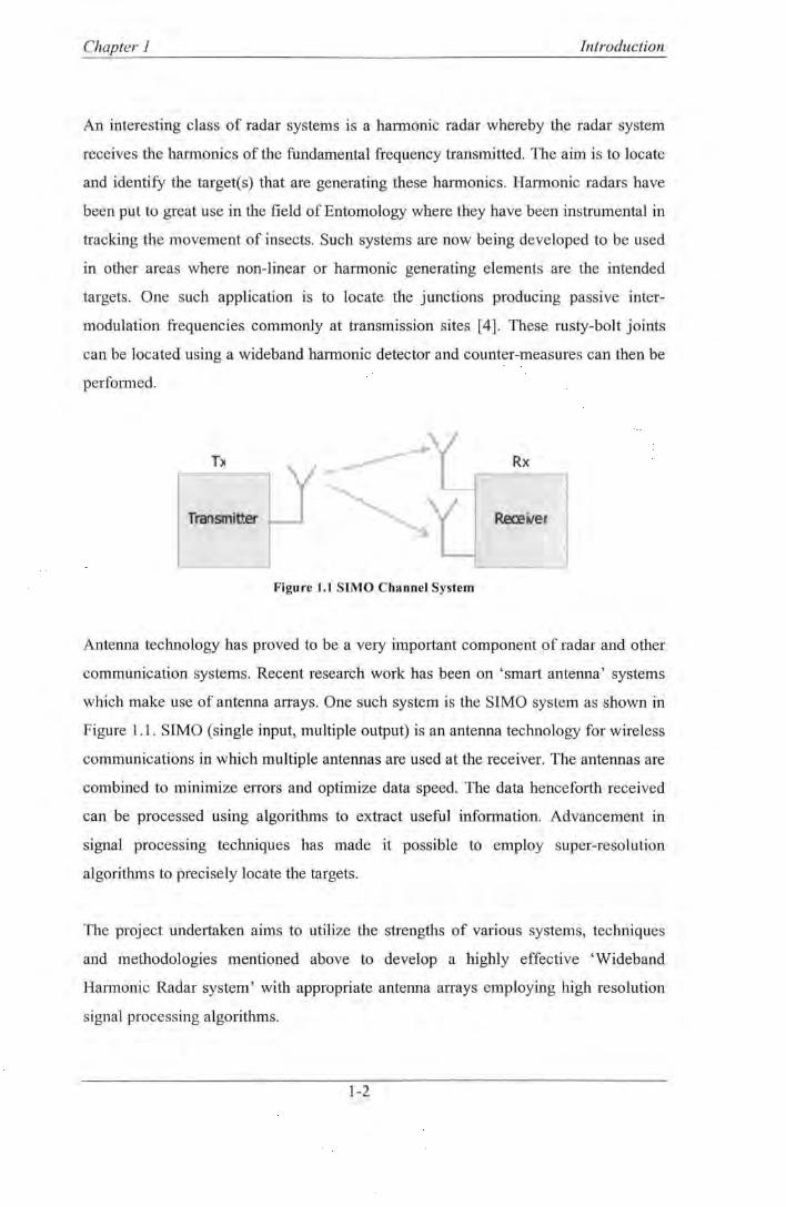
Rx
Transmitter Rece~er
Figure 1.1 SIMO Channel System
Antenna technology has proved to be a very important component of radar and other
communication systems. Recent research work has been on 'smart antenna' systems
which make use of antenna arrays. One such system is the SIMO system as shown in
Figure 1.1. SIMO (single input, multiple output) is an antenna technology for wireless
communications in which multiple antennas are used at the receiver. The antennas are
combined to minimize errors and optimize data speed. The data henceforth received
can be processed using algorithms to extract useful information. Advancement in
signal processing techniques has made it possible to employ super-resolution
algorithms to precisely locate the targets.
The project undertaken aims to utilize the strengths of various systems, techniques
and methodologies mentioned above to develop a highly effective 'Wideband
Harmonic Radar system' with appropriate antenna arrays employing high resolution
signal processing algorithms.
1-2

Chapter 1 Introduction
1.2 Review of Chapter Contents
Chapter 2 describes the FMCW Harmonic radar system in detail. It explains the
theory behind an FMCW waveform and gives an overview of the historical
development ofharmonic radar system.
Chapter 3 provides an overview of the Rusty-bolt Effect. It describes the reason
behind its occurrence and mentions the counter-measures available in literature.
Chapter 4 provides a system level overview of the harmonic radar. It also explains the
work done so far and gives an understanding of its various components.
Chapter 5 deals with signal processing algorithms. Two techniques are mentioned and
their underlying principle is explained.
Chapter 6 is the conclusion of the report. It describes the work accomplished so far
and the requirements needed in order to carry out developing the rest of the radar
system.
1-3

Chapter 1 Introduction
1.3 References
[1] H. D. Griffiths, Chris J. Baker, "Radar Imaging for Combating Terrorism",
Department of Electronic and Electrical Engineering, University College
London, London, UK
[2] W. W. Camp, J. T. Mayhan, R. M. O'Donnell, "Wideband Radar for Ballistic
Missile Defense and Range-Doppler Imaging of Satellites", Lincoln Laboratory
Journal volume 12, number 2, 2000
[3] M. I. Skolnik, Introduction to Radar Systems, 2nd ed: McGraw Hill, 1988
[4] "MPT 1331 : Code of Practice for Radio Site Engineering", June 2001, Flyde
Microsystems Ltd
1-4

Chapter 2 FMCW Harmonic Radars
Chapter 2
FMCW Harmo011ic Radars
2.1 Radar Theory & Principles
Radar measurement is based on the principles of properties of radiated
electromagnetic energy. Electromagnetic energy travels through air at approximately
the speed of light. This energy is transmitted to and reflected from the reflecting
object. A small portion of the reflected energy returns to the radar set. This returned
energy is called an 'echo'. Radar sets use the echo to determine primarily the
direction and distance of the reflecting object.
One of the most important relations used to define the working of a radar system is
the radar range equation. It relates the transmit power from the radar to the received
power in terms of range, antenna and target dimensions. The fundamental form of the
radar range equation is
(2.1)
where
Transmit Power • P r Receive Power • G Antenna Gain • R Target Range • a RCS - Radar Cross Section i.e. measure of size of target
as seen by the radar. Its units are that of area. • Ae Effective Aperture of receiving antenna
Two important parameters for radar performance is its resolution and sensitivity.
Resolution
The range resolution tells us how far apart two targets have to be to be distinguished
as two separate entities. If the time delay between the reflected signals from two
2-1

Chapter 2 FMCW Harmonic Radars
objects is greater than the pulse duration, then the two objects are seen separately.
[21] If the targets are closer than this duration, then the receiver will not be able to
distinguish between the two.
Sensitivity
The range sensitivity or accuracy indicates uncertainty in a measurement of the
absolute distance to an object. Intuitively, accuracy of a range measurement should
depend on the 'sharpness' of the pulse shape. However, the crucial factor determining
range accuracy is bandwidth. Consider a single wavelength being used to locate a
target. The target phase measured will be ambiguous every wavelength. A second
wavelength added to the transmission will aide in locating the target. It reduces
ambiguities and sharpens the position of the target. Adding more wavelengths means
increasing bandwidth. Therefore, adding more bandwidth leads to greater accuracy
and the system becomes more sensitive [21].
2.2 FMCW I Chirp Waveform
FMCW or Frequency Modulated Continuous Wave work on the principle of 'pulse
compression' or 'pulse coding'. It is a processing technique that maximises the
sensitivity and resolution of radar systems. Chirp signals derive their name from the
fact that if the signal was audible it would sound like the chirp or tweet of a bird. The
chirp of a bird increases monotonically over a frequency interval.
Chirp waveform was first classified by K.lauder et al. [ 1] as published in the Bell Labs
Technical Journal in 1960. However, the basic idea was presented earlier by Oliver in
1951 in a Bell Telephone Laboratory internal memorandum which was interestingly
titled "Not with a bang but a Chirp" [2].
Increase in radar sensitivity can be achieved by two methods.
1. By increasing the average transmitting power
2. By increasing the pulse length
2-2
Chapter 2 FMCW Harmonic Radars
Average transmitted power is the peak power multiplied by the transmitter duty cycle.
The peak power can be as high as several hundred kilowatts. However, a pulse radar
transmits short burst of pulses where the average transmit power might be 1% of the
peak transmit power. This makes such a system very inefficient. Increasing the pulse
length can increase the average transmitted power without decreasing efficiency but
this has an adverse effect of degrading the range resolution. The radio pulse is too
long and can not distinguish between two closely spaced targets.
This conflict in user requirements can be resolved in designing such a transmit
waveform that would maximise both sensitivity and resolution. As described above,
the range resolution does not necessarily depend upon the pulse length but on the
pulse bandwidth. The bandwidth can be altered by manipulating the amplitude and/or
phase within the pulse without changing its duration. Thus, the radar resolution can be
increased without having to change its duration. This manipulation of pulse is called
'pulse coding'. The types of pulses that involve changing the frequency of the
transmitted pulses are called 'chirp' pulses. This is an electronic method to boost the
apparent signal strength as perceived by the radar receiver. The outgoing radar pulses
are chirped, that is, the frequency of the carrier is varied within the pulse, much like
the sound of a cricket chirping.
The timing mark is the changing frequency. The transit time is proportional to the
difference in frequency between the echo and the transmitter signal. The greater the
transmitter frequency deviation in a given time interval, the more accurate the
measurement of the transit time and the greater will be the transmitted spectrum.
In FMCW radar, the transmitter frequency is changed as a function of time in a
known manner. This known manner can be linear or non-linear in nature.
A linear chirp waveform modulated signal can be defined by the following equations:
Xr (t) = A0 cos[~r (t )] (2.2)
where ~r(t)=2n(fct+ ~2
) (2.3)
2-3

Chapter 2 FMCW Harmonic Radars
and Ar ={Eo for 0 5, t ~ t '} 0 otherwzse
(2.4)
Here, the subscript T stands for transmitting, fo is the carrier frequency at t = 0, k is
the linear chirp rate and ~T(t) is the instantaneous transmitted phase. The time value
t' represents the length of the transmitted chirp signal. It is known that the
instantaneous transmitted frequency is specified by:
(2.5)
which implies Jr. (t)=fc+kt (2.6)
It is evident from the equation that the frequency increases linearly with time.
Therefore, the transmitted signal exhibits linear frequency modulation commonly
referred to as the saw-tooth signal shown in figure 2.1
+
Frequencr
Tllne
Fig 2.1 A Chirp Signal
This signal is generated repetitively a fixed quantity of times in a second. This
quantity is known as the Wave Repetition Frequency (WRF).
2-4

Chapter 2 FMCW Harmonic Radars
Freq ency
/ /
/
/
/ /
/; :/ .
/ /
/
/ /
/ ' / :v /
/ /
/
/ /
/
'4 TJE!I _..., , .,~T2=!I'o+ T
Transmitted chirp ------------- Received chirp Fig. 2.2 Resultant frequencies at the receiver (3)
Time
Figure 2.2 shows the resultant frequency at the receiver. Here it is possible to see
graphically all the parameters involved in the preceding sections. The solid line
represents the transmitted signal the dotted line shows the received signal. The
received signal is delayed by a time 1", with respect to the transmitted signal. If a
signal that is a replica of the transmitted signal is combined with the received signal,
then the resultant difference frequency will be a train pulse and the pulse width has a
frequency f0 . This can be used to extract useful information using a signal processing
technique. More of it is explained in Chapter 6.
For a linear chirp, the sweep rate is the slope of y-axis (frequency) to x-axis (time)
over a single chirp. Therefore, the sweep rate 'k' is
k=B T
and equation (2.2) becomes
xT (t) =AT cos[~T (t )] =AT eo{ 2tr/J ± n: t2)
where fc is the carrier frequency
AT is the amplitude of the transmitted signal and is constant
2-5
(2.7)
(2.8)

Chapter 2
B is the sweep bandwidth
T is the sweep period.
The instantaneous frequency ofthis signal is:
f (t) = _1 dt/Jr (t) = f" ± B t T 2;r dt J c T
For a linearly increasing chirp,
In this case,fc is the lower frequency of the bandwidth.
2.3 Harmonic Radar- Historical Development
FMCW Harmonic Radars
(2.9)
(2.10)
Harmonic Radar is a device that illuminates a region of space with RF waves and
receives the harmonics of the transmitted frequencies. The received data can then be
processed to find the exact locations of the points causing the generation of these
harmonics. It works on the principle of radar transmitting a chirp signal and receiving
harmonics of the transmitting frequency.
Radars were the earliest applications of chirp waveform. Barrick (4], Poole [5],
Klauder et al. [ 1] presented valuable works related to the theory of the FMCW signals
and its radar applications. With the development of electronic circuit techniques and
signal processing algorithms, this principle found new applications - one of them
being in area ofmobile radio channel characterisation as presented by Salous [6-7].
An early commercial FMCW Harmonic Radar system was METRRA - Metal Target
Re-Radiation developed for the US Army in the late 70's. [8] Its intended use was to
detect stationary military targets e.g. tanks, vehicles, and weapon caches etc. which
are hidden by foliage. The system transmitted a 400 MHz signal and received its third
harmonic (120 MHz) signal. It is reported to be successfully demonstrated at a range
of 1 kilometre. (8]
2-6

Chapter 2 FMCW Harmonic Radars
Another harmonic radar system was developed by the U.S. 'Strategic Environmental
Research and Development Program (SERDP)' which is the Department of Defense's
(DoD) environmental science and technology program. This system developed in the
late 90's third harmonics and used for Unexploded Ordinance (UXO) Detection. This
project built a prototype system that demonstrated capability to detect and locate
buried UXO remotely. [9]
Harmonic radars have also been an area of interest in academia. One such system was
developed at the Electromagnetic Laboratory at Michigan State University. Its
intended use was in etymology. This radar was a hi-static CW system. The transmit
frequency was 800- 900 MHz and the receiver could be tuned to from 1232 MHz to
1862 MHz. The system was intended to detect harmonic radar tags in high-clutter
environments. [ 1 0]
Recent developments in non-linear junction detectors (NLJD) have shown the
advancement and sophistication of new devices coming up. A number of patents have
been issued in the past few years.
Jones et al. [11] developed a non-linear junction detector for counter surveillance
measures. Its main feature is the use of a circularly polarized Tx/Rx antenna. Using
linearly polarized antenna, one has to scan the target area twice in a horizontal and
vertical position. This ensures that the surveillance device returning polarized
harmonic return do not go un-detected. Using a NLJD with circularly polarized
antenna allows successful detection regardless of which angle the scan is made.
Barsumian et al. [12] have developed an interesting NLJD that transmits a series of
pulses as the transmit signal. The transmit power of pulses is varied. The received
harmonics of all pulses are compared to each other as well as to a set of standard data.
The harmonic signals are analysed if they correspond to a known set of non-linear
device. The receive harmonics are also demodulated to the audible frequency range
where they are detected by an audio circuit. Some NLJDs have a feed back control
system in them such as developed by Holmes et al. [13]. The feed back control
maintains a pre-determined minimum threshold value of the received signals. So the
control system has two parts - one to determine the signal strength and other to vary
2-7

Chapter 2 FMCW Harmonic Radars
the power output level of the transmitter. Advantage of this invention is improved
system efficiency.
All of the systems mentioned above transmit at a single frequency and receive at
multiple harmonics. An innovative method is to transmit at multiple frequencies and
then try to receive different combination of its harmonics. One such invention is the
CWER (Concealed Weapon and Electronics Radar) system developed at John
Hopkins University by Jablonski et al. [14]. This system transmits two frequencies at
ft and f2 from separate antenna systems. This creates received signals of the order of
nft ± m6, where n and m are integers. A single frequency transmit has adequate
detection capability but it has very limited capability with respect to classifying
different types of targets. This Dual Frequency Scanning Harmonic Radar has the
ability to distinguish objects of different types and to distinguish them from nearby
clutter. Another recently patented invention was by Rafael-Armament Development
Authority Ltd. [ 15] This NLJD transmits more than two frequencies fl, f2, f3 ....
towards the area of interest. The receiving unit then tunes to receive at
intermodulation products nfl + mf2 + qf3 .... , wherein n, m, q are non-zero integers.
2.3.1 Non-Linear Junction Detector
The use of a Harmonic Detector, also called as a 'Non-Linear Junction Detector' is
dependent on the fact that electronic devices and metallic objects that come in contact
with one another create a non-linear junction. What a non-linear junction detector
does is detect these non-linear junctions. In doing so, active or inactive junctions can
be detected. One should keep in mind that these non-linear junctions can be anything
from electronic circuits like eavesdropping equipment (bugs, microphones etc) to
various corroded metal junctions. Various methods of analysis and algorithms can be
used to distinguish between the targets.
The two main functions of a sweep using Non Linear Junction Detectors are:
1. The Detection of non-linear junctions
2. The Discrimination between junctions so as to differentiate between
electronics and other forms of junctions
. 2-8

Chapter 2 FMCW Harmonic Radars
The RF sweep would be useless without the second step as there would be many false
alarms.
The junctions in electronic devices are different than those in other junctions. The
harmonic returns of electronics are well defined but that of non-electronics are not.
Electronic components will have a strong second harmonic signal and a weak third
harmonic signal. Other junctions will have a weak second harmonic signal and a
strong third harmonic signal [16]. The 3rd, 51h and other odd harmonic reflections are
reflected by any conductive or metallic surface. Fig. 2.3 shows graph of current and
voltage characteristics of a semi-conductor junction and a false junction.
I
J V
I J
) wl V
( Semiconductor Junction
Characteristics I False Junction I . -Characteristics
Fig. 2.3 IV- graphs for non-linear junctions [17]
The non-linear characteristics of semiconductor junctions differ from false junctions:
the 2nd and 3rd harmonic signals will have different intensities. When a NLJD
radiates a semiconductor junction, it results in a 2nd harmonic stronger than the 3rd
harmonic. A false junction returns a 3rd harmonic that is stronger than the 2nd
harmonic.
2-9
Chapter 2 FMCW Harmonic Radars
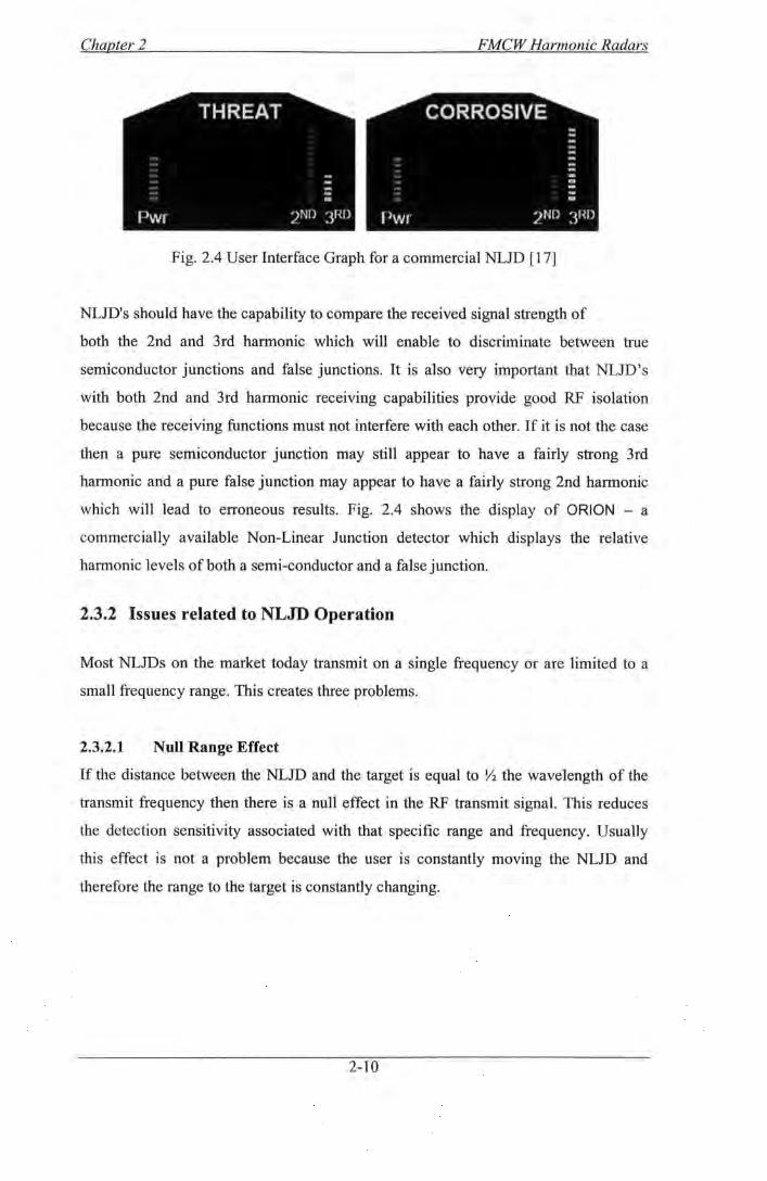
Fig. 2.4 User Interface Graph for a commercial NLJD [I 7]
NLJD's should have the capability to compare the received signal strength of
both the 2nd and 3rd harmonic which wiii enable to discriminate between true
semiconductor junctions and false junctions. It is also very important that NLJD's
with both 2nd and 3rd harmonic receiving capabilities provide good RF isolation
because the receiving functions must not interfere with each other. If it is not the case
then a pure semiconductor junction may stiii appear to have a fairly strong 3rd
harmonic and a pure false junction may appear to have a fairly strong 2nd harmonic
which wiii lead to erroneous results. Fig. 2.4 shows the display of ORlON - a
commerciaily available Non-Linear Junction detector which displays the relative
harmonic levels of both a semi-conductor and a false junction.
2.3.2 Issues related to NLJD Operation
Most NLJDs on the market today transmit on a single frequency or are limited to a
smaii frequency range. This creates three problems.
2.3.2.1 Null Range Effect
If the distance between the NLJD and the target is equal to ~ the wavelength of the
transmit frequency then there is a nuii effect in the RF transmit signal. This reduces
the detection sensitivity associated with that specific range and frequency. U suaily
this effect is not a problem because the user is constantly moving the NLJD and
therefore the range to the target is constantly changing.
2-10

Chapter 2 FMCW Harmonic Radars
2.3.2.2 Target Dependence on Frequency
It is often observed that NLJD's perform differently for different targets. This is
because detection range is dependent on frequency. Consider a cellular phone as a
potential target. If an NLJD operates at a frequency that is within the operational band
of the cellular phone, then the detection range of the phone will be large, however, if
the NLJD operates at a frequency range that is outside of the operational band of the
cellular phone, then the built-in filters within the phone will attenuate the NLJD signal
and the detection range will be greatly reduced.
2.3.2.3 Frequency Interference
If the NLJD is operating on a frequency that may also be occupied by another
transmitter, the NLJD may have very erratic and unreliable readings. As more
wireless devices are being assigned to more frequencies, the performance of these
limited NLJD units can suffer. NLJD should be frequency agile and automatically
search for quiet channels on which to operate to avoid frequency interference from
other devices.
One commercial NLJD ORlON™ [20] addresses the above mentioned problems
using two methods: Quiet Channel Search and Frequency Hopping. In normal search
mode, the ORlON™ automatically searches for the quietest channels on which to
operate in the ambient environment. The new frequency hopping search method
employs an algorithm that constantly changes the transmit frequency over the full
legal range to increase the target hit rate.
A list of popular NLJD's used in the commercial market is given in a tabular format
below listing their main parameters:-
Company Product Frequency Power Antenna (MHz) Polarization
AudioTel, U.K. SuperBroom Tx- 888.5 EIRP- Tx-Linear R:xl-1777 +40dBm R:x - Circular Rx2- 2665.5
Research ORlON Tx- 850-Electronics, U.K. 1005
R:xl- 1700- 1.4W Tx - Circular
2-11

Chapter 2 FMCW Harmonic Radars
2010 Rx - Circular Rx2 -2550-3015
Surveillance Eclipse Tx- 890-895 2W Consulting Group, Rxl-1780- Tx - Circular Switzerland 1790 Rx - Circular
Rx2 -2670-5370
Information Security Boomerang Tx- 915 100mW, Tx-Linear Associates, U.S.A. Rxl-1830 500mW Rx- Linear
Rx2 -2745
2.3.3 Further Applications
FMCW Harmonic Radars can also be used in many other different applications such
as:-
1. Radar Entomology i.e. tracking of insects' movements e.g. Butterflies, Bees,
and Snails etc.
2. Unexploded Ordinance Detection (Third Harmonic Detection)
3. Electronic counter surveillance i.e. Detection of 'bugs' implanted by enemy
agents. Professional investigators or "spies" sometimes use many electronic
devices that do not utilize radio frequency transmissions. The NLJD will
detect and locate any electronic device regardless of whether or not the device
is powered.
4. Measurement of thickness of ionizing layer in space and upper atmosphere
2.4 Harmonic Radar Range Equation
The basic radar range equations can be used to develop the range equation for
harmonic radar. This can be subsequently used to calculate the power link budget.
Colpitts & Boiteau [ 18] developed the range equation for harmonic radar to be used
for insect tracking. The target was a harmonic 'tag' (a dipole and an inductive loop)
which would be planted on insects to track them.
2-12

Chapter 2 FMCW Harmonic Radars
The Friis Transmission equation is given as
p = p G,G,A-z r ' (4nR)2
(2.11)
The Harmonic Radar Range Equation can be developed in a similar manner as the
conventional radar except that a harmonic cross-section should be replaced for radar
cross-section. The harmonic cross-sectional area of the tag is described as follows:
(2.12)
where ~,hGdh -Effective isotropic radiated power (EIRP) from the tag at the second
harmonic. Its units are Watts.
Wdf- Fundamental frequency power density incident upon the tag in units of
W/m2
The power density incident upon the tag is given by
W - JJ.t[Gsf df- 4nRz
where P.tf -Radar transmit power
G.1 - Gain of the transmit antenna
R - Distance between radar and tag
(2.13)
The EIRP of the illuminated tag is the power transmitted from the tag at the second
harmonic multiplied by the antenna gain of the tag at the second harmonic.
(2.14)
2-13

Chapter 2 FMCW Harmonic Radars
The received second harmonic power from the tag back to the radar can be calculated
as
(2.15)
where Gsh - Receive radar antenna gain at the second harmonic frequency
'Ah - Harmonic wavelength
The ratio of the received second harmonic power to the radar transmit power at the
fundamental frequency is given as
(2.16)
Jenn [ 19] developed a generalised harmonic radar range equation for the third
harmonic given as
p = (~G,tG),-/crh r ( 4Jr t+2 R2a+2
(2.17)
where a ~2.5 is a non linear parameter determined experimentally. It varies slightly
from target to target.
2-14
Chapter 2 FMCW Harmonic Radars
2.5 References
[1] Klauder J. R., Price A. C., Darlington S., and Albersheim W. J., "The Theory and
Design of Chirp Radars ", The Bell System Technical Journal, July 1960, Vol. 39,
No. 4, pp 745-815
[2] B.M. Oliver, Bell Telephone Laboratories Technical Memorandum, MM51-150-
10, Case 33089, March 8, 1951
[3] V. M. Hinostroza, "Indoor Wideband Mobile Radio Channel Characterisation
System", UMIST PhD Thesis, 2002
[4] Barrick D. E. " FMCW radar signals and digital processing". NOAA technical
report, ERL 283-wpl26
[5] Poole A. W. V., "Advanced sounding. The FMCW alternative", Radio Science,
December 1985, Vol. 20, No. 6, pp 1609-1619.
[6] Salous S., and Nickandrou N. "Architecture for Advanced FMCW Sounding",
International Journal in Electronics, 1998, Vol. 84, No. 5, pp. 429-436.
[7] Salous S., Nikandrou N., and Bajj N.F., "Digital techniques for mobile radio chirp
sounders ", lEE proceedings Communications, June 1998, Vol. 145, No. 3, pp.
191-196.
[8] The Field Artillery Journal, March-April 1977 pp. 50-51, http://sill
www.army.mil/famag/1977/ [accessed lih Feb. 2008]
2-15

Chapter 2 FMCW Harmonic Radars
[9] J. Kositsky, (2001), Unexploded Ordnance (UXO) Detection by Enhanced
Harmonic Radar, http://www.p2pays.org/ref/20/1940 1.pdf [ accessed 171h Feb.
2008]
[10] Gregory L. Charvat, Edward J. Rothwell, Leo C. Kempel, "Harmonic Radar
Tag measurement", Michigan State University, (2003)
[ 11] THOMAS H. JONES. 2000. Non-Linear Junction Detector. US006057765A.
[12] BRUCE R. BARSUMIAN. 2000. Pulse Transmitting Non-Linear Junction
Detector. US006163259 A
[13] STEVEN JOHN HOMES. 2005. Non-linear junction detector.
US006897777B2
[14] DANIEL G. JABLONSKI. 2004. System and method of radar detection of
non-linear interfaces. US006765527B2
[15] ITZHAK SCHNITZER, 2007. Radar system and method for locating and
identifYing objects by their non-linear echo signals
[16] Ralph D. Thomas, (1999), The Detection of Active and Non-Active
Eavesdropping Devices Buried In Walls and Furniture,
http://www.pimall.com/nais/n.junction.html [accessed 17th Feb. 2008]
[17] Thomas H. Jones, (1999), An Overview of Non-Linear Junction Detection
Technology for Countersurveillance, www.reiusa.net/system/products/NJE-
4000/NLJDTech.pdf [accessed 17th Feb. 2008]
[ 18] Bruce G. Colpitts and Gilles Boiteau, "Harmonic Radar Transceiver Design:
miniature Tags for Insect Tracking", IEEE Transactions on Antennas and
Propagation, Nov. 2004, Vol. 52, No. 11, pp 2825 - 2831
2-16

Chapter 2 FMCW Harmonic Radars
[ 19] Professor David Jenn, "Microwave Devices & Radar", Lecture Notes, Volume
IV, Naval Postgraduate School, www.dcjenn.com/EC4610NoliV(v4.7.2).pdf
[accessed 17th Feb. 2008]
[20] "ORlON™, Non-Linear Junction Evaluator: Operating Manual" Version 2.1,
(2005), Research Electronics International
[21] S. Kingsley, S. Quegan, "Understanding Radar Systems", McGraw-Hill, 1992
2-17

Chapter 3 Rusty Bolt Effect
Chapter 3
Rusty Bolt Effect
3.1 Introduction
Radio transmission sites are vulnerable to corrosion and rusting with the passage of
time. These deteriorations can appear randomly at different locations which can be
scattered over the entire site. They can result in erroneous frequency transmissions.
The main reason of the appearance of these impairments is a phenomenon called as
the 'Rusty Bolt Effect'.
Radio sites consist naturally of metallic structures. Metals are always covered by an
oxide film due to the metal reacting chemically with the oxygen in air. The rate of this
oxide formation depends largely on the environment. Any oxide film between
metallic contacts will cause non-linearity.
RF currents passing through these junctions would generate harmonics. When RF
signals at two frequencies f1 and f2 pass through a non-linearity they create signals at
their sum and difference frequencies (f1 - f2) and (f1 + f2). These are known as 'inter
modulation products'. This generation of inter-modulation products when radio waves
interact with rusty parts is called as the 'Rusty Bolt Effect'. It is also known as
passive inter-modulation abbreviated as PIM.
~~~a...~.~. lntermodulation in a metal structure e 'rusty bolt effect')
Transmitting antennas radiilll! at/1 and/2
Some of1his RF energy couples with 1h e metal structure of1h e tow er
Figure 3.1: Rusty Bolt Effect [11
3-1

Chapter 3 Rusty Bolt Effect
Radio spectrum is carefully controlled for optimal usage of the available frequencies
so that different services operate in well-defined frequency channels. Inter-modulation
creates frequencies that can be difficult to control and would cause interference in
channels reserved for other uses. Studies have shown that PIM distortion has caused
problems in naval and land communication systems. [2]
PIM distortion was first identified during the early 1940's [3]. Studies were done on
systems with antennas containing rusty-bolt parts. The detailed understanding of the
phenomenon was not present at that time but the idea of rust prevention to reduce PIM
was known.
3.2 Passive lntermodulation
3.2.1 Mathematical Representation
PIM components can be represented using mathematical equations. Consider current
passing through a rusty point. The relationship between current and voltage will not
be completely linear. It will contain harmonic frequencies and their linear
combinations.
The voltage transfer characteristic of a non-linear system can be described as
(3.1)
Consider an input signal consisting of two sinusoidal frequencies CD 1 and CD2
represented as
(3.2)
where CD = 2nf
The contribution from the second term is given as
Using the trigonometric relation
3-2

Chapter 3 Rusty Bolt Effect
cos2 () = (1 +cos 20) I 2
we can reduce Eq. (3.3) to
a 2 v; 2 (t)
az[A12 I 2+ Az 2 12 + 112A1
2 cos2aV + 112A/ cos2wzt + 2A1Az coswlcosw2t](3.4)
Using the trigonometric relation,
Eq. (3 .4) can be converted to
a 2 V;2 (t) = az[11 2(~2 + Az2 )+ 112(~2 cos2wl + Az2 cos2w2t)+
~Az{cos(w1 +w2 )tcos(w1-w2 )t}] (3.5)
We can see the output contains de component, second harmonics of the input
frequencies and intermodulation products at the sum and difference frequencies.
Consequently, from Equation (3.5) third, fourth and higher harmonics will be present
depending on the non-linear characteristic.
3.2.2 MPT 1331: Code of Practice for Radio Site Engineering
In order to assist radio system designers to minimise such interferences, Ofcom has
set some standards for radio site engineering. This set of standards is given in the
document 'MPT 1331: Code of Practice for Radio Site Engineering'.
Sections of the code emphasize on different aspects of radio engineering to make the
sites operate effectively. Section (3.1) deals with the sources of generation of
unwanted inter-modulation products, Section (3.4) describes the Corrosion &
Climatic effects on the radio sites and Section (5) describes some recommendations to
control inter-modulation and unwanted products. [6]
Any transmission site which is not following these codes would likely cause
interference to other users. It is important that radio engineers should check the sites
for their compliance with these codes.
3-3

Chapter 3 Rusty Bolt Effect
If a particular radio site is causing interference due to the rusty-bolt effect, the
corroded points must be located to minimize their effect.
3.3 Localization Techniques
3.3.1 Audio Detector - Laboratory Model An audio detection technique can be used to demonstrate the presence of PIM
products. One such system was developed by Bailey [ 4] as a 'rusty-bolt simulator'.
The system consists of two oscillators of known frequencies representing two signals.
These are then mixed using a diode. The resultant frequency is then mixed with
another frequency provided by a variable frequency oscillator (VFO). The VFO can
be tuned so that the output of the mixer remains between 2 and 8 kHz. This can then
be detected using a speaker.
In the lab demonstrating kit mentioned above, two oscillator frequencies were 4 and 6
MHz, the intermodulation frequency was 10 MHz and the VFO was 9.992-9.998
MHz.
3.3.2 Microwave Holographic lmaging
Microwave Holographic Imaging is a well established and an efficient technique to
locate PIM sources.
Aspden et al. [5] have used this technique to image intermodulation product sources
on reflector antennas. Two signal sources at 7.2GHz and 7.7GHz illuminate a
parabolic reflector. It is then scanned for the third order IMP at 8.2GHz. This was
done by trying to lock the received signal with a reference signal. The reference IMP
signal is generated by a non-linear diode.
3-4

Chapter 3 Rusty Bolt Effect
3.4 References
[1] Preventing Intermodulation, Radio communications Agency: EMC Awareness, www .ofcom. or g. uk/static/archive/raltopics/research/RA webPages/Radiocomms/pages /mittechlinstalllintermod.htrn [ accessed 2nd May, 2007]
[2] P. L. Lui, "Passive intermodulation interference in communication systems," Electron. Commun. Eng. J, vol. 2, pp. 109-118, June 1990.
[3] Reuven Shavit, (2003) "Intermodulation Distortion in Metal Space Frame Radomes", www.l-3com.com/essco/resources/IMP-MSF.pdf [accessed 20th Feb. 2008]
[4] Brandt Bailey, John Schneider (1999), Rusty Bolt Simulator, www.ece.ndsu.nodak.edu/-glower/design/projects/sp99/90 _rust. pdf, [ accessed 20th Feb. 2008]
[5] Aspden, P.L. Anderson, A.P. Bennett, J.C. , "Microwave holographic imaging of intermodulation product sourcesapplied to reflector antennas", Antennas and Propagation, 1989. !CAP 89., Sixth International Conference on , 463-467 vol., Apr 1989
[6] "MPT 1331 : Code of Practice for Radio Site Engineering", June 2001, Flyde Microsystems Ltd.
3-5

Chapter 4 System Description
Chapter 4 System Description
4.1 Introduction
The Harmonic Radar envisioned for the project is a mono-static wideband FMCW
radar system with a suitable receive antenna array. The received waves would then be
processed using super-resolution algorithms to accurately locate the target. A
conceptual diagram of such a system is shown in Fig 4.1.
Tx
Synchronization & Control
Antenna _j Tx
Rx
DSP
Answer
I lra,.,.iTlif WiV••>
RxAntenna Array
""-• N - C hannels
Target
Figure 4.1 System Conceptual Diagram
. I § :. •
The 'Tx ' block represents the transmitter which transmits a frequency at lGHz. The
'Rx' block represents the receiver. It can receive the harmonic frequencies at 2GHz,
3GHz and so on through an antenna array. The DSP represents the digital signal
processing block which processes the data. There is also a need for a separate sub
system that would control and synchronize between the three distinct blocks.
4-1
Chapter 4 System Description
4.1 System Design
::0
I· Transmitter
I -.--"'------~-----, I
Signal Conditioning + Data Acquisition 1
L _____ _J
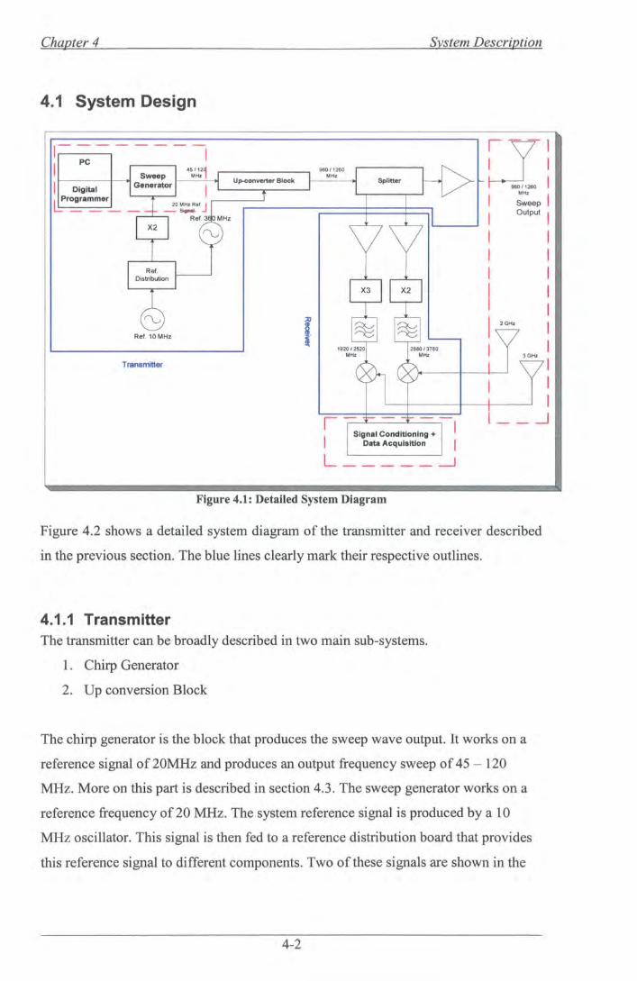
Figure 4.1: Detailed System Diagram
:.Y I I I I I I
I I 20Hz
MHz
Sweep Output
JGHz
I_- _j
Figure 4.2 shows a detailed system diagram of the transmitter and receiver described
in the previous section. The blue lines clearly mark their respective outlines.
4.1.1 Transmitter The transmitter can be broadly described in two main sub-systems.
1. Chirp Generator
2. Up conversion Block
The chirp generator is the block that produces the sweep wave output. It works on a
reference signal of 20MHz and produces an output frequency sweep of 45 - 120
MHz. More on this part is described in section 4.3. The sweep generator works on a
reference frequency of 20 MHz. The system reference signal is produced by a 10
MHz oscillator. This signal is then fed to a reference distribution board that provides
this reference signal to different components. Two of these signals are shown in the
4-2
Chapter 4 System Description
diagram. The first is multiplied with a 'times two' multiplier to provide the reference
signal for the sweep generator. The second provides the reference signal for the PLL
synthesizer that produces a signal of 360 MHz which is then used in the up
conversion block.
The up conversion block is a complex sub-system required to up-convert the sweep
frequencies coming from the chirp generator to the required transmit sweep centring
at I GHz. The required output sweep from the up-converter block is 960 - 1260 MHz.
This would realistically require stages of up-conversion from the lower frequency to
intermediate levels and then to the RF level. This would translate to the use of
components of mixers, LO's (local oscillators), multipliers, amplifiers and band-pass
filters to remove the spurious frequencies. The RF frequency is then split into three
parts. One is transmitted after amplifying through a high power amplifier. The other
two are then passed onto to the receiver to be used in the channels for super
heterodyne down-conversion.
4.2.2 Harmonic Receiver
The harmonic receiver primarily consists of two main channels. It will receive the
harmonics of the transmit frequency at 2GHz and 3GHz through a receive antenna
array. The two down-conversion channels coming from the transmitter are amplified
and then up-converted using 'times two' and 'times three' multipliers. The output is
then filtered to give a clean signal at 1920 - 2520 MHz and 2880 - 3780 MHz
respectively. These two channels are needed to perform super heterodyne down
conversion on the receiving harmonic waves. This down-conversion is performed
using two mixers.
The output of the mixers would be converted to digital data. It can then be digitally
processed using advanced algorithms to obtain useful information. A detailed
description on the signal processing can be found in Chapter 5.
4-3

Chapter 4 System Description
4.2.3 Antenna Array
The radar antenna array is an important part of the system. The system requires one
transmit antenna and two or more receive antennas. The important factors deciding
the selection of antenna are: -
Bandwidth, and
Directivity
Bandwidth of any antenna can be defined as the maximum frequency range over
which the antenna meets a defined specification. [ 1] Therefore, the system
requirements are a directional antenna covering a wide bandwidth for transmitter
(960-1260 MHz) and receiver array (1920-2520 MHz and 2880-3780MHz). Different
antennas were studied in literature that would satisfy these two main conditions. A
good option would be horn antennas which have been mentioned in literature. [2]
Figure 4.3: Log-Periodic Antennas (900-2600 MHz) [4)
The candidate wideband directional antennas are:-
1. Horn
2. Log-Periodic
3. Discone
4. Modified Patch Antennas
5. Conical Spiral with cavity
6. Log Spiral with cavity
4-4
Chapter 4 Svstem Description
Log-periodic antennas were ordered as shown m Figure 4.3 depending on the
availability and price.
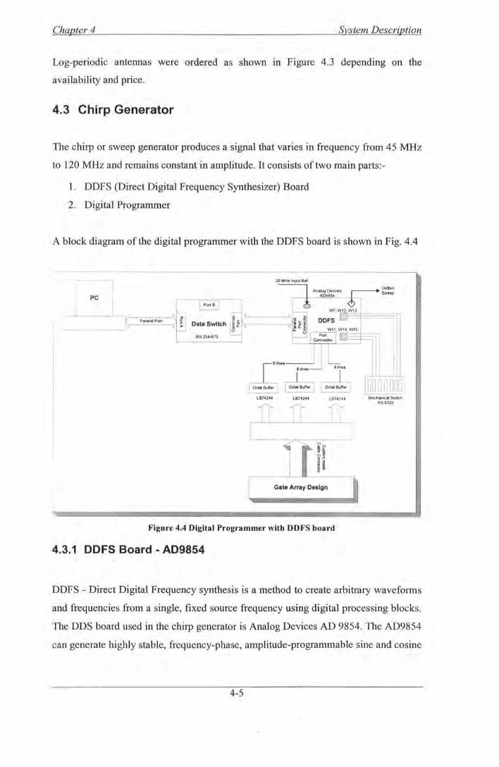
4.3 Chirp Generator
The chirp or sweep generator produces a signal that varies in frequency from 45 MHz
to 120 MHz and remains constant in amplitude. It consists of two main parts: -
1. DDFS (Direct Digital Frequency Synthesizer) Board
2. Digital Programmer
A block diagram of the digital programmer with the DDFS board is shown in Fig. 4.4
20 MHz Input Ref
PC ~ An·~~.~~~.. ~ OuWut ~~~ sw .. p
W7, W 12 W 13
Data Switch DDFS
RS 254~73
41ines
I Oc1~Bt I LSH244
Gate Array Design
Figure 4.4 Digital Programmer with DDFS board
4.3.1 DDFS Board - AD9854
DDFS - Direct Digital Frequency synthesis is a method to create arbitrary waveforms
and frequencies from a single, fixed source frequency using digital processing blocks.
The DDS board used in the chirp generator is Analog Devices AD 9854. The AD9854
can generate highly stable, frequency-phase, amplitude-programmable sine and cosine
4-5

Chapter4 System Description
outputs that can be used in many applications. Some of the available features of this
board are:-
Programmable Ref. CLK Multiplier
Control Register Data
Control Register Address
Frequency Resolution
Frequency Step Resolution
4 to 20
8 bits
6 bits
48 bits
48 bits
The AD9854 has five programmable operational modes. Three bits in the control
register called as Mode 0, Mode 1 and Mode 2 must be programmed to select the type
of operation. The different mode bits selections and their result are shown in table
below:
Mode2 Model ModeO Result 0 0 0 Single Tone 0 0 1 FSK 0 1 0 RampedFSK 0 1 1 Chirp 1 0 0 BPSK
The AD9854 supports linear as well as nonlinear FM sweep patterns. The different
parameters needed to program the chirp mode are:-
• Start Frequency Tuning Word (FTW 1)
• Time steps (Ramp rate)
• Frequency steps (Delta frequency)
• 110 UD Clock
• Clear Accumulator 1 Bit (CLR ACC1)
Other controlling parameters present on the DDS board are:-
• Clear Accumulator 2 Bit (CLR ACC2)
• FSK bit (Frequency Shift Keying)
• BPSK bit (Binary Phase Shift Keying)
4-6

Chapter 4 System Description
~ V V V V V 5
/ ~ F1 1--
0
MODE 000 (DEFAULT) 0111CHIRPJ
FTW 1 0 f1
OfW DELTA FREQUENCY WORD
RAMP RATE RAMP RATE
I I uo uo CLK ___ ____Jn._ _ __.n~.... _ __.n~.... _ __.n~.... _ __.n~.... _ ____Jn_ CLRACC1 __ _..
Figure 4.5 Chirp Mode Operation [3]
Fig. 4.5 illustrates the functioning of a simple chirp mode. It is important to note that
FTWl is only a starting point for FM chirp. There is no built-in restraint requiring a
return to FTWl. However, instant return to FTWl can be achieved by interrupting the
current chirp, reset the frequency back to FTWl, and continue the chirp at the
previously programmed rate and direction.
A program was developed in Visual Basic that would calculate all the required Chirp
mode parameters. The user interface of this program is shown in Figure 4.6
... I me.tr r MC.W P.uNf'lf!ters C<!lculdto r ~lf~~
BW f"'' Tsys 1,..., Calculate BW I
WRF !teotl Tau ltot4 Calculate WRF I I or Tau
Calculate Tau from BW
r Tfrom N r N lromT
- 1/0 UO Puloo [i;;:;o--- N r--- Calculate T or N J
r Delta t from N' r N' from Delta t
Delta t 1Te>t7 N ' Jrm:a- Caculate deltaT
or N' -vo UDPulsa IT...S rj';tji)"-·N·"~~.-., .... __
idth delta f
~1/0UD J -~~-H
Figure 4.6: User Interface of Chirp Mode Parameter Calculator
4-7

Chapter 4 System Description
This program uses a set of standard equations available in literature to calculate the
required parameters. The equations are described below:
-t-
.-.---T---....
--- Tau----.
Figure 4.7: Relationship of 1/0UDCLK and Output Chirp
All the equations that follow refer to figure 4.7 above.
1/0 UDCLK
Output Chirp
The time period T of the chirp is related to the system clock by the relation
T = (N + 1)(-z:ys X 2) (4.1)
where T.ys is the DDFS system clock.
The time step value in Fig. 4.5 is !1t. It IS related to the system clock with a
counter N'. Their relation is given as
The width of the VO UDCLK pulse is related to the system clock by
f = 8J:ys
By definition ofBW,
BW = n11f
The relation of time period and step-time for the chirp is given as
4-8
(4.2)
(4.3)
(4.4)
Chapter 4
T n=-
!!it
System Description
(4.5)
Replacing Eq. (4.5) into Eq. (4.4) gives us
BW = T !1f 11t
But since
r=T Therefore we have,
(4.6)
(4.7)
(4.8)
These equations have been used in the VB program to calculate the required
parameters to generate a chirp depending on the parameters entered by the user.
Ref 0 dBm Peak Log 10 dB/
I
M1 S2 S3 FC ,
RR I
Start Res BW 1 MHz
Atten 10 dB
1R
t:. Mkr1 - 100.5 MHz 2.134 dB
-----· ----·--- ._..,.,;._ __ - ~l Stop 200 MHz
VBW 1 MHz Sweep 4 ms ( 401 pts)
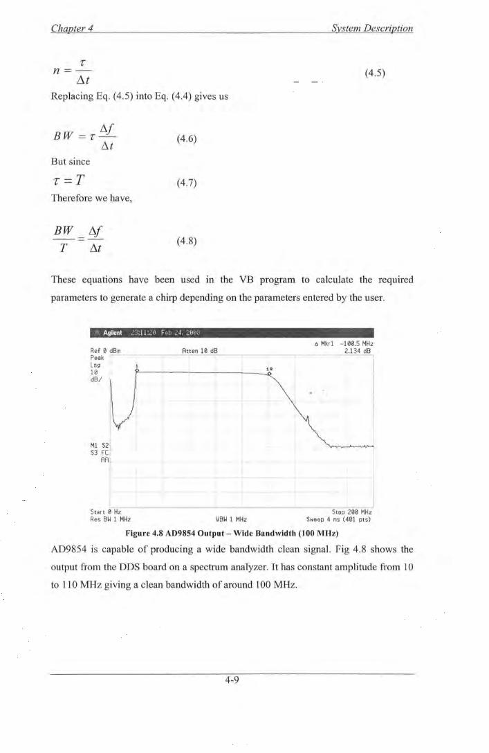
Figure 4.8 AD9854 Output- Wide Bandwidth (1 00 MHz)
AD9854 is capable of producing a wide bandwidth clean signal. Fig 4.8 shows the
output from the DDS board on a spectrum analyzer. It has constant amplitude from 10
to 110 MHz giving a clean bandwidth of around 100 MHz.
4-9

Chapter 4 System Description
Ref 0 dBm Peak I Log
Atten 10 dB o Mkr1 -75.0 MHz
1.693 dB
10 dB/
Ml S2 j $3 FC ,
AA
Start 0 Hz Res BW 1 MHz
1 R
VB~ 1 MHz Stop 200 MHz
Sweep 4 ms (401 pts)
Figure 4.9 AD9854 Output- 45/120 MHz
Fig 4.9 shows the output from AD9854 when operating in the sweep generator. It
produces a sweep from 45 MHz to 120 MHz with almost constant amplitude. The
bandwidth thus achieved is 75 MHz.
5.3.1.1 Waveform Designing
Wavefom1 designing is an important area of research in radar signals. The type and
quality of information received by radar depend in part on the waveform it transmits.
Efficient waveforms minimize the ambiguities present in FMCW radar system. One
such practical solution has been presented by Salous [5] where a multiple WRF signal
was introduced as a solution to range/Doppler ambiguity. This goes back to the
pioneering work by Poole [6] where he introduced a multi-cell waveform.
More advanced waveforms than the basic linear chirp signal were studied to be
implemented with the DDS AD9854. The result has been summarized in the table
below: -
Waveforms AD9854 Signals Used
1. Linear Chirp I/0 UDCLK, CL RA CC 1
2. Triangular Modulation I/0 UDCLK, FSK/BPSK bit (Ramped
4-10

Chapter 4 System Description
FSKMode)
3. Linear FM Ranging 110 UDCLK, CLRACC2 (A variant of
Chirp Mode)
4. Segmented Linear FM 110 UDCLK, FSK/BPSK bit, CLRACC2
5. Multi-cell Chirp Not possible without adding external
hardware circuit
6. Staggered WRF This can be programmed m the Chirp
mode using the signals 110 UDCLK,
CLRACCl. The critical part would be
programming new ~ f and/or ~t values
after every single chirp.
7. Multiple WRF This is the same as above except that new
~f and/or ~t values must be
programmed after a number of individual
chirps as defined by the WRF.
5.3.1.2 Phase Coherency
An important consideration is the phase component of the transmitting signal. The
Chirp mode by default has an internal problem for our applications. The CLR ACC 1
signal only clears the Frequency Accumulator. It does not affect the Phase
Accumulator value. The frequency changes of the DDS become phase continuous, but
not phase coherent. When a new frequency is programmed into the DDS, the next
phase will simply be incremental with respect to the last phase value in the phase
accumulator, and therefore the output sine wave will be phase continuous.
This phase continuity will cause a problem in the harmonic detector. There will
always be a phase component present in the transmitting signal and therefore in the
receiving signal. This phase component will appear as a Doppler or a movement I
velocity in the end data. Thus, if the DDS is used as such, it will show a Doppler
component of an object without any actual movement present.
4-11
Chapter 4 System Description
Some modifications either in the source code of the program or with some additional
external hardware circuitry is needed to clear the phase accumulator along with the
frequency accumulator.
The CLR ACC2 control bit (Register Address lF hex) is available to clear both the
frequency accumulator (ACCl) and the phase accumulator (ACC2). When this bit is
set high, the output of the phase accumulator results in 0 Hz output from the DDS. As
long as this bit is set high, the frequency and phase accumulators are cleared, resulting
in 0 Hz output. To return to the previous DDS operation, CLR ACC2 must be set to
logic low. This bit can be used to clear the phase of the signal along with the
amplitude.
However, we cannot afford to keep the CLR ACC2 bit high for a long duration.
Otherwise it will result in an ON/OFF Keying pattern.
Solutions were designed so as to clear the ACC2 bit before the start of the next chirp.
This would require a number of steps as follows:
• The DDS board should be programmed from a circuitry controlled by the
user. For this, a cable was built to connect the junction pins on the board with
a test board. These pins can then be used to control the DDS by sending in
appropriate control commands at the correct addresses.
• The CLR ACC2 bit requires a signal that would clear the output in between
the end of the first chirp and start of the next chirp. This 'high' time should be
as low as possible so as not to severely distort the shape of the end waveform.
4-12

Chapter 4 System Description
O~OisplayUnit Oadllose:o,_/ DOS
Sp.c:trvmAnlllyaar AD 9854
Data Disptay Unit Oscilloscope I DOS
Spectrum Analyser AD9854
I L ~ .<::;["'-
""' 7
Mono .-table Multi-Manu• Controllar lnlerf~
VIbrator ~7
~ 1 I
I
J.K Flip Flop Manual Controller Interface
OR Gata
I I.M.,Addi!IDn
Figure 4.10: Block d iagram of external hardware Figure 4.11: Block diagram of external to generate the CLR ACC2 signal hardware to generate the CLR ACC2 signal
The circuit performs the following functions:
1. All the signals provided in the junction J1 0 on the DDS board are connected to
a test board via a cable.
2. The Manual Controller allows the user to send control words at appropriate
addresses.
3. The VO Update Clock is then sent to a mono stable multi-vibrator (74121)
which generates a longer version of the UD CLK pulse width depending on
the resistor and capacitor values selected.
4. This longer pulse was then sent as CLR ACC2 signal back to the DDS board
through the manual controller.
This solution did not work. The reason for this was that the output of the multi
vibrator occurs after a certain amount of delay from the input UD CLK signal. For the
phase accumulator to be cleared, the two signals VO UD CLK and CLR ACC2 must
start at exactly the same time.
A slight modification in the circuit can achieve this quite easily. An additional OR
gate was added to the circuit as shown in Fig. 4.10
4-13

Chapter4 System Description
1. One input to the OR gate is the VO VD CLK signal.
2. The other input is the output of the multi vibrator signal.
3. The output signal from the OR gate would be a wider pulse that starts at
exactly the same time as the VO VD CLK. This signal was then sent as the
CLR ACC2 signal to the DDS board through the manual controller.
This solution also failed to clear the phase accumulator.
In order to diagnose the problem, an attempt was made to provide such signals which
are the exact replica as that in Fig 4.11. The CLR ACC2 signal has a period that is the
exact twice of the VO UD CLK period. Such a signal can be generated using a J-K
Flip Flop. The block diagram of such a circuit is shown in Fig. 4.11.
1. The VO UD CLK signal is sent from the manual controller to a J-K Flip Flop.
2. The J-K Flip Flop is set in a toggle mode.
3. It then generates a signal that has a period exact twice that of the I/0 VD
CLK.
4. This signal is then sent as the CLR ACC2 signal to the DDS board via the
manual controller.
This design does clear the phase at the start of every chirp. However, it also clears the
amplitude for the whole pulse duration and there is no chirp during this time. A gate
array design has been envisioned to solve this problem. Further details of it are given
in section 4.3.2.
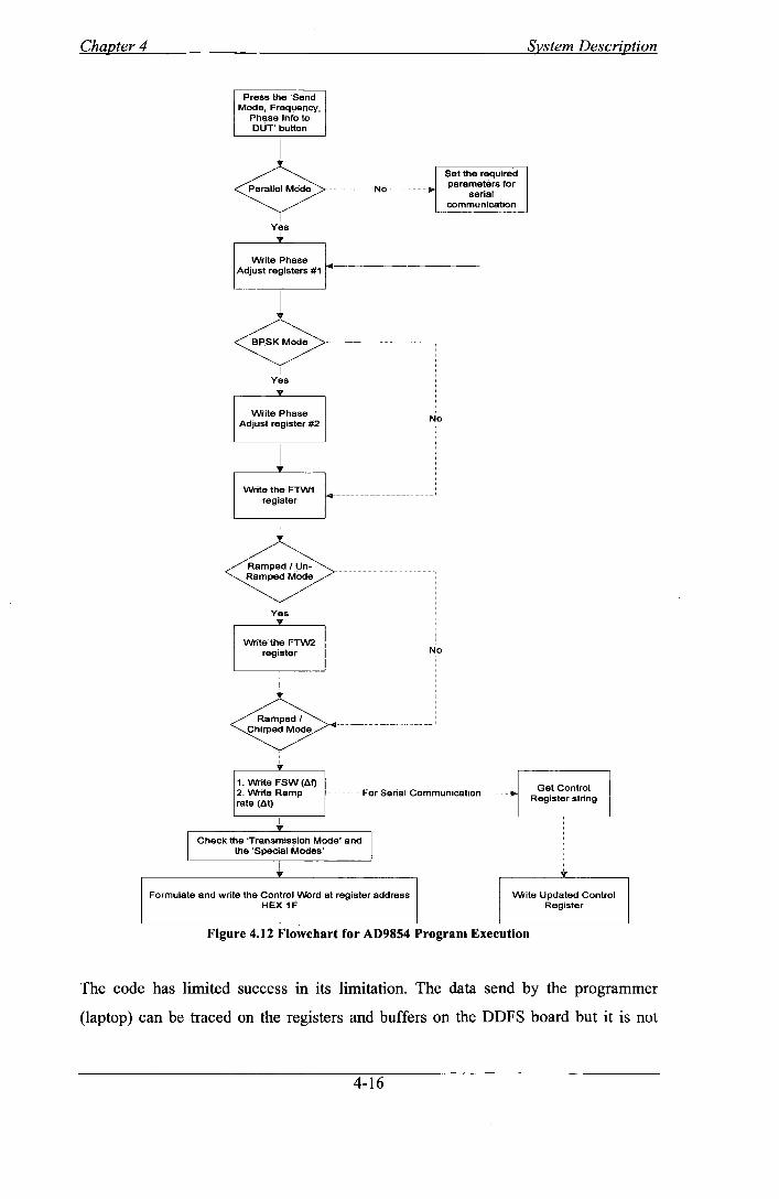
4.3.2 Digital Programmer
The digital programmer is supposed to program the DDFS board according to the
parameters selected by the user. A further task in this sweep generator is to reset the
phase after every sweep as identified in section 4.3 .1.
4-14

Chapter 4 System Description
There can be two variants to this digital programmer. One based on a 'C' program
being controlled through a PC or the other being a gate array design. Efforts were
made on both variants of the design. Both designs are explained below:-
5.3.2.1 C based Design
The 'C' code should emulate the entire program execution of the DOS AD9854. A
flowchart of the steps carried out to program the DDS board is shown in Figure 4.12.
There are three main parts to program the DDFS
• Accessing the parallel port
• Calculating the chirp parameters
• Sending appropriate data with address and control signals to program
the DDFS.
Such a 'C' language code was written using the DOS based C-compiler TC++v3. The
code listing of this is provided in A 3.1
4-15
Chapter4
Press the 'Send Mode, Frequency,
Phase lnfo to OUT' button
Yes ...
Write Phase ~ Adjust registers #1 ,~--
I
~··· i
Yes .. Write Phase
Adjust register #2
Write the FTW1 register
I Yes
....
Write the FTW2 register
i ... 1. Write FSW (.O.f)
No
No
No
Set the required parameters for
serial communication
System Description
2. Write Ramp rate (.O.t)
For Serial Communication Get Control Register string
Check tha 'Transmission Mode' and the 'Special Modes'
Formulate and write the Control Word at register address HEX 1F
I
Write Updated Control Register
Figure 4.12 Flowchart for AD9854 Program Execution
The code has limited success in its limitation. The data send by the programmer
(laptop) can be traced on the registers and buffers on the DDFS board but it is not
4-16
Chapter 4 System Description
being read by the AD9854 chip. One possible reason might be the RD (read) and WR
(write) signals. Their timing is crucial in writing any data to the chip. The code
controls these signals and is using an arbitrary 'delay' value. It has been decided that
the gate array design would be pursued to completion.
5.3.2.2 Gate Array Design
There are two variants of the Gate Array Design.
Full Extensive VHDL code design
The VHDL code was designed by another worker. The design consists of 7 functional
modules, each concerned with a specific task. Each module carries out its task in
consequence to external inputs or from one or more of the other modules. Many of the
individual block modules work but some modules and their integrated simulation are
not entirely correct.
Some reasons attributed to this are as follows:-
a. Code was previously developed for Xilinx compiler tools
b. Some commands were specific for the Xilinx FPGAs which are not
valid in Altera' s Quartus compiler
c. Some of the numerical factors used in the design are specific to the
board and the clock frequency being tested for. It was mistakenly taken
as absolute values.
4-17

Chapter 4 System Description
Keyboard Decoder _______)\
Data Translator _)\
Computation -v F1
deltaf
i N
I I
_s Z_ IIOUO
OOFS AD9854
PhaseReset CLRACC2
LED Output
WR'
I LED Display I
10 MHz
Figure 4.13 Modular Representation of Gate Array Design
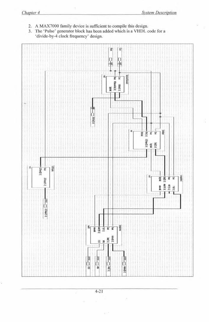
• Simpler Design (VHDL + Schematics)
Figure 4.13 shows a design that is almost in state of completion at the time of writing
this document. This gate array design consists of a mixture of VHDL code and
hardware schematics. They can be viewed in Appendices 1-2.
The modules 'keyboard decoder' , 'data translator' and ' LED Output' were designed
by another worker. They were tested successfully with the new compiler and
simulated. The two blocks 'PhaseReset' and 'Computation' were designed. They are
described as follows:-
Phase Reset Module
Name
06 MCLK
PULSE ·-··-·-·--··---··- ··-··········--······----
01
02 WRb
·-·-·--····--------IOU/0 -----·---··M1 ___________________ F.f=-f++'f'=f=~f'f-"~~f-""F~~F""~FF~F"-'-F~f'+i'+"FFF~~F
. ~~N~--L ~{~-~-~J . .r..J --~-.!. -~--~ -~--~-~-! --~-J--i-l. ~-J-~--tL.L-~-1-l.l.L.l-~.l--~-L-i.l-~--l-L.i .. Li --~-J .. Ll.l--~l-L : .J .. L M2 .L! . .)..; .. } .. d.l-~--U-U.U . .l...i..~-~--l-L; .. ;.; .. ;.t.~--!-+.!-+.d . .!..i--l-~--!-+-l--~-; .. j . .!..! .. !.j .. ! . .;..; .. ~.; .. ; . .;..L!. O_CLK i i i i i i i i i ! i ! i i i i i i ; i i : i : i ! i i i i : i ! i ! i ! i ! ! i i i ! ; ' i : i : i ' ;
···------------------- ·-:--J·r·l--r·-·r·T ·r·r·:·J··r·l--r·:·r··;·:·-l-r1·-r·:-···r·r·,-~-l-r1 ··r·r·:··r·r·r·:·-,·-~-----1·1 ·r-·:·;···-~-;·-r·:··:·i·i--:-Figure 4.14 Simulation Result: ' PhaseReset' Module
4-18

Chapter 4 System Description
The 'PhaseReset' module is designed using a hardware schematic as shown in
Appendix Al.l. Its simulation result is shown in Figure 4.14 above. The three output
signals going to the DDFS are 1/0UD, WRb and D6 (CLRACC2). The other outputs
shown in the simulation were tapped to observe the behaviour of the circuit.
Computation Module
The computation module is supposed to calculate the values required to program the
DDFS. It takes the values coming from the Data Translator module and is supposed to
output to the DDFS. The schematic is shown in A1 .2
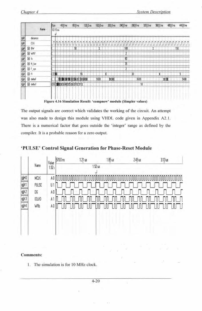
p ps 40.p ns sap ns 12010 ns 16010ns 20010 ns 24010ns 28010 ns 32010 ns 36010 ns 40010 ns 44010 ns Name [13.15ns
lt-:;--~~-anc_e _ __,! I ! ruu Arts AN I I '/ r J J.id/r{_n_r nr'i i J I J 1i iV1Wu1I!_n_m. Ar~ lfjl 1!1 BW :lU : ; ! : : , , ; ~ _!!l_w_FiF ___________ ~~~~::ti=$=F::E,:d:ti::ti=$=F::E,~E.::::=~~=F::8=Fq=t=~::S~qq::::~~
lfll 1!1 le
i l
Figure 4.15 Simulation Result. 'compnew' module (Real values)
Figure 4.15 shows the simulation result of this module when the input numerals are
actual values for the board. The zero result shows either the circuit is not working or
the values are going out of range for the present design. To check the validity of the
circuit, it was simulated for simpler values. The simulation result is shown in Fig.
4.16 below.
4-19
Chapter 4 System Description
llO.Om 120.0m 160.Dns 20D.Ons 240.Dm 280.0ns 320.0m 360.0ns 400.Dn: 440.0ns I I I I I I I I I I
Name 13.15ns .. distance
... ClK
I~ IB BW
I~ IB WRF
Figure 4.16 Simulation Result: 'compnew' module (Simpler values)
The output signals are correct which validates the working of the circuit. An attempt
was also made to design this module using VHDL code given in Appendix A2.1 .
There is a numerical factor that goes outside the 'integer' range as defined by the
compiler. It is a probable reason for a zero output.
'PULSE' Control Signal Generation for Phase-Reset Module
Value 1.21 us 1.85 us 2.49 us 3.13 us
I I I I
Name 1.521 1.52 us
MCLK AO
PULSE u 1
D6 AO
IOU ID A1
WRb AO
Comments:
1. The simulation is for 10 MHz clock.
4-20
Chapter 4 System Description
2. A MAX7000 fami ly device is sufficient to compile this design. 3. The 'Pulse' generator block has been added which is a VHDL code for a
'divide-by-4 clock frequency' design .
. . . . . . -.... . .. - ..... . -- - . . . . ..... - .. . .. . .. . - .. . . . . . . . . . . . . . . . . -. . . . . . . . . -.- .....
. . . . --.- ......... -- .. .. . . . . . . . . . . . . . . . . . . . .. . . . . - . . . . . . . . . . -.-- - . . . . . . . . . . - - . . . --.-.. . ....
. . . . . . . . . . . . . . . . . . . . . . . . . . . . . . . . - ...
. . . . . . . . . . . . --.. . ..... -...... . - . . . -- .. . . . . . . . .
. . - - - -. . . . . . -
....... . . . -- . ..
. . . . - . . . . . . . . . . . .
4-21
. . . . . . . . . - ... . .
. . - .. . . . ..... .
- .. - ... . - .... '.-
. ....... . - .... -.
- ...... . . . . . . . - . - ..... . . . . -

Chapter 4 System Description
Simulation Results
The final simulation result for the design is shown below.
114us I
6.~Ul I
To clarify the inputs and outputs, a test output "KBDecodeOut" is added to the result. The output is shown in the following figures :-
Clock
Reset
m KBINOut 00
m KBDecodeOut 14
DigitVa~d
1!1 Digit 7
valuevalid
1!1 Address 00
m Data 00
1!1 deltaF 0
lil Fl 2814 72829227009 44500:
Comments: 1. The CLK is 10 MHz. 2. The simu lated sequence from the keypad is (8,2,E),(7,5,E),(7,0,0,E) and (7,E).
This results in fc = 82 MHz, BW = 75 MHz and WRF = 700Hz. 3. The Device selected is Cyclone EP1C3T100C8
4-22
1F
86

Chapter 4 System Description
PCB Layout
Parts I Components List:
No. Device Package Value Quantity 1 Altera Cyclone TQFP100-14 EP 1 C3 T1 OOC8 1 2 10 Pin 2x5 2
Connector 3 14 Pin 2x7 3
Connector 4 8 Pin 1x8 1
Connector 5 Tri State DIP20 74244 3
Buffer 6 40 Pin- HDR40 2 2x20 1
Connector 7 Voltage T0220 LM317-1.8 1
Regulator 8 Voltage T0220 LM317-3.3 1
Regulator 9 R1 0603 1K 1
4-23

Chapter 4 System Description
10 R2,R3,R4,R5 0603 lOK 1 each 11 Cl, C2, C3, C4 0805 lOuF 1 each
4.4 References
[1] S. Davies, H. R. Holliday, "Wideband Antennas - a Historical Perspective", Ideas Engineered, Q-par Angus Ltd.
[2] Schantz, "Introduction to Ultra-wideband antennas", IEEE 2003.
[3] Analog Devices AD9854 Datasheet, pg. 26
[ 4] Printed Circuit Board Antennas - Log Periodic, Kent Electronics, http://www.wa5vjb.com/productsl.html [Last accessed: 2nd March, 2008]
[5] Musa M., Salous S., "Ambiguity Elimination in HF Radar Systems", lEE
Proceedings- Radar, Sonar Navigation, Aug. 2000, Vol. 147, No. 4, pp. 182
-188.
[6] Poole A. W. V.," Advanced sounding. The FMCW alternative", Radio
Science, December 1985, Vol. 20, No. 6, pp 1609-1619.
4-24
Chapter 5 Data Processing
Chapter 5
Data Processing
An important part of the harmonic detector is the data processing part after the
receiver. The objective of processing the data is to be able to accurately locate the
points generating harmonic frequencies. The accuracy and efficiency of the result
depends upon the technique used.
Two such methods studies so far are being described below.
5.1 Heterodyne detection
Barrick [I] has presented the technique of heterodyne detection FFT processing in his
1973 article "FM/CW Radar Signals and Digital Processing". In the 'heterodyne
detection' method, RF channel is generated locally having the same band and the
same repetition rate as that of the transmitted signal. Mixing this replica of the
transmitted signal with the received signal gives difference and sum frequencies. The
sum frequencies can be filtered out using a low pass filter. The difference frequencies,
also called as beat notes, can be used to extract the time delay and Doppler
information. The time delay will give the range and Doppler will lead to the velocity
information. The output signal is compressed and the frequency of the beat spectrum
can be on the order of a few tens of kHz. [2]
T
L-~----~--------~-L----~--L---------~~~Time
Figure 5.1 : Swept frequency versus time and the frequency of beat notes at the output of the detector.
5-1

Chapter 5 Data Processing
The mathematical expression for the transmitted chirp signal was defined in equations
(3 .1) and (3 .2). In a modified form, the transmitted and received waveform can be
represented as
Vr(t) =cos[ wJ + JrBf/] = cos~r(t)
VR(t) = AVr(t -td)
=A cos[ we (t -td) + 1rBJ, (t- td )2]
= COS ~T (t - f d )
(5.1)
(5.2)
The heterodyne mixing results in a mathematical multiplication of the two signals.
The higher frequency terms are filtered out. The beat note phase can be written as
(5.3)
where ~~ is beat or intermediate phase
t; is the internal time within the pulse
td is the delay time
After some long derivations and calculations, this beat note phase can be written as
(5.4)
where ~o is the initial phase delay corresponding to initial time delay to. This is
within a pulse i.e. the time period is
T, T, --<t<-2 2
The beat frequency is
2v h = -fc + BJ,to (5.5) c
5-2

Chapter 5 Data Processing
The first term in the above equation is due to target velocity (Doppler) and the second
term is due to delay (range) of the target.
The above equation ts valid within a pulse. For n-pulses the frequency can be
represented as
2v 2v h =-fc +Bf,to +-Bn n C C
(5.6)
5.2 Double FFT Digital Processing
Essentially two methods exist for extracting time delay (range) and Doppler shift
(velocity) channel information [3]. The first technique employs double FFT
processing; where an initial FFT is carried out over one sweep in order to extract time
delay information, and another FFT is carried out over N sweeps for each single time
delay bin in order to determine Doppler shift information. The second technique
employs a long FFT process over N sweeps in order to provide simultaneous
delay/Doppler channel information. Both techniques are identical and have the same
number of computational steps [ 1]. Here only the first technique is described in detail
as that has been studied so far. It may also be noted that for the harmonic radar
Doppler processing is not needed as the target (rusty-bolts) are not moving.
For a single transmission path, the Fourier transform over a single sweep n is
given by
T/2
v;,n (/) = J {Acos[qj1,n(t) J}e-j2Jrfidt
-T/2
(5.7)
using Euler' s definitions: cos x = ( ejx + e- jx) I 2 , sin x = ( ejx - e- jx) I 2 j , and J e'n dx
= e'n I a, equation (5.30) becomes
5-3
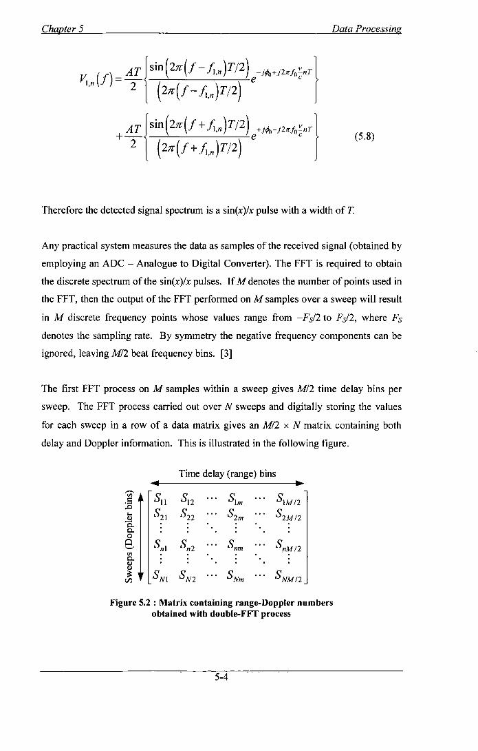
Chapter 5 Data Processing
~n(f)= AT{sin(2;r(J -J;,n)T/2) e-J~+J2trfo~nT} ' 2 ( 2n-(J- h,n )T/2)
+-- e c AT{sin(2n-(J + h,n)T/2) +J~-J2trfo~nT} 2 ( 2;r(J + h,n )T/2)
(5.8)
Therefore the detected signal spectrum is a sin(x)/x pulse with a width ofT.
Any practical system measures the data as samples ofthe received signal (obtained by
employing an ADC - Analogue to Digital Converter). The FFT is required to obtain
the discrete spectrum of the sin(x)/x pulses. If M denotes the number of points used in
the FFT, then the output of the FFT performed on M samples over a sweep will result
in M discrete frequency points whose values range from -F s/2 to F s/2, where Fs
denotes the sampling rate. By symmetry the negative frequency components can be
ignored, leaving M/2 beat frequency bins. [3]
The first FFT process on M samples within a sweep gives M/2 time delay bins per
sweep. The FFT process carried out over N sweeps and digitally storing the values
for each sweep in a row of a data matrix gives an M/2 x N matrix containing both
delay and Doppler information. This is illustrated in the following figure.
Time delay (range) bins
- SI! sl2 SI m "' SIM/2 .s .D
s21 s22 s2m s2M/2 .... 0 0.. 0.. 0
Cl sn! sn2 snm SnM/2 '-'
"' 0.. 0 0 ~ SNI SN2 SNm SNM/2 r:/)
Figure 5.2 : Matrix containing range-Doppler numbers obtained with double-FIT process
5-4
Chapter 5 Data Processing
The columns of the matrix represent the time delay bins (after the first FFT). The
elements of each column represent the digital samples of a beat frequency component
obtained every T seconds. As noted previously, for each successive sweep the
elements of the matrix columns will undoubtedly change because the beat frequency,
fi.n. and the phase term, 2;ifc( v/c)nT, are changing from sweep to sweep. The
amplitude also changes from sweep to sweep due to the minor shift in the position of
the beat note. However this change is small enough to be neglected [2]. Every sweep
takes T seconds, therefore NT seconds are required to fill the matrix shown in figure
5.2.
It can be concluded from the above that the main variations within a column
are due to the phase factor, thus
(5.9)
where 111 = NT represents the discrete time flow from sweep to sweep and K(f) is the
amplitude variation.
The Fourier transform of equation (5.9) over 111 from 0 to NT is given by
(5.10)
The above equation shows that the movement of the mobile results in a displacement
of the sin(x)/x pulse. This is known as the Doppler shift/D = (vlc)fo = viA.. [1]
5.3 SAGE Algorithm
Spatial array signal processing has emerged as an active area of research concerned
with estimating parameters from the data collected at array sensors. The estimation
5-5

Chapter 5 Data Processing
problem depends on parameters such as array geometry, sensor characteristics and
signal properties, etc. [3]. For the harmonic radar a high resolution estimation of the
DOA of received waves would give a highly accurate estimation of the location of
targets.
DOA\AOA Estimation
SAGE Algorithm
EM (ExpectationMaximisation) Algorithm
ML(Maximum Likelihood) Function
Review of other Techniques -(Parametric and Spectral-based)
DOA Problem Formulation
Linear Algebra
Figure 5.3: Hierarchy of Literature needed to be reviewed for SAGE Algorithm
r L
One such high resolution and computationally effective algorithm is the SAGE (Space
Alternating Generalized Expectation-Maximization) algorithm. This algorithm
requires a deep and thorough understanding of a variety of statistical algorithms and a
background in linear algebra. Figure (5.3) shows the kind of background required to
gain an understanding of SAGE algorithm with the help of an inverted pyramid. A
thorough understanding of the EM (Expectation-Maximisation) and ML (Maximum-
5-6

Chapter 5 Data Processing
Likelihood) techniques is needed to build upon the implementation of SAGE
algorithm. That should be the first step in SAGE Algorithm.
5-7
Chapter 5 Data Processing
5.4 References
[1] D. E. Barrick, "FM/CW Radar Signals and Digital Processing," US. Department
of Commerce, National Oceanic and Atmospheric Administration (NOAA)
Technical Report ERL 283-WPL 26, 1973.
[2] Gokalp. H, "Characterisation of UMTS FDD Channels," Ph.D. Thesis, Dept.
of Electrical Engineering and Electronics, UMIST, Manchester, UK, 2001
[3] Razavi-Ghods. N, "Characterisation of MIMO Propagation Channels", PhD.
Thesis, Dept. of Engineering, University of Durham, 2007
5-8

Chapter 6 Conclusions &Further Work
Chapter 6
Conclusions & Further Work
It can be inferred from the contents of this report that developing an advanced radar
system depends upon the knowledge of many disciplines. Several areas of research
must be integrated together to have a harmonic radar system that can effectively and
accurately locate rusty-bolt junctions. The project is multifaceted in nature and
requires a thorough understanding of various dimensions ranging from having hands
on experience to design RF hardware to having a grasp of advanced linear algebra to
implement processing algorithms. All in all, there is a real effort by the research
community to investigate and develop more efficient and accurate harmonic radar
systems as its applications find new frontiers. This is quite evident from the patents
issued in recent years as referred in the report.
The chapters in the report covered many aspects of the project. Chapter 1 introduced
the developments in radar systems and proposed a system utilizing all of these
advancements. Chapter 2 gave an overview of FMCW Harmonic radars together with
a research of NLJD (Non-Linear Junction Detectors) available in the commercial
market. Comparison with commercial products can provide valuable insight to
different aspects of this project. The radar range equation for this system needs to be
developed further. This requires the knowledge of target RCS. For the project under
discussion, some models of rusty-joints made of diodes would be used. More
information on their dimensions is required. Chapter 3 described in detail the
phenomenon of rusty-bolt effect focusing on the techniques used to identify them.
Comparing the well-known techniques with the one proposed in this project
highlights the novelty of this method. However, their performance should be
compared in terms of some measurable quantities. Chapter 4 provided a system
overview of the project and discussed its various parts focussing mainly on the digital
programmer. A significant outcome of Chapter 4 was a critical study of the work done
so far and some of the probable reasons the apparent slow progress. Chapter 5
described primarily the theoretical background of the signal processing techniques to
6-1

Chapter 6 Conclusions & Further Work
be used in the DSP block of the receiver. It highlighted the background one needs to
fully comprehend the super-resolution SAGE processing algorithm.
It should be noted that the chapters of this report only provide an elementary
description of the various systems and issues involved in developing a wide band radar
system. More detailed understanding needs to be presented for forthcoming research.
Following is a listing of possible areas of intuitive research during the course of the
project. Some of them have been indicated in the Chapter review above.
• Development of a harmonic radar range equation similar to the one being used
in entomological applications.
• RF Isolation between two receive channels which is a problem in many
commercial NLJD units.
• Comparison with other localization techniques mentioned in literature in terms
of performance and accuracy.
• Novel transmit waveform design apart from the linear chirp
a Design and development of the receiver DSP block comprising of SAGE
Algorithm. The number of antenna array 'N' in relation to the angular
resolution needs to be worked out.
System calibration and evaluation after measurements in different scenarios.
So far the approach had been to concentrate more on literature review, background
study and to develop possible hypotheses that would provide novelty to the project.
While this approach resulted in the development of some valuable premise for doing
research, it greatly effected the overall practical hardware implementation of the
project.
6-2

Appendix-] Gate Array Design - Schematics
Appendix -1 Gate Array !Design - Schematics
A1.1 Phase Reset Circuit
A digital circuit was designed that would reset the accumulated at the start of every chirp. The schematic is shown.
A-1

Date: June 27, 2008 nvgarray_new.bdf Project: nvgarray _new
'"f.i ~--L
·'"'.- - I : ,,...,.,- ..
~ r::::-:::1~· ~~1 -.---.---1 ~-ln$1J2 2CLK
fl2'''
~!?_ . .Q_F.!-~:F.,1,.9!:'~---···'
1Qr. 1QN •.
20 ' 2CN :
•''i474-
CLKI:
. . f~ ' "5C~ : :""
=t:= __ ~~"_·· __ ··········· -_· .. :; ..... ~ .... 1 --- :,~"'£ ' 7"'£ ' ~ Jj•~ ... ~~ :~:1 lOUD
"V'iRi:···
~
~~~-:~~:·~- ]
.... IQU.{i'"'"
L~i>+---f~ , .. ,., :~:
MR-
[Ill!:. Phase Reset Circuit o•e Dumam University
'""' Farrukh Aslam NJA r"' A
Suo Apr 13 22:06:59 2008 l"'"" 1 1
Page 1 of 1 Revision: nvgarray_new

Appendix-] Gate Array Design - Schematics
A1.2 Digital Controller
The digital controller schematic consists of four blocks, each written in VHDL. The controller schematic is shown below:-
A-2

Date: June 27, 2008
(a.:..:;····
;riiMi"
digitalcontroller2.bdf Project: digitalcontroller2
-~=======r======~~----~-· '----'11~·-,···:<··::· :::J····-~~:~~·I::T]·· •¥··--~~~=:.~~~~~~=~~=~:: ~ 1"1;11.!;;,-0-------'
~---~~-~--~'~-
------~~~?~~~:~_=]
;_~·.:·~-it-~_- ...
~-··ooo··
Page 1 of 1 Revision: digitalcontroller2

Appendix 2 Gate Array Design- VHDL Code
Appendix-2 Gate Array Design - VHDL Code
--Created by Farrukh Aslam -- Last Update: 05/05/08
library ieee; use ieee.std _logic _1164.all; use ieee.std _logic_ arith.all;
-- Keypad Debounce : Filters out mechanical switch bounces. Output is a clean signal typically 40ms -- De bounce clock should be approximately 1 Oms or 1OOHz entity debouncer is
port( kpb : inout std _logic_ vector (7 downto 0); clock 100Hz :in std_logic;
kpb _de bounced : in out std _logic_ vector (7 downto 0) );
end debouncer;
architecture debouncer of debouncer is
signal shift_ kpb downto 0); signal flagO, flag1, flag2, flag3 signal flag4, flagS, flag6, flag7
begin
process (clock_lOOHz) begin
:integer; :integer;
--Use of a shift register to filter switch contact bounce
------------------------------- For kpb(O) ------------------------if (clock _1 OOHz'event and clock _1OOHz=' 1 ') then
-- detect '1'
: std _logic_ vector(31
shift_ kpb(3 down to 1) <= shift_ kpb(2 down to 0); shift_ kpb(O) <= kpb (0); if shift_ kpb(3 down to 0)= "1111" then
kpb_debounced (0) <= '1'; flagO <= 1;
else kpb_debounced (0) <= '0';
end if;
A-1

Appendix 2
-- detect 101
end if;
Gate Array Design - VHDL Code
if (flagO = 1) then
end if;
shift_kpb(3 downto 1) <= shift_kpb(2 downto 0); shift_kpb(O) <= kpb (0); if shift_kpb(3 downto 0)= 11000011 then
kpb _de bounced (0) <= 101;
else kpb_debounced (0) <= 111
;
end if;
------------------------------- For kpb( 1) ------------------------
-- detect 1 1 1
-- detect 101
shift_kpb(7 downto 5) <= shift_kpb(6 downto 4); shift_kpb(4) <= kpb (1); if shift_ kpb(7 down to 4 )= 11 1111 11 then
kpb_debounced (1) <= 111;
flag1 <= 1; else
kpb _de bounced (1) <= 101;
end if;
if(flag1 = 1) then
end if;
shift_kpb(7 downto 5) <= shift_kpb(6 downto 4); shift_kpb(4) <= kpb (1); if shift_kpb(7 downto 4)= 11000011 then
kpb_debounced (1) <= 101;
else kpb_debounced (1) <= 111
;
end if;
------------------------------- For kpb(2) -------------------------- detect 1 1 1
-- detect 101
shift_kpb(11 downto 9) <= shift_kpb(lO downto 8); shift_kpb(8) <= kpb (2); if shift_ kpb( 11 down to 8)= 11 1111 11 then
kpb_debounced (2) <= 111;
flag2 <= 1; else
kpb _de bounced (2) <= 101;
end if;
if ( flag2 = 1) then shift_kpb(11 downto 9) <= shift_kpb(10 downto 8);
A-2
Appendix 2
end if;
Gate Array Design - VHDL Code
shift_ kpb(8) <= kpb (2); if shift_kpb(11 downto 8)= "0000" then
kpb _de bounced (2) <= '0'; else
kpb_debounced (2) <= '1'; end if;
------------------------------- For kpb(3) -------------------------- detect '1'
-- detect '0'
shift_kpb(15 downto 13) <= shift_kpb(14 downto 12); shift_kpb(12) <= kpb (3); if shift_kpb(15 downto 12)= "1111" then
kpb_debounced (3) <= '1'; flag3 <= 1;
else kpb_debounced (3) <= '0';
end if;
if (flag3 = 1) then
end if;
shift_kpb(15 downto 13) <= shift_kpb(14 downto 12); shift_kpb(12) <= kpb (3); if shift_kpb(15 downto 12)= "0000" then
kpb_debounced (3) <= '0'; else
kpb_debounced (3) <= '1'; end if;
------------------------------- For kpb( 4) -------------------------- detect '1'
-- detect '0'
shift_ kpb( 19 downto 17) <= shift_ kpb( 18 downto 16); shift_kpb(16) <= kpb (4); if shift_ kpb( 19 downto 16)= "1111" then
kpb_debounced (4) <= '1'; flag4 <= 1;
else kpb_debounced (4) <= '0';
end if;
if ( flag4 = 1) then shift_ kpb( 19 down to 17) <= shift_ kpb( 18 down to 16); shift_kpb(16) <= kpb (4); if shift_ kpb( 19 downto 16)= "0000" then
kpb_debounced (4) <= '0'; else
kpb_debounced (4) <= '1'; end if;
A-3
Appendix 2 Gate Array Design - VHDL Code
end if; ------------------------------- For kpb( 5) ---------------------------- detect '1'
-- detect '0'
shift_kpb(23 downto 21) <= shift_kpb(22 downto 20); shift_kpb(20) <= kpb (5); if shift_ kpb(23 down to 20 )= 11 1111 11 then
kpb _de bounced ( 5) <= '1'; flag5 <= 1;
else kpb_debounced (5) <= '0';
end if;
if ( flag5 = 1) then
end if;
shift_kpb(23 downto 21) <= shift_kpb(22 downto 20); shift_kpb(20) <= kpb (5); if shift_kpb(23 downto 20)= 11 000011 then
kpb_debounced (5) <= '0'; else
kpb_debounced (5) <= '1'; end if;
--------------------------------- For kpb( 6) ---------------------------- detect '1'
-- detect '0'
shift_kpb(27 downto 25) <= shift_kpb(26 downto 24); shift_kpb(24) <= kpb (6); if shift_ kpb(2 7 down to 24 )= 11 1111 11 then
kpb_debounced (6) <= '1'; flag6 <= 1;
else kpb_debounced (6) <= '0';
end if;
if ( flag6 = I) then
end if;
shift_kpb(27 downto 25) <= shift_kpb(26 downto 24); shift_kpb(24) <= kpb (6); if shift_ kpb(27 downto 24 )= 11 000011 then
kpb_debounced (6) <= '0'; else
kpb_debounced (6) <= '1'; end if;
--------------------------------- For kpb(7) ---------------------------- detect '1'
shift_ kpb(31 down to 29) <= shift_ kpb(30 down to 28); shift_kpb(28) <= kpb (7); if shift_ kpb(31 downto 28)= 11 1111 11 then
kpb _de bounced (7) <= '1'; flag?<= 1;
A-4
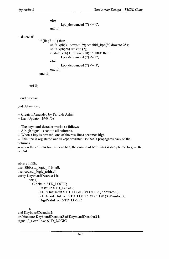
Appendix 2 Gate Array Design - VHDL Code
else kpb _de bounced (7) <= '0';
end if;
-- detect '0' if(flag7 = 1) then
shift_ kpb(31 down to 29) <= shift_ kpb(30 down to 28); shift_ kpb(28) <= kpb (7); if shift_ kpb(31 downto 28)= "0000" then
kpb_debounced (7) <= '0'; else
kpb_debounced (7) <= '1'; end if;
end if;
end if;
end process;
end debouncer;
--Created/Amended by Farrukh Aslam -- Last Update : 29/04/08
-- The keyboard decoder works as follows: -- A high signal is sent to all columns. -- When a key is pressed, one of the row lines becomes high -- This line is registered and is kept presistent so that is propagates back to the columns --when the column line is identified, the combo ofboth lines is deciphered to give the ouptut
library IEEE; use IEEE.std _logic _1164.all; use ieee.std_logic_arith.all; entity KeyboardDecoder2 is
port ( Clock: in STD_LOGIC;
Reset: in STD_ LOGIC; KBinOut: inout STD LOGIC VECTOR (7 downto 0); - -KBDecodeOut: out STD LOGIC VECTOR (3 downto 0); - -DigitValid: out STD_LOGIC
); end KeyboardDecoder2; architecture KeyboardDecoder2 of KeyboardDecoder2 is signal S_ScanRow: STD_LOGIC;
A-5

Appendix 2 Gate Array Design - VHDL Code
signal S_ScanCol: STD_LOGIC; signal S_PulseCounter: INTEGER; signal S _ ResetFlag: INTEGER; signal S_KBinOut: STD_LOGIC_ VECTOR(? downto 0); signal S_KBinRow: STD_LOGIC_ VECTOR(3 downto 0); signal S_KBinCol: STD_LOGIC_ VECTOR(3 downto 0); signal S_KBOutRow: STD_LOGIC_ VECTOR(3 downto 0); signal S_KBOutCol: STD_LOGIC_ VECTOR(3 downto 0);
begin
-- First four lines of KBinOut are connected as rows on the keyboard and the last four lines -- as columns. The condition is a default condition set by the reset line and when no key is --pressed.
S_KBinRow<=KBin0ut(3 downto 0) when (S_ScanRow='l' and S_ScanCol='O') else ( others=>'Z'); KBin0ut(7 downto 4)<=S_KBOutCol when (S_ScanRow='l' and S_ScanCol='O') else ( others=>'Z'); KBin0ut(3 downto O)<=S_KBOutRow when (S_ScanCol='l' and S_ScanRow='O') else ( others=>'Z'); S_KBinCol<=KBinOut(7 downto 4) when (S_ScanCol='l' and S_ScanRow='O') else ( others=>'Z');
process(Reset,Clock) begin
if;
if(Reset='l') then S _ KBOutCol<=( others=>' I'); S ScanRow<='I'·
- ' S _ ScanCol<='O'; S _ ResetFlag<= 1; S _ PulseCounter<=O;
elsif(Clock'Event and Clock=' I') then if(S _ ScanRow='l' and S _ ScanCol='O') then
if(S_ResetFlag=O) then S _ PulseCounter<=S _ PulseCounter+ 1 ;
end if; DigitValid<='O';
if(S _ PulseCounter> 3 and S _ PulseCounter<5) then if(S _ PulseCounter= 1) then
DigitValid<='l'; else
DigitValid<='O'; end if; if(S_PulseCounter>5) then S_PulseCounter<=6; end
if((S_KBinRow/="ZZZZ") and (S_KBinRow>"OOOO")) then
A-6

Appendix 2
end if;
Gate Array Design - VHDL Code
S_KBin0ut(3 downto O)<=S_KBinRow; S _ KBOutRow<=S _ KBinRow; S _ ScanRow<='O'; S _Scan Col<=' 1 ';
elsif(S _ ScanRow='O' and S _ ScanCol=' 1 ') then S _ PulseCounter<=O; if((S_KBinCol/=11ZZZZ11
) and (S_KBinCol>11 000011)) then--
remember to set KBin pulled down
end if;
S_KBin0ut(7 downto 4)<=S_KBinCol; S _ ScanRow<='O'; S ScanCol<='O'·
- ' S _ ResetFlag<=O;
elsif(S _ ScanRow='O' and S _ ScanCol='O') then S _ PulseCounter<=O;
-- The 1 's in the KBinOut are basically shorted out pins coming from the keyboard decoder after -- pressing of any key.
if(S_KBin0ut=11 00010001 11) then
KBDecodeOut<=11 000011; --0
elsif(S_KBin0ut=1100100001 11) then
KBDecode0ut<=11 0001 11; --1
elsif(S _ KBinOut=110 1000001 11) then
KBDecode0ut<=11 00 1011; --2
elsif(S _ KBin0ut=11 10000001 11) then
KBDecode0ut<=11 0011 11; --3
elsif(S_KBin0ut=110001001011) then
KBDecode0ut<=11 010011; --4
elsif(S _ KBinOut=1100 10001 011) then
KBDecode0ut<=11 0 101 11; --5
elsif(S _ KBin0ut=110 100001 011) then
KBDecodeOut<=11 011011; --6
elsif(S _ KBinOut=11 1000001 011) then
KBDecode0ut<=11 0 111 11; --7
elsif(S _ KBin0ut=11000 101 0011) then
KBDecode0ut<=11 100011; --8
elsif(S_KBin0ut=11 0010010011) then
KBDecodeOut<=11 1001 11; --9
elsif(S _ KBin0ut=11 0 10001 0011) then
KBDecode0ut<=11 101011; --a
elsif(S _ KBin0ut=11 100001 0011) then
KBDecode0ut<=11 1011 11; --b
elsif(S_KBinOut=11 0001100011) then
KBDecode0ut<=11 110011; --c
elsif(S _ KBin0ut=11 00 101 00011) then
KBDecode0ut<=11 1101 11; --d
elsif(S _ KBinOut=11 0 1001 00011) then
KBDecode0ut<=11 111011; --e
A-7

Appendix 2 Gate Array Design - VHDL Code
elsif(S_KBinOut=" 10001000") then KBDecodeOut<=" 1111 "; --f
end if;
DigitValid<='1';
S _ KBOutCol<=( others=>'1'); S ScanRow<='1'·
- '
end if; end if;
end process;
S ScanCol<='O'· - '
end KeyboardDecoder2;
Created/ Amended by Farrukh Aslam Last Update: 06/05/08
-- This block formulates a number for the computation block. It detects if a number or a letter -- key has been pressed. So far actions are only taken on a number key and the 'E' and 'C' keys. -- It also ouptuts to the LEDs displaying the keys that have been pressed.
library IEEE; use IEEE.std_logic_1164.all; use IEEE.std _logic_ unsigned.all; use IEEE.std _logic_ arith.all;
entity datainput_ new is port (
Clock: in STD_ LOGIC; Reset: in STD_ LOGIC; KBin: in STD_LOGIC_ VECTOR (3 downto 0); KBinValid: in STD_LOGIC; Digit: out STD_ LOGIC_ VECTOR (23 downto 0); DigitValid: out STD_LOGIC; LEDOutput: out STD_LOGIC_ VECTOR (11 downto 0) );
end datainput_ new;
architecture datainput_ new of datainput_ new is
signal S_Digit: STD_LOGIC_ VECTOR (23 downto 0); signal I_Chunkl: INTEGER; signal I_Chunk2: INTEGER; signal I_ Chunk3: INTEGER; signal I_Chunk4: INTEGER; signal I_Chunk5: INTEGER; signal I_Chunk6: INTEGER; signal I_Total: INTEGER;
A-8

Appendix 2 Gate Array Design - VHDL Code
signal KBinO, KBin1, KBin2: std_logic_vector (3 downto 0); signal flagO, flag 1, flag2 : integer;
begin
process (Reset,Clock,KBinValid) begin
if(Reset='l') then DigitValid<='O'; flagO <= 1; flag1 <= 0; flag2 <= 0;
Digit<=(Others=>'O');
S _Digit<=( Others=>'1'); I_Chunk1<=0; I_Chunk2<=0;
I_Chunk4<=0; I_ Chunk6<=0;
I Chunk3<=0· - '
I_ Chunk5<=0; I_Total<=O;
elsif(Clock'Event and Clock='1') then DigitValid<='O';
if(KBin V alid='1') then if(KBin<"1010") then
I_ Chunk6<=I _ChunkS; I_ Chunk5<=I_ Chunk4;
I_ Chunk4<=I _ Chunk3; I_ Chunk3<=1 _ Chunk2;
I_Chunk2<=I_Chunk1; I_ Chunk1 <=CONV _ INTEGER(KBin);
S_Digit(23 downto 20)<=S_Digit(19 downto 16);
S_Digit(19 downto 16)<=S_Digit(15 downto 12); S_Digit(15 downto 12)<=S_Digit(11 downto 8);
S_Digit(11 downto 8)<=S_Digit(7 downto 4); S_Digit(7 downto 4)<=S_Digit(3 downto 0); S_Digit(3 downto O)<=KBin;
--------------------------- LEDOutput ----------------------------if ( flagO = 1) then KBinO <= KBin; LEDOutput (11 downto 8) <= KBinO; LEDOutput (7 downto 4) <= x"O"; LEDOutput (3 downto 0) <= x"O"; flagO <= 0; end if;
if (flagO = 0) then
A-9

Appendix 2 Gate Array Design - VHDL Code
KBin1 <= KBin; LEDOutput (11 downto 8) <= KBinO ; LEDOutput (7 downto 4) <= KBin1; LEDOutput (3 downto 0) <= x"O"; flag1 <= 1; end if;
elsif(KBin=" 11 00") then --- clear the input digit S _ Digit(23 down to O)<=(Others=>' 1 '); I_Chunk1 <=0; I_Chunk2<=0; I_Chunk3<=0; I_Chunk4<=0; I_Chunk5<=0; I_Chunk6<=0;
elsif(KBin=" 111 0") then --- enterkey S _ Digit(23 downto O)<=(Others=>' 1 ');
I Total<=! Chunkl+I Chunk2*10+1 Chunk3*100+ - - - -
I_ Chunk4 * 1 000+1 _ Chunk5* 1 0000+1 _ Chunk6* 1 00000; I_Chunk1<=0; I_Chunk2<=0;
I_Chunk4<=0; I_ Chunk6<=0;
I_ Chunk3<=0; I_ Chunk5<=0;
-- LEDOutput after 'Enter' key
end if;
if (flag1 = 1) then KBin2 <= KBin; LEDOutput (11 downto 8) <= KBinO; LEDOutput (7 downto 4) <= KBin1 ; LEDOutput (3 downto 0) <= KBin2 ; flagO <= 1; end if;
elsif(I _ Total>O) then
end if; end process; End datainput_ new;
Digit<=CONV _STD _LOGIC_ VECTOR(I_Total,24); I_Total<=O; DigitValid<='1 ';
end if;
A-10

Appendix 2 Gate Array Design - VHDL Code
-- created by Farrukh Aslam -- Last Update: 29th April 2008
library IEEE; use IEEE.std_logic_ll64.all;
entity LEDDisplay is port (
Reset: in STD_LOGIC; LEDinput: in STD_LOGIC_ VECTOR (23 downto 0); LEDOutput: out STD_LOGIC_ VECTOR (11 downto 0) );
end LEDDisplay; architecture LEDDisplay ofLEDDisplay is begin
process (LEDinput) begin
0)<="0111 ";
0)<="0100";
0)<="1101";
0)<="1101";
0)<=" 111 0";
0)<="1011";
0)<=" 1011 ";
0)<="0101 ";
0)<=" 1111 ";
0)<="1111";
0)<="1100";
0)<="0011 ";
0)<=" 1111 ";
4)<="0111 ";
LEDOutput<=(Others=>'O'); if(LEDinput(3 downto 0)="0000") then LEDOutput(3 downto
elsif(LED1nput(3 downto 0)="0001 ")then LED0utput(3 downto
elsif(LEDinput(3 downto 0)="0010") then LED0utput(3 downto
elsif(LEDinput(3 downto 0)="0011 ")then LEDOutput(3 downto
elsif(LEDinput(3 downto 0)="0100") then LEDOutput(3 downto
elsif(LEDinput(3 downto 0)="0101 ")then LEDOutput(3 downto
elsif(LEDinput(3 downto 0)="0 11 0") then LEDOutput(3 downto
elsif(LEDinput(3 downto 0)="0111 ")then LEDOutput(3 downto
elsif(LEDinput(3 downto 0)="1000") then LEDOutput(3 downto
elsif(LEDinput(3 downto 0)="1001 ")then LED0utput(3 downto
elsif(LEDinput(3 down to 0)=" 1101 ") then LED0utput(3 down to
elsif(LEDinput(3 down to 0)=" 11 00") then LED0utput(3 down to
elsif(LEDinput(3 downto 0)=" 1001 ")then LED0utput(3 downto
else LED0utput(11 downto 0)<="000000000000"; end if; if(LEDinput(7 downto 4)="0000") then LEDOutput(7 downto
A-ll

Appendix 2
4)<="0100";
4)<="1101";
4)<="1101 ";
4)<="1110";
4)<="1011 ";
4)<="1011 ";
4)<="0101 ";
4 )<=11 1111 ";
4 )<=" 1111 11;
Gate Array Design - VHDL Code
elsif(LED1nput(7 down to 4)="000 1 ") then LED0utput(7 downto
elsif(LEDinput(7 downto 4)="0010") then LEDOutput(7 downto
elsif(LEDinput(7 downto 4)="0011 ")then LED0utput(7 downto
elsif(LEDinput(7 downto 4)="0100") then LEDOutput(7 downto
elsif(LEDinput(7 downto 4)="0101 ")then LEDOutput(7 downto
elsif(LEDinput(7 downto 4)="0110") then LEDOutput(7 downto
elsif(LEDinput(7 downto 4)="0111 ")then LEDOutput(7 downto
elsif(LEDinput(7 downto 4 )=" 1 000") then LED0utput(7 downto
elsif(LEDinput(7 downto 4)=" 1001 ")then LEDOutput(7 downto
else LEDOutput(11 downto 0)<="000000000000"; end if; if(LED1nput(11 downto 8)=110000") then LEDOutput(11
downto 8)<=11 0111 ";
8)<="0100";
8)<=11 1101 11;
8)<="1101 ";
8)<=11 111011;
8)<=11 1011 11;
8)<=11 1011 11;
8)<=11 0101 ";
8)<=" 1111 11;
8)<=" 1111 ";
end process;
elsif(LEDinput( 11 down to 8)="000 1 ") then LEDOutput( 11 down to
elsif(LED1nput(11 downto 8)="0010") then LEDOutput(11 downto
elsif(LEDinput(11 downto 8)="0011 ")then LEDOutput(11 downto
elsif(LEDinput(11 downto 8)="0100") then LED0utput(11 downto
elsif(LEDinput(11 downto 8)="0101 ")then LEDOutput(11 downto
elsif(LEDinput(11 downto 8)="0110") then LEDOutput(11 downto
elsif(LEDinput(11 downto 8)=11 0111 11) then LEDOutput(11 downto
elsif(LEDinput(11 downto 8)=11 1000") then LEDOutput(11 downto
elsif(LEDinput(11 downto 8)=11 1001 11) then LEDOutput(11 down to
else LEDOutput(11 downto 0)<="000000000000"; end if;
end LEDDisplay;
A-12

Appendix 2 Gate Array Design - VHDL Code
--created by Farrukh Aslam --Last Update: 14/04/08
-- This block computes the values needed to be programmed in the DDFS synthesizer. --The order of values being entered is fc, BW, WRF. The factor (2/\48/SysClk) remains -- to be added.
library IEEE; use IEEE.std _logic _1164.all; use IEEE.std_logic_arith.all; use IEEE. std _logic_ unsigned.all; --use IEEE.math_real.all; --use IEEE. numeric_ std.all; entity computation2 is
port ( Clock: in STD_ LOGIC;
Reset: in STD_ LOGIC; Digit: in STD_ LOGIC_ VECTOR (23 down to 0); DigitValid: in STD_LOGIC;
F1: out STD_LOGIC_ VECTOR (47 downto 0); FC: out STD_LOGIC_ VECTOR (47 downto 0); WRF: out STD_LOGIC_ VECTOR (15 downto 0); BW: out STD_LOGIC_ VECTOR (47 downto 0); deltaF: out STD_LOGIC_ VECTOR(47 downto 0);
valuevalid: out std_logic ; F1_factor: out STD_LOGIC_ VECTOR (47 downto 0)
factor_bin: out std_logic_vector (19 downto 0)
); end computation2;
architecture computation2 of computation2 is signal I_ WordNumber:INTEGER;
signal I_FC: INTEGER; signal I_BW:INTEGER; signal I_ WRF:INTEGER; signal I_F1 :INTEGER; signal I_DF:INTEGER;
--signal counter:INTEGER;
--signal I_FC: unsigned (1 downto 0); --signal I_BW: unsigned (1 downto 0);
A-13

Appendix 2
--signal I_ WRF:unsigned (1 downto 0); --signal I_F1 :unsigned (1 downto 0); --signal I_DF:unsigned (1 downto 0);
--signal I_F11: unsigned; --signal F 1_ factor: real;
--constant x: unsigned ( 1 downto 0) := b"O 1" ; --constant y: unsigned (1 downto 0) := b"OO"; --constant z: unsigned (11 downto 0) := X"3E8";
--constant a: unsigned (1 downto 0) := b"lO";
signal factor : real ;
begin
factor<= (2.0E10) I 3.0E3 ; factor_bin <= conv_std_logic_vector (factor,20);
process (DigitValid,Reset) begin
if (reset=' 1 ') then I_ WordNumber <=1; I_BW <=0; I_WRF<=O; I_FC <= 0; I DF<= O· - '
valuevalid<= '0';
--I_F11 <= to_unsigned (I_F1,48 );
Gate Array Design - VHDL Code
elsif (DigitValid'Event and DigitValid='O') then if(I_WordNumber=1)then
I_FC <=CONY _INTEGER (Digit); --I_FC <= unsigned (Digit); I_ WordNumber<=2;
elsif(I _ WordNumber=2) then I FC <=I FC * 1000· - - ' --I FC <=I FC * z · - - ' I BW <= CONY INTEGER (Digit); - -I_ WordNumber<=3;
elsif(I_ WordNumber=3) then --I BW <= I BW * z·
- - '
A-14

Appendix 2
end if;
Gate Array Design - VHDL Code
I_BW <= I_BW * 1000; I_ WRF<= CONV _INTEGER (Digit);
I_ WordNumber<=4;
elsif (I_ WordNumber<=4) then I_F1 <= I_FC- (I_BW I 2);
I_DF <= ((I_BW *I_ WRF) I 300000) * 114;
valuevalid <= '1 '; --x <= round (2.0E1);
end if;
F1 <= CONV ~STD_LOGIC_ VECTOR (I_F1, 48); --FC <= CONV _STD _LOGIC_ VECTOR (I_FC, 48); --BW <= CONV _STD_LOGIC_ VECTOR (I_BW, 48); WRF<= CONV _STD_LOGIC_ VECTOR (I_ WRF, 16); deltaF <= CONV_STD_LOGIC_ VECTOR (I_DF, 48);
--F1_factor <= CONV _STD_LOGIC_ VECTOR (x, 48);
end process;
end computation2;
-- DDFS AD9854 Programmer -- created by Farrukh Aslam -- Last Update : 14104108
--This block transmits the values ofFl, deltaF, ramp rate, RetMult and the control word --to AD9854. It also generates signals for WRb and the lOUD Clk.
library IEEE; use IEEE.std_logic_1164.all; use IEEE.std _logic_ arith.all; use IEEE.std _logic_ unsigned. all;
entity programmer is port (
Reset: in STD_LOGIC; Clock: in STD_ LOGIC ; Fl :in STD_LOGIC_ VECTOR (47 downto 0); deltaF: in STD_LOGIC_ VECTOR (47 downto 0); valuevalid : in std _logic;
Address: out STD_LOGIC_ VECTOR (5 downto 0);
A-15
Appendix 2 Gate Array Design - VHDL Code
Data : out STD_ LOGIC_ VECTOR (7 down to 0); WRb: out std_logic; lOUD : out std _logic
--dfcount: out std_logic );
end programmer;
architecture programmer of programmer is signal clk_s: std_logic; signal syncon: std_logic; signal counter: integer; signal count : integer; signal dfcounter: integer; signal start 1 : integer; signal rrcounter: integer; signal rcount: integer; signal rmcounter: integer; signal cwcounter: integer;
signal buffD: std _logic; signal buffl: std _logic; signal WRs: std_logic;
signal fregO : STD_ LOGIC_ VECTOR (7 downto 0); signal fregl : STD_LOGIC_ VECTOR (7 downto 0); signal freg2 : STD_ LOGIC_ VECTOR (7 downto 0); signal freg3 : STD_ LOGIC_ VECTOR (7 down to 0); signal freg4 : STD_ LOGIC_ VECTOR (7 downto 0); signal freg5 : STD_ LOGIC_ VECTOR (7 downto 0);
signal dfregO: STD_LOGIC_ VECTOR (7 downto 0); signal dfregl : STD_LOGIC_ VECTOR (7 downto 0); signal dfreg2 : STD_ LOGIC_ VECTOR (7 downto 0); signal dfreg3 : STD _LOGIC_ VECTOR (7 downto 0); signal dfreg4: STD_LOGIC_ VECTOR (7 downto 0); signal dfreg5 : STD_ LOGIC_ VECTOR (7 downto 0);
begin
fregO <= Fl (47 downto 40); freg1 <= Fl (39 downto 32); freg2 <= F1 (31 downto 24); freg3 <= Fl (23 downto 16); freg4 <= Fl (15 downto 8); freg5 <= Fl (7 downto 0);
A-16
Appendix 2
dfregO <= deltaF (47 downto 40); dfreg1 <= deltaF (39 downto 32); dfreg2 <= deltaF (31 downto 24); dfreg3 <= deltaF (23 downto 16); dfreg4 <= deltaF (15 downto 8); dfreg5 <= deltaF (7 downto 0);
syncon_gen: process(Clock) begin
if (Clock'event and Clock= '1 ')then clk_s <=not (clk_s); syncon<=clk _ s;
end if; end process syncon _gen ;
-- Reset Initialization init: process (Clock, Reset) begin
if (Reset =' 1 ') then start1 <=0;
elsif (valuevalid = '1 ')then
start1<=1;
end if;
end process init;
--Tranmission of WRb _gen WTbgen: process(Clock) begin
if (Clock'Event and Clock='1 ')then --buffO <=not (Clock);
end if;
--buffl <=buffD; WRs <=not (WRs); WRb <=WRs;
end process wrbgen;
-- Transmission of lOUD Clock IOUD<=WRs;
-- Process to send data to AD9854 prog: process (syncon, Reset) begin
if (Reset=' 1 ') then counter<=O; count<=O;
A-17
Gate Array Design - VHDL Code
Appendix 2
Address<=b"OOOOOO"; Data <=b"OOOOOOOO"; WRb<='l'; IOUD<='O'; dfcounter<=O; rrcounter<=O; rcount<=O; rmcounter<=O; cwcounter<=O;
Gate Array Design - VHDL Code
---- Transmission ofF 1 words elsif (syncon'Event and syncon='l ')then
if( counter=O and start1 = 1) then
Address <= b"000100"; Data <= fregO; counter<= 1;
elsif( counter= 1 and start1 = 1) then
Address <= b"000101 "; Data <= fregl; counter <=2;
elsif(counter=2 and start1=1) then
Address <= b"000110"; Data <= freg2; counter <=3;
elsif( counter=3 and start!= 1) then
Address <= b"000111 "; Data<= freg3; counter<=4;
elsif( counter=4 and start 1 = 1) then
Address <= b"001000"; Data<= freg4; counter<=S;
elsif( counter=S and start1 = 1) then
end if;
Address <= b"001001 "; Data<= freg5; dfcounter<= 1;
A-18

Appendix 2 Gate Array Design - VHDL Code
---- Transmission of detiaF words if( count=O and dfcounter= 1) then
Address <= b"001010"; Data <= dfregO; count<=1;
eisif( count= I and dfcounter= 1) then Address <= b"0010I1 "; Data<= dfreg1; count <=2;
e1sif( count=2 and dfcounter= 1) then
Address <= b"001100"; Data <= dfreg2; count <=3;
elsif( count=3 and dfcounter= I) then
Address <= b"001101 "; Data <= dfreg3; count<=4;
elsif( count=4 and dfcounter= 1) then
Address <= b"001110"; Data <= dfreg4; count<=5;
elsif( count=5 and dfcounter= 1) then
end if;
Address <= b"001111 "; Data<= dfreg5; rrcounter<= 1;
-- Tranmission of ramp rate clock
if(rcount=O and rrcounter=1) then Address <= b"011010"; Data<= b"OOOOOOOO"; rcount<=1;
elsif(rcount=1 and rrcounter=1) then
Address <=b"011011"; Data<= b"OOOOOOOO"; rcount <=2;
A-19

Appendix 2 Gate Array Design - VHDL Code
elsif(rcount=2 and rrcounter=1) then
end if;
Address <= b"011100"; Data<= b"01110001"; rmcounter<= 1;
--Tranmission of RefMult values if(rmcounter=1) then
end if;
Address <= b"011110"; Data<= b"01001111"; cwcounter<= 1;
--Tranmission of Control Word
end if;
end process prog;
end programmer;
if( cwcounter= 1) then Address <= b"011111"; Data<= b"10000110";
end if;
A-20
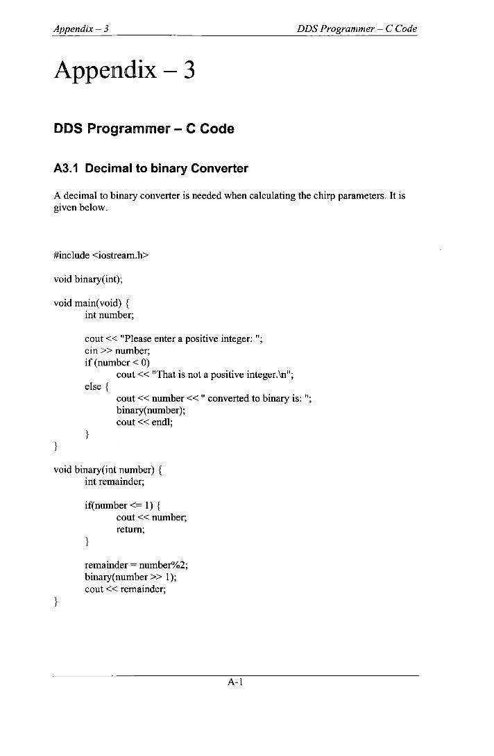
Appendix- 3 DDS Programmer- C Code
Appendix- 3
DOS Programmer- C Code
A3.1 Decimal to binary Converter
A decimal to binary converter is needed when calculating the chirp parameters. It is given below.
#include <iostream.h>
void binary(int);
void main( void) { int number;
cout <<"Please enter a positive integer: "; cin >>number;
}
if (number< 0)
else {
}
cout <<"That is not a positive integer.\n";
cout <<number<<" converted to binary is:"; binary( number); cout << endl;
void binary(int number) { int remainder;
}
if(number <= 1) {
}
cout <<number; return;
remainder = number%2; binary( number>> 1 ); cout <<remainder;
A-1

, f
Appendix- 3 DDS Programmer- C Code
A3.2 Programming the DDFS
A C code was written that would take values from user, calculate the required parameters and then send data to the DDFS board.
I/ chirp.cpp: Defines the entry point for the console application.
#include <stdio.h> #include <dos.h> #include <iostream.h> #include <conio.h>
#define DATAPORT OX3BC #define STATUSPORT DATAPORT + 1 #define CTRLPORT DATAPORT + 2
void cmdloadPLL _click ( unsigned long refrnul); void cmdloadUDCLK_click (unsigned long UDCLK); void cm dAmp Load_ click(); void cmdLoad_click (unsigned long FTW, unsigned long FSW, unsigned long Ramprate); void cmdLoad _click_ test();
void write (int address , int data); void writedata (int data); void writeaddr (int addr); void WRBAR _lo (); void WRBAR _hi (); void latchdata (); void latchaddr (); void latchctrl ();
unsigned long extclk, refrnul, FTW, FSW, Ramprate; unsigned long F _ sys, UDCLK;
void main() {
/* clrscr();
printf ("Enter the external clock frequency: "); scanf ("%d", &extclk);
printf ("\nEnter the system reference multiplier value:"); scanf ("%d", &refrnul);
printf ("\nEnter the system I/0 UD CLK frequency:"); scanf ("%d", &UDCLK);
F _ sys = refmul * extclk;
A-2

Appendix- 3 DDS Programmer- C Code
cout << "\n Value ofF _sys:" << F _sys; *I
cout <<"Enter to start:"; cmdloadPLL_click(refmul); //Load the Reference multiplier value in
the register value 1 E
cmdloadUDCLK_click (UDCLK); //Load the UDCLK value in the registers 16, 1 7, 18, 19
I/ cm dAmp Load_ click();
/* printf ("Enter the Start frequency:"); scanf ("%d", &FTW);
printf ("\nEnter Frequency Step Word:"); scanf ("%d", &FSW);
printf ("\nEnter the Ramp rate:" , "\n"); scanf("%d", &Ramprate); *I
11 Load 0 value at IF
//cmdLoad_click (FTW, FSW, Ramprate); //Load FTW, FSW, Ramprate and Control word register
}
cmdLoad_click_test (); cout <<"Finished!"; getch();
void cmdloadPLL _click ( unsigned long refmul) {
/* int Intval = 64 + refmul; write (30, Intval);
*I write (30,0x46);
}
void cmdloadUDCLK_click (unsigned long UDCLK) {
unsigned long N; int UDl, UD2, UD3, UD4; /*N = (F _sys I (UDCLK*2))- 1 ; //printf("\n Value ofN is:", '%d', 'N'); //cout <<"Value ofN is: " << N;
UD 1 = N & OxFFOOOOOO; UD2 = N & OxFFOOOO; UD3 = N & OxFFOO; UD4 = N & OxFF;
A-3

Appendix- 3
}
write (16, UD1); write (17, UD2); write (18, UD3); write (19, UD4); *I flint Intval = 3; If For Chirp mode //Intval = Intval + 1; //For Internal Clock
//write (Ox1F,Intval); write (Oxl6,0x00); write (Ox17,0xOB); write (Ox18,0x71); write (Ox19,0xAF);
void cmdAmpLoad _click() {
int Intval = 0; write (Intval, Ox1F);
} /*
DDS Programmer- C Code
void cmdLoad_click (unsigned long FTW, unsigned long FSW, unsigned long Ramprate) {
int FTW1, FTW2, FTW3, FTW4, FTW5, FTW6; int FSW1, FSW2, FSW3, FSW4, FSW5, FSW6; int Ramprate1, Ramprate2, Ramprate3;
//Use the default values of phase registers is 00. I/ Separate FTW bytes and write in corresponding registers FTW1 = FTW & OxFFOOOOOOOOOO; FTW2 = FTW & OxFFOOOOOOOO; FTW3 = FTW & OxFFOOOOOO; FTW 4 = FTW & OxFFOOOO; FTW5 = FTW & OxFFOO; FTW6 =FTW &OxFF;
write (Ox04, FTW1); write (Ox05, FTW2); write (Ox06, FTW3); write (Ox07, FTW4); write (Ox08, FTW5); write (Ox09, FTW6);
A-4

Appendix- 3 DDS Programmer- C Code
} */
/I Separate FSW bytes and write in corresponding registers FSWl = FSW & OxFFOOOOOOOOOO; FSW2 = FSW & OxFFOOOOOOOO; FSW3 = FSW & OxFFOOOOOO; FSW 4 = FSW & OxFFOOOO; FSW5 = FSW & OxFFOO; FSW6 = FSW & OxFF;
write (OxlO, FSWl); write (Oxll, FSW2); write (Ox12, FSW3); write (Ox13, FSW4); write (Ox14, FSW5); write (Oxl5, FSW6);
I/ Separate Ramprate registers and write in corresponding registers
Ram prate 1 = Ramprate & OxFFOOOO; Ramprate2 = Ramprate & OxFFOO; Ramprate3 = Ramprate & OxFF;
write (OxlA, Rampratel); write (OxlB, Ramprate2); write (OxlC, Ramprate3);
write (OxlF, Ox87); I/ Write the control word for chip generation at lF
void cmdLoad _click_ test () {
//write FTWl write (Ox04, Ox08); write (Ox05, Ox88); write (Ox06, Ox88); write (Ox07, Ox88); write (Ox08, Ox88); write (Ox09, Ox88);
//write FSW write (OxlO, OxOO); write (Oxll, Ox02); write (Oxl2, Ox2F); write (Oxl3, Ox3E); write (Oxl4, Ox93); write (Ox15, Ox97);
//write Ramprate write (OxlA, OxOO);
A-5
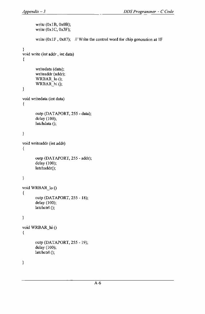
Appendix- 3
write (OxlB, OxOB); write (OxlC, Ox3F);
DDS Programmer- C Code
write (OxlF, Ox87); I/ Write the control word for chip generation at IF
} void write (int addr , int data) {
}
writedata (data); writeaddr (addr); WRBAR_lo(); WRBAR_hi ();
void writedata (int data) {
}
outp (DATAPORT, 255- data); delay (1 00); latchdata ();
void writeaddr (int addr) {
}
outp (DATAPORT, 255- addr); delay (100); latchaddr();
void WRBAR_lo () {
}
outp (DATAPORT, 255- 18); delay (1 00); latchctrl ();
void WRBAR _hi () {
}
outp (DATAPORT, 255- 19); delay (1 00); latchctrl ();
A-6

Appendix- 3
write (Ox1B, OxOB); write (OxlC, Ox3F);
DDS Programmer- C Code
write (Ox1F, Ox87); I/ Write the control word for chip generation at 1F
} void write (int addr, int data) {
}
writedata (data); writeaddr (addr); WRBAR_lo (); WRBAR_hi ();
void writedata (int data) {
}
outp (DATAPORT, 255- data); delay (100); latchdata ();
void writeaddr (int addr) {
}
outp (DATAPORT, 255- addr); delay (100); latchaddr();
void WRBAR_lo () {
}
outp (DATAPORT, 255- 18); delay (1 00); latchctrl ();
void WRBAR _hi () {
}
outp (DATAPORT, 255- 19); delay (100); latchctrl ();
A-6

Appendix- 3
void latchdata () {
}
outp (CTRLPORT, 10); delay (100); outp (CTRLPORT, 11); delay (100);
void latchaddr () {
}
outp (CTRLPORT, 9); delay (100); outp (CTRLPORT, 11); delay (100);
void latchctrl () {
}
outp (CTRLPORT, 3); delay (100); outp (CTRLPORT, 11); delay (100);
DDS Programmer- C Code
A-7
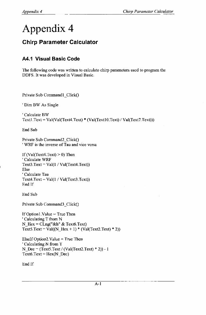
Appendix 4 Chirp Parameter Calculator
Appendix 4 Chirp Parameter Calculator
A4.1 Visual Basic Code
The following code was written to calculate chirp parameters used to program the DDFS. It was developed in Visual Basic.
Private Sub Commandl_Click()
1 Dim BW As Single
1 Calculate BW Textl.Text = Val(Val(Text4.Text) * (Val(TextlO.Text) I Val(Text7.Text)))
End Sub
Private Sub Command2 _Click() 1 WRF is the inverse of Tau and vice versa
If (Val(Text4.Text) > 0) Then 1 Calculate WRF Text3.Text = Val(l I Val(Text4.Text)) Else 1 Calculate Tau Text4.Text = Val(l I Val(Text3.Text)) End If
End Sub
Private Sub Command3 _Click()
IfOptionl.Value =True Then 1 Calculating T from N N_Hex = CLng("&h" & Text6.Text) Text5.Text = Val((N_Hex + 1) * (Val(Text2.Text) * 2))
Elself0ption2.Value =True Then 1 Calculating N from T N_Dec = (Text5.Text I (Val(Text2.Text) * 2))- 1 Text6.Text = Hex(N_Dec)
End If
A-1
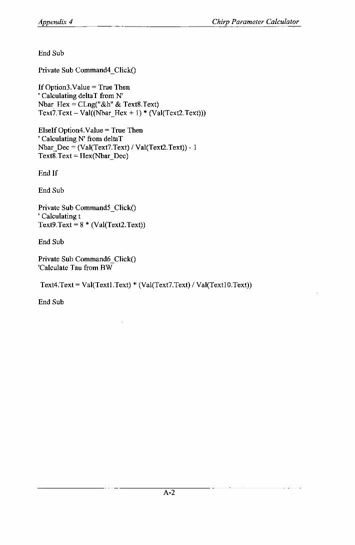
Appendix 4
End Sub
Private Sub Command4 _Click()
If Option3. Value = True Then 'Calculating deltaT from N' Nbar_Hex = CLng("&h" & Text8.Text) Text7.Text = Val((Nbar_Hex + 1) * (Val(Text2.Text)))
Elseif0ption4.Value =True Then 'Calculating N' from deltaT Nbar_Dec = (Val(Text7.Text) I Val(Text2.Text))- 1 Text8.Text = Hex(Nbar_Dec)
End If
End Sub
Private Sub Command5 _Click() ' Calculating t Text9.Text = 8 * (Val(Text2.Text))
End Sub
Private Sub Command6 _Click() 'Calculate Tau from BW
Chirp Parameter Calculator
Text4.Text = Val(Textl.Text) * (Val(Text7.Text) I Val(TextlO.Text))
End Sub
A-2

Appendix-5 Publications and Outputs
Appendix- 5 Publications and Outputs
A5.1 Conference Publication
The following is an abstract submitted to commission C of the National USRI
Symposium in Portsmouth, 2"d-3rd July 2007.
A-1

Appendix-5 Publications and Outputs
Imaging with 1 GHz Harmonic Radar Prof. Sana Salous [email protected]
S. M. Farrukh Aslam [email protected]
A 'Harmonic Radar' is a device that illuminates a region of space with RF waves and receives the harmonics of the transmitted frequencies. The received data can then be processed to find the exact location and mobility of the points causing the generation of these harmonics. It works on the principle of radar transmitting a chirp signal and receiving harmonics of the transmitting frequency. Work is currently being carried out at the 'Centre for Communication Systems' in Durham University funded by HMGCC on the design and implementation of a novel Wideband Harmonic Radar system with a suitable waveform and multiple antenna arrays with algorithms for angular information.
Radio sites consist naturally of metallic structures. Metals are always covered by an oxide film due to the metal reacting chemically with the oxygen in air. The rate of this oxide formation depends largely on the environment. Any oxide film between metallic contacts will cause non-linearity. RF currents passing through these junctions would generate harmonics. When RF signals at two frequencies fl and f2 pass through a non-linearity they create signals at their sum and difference frequencies. These are known as 'inter-modulation products'. This generation of inter-modulation products when radio waves interact with rusty parts is called as the 'Rusty Bolt Effect'. Radio spectrum is carefully controlled for optimal usage of the available frequencies so that different services operate in well-defined frequency channels. Ofcom has set some standards for radio site engineering. This set of standards is given in the document 'MPT 1331: Code of Practice for Radio Site Engineering'[!]. Any transmission site which is not following these codes would likely cause interference to other users. It is important that radio engineers should check the sites for their compliance with these codes. If a particular radio site is causing interference due to the rusty-bolt effect, the corroded points must be located to minimize their effect using the Harmonic Radar.
This Harmonic Radar will transmit at lGHz and receive at 2/3 GHz rh, ... ~-1 -.C:-~• --- --L - r '
1 _____ -.aa.ao valTleO OUt is
on the chirp generator which is the heart of the transmitter. It consists of a Direct Digital Frequency Synthesizer (DDFS), mixers, Programmable Phase Locked Loops (PLLs), Band Pass Filters, power amplifier and a digital controller. DDFS AD9854 has been used in the chirp generator. Future work will focus on the remaining part of the transmitter and the receiver, primarily on the antenna arrays and the accompanied signal processing.
Reference:
1. MPT 1331: Code of Practice for Radio Site Engineering
A-2

Appendix-5 Publications and Outputs
A5.2 Other Outputs
Following is a poster presented at the Annual School Research Day, University of Durham, June 2007
•• ~rDurham Unin~rsit}'
Electronics School of
Engineering
Centre for Communication Systems r---------------------------~ Experimental Investigation Into the feasibility of MIMO techniques In HF Band By Dr. w. 1. Kassem
•'!'SI pr~.u:s ~~.A:i';t~ la:wH!'I ~fh(I"-..L~ntt', I:M !itltMU (Fr~J ~OH.
• i.'tt MLVC {M;i.";'P<t ir~.P. Mai'f>ft Ol.ftpl./t) ~~,jf- us•• art~ MnJ)'t .r.l:mh the \"~~r.aM~•r~r1oi-.'Wt.Wt'tt~I"Mf~adty • Tbf ~.ant"''<ft:.ff .aM+,* r•:ltJV+r wil bl t-Wtln ~M mNMOihMr.b will- b+ Uil.trt .a.M
¥.3lySN 14 ~ .. stiQatt m. potwWl.a~~ir1 oftN V.lUO ~~~to eo:;om~.aioo :11 tr,. f'lF b.t"d
lmaging With 1 GHz Hru:monle Detector By M. F. ASiam
.Pro;t« b~ l~td b1 t-!MCCC tHw~l{(s ~'trnmft'!t~"'"~li.MCtrtftj
·~ ~nd imo-!•~·n'"~ti<xl «.a nwtl Wab~r~d "'''l't!Ot!k R:>l:btw:\h a --..~tU~• w..,.fem!
Collaborations:
A-3
spectrum Oeeupaney Analysis for Cognitive Radio ByZheWang
·~~mayl>t .a~-ltttnSM i1'X1"'!W:!~~~t.i'4 r~
a.fti~~.t.UM-I':Nil~al:lk~tU!'rl
Simulator of Radio Systems By Odlrl C. Oghre
.0.~ fOf Oi*.a6on ""l~• with lt-t E£E tro, '' stand.uds ~t WirfiMt B~d .A4t:Ms
l!(j, ••• :&l. •EIHI'Qt iJ to~~. to tt!illUt• h BEA fo -~· '"' ~smihklf",sl'll$\4 ~~
Universite de Rennes

Appendix-5 Publications and Outputs
Following is a poster accepted to be presented at the GRADUK Northeast 2008 Poster Competition being held at University of York, ih March 2008.
~· ~,.Durharn
Wideband Harmonic Radar Detection Can we detect very small bugs ?
University Prof. Sana Salous, Or S.M. Feeney, Farrukh Aslam
Department of Eng;neenng, Durham University s.m.farrukh-asBmC):iur.ac.uk
Radio sites consist naturally of metallic structures. Aryt oxide film between metallic contacts will cause non-linearity. Currents passing through these junctions would generate harmonics. This generation of inter-modulation products when radio waves interact with rusty parts is called as the 'Rusty Bolt Effect'. These rusty boHs cause the transmission sites to operate beyond well-<lefined frequency bands. Ofcom has set some standards for radio s~e engineering which should be abided by all transmission s~es . 1
2. ObJecttves
To develop a Radar system
that would accurately detect
the 'rusty bolt' joints (bugs)
causing the harmonic
E.,....!.ltflrllwfltOtiWalio•ht•tMI411runufl
ll~;:~
> Chi rp type Transrn~ Signal at 960 MHz • 1920 MHz
>Antenna Arrays: 'N' Transmitter and 'M' Receiver
> Signal Processing Algorithms ! to find the direction of a rrivat of th~ receiving waves (e.g. SAGE A!:;&r~m)
\,,
A-4
,......---~-....--
Origin .. Chirp Sl_gnaJ
(45 • 120MHzl
Unfiltered Signal
~...
Clean Upconv•rtN Signal
(240 MH:r. - 315 MHz)
Accuracy and resolution of this harmonic radar depends upon the bandwidth and type of the transm~ signal. The frequency synthesizer board produces a clean chirp signal at 45- 120 MHz. tt is then successfully up converted and then filtered to produce a signal at 240 - 315 MHZ. The resutting frequency response graphs on a spectrum analyser are shown. lt would then be up converted to a 1GHz transm~ signal.
Further work needs to be done to complete the receiver part of the project. Signal Processing Algorithms would then be developed that would use an appropriate number of receiving antennas to collect data and then process them to retrieve useful Information.
6. Reference 1. MPT 1331 : Code of Practice for Radio Site Engineering