dual mode logic design for energy efficiency and high
TRANSCRIPT

Received April 21, 2013, accepted May 2, 2013, date of publication May 15, 2013, date of current version May 21, 2013.
Digital Object Identifier 10.1109/ACCESS.2013.2262015
Dual Mode Logic—Design for Energy Efficiencyand High PerformanceITAMAR LEVI (Student Member, IEEE)1 AND ALEXANDER FISH (Member, IEEE)21Electrical and Computer Engineering Department, Ben-Gurion University, Beer-Sheva 84105, Israel2Faculty of Engineering, Bar-Ilan University, Ramat-Gan 52900, Israel
Corresponding author: I. Levi ([email protected])
ABSTRACT The recently proposed dual mode logic (DML) gates family enables a very high level of energy-delay optimization flexibility at the gate level. In this paper, this flexibility is utilized to improve energyefficiency and performance of combinatorial circuits by manipulating their critical and noncritical paths. Anapproach that locates the design’s critical paths and operates these paths in the boosted performance modeis proposed. The noncritical paths are operated in the low energy DML mode, which does not affect theperformance of the design, but allows significant energy consumption reduction. The proposed approach isanalyzed on a 128 bit carry skip adder. Simulations, carried out in a standard 40 nm digital CMOS processwith VDD = 400 mV, show that the proposed approach allows performance improvement of X2 alongwith reduction of energy consumption of X2.5, as compared with a standard CMOS implementation. AtVDD = 1.1 V, improvements of 1.3X and 1.5X in performance and energy are achieved, respectively.
INDEX TERMS Dual Mode Logic, energy efficiency, high performance, critical paths, energy-delayoptimization.
I. INTRODUCTIONThe DML logic gates family was proposed in order to pro-vide a very high level of energy-delay (E-D) optimizationflexibility [1]–[3]. DML allows an on-the-fly change betweentwo operational modes at the gate level: static mode anddynamic mode. In the static mode, DML gates consume verylow energy, with some performance degradation, as comparedto standard CMOS gates. Alternatively, dynamic DML gatesoperation obtains very high performance at the expense ofincreased energy dissipation. A DML basic gate is based on astatic logic family gate, e.g., a conventional CMOS gate, andan additional transistor. While DML gates have very simpleand intuitive structure, they require an unconventional sizingscheme to achieve the desired behavior [1], [3].
Performance of most digital circuits and systems is deter-mined by the delay of critical paths (CP). Even though stan-dard synthesis tools attempt to design logic blocks withoutCP [4]–[6] (i.e. equalized path delay), the slack from thetargeted Clk (Clock) frequency always exists and should berepaired by designers. Many methods have been proposedto address these slacks . These methods include adaptivevoltage scaling with a CP emulator circuit [7], multi oxidethickness driven threshold-voltages, multi-channel lengthsfor energy reduction in the non-CPs and performance boostin the CPs [8], [9]. Meijer et al. and Liu et al. applied a
body bias on a non-CP to improve energy consumption andincrease performance of the CPs, respectively [10], [11] .While the aforementioned methods solve the critical pathslack problem, in most cases they also result in a significantincrease of energy consumption. In addition to these gate levelapproaches higher-level approaches were presented such asmulti-mode logics, parameterised logic [24]. In this paper, weissue both the gate and higher archeitectural levels.This paper proposes to meet the delay requirements of
CPs along with lowering the over-all energy consumptionof the design by utilizing the powerful modularity of DML.We propose and analyze a new approach, which locates thedesign’s CPs and utilizes the on-the-fly modularity of DMLto operate these paths in the boosted (dynamic) performancemode. The non-critical paths are operated in the low energystatic DML mode, which does not affect the performance ofthe design. Since in most cases the majority of gates in thedesign are not on the CPs, the increase in energy consumptionof the critical paths will be negligible in comparison to thegeneral circuit consumption. Moreover, DML static gatesdissipate less power than their CMOS counterparts, resultingin reduced power dissipation of the whole design.The proposed approaches have been analyzed on a 128bit
Carry Skip Adder (CSA) benchmark. Simulations, carried outin a standard 40nm CMOS process with VDD = 400 mV,
258 2169-3536/$31.00 2013 IEEE VOLUME 1, 2013
I. Levi, A. Fish: DML—Design for Energy Efficiency and High Performance
show that the proposed approaches allow performanceimprovement of X2 along with reduction of energy consump-tion of X2.5, as compared to a standard CMOS implemen-tation. At VDD = 1.1V, improvements of 1.3X and 1.5X inperformance and energy were achieved, respectively.
The rest of this paper is constructed as follows: Section IIdiscusses basic properties of the DML family. The proposedCP-DML approach is discussed in Section III. Section IVpresents the test-bench, chosen for the evaluation of the pro-posed approach. Simulation results of the benchmark cir-cuits are presented in Section V. Section VI concludes thepaper.
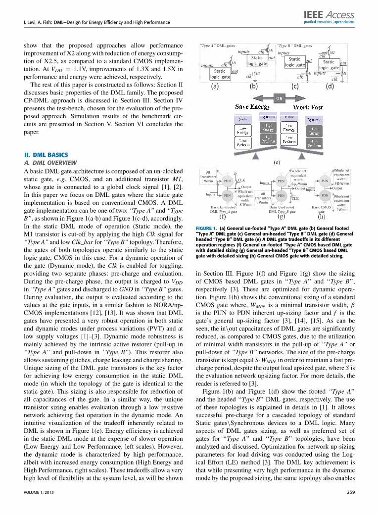
II. DML BASICSA. DML OVERVIEWA basic DML gate architecture is composed of an un-clockedstatic gate, e.g. CMOS, and an additional transistor M1,whose gate is connected to a global clock signal [1], [2].In this paper we focus on DML gates where the static gateimplementation is based on conventional CMOS. A DMLgate implementation can be one of two: ‘‘Type A’’ and ‘‘TypeB’’, as shown in Figure 1(a-b) and Figure 1(c-d), accordingly.In the static DML mode of operation (Static mode), theM1 transistor is cut-off by applying the high Clk signal for‘‘Type A’’ and low Clk_bar for ‘‘Type B’’ topology. Therefore,the gates of both topologies operate similarly to the staticlogic gate, CMOS in this case. For a dynamic operation ofthe gate (Dynamic mode), the Clk is enabled for toggling,providing two separate phases: pre-charge and evaluation.During the pre-charge phase, the output is charged to VDDin ‘‘Type A’’ gates and discharged to GND in ‘‘Type B’’ gates.During evaluation, the output is evaluated according to thevalues at the gate inputs, in a similar fashion to NORA/np-CMOS implementations [12], [13]. It was shown that DMLgates have presented a very robust operation in both staticand dynamic modes under process variations (PVT) and atlow supply voltages [1]–[3]. Dynamic mode robustness ismainly achieved by the intrinsic active restorer (pull-up in‘‘Type A’’ and pull-down in ‘‘Type B’’). This restorer alsoallows sustaining glitches, charge leakage and charge sharing.Unique sizing of the DML gate transistors is the key factorfor achieving low energy consumption in the static DMLmode (in which the topology of the gate is identical to thestatic gate). This sizing is also responsible for reduction ofall capacitances of the gate. In a similar way, the uniquetransistor sizing enables evaluation through a low resistivenetwork achieving fast operation in the dynamic mode. Anintuitive visualization of the tradeoff inherently related toDML is shown in Figure 1(e). Energy efficiency is achievedin the static DML mode at the expense of slower operation(Low Energy and Low Performance, left scales). However,the dynamic mode is characterized by high performance,albeit with increased energy consumption (High Energy andHigh Performance, right scales). These tradeoffs allow a veryhigh level of flexibility at the system level, as will be shown
Static
logic gate
inputs clk
out
M1Static
logic gate
inputs
clk
out
M1
(a) (c)
Static
logic gate
inputs clk
out
M1
Static
logic gateinputs
clk
out
M1
(b) (d)
clk
clk
M2
M2
“Type B” DML gates“Type A” DML gates
PUN
PDN
Inputs Output
Whole net
equivalent
width:
f·β·Wmin
Whole net
equivalent
width:
f·WminBasic CMOS
gate
PUN
PDNInputs
Output
All
Transistors
: Wmin
Whole net
equivalent
width:
S∙WminBasic Un-Footed
DML Type_A gate
VDD
CLK PUN
PDN
Inputs
Output
All
Transistors
: Wmin
Whole net
equivalent
width:
S∙μr∙Wmin
Basic Un-Footed
DML Type_B gate
CLK
(h)(g)(f)
FIGURE 1. (a) General un-footed ‘‘Type A’’ DML gate (b) General footed‘‘Type A’’ DML gate (c) General un-headed ‘‘Type B’’ DML gate (d) Generalheaded ‘‘Type B’’ DML gate (e) A DML gate tradeoffs in its differentoperation regimes (f) General un-footed ‘‘Type A’’ CMOS based DML gatewith detailed sizing (g) General un-headed ‘‘Type B’’ CMOS based DMLgate with detailed sizing (h) General CMOS gate with detailed sizing.
in Section III. Figure 1(f) and Figure 1(g) show the sizingof CMOS based DML gates in ‘‘Type A’’ and ‘‘Type B’’,respectively [3]. These are optimized for dynamic opera-tion. Figure 1(h) shows the conventional sizing of a standardCMOS gate where, WMIN is a minimal transistor width, βis the PUN to PDN inherent up-sizing factor and f is thegate’s general up-sizing factor [3], [14], [15]. As can beseen, the in\out capacitances of DML gates are significantlyreduced, as compared to CMOS gates, due to the utilizationof minimal width transistors in the pull-up of ‘‘Type A’’ orpull-down of ‘‘Type B’’ networks. The size of the pre-chargetransistor is kept equal S ·WMIN in order to maintain a fast pre-charge period, despite the output load upsized gate, where S isthe evaluation network upsizing factor. For more details, thereader is referred to [3].
Figure 1(b) and Figure 1(d) show the footed ‘‘Type A’’and the headed ‘‘Type B’’ DML gates, respectively. The useof these topologies is explained in details in [1]. It allowssuccessful pre-charge for a cascaded topology of standardStatic gates\Synchronous devices to a DML logic. Manyaspects of DML gates sizing, as well as preferred set ofgates for ‘‘Type A’’ and ‘‘Type B’’ topologies, have beenanalyzed and discussed. Optimization for network up-sizingparameters for load driving was conducted using the Log-ical Effort (LE) method [3]. The DML key achievement isthat while presenting very high performance in the dynamicmode by the proposed sizing, the same topology also enables
VOLUME 1, 2013 259

I. Levi, A. Fish: DML—Design for Energy Efficiency and High Performance
improved energy efficiency in static mode, as compared to aconventional CMOS.
B. STATIC DML AS A SEMI-ENERGY-OPTIMAL CMOSDesign space of a CMOS gate is mainly influenced by VTH ,transistor width, VDD, channel length, oxide thickness andbody voltage. The influence of those parameters on E-Dplain-optimization is being explored. For the CMOS family,the symmetry of the gate (i.e. equal rise and fall times) ishighly important. This is due to the fact that in a combina-tional system there is always some uncertainty regarding thetransition type. As a result, the pull-up network (PUN) ofCMOS gates, which is constructed by low mobility PMOSdevices, is sized up by the β parameter [14].When optimizinga CMOS gate’s energy at the expense of its performance,the transistor’s width is the main parameter used for reduc-ing the energy consumption. This is due to several facts:(1) Switching energy is proportionate to the load andquadratic dependent on VDD. Under energy optimization, thesymmetry of the gates’ performance does not constitute a con-straint so the transistor’s width can be reduced, as well as β.This significantly lowers the load capacitances. (2) With cir-cuit’s VDD lowering [26], [27] and technology scaling, leak-age energy has become one of the key factors for static powerdissipation. The leakage energy is caused by the numerousleakage currents of a device. The main leakage currents arethe sub-threshold and gate leakage currents [16], [27]. Thesecurrents are linearly dependent on the transistor’s width Andunder energy optimization they are considerably reduced.
CMOS based DML operated in static mode with transistorsizes optimized for the dynamic mode is de facto a semi-energy-optimal CMOS structure with an additional negligibleoutput capacitance for the Clk transistors (transistors M1 andM2). Static DML is still highly robust due to its complemen-tary nature [1], [2] and withstands aggressive voltage scaling.This methodology can also be referred to as a stand-alonetechnique for reducing the energy consumption of digital cir-cuits. The E-D tradeoff space under this approach is very wideand in this paper the discussion is limited only to transistorssizing, as shown in Figure 1(f) and Figure 1(g) for DMLgates.
III. CP-DML APPROACHES FOR ENERGY EFFICIENCYAND HIGH PERFORMANCEThis section elaborates the proposed design approaches forenergy efficient and high performance design of combina-torial systems. Sub-Section A presents an approach whichutilizes DML gates in the dynamic mode on the CPs in orderto improve their delays. Sub-Section B elaborates variousaspects of energy reduction of all non-CP portions of thedesign.
Theoretically, a general DML design can be controlled(input signal-driven control or external signal-driven con-trol) to operate each gate in one of two modes: Static andDynamic. This means that a general design can be operatedin 2(Gates Number) different options, each one leading to a
FIGURE 2. (a) DML design optional operation modes (b) DML designdegenerated to the dynamic mode (c) DML design degenerated to thestatic mode (d) DML design where only the CP’s are dynamically operatedwhile the rest of the design operate in the low energy static mode. Where,Dyn. And Stat. stands for Dynamic and Static respectively.
different operating point on the E-D space of the design.Figure 2(a) visualizes this modularity. The degeneratedapproaches for operating all the gates in one of the twomodes, similar to a sole gate, are shown in Figures 2(b)and 2(c). Switching between these two modes leads to thedistinct tradeoff, meaning that the design is optimized eitherto achieve maximum performance or minimum energy con-sumption.
A. SOLVING CPs TIMING VIOLATIONSAs discussed in Section I, the CPs of a design are automati-cally identified using standard design flow tools. By replacingonly these paths with DML gates and applying the dynamicmode on these paths, their delay can be reduced. The rest ofthe design is implemented using standard CMOS static logic.Of course, special design constraints should be enforced inall the intersections between a static path and a dynamic one.In some of these cases, a footer\header should be applied[1], [2], [17]. Figure 2(d) presents a design in which theCPs were located and only those paths were given the optionto toggle between dynamic and static mode, according tothe system requirements. If the system design can withstandslower operation, the CP logic will operate in static mode.If the system is required to meet the defined Clk period forall cycles, the CPs will operate in the dynamic mode. Suchapplication can be a smart phone that operates with twofrequencies: slow one for power save/ hibernating mode anda fast one for video streaming. To emphasize, low complexitysystems will normally bear only one frequency for operationand therefore the CPs will constantly operate in the dynamicmode. Normally, the amount of gates on the CP is small ascompared to the total amount of gates in the design. There-fore, in most cases, the inherent dynamic-operation energyof these CPs will lead to a non-significant increase in totalenergy consumption of the design.
260 VOLUME 1, 2013

I. Levi, A. Fish: DML—Design for Energy Efficiency and High Performance
B. SOLVING THE CPs TIMING VIOLATION WHILEREDUCING THE TOTAL ENERGY CONSUMPTIONAs described in the previous Sub-Section, the CPs aremappedand operated in the dynamic DML mode. In Sub-Section A,the rest of the circuit was assumed to keep a standard CMOSlogic gates topology. Therefore, the design was proposed tosolve the CPs’ timing constraints at the expense of a smalldegradation in energy consumption, as compared to a com-plete CMOS design. In this Sub-Section, all portions of thedesign, which are not a part of the CPs, will be mapped tostatic mode DML gates (similar to semi-energy optimizedCMOS gates, described in section II). In most designs, thesenon-CPs are not time constrained and therefore the asym-metry behavior of their transitions and consequently theirperformance degradation will withstand the Clk period. Theuse of the static DML mode for the mass majority of gatesin the design will lead to a significant reduction in the totaldynamic and static energy consumption. Figure 3 visualizesthis approach.
IV. MODULAR BENCHMARKThis section, presents the chosen benchmarks. As depicted inSection III we will discuss three designs:
1) A CPs accelerator, as described in Sub-Section III(A),which has 2 operation modes:
– ‘‘DML Carry Path-Dynamic’’- The DML CPs areactivated in the dynamic mode.
– ‘‘DMLCarry Path-Static’’- The DMLCPs are acti-vated in the static mode.
In both of these modes the rest of the non-CPs portionsof the system are designed with standard CMOS.
2) A CPs accelerator with low energy consuming non-CPs, as described in Sub-Section III(B), which has 2operation modes:
– ‘‘DMLCarry Path-Dynamic.With low energy non-CPs-Static’’ - The DML CPs are activated in the
FIGURE 3. A mapped circuit for CP’s and non-CP’s while the formeroperate in the dynamic mode and the latter in the static mode.
dynamic mode, while the rest of the system oper-ates in the DML static mode.
– ‘‘DML Carry Path- Static. With low energy non-CPs- Static’’ - The DML CPs are activated in theDML static mode, similar to the rest of the system.
3) CMOS equivalent design.
A Carry Skip Adder (CSA, also called carry bypass adder),was chosen as a benchmark to demonstrate and evaluate theproposed concept. The CP of the CSA increases as a functionof the number of inputs, making it possible to examine theE-D trends as a function of the CPs lengths. It is impor-tant to note that the proposed methods can apply over anycombinatorial circuits and a CSA was chosen only due to itsmodularity and simplicity.
A. CMOS CSA DESIGNA conventional CSA is composed of a set of Ripple CarryAdder (RCA) blocks. They essentially utilize the carry prop-
FIGURE 4. Test-bench circuit: CMOS designed CSA where the non-elementary CMOS gates such as the mirror FA and MUX are presented withtransistor sizes. Transistor sizes are marked with X’Number’ Where, X represents the multiplication in Wmin (technology minimum transistor width).
VOLUME 1, 2013 261

I. Levi, A. Fish: DML—Design for Energy Efficiency and High Performance
agation in order to skip the carry from one RCA to the nextRCA block. It is possible to predict the propagation of thecarry by a simple XOR gate [18]. Such prediction mechanismcan substantially reduce the delay [19]. The CP in CSA occurswhen the carry ripples at the first block, and then skips therest of the blocks and then ripples again at the last block.This is the longest possible route in the CSA. Lehman et al.have researched CSAs with non-uniform sized distributedRCA blocks [20]. Majerski has presented a multi-level ofcarry-skip propagation architecture [21]. Guyot et al. andOklobdzija et al. proposed algorithms for choosing optimizedblock sizes [22], [23]. In this paper, a simple CMOS CSAdesign with a fixed size of 4-bits blocks was designed, asshown in Figure 4. Clearly, the methods presented in thispaper can be generalized to any CSA block size constant orvariable and for multi or single level carry path. A generalsingle-bit Full Adder (FA) equations are:
S = A⊕ B⊕ Cin (1)
Cout = AB+ Cin · (A+ B) (2)
P = A⊕ B (3)
Where, ⊕ is the conventional XOR symbol. For an RCA,Cout will be an input to the next FA. For the CP, the carrywould propagate through all FAs. Due to the fact that Coutis on the CP for each RCA, the mirror circuit for computingCout is used [19], as shown in Figure 5. This circuit calculatesthe inverted value Cout and when serially chained, it reducesthe circuitry on the CP (i.e. eliminates one inverter for eachFA). Furthermore, the use of the mirror adders creates theneed for inverting inputs for all odd FAs and inverting outputsfor all even FAs [18], as shown in Figure 4. All the logicalgates presented in the figure are constructed with standardCMOS.A standard sizing optimization, for the RCAofmirrorFAs using Logical Effort [15], yields the sizing factor Fi(as shown in Figure 4 for all the carry path gates). For alli’s which are a multiple of 4, Fi = 1 and for all the restFi = 3.5.
B. DML CRITICAL PATH DESIGNFigure 5 shows the DML implementation of the CSA’s CP.The CP flows through the first NOR (assuming that the carryin of the whole design is 0) and through all the MUXs of thedesign. The gate level implementation of the CP can be con-structed with various topologies of DML: DML NOR gatesare most efficiently implemented in the ‘‘Type A’’ topologiesand NAND gates in ‘‘Type B’’, as discussed in [1]–[2]. TheBoolean logic does not allow an efficient implementation ofa MUX with a NOR following a NAND or vice-versa, whichis the preferred topology for DML logic design.
Therefore, in the chosen topology, the CP is composed onlyof NANDs (where one of them is implemented using efficient‘‘Type B’’ and the other one has a less optimal ‘‘Type A’’ struc-ture). The last inverter in each RCA block is a headed ‘‘TypeB’’ inverter, which maintains correct Pre-Charge phase for theCP. The sizes of the transistors in terms of minimal transistor
FIGURE 5. DML Critical Path design for the selected CSA. The figure showstransistor width for gates of interest.
width are shown in Figure 5. In the design, implemented insuch way, only 8% of transistors will (optionally) operatedynamically, while the remaining 92% of the transistors arekept at the low energy static mode. This modular design keepsthe same complexity and the same dynamic-to-static-gates-ratio, as a function of the input vector’s length, N [bits].
V. SIMULATION RESULTSThe modular benchmarks circuits, described in the previoussection were simulated in a standard 40nm CMOS process,using the Spectre Cadence simulator [25]. Implementationsof these methods on the benchmark CSAs were mainly exam-ined over the E-D plain and as a function of the operatingvoltage and the CP’s length. Note, the naming convention forthe different designs and operating modes is elaborated in thepreface of Section III. All energy and delay measurements areper-operation.
A. THE E-D PLAIN AS f (VDD)Each design was carefully measured as a function of the sup-ply voltage. Now-days, even standard manufacturers realizethe potential held in the near\sub-threshold operation. Stan-dard cell libraries, designed for 700-800 mV, are widespread.For special low power applications, the libraries are normallydesigned for 200-500 mV. In order to examine the proposedconcept both for low voltage [26] and strong inversion oper-ations, measurements are performed with supply voltagesvarying from 0.4V to 1.1V.The E-D curves for all designs of a 128 bit CSA are plotted
in Figure 6(a). The curves’ order from top to bottom is:(1) CMOS, (2) CMOS design with a CP in Dynamic DMLmode, (3) CMOS design with a CP in static DML mode,(4) low energy non-CP design with a CP in Dynamic DMLmode, and (5) Low energy non-CP design with a CP in staticDML mode. The last two curves are presented in the grayenhanced region, at the bottom of the graph. This region
262 VOLUME 1, 2013

I. Levi, A. Fish: DML—Design for Energy Efficiency and High Performance
0.9V
1V
1.1V
1.1V
0.9V
1V
1.1V
1V
1.1V
4.0E-13
5.0E-13
6.0E-13
7.0E-13
8.0E-13
9.0E-13
1.0E-12
1.1E-12
1.2E-12
1.0E-09 1.5E-09 2.0E-09 2.5E-09 3.0E-09En
erg
y/W
ors
t C
ase
Op
erat
ion
[J]
Delay/Worst Case Operation [Sec]
E-D Plain for a 128 Bit CSA implamanted in CMOS and
DML as a function of VDD (1) CMOS
(2) DML Carry
Path- Dynamic
(3) DML Carry
Path- Static
(4) DML Carry
Path- Dynamic.
With Low Energy
non-CPs- Static(5) DML Carry
Path- Static. With
Low Energy non-
CPs- Static
~X1 in
Energy
~X1.2 Performance
Improvement
~X1.5
Energy
Improvement
~X1.4 Performance Degradation
Low Energy CMOS/ Static
mode DML region
FIGURE 6. E-D measurements for all 128 bit designs (a) E-log(D) plots forall supply voltage from 0.4V to 1.1V (b) Enlarged E-D plots for 0.4-0.5Vsupply voltages (c) Enlarged E-D plots for 1-1.1V supply voltages.
represents the low energy area of the E-D plain, achievedby implementing all non-CPs with the low energy DMLstatic mode (which, as described in Section II, could be alsoreferred as ‘‘low energy CMOS’’). The two areas of interestare circled at the edges of Figure 6(a) and are enlarged inFigures 6(b) and 6(c). Figure 6(b) shows the tradeoff area
for a 400 mV operating voltage for all designs. Figure 6(c)presents that same tradeoff for 1.1V. These two extremi-ties clearly show that these designs are highly flexible inenergy consumption and performance, for the whole range ofvoltages.The conclusion from analyzing the DML enhanced CP
plots (second and third curves) compared to the CMOS plot(first curve) for the 0.4V supply (Figure 6(b)) is that the DMLenhanced CP achieves X2 in performance. This achieve-ment, however, comes at the expense of a 16% increase inenergy consumption. If the system is such that two opera-tional frequencies are allowed, when a low-power operationis required, the static mode (with a low frequency) could beapplied yielding X2.5 energy improvement at the expenseof performance degradation of X1.3. This ability to changeoperating conditions on the E-D plain on-the-fly is a featurethat can be easily utilized to improve the system flexibilityand E-D efficiency.For the 1.1 V supply (Figure 6(c)), it is shown that boosting
the performance of the CP by 20% increases energy consump-tion by only 3%. Again, if the system is such that two oper-ational frequencies are allowed, when a low-power operationis required, the static mode could be applied yielding X1.5energy improvement at the expense of performance degrada-tion of X1.4. These results reveal that a low-voltage operationmagnifies the differences between the different modes. Thereare a few reasons for this trend. First, the performance advan-tage of DML circuits in the dynamic mode over standardCMOS intensifies with the supply voltage lowering [1]–[2],[26], [27]. The second, less dominant factor is the reducedsensitivity of DML circuits to increased leakage currents atlow supply voltages [1]–[2].By examining the DML performance optimized CP with
low energy non-CP plots (two lowermost curves), it is clearthat the total energy is reduced by X2-X3 (gray region)for all voltage regions - which is substantial. In addition,the improvement in CP performance of X1.3 and X2.1 areachieved for the 1.1V and 400 mV supplies, accordingly. Theresults for the CP are quite similar to the results achievedfor operating without the low energy non-CP gates. This isdue to the fact that the CPs themselves have not changed. Toconclude, the flexibility of theDMLdesign led to a significantimprovement in both energy and performance.
B. THE E-D PLAIN AS f(N)This Sub-Section examines the efficiency of the proposedconcept as a function of the CP’s length, which is closelyrelated to the size of the design. The CSA’s size/lengthdepends on the number of inputs, N . Figure 8 shows the E/Dtrends for all designs as a function of N . Each plot startswith the minimal CP related to N = 4 and goes up to thelongest examined CP of N = 128. The point where N = 128appears both in Figure 6 and Figure 7. The key point of thisanalysis is to show the scalability of the method for variousdesign sizes and not only for a very long CP. The E-D trendsof different designs with N = 128 were discussed in Sub-
VOLUME 1, 2013 263

I. Levi, A. Fish: DML—Design for Energy Efficiency and High Performance
4 Bit
64 Bit
128 Bit
4 Bit
16 Bit
32 Bit
64 Bit
128 Bit
16 Bit
32 Bit
64 Bit
128 Bit
32 Bit
64 Bit
128 Bit
0.0E+00
4.0E-14
8.0E-14
1.2E-13
1.6E-13
0.E+00 2.E-07 4.E-07 6.E-07 8.E-07 1.E-06
En
erg
y/W
ors
t C
ase
Op
erat
ion [
J]
Delay/Worst CaseOperation [Sec]
E-D Plain for CSA implamanted in CMOS and DML as f(N)
for VDD=400 mV (1) CMOS
(2) DML Carry Path-
Dynamic
(3) DML Carry Path-
Static
(4) DML Carry Path-
Dynamic. With Low
Energy Non-CPs- Static
(5) DML Carry Path-
Static. With Low
Energy Non-CPs- Static
~X2 Performance Improvement
~X1.33 Performance
Degredation
~X1.15
Energy
Degradation
~X2.5 Energy
Improvement
4 Bit
64 Bit
128 Bit
4 Bit
16 Bit
32 Bit
64 Bit
128 Bit
64 Bit
128 Bit
32 Bit
64 Bit
128 Bit
9.0E-14
4.9E-13
8.9E-13
1.3E-12
0.E+00 5.E-10 1.E-09 2.E-09 2.E-09 3.E-09 3.E-09
En
erg
y/W
ors
t C
ase
Oper
atio
n [
J]
Delay/Worst CaseOperation [Sec]
E-D Plain for CSA implemanted in CMOS and DML as f(N),
VDD=1.1V (1) CMOS
(2) DML Carry Path-
Dynamic
(3) DML Carry Path-
Static
(4) DML Carry Path-
Dynamic. With Low
Energy Non-CPs-
Static(5) DML Carry Path-
Static. With Low
Energy Non-CPs-
Static
~X1.2 Performance
Improvement
~X1.4 Performance
Degredation
~X1.5 Energy
Improvement
~X1 in Energy
FIGURE 7. E-D measurements as a function of the CSA size (a) For 0.4V(b) For 1.1 V.
Section A and therefore will not be discussed here again.Figure 7(a) and Figure 7(b) show that as N increases (orlog2(N ) increases), the scalability of the energy and perfor-mance improvement is almost constant both for 400mV and1.1V. There is another interesting point regarding the 128bit design with VDD = 1.1V, presented in Figure 7(b): theLow Energy design (DML static mode for non-CPs) withCPs operated in the dynamic mode, consumes slightly moreenergy than the standard CMOS non-CP design with DMLdynamic CP, but achieves more than X2 improvement inperformance.
As can be seen from Figure 7(a), all designs (N = 4..128)with performance improved CP show a significant improve-ment in performance at 400mV, as compared to the CMOScounterparts. However, for the 1.1V supply (Figure 7(b)),this efficiency can be observed only from N = 32. Thisbehavior naturally depends on the specific gates topology ofthe chain, as mentioned in Section IV B. The CSA specificdesign represents an average case where some of the DMLgates on the CP are very fast in comparison to CMOS, such as‘‘Type B’’ NAND, and others hold very small improvements,such as ‘‘Type A’’ NAND. For this reason, we can expect that
for other benchmarks, the improvement in E/D will occur foran N > NMIN .
C. STIMULI INPUT VECTOR COMPLEXITYThe measurements presented in the previous two Sub-Sections simulated input stimulus that activated the CP ofeach circuit. These stimuli trigger the worst delays whichare possible for these designs. Each circuit requires differentinput for activating its CP. The worst case of energy consump-tion depends on the input vector. Worst case is reached whenthe input vector switches as many gates as possible for eachRCA chain (static portions of the design). In the previous twoSub-Sections, for the case of 128 bit CSA, input vectors werechosen to switch 40 outputs, regardless the CP switching.This approach is quite pessimistic, since the average numberof switching outputs is lower than 40. Let’s assume equalprobabilities for logic ‘‘1’’ and logic ‘‘0’’ for each input. Theprobability for a carry in a FA is q = 0.5. The probability fora carry to propagate through K successive bits is:
qk =12·12·12· · ·
12︸ ︷︷ ︸
K
=12k
(4)
Alternatively, the probability of a carry being either killedor generated through K successive bits is 1-qk . Therefore,the probability for propagating more than 4 bits is 6.25%,which is quite low. For example, let’s consider the 128 bitdesign composed of 4 bit RCAs (i.e. 32 segments): ripplingof 2 bits inside each 4 bit RCA (in addition to the switching ofthe whole CP) is, in terms of probability, a quite reasonableor even a harsh case. Nevertheless, input vectors which aremore energy consuming (for the static parts of the design)were simulated (60 and 80 switched outputs). The anticipatedresults showed that as the input stimulus complexity rises,the additional energy required for the dynamic operated CPbecomes more and more negligible in comparison to thetotal energy of the designs. These results are, of course,reassuring for all worst\typical\best case input vectors,energy-wise.
VI. CONCLUSIONCP timing violation and energy minimization are importantissues in all digital circuits. The invaluable possibilities,inherent to design with DML gates, leverage the flexibilityof the design to meet CP timing along with reducing thetotal energy consumed by the circuit, as shown in this paper.Until now, meeting the CP timing was closely related to arise in the consumed energy by conventional methods. In thiswork this paradigm is contradicted - both timing and lowenergy consumption requirements are met. We showed thatthe performance of the 40nm CSA benchmark circuit wasimproved by X2, while also achieving reduction of energyconsumption of X2.5. Since the CSA circuit is not optimalfor DML implementations, it is expected that these improve-ments will be even more significant for other designs.
264 VOLUME 1, 2013
I. Levi, A. Fish: DML—Design for Energy Efficiency and High Performance
ACKNOWLEDGMENTThe authors thank Prof. S. Wimer for his constructive com-ments and suggestions.
REFERENCES[1] A. Kaizerman, S. Fisher, and A. Fish, ‘‘Subthreshold Dual Mode Logic,’’
IEEE Trans. Very Large Scale Integr. (VLSI) Syst., vol. 21, no. 5, pp. 979–983, May 2013.
[2] I. Levi, A. Kaizerman, and A. Fish. (2013). Low voltage dual modelogic: Model analysis and parameter extraction.Microelectron. J. [Online].Available: http://dx.doi.org/10.1016/j.mejo.2013.03.005
[3] I. Levi, A. Belenky, and A. Fish, ‘‘Logical effort for CMOS-based dualmode logic gates,’’ IEEE Trans. Very Large Scale Integr. (VLSI) Syst., DOI:10.1109/TVLSI.2013.2257902.
[4] Y. Kukimoto, M. Berkelaar, and K. Sakallah, ‘‘Static timing analysis,’’ inProc. Logic Synthesis Verification, 2002, pp. 373–401.
[5] T. Sasao, Switching Theory for Logic Synthesis. Boston,MA, USA: KluwerAcademic, 1999.
[6] J. J. Zasio, K. C. Choy, and D. R. Parham, ‘‘Static timing analysis ofsemiconductor digital circuits,’’ U.S. Patent, 4 924 430, May 8, 1990.
[7] M. Elgebaly and M. Sachdev, ‘‘Efficient adaptive voltage scaling systemthrough on-chip critical path emulation,’’ in Proc. Low Power Electron.Design Int. Symp., 2004, pp. 375–380.
[8] H. L. A. Chen, E. K. W. Loo, J. B. Kuo, and M. J. Syrzycki, ‘‘Triple-threshold static power minimization technique in high-level synthesis fordesigning high-speed low-power SOC applications using 90nmMTCMOStechnology,’’ in Proc. Electr. Comput. Eng. Can. Conf., 2007, pp. 1671–1674.
[9] N. Sirisantana, L. Wei, and K. Roy, ‘‘High-performance low-power CMOScircuits using multiple channel length and multiple oxide thickness,’’ inProc. Comput. Design Int. Conf., 2000, pp. 227–232.
[10] M. Meijer and J.P. de Gyvez, ‘‘Body-bias-driven design strategy for area-and performance-efficient CMOS circuits,’’ IEEE Trans. Very Large ScaleIntegration (VLSI) Syst., vol. 20, no. 1, pp. 42–51, Jan. 2012.
[11] X. Liu and S. Mourad, ‘‘Performance of submicron CMOS devices andgates with substrate biasing,’’ in Proc. IEEE Int. Symp. Circuits Syst.Geneva, vol. 4. May 2000, pp. 9–12.
[12] J. M. Rabaey, A. P. Chandrakasan, and B. Nikolic, Digital IntegratedCircuits: A Design Perspective. Upper Saddle River, NJ, USA: Prentice-Hall, 2003, p. 761.
[13] N. F. Goncalves and H. De Man, ‘‘NORA: A racefree dynamic CMOStechnique for pipelined logic structures,’’ IEEE J. Solid-State Circuits,vol. 18, no. 3, pp. 261–266, Jun. 1983.
[14] J. M. Rabaey, A. P. Chandrakasan, and B. Nikolic, Digital IntegratedCircuits: A Design Perspective. Upper Saddle River, NJ, USA: Prentice-Hall, 2003, ch. 4, p. 222.
[15] I. E. Sutherland, B. Sproull, and D. Harris, Logical Effort-Designing FastCMOS Circuits. San Mateo, CA, USA: Morgan Kaufmann, 1999.
[16] S. P. Mohanty, N. Ranganathan, E. Kougianos, and P. Patra, Low-PowerHigh-Level Synthesis for Nanoscale CMOS Circuits. New York, NY, USA:Springer-Verlag, 2008.
[17] I. Levi, O. Bass, A. Kaizerman, A. Belenky, and A. Fish, ‘‘High speed dualmode logic carry look ahead adder,’’ inProc. IEEE Int. Circuits Syst. Symp.,May 2012, pp. 3037–3040.
[18] I. Koren, Computer Arithmetic Algorithms. New York, NY, USA: Univer-sities Press, 2002.
[19] A. T. Tran and B. M. Baas, ‘‘Design of an energy-efficient 32-bit adderoperating at subthreshold voltages in 45-nm CMOS,’’ in Proc. Commun.Electron. 3rd Int. Conf., 2010, pp. 87–91.
[20] M. Lehman and N. Burla, ‘‘Skip techniques for high-speed carry-propagation in binary arithmetic units,’’ IRE Trans. Electron. Comput.,vol. EC-10, no. 4, pp. 691–698, Dec. 1961.
[21] S. Majerski, ‘‘On determination of optimal distributions of carry skips inadders,’’ IEEE Trans. Electron. Comput., vol. 16, no. 1, pp. 45–58, Feb.1967.
[22] A. Guyot, B. Hochet, and J. M.Muller, ‘‘A way to build efficient carry-skipadders,’’ IEEE Trans. Comput., vol. 36, no. 10, pp. 1144–1152, Oct. 1987.
[23] V. G. Oklobdzija and E. R. Barnes, ‘‘Some optimal schemes for ALUimplementation in VLSI technology,’’ in Proc. IEEE 7th Symp. Proc.Comput. Arithmetic, Jun. 1985, pp. 2–8.
[24] A. Mokhov, D. Sokolov, and A. Yakovlev, ‘‘Adapting Asynchronous Cir-cuits to Operating Conditions by Logic Parametrisation,’’ in Proc. 18thIEEE Int. Symp. Asynchron. Circuits Syst., Sep. 2012, pp. 17–24.
[25] K. S. Kundert and P. Foreword By-Gray, The Designer’s Guide to SPICEand SPECTRE. Boston, MA, USA: Kluwer Academic, 1995.
[26] D. Bol, ‘‘Robust and energy-efficient ultra-low-voltage circuit design undertiming constraints in 65/45 nm CMOS,’’ J. Low Power Electron. Appl.,vol. 1, pp. 1–19, 2011, doi:10.3390/jlpea1010001.
[27] A. Teman, L. Pergament, O. Cohen, and A. Fish, ‘‘A minimum leakagequasi-static RAM bitcell,’’ J. Low Power Electron. Appl., vol. 1, pp. 204–218, 2011, doi:10.3390/jlpea1010204.
ITAMAR LEVI received the B.Sc. degree in elec-trical and computer engineering from Ben-GurionUniversity, Beer-Sheeva, Israel, in 2002. He iscurrently pursuing the M.Sc. degree in electricaland computer engineering with Ben-Gurion Uni-versity. Since 2011, he has been with the VLSISystems Center, Ben-Gurion, where he is respon-sible for various aspects of VLSI systems design:Low-energy design, high-probability low energylogic families, adiabatic logic, and digital logic
architecture.
ALEXANDER FISH received the B.Sc. degree inelectrical engineering from the Technion, IsraelInstitute of Technology, Haifa, Israel, in 1999, andthe M.Sc. and Ph.D. (summa cum laude) degreesfrom Ben-Gurion University, Beer-Sheeva, Israel,in 2002 and 2006, respectively. He was a Post-Doctoral Fellow with the ATIPS Laboratory, Uni-versity of Calgary, Calgary, AB, Canada, from2006 to 2008. From 2008 to 2013, he headed theLow Power Circuits and Systems Lab (LPC&S),
VLSI Systems Center, Ben-Gurion University, Department of Electrical andComputer Engineering. In 2012, he joined the Faculty of Bar-Ilan Universityas an Associate Professor and the Head of the Faculty of Engineering’s Nano-Electronics Track and the Energy Efficient Electronics andApplications (E3A)Labs. His current research interests include low voltage digital design, energyefficient SRAM and Flash memory arrays, low power CMOS image sensors,and low power design techniques for digital and analog VLSI chips. He hasauthored over 90 scientific papers and patent applications. He has publishedtwo book chapters. He was a co-author of two papers that won the BestPaper Finalist Awards at ICECS’04 and ISCAS’05 conferences. He receivedthe Young Innovator Award for Outstanding Achievements in the field ofInformation Theories andApplications by ITHEA in 2005. In 2006 and 2012,he was honored with the Engineering Faculty Dean Teaching ExcellenceRecognition with Ben-Gurion University. He serves as an Editor-in-Chieffor the MDPI Journal of Low Power Electronics and Applications and asan Associate Editor for the IEEE SENSORS JOURNALS and IEEE ACCESS. Hewas a co-organizer of many special issues and sessions in IEEE journals andconferences.
VOLUME 1, 2013 265