dual-mode data sheet - nasco.co.jp · field distribution. the name “dual-mode” comes from the...
TRANSCRIPT
Dual-Mode Phase ShiftersData Sheet
C-Band to Ka-Band • Efficient • Economical
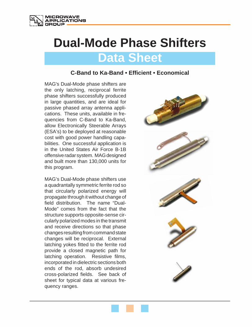
MAG's Dual-Mode phase shifters arethe only latching, reciprocal ferritephase shifters successfully producedin large quantities, and are ideal forpassive phased array antenna appli-cations. These units, available in fre-quencies from C-Band to Ka-Band,allow Electronically Steerable Arrays(ESA’s) to be deployed at reasonablecost with good power handling capa-bilities. One successful application isin the United States Air Force B-1Boffensive radar system. MAG designedand built more than 130,000 units forthis program.
MAG’s Dual-Mode phase shifters usea quadrantally symmetric ferrite rod sothat circularly polarized energy willpropagate through it without change offield distribution. The name “Dual-Mode” comes from the fact that thestructure supports opposite-sense cir-cularly polarized modes in the transmitand receive directions so that phasechanges resulting from command statechanges will be reciprocal. Externallatching yokes fitted to the ferrite rodprovide a closed magnetic path forlatching operation. Resistive films,incorporated in dielectric sections bothends of the rod, absorb undesiredcross-polarized fields. See back ofsheet for typical data at various fre-quency ranges.
MICROWAVE APPLICATIONS GROUP
3030 Industrial Parkway • Santa Maria, California 93455 • (805) 928-5711www.magsmx.com • [email protected]
Dual-Mode Phase Shifters
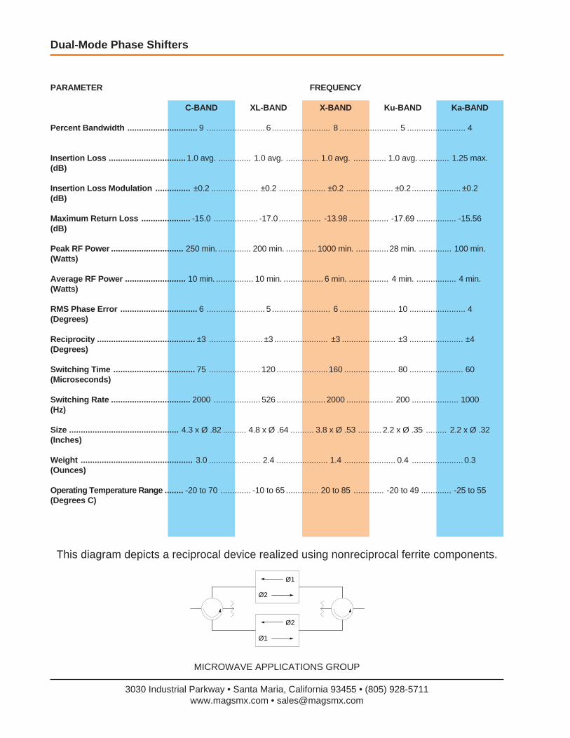
PARAMETER FREQUENCY
C-BAND XL-BAND X-BAND Ku-BAND Ka-BAND
Percent Bandwidth .............................. 9 ......................... 6 ......................... 8 ......................... 5 ......................... 4
Insertion Loss ................................. 1.0 avg. .............. 1.0 avg. .............. 1.0 avg. .............. 1.0 avg. ............. 1.25 max.(dB)
Insertion Loss Modulation ............... ±0.2 .................... ±0.2 .................... ±0.2 .................... ±0.2 ..................... ±0.2(dB)
Maximum Return Loss ..................... -15.0 ................... -17.0 .................. -13.98 ................. -17.69 ................. -15.56(dB)
Peak RF Power ............................... 250 min. .............. 200 min. ............. 1000 min. ..............28 min. .............. 100 min.(Watts)
Average RF Power .......................... 10 min. ................ 10 min. ................. 6 min. ................. 4 min. ................. 4 min.(Watts)
RMS Phase Error ................................. 6 ......................... 5 ......................... 6 ........................ 10 ........................ 4(Degrees)
Reciprocity .......................................... ±3 ....................... ±3....................... ±3 ....................... ±3 ....................... ±4(Degrees)
Switching Time ................................... 75 ...................... 120 ......................160 ...................... 80 ....................... 60(Microseconds)
Switching Rate .................................. 2000 .................... 526 ..................... 2000 .................... 200 .................... 1000(Hz)
Size ............................................... 4.3 x Ø .82 .......... 4.8 x Ø .64 .......... 3.8 x Ø .53 .......... 2.2 x Ø .35 ......... 2.2 x Ø .32(Inches)
Weight ................................................ 3.0 ...................... 2.4 ...................... 1.4 ...................... 0.4 ...................... 0.3(Ounces)
Operating Temperature Range ........ -20 to 70 ............. -10 to 65 .............. 20 to 85 ............. -20 to 49 ............. -25 to 55(Degrees C)
This diagram depicts a reciprocal device realized using nonreciprocal ferrite components.
Ø1
Ø2
Ø2
Ø1

Rotary-Field Phase ShiftersData Sheet
L-Band to Ku-Band • Unlimited Phase Shift • Highly Accurate
MAG Analog Rotary-Field FerritePhase Shifters are uniquely designedto provide unlimited phase shift withmodulo-360 degree phase controlcharacteristics that are independentof frequency, temperature, powerlevel, and ferrite material parameters.These units, available in frequencyranges from L-Band to Ku-Band, arecapable of handling high power lev-els while maintaining rms phase er-ror to less than one degree. A verysuccessful application of these unitsis the low sidelobe, single-axis scan-ning antenna of the E-3 AirborneWarning and Control System(AWACS).
Rotary-Field Phase Shifter geometryconsists of a transducer from rectan-gular to circular ceramic fi l ledwaveguide, a linear to circular polar-izer, a rotatable half-wave plate, a cir-cular to linear polarizer, and a trans-ducer back from circular to rectangularwaveguide. The phase shift angle isproportional to twice the angle ofrotation of the half-wave plate, con-trolled electronically by digital or ana-log drivers. Major design choicesinvolving ferrite material type andsize, quarter-waveplate, matchingtransformer, and driving yoke are opti-mized for specific system require-ments. See back of sheet for typicaldata at various frequency ranges.

MICROWAVE APPLICATIONS GROUP
3030 Industrial Parkway • Santa Maria, California 93455 • (805) 928-5711www.magsmx.com • [email protected]
Rotary-Field Phase Shifters
PARAMETER FREQUENCY
L-BAND S-BAND C-BAND X-BAND Ku-BAND
Percent Bandwidth ............................. 15 ..................... 12.7 ..................... 8.8 ..................... 10.5 ...................... 5.0
Average Insertion Loss ..................... 1.2 ...................... 0.6 ...................... 0.6 ...................... 0.7 ...................... 0.7(dB)
Insertion Loss Modulation ................ 0.2 ...................... 0.3 ...................... 0.3 ...................... 0.3 ...................... 0.3(dB)
Maximum Return Loss .................... -13.98 .................. -14.0 ................... -15.6 ................... -17.7 ................... -17.0(dB)
Peak RF Power ..................................... 8 ........................ 40....................... 25 ........................ 4 ......................... 2(Kilowatts)
Average RF Power ............................. 400 ..................... 600 ......................250 ...................... 60 ....................... 40(Watts)
Typical RMS Phase Error .................. 4.0 ...................... 1.0 ...................... 1.0 ...................... 1.0 ...................... 1.0(Degrees)
Switching Time .................................. 250 ..................... 300 ......................250 ..................... 200 ..................... 200(Microseconds)
Switching Time with Boost ............... 250 ..................... 100 ......................100 ..................... 100 ..................... 100(Microseconds)
Coil Current ....................................... 2400 .................... 900 ......................500 ..................... 230 ..................... 160(Milliamperes)
Coil Resistance .................................. 1.0 ...................... 1.0 ...................... 3.0 ...................... 9.5 ..................... 14.0(Ohms)
Size ............................................ 2.5 x 7.0 x 13.4 .... 2.0 x 6.6 x 8.0 ..... 2.0 x 3.0 x 4.8 ... 1.25 x 1.25 x 3.2 .. 1.0 x 1.25 x 2.0(Inches)
Weight ................................................ 282 ...................... 62....................... 30 ........................ 6 ......................... 4(Ounces)
Operating Temperature Range ..........0 to 55 ................ 0 to 50 ............... -20 to 50 ............. -40 to 70 ............. -40 to 90(Degrees C)

Synthetic Aperture Radar ComponentsData Sheet
Synthetic Aperture Radars provide extremely high resolution imagery from long ranges in all types of weather, day or night. Microwave Applications Group (MAG) provides components for several well-known Synthetic Aperture Radar systems. Among these components are MAG’s Rotary-Field Phase Shifters and MAG’s low-cost Dual-Mode Phase Shifters.
MAG Rotary-Field Ferrite Phase Shifters are uniquely designed to provide unlimited phase shift with modulo-360 degree phase control characteristics that are independent of frequency, temperature, power level, and ferrite material parameters. These units offer the advan-tage of continuously variable phase scanning and are capable of handling high power levels while maintaining rms phase error to less than one degree.
MAG Dual-Mode Phase Shifters are the only latch-ing, reciprocal ferrite phase shifters successfully produced in large quantities, and have successfully been applied to numerous military and commercial applications. These units have been proven to be much more robust and significantly less costly than active array elements, and are capable of handling moderate levels of power.
MAG provides components for the following Synthetic Aperture Radar systems:
U.S. Air Force U-2 Aircraft ASARS-2 Advanced Synthetic Aperture Radar System;
U.S. Air Force RQ-4 Global Hawk UAV Synthetic Aperture Radar;
U.K. Ministry of Defence ASTOR Sentinel R1 Airborne Stand-Off Radar;
U.S. Air Force RQ-1 Predator UAV TESAR Synthetic Aperture Radar.
MICROWAVE APPLICATIONS GROUP
3030 Industrial Parkway • Santa Maria, California 93455 • (805) 928-5711www.magsmx.com • [email protected]
Synthetic Aperture Radar Components
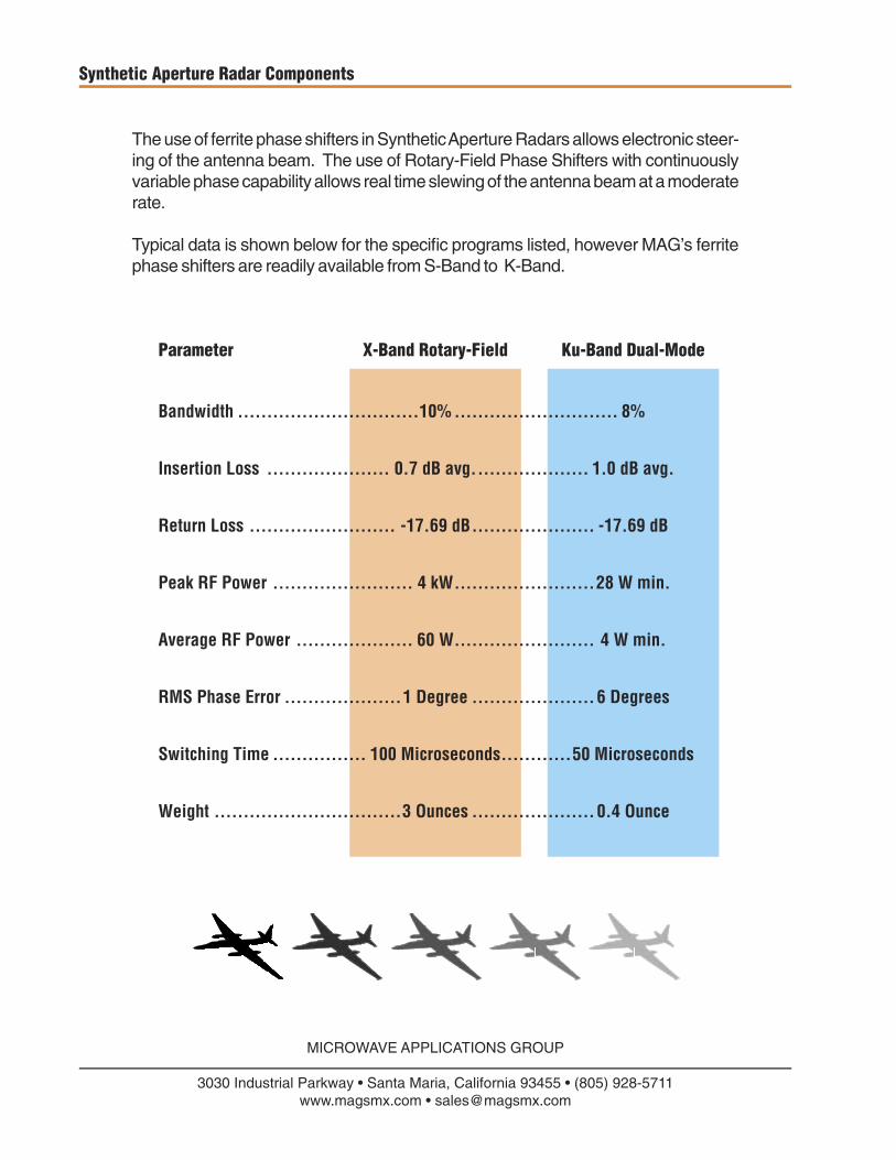
The use of ferrite phase shifters in Synthetic Aperture Radars allows electronic steer-ing of the antenna beam. The use of Rotary-Field Phase Shifters with continuously variable phase capability allows real time slewing of the antenna beam at a moderate rate.
Typical data is shown below for the specifi c programs listed, however MAG’s ferrite phase shifters are readily available from S-Band to K-Band.
Parameter X-Band Rotary-Field Ku-Band Dual-Mode Bandwidth ...............................10% ............................ 8%
Insertion Loss ..................... 0.7 dB avg. ................... 1.0 dB avg.
Return Loss ......................... -17.69 dB ..................... -17.69 dB
Peak RF Power ........................ 4 kW ........................28 W min.
Average RF Power .................... 60 W ........................ 4 W min.
RMS Phase Error ....................1 Degree .....................6 Degrees
Switching Time ................ 100 Microseconds ............50 Microseconds
Weight ................................3 Ounces .....................0.4 Ounce

Electronic Drivers for Dual-Mode Ferrite Phase ShiftersPRODUCT INFORMATION
1
1. Introduction
Early versions of the latching ferrite phaseshifters used discrete lengths of ferrite to pro-vide phase quantization. Thus, a four-bit phaseshifter consisted of cascading four sections offerrite (of length l, 2l, 4l, 8l) separated by dielec-tric spacers which provided magnetic isolation.Each individual bit operated at the maximumremanent magnetization (plus or minus) so thata simple electronic circuit was adequate to con-trol the phase shifter. However, machining andassembly of discrete ferrite sections is expen-sive. Furthermore, variations of remanent mag-netization with temperature and frequency can-not be compensated easily with this type control.Most phase shifters are now constructed from acontinuous section of ferrite with the phase shiftquantization, frequency compensation and tem-perature compensation allocated to the electronicdriver. The driver accomplishes these tasks byoperating the ferrite in a partially magnetizedstate. As the magnetization varies from nega-tive saturation to positive saturation, the rela-tive permeability of the ferrite is controlled byadjusting the magnetic flux density in the ferritecore. The flux change cycle consists of a “reset”portion plus a “phase set” portion, as indicatedby the sketches of Fig. 1. The purpose of the resetportion is to establish a reference limit-conditionof magnetization of the ferrite. The phase-setportion of the cycle meters the change of fluxaway from this reference. It is important toestablish the reference point in a repeatablemanner, since the precision of phase setting isdirectly dependent on this condition. Phase shiftis then accomplished by changing insertion phasefrom the reference point. The “memory” prop-erty of the ferrite material hysteresis loop isessential in allowing remanent-flux operation ata desired phase state, but tends to work againstestablishing a repeatable reset reference. Expe-rience has shown that there is a tendency for theapparent reset phase state to wander in a man-ner dependent on the previous phase-set historyof the unit. An improvement in the reset accu-racy can be achieved by restricting all flux changeoperations to movements around the major hys-teresis loop. Reset from a given remanent pointis accomplished by first driving to the longestphase shift end of the hysteresis loop (“full set”)and then driving to the opposite end of the loop
(“full reset”). Using this approach, adequateaccuracy is possible with the peak current levelas the criterion for terminating the full set andfull reset pulses.
The phase-set portion of the cycle uses thelevel-set signal information to achieve a par-ticular remanent flux state which correspondsto the desired insertion phase level for thephase shifter. Setting of the remanent fluxstate can be done by direct open-loop construc-tion of a driving pulse from the level-set signalor by a feedback arrangement in which infor-mation about the voltage amplitude and dura-tion of an applied pulse is accumulated, com-pared with the level-set signal, and used toterminate the drive at the appropriate time.The simplest relationship of either type is onein which the Volt-time integral of the drivingpulse is made to be proportional to the desiredphase shift angle. In practice, it is necessaryto calibrate the Volt-time integral to fit theactual phase shifter characteristics, and evento change this calibration as a function ofoperating frequency and temperature.
Figure 1. Flux Change Cycles.
Ø
Ι
A
B C
D
RESET A B CSET C D
Ø
Ι
A
B
C D
FULL SET-RESET A B C DSET D E
E
a. RESET-SET SWITCHING
b. FULL SET-RESET SWITCHING

Electronic Drivers for Dual-Mode Ferrite Phase Shifters
3030 Industrial Pkwy. / Santa Maria, CA. 93455 / (805)928-5711 / FAX (805)925-5903
2
is set by measuring the volt-time product associ-ated with the phase shifter SET pulse. Althoughthe supply voltage is approximately constant, varia-tions affect phase shifter performance unless com-pensation is provided. The MAG driver providesthis compensation by sampling the phase shiftercontrol voltage and digitally integrating the sampledvoltage to provide accurate characterization of thevolt-time product.
Using the digital integration described above, anew logic chip was developed using 5 Volt CMOSstandard cells. The Application Specific IntegratedCircuit (ASIC) chip provided the logic necessary tocontrol four phase shifters. Built-in-test (BITE)was also incorporated into the driver to allow diag-nostic testing of the driver and phase shifter. Toprove the design, a breadboard was built usingLSTTL logic. After verification of the design, thechip was physically realized in September 1988.
3.2 Driver Features
The driver provides the usual control waveformsfor latching dual-mode ferrite phase shifters, e.g., asaturated reset pulse followed by a timed set pulse.The time of the set pulse is determined by the dataword and the voltage applied to the phase shifterdrive coils. The driver provides these waveformsfor all channels simultaneously in the case of mul-tichannel drivers.
Special features incorporated into the driver are:
Built-in-test circuits which provide for thesensing of the set and reset currents in eachchannel and provide an indication of afailure.
If a particular channel does not receive anew data word (parallel) or receives dataword zero (serial), the output drivers arenot activated during the switching cycle.
Automatic shutdown of the driver limitsthe maximum set current, which protectsthe set output circuit if the phase shiftersaturates.
The driver requires two power supplies. The first isthe logic supply of 5 Volts which must be wellregulated since this voltage is also the reference
2. Phase Shifter Control Characteristics
A typical control characteristic of a latching phaseshifter and its electronic driver is shown in Fig. 2.The control characteristic will vary from phaseshifter to phase shifter. Also, changing the r-ffrequency or the ambient temperature will causechanges in the control characteristic. In order toaccurately set the phase shifter, calibration curvesfor each device at various operating frequenciesand temperatures are measured and stored eitherin the beam steering computer or in PROM at thedriver itself. Errors of the order of three degreesrms are achievable for a 7-bit device over a tenpercent frequency range and a temperature rangeof 90 degrees Celsius.
3.1 MAG Driver Developments
For the past few years, MAG has been investigatingmethods of reducing driver cost. Removal of therequirements to mount the driver directly to thephase shifter has allowed us to bundle several driv-ers into one hybrid package with the very desirableeffect of reducing both cost, size and weight.
To accurately establish to state of a ferrite phaseshifter, the magnetic flux in the microwave ferrite
0
50
100
150
200
250
PHAS
E SH
IFT
(DEG
REES
)
300
350
400
0 32 64 96
DRIVER INPUT COMMAND
127 159 191 223 255
Figure 2. Control Characteristic of a LatchingPhase Shifter.

3
Electronic Drivers for Dual-Mode Ferrite Phase Shifters
VALID
VALID
ADDRESS
DATA LOAD
OUTPUT ENABLE
BITE
DATA
RESET SET
hd
sd
w
ha
doe Rmax Smax
t
tt
t
t
>100ns
>50ns
>50ns
>50ns
t > >t
>50ns
t α previous set data
t ≈ constant
D0Dn - 1
DnD4D3D2D1DATA
BITE
CLOCK
OUTPUT ENABLE
t α previous set data
t ≈ constant
Smaxt>
Rmaxt>
RESETSETt >50nshdt sc >50ns
t S
t cd >50ns
OPTION CLOCK/BITEOR OUTPUT ENABLE
a. PARALLEL DATA
b. SERIAL DATA
Figure 3. Timing Diagrams.
voltage for the A/D converter used in theASIC to measure volt-time product. Thesupply must furnish 25 mA current to eachASIC connected to it. The second supply –which may have poor regulation – is thesupply used to provide switching energy tothe phase shifter. Since the phase shifter is alatching device, it only requires drive energywhen it is desired to change the phase state.To reduce the peak current demands on thesecond power supply, local energy storage isprovided by a capacitor located at the driver.Typically, the second power supply operatesat 15 Volts. The current from this supply isdependent upon the geometry of the phaseshifter being controlled and the switchingrate of the phase shifter. The driver can beswitched at rates up to 2 KHz.
The driver operates by sensing the reset cur-rent and turning off the voltage once the resetcurrent has reached a given value – typicallyin the range 1.2 to 1.8 Amp. The set currentis also sensed and the set circuit is protectedby shutting off the driver whenever this cur-rent exceeds a predetermined limit. Thethreshold currents for the BITE circuits are750 mA for the reset and 150 mA for the set.
Data is supplied to the driver via digital inputsignals. The logical low is between 0 and 1.5 Voltswhile the logical high is between 3.5 and 5.0 Volts.The input current in either the low or high state isless than or equal to 10 microamperes. Data may beentered using either a parallel or serial mode.
The parallel mode uses an 8-bit data bus and anaddress bus whose size is commensurate with thenumber of drivers connected to the data bus, i.e., a4-bit address bus is sufficient to separately address16 channels. Data on the data bus will be loaded tothe address specified by the address bus upon theapplication of a signal to the data load (DL) line.The timing diagram is given in Fig. 3a. The maxi-mum rate that data may be loaded is 5 MHz. Thereset-set switching cycle is initiated by applicationof a signal to the output enable (OE) line.
The serial mode of operation requires the data to beentered into a latch on the driver via a clock signal.The maximum clock frequency is 5 MHz. The reset-set switching cycle may be initiated by the coinci-dence of the clock and the data or by a signal on anoutput enable (OE) line as shown in Fig. 3b.
3.3 Driver Packaging
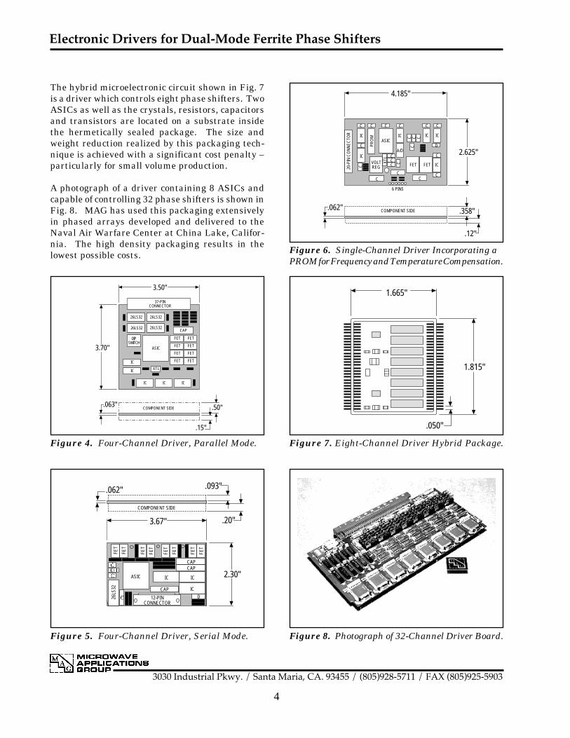
MAG has developed several techniques for packag-ing the logic chip and the associated power stages.The least costly of these uses discrete componentsmounted on a circuit board. The ASIC is mountedin a package which is hermetically sealed. Fig. 4shows a realization of a four-channel driver whichuses a parallel interface and Fig. 5 shows a four-channel driver using a serial interface. It is obviousthat the serial interface results in a significantreduction in size at the cost of increased dataloading time. What is not so obvious is the fact thatthe serial configuration results in increased reli-ability because of the fewer connections involved.
A phased array antenna will normally have a beamsteering computer (BSC) which allows for tempera-ture and frequency compensation required by thephase shifter. However, in some cases it is desir-able to include memory on the driver to provide thenecessary compensation. The single-channel drivershown in Fig. 6 uses discrete components andPROM storage to provide frequency and tempera-ture compensation.
Electronic Drivers for Dual-Mode Ferrite Phase Shifters
3030 Industrial Pkwy. / Santa Maria, CA. 93455 / (805)928-5711 / FAX (805)925-5903
4
Figure 5. Four-Channel Driver, Serial Mode. Figure 8. Photograph of 32-Channel Driver Board.
Figure 4. Four-Channel Driver, Parallel Mode.
Figure 6. Single-Channel Driver Incorporating aPROM for Frequency and Temperature Compensation.
Figure 7. Eight-Channel Driver Hybrid Package.
26LS32 26LS32
26LS32 26LS32
DIPSWITCH
ASIC
CAP
IC IC IC
IC
IC XTL
FET FET
FET FET
FET FET
FET FET
37-PINCONNECTOR
.50".063"
.15"
COMPONENT SIDE
3.70"
3.50"
1.815"
1.665"
.050"
COMPONENT SIDE
.20"
2.30"
.093"
3.67"
FET R
ICASIC
12-PINCONNECTOR
CAP
26LS
32
FET
FET
FET
FET
FET RR
CAP CAP
IC
IC
D
FET
FET
.062"
C
D
CC
C
C
C
CCCCCC
CCC
XTL
20-P
IN C
ON
NEC
TOR
ASIC
FET FET
A/D
IC
IC
IC
ICICIC
PRO
M
6 PINS
4.185"
2.625"
COMPONENT SIDE .358"
.12"
.062"
C C CC
C
C
VOLTREG
The hybrid microelectronic circuit shown in Fig. 7is a driver which controls eight phase shifters. TwoASICs as well as the crystals, resistors, capacitorsand transistors are located on a substrate insidethe hermetically sealed package. The size andweight reduction realized by this packaging tech-nique is achieved with a significant cost penalty –particularly for small volume production.
A photograph of a driver containing 8 ASICs andcapable of controlling 32 phase shifters is shown inFig. 8. MAG has used this packaging extensivelyin phased arrays developed and delivered to theNaval Air Warfare Center at China Lake, Califor-nia. The high density packaging results in thelowest possible costs.

MICROWAVEAPPLICATIONSGROUP
1
Background
Microwave Applications Group (MAG) is well known as a supplier of ferrite microwave phase control devices since the 1960’s. The United States Air Force AWACS E-3 Sentry antenna and B-1B AN/APQ-164 offensive radar system along with many other programs have used ferrite devices developed, designed, and produced by MAG. Beginning in the 1990’s, we applied our experience to microwave switching devices. These switches use the principle of Faraday rotation to achieve a unique combination of high isolation, wide temperature range, and reciprocal operation at moderately high power levels. A broad introduction to the principles involved is presented here, followed by examples of our delivered switch products. MAG’s design capability extends well beyond these examples, and we invite inquiries regarding other specific applications.
Introduction to Faraday Rotation Switches
Faraday rotation is fundamental to all microwave ferrite control devices. In its simplest form, shown in Figure 1, Faraday rotation describes the phenomenon in which the polarization of an electromagnetic plane wave rotates nonreciprocally as it travels through an infinite ferrite medium that is magnetized along the direction of propagation. At a given frequency the amount of rotation per unit length depends on (1) the activity of the ferrite material, and (2) the strength of the applied magnetic bias field.
Practical devices can use a metallized ferrite rod which forms a fully-filled circular
Product Information
Microwave Waveguide
SwitchesBackground p 1
Introduction to Faraday Rotation Switches p 1
Electronic Control p 3
Manufacturing and Quality Controls p 4
X-Band Basic SPDT Switch p 5
C-Band High Power SPDT Switch p 6
X-Band SP3T Switch p 7
X-Band DPDT Switch p 8
X-Band SPDT Reciprocal Switch p 9
X-Band SPDT Tandem-Rotator Reciprocal Switch p 10
X-Band DPDT Circulator Switch p 11
Summary and Continuing Developments p 12
Figure 1 - Faraday Rotation Concept

MICROWAVEAPPLICATIONSGROUP
2
waveguide. When a bias magnetic field is applied along the axis of the rod, the polarization plane of a linearly polarized TE11-mode will rotate as the wave propagates along the rod. The amount and direction of the rotation can be controlled by the magnitude and direction of the bias magnetic field; however, the relative insertion phase of the wave depends only on the magnitude of the applied bias field. A matched pair of rods both biased to produce 90 degrees of rotation will have exactly zero insertion phase difference if the rotation directions are the same, and, because of the reversal of the polarization plane, exactly 180 degrees of insertion phase difference if the rotation directions are opposite. Such a matched pair of rods can be assembled into a microwave bridge circuit using folded hybrid tees to form a reciprocal switch. High isolation between the outputs and operation at high peak and average power levels are possible with this type of switch. Figure 2 shows a block diagram of a basic switch bridge circuit configuration.
As noted above, the insertion phase difference between the matched pair of rods will remain constant; this applies even though the amount of Faraday rotation may change from the optimum 90 degree value. Such deviations may be caused by frequency and temperature variation, and result in a small amount of cross-polarized power at the output of the rotator sections. This cross-polarized power is typically absorbed in a film load or in a high power load placed in the side arm of an orthomode transducer (OMT). Thus the basic switch isolation is fairly insensitive to changes of frequency and temperature, with the main effect of shifts of rotation away from the optimum value being a small increase of insertion loss.
Figure 2 - Basic Switch Block Diagram

Product Information • Microwave Waveguide Switches
3
Electronic Control
The state of each Faraday rotator is determined by the magnitude and direction of the magnetic bias flux along the axis of the rotator ferrite rod. External ferrite pieces placed in contact with the rotator rod form a closed magnetic path so that the bias flux can be maintained as a remanent condition with no continuous power required. State changes are commanded by voltage pulses applied to a coil wound around the rotator rod in the space between the rod and the external magnetic return path pieces.
T h e h y s t e r e s i s l o o p s h o w n i n Figure 3 represents the B-H characteristic in the rotator rod with external return path elements. In this drawing, State 1 and State 2 are the remanent (“latched”) operating points that provide equal magnitudes and opposite directions of bias magnetic flux. Note that the total magnetic flux is the flux density B integrated over the transverse-plane area of the rotator rod. These states should correspond to clockwise and counterclockwise rotations of 90 degrees in the rod. To switch between the two states, a voltage of the correct polarity is applied to the coil and the flux in the rod changes at a rate directly proportional to the instantaneous applied voltage and inversely proportional to the number of turns in the coil.
The coil current is proportional to H integrated over the length of the closed magnetic path. Since H=0 at State 1 and State 2, no steady current is needed in the quiescent case. Current will flow during the switching transient because H is nonzero. The magnitude of the current waveform
Figure 3 - Hysteresis Loop

MICROWAVEAPPLICATIONSGROUP
4
versus time will generally have the shape shown in Figure 4, with the points a through e matching the designations on the hysteresis loop of Figure 3. The voltage pulse ends at point d when the current reaches a preset level.
Although one of the two rotator channels of the basic switch remains at the same state, its coil is pulsed with the same voltage polarity during each switching operation. Because the flux density level of the ferrite for this channel is already at the knee of the hysteresis loop, the current will rise rapidly to the preset value for terminating the voltage pulse. Sensing of the current rise to the preset limit in both channels is typically used as an indication that the ferrite is being switched normally, and a built-in-test (BIT) error signal is generated when the desired current limit is not sensed in a channel.
Manufacturing and Quality Controls
Products delivered by MAG must meet stringent requirements of mechanical characteristics and electrical performance. Engineering drawings define the product through various stages from raw material through final assembly. Manufacturing process and procedure documents define the detailed steps in the production flow. Acceptance test procedures define the electrical tests performed to demonstrate compliance with customer and/or MAG specifications. All documentation is reviewed and approved by MAG Engineering prior to release. Finally, MAG has a Quality System approved to MIL-I-45208A and meeting the intent of ISO 9002.
Figure 4 - Current Waveform

Product Information • Microwave Waveguide Switches
5
X-Band Basic SPDT Switch
The photograph to the left shows the first product example, which uses the bridge circuit described above and operates at X-Band. The specific application is an aircraft landing approach system. The switch connects a transmit-receive port reciprocally to azimuth or elevation antennas. Because the power levels are moderate, a film load is used to absorb cross-polarized error power.
Two electronic driver circuits are located on a printed wiring board incorporated into the switch housing. One of the drivers switches between two saturated states (State 1 and State 2) of the hysteresis loop as depicted in Figure 3 above. This driver controls the lower Faraday rotator in the bridge circuit of Figure 2 above, causing rotation of either +90 or -90 degrees corre-sponding to State 1 or State 2. The other driver is always commanded to State 1 which sets this rotator to +90 degrees. The coil current is monitored for each driver to detect magnetic saturation in the ferrite by sensing a predetermined current amplitude. Once this level is reached, the drive voltage is removed and the ferrite relaxes to the remanent “latched” state. Each driver contains BIT circuitry to verify that a current pulse has occurred. The BIT signals are ANDed to form a composite signal.
The rotators and drivers are mounted in an environmentally sealed housing. WR90 waveguide flanges and a standard bulkhead connector provide the RF and electrical connections to the switch.
X-Band Basic SPDT Switch
50 kW Peak Power 0.5 dB Max Insertion Loss
17 dB Max Return Loss
25 dB Min Isolation
Less than 50 µsec Switching Time
4 KHz Switching Rate
2% Bandwidth
Operating Temperature Range -29° to +49°C

MICROWAVEAPPLICATIONSGROUP
6
C-Band High Power SPDT Switch
Our second product example is shown in the photograph to the right, and is a higher power reciprocal single input port, dual output port switch for use in C-Band Doppler weather radar systems. The switch is used to commutate the polarization of the RF energy transmitted and received by the radar system between vertical and horizontal. This feature allows the weather forecaster to form a better interpretation of the radar returns and thereby distinguish between rain, hail and snow.
The block diagram for this switch is the same as that of the X-Band single input, dual output switch described on the previous page. However, the peak and average operating power levels are much higher, and film loads are not able to handle the cross-polarized error power. Instead, orthogonal mode transducers are placed at the outputs of the Faraday rotator sections. Dummy loads capable of absorbing the error power for deviations from the ideal 90 degree rotation case are installed in the side arms of the OMT’s.
As in the X-Band switch on the previous page, the Faraday rotators require no continuous power in the quiescent condition. Functioning of the electronic driver is essentially the same, with BIT signals available to verify that the proper current pulse has occurred during the transient condition.
C-Band High Power SPDT Switch
300 kW Peak Power
300 W Average Power
0.6 dB Insertion Loss
20 dB Max Return Loss
30 dB Isolation
Less than 50 µsec Switching Time
1.5 KHz Switching Rate
4% Bandwidth
Operating Temperature Range -40° to +50°C

Product Information • Microwave Waveguide Switches
7
X-Band SP3T Switch
The next product example is a single input, triple output reciprocal switch for fire-control radar systems at X-Band.
Input power is split equally into two channels using an H-plane folded hybrid tee. Signals in each channel pass through two tandem one-bit, latching Faraday rotators which each impart either +45 degrees rotation or -45 degrees rotation. Based on the combination selected, the outputs of the tandem rotators will be -90, zero, or +90 degrees of rotation. The outputs of these channels are connected to OMT’s. Selecting zero net rotation in both channels causes the RF signals to appear at the through arms of the OMT’s and be summed at one arm of a following hybrid tee junction. Selecting ±90 degree rotation causes the RF signals to appear at the side arms of the OMT’s and be summed in a following hybrid tee in one of the two output arms if the rotation senses are equal and in the other arm if the senses are opposite.
Because the magnitude of the magnetic bias field is the same in each of the tandem rotators, the overall insertion phases of the two channels will tend to track each other over frequency and temperature. However, drive compensation over temperature is necessary to avoid degradation of isolation caused by deviation of the rotation amounts from optimum. The currents in each winding are sensed for the BIT circuit and the lack of proper current in any winding will cause an error to appear at the BIT output.
X-Band SP3T Switch
25 kW Peak Power
250 W Average Power
1 dB Max Insertion Loss
15 dB Max Return Loss
20 dB Min Isolation
Less than 50 µsec Switching Time
1.2 KHz Switching Rate
10% Bandwidth
Operating Temperature Range -40° to +71°C

MICROWAVEAPPLICATIONSGROUP
8
X-Band DPDT Switch
The next example of a switch configuration is a duplexing, high isolation X-Band four-port unit for a naval application. This four-port device is designed for transmitted input, received output, and two selectable antenna output ports (Azimuth and Elevation), and mates with UG-138/U waveguide flanges. The complete package consists of a bridge-type four-port switchable circulator with two bridge-type reciprocal switches in the antenna output lines to increase the isolation to the unselected antenna. The four-port circulator uses a folded hybrid tee at the input to divide the power equally into two channels. One channel contains a 90 degree waveguide twist followed by a zero degree rotator. The other channel contains a compensating length of ordinary waveguide followed by a ±90 degree switchable rotator. The reciprocal isolating switches use the basic switch block diagram of Figure 2 above, with one of the two outputs simply connected to a dummy load.
The electronic control circuits are housed integral with the RF switch housing. Two TTL logic level control signals are required for the switch. The first control signal uses a high level (5 Volts) to select one port and a low level (0 Volts) to select the other port. The other control signal is the switching pulse which initiates the switching se-quence. The currents in each winding are sensed for the BIT circuit and the lack of proper current in any winding will cause an error to appear at the BIT output.
X-Band DPDT Switch
200 kW Peak Power
1.5 dB Max Insertion Loss
Less than 20 dB Return Loss
58 dB Isolation Transmitter to Idle
Less than 50 µsec Switching Time
4 KHz Switching Rate 4% Bandwidth
Operating Temperature Range -15° to +55°C

Product Information • Microwave Waveguide Switches
9
X-Band SPDT Reciprocal Switch
This switch has a high average power requirement coupled with an impressive 11% bandwidth. The tradeoff of a higher isolation requirement, but at lower peak power levels, allows use of a resistive film load to absorb cross-polarized error signals, simplifying construction. MAG’s bridge-type switch construction in an al-ternate packaging concept is used for this application.
This reciprocal device uses a very com-pact E-plane tee for the input, which equally splits the applied signal. One of the rotators is always commanded to +90 degrees, while the other is commanded to ±90 degrees depending on the output port desired. The outputs of the two rotators are combined in a very compact H-plane hybrid tee equivalent known as an ortho-tee. This configuration allows the switch to be located immediately behind the rotary joint in the particular application for this unit, requiring very little additional wave-guide to interface to the two antennas.
This switch uses MAG’s driver compen-sation circuit to maintain the optimum rotation setting over a 110 degree Celsius temperature range. The driver allows the switch to provide very good isolation between the two channels over the entire temperature band. The two collocated drivers contain BIT circuitry to verify that the rotator windings receive the correct current pulse.
X-Band SPDT Reciprocal Switch
10 kW Peak Power
350 W Average Power
0.75 dB Max Insertion Loss
19.09 dB Max Return Loss
30 dB Min Isolation
Less than 20 µsec Switching Time
2.5 KHz Switching Rate
11% Bandwidth
Operating Temperature Range -55° to +55°C
MICROWAVEAPPLICATIONSGROUP
10
X-Band SPDT Tandem-Rotator Reciprocal Switch
The X-Band Tandem-Rotator Reciprocal Switch uses zero degree and 90 degree total Faraday rotation states to achieve reciprocal connections to the desired ports. This structure operates at moder-ate isolation levels and moderate peak and average power levels compared with MAG bridge-type switches, but provides a smaller and less expensive package. The beauty of this switch is its compact size (6.18 inches / 156.9 mm long x 2.3 inches / 58.4 mm wide x 2.84 inches / 72.1 mm high), and light weight (1.6 pounds / 726 grams).
The simplicity of this switch is achieved by using a single rotator element, thereby eliminating the need for input and output tees. The zero degree and 90 degree states drive into either port of an OMT.
The driver is a mature design with com-pensation to maintain proper rotation over the operating temperature range. A BIT circuit is included providing switch status information.
X-Band SPDT Tandem-Rotator Reciprocal Switch
50 kW Peak Power
100 W Average Power
0.5 dB Max Insertion Loss
17.7 dB Max Return Loss
25 dB Min Isolation
Less than 25 µsec Switching Time
2 KHz Switching Rate
12% Bandwidth
Operating Temperature Range -30° to +60°C

Product Information • Microwave Waveguide Switches
11
X-Band DPDT Circulator Switch
This switch uses two reciprocal elements to achieve nonreciprocal operation. The device is essentially a bridge-type four-port switchable circulator. Although either input port can be used with the resultant return signal appearing at the other, this particular device is configured for VSWR monitoring of the reflected signal using just one input.
Input power is equally split into two channels using an H-plane folded hybrid tee. One channel contains a 90 degree waveguide twist followed by a ±90 degree switchable rotator. The other channel contains a compensating length of ordi-nary waveguide followed by a zero degree rotator. Use of the twist section achieves the nonreciprocal action desired for this application. The peak and average power requirements of the device necessitate placement of OMT’s at the rotator outputs. The two OMT outputs are applied to the colinear ports of a folded H-plane tee and the two orthogonal arms act as the respec-tive antenna interfaces. The offport of the input tee will see any received signal, but in this case it is used for VSWR monitoring of the two antennas.
Driver compensation to maintain the optimum rotation over the operating tem-perature for each element is utilized to avoid degradation of the isolation caused by incorrect rotation values. The current in the windings of each rotator element is monitored by a BIT circuit. As a safety mechanism, an error signal will appear at the BIT output if current is lacking at either or both windings.
X-Band DPDT Circulator Switch
75 kW Peak Power
400 W Average Power
0.85 dB Max Insertion Loss
17.7 dB Max Return Loss
25 dB Min Isolation
Less than 35 µsec Switching Time
4 KHz Switching Rate
9% Bandwidth
Operating Temperature Range -40° to +85°C

Product Information • Microwave Waveguide Switches
MICROWAVE APPLICATIONS GROUP
3030 Industrial Parkway • Santa Maria, California 93455 • (805) 928-5711www.magsmx.com • [email protected]
12
Summary and Continuing Developments
Whether constant current or latching con-figuration, MAG’s ferrite based waveguide switches are available from Ka-Band to L-Band, and provide good channel to channel isolation and insertion loss at moderate peak and average RF power levels.
The bridge-type switch can be realized as either reciprocal or nonreciprocal with a slight length adjustment, and can oper-ate in either a single pole or double pole configuration with only a small impact on the isolation between the two input ports. Bridge-type switches are available in DT, 3T, or 4T variations.
MAG developed compact tandem-rotator switches as a means of providing perfor-mance similar to the bridge-type switch, but at a more economical price. MAG is currently developing a switching circula-tor design as another alternative in a cost driven environment.
Our goal is finding cost effective solutions to meet customer specifications. Contact MAG and utilize our experience in order to fulfill the needs of your RF switch re-quirement.
C-Band Constant CurrentSPDT Switch
X-Band Constant CurrentDP4T Switch

MICROWAVEAPPLICATIONSGROUP
Roll ResolversProduct Information
Waveguide Ferrite Modulator Control Devices
MICROWAVE COMPONENTS AND SUBSYSTEMS SINCE 1969
Microwave Applications Group (MAG) has designed, produced, and delivered waveguide ferrite modulator control devices to compensate for motion while an aircraft is in fl ight and its radar system is in use. Commonly referred to as a “Roll Resolver,” these units are in service currently on two well-known plat-forms.
The Roll Resolver functions by performing a rotation of coordinates from the reference set at the input of the network to a rotated set at the output of the network. This is accomplished using the circuit shown below. When one phase shifter is set to angle φ and the other to the angle –φ, the output of the circuit (OUT) expressed in terms of the input at the elevation port (EL) and the input at the azimuth port (AZ) may be shown to be
OUT = EL cos (φ) – AZ sin (φ).
This is the true vertical signal from the monopulse an-tenna, which has undergone a roll of φ degrees. The true horizontal signal may be found by setting the phase shifters to command angles ±φ±π/2.
The phase shifters shown in the schematic diagram are realized using MAG designed and produced Ro-tary-Field phase shifters. This type of ferrite phase shifter has very good phase accuracy and exhibits low
SHORTSLOTHYBRID
FOLDEDH-PLANETEE
φ
φ
ELEVATION
AZIMUTH
OUTPUT

MICROWAVEAPPLICATIONSGROUP
3030 Industrial Parkway • Santa Maria, California 93455 • (805) 928-5711www.magsmx.com • [email protected]
Roll Resolvers
insertion loss and insertion loss modulation. A matched set of phase shifters and the elec-tronic circuitry required to control the phase shifters are assembled into an aluminum hous-ing. The short slot hybrid and the folded H-plane tee are bolted to the housing to form a rugged assembly shown in the photograph on the front page. The depicted unit is repre-sentative of the Roll Resolvers which continue to operate successfully on board the U.S. Air Force’s B-1B bombers. A similar device is in use with the Air Force’s B-2 bomber fl eet.
Microwave Applications Group has a proven record of creativity and innovation in microwave component and subsystem design for government, military, and commercial applications. MAG has been at the forefront of electronically-steered radar technology, especially in the area of ferrite-based devices. Programs utilizing MAG designed and produced products over the last 30 years are well-known and continue to operate successfully. Examples of products developed and supplied by MAG are:
Precise analog ferrite phase shifters for use at high peak and average power levels;
Reciprocal, latching, ferrite phase shifters with weight and size parameters compatible for use in phased array antennas;
Compact, high performance phase shifters for use in sequential lobing of array antennas;
High performance waveguide isolators, variable power dividers, and polarization controllers;
Ferrite switches that achieve a unique combination of high isolation, wide temperature range, and reciprocal operation at high power levels;
Electronic drivers, function generators and interface equipment for real-time computer control of processes;
Planar phased array antennas and linear array modules, complete with phase shifters, drivers, antenna controller, radiating elements and feed assembly;
Multi-channel driver packages with the capability to drive a set of phase shifters.
MAG continues to develop new products using proven ferrite technology, and looks forward to advancing the state of the art of microwave components and subsystems.

MICROWAVEAPPLICATIONSGROUP
Electronic Scanning AntennasProduct Information
Microwave Applications Group (MAG) has a proven record of creativity and innovation in microwave component and subsystem design for government, military, and commercial applications. MAG has been at the forefront of electronically-steered radar technology, especially in the area of ferrite-based devices. Programs utilizing MAG designed and produced products over the last 30 years are well-known and continue to operate successfully. In more recent years, MAG has designed and built Electronically Scanning Antennas, utilizing years of component-level experience combined with engineering expertise. The following pages provide data on these antennas produced by MAG:
Phased Array Antenna System (PAAS), C-Band, X-Band, Ku-Band
I-30 Expedient Antenna System, X-Band
Terminal Guidance Antenna, Ku-Band
Planar Phased Array Antenna, Ku-Band
Millimeter-Wave Antenna, Ka-Band

Microwave Applications Group
LIFTING�SWIVEL�RING, 5 PL
36 1/8±3/4
40 3/4±3/4 1 1/2 36±23 3/16±1/4
20 1/8±1
WR62 CHOKE FLANGE�(RF INPUT)
I/O PANEL��FIBEROPTIC�FILTERED AC �IN DATA�CONNECTOR
1/2-13 UNC-2A�LIGHTNING�GROUND LUG
COOLING AIR INLETS
ENVIRONMENTALCOVER OVER
RADIATINGAPERTURE
HANDLE�4 PL
SCHRAEDER VALVE�(INTERNAL SYSTEM�PRESSURE)
±1/2, 2 PL
Phased Array Antenna System (PAAS), C-Band, X-Band, Ku-Band
Designed for test range instrumentation applications, the Phased Array Antenna System (PAAS) is a family of rugge-dized, low-cost electronically scanning antennas.
The antenna portion of the system is made up of a phased array transmission lens (bootlace lens) with a space feed. The lens consists of aperture and feed plates with fer-rite phase shifters contained between the two plates. Radiating elements integrated into the aperture and feed plates are distributed on an equilateral triangular grid. The element spacing is selected to ensure that grating lobes do not occur in visible space when the beam is scanned to its limits, and the triangular grid geometry is used to minimize the number of elements.
In addition to the antenna portion, the system also consists of a beam steering controller (BSC). The BSC accepts signals from the system controller and points the antenna main beam in a specifi ed direction within a 60 degree cone about the antenna normal. Digital communication between the BSC and the antenna is accomplished via a fi beroptic network.
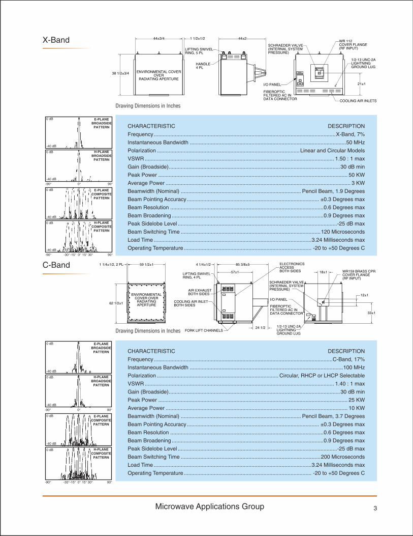
The mechanical and electrical characteristics, physical dimensions and interface data, as well as measured patterns are presented for the Ku-, X-, and C-Band PAAS antennas.
Ku-Band
Drawing Dimensions in Inches
CHARACTERISTIC DESCRIPTION
Frequency .......................................................................................................................Ku-Band, 7%
Instantaneous Bandwidth ......................................................................................................100 MHz
Polarization ................................................................................. Circular, RHCP or LHCP Selectable
VSWR .............................................................................................................................. 1.40 : 1 max
Gain (Broadside) ..................................................................................................................30 dB min
Peak Power .............................................................................................................................. 30 KW
Average Power ........................................................................................................................1500 W
Beamwidth (Nominal) ................................................................................ Pencil Beam, 3.7 Degrees
Beam Pointing Accuracy ........................................................................................ ±0.3 Degrees max
Beam Resolution ......................................................................................................0.6 Degrees max
Beam Broadening .....................................................................................................0.9 Degrees max
Peak Sidelobe Level ..........................................................................................................-25 dB max
Beam Switching Time .............................................................................................120 Microseconds
Load Time .........................................................................................................3.24 Milliseconds max
Operating Temperature ..................................................................................... -20 to +50 Degrees C
15° 30°0°
0 dB
-40 dB
0 dB
-40 dB-90°
0 dB
-40 dB
0 dB
-40 dB-15°-90° -30°
0°
H-PLANEBROADSIDE
PATTERN
E-PLANEBROADSIDE
PATTERN
90°
E-PLANECOMPOSITE
PATTERN
H-PLANECOMPOSITE
PATTERN
90°
2
Microwave Applications Group
I/O PANEL��FIBEROPTIC�FILTERED AC IN�DATA CONNECTOR
SCHRAEDER VALVE�(INTERNAL SYSTEM�PRESSURE)
44±3/4 1 1/2±1/2
38 1/2±3/4 ENVIRONMENTAL COVEROVER
RADIATING APERTURE
44±2
21±1
LIFTING SWIVEL�RING, 5 PL
HANDLE�4 PL
WR 112�COVER FLANGE�(RF INPUT)
1/2-13 UNC-2A�LIGHTNING�GROUND LUG
COOLING AIR INLETS
X-Band
Drawing Dimensions in Inches
CHARACTERISTIC DESCRIPTION
Frequency .........................................................................................................................X-Band, 7%
Instantaneous Bandwidth ........................................................................................................50 MHz
Polarization ............................................................................................... Linear and Circular Models
VSWR .............................................................................................................................. 1.50 : 1 max
Gain (Broadside) ..................................................................................................................30 dB min
Peak Power .............................................................................................................................. 50 KW
Average Power ........................................................................................................................... 3 KW
Beamwidth (Nominal) ................................................................................ Pencil Beam, 1.9 Degrees
Beam Pointing Accuracy ........................................................................................ ±0.3 Degrees max
Beam Resolution ......................................................................................................0.6 Degrees max
Beam Broadening .....................................................................................................0.9 Degrees max
Peak Sidelobe Level ..........................................................................................................-25 dB max
Beam Switching Time .............................................................................................120 Microseconds
Load Time .........................................................................................................3.24 Milliseconds max
Operating Temperature ..................................................................................... -20 to +50 Degrees C
C-Band
Drawing Dimensions in Inches
CHARACTERISTIC DESCRIPTION
Frequency .......................................................................................................................C-Band, 17%
Instantaneous Bandwidth ......................................................................................................100 MHz
Polarization ................................................................................. Circular, RHCP or LHCP Selectable
VSWR .............................................................................................................................. 1.40 : 1 max
Gain (Broadside) ..................................................................................................................30 dB min
Peak Power .............................................................................................................................. 25 KW
Average Power ......................................................................................................................... 10 KW
Beamwidth (Nominal) ................................................................................ Pencil Beam, 3.7 Degrees
Beam Pointing Accuracy ........................................................................................ ±0.3 Degrees max
Beam Resolution ......................................................................................................0.6 Degrees max
Beam Broadening .....................................................................................................0.9 Degrees max
Peak Sidelobe Level ..........................................................................................................-25 dB max
Beam Switching Time .............................................................................................200 Microseconds
Load Time .........................................................................................................3.24 Milliseconds max
Operating Temperature ..................................................................................... -20 to +50 Degrees C
SCHRAEDER VALVE�(INTERNAL SYSTEM�PRESSURE)
I/O PANEL��FIBEROPTIC�FILTERED AC IN�DATA CONNECTOR
1/2-13 UNC-2A�LIGHTNING�GROUND LUG
WR159 BRASS CPR�COVER FLANGE�(RF INPUT)
62 1/2±1
59 1/2±1
ENVIRONMENTALCOVER OVER
RADIATINGAPERTURE
85 3/8±54 1/4±1/2
24 1/2
LIFTING SWIVEL�RING, 4 PL
AIR EXHAUST�BOTH SIDES
COOLING AIR INLET�BOTH SIDES
33±1
12±1
18±157±1
1 1/4±1/2, 2 PL
FORK LIFT CHANNELS
ELECTRONICS�ACCESS�BOTH SIDES
0 dB
-40 dB
0 dB
-40 dB
-90°
0 dB
-40 dB
0 dB
-40 dB
E-PLANEBROADSIDE
PATTERN
H-PLANEBROADSIDE
PATTERN
E-PLANECOMPOSITE
PATTERN
H-PLANECOMPOSITE
PATTERN
-15°-90° 90°-30° 0° 15° 30°
90°0°
-90°
-40 dB
-15°-90° -30° 0°
0°
E-PLANEBROADSIDE
PATTERN
H-PLANEBROADSIDE
PATTERN
90°
E-PLANECOMPOSITE
PATTERN
H-PLANECOMPOSITE
PATTERN
90°15° 30°
0 dB
-40 dB
0 dB
-40 dB
0 dB
-40 dB
0 dB
3

Microwave Applications Group
I-30 Expedient Antenna System, X-Band
The I-30 Expedient Phased Array Antenna is an electronically steerable antenna designed for test range instrumentation applications.
The antenna consists of a phased array transmis-sion lens (bootlace lens) with a space feed, a beam steering computer (BSC), and associated power supplies. Nonreciprocal ferrite phase shifters op-erating in a circularly polarized mode are contained between an aperture plate and a feed plate. Radi-ating elements are formed when dielectric transformers on each end of the ferrite phase shifters are inserted into circular cavi-ties bored in the feed and aperture plates. Since the single-bounce target return is desired, the received circular polarization is opposite the transmitted circular polarization and commutation of the phase shifters is not required. Accordingly, the phase shifters are switched at the beam scan rate rather than at twice the radar pulse repetition frequency which minimizes power supply requirements.
The feed provides monopulse operation with either sense of circular polarization on receive as well as the duplexing function between the transmit and receive modes. Flare angle changes in a square multi-mode pyramidal horn generate higher order waveguide modes to obtain equal E and H plane primary patterns providing for effi cient lens illumination and low spillover loss. The BSC accepts signals from the system controller and points the antenna beam in a specifi ed direction. The BSC and power supply are housed separately in rugged, compact cases.
4

Microwave Applications Group
ENVIRONMENTALCOVER OVER
APERTURE
75
78 72
37
88(TO APERTURE)
APERTURESIDE
ANTENNAI/O SIDE
100
TRANSMIT
Σ
�AZ
�EL
Drawing Dimensions in Inches
CHARACTERISTIC DESCRIPTION
Frequency ........................................................................................................................................................................X-Band, 7%
Instantaneous Bandwidth .........................................................................................................................................................50 MHz
Polarization ...............................................................................................................................................................................Circular
VSWR ............................................................................................................................................................................... 1.50 : 1 max
Gain (Broadside) ..................................................................................................................................................................36 dB min
Peak Power ............................................................................................................................................................................. 100 KW
Average Power ............................................................................................................................................................................ 8 KW
Beamwidth .................................................................................................................................... Pencil Beam, 1.9 Degrees Nominal
Beam Pointing Accuracy ............................................................................................................................................ 0.25 Milliradians
Beam Resolution ........................................................................................................................................................ 0.25 Milliradians
Beam Broadening ......................................................................................................................................................0.3 Degrees max
Peak Sidelobe Level ...........................................................................................................................................................-25 dB max
Beam Switching Time ..............................................................................................................................................100 Microseconds
Load Time ........................................................................................................................................................ 500 Microseconds max
Operating Temperature ..................................................................................................................................... -15 to +46 Degrees C
5

Microwave Applications Group
Terminal Guidance Antenna, Ku-Band
This small Ku-Band antenna is designed to provide electronic scanning capability for the terminal guidance system of a ground-to-air missile. Two-axis monopulse tracking is provided over an instantaneous frequency band of 500 MHz.
The RF portion of the antenna consists of the lens and feed assemblies and fi ts within a nine-inch diameter. The electronics portion consists of the phase shifter drivers, a phase shifter controller, and a PC-based beam controller.
The lens assembly consists of 396 reciprocal dual-mode ferrite phase shifters arranged in an equilateral triangle pattern, contained between a feed network and a radiating ground plane. The phase shifters accept linearly polarized RF energy from the feed by means of a nonhomo-geneous rectangular waveguide transition, provide variable phase shift, and radiate the same sense of linear polarization into space by use of a homogeneous circular waveguide radiating element integrated with the phase shifter. The radiating aperture consists of an aluminum ground plane with through holes which accept the radiating elements.
The feed assembly consists of the monopulse network, 5-way unequal power dividers, 6-way unequal power dividers and equal 4-way power dividers. The input power is divided into four equal parts by the monopulse network; this quadrant output is connected to the 5-way unequal power dividers used to feed the rows of the antenna. The outputs of the 5-way unequal power dividers are connected to the 6-way power dividers; each of these outputs is connected to a 4-way equal power divider; these outputs are connected to the phase shifters.
The phase shifter drivers use the MAG ASIC mounted to printed wiring boards; the phase shift-er controller is a single board computer; the beam controller is either a desktop or laptop PC.
CHARACTERISTIC DESCRIPTION
Frequency ......................................................................................................................................................................Ku-Band, 6%
Instantaneous Bandwidth .......................................................................................................................................................500 MHz
Polarization ................................................................................................................................................................................. Linear
VSWR ............................................................................................................................................................................... 1.50 : 1 max
Gain .............................................................................................................................................................................................29 dB
Peak Power ............................................................................................................................................................................. 100 KW
Average Power ............................................................................................................................................................................ 8 KW
Beamwidth ....................................................................................................................................................................... 5.5 Degrees
Peak Sidelobe Level ...........................................................................................................................................................-25 dB max
Beam Switching Time ................................................................................................................................................35 Microseconds
Load Time ........................................................................................................................................................ 500 Microseconds max
6

Microwave Applications Group
Planar Phased Array Antenna, Ku-Band
The MAG Planar Phased Array Antenna is a subsystem within a target aux-iliary system which provides high power radar emitter simulation for training purposes.
The antenna portion of the subsystem consists of an array of eight radiating horn elements, each with a phase shifter providing a minimum of 360 degrees of phase shift, fed by an eight-way equal line-length corporate feed. This arrangement, along with the horn size, provides maximum utilization of the available aperture, and results in an element spacing which pre-vents grating lobes from entering the desired scan volume. In addition to the antenna portion, the subsystem also includes a controller, which converts the analog input data into the required drive signals.
The unit’s unique mechanical design allows for operation of the antenna in both a steerable mode utilizing the eight ferrite phase shifters, or in a stand-alone mode with the eight horns directly attached to the corporate feed.
CHARACTERISTIC DESCRIPTION
Frequency ......................................................................................................................................................................Ku-Band, 8%
Polarization ................................................................................................................................................................Linear Horizontal
VSWR ......................................................................................................................................................................................... 2.0 : 1
Gain ..................................................................................................................................................................................28.7 dB max
Peak Power ............................................................................................................................................................................. 100 KW
Average Power ....................................................................................................................................................................100 Watts
E-Plane Scan .................................................................................................................................................................. ±10 Degrees
H-Plane Scan .................................................................................................................................................................... ±5 Degrees
Beam Switching Time ................................................................................................................................................ 100 Milliseconds
Operating Temperature ..................................................................................................................................... -54 to +71 Degrees C
Antenna Dimensions ................................................................................................................................................ 12”w x 6”d x 12”h
Antenna Weight ......................................................................................................................................................................... 10 lbs.
7

MICROWAVEAPPLICATIONSGROUP
3030 Industrial Parkway • Santa Maria, California 93455 • (805) 928-5711www.magsmx.com • [email protected]
Millimeter-Wave Antenna, Ka-Band
The MAG Millimeter-Wave Antenna Subsystem is phase scanned in both azimuth and elevation planes. Monopulse capability is provided in the elevation plane, and the antenna is capable of switching from one beam posi-tion to any other within 30 microseconds. Instantaneous system bandwidth is 500 MHz.
The antenna consists of 216 MAG reciprocal ferrite phase shifters arranged on an isosceles triangular grid. The center-to-center element spacing is .258 inch within each row of 36 phase shifter elements, arranged into six rows with .180 inch spacing.
The radiating aperture is made up of circular dielectric-loaded waveguides in a metal ground plane. This type of element has broad patterns in both elevation and azimuth planes.
Electronic drivers use the MAG logic chip, and have built-in-test capability. Easy driver board replacement is made possible through access panels in the unit.
The array package is a self-contained, environmentally controlled unit. Blowers within the unit ensure a phase shifter temperature rise of less than 10 degrees C over ambient, alleviating the need for differential temperature compensation of phase shifter insertion phase.
CHARACTERISTIC DESCRIPTION
Operating Frequency ......................................................................... Ka-Band
Instantaneous Bandwidth .................................................................500 MHz
Polarization .......................................................................................... Vertical
Azimuth Scan Coverage ............................................................. ±45 Degrees
Elevation Scan Coverage ........................................................... ±35 Degrees
Azimuth Boresight Beamwidth .................................................. 2±.2 Degrees
Elevation Boresight Beamwidth .........................................................18.5±1.0
Antenna Boresight Gain .....................................................................25.0 dBi
Elevation Monopulse Null Depth .......................................................... -30 dB
Elevation Monopulse Null Position Accuracy ................................ 1.0 Degree
Beam Steering Quantization Azimuth ............................................ .03 Degree
Beam Steering Quantization Elevation .......................................... .5 Degrees
Beam Pointing Accuracy Azimuth ................................................ ±.1 Degrees
Beam Pointing Accuracy Elevation ............................................ ±1.2 Degrees
Beam Switching Time ...........................................................30 Microseconds
Operating Temperature ...................................................-32 to 71 Degrees C
Nonoperating Temperature ..............................................-54 to 71 Degrees C
Operating Altitude ..................................................................0 to 15,000 Feet
Nonoperating Altitude ............................................................0 to 40,000 Feet
Average RF Power ..........................................................................100 Watts
Weight .................................................................................................. 35 lbs.
Size ...................................................................5-3/4”h x 11-1/4”w x 13-1/8”d
AZIMUTH PATTERNS (H-PLANE)
0 dB
-40 dB0 dB
-40 dB0 dB
-40 dB -60° 60°
ELEVATION PATTERNS (E-PLANE)
0 dB
-40 dB0 dB
-40 dB -90° 90°
DIFFERENCE
SUM