dual, low noise, wideband variable gain amplifiers · pdf filegat1 a1op a1cm c1hi c1lo a1hi...
TRANSCRIPT

REV. C
Information furnished by Analog Devices is believed to be accurate andreliable. However, no responsibility is assumed by Analog Devices for itsuse, nor for any infringements of patents or other rights of third partiesthat may result from its use. No license is granted by implication orotherwise under any patent or patent rights of Analog Devices.
aAD600/AD602*
One Technology Way, P.O. Box 9106, Norwood, MA 02062-9106, U.S.A.
Tel: 781/329-4700 www.analog.com
Fax: 781/326-8703 © Analog Devices, Inc., 2002
Dual, Low Noise, WidebandVariable Gain Amplifiers
FEATURES
Two Channels with Independent Gain Control
“Linear in dB” Gain Response
Two Gain Ranges:
AD600: 0 dB to 40 dB
AD602: –10 dB to +30 dB
Accurate Absolute Gain: 0.3 dB
Low Input Noise: 1.4 nV/√HzLow Distortion: –60 dBc THD at 1 V Output
High Bandwidth: DC to 35 MHz (–3 dB)
Stable Group Delay: 2 ns
Low Power: 125 mW (Max) per Amplifier
Signal Gating Function for Each Amplifier
Drives High-Speed A/D Converters
MIL-STD-883-Compliant and DESC Versions Available
APPLICATIONS
Ultrasound and Sonar Time-Gain Control
High-Performance Audio and RF AGC Systems
Signal Measurement
PRODUCT DESCRIPTIONThe AD600 and AD602 dual channel, low noise variable gainamplifiers are optimized for use in ultrasound imaging systems,but are applicable to any application requiring very precise gain,low noise and distortion, and wide bandwidth. Each indepen-dent channel provides a gain of 0 dB to +40 dB in the AD600and –10 dB to +30 dB in the AD602. The lower gain of theAD602 results in an improved signal-to-noise ratio at the out-put. However, both products have the same 1.4 nV/√Hz inputnoise spectral density. The decibel gain is directly proportionalto the control voltage, is accurately calibrated, and is supply-and temperature-stable.
To achieve the difficult performance objectives, a proprietarycircuit form—the X-AMP®—has been developed. Each chan-nel of the X-AMP comprises a variable attenuator of 0 dB to–42.14 dB followed by a high speed fixed gain amplifier. In thisway, the amplifier never has to cope with large inputs, and canbenefit from the use of negative feedback to precisely define thegain and dynamics. The attenuator is realized as a seven-stageR-2R ladder network having an input resistance of 100 Ω, laser-trimmed to ±2%. The attenuation between tap points is 6.02 dB;the gain-control circuit provides continuous interpolation betweenthese taps. The resulting control function is linear in dB.
The gain-control interfaces are fully differential, providing aninput resistance of ~15 MΩ and a scale factor of 32 dB/V (thatis, 31.25 mV/dB) defined by an internal voltage reference. Theresponse time of this interface is less than 1 µs. Each channelalso has an independent gating facility that optionally blockssignal transmission and sets the dc output level to within a fewmillivolts of the output ground. The gating control input is TTLand CMOS compatible.
The maximum gain of the AD600 is 41.07 dB, and that of theAD602 is 31.07 dB; the –3 dB bandwidth of both models isnominally 35 MHz, essentially independent of the gain. Thesignal-to-noise ratio (SNR) for a 1 V rms output and a 1 MHznoise bandwidth is typically 76 dB for the AD600 and 86 dB forthe AD602. The amplitude response is flat within ±0.5 dB from100 kHz to 10 MHz; over this frequency range the group delayvaries by less than ±2 ns at all gain settings.
Each amplifier channel can drive 100 Ω load impedances withlow distortion. For example, the peak specified output is ±2.5 Vminimum into a 500 Ω load, or ± 1 V into a 100 Ω load. For a200 Ω load in shunt with 5 pF, the total harmonic distortion fora ±1 V sinusoidal output at 10 MHz is typically –60 dBc.
The AD600J and AD602J are specified for operation from 0°Cto 70°C, and are available in both 16-lead plastic DIP (N) and16-lead SOIC (R). The AD600A and AD602A are specified foroperation from –40°C to +85°C and are available in both 16-leadcerdip (Q) and 16-lead SOIC (R).
The AD600S and AD602S are specified for operation from–55°C to +125°C and are available in a 16-lead cerdip (Q)package and are MIL-STD-883 compliant. The AD600S andAD602S are also available under DESC SMD 5962-94572.
FUNCTIONAL BLOCK DIAGRAM
PRECISION PASSIVEINPUT ATTENUATOR GATING
INTERFACESCALING
REFERENCE
GAT1
A1OP
A1CM
C1HI
C1LO
A1HI
A1LO
VG
R – 2R LADDER NETWORK
GAIN CONTROLINTERFACE
RF22.24k(AD600)694(AD602)
RF120
FIXED-GAINAMPLIFIER
41.07dB(AD600)31.07(AD602)
500
0dB
–6.02dB
–12.04dB
–18.06dB
–22.08dB
–30.1dB
–36.12dB
–42.14dB
62.5
X-AMP is a registered trademark of Analog Devices, Inc.*Patented.

REV. C–2–
AD600/AD602–SPECIFICATIONSAD600J/AD602J AD600A/AD602A
Parameter Conditions Min Typ Max Min Typ Max Unit
INPUT CHARACTERISTICSInput Resistance Pins 2 to 3; Pins 6 to 7 98 100 102 95 100 105 ΩInput Capacitance 2 2 pFInput Noise Spectral Density1 1.4 1.4 nV/√HzNoise Figure RS = 50 Ω, Maximum Gain 5.3 5.3 dB
RS = 200 Ω, Maximum Gain 2 2 dBCommon-Mode Rejection Ratio f = 100 kHz 30 30 dB
OUTPUT CHARACTERISTICS–3 dB Bandwidth VOUT = 100 mV rms 35 35 MHzSlew Rate 275 275 V/µsPeak Output2 RL ≥ 500 Ω ±2.5 ±3 ±2.5 ±3 VOutput Impedance f ≤ 10 MHz 2 2 ΩOutput Short-Circuit Current 50 50 mAGroup Delay Change vs. Gain f = 3 MHz; Full Gain Range ±2 ±2 nsGroup Delay Change vs. Frequency VG = 0 V, f = 1 MHz to 10 MHz ±2 ±2 nsTotal Harmonic Distortion RL= 200 Ω, VOUT = ±1 V Peak, Rpd = 1 kΩ –60 –60 dBc
ACCURACYAD600
Gain Error 0 dB to 3 dB Gain 0 +0.5 +1 –0.5 +0.5 +1.5 dB3 dB to 37 dB Gain –0.5 ±0.2 +0.5 –1.0 ±0.2 +1.0 dB37 dB to 40 dB Gain –1 –0.5 0 –1.5 –0.5 +0.5 dB
Maximum Output Offset Voltage3 VG = –625 mV to +625 mV 10 50 10 65 mVOutput Offset Variation VG = –625 mV to +625 mV 10 50 10 65 mV
AD602Gain Error –10 dB to –7 dB Gain 0 +0.5 +1 –0.5 +0.5 +1.5 dB
–7 dB to +27 dB Gain –0.5 ±0.2 +0.5 –1.0 ±0.2 +1.0 dB27 dB to 30 dB Gain –1 –0.5 0 –1.5 –0.5 +0.5 dB
Maximum Output Offset Voltage3 VG = –625 mV to +625 mV 5 30 10 45 mVOutput Offset Variation VG = –625 mV to +625 mV 5 30 10 45 mV
GAIN CONTROL INTERFACEGain Scaling Factor 3 dB to 37 dB (AD600); –7 dB to +27 dB (AD602) 31.7 32 32.3 30.5 32 33.5 dB/VCommon-Mode Range –0.75 +2.5 –0.75 +2.5 VInput Bias Current 0.35 1 0.35 1 µAInput Offset Current 10 50 10 50 nADifferential Input Resistance Pins 1 to 16; Pins 8 to 9 15 15 MΩResponse Rate Full 40 dB Gain Change 40 40 dB/µs
SIGNAL GATING INTERFACELogic Input “LO” (Output ON) 0.8 0.8 VLogic Input “HI” (Output OFF) 2.4 2.4 VResponse Time ON to OFF, OFF to ON 0.3 0.3 µsInput Resistance Pins 4 to 3; Pins 5 to 6 30 30 kΩOutput Gated OFF
Output Offset Voltage ±10 100 ±10 400 mVOutput Noise Spectral Density 65 65 nV/√HzSignal Feedthrough @ 1 MHz
AD600 –80 –80 dBAD602 –70 –70 dB
POWER SUPPLYSpecified Operating Range ±4.75 ±5.25 ±4.75 ±5.25 VQuiescent Current 11 12.5 22 14 mA
NOTES1Typical open or short-circuited input; noise is lower when system is set to maximum gain and input is short-circuited. This figure includes the effects of both voltage and current noise sources.
2Using resistive loads of 500 Ω or greater, or with the addition of a 1 kΩ pull-down resistor when driving lower loads.3The dc gain of the main amplifier in the AD600 is X113; thus an input offset of only 100 µV becomes an 11.3 mV output offset. In the AD602, the amplifier’s gain is X35.7; thus, an input offset of 100 µV becomes a 3.57 mV output offset.
Specifications shown in boldface are tested on all production units at final electrical test. Results from those tests are used to calculate outgoing quality levels. All minand max specifications guaranteed, although only those shown in boldface are tested on all production units.
Specifications subject to change without notice.
(Each amplifier section, at TA = 25C, VS = 5 V, –625 mV ≤ VG ≤+625 mV, RL = 500 , and CL = 5 pF, unless otherwise noted. Specifications for AD600 and AD602 are identical unless otherwise noted.)

REV. C
AD600/AD602
–3–
ABSOLUTE MAXIMUM RATINGS1
Supply Voltage ±VS . . . . . . . . . . . . . . . . . . . . . . . . . . . ±7.5 VInput Voltages
Pins 1, 8, 9, 16 . . . . . . . . . . . . . . . . . . . . . . . . . . . . . . . . ±VS
Pins 2, 3, 6, 7 . . . . . . . . . . . . . . . . . . . . . . ±2 V Continuous . . . . . . . . . . . . . . . . . . . . . . . . . ±VS for 10 ms
Pins 4, 5 . . . . . . . . . . . . . . . . . . . . . . . . . . . . . . . . . . . . . ±VS
Internal Power Dissipation2 . . . . . . . . . . . . . . . . . . . . 600 mWOperating Temperature Range (J) . . . . . . . . . . . . 0°C to 70°COperating Temperature Range (A) . . . . . . . . –40°C to +85°COperating Temperature Range (S) . . . . . . . –55°C to +125°CStorage Temperature Range . . . . . . . . . . . . –65°C to +150°CLead Temperature Range (Soldering 60 sec) . . . . . . . . . 300°C
NOTES1Stresses above those listed under Absolute Maximum Ratings may cause perma-
nent damage to the device. This is a stress rating only; functional operation of thedevice at these or any other conditions above those indicated in the operationalsection of this specification is not implied. Exposure to absolute maximum ratingconditions for extended periods may affect device reliability.
2Thermal Characteristics:16-Lead Plastic Package: θJA = 85°C/W16-Lead SOIC Package: θJA = 100°C/W16-Lead Cerdip Package: θJA = 120°C/W
ORDERING GUIDE
Gain Temperature PackageModel Range Range Option1
AD600AQ 0 dB to 40 dB –40°C to +85°C Q-16AD600AR 0 dB to 40 dB –40°C to +85°C R-16AD600AR-REEL 0 dB to 40 dB –40°C to +85°C 13" ReelAD600AR-REEL7 0 dB to 40 dB –40°C to +85°C 7" ReelAD600JN 0 dB to 40 dB 0°C to 70°C N-16AD600JR 0 dB to 40 dB 0°C to 70°C R-16AD600JR-REEL 0 dB to 40 dB 0°C to 70°C 13" ReelAD600JR-REEL7 0 dB to 40 dB 0°C to 70°C 7" ReelAD600SQ/883B2 0 dB to 40 dB –55°C to +125°C Q-16
AD602AQ –10 dB to +30 dB –40°C to +85°C Q-16AD602AR –10 dB to +30 dB –40°C to +85°C R-16AD602AR-REEL –10 dB to +30 dB –40°C to +85°C 13" ReelAD602AR-REEL7 –10 dB to +30 dB –40°C to +85°C 7" ReelAD602JN –10 dB to +30 dB 0°C to 70°C N-16AD602JR –10 dB to +30 dB 0°C to 70°C R-16AD602JR-REEL –10 dB to +30 dB 0°C to 70°C 13" ReelAD602JR-REEL7 –10 dB to +30 dB 0°C to 70°C 7" ReelAD602SQ/883B3 –10 dB to +30 dB –55°C to +150°C Q-16
NOTES1N = Plastic DIP; Q = Cerdip; R = Small Outline IC (SOIC).2Refer to AD600/AD602 Military data sheet. Also available as 5962-9457201MEA.3Refer to AD600/AD602 Military data sheet. Also available as 5962-9457202MEA.
CAUTIONESD (electrostatic discharge) sensitive device. Electrostatic charges as high as 4000 V readilyaccumulate on the human body and test equipment and can discharge without detection. Althoughthe AD600/AD602 features proprietary ESD protection circuitry, permanent damage may occur ondevices subjected to high-energy electrostatic discharges. Therefore, proper ESD precautions arerecommended to avoid performance degradation or loss of functionality.
WARNING!
ESD SENSITIVE DEVICE
PIN FUNCTION DESCRIPTIONS
Pin Mnemonic Description
1 C1LO CH1 Gain-Control Input “LO” (PositiveVoltage Reduces CH1 Gain)
2 A1HI CH1 Signal Input “HI” (Positive VoltageIncreases CH1 Output)
3 A1LO CH1 Signal Input “LO” (Usually Taken toCH1 Input Ground)
4 GAT1 CH1 Gating Input (A Logic “HI” Shuts OffCH1 Signal Path)
5 GAT2 CH2 Gating Input (A Logic “HI” Shuts OffCH2 Signal Path)
6 A2LO CH2 Signal Input “LO” (Usually Taken toCH2 Input Ground)
7 A2HI CH2 Signal Input “HI” (Positive VoltageIncreases CH2 Output)
8 C2LO CH2 Gain-Control Input “LO” (PositiveVoltage Reduces CH2 Gain)
9 C2HI CH2 Gain-Control Input “HI” (PositiveVoltage Increases CH2 Gain)
10 A2CM CH2 Common (Usually Taken to CH2Output Ground)
11 A2OP CH2 Output12 VNEG Negative Supply for Both Amplifiers13 VPOS Positive Supply for Both Amplifiers14 A1OP CH1 Output15 A1CM CH1 Common (Usually Taken to CH1
Output Ground)16 C1HI CH1 Gain-Control Input “HI” (Positive
Voltage Increases CH1 Gain)
CONNECTION DIAGRAM16-Lead Plastic DIP (N) Package
16-Lead Plastic SOIC (R) Package16-Lead Cerdip (Q) Package
VPOS
VNEG
1
2
3
4
5
6
7
8
16
15
14
13
12
11
10
9
REF
A1
A2
AD600 / AD602
+
–
+
–
C1HI
A1CM
A1OP
A2OP
A2CM
C2HI
C1LO
A1HI
A1LO
GAT1
A2LO
A2HI
C2LO
GAT2

REV. C
0.45
–0.450.7
–0.25
–0.35
–0.5–0.7
–0.05
–0.15
0.05
0.15
0.25
0.35
0.50.30.1–0.1–0.3GAIN CONTROL VOLTAGE – Volts
GA
IN E
RR
OR
– d
B
TPC 1. Gain Error vs. Gain ControlVoltage
10.0
9.0
8.0
9.8
9.6
9.4
9.2
8.2
8.8
8.6
8.4
GR
OU
P D
EL
AY –
ns
0.7–0.5–0.7 0.50.30.1–0.1–0.3GAIN CONTROL VOLTAGE – Volts
TPC 4. AD600 and AD602 TypicalGroup Delay vs. VC
INP
UT
IMP
ED
AN
CE
–
102
92
95
93
94
98
96
97
99
100
101
100k 1M 100M10MFREQUENCY – Hz
GAIN = 0dB
GAIN = 20dB
GAIN = 40dB
TPC 7. Input Impedance vs.Frequency
100k 1M 100M10M
20dB
17dB
–45
FREQUENCY – Hz
0
–90
TPC 2. AD600 Frequency and PhaseResponse vs. Gain
VG = 0V10dB/DIVCENTERFREQ 1MHz10kHz/DIV
TPC 5. Third Order Intermodula-tion Distortion, VOUT = 2 V p-p,RL = 500 Ω
6
–40.7
–1
–3
–0.5
–2
–0.7
2
0
1
3
4
5
0.50.1 0.3–0.3 –0.1GAIN CONTROL VOLTAGE – Volts
OU
TP
UT
OF
FS
ET
VO
LTA
GE
– m
V
AD600
AD602
TPC 8. Output Offset vs. GainControl Voltage (Control ChannelFeedthrough)
100k 1M 100M10M
10dB
7dB
–45
FREQUENCY – Hz
0
–90
TPC 3. AD602 Frequency and PhaseResponse vs. Gain
–1.0
–3.4
–2.8
–3.2
50
–3.0
0
–2.2
–2.6
–2.4
–2.0
–1.8
–1.6
–1.2
–1.4
20001000500200100LOAD RESISTANCE –
NE
GA
TIV
E O
UT
PU
T V
OL
TA
GE
LIM
IT –
Vo
lts
TPC 6. Typical Output Voltage vs.Load Resistance (Negative OutputSwing Limits First)
10
0%
100
90
1µs1V VOUT
1V VC
OU
TP
UT
INP
UT
TPC 9. Gain Control ChannelResponse Time. Top: Output Volt-age, 2 V max, Bottom: Gain Con-trol Voltage VC = ±625 mV
AD600/AD602–Typical Performance Characteristics
–4–
REV. C
AD600/AD602
–5–
10
0%
100
90
50mV
5V
OU
TP
UT
INP
UT
100ns
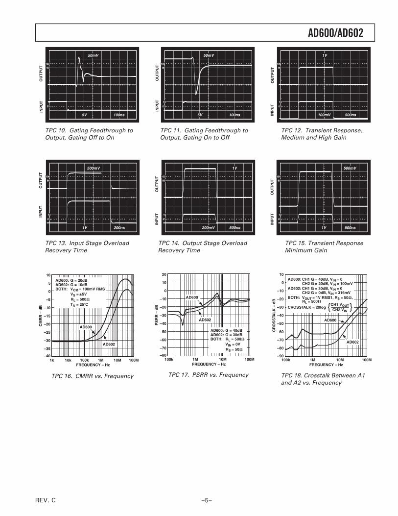
TPC 10. Gating Feedthrough toOutput, Gating Off to On
10
0%
100
90
500mV
1V
OU
TP
UT
INP
UT
200ns
TPC 13. Input Stage OverloadRecovery Time
1k 10k 100k 1M 10M 100M
10
–15
–40
5
0
–5
–10
–20
–25
–30
–35
CM
RR
– d
B
FREQUENCY – Hz
AD600: G = 20dBAD602: G = 10dBBOTH: VCM = 100mV RMS VS = 5V RL = 500
TA = 25C
AD600
AD602
TPC 16. CMRR vs. Frequency
10
0%
100
90
50mV
5V
OU
TP
UT
INP
UT
100ns
TPC 11. Gating Feedthrough toOutput, Gating On to Off
10
0%
100
90
1V
200mV
OU
TP
UT
INP
UT
500ns
TPC 14. Output Stage OverloadRecovery Time
20
–30
–80
10
0
–10
–20
–40
–50
–60
–70
PS
RR
– d
B
AD600
AD602
100k 1M 100M10MFREQUENCY – Hz
AD600: G = 40dBAD602: G = 30dBBOTH: RL = 500
VIN = 0V RS = 50
TPC 17. PSRR vs. Frequency
10
0%
100
90
1V
100mV
OU
TP
UT
INP
UT
500ns
TPC 12. Transient Response,Medium and High Gain
10
0%
100
90
500mV
1V
OU
TP
UT
INP
UT
500ns
TPC 15. Transient ResponseMinimum Gain
–30
–80
10
0
–10
–20
–40
–50
–60
–70
CR
OS
STA
LK
– d
B
AD602
–90100k 1M 100M10M
FREQUENCY – Hz
AD600: CH1 G = 40dB, VIN = 0CH2 G = 20dB, VIN = 100mV
AD602: CH1 G = 30dB, VIN = 0CH2 G = 0dB, VIN = 316mV
BOTH: VOUT = 1V RMS1, RS = 50,RL = 500
CROSSTALK = 20logCH1 VOUTCH2 VIN
AD600
TPC 18. Crosstalk Between A1and A2 vs. Frequency

REV. C
AD600/AD602
–6–
THEORY OF OPERATIONThe AD600 and AD602 have the same general design andfeatures. They comprise two fixed gain amplifiers, each pre-ceded by a voltage-controlled attenuator of 0 dB to 42.14 dBwith independent control interfaces, each having a scaling factorof 32 dB per volt. The gain of each amplifier in the AD600 islaser trimmed to 41.07 dB (X113), providing a control rangeof –1.07 dB to 41.07 dB (0 dB to 40 dB with overlap), whilethe AD602 amplifiers have a gain of 31.07 dB (X35.8) andprovide an overall gain of –11.07 dB to 31.07 dB (–10 dB to+30 dB with overlap).
The advantage of this topology is that the amplifier can usenegative feedback to increase the accuracy of its gain. Also, sincethe amplifier never has to handle large signals at its input, thedistortion can be very low. Another feature of this approach isthat the small-signal gain and phase response, and thus thepulse response, are essentially independent of gain.
The following discussion describes the AD600. Figure 1 is asimplified schematic of one channel. The input attenuator is aseven-section R-2R ladder network, using untrimmed resistorsof nominally R = 62.5 Ω, which results in a characteristic resis-tance of 125 Ω ± 20%. A shunt resistor is included at the inputand laser trimmed to establish a more exact input resistance of100 Ω ± 2%, which ensures accurate operation (gain and HPcorner frequency) when used in conjunction with external resis-tors or capacitors.
PRECISION PASSIVEINPUT ATTENUATOR GATING
INTERFACESCALING
REFERENCE
GAT1
A1OP
A1CM
C1HI
C1LO
A1HI
A1LO
VG
R – 2R LADDER NETWORK
GAIN CONTROLINTERFACE
RF22.24k(AD600)694(AD602)
RF120
FIXED-GAINAMPLIFIER
41.07dB(AD600)31.07(AD602)
500
0dB
–6.02dB
–12.04dB
–18.06dB
–22.08dB
–30.1dB
–36.12dB
–42.14dB
62.5
Figure 1. Simplified Block Diagram of Single Channel ofthe AD600 and AD602
The nominal maximum signal at input A1HI is 1 V rms (±1.4 Vpeak) when using the recommended ± 5 V supplies, althoughoperation to ±2 V peak is permissible with some increase in HFdistortion and feedthrough. Each attenuator is provided with aseparate signal “LO” connection for use in rejecting common-mode, the voltage between input and output grounds. Circuitryis included to provide rejection of up to ±100 mV.
The signal applied at the input of the ladder network is attenu-ated by 6.02 dB by each section; thus, the attenuation to each ofthe taps is progressively 0, 6.02, 12.04, 18.06, 24.08, 30.1, 36.12,and 42.14 dB. A unique circuit technique is employed to interpo-late between these tap points, indicated by the “slider” in Figure1, providing continuous attenuation from 0 dB to 42.14 dB.
To understand the AD600, it will help to think in terms of amechanical means for moving this slider from left to right; infact, it is voltage controlled. The details of the control interfaceare discussed later. Note that the gain is exactly determinedat all times, and a linear decibel relationship is automaticallyguaranteed between the gain and the control parameter thatdetermines the position of the slider. In practice, the gaindeviates from the ideal law, by about ±0.2 dB peak (see Figure 6).
Note that the signal inputs are not fully differential. A1LO,A1CM (for CH1), A2LO, and A2CM (for CH2) provideseparate access to the input and output grounds. This recog-nizes that even when using a ground plane, small differenceswill arise in the voltages at these nodes. It is important thatA1LO and A2LO be connected directly to the input ground(s).Significant impedance in these connections will reduce the gainaccuracy. A1CM and A2CM should be connected to the loadground(s).
Noise PerformanceAn important reason for using this approach is the superiornoise performance that can be achieved. The nominal resistanceseen at the inner tap points of the attenuator is 41.7 Ω (one thirdof 125 Ω), which exhibits a Johnson noise spectral density (NSD)of 0.84 nV/√Hz (that is, √4kTR) at 27°C, which is a large fractionof the total input noise. The first stage of the amplifier contrib-utes another 1.12 nV/√Hz, for a total input noise of 1.4 nV/√Hz.
The noise at the 0 dB tap depends on whether the input isshort-circuited or open-circuited. When shorted, the minimumNSD of 1.12 nV/√Hz is achieved. When open, the resistanceof 100 Ω at the first tap generates 1.29 nV/√Hz, so the noiseincreases to a total of 1.71 nV/√Hz. This last calculation wouldbe important if the AD600 were preceded, for example, by a900 Ω resistor to allow operation from inputs up to ±10 V rms.However, in most cases the low impedance of the source willlimit the maximum noise resistance.
It will be apparent from the foregoing that it is essential to use alow resistance in the design of the ladder network to achieve lownoise. In some applications this may be inconvenient, requiringthe use of an external buffer or preamplifier. However, very fewamplifiers combine the needed low noise with low distortion atmaximum input levels, and the power consumption required toachieve this performance is quite high (due to the need to maintainvery low resistance values while also coping with large inputs).On the other hand, there is little value in providing a bufferwith high input impedance, since the usual reason for this—the minimization of loading of a high resistance source—is notcompatible with low noise.
Apart from the small variations just mentioned, the signal-to-noise (S/N) ratio at the output is essentially independent of theattenuator setting, since the maximum undistorted output is 1 Vrms and the NSD at the output of the AD600 is fixed at 113times 1.4 nV/√Hz, or 158 nV/√Hz. Thus, in a 1 MHz bandwidth,the output S/N ratio would be 76 dB. The input NSD of theAD600 and AD602 are the same, but because of the 10 dBlower gain in the AD602’s fixed amplifier, its output S/N ratio is10 dB better, or 86 dB in a 1 MHz bandwidth.

REV. C
AD600/AD602
–7–
The Gain-Control InterfaceThe attenuation is controlled through a differential, high imped-ance (15 MΩ) input, with a scaling factor that is laser trimmed to32 dB per volt, that is, 31.25 mV/dB. Each of the two amplifiershas its own control interface. An internal bandgap referenceensures stability of the scaling with respect to supply and tempera-ture variations, and is the only circuitry common to both channels.
When the differential input voltage VG = 0 V, the attenuator“slider” is centered, providing an attenuation of 21.07 dB,resulting in an overall gain of 20 dB (= –21.07 dB + 41.07 dB).When the control input is –625 mV, the gain is lowered by20 dB (= 0.625 × 32), to 0 dB; when set to 625 mV, the gain isincreased by 20 dB, to 40 dB. When this interface is over-driven in either direction, the gain approaches either –1.07 dB(= –42.14 dB + 41.07 dB) or 41.07 dB (= 0 + 41.07 dB),respectively.
The gain of the AD600 can be calculated using the followingsimple expression:
Gain (dB) = 32 VG + 20 (1)
where VG is in volts. For the AD602, the expression is:
Gain (dB) = 32 VG + 10 (2)
Operation is specified for VG in the range from –625 mV dcto +625 mV dc. The high impedance gain-control input ensuresminimal loading when driving many amplifiers in multiple-channelapplications. The differential input configuration provides flexibil-ity in choosing the appropriate signal levels and polarities forvarious control schemes.
For example, the gain-control input can be fed differentially tothe inputs, or single-ended by simply grounding the unusedinput. In another example, if the gain is to be controlled by aDAC providing a positive only ground referenced output, the“Gain Control LO” pin (either C1LO or C2LO) should bebiased to a fixed offset of 625 mV, to set the gain to 0 dBwhen “Gain Control HI” (C1HI or C2HI) is at zero, and to40 dB when at 1.25 V.
It is a simple matter to include a voltage divider to achieve otherscaling factors. When using an 8-bit DAC having a FS output of2.55 V (10 mV/bit), a divider ratio of 1.6 (generating 6.25 mV/bit) would result in a gain setting resolution of 0.2 dB/ bit. Later,we will discuss how the two sections of an AD600 or AD602may be cascaded, when various options exist for gain control.
Signal-Gating InputsEach amplifier section of the AD600 and AD602 is equippedwith a signal gating function, controlled by a TTL or CMOSlogic input (GAT1 or GAT2). The ground references for theseinputs are the signal input grounds A1LO and A2LO, respec-tively. Operation of the channel is unaffected when this input isLO or left open-circuited. Signal transmission is blocked whenthis input is HI. The dc output level of the channel is set towithin a few millivolts of the output ground (A1CM or A2CM),and simultaneously the noise level drops significantly. Thereduction in noise and spurious signal feedthrough is usefulin ultrasound beam-forming applications, where many amplifieroutputs are summed.
Common-Mode RejectionA special circuit technique provides rejection of voltages appear-ing between input grounds (A1LO and A2LO) and outputgrounds (A1CM and A2CM). This is necessary because of the“op amp” form of the amplifier, as shown in Figure 1. Thefeedback voltage is developed across the resistor RF1 (which, toachieve low noise, has a value of only 20 Ω). The voltagedeveloped across this resistor is referenced to the input common,so the output voltage is also referred to that node.
For zero differential signal input between A1HI and A1LO,the output A1OP simply follows the voltage at A1CM. Note thatthe range of voltage differences which can exist between A1LOand A1CM (or A2LO and A2CM) is limited to about ±100 mV.TPC 16 shows typical common-mode rejection ratio versusfrequency.
ACHIEVING 80 dB GAIN RANGEThe two amplifier sections of the X-AMP can be connectedin series to achieve higher gain. In this mode, the output ofA1 (A1OP and A1CM) drives the input of A2 via a high-passnetwork (usually just a capacitor) that rejects the dc offset. Thenominal gain range is now –2 dB to +82 dB for the AD600 or–22 dB to +62 dB for the AD602.
There are several options in connecting the gain-control inputs.The choice depends on the desired signal-to-noise ratio (SNR)and gain error (output ripple). The following examples featurethe AD600; the arguments generally apply to the AD602, withappropriate changes to the gain values.
Sequential Mode (Maximum S/N Ratio)In the sequential mode of operation, the SNR is maintained atits highest level for as much of the gain control range possible,as shown in Figure 2. Note here that the gain range is 0 dB to80 dB. Figure 3 shows the general connections to accomplishthis. Both gain-control inputs, C1HI and C2HI, are driven inparallel by a positive only, ground referenced source with arange of 0 V to 2.5 V.
VG
S/N
RAT
IO –
dB
85
303.0
45
35
0.0
40
–0.5
60
50
55
65
70
75
80
2.52.01.51.00.5
Figure 2. S/N Ratio vs. Control Voltage Sequential Control(1 MHz Bandwidth)
An auxiliary amplifier that senses the voltage differencebetween input and output commons is provided to rejectthis common voltage.

REV. C
AD600/AD602
–8–
The gains are offset (Figure 4) such that A2’s gain is increasedonly after A1’s gain has reached its maximum value. Note thatfor a differential input of –700 mV or less, the gain of a singleamplifier (A1 or A2) will be at its minimum value of –1.07 dB;for a differential input of +700 mV or more, the gain will be atits maximum value of 41.07 dB. Control inputs beyond theselimits will not affect the gain and can be tolerated without dam-age or foldover in the response. See the Specifications section ofthis data sheet for more details on the allowable voltage range.The gain is now
Gain (dB) = 32 VC (3)
where VC is the applied control voltage.
+41.07dB
20dB
+1.07dB –0.56dB
–1.07dB
40.56dB +38.93dB
0.592 1.908
A1 A2
0 0.625 1.25 1.875 2.50 20 40 60 80–2.14 82.14
GAIN (dB)
*GAIN OFFSET OF 1.07dB, OR 33.44mV
*
*
VC (V)
Figure 4. Explanation of Offset Calibration forSequential Control
When VC is set to zero, VG1 = –0.592 V and the gain of A1 is1.07 dB (recall that the gain of each amplifier section is 0 dB forVG = 625 mV); meanwhile, VG2 = –1.908 V so the gain of A2is –1.07 dB. The overall gain is thus 0 dB (see Figure 3a).When VC = 1.25 V, VG1 = 1.25 V – 0.592 V = 0.658 V, whichsets the gain of A1 to 40.56 dB, while VG2 = 1.25 V – 1.908 V =–0.658 V, which sets A2’s gain at –0.56 dB. The overall gain isnow 40 dB (see Figure 3b). When VC = 2.5 V, the gain of A1 is41.07 dB and that of A2 is 38.93 dB, resulting in an overall gainof 80 dB (see Figure 3c). This mode of operation is furtherclarified by Figure 5, which is a plot of the separate gains of A1and A2 and the overall gain versus the control voltage. Figure 6is a plot of the gain error of the cascaded amplifiers versus thecontrol voltage.
Parallel Mode (Simplest Gain-Control Interface)In this mode, the gain-control voltage is applied to both inputsin parallel—C1HI and C2HI are connected to the control volt-age, and C1LO and C2LO are optionally connected to an offsetvoltage of 0.625 V. The gain scaling is then doubled to 64 dB/V,requiring only 1.25 V for an 80 dB change of gain. The ampli-tude of the gain ripple in this case is also doubled, as shown inFigure 7, and the instantaneous signal-to-noise ratio at theoutput of A2 decreases linearly as the gain is increased (Figure 8).
Low Ripple Mode (Minimum Gain Error)As can be seen in Figures 6 and 7, the output ripple is periodic.By offsetting the gains of A1 and A2 by half the period of theripple, or 3 dB, the residual gain errors of the two amplifierscan be made to cancel. Figure 9 shows the much lower gainripple when configured in this manner. Figure 10 plots theS/N ratio as a function of gain; it is very similar to that in the“Parallel Mode.”
VO2 = 1.908V
(a)
41.07dBINPUT0dB
VC = 0V
–40.00dB
–40.00dB
C1HI C1LO1.07dB
VG1 VG2VO1 = 0.592V
OUTPUT0dB41.07dB
–41.07dB
–42.14dB
C1HI C1LO
VC = 1.25V
–0.51dB
OUTPUT40dB
VC = 2.5V
38.93dB
OUTPUT80dB
A1
VO2 = 1.908V
(b)
41.07dBINPUT0dB
–0.51dB
C1HI C1LO
VG1 VG2VO1 = 0.592V
41.07dB
–1.07dB
–41.63dB
C1HI C1LO
VO2 = 1.908V
(c)
41.07dBINPUT0dB
0dB
0dB
C1HI C1LO
VG1 VG2VO1 = 0.592V
41.07dB–2.14dB
C1HI C1LO
40.56dB
41.07dB
A2
Figure 3. AD600 Gain Control Input Calculations for Sequential Control Operation

REV. C
AD600/AD602
–9–
90
–103.0
20
0
0.0
10
–0.5
50
30
40
60
70
80
2.52.01.51.00.5
COMBINED
VC
OV
ER
AL
L G
AIN
– d
B
A1
A2
Figure 5. Plot of Separate and Overall Gains inSequential Control
5
–83.0
–5
–7
0.0
–6
–0.5
–2
–4
–3
–1
1
2
4
3
0
2.0 2.51.51.00.5VC
GA
IN E
RR
OR
– d
B
Figure 6. Gain Error for Cascaded Stages —Sequential Control
5
–3
–5
0
–4
–0.1
0
–2
–1
1
2
3
4
1.21.00.80.40.2 0.6
GA
IN E
RR
OR
– d
B
VC
–6
Figure 7. Gain Error for Cascaded Stages —Parallel Control
75
301.4
40
35
0.20.0
45
50
55
60
65
70
1.21.00.80.60.4
S/N
RAT
IO –
dB
VC
Figure 8. SNR for Cascaded Stages — ParallelControl
1.2
–1.21.3
–0.6
–1.0
0.1
–0.8
0.0
0.0
–0.4
–0.2
0.2
0.4
0.6
1.0
0.8
1.21.11.00.90.70.60.50.40.30.2 0.8
GA
IN E
RR
OR
– d
B
VC
Figure 9. Gain Error for Cascaded Stages —Low Ripple Mode
80
351.4
45
40
0.20.0
50
55
60
65
70
75
1.21.00.80.60.4
VC
S/N
RAT
IO –
dB
Figure 10. ISNR vs. Control Voltage —Low Ripple Mode

REV. C
AD600/AD602
–10–
APPLICATIONSThe full potential of any high performance amplifier can only berealized by careful attention to details in its applications. Thefollowing pages describe fully tested circuits in which many suchdetails have already been considered. However, as is always trueof high accuracy, high speed analog circuits, the schematic isonly part of the story; this is no less true for the AD600 andAD602. Appropriate choices in the overall board layout and thetype and placement of power supply decoupling components arevery important. As explained previously, the input groundsA1LO and A2LO must use the shortest possible connections.
The following circuits show examples of time-gain control forultrasound and for sonar, methods for increasing the outputdrive, and AGC amplifiers for audio and RF/IF signal process-ing using both peak and rms detectors. These circuits alsoillustrate methods of cascading X-AMPs for either maintainingthe optimal S/N ratio or maximizing the accuracy of the gain-control voltage for use in signal measurement. These AGCcircuits may be modified for use as voltage-controlled amplifiersfor use in sonar and ultrasound applications by removing thedetector and substituting a DAC or other voltage source forsupplying the control voltage.
Time-Gain Control (TGC) and Time-Variable Gain (TVG)Ultrasound and sonar systems share a similar requirement: bothneed to provide an exponential increase in gain in response to alinear control voltage, that is, a gain control that is “linear indB.” Figure 11 shows the AD600/AD602 configured for a con-trol voltage ramp starting at –625 mV and ending at +625 mVfor a gain-control range of 40 dB. The polarity of the gain-controlvoltage may be reversed and the control voltage inputs C1HI andC1LO reversed to achieve the same effect. The gain-controlvoltage can be supplied by a voltage-output DAC such as theAD7242, which contains two complete DACs, operates from ±5 Vsupplies, has an internal reference of +3 V, and provides ±3 V ofoutput swing. As such, it is well-suited for use with the AD600/AD602, needing only a few resistors to scale the output volt-age of the DACs to the levels needed by the AD600/AD602.
CONTROL VOLTAGE,
+625mV
–625mV
A1GAIN
0dB 40dB
VG
1
2
3
4
5
6
7
8
16
15
14
13
12
11
10
9
REF
A1
A2
C1HI
A1CM
A1OP
VNEG
A2OP
A2CM
C2HI
C1LO
A1HI
A1LO
GAT1
A2LO
A2HI
C2LO
VOLTAGE-OUTPUTDAC
VG
AD600 or AD602
GAT2
+5V
–5V
+
–
+
–
VPOS
Figure 11. The Simplest Application of the X-AMP Is as aTGC or TVG Amplifier in Ultrasound or Sonar. Only the A1Connections Are Shown for Simplicity.
Increasing Output DriveThe AD600/AD602’s output stage has limited capability fornegative-load driving capability. For driving loads less than500 Ω, the load drive may be increased by approximately 5 mAby connecting a 1 kΩ pull-down resistor from the output to thenegative supply (Figure 12).
Driving Capacitive LoadsFor driving capacitive loads of greater than 5 pF, insert a 10 Ωresistor between the output and the load. This lowers the possi-bility of oscillation.
VPOS
VNEG
VIN
1k
1
2
3
4
5
6
7
8
16
15
14
13
12
11
10
9
REF
A1
A2
C1HI
A1CM
A1OP
A2OP
A2CM
C2HI
C1LO
A1HI
A1LO
GAT1
A2LO
A2HI
C2LO
GAIN-CONTROLVOLTAGE
GAT2
+5V
–5V
+
–
+
–
AD600/AD602
ADDEDPULL-DOWNRESISTOR
Figure 12. Adding a 1 kΩ Pull-Down Resistor Increases theX-AMP’s Output Drive by About 5 mA. Only the A1 Con-nections Are Shown for Simplicity.
Realizing Other Gain RangesLarger gain ranges can be accommodated by cascading amplifi-ers. Combinations built by cascading two amplifiers include–20 dB to +60 dB (using one AD602), –10 dB to +70 dB (1/2of an AD602 followed by 1/2 of an AD600), and 0 dB to 80 dB(one AD600). In multiple-channel applications, extra protectionagainst oscillation can be provided by using amplifier sectionsfrom different packages.
An Ultralow Noise VCAThe two channels of the AD600 or AD602 can operate inparallel to achieve a 3 dB improvement in noise level, providing1 nV/√Hz without any loss of gain accuracy or bandwidth.
In the simplest case, as shown in Figure 13, the signal inputsA1HI and A2HI are tied directly together. The outputs A1OPand A2OP are summed via R1 and R2 (100 Ω each), and thecontrol inputs C1HI/C2HI and C1LO/C2LO operate in parallel.Using these connections, both the input and output resistancesare 50 Ω. Thus, when driven from a 50 Ω source and termi-nated in a 50 Ω load, the gain is reduced by 12 dB, so the gainrange becomes –12 dB to +28 dB for the AD600 and –22 dB to+18 dB for the AD602. The peak input capability remains unaf-fected (1 V rms at the IC pins, or 2 V rms from an unloaded50 Ω source). The loading on each output, with a 50 Ω load, iseffectively 200 Ω, because the load current is shared betweenthe two channels, so the overall amplifier still meets its specifiedmaximum output and distortion levels for a 200 Ω load. This ampli-fier can deliver a maximum sine wave power of 10 dBm to the load.

REV. C
AD600/AD602
–11–
An inexpensive circuit using complementary transistor typeschosen for their low rbb, is shown in Figure 14. The gain isdetermined by the ratio of the net collector load resistance tothe net emitter resistance. It is an open-loop amplifier. The gainwill be X2 (6 dB) only into a 100 Ω load, assumed to be pro-vided by the input resistance of the X-AMP; R2 and R7 are inshunt with this load, and their value is important in defining thegain. For small-signal inputs, both transistors contribute anequal transconductance that is rendered less sensitive to signallevel by the emitter resistors R4 and R5. They also play a domi-nant role in setting the gain.
This is a Class AB amplifier. As VIN increases in a positive direc-tion, Q1 conducts more heavily and its re becomes lower whileQ2 increases. Conversely, increasingly negative values of VIN
result in the re of Q2 decreasing, while the re of Q1 increases.The design is chosen such that the net emitter resistance isessentially independent of the instantaneous value of VIN, result-ing in moderately low distortion. Low values of resistance andmoderately high bias currents are important in achieving the lownoise, wide bandwidth, and low distortion of this preamplifier.Heavy decoupling prevents noise on the power supply lines frombeing conveyed to the input of the X-AMP.
Table I. Measured Preamplifier Performance
Measurement Value Unit
Gain (f = 30 MHz) 6 dBBandwidth (–3 dB) 250 MHzInput Signal for
1 dB Compression 1 V p-pDistortion
VIN = 200 mV p-p HD2 0.27 %HD3 0.14 %
VIN = 500 mV p-p HD2 0.44 %HD3 0.58 %
System Input Noise 1.03 nV/√HzSpectral Density (NSD)(Preamp plus X-AMP)
Input Resistance 1.4 kΩInput Capacitance 15 pFInput Bias Current ±150 µAPower Supply Voltage ±5 VQuiescent Current 15 mA
A Low Noise AGC Amplifier with 80 dB Gain RangeFigure 15 provides an example of the ease with which the AD600can be connected as an AGC amplifier. A1 and A2 are cascaded,with 6 dB of attenuation introduced by the 100 Ω resistor R1,while a time constant of 5 ns is formed by C1 and the 50 Ω ofnet resistance at the input of A2. This has the dual effect of (a)lowering the overall gain range from 0 dB–80 dB to 6 dB–74 dBand (b) introducing a single-pole low-pass filter with a–3 dB frequency of about 32 MHz. This ensures stability at themaximum gain for a slight reduction in the overall bandwidth.The capacitor C4 blocks the small dc offset voltage at the out-put of A1 (which might otherwise saturate A2 at its maximumgain) and introduces a high pass corner at about 8 kHz, usefulin eliminating low frequency noise and spurious signals whichmay be present at the input.
VPOS
VNEG
100
100
50
GAIN-CONTROLVOLTAGE
VG– +
VIN
VOUT
1
2
3
4
5
6
7
8
16
15
14
13
12
11
10
9
REF
A1
A2
AD600 or AD602
+
–
+
–
C1HI
A1CM
A1OP
A2OP
A2CM
C2HI
C1LO
A1HI
A1LO
GAT1
A2LO
A2HI
C2LO
GAT2
+5V
–5V
Figure 13. An Ultralow Noise VCA Using the AD600 orAD602
A Low Noise, 6 dB PreamplifierIn some ultrasound applications, a high input impedance pre-amplifier is needed to avoid the signal attenuation that resultsfrom loading the transducer by the 100 Ω input resistance of theX-AMP. High gain cannot be tolerated, because the peak trans-ducer signal is typically ±0.5 V, while the peak input capabilityof the AD600 or AD602 is only slightly more than ±1 V. Again of two is a suitable choice. It can be shown that if thepreamplifier’s overall referred-to-input (RTI) noise is to bethe same as that due to the X-AMP alone (1.4 nV/√Hz), thenthe input noise of a nX2 preamplifier must be √(3/4) times aslarge, that is, 1.2 nV/√Hz.
+5V
–5V
+5V
–5V
1F
1F
0.1F
0.1F
1F
1F
VIN INPUTGROUND
OUTPUTGROUND
R149.9
R2174
R442.2
R542.2
R3562
R6562
R7174
R849.9
Q1MRF904
Q2MM4049
100RIN OF X AMP
Figure 14. A Low Noise Preamplifier for the AD600 andAD602

REV. C
AD600/AD602
–12–
A simple half-wave detector is used, based on Q1 and R2. Theaverage current into capacitor C2 is just the difference betweenthe current provided by the AD590 (300 µA at 300 K, 27°C)and the collector current of Q1. In turn, the control voltage VG
is the time integral of this error current. When VG (thus the gain)is stable, the rectified current in Q1 must, on average, exactlybalance the current in the AD590. If the output of A2 is toosmall to do this, VG will ramp up, causing the gain to increase,until Q1 conducts sufficiently. The operation of this controlsystem will now be described in detail.
First, consider the particular case where R2 is zero and the out-put voltage VOUT is a square wave at, say, 100 kHz, well abovethe corner frequency of the control loop. During the time VOUT
is negative, Q1 conducts. When VOUT is positive, it is cut off.Since the average collector current is forced to be 300 µA and thesquare wave has a 50% duty-cycle, the current when conductingmust be 600 µA. With R2 omitted, the peak value of VOUT
would be just the VBE of Q1 at 600 µA (typically about 700 mV)or 2 VBE peak-to-peak. This voltage, hence the amplitude at whichthe output stabilizes, has a strong negative temperature coefficient(TC), typically –1.7 mV/°C. While this may not be troublesomein some applications, the correct value of R2 will render theoutput stable with temperature.
To understand this, first note that the current in the AD590 isclosely proportional to absolute temperature (PTAT). In fact,this IC is intended for use as a thermometer. For the moment,assume that the signal is a square wave. When Q1 is conducting,VOUT is the now the sum of VBE and a voltage that is PTAT andthat can be chosen to have an equal but opposite TC to that ofthe base-to-emitter voltage. This is actually nothing more thanthe “bandgap voltage reference” principle in thinly veiled disguise!When we choose R2 so that the sum of the voltage across itand the VBE of Q1 is close to the bandgap voltage of about1.2 V, VOUT will be stable over a wide range of temperatures,provided, that Q1 and the AD590 share the same thermalenvironment.
Since the average emitter current is 600 µA during each half-cycleof the square wave, a resistor of 833 Ω would add a PTAT volt-age of 500 mV at 300 K, increasing by 1.66 mV/°C. In practice,
the optimum value of R2 will depend on the transistor used and,to a lesser extent, on the waveform for which the temperaturestability is to be optimized; for the devices shown and sine wavesignals, the recommended value is 806 Ω. This resistor alsoserves to lower the peak current in Q1 and the 200 Hz LPfilter it forms with C2 helps to minimize distortion due to ripplein VG. Note that the output amplitude under sine wave condi-tions will be higher than for a square wave, since the averagevalue of the current for an ideal rectifier would be 0.637 times aslarge, causing the output amplitude to be 1.88 (= 1.2/0.637) V, or1.33 V rms. In practice, the somewhat nonideal rectifier resultsin the sine wave output being regulated to about 1.275 V rms.
An offset of 375 mV is applied to the inverting gain-controlinputs C1LO and C2LO. Thus the nominal –625 mV to +625 mVrange for VG is translated upwards (at VG´) to –0.25 V for mini-mum gain to 1 V for maximum gain. This prevents Q1 fromgoing into heavy saturation at low gains and leaves sufficient“headroom” of 4 V for the AD590 to operate correctly at highgains when using a 5 V supply.
In fact, the 6 dB interstage attenuator means that the overallgain of this AGC system actually runs from –6 dB to +74 dB.Thus, an input of 2 V rms would be required to produce a 1 Vrms output at the minimum gain, which exceeds the 1 V rmsmaximum input specification of the AD600. The available gainrange is therefore 0 dB to 74 dB (or, X1 to X5000). Since thegain scaling is 15.625 mV/dB (because of the cascaded stages)the minimum value of VG´ is actually increased by 6 × 15.625 mV,or about 94 mV, to –156 mV, so the risk of saturation in Q1is reduced.
The emitter circuit of Q1 is somewhat inductive (due its finite ftand base resistance). Consequently, the effective value of R2increases with frequency. This would result in an increase in thestabilized output amplitude at high frequencies, but for the addi-tion of C3, determined experimentally to be 15 pF for the 2N3904for maximum response flatness. Alternatively, a faster transistorcan be used here to reduce HF peaking. Figure 16 shows the acresponse at the stabilized output level of about 1.3 V rms. Fig-ure 17 demonstrates the output stabilization for sine waveinputs of 1 mV to 1 V rms at frequencies of 100 kHz, 1 MHz,and 10 MHz.
1
2
3
4
5
6
7
8
16
15
14
13
12
11
10
9
REF
A1
A2
+
–
+
–
AD600
C1HI
A1CM
A1OP
VPOS
VNEG
A2OP
A2CM
C2HI
C1LO
A1HI
A1LO
GAT1
GAT2
A2LO
A2HI
C2LO
R1100
RFINPUT
C40.1F
C1100pF
5V
R346.4k
R43.74k
C315pF
C21F
R2806
1%
AD590
5V
300A(at 300K)
Q12N3904
FB
FB
+5V
–5V
+5V DEC
–5V DEC
0.1F
0.1F
POWER SUPPLYDECOUPLING NETWORK
RFOUTPUT
+5V DEC
–5V DEC+
–VPTAT
VG
Figure 15. This Accurate HF AGC Amplifier Uses Just Three Active Components

REV. C
AD600/AD602
–13–
FREQUENCY – MHz
AG
C O
UT
PU
T C
HA
NG
E –
dB
1 10010
3dB
0.1
Figure 16. AC Response at the Stabilized Output Levelof 1.3 V RMS
0.001 0.01 10.1INPUT AMPLITUDE – V RMS
RE
LAT
IVE
OU
TP
UT
– d
B
–0.4
+0.2
–0.2
0100kHz
1MHz
10MHz
Figure 17. Output Stabilization vs. RMS Input forSine Wave Inputs at 100 kHz, 1 MHz, and 10 MHz
While the “bandgap” principle used here sets the output ampli-tude to 1.2 V (for the square wave case), the stabilization pointcan be set to any higher amplitude, up to the maximum outputof ± (VS – 2) V that the AD600 can support. It is only necessaryto split R2 into two components of appropriate ratio whoseparallel sum remains close to the zero-TC value of 806 Ω. Thisis illustrated in Figure 18, which shows how the output can beraised, without altering the temperature stability.
R2AC3
15pF
Q12N3904
VPTAT
RFOUTPUT
R2B
R2 = R2A R2B ≈ 806
TO AD600 PIN 16
TO AD600 PIN 11
+
–
AD590
5V
300A(at 300K)
C21F
Figure 18. Modification in Detector to Raise Output to2 V RMS
A Wide Range, RMS-Linear dB Measurement System(2 MHz AGC Amplifier with RMS Detector)Monolithic rms-dc converters provide an inexpensive means tomeasure the rms value of a signal of arbitrary waveform, andthey also may provide a low accuracy logarithmic (“decibel-scaled”) output. However, they have certain shortcomings. Thefirst of these is their restricted dynamic range, typically only50 dB. More troublesome is that the bandwidth is roughly pro-portional to the signal level; for example, the AD636 provides a3 dB bandwidth of 900 kHz for an input of 100 mV rms, buthas a bandwidth of only 100 kHz for a 10 mV rms input. Itslogarithmic output is unbuffered, uncalibrated and not stableover temperature. Considerable support circuitry, including atleast two adjustments and a special high TC resistor, is requiredto provide a useful output.
All of these problems can be eliminated using an AD636 asthe detector element in an AGC loop, in which the differencebetween the rms output of the amplifier and a fixed dc refer-ence are nulled in a loop integrator. The dynamic range andthe accuracy with which the signal can be determined are nowentirely dependent on the amplifier used in the AGC system. Sincethe input to the rms-dc converter is forced to a constant ampli-tude, close to its maximum input capability, the bandwidth is nolonger signal dependent. If the amplifier has an exactly exponen-tial (“linear-dB”) gain-control law, its control voltage VG isforced by the AGC loop to be have the general form:
V V
VVOUT SCALEIN RMS
REF= log ( )10 (4)
Figure 19 shows a practical wide dynamic range rms-respondingmeasurement system using the AD600. Note that the signaloutput of this system is available at A2OP, and the circuit canbe used as a wideband AGC amplifier with an rms-respondingdetector. This circuit can handle inputs from 100 µV to 1 V rmswith a constant measurement bandwidth of 20 Hz to 2 MHz,limited primarily by the AD636 rms converter. Its logarithmicoutput is a loadable voltage accurately calibrated to 100 mV/dB,or 2 V per decade, which simplifies the interpretation of thereading when using a DVM and is arranged to be –4 V for aninput of 100 µV rms input, zero for 10 mV, and +4 V for a1 V rms input. In terms of Equation 4, VREF is 10 mV andVSCALE is 2 V.
Note that the peak “log output” of ± 4 V requires the use of±6 V supplies for the dual op amp U3 (AD712) although lowersupplies would suffice for the AD600 and AD636. If only ±5 Vsupplies are available, it will be either necessary to use a reducedvalue for VSCALE (say 1 V, in which case the peak output wouldbe only ± 2 V) or restrict the dynamic range of the signal toabout 60 dB.
As in the previous case, the two amplifiers of the AD600 areused in cascade. However, the 6 dB attenuator and low-passfilter found in Figure 1 are replaced by a unity gain bufferamplifier U3A, whose 4 MHz bandwidth eliminates the risk ofinstability at the highest gains. The buffer also allows the use ofa high impedance coupling network (C1/R3) that introduces ahigh-pass corner at about 12 Hz. An input attenuator of 10 dB(X0.316) is now provided by R1 + R2 operating in conjunctionwith the AD600’s input resistance of 100 Ω. The adjustmentprovides exact calibration of the logarithmic intercept VREF incritical applications, but R1 and R2 may be replaced by a fixed

REV. C
AD600/AD602
–14–
resistor of 215 Ω if very close calibration is not needed, since theinput resistance of the AD600 (and all other key parameters of itand the AD636) are already laser trimmed for accurate operation.This attenuator allows inputs as large as ±4 V to be accepted,that is, signals with an rms value of 1 V combined with a crestfactor of up to 4.
The output of A2 is ac coupled via another 12 Hz high-passfilter formed by C2 and the 6.7 kΩ input resistance of theAD636. The averaging time constant for the rms-dc converter isdetermined by C4. The unbuffered output of the AD636 (at Pin8) is compared with a fixed voltage of 316 mV set by the posi-tive supply voltage of 6 V and resistors R6 and R7. VREF isproportional to this voltage, and systems requiring greater cali-bration accuracy should replace the supply dependent referencewith a more stable source.
Any difference in these voltages is integrated by the op ampU3B, with a time constant of 3 ms formed by the parallel sum ofR6/R7 and C3. Now, if the output of the AD600 is too high, Vrms will be greater than the “setpoint” of 316 mV, causing theoutput of U3B—that is, VOUT—to ramp up (note that the inte-grator is noninverting). A fraction of VOUT is connected to theinverting gain-control inputs of the AD600, so causing the gainto be reduced, as required, until V rms is exactly equal to 316 mV,at which time the ac voltage at the output of A2 is forced to beexactly 316 mV rms. This fraction is set by R4 and R5 suchthat a 15.625 mV change in the control voltages of A1 andA2—which would change the gain of the cascaded amplifiers by1 dB—requires a change of 100 mV at VOUT. Notice here thatsince A2 is forced to operate at an output level well below itscapacity, waveforms of high crest factor can be tolerated through-out the amplifier.
To check the operation, assume an input of 10 mV rms isapplied to the input, which results in a voltage of 3.16 mV rmsat the input to A1, due to the 10 dB loss in the attenuator. If thesystem operates as claimed, VOUT (and hence VG) should bezero. This being the case, the gain of both A1 and A2 will be20 dB and the output of the AD600 will therefore be 100 times(40 dB) greater than its input, which evaluates to 316 mV rms,
the input required at the AD636 to balance the loop. Finally,note that unlike most AGC circuits, needing strong temperaturecompensation for the internal “kT/q” scaling, these voltages,and thus the output of this measurement system, are tempera-ture stable, arising directly from the fundamental and exactexponential attenuation of the ladder networks in the AD600.
Typical results are presented for a sine wave input at 100 kHz.Figure 20 shows that the output is held very close to the set-point of 316 mV rms over an input range in excess of 80 dB.
450
300
15010V 100V 10V1V100mV10mV1mV
225
375
350
200
275
425
325
175
250
400
INPUT SIGNAL – V RMS
VO
UT –
mV
Figure 20. The RMS Output of A2 Is Held Close to the“Setpoint” 316 mV for an Input Range of Over 80 dB
This system can, of course, be used as an AGC amplifier, inwhich the rms value of the input is leveled. Figure 21 showsthe “decibel” output voltage. More revealing is Figure 22, whichshows that the deviation from the ideal output predicted byEquation 1 over the input range 80 µV to 500 mV rms is within±0.5 dB, and within ±1 dB for the 80 dB range from 80 µV to800 mV. By suitable choice of the input attenuator R1 + R2,this could be centered to cover any range from 25 mV to 250 mVto, say, 1 mV to 10 V, with appropriate correction to the valueof VREF. Note that VSCALE is not affected by the changes in the
C1HI
A1CM
A1OP
VPOS
VNEG
A2OP
A2CM
C2HI
C1LO
A1HI
A1LO
GAT1
GAT2
A2LO
A2HI
C2LO
1
2
3
4
5
6
7
14
13
12
11
10
9
8
U2AD636
VINP
VNEG
CAVG
VLOG
BFOP
BFIN
VPOS
COMM
LDLO
VRMS
INPUT1V RMS
MAX(SINE WAVE)
R1115
R2 200
R3133k
U3A
1/2AD712
R43.01k
R516.2k
VG15.625mV/dB
C10.1F
C22F
NC
NC
NC
NC
NC
NC
VRMS
AF/RFOUTPUT C4
4.7F+6V DEC
R756.2k
R63.16k
C31F
U3B1/2AD712
+316.2mV
VOUT+100mV/dB0V = 0dB(AT 10mV RMS)
NC = NO CONNECT
1
2
3
4
5
6
7
8
16
15
14
13
12
11
10
9
REF
A1
A2
+
–
+
–
U1 AD600
FB
FB
+6V
–6V
+6VDEC
–6VDEC
0.1F
0.1F
POWER SUPPLYDECOUPLING
NETWORK
CAL0dB
+6VDEC
–6VDEC
–6VDEC
Figure 19. The Output of This Three-IC Circuit Is Proportional to the Decibel Value of the RMS Input

REV. C
AD600/AD602
–15–
range. The gain ripple of ±0.2 dB seen in this curve is the result ofthe finite interpolation error of the X-AMP. Note that it occurswith a periodicity of 12 dB—twice the separation between thetap points (because of the two cascaded stages).
5
0
–5
1
2
3
4
–4
–3
–2
–1VO
UT
– V
olt
s
10V 100V 10V1V100mV10mV1mVINPUT SIGNAL – V RMS
Figure 21. The dB Output of Figure 19’s Circuit Is LinearOver an 80 dB Range
2.5
0
–2.5
0.5
1.0
1.5
2.0
–2.0
–1.5
–1.0
–0.5
OU
TP
UT
ER
RO
R –
dB
10V 100V 10V1V100mV10mV1mVINPUT SIGNAL – V RMS
Figure 22. Data from Figure 20 Presented as the Deviationfrom the Ideal Output Given in Equation 4
This ripple can be canceled whenever the X-AMP stages arecascaded by introducing a 3 dB offset between the two pairsof control voltages. A simple means to achieve this is shownin Figure 23: the voltages at C1HI and C2HI are “split” by±46.875 mV, or ±1.5 dB. Alternatively, either one of these pinscan be individually offset by 3 dB and a 1.5 dB gain adjustmentmade at the input attenuator (R1 + R2).
16
15
14
13
12
11
10
9
U1AD600
C1HI
A1CM
A1OPVPOS
VNEG
A2OP
A2CM
C2HI
+6V DEC
–6V DEC C22F
1
2
3
4
5
6
7
VINP
VNEG
CAVG
VLOG
BFOP
BFIN
U2AD636
NC
NC
NC
–6V DEC
–46.875mV
NC = NO CONNECT
10k 10k
+6VDEC
–6VDEC 78.7 78.7
3dB OFFSETMODIFICATION
+46.875mV
Figure 23. Reducing the Gain Error Ripple
The error curve shown in Figure 24 demonstrates that over thecentral portion of the range the output voltage can be maintainedvery close to the ideal value. The penalty for this modification isthe higher errors at the extremities of the range. The next twoapplications show how three amplifier sections can be cascadedto extend the nominal conversion range to 120 dB, with theinclusion of simple LP filters of the type shown in Figure 15.Very low errors can then be maintained over a 100 dB range.
2.5
0
–2.5
0.5
1.0
1.5
2.0
–2.0
–1.5
–1.0
–0.5
OU
TP
UT
ER
RO
R –
dB
10V 100V 10V1V100mV10mV1mVINPUT SIGNAL – V RMS
Figure 24. Using the 3 dB Offset Network, the RippleIs Reduced
100 dB to 120 dB RMS Responding Constant Bandwidth AGCSystems with High Accuracy dB OutputsThe next two applications double as both AGC amplifiers andmeasurement systems. In both, precise gain offsets are used toachieve either (1) a very high gain linearity of ± 0.1 dB overthe full 100 dB range or (2) the optimal signal-to-noise ratioat any gain.

REV. C
AD600/AD602
–16–
A 100 dB RMS/AGC System with Minimal Gain Error(Parallel Gain with Offset)Figure 25 shows an rms-responding AGC circuit that canequally well be used as an accurate measurement system. Itaccepts inputs of 10 µV to 1 V rms (–100 dBV to 0 dBV) withgenerous overrange. Figure 26 shows the logarithmic output, VLOG,which is accurately scaled 1 V per decade, that is 50 mV/dB, withan intercept (VLOG = 0) at 3.16 mV rms (–50 dBV). Gain offsetsof ±2 dB have been introduced between the amplifiers, providedby the ±62.5 mV introduced by R6–R9. These offsets cancel asmall gain ripple which arises in the X-AMP from its finite interpo-lation error, which has a period of 18 dB in the individual VCAsections. The gain ripple of all three amplifier sections withoutthis offset (in which case the gain errors simply add) is shown inFigure 27; it is still a remarkably low ±0.25 dB over the 108 dBrange from 6 µV to 1.5 V rms. However, with the gain offsetsconnected, the gain linearity remains under ±0.1 dB over thespecified 100 dB range (Figure 28).
5
3
–51V 10V 10V1V100mV10mV1mV100V
4
2
0
1
–1
–3
–2
–4
INPUT SIGNAL – V RMS
LO
GA
RIT
HM
IC O
UT
PU
T –
V
Figure 26. VLOG Plotted vs. VIN for Figure 25‘s CircuitShowing 120 dB AGC Range
C1HI
A1CM
A1OP
VPOS
VNEG
A2OP
A2CM
C2HI
C1LO
A1HI
A1LO
GAT1
GAT2
A2LO
A2HI
C2LO
+5VDEC–5VDEC
–5VDEC
NC
NC
NC
NC
NC
NC
C522F
+5V DEC
R1146.4k
R103.16k
U3C
INPUT1V RMS
MAX(SINE WAVE) U3A
1/4AD713
C20.1F
NC = NO CONNECT
R610k
R7127
R8127
R910k
+5V–5V
C1HI
A1CM
A1OP
VPOS
VNEG
A2OP
A2CM
C2HI
C1LO
A1HI
A1LO
GAT1
GAT2
A2LO
A2HI
C2LO
C42F
C10.1F
C3220pF
R4133k
R51.58k
R2487
R3200R1
133k
–2dB–62.5mV 0dB
+2dB+62.5mV
C64.7F
+316.2mV
R166.65k
R1519.6k
+5V DEC
R133.01k
R1211.3k
R14301k
Q12N3906
1
2
3
4
5
6
7
14
13
12
11
10
9
8
U4AD636
VINP
VNEG
CAVG
VLOG
BFOP
BFIN
VPOS
COMM
LDLO
VRMS
FB
FB
+5V
–5V
+5VDEC
–5VDEC
0.1F
0.1F
POWER SUPPLYDECOUPLING
NETWORK
1
2
3
4
5
6
7
8
16
15
14
13
12
11
10
9
REF
A1
A2
+
–
+
–
U1 AD600
U3B
1/4AD713
1
2
3
4
5
6
7
8
16
15
14
13
12
11
10
9
REF
A1
A2
+
–
+
–
U2 AD600
VOUT
+5VDEC–5VDEC
1/4AD713
VLOG
Figure 25. RMS Responding AGC Circuit with 100 dB Dynamic Range

REV. C
AD600/AD602
–17–
2.0
–2.0
0.5
1.0
1.5
–1.5
–1.0
–0.5
GA
IN E
RR
OR
– d
B
–0.1
0.10
1V 10V 10V1V100mV10mV1mV100VINPUT SIGNAL – V RMS
Figure 27. Gain Error for Figure 19 Without the 2 dBOffset Modification
2.0
–2.0
0.5
1.0
1.5
–1.5
–1.0
–0.5
GA
IN E
RR
OR
– d
B
–0.1
0.10
1V 10V 10V1V100mV10mV1mV100VINPUT SIGNAL – V RMS
Figure 28. Adding the 2 dB Offsets Improves theLinearization
The maximum gain of this circuit is 120 dB. If no filtering wereused, the noise spectral density of the AD600 (1.4 nV/√Hz)would amount to an input noise of 8.28 µV rms in the full band-width (35 MHz). At a gain of one million, the output noisewould dominate. Consequently, some reduction of bandwidth ismandatory, and in the circuit of Figure 25 it is due mostly toa single-pole low-pass filter R5/C3, which provides a –3 dBfrequency of 458 kHz, which reduces the worst-case outputnoise (at VAGC) to about 100 mV rms at a gain of 100 dB. Ofcourse, the bandwidth (and hence output noise) could be easilyreduced further, for example, in audio applications, merely byincreasing C3. The value chosen for this application is optimalin minimizing the error in the VLOG output for small input signals.
The AD600 is dc-coupled, but even miniscule offset voltages atthe input would overload the output at high gains, so high-passfiltering is also needed. To provide operation at low frequencies,two simple zeros at about 12 Hz are provided by R1/C1 andR4/C2; op amp sections U3A and U3B (AD713) are used toprovide impedance buffering, since the input resistance of theAD600 is only 100 Ω. A further zero at 12 Hz is provided by C4and the 6.7 kΩ input resistance of the AD636 rms converter.
The rms value of VLOG is generated at Pin 8 of the AD636; theaveraging time for this process is determined by C5, and the
value shown results in less than 1% rms error at 20 Hz. Theslowly varying V rms is compared with a fixed reference of316 mV, derived from the positive supply by R10/R11. Anydifference between these two voltages is integrated in C6, inconjunction with op amp U3C, the output of which is VLOG. Afraction of this voltage, determined by R12 and R13, is returnedto the gain control inputs of all AD600 sections. An increase inVLOG lowers the gain, because this voltage is connected to theinverting polarity control inputs.
Now, in this case, the gains of all three VCA sections are beingvaried simultaneously, so the scaling is not 32 dB/V but 96 dB/V,or 10.42 mV/dB. The fraction of VLOG required to set its scalingto 50 mV/dB is therefore 10.42/50, or 0.208. The resulting full-scale range of VLOG is nominally ±2.5 V. This scaling allows thecircuit to operate from ±5 V supplies. Optionally, the scalingcan be altered to 100 mV/dB, which would be more easilyinterpreted when VLOG is displayed on a DVM, by increasingR12 to 25.5 kΩ. The full-scale output of ±5 V then requires theuse of supply voltages of at least ±7.5 V.
A simple attenuator of 16.6 ±1.25 dB is formed by R2/R3 andthe 100 Ω input resistance of the AD600. This allows the refer-ence level of the decibel output to be precisely set to zero for aninput of 3.16 mV rms, and thus center the 100 dB range between10 µV and 1 V. In many applications R2/R3 may be replacedby a fixed resistor of 590 Ω. For example, in AGC applica-tions, neither the slope nor the intercept of the logarithmic outputis important.
A few additional components (R14–R16 and Q1) improve theaccuracy of VLOG at the top end of the signal range (that is, forsmall gains). The gain starts rolling off when the input to thefirst amplifier, U1A, reaches 0 dB. To compensate for this non-linearity, Q1 turns on at VLOG ~ 1.5 V and increases the feedbackto the control inputs of the AD600s, thereby needing a smallervoltage at VLOG to maintain the input to the AD636 to the set-point of 316 mV rms.
A 120 dB RMS/AGC System with Optimal S/N Ratio(Sequential Gain)In the last case, all gains were adjusted simultaneously, resultingin an output signal-to-noise ratio (S/N ratio) which is always lessthan optimal. The use of sequential gain control results in amajor improvement in S/N ratio, with only a slight penalty inthe accuracy of VLOG, and no penalty in the stabilization accuracyof VAGC. The idea is to increase the gain of the earlier stagesfirst (as the signal level decreases) and maintain the highest S/Nratio throughout the amplifier chain. This can be easilyachieved with the AD600 because its gain is accurate even whenthe control input is overdriven. That is, each gain control“window” of 1.25 V is used fully before moving to the nextamplifier to the right.
Figure 29 shows the circuit for the sequential control scheme.R6 to R9 with R16 provide offsets of 42.14 dB between theindividual amplifiers to ensure smooth transitions between thegain of each successive X-AMP, with the sequence of gainincrease being U1A first, then U1B, and lastly U2A. The adjust-able attenuator provided by R3 + R17 and the 100 Ω inputresistance of U1A as well as the fixed 6 dB attenuation providedby R2 and the input resistance of U1B are included both to setVLOG to read 0 dB when VIN is 3.16 mV rms and to center the100 dB range between 10 µV rms and 1 V rms input. R5 andC3 provide a 3 dB noise bandwidth of 30 kHz. R12 to R15

REV. C
AD600/AD602
–18–
change the scaling from 625 mV/decade at the control inputs to1 V/decade at the output and at the same time center the dynamicrange at 60 dB, which occurs if the VG of U1B is equal to zero.These arrangements ensure that the VLOG will still fit within the±6 V supplies.
5
3
–5
4
2
0
1
–1
–3
–2
–4
LO
GA
RIT
HM
IC O
UT
PU
T –
V
1V 10V 10V1V100mV10mV1mV100V
INPUT SIGNAL – V RMS
Figure 30. VLOG Is Essentially Linear Over the Full 120 dBRange
Figure 30 shows VLOG to be linear over a full 120 dB range.Figure 31 shows the error ripple due to the individual gain func-tions which is bounded by ±0.2 dB (dotted lines) from 6 µV to 2 V.The small perturbations at about 200 µV and 20 mV, causedby the impracticality of matching the gain functions perfectly,are the only sign that the gains are now sequential. Figure 32 isa plot of VAGC that remains very close to its set value of 316 mVrms over the full 120 dB range.
To compare the signal-to-noise ratios in the “simultaneous”and “sequential” modes of operation more directly, all inter-stage attenuation was eliminated (R2 and R3 in Figure 25, R2in Figure 29), the input of U1A was shorted, R5 was selected toprovide a 20 kHz bandwidth (R5 = 7.87 kΩ), and only the gaincontrol was varied, using an external source. The rms value ofthe noise was then measured at VOUT and expressed as an S/Nratio relative to 0 dBV, this being almost the maximum outputcapability of the AD600. Results for the simultaneous mode canbe seen in Figure 33. The S/ N ratio degrades uniformly as thegain is increased. Note that since the inverting gain control wasused, the gain in this curve and in Figure 34 decreases for morepositive values of the gain-control voltage.
R147.32k
R155.11k
+6V DEC
R13866
R121k
C1HI
A1CM
A1OP
VPOS
VNEG
A2OP
A2CM
C2HI
C1LO
A1HI
A1LO
GAT1
GAT2
A2LO
A2HI
C2LO
+6VDEC–6VDEC
–6VDEC
NC
NC
NC
NC
NC
NC
C522F
+6V DEC
R1156.2k
R103.16k
U3C
U3A
1/4AD713
C20.1F
NC = NO CONNECT
R63.4k
R8294
+5V
C1HI
A1CM
A1OP
VPOS
VNEG
A2OP
A2CM
C2HI
C1LO
A1HI
A1LO
GAT1
GAT2
A2LO
A2HI
C2LO
C42F
C10.1F
C30.001F
R4133k
R55.36k
R2100
R1133k
C64.7F
+316.2mV
1
2
3
4
5
6
7
14
13
12
11
10
9
8
U4AD636
VINP
VNEG
CAVG
VLOG
BFOP
BFIN
VPOS
COMM
LDLO
VRMS
FB
FB
+6V
–6V
+6VDEC
–6VDEC
0.1F
0.1F
POWER SUPPLYDECOUPLING
NETWORK
U3B
1/4AD713
1
2
3
4
5
6
7
8
16
15
14
13
12
11
10
9
REF
A1
A2
+
–
+
–
U2 AD600
VOUT
+5VDEC–5VDEC
1/4AD713
VLOG
R71k
R16287
R91k
R17115
R3200
0dBADJUST
INPUT1
2
3
4
5
6
7
8
16
15
14
13
12
11
10
9
REF
A1
A2
+
–
+
–
U1 AD600
Figure 29. 120 dB Dynamic Range RMS Responding Circuit Optimized for S/N Ratio

REV. C
AD600/AD602
–19–
2.0
–2.0
0.5
1.0
1.5
–1.5
–1.0
–0.5
GA
IN E
RR
OR
– d
B
–0.2
0.20
1V 10V 10V1V100mV10mV1mV100VINPUT SIGNAL – V RMS
Figure 31. The Error Ripple Due to the Individual GainFunctions
400
300
200
350
250
GA
IN E
RR
OR
– m
V
1V 10V 10V1V100mV10mV1mV100VINPUT SIGNAL – V RMS
Figure 32. VAGC Remains Close to Its Setpoint of316 mV RMS Over the Full 120 dB Range
90
0833.2
20
10
–625.0–833.2
30
40
50
60
70
80
625.0416.6208.30–208.3–416.6CONTROL VOLTAGE, VC (10.417mV/dB) – mV
S/N
RAT
IO –
dB
Figure 33. S/N Ratio vs. Control Voltage for Parallel GainControl (Figure 25)
In contrast, the S/N ratio for the sequential mode is shown inFigure 34. U1A always acts as a fixed noise source; varying itsgain has no influence on the output noise. This is a feature ofthe X-AMP technique. Thus, for the first 40 dB of controlrange (actually slightly more, as explained below), when onlythis VCA section has its gain varied, the S/N ratio remains con-stant. During this time, the gains of U1B and U2A are at theirminimum value of –1.07 dB.
CONTROL VOLTAGE, VC (31.25mV/dB) – V
90
03.817
20
10
–0.558–1.183
30
40
50
60
70
80
3.1922.5671.9421.3170.6920.067
S/N
RAT
IO –
dB
Figure 34. S/N Ratio vs. Control Voltage for SequentialGain Control (Figure 29)
For the next 40 dB of control range, the gain of U1A remainsfixed at its maximum value of 41.07 dB and only the gain ofU1B is varied, while that of U2A remains at its minimum valueof –1.07 dB. In this interval, the fixed output noise of U1A isamplified by the increasing gain of U1B and the S/N ratio pro-gressively decreases.
Once U1B reaches its maximum gain of 41.07 dB, its outputalso becomes a gain independent noise source; this noise ispresented to U2A. As the control voltage is further increased,the gains of both U1A and U1B remain fixed at their maximumvalue of 41.07 dB, and the S/N ratio continues to decrease.Figure 34 clearly shows this, because the maximum S/N ratioof 90 dB is extended for the first 40 dB of input signal before itstarts to roll off.
This arrangement of staggered gains can be easily implementedbecause, when the control inputs of the AD600 are overdriven,the gain limits to its maximum or minimum values without sideeffects. This eliminates the need for awkward nonlinear shapingcircuits that have previously been used to break up the gainrange of multistage AGC amplifiers. It is the precise values of theAD600’s maximum and minimum gain (not 0 dB and 40 dBbut –1.07 dB and +41.07 dB) that explain the rather odd valuesof the offset values that are used.
The optimization of the output S/N ratio is of obvious value inAGC systems. However, in applications where these circuits areconsidered for their wide range logarithmic measurements capa-bilities, the inevitable degradation of the S/N ratio at high gainsneed not seriously impair their utility. In fact, the bandwidth ofthe circuit shown in Figure 25 was specifically chosen to improvemeasurement accuracy by altering the shape of the log error curve(Figure 31) at low signal levels.

–20–
C00
538–
0–5/
02(C
)P
RIN
TE
D IN
U.S
.A.
AD600/AD602
REV. C
PR
INT
ED
IN U
.S.A
.
OUTLINE DIMENSIONS
Dimensions shown in inches and (mm)
16-Lead Plastic DIP Package (N-16)
16
1 8
9
0.87 (22.1) MAX
0.25(6.35)
0.31(7.87)
0.035(0.89)
0.018(0.46)
0.18(4.57)
0.100(2.54)
0.033(0.84)
0.125(3.18)MIN
0.18 (4.57)MAX0.011(0.28)
7.62 (0.3)
Dimensions shown in inches and (mm)
16-Lead Cerdip Package(Q-16)
16
1 8
90.310 (7.87)0.220 (5.59)PIN 1
0.005 (0.13)MIN
0.840 (21.34) MAX
0.080 (2.03) MAX
15 0
0.320 (8.13)0.290 (7.37)
0.015 (0.38)0.008 (0.20)SEATING
PLANE
0.200 (5.08)MAX
0.150(3.81) MIN0.200 (5.08)
0.125 (3.18)0.023 (0.58)0.014 (0.36)
0.100(2.54)BSC
0.070 (1.78)0.030 (0.76)
0.060 (1.52)0.015 (0.38)
Dimensions shown in millimeters and (inches)
16-Lead SOIC Package(R-16)
10.50 (0.413)
1.27 (0.05)REF
16 9
81
10.65(0.419)
7.60(0.299)
0.30(0.012)
0.49(0.019)
2.65(0.104)
0.32(0.013)
0.75(0.030)
1.07(0.042)
CONTROLLING DIMENSIONS ARE IN MILLIMETERS; INCH DIMENSIONS (IN PARENTHESES) AREROUNDED-OFF MILLIMETER EQUIVALENTS FOR REFERENCE ONLY AND ARE NOT APPROPRIATEFOR USE IN DESIGN
Revision HistoryLocation Page
5/02–Data Sheet changed from REV. B to REV. C.
Changes to SPECIFICATIONS .................................................................................................................................................... 2
Renumber Tables and TPCs .................................................................................................................................................. Global
8/01–Data Sheet changed from REV. A to REV. B.
Changes to Accuracy Section of AD600A/AD602A column ............................................................................................................ 2
Changes to Ordering Guide ............................................................................................................................................................ 3
Changes to Figure 3 ....................................................................................................................................................................... 8