dual-channel,16-bit,800 msps, 2x– 8x … · dac5688 slls880c – december 2007– revised august...
TRANSCRIPT
DAC5688
www.ti.com SLLS880C –DECEMBER 2007–REVISED AUGUST 2010
DUAL-CHANNEL, 16-BIT, 800 MSPS, 2x–8x INTERPOLATINGDIGITAL-TO-ANALOG CONVERTER (DAC)
Check for Samples: DAC5688
1FEATURES DESCRIPTION• Dual, 16-Bit, 800 MSPS DACs The DAC5688 is a dual-channel 16-bit 800 MSPS
digital-to-analog converter (DAC) with dual CMOS• Dual, 16-Bit, 250 MSPS CMOS Input Datadigital data bus, integrated 2x-8x interpolation filters,– 16 Sample Input FIFOa fine frequency mixer with 32-bit complex
– Flexible input data bus options numerically controlled oscillator (NCO), on-board• High Performance clock multiplier, IQ compensation, and internal
voltage reference. Different modes of operation– 81 dBc ACLR WCDMA TM1 at 70 MHzenable or bypass various signal processing blocks.
• 2x-32x Clock Multiplying PLL/VCO The DAC5688 offers superior linearity, noise,• Selectable 2x–8x Interpolation Filters crosstalk and PLL phase noise performance.
– Stop-band Attenuation > 80 dB The DAC5688 dual CMOS data bus provides 250• Complex Mixer with 32-Bit NCO MSPS input data transfer per DAC channel. Several
input data options are available: dual-bus data,• Digital Quadrature Modulator Correctionsingle-bus interleaved data, even and odd
– Gain, Phase and Offset Correction multiplexing at half-rate, and an input FIFO with either• Digital Inverse SINC Filter external or internal clock to ease interface timing.
Input data can interpolated 2x, 4x or 8x by on-board• 3- or 4-Wire Serial Control Interfacedigital interpolating FIR filters with over 80 dB of
• On Chip 1.2-V Reference stop-band attenuation.• Differential Scalable Output: 2 to 20 mA
The DAC5688 allows both complex or real output. An• Package: 64-pin 9×9mm QFN optional 32-bit NCO/mixer in complex mode provides
frequency upconversion and the dual DAC outputAPPLICATIONS produces a complex Hilbert Transform pair. A digital
Inverse SINC filter compensates for natural DAC• Cellular Base Stationssin(x)/x frequency roll-off. The digital Quadrature• Broadband Wireless Access (BWA)Modulator Correction (QMC) feature allows IQ• WiMAX 802.16compensation of phase, gain and offset to maximize
• Fixed Wireless Backhaul sideband rejection and minimize LO feed-through of• Cable Modem Termination System (CMTS) an external quadrature modulator performing the final
single sideband RF up-conversion.
The DAC5688 is pin compatible with the DAC5689which does not include a clock-multiplying PLL. TheDAC5688 is characterized for operation over theindustrial temperature range of –40°C to 85°C and isavailable in a 64-pin 9x9mm QFN package.
ORDERING INFORMATION (1)
Order Code Package Qty PackageTA = –40°C to 85°C Tape and Reel Format Drawing/Type (2) (3)
DAC5688IRGCT 250RGC / 64QFN Quad Flatpack No-Lead
DAC5688IRGCR 2000
(1) For the most current package and ordering information, see the Package Option Addendum at the end of this document, or see the TIwebsite at www.ti.com.
(2) Thermal Pad Size: 7,4 mm × 7,4 mm(3) MSL Peak Temperature: Level-3-260C-168 HR
1
Please be aware that an important notice concerning availability, standard warranty, and use in critical applications of TexasInstruments semiconductor products and disclaimers thereto appears at the end of this data sheet.
PRODUCTION DATA information is current as of publication date. Copyright © 2007–2010, Texas Instruments IncorporatedProducts conform to specifications per the terms of the TexasInstruments standard warranty. Production processing does notnecessarily include testing of all parameters.

Internal Clock Generation and
2x - 32x PLL Clock Multiplier
CLK2
CLK2C
LPFCLKVDD DVDD
x2
x2
x2
x2
FIR1
AVDD
GND
RESETB
EXTIO
EXTLO
1.2 V
Reference
BIASJ
IOUTA1
IOUTA216-b DAC
2-8x Fdata
FIR4
IOUTB1
IOUTB2
16-b DAC
FIR3
xsin(x)
x
sin(x)
TXENABLE
DA[15:0]
DB[15:0]
CLKO_CLK1
LOCK_CLK1C
QMC
B-Offset
QMCA-Offset
B
gain
A
gain
SIF Control
SCLKSDENBSDOSDIO
Inp
ut
FIF
O/
Dem
ux
sin
32-bit NCO
cos
Fu
llM
ixe
r(F
MIX
)
Qu
ad
ratu
reM
od
ula
tor
Co
rrec
tio
n(Q
MC
):P
ha
se
&G
ainx2
x2
FIR2
2x – 8x Interpolation
SYNC
CLKOUT
LOCK
Updated: 2-Oct-07
IOVDD
67 taps 11 taps19 taps 9 taps
VFUSE
DA
7
DA
6
DA
5
DA
4
DA
3
DA
2
DA
1
DA
0
CL
KO
_CL
K1
LO
CK
_C
LK
1C
DB
0
DB
1
DB
2
DB
3
DB
4
DB
5
DB6
DB7
DB8
DB9
DB10
DB11
DVDD
DB12
DB13
DB14
DB15
VFUSE
SDO
SDIO
SCLK
SDENB
LP
F
DV
DD
AV
DD
AV
DD
IOU
TB
1
IOU
TB
2
EX
TLO
BIA
SJ
EX
TIO
AV
DD
IOU
TA
2
IOU
TA
1
AV
DD
AV
DD
DV
DD
RE
SE
TB
DA8
DA9
DA10
DA11
DA12
DA13
DVDD
DA14
DA15
IOVDD
SYNC
TXENABLE
GND
CLK2C
CLK2
CLKVDD
DAC5688
RGC Package64QFN, 9x9mm
(Top View)
49
50
51
52
53
54
55
56
57
58
59
60
61
62
63
64
1
2
3
4
5
6
7
8
9
10
11
12
13
14
15
16
32
31
30
29
28
27
26
25
24
23
22
21
20
19
18
17
47
46
45
44
43
42
41
40
39
38
37
36
35
34
33
48
DAC5688
SLLS880C –DECEMBER 2007–REVISED AUGUST 2010 www.ti.com
This integrated circuit can be damaged by ESD. Texas Instruments recommends that all integrated circuits be handled withappropriate precautions. Failure to observe proper handling and installation procedures can cause damage.
ESD damage can range from subtle performance degradation to complete device failure. Precision integrated circuits may be moresusceptible to damage because very small parametric changes could cause the device not to meet its published specifications.
FUNCTIONAL BLOCK DIAGRAM
PINOUT
2 Submit Documentation Feedback Copyright © 2007–2010, Texas Instruments Incorporated
Product Folder Link(s): DAC5688

DAC5688
www.ti.com SLLS880C –DECEMBER 2007–REVISED AUGUST 2010
PIN FUNCTIONSPIN
I/O DESCRIPTIONNAME NO.
51, 54,AVDD 55, 59, I Analog supply voltage. (3.3V)
62
BIASJ 57 O Full-scale output current bias. For 20mA full-scale output current, connect a 960 Ω resistor to GND.
With the clock multiplier PLL enabled, CLK2 provides lower frequency reference clock. If the PLL is disabled, CLK2CLK2 2 I directly provides clock for DAC up to 800 MHz.
CLK2C 3 I Complementary CLK2 input.
In Dual Clock Modes, provides lower frequency input clock (CLK1). Optionally provides clock (CLKO) output for dataCLKO_CLK1 25 I/O bus. Internal pull-down.
Complementary CLK1 signal if configured as a differential input. In PLL mode, optionally outputs PLL lock status. InternalLOCK_ CLK1C 26 I/O pull-down.
Internal clock buffer supply voltage. (1.8V)CLKVDD 1 I
It is recommended to isolate this supply from DVDD.
A-Channel Data Bits 0 through 15.DA15 is most significant data bit (MSB) – pin 77, 8,DA[15..0] I11–24 DA0 is least significant data bit (LSB) – pin 24Internal pull-down. The order of bus can be reversed via CONFIG4 reva bit.
B-Channel Data Bits 0 through 15.DB15 is most significant data bit (MSB) – pin 4340–43,DB[15..0] I27–38 DB0 is least significant data bit (LSB) – pin 27Internal pull-down. The order of bus can be reversed via CONFIG4 revb bit.
10, 39, Digital supply voltage. (1.8V)DVDD I50, 63 For best performance it is recommended to isolate pins 10 and 39 from all other 1.8V supplies.
Used as external reference input when internal reference is disabled (i.e., EXTLO connected to AVDD). Used as internalEXTIO 56 I/O reference output when EXTLO = GND, requires a 0.1mF decoupling capacitor to GND when used as reference output
EXTLO 58 O Connect to GND for internal reference, or AVDD for external reference.
4,GND I Pin 4 and the Thermal Pad located on the bottom of the QFN package is ground for AVDD, DVDD and IOVDD supplies.Thermal
Pad
A-Channel DAC current output. An offset binary data pattern of 0x0000 at the DAC input results in a full scale currentIOUTA1 52 O sink and the least positive voltage on the IOUTA1 pin. Similarly, a 0xFFFF data input results in a 0 mA current sink and
the most positive voltage on the IOUTA1 pin. In single DAC mode, outputs appear on the IOUTA1/A2 pair only.
A-Channel DAC complementary current output. The IOUTA2 has the opposite behavior of the IOUTA1 described above.IOUTA2 53 O An input data value of 0x0000 results in a 0mA sink and the most positive voltage on the IOUTA2 pin.
IOUTB1 61 O B-Channel DAC current output. Refer to IOUTA1 description above.
IOUTB2 60 O B-Channel DAC complementary current output. Refer to IOUTA2 description above.
3.3V supply voltage for all digital I/O. Note: This supply input should remain at 3.3V regardless of the 1.8V or 3.3VIOVDD 9 I selectable digital input switching thresholds via CONFIG26 io_1p8_3p3.
PLL loop filter connection. If not using the clock multiplying PLL, leave the LPF pin open. Set PLL_sleep and clearLPF 64 I PLL_ena control bits for reduced power dissipation.
SYNC 5 I Optional SYNC input for internal clock dividers, FIFO, NCO and QMC blocks. Internal pull-down.
RESETB 49 I Resets the chip when low. Internal pull-up.
SCLK 47 I Serial interface clock. Internal pull-down.
SDENB 48 I Active low serial data enable, always an input to the DAC5688. Internal pull-up.
Bi-directional serial data in 3-pin mode (default). In 4-pin interface mode (CONFIG5 sif4), the SDIO pin is an input only.SDIO 46 I/O Internal pull-down.
Uni-directional serial interface data in 4-pin mode (CONFIG5 sif4). The SDO pin is tri-stated in 3-pin interface modeSDO 45 O (default). Internal pull-down.
Transmit enable input. Internal pull-down. TXENABLE has two purposes. In all modes, TXENABLE must be high for theDATA to the DAC to be enabled. When TXENABLE is low, the digital logic section is forced to all 0, and any input data isTXENABLE 6 I ignored. In interleaved data mode, TXENABLE can be used to synchronize the data to channels A and B. The firstA-channels sample should be aligned with the rising edge of TXENABLE.
Digital supply voltage. (1.8V) This supply pin is also used for factory fuse programming. Connect to DVDD pins forVFUSE 44 I normal operation.
Copyright © 2007–2010, Texas Instruments Incorporated Submit Documentation Feedback 3
Product Folder Link(s): DAC5688

DAC5688
SLLS880C –DECEMBER 2007–REVISED AUGUST 2010 www.ti.com
ABSOLUTE MAXIMUM RATINGSover operating free-air temperature range (unless otherwise noted) (1)
VALUE UNIT
Supply Voltage Range DVDD (2) –0.5 to 2.3 V
VFUSE (2) –0.5 to 2.3 V
CLKVDD (2) –0.5 to 2.3 V
AVDD (2) –0.5 to 4 V
IOVDD (2) –0.5 to 4 V
Supply Voltage Range AVDD to DVDD –2 to 2.6 V
CLKVDD to DVDD –0.5 to 0.5 V
IOVDD to AVDD –0.5 to 0.5 V
CLK2, CLK2C (2) –0.5 to CLKVDD + 0.5 V
CLKO_CLK1, LOCK_CLK1C, SLEEP, TXENABLE (2) –0.5 to IOVDD + 0.5 V
DA[15..0] ,DB[15..0] (2) –0.5 to IOVDD + 0.5 V
SDO, SDIO, SCLK, SDENB, RESETB (2) –0.5 to IOVDD + 0.5 V
IOUTA1/B1, IOUTA2/B2 (2) –0.5 to AVDD + 0.5 V
LPF, EXTIO, EXTLO, BIASJ (2) –0.5 to AVDD + 0.5 V
Peak input current (any input) 20 mA mA
Peak total input current (all inputs) –30 mA mA
Operating free-air temperature range, TA: DAC5688I –40 to 85 °C
Storage temperature range –65 to 150 °C
(1) Stresses beyond those listed under absolute maximum ratings may cause permanent damage to the device. These are stress ratingsonly, and functional operation of these or any other conditions beyond those indicated under recommended operating conditions is notimplied. Exposure to absolute-maximum-rated conditions for extended periods may affect device reliability.
(2) Measured with respect to GND.
THERMAL INFORMATIONDAC5688
THERMAL CONDUCTIVITY UNITS64ld QFN
TJ Maximum junction temperature (1) (2) 125 °C
qJA Theta junction-to-ambient thermal resistance (still air) 22
Theta junction-to-ambient thermal resistance (200 lfm) 15°C/W
yJT Psi junction-to-top of package characterization parameter 0.2
qJB Theta junction-to-board characterization parameter 3.5
(1) Air flow or heat sinking reduces qJA and may be required for sustained operation at 85°C under maximum operating conditions.(2) It is strongly recommended to solder the device thermal pad to the board ground plane.
4 Submit Documentation Feedback Copyright © 2007–2010, Texas Instruments Incorporated
Product Folder Link(s): DAC5688

DAC5688
www.ti.com SLLS880C –DECEMBER 2007–REVISED AUGUST 2010
ELECTRICAL CHARACTERISTICS (DC SPECIFICATIONS)over recommended operating free-air temperature range, AVDD, IOVDD = 3.3 V, DVDD, CLKVDD = 1.8 V, IOUTFS = 20 mA
PARAMETER TEST CONDITIONS MIN TYP MAX UNIT
RESOLUTION 16 Bits
DC ACCURACY
INL Integral nonlinearity ±4 LSB1 LSB = IOUTFS/216
DNL Differential nonlinearity ±2 LSB
ANALOG OUTPUT
Coarse gain linearity ± 0.04 LSB
Offset error mid code offset 0.01 %FSR
Gain error With external reference 1 %FSR
With internal reference 0.7 %FSR
Gain mismatch With internal reference, dual DAC mode –2 2 %FSR
Minimum full scale output current Nominal full-scale current, IOUTFS = 16 × IBIAS current. 2mA
Maximum full scale output current 20
Output compliance range (1) IOUTFS = 20 mA AVDD AVDD V– 0.5V + 0.5V
Output resistance 300 kΩ
Output capacitance 5 pF
REFERENCE OUTPUT
VREF Reference output voltage Internal Reference Mode 1.14 1.2 1.26 V
Reference output current (2) 100 nA
REFERENCE INPUT
VEXTIO Input voltage range External Reference Mode 0.1 1.25 V
Input resistance 1 MΩ
CONFIG26: isbiaslpf_a and isbiaslpf_b = 0 95Small signal bandwidth kHz
CONFIG26: isbiaslpf_a and isbiaslpf_b = 1 472
Input capacitance 100 pF
TEMPERATURE COEFFICIENTS
Offset drift ±1ppm ofWith external reference ±15 FSR/°CGain drift
With internal reference ±30
Reference voltage drift ±8 ppm/°C
POWER SUPPLY
AVDD, IOVDD 3.0 3.3 3.6 V
DVDD, CLKVDD 1.7 1.8 1.9 V
PSRR Power supply rejection ratio ±0.2 %FSR/V
AVDD + IOVDD current, 3.3V Mode 1: ×8 Interp, PLL on, QMC = off, ISINC = off, 150 mADAC A+B on, FIN = 5 MHz Tone, NCO = 145 MHz,
DVDD + CLKVDD current, 1.8V 450 mAFOUT = 150 MHz, FDAC = 500 MHzPower Dissipation 1300 mW
AVDD + IOVDD current, 3.3V Mode 2: ×8 Interp, PLL off, QMC = on, ISINC = on, 140 mADAC A+B on, FIN = 5 MHz Tone, NCO = 91 MHz
DVDD + CLKVDD current, 1.8V 520 mAFOUT = 96 MHz, FDAC = 614.4 MHzPower Dissipation 1400 mW
PAVDD + IOVDD current, 3.3V Mode 3 (Max): ×4 Interp, PLL on, QMC = on, ISINC = on, 150 mA
DAC A+B on, FIN = 5 MHz Tone, NCO = 135 MHz,DVDD + CLKVDD current, 1.8V 700 mAFOUT = 140 MHz, FDAC = 800 MHzPower Dissipation 1750 1950 mW
AVDD + IOVDD current, 3.3V Mode 4 (Sleep): ×8 Interp, PLL off, QMC = off, ISINC = off, 12 mADAC A+B off, FIN = 5 MHz Tone, NCO = off,
DVDD + CLKVDD current, 1.8V 15 mAFOUT = off, FDAC = 800 MHz,Power Dissipation 65 100 mW
(1) The upper limit of the output compliance is determined by the CMOS process. Exceeding this limit may result in transistor breakdown,resulting in reduced reliability of the DAC5688 device. The lower limit of the output compliance is determined by the load resistors andfull-scale output current. Exceeding the upper limit adversely affects distortion performance and integral nonlinearity.
(2) Use an external buffer amplifier with high impedance input to drive any external load.
Copyright © 2007–2010, Texas Instruments Incorporated Submit Documentation Feedback 5
Product Folder Link(s): DAC5688

DAC5688
SLLS880C –DECEMBER 2007–REVISED AUGUST 2010 www.ti.com
ELECTRICAL CHARACTERISTICS (AC SPECIFICATIONS)Over recommended operating free-air temperature range, AVDD, IOVDD = 3.3 V, DVDD, CLKVDD = 1.8 V, IOUTFS = 20 mA
PARAMETER TEST CONDITIONS MIN TYP MAX UNIT
ANALOG OUTPUT (1)
fDAC Maximum output update rate 800 MSPS
ts(DAC) Output settling time to 0.1% Transition: Code 0x0000 to 0xFFFF 10.4 ns
DAC outputs are updated on falling edge of DAC clock.tpd Output propagation delay 2 nsDoes not include Digital Latency (see below).
tr(IOUT) Output rise time 10% to 90% 220 ps
tf(IOUT) Output fall time 90% to 10% 220 ps
No Interp, NCO off, QMC off, ISINC = off 109
x2 Interpolation, NCO off, QMC off, ISINC = off 172
x4 Interpolation, NCO off, QMC off, ISINC = off 276DAC
Digital Latency x8 Interpolation, NCO off, QMC off, ISINC = off 488 clockcycles
x8 Interpolation, NCO on, QMC off, ISINC = off 512
x8 Interpolation, NCO on, QMC on, ISINC = off 528
x8 Interpolation, NCO on, QMC on, ISINC = on 548
AC PERFORMANCE (2)
×4 Interp, PLL off, CLK2 = 800 MHz, FOUT= 10.1 MHz 83Spurious free dynamic DAC A+B on,SFDR dBcFOUT= 20.1 MHz 79range 0 dBFS Single tone, FOUT = FIN
First Nyquist Zone < fDATA/2
×4 Interp, PLL off, CLK2 = 800 MHz, NCO= 10 MHz, FOUT= 20.1 MHz 72DAC A+B on,
NCO= 60 MHz, FOUT= 70.1 MHz 680 dBFS Single tone, FIN = 10.1 MHz,SNR Signal-to-Noise Ratio dBcFOUT = FIN + NCO NCO= 140 MHz, FOUT= 150.1 MHz 64
NCO= 290 MHz, FOUT= 300.1 MHz 57
×4 Interp, PLL off, CLK2 = 800 MHz, NCO= 40 MHz, FOUT= 51±0.5 MHz 85Third-order DAC A+B on,
IMD3 Two-Tone intermodulation NCO= 60 MHz, FOUT= 71±0.5 MHz 83 dBcFIN = 10.5 and 11. 5 MHz,(Each tone at –6 dBFS) FOUT = FIN + NCO NCO= 130 MHz, FOUT= 141±0.5 MHz 74
Four-tone Intermodulation ×4 Interp, PLL off, CLK2 = 800 MHz, DAC A+B on,IMD to Nyquist FIN = 9.8, 10.4, 11.6 and 12.2 MHz (600kHz spacing), NCO = 129 MHz, 73 dBc
(Each tone at –12 dBFS) FOUT = FIN + NCO = 140±1.2 MHz
×8 Interp, PLL off, CLK2 = 737.28 MHz, Single Carrier, FOUT = 23.04 MHz 81DAC A+B on, FIN = 23 .04 MHz, NCO = off
ACLR Adjacent Channel ×8 Interp, PLL off, CLK2 = 737.28 MHz, Single Carrier, FOUT = 70MHz 81 dBc(3) Leakage Ratio DAC A+B on, FIN = Baseband I/Q,Single Carrier, FOUT = 140MHz 78FOUT = NCO
Four Carrier, FOUT = 140MHz 70
×8 Interp, PLL off, CLK2 = 737.28 MHz, Single Carrier Noise Floor 101 dBmNoise Floor, DAC A+B on,
Single Carrier NSD in 1 MHz BW 161 dBm/HzNoise Spectral Density FIN = FOUT = Baseband I/Q,(NSD) 50 MHz offset, 1 MHz BW Four Carrier Noise Floor 101 dBm(3)
Four Carrier NSD in 1 MHz BW 161 dBm/Hz
(1) Measured differential across IOUTA1 and IOUTA2 or IOUTB1 and IOUTB2 with 25 Ω each to AVDD.(2) 4:1 transformer output termination, 50Ω doubly terminated load(3) W-CDMA with 3.84 MHz BW, 5-MHz spacing, centered at IF. TESTMODEL 1, 10 ms
6 Submit Documentation Feedback Copyright © 2007–2010, Texas Instruments Incorporated
Product Folder Link(s): DAC5688

CLK 2
10.55
2f-
DAC5688
www.ti.com SLLS880C –DECEMBER 2007–REVISED AUGUST 2010
ELECTRICAL CHARACTERISTICS (DIGITAL SPECIFICATIONS)Over recommended operating free-air temperature range, AVDD, IOVDD = 3.3V, DVDD, CLKVDD = 1.8V.
PARAMETER TEST CONDITIONS MIN TYP MAX UNIT
CMOS INTERFACE: SDO, SDIO, SCLK, SDENB, RESETB, DA[15:0], DB[15:0], SYNC, TXENABLE, CLKO_CLK1, LOCK_CLK1C
CONFIG26 io_1p8_3p3 = 0 (3.3V levels) 2.30VIH High-level input voltage V
CONFIG26 io_1p8_3p3 = 1 (1.8V levels) 1.25
CONFIG26 io_1p8_3p3 = 0 (3.3V levels) 1.00VIL Low-level input voltage V
CONFIG26 io_1p8_3p3 = 1 (1.8V levels) 0.54
IIH High-level input current ±20 mA
IIL Low-level input current ±20 mA
CI CMOS Input capacitance 2 pF
SDO, SDIO ILOAD = –100 mA IOVDD– 0.2
VOH VSDO, SDIO ILOAD = –2 mA 0.8 ×
IOVDD
SDO, SDIO ILOAD = 100 mA 0.2VOL V
SDO, SDIO ILOAD = 2 mA 0.5
Input data rate 0 250 MSPS
ts(SDENB) Setup time, SDENB to rising edge of SCLK 20 ns
ts(SDIO) Setup time, SDIO valid to rising edge of SCLK 10 ns
th(SDIO) Hold time, SDIO valid to rising edge of SCLK 5 ns
tSCLK Period of SCLK 100 ns
tSCLKH High time of SCLK 40 ns
tSCLK Low time of SCLK 40 ns
td(Data) Data output delay after falling edge of SCLK 10 ns
tRESET Minimum RESETB pulse width 25 ns
TIMING PARALLEL DATA INPUT: (DUAL CLOCK and DUAL SYNCHRONOUS CLOCK MODES: Figure 32)
ts Setup time 1 nsCLK1/C = input
th Hold time 1 ns
Max timing offset between CLK1 and CLK2 DUAL SYNCHRONOUS BUS MODE onlyt_align nsrising edges (Typical characteristic)
TIMING PARALLEL DATA INPUT (EXTERNAL CLOCK MODE: Figure 33 and PLL CLOCK MODE: Figure 34)
ts Setup time 1 nsCLKO_CLK1 = input or output. Note: Delay
th Hold time time increases with higher capacitive 1 nsloads.
td(CLKO) Delay time 4.5 ns
CLOCK INPUT (CLK2/CLK2C)
CLK2/C Duty cycle 40% 60%
CLK2/C Differential voltage (1) 0.4 1 V
CLK2/C Input common mode 2/3 × VCLKVDD
CLK2C Input Frequency 800 MHz
CLOCK INPUT (CLK1/CLK1C)
CLK1/C Duty cycle 40% 60%
CLK1/C Differential voltage 0.4 1.0 V
CLK1/C Input common mode IOVDD V/2
CLK1/C Input Frequency 250 MHz
CLOCK OUTPUT (CLKO)
CLKO Output Frequency (2) with 3pF load 160 MHz
(1) Driving the clock input with a differential voltage lower than 1V will result in degraded performance.(2) Specified by design and simulation. Not production tested. It is recommended to buffer CLKO.
Copyright © 2007–2010, Texas Instruments Incorporated Submit Documentation Feedback 7
Product Folder Link(s): DAC5688

DAC5688
SLLS880C –DECEMBER 2007–REVISED AUGUST 2010 www.ti.com
ELECTRICAL CHARACTERISTICS (DIGITAL SPECIFICATIONS)Over recommended operating free-air temperature range, AVDD, IOVDD = 3.3V, DVDD, CLKVDD = 1.8V.
PARAMETER TEST CONDITIONS MIN TYP MAX UNIT
PHASE LOCKED LOOP
Phase noise at 600 kHz offset 100 MHz, 0-dBFS tone, –125fDATA = 200 MSPS, CLK2/C = 200 MHz,PLL_m = '00111', PLL_n = '001', (M/N=4) dBc/ Hz
Phase noise at 6 MHz offset –146PLL_gain = '11', PLL_range = '1000' (8)x4 Interpolation
140 270 MHzPLL_gain = '00', PLL_range = '0000' (0)
215 MHz/V
270 440 MHzPLL_gain = '01', PLL_range = '0001' (1)
290 MHz/V
370 490 MHzPLL_gain = '01', PLL_range = '0010' (2)
255 MHz/V
450 530 MHzPLL_gain = '01', PLL_range = '0011' (3)
230 MHz/V
530 650 MHzPLL_gain = '10', PLL_range = '0100' (4)
285 MHz/V
600 680 MHzPLL_gain = '10', PLL_range = '0101' (5)
260 MHz/VPLL/VCO Operating Frequency,Typical VCO Gain 660 720 MHz
PLL_gain = '10', PLL_range = '0110' (6)245 MHz/V
710 750 MHzPLL_gain = '10', PLL_range = '0111' (7)
230 MHz/V
750 830 MHzPLL_gain = '11', PLL_range = '1000' (8)
275 MHz/V
800 860 MHzPLL_gain = '11', PLL_range = '1001' (9)
260 MHz/V
840 890 MHzPLL_gain = '11', PLL_range = '1010' (A)
245 MHz/V
880 910 MHzPLL_gain = '11', PLL_range = '1011' (B)
235 MHz/V
PFD Maximum Frequency 160 MHz
8 Submit Documentation Feedback Copyright © 2007–2010, Texas Instruments Incorporated
Product Folder Link(s): DAC5688

DAC5688
www.ti.com SLLS880C –DECEMBER 2007–REVISED AUGUST 2010
TYPICAL CHARACTERISTICS
Figure 1. Integral Nonlinearity Figure 2. Differential Nonlinearityvertical spacervertical spacervertical spacer
Figure 3. Single Tone Spectral Plot Figure 4. Single Tone Spectral Plot
Copyright © 2007–2010, Texas Instruments Incorporated Submit Documentation Feedback 9
Product Folder Link(s): DAC5688

50
55
60
65
70
75
80
85
0 50 100 150 200 250 300 350
F (MHz)OUT
SF
DR
- d
Bc
Fdata = 200 MSPSF = 10.1 MHz, Sweep FMIX
x4 InterpolationPLL off
IN
-90
-80
-70
-60
-50
-40
-30
-20
-10
0
18 19 20 21 22
IF - MHz
Po
wer
- d
Bm
-100
Fdata = 200 MSPS, IQF = 20 MHz ±0.5 MHz
IF = 20 MHzx4 InterpolationPLL off
IN
55
60
65
70
75
80
85
90
95
100
105
110
0 50 100 150 200 250 300 350
f - Input Frequency - MHzi
IMD
3 -
d
Bc
0 dBFS
-6 dBFS
Fdata = 200 MSPSIF = F
PLL offNCO
x4 Interpolation,
DAC5688
SLLS880C –DECEMBER 2007–REVISED AUGUST 2010 www.ti.com
TYPICAL CHARACTERISTICS (continued)
Figure 5. In-Band SFDR vs. Intermediate Frequency Figure 6. Out-Of-Band SFDR vs Intermediate Frequencyvertical spacervertical spacervertical spacer
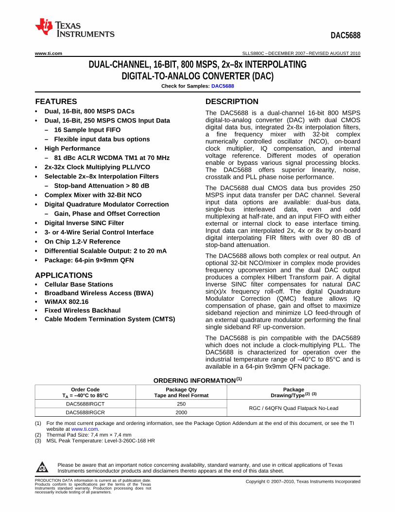
Figure 7. Two Tone IMD vs Intermediate Frequency Figure 8. Two Tone IMD Spectral Plot
10 Submit Documentation Feedback Copyright © 2007–2010, Texas Instruments Incorporated
Product Folder Link(s): DAC5688
-90
-80
-70
-60
-50
-40
-30
-20
-10
0
138 139 140
IF - MHz
Po
wer
- d
Bm
141 142-100
Fdata = 200 MSPS, IQF = 0 MHz
IF = 140 MHzx4 Interpolation, FMIXPLL off
IN
IF (MHz)
55
60
65
70
75
80
85
0 50 100 150 200 250 300 350
AC
LR
- d
Bc
PLL OFF
PLL ON
Fdata = 92.16 MSPS
IF = FNCO
x8 InterpolationFdac = 737.28 MSPS
DAC5688
www.ti.com SLLS880C –DECEMBER 2007–REVISED AUGUST 2010
TYPICAL CHARACTERISTICS (continued)
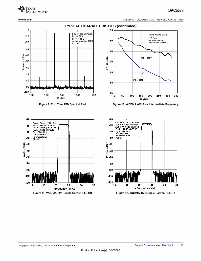
Figure 9. Two Tone IMD Spectral Plot Figure 10. WCDMA ACLR vs Intermediate Frequencyvertical spacervertical spacervertical spacer
Figure 11. WCDMA TM1:Single Carrier, PLL Off Figure 12. WCDMA TM1:Single Carrier, PLL On
Copyright © 2007–2010, Texas Instruments Incorporated Submit Documentation Feedback 11
Product Folder Link(s): DAC5688

DAC5688
SLLS880C –DECEMBER 2007–REVISED AUGUST 2010 www.ti.com
TYPICAL CHARACTERISTICS (continued)
Figure 13. WCDMA TM1:Single Carrier, PLL Off Figure 14. WCDMA TM1:Single Carrier, PLL Onvertical spacervertical spacervertical spacer
Figure 15. WCDMA TM1:Two Carriers, PLL Off Figure 16. WCDMA TM1:Two Carriers, PLL On
12 Submit Documentation Feedback Copyright © 2007–2010, Texas Instruments Incorporated
Product Folder Link(s): DAC5688

DAC5688
www.ti.com SLLS880C –DECEMBER 2007–REVISED AUGUST 2010
TYPICAL CHARACTERISTICS (continued)
Figure 17. WCDMA TM1:Four Carriers, PLL Off Figure 18. WCDMA TM1:Four Carriers, PLL On
Copyright © 2007–2010, Texas Instruments Incorporated Submit Documentation Feedback 13
Product Folder Link(s): DAC5688

DAC5688
SLLS880C –DECEMBER 2007–REVISED AUGUST 2010 www.ti.com
TEST METHODOLOGY
Typical AC specifications were characterized with the DAC5688EVM. A sinusoidal master clock frequency isgenerated by an HP8665B signal generator which drives an Agilent 8133A pulse generator to generate a squarewave output clock for the TSW3100 Pattern Generator and EVM input clock. On the EVM, the input clock isdriven by an CDCM7005 clock distribution chip that is configured to simply buffer the external clock or divide itdown for necessary test configurations.
The DAC5688 output is characterized with a Rohde and Schwarz FSU spectrum analyzer. For WCDMA signalcharacterization, it is important to use a spectrum analyzer with high IP3 and noise subtraction capability so thatthe spectrum analyzer does not limit the ACPR measurement.
DEFINITION OF SPECIFICATIONS
Adjacent Carrier Leakage Ratio (ACLR): Defined for a 3.84Mcps 3GPP W-CDMA input signal measured in a3.84MHz bandwidth at a 5MHz offset from the carrier with a 12dB peak-to-average ratio.
Analog and Digital Power Supply Rejection Ratio (APSRR, DPSRR): Defined as the percentage error in theratio of the delta IOUT and delta supply voltage normalized with respect to the ideal IOUT current.
Differential Nonlinearity (DNL): Defined as the variation in analog output associated with an ideal 1 LSBchange in the digital input code.
Gain Drift: Defined as the maximum change in gain, in terms of ppm of full-scale range (FSR) per °C, from thevalue at ambient (25°C) to values over the full operating temperature range.
Gain Error: Defined as the percentage error (in FSR%) for the ratio between the measured full-scale outputcurrent and the ideal full-scale output current.
Integral Nonlinearity (INL): Defined as the maximum deviation of the actual analog output from the ideal output,determined by a straight line drawn from zero scale to full scale.
Intermodulation Distortion (IMD3, IMD): The two-tone IMD3 or four-tone IMD is defined as the ratio (in dBc) ofthe worst 3rd-order (or higher) intermodulation distortion product to either fundamental output tone.
Offset Drift: Defined as the maximum change in DC offset, in terms of ppm of full-scale range (FSR) per °C,from the value at ambient (25°C) to values over the full operating temperature range.
Offset Error: Defined as the percentage error (in FSR%) for the ratio between the measured mid-scale outputcurrent and the ideal mid-scale output current.
Output Compliance Range: Defined as the minimum and maximum allowable voltage at the output of thecurrent-output DAC. Exceeding this limit may result reduced reliability of the device or adversely affectingdistortion performance.
Reference Voltage Drift: Defined as the maximum change of the reference voltage in ppm per degree Celsiusfrom value at ambient (25°C) to values over the full operating temperature range.
Spurious Free Dynamic Range (SFDR): Defined as the difference (in dBc) between the peak amplitude of theoutput signal and the peak spurious signal.
Signal to Noise Ratio (SNR): Defined as the ratio of the RMS value of the fundamental output signal to theRMS sum of all other spectral components below the Nyquist frequency, including noise, but excluding the firstsix harmonics and dc.
14 Submit Documentation Feedback Copyright © 2007–2010, Texas Instruments Incorporated
Product Folder Link(s): DAC5688

DAC5688
www.ti.com SLLS880C –DECEMBER 2007–REVISED AUGUST 2010
REGISTER DESCRIPTIONS
Table 1. Register MapName Address Default (MSB) Bit 6 Bit 5 Bit 4 Bit 3 Bit 2 Bit 1 (LSB)
Bit 7 Bit 0
STATUS0 0x00 0x01 PLL_lock unused unused device_ID(2:0) version(1:0)
CONFIG1 0x01 0x0B insel_mode(1:0) unused synchr_clkin twos inv_inclk interp_value(1:0)
CONFIG2 0x02 0xE1 diffclk_ena clk1_in_ena clk1c_in_ena clko_SE_hold fir4_ena qmc_offset_ena qmc_corr_ena mixer_ena
CONFIG3 0x03 0x00 diffclk_dly(1:0) clko_dly(1:0) reserved
CONFIG4 0x04 0x00 ser_dac_data_ena output_delay(1:0) B_equals_A A_equals_B unused reva revb
CONFIG5 0x05 0x22 sif4 sif_sync_sig clkdiv_sync_ena clkdiv_sync_sel reserved clkdiv_shift mixer_gain unused
CONFIG6 0x06 0x00 phaseoffset(7:0)
CONFIG7 0x07 0x00 phaseoffset(15:8)
CONFIG8 0x08 0x00 phaseadd(7:0)
CONFIG9 0x09 0x00 phaseadd(15:8)
CONFIG10 0x0A 0x00 phaseadd(23:16)
CONFIG11 0x0B 0x00 phaseadd(31:24)
CONFIG12 0x0C 0x00 qmc_gaina(7:0)
CONFIG13 0x0D 0x00 qmc_gainb(7:0)
CONFIG14 0x0E 0x00 qmc_phase(7:0)
CONFIG15 0x0F 0x24 qmc_phase(9:8) qmc_gaina(10:8) qmc_gainb(10:8)
CONFIG16 0x10 0x00 qmc_offseta(7:0)
CONFIG17 0x11 0x00 qmc_offsetb(7:0)
CONFIG18 0x12 0x00 qmc_offseta(12:8) unused unused unused
CONFIG19 0x13 0x00 qmc_offsetb(12:8) unused unused unused
CONFIG20 0x14 0x00 ser_dac_data(7:0)
CONFIG21 0x15 0x00 ser_dac_data(15:8)
CONFIG22 0x16 0x15 nco_sel(1:0) nco_reg_sel(1:0) qmcorr_reg_sel(1:0) qmoffset_reg_sel(1:0)
CONFIG23 0x17 0x15 unused unused fifo_sel(2:0) aflag_sel unused unused
CONFIG24 0x18 0x80 fifo_sync_strt(3:0) unused unused unused unused
CONFIG25 0x19 0x00 unused unused unused unused unused unused unused unused
CONFIG26 0x1A 0x0D io_1p8_3p3 unused sleepb sleepa isbiaslpf_a isbiaslpf_b PLL_sleep PLL_ena
CONFIG27 0x1B 0xFF coarse_daca(3:0) coarse_dacb(3:0)
CONFIG28 0x1C 0x00 reserved
CONFIG29 0x1D 0x00 PLL_m(4:0) PLL_n(2:0)
CONFIG30 0x1E 0x00 PLL_LPF_reset VCO_div2 PLL_gain(1:0) PLL_range(3:0)
Copyright © 2007–2010, Texas Instruments Incorporated Submit Documentation Feedback 15
Product Folder Link(s): DAC5688

DAC5688
SLLS880C –DECEMBER 2007–REVISED AUGUST 2010 www.ti.com
Register name: STATUS0 - Address: 0x00, Default 0x01Bit 7 Bit 6 Bit 5 Bit 4 Bit 3 Bit 2 Bit 1 Bit 0
PLL_lock unused unused device_ID (2:0) version(1:0)
0 0 0 0 0 0 0 1
PLL_lock : Asserted when the internal PLL is locked. (Read Only)
device_ID(2:0) : Returns ‘000’ for DAC5688. (Read Only)
version(1:0) : A hardwired register that contains the version of the chip. (Read Only)
Register name: CONFIG1 Address: 0x01, Default 0x0BBit 7 Bit 6 Bit 5 Bit 4 Bit 3 Bit 2 Bit 1 Bit 0
insel_mode (1:0) unused synchr_clkin twos inv_inclk interp_valule(1:0)
0 0 0 0 1 0 1 1
insel_mode(1:0) : Controls the expected format of the input data. For the interleaved modes, TXENABLE or the MSB of the portthat does not have data can be used to tell the chip which sample is the A sample. For TXENABLE the samplealigned with the rising edge is A. For the MSB, it is presumed that this signal will toggle with A and B. The MSBshould be ‘1’ for A and ‘0’ for B. (*** See CONFIG23 ***)
insel_mode Function
00 Normal input on A and B.
01 Interleaved input on A, which is de-interleaved and placed onboth A and B data paths. (*** See CONFIG23 ***)
10 Interleaved input on B, which is de-interleaved and placed onboth A and B data paths. (*** See CONFIG23 ***)
11 Half rate data on A and B inputs. This data is merge togetherto form a single stream of data on the A data path.
synchr_clkin : This turns on the synchronous mode of the dual-clock in mode. In this mode, the CLK2/C and CLK1/C must besynchronous in phase since the slower clock is used to synchronize dividers in the clock distribution circuit.
twos : When set (default), the input data format is expected to be 2’s complement. When cleared, the input isexpected to be offset-binary.
inv_inclk : This allows the input clock, the clock driving the input side of the FIFO to be inverted. This allows easierregistering of the data (more setup/hold time) in the single-clock mode of the device
interp_value(1:0) : These bits define the interpolation factor:
interp_value Interpolation Factor
00 1X
01 2X
10 4X
11 8X
16 Submit Documentation Feedback Copyright © 2007–2010, Texas Instruments Incorporated
Product Folder Link(s): DAC5688
DAC5688
www.ti.com SLLS880C –DECEMBER 2007–REVISED AUGUST 2010
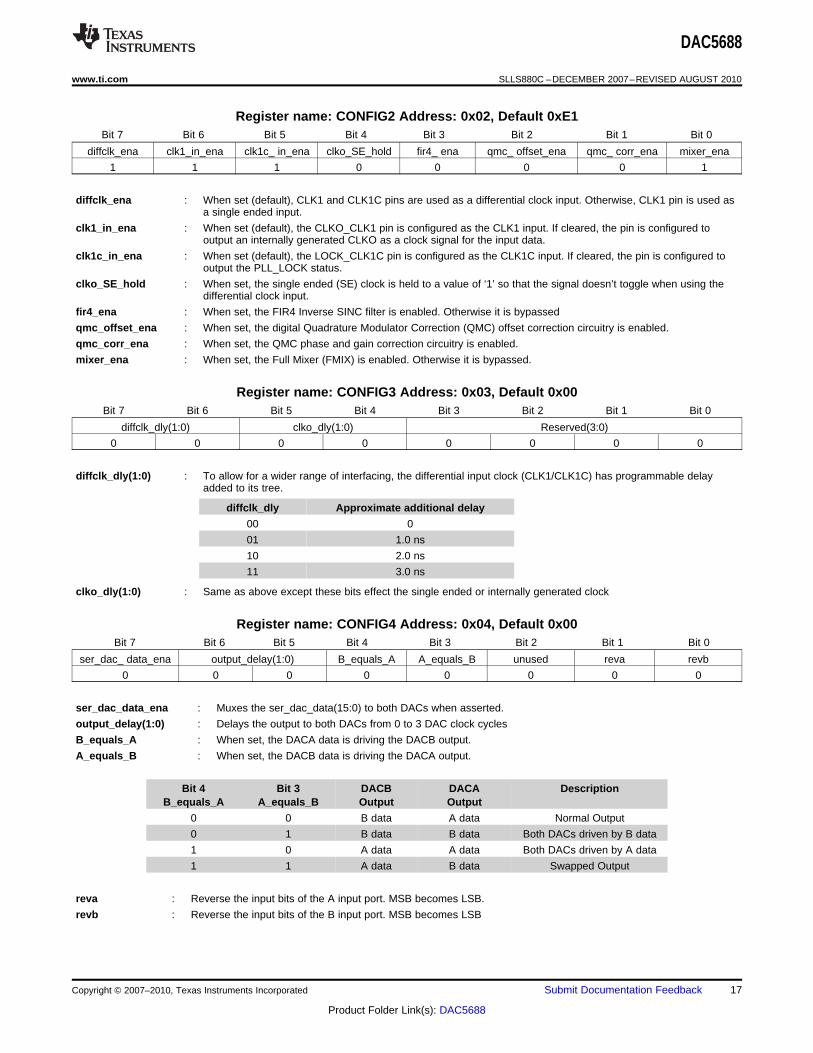
Register name: CONFIG2 Address: 0x02, Default 0xE1Bit 7 Bit 6 Bit 5 Bit 4 Bit 3 Bit 2 Bit 1 Bit 0
diffclk_ena clk1_in_ena clk1c_ in_ena clko_SE_hold fir4_ ena qmc_ offset_ena qmc_ corr_ena mixer_ena
1 1 1 0 0 0 0 1
diffclk_ena : When set (default), CLK1 and CLK1C pins are used as a differential clock input. Otherwise, CLK1 pin is used asa single ended input.
clk1_in_ena : When set (default), the CLKO_CLK1 pin is configured as the CLK1 input. If cleared, the pin is configured tooutput an internally generated CLKO as a clock signal for the input data.
clk1c_in_ena : When set (default), the LOCK_CLK1C pin is configured as the CLK1C input. If cleared, the pin is configured tooutput the PLL_LOCK status.
clko_SE_hold : When set, the single ended (SE) clock is held to a value of ‘1’ so that the signal doesn’t toggle when using thedifferential clock input.
fir4_ena : When set, the FIR4 Inverse SINC filter is enabled. Otherwise it is bypassed
qmc_offset_ena : When set, the digital Quadrature Modulator Correction (QMC) offset correction circuitry is enabled.
qmc_corr_ena : When set, the QMC phase and gain correction circuitry is enabled.
mixer_ena : When set, the Full Mixer (FMIX) is enabled. Otherwise it is bypassed.
Register name: CONFIG3 Address: 0x03, Default 0x00Bit 7 Bit 6 Bit 5 Bit 4 Bit 3 Bit 2 Bit 1 Bit 0
diffclk_dly(1:0) clko_dly(1:0) Reserved(3:0)
0 0 0 0 0 0 0 0
diffclk_dly(1:0) : To allow for a wider range of interfacing, the differential input clock (CLK1/CLK1C) has programmable delayadded to its tree.
diffclk_dly Approximate additional delay
00 0
01 1.0 ns
10 2.0 ns
11 3.0 ns
clko_dly(1:0) : Same as above except these bits effect the single ended or internally generated clock
Register name: CONFIG4 Address: 0x04, Default 0x00Bit 7 Bit 6 Bit 5 Bit 4 Bit 3 Bit 2 Bit 1 Bit 0
ser_dac_ data_ena output_delay(1:0) B_equals_A A_equals_B unused reva revb
0 0 0 0 0 0 0 0
ser_dac_data_ena : Muxes the ser_dac_data(15:0) to both DACs when asserted.
output_delay(1:0) : Delays the output to both DACs from 0 to 3 DAC clock cycles
B_equals_A : When set, the DACA data is driving the DACB output.
A_equals_B : When set, the DACB data is driving the DACA output.
Bit 4 Bit 3 DACB DACA DescriptionB_equals_A A_equals_B Output Output
0 0 B data A data Normal Output
0 1 B data B data Both DACs driven by B data
1 0 A data A data Both DACs driven by A data
1 1 A data B data Swapped Output
reva : Reverse the input bits of the A input port. MSB becomes LSB.
revb : Reverse the input bits of the B input port. MSB becomes LSB
Copyright © 2007–2010, Texas Instruments Incorporated Submit Documentation Feedback 17
Product Folder Link(s): DAC5688

DAC5688
SLLS880C –DECEMBER 2007–REVISED AUGUST 2010 www.ti.com
Register name: CONFIG5 Address: 0x05, Default 0x22Bit 7 Bit 6 Bit 5 Bit 4 Bit 3 Bit 2 Bit 1 Bit 0
sif4 sif_ sync_sig clkdiv_sync_ena clkdiv_sync_sel Reserved clkdiv_shift mixer_gain unused
0 0 1 0 0 0 1 0
sif4 : When set, the serial interface (SIF) is a 4 bit interface, otherwise it is a 3 bit interface.
sif_sync_sig : SIF created sync signal. Set to ‘1’ to cause a sync and then clear to ‘0’ to remove it.
clkdiv_sync_ena : Enables syncing of the clock divider using the sync or TXENABLE pins when the bit is asserted.
clkdiv_sync_sel : Selects the input pin to sync the clock dividers. (0 = SYNC, 1 = TXENABLE)
clkdiv_shift : When set, a rising edge on the selected sync (see clkdiv_sync_sel) for the clock dividers will cause a slip in thesynchronous counter by 1T and is useful for multi-DAC time alignment.
mixer_gain : When set, adds 6dB to the mixer gain output.
Register name: CONFIG6 Address: 0x06, Default 0x00 (Synced)Bit 7 Bit 6 Bit 5 Bit 4 Bit 3 Bit 2 Bit 1 Bit 0
phaseoffset(7:0)
0 0 0 0 0 0 0 0
phaseoffset(7:0) : See CONFIG7 below.
Register name: CONFIG7 Address: 0x07, Default 0x00 (Synced)Bit 7 Bit 6 Bit 5 Bit 4 Bit 3 Bit 2 Bit 1 Bit 0
phaseoffset(15:8)
0 0 0 0 0 0 0 0
phaseoffset(15:8) : This is the phase offset added to the NCO accumulator just before generation of the SIN and COS values. Thephase offset is added to the upper 16bits of the NCO accumulator results and these 16 bits are used in thesin/cosine lookup tables.
Register name: CONFIG8 Address: 0x08, Default 0x00 (Synced)Bit 7 Bit 6 Bit 5 Bit 4 Bit 3 Bit 2 Bit 1 Bit 0
phaseadd(7:0)
0 0 0 0 0 0 0 0
phaseadd(7:0) : See CONFIG11 below.
Register name: CONFIG9 Address: 0x09, Default 0x00 (Synced)Bit 7 Bit 6 Bit 5 Bit 4 Bit 3 Bit 2 Bit 1 Bit 0
phaseadd(15:8)
0 0 0 0 0 0 0 0
phaseadd(15:8) : See CONFIG11 below.
Register name: CONFIG10 Address: 0x0A, Default 0x00 (Synced)Bit 7 Bit 6 Bit 5 Bit 4 Bit 3 Bit 2 Bit 1 Bit 0
phaseadd(23:16)
0 0 0 0 0 0 0 0
phaseadd(23:16) : See CONFIG11 below.
18 Submit Documentation Feedback Copyright © 2007–2010, Texas Instruments Incorporated
Product Folder Link(s): DAC5688
DAC5688
www.ti.com SLLS880C –DECEMBER 2007–REVISED AUGUST 2010
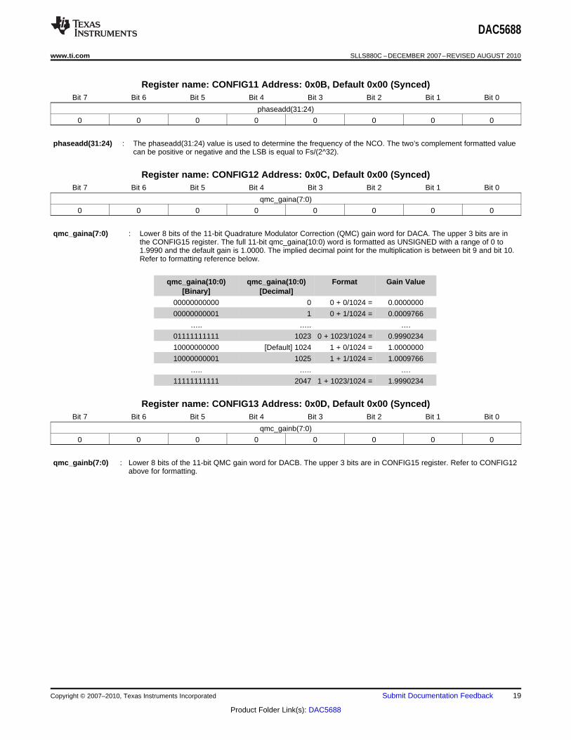
Register name: CONFIG11 Address: 0x0B, Default 0x00 (Synced)Bit 7 Bit 6 Bit 5 Bit 4 Bit 3 Bit 2 Bit 1 Bit 0
phaseadd(31:24)
0 0 0 0 0 0 0 0
phaseadd(31:24) : The phaseadd(31:24) value is used to determine the frequency of the NCO. The two’s complement formatted valuecan be positive or negative and the LSB is equal to Fs/(2^32).
Register name: CONFIG12 Address: 0x0C, Default 0x00 (Synced)Bit 7 Bit 6 Bit 5 Bit 4 Bit 3 Bit 2 Bit 1 Bit 0
qmc_gaina(7:0)
0 0 0 0 0 0 0 0
qmc_gaina(7:0) : Lower 8 bits of the 11-bit Quadrature Modulator Correction (QMC) gain word for DACA. The upper 3 bits are inthe CONFIG15 register. The full 11-bit qmc_gaina(10:0) word is formatted as UNSIGNED with a range of 0 to1.9990 and the default gain is 1.0000. The implied decimal point for the multiplication is between bit 9 and bit 10.Refer to formatting reference below.
qmc_gaina(10:0) qmc_gaina(10:0) Format Gain Value[Binary] [Decimal]
00000000000 0 0 + 0/1024 = 0.0000000
00000000001 1 0 + 1/1024 = 0.0009766
….. ….. ….
01111111111 1023 0 + 1023/1024 = 0.9990234
10000000000 [Default] 1024 1 + 0/1024 = 1.0000000
10000000001 1025 1 + 1/1024 = 1.0009766
….. ….. ….
11111111111 2047 1 + 1023/1024 = 1.9990234
Register name: CONFIG13 Address: 0x0D, Default 0x00 (Synced)Bit 7 Bit 6 Bit 5 Bit 4 Bit 3 Bit 2 Bit 1 Bit 0
qmc_gainb(7:0)
0 0 0 0 0 0 0 0
qmc_gainb(7:0) : Lower 8 bits of the 11-bit QMC gain word for DACB. The upper 3 bits are in CONFIG15 register. Refer to CONFIG12above for formatting.
Copyright © 2007–2010, Texas Instruments Incorporated Submit Documentation Feedback 19
Product Folder Link(s): DAC5688

DAC5688
SLLS880C –DECEMBER 2007–REVISED AUGUST 2010 www.ti.com
Register name: CONFIG14 Address: 0x0E, Default 0x00 (Synced)Bit 7 Bit 6 Bit 5 Bit 4 Bit 3 Bit 2 Bit 1 Bit 0
qmc_phase(7:0)
0 0 0 0 0 0 0 0
qmc_phase(7:0) : Lower 8 bits of the 10-bit Quadrature Modulator Correction (QMC) phase word. The upper 2 bits are in theCONFIG15 register. The full 11-bit qmc_phase(9:0) correction word is formatted as two’s complement andscaled to occupy a range of –0.125 to 0.12475 and a default phase correction 0.00. To accomplish QMC phasecorrection, this value is multiplied by the current ‘Q’ sample, then summed into the ‘I’ sample. Refer to formattingreference below.
qmc_phase(9:0) qmc_phase(9:0) Format Phase[Binary] [Decimal] Correction
10000000000 –512 (–1 + 0/512) / 8 = –0.1250000
10000000001 –511 (–1 + 1/512) / 8 = –0.1234559
….. ….. ….
11111111111 –1 (–1 + 511/512) / 8 = –0.0002441
00000000000 [Default] 0 (+0 + 0/512) / 8 = +0.0000000
00000000001 1 (+0 + 1/512) / 8 = +0.0002441
….. ….. ….
01111111111 511 (+0 + 511/512) / 8 = +0.1247559
Register name: CONFIG15 Address: 0x0F, Default 0x24 (Synced)Bit 7 Bit 6 Bit 5 Bit 4 Bit 3 Bit 2 Bit 1 Bit 0
qmc_phase(9:8) qmc_gaina(10:8) qmc_gainb(10:8)
0 0 1 0 0 1 0 0
qmc_phase(9:8) : Upper 2 bits of qmc_phase term. Defaults to zero.
qmc_gaina(10:8) : Upper 3 bits of qmc_gaina term. Defaults to unity gain.
qmc_gainb(10:8) : Upper 3 bits of the qmc_gainb term. Defaults to unity gain.
Register name: CONFIG16 Address: 0x10, Default 0x00 (Synced)Bit 7 Bit 6 Bit 5 Bit 4 Bit 3 Bit 2 Bit 1 Bit 0
qmc_offseta(7:0)
0 0 0 0 0 0 0 0
qmc_offseta(7:0) : Lower 8 bits of the DACA offset correction. The upper 5 bits are in CONFIG18 register. The offset ismeasured in DAC LSBs.
Register name: CONFIG17 Address: 0x11, Default 0x00 (Synced)Bit 7 Bit 6 Bit 5 Bit 4 Bit 3 Bit 2 Bit 1 Bit 0
qmc_offsetb(7:0)
0 0 0 0 0 0 0 0
qmc_offsetb(7:0) : Lower 8 bits of the DACB offset correction. The upper 5 bits are inCONFIG19 register. The offset is measured in DAC LSBs.
20 Submit Documentation Feedback Copyright © 2007–2010, Texas Instruments Incorporated
Product Folder Link(s): DAC5688

DAC5688
www.ti.com SLLS880C –DECEMBER 2007–REVISED AUGUST 2010
Register name: CONFIG18 Address: 0x12, Default 0x00 (Synced)Bit 7 Bit 6 Bit 5 Bit 4 Bit 3 Bit 2 Bit 1 Bit 0
qmc_offseta(12:8) unused unused unused
0 0 0 0 0 0 0 0
qmc_offseta(12:8) : Upper 5 bits of the DACA offset correction.
Register name: CONFIG19 Address: 0x13, Default 0x00 (Synced)Bit 7 Bit 6 Bit 5 Bit 4 Bit 3 Bit 2 Bit 1 Bit 0
qmc_offsetb(12:8) unused unused unused
0 0 0 0 0 0 0 0
qmc_offsetb(12:8) : Upper 5 bits of the DACB offset correction.
Register name: CONFIG20 Address: 0x14, Default 0x00Bit 7 Bit 6 Bit 5 Bit 4 Bit 3 Bit 2 Bit 1 Bit 0
ser_dac_data(7:0)
0 0 0 0 0 0 0 0
ser_dac_data(7:0) : Lower 8 bits of the serial interface controlled DAC value. This data is routed to both DACs when enabledvia ser_dac_data_ena in CONFIG4. Value is expected in 2s complement format.
Register name: CONFIG21 Address: 0x15, Default 0x00Bit 7 Bit 6 Bit 5 Bit 4 Bit 3 Bit 2 Bit 1 Bit 0
ser_dac_data(15:8)
0 0 0 0 0 0 0 0
ser_dac_data(15:8) : Upper 8 bits of the serial interface controlled DAC value. This data is routed to both DACs when enabled viaser_dac_data_ena in CONFIG4. Value is expected in 2's complement format.
Register name: CONFIG22 Address: 0x16, Default 0x15Bit 7 Bit 6 Bit 5 Bit 4 Bit 3 Bit 2 Bit 1 Bit 0
nco_sel(1:0) nco_reg_sel(1:0) qmcorr_reg_sel(1:0) qmoffset_reg_sel(1:0)
0 0 0 1 0 1 0 1
nco_sel(1:0) : Selects the signal to use as the sync for the NCO accumulator.
nco_reg_sel(1:0) : Selects the signal to use as the sync for loading the NCO registers.
qmcorr_reg_sel(1:0) : Selects the signal to use as the sync for loading the QM correction registers.
qmoffsest_reg_sel(1:0) : Selects the signal to use as the sync for loading the QM offset correction registers.
*_sel (1:0) Sync selected
00 TXENABLE from FIFO output
01 SYNC from FIFO output
10 sync_SIF_sig (via CONFIG5)
11 Always zero
Copyright © 2007–2010, Texas Instruments Incorporated Submit Documentation Feedback 21
Product Folder Link(s): DAC5688

DAC5688
SLLS880C –DECEMBER 2007–REVISED AUGUST 2010 www.ti.com
Register name: CONFIG23 Address: 0x17, Default 0x15Bit 7 Bit 6 Bit 5 Bit 4 Bit 3 Bit 2 Bit 1 Bit 0
unused unused fifo_sel(2:0) aflag_ sel unused unused
0 0 0 1 0 1 0 1
fifo_sel(2:0) : Selects the sync source for the FIFO from the table below. For the case where the sync is dependent on the firsttransition of the input data MSB: Once the transition occurs, the only way to get another sync it to reset the deviceor to program fifo_sel to another value
fifo_sel (2:0) Sync selected
000 TXENABLE from pin
001 SYNC from pin
010 sync_SIF_sig (via CONFIG5)
011 Always zero
100 1st transition on DA MSB
101 1st transition on DB MSB
110 Always zero
111 Always one
aflag_sel : When set, the MSB of the input opposite of incoming data is used to determine the A sample. When cleared,rising edge of TXENABLE is used. Refer to Figure 37.
Register name: CONFIG24 Address: 0x18, Default 0x80Bit 7 Bit 6 Bit 5 Bit 4 Bit 3 Bit 2 Bit 1 Bit 0
fifo_sync_strt(3:0) Unused Unused Unused Unused
1 0 0 0 0 0 0 0
fifo_sync_strt(3:0) : When the sync to the FIFO occurs, this is the value loaded into the FIFO output position counter. With thisvalue the initial difference between input and output pointers can be controlled. This may be helpful insyncing multiple chips or controlling the delay through the device.
Register name: CONFIG25 Address: 0x19, Default 0x00Bit 7 Bit 6 Bit 5 Bit 4 Bit 3 Bit 2 Bit 1 Bit 0
Unused Unused Unused Unused Unused Unused Unused Unused
0 0 0 0 0 0 0 0
Register name: CONFIG26 Address: 0x1A, Default 0x0DBit 7 Bit 6 Bit 5 Bit 4 Bit 3 Bit 2 Bit 1 Bit 0
io_1p8_3p3 Unused sleepb sleepa isbiaslpfb_a isbiaslpf_b PLL_ sleep PLL_ena
0 0 0 0 1 1 0 1
io_1p8_3p3 : Used to program the digital input voltage threshold levels. ‘0’=3.3V tolerate pads and ‘1’=1.8V tolerate pads.Applies to following digital pins: CLKO_CLK1, LOCK_CLK1C, DA[15:0], DB[15:0], SYNC, RESETB, SCLK,SDENB, SDIO (input only) and TXENABLE.
sleepb : When set, DACB is put into sleep mode. Putting the DAC into single DAC mode does not automatically assert thissignal, so for minimum power in single DAC mode, also program this register bit.
sleepa : When set, DACA is put into sleep mode. Note: If DACA channel is in sleep mode (sleepa = '1') the DACB channelis also forced in to sleep mode.
isbiaslpfb_a : Turns on the low pass filter for the current source bias in the DACA when cleared. The low pass filter will set acorner at ~472kHz when low and ~95 kHz when high.
isbiaslpfb_b : Turns on the low pass filter for the current source bias in the DACB when cleared. The low pass filter will set acorner at ~472kHz when low and ~95 kHz when high.
PLL_sleep : When set, the PLL is put into sleep mode. Bypassing the PLL does not automatically but it into sleep mode.
PLL_ena : When set, the PLL is on and its output clock is being used as the DAC clock.
22 Submit Documentation Feedback Copyright © 2007–2010, Texas Instruments Incorporated
Product Folder Link(s): DAC5688

VEXTIORbias
(DACA_gain 1)
ƒvco (M)(N) ƒref
DAC5688
www.ti.com SLLS880C –DECEMBER 2007–REVISED AUGUST 2010
Register name: CONFIG27 Address: 0x1B, Default 0xFFBit 7 Bit 6 Bit 5 Bit 4 Bit 3 Bit 2 Bit 1 Bit 0
coarse_daca(3:0) coarse_dacb(3:0)
1 1 1 1 1 1 1 1
coarse_daca(3:0) : Scales the output current is 16 equal steps.
coarse_dacb(3:0) : Same as above except for DACB.
Register name: CONFIG28 Address: 0x1C, Default 0x00Bit 7 Bit 6 Bit 5 Bit 4 Bit 3 Bit 2 Bit 1 Bit 0
Reserved Reserved Reserved Reserved Reserved Reserved Reserved Reserved
0 0 0 0 0 0 0 0
Register name: CONFIG29 Address: 0x1D, Default 0x00Bit 7 Bit 6 Bit 5 Bit 4 Bit 3 Bit 2 Bit 1 Bit 0
PLL_m(4:0) PLL_n(2:0)
0 0 0 0 0 0 0 0
PLL_m : M portion of the M/N divider of the PLL thermometer encoded:
PLL_m(4:0) M value
00000 1
00001 2
00011 4
00111 8
01111 16
11111 32
All other values Invalid
PLL_n : N portion of the M/N divider of the PLL thermometer encoded. If supplying a high rate CLK2/C frequency, the PLL_n valueshould be used to divide down the input CLK2/C to maintain a maximum PFD operating of 160 MHz.
PLL_n(2:0) n value
000 1
001 2
011 4
111 8
All other values Invalid
PLL Function:
where ƒref is the frequency of the external DAC clock input on the CLK2/C pins
Copyright © 2007–2010, Texas Instruments Incorporated Submit Documentation Feedback 23
Product Folder Link(s): DAC5688

DAC5688
SLLS880C –DECEMBER 2007–REVISED AUGUST 2010 www.ti.com
Register name: CONFIG30 Address: 0x1E, Default 0x00Bit 7 Bit 6 Bit 5 Bit 4 Bit 3 Bit 2 Bit 1 Bit 0
PLL_LPF_ reset VCO_div2 PLL_gain(1:0) PLL_range(3:0)
0 0 0 0 0 0 0 0
PLL_LPF_reset : When set, can be used to hold the PLL loop filter at 0 volts.
VCO_div2 : When set, the PLL CLOCK output is 1/2 the PLL VCO frequency. Used to run the VCO at 2X the desired clockfrequency to reduce phase noise for lower DAC clock rates.
PLL_gain(1:0) : Used to adjust the PLL’s Voltage Controlled Oscillator (VCO) gain, KVCO. Refer to the Electrical Characteristicstable. By increasing the PLL_gain, the VCO can cover a broader range of frequencies; however, the higher gainalso increases the phase noise of the PLL. In general, lower PLL_gain settings result in lower phase noise. TheKVCO of the VCO can also affect the PLL stability and is used to determine the loop filter components. See sectionon determining the PLL filter components for more detail.
PLL_range(3:0) : Used to adjust the bias current of the VCO. By increasing the bias current, the oscillator can reach higherfrequencies. Refer to the Electrical Characteristics table.'0000' – minimum bias current and lowest VCO frequency range'1111' – maximum bias current and highest VCO frequency range
24 Submit Documentation Feedback Copyright © 2007–2010, Texas Instruments Incorporated
Product Folder Link(s): DAC5688

VCON-Divider
ChargePumpR-
Div
Status& Control
PFD
10 MHzREFOSC
REF_INCPOUT
VCTRL_IN
900
TRF3703 AQM
DAC
DAC
LPF
NC
O/M
ixe
r
I/Q
FIR
1-3
(8x)
CL
K2
opt.PLL
LoopFilter
100
DAC5688 DAC
PLLSynth
TRF3761-X PLL/VCO
LoopFilter
÷1÷8
Status &Control VCXO
CL
K2
C
LoopFilter
Div1/2/4
Clock Divider /Distribution
CDCM7005
5V
5V
614.4 MHz
76.8 MHz
614.4 MHz
~ 2.1 GHz
Term
CLK1
DA[15:0]
GC5016
PA
Du
plex
er
Antenna
To TXFeedback
To RXPath
LPF
I-Signal
Q-Signal
Term
Term
TXENABLE
QM
C(G
ain
/Pha
se)
InvS
INC
FIF
O&
De
mu
x
Clock, Sync & Control
÷8
76.8 MHz
CK
DigitalUp
Converter(DUC)
DB[15:0]
16
16
DAC5688
www.ti.com SLLS880C –DECEMBER 2007–REVISED AUGUST 2010
DETAILED DESCRIPTION
EXAMPLE SYSTEM DIAGRAM
Figure 19. Example System Diagram: Direct Conversion with 8x interpolation
SERIAL INTERFACE
The serial port of the DAC5688 is a flexible serial interface which communicates with industry standardmicroprocessors and microcontrollers. The interface provides read/write access to all registers used to define theoperating modes of DAC5688. It is compatible with most synchronous transfer formats and can be configured asa 3 or 4 pin interface by SIF4 in register CONFIG5. In both configurations, SCLK is the serial interface inputclock and SDENB is serial interface enable. For 3 pin configuration, SDIO is a bidirectional pin for both data inand data out. For 4 pin configuration, SDIO is data in only and SDO is data out only. Data is input into the devicewith the rising edge of SCLK. Data is output from the device on the falling edge of SCLK.
Each read/write operation is framed by signal SDENB (Serial Data Enable Bar) asserted low for 2 to 5 bytes,depending on the data length to be transferred (1–4 bytes). The first frame byte is the instruction cycle whichidentifies the following data transfer cycle as read or write, how many bytes to transfer, and what address totransfer the data. Table 2 indicates the function of each bit in the instruction cycle and is followed by a detaileddescription of each bit. Frame bytes 2 to 5 comprise the data transfer cycle.
Copyright © 2007–2010, Texas Instruments Incorporated Submit Documentation Feedback 25
Product Folder Link(s): DAC5688

SDENB
SCLK
Instruction Cycle Data Transfer Cycle(s)
SDIO r/w N1 N0 A4 A3 A2 A1 A0 D7 D6 D5 D4 D3 D2 D1 D0
SDENB
SCLK
SDIO
t s (SDENB)
t s (SDIO)
t h (SDIO)
t SCLK
t SCLKH tSCLKL
DAC5688
SLLS880C –DECEMBER 2007–REVISED AUGUST 2010 www.ti.com
Table 2. Instruction Byte of the Serial InterfaceBit 7 6 5 4 3 2 1 0
Description R/W N1 N0 A4 A3 A2 A1 A0
R/W Identifies the following data transfer cycle as a read or write operation. A high indicates a read operation from DAC5688 anda low indicates a write operation to DAC5688.
[N1 : N0] Identifies the number of data bytes to be transferred per Table 3. Data is transferred MSB first.
Table 3. Number of Transferred Bytes Within OneCommunication Frame
N1 N0 Description
0 0 Transfer 1 Byte
0 1 Transfer 2 Bytes
1 0 Transfer 3 Bytes
1 1 Transfer 4 Bytes
[A4 : A0] Identifies the address of the register to be accessed during the read or write operation. For multi-byte transfers, this addressis the starting address. Note that the address is written to the DAC5688 MSB first and counts down for each byte
Figure 20 shows the serial interface timing diagram for a DAC5688 write operation. SCLK is the serial interfaceclock input to DAC5688. Serial data enable SDENB is an active low input to DAC5688. SDIO is serial data in.Input data to DAC5688 is clocked on the rising edges of SCLK.
Figure 20. Serial Interface Write Timing Diagram
Figure 21 shows the serial interface timing diagram for a DAC5688 read operation. SCLK is the serial interfaceclock input to DAC5688. Serial data enable SDENB is an active low input to DAC5688. SDIO is serial data induring the instruction cycle. In 3 pin configuration, SDIO is data out from DAC5688 during the data transfercycle(s), while SDO is in a high-impedance state. In 4 pin configuration, SDO is data out from DAC5688 duringthe data transfer cycle(s). The SDIO/SDO data is output on the falling edge of SCLK. At the end of the datatransfer, SDO will output low on the final falling edge of SCLK until the rising edge of SDENB when it will 3-state.
26 Submit Documentation Feedback Copyright © 2007–2010, Texas Instruments Incorporated
Product Folder Link(s): DAC5688

D
SDENB
SCLK
SDIO r/w N1 N0 - A3 A2 A1 A0 D7 D6 D5 D4 D3 D2 D1 D0 0
Instruction Cycle Data Transfer Cycle(s)
SDO D7 D6 D5 D4 D3 2 D1 D0 0
3 pin configuration
output
4 pin configuration
outputSDENB
SCLK
SDIO Data n Data n-1
t d (Data)
SDO
DAC5688
www.ti.com SLLS880C –DECEMBER 2007–REVISED AUGUST 2010
Figure 21. Serial Interface Read Timing Diagram
FIR FILTERS
Figure 22 shows the magnitude spectrum response for FIR1, a 67-tap interpolating half-band filter. The transitionband is from 0.4 to 0.6 × fIN (the input data rate for the FIR filter) with <0.002-dB of pass-band ripple and > 80-dBstop-band attenuation. Figure 23 shows the transition band region from 0.37 to 0.47 × fIN. Up to 0.458 × fIN thereis less than 0.5 dB of attenuation.
Figure 24 shows the magnitude spectrum response for the 19-tap FIR2 filter. The transition band is from 0.25 to0.75 × fIN (the input data rate for the FIR filter). For 4x interpolation modes, the composite filter response isshown in Figure 25.
Figure 26 shows the magnitude spectrum response for the 11-tap FIR3 filter. For 8x interpolation modes, thecomposite filter response is shown in Figure 27.
The DAC5688 also has a 9-tap non-interpolating inverse sinc filter (FIR4) running at the DAC update rate (fDAC)that can be used to flatten the frequency response of the sample and hold output. The DAC sample and holdoutput set the output current and holds it constant for one DAC clock cycle until the next sample, resulting in thewell known sin(x)/x or sinc(x) frequency response shown in Figure 28 (red dash-dotted line). The inverse sincfilter response (Figure 28, blue dashed line) has the opposite frequency response between 0 to 0.4 × fDAC,resulting in the combined response (Figure 28, green solid line). Between 0 to 0.4 × fDAC, the inverse sinc filtercompensates the sample and hold rolloff with less than 0.03-dB error.
The inverse sinc filter has a gain > 1 at all frequencies. Therefore, the signal input to FIR4 must be reduced fromfull scale to prevent saturation in the filter. The amount of backoff required depends on the signal frequency, andis set such that at the signal frequencies the combination of the input signal and filter response is less than 1 (0dB). For example, if the signal input to FIR4 is at 0.25 × fDAC, the response of FIR4 is 0.9 dB, and the signal mustbe backed off from full scale by 0.9 dB. The gain function in the QMC block can be used to set reduce amplitudeof the input signal. The advantage of FIR4 having a positive gain at all frequencies is that the user is then able tooptimized backoff of the signal based on the signal frequency.
The filter taps for all digital filters are listed in Table 4. Note that the loss of signal amplitude may result in lowerSNR due to decrease in signal amplitude.
Copyright © 2007–2010, Texas Instruments Incorporated Submit Documentation Feedback 27
Product Folder Link(s): DAC5688

0.1
0
-0.1
-0.2
-0.3
-0.4
-0.5
0.37 0.38 0.39 0.4 0.41 0.42 0.43 0.44 0.45 0.46 0.47
dB
f/Fin
Magnitude Spectrum for FIR120
0
-20
-40
-60
-80
-100
-120
-140
-160
dB
0 0.1 0.2 0.3 0.4 0.5 0.6 0.7 0.8 0.9 1.0
f/Fin
Magnitude Spectrum for FIR1
0
-20
-40
-60
-80
-100
-120
-140
-1600.5 1 2
dB
f/Fin
4x Interpolation Composite Filtering Response
20
0
-20
-40
-60
-80
-100
-120
-140
-1600 0.1 0.2 0.3 0.4 0.5 0.6 0.7 0.8 0.9 1
dB
f/Fin
Magnitude Spectrum for FIR 2
DAC5688
SLLS880C –DECEMBER 2007–REVISED AUGUST 2010 www.ti.com
Figure 22. Magnitude Spectrum for FIR1 Figure 23. FIR1 Transition Bandvertical spacervertical spacervertical spacer
Figure 24. Magnitude Spectrum for FIR2 Figure 25. 4x Interpolation Composite Responsevertical spacervertical spacervertical spacer
28 Submit Documentation Feedback Copyright © 2007–2010, Texas Instruments Incorporated
Product Folder Link(s): DAC5688

0
-20
-40
-60
-80
-100
-120
-140
-160
dB
0.5 1 4f/Fin
8x Interpolation Composite Filtering Response
32
20
0
-20
-40
-60
-80
-100
-120
-140
-160
dB
0 0.1 0.2 0.3 0.4 0.5 0.6 0.7 0.8 0.9 1
f/Fin
Magnitude Spectrum for FIR 3
5
4
3
2
1
0
-1
-2
-3
-4
-5
0 0.05 0.1 0.15 0.2 0.25 0.3 0.35 0.4 0.45 0.5
dB
f/fDAC
FIR 4 Inverse Corrected Spectrum
DAC5688
www.ti.com SLLS880C –DECEMBER 2007–REVISED AUGUST 2010
Figure 26. Magnitude Spectrum for FIR3 Figure 27. 8x Interpolation Composite Responsevertical spacervertical spacer
Figure 28. Magnitude Spectrum for FIR4
Copyright © 2007–2010, Texas Instruments Incorporated Submit Documentation Feedback 29
Product Folder Link(s): DAC5688

DAC5688
SLLS880C –DECEMBER 2007–REVISED AUGUST 2010 www.ti.com
Table 4. FIR Filter Coefficients
2X Interpolating Half-band Filters Non-InterpolatingInverse-SINC Filter
FIR1 FIR2 FIR3 FIR4
67 Taps 19 Taps 11 Taps 9 Taps
2 2 9 9 31 31 1 1
0 0 0 0 0 0 -4 –4
–5 –5 –58 –58 –219 –219 13 13
0 0 0 0 0 0 –50 –50
11 11 214 214 1212 1212 592 (1)
0 0 0 0 2048 (1)
–21 –21 –638 –638
0 0 0 0
37 37 2521 2521
0 0 4096 (1)
–61 –61
0 0
97 97
0 0
–148 –148
0 0
218 218
0 0
–314 –314
0 0
444 444
0 0
–624 –624
0 0
877 877
0 0
–1260 –1260
0 0
1916 1916
0 0
–3372 –3372
0 0
10395 10395
16384 (1)
(1) Center Taps are highlighted in BOLD.
30 Submit Documentation Feedback Copyright © 2007–2010, Texas Instruments Incorporated
Product Folder Link(s): DAC5688

Frequency
Register
32 Accumulator32
RESETCLK
FDACNCO SYNC
vianco_sel(1:0)
32
32
Phase
Register
16
16
16Look Up
Table
16
16
sin
cos
ƒNCO
ƒref ƒNCO_CLK
232
IOUT(t) IIN(t) cos2fNCOt QIN(t) sin2fNCOt 2(mixer_gain1)
+
2 phase(15 : 0)216
DAC5688
www.ti.com SLLS880C –DECEMBER 2007–REVISED AUGUST 2010
Full Complex Mixer (FMIX)
The full complex Mixer (FMIX) block uses a Numerically Controlled Oscillator (NCO) with a 32-bit frequencyregister phaseadd(31:0) and a 16-bit phase register phaseoffset(15:0) to provide sin and cos for mixing. TheNCO tuning frequency is programmed in CONFIG8 through CONFIG11 registers. Phase offset is programmed inCONFIG6 and CONFIG7 registers. A block-diagram of the NCO is shown below in Figure 29.
Figure 29. Block-Diagram of the NCO
Synchronization of the NCO occurs by resetting the NCO accumulator to zero. The synchronization source isselected by CONFIG22 nco_sel(1:0). Frequency word fref in the phaseadd register is added to the accumulatorevery clock cycle, fDAC. The output frequency of the NCO is
(1)
Treating channels A and B as a complex vector I + I×Q where I(t) = A(t) and Q(t) = B(t), the output of FMIXIOUT(t) and QOUT(t) is
(2)
(3)
Where t is the time since the last resetting of the NCO accumulator, d is the phase offset value and mixer_gainis either 0 or 1. d is given by:
(4)
The maximum output amplitude of FMIX occurs if IIN(t) and QIN(t) are simultaneously full scale amplitude and thesine and cosine arguments 2pfNCOt + d (2N-1)×p/4 (N = 1, 2, ...).
With CONFIG5 mixer_gain = 0, the gain through FMIX is sqrt(2)/2 or –3 dB. This loss in signal power is in mostcases undesirable, and it is recommended that the gain function of the QMC block be used to increase the signalby 3 dB to compensate. With mixer_gain = 1, the gain through FMIX is sqrt(2) or + 3 dB, which can causeclipping of the signal if IIN(t) and QIN(t) are simultaneously near full scale amplitude and should therefore be usedwith caution.
Copyright © 2007–2010, Texas Instruments Incorporated Submit Documentation Feedback 31
Product Folder Link(s): DAC5688

XX
XX
XXQ(t)
I(t)
11
11
10
qmc_gaina(10:0)
qmc_gain b(10:0)
qmc _phase (9:0)
S
S
13
13
qmb_offset
-4096, - 4095, … , 4095
qma_offset
-4096, - 4095, … , 4095
I
Q S
DAC5688
SLLS880C –DECEMBER 2007–REVISED AUGUST 2010 www.ti.com
Quadrature Modulator Correction (QMC)
The Quadrature Modulator Correction (QMC) block provides a means for adjusting the gain and phase of thecomplex signal. At a quadrature modulator output, gain and phase imbalances result in an undesired sidebandsignal.
The block diagram for the QMC is shown in Figure 30. The QMC block contains 3 programmable parameters:qmc_gaina(10:0), qmc_gainb(10:0) and qmc_phase(9:0).
Registers qmc_gaina(10:0) and qmc_gainb(10:0) control the I and Q path gains and are 11 bit values with arange of 0 to approximately 2. This value is used to scale the signal range. Register qmc_phase(9:0) controls thephase imbalance between I and Q and is a 10-bit value that ranges from –1/8 to approximately +1/8. This valueis multiplied by each Q sample then summed into the I sample path. This operation is a simplified approximationof a true phase rotation and covers the range from –7.5 to +7.5 degrees in 1024 steps.
Figure 30. QMC Block Diagram
DAC Offset Control
The qmc_offseta(12:0) and qmc_offsetb(12:0) values can be used to independently adjust the I and Q path DCoffsets. Both offset values are in represented in 2s-complement format with a range from –4096 to 4095.
The offset value adds a digital offset to the digital data before digital-to-analog conversion. Since the offset isadded directly to the data it may be necessary to back off the signal to prevent saturation. Both data and offsetvalues are LSB aligned.
Figure 31. DAC Offset Block
32 Submit Documentation Feedback Copyright © 2007–2010, Texas Instruments Incorporated
Product Folder Link(s): DAC5688

CLK 2
CLK 1
D < t_align
DA [0 :15 ]
DB [0 :15 ]
t s th
(only in dual synchronous clock mode)
DAC5688
www.ti.com SLLS880C –DECEMBER 2007–REVISED AUGUST 2010
CLOCK MODES
The DAC5688 supports several different clocking modes for generating the internal clocks for the logic and DAC.The clocking modes are selected by programming the register bits below and summarized in Table 5.
Register Control Bits
CONFIG1 synchr_clkin
CONFIG2 clk1_in_ena, clk1c_in_ena, diffclk_ena
CONFIG26 PLL_ena
Table 5. Summary of Clock Modes and Options
CLKO_ Programming BitsCLK1 synchr_clkin clk1_in_en clk1c_in_ena diffclk_ena PLL_ena
Clocking Mode Option I/O
Dual Synchronous Clock Mode Diff. CLK1 Input 1 1 1 1 0
S/E CLK1 Input 1 1 X 0 0
Dual Clock Mode Diff. CLK1 Input 0 1 1 1 0
S/E CLK1 Input 0 1 X 0 0
External Clock Mode CLKO Output 0 0 X 0 0
PLL Clock Mode Diff. CLK1 Input 0 1 1 1 1
S/E CLK1 Input 0 1 X 0 1
CLKO Output 0 0 X 0 1
DUAL SYNCHRONOUS CLOCK MODE
In DUAL SYNCHRONOUS CLOCK MODE, the user provides the CLK2/C clock signal at the DAC sample rateand also provides a divided down CLK1 at the input data rate. The CLK1 signal can be differential orsingle-ended. Refer to Figure 16 for the timing diagram. In this mode the relationship between CLK2 and CLK1(t_align) is critical and used as a synchronizing mechanism for the internal logic. This facilitates multi-DACsynchronization by using dual external clock inputs CLK1 and CLK2 while FIFO data is always written and readfrom location zero. It is highly recommended that a clock synchronizer device such as the CDCM7005 provideboth CLK2/C and CLK1/C inputs. Although CLK1 could be single-ended it is recommended to use a differentialclock to ensure proper skews between the two clock inputs.
DUAL CLOCK MODE
In DUAL CLOCK MODE, the user provides the CLK2/C clock signal at the DAC sample rate and also provides adivided down CLK1 at the input data rate. The CLK1 signal can be differential or single-ended. Refer to Figure 32for the timing diagram. Unlike the DUAL SYNCHRONOUS CLOCK MODE, the t_align parameter is not criticalbecause these clocks are not used as a synchronizing mechanism for the internal logic and the FIFO is used asan elastic buffer for the data. Synchronizing in this mode is provided by separate control inputs.
Figure 32. DUAL (SYNCHRONOUS) CLOCK MODE Timing Diagram
Copyright © 2007–2010, Texas Instruments Incorporated Submit Documentation Feedback 33
Product Folder Link(s): DAC5688

CLK 2
CLKO _ CLK 1
(output )
td(CLKO)
DA [0 :15 ]
DB [0 :15 ]
ts th
CLK0_CLK1(input or output)
DA [0 :15 ]
DB [0 :15 ]
t s th
DAC5688
SLLS880C –DECEMBER 2007–REVISED AUGUST 2010 www.ti.com
EXTERNAL CLOCK MODE
In EXTERNAL CLOCK MODE, the user provides a clock signal at the DAC output sample rate through CLK2/C.The CLKO_CLK1 pin is configured as an output in this mode and will toggle at a required frequency for theconfigured interpolation rate and data mode. The CLKO_CLK1 clock can be used to drive the input data source(such as digital upconverter) that sends the data to the DAC. Note that the CKO_CLK1 delay relative to the inputCLK2 rising edge (td(CLKO) in Figure 33) will increase with increasing loads.
Figure 33. EXTERNAL CLOCK MODE Timing Diagram
PLL CLOCK MODE
In PLL CLOCK MODE, the user provides an external reference clock to the CLK2/C input pins. Refer toFigure 34. An internal clock multiplying PLL uses the lower-rate reference clock to generate a high-rate clock forthe DAC. This function is very useful when a high-rate clock is not already available at the system level;however, the internal VCO phase noise in PLL Clock Mode may degrade the quality of the DAC output signalwhen compared to an external low jitter clock source.
Figure 34. PLL CLOCK MODE Timing Diagram
The internal PLL has a type four phase-frequency detector (PFD) comparing the CLK2/C reference clock with afeedback clock to drive a charge pump controlling the VCO operating voltage and maintaining synchronizationbetween the two clocks. An external low-pass filter is required to control the loop response of the PLL. See theLow-Pass Filter section for the filter setting calculations. This is the only mode where the LPF filter applies.
The input reference clock N-Divider is selected by CONFIG29 PLL_n(2:0) for values of ÷1, ÷2, ÷4 or ÷8. TheVCO feedback clock M-Divider is selected by CONFIG29 PLL_m(4:0) for values of ÷1, ÷2, ÷4, ÷8, ÷16 or ÷32.The combination of M-Divider and N-Divider form the clock multiplying ratio of M/N. If the reference clockfrequency is greater than 160MHz, use a N-Divider of ÷2, ÷4 or ÷8 to avoid exceeding the maximum PFDoperating frequency.
For DAC sample rates less than the maximum VCO operating frequency of 910/2 or 455 MHz. The phase noiseof PLL may improved by using the output divider via CONFIG30 VCO_div2. If not using the PLL, clearCONFIG26 PLL_ena and set CONFIG26 PLL_sleep to reduce power consumption. In some cases, it may beuseful to reset the VCO control voltage by toggling CONFIG30 PLL_LPF_reset.
34 Submit Documentation Feedback Copyright © 2007–2010, Texas Instruments Incorporated
Product Folder Link(s): DAC5688

CLK2
CLK2CC
LK
VD
D(1
.8V
,P
in1
)
ChargePump
N–Divider(1, 2, 4, 8)
PFDFVCOVCO
÷2
FPLL
M- Divider( 1,2,4,8,16,32)
PLL Bypass
Clock Multiplying PLL
ExternalLoopFilter
To internalDAC clockdistribution
LP
F(P
in6
4)
FVCO/M
FREF
FVCO
FREF /N
PLL Sleep
PLL_m (4:0)(CONFIG29)
PLL_n (2:0)(CONFIG29)
PLL_sleep(CONFIG26)
VCO_div2(CONFIG11)
PLL_gain (1:0),PLL_range(3:0)
(CONFIG30)
PLL_ena(CONFIG26)
PLL_LPF_reset(CONFIG30)
FVCO/2
IOV
DD
(3.3
V,
Pin
9)
CLK1
DA[15:0] A0 A1 A2 A3 AN AN+1
DB[15:0] B0 B1 B2 B3 BN BN+1
DAC5688
www.ti.com SLLS880C –DECEMBER 2007–REVISED AUGUST 2010
Figure 35. Functional Block Diagram for PLL
DATA BUS MODES
The DAC5688 supports three DATA BUS MODES:1. DUAL BUS MODE2. INTERLEAVED BUS MODE3. HALF RATE BUS MODE
DUAL BUS MODE
In DUAL BUS MODE, the user inputs data on both DA[15:0] and DB[15:0] ports. This mode is selected by settingCONFIG1 insel_mode(1:0) = ‘00’. Refer to Figure 36.
Figure 36. DUAL BUS MODE (Dual Clock Mode)
Copyright © 2007–2010, Texas Instruments Incorporated Submit Documentation Feedback 35
Product Folder Link(s): DAC5688
DA[15:0] A0 B0 A1 B1 AN BN
DB15
TXENABLE
Single event rising edge
flags “A” sample if
aflag_sel = ‘1’
Toggling MSB
flags “A” sample if
aflag_sel = ‘0’
CLK1
CLK 1
DA[15:0] A0
A1
A2
A3
AN
A N+1DB[15:0]
A4
A5
A 6
A7
DAC5688
SLLS880C –DECEMBER 2007–REVISED AUGUST 2010 www.ti.com
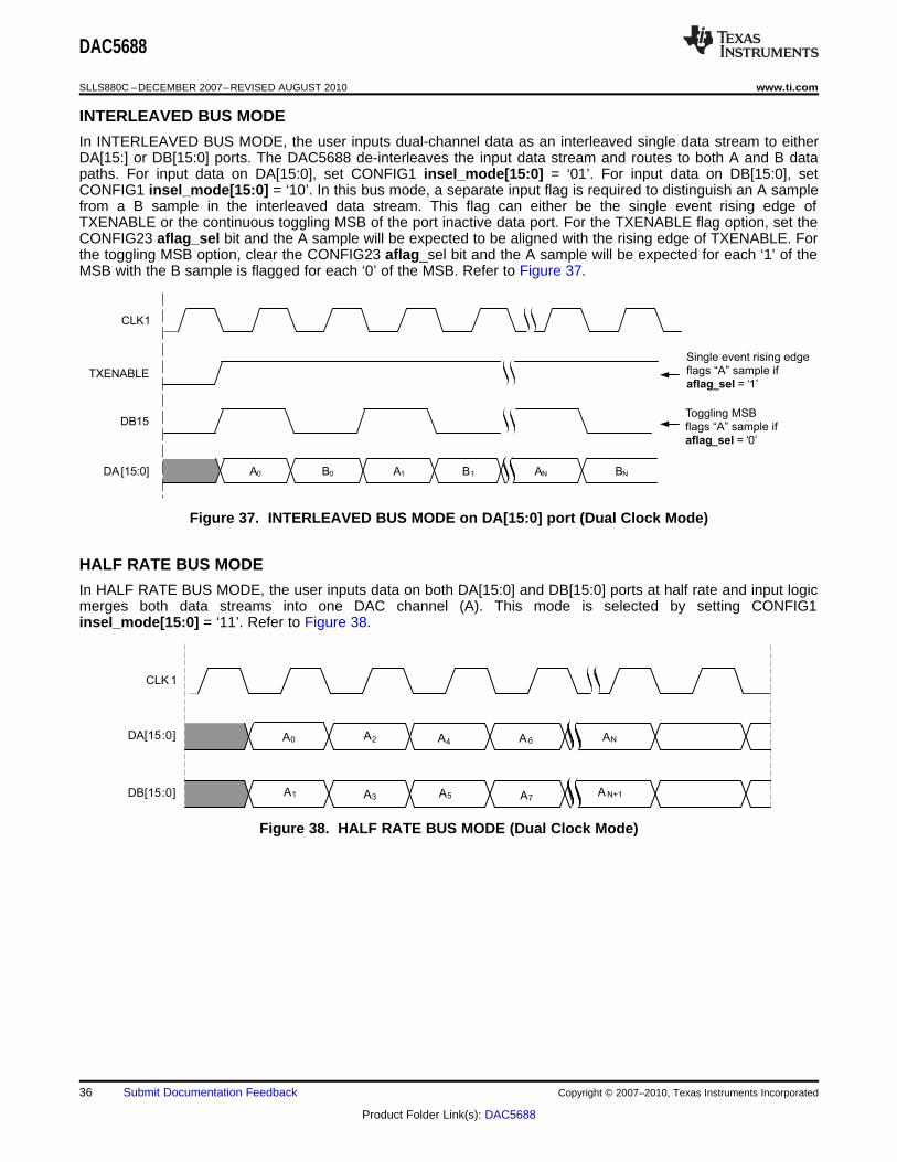
INTERLEAVED BUS MODE
In INTERLEAVED BUS MODE, the user inputs dual-channel data as an interleaved single data stream to eitherDA[15:] or DB[15:0] ports. The DAC5688 de-interleaves the input data stream and routes to both A and B datapaths. For input data on DA[15:0], set CONFIG1 insel_mode[15:0] = ‘01’. For input data on DB[15:0], setCONFIG1 insel_mode[15:0] = ‘10’. In this bus mode, a separate input flag is required to distinguish an A samplefrom a B sample in the interleaved data stream. This flag can either be the single event rising edge ofTXENABLE or the continuous toggling MSB of the port inactive data port. For the TXENABLE flag option, set theCONFIG23 aflag_sel bit and the A sample will be expected to be aligned with the rising edge of TXENABLE. Forthe toggling MSB option, clear the CONFIG23 aflag_sel bit and the A sample will be expected for each ‘1’ of theMSB with the B sample is flagged for each ‘0’ of the MSB. Refer to Figure 37.
Figure 37. INTERLEAVED BUS MODE on DA[15:0] port (Dual Clock Mode)
HALF RATE BUS MODE
In HALF RATE BUS MODE, the user inputs data on both DA[15:0] and DB[15:0] ports at half rate and input logicmerges both data streams into one DAC channel (A). This mode is selected by setting CONFIG1insel_mode[15:0] = ‘11’. Refer to Figure 38.
Figure 38. HALF RATE BUS MODE (Dual Clock Mode)
36 Submit Documentation Feedback Copyright © 2007–2010, Texas Instruments Incorporated
Product Folder Link(s): DAC5688

CLK2
CLK2C666 W
333 W
Note: Input common mode level isapproximately 2/3 * CLKVDD or 1.2 V.
GND
CLKVDD
2 KW
2 KW
0.1 mF
CLK 2
CLK2C
0.1 mF
C AC
DifferentialECL
or (LV)PECLSource
+
-
RT150 W
100 W
150 W
DAC5688
www.ti.com SLLS880C –DECEMBER 2007–REVISED AUGUST 2010
CLK2 and CLK2C Inputs
Figure 39 shows an equivalent circuit for the DAC input clock (CLK2/C).
Figure 39. CLK2/C Equivalent Input Circuit
Figure 40 shows the preferred configuration for driving the CLK2/CLK2C input clock with a differential ECL/PECLsource.
Figure 40. Preferred Clock Input Configuration With a Differential ECL/PECL Clock Source
Copyright © 2007–2010, Texas Instruments Incorporated Submit Documentation Feedback 37
Product Folder Link(s): DAC5688

CLKO _CLK1
LOCK _CLK1C
diffclk_ena
EN
clk1c_in_ena
EN
1
0
clk1_in_ena
Internal CLK1
Internal LOCK
Internal CLKOEN
clko_SE_hold
GND
GND
IOVDD
IOVDD
GND
IOVDD
GND
IOVDD
CLKO _CLK1
LOCK _CLK1C
10 KW
Note: Input common mode level isapproximately 0.5* IOVDD or 1.65 V.
10 KW
10 KW
10 KW
DAC5688
SLLS880C –DECEMBER 2007–REVISED AUGUST 2010 www.ti.com
CLKO_CLK1 and LOCK_CLK1C Pins
Figure 41 shows the functionality of the CLKO_CLK1 and LOCK_CLK1C pins. Refer to Table 5. The controls forthese pins are found in the CONFIG2 register and are used in selection of device clocking mode. In single-endedmode (CONFIG2 diffclk_ena = ‘0’) refer to Figure 43, both CLKO_CLK1 and LOCK_CLK1C pins have aninternal pull-down resistor approximately equivalent to 100kΩ.
Figure 41. CLKO_CLK1 and LOCK_CLK1C pins bi-directional control
In differential mode (CONFIG2 diffclk_ena = ‘1’) the CLKO_CLK1 and LOCK_CLK1C input pins are configuredas a differential CLK1/C clock input. Refer Figure 39 for the equivalent circuit.
Figure 42. CLKO_CLK1 and LOCK_CLK1C Differential Input Mode Equivalent Circuit
38 Submit Documentation Feedback Copyright © 2007–2010, Texas Instruments Incorporated
Product Folder Link(s): DAC5688

400 W
SCLK
SYNC
TXENABLE
DA[15:0]
DB[15:0]
CLKO _CLK 1**
** As an input
Internal
digital in
IOVDD
GND
RESETB
SDENB
Internal
digital in
IOVDD
100 k
W
100 k
W
GND
400 W
DAC5688
www.ti.com SLLS880C –DECEMBER 2007–REVISED AUGUST 2010
CMOS DIGITAL INPUTS
Figure 43 shows a schematic of the equivalent CMOS digital inputs of the DAC5688. SDIO, SCLK, SYNC,TXENABLE, DA[15:0] and DB[15:0] have pull-down resistors while RESETB and SDENB have pull-up resistorsinternal the DAC5688. See specification table for logic thresholds. The pull-up and pull-down circuitry isapproximately equivalent to 100kΩ.
The input switches levels for all CMOS digital inputs can be changed from 3.3V input levels to 1.8V input leversby programming the CONFIG26 io_1p8_3p3 register bit. If io_1p8_3p3 is cleared, the input thresholds are setfor 3.3V CMOS levels. If io_1p8_3p3 is set, the input thresholds are set for 1.8V levels.
Figure 43. CMOS/TTL Digital Equivalent Input
REFERENCE OPERATION
The DAC5688 uses a bandgap reference and control amplifier for biasing the full-scale output current. Thefull-scale output current is set by applying an external resistor RBIAS to pin BIASJ. The bias current IBIAS throughresistor RBIAS is defined by the on-chip bandgap reference voltage and control amplifier. The default full-scaleoutput current equals 16 times this bias current and can thus be expressed as:
IOUTFS = 16 × IBIAS = 16 × VEXTIO / RBIAS
Each DAC has a 4-bit independent coarse gain control via coarse_daca(3:0) and coarse_dacb (3:0) in theCONFIG27 register. Using gain control, the IOUTFS can be expressed as:
IOUTAFS = (DACA_gain + 1) × IBIAS = (DACA_gain + 1) × VEXTIO / RBIAS
IOUTBFS = (DACB_gain + 1) × IBIAS = (DACB_gain + 1) × VEXTIO / RBIAS
where VEXTIO is the voltage at terminal EXTIO. The bandgap reference voltage delivers an accurate voltage of1.2 V. This reference is active when terminal EXTLO is connected to AGND. An external decoupling capacitorCEXT of 0.1 mF should be connected externally to terminal EXTIO for compensation. The bandgap reference canadditionally be used for external reference operation. In that case, an external buffer with high impedance inputshould be applied in order to limit the bandgap load current to a maximum of 100 nA. The internal reference canbe disabled and overridden by an external reference by connecting EXTLO to AVDD. Capacitor CEXT may hencebe omitted. Terminal EXTIO thus serves as either input or output node.
The full-scale output current can be adjusted from 20 mA down to 2 mA by varying resistor RBIAS or changing theexternally applied reference voltage. The internal control amplifier has a wide input range, supporting thefull-scale output current range of 20 dB.
DAC TRANSFER FUNCTION
The CMOS DAC’s consist of a segmented array of NMOS current sinks, capable of sinking a full-scale outputcurrent up to 20 mA. Differential current switches direct the current to either one of the complementary outputnodes IOUT1 or IOUT2. (DACA = IOUTA1 or IOUTA2 and DACB = IOUTB1 or IOUTB2.) Complementary outputcurrents enable differential operation, thus canceling out common mode noise sources (digital feed-through,on-chip and PCB noise), dc offsets, even order distortion components, and increasing signal output power by afactor of two.
Copyright © 2007–2010, Texas Instruments Incorporated Submit Documentation Feedback 39
Product Folder Link(s): DAC5688

DAC5688
SLLS880C –DECEMBER 2007–REVISED AUGUST 2010 www.ti.com
The full-scale output current is set using external resistor RBIAS in combination with an on-chip bandgap voltagereference source (+1.2 V) and control amplifier. Current IBIAS through resistor RBIAS is mirrored internally toprovide a maximum full-scale output current equal to 16 times IBIAS.
The relation between IOUT1 and IOUT2 can be expressed as:IOUT1 = – IOUTFS – IOUT2
We will denote current flowing into a node as – current and current flowing out of a node as + current. Since theoutput stage is a current sink the current can only flow from AVDD into the IOUT1 and IOUT2 pins. The outputcurrent flow in each pin driving a resistive load can be expressed as:
IOUT1 = IOUTFS × (65536 – CODE) / 65536IOUT2 = IOUTFS × CODE / 65536
where CODE is the decimal representation of the DAC data input word.
For the case where IOUT1 and IOUT2 drive resistor loads RL directly, this translates into single ended voltagesat IOUT1 and IOUT2:
VOUT1 = AVDD – | IOUT1 | × RL
VOUT2 = AVDD – | IOUT2 | × RL
Assuming that the data is full scale (65536 in offset binary notation) and the RL is 25 Ω, the differential voltagebetween pins IOUT1 and IOUT2 can be expressed as:
VOUT1 = AVDD – | –0mA | × 25 Ω = 3.3 VVOUT2 = AVDD – | –20mA | × 25 Ω = 2.8 VVDIFF = VOUT1 – VOUT2 = 0.5V
Note that care should be taken not to exceed the compliance voltages at node IOUT1 and IOUT2, which wouldlead to increased signal distortion.
DAC OUTPUT SINC RESPONSE
Due to sampled nature of a high-speed DAC’s, the well known sin(x)/x (or SINC) response can significantlyattenuate higher frequency output signals. Refer to Figure 44 which shows the unitized SINC attenuation roll-offwith respect to the final DAC sample rate in 4 Nyquist zones. For example, if the final DAC sample rate FS = 1.0GSPS, then a tone at 440MHz will be attenuated by 3.0dB. Although the SINC response can create challengesin frequency planning, one side benefit is the natural attenuation of Nyquist images. The increased over-samplingratio of the input data provided by the DAC5688’s 2x, 4x and 8x digital interpolation modes improve the SINCroll-off (droop) within the original signal’s band of interest.
Figure 44. Unitized DAC sin(x)/x (SINC) Response
40 Submit Documentation Feedback Copyright © 2007–2010, Texas Instruments Incorporated
Product Folder Link(s): DAC5688

RLOAD
AVDD
S(1)
S(1)C
S(2)
S(2)C
S(N)
S(N)C
...
IOUT1 IOUT2
RLOAD
DAC5688
www.ti.com SLLS880C –DECEMBER 2007–REVISED AUGUST 2010
ANALOG CURRENT OUTPUTS
Figure 45 shows a simplified schematic of the current source array output with corresponding switches.Differential switches direct the current of each individual NMOS current source to either the positive output nodeIOUT1 or its complementary negative output node IOUT2. The output impedance is determined by the stack ofthe current sources and differential switches, and is typically >300 kΩ in parallel with an output capacitance of 5pF.
The external output resistors are referred to an external ground. The minimum output compliance at nodesIOUT1 and IOUT2 is limited to AVDD – 0.5 V, determined by the CMOS process. Beyond this value, transistorbreakdown may occur resulting in reduced reliability of the DAC5688 device. The maximum output compliancevoltage at nodes IOUT1 and IOUT2 equals AVDD + 0.5 V. Exceeding the minimum output compliance voltageadversely affects distortion performance and integral non-linearity. The optimum distortion performance for asingle-ended or differential output is achieved when the maximum full-scale signal at IOUT1 and IOUT2 does notexceed 0.5 V.
Figure 45. Equivalent Analog Current Output
The DAC5688 can be easily configured to drive a doubly terminated 50Ω cable using a properly selected RFtransformer. Figure 46 and Figure 47 show the 50Ω doubly terminated transformer configuration with 1:1 and 4:1impedance ratio, respectively. Note that the center tap of the primary input of the transformer has to beconnected to AVDD to enable a cd current flow. Applying a 20mA full-scale output current would lead to a 0.5VPP for a 1:1 transformer and a 1 VPP output for a 4:1 transformer. The low dc-impedance between IOUT1 orIOUT2 and the transformer center tap sets the center of the ac-signal at AVDD, so the 1 VPP output for the 4:1transformer results in an output between AVDD + 0.5 V and AVDD – 0.5 V.
Copyright © 2007–2010, Texas Instruments Incorporated Submit Documentation Feedback 41
Product Folder Link(s): DAC5688

IOUT11:1
IOUT 2
RLOAD
100 W
50 W
AVDD (3.3 V)
AVDD (3.3 V)
50 W
50 W
IOUT 1 4:1
50 W
RLOAD
100 W
IOUT 2
AVDD (3.3 V)
AVDD (3.3 V)
100 W
DAC5688
SLLS880C –DECEMBER 2007–REVISED AUGUST 2010 www.ti.com
Figure 46. Driving a Doubly Terminated 50Ω Cable Using a 1:1 Impedance Ratio Transformer
Figure 47. Driving a Doubly Terminated 50Ω Cable Using a 4:1 Impedance Ratio Transformer
PASSIVE INTERFACE TO ANALOG QUADRATURE MODULATORS
A common application in communication systems is to interface the DAC to an IQ modulator like the TRF3703family of modulators from Texas Instruments. The input of the modulator is generally of high impedance andrequires a specific common-mode voltage. A simple resistive network can be used to maintain 50Ω loadimpedance for the DAC5688 and also provide the necessary common-mode voltages for both the DAC and themodulator.
42 Submit Documentation Feedback Copyright © 2007–2010, Texas Instruments Incorporated
Product Folder Link(s): DAC5688

IOUTA1
IOUTA2
IOUTB1
IOUTB2
S
RF
Sig
na
lC
on
dit
ion
ing
Quadrature modulator
Vout ~ 2.8 to 3.8 V Vin ~ Varies
I1
I2
Q1
Q2
I
/I
TRF3703-17
I
/I
V1
V1
R1
R1
R2
R2R3
R3
V2DAC5688
DAC5688
www.ti.com SLLS880C –DECEMBER 2007–REVISED AUGUST 2010
Figure 48. DAC to Analog Quadrature Modulator Interface
The DAC5688 has a maximum 20mA full-scale output and a voltage compliance range of AVDD ± 0.5 V. TheTRF3703 IQ modulator family can be operated at three common-mode voltages: 1.5V, 1.7V, and 3.3V.
Figure 49 shows the recommended passive network to interface the DAC5688 to the TRF3703-17 which has acommon mode voltage of 1.7V. The network generates the 3.3V common mode required by the DAC output and1.7V at the modulator input, while still maintaining 50Ω load for the DAC.
Figure 49. DAC5688 to TRF3703-17 Interface
If V1 is set to 5V and V2 is set to -5V, the corresponding resistor values are R1 = 57Ω, R2 = 80Ω, and R3 =336Ω. The loss developed through R2 is about -1.86 dB. In the case where there is no –5V supply available andV2 is set to 0V, the resistor values are R1 = 66Ω, R2 = 101Ω, and R3 = 107Ω. The loss with these values is–5.76dB.
Figure 50 shows the recommended network for interfacing with the TRF3703-33 which requires a common modeof 3.3V. This is the simplest interface as there is no voltage shift. Because there is no voltage shift there is anyloss in the network. With V1 = 5V and V2 = 0V, the resistor values are R1 = 66Ω and R3 = 208Ω.
Copyright © 2007–2010, Texas Instruments Incorporated Submit Documentation Feedback 43
Product Folder Link(s): DAC5688

I
/I
TRF3703-33
I
/I
V1
V1
R1
R1
R3
R3
V2DAC5688
DAC5688
I
/I
TRF3703
V1
R1
R1
R3
R3
Filter R4
V1
R2
R2
V2
DAC5688
SLLS880C –DECEMBER 2007–REVISED AUGUST 2010 www.ti.com
Figure 50. DAC5688 to TRF3703-33 Interface
In most applications a baseband filter is required between the DAC and the modulator to eliminate the DACimages. This filter can be placed after the common-mode biasing network. For the DAC to modulator networkshown in Figure 51, R2 and the filter load R4 need to be considered into the DAC impedance. The filter has to bedesigned for the source impedance created by the resistor combination of R3 // (R2+R1). The effectiveimpedance seen by the DAC is affected by the filter termination resistor resulting in R1 // (R2+R3 // (R4/2)).
Figure 51. DAC5688 to Modulator Interface with Filter
Factoring in R4 into the DAC load, a typical interface to the TRF3703-17 with V1 = 5V and V2 = 0V results in thefollowing values: R1 = 72Ω, R2 = 116Ω, R3 = 124Ω and R4 = 150Ω. This implies that the filter needs to bedesigned for 75Ω input and output impedance (single-ended impedance). The common mode levels for the DACand modulator are maintained at 3.3V and 1.7V and the DAC load is 50Ω. The added load of the filtertermination causes the signal to be attenuated by –10.8 dB.
A filter can be implemented in a similar manner to interface with the TRF3703-33. In this case it is much simplerto balance the loads and common mode voltages due to the absence of R2. An added benefit is that there is noloss in this network. With V1 = 5V and V2 = 0V the network can be designed such that R1 = 115Ω, R3 = 681Ω,and R4 = 200Ω. This results in a filter impedance of R1 // R2=100Ω, and a DAC load of R1 // R3 // (R4/2) whichis equal to 50Ω. R4 is a differential resistor and does not affect the common mode level created by R1 and R3.The common-mode voltage is set at 3.3 V for a full-scale current of 20mA.
For more information on how to interface the DAC5688 to an analog quadrature modulator please refer to theapplication reports Passive Terminations for Current Output DACs (SLAA399) and Design of Differential Filtersfor High-Speed Signal Chains (SLWA053).
44 Submit Documentation Feedback Copyright © 2007–2010, Texas Instruments Incorporated
Product Folder Link(s): DAC5688

C1 11 23 C2
1 23
R1 32
1(3 2)
1
KdKvco
2d
tand secd 2
1dtand secd
3
tand secdd
DAC5688
www.ti.com SLLS880C –DECEMBER 2007–REVISED AUGUST 2010
RECOMMENDED STARTUP SEQUENCE
The following startup sequence is recommend to initialization the DAC5688:1. Supply all 1.8V (CLKVDD, DVDD, VFUSE) and 3.3V (AVDD and IOVDD) voltages.2. Toggle RESETB pin for a minimum 25 nSec active low pulse width.3. Provide a stable CLK2/C input clock.4. Program all desired SIF registers.5. Provide a sync signal to all digital blocks. The sync input source may be either TXENABLE pin, SYNC pin or
a software sync via CONFIG5 sif_sync_sig bit; however, only the TXENABLE or SYNC pins arerecommended for multi-DAC synchronization. Refer to CONFIG5, CONFIG22 and CONFIG23 registers forsync source selection. Note: Registers CONFIG6 through CONFIG13 all require a sync input to transfer thecontents of the control register inputs to the active digital blocks.
6. Provide data flow.
MULTI-DAC SYNCHRONIZATION
If the system has two or more DACs requiring synchronization, the sync signal in Step 5 of the RECOMMENDEDSTARTUP SEQUENCE must be provided to all the DACs simultaneously. The sync input source must be eitherthe TXENABLE pin or the SYNC pin (the software sync is not recommended).
In some applications such as beamforming it is required that the multiple DACs in the system have constantlatency thus resulting in phase aligned outputs. As a result of the clock domain transfer on the DAC5688 FIFO,the outputs of all DACs can only be synchronized to within ±1 DAC clock cycle in the External and Dual Clockmodes. In order to guarantee exact phase alignment between all devices it is required to set up the device inDual Synchronous Clock mode.
DESIGNING THE PLL LOOP FILTER
To minimize phase noise given for a given fDAC and M/N, the values of PLL_gain and PLL_range are selectedso that GVCO is minimized and within the MIN and MAX frequency for a given setting.
The external loop filter components C1, C2, and R1 are set by the GVCO, M/N, the loop phase margin fd and theloop bandwidth wd. Except for applications where abrupt clock frequency changes require a fast PLL lock time, itis suggested that fd be set to at least 80 degrees for stable locking and suppression of the phase noise sidelobes. Phase margins of 60 degrees or less can be sensitive to board layout and decoupling details.
See Figure 52 for the recommend external loop filter topology. C1, C2, and R1 are calculated by the followingequations
(5)
where
(6)
charge pump current: Iqp = 1 mAvco gain: KVCO = 2p × GVCO rad/VPFD Frequency: wd ≤ 160 MHzphase detector gain: Kd = Iqp ÷ (2 × p × M) A/rad
Copyright © 2007–2010, Texas Instruments Incorporated Submit Documentation Feedback 45
Product Folder Link(s): DAC5688

PLL External
LoopFilter
LPFPin 64
DAC5688 PLL
C 2 C 1
R 1
DAC5688
SLLS880C –DECEMBER 2007–REVISED AUGUST 2010 www.ti.com
An Excel spreadsheet is provided by Texas Instruments for automatically calculating the values for C1, R1 andC2.
Figure 52. Recommended External Loop Filter Topology
46 Submit Documentation Feedback Copyright © 2007–2010, Texas Instruments Incorporated
Product Folder Link(s): DAC5688

DAC5688
www.ti.com SLLS880C –DECEMBER 2007–REVISED AUGUST 2010
REVISION HISTORY
NOTE: Page numbers of previous versions may differ from current version.
Changes from Revision A (March 2008) to Revision B Page
• Changed Dual-Channel to first of title ................................................................................................................................... 1
• Changed sin(x)/x from upper case to lower case ................................................................................................................. 1
• Added sentence to DESCRIPTION section.."The DAC5688....multiplying PLL." ................................................................. 1
• Changed to join last column 2 bottom rows as one .............................................................................................................. 1
• Deleted "and External" from description of pin 25 ................................................................................................................ 3
• Added sentence to description of pin 1 ................................................................................................................................ 3
• Added sentence to description of pin 10,39,50,63 ............................................................................................................... 3
• Added text to description of TXENABLE, pin 6 .................................................................................................................... 3
• Deleted part of condition - Measured differential....to AVDD ................................................................................................ 5
• Changed min value from 1.71 to 1.7, max value from 2.15 to 1.9 ....................................................................................... 5
• Deleted min value -0.2 and max value 0.2, and added typ value of +/-0.2 .......................................................................... 5
• Deleted "PLL = off" from 7 rows of Digital Latency description ............................................................................................ 6
• Changed test conditions "NCO off" to "NCO on"; last row of Digital Latency, 2 places ....................................................... 6
• Changed test conditions "NCO off" to "NCO" on next to last row of Digital Latency; and "QMC off" to "QMC on" ............. 6
• Deleted min value -40 and max value 40 and added +/-20 to typ value in IIH row ............................................................. 7
• Deleted min value -40 and max value 40 and added +/-20 to typ value in IIL row .............................................................. 7
• Deleted 0.22xIOVDD from max value and added 0.5 in row of VOL ................................................................................... 7
• Added 2 notes to EC digital specifications table .................................................................................................................. 7
• Changed sentence in Offset Error: under TEST METHODOLOGY ................................................................................... 14
• Added new register map table under REGISTER DESCRIPTIONS section ...................................................................... 15
• Changed text in Register STATUS0 ................................................................................................................................... 16
• Changed Bit 0 of Register CONFIG2 from 0 to 1 ............................................................................................................... 17
• Changed text of Register CONFIG3 description ................................................................................................................ 17
• Changed text of Register CONFIG4 description ................................................................................................................ 17
• Deleted "Reserved" explanation from Register CONFIG5 description. .............................................................................. 18
• Changed phaseoffset(15:0) to phaseoffset(15:8) in Register CONFIG7 description ......................................................... 18
• Changed "Phaseadd(31:0)" to "phaseadd(31:24)" in Register CONFIG11 description ..................................................... 19
• Deleted explanatory "Note" from Register CONFG14 description ..................................................................................... 20
• Added text to Register CONFIG20 description. .................................................................................................................. 21
• Added text to Register CONFIG21 description. .................................................................................................................. 21
• Changed "Default 0x00" to "Default 0x15" for Register CONFIG23 Address .................................................................... 22
• Changed text in Register CONFIG23 description ............................................................................................................... 22
• Changed Register CONFIG28 description from "Reserved(7:0)" to "cleared" ................................................................... 23
• Deleted "cleared" in description for Register CONFG28 .................................................................................................... 23
• Deleted explanatory NOTE from Register CONFIG30 description. .................................................................................... 24
• Added sentence to 1st paragraph of section "SERIAL INTERFACE" description. ............................................................. 25
• Changed graphic entity for Figure 22, Magnitude Spectrum for FIR1 ................................................................................ 28
• Changed text in section "Full Complex Mixer (FMIX)." ....................................................................................................... 31
• Changed QOUT equation in Full Complex Mixer (FMIX) section. ........................................................................................ 31
• Changed description for section "Quadrature Modulator Correction (QMC)." .................................................................... 32
• Changed description for section "DAC Offset Control." ...................................................................................................... 32
• Changed text in section "DUAL SYNCHRONOUS CLOCK MODE." ................................................................................. 33
• Added text in section "DUAL CLOCK MODE." ................................................................................................................... 33
Copyright © 2007–2010, Texas Instruments Incorporated Submit Documentation Feedback 47
Product Folder Link(s): DAC5688

DAC5688
SLLS880C –DECEMBER 2007–REVISED AUGUST 2010 www.ti.com
• Changed Figure 36 , Figure 37, Figure 38, caption from "......(PLL Clock Mode)" to "......(Dual Clock Mode)" ................. 35
• Changed graphic entity for Figure 40 ................................................................................................................................. 37
• Added section "PASSIVE INTERFACE TO ANALOG QUADRATURE MODULATORS." ................................................. 42
• Changed text in section "RECOMMENDED STARTUP SEQUENCE " ............................................................................. 45
Changes from Revision B (August 2010) to Revision C Page
• Changed cos in equation 2 to sin ....................................................................................................................................... 31
48 Submit Documentation Feedback Copyright © 2007–2010, Texas Instruments Incorporated
Product Folder Link(s): DAC5688

PACKAGE OPTION ADDENDUM
www.ti.com 24-Aug-2018
Addendum-Page 1
PACKAGING INFORMATION
Orderable Device Status(1)
Package Type PackageDrawing
Pins PackageQty
Eco Plan(2)
Lead/Ball Finish(6)
MSL Peak Temp(3)
Op Temp (°C) Device Marking(4/5)
Samples
DAC5688IRGCR ACTIVE VQFN RGC 64 2000 Green (RoHS& no Sb/Br)
CU NIPDAU Level-3-260C-168 HR -40 to 85 DAC5688I
DAC5688IRGCT ACTIVE VQFN RGC 64 250 Green (RoHS& no Sb/Br)
CU NIPDAU Level-3-260C-168 HR -40 to 85 DAC5688I
(1) The marketing status values are defined as follows:ACTIVE: Product device recommended for new designs.LIFEBUY: TI has announced that the device will be discontinued, and a lifetime-buy period is in effect.NRND: Not recommended for new designs. Device is in production to support existing customers, but TI does not recommend using this part in a new design.PREVIEW: Device has been announced but is not in production. Samples may or may not be available.OBSOLETE: TI has discontinued the production of the device.
(2) RoHS: TI defines "RoHS" to mean semiconductor products that are compliant with the current EU RoHS requirements for all 10 RoHS substances, including the requirement that RoHS substancedo not exceed 0.1% by weight in homogeneous materials. Where designed to be soldered at high temperatures, "RoHS" products are suitable for use in specified lead-free processes. TI mayreference these types of products as "Pb-Free".RoHS Exempt: TI defines "RoHS Exempt" to mean products that contain lead but are compliant with EU RoHS pursuant to a specific EU RoHS exemption.Green: TI defines "Green" to mean the content of Chlorine (Cl) and Bromine (Br) based flame retardants meet JS709B low halogen requirements of <=1000ppm threshold. Antimony trioxide basedflame retardants must also meet the <=1000ppm threshold requirement.
(3) MSL, Peak Temp. - The Moisture Sensitivity Level rating according to the JEDEC industry standard classifications, and peak solder temperature.
(4) There may be additional marking, which relates to the logo, the lot trace code information, or the environmental category on the device.
(5) Multiple Device Markings will be inside parentheses. Only one Device Marking contained in parentheses and separated by a "~" will appear on a device. If a line is indented then it is a continuationof the previous line and the two combined represent the entire Device Marking for that device.
(6) Lead/Ball Finish - Orderable Devices may have multiple material finish options. Finish options are separated by a vertical ruled line. Lead/Ball Finish values may wrap to two lines if the finishvalue exceeds the maximum column width.
Important Information and Disclaimer:The information provided on this page represents TI's knowledge and belief as of the date that it is provided. TI bases its knowledge and belief on informationprovided by third parties, and makes no representation or warranty as to the accuracy of such information. Efforts are underway to better integrate information from third parties. TI has taken andcontinues to take reasonable steps to provide representative and accurate information but may not have conducted destructive testing or chemical analysis on incoming materials and chemicals.TI and TI suppliers consider certain information to be proprietary, and thus CAS numbers and other limited information may not be available for release.
In no event shall TI's liability arising out of such information exceed the total purchase price of the TI part(s) at issue in this document sold by TI to Customer on an annual basis.
PACKAGE OPTION ADDENDUM
www.ti.com 24-Aug-2018
Addendum-Page 2

TAPE AND REEL INFORMATION
*All dimensions are nominal
Device PackageType
PackageDrawing
Pins SPQ ReelDiameter
(mm)
ReelWidth
W1 (mm)
A0(mm)
B0(mm)
K0(mm)
P1(mm)
W(mm)
Pin1Quadrant
DAC5688IRGCR VQFN RGC 64 2000 330.0 16.4 9.3 9.3 1.5 12.0 16.0 Q2
DAC5688IRGCT VQFN RGC 64 250 330.0 16.4 9.3 9.3 1.5 12.0 16.0 Q2
PACKAGE MATERIALS INFORMATION
www.ti.com 9-Aug-2017
Pack Materials-Page 1

*All dimensions are nominal
Device Package Type Package Drawing Pins SPQ Length (mm) Width (mm) Height (mm)
DAC5688IRGCR VQFN RGC 64 2000 367.0 367.0 38.0
DAC5688IRGCT VQFN RGC 64 250 367.0 367.0 38.0
PACKAGE MATERIALS INFORMATION
www.ti.com 9-Aug-2017
Pack Materials-Page 2


IMPORTANT NOTICE
Texas Instruments Incorporated (TI) reserves the right to make corrections, enhancements, improvements and other changes to itssemiconductor products and services per JESD46, latest issue, and to discontinue any product or service per JESD48, latest issue. Buyersshould obtain the latest relevant information before placing orders and should verify that such information is current and complete.TI’s published terms of sale for semiconductor products (http://www.ti.com/sc/docs/stdterms.htm) apply to the sale of packaged integratedcircuit products that TI has qualified and released to market. Additional terms may apply to the use or sale of other types of TI products andservices.Reproduction of significant portions of TI information in TI data sheets is permissible only if reproduction is without alteration and isaccompanied by all associated warranties, conditions, limitations, and notices. TI is not responsible or liable for such reproduceddocumentation. Information of third parties may be subject to additional restrictions. Resale of TI products or services with statementsdifferent from or beyond the parameters stated by TI for that product or service voids all express and any implied warranties for theassociated TI product or service and is an unfair and deceptive business practice. TI is not responsible or liable for any such statements.Buyers and others who are developing systems that incorporate TI products (collectively, “Designers”) understand and agree that Designersremain responsible for using their independent analysis, evaluation and judgment in designing their applications and that Designers havefull and exclusive responsibility to assure the safety of Designers' applications and compliance of their applications (and of all TI productsused in or for Designers’ applications) with all applicable regulations, laws and other applicable requirements. Designer represents that, withrespect to their applications, Designer has all the necessary expertise to create and implement safeguards that (1) anticipate dangerousconsequences of failures, (2) monitor failures and their consequences, and (3) lessen the likelihood of failures that might cause harm andtake appropriate actions. Designer agrees that prior to using or distributing any applications that include TI products, Designer willthoroughly test such applications and the functionality of such TI products as used in such applications.TI’s provision of technical, application or other design advice, quality characterization, reliability data or other services or information,including, but not limited to, reference designs and materials relating to evaluation modules, (collectively, “TI Resources”) are intended toassist designers who are developing applications that incorporate TI products; by downloading, accessing or using TI Resources in anyway, Designer (individually or, if Designer is acting on behalf of a company, Designer’s company) agrees to use any particular TI Resourcesolely for this purpose and subject to the terms of this Notice.TI’s provision of TI Resources does not expand or otherwise alter TI’s applicable published warranties or warranty disclaimers for TIproducts, and no additional obligations or liabilities arise from TI providing such TI Resources. TI reserves the right to make corrections,enhancements, improvements and other changes to its TI Resources. TI has not conducted any testing other than that specificallydescribed in the published documentation for a particular TI Resource.Designer is authorized to use, copy and modify any individual TI Resource only in connection with the development of applications thatinclude the TI product(s) identified in such TI Resource. NO OTHER LICENSE, EXPRESS OR IMPLIED, BY ESTOPPEL OR OTHERWISETO ANY OTHER TI INTELLECTUAL PROPERTY RIGHT, AND NO LICENSE TO ANY TECHNOLOGY OR INTELLECTUAL PROPERTYRIGHT OF TI OR ANY THIRD PARTY IS GRANTED HEREIN, including but not limited to any patent right, copyright, mask work right, orother intellectual property right relating to any combination, machine, or process in which TI products or services are used. Informationregarding or referencing third-party products or services does not constitute a license to use such products or services, or a warranty orendorsement thereof. Use of TI Resources may require a license from a third party under the patents or other intellectual property of thethird party, or a license from TI under the patents or other intellectual property of TI.TI RESOURCES ARE PROVIDED “AS IS” AND WITH ALL FAULTS. TI DISCLAIMS ALL OTHER WARRANTIES ORREPRESENTATIONS, EXPRESS OR IMPLIED, REGARDING RESOURCES OR USE THEREOF, INCLUDING BUT NOT LIMITED TOACCURACY OR COMPLETENESS, TITLE, ANY EPIDEMIC FAILURE WARRANTY AND ANY IMPLIED WARRANTIES OFMERCHANTABILITY, FITNESS FOR A PARTICULAR PURPOSE, AND NON-INFRINGEMENT OF ANY THIRD PARTY INTELLECTUALPROPERTY RIGHTS. TI SHALL NOT BE LIABLE FOR AND SHALL NOT DEFEND OR INDEMNIFY DESIGNER AGAINST ANY CLAIM,INCLUDING BUT NOT LIMITED TO ANY INFRINGEMENT CLAIM THAT RELATES TO OR IS BASED ON ANY COMBINATION OFPRODUCTS EVEN IF DESCRIBED IN TI RESOURCES OR OTHERWISE. IN NO EVENT SHALL TI BE LIABLE FOR ANY ACTUAL,DIRECT, SPECIAL, COLLATERAL, INDIRECT, PUNITIVE, INCIDENTAL, CONSEQUENTIAL OR EXEMPLARY DAMAGES INCONNECTION WITH OR ARISING OUT OF TI RESOURCES OR USE THEREOF, AND REGARDLESS OF WHETHER TI HAS BEENADVISED OF THE POSSIBILITY OF SUCH DAMAGES.Unless TI has explicitly designated an individual product as meeting the requirements of a particular industry standard (e.g., ISO/TS 16949and ISO 26262), TI is not responsible for any failure to meet such industry standard requirements.Where TI specifically promotes products as facilitating functional safety or as compliant with industry functional safety standards, suchproducts are intended to help enable customers to design and create their own applications that meet applicable functional safety standardsand requirements. Using products in an application does not by itself establish any safety features in the application. Designers mustensure compliance with safety-related requirements and standards applicable to their applications. Designer may not use any TI products inlife-critical medical equipment unless authorized officers of the parties have executed a special contract specifically governing such use.Life-critical medical equipment is medical equipment where failure of such equipment would cause serious bodily injury or death (e.g., lifesupport, pacemakers, defibrillators, heart pumps, neurostimulators, and implantables). Such equipment includes, without limitation, allmedical devices identified by the U.S. Food and Drug Administration as Class III devices and equivalent classifications outside the U.S.TI may expressly designate certain products as completing a particular qualification (e.g., Q100, Military Grade, or Enhanced Product).Designers agree that it has the necessary expertise to select the product with the appropriate qualification designation for their applicationsand that proper product selection is at Designers’ own risk. Designers are solely responsible for compliance with all legal and regulatoryrequirements in connection with such selection.Designer will fully indemnify TI and its representatives against any damages, costs, losses, and/or liabilities arising out of Designer’s non-compliance with the terms and provisions of this Notice.
Mailing Address: Texas Instruments, Post Office Box 655303, Dallas, Texas 75265Copyright © 2018, Texas Instruments Incorporated