dsp56800erm, dsp56800e and dsp56800ex - reference manual · digital signal controller cores...
TRANSCRIPT

Digital Signal ControllerCores
freescale.com
DSP56800E and DSP56800EXReference Manual
DSP56800ERMRev. 309/2011


Contents
About This Book
Audience . . . . . . . . . . . . . . . . . . . . . . . . . . . . . . . . . . . . . . . . . . . . . . . . . . . . . . . . . . . xxviiOrganization . . . . . . . . . . . . . . . . . . . . . . . . . . . . . . . . . . . . . . . . . . . . . . . . . . . . . . . . xxviiSuggested Reading . . . . . . . . . . . . . . . . . . . . . . . . . . . . . . . . . . . . . . . . . . . . . . . . . . . xxviiiConventions . . . . . . . . . . . . . . . . . . . . . . . . . . . . . . . . . . . . . . . . . . . . . . . . . . . . . . . . . xxixDefinitions, Acronyms, and Abbreviations . . . . . . . . . . . . . . . . . . . . . . . . . . . . . . . . . . xxx
Chapter 1Introduction
1.1 Key Features . . . . . . . . . . . . . . . . . . . . . . . . . . . . . . . . . . . . . . . . . . . . . . . . . . . . . . . . . . 1-11.2 Architectural Overview. . . . . . . . . . . . . . . . . . . . . . . . . . . . . . . . . . . . . . . . . . . . . . . . . . 1-31.3 Example DSP56800EX Device . . . . . . . . . . . . . . . . . . . . . . . . . . . . . . . . . . . . . . . . . . . 1-41.4 Introduction to Digital Signal Processing. . . . . . . . . . . . . . . . . . . . . . . . . . . . . . . . . . . . 1-5
Chapter 2Core Architecture Overview
2.1 Extending DSP56800E Architecture . . . . . . . . . . . . . . . . . . . . . . . . . . . . . . . . . . . . . . . 2-12.2 Extending DSP56800 Architecture. . . . . . . . . . . . . . . . . . . . . . . . . . . . . . . . . . . . . . . . . 2-12.3 Core Programming Model . . . . . . . . . . . . . . . . . . . . . . . . . . . . . . . . . . . . . . . . . . . . . . . 2-22.4 Dual Harvard Memory Architecture. . . . . . . . . . . . . . . . . . . . . . . . . . . . . . . . . . . . . . . . 2-52.5 System Architecture and Peripheral Interface . . . . . . . . . . . . . . . . . . . . . . . . . . . . . . . . 2-62.5.1 Core Block Diagram . . . . . . . . . . . . . . . . . . . . . . . . . . . . . . . . . . . . . . . . . . . . . . . . . 2-72.5.2 Address Buses. . . . . . . . . . . . . . . . . . . . . . . . . . . . . . . . . . . . . . . . . . . . . . . . . . . . . . 2-82.5.3 Data Buses . . . . . . . . . . . . . . . . . . . . . . . . . . . . . . . . . . . . . . . . . . . . . . . . . . . . . . . . 2-82.5.4 Data Arithmetic Logic Unit (ALU) . . . . . . . . . . . . . . . . . . . . . . . . . . . . . . . . . . . . . 2-92.5.5 Address Generation Unit (AGU) . . . . . . . . . . . . . . . . . . . . . . . . . . . . . . . . . . . . . . . 2-92.5.6 Program Controller and Hardware Looping Unit . . . . . . . . . . . . . . . . . . . . . . . . . . 2-102.5.7 Bit-Manipulation Unit. . . . . . . . . . . . . . . . . . . . . . . . . . . . . . . . . . . . . . . . . . . . . . . 2-112.5.8 Enhanced On-Chip Emulation (Enhanced OnCE) Unit . . . . . . . . . . . . . . . . . . . . . 2-112.6 Blocks Outside the Core . . . . . . . . . . . . . . . . . . . . . . . . . . . . . . . . . . . . . . . . . . . . . . . . 2-112.6.1 Program Memory . . . . . . . . . . . . . . . . . . . . . . . . . . . . . . . . . . . . . . . . . . . . . . . . . . 2-112.6.2 Data Memory . . . . . . . . . . . . . . . . . . . . . . . . . . . . . . . . . . . . . . . . . . . . . . . . . . . . . 2-112.6.3 Bootstrap Memory . . . . . . . . . . . . . . . . . . . . . . . . . . . . . . . . . . . . . . . . . . . . . . . . . 2-122.6.4 External Bus Interface . . . . . . . . . . . . . . . . . . . . . . . . . . . . . . . . . . . . . . . . . . . . . . 2-12
Chapter 3Data Types and Addressing Modes
3.1 Core Programming Model . . . . . . . . . . . . . . . . . . . . . . . . . . . . . . . . . . . . . . . . . . . . . . . 3-1
Freescale Semiconductor Table of Contents iii

3.2 Data Types . . . . . . . . . . . . . . . . . . . . . . . . . . . . . . . . . . . . . . . . . . . . . . . . . . . . . . . . . . . 3-53.2.1 Data Formats. . . . . . . . . . . . . . . . . . . . . . . . . . . . . . . . . . . . . . . . . . . . . . . . . . . . . . . 3-63.2.1.1 Signed Integer . . . . . . . . . . . . . . . . . . . . . . . . . . . . . . . . . . . . . . . . . . . . . . . . . . . 3-63.2.1.2 Unsigned Integer. . . . . . . . . . . . . . . . . . . . . . . . . . . . . . . . . . . . . . . . . . . . . . . . . 3-63.2.1.3 Signed Fractional . . . . . . . . . . . . . . . . . . . . . . . . . . . . . . . . . . . . . . . . . . . . . . . . 3-63.2.1.4 Unsigned Fractional . . . . . . . . . . . . . . . . . . . . . . . . . . . . . . . . . . . . . . . . . . . . . . 3-73.2.2 Understanding Fractional and Integer Data . . . . . . . . . . . . . . . . . . . . . . . . . . . . . . . 3-73.3 Memory Access Overview . . . . . . . . . . . . . . . . . . . . . . . . . . . . . . . . . . . . . . . . . . . . . . . 3-83.3.1 Move Instruction Syntax. . . . . . . . . . . . . . . . . . . . . . . . . . . . . . . . . . . . . . . . . . . . . . 3-83.3.1.1 Ordering Source and Destination . . . . . . . . . . . . . . . . . . . . . . . . . . . . . . . . . . . . 3-93.3.1.2 Memory Space Syntax . . . . . . . . . . . . . . . . . . . . . . . . . . . . . . . . . . . . . . . . . . . . 3-93.3.1.3 Specifying Data Size. . . . . . . . . . . . . . . . . . . . . . . . . . . . . . . . . . . . . . . . . . . . . . 3-93.3.2 Instructions That Access Data Memory . . . . . . . . . . . . . . . . . . . . . . . . . . . . . . . . . . 3-93.3.2.1 Signed and Unsigned Moves . . . . . . . . . . . . . . . . . . . . . . . . . . . . . . . . . . . . . . . 3-93.3.2.2 Moving Words from Memory to a Register . . . . . . . . . . . . . . . . . . . . . . . . . . . 3-103.3.2.3 Accessing Peripheral Registers. . . . . . . . . . . . . . . . . . . . . . . . . . . . . . . . . . . . . 3-103.3.3 Instructions That Access Program Memory . . . . . . . . . . . . . . . . . . . . . . . . . . . . . . 3-113.3.4 Instructions with an Operand in Data Memory . . . . . . . . . . . . . . . . . . . . . . . . . . . 3-113.3.5 Parallel Moves . . . . . . . . . . . . . . . . . . . . . . . . . . . . . . . . . . . . . . . . . . . . . . . . . . . . 3-113.3.5.1 Single Parallel Move. . . . . . . . . . . . . . . . . . . . . . . . . . . . . . . . . . . . . . . . . . . . . 3-123.3.5.2 Dual Parallel Read . . . . . . . . . . . . . . . . . . . . . . . . . . . . . . . . . . . . . . . . . . . . . . 3-123.4 Data Alignment. . . . . . . . . . . . . . . . . . . . . . . . . . . . . . . . . . . . . . . . . . . . . . . . . . . . . . . 3-133.4.1 Data Alignment in Accumulators . . . . . . . . . . . . . . . . . . . . . . . . . . . . . . . . . . . . . . 3-133.4.2 Data Alignment in Data Registers . . . . . . . . . . . . . . . . . . . . . . . . . . . . . . . . . . . . . 3-143.4.3 Data Alignment in 24-Bit AGU and Control Registers . . . . . . . . . . . . . . . . . . . . . 3-143.4.4 Data Alignment in 16-Bit AGU and Control Registers . . . . . . . . . . . . . . . . . . . . . 3-153.4.5 Data Alignment in Memory . . . . . . . . . . . . . . . . . . . . . . . . . . . . . . . . . . . . . . . . . . 3-153.4.5.1 Byte and Word Addresses. . . . . . . . . . . . . . . . . . . . . . . . . . . . . . . . . . . . . . . . . 3-163.4.5.2 Byte Variable Alignment . . . . . . . . . . . . . . . . . . . . . . . . . . . . . . . . . . . . . . . . . 3-163.4.5.3 Word Variable Alignment . . . . . . . . . . . . . . . . . . . . . . . . . . . . . . . . . . . . . . . . 3-173.4.5.4 Long-Word Alignment . . . . . . . . . . . . . . . . . . . . . . . . . . . . . . . . . . . . . . . . . . . 3-173.5 Memory Access and Pointers . . . . . . . . . . . . . . . . . . . . . . . . . . . . . . . . . . . . . . . . . . . . 3-173.5.1 Word and Byte Pointers . . . . . . . . . . . . . . . . . . . . . . . . . . . . . . . . . . . . . . . . . . . . . 3-173.5.2 Accessing Word Values Using Word Pointers . . . . . . . . . . . . . . . . . . . . . . . . . . . . 3-193.5.3 Accessing Long-Word Values Using Word Pointers . . . . . . . . . . . . . . . . . . . . . . . 3-193.5.4 Accessing Byte Values Using Word Pointers. . . . . . . . . . . . . . . . . . . . . . . . . . . . . 3-213.5.5 Accessing Byte Values Using Byte Pointers . . . . . . . . . . . . . . . . . . . . . . . . . . . . . 3-213.6 Addressing Modes . . . . . . . . . . . . . . . . . . . . . . . . . . . . . . . . . . . . . . . . . . . . . . . . . . . . 3-233.6.1 Addressing Mode Summary . . . . . . . . . . . . . . . . . . . . . . . . . . . . . . . . . . . . . . . . . . 3-233.6.2 Register-Direct Modes . . . . . . . . . . . . . . . . . . . . . . . . . . . . . . . . . . . . . . . . . . . . . . 3-283.6.3 Address-Register-Indirect Modes . . . . . . . . . . . . . . . . . . . . . . . . . . . . . . . . . . . . . . 3-283.6.3.1 No Update: (Rn) . . . . . . . . . . . . . . . . . . . . . . . . . . . . . . . . . . . . . . . . . . . . . . . . 3-293.6.3.2 Post-Increment: (Rn)+ . . . . . . . . . . . . . . . . . . . . . . . . . . . . . . . . . . . . . . . . . . . 3-303.6.3.3 Post-Decrement: (Rn)– . . . . . . . . . . . . . . . . . . . . . . . . . . . . . . . . . . . . . . . . . . . 3-313.6.3.4 Post-Update by Offset N: (Rn)+N, (R3)+N3 . . . . . . . . . . . . . . . . . . . . . . . . . . 3-323.6.3.5 Index by Offset N: (Rn+N). . . . . . . . . . . . . . . . . . . . . . . . . . . . . . . . . . . . . . . . 3-333.6.3.6 Index by 3-Bit Displacement: (RRR+x), (SP–x) . . . . . . . . . . . . . . . . . . . . . . . 3-34
iv DSP56800E and DSP56800EX Core Reference Manual Freescale Semiconductor

3.6.3.7 Index by 6-Bit Displacement: (SP–xx) . . . . . . . . . . . . . . . . . . . . . . . . . . . . . . . 3-353.6.3.8 Index by 16-Bit Displacement: (Rn+xxxx) . . . . . . . . . . . . . . . . . . . . . . . . . . . 3-363.6.3.9 Index by 24-Bit Displacement: (Rn+xxxxxx) . . . . . . . . . . . . . . . . . . . . . . . . . 3-373.6.4 Immediate Address Modes . . . . . . . . . . . . . . . . . . . . . . . . . . . . . . . . . . . . . . . . . . . 3-383.6.4.1 4-Bit Immediate Data: #x . . . . . . . . . . . . . . . . . . . . . . . . . . . . . . . . . . . . . . . . . 3-383.6.4.2 5-Bit Immediate Data: #xx . . . . . . . . . . . . . . . . . . . . . . . . . . . . . . . . . . . . . . . . 3-383.6.4.3 6-Bit Immediate Data: #xx . . . . . . . . . . . . . . . . . . . . . . . . . . . . . . . . . . . . . . . . 3-383.6.4.4 7-Bit Immediate Data: #xx . . . . . . . . . . . . . . . . . . . . . . . . . . . . . . . . . . . . . . . . 3-393.6.4.5 16-Bit Immediate Data: #xxxx . . . . . . . . . . . . . . . . . . . . . . . . . . . . . . . . . . . . . 3-393.6.4.6 32-Bit Immediate Data: #xxxxxxxx . . . . . . . . . . . . . . . . . . . . . . . . . . . . . . . . . 3-413.6.5 Absolute Address Modes . . . . . . . . . . . . . . . . . . . . . . . . . . . . . . . . . . . . . . . . . . . . 3-413.6.5.1 Absolute Short Address: aa. . . . . . . . . . . . . . . . . . . . . . . . . . . . . . . . . . . . . . . . 3-423.6.5.2 I/O Short Address: <<pp. . . . . . . . . . . . . . . . . . . . . . . . . . . . . . . . . . . . . . . . . . 3-433.6.5.3 16-Bit Absolute Address: xxxx. . . . . . . . . . . . . . . . . . . . . . . . . . . . . . . . . . . . . 3-443.6.5.4 24-Bit Absolute Address: xxxxxx. . . . . . . . . . . . . . . . . . . . . . . . . . . . . . . . . . . 3-453.6.6 Implicit Address Modes . . . . . . . . . . . . . . . . . . . . . . . . . . . . . . . . . . . . . . . . . . . . . 3-453.6.7 Bit-Reverse Address Mode (DSP56800EX Core only) . . . . . . . . . . . . . . . . . . . . . 3-45
Chapter 4Instruction Set Introduction
4.1 Instruction Groups . . . . . . . . . . . . . . . . . . . . . . . . . . . . . . . . . . . . . . . . . . . . . . . . . . . . . 4-14.1.1 Multiplication Instructions . . . . . . . . . . . . . . . . . . . . . . . . . . . . . . . . . . . . . . . . . . . . 4-24.1.2 Arithmetic Instructions . . . . . . . . . . . . . . . . . . . . . . . . . . . . . . . . . . . . . . . . . . . . . . . 4-34.1.3 Shifting Instructions . . . . . . . . . . . . . . . . . . . . . . . . . . . . . . . . . . . . . . . . . . . . . . . . . 4-64.1.4 Logical Instructions . . . . . . . . . . . . . . . . . . . . . . . . . . . . . . . . . . . . . . . . . . . . . . . . . 4-74.1.5 AGU Arithmetic Instructions . . . . . . . . . . . . . . . . . . . . . . . . . . . . . . . . . . . . . . . . . . 4-74.1.6 Bit-Manipulation Instructions. . . . . . . . . . . . . . . . . . . . . . . . . . . . . . . . . . . . . . . . . . 4-94.1.7 Looping Instructions . . . . . . . . . . . . . . . . . . . . . . . . . . . . . . . . . . . . . . . . . . . . . . . . . 4-94.1.8 Move Instructions . . . . . . . . . . . . . . . . . . . . . . . . . . . . . . . . . . . . . . . . . . . . . . . . . . 4-104.1.9 Program Control Instructions . . . . . . . . . . . . . . . . . . . . . . . . . . . . . . . . . . . . . . . . . 4-104.2 Instruction Aliases . . . . . . . . . . . . . . . . . . . . . . . . . . . . . . . . . . . . . . . . . . . . . . . . . . . . 4-124.2.1 The ANDC, EORC, ORC, and NOTC Aliases. . . . . . . . . . . . . . . . . . . . . . . . . . . . 4-124.2.2 Instruction Operand Remapping. . . . . . . . . . . . . . . . . . . . . . . . . . . . . . . . . . . . . . . 4-134.2.2.1 Duplicate Operand Remapping. . . . . . . . . . . . . . . . . . . . . . . . . . . . . . . . . . . . . 4-134.2.2.2 Addressing Mode Remapping . . . . . . . . . . . . . . . . . . . . . . . . . . . . . . . . . . . . . 4-134.3 Delayed Flow Control Instructions. . . . . . . . . . . . . . . . . . . . . . . . . . . . . . . . . . . . . . . . 4-144.3.1 Using Delayed Instructions. . . . . . . . . . . . . . . . . . . . . . . . . . . . . . . . . . . . . . . . . . . 4-144.3.2 Delayed Instruction Restrictions. . . . . . . . . . . . . . . . . . . . . . . . . . . . . . . . . . . . . . . 4-154.3.3 Delayed Instructions and Interrupts . . . . . . . . . . . . . . . . . . . . . . . . . . . . . . . . . . . . 4-164.4 Instruction Set Summary . . . . . . . . . . . . . . . . . . . . . . . . . . . . . . . . . . . . . . . . . . . . . . . 4-164.4.1 Using the Instruction Summary Tables . . . . . . . . . . . . . . . . . . . . . . . . . . . . . . . . . 4-164.4.2 Register Field Notation. . . . . . . . . . . . . . . . . . . . . . . . . . . . . . . . . . . . . . . . . . . . . . 4-174.4.3 Immediate Value Notation . . . . . . . . . . . . . . . . . . . . . . . . . . . . . . . . . . . . . . . . . . . 4-214.4.4 Instruction Summary Tables . . . . . . . . . . . . . . . . . . . . . . . . . . . . . . . . . . . . . . . . . . 4-214.4.5 Parallel Move Summary Tables . . . . . . . . . . . . . . . . . . . . . . . . . . . . . . . . . . . . . . . 4-494.5 Register-to-Register Moves . . . . . . . . . . . . . . . . . . . . . . . . . . . . . . . . . . . . . . . . . . . . . 4-51
Freescale Semiconductor Table of Contents v

Chapter 5Data Arithmetic Logic Unit
5.1 Data ALU Overview and Architecture . . . . . . . . . . . . . . . . . . . . . . . . . . . . . . . . . . . . . . 5-25.1.1 Data Registers (X0, Y1, Y0). . . . . . . . . . . . . . . . . . . . . . . . . . . . . . . . . . . . . . . . . . . 5-35.1.2 Accumulator Registers (A, B, C, D) . . . . . . . . . . . . . . . . . . . . . . . . . . . . . . . . . . . . . 5-45.1.3 Multiply-Accumulator (MAC) and Logic Unit . . . . . . . . . . . . . . . . . . . . . . . . . . . . 5-55.1.4 Single-Bit Accumulator Shifter . . . . . . . . . . . . . . . . . . . . . . . . . . . . . . . . . . . . . . . . 5-55.1.5 Arithmetic and Logical Shifter . . . . . . . . . . . . . . . . . . . . . . . . . . . . . . . . . . . . . . . . . 5-65.1.6 Data Limiter and MAC Output Limiter . . . . . . . . . . . . . . . . . . . . . . . . . . . . . . . . . . 5-65.2 Accessing the Accumulator Registers . . . . . . . . . . . . . . . . . . . . . . . . . . . . . . . . . . . . . . 5-65.2.1 Accessing an Entire Accumulator. . . . . . . . . . . . . . . . . . . . . . . . . . . . . . . . . . . . . . . 5-85.2.1.1 Writing an Accumulator with a Small Operand . . . . . . . . . . . . . . . . . . . . . . . . . 5-85.2.1.2 Using the Extension Registers . . . . . . . . . . . . . . . . . . . . . . . . . . . . . . . . . . . . . . 5-95.2.2 Accessing Portions of an Accumulator. . . . . . . . . . . . . . . . . . . . . . . . . . . . . . . . . . . 5-95.2.3 Reading and Writing Integer Data to an Accumulator . . . . . . . . . . . . . . . . . . . . . . 5-125.2.4 Reading 16-Bit Results of DSC Algorithms. . . . . . . . . . . . . . . . . . . . . . . . . . . . . . 5-125.2.5 Converting a 36-Bit Accumulator to a 16-Bit Value . . . . . . . . . . . . . . . . . . . . . . . 5-135.2.6 Saving and Restoring Accumulators. . . . . . . . . . . . . . . . . . . . . . . . . . . . . . . . . . . . 5-135.2.7 Bit-Manipulation Operations on Accumulators . . . . . . . . . . . . . . . . . . . . . . . . . . . 5-145.3 Fractional and Integer Arithmetic. . . . . . . . . . . . . . . . . . . . . . . . . . . . . . . . . . . . . . . . . 5-145.3.1 DSP56800E Data Types . . . . . . . . . . . . . . . . . . . . . . . . . . . . . . . . . . . . . . . . . . . . . 5-155.3.2 Addition and Subtraction . . . . . . . . . . . . . . . . . . . . . . . . . . . . . . . . . . . . . . . . . . . . 5-165.3.3 Multiplication . . . . . . . . . . . . . . . . . . . . . . . . . . . . . . . . . . . . . . . . . . . . . . . . . . . . . 5-185.3.3.1 Fractional Multiplication . . . . . . . . . . . . . . . . . . . . . . . . . . . . . . . . . . . . . . . . . 5-185.3.3.2 Integer Multiplication . . . . . . . . . . . . . . . . . . . . . . . . . . . . . . . . . . . . . . . . . . . . 5-195.3.3.3 Operand Re-Ordering for Multiplication Instructions . . . . . . . . . . . . . . . . . . . 5-205.3.4 Division. . . . . . . . . . . . . . . . . . . . . . . . . . . . . . . . . . . . . . . . . . . . . . . . . . . . . . . . . . 5-215.3.4.1 General-Purpose Four-Quadrant Division . . . . . . . . . . . . . . . . . . . . . . . . . . . . 5-225.3.4.2 Positive Dividend and Divisor with Remainder . . . . . . . . . . . . . . . . . . . . . . . . 5-235.3.4.3 Signed Dividend and Divisor with No Remainder . . . . . . . . . . . . . . . . . . . . . . 5-235.3.4.4 Division Overflow . . . . . . . . . . . . . . . . . . . . . . . . . . . . . . . . . . . . . . . . . . . . . . 5-245.3.5 Logical Operations . . . . . . . . . . . . . . . . . . . . . . . . . . . . . . . . . . . . . . . . . . . . . . . . . 5-255.3.6 Shifting Operations . . . . . . . . . . . . . . . . . . . . . . . . . . . . . . . . . . . . . . . . . . . . . . . . . 5-255.3.6.1 Shifting 16-Bit Words. . . . . . . . . . . . . . . . . . . . . . . . . . . . . . . . . . . . . . . . . . . . 5-255.3.6.2 Shifting 32-Bit Long Words . . . . . . . . . . . . . . . . . . . . . . . . . . . . . . . . . . . . . . . 5-265.3.6.3 Shifting Accumulators by 16 Bits. . . . . . . . . . . . . . . . . . . . . . . . . . . . . . . . . . . 5-275.3.6.4 Shifting with Accumulation . . . . . . . . . . . . . . . . . . . . . . . . . . . . . . . . . . . . . . . 5-275.4 Unsigned Arithmetic Operations . . . . . . . . . . . . . . . . . . . . . . . . . . . . . . . . . . . . . . . . . 5-275.4.1 Condition Codes for Unsigned Operations . . . . . . . . . . . . . . . . . . . . . . . . . . . . . . . 5-275.4.2 Unsigned Single-Precision Multiplication . . . . . . . . . . . . . . . . . . . . . . . . . . . . . . . 5-285.5 Extended- and Multi-Precision Operations. . . . . . . . . . . . . . . . . . . . . . . . . . . . . . . . . . 5-295.5.1 Extended-Precision Addition and Subtraction . . . . . . . . . . . . . . . . . . . . . . . . . . . . 5-295.5.2 Multi-Precision Fractional Multiplication . . . . . . . . . . . . . . . . . . . . . . . . . . . . . . . 5-295.5.3 Multi-Precision Integer Multiplication . . . . . . . . . . . . . . . . . . . . . . . . . . . . . . . . . . 5-325.5.3.1 Signed 32-Bit × Signed 32-Bit with 32-Bit Result . . . . . . . . . . . . . . . . . . . . . . 5-335.5.3.2 Unsigned 32-Bit × Unsigned 32-Bit with 32-Bit Result. . . . . . . . . . . . . . . . . . 5-345.5.3.3 Signed 32-Bit × Signed 32-Bit with 64-Bit Result . . . . . . . . . . . . . . . . . . . . . . 5-34
vi DSP56800E and DSP56800EX Core Reference Manual Freescale Semiconductor

5.5.3.4 Other Applications of Multi-Precision Integer Multiplication . . . . . . . . . . . . . 5-355.6 Normalizing . . . . . . . . . . . . . . . . . . . . . . . . . . . . . . . . . . . . . . . . . . . . . . . . . . . . . . . . . 5-365.6.1 Normalized Values . . . . . . . . . . . . . . . . . . . . . . . . . . . . . . . . . . . . . . . . . . . . . . . . . 5-365.6.2 Normalizing Methods . . . . . . . . . . . . . . . . . . . . . . . . . . . . . . . . . . . . . . . . . . . . . . . 5-375.7 Condition Code Calculation . . . . . . . . . . . . . . . . . . . . . . . . . . . . . . . . . . . . . . . . . . . . . 5-385.7.1 Condition Code Modes . . . . . . . . . . . . . . . . . . . . . . . . . . . . . . . . . . . . . . . . . . . . . . 5-385.7.2 Condition Codes and Data Sizes. . . . . . . . . . . . . . . . . . . . . . . . . . . . . . . . . . . . . . . 5-385.8 Saturation and Data Limiting . . . . . . . . . . . . . . . . . . . . . . . . . . . . . . . . . . . . . . . . . . . . 5-395.8.1 Data Limiter . . . . . . . . . . . . . . . . . . . . . . . . . . . . . . . . . . . . . . . . . . . . . . . . . . . . . . 5-395.8.2 MAC Output Limiter . . . . . . . . . . . . . . . . . . . . . . . . . . . . . . . . . . . . . . . . . . . . . . . 5-415.8.3 Instructions Not Affected by the MAC Output Limiter . . . . . . . . . . . . . . . . . . . . . 5-425.9 Rounding. . . . . . . . . . . . . . . . . . . . . . . . . . . . . . . . . . . . . . . . . . . . . . . . . . . . . . . . . . . . 5-435.9.1 Convergent Rounding . . . . . . . . . . . . . . . . . . . . . . . . . . . . . . . . . . . . . . . . . . . . . . . 5-445.9.2 Two’s-Complement Rounding . . . . . . . . . . . . . . . . . . . . . . . . . . . . . . . . . . . . . . . . 5-465.9.3 Rounding Examples . . . . . . . . . . . . . . . . . . . . . . . . . . . . . . . . . . . . . . . . . . . . . . . . 5-46
Chapter 6Address Generation Unit
6.1 AGU Architecture. . . . . . . . . . . . . . . . . . . . . . . . . . . . . . . . . . . . . . . . . . . . . . . . . . . . . . 6-16.1.1 Primary Address Arithmetic Unit . . . . . . . . . . . . . . . . . . . . . . . . . . . . . . . . . . . . . . . 6-26.1.2 Secondary Address Adder Unit . . . . . . . . . . . . . . . . . . . . . . . . . . . . . . . . . . . . . . . . 6-36.1.3 Single-Bit Shifting Units . . . . . . . . . . . . . . . . . . . . . . . . . . . . . . . . . . . . . . . . . . . . . 6-36.2 AGU Programming Model . . . . . . . . . . . . . . . . . . . . . . . . . . . . . . . . . . . . . . . . . . . . . . . 6-36.2.1 Address Registers (R0–R5, N) . . . . . . . . . . . . . . . . . . . . . . . . . . . . . . . . . . . . . . . . . 6-46.2.2 Stack Pointer Register (SP). . . . . . . . . . . . . . . . . . . . . . . . . . . . . . . . . . . . . . . . . . . . 6-46.2.3 Offset Register (N) . . . . . . . . . . . . . . . . . . . . . . . . . . . . . . . . . . . . . . . . . . . . . . . . . . 6-56.2.4 Secondary Read Offset Register (N3) . . . . . . . . . . . . . . . . . . . . . . . . . . . . . . . . . . . 6-56.2.5 Modifier Register (M01). . . . . . . . . . . . . . . . . . . . . . . . . . . . . . . . . . . . . . . . . . . . . . 6-56.2.6 Shadow Registers . . . . . . . . . . . . . . . . . . . . . . . . . . . . . . . . . . . . . . . . . . . . . . . . . . . 6-56.3 Using Address Registers . . . . . . . . . . . . . . . . . . . . . . . . . . . . . . . . . . . . . . . . . . . . . . . . . 6-66.4 Byte and Word Addresses. . . . . . . . . . . . . . . . . . . . . . . . . . . . . . . . . . . . . . . . . . . . . . . . 6-76.5 Word Pointer Memory Accesses . . . . . . . . . . . . . . . . . . . . . . . . . . . . . . . . . . . . . . . . . . 6-86.5.1 Accessing Bytes . . . . . . . . . . . . . . . . . . . . . . . . . . . . . . . . . . . . . . . . . . . . . . . . . . . 6-106.5.2 Accessing Long Words . . . . . . . . . . . . . . . . . . . . . . . . . . . . . . . . . . . . . . . . . . . . . . 6-106.5.3 Accessing Data Structures . . . . . . . . . . . . . . . . . . . . . . . . . . . . . . . . . . . . . . . . . . . 6-116.5.4 Accessing Program Memory . . . . . . . . . . . . . . . . . . . . . . . . . . . . . . . . . . . . . . . . . 6-136.6 Byte Pointer Memory Accesses . . . . . . . . . . . . . . . . . . . . . . . . . . . . . . . . . . . . . . . . . . 6-136.6.1 Byte Pointers vs. Word Pointers . . . . . . . . . . . . . . . . . . . . . . . . . . . . . . . . . . . . . . . 6-146.6.2 Byte Arrays . . . . . . . . . . . . . . . . . . . . . . . . . . . . . . . . . . . . . . . . . . . . . . . . . . . . . . . 6-156.7 AGU Arithmetic Instructions . . . . . . . . . . . . . . . . . . . . . . . . . . . . . . . . . . . . . . . . . . . . 6-186.8 Linear and Modulo Address Arithmetic . . . . . . . . . . . . . . . . . . . . . . . . . . . . . . . . . . . . 6-206.8.1 Linear Address Arithmetic . . . . . . . . . . . . . . . . . . . . . . . . . . . . . . . . . . . . . . . . . . . 6-206.8.2 Understanding Modulo Arithmetic . . . . . . . . . . . . . . . . . . . . . . . . . . . . . . . . . . . . . 6-206.8.3 Configuring Modulo Arithmetic . . . . . . . . . . . . . . . . . . . . . . . . . . . . . . . . . . . . . . . 6-226.8.3.1 Configuring for Byte and Word Accesses . . . . . . . . . . . . . . . . . . . . . . . . . . . . 6-226.8.3.2 Configuring for Long Word Accesses . . . . . . . . . . . . . . . . . . . . . . . . . . . . . . . 6-236.8.4 Base Pointer and Offset Values in Modulo Instructions. . . . . . . . . . . . . . . . . . . . . 6-26
Freescale Semiconductor Table of Contents vii

6.8.4.1 Operand Placement Table . . . . . . . . . . . . . . . . . . . . . . . . . . . . . . . . . . . . . . . . . 6-266.8.4.2 Example of Incorrect Modulo Operation . . . . . . . . . . . . . . . . . . . . . . . . . . . . . 6-276.8.4.3 Special Case - ADDA Instructions in Modulo Arithmetic . . . . . . . . . . . . . . . . 6-286.8.4.3.1 Case 1. Adding a Positive Immediate Offset to a Pointer . . . . . . . . . . . . . 6-286.8.4.3.2 Case 2. Adding a Negative Immediate Offset to a Pointer . . . . . . . . . . . . . 6-286.8.4.4 Restrictions on the Offset Values . . . . . . . . . . . . . . . . . . . . . . . . . . . . . . . . . . . 6-286.8.5 Supported Memory Access Instructions . . . . . . . . . . . . . . . . . . . . . . . . . . . . . . . . . 6-296.8.5.1 Modulo Addressing for Word Memory Accesses . . . . . . . . . . . . . . . . . . . . . . 6-296.8.5.2 Modulo Addressing for Byte and Long Memory Accesses . . . . . . . . . . . . . . . 6-296.8.5.3 Modulo Addressing for AGU Arithmetic Instructions . . . . . . . . . . . . . . . . . . . 6-306.8.6 Simple Circular Buffer Example . . . . . . . . . . . . . . . . . . . . . . . . . . . . . . . . . . . . . . 6-306.8.7 Setting Up a Modulo Buffer . . . . . . . . . . . . . . . . . . . . . . . . . . . . . . . . . . . . . . . . . . 6-326.8.8 Wrapping to a Different Bank . . . . . . . . . . . . . . . . . . . . . . . . . . . . . . . . . . . . . . . . 6-336.8.9 Side Effects of Modulo Arithmetic. . . . . . . . . . . . . . . . . . . . . . . . . . . . . . . . . . . . . 6-346.8.9.1 When a Pointer Lies Outside a Modulo Buffer . . . . . . . . . . . . . . . . . . . . . . . . 6-346.8.9.2 Restrictions on the Offset Register . . . . . . . . . . . . . . . . . . . . . . . . . . . . . . . . . . 6-346.8.9.3 Memory Locations Not Accessible Using Modulo Arithmetic . . . . . . . . . . . . 6-34
Chapter 7Bit-Manipulation Unit
7.1 Bit-Manipulation Unit Overview and Architecture . . . . . . . . . . . . . . . . . . . . . . . . . . . . 7-27.1.1 8-Bit Mask Shift Unit . . . . . . . . . . . . . . . . . . . . . . . . . . . . . . . . . . . . . . . . . . . . . . . . 7-27.1.2 16-Bit Masking Logic . . . . . . . . . . . . . . . . . . . . . . . . . . . . . . . . . . . . . . . . . . . . . . . . 7-37.1.3 16-Bit Testing Logic . . . . . . . . . . . . . . . . . . . . . . . . . . . . . . . . . . . . . . . . . . . . . . . . . 7-37.1.4 16-Bit Logic Unit . . . . . . . . . . . . . . . . . . . . . . . . . . . . . . . . . . . . . . . . . . . . . . . . . . . 7-47.2 Bit-Manipulation Unit Operation . . . . . . . . . . . . . . . . . . . . . . . . . . . . . . . . . . . . . . . . . . 7-47.2.1 Testing Bits . . . . . . . . . . . . . . . . . . . . . . . . . . . . . . . . . . . . . . . . . . . . . . . . . . . . . . . . 7-47.2.2 Conditional Branching . . . . . . . . . . . . . . . . . . . . . . . . . . . . . . . . . . . . . . . . . . . . . . . 7-47.2.3 Modifying Selected Bits . . . . . . . . . . . . . . . . . . . . . . . . . . . . . . . . . . . . . . . . . . . . . . 7-57.3 ANDC, EORC, ORC, and NOTC. . . . . . . . . . . . . . . . . . . . . . . . . . . . . . . . . . . . . . . . . . 7-57.4 Other Bit-Manipulation Capabilities . . . . . . . . . . . . . . . . . . . . . . . . . . . . . . . . . . . . . . . 7-67.5 Programming Considerations . . . . . . . . . . . . . . . . . . . . . . . . . . . . . . . . . . . . . . . . . . . . . 7-67.5.1 Bit-Manipulation Operations on Registers . . . . . . . . . . . . . . . . . . . . . . . . . . . . . . . . 7-67.5.2 Bit-Manipulation Operations on Byte Values . . . . . . . . . . . . . . . . . . . . . . . . . . . . . 7-67.5.2.1 Absolute Addresses. . . . . . . . . . . . . . . . . . . . . . . . . . . . . . . . . . . . . . . . . . . . . . . 7-77.5.2.2 Word Pointers with Byte Offsets . . . . . . . . . . . . . . . . . . . . . . . . . . . . . . . . . . . . 7-77.5.3 Using Complex Addressing Modes . . . . . . . . . . . . . . . . . . . . . . . . . . . . . . . . . . . . . 7-87.5.4 Synthetic Conditional Branch and Jump Operations . . . . . . . . . . . . . . . . . . . . . . . . 7-87.5.4.1 JRSET and JRCLR Operations. . . . . . . . . . . . . . . . . . . . . . . . . . . . . . . . . . . . . . 7-97.5.4.2 BR1SET and BR1CLR Operations. . . . . . . . . . . . . . . . . . . . . . . . . . . . . . . . . . . 7-97.5.4.3 JR1SET and JR1CLR Operations. . . . . . . . . . . . . . . . . . . . . . . . . . . . . . . . . . . 7-10
Chapter 8Program Controller
8.1 Program Controller Architecture . . . . . . . . . . . . . . . . . . . . . . . . . . . . . . . . . . . . . . . . . . 8-18.1.1 Instruction Latch and Decoder . . . . . . . . . . . . . . . . . . . . . . . . . . . . . . . . . . . . . . . . . 8-2
viii DSP56800E and DSP56800EX Core Reference Manual Freescale Semiconductor

8.1.2 Program Counter. . . . . . . . . . . . . . . . . . . . . . . . . . . . . . . . . . . . . . . . . . . . . . . . . . . . 8-38.1.3 Looping Control Unit . . . . . . . . . . . . . . . . . . . . . . . . . . . . . . . . . . . . . . . . . . . . . . . . 8-38.1.4 Hardware Stack. . . . . . . . . . . . . . . . . . . . . . . . . . . . . . . . . . . . . . . . . . . . . . . . . . . . . 8-38.1.5 Interrupt Control Unit . . . . . . . . . . . . . . . . . . . . . . . . . . . . . . . . . . . . . . . . . . . . . . . . 8-38.1.6 Interrupt Controller . . . . . . . . . . . . . . . . . . . . . . . . . . . . . . . . . . . . . . . . . . . . . . . . . . 8-38.2 Program Controller Programming Model. . . . . . . . . . . . . . . . . . . . . . . . . . . . . . . . . . . . 8-48.2.1 Operating Mode Register . . . . . . . . . . . . . . . . . . . . . . . . . . . . . . . . . . . . . . . . . . . . . 8-48.2.1.1 Operating Mode (MA and MB)—Bits 0–1. . . . . . . . . . . . . . . . . . . . . . . . . . . . . 8-68.2.1.2 External X Memory (EX)—Bit 3 . . . . . . . . . . . . . . . . . . . . . . . . . . . . . . . . . . . . 8-68.2.1.3 Saturation (SA)—Bit 4 . . . . . . . . . . . . . . . . . . . . . . . . . . . . . . . . . . . . . . . . . . . . 8-68.2.1.4 Rounding (R)—Bit 5 . . . . . . . . . . . . . . . . . . . . . . . . . . . . . . . . . . . . . . . . . . . . . 8-68.2.1.5 Stop Delay (SD)—Bit 6 . . . . . . . . . . . . . . . . . . . . . . . . . . . . . . . . . . . . . . . . . . . 8-68.2.1.6 X or P Memory (XP)—Bit 7. . . . . . . . . . . . . . . . . . . . . . . . . . . . . . . . . . . . . . . . 8-68.2.1.7 Condition Code Mode (CM)—Bit 8 . . . . . . . . . . . . . . . . . . . . . . . . . . . . . . . . . . 8-78.2.1.8 Nested Looping (NL)—Bit 15 . . . . . . . . . . . . . . . . . . . . . . . . . . . . . . . . . . . . . . 8-78.2.2 Status Register . . . . . . . . . . . . . . . . . . . . . . . . . . . . . . . . . . . . . . . . . . . . . . . . . . . . . 8-78.2.2.1 Carry (C)—Bit 0 . . . . . . . . . . . . . . . . . . . . . . . . . . . . . . . . . . . . . . . . . . . . . . . . . 8-98.2.2.2 Overflow (V)—Bit 1. . . . . . . . . . . . . . . . . . . . . . . . . . . . . . . . . . . . . . . . . . . . . . 8-98.2.2.3 Zero (Z)—Bit 2 . . . . . . . . . . . . . . . . . . . . . . . . . . . . . . . . . . . . . . . . . . . . . . . . . . 8-98.2.2.4 Negative (N)—Bit 3 . . . . . . . . . . . . . . . . . . . . . . . . . . . . . . . . . . . . . . . . . . . . . . 8-98.2.2.5 Unnormalized (U)—Bit 4 . . . . . . . . . . . . . . . . . . . . . . . . . . . . . . . . . . . . . . . . . . 8-98.2.2.6 Extension in Use (E)—Bit 5 . . . . . . . . . . . . . . . . . . . . . . . . . . . . . . . . . . . . . . . 8-108.2.2.7 Limit (L)—Bit 6 . . . . . . . . . . . . . . . . . . . . . . . . . . . . . . . . . . . . . . . . . . . . . . . . 8-108.2.2.8 Size (SZ)—Bit 7 . . . . . . . . . . . . . . . . . . . . . . . . . . . . . . . . . . . . . . . . . . . . . . . . 8-108.2.2.9 Interrupt Mask (I0–I1)—Bits 8–9. . . . . . . . . . . . . . . . . . . . . . . . . . . . . . . . . . . 8-108.2.2.10 Program Counter Extension (P0–P4)—Bits 10–14 . . . . . . . . . . . . . . . . . . . . . 8-118.2.2.11 Loop Flag (LF)—Bit 15 . . . . . . . . . . . . . . . . . . . . . . . . . . . . . . . . . . . . . . . . . . 8-118.2.3 Loop Count Register . . . . . . . . . . . . . . . . . . . . . . . . . . . . . . . . . . . . . . . . . . . . . . . . 8-118.2.4 Loop Count Register 2 . . . . . . . . . . . . . . . . . . . . . . . . . . . . . . . . . . . . . . . . . . . . . . 8-118.2.5 Loop Address Register . . . . . . . . . . . . . . . . . . . . . . . . . . . . . . . . . . . . . . . . . . . . . . 8-128.2.6 Loop Address Register 2. . . . . . . . . . . . . . . . . . . . . . . . . . . . . . . . . . . . . . . . . . . . . 8-128.2.7 Hardware Stack Register . . . . . . . . . . . . . . . . . . . . . . . . . . . . . . . . . . . . . . . . . . . . 8-128.2.8 Fast Interrupt Status Register . . . . . . . . . . . . . . . . . . . . . . . . . . . . . . . . . . . . . . . . . 8-128.2.9 Fast Interrupt Return Address. . . . . . . . . . . . . . . . . . . . . . . . . . . . . . . . . . . . . . . . . 8-148.3 Software Stack . . . . . . . . . . . . . . . . . . . . . . . . . . . . . . . . . . . . . . . . . . . . . . . . . . . . . . . 8-148.3.1 Pushing and Popping Values . . . . . . . . . . . . . . . . . . . . . . . . . . . . . . . . . . . . . . . . . 8-148.3.2 Subroutines . . . . . . . . . . . . . . . . . . . . . . . . . . . . . . . . . . . . . . . . . . . . . . . . . . . . . . . 8-158.3.3 Interrupt Service Routines . . . . . . . . . . . . . . . . . . . . . . . . . . . . . . . . . . . . . . . . . . . 8-158.3.4 Parameter Passing and Local Variables . . . . . . . . . . . . . . . . . . . . . . . . . . . . . . . . . 8-168.4 Hardware Stack. . . . . . . . . . . . . . . . . . . . . . . . . . . . . . . . . . . . . . . . . . . . . . . . . . . . . . . 8-178.5 Hardware Looping . . . . . . . . . . . . . . . . . . . . . . . . . . . . . . . . . . . . . . . . . . . . . . . . . . . . 8-188.5.1 Repeat (REP) Looping . . . . . . . . . . . . . . . . . . . . . . . . . . . . . . . . . . . . . . . . . . . . . . 8-188.5.2 DO Looping . . . . . . . . . . . . . . . . . . . . . . . . . . . . . . . . . . . . . . . . . . . . . . . . . . . . . . 8-198.5.3 Specifying a Loop Count of Zero . . . . . . . . . . . . . . . . . . . . . . . . . . . . . . . . . . . . . . 8-208.5.4 Terminating a DO Loop . . . . . . . . . . . . . . . . . . . . . . . . . . . . . . . . . . . . . . . . . . . . . 8-208.5.4.1 Allowing Current Block to Finish and Then Exiting . . . . . . . . . . . . . . . . . . . . 8-208.5.4.2 Immediate Exit from a Hardware Loop . . . . . . . . . . . . . . . . . . . . . . . . . . . . . . 8-21
Freescale Semiconductor Table of Contents ix

8.5.5 Specifying a Large Immediate Loop Count . . . . . . . . . . . . . . . . . . . . . . . . . . . . . . 8-218.5.6 Nested Hardware Looping . . . . . . . . . . . . . . . . . . . . . . . . . . . . . . . . . . . . . . . . . . . 8-228.5.6.1 Nesting a REP Loop Within a DO Loop . . . . . . . . . . . . . . . . . . . . . . . . . . . . . 8-228.5.6.2 Nesting a DO Loop Within a DO Loop . . . . . . . . . . . . . . . . . . . . . . . . . . . . . . 8-228.5.6.3 Nesting a DO Loop Within a Software Loop . . . . . . . . . . . . . . . . . . . . . . . . . . 8-238.6 Executing Programs from Data Memory . . . . . . . . . . . . . . . . . . . . . . . . . . . . . . . . . . . 8-238.6.1 Entering Data-Memory Execution Mode . . . . . . . . . . . . . . . . . . . . . . . . . . . . . . . . 8-258.6.2 Exiting Data-Memory Execution Mode . . . . . . . . . . . . . . . . . . . . . . . . . . . . . . . . . 8-268.6.3 Interrupts in Data-Memory Execution Mode . . . . . . . . . . . . . . . . . . . . . . . . . . . . . 8-288.6.4 Restrictions on Data-Memory Execution Mode . . . . . . . . . . . . . . . . . . . . . . . . . . . 8-28
Chapter 9Processing States
9.1 Normal Processing State . . . . . . . . . . . . . . . . . . . . . . . . . . . . . . . . . . . . . . . . . . . . . . . . . 9-19.2 Reset Processing State . . . . . . . . . . . . . . . . . . . . . . . . . . . . . . . . . . . . . . . . . . . . . . . . . . 9-19.3 Exception Processing State . . . . . . . . . . . . . . . . . . . . . . . . . . . . . . . . . . . . . . . . . . . . . . . 9-29.3.1 Interrupt Priority Structure . . . . . . . . . . . . . . . . . . . . . . . . . . . . . . . . . . . . . . . . . . . . 9-39.3.2 Interrupt and Exception Processing . . . . . . . . . . . . . . . . . . . . . . . . . . . . . . . . . . . . . 9-49.3.2.1 Normal Interrupt Processing. . . . . . . . . . . . . . . . . . . . . . . . . . . . . . . . . . . . . . . . 9-59.3.2.2 Fast Interrupt Processing . . . . . . . . . . . . . . . . . . . . . . . . . . . . . . . . . . . . . . . . . . 9-69.3.3 Interrupt Sources. . . . . . . . . . . . . . . . . . . . . . . . . . . . . . . . . . . . . . . . . . . . . . . . . . . . 9-89.3.3.1 External Hardware Interrupt Sources . . . . . . . . . . . . . . . . . . . . . . . . . . . . . . . . . 9-89.3.3.2 Hardware Interrupt Sources Within the Core . . . . . . . . . . . . . . . . . . . . . . . . . . . 9-89.3.3.2.1 Illegal Instruction Interrupt . . . . . . . . . . . . . . . . . . . . . . . . . . . . . . . . . . . . . . 9-99.3.3.2.2 Hardware Stack Overflow Interrupt . . . . . . . . . . . . . . . . . . . . . . . . . . . . . . . 9-99.3.3.2.3 Misaligned Data Access Interrupt. . . . . . . . . . . . . . . . . . . . . . . . . . . . . . . . . 9-99.3.3.2.4 Debugging (Enhanced OnCE) Interrupts . . . . . . . . . . . . . . . . . . . . . . . . . . . 9-99.3.3.3 Software Interrupt Instructions . . . . . . . . . . . . . . . . . . . . . . . . . . . . . . . . . . . . . 9-109.3.3.3.1 SWI Instruction—Level 3. . . . . . . . . . . . . . . . . . . . . . . . . . . . . . . . . . . . . . 9-109.3.3.3.2 SWI #x Instructions—Levels 0–2. . . . . . . . . . . . . . . . . . . . . . . . . . . . . . . . 9-109.3.3.3.3 SWILP Instruction—Lowest Priority . . . . . . . . . . . . . . . . . . . . . . . . . . . . . 9-109.3.4 Non-Interruptible Instruction Sequences . . . . . . . . . . . . . . . . . . . . . . . . . . . . . . . . 9-109.4 Wait Processing State . . . . . . . . . . . . . . . . . . . . . . . . . . . . . . . . . . . . . . . . . . . . . . . . . . 9-119.4.1 Wait Mode Timing . . . . . . . . . . . . . . . . . . . . . . . . . . . . . . . . . . . . . . . . . . . . . . . . . 9-129.4.2 Disabling Wait Mode . . . . . . . . . . . . . . . . . . . . . . . . . . . . . . . . . . . . . . . . . . . . . . . 9-129.5 Stop Processing State . . . . . . . . . . . . . . . . . . . . . . . . . . . . . . . . . . . . . . . . . . . . . . . . . . 9-129.5.1 Stop Mode Timing . . . . . . . . . . . . . . . . . . . . . . . . . . . . . . . . . . . . . . . . . . . . . . . . . 9-139.5.2 Disabling Stop Mode . . . . . . . . . . . . . . . . . . . . . . . . . . . . . . . . . . . . . . . . . . . . . . . 9-139.6 Debug Processing State . . . . . . . . . . . . . . . . . . . . . . . . . . . . . . . . . . . . . . . . . . . . . . . . 9-13
Chapter 10Instruction Pipeline
10.1 Pipeline Stages . . . . . . . . . . . . . . . . . . . . . . . . . . . . . . . . . . . . . . . . . . . . . . . . . . . . . . . 10-210.2 Normal Pipeline Operation . . . . . . . . . . . . . . . . . . . . . . . . . . . . . . . . . . . . . . . . . . . . . . 10-310.2.1 General Pipeline Operations . . . . . . . . . . . . . . . . . . . . . . . . . . . . . . . . . . . . . . . . . . 10-310.2.2 Data ALU Execution Stages . . . . . . . . . . . . . . . . . . . . . . . . . . . . . . . . . . . . . . . . . . 10-4
x DSP56800E and DSP56800EX Core Reference Manual Freescale Semiconductor

10.3 Pipeline During Interrupt Processing . . . . . . . . . . . . . . . . . . . . . . . . . . . . . . . . . . . . . . 10-710.3.1 Standard Interrupt Processing Pipeline. . . . . . . . . . . . . . . . . . . . . . . . . . . . . . . . . . 10-710.3.2 The RTID Instruction . . . . . . . . . . . . . . . . . . . . . . . . . . . . . . . . . . . . . . . . . . . . . . . 10-910.3.3 Nested Interrupts. . . . . . . . . . . . . . . . . . . . . . . . . . . . . . . . . . . . . . . . . . . . . . . . . . 10-1110.3.4 SWI and Illegal Instructions During Interrupt Processing . . . . . . . . . . . . . . . . . . 10-1110.3.5 Fast Interrupt Processing Pipeline . . . . . . . . . . . . . . . . . . . . . . . . . . . . . . . . . . . . 10-1310.3.6 Interrupting a Fast Interrupt Service Routine . . . . . . . . . . . . . . . . . . . . . . . . . . . . 10-1410.3.7 FIRQ Followed by Another Interrupt . . . . . . . . . . . . . . . . . . . . . . . . . . . . . . . . . . 10-1610.3.8 Interrupt Latency. . . . . . . . . . . . . . . . . . . . . . . . . . . . . . . . . . . . . . . . . . . . . . . . . . 10-2210.3.8.1 Interrupt Latency. . . . . . . . . . . . . . . . . . . . . . . . . . . . . . . . . . . . . . . . . . . . . . . 10-2210.3.8.2 Re-Enabling Interrupt Arbitration . . . . . . . . . . . . . . . . . . . . . . . . . . . . . . . . . 10-2310.3.8.3 Cases That Increase Interrupt Latency . . . . . . . . . . . . . . . . . . . . . . . . . . . . . . 10-2310.3.8.4 Delay When Enabling Interrupts via CCPL . . . . . . . . . . . . . . . . . . . . . . . . . . 10-2410.4 Pipeline Dependencies and Interlocks . . . . . . . . . . . . . . . . . . . . . . . . . . . . . . . . . . . . 10-2610.4.1 Data ALU Pipeline Dependencies . . . . . . . . . . . . . . . . . . . . . . . . . . . . . . . . . . . . 10-2610.4.2 AGU Pipeline Dependencies . . . . . . . . . . . . . . . . . . . . . . . . . . . . . . . . . . . . . . . . 10-2810.4.3 Instructions with Inherent Stalls . . . . . . . . . . . . . . . . . . . . . . . . . . . . . . . . . . . . . . 10-3010.4.3.1 Dependencies with Hardware Looping. . . . . . . . . . . . . . . . . . . . . . . . . . . . . . 10-31
Chapter 11JTAG and Enhanced On-Chip Emulation (Enhanced OnCE)
11.1 Enhanced OnCE Module . . . . . . . . . . . . . . . . . . . . . . . . . . . . . . . . . . . . . . . . . . . . . . . 11-111.1.1 Enhanced OnCE Module Capabilities . . . . . . . . . . . . . . . . . . . . . . . . . . . . . . . . . . 11-211.2 Enhanced OnCE System Level View . . . . . . . . . . . . . . . . . . . . . . . . . . . . . . . . . . . . . . 11-211.3 Accessing the Enhanced OnCE Module . . . . . . . . . . . . . . . . . . . . . . . . . . . . . . . . . . . . 11-411.3.1 External Interaction via JTAG . . . . . . . . . . . . . . . . . . . . . . . . . . . . . . . . . . . . . . . . 11-411.3.2 Core Access to the Enhanced OnCE Module . . . . . . . . . . . . . . . . . . . . . . . . . . . . . 11-511.3.3 Other Supported Interactions . . . . . . . . . . . . . . . . . . . . . . . . . . . . . . . . . . . . . . . . . 11-611.4 Enhanced OnCE and the Processing States . . . . . . . . . . . . . . . . . . . . . . . . . . . . . . . . . 11-611.4.1 Using the Debug Processing State . . . . . . . . . . . . . . . . . . . . . . . . . . . . . . . . . . . . . 11-611.4.2 Debugging and the Other Processing States . . . . . . . . . . . . . . . . . . . . . . . . . . . . . . 11-711.4.3 Enhanced OnCE Module Architecture . . . . . . . . . . . . . . . . . . . . . . . . . . . . . . . . . . 11-811.4.3.1 Command, Status, and Control . . . . . . . . . . . . . . . . . . . . . . . . . . . . . . . . . . . . . 11-811.4.3.2 Breakpoint Unit. . . . . . . . . . . . . . . . . . . . . . . . . . . . . . . . . . . . . . . . . . . . . . . . . 11-911.4.3.2.1 Trigger Blocks . . . . . . . . . . . . . . . . . . . . . . . . . . . . . . . . . . . . . . . . . . . . . . 11-911.4.3.2.2 16-bit Counter . . . . . . . . . . . . . . . . . . . . . . . . . . . . . . . . . . . . . . . . . . . . . . 11-1011.4.3.2.3 Combining Logic . . . . . . . . . . . . . . . . . . . . . . . . . . . . . . . . . . . . . . . . . . . 11-1111.4.3.3 Step Counter . . . . . . . . . . . . . . . . . . . . . . . . . . . . . . . . . . . . . . . . . . . . . . . . . . 11-1111.4.3.4 Change-of-Flow Trace Buffer . . . . . . . . . . . . . . . . . . . . . . . . . . . . . . . . . . . . 11-1111.4.3.5 Realtime Data Transfer Unit. . . . . . . . . . . . . . . . . . . . . . . . . . . . . . . . . . . . . . 11-1111.4.4 Effectively Using the Debug Port . . . . . . . . . . . . . . . . . . . . . . . . . . . . . . . . . . . . . 11-1311.4.4.1 Using the Step Counter . . . . . . . . . . . . . . . . . . . . . . . . . . . . . . . . . . . . . . . . . . 11-1311.4.4.1.1 Usage upon Exiting the Debug Processing State . . . . . . . . . . . . . . . . . . . 11-1311.4.4.1.2 Step Counter Actions . . . . . . . . . . . . . . . . . . . . . . . . . . . . . . . . . . . . . . . . 11-1311.4.4.1.3 Other Step Counter Configurations . . . . . . . . . . . . . . . . . . . . . . . . . . . . . 11-1411.4.4.2 Using the Breakpoint Unit . . . . . . . . . . . . . . . . . . . . . . . . . . . . . . . . . . . . . . . 11-1411.4.4.2.1 Listing the Breakpoint Unit Triggers Available . . . . . . . . . . . . . . . . . . . . 11-16
Freescale Semiconductor Table of Contents xi

11.4.4.2.2 Breakpoint Unit Actions . . . . . . . . . . . . . . . . . . . . . . . . . . . . . . . . . . . . . . 11-1811.4.4.2.3 Combining the Breakpoint Unit with the Step Counter . . . . . . . . . . . . . . 11-1911.4.4.2.4 Breakpoint Unit — Step Counter Actions . . . . . . . . . . . . . . . . . . . . . . . . 11-1911.4.4.3 Capture Counter . . . . . . . . . . . . . . . . . . . . . . . . . . . . . . . . . . . . . . . . . . . . . . . 11-2011.4.4.3.1 16-Bit Capture Counter (Non-Cascaded) . . . . . . . . . . . . . . . . . . . . . . . . . 11-2011.4.4.3.2 Actions for 16-Bit Capture Counter (Non-Cascaded) . . . . . . . . . . . . . . . 11-2211.4.4.3.3 Using the Capture Counter with the Step Counter . . . . . . . . . . . . . . . . . . 11-2311.4.4.3.4 16-bit Capture Counter — Step Counter Actions. . . . . . . . . . . . . . . . . . . 11-2311.4.4.3.5 40-Bit Capture Counter (Cascaded) . . . . . . . . . . . . . . . . . . . . . . . . . . . . . 11-2411.4.4.3.6 Actions for 40-Bit Capture Counter (Cascaded). . . . . . . . . . . . . . . . . . . . 11-2411.4.4.4 Programmable Trace Buffer . . . . . . . . . . . . . . . . . . . . . . . . . . . . . . . . . . . . . . 11-2411.4.5 Example Breakpoint Scenarios . . . . . . . . . . . . . . . . . . . . . . . . . . . . . . . . . . . . . . . 11-2611.5 JTAG Port . . . . . . . . . . . . . . . . . . . . . . . . . . . . . . . . . . . . . . . . . . . . . . . . . . . . . . . . . . 11-2711.5.1 JTAG Capabilities. . . . . . . . . . . . . . . . . . . . . . . . . . . . . . . . . . . . . . . . . . . . . . . . . 11-2711.5.2 JTAG Port Architecture . . . . . . . . . . . . . . . . . . . . . . . . . . . . . . . . . . . . . . . . . . . . 11-2711.5.2.1 JTAG Terminal Description . . . . . . . . . . . . . . . . . . . . . . . . . . . . . . . . . . . . . . 11-2811.5.2.2 Core JTAG Programming Model . . . . . . . . . . . . . . . . . . . . . . . . . . . . . . . . . . 11-2911.5.2.3 Core JTAG Port Block Diagram. . . . . . . . . . . . . . . . . . . . . . . . . . . . . . . . . . . 11-2911.5.2.4 Core TAP Controller. . . . . . . . . . . . . . . . . . . . . . . . . . . . . . . . . . . . . . . . . . . . 11-3011.5.3 JTAG Port Restriction — STOP Processing State . . . . . . . . . . . . . . . . . . . . . . . . 11-32
Appendix A Instruction Set Details
A.1 Notation . . . . . . . . . . . . . . . . . . . . . . . . . . . . . . . . . . . . . . . . . . . . . . . . . . . . . . . . . . . . . A-1A.2 Instruction Descriptions . . . . . . . . . . . . . . . . . . . . . . . . . . . . . . . . . . . . . . . . . . . . . . . . . A-7A.3 32 x 32 to 32/64 Multiply and MAC Instructions . . . . . . . . . . . . . . . . . . . . . . . . . . . A-314A.3.1 32 x 32 to 32/64 Multiplication and MAC Instruction Details. . . . . . . . . . . . . . . A-316A.4 Test Bitfield and Set/Clear (BFSC) Instruction . . . . . . . . . . . . . . . . . . . . . . . . . . . . . A-327A.5 Instruction Opcode Encoding . . . . . . . . . . . . . . . . . . . . . . . . . . . . . . . . . . . . . . . . . . . A-329A.5.1 Register Operand Encodings . . . . . . . . . . . . . . . . . . . . . . . . . . . . . . . . . . . . . . . . A-330A.5.2 MOVE Instruction Register Encodings . . . . . . . . . . . . . . . . . . . . . . . . . . . . . . . . A-336A.5.3 Encodings for Instructions that Support the Entire Register Set . . . . . . . . . . . . . A-338A.5.4 Parallel Move Encoding . . . . . . . . . . . . . . . . . . . . . . . . . . . . . . . . . . . . . . . . . . . . A-343A.5.5 Addressing Mode Encodings . . . . . . . . . . . . . . . . . . . . . . . . . . . . . . . . . . . . . . . . A-345A.5.6 Conditional Instruction Encoding. . . . . . . . . . . . . . . . . . . . . . . . . . . . . . . . . . . . . A-345A.5.7 Immediate and Absolute Address Encoding. . . . . . . . . . . . . . . . . . . . . . . . . . . . . A-346
Appendix B Condition Code Calculation
B.1 Factors Affecting Condition Code Calculation . . . . . . . . . . . . . . . . . . . . . . . . . . . . . . . B-1B.1.1 Operand Size and Type. . . . . . . . . . . . . . . . . . . . . . . . . . . . . . . . . . . . . . . . . . . . . . . B-1B.1.2 MAC Output Limiter . . . . . . . . . . . . . . . . . . . . . . . . . . . . . . . . . . . . . . . . . . . . . . . . B-3B.1.3 Condition Code Mode. . . . . . . . . . . . . . . . . . . . . . . . . . . . . . . . . . . . . . . . . . . . . . . . B-3B.2 Condition Code Register. . . . . . . . . . . . . . . . . . . . . . . . . . . . . . . . . . . . . . . . . . . . . . . . . B-4B.2.1 Size Bit (SZ) . . . . . . . . . . . . . . . . . . . . . . . . . . . . . . . . . . . . . . . . . . . . . . . . . . . . . . . B-5B.2.2 Limit Bit (L) . . . . . . . . . . . . . . . . . . . . . . . . . . . . . . . . . . . . . . . . . . . . . . . . . . . . . . . B-5
xii DSP56800E and DSP56800EX Core Reference Manual Freescale Semiconductor

B.2.3 Extension in Use Bit (E) . . . . . . . . . . . . . . . . . . . . . . . . . . . . . . . . . . . . . . . . . . . . . . B-6B.2.4 Unnormalized Bit (U) . . . . . . . . . . . . . . . . . . . . . . . . . . . . . . . . . . . . . . . . . . . . . . . . B-6B.2.5 Negative Bit (N) . . . . . . . . . . . . . . . . . . . . . . . . . . . . . . . . . . . . . . . . . . . . . . . . . . . . B-6B.2.6 Zero Bit (Z) . . . . . . . . . . . . . . . . . . . . . . . . . . . . . . . . . . . . . . . . . . . . . . . . . . . . . . . . B-7B.2.7 Overflow Bit (V). . . . . . . . . . . . . . . . . . . . . . . . . . . . . . . . . . . . . . . . . . . . . . . . . . . . B-7B.2.8 Carry Bit (C) . . . . . . . . . . . . . . . . . . . . . . . . . . . . . . . . . . . . . . . . . . . . . . . . . . . . . . . B-7B.3 Condition Code Summary by Instruction . . . . . . . . . . . . . . . . . . . . . . . . . . . . . . . . . . . . B-8B.3.1 Notation . . . . . . . . . . . . . . . . . . . . . . . . . . . . . . . . . . . . . . . . . . . . . . . . . . . . . . . . . . B-8B.3.2 Condition Code Calculation Table . . . . . . . . . . . . . . . . . . . . . . . . . . . . . . . . . . . . . . B-8B.3.3 Special Calculation Rules for Certain Instructions. . . . . . . . . . . . . . . . . . . . . . . . . B-14B.3.3.1 ASL and ASL.W. . . . . . . . . . . . . . . . . . . . . . . . . . . . . . . . . . . . . . . . . . . . . . . . B-14B.3.3.2 ASLL.W and ASLL.L . . . . . . . . . . . . . . . . . . . . . . . . . . . . . . . . . . . . . . . . . . . B-14B.3.3.3 ASRAC and LSRAC . . . . . . . . . . . . . . . . . . . . . . . . . . . . . . . . . . . . . . . . . . . . B-14B.3.3.4 BFCHG, BFCLR, BFSET, BFTSTH, and BRSET . . . . . . . . . . . . . . . . . . . . . B-14B.3.3.5 BFTSTL and BRCLR . . . . . . . . . . . . . . . . . . . . . . . . . . . . . . . . . . . . . . . . . . . . B-14B.3.3.6 BFSC. . . . . . . . . . . . . . . . . . . . . . . . . . . . . . . . . . . . . . . . . . . . . . . . . . . . . . . . . B-14B.3.3.7 IMPY.W . . . . . . . . . . . . . . . . . . . . . . . . . . . . . . . . . . . . . . . . . . . . . . . . . . . . . . B-15B.3.3.8 NORM . . . . . . . . . . . . . . . . . . . . . . . . . . . . . . . . . . . . . . . . . . . . . . . . . . . . . . . B-15
Appendix C Glossary
Freescale Semiconductor Table of Contents xiii

xiv DSP56800E and DSP56800EX Core Reference Manual Freescale Semiconductor

List of Figures
Figure 1-1 DSP56800EX/DSP56800E Core Block Diagram. . . . . . . . . . . . . . . . . . . . . . . . 1-3
Figure 1-2 Example of Chip Based on DSP56800EX Core . . . . . . . . . . . . . . . . . . . . . . . . . 1-4
Figure 1-3 Analog Signal Processing . . . . . . . . . . . . . . . . . . . . . . . . . . . . . . . . . . . . . . . . . . 1-5
Figure 1-4 Digital Signal Processing . . . . . . . . . . . . . . . . . . . . . . . . . . . . . . . . . . . . . . . . . . 1-6
Figure 1-5 Mapping DSC Algorithms into Hardware . . . . . . . . . . . . . . . . . . . . . . . . . . . . . 1-7
Figure 2-1 Core Programming Model . . . . . . . . . . . . . . . . . . . . . . . . . . . . . . . . . . . . . . . . . 2-3
Figure 2-2 Dual Harvard Memory Architecture. . . . . . . . . . . . . . . . . . . . . . . . . . . . . . . . . . 2-5
Figure 2-3 DSC Chip Architecture with External Bus . . . . . . . . . . . . . . . . . . . . . . . . . . . . . 2-6
Figure 2-4 Core Block Diagram . . . . . . . . . . . . . . . . . . . . . . . . . . . . . . . . . . . . . . . . . . . . . . 2-7
Figure 3-1 Core Programming Model . . . . . . . . . . . . . . . . . . . . . . . . . . . . . . . . . . . . . . . . . 3-2
Figure 3-2 Single Parallel Move. . . . . . . . . . . . . . . . . . . . . . . . . . . . . . . . . . . . . . . . . . . . . 3-12
Figure 3-3 Dual Parallel Read . . . . . . . . . . . . . . . . . . . . . . . . . . . . . . . . . . . . . . . . . . . . . . 3-12
Figure 3-4 Data Alignment in Accumulators . . . . . . . . . . . . . . . . . . . . . . . . . . . . . . . . . . . 3-13
Figure 3-5 Supported Data Types in Data Registers (X0, Y1, Y0) . . . . . . . . . . . . . . . . . . 3-14
Figure 3-6 Data Alignment in 24-bit AGU Registers. . . . . . . . . . . . . . . . . . . . . . . . . . . . . 3-15
Figure 3-7 Data Alignment in 16-Bit AGU Registers . . . . . . . . . . . . . . . . . . . . . . . . . . . . 3-15
Figure 3-8 Structure of Byte and Word Addresses. . . . . . . . . . . . . . . . . . . . . . . . . . . . . . . 3-16
Figure 3-9 Accessing a Word with a Word Pointer . . . . . . . . . . . . . . . . . . . . . . . . . . . . . . 3-19
Figure 3-10 Correct Storage of 32-Bit Value in Memory . . . . . . . . . . . . . . . . . . . . . . . . . . 3-19
Figure 3-11 Accessing a Long Word Using an Address Register . . . . . . . . . . . . . . . . . . . . 3-20
Figure 3-12 Accessing a Long Word Using the SP Register . . . . . . . . . . . . . . . . . . . . . . . . 3-20
Figure 3-13 Accessing a Byte with a Word Pointer . . . . . . . . . . . . . . . . . . . . . . . . . . . . . . . 3-21
Figure 3-14 Accessing a Byte with a Byte Pointer. . . . . . . . . . . . . . . . . . . . . . . . . . . . . . . . 3-22
Figure 3-15 Address Register Indirect: No Update . . . . . . . . . . . . . . . . . . . . . . . . . . . . . . . 3-29
Figure 3-16 Address Register Indirect: Post-Increment . . . . . . . . . . . . . . . . . . . . . . . . . . . . 3-30
Figure 3-17 Address Register Indirect: Post-Decrement . . . . . . . . . . . . . . . . . . . . . . . . . . . 3-31
Figure 3-18 Address Register Indirect: Post-Update by Offset N . . . . . . . . . . . . . . . . . . . . 3-32
Figure 3-19 Address Register Indirect: Indexed by Offset N. . . . . . . . . . . . . . . . . . . . . . . . 3-33
Figure 3-20 Address Register Indirect: Indexed by 3-Bit Displacement . . . . . . . . . . . . . . . 3-34
Figure 3-21 Address Register Indirect: Indexed by 6-Bit Displacement . . . . . . . . . . . . . . . 3-35
Figure 3-22 Address Register Indirect: Indexed by 16-Bit Displacement . . . . . . . . . . . . . . 3-36
Figure 3-23 Address Register Indirect: Indexed by 24-Bit Displacement . . . . . . . . . . . . . . 3-37
Figure 3-24 Immediate Addressing: 5-Bit Immediate Data to Accumulator . . . . . . . . . . . . 3-38
Figure 3-25 Immediate Addressing: 7-Bit Immediate Data to Address Register. . . . . . . . . 3-39
Freescale Semiconductor List of Figures xv

Figure 3-26 Immediate Addressing: 7-Bit Immediate Data to Data ALU Register . . . . . . . 3-39
Figure 3-27 Immediate Addressing: 16-Bit Immediate Data to AGU Register . . . . . . . . . . 3-40
Figure 3-28 Immediate Addressing: 16-Bit Immediate Data to Data ALU Register . . . . . . 3-40
Figure 3-29 Immediate Addressing: 32-Bit Immediate Data . . . . . . . . . . . . . . . . . . . . . . . . 3-41
Figure 3-30 Absolute Addressing: 6-Bit Absolute Short Address . . . . . . . . . . . . . . . . . . . . 3-42
Figure 3-31 Absolute Addressing: 6-Bit I/O Short Address . . . . . . . . . . . . . . . . . . . . . . . . 3-43
Figure 3-32 Absolute Addressing: 16-Bit Absolute Address . . . . . . . . . . . . . . . . . . . . . . . . 3-44
Figure 3-33 Absolute Addressing: 24-Bit Absolute Address . . . . . . . . . . . . . . . . . . . . . . . . 3-45
Figure 4-1 Moving Data in the Register Files . . . . . . . . . . . . . . . . . . . . . . . . . . . . . . . . . . 4-51
Figure 5-1 Data ALU Programming Model . . . . . . . . . . . . . . . . . . . . . . . . . . . . . . . . . . . . . 5-2
Figure 5-2 Data ALU Block Diagram . . . . . . . . . . . . . . . . . . . . . . . . . . . . . . . . . . . . . . . . . 5-3
Figure 5-3 The 32-Bit Y Register—Composed of Y1 Concatenated with Y0. . . . . . . . . . . 5-4
Figure 5-4 Different Components of an Accumulator (Using “FF” Notation) . . . . . . . . . . 5-4
Figure 5-5 Writing the Accumulator as a Whole . . . . . . . . . . . . . . . . . . . . . . . . . . . . . . . . . 5-8
Figure 5-6 Writing the Accumulator by Portions . . . . . . . . . . . . . . . . . . . . . . . . . . . . . . . . 5-10
Figure 5-7 Writing the Accumulator Extension Registers (FF2) . . . . . . . . . . . . . . . . . . . . 5-10
Figure 5-8 Reading the Accumulator Extension Registers (FF2) . . . . . . . . . . . . . . . . . . . 5-11
Figure 5-9 Integer Word Addition . . . . . . . . . . . . . . . . . . . . . . . . . . . . . . . . . . . . . . . . . . . 5-16
Figure 5-10 Fractional Word Addition . . . . . . . . . . . . . . . . . . . . . . . . . . . . . . . . . . . . . . . . . 5-16
Figure 5-11 Adding a Word Integer to a Long-Word Integer . . . . . . . . . . . . . . . . . . . . . . . 5-17
Figure 5-12 Adding a Word Fractional to a Long-Word Fractional . . . . . . . . . . . . . . . . . . 5-17
Figure 5-13 Comparison of Integer and Fractional Multiplication . . . . . . . . . . . . . . . . . . . 5-18
Figure 5-14 Fractional Multiplication (MPY) . . . . . . . . . . . . . . . . . . . . . . . . . . . . . . . . . . . 5-19
Figure 5-15 Integer Multiplication with Word-Sized Result (IMPY.W) . . . . . . . . . . . . . . . 5-20
Figure 5-16 Integer Multiplication with Long-Word-Sized Result (IMPY.L). . . . . . . . . . . 5-20
Figure 5-17 16- and 32-Bit Logical Operations . . . . . . . . . . . . . . . . . . . . . . . . . . . . . . . . . . 5-25
Figure 5-18 Arithmetic Shifts on 16-Bit Words . . . . . . . . . . . . . . . . . . . . . . . . . . . . . . . . . . 5-26
Figure 5-19 Arithmetic Shifts on 32-Bit Long Words . . . . . . . . . . . . . . . . . . . . . . . . . . . . . 5-26
Figure 5-20 Single-Precision-Times-Double-Precision Signed Multiplication . . . . . . . . . . 5-30
Figure 5-21 Double-Precision-Times-Double-Precision Signed Multiplication . . . . . . . . . 5-31
Figure 5-22 32-Bit × 32-Bit –> 32-Bit Signed Integer Multiplication. . . . . . . . . . . . . . . . . 5-33
Figure 5-23 32-Bit × 32-Bit –> 32-Bit Unsigned Integer Multiplication. . . . . . . . . . . . . . . 5-34
Figure 5-24 32-Bit × 32-Bit –> 64-Bit Signed Integer Multiplication. . . . . . . . . . . . . . . . . 5-35
Figure 5-25 Normalizing a Small Negative Value . . . . . . . . . . . . . . . . . . . . . . . . . . . . . . . . 5-36
Figure 5-26 Normalizing a Large Positive Value. . . . . . . . . . . . . . . . . . . . . . . . . . . . . . . . . 5-37
Figure 5-27 Example of Saturation Arithmetic . . . . . . . . . . . . . . . . . . . . . . . . . . . . . . . . . . 5-40
Figure 5-28 Convergent Rounding . . . . . . . . . . . . . . . . . . . . . . . . . . . . . . . . . . . . . . . . . . . . 5-45
Figure 5-29 Two’s-Complement Rounding . . . . . . . . . . . . . . . . . . . . . . . . . . . . . . . . . . . . . 5-46
Figure 6-1 Address Generation Unit Block Diagram (DSP56800E Core). . . . . . . . . . . . . . 6-2
xvi DSP56800E and DSP56800EX Core Reference Manual Freescale Semiconductor

Figure 6-2 Dual Parallel Read Instruction . . . . . . . . . . . . . . . . . . . . . . . . . . . . . . . . . . . . . . 6-2
Figure 6-3 Address Generation Unit Programming Model . . . . . . . . . . . . . . . . . . . . . . . . . 6-4
Figure 6-4 Word vs. Byte Addresses . . . . . . . . . . . . . . . . . . . . . . . . . . . . . . . . . . . . . . . . . . 6-8
Figure 6-5 Executing the MOVE.L X:(R3+2),D Instruction . . . . . . . . . . . . . . . . . . . . . . . 6-12
Figure 6-6 Executing the MOVEU.BP X:(R1+7),B Instruction . . . . . . . . . . . . . . . . . . . . . 6-17
Figure 6-7 Circular Buffer . . . . . . . . . . . . . . . . . . . . . . . . . . . . . . . . . . . . . . . . . . . . . . . . . 6-21
Figure 6-8 37-Location Circular Buffer . . . . . . . . . . . . . . . . . . . . . . . . . . . . . . . . . . . . . . . 6-22
Figure 6-9 Simple Five-Location Circular Buffer . . . . . . . . . . . . . . . . . . . . . . . . . . . . . . . 6-31
Figure 6-10 Linear Addressing with a Modulo Modifier . . . . . . . . . . . . . . . . . . . . . . . . . . . 6-33
Figure 7-1 Bit-Manipulation Unit Block Diagram . . . . . . . . . . . . . . . . . . . . . . . . . . . . . . . . 7-2
Figure 8-1 Program Controller Block Diagram . . . . . . . . . . . . . . . . . . . . . . . . . . . . . . . . . . 8-2
Figure 8-2 Program Controller Programming Model. . . . . . . . . . . . . . . . . . . . . . . . . . . . . . 8-4
Figure 8-3 Effects of the JSR Instruction on the Stack . . . . . . . . . . . . . . . . . . . . . . . . . . . 8-15
Figure 8-4 Example Stack Frame . . . . . . . . . . . . . . . . . . . . . . . . . . . . . . . . . . . . . . . . . . . . 8-17
Figure 8-5 Example Data-Memory Execution Mode Memory Map . . . . . . . . . . . . . . . . . 8-24
Figure 9-1 Interrupt Vector Table . . . . . . . . . . . . . . . . . . . . . . . . . . . . . . . . . . . . . . . . . . . . 9-5
Figure 9-2 Control Flow in Normal Interrupt Processing . . . . . . . . . . . . . . . . . . . . . . . . . . 9-6
Figure 9-3 Control Flow in Fast Interrupt Processing . . . . . . . . . . . . . . . . . . . . . . . . . . . . . 9-7
Figure 10-1 DSP56800E Eight-Stage Pipeline. . . . . . . . . . . . . . . . . . . . . . . . . . . . . . . . . . . 10-1
Figure 10-2 Standard Interrupt Processing. . . . . . . . . . . . . . . . . . . . . . . . . . . . . . . . . . . . . . 10-8
Figure 10-3 Execution of the RTID Instruction . . . . . . . . . . . . . . . . . . . . . . . . . . . . . . . . . 10-10
Figure 10-4 Interrupting an Interrupt Handler (Nested Interrupt) . . . . . . . . . . . . . . . . . . . 10-12
Figure 10-5 Fast Interrupt Processing . . . . . . . . . . . . . . . . . . . . . . . . . . . . . . . . . . . . . . . . 10-13
Figure 10-6 Interrupting a Fast Interrupt Routine . . . . . . . . . . . . . . . . . . . . . . . . . . . . . . . 10-15
Figure 10-7 Interrupting After Completing the Fastest Fast Interrupt Routine . . . . . . . . . 10-17
Figure 10-8 Interruption by Level 3 Interrupt During FRTID Execution . . . . . . . . . . . . . 10-19
Figure 10-9 Second Interrupt Case with 4 Cycles Executed in FRTID Delay Slots . . . . . 10-21
Figure 10-10 Interrupt Latency Calculation . . . . . . . . . . . . . . . . . . . . . . . . . . . . . . . . . . . . . 10-22
Figure 10-11 Interrupt Latency Calculation—Non-Interruptible Instructions . . . . . . . . . . . 10-23
Figure 10-12 Interrupt Latency and the REP Instruction . . . . . . . . . . . . . . . . . . . . . . . . . . . 10-24
Figure 10-13 Delay When Updating the CCPL . . . . . . . . . . . . . . . . . . . . . . . . . . . . . . . . . . 10-25
Figure 11-1 DSP56800E On-Chip System with Debug Port . . . . . . . . . . . . . . . . . . . . . . . . 11-3
Figure 11-2 JTAG/Enhanced OnCE Interface Block Diagram . . . . . . . . . . . . . . . . . . . . . . 11-5
Figure 11-3 Breakpoint Unit Block Diagram . . . . . . . . . . . . . . . . . . . . . . . . . . . . . . . . . . . . 11-9
Figure 11-4 Trigger 1 Logic . . . . . . . . . . . . . . . . . . . . . . . . . . . . . . . . . . . . . . . . . . . . . . . . 11-10
Figure 11-5 Trigger 2 Logic . . . . . . . . . . . . . . . . . . . . . . . . . . . . . . . . . . . . . . . . . . . . . . . . 11-10
Figure 11-6 Realtime Data Transfer Unit. . . . . . . . . . . . . . . . . . . . . . . . . . . . . . . . . . . . . . 11-12
Figure 11-7 Step Counter — Started upon Exiting Debug State . . . . . . . . . . . . . . . . . . . . 11-13
Figure 11-8 Step Counter — Started upon Exiting Debug State with Breakpoint Active . 11-13
Freescale Semiconductor List of Figures xvii

Figure 11-9 Breakpoint Unit Block Diagram . . . . . . . . . . . . . . . . . . . . . . . . . . . . . . . . . . . 11-15
Figure 11-10 Triggering the Step Counter with the Breakpoint Unit. . . . . . . . . . . . . . . . . . 11-19
Figure 11-11 Capture Counter — 16-bit Configuration (Non-Cascaded) . . . . . . . . . . . . . . 11-20
Figure 11-12 Triggering the Step Counter with the Capture Counter . . . . . . . . . . . . . . . . . 11-23
Figure 11-13 Capture Counter — 40-bit Configuration (Cascaded) . . . . . . . . . . . . . . . . . . 11-24
Figure 11-14 Programmable Trace Buffer . . . . . . . . . . . . . . . . . . . . . . . . . . . . . . . . . . . . . . 11-25
Figure 11-15 JTAG Port Programming Model . . . . . . . . . . . . . . . . . . . . . . . . . . . . . . . . . . 11-29
Figure 11-16 Core JTAG Block Diagram . . . . . . . . . . . . . . . . . . . . . . . . . . . . . . . . . . . . . . 11-30
Figure 11-17 TAP Controller State Diagram . . . . . . . . . . . . . . . . . . . . . . . . . . . . . . . . . . . . 11-31
Figure A-1 Example Instruction Encoding . . . . . . . . . . . . . . . . . . . . . . . . . . . . . . . . . . . . A-329
Figure A-2 Encoding for the MPY Y1,B1,A X:(R1)+,Y1 Instruction . . . . . . . . . . . . . A-329
Figure B-1 Internal Data ALU Alignment and Extension . . . . . . . . . . . . . . . . . . . . . . . . . . B-2
Figure B-2 Internal AGU Alignment and Extension . . . . . . . . . . . . . . . . . . . . . . . . . . . . . . B-2
xviii DSP56800E and DSP56800EX Core Reference Manual Freescale Semiconductor

List of Tables
Table 2-1 Example for Chip I/O and On-Chip Peripheral Memory Map . . . . . . . . . . . . . . 2-4
Table 3-1 Core Registers. . . . . . . . . . . . . . . . . . . . . . . . . . . . . . . . . . . . . . . . . . . . . . . . . . . 3-3
Table 3-2 Interpretation of 16-Bit Data Values . . . . . . . . . . . . . . . . . . . . . . . . . . . . . . . . . 3-7
Table 3-3 Interpretation of 36-Bit Data Values . . . . . . . . . . . . . . . . . . . . . . . . . . . . . . . . . 3-8
Table 3-4 Memory Space Symbols . . . . . . . . . . . . . . . . . . . . . . . . . . . . . . . . . . . . . . . . . . . 3-9
Table 3-5 Suffixes for Move Instructions . . . . . . . . . . . . . . . . . . . . . . . . . . . . . . . . . . . . . 3-10
Table 3-6 Typical 16-Bit-Word Register Loads . . . . . . . . . . . . . . . . . . . . . . . . . . . . . . . . 3-10
Table 3-7 Useful Built-In Assembler Functions . . . . . . . . . . . . . . . . . . . . . . . . . . . . . . . . 3-22
Table 3-8 Notation for AGU Registers . . . . . . . . . . . . . . . . . . . . . . . . . . . . . . . . . . . . . . . 3-23
Table 3-9 Register-Direct Addressing Mode . . . . . . . . . . . . . . . . . . . . . . . . . . . . . . . . . . 3-24
Table 3-10 Address-Register-Indirect Addressing Modes . . . . . . . . . . . . . . . . . . . . . . . . . 3-25
Table 3-11 Immediate Addressing Modes . . . . . . . . . . . . . . . . . . . . . . . . . . . . . . . . . . . . . 3-25
Table 3-12 Absolute Addressing Modes. . . . . . . . . . . . . . . . . . . . . . . . . . . . . . . . . . . . . . . 3-26
Table 3-13 Assembler Operator Syntax for Immediate Data Sizes . . . . . . . . . . . . . . . . . . 3-26
Table 3-14 Assembler Operator Syntax for Branch and Jump Addresses . . . . . . . . . . . . . 3-27
Table 4-1 Multiplication Instructions . . . . . . . . . . . . . . . . . . . . . . . . . . . . . . . . . . . . . . . . . 4-2
Table 4-2 Additional 32-Bit DSP56800EX Multiplication Instructions. . . . . . . . . . . . . . . 4-2
Table 4-3 Arithmetic Instructions . . . . . . . . . . . . . . . . . . . . . . . . . . . . . . . . . . . . . . . . . . . . 4-3
Table 4-4 Shifting Instructions . . . . . . . . . . . . . . . . . . . . . . . . . . . . . . . . . . . . . . . . . . . . . . 4-6
Table 4-5 Logical Instructions . . . . . . . . . . . . . . . . . . . . . . . . . . . . . . . . . . . . . . . . . . . . . . 4-7
Table 4-6 AGU Arithmetic Instructions . . . . . . . . . . . . . . . . . . . . . . . . . . . . . . . . . . . . . . . 4-8
Table 4-7 Bitfield Instructions . . . . . . . . . . . . . . . . . . . . . . . . . . . . . . . . . . . . . . . . . . . . . . 4-9
Table 4-8 Additional DSP56800EX Bitfield Instruction . . . . . . . . . . . . . . . . . . . . . . . . . . 4-9
Table 4-9 Looping Instructions . . . . . . . . . . . . . . . . . . . . . . . . . . . . . . . . . . . . . . . . . . . . . . 4-9
Table 4-10 Move Instructions . . . . . . . . . . . . . . . . . . . . . . . . . . . . . . . . . . . . . . . . . . . . . . . 4-10
Table 4-11 Program Control and Change-of-Flow Instructions . . . . . . . . . . . . . . . . . . . . . 4-11
Table 4-12 Miscellaneous Program Control Instructions . . . . . . . . . . . . . . . . . . . . . . . . . . 4-11
Table 4-13 Aliases for Logical Instructions with Immediate Data . . . . . . . . . . . . . . . . . . . 4-12
Table 4-14 Instructions with Alternate Syntax . . . . . . . . . . . . . . . . . . . . . . . . . . . . . . . . . . 4-13
Table 4-15 Delayed Instructions . . . . . . . . . . . . . . . . . . . . . . . . . . . . . . . . . . . . . . . . . . . . . 4-14
Table 4-16 Sample Instruction Summary Table . . . . . . . . . . . . . . . . . . . . . . . . . . . . . . . . . 4-16
Table 4-17 Register Fields for General-Purpose Writes and Reads . . . . . . . . . . . . . . . . . . 4-18
Table 4-18 Address Generation Unit (AGU) Registers . . . . . . . . . . . . . . . . . . . . . . . . . . . 4-19
Table 4-19 Data ALU Registers . . . . . . . . . . . . . . . . . . . . . . . . . . . . . . . . . . . . . . . . . . . . . 4-19
Freescale Semiconductor List of Tables xix

Table 4-20 Additional Register Sets for Move Instructions . . . . . . . . . . . . . . . . . . . . . . . . 4-20
Table 4-21 Immediate Value Notation . . . . . . . . . . . . . . . . . . . . . . . . . . . . . . . . . . . . . . . . 4-21
Table 4-22 Move Byte Instructions—Byte Pointers . . . . . . . . . . . . . . . . . . . . . . . . . . . . . . 4-21
Table 4-23 Move Byte Instructions—Word Pointers . . . . . . . . . . . . . . . . . . . . . . . . . . . . . 4-22
Table 4-24 Move Long Word Instructions . . . . . . . . . . . . . . . . . . . . . . . . . . . . . . . . . . . . . 4-23
Table 4-25 Move Word Instructions . . . . . . . . . . . . . . . . . . . . . . . . . . . . . . . . . . . . . . . . . . 4-24
Table 4-26 Memory-to-Memory Move Instructions . . . . . . . . . . . . . . . . . . . . . . . . . . . . . . 4-26
Table 4-27 Immediate Move Instructions . . . . . . . . . . . . . . . . . . . . . . . . . . . . . . . . . . . . . . 4-27
Table 4-28 Register-to-Register Move Instructions . . . . . . . . . . . . . . . . . . . . . . . . . . . . . . 4-28
Table 4-29 Conditional Register Transfer Instructions. . . . . . . . . . . . . . . . . . . . . . . . . . . . 4-28
Table 4-30 Move Word Instructions—Program Memory. . . . . . . . . . . . . . . . . . . . . . . . . . 4-29
Table 4-31 Data ALU Multiply Instructions. . . . . . . . . . . . . . . . . . . . . . . . . . . . . . . . . . . . 4-29
Table 4-32 Data ALU Extended-Precision Multiplication Instructions . . . . . . . . . . . . . . . 4-30
Table 4-33 Data ALU Arithmetic Instructions . . . . . . . . . . . . . . . . . . . . . . . . . . . . . . . . . . 4-31
Table 4-34 Data ALU Shifting Instructions . . . . . . . . . . . . . . . . . . . . . . . . . . . . . . . . . . . . 4-39
Table 4-35 Data ALU Logical Instructions. . . . . . . . . . . . . . . . . . . . . . . . . . . . . . . . . . . . . 4-41
Table 4-36 Miscellaneous Data ALU Instructions . . . . . . . . . . . . . . . . . . . . . . . . . . . . . . . 4-41
Table 4-37 AGU Arithmetic and Shifting Instructions . . . . . . . . . . . . . . . . . . . . . . . . . . . . 4-42
Table 4-38 Bit-Manipulation Instructions. . . . . . . . . . . . . . . . . . . . . . . . . . . . . . . . . . . . . . 4-43
Table 4-39 Branch-on-Bit-Manipulation Instructions. . . . . . . . . . . . . . . . . . . . . . . . . . . . . 4-45
Table 4-40 Change-of-Flow Instructions . . . . . . . . . . . . . . . . . . . . . . . . . . . . . . . . . . . . . . 4-46
Table 4-41 Looping Instructions . . . . . . . . . . . . . . . . . . . . . . . . . . . . . . . . . . . . . . . . . . . . . 4-47
Table 4-42 Control Instructions . . . . . . . . . . . . . . . . . . . . . . . . . . . . . . . . . . . . . . . . . . . . . 4-48
Table 4-43 Single Parallel Move Instructions. . . . . . . . . . . . . . . . . . . . . . . . . . . . . . . . . . . 4-49
Table 4-44 Dual Parallel Read Instructions . . . . . . . . . . . . . . . . . . . . . . . . . . . . . . . . . . . . 4-50
Table 5-1 Accessing the Accumulator Registers . . . . . . . . . . . . . . . . . . . . . . . . . . . . . . . . 5-7
Table 5-2 Data Types and Range of Values . . . . . . . . . . . . . . . . . . . . . . . . . . . . . . . . . . . 5-15
Table 5-3 Data Limiter Saturation . . . . . . . . . . . . . . . . . . . . . . . . . . . . . . . . . . . . . . . . . . 5-39
Table 5-4 MAC Unit Outputs with Saturation Enabled . . . . . . . . . . . . . . . . . . . . . . . . . . 5-42
Table 5-5 Rounding Results for Different Values . . . . . . . . . . . . . . . . . . . . . . . . . . . . . . 5-47
Table 6-1 Capabilities of the Address Pointer Registers. . . . . . . . . . . . . . . . . . . . . . . . . . . 6-6
Table 6-2 Hardware Implementation of Addressing Mode Arithmetic—Word Pointers to Data Memory . . . . . . . . . . . . . . . . . . . . . . . . . . . . . . . . . . 6-9
Table 6-3 Addressing Mode Arithmetic—Program Memory . . . . . . . . . . . . . . . . . . . . . . 6-13
Table 6-4 Addressing Mode Arithmetic—Byte Pointers to Data Memory . . . . . . . . . . . 6-14
Table 6-5 AGU Address Arithmetic Instructions . . . . . . . . . . . . . . . . . . . . . . . . . . . . . . . 6-18
Table 6-6 Programming the M01 Register—Byte and Word Accesses . . . . . . . . . . . . . . 6-23
Table 6-7 Programming the M01 Register—Long-Word Accesses . . . . . . . . . . . . . . . . . 6-25
Table 6-8 Base Pointer and Offset/Update for DSP56800E Instructions . . . . . . . . . . . . . 6-26
xx DSP56800E and DSP56800EX Core Reference Manual Freescale Semiconductor

Table 7-1 Operations Synthesized Using DSP56800E Instructions . . . . . . . . . . . . . . . . . . 7-8
Table 8-1 OMR Bit Descriptions . . . . . . . . . . . . . . . . . . . . . . . . . . . . . . . . . . . . . . . . . . . . 8-5
Table 8-2 SR Bit Descriptions . . . . . . . . . . . . . . . . . . . . . . . . . . . . . . . . . . . . . . . . . . . . . . 8-8
Table 8-3 Interrupt Mask Bits Settings . . . . . . . . . . . . . . . . . . . . . . . . . . . . . . . . . . . . . . . 8-10
Table 8-4 FISR Bit Descriptions . . . . . . . . . . . . . . . . . . . . . . . . . . . . . . . . . . . . . . . . . . . . 8-13
Table 8-5 Hardware Stack Status . . . . . . . . . . . . . . . . . . . . . . . . . . . . . . . . . . . . . . . . . . . 8-18
Table 9-1 Interrupt Priority Level Summary. . . . . . . . . . . . . . . . . . . . . . . . . . . . . . . . . . . . 9-3
Table 9-2 Current Core Interrupt Priority Levels . . . . . . . . . . . . . . . . . . . . . . . . . . . . . . . . 9-3
Table 10-1 Mapping Fundamental Operations to Pipeline Stages . . . . . . . . . . . . . . . . . . . 10-3
Table 10-2 Instruction Pipelining . . . . . . . . . . . . . . . . . . . . . . . . . . . . . . . . . . . . . . . . . . . . 10-4
Table 10-3 Execution of Data ALU Instructions in the Pipeline . . . . . . . . . . . . . . . . . . . . 10-6
Table 10-4 Data ALU Operand Dependency Pipeline . . . . . . . . . . . . . . . . . . . . . . . . . . . 10-27
Table 10-5 Data ALU Pipeline with No Dependencies . . . . . . . . . . . . . . . . . . . . . . . . . . 10-28
Table 10-6 AGU Write Dependency Pipeline. . . . . . . . . . . . . . . . . . . . . . . . . . . . . . . . . . 10-29
Table 10-7 AGU Pipeline With No Dependencies . . . . . . . . . . . . . . . . . . . . . . . . . . . . . . 10-30
Table 11-1 Processing States. . . . . . . . . . . . . . . . . . . . . . . . . . . . . . . . . . . . . . . . . . . . . . . . 11-6
Table 11-2 Step Counter Operation . . . . . . . . . . . . . . . . . . . . . . . . . . . . . . . . . . . . . . . . . 11-14
Table 11-3 Notation used in Breakpoint Unit Triggering . . . . . . . . . . . . . . . . . . . . . . . . . 11-16
Table 11-4 First Part of Breakpoint Unit Trigger(s)— 16-bit Counter Available for Triggering . . . . . . . . . . . . . . . . . . . . . . . . . . . . . . . . . . . . . . . . . . . . . . . . . 11-17
Table 11-5 Breakpoint Unit Trigger — 16-bit Counter Available for Triggering . . . . . . 11-18
Table 11-6 Possible Breakpoint Unit Actions. . . . . . . . . . . . . . . . . . . . . . . . . . . . . . . . . . 11-18
Table 11-7 Breakpoint Unit — Step Counter Operation. . . . . . . . . . . . . . . . . . . . . . . . . . 11-19
Table 11-8 Starting and Stopping the Capture Counter — Non-Cascaded. . . . . . . . . . . . 11-20
Table 11-9 First Part of Breakpoint Unit Trigger— 16-bit Counter in Capture Mode. . . 11-21
Table 11-10 Breakpoint Unit Trigger — for 16-bit Capture Counter. . . . . . . . . . . . . . . . . 11-22
Table 11-11 Possible Capture Counter Actions — Non-Cascaded. . . . . . . . . . . . . . . . . . . 11-22
Table 11-12 Possible Capture Counter Actions — Non-Cascaded. . . . . . . . . . . . . . . . . . . 11-23
Table 11-13 Starting and Stopping Trace Buffer Capture . . . . . . . . . . . . . . . . . . . . . . . . . 11-25
Table 11-14 Possible Actions on Trace Buffer Full . . . . . . . . . . . . . . . . . . . . . . . . . . . . . . 11-25
Table 11-15 JTAG Pin Descriptions . . . . . . . . . . . . . . . . . . . . . . . . . . . . . . . . . . . . . . . . . . 11-28
Table A-1 Register Fields for General-Purpose Writes and Reads . . . . . . . . . . . . . . . . . . . A-2
Table A-2 Address Generation Unit (AGU) Registers . . . . . . . . . . . . . . . . . . . . . . . . . . . . A-3
Table A-3 Data ALU Registers . . . . . . . . . . . . . . . . . . . . . . . . . . . . . . . . . . . . . . . . . . . . . . A-3
Table A-4 Additional Register Fields for Move Instructions . . . . . . . . . . . . . . . . . . . . . . . A-4
Table A-5 Opcode Encoding Fields . . . . . . . . . . . . . . . . . . . . . . . . . . . . . . . . . . . . . . . . . . . A-5
Table A-6 Instruction Field Symbols . . . . . . . . . . . . . . . . . . . . . . . . . . . . . . . . . . . . . . . . . . A-6
Table A-7 Data ALU Register Operand Encodings. . . . . . . . . . . . . . . . . . . . . . . . . . . . . A-330
Table A-8 Three-Operand Data ALU Instruction Register Encodings . . . . . . . . . . . . . . A-332
Freescale Semiconductor List of Tables xxi

Table A-9 Register Op Codes for DALU Instructions with Parallel Moves . . . . . . . . . . A-336
Table A-10 Register Encodings for MOVE Instructions . . . . . . . . . . . . . . . . . . . . . . . . . . A-336
Table A-11 Encodings for Instructions with Different Load and Store Register Sets. . . . A-339
Table A-12 Bit-Manipulation Register Encodings . . . . . . . . . . . . . . . . . . . . . . . . . . . . . . A-340
Table A-13 Size-Dependent Register Encodings for MOVE Instructions . . . . . . . . . . . . A-342
Table A-14 Single Parallel Move Register Encoding . . . . . . . . . . . . . . . . . . . . . . . . . . . . A-344
Table A-15 Dual Parallel Read Encoding . . . . . . . . . . . . . . . . . . . . . . . . . . . . . . . . . . . . . A-344
Table A-16 Addressing Mode Encodings . . . . . . . . . . . . . . . . . . . . . . . . . . . . . . . . . . . . . A-345
Table A-17 Condition Encoding for the Tcc Instruction . . . . . . . . . . . . . . . . . . . . . . . . . . A-345
Table A-18 Condition Encoding for Jump and Branch Instructions . . . . . . . . . . . . . . . . . A-346
Table A-19 Offset Values for iii Encoding . . . . . . . . . . . . . . . . . . . . . . . . . . . . . . . . . . . . A-347
Table B-1 Condition Code Bit Descriptions . . . . . . . . . . . . . . . . . . . . . . . . . . . . . . . . . . . . B-4
Table B-2 Condition Code Summary Table Notation . . . . . . . . . . . . . . . . . . . . . . . . . . . . . B-8
Table B-3 Condition Code Summary . . . . . . . . . . . . . . . . . . . . . . . . . . . . . . . . . . . . . . . . . B-9
xxii DSP56800E and DSP56800EX Core Reference Manual Freescale Semiconductor

List of Examples
Example 3-1 Demonstrating Source and Destination Operands . . . . . . . . . . . . . . . . . . . . . . . 3-9
Example 3-2 Program Memory Accesses . . . . . . . . . . . . . . . . . . . . . . . . . . . . . . . . . . . . . . . 3-11
Example 3-3 Examples of Operands in Memory . . . . . . . . . . . . . . . . . . . . . . . . . . . . . . . . . . 3-11
Example 3-4 Loading Accumulators with Different Data Types. . . . . . . . . . . . . . . . . . . . . . 3-13
Example 3-5 Storing Accumulators with Different Data Types . . . . . . . . . . . . . . . . . . . . . . 3-14
Example 3-6 Allocation of 2 Bytes Globally . . . . . . . . . . . . . . . . . . . . . . . . . . . . . . . . . . . . . 3-17
Example 3-7 Allocation of a Character String . . . . . . . . . . . . . . . . . . . . . . . . . . . . . . . . . . . . 3-17
Example 3-8 Using the Register-Direct Addressing Mode . . . . . . . . . . . . . . . . . . . . . . . . . . 3-28
Example 3-9 Effects of Data Types on AGU Arithmetic . . . . . . . . . . . . . . . . . . . . . . . . . . . 3-28
Example 3-10 Effects of Data Types on Address Displacements . . . . . . . . . . . . . . . . . . . . . . 3-28
Example 4-1 Logical OR with a Data Memory Location . . . . . . . . . . . . . . . . . . . . . . . . . . . 4-12
Example 4-2 Code Fragment with Regular Branch . . . . . . . . . . . . . . . . . . . . . . . . . . . . . . . . 4-15
Example 4-3 Code Fragment with Delayed Branch. . . . . . . . . . . . . . . . . . . . . . . . . . . . . . . . 4-15
Example 4-4 Valid Instructions . . . . . . . . . . . . . . . . . . . . . . . . . . . . . . . . . . . . . . . . . . . . . . . 4-17
Example 4-5 Invalid Instruction. . . . . . . . . . . . . . . . . . . . . . . . . . . . . . . . . . . . . . . . . . . . . . . 4-17
Example 4-6 Examples of Single Parallel Moves . . . . . . . . . . . . . . . . . . . . . . . . . . . . . . . . . 4-50
Example 5-1 X0 Register Used in Operation and Loaded in Parallel . . . . . . . . . . . . . . . . . . . 5-4
Example 5-2 Accumulator A Used in Operation and Stored in Parallel . . . . . . . . . . . . . . . . . 5-5
Example 5-3 Unsigned Load of a Long Word to an Accumulator . . . . . . . . . . . . . . . . . . . . . 5-9
Example 5-4 Reading the Contents of the C2 Register . . . . . . . . . . . . . . . . . . . . . . . . . . . . . 5-11
Example 5-5 Writing a Value into the C2 Register . . . . . . . . . . . . . . . . . . . . . . . . . . . . . . . . 5-11
Example 5-6 Loading an Accumulator with an Integer Word . . . . . . . . . . . . . . . . . . . . . . . . 5-12
Example 5-7 Loading an Accumulator with a Long Integer . . . . . . . . . . . . . . . . . . . . . . . . . 5-12
Example 5-8 Reading an Integer Value from an Accumulator . . . . . . . . . . . . . . . . . . . . . . . 5-12
Example 5-9 Reading a Word from an Accumulator with Saturation . . . . . . . . . . . . . . . . . . 5-12
Example 5-10 Reading a Long Value from an Accumulator with Limiting . . . . . . . . . . . . . . 5-13
Example 5-11 Converting a 36-Bit Accumulator to a 16-Bit Value . . . . . . . . . . . . . . . . . . . . 5-13
Example 5-12 Saving and Restoring an Accumulator—Word Accesses. . . . . . . . . . . . . . . . . 5-13
Example 5-13 Saving and Restoring an Accumulator—Long Accesses . . . . . . . . . . . . . . . . . 5-14
Example 5-14 Bit Manipulation on a DSP56800E Accumulator. . . . . . . . . . . . . . . . . . . . . . . 5-14
Example 5-15 Signed Division with Remainder . . . . . . . . . . . . . . . . . . . . . . . . . . . . . . . . . . . 5-22
Example 5-16 Unsigned Division with Remainder . . . . . . . . . . . . . . . . . . . . . . . . . . . . . . . . . 5-23
Freescale Semiconductor List of Examples xxiii

Example 5-17 Signed DIvision Without Remainder . . . . . . . . . . . . . . . . . . . . . . . . . . . . . . . . 5-24
Example 5-18 Multiplication of 2 Unsigned Words . . . . . . . . . . . . . . . . . . . . . . . . . . . . . . . . 5-28
Example 5-19 64-Bit Addition . . . . . . . . . . . . . . . . . . . . . . . . . . . . . . . . . . . . . . . . . . . . . . . . . 5-29
Example 5-20 64-Bit Subtraction. . . . . . . . . . . . . . . . . . . . . . . . . . . . . . . . . . . . . . . . . . . . . . . 5-29
Example 5-21 Fractional Single-Precision Times Double-Precision—Both Signed. . . . . . . . 5-30
Example 5-22 Multiplying Two Fractional Double-Precision Values. . . . . . . . . . . . . . . . . . . 5-32
Example 5-23 Multiplying Two Signed Long Integers . . . . . . . . . . . . . . . . . . . . . . . . . . . . . . 5-33
Example 5-24 Multiplying Two Unsigned Long Integers . . . . . . . . . . . . . . . . . . . . . . . . . . . . 5-34
Example 5-25 Multiplying Two Signed Long Integers . . . . . . . . . . . . . . . . . . . . . . . . . . . . . . 5-35
Example 5-26 Multiplying Signed 16-Bit Word with Signed 32-Bit Long . . . . . . . . . . . . . . . 5-36
Example 5-27 Normalizing with the NORM Instruction. . . . . . . . . . . . . . . . . . . . . . . . . . . . . 5-37
Example 5-28 Normalizing with a Shift Instruction . . . . . . . . . . . . . . . . . . . . . . . . . . . . . . . . 5-37
Example 5-29 Demonstrating the Data Limiter—Positive Saturation. . . . . . . . . . . . . . . . . . . 5-40
Example 5-30 Demonstrating the Data Limiter—Negative Saturation . . . . . . . . . . . . . . . . . . 5-41
Example 5-31 Demonstrating the MAC Output Limiter . . . . . . . . . . . . . . . . . . . . . . . . . . . . . 5-42
Example 5-32 Example Code for Two’s-Complement Rounding . . . . . . . . . . . . . . . . . . . . . . 5-46
Example 5-33 Example Code for Convergent Rounding. . . . . . . . . . . . . . . . . . . . . . . . . . . . . 5-47
Example 6-1 Accessing Bytes with the MOVE.B Instruction . . . . . . . . . . . . . . . . . . . . . . . . 6-10
Example 6-2 Addressing Mode Examples for Long Memory Accesses . . . . . . . . . . . . . . . . 6-11
Example 6-3 Accessing Elements in a Data Structure . . . . . . . . . . . . . . . . . . . . . . . . . . . . . . 6-11
Example 6-4 Comparison of MOVE.BP and MOVE.B Instructions. . . . . . . . . . . . . . . . . . . 6-15
Example 6-5 Accessing Elements in an Array of Bytes . . . . . . . . . . . . . . . . . . . . . . . . . . . . 6-16
Example 6-6 Invalid Use of the Modulo Addressing Mode . . . . . . . . . . . . . . . . . . . . . . . . . 6-28
Example 6-7 Adding Positive Offset to a Modulo Pointer . . . . . . . . . . . . . . . . . . . . . . . . . . 6-28
Example 6-8 Adding “–2” to a Modulo Pointer. . . . . . . . . . . . . . . . . . . . . . . . . . . . . . . . . . . 6-28
Example 6-9 Correct Usage - Offset Values Satisfying Restriction . . . . . . . . . . . . . . . . . . . 6-29
Example 6-10 Initializing the Circular Buffer . . . . . . . . . . . . . . . . . . . . . . . . . . . . . . . . . . . . . 6-31
Example 6-11 Accessing the Circular Buffer. . . . . . . . . . . . . . . . . . . . . . . . . . . . . . . . . . . . . . 6-31
Example 6-12 Accessing the Circular Buffer with Post-Update by Three . . . . . . . . . . . . . . . 6-32
Example 7-1 Examples of Byte Masks in BRSET and BRCLR Instructions . . . . . . . . . . . . . 7-3
Example 7-2 Using a Mask to Operate on Bits 7–4 . . . . . . . . . . . . . . . . . . . . . . . . . . . . . . . . . 7-3
Example 7-3 Testing Bits in an Operand . . . . . . . . . . . . . . . . . . . . . . . . . . . . . . . . . . . . . . . . . 7-4
Example 7-4 Branching on Bits in an Operand . . . . . . . . . . . . . . . . . . . . . . . . . . . . . . . . . . . . 7-5
Example 7-5 Clearing Bits in an Operand . . . . . . . . . . . . . . . . . . . . . . . . . . . . . . . . . . . . . . . . 7-5
Example 7-6 Logical Operations on Bytes in Memory . . . . . . . . . . . . . . . . . . . . . . . . . . . . . . 7-7
Example 7-7 Logical Operations on Bytes Using Word Pointers . . . . . . . . . . . . . . . . . . . . . . 7-8
Example 7-8 Bit-Manipulation Operations Using Complex Addressing Modes. . . . . . . . . . . 7-8
xxiv DSP56800E and DSP56800EX Core Reference Manual Freescale Semiconductor

Example 7-9 JRSET and JRCLR Operations. . . . . . . . . . . . . . . . . . . . . . . . . . . . . . . . . . . . . . 7-9
Example 7-10 BR1SET and BR1CLR Operations. . . . . . . . . . . . . . . . . . . . . . . . . . . . . . . . . . . 7-9
Example 7-11 JR1SET and JR1CLR Operations. . . . . . . . . . . . . . . . . . . . . . . . . . . . . . . . . . . 7-10
Example 8-1 Pushing a Value on the Software Stack . . . . . . . . . . . . . . . . . . . . . . . . . . . . . . 8-14
Example 8-2 Pushing Multiple Values on the Software Stack . . . . . . . . . . . . . . . . . . . . . . . 8-14
Example 8-3 Popping Values from the Software Stack . . . . . . . . . . . . . . . . . . . . . . . . . . . . . 8-15
Example 8-4 Subroutine Call with Passed Parameters . . . . . . . . . . . . . . . . . . . . . . . . . . . . . 8-16
Example 8-5 Repeat Loop Example. . . . . . . . . . . . . . . . . . . . . . . . . . . . . . . . . . . . . . . . . . . . 8-18
Example 8-6 DO Loop Example . . . . . . . . . . . . . . . . . . . . . . . . . . . . . . . . . . . . . . . . . . . . . . 8-19
Example 8-7 DO Loop Special Case . . . . . . . . . . . . . . . . . . . . . . . . . . . . . . . . . . . . . . . . . . . 8-20
Example 8-8 Immediate Exit from Hardware Loop. . . . . . . . . . . . . . . . . . . . . . . . . . . . . . . . 8-21
Example 8-9 Using the DOSLC Instruction. . . . . . . . . . . . . . . . . . . . . . . . . . . . . . . . . . . . . . 8-22
Example 8-10 Example of a REP Loop Nested Within a DO Loop . . . . . . . . . . . . . . . . . . . . 8-22
Example 8-11 Example of Nested DO Loops . . . . . . . . . . . . . . . . . . . . . . . . . . . . . . . . . . . . . 8-23
Example 8-12 Example of Nested Looping in Software . . . . . . . . . . . . . . . . . . . . . . . . . . . . . 8-23
Example 8-13 Entering Data Memory Execution, 19-Bit Target Address . . . . . . . . . . . . . . . 8-25
Example 8-14 Entering Data Memory Execution, 21-Bit Target Address . . . . . . . . . . . . . . . 8-26
Example 8-15 Exiting Data-Memory Execution Mode, 19-Bit Target Address . . . . . . . . . . . 8-27
Example 8-16 Exiting Data-Memory Execution Mode, 21-Bit Target Address . . . . . . . . . . . 8-27
Example 9-1 BRSET Non-Interruptible Sequence . . . . . . . . . . . . . . . . . . . . . . . . . . . . . . . . 9-11
Example 10-1 Example Code to Demonstrate Pipeline Flow . . . . . . . . . . . . . . . . . . . . . . . . . 10-4
Example 10-2 Demonstrating the Data ALU Execution Stages . . . . . . . . . . . . . . . . . . . . . . . 10-6
Example 10-3 Data ALU Operand Dependencies . . . . . . . . . . . . . . . . . . . . . . . . . . . . . . . . . 10-27
Example 10-4 Case with No Data ALU Pipeline Dependencies . . . . . . . . . . . . . . . . . . . . . . 10-27
Example 10-5 Pipeline Dependency with AGU Registers. . . . . . . . . . . . . . . . . . . . . . . . . . . 10-28
Example 10-6 Case Without AGU Pipeline Dependencies . . . . . . . . . . . . . . . . . . . . . . . . . . 10-29
Example 10-7 MOVE Instructions That Introduce Stalls . . . . . . . . . . . . . . . . . . . . . . . . . . . 10-30
Example 10-8 Instructions with No Stalls . . . . . . . . . . . . . . . . . . . . . . . . . . . . . . . . . . . . . . . 10-31
Example 10-9 Dependency with Load of LC and Start of Hardware Loop. . . . . . . . . . . . . . 10-31
Freescale Semiconductor List of Examples xxv

xxvi DSP56800E and DSP56800EX Core Reference Manual Freescale Semiconductor

About This BookThis manual describes the central processing unit of the DSP56800E and DSP56800EX in detail. It is intended to be used with the appropriate DSP56800E or DSP56800EX family member reference manual, which describes the specific chip architecture, peripheral definitions, and programming models. The appropriate DSP56800E or DSP56800EX family member’s technical data sheet provides timing, pinout, and packaging descriptions.
This manual provides practical information to help the user accomplish the following:
• Understand the operation and instruction set of the DSP56800E and DSP56800EX families
• Write code for DSC algorithms
• Write code for general control tasks
• Write code for communication routines
• Write code for data-manipulation algorithms
AudienceThe information in this manual is intended to assist software engineers with developing application software for DSP56800E and DSP56800EX family devices.
OrganizationInformation in this manual is organized into chapters by topic. The contents of the chapters are as follows:
Chapter 1, “Introduction.” This chapter introduces the DSP56800E and DSP56800EX core architecture and its application. It also provides the novice with a brief overview of digital signal processing.
Chapter 2, “Core Architecture Overview.” The DSP56800E and DSP56800EX core architecture consists of the data arithmetic logic unit (ALU), address generation unit (AGU), bit-manipulation unit, and program controller. This chapter describes each subsystem and the buses that interconnect the major components in the DSC core central processing module.
Chapter 3, “Data Types and Addressing Modes.” This chapter presents the programming model, introduces the MOVE instructions and their syntax, and presents the data types and addressing modes found on the core.
Chapter 4, “Instruction Set Introduction.” This chapter presents register notation and summarizes the instruction set. It shows the registers and addressing modes available to each instruction as well as the number of execution cycles and program words required.
Chapter 5, “Data Arithmetic Logic Unit.” This chapter describes the data ALU architecture, its programming model, methods for accessing the accumulators, and data types. The chapter also provides an introduction to fractional and integer arithmetic on the core and discusses other topics such as unsigned and multi-precision arithmetic.
Freescale Semiconductor About This Book xxvii

Chapter 6, “Address Generation Unit.” This chapter describes in detail the AGU architecture, its programming model, its addressing modes, and its address modifiers.
Chapter 7, “Bit-Manipulation Unit.” This chapter describes in detail the bit-manipulation unit’s architecture and capabilities.
Chapter 8, “Program Controller.” This chapter describes in detail the program controller architecture, its programming model, the hardware and software stacks, subroutines, and hardware looping.
Chapter 9, “Processing States.” This chapter introduces the different processing states of the core (normal, reset, exception, wait, stop, and debug).
Chapter 10, “Instruction Pipeline.” This chapter describes the pipeline of the DSP56800E and DSP56800EX architecture.
Chapter 11, “JTAG and Enhanced On-Chip Emulation (Enhanced OnCE).” This chapter provides an overview of the JTAG test interface and the integrated emulation and debugging module (Enhanced OnCE™).
Appendix A, “Instruction Set Details.” This appendix presents a detailed description of each DSC core instruction, its use, and its effect on the processor.
Appendix B, “Condition Code Calculation.” This appendix presents a detailed description of condition code computation.
Appendix C, “Glossary.” The Glossary defines useful DSC, electronics, and communications terms.
Suggested ReadingThe following DSC-related books may aid an engineer who is new to the field of digital signal processing:
Advanced Topics in Signal Processing, Jae S. Lim and Alan V. Oppenheim (Prentice-Hall: 1988)
Applications of Digital Signal Processing, A. V. Oppenheim (Prentice-Hall: 1978)
Digital Processing of Signals: Theory and Practice, Maurice Bellanger (John Wiley and Sons: 1984)
Digital Signal Processing, Alan V. Oppenheim and Ronald W. Schafer (Prentice-Hall: 1975)
Digital Signal Processing: A System Design Approach, David J. DeFatta, Joseph G. Lucas, and William S. Hodgkiss (John Wiley and Sons: 1988)
Discrete-Time Signal Processing, A. V. Oppenheim and R.W. Schafer (Prentice-Hall: 1989)
Foundations of Digital Signal Processing and Data Analysis, J. A. Cadzow (Macmillan: 1987)
Handbook of Digital Signal Processing, D. F. Elliott (Academic Press: 1987)
Introduction to Digital Signal Processing, John G. Proakis and Dimitris G. Manolakis (Macmillan: 1988)
Multirate Digital Signal Processing, R. E. Crochiere and L. R. Rabiner (Prentice-Hall: 1983)
Signal Processing Algorithms, S. Stearns and R. Davis (Prentice-Hall: 1988)
Signal Processing Handbook, C. H. Chen (Marcel Dekker: 1988)
Signal Processing: The Modern Approach, James V. Candy (McGraw-Hill: 1988)
Theory and Application of Digital Signal Processing, Lawrence R. Rabiner and Bernard Gold (Prentice-Hall: 1975)
xxviii DSP56800E and DSP56800EX Core Reference Manual Freescale Semiconductor

ConventionsThis document uses the following notational conventions:
• Bits within registers are always listed from most significant bit (MSB) to least significant bit (LSB).
• Bits within a register are formatted AA[n:0] when more than one bit is involved in a description. For purposes of description, the bits are presented as if they are contiguous within a register. However, they are not always contiguous. Refer to the programming-model diagrams or to the programmer’s sheets to find the exact location of bits within a register.
• When a bit is described as set, its value is set to one. When a bit is described as cleared, its value is set to zero.
• In graphic displays of registers, the following definitions of notation apply:
— Grey bit: An unimplemented bit that always reads as zero. Writing has no effect.
— TYPE: The bit’s type defines its behavior. Possible values include:
– r: Read-only. Writing this bit has no effect.
– w: Write-only.
– rw: Standard read/write bit. Only software (or a hardware reset) can change the bit’s value.
— RESET: The reset value of the bit. Possible values include:
– 0: Will reset to a logic 0.
– 1: Will reset to a logic 1.
– ?: The reset state is undefined.
– —: The reset state depends on individual chip implementation.
• A pin or signal that is asserted low (made active when pulled to ground) has a bar over its name. For example, the SS0 pin is asserted low.
• Hexadecimal values are preceded by a dollar sign ($), as follows: $FFFB is the X memory address for the interrupt priority register (IPR).
• Unless noted otherwise, M designates the value 220 and K designates the value 210.
• Memory addresses in the separate program and data memory spaces are differentiated by a one-letter prefix. Data memory addresses have an X: prefix, while program memory addresses have a P: prefix. For example, P:$0200 indicates a location in program memory. The terms data memory and X memory are used interchangeably, and the terms program memory and P memory are used interchangeably.
• Code examples are displayed in a monospaced font, as follows:
BFSET #$0007,X:PCC ; Configure: line 1; MISO0, MOSI0, SCK0 for SPI master line 2; ~SS0 as PC3 for GPIO line 3
Freescale Semiconductor About This Book xxix

Definitions, Acronyms, and AbbreviationsThe following terms appear frequently in this manual:
DSC digital signal controller
JTAG Joint Test Action Group
Enhanced OnCE Enhanced On-Chip Emulation
ALU arithmetic logic unit
AGU address generation unit
IP-BUS Freescale standard on-chip peripheral interface bus
A complete list of relevant terms and their definitions appears in Appendix C, “Glossary.”
xxx DSP56800E and DSP56800EX Core Reference Manual Freescale Semiconductor

Chapter 1IntroductionThe 32-bit DSP56800EX core represents the next step in the evolution of Freescale’s families of digital signal controllers (DSCs). The DSP56800EX core extends the capabilities of the DSP56800E core architecture.
The DSP56800EX core has all DSP56800E core features and adds new enhancements, including:
• 32-bit x 32-bit multiply and MAC operations
• all registers in the Address Generation Unit (AGU) have shadowed registers that effectively reduce the context save/restore time during exception processing, reducing latency
• bit-reverse addressing mode, supporting Fast Fourier Transform (FFT)
• new bit manipulation instruction (BFSC) that integrates test-bitfield and a set/clear-bitfield operations into a single instruction
Both the DSP56800EX and DSP56800E cores provide low-cost, low-power computing, combining DSC power and parallelism with MCU-like programming simplicity. Each core is a general-purpose central processing unit, designed for both efficient digital signal processing and a variety of controller operations.
The veteran DSC programmer recognizes a powerful DSC instruction set in these DSC cores. Microcontroller programmers have access to a rich set of controller and general processing instructions. A powerful multiply-accumulate (MAC) unit, with optional rounding and negation, enables the efficient coding of DSC and digital filtering algorithms. The DSC cores’ large register set, powerful addressing modes, and bit-manipulation unit allow traditional control tasks to be performed with ease, without the complexity and limitations normally associated with DSCs. Assisting in the coding of general-purpose programs is support for a software stack; flexible addressing modes; and byte, word, and long-word data types.
1.1 Key FeaturesThe DSP56800EX and DSP56800E architecture provides a variety of features that enhance performance, reduce application cost, and ease product development. The architectural features that make these benefits possible include the following:
• High Performance—support for all digital signal processing applications.
• Compatibility—The DSP56800EX is source-code compatible with the Freescale DSP56800E family, making it a logical upgrade for performance-hungry applications. DSP56800 and DSP56800E software can be run on the DSP56800EX by simply recompiling or reassembling it.
Freescale Semiconductor Introduction 1-1

Introduction
• Ease of Programming—The instruction mnemonics are designed to resemble the mnemonics of MCUs, simplifying the transition from programming traditional microprocessors. Instruction-set support for both fractional and integer data types provides the flexibility that is necessary for optimal algorithm implementation.
• Support for High-Level Languages—The C programming language is well suited to the DSC core architecture. The majority of an application can be written in a high-level language without compromising DSC performance. A flexible instruction set and programming model enable the efficient generation of compiled code.
• Rich Instruction Set—In addition to supporting instructions that support DSC algorithms, the DSP56800EX and DSP56800E provide control, bit-manipulation, and integer processing instructions. Powerful addressing modes and a range of data sizes are also provided. The result is compact, efficient code.
• High Code Density—The base instruction word size for the DSC cores is only 16 bits, with multi-word instructions for more complex operations, resulting in optimal code density. The instruction set emphasizes efficient control programming, which accounts for the largest portion of an application.
• Multi-Tasking Support—Implementing a real-time operating system or simple multi-tasking is much easier on the DSP56800EX and DSP56800E than on most DSCs. The architecture provides full support for a software stack, fast 32-bit context saves and restores to and from the system stack, atomic test-and-set operations, and four prioritized software interrupts.
• Precision—The DSP56800EX and DSP56800E cores enable precise DSC calculations. Enough precision for 96 dB of dynamic range is provided by 16-bit data paths. Intermediate values in the 36-bit accumulators can range over 216 dB.
• Hardware Looping—Two types of zero-overhead hardware looping are provided, enhancing performance and making loop-unrolling techniques unnecessary.
• Parallelism—Each on-chip execution unit, memory device, and peripheral operates independently and in parallel. Because of the high level of parallelism, the following can be executed in a single instruction:
— Fetching the next instruction
— A 16-bit × 16-bit multiplication with 36-bit accumulation
— Optional negation, rounding, and saturation of the result
— Two 16-bit data moves
— No-overhead hardware looping
— Two address pointer updates
• Invisible Instruction Pipeline—The eight-stage instruction pipeline provides enhanced performance while remaining essentially invisible to the programmer. Developers can program in high-level languages such as C without being concerned about the pipeline, even as they benefit from the pipeline’s throughput of one instruction per cycle.
• Low Power Consumption—Implemented in CMOS, the DSC cores inherently consume very little power. In addition, the core architecture supports low-power modes, including STOP and WAIT, which can provide even more power savings. The power management implementation can shut off unused sections of logic.
• Real-Time Debugging—Freescale’s Enhanced On-Chip Emulation technology (Enhanced OnCE™) allows simple, inexpensive, non-intrusive, and speed-independent access to the internal state of the DSC core. By using Enhanced OnCE, programmers have full control over the processor’s operation, simplifying and speeding debugging tasks without having to halt the core.
1-2 DSP56800E and DSP56800EX Core Reference Manual Freescale Semiconductor

Architectural Overview
The DSP56800EX and DSP56800E’s efficient instruction set and bus structure, extensive parallelism, on-chip program and data memories, and advanced debugging and test features make the core an excellent solution for real-time, embedded DSC and control tasks. It is the perfect choice for wireless and wireline DSC applications, digital and industrial control, or any other embedded-controller application that needs high-performance processing.
1.2 Architectural OverviewThe DSP56800EX and DSP56800E cores each consist of a data arithmetic logic unit (ALU), an address generation unit (AGU), a program controller, a bit-manipulation unit, an Enhanced On-Chip Emulation module (Enhanced OnCE), and associated buses. The following diagram shows the core architecture.
Figure 1-1. DSP56800EX/DSP56800E Core Block Diagram
Data
DSC Core
ArithmeticLogic Unit
(ALU)
XAB2
PAB
PDB
CDBW
CDBR
XDB2
ProgramMemory
DataMemory
IP-BUSInterface
ExternalBus
Interface
Bit-Manipulation
Unit
N3
M01
Address
XAB1
GenerationUnit
(AGU)
PCLA
LA2HWS0HWS1FIRA
OMRSR
FISR
LCLC2
InstructionDecoder
InterruptUnit
LoopingUnit
Program Control Unit ALU1 ALU2
MAC and ALU
A1A2 A0B1B2 B0C1C2 C0D1D2 D0Y1Y0X0
Enhanced
JTAG TAP
R2R3R4R5
SP
R0R1
N
Y
Multi-Bit Shifter
OnCE™
Freescale Semiconductor Introduction 1-3

Introduction
Flexible memory support is one of the strengths of the DSC architecture. Supported memories include:
• Program RAM and ROM modules.
• Data RAM and ROM modules.
• Non-volatile memory (NVM) modules.
• Bootstrap ROM for devices that execute code from RAM.
The Freescale IP-BUS architecture supports a variety of on-chip peripherals. Among the peripherals available on some devices that are based on the DSP56800EX and DSP56800E cores are the following:
• Phase-locked loop (PLL) module
• 16-bit timer module
• Computer operating properly (COP) and real-time timer module
• Synchronous serial interface (SSI) module
• Serial peripheral interface (SPI) module
• Programmable general-purpose I/O (GPIO) module
1.3 Example DSP56800EX DeviceFigure 1-2 shows an example device that is built around the DSP56800EX core.
Figure 1-2. Example of Chip Based on DSP56800EX Core
The DSC core architecture optionally supports chips with external bus interfaces. For chips with an external bus, the core architecture supports an external address bus that is up to 24 bits wide and data bus widths of 8, 16, or 32 bits.
RAMFlash
COP & Real-
Serial
DSP56800EX
32-Bit
DSC
Core
External Bus
Interface
GPIO
24
32
ADR
DATA
IRQA
IRQB
Time Timer
PLL
JTAG
Timers
AA0002
1-4 DSP56800E and DSP56800EX Core Reference Manual Freescale Semiconductor

Introduction to Digital Signal Processing
1.4 Introduction to Digital Signal ProcessingDigital signal processing (DSC) is the arithmetic processing of real-time signals that are sampled and digitized at regular intervals. Examples of DSC processing include the following:
• Filtering
• Convolution (mixing two signals)
• Correlation (comparing two signals)
• Rectification, amplification, and transformation
Figure 1-3 shows an example of analog signal processing. The circuit in the illustration filters a signal from a sensor using an operational amplifier and then controls an actuator with the result. Since the ideal filter is impossible to design, the engineer must design the filter for acceptable response, considering variations in temperature, component aging, power-supply variation, and component accuracy. The resulting circuit typically has low noise immunity, requires adjustments, and is difficult to modify.
Figure 1-3. Analog Signal Processing
The equivalent circuit using a DSC is shown in Figure 1-4 on page 1-6. This application requires an analog-to-digital (A/D) converter and digital-to-analog (D/A) converter in addition to the DSC.
x(t)Inputfrom
Sensor
y t( )x t( )---------
RfRi------ 1
1 jωRfCf+----------------------------–=
y(t)Output
toActuator
t
x(t)
Ri
Rf
Cf
Analog Filter
Frequency Characteristics
IdealFilter
ffcFrequency
Gai
n
y(t)-
+
AA0003
ActualFilter
Freescale Semiconductor Introduction 1-5

Introduction
Figure 1-4. Digital Signal Processing
Processing in this circuit begins with band limiting the input signal with an anti-alias filter, which eliminates out-of-band signals that can be aliased back into the pass band due to the sampling process. The signal is then sampled, digitized with an A/D converter, and sent to the DSC. The DSC output is processed by a D/A converter and is low-pass filtered to remove the effects of digitizing.
The particular filter implemented by the DSC is strictly a matter of software. The DSC can implement any filter that can be implemented using analog techniques. Moreover, adaptive filters, which are extremely difficult to implement using analog techniques, can easily be created using DSC.
In summary, the advantages of using the DSC include the following:
• Fewer components
• Stable, deterministic performance
• No filter adjustments
A
DSC Operation
IdealFilter
ffc
Frequency
Gai
n
FIR Filter
Finite ImpulseResponse
c k( ) n k–( )×
k 0=
N 1–
A/D D/A
x(n) y(n)y(t)x(t)
AnalogFilter
ffc
Frequency
Gai
n
DigitalFilter
ffc
Frequency
Gai
n
Low-PassAnti-Aliasing
Filter
Digital-to-AnalogConverter
ReconstructionLow-Pass
A
A
Analog In Analog Out
Sampler AndAnalog-to-Digital
Converter
AA0004
1-6 DSP56800E and DSP56800EX Core Reference Manual Freescale Semiconductor

Introduction to Digital Signal Processing
• Wide range of applications
• Filters with sharper filtering characteristics
• High noise immunity
• Adaptive filters are easily implemented
• Self-test can be built in
• Better power-supply rejection
The DSP56800EX and DSP56800E families do not consist of custom chips designed for a particular application; they are designed with a general-purpose DSC architecture to efficiently execute common DSC algorithms and controller code in minimal time.
As Figure 1-5 shows, the key attributes of a DSC are as follows:
• Multiply-accumulate (MAC) operation
• Fetching up to two operands per instruction cycle for the MAC
• Flexibility in implementation through a powerful instruction set
• Input/output capability to move data in and out of the DSC
Figure 1-5. Mapping DSC Algorithms into Hardware
The multiply-accumulate (MAC) operation is the fundamental operation used in DSC. The DSP56800EX and DSP56800E families of processors have a dual Harvard architecture that is optimized for MAC operations. Figure 1-5 shows how the DSC architecture matches the shape of the MAC operation. The two operands, C() and X(), are directed to a multiply operation, and the result is summed. This process is built into the chip in that two separate data memory accesses are allowed to feed a single-cycle MAC. The entire process must occur under program control to direct the correct operands to the multiplier and to save the accumulated result, as needed. Since the memory and the MAC are independent, the DSC can perform two memory moves, a multiply and an accumulate, and two address updates in a single operation. As a result, many DSC benchmarks execute very efficiently for a single-multiplier architecture.
X
Σ
MAC
XMemory
Program
AA0005
FIR Filter
c k( ) n k–( )×
k 0=
N 1–
A/D D/A
x(n) y(n)y(t)x(t)
Freescale Semiconductor Introduction 1-7

Introduction
1-8 DSP56800E and DSP56800EX Core Reference Manual Freescale Semiconductor

Chapter 2Core Architecture Overview
This chapter presents the core’s architecture and programming model as well as the overall system architecture for devices based on the DSP56800EX and DSP56800E cores. It introduces the different blocks and data paths within the core and their functions. More detailed information on the individual blocks within the core, such as the data ALU, AGU, and program controller, appears in later chapters.
2.1 Extending DSP56800E ArchitectureThe DSP56800EX core architecture extends Freescale’s DSP56800E family architecture. It is source-code compatible with DSP56800E devices and adds the following new features:
• 32-bit x 32-bit multiply and MAC operations with 32-bit and 64-bit results
• all registers in the Address Generation Unit (AGU) have shadowed registers that effectively reduce the context save/restore time during exception processing, reducing latency
• bit-reverse addressing mode, supporting Fast Fourier Transform (FFT)
• new bit manipulation instruction (BFSC) that integrates test-bitfield and a set/clear-bitfield operations into a single instruction
2.2 Extending DSP56800 ArchitectureThe DSP56800E and DSP56800EX core architecture extends Freescale’s DSP56800 family architecture. It is source-code compatible with DSP56800 devices and adds the following new features:
• Byte and long data types, supplementing the DSP56800’s word data type
• 24-bit data memory address space
• 21-bit program memory address space
• Three additional 24-bit pointer registers (one of which can be used as an offset register)
• A secondary 16-bit offset register to further enhance the dual parallel data ALU instructions
• Two additional 36-bit accumulator registers
• Full-precision integer multiplication
• 32-bit logical and shifting operations
• Second read in dual read instruction can access off-chip memory
• Loop count (LC) register extended to 16 bits
Freescale Semiconductor Core Architecture Overview 2-1

Core Architecture Overview
• Full support for nested DO looping through additional loop address and count registers
• Loop address and hardware stack extended to 24 bits
• Three additional interrupt levels with a software interrupt for each level
• Enhanced On-Chip Emulation (Enhanced OnCE) with three debugging modes:
— Non-intrusive real-time debugging
— Minimally intrusive real-time debugging
— Breakpoint and step mode (core is halted)
2.3 Core Programming ModelThe registers in the core that are considered part of the core programming model are shown in Figure 2-1. Registers for on-chip peripherals are mapped into a 64-location block of data memory. An example for this block of memory is shown in Table 2-1 on page 2-4. Consult a specific device’s user’s manual for details on the peripherals that are implemented, their function, the registers that are defined for them in this memory area, and their location in memory.
2-2 DSP56800E and DSP56800EX Core Reference Manual Freescale Semiconductor

Core Programming Model
Figure 2-1. Core Programming Model
01516313235
023
015
012
R2
R3
R4
R5
SP
R0
R1
N
A1A2 A0
B1B2 B0
C1C2 C0
D1D2 D0
Data Arithmetic Logic Unit (ALU)
Data Registers
Address Generation Unit (AGU)
Pointer Registers015
Y1
Y0
X0
D
C
B
A
Y
Program Counter020
PC
023
LA
Loop Address
LA2
023
HWS0
Hardware Stack
HWS1
020
FIRA
Fast Interrupt Return Address
Secondary Offset Register
Program Control Unit
N3
015Modifier Registers
M01
015
Operating Mode Register
OMR
SR
and Status Register(OMR, SR)
Fast Interrupt StatusRegister
FISR
Loop Counter015
LC
LC2
Freescale Semiconductor Core Architecture Overview 2-3

Core Architecture Overview
NOTE:
Peripherals can be located anywhere in data memory and are defined bythe specific device’s user’s manual.
Table 2-1. Example for Chip I/O and On-Chip Peripheral Memory Map
X:$xxFFFF (Reserved for DSC Core)
X:$xxFFFE (Reserved for DSC Core)
X:$xxFFFD (Reserved for DSC Core)
X:$xxFFFC (Reserved for DSC Core)
X:$xxFFFB (Reserved for Interrupt Priority)
X:$xxFFFA (Reserved for Interrupt Priority)
X:$xxFFF9 (Reserved for Bus Control)
X:$xxFFF8 (Reserved for Bus Control)
X:$xxFFF7 (Reserved for DSC Core)
X:$xxFFF6 (Reserved for DSC Core)
X:$xxFFF5 (Reserved for DSC Core)
X:$xxFFF4 (Reserved for DSC Core)
X:$xxFFF3 (Available for Peripherals)
X:$xxFFF2 (Available for Peripherals)
X:$xxFFF1 (Available for Peripherals)
X:$xxFFF0 (Available for Peripherals)
.
.
.
.
.
.
X:$xxFFC3 (Available for Peripherals)
X:$xxFFC2 (Available for Peripherals)
X:$xxFFC1 (Available for Peripherals)
X:$xxFFC0 (Available for Peripherals)
2-4 DSP56800E and DSP56800EX Core Reference Manual Freescale Semiconductor

Dual Harvard Memory Architecture
2.4 Dual Harvard Memory ArchitectureThe DSC core has a dual Harvard architecture with separate program and data memory spaces, as shown in Figure 2-2. This architecture allows for simultaneous program and data memory accesses. The data memory interface also supports two simultaneous read operations, enabling up to three simultaneous memory accesses.
Figure 2-2. Dual Harvard Memory Architecture
The block of memory containing reset and interrupt vectors can be any size and can be located anywhere in program memory. Peripheral registers are memory mapped into a 64-location region in the data memory space.
A 64-word block of data memory allocated for memory-mapped IP-BUS peripheral registers can be located anywhere in data memory. Usually the location of this memory block is chosen so that it does not overlap with RAM or ROM data memory. The X:<<pp addressing mode (see Section 3.6.5.2, “I/O Short Address: <<pp,” on page 3-43) provides efficient access to this memory range, enabling single-word, single-cycle move and bit-manipulation instructions.
Note that the top 12 locations in the peripheral register area ($xxFFF4 through $xxFFFF) are reserved for use by the core, interrupt priority functions, and bus control functions, as shown in Table 2-1 on page 2-4.
The compiler has access only to the lower 16 Mbyte of data memory.
$0
$1FFFFF
InterruptVectors
ProgramMemory
Space
0
2M (4 Mbyte)
$0
$xxFFFF
0
64K
$xxFFC0 (64K – 64)
Optimized for
Peripherals
$FFFFFF 16M (32 Mbyte)
DataMemory
Space
Accessible withX:<<pp Addressing
15 0
15 0
IP-BUS
(Relocatable)
(Relocatable)
Freescale Semiconductor Core Architecture Overview 2-5

Core Architecture Overview
2.5 System Architecture and Peripheral InterfaceThe DSC system architecture encompasses all the on-chip components, including the core, on-chip memory, peripherals, and the buses that are necessary to connect them. Figure 2-3 shows the overall system architecture for a device with an external bus.
Figure 2-3. DSC Chip Architecture with External Bus
The complete architecture includes the following components:
• DSP56800EX or DSP56800E core
• On-chip program memory
• On-chip data memory
• On-chip peripherals
• Freescale IP-BUS peripheral interface
• External bus interface
Some DSC devices might not implement an external bus interface. Regardless of the implementation, all peripherals communicate with the core via the IP-BUS interface. The IP-BUS–interface standard connects the two data address buses and the CDBR, CDBW, and XDB2 uni-directional data buses to the corresponding bus interfaces on the peripheral devices. The program memory buses are not connected to peripherals.
ExternalData
ExternalAddress
IP-BUS
PDB
PAB
XAB1
CDBR
CDBW
XAB2
XDB2
Peripheral Peripheral Peripheral
DSC
Core
IP-BUSInterface
ExternalBus
Interface
DataMemory
ProgramMemory
2-6 DSP56800E and DSP56800EX Core Reference Manual Freescale Semiconductor

System Architecture and Peripheral Interface
2.5.1 Core Block DiagramThe DSC core is composed of several independent functional units. The program controller, address generation unit (AGU), and data arithmetic logic unit (ALU) contain their own register sets and control logic, allowing them to operate independently and in parallel, which increases throughput. There is also an independent bit-manipulation unit, which enables efficient bit-manipulation operations. Each functional unit interfaces with the other units, memory, and the memory-mapped peripherals over the core’s internal address and data buses. See Figure 2-4.
Figure 2-4. Core Block Diagram
Instruction execution is pipelined to take advantage of the parallel units, significantly decreasing the execution time for each instruction. For example, all within a single execution cycle, it is possible for the data ALU to perform a multiplication operation, for the AGU to generate up to two addresses, and for the program controller to prefetch the next instruction.
Data
DSC Core
ArithmeticLogic Unit
(ALU)
XAB2
PAB
PDB
CDBW
CDBR
XDB2
ProgramMemory
DataMemory
IP-BUSInterface
ExternalBus
Interface
Bit-Manipulation
Unit
N3
M01
Address
XAB1
GenerationUnit
(AGU)
PCLA
LA2HWS0HWS1FIRA
OMRSR
FISR
LCLC2
InstructionDecoder
InterruptUnit
LoopingUnit
Program Control Unit ALU1 ALU2
MAC and ALU
A1A2 A0B1B2 B0C1C2 C0D1D2 D0Y1Y0X0
Enhanced
JTAG TAP
R2R3R4R5
SP
R0R1
N
Y
Multi-Bit Shifter
OnCE™
Freescale Semiconductor Core Architecture Overview 2-7

Core Architecture Overview
The major components of the core are the following:
• Address buses
• Data buses
• Data arithmetic logic unit (ALU)
• Address generation unit (AGU)
• Program controller
• Bit-manipulation unit
• Enhanced OnCE debugging module
The following sections describe these components.
2.5.2 Address BusesThe core contains three address buses: the program memory address bus (PAB), the primary data address bus (XAB1), and the secondary data address bus (XAB2). The program address bus is 21 bits wide and is used to address (16-bit) words in program memory. The two 24-bit data address buses allow for two simultaneous read accesses to data (X) memory. The XAB1 bus can address byte, word, and long data types. The XAB2 bus is limited to (16-bit) word accesses.
All three buses address on-chip memory. They can also address off-chip memory on devices that contain an external bus interface unit.
2.5.3 Data BusesData transfers inside the chip occur over the following buses:
• Two uni-directional 32-bit buses:
— Core data bus for reads (CDBR)
— Core data bus for writes (CDBW)
• Two uni-directional 16-bit buses:
— Secondary X data bus (XDB2)
— Program data bus (PDB)
• IP-BUS interface
Data transfers between the data ALU and data memory use the CDBR and CDBW when a single memory read or write is performed. When two simultaneous memory reads are performed, the transfers use the CDBR and XDB2 buses. All other data transfers to core blocks occur using the CDBR and CDBW buses. Peripheral transfers occur through the IP-BUS interface. Instruction word fetches occur over the PDB.
This bus structure supports up to three simultaneous 16-bit transfers. Any one of the following can occur in a single clock cycle:
• One instruction fetch
• One read from data memory
• One write to data memory
• Two reads from data memory
• One instruction fetch and one read from data memory
2-8 DSP56800E and DSP56800EX Core Reference Manual Freescale Semiconductor

System Architecture and Peripheral Interface
• One instruction fetch and one write to data memory
• One instruction fetch and two reads from data memory
An instruction fetch will take place on every clock cycle, although it is possible for data memory accesses to be performed without an instruction fetch. Such accesses typically occur when a hardware loop is executed and the repeated instruction is only fetched on the first loop iteration. See Section 8.5, “Hardware Looping,” on page 8-18 for more information on hardware loops.
2.5.4 Data Arithmetic Logic Unit (ALU)The data arithmetic logic unit (ALU) performs all of the arithmetic, logical, and shifting operations on data operands. The data ALU contains the following components:
• Three 16-bit data registers (X0, Y0, and Y1)
• Four 36-bit accumulator registers (A, B, C, and D)
• One multiply-accumulator (MAC) unit
• A single-bit accumulator shifter
• One arithmetic and logical multi-bit shifter
• One MAC output limiter
• One data limiter
All in a single instruction cycle, the data ALU can perform multiplication, multiply-accumulation (with positive or negative accumulation), addition, subtraction, shifting, and logical operations. Division and normalization operations are provided by iteration instructions. Signed and unsigned multi-precision arithmetic is also supported. All operations are performed using two’s-complement fractional or integer arithmetic.
Data ALU source operands can be 8, 16, 32, or 36 bits in size and can be located in memory, in immediate instruction data, or in the data ALU registers. Arithmetic operations and shifts can have 16-, 32-, or 36-bit results. The instruction set also supports 8-bit results for some arithmetic operations. Logical operations are performed on 16- or 32-bit operands and yield results of the same size. The results of data ALU operations are stored either in one of the data ALU registers or directly in memory.
Chapter 5, “Data Arithmetic Logic Unit,” contains a detailed description of the data ALU.
2.5.5 Address Generation Unit (AGU)The address generation unit (AGU) performs all of the calculations of effective addresses for data operands in memory. It contains two address ALUs, allowing up to two 24-bit addresses to be generated every instruction cycle: one for either the primary data address bus (XAB1) or the program address bus (PAB), and one for the secondary data address bus (XAB2). The address ALU can perform both linear and modulo address arithmetic. The AGU operates independently of the other core units, minimizing address-calculation overhead.
The AGU can directly address 224 (16M) words on the XAB1 and XAB2 buses. It can access 221 (2M) words on the PAB. The XAB1 bus can address byte, word, and long data operands. The PAB and XAB2 buses can only address words in memory.
The AGU consists of the following registers and functional units:
• Seven 24-bit address registers (R0–R5 and N)
Freescale Semiconductor Core Architecture Overview 2-9

Core Architecture Overview
• Four shadow registers (for R0, R1, N, and M01) on the DSP56800E core, or nine shadow registers (for all Rn, N, N3, and M01) on the DSP56800EX core
• A 24-bit dedicated stack pointer register (SP)
• Two offset registers (N and N3)
• A 16-bit modifier register (M01)
• A 24-bit adder unit
• A 24-bit modulo arithmetic unit
Each of the address registers, R0–R5 and N, can contain either data or an address. All of these registers can provide an address for the XAB1 and PAB address buses; addresses on the XAB2 bus are provided by the R3 register. The N offset register can be used either as a general-purpose address register or as an offset or update value for the addressing modes that support those values. The second 16-bit offset register, N3, is used only for offset or update values. The modifier register, M01, selects between linear and modulo address arithmetic.
See Chapter 6, “Address Generation Unit,” for a complete discussion of the AGU.
2.5.6 Program Controller and Hardware Looping UnitThe program controller is responsible for instruction fetching and decoding, interrupt processing, hardware interlocking, and hardware looping. Actual instruction execution takes place in the other core units, such as in the data ALU, AGU, or bit-manipulation unit.
The program controller contains the following:
• An instruction latch and decoder
• The hardware looping control unit
• Interrupt control logic
• A program counter (PC)
• Two special registers for fast interrupts:
— Fast interrupt return address register (FIRA)
— Fast interrupt status register (FISR)
• Seven user-accessible status and control registers:
— Two-level-deep hardware stack
— Loop address register (LA)
— Loop address register 2 (LA2)
— Loop count register (LC)
— Loop count register 2 (LC2)
— Status register (SR)
— Operating mode register (OMR)
The operating mode register (OMR) is a programmable register that controls the operation of the core, including the memory-map configuration. The initial operating mode is typically latched on reset from an external source; it can subsequently be altered under program control.
The loop address register (LA) and loop count register (LC) work in conjunction with the hardware stack to support no-overhead hardware looping. The hardware stack is an internal last-in-first-out (LIFO) buffer that consists of two 24-bit words and that stores the address of the first instruction of a hardware DO loop.
2-10 DSP56800E and DSP56800EX Core Reference Manual Freescale Semiconductor

Blocks Outside the Core
When the execution of the DO instruction begins a new hardware loop, the address of the first instruction in the loop is pushed onto the hardware stack. When a loop finishes normally or an ENDDO instruction is encountered, the value is popped from the hardware stack. This process allows for one hardware DO loop to be nested inside another.
The program controller is described in more detail in Chapter 8, “Program Controller.” For more information on hardware looping, see Section 8.5, “Hardware Looping,” on page 8-18. Information on interrupt processing is contained in Chapter 9, “Processing States.”
2.5.7 Bit-Manipulation UnitThe bit-manipulation unit performs bitfield operations on data memory words, peripheral registers, and registers within the DSC core. It is capable of testing, setting, clearing, or inverting individual or multiple bits within a 16-bit word. The bit-manipulation unit can also test bytes for branch-on-bitfield instructions.
See Chapter 7, “Bit-Manipulation Unit,” for a detailed description of the bitfield unit.
2.5.8 Enhanced On-Chip Emulation (Enhanced OnCE) UnitThe Enhanced On-Chip Emulation (Enhanced OnCE) unit provides a non-intrusive debugging environment. It is capable of examining and changing core or peripheral registers and memory values. It can also be used to set breakpoints in program or data memory and step or trace instruction execution.
Refer to Chapter 11, “JTAG and Enhanced On-Chip Emulation (Enhanced OnCE),” for an overview of the Enhanced OnCE unit’s capabilities.
2.6 Blocks Outside the CoreDevices based on the DSC core contain several additional memory and peripheral blocks. These blocks provide the functionality that is necessary for a complete working system on a chip. Typical blocks include those outlined in the following subsections.
2.6.1 Program MemoryProgram memory (RAM and/or flash memory) can be provided on-chip with the DSC architecture. The PAB bus is used to select program memory addresses; instruction fetches are performed over the PDB. Writes of 16-bit data to program memory are supported over the CDBW bus.
The interrupt and reset vector table can be any size and located anywhere in program memory. The size of the table is determined by the number of peripherals on the device and by the requirements of the particular application.
Program memory can be expanded off-chip, with a maximum of 221 (2M) addressable locations.
2.6.2 Data MemoryOn-chip data memory (RAM or flash memory) can be implemented on a DSC device. Addresses in data memory are selected on the XAB1 and XAB2 buses. Byte, word, and long data transfers occur on the CDBR and CDBW buses. A second 16-bit read operation can be performed in parallel on the XDB2 bus.
Freescale Semiconductor Core Architecture Overview 2-11

Core Architecture Overview
Peripheral registers are memory mapped into the data memory space. The instruction set optimizes access to the peripheral registers with a special peripheral addressing mode that makes access to a 64-location peripheral address space more efficient. Although the peripheral register address range is typically from $00FFC0 to $00FFFF, individual DSC devices may locate it anywhere in the data memory address space. The top 12 locations of the peripheral register address space are reserved by the system architecture for the core, interrupt priority, and bus control configuration registers.
A special addressing mode also exists for the first 64 locations in data memory. Like the peripheral addressing mode, these locations can be accessed using single word, single cycle instructions. For more information on these and other addressing modes used to access data memory, see Section 3.6.5.1, “Absolute Short Address: aa,” on page 3-42.
Data memory can be expanded off-chip, with a maximum of 224 (16M) addressable locations.
2.6.3 Bootstrap MemoryA program bootstrap ROM is typically provided for devices that execute programs from on-chip RAM instead of ROM. The bootstrap ROM is used to load the application into RAM on reset. The DSC architecture provides a bootstrapping mode, which fetches instructions from ROM and configures the RAM as read-only. The operating mode register can then be reprogrammed to fetch instructions from RAM. See the specific device’s user’s manual for information on bootstrapping mode.
2.6.4 External Bus InterfaceAn external bus interface extends the data and address buses off the chip, allowing access to external data and program memory, I/O devices, or other peripherals. The external-bus-interface timing is programmable, allowing for a wide variety of external devices. These devices can include slow memory devices, other DSCs, MPUs in master/slave system configurations, or any number of other peripherals.
All three sets of buses (PAB and PDB; XAB1, CDBW, and CDBR; and XAB2 and XDB2) can be extended to access external devices. Refer to the specific device’s user’s manual for information on implementing the external bus interface.
2-12 DSP56800E and DSP56800EX Core Reference Manual Freescale Semiconductor

Chapter 3Data Types and Addressing ModesThe core contains a large register set and a variety of data types, enabling the efficient implementation of digital signal processing and general-purpose control algorithms. Byte, word, and long memory accesses are supported, as are instructions in which a memory access can occur in parallel with an arithmetic operation. A powerful set of addressing modes also improves execution speed and reduces code size.
3.1 Core Programming ModelThe registers in the DSC core programming model are shown in Figure 3-1 on page 3-2. The programming model is divided into three major blocks in the DSC core.
Registers in the data ALU are used for operations within that block, such as arithmetic operations. More information on these registers can be found in Section 5.1, “Data ALU Overview and Architecture,” on page 5-2.
Registers in the address generation unit (AGU) are used as pointers and for operations within that block, such as computations of effective addresses. More information on these registers can be found in Section 6.1, “AGU Architecture,” on page 6-1.
Registers in the program control unit are used for instruction fetching, hardware looping, interrupt handling, status, and control. More information on these registers can be found in Section 8.1, “Program Controller Architecture,” on page 8-1.
Freescale Semiconductor Data Types and Addressing Modes 3-1

Data Types and Addressing Modes
Figure 3-1. Core Programming Model
Table 3-1 on page 3-3 contains summary descriptions of all the registers in the core.
01516313235
023
015
012
R2
R3
R4
R5
SP
R0
R1
N
A1A2 A0
B1B2 B0
C1C2 C0
D1D2 D0
Data Arithmetic Logic Unit (ALU)
Data Registers
Address Generation Unit (AGU)
Pointer Registers015
Y1
Y0
X0
D
C
B
A
Y
Program Counter020
PC
023
LA
Loop Address
LA2
023
HWS0
Hardware Stack
HWS1
020
FIRA
Fast Interrupt Return Address
Secondary Offset Register
Program Control Unit
N3
015Modifier Registers
M01
015
Operating Mode Register
OMR
SR
and Status Register(OMR, SR)
Fast Interrupt StatusRegister
FISR
Loop Counter015
LC
LC2
3-2 DSP56800E and DSP56800EX Core Reference Manual Freescale Semiconductor

Core Programming Model
Table 3-1. Core Registers
Unit NameSize(Bits)
Description
Data ALU Y1 16 Data register (upper 16 bits of 32-bit Y register).
Y0 16 Data register (lower 16 bits of 32-bit Y register).
Y 32 One long register containing two concatenated 16-bit registers, Y1:Y0. This regis-ter is pushed to the stack when a fast interrupt is processed.
X0 16 Data register.
A2 4 Accumulator extension register—Bits 35 to 32 of an accumulator.
A1 16 Accumulator most significant product (MSP) register—Bits 31 to 16 of an accu-mulator.
A0 16 Accumulator least significant product (LSP) register—Bits 15 to 0 of an accumu-lator.
A10 32 Accumulator long portion—Bits 31 to 0 of an accumulator, containing concate-nated registers: A1:A0.
A 36 Accumulator—Contains three concatenated registers: A2:A1:A0.
B2 4 Accumulator extension register—Bits 35 to 32 of an accumulator.
B1 16 Accumulator most significant product (MSP) register—Bits 31 to 16 of an accu-mulator.
B0 16 Accumulator least significant product (LSP) register—Bits 15 to 0 of an accumu-lator.
B10 32 Accumulator long portion—Bits 31 to 0 of an accumulator, containing concate-nated registers: B1:B0.
B 36 Accumulator—Contains three concatenated registers: B2:B1:B0.
C2 4 Accumulator extension register—Bits 35 to 32 of an accumulator.
C1 16 Accumulator most significant product (MSP) register—Bits 31 to 16 of an accu-mulator.
C0 16 Accumulator least significant product (LSP) register—Bits 15 to 0 of an accumu-lator.
Freescale Semiconductor Data Types and Addressing Modes 3-3

Data Types and Addressing Modes
Data ALU C10 32 Accumulator long portion—Bits 31 to 0 of an accumulator, containing concate-nated registers: C1:C0.
C 36 Accumulator—Contains three concatenated registers: C2:C1:C0.
D2 4 Accumulator extension register—Bits 35 to 32 of an accumulator.
D1 16 Accumulator most significant product (MSP) register—Bits 31 to 16 of an accu-mulator.
D0 16 Accumulator least significant product (LSP) register—Bits 15 to 0 of an accumu-lator.
D10 32 Accumulator long portion—Bits 31 to 0 of an accumulator, containing concate-nated registers: D1:D0.
D 36 Accumulator—Contains three concatenated registers: D2:D1:D0.
AGU R0 24 Address register—This register is also shadowed for fast interrupt processing.
R1 24 Address register—This register is also shadowed for fast interrupt processing.
R2 24 Address register—On the DSP56800EX core, this register is also shadowed for fast interrupt processing.
R3 24 Address register—On the DSP56800EX core, this register is also shadowed for fast interrupt processing.
R4 24 Address register—On the DSP56800EX core, this register is also shadowed for fast interrupt processing.
R5 24 Address register—On the DSP56800EX core, this register is also shadowed for fast interrupt processing.
N 24 Offset register, may also be used as a pointer or index—This register is also shadowed for fast interrupt processing.
SP 24 Stack pointer.
N3 16 Second read offset register—Sign extended to 24 bits and used as an offset in updating the R3 pointer in dual read instructions. On the DSP56800EX core, this register is also shadowed for fast interrupt processing.
M01 16 Modifier register—Used for enabling modulo arithmetic on the R0 and R1 address registers. This register is also shadowed for fast interrupt processing.
Table 3-1. Core Registers (Continued)
Unit NameSize(Bits)
Description
3-4 DSP56800E and DSP56800EX Core Reference Manual Freescale Semiconductor

Data Types
3.2 Data TypesThe DSC architecture supports byte (8-bit), word (16-bit), and long-word (32-bit) integer data types. It also supports word, long-word, and accumulator (36-bit) fractional data types.
Fractional and integer representations differ in the location of the decimal (or binary) point. For fractional arithmetic, the decimal (or binary) point is always located immediately to the right of the MSP’s most significant bit. For integer values, the decimal is always located immediately to the right of the value’s least significant bit. Table 3-2 on page 3-7 shows the location of the decimal point (binary point), bit weightings, and operand alignment for different fractional and integer representations.
The interpretation of a data value (fractional or integer) is determined by the instruction that uses it. In some cases, the same instruction can operate on both types of data, with identical results. In others, different instructions are used for processing fractional numbers and integer numbers. Multiplication, for example, is performed with the MPY instruction for fractional values and with IMPY.L for integer values.
The following subsections describe the data types and their interpretation.
ProgramController
PC 21 Program counter—Composed of a dedicated 16-bit register (bits 15-0 of the pro-gram counter) as well as 5 bits stored in the upper byte of the status register.
LA 24 Loop address—Contains address of the last instruction word in a hardware DO loop.
LA2 24 Loop address 2—Saves loop address for outer loop.
HWS 24 Hardware stack—Provides access to the hardware stack as a two-location LIFO buffer.
FIRA 21 Fast interrupt return address—Saves a 21-bit copy of the return address upon entering a level 2 fast interrupt service routine.
FISR 13 Fast interrupt status register—Saves a copy of the condition code register, the stack alignment state, and the hardware looping status upon entering a level 2 fast interrupt service routine.
OMR 16 Operating mode register—Sets up modes for the core.
SR 16 Status register—Contains status, control, and the 5 MSBs of the program counter register.
LC 16 Loop counter—Contains loop count when hardware looping.
LC2 16 Loop counter 2—Saves loop count for outer loop.
Table 3-1. Core Registers (Continued)
Unit NameSize(Bits)
Description
Freescale Semiconductor Data Types and Addressing Modes 3-5

Data Types and Addressing Modes
3.2.1 Data FormatsThe DSC core supports four types of two’s-complement data formats:
• Signed integer
• Unsigned integer
• Signed fractional
• Unsigned fractional
Signed and unsigned integer data types are useful for general-purpose computing; they are familiar to microprocessor and microcontroller programmers. Fractional data types allow for powerful numeric and digital-signal-processing algorithms to be implemented.
3.2.1.1 Signed Integer
This format is used for processing data as integers. In this format, the N-bit operand is represented using the N.0 format (N integer bits). Signed integer numbers lie in the following range:
–2[N–1] ≤ SI ≤ [2[N–1] – 1]
This data format is available for bytes, words, and longs. The most negative, signed word that can be represented is –32,768 ($8000), and the most negative, signed long word is –2,147,483,648 ($8000_0000). The most positive signed word is 32,767 ($7FFF), and the most positive signed long word is 2,147,483,647 ($7FFF_FFFF).
3.2.1.2 Unsigned Integer
Unsigned integer numbers are positive only, and they have nearly twice the magnitude of a signed number of the same size. Unsigned integer numbers lie in the following range:
0 ≤ UI ≤ [2N – 1]
The binary word is interpreted as having a binary point immediately to the right of the integer’s least significant bit.
This data format is available for bytes, words, and long words. The most positive, 16-bit, unsigned integer is 65,535 ($FFFF), and the most positive, 32-bit, unsigned integer is 4,294,967,295 ($FFFF_FFFF). The smallest unsigned integer number is zero ($0000), regardless of size.
3.2.1.3 Signed Fractional
In this format, the N bit operand is represented using the 1.[N–1] format (1 sign bit, N–1 fractional bits). Signed fractional numbers lie in the following range:
–1.0 ≤ SF ≤ +1.0 – 2–[N–1]
This data format is available for words and long words. For both word and long-word signed fractions, the most negative number that can be represented is –1.0, whose internal representation is $8000 (word) or $80000000 (long word). The most positive word is $7FFF (1.0 – 2–15), and the most positive long word is $7FFF_FFFF (1.0 – 2–31).
3-6 DSP56800E and DSP56800EX Core Reference Manual Freescale Semiconductor

Data Types
3.2.1.4 Unsigned Fractional
Unsigned fractional numbers may be thought of as positive only, and they have nearly twice the magnitude of a signed number with the same number of bits. Unsigned fractional numbers lie in the following range:
0.0 ≤ UF ≤ 2.0 – 2–[N–1]
The binary word is interpreted as having a binary point after the MSB.
This data format is available for words and longs. The most positive, 16-bit, unsigned number is $FFFF, or {1.0 + (1.0 – 2–[N–1])} = 1.99997. The smallest unsigned fractional number is zero ($0000).
3.2.2 Understanding Fractional and Integer DataData in a memory location or register can be interpreted as fractional or integer, depending on a program’s needs. Table 3-2 shows how a 16-bit value can be interpreted as either fractional or integer, depending on the location of the binary point.
The relationship between the integer interpretation of a 16-bit value and the corresponding fractional interpretation is:
Fractional Value = Integer Value / (215)
There is a similar relationship between 32-bit integers and fractional values:
Fractional Value = Integer Value / (231)
Table 3-3 on page 3-8 shows how a 36-bit value can be interpreted as either an integer or fractional value, depending on the location of the binary point.
Table 3-2. Interpretation of 16-Bit Data Values
Hexadecimal Representation
Integer Fraction
Binary Decimal Binary Decimal
$7FFF 0111 1111 1111 1111. 32767 0.111 1111 1111 1111 0.99997
$7000 0111 0000 0000 0000. 28672 0.111 0000 0000 0000 0.875
$4000 0100 0000 0000 0000. 16384 0.100 0000 0000 0000 0.5
$2000 0010 0000 0000 0000. 8192 0.010 0000 0000 0000 0.25
$1000 0001 0000 0000 0000. 4096 0.001 0000 0000 0000 0.125
$0000 0000 0000 0000 0000. 0 0.000 0000 0000 0000 0.0
$C000 1100 0000 0000 0000. –16384 1.100 0000 0000 0000 –0.5
$E000 1110 0000 0000 0000. –8192 1.110 0000 0000 0000 –0.25
$F000 1111 0000 0000 0000. –4096 1.111 0000 0000 0000 –0.125
$9000 1001 0000 0000 0000. –28672 1.001 0000 0000 0000 –0.875
$8000 1000 0000 0000 0000. –32768 1.000 0000 0000 0000 –1.0
Freescale Semiconductor Data Types and Addressing Modes 3-7

Data Types and Addressing Modes
3.3 Memory Access OverviewThe core implements a powerful set of memory-access operations that eases the task of programming the CPU, decreases program code size, improves efficiency, and decreases the power consumption and processing power that are required to perform a given task.
Memory is accessed in a variety of ways. Examples include the following types of instructions:
• Move instructions that access data or program memory
• Arithmetic or bit-manipulation instructions where one operand is located in data memory
• Parallel move instructions that perform an operation and move data to or from memory simultaneously
Each of these memory accesses can be performed both on different sizes of data and with a number of different addressing modes. Byte, word, and long-word memory accesses, on both signed and unsigned data, are supported. The provided addressing modes make it easy to access memory quickly and efficiently.
3.3.1 Move Instruction SyntaxThe core supports memory moves to and from both data and program memory, multiple data sizes, and a variety of addressing modes. Understanding the syntax for each of these options is essential to understanding and taking advantage of this flexibility.
Table 3-3. Interpretation of 36-Bit Data Values
HexadecimalRepresentation
Decimal Representation
36-Bit Integer inEntire Accumulator
16-Bit Integer in MSP of Accumulator
Fraction
$2 0000 0000 8589934592 (Overflows) 4.0
$0 8000 0000 2147483648 (Overflows) 1.0
$0 4000 0000 1073741824 16384 0.5
$0 2000 0000 536870912 8192 0.25
$0 0000 0000 0 0 0.0
$F E000 0000 –536870912 –8192 –0.25
$F C000 0000 –1073741824 –16384 –0.5
$F 8000 0000 –2147483648 –32768 –1.0
$E 0000 0000 –8589934592 (Overflows) –4.0
3-8 DSP56800E and DSP56800EX Core Reference Manual Freescale Semiconductor

Memory Access Overview
3.3.1.1 Ordering Source and Destination
The syntax and sequence for all move instructions on the core are as follows: SRC,DST. The source and destination are separated by a comma, with no spaces either before or after the comma, as shown in Example 3-1.
Example 3-1. Demonstrating Source and Destination Operands
MOVE.W X0,R3 ; X0 is the source operand; R3 is the destination operand
3.3.1.2 Memory Space Syntax
Each instruction that accesses memory must specify the particular memory address space (data or program) that is being referenced. Addresses in memory should be prefixed with either X: to indicate the data memory space or with P: to indicate the program memory space. Table 3-4 shows the address space prefixes and their use.
To avoid confusion, specify all addresses with one of these prefixes. Instructions that do not have this requirement include jump and branch instructions, whose target addresses always access program memory.
3.3.1.3 Specifying Data Size
The size of data accessed from memory is indicated by a suffix:
• “.W” suffix—indicates word memory accesses
• “.L” suffix—indicates long memory accesses
• “.B” suffix—indicates byte memory accesses
• “.BP” suffix—indicates byte memory accesses
The difference between the two byte accesses is explained in Section 3.5, “Memory Access and Pointers.”
3.3.2 Instructions That Access Data MemoryInstructions access data memory in one of three ways: using a MOVE instruction with a parameter that refers to data memory, using an arithmetic instruction that has a parameter in data memory, or using a bitfield manipulation instruction.
3.3.2.1 Signed and Unsigned Moves
The core provides separate move instructions to ensure that the destination register is zero extended or sign extended, as appropriate. For unsigned register loads from memory, the letter “U” immediately follows the “MOVE” portion of the instruction. Unsigned moves are important only when a register is being written and are not required when a register is being read.
Table 3-4. Memory Space Symbols
Symbol Examples Description
P: P:(R2)+ Program memory access
X: X:(R0)X:$C000
Data memory access
Freescale Semiconductor Data Types and Addressing Modes 3-9

Data Types and Addressing Modes
Table 3-5 summarizes the various move instructions.
3.3.2.2 Moving Words from Memory to a Register
Data ALU registers are typically used to hold signed or fractional data because these data types are the ones that are most often used in DSC algorithms. In contrast, the AGU and program controller registers almost always manipulate unsigned values because addresses are always positive integer values. When loading word values into any of these registers, be sure to use the correct type of MOVE instruction to fit the use of the value.
For loading data ALU registers, the MOVE.W instruction is most frequently used. This instruction loads the value into the register and sign extends it correctly. Use the MOVEU.W instruction when loading word values into the AGU and program controller registers. Using this instruction ensures that the word value is zero extended to the full register width. Table 3-6 shows how MOVE instructions are typically used to load registers with 16-bit data.
The MOVE.W instruction is always used to store any register to a word location in memory.
3.3.2.3 Accessing Peripheral Registers
The rules for accessing peripheral registers are the same as the rules for data memory accesses because peripheral registers are memory mapped in the data memory space.
Table 3-5. Suffixes for Move Instructions
Suffix Examples Description
.W MOVE.W X:(R0),A Load register with 1 word from memory, with sign extension
U.W MOVEU.W X:(R0),R5 Load register with 1 word from memory, with zero extension
.L MOVE.L X:(R0),A Load register with 1 long from memory, with sign extension; note that no extension is performed when moving to 24-bit AGU regis-ters
.B MOVE.B X:(R0),X0 Load register with 1 byte from memory, with sign extension
U.B MOVEU.B X:(R0),X0 Load register with 1 byte from memory, with zero extension
.BP MOVE.BP X:(R0),X0 Load register with 1 byte from memory, with sign extension
U.BP MOVEU.BP X:(R0),X0 Load register with 1 byte from memory, with zero extension
Table 3-6. Typical 16-Bit-Word Register Loads
Instruction Destination Description
MOVE.W Data ALU registers Signed words loaded to data ALU registers
MOVEU.W AGU registers Unsigned words loaded to AGU pointer registers
MOVEU.W LA, LC, HWS, OMR, and SR Unsigned words loaded to other control registers
3-10 DSP56800E and DSP56800EX Core Reference Manual Freescale Semiconductor

Memory Access Overview
3.3.3 Instructions That Access Program MemoryThe size of data that is accessed from program memory is always 16 bits, so the “.W” suffix is used at all times. Accesses to program memory follow the same rules that are used for data memory accesses.
Example 3-2 shows examples of valid program memory accesses.
Example 3-2. Program Memory Accesses
MOVE.W P:(R0)+,X0 ; Read 16-bit signed word from program memoryMOVEU.WP:(R0)+,R3 ; Read 16-bit unsigned word from program memory MOVE.W R2,P:(R0)+ ; Write 16-bit word to memory
3.3.4 Instructions with an Operand in Data MemoryIn some arithmetic instructions, one operand is located in data memory. This operand value must be moved into a temporary register in the data ALU or in the AGU before the instruction can use it. If the instruction modifies the operand value, the value must then be written back to data memory.
When loaded into a temporary register, the value is aligned and extended in the same way that it would be if it were placed in a register with a MOVE instruction. For example, the instruction ADD.B X:$4000,A uses the same method for loading the value at byte address $4000 into a temporary register that the instruction MOVE.B X:$4000,A uses to load the value into A. For more information on this loading method, see Section 3.4.1, “Data Alignment in Accumulators.”
Example 3-3 shows some instructions with an operand in data memory.
Example 3-3. Examples of Operands in Memory
;memory location as source operandADD.BP X:$4000,A ; Add byte in memory to accumulatorADD.W X:$2000,A ; Add word in memory to accumulatorADD.L X:$2000,A ; Add long in memory to accumulator
;memory location with read-modify-write instructionDEC.BP X:$4000 ; Decrement byte in memoryDEC.W X:$2000 ; Decrement word in memoryDEC.L X:$2000 ; Decrement long in memory
3.3.5 Parallel MovesThe core implements two additional types of memory moves: the single parallel move and the dual parallel read. Both are considered “parallel move” instructions and are extremely powerful in DSC algorithms and numeric computation. Parallel moves are restricted to arithmetic operations in the data ALU. A parallel move is not permitted, for example, with a JMP or BFSET instruction.
Freescale Semiconductor Data Types and Addressing Modes 3-11

Data Types and Addressing Modes
3.3.5.1 Single Parallel Move
The single parallel move allows an arithmetic operation and 1 memory word access to be completed with 1 instruction, in 1 clock cycle. For example, all in the same instruction, it is possible to add two numbers while writing a value from a data ALU register to memory.
Figure 3-2 illustrates a single parallel move that uses 1 program word and executes in 1 instruction cycle. In this example, the following events occur:
1. Register X0 is added to the A accumulator, and the result is stored back in A.
2. The contents of the Y0 register is stored as a word in data memory at the address contained in the R1 register.
3. When the memory move is completed, the R1 register is post-updated by the value of R1+N.
Figure 3-2. Single Parallel Move
3.3.5.2 Dual Parallel Read
With a single instruction, in 1 instruction cycle, the dual parallel read performs an arithmetic operation and reads two word values from data memory. For example, a dual parallel read can multiply two numbers while reading two values from data memory to two of the data ALU registers.
Figure 3-3 illustrates a dual parallel read that also uses 1 program word and executes in 1 instruction cycle. In this example, the following events occur:
1. The original contents of the X0 and Y0 registers are multiplied, and the result is added to and stored in the A accumulator.
2. The contents of the data memory location pointed to by the R0 register are moved into the Y1 register. The size of the access is 1 memory word.
3. The contents of the data memory location pointed to by the R3 register are moved into the X0 register. The size of the access is 1 memory word.
4. After completing the memory moves, the R0 register is post-updated with the value R0+N, and R3 is decremented.
Figure 3-3. Dual Parallel Read
Opcode and Operands Single Parallel Move
ADD X0,A Y0,X:(R1)+N ; Example parallel move instruction
(Uses XAB1 and CDBW)
Opcode and Operands Primary Read
MAC X0,Y0,A X:(R0)+N,Y1 X:(R3)-,X0
(Uses XAB1 and CDBR)
Secondary Read
(Uses XAB2 and XDB2)
3-12 DSP56800E and DSP56800EX Core Reference Manual Freescale Semiconductor

Data Alignment
3.4 Data AlignmentThis section discusses how data is aligned in registers and memory.
3.4.1 Data Alignment in AccumulatorsFigure 3-4 shows the alignment of different-size data values when they are located in an accumulator. Byte and word values are located in the FF1 portion of an accumulator, while 32-bit values occupy both the FF1 and FF0 portions.
Figure 3-4. Data Alignment in Accumulators
When a byte or word value is moved into an accumulator using one of the MOVE instructions, the FF0 portion is always cleared. Values can be loaded into an accumulator as either signed or unsigned, using the MOVE or MOVEU mnemonics, respectively. When a signed move is performed, the value is sign extended through bit 35 of the accumulator. Unsigned moves cause the value to be zero extended.
Move instructions that place a value in an accumulator are shown in Example 3-4.
Example 3-4. Loading Accumulators with Different Data Types
MOVE.B X:(R0+88),A ; accumulator loaded with signed byteMOVE.BPX:(R0),A ; accumulator loaded with signed byteMOVEU.BX:(R0+3),A ; accumulator loaded with unsigned byteMOVEU.BPX:(R0)+,A ; accumulator loaded with unsigned byteMOVE.W X:(R0),A ; accumulator loaded with signed wordMOVE.L X:(R0),A ; accumulator loaded with signed long
Moves from an accumulator register to memory use only the portions of the accumulator that are identified in Figure 3-4. Saturation is allowed only on word data types (MOVE.W) and occurs only when an entire accumulator (A, B, C, or D) is the source operand. See Example 3-5 on page 3-14.
MOVE.W (Signed Word Move)Sign
Extension Zero Fill
MOVEU.B, MOVEU.BP (Unsigned Byte Move)Zero Extension Zero Fill
035 32 1631 15
035
MOVE.B, MOVE.BP (Signed Byte Move)Sign Extension Zero Fill
16 1524 23
MOVE.L (Signed Long Move) SignExtension
035 32 31
035 16 1524 23
SXT.B (Force to Signed Byte)
ZXT.B (Force to Unsigned Byte)
SXT.L (Force to Signed Long)
NOTE: Instructions SXT.B and ZXT.B do not change the LSP of a 32- or 36-bit register destination, unless the source is a 16-bit register. In this case, the LSP is cleared.
Freescale Semiconductor Data Types and Addressing Modes 3-13

Data Types and Addressing Modes
Example 3-5. Storing Accumulators with Different Data Types
MOVE.B A1,X:(R0+3) ; store accumulator byte (no saturation)MOVE.BPA1,X:(R0) ; store accumulator byte (no saturation)MOVE.W A1,X:(R0) ; store accumulator word (no saturation)MOVE.W A,X:(R0) ; store accumulator word (saturation)MOVE.L A10,X:(R0) ; store accumulator long (no saturation)
When a MOVE.W or MOVE.L instruction is used to write an accumulator extension register to memory, the value is sign extended to 16 or 32 bits before it is written.
3.4.2 Data Alignment in Data RegistersThe alignment of data within the 16-bit data registers is shown in Figure 3-5. Moves of words (MOVE.W) from memory (integer or fractional) fill the entire 16-bit register. Signed moves of bytes from memory (MOVE.B or MOVE.BP) are put in the lower 8 bits of the data register and are sign extended in the upper 8 bits. Unsigned moves are marked with “U” (MOVEU.B or MOVEU.BP) and place zero extension into the upper 8 bits of the data register.
Figure 3-5. Supported Data Types in Data Registers (X0, Y1, Y0)
The Y register, the combination of the Y0 and Y1 registers, can hold a full 32-bit value. It is always read or written with a long-word move instruction (MOVE.L), and it is never sign extended or zero extended because a 32-bit value completely fills it.
3.4.3 Data Alignment in 24-Bit AGU and Control RegistersThe 24-bit registers in the AGU include the address pointer registers (R0–R5, N, and SP), loop address registers (LA and LA2), and the hardware stack register (HWS). All values (byte, word, and long word) are right aligned in the destination register. When an unsigned move instruction is used to load one of these registers, the value is zero extended to the full register width. Signed moves cause the value to be sign extended. The placement of data in AGU registers from memory appears in Figure 3-6 on page 3-15.
MOVE.W (Signed Word Move)
MOVEU.B (Unsigned Byte Move)
015
MOVE.B (Signed Byte Move)
8 7 015Sign
Extension
ZeroExtension
8 7 015
3-14 DSP56800E and DSP56800EX Core Reference Manual Freescale Semiconductor

Data Alignment
Figure 3-6. Data Alignment in 24-bit AGU Registers
When a MOVE.L instruction is used to write a value to an AGU pointer register, the lower 24 bits are written and the upper 8 bits are discarded. Using MOVE.L to store a register in memory stores the register value in the lower 24 bits and fills the upper 8 bits with zero. Sixteen-bit accesses (such as using MOVE.W) always access the low-order sixteen bits. Although there are no instructions that move bytes to or from the AGU registers, byte data types can be used with the AGU’s SXTA.B and ZXTA.B instructions.
Note that accessing the HWS register also pushes and pops values onto the hardware stack. Refer to Section 8.1.4, “Hardware Stack,” on page 8-3 for details.
3.4.4 Data Alignment in 16-Bit AGU and Control RegistersThe alignment of data within the AGU’s 16-bit registers (N3, M01, LC, and LC2) is shown in Figure 3-7. When these registers are written to with a MOVE.L instruction, the upper 16 bits are discarded. Reading this register with a MOVE.L instruction places the register contents on the lowest 16 bits, and the upper 16 bits are filled with zero extension. Byte accesses are not supported with these registers.
Figure 3-7. Data Alignment in 16-Bit AGU Registers
3.4.5 Data Alignment in MemoryThe DSC core architecture requires that variables in data memory be aligned to byte, word, or long-word address boundaries according to the type of data being accessed.
MOVEU.W (Unsigned Word Move)
MOVE.W (Signed Word Move)
ZXTA.B (Force to Unsigned Byte)
01623 15
01623 15
SXTA.B (Force to Signed Byte)
8 7
MOVE.L (Long Move)
01623 15
01623 15
01623 15
8 7
SignExtension
ZeroExtension
SignExtension
ZeroExtension
SignExtension
ZeroExtension
MOVEU.W (Unsigned Word Move)
015
MOVE.L (Long Move)
015
Freescale Semiconductor Data Types and Addressing Modes 3-15

Data Types and Addressing Modes
3.4.5.1 Byte and Word Addresses
In order to access the different sizes of data that are supported by the core, the instruction set supports two types of addresses: byte and word. Word addresses can be used to access byte (8-bit), word (16-bit), or long-word (32-bit) values in memory. Byte addresses are used only for accessing bytes.
In general, the core data memory map can be thought of as 224 contiguous 16-bit words. When word pointers are used, the address selects for use one of the bytes of the word, the complete word, or two words when a long-word access is performed. Byte pointers select both the word in the memory map to access and the desired byte within the word. Figure 3-8 shows the two types of pointers.
Figure 3-8. Structure of Byte and Word Addresses
Bits 23–1 of a byte address select the word in the memory map that is to be accessed. The LSB selects the byte within that word. If the LSB is zero, the lower byte within the word is selected; if the LSB is one, the upper byte is selected.
Note that, because there are only 23 word-select bits in a byte pointer, byte variables can only be located in the lower 223 locations in the data memory map.
3.4.5.2 Byte Variable Alignment
Byte variables can be allocated anywhere in the lower half of the 24-bit data memory space, since the 24-bit address used for accessing bytes can only access the lower 223 words in data memory.
Although byte variables can be located at any address, the core assembler only allows byte labels on word (even) address boundaries. When a label is used to name a byte variable location, the assembler will force the address of the variable to be even. When a byte is allocated statically or globally using a label, it will use up 16 bits and will be located in the least significant 8 bits.
Example 3-6 on page 3-17 shows the ds assembler directive being used to allocate 1 word of uninitialized data memory. The variables thus created are referenced by the word address labels X:BYTVAR1 and X:BYTVAR2. For each variable, the byte is located in the least significant 8 bits of the word.
Word Pointer
23 16 15 78 1 0
Word Address
Upper or Lower Byte Select
Byte Pointer
23 16 15 78 1 0
Word Address
Word pointers can access bytes, words, or long words.
Byte pointers can access bytes only.
3-16 DSP56800E and DSP56800EX Core Reference Manual Freescale Semiconductor

Memory Access and Pointers
Example 3-6. Allocation of 2 Bytes Globally
org X:$100 ; Allocate 2 bytes at word address = $100BYTVAR1 ds 1 ; DS directive allocates 1 word at $100BYTVAR2 ds 1 ; DS directive allocates a second word at $102
Arrays of bytes and structures containing bytes correctly allocate a byte as 8 bits rather than 16 bits. An array of bytes can begin at any byte address. In Example 3-7, a string containing the characters “my world” is allocated in data memory, where each character is stored in a byte. The string uses 8 bytes of data memory (four 16-bit words).
Example 3-7. Allocation of a Character String
org X:$200 ; Allocate 8 bytes at word address = $200STRING1 dcb ‘ym’ ; ‘m’ in lower byte, ‘y’ in upper byte
dcb ‘w ’ ; ‘ ’ in lower byte, ‘w’ in upper bytedcb ‘ro’ ; ‘o’ in lower byte, ‘r’ in upper bytedcb ‘dl’ ; ‘l’ in lower byte, ‘d’ in upper byte
Data is organized in the memory map with the least significant byte occupying the lowest address in memory—so-called little-endian byte ordering. This organization accounts for why the pairs of characters are reversed in Example 3-7.
3.4.5.3 Word Variable Alignment
Word (16-bit) variables are naturally aligned correctly using word addressing—each address is treated as referring to a 16-bit data value (see Section 3.5.2, “Accessing Word Values Using Word Pointers,” for information on word addressing). Data accesses to program memory are always treated as word accesses and behave the same as word accesses to data memory.
3.4.5.4 Long-Word Alignment
The core architecture requires that long-word variables be allocated on even word addresses, as illustrated in Figure 3-10 on page 3-19. In general, a long word is accessed using the (lower) even word address. Long-word accesses using the stack pointer work somewhat differently. See Section 3.5.3, “Accessing Long-Word Values Using Word Pointers,” for more information.
3.5 Memory Access and PointersThe DSP56800 core was designed to operate as a word-addressable machine, in which each address represents one 16-bit word value. The core instruction set has been enhanced to access byte, word, and long-word memory accesses while maintaining compatibility with the DSP56800 architecture. This section introduces the concept of word and byte pointers and shows how they are used to access byte, word, and long values in memory.
3.5.1 Word and Byte PointersAs described in Section 3.4.5.1, “Byte and Word Addresses,” the core architecture supports both byte and word addresses. Byte pointers are used to access byte values in memory, while word pointers are used to access byte, word, or long-word data types in memory.
Freescale Semiconductor Data Types and Addressing Modes 3-17

Data Types and Addressing Modes
There is no inherent difference between a byte address and a word address—they are both simply 24-bit quantities. Individual instructions determine how an address is used: an address in an AGU register is considered a byte pointer when it is used by instructions that expect byte pointers, and it is considered a word pointer when it is used by instructions expecting word pointers.
Instructions use the “.BP” suffix to indicate that an address register is to be used as a byte pointer. The “.B”, “.W”, and “.L” suffixes indicate that an address register represents a word pointer. The suffix “.BP” is also used to indicate that an absolute address is a byte address.
Characteristics of word pointers include the following:
• They indicate that an address register (R0–R5, N, SP) points to a word address in memory.
• They can be used for byte, word, or long data memory accesses.
• Immediate offsets are in bytes (for byte instructions) or in words (for word and long instructions). Offsets in the N register are expressed in words (for word instructions) or in longs (for long instructions).
• They provide efficient accesses to structures.
• They are fully compatible with the DSP56800 architecture, which only supports word accesses.
Characteristics of byte pointers include the following:
• They indicate that an address register (R0–R5, N) points to a byte address in data memory.
• They are used for byte accesses only.
• Offsets are always in bytes.
• They can only access the lower half of the 24-bit data memory space (the lowest 223 words).
• They are extremely efficient for accessing arrays of bytes in memory.
• They cannot access program memory.
• Several instructions use address registers as byte pointers, including the following:
— MOVE.BP, MOVEU.BP
— ADD.BP, SUB.BP, CMP.BP
— INC.BP, DEC.BP, NEG.BP
— CLR.BP, TST.BP
NOTE:
The SP register cannot be used as a byte pointer. The SP register is alwaysused as a stack pointer, so it must always be word aligned for the correctoperation of instructions such as JSR, RTS, and RTI. However, it ispossible to place and access bytes on the stack with the (SP – offset)addressing modes.
Byte pointers are used exclusively for accessing byte values in data memory. Word pointers, however, can be used for accessing data of any size: byte, word, or long word. The instruction itself determines if an address is used as a word or byte pointer.
A word pointer can be converted to a byte pointer by left shifting the value 1 bit, using the ASLA instruction. Similarly, a byte pointer can be converted to a word pointer by logically right shifting the value 1 bit, using the LSRA instruction (the LSB is lost).
Examples of byte and word pointers are shown in the following sections. More detailed examples of byte and word pointers appear in Section 6.5, “Word Pointer Memory Accesses,” on page 6-8 and Section 6.6, “Byte Pointer Memory Accesses,” on page 6-13.
3-18 DSP56800E and DSP56800EX Core Reference Manual Freescale Semiconductor

Memory Access and Pointers
3.5.2 Accessing Word Values Using Word PointersWord values are accessed from program or data memory with the MOVE.W or MOVEU.W instructions or with any of the data ALU instructions that access an operand from data memory, such as ADD.W X:(R0),A or DEC.W X:$C200. Word memory accesses always use an address as a word pointer.
Figure 3-9 shows an example of a word access using a word pointer. The example executes the MOVE.W A1,X:(R0) instruction. This instruction uses the value in the R0 register, $1000, as the address in X memory to which the value in A1 ($ABCD) is written.
Figure 3-9. Accessing a Word with a Word Pointer
3.5.3 Accessing Long-Word Values Using Word PointersLong-word values are accessed from data memory with the MOVE.L instruction or with any data ALU instruction that accesses a long-word operand from data memory, such as ADD.L X:$1000,A. Long-word memory accesses always use a word address. Each long-word value occupies two memory word locations, as shown in Figure 3-10, and is always aligned on an even word address except when SP is used. The even address holds the lower word, and the odd address holds the upper word.
Figure 3-10. Correct Storage of 32-Bit Value in Memory
Instruction: MOVE.W A1,X:(R0)Access Size: Word
$001000
X Memory
A B C D
$001000R0
15 0WordAddress
$001000
Storage of $12345678 in Data Memory
X Memory
5 6 7 8
15 0WordAddress
1 2 3 4
Even Address: Always holds lower word
Odd Address: Always holds upper word
Freescale Semiconductor Data Types and Addressing Modes 3-19

Data Types and Addressing Modes
Although a long-word value is always located on an even word address boundary, the effective address used to access the value is not always that even word address. For all registers and addressing modes other than the stack pointer (SP), the lower even address is used when accessing a long word. In an addressing mode that uses the stack pointer, the effective address is the odd address that contains the upper word of the 32-bit value. An attempt to access a long word in any other way generates a misaligned data access exception. Refer to Section 9.3.3.2.3, “Misaligned Data Access Interrupt,” on page 9-9 for more information.
Figure 3-11 shows a long-word access using an AGU pointer register. The example executes the MOVE.L A10,X:(R0) instruction, which uses the value in the R0 register, $1000, as a word address. The 32-bit value contained in the A accumulator, $12345678, is written to this location and the following one.
Figure 3-11. Accessing a Long Word Using an Address Register
Figure 3-12 shows a long-word access using the stack pointer. The example executes the MOVE.L A10,X:(SP) instruction, which uses the value in the SP register, $1001, as a word address. The 32-bit value contained in the A accumulator, $12345678, is written to addresses $1000 and $1001.
Figure 3-12. Accessing a Long Word Using the SP Register
Instruction: MOVE.L A10,X:(R0)Access Size: LongEffective Address: Even Value
$001000
X Memory
5 6 7 8
$001000R0
15 0WordAddress
1 2 3 4 Note: Even Effective Address
Instruction: MOVE.L A10,X:(SP)Access Size: LongEffective Address: Odd Value
$001000
X Memory
5 6 7 8
$001001SP
15 0WordAddress
1 2 3 4Note: Odd Effective Address
3-20 DSP56800E and DSP56800EX Core Reference Manual Freescale Semiconductor

Memory Access and Pointers
Note that, if the stack pointer addressing mode is used, each long value must still be aligned on an even word address boundary even though the effective address that is used to access the value is odd.
3.5.4 Accessing Byte Values Using Word PointersThe MOVE.B and MOVEU.B instructions are useful for accessing structures or unions containing bytes as well as for accessing bytes in a stack frame. These instructions use the address registers (R0–R5, N, SP) as word pointers and use an offset value to select the upper or lower byte.
Figure 3-13 shows an example of a byte access using a word pointer. The example executes the MOVE.B A1,X:(R0+3) instruction. In this case, the address contained in R0, $1000, is added to an immediate offset after the offset has been arithmetically right shifted 1 bit to give the correct word address: (3>>1) + $1000 = $1001. The least significant bit (LSB) of the immediate offset selects which byte at the word address is accessed. In this example, the LSB of the immediate offset (3) is set, so the upper byte of the memory word is accessed. The lowest 8 bits of the A1 register, $CD, are then written to this location. The lower byte of the memory location $1001 is not modified.
Figure 3-13. Accessing a Byte with a Word Pointer
3.5.5 Accessing Byte Values Using Byte PointersByte pointers are useful for accessing byte variables or arrays of bytes. Instructions that use addresses as byte pointers include the MOVE.BP and MOVEU.BP instructions as well as data ALU instructions that access byte operands from data memory using the “.BP” suffix, such as ADD.BP X:$2001,A.
When a byte pointer is used, the value in the selected address register is a byte address. The byte address is specified using the following:
• The contents of a register: MOVE.BP X:(R2),A
• The result of an AGU calculation: MOVE.BP X:(R1+$A701),A
Instruction: MOVE.B A1,X:(R0+3)Access Size: ByteByte Selected: Upper
$001000R0
$001001
X Memory
C D X X
15 0WordAddress
Word Address: $1001Byte Select: 1 (Upper)
Byte address: $2003
LSB of Offset
$001000
+Short Immediate Value “3”from the Instruction Word
>>1
Freescale Semiconductor Data Types and Addressing Modes 3-21

Data Types and Addressing Modes
• An absolute address (upper byte): MOVE.BP X:@hb($F000),X0
• An absolute address (lower byte): MOVE.BP X:@lb(VAR_LABEL),X0
• An absolute address (upper byte): MOVE.BP X:$108001,X0
Two of the functions in the preceding list are built into the assembler. These functions, described in Table 3-7, are useful for converting a word address or label into a byte address for instructions that expect to receive a byte address.
NOTE:
The stack pointer register is always used as a word pointer.
Figure 3-14 shows a byte access using a byte pointer. The example executes the MOVE.BP A1,X:(R0) instruction. The address contained in R0, $2001, is logically right shifted to give the correct word address, $1000. The LSB of the R0 register selects which byte at the word address is accessed. In this example, the LSB determines that the upper byte is to be accessed at location $1000. The lowest 8 bits of the A1 register, $CD, are then written to this location. The lower byte of memory location $1000 is not modified.
Figure 3-14. Accessing a Byte with a Byte Pointer
Table 3-7. Useful Built-In Assembler Functions
Assembler FunctionComputation
PerformedComments
@hb(value) (value<<1) + 1 Function is used to generate a byte address from a word address or label for the upper byte of a word
@lb(value) (value<<1) + 0 Function is used to generate a byte address from a word address or label for the lower byte of a word
Instruction: MOVE.BP A1,X:(R0)Access Size: ByteByte Selected: Upper
$002001R0
$001000
X Memory
C D X X
15 0WordAddress
Word Address: $1000Byte Select: 1 (Upper)
Byte address: $2001
>>1
LSB
3-22 DSP56800E and DSP56800EX Core Reference Manual Freescale Semiconductor

Addressing Modes
3.6 Addressing ModesAddressing modes specify where the operands for an instruction can be found (in an immediate value, in a register, or in memory) and provide the exact addresses of the operands. The core instruction set contains a full set of operand addressing modes, which are optimized for high-performance signal processing as well as for efficient controller code. All address calculations are performed in the address generation unit to minimize execution time.
The addressing modes are grouped into categories:
• Register direct—directly references the registers on the chip as operands
• Address register indirect—uses an address register as a pointer to reference a location in memory as an operand
• Immediate—operand is contained as a value within the instruction itself
• Absolute—uses the address contained within the instruction itself to reference a location in memory as an operand
• Bit reverse (reverse carry)—applies only to address register indirect indexed by N = (Rn)+N address calculations and to word-sized or longword-sized operands
These addressing modes are referred to extensively in Section 4.4.4, “Instruction Summary Tables,” on page 4-20.
An effective address in an instruction specifies the addressing mode. In some addressing modes, the effective address further specifies an address register that points to a location in memory, how the address is calculated, and how the register is updated.
3.6.1 Addressing Mode SummaryThis section contains a series of tables that summarize the addressing modes in the core. The notation used in these tables to reference AGU registers is summarized in Table 3-8.
Table 3-9 on page 3-24 shows all accessible core registers (register direct).
Table 3-10 on page 3-25 shows data and program memory accesses (address register indirect).
Table 3-11 on page 3-25 shows all immediate addressing modes.
Table 3-12 on page 3-26 shows all absolute addressing modes.
Table 3-8. Notation for AGU Registers
Register Field Registers Comments
Rn R0–R5, N, SP Eight AGU address registers
Rk R0–R3, N, SP Six AGU address registers (DSP56800 registers)
RRR R0–R5, N Seven AGU address registers
Rj R0, R1, R2, R3 Four pointer registers available for addressing
Freescale Semiconductor Data Types and Addressing Modes 3-23

Data Types and Addressing Modes
Table 3-9. Register-Direct Addressing Mode
Addressing Mode Notation in the Instruction Set Summary1
1.The register field notations found in the middle column are explained in more detail in Table 4-17 onpage 4-18, Table 4-16 on page 4-17, and Table 4-18 on page 4-19.
Examples
Any register dddddd.L
DDDDDDD
HHHHHH.LHHHH
HHHH.LHHHHH
fffF
F1FF
FFF1FFFEEERjRn
RRRSSSS
A, A2, A1, A0B, B2, B1, B0C, C2, C1, C0D, D2, D1, D0
Y, Y1, Y0, X0
R0, R1, R2, R3R4, R5
SPN
N3M01
PCOMR, SR
LA, LA2, LC, LC2HWS
FISR, FIRA
3-24 DSP56800E and DSP56800EX Core Reference Manual Freescale Semiconductor

Addressing Modes
Table 3-10. Address-Register-Indirect Addressing Modes
Addressing ModeNotation in the Instruction Set
SummaryExamples
Accessing Program Memory
Post-increment P:(Rj)+ P:(R0)+
Post-update by offset N P:(Rj)+N P:(R3)+N
Accessing Data Memory
No update X:(Rn) X:(R5)X:(N)
X:(SP)
Post-increment X:(Rn)+ X:(R1)+X:(SP)+
Post-decrement X:(Rn)– X:(R5)–X:(N)–
Post-update by offset N or N3; available for word accesses only
X:(Rn)+NX:(R3)+N3
X:(R1)+NX:(R3)+N3
Indexed by offset N X:(Rn+N) X:(R4+N)X:(SP+N)
Indexed by 3-bit displacement X:(RRR+x)X:(SP–x)
X:(R1+7)X:(N+3)
X:(SP–8)
Indexed by 6-bit displacement—SP register only X:(SP–xx) X:(SP+15)X:(SP–$1E)
Indexed by 16-bit displacement X:(Rn+xxxx) X:(R4–97)X:(N+1234)
X:(SP+$03F7)
Indexed by 24-bit displacement X:(Rn+xxxxxx) X:(Rn+$408001)X:(SP–$10ABCD)X:(N+$C08000)
Table 3-11. Immediate Addressing Modes
Addressing ModeNotation in the Instruction Set
SummaryExamples
Immediate short data—5-, 6-, and 7-bit (unsigned and signed)
#xx #14#<3
Immediate data—16-bit (unsigned and signed) #xxxx #$369C#>1234
Long immediate data—24- and 32-bit #xxxxxxxx #$12345678#>>$00001234
Freescale Semiconductor Data Types and Addressing Modes 3-25

Data Types and Addressing Modes
Several of the examples in Table 3-11 on page 3-25 and Table 3-12 demonstrate the use of assembler forcing operators. These operators can be used in an instruction to force a desired addressing mode, as shown in Table 3-13.
Other assembler forcing operators are available for hardware looping, jump and branch instructions as shown in Table 3-14.
Table 3-12. Absolute Addressing Modes
Addressing ModeNotation in the Instruction Set
SummaryExamples
Absolute short address—6 bit(direct addressing)
X:aa X:$0002X:<$02
I/O short address—6 bit(direct addressing)
X:<<pp X:<<$FFE3
Absolute address—16-bit(extended addressing)
X:xxxx X:$00F001X:>$C002
Absolute long address—24-bit(long extended addressing)
X:xxxxxx X:$18FC04X:>>$804001
Table 3-13. Assembler Operator Syntax for Immediate Data Sizes
Desired Action Forcing Operator Syntax Example
Force short immediate data #<xx #<$07
Force 9-bit immediate data #>xxx #>$07
Force 16-bit immediate data #>xxxx #>$07
Force 24- or 32-bit immediate data #>xxxxxx #>$07
Force absolute short address X:<xx X:<$02
Force I/O short address X:<<xx X:<<$FFE3
Force 16-bit absolute address X:>xxxx X:>$02
Force 24-bit absolute long address X:>xxxxxx X:>$02
Force short offset X:(Rn+<x)X:(SP-<x)X:(SP-<xx)
X:(SP-<$02)X:(R0+<3)
Force 16-bit offset X:(Rn+>xxxx) X:(SP->$02)
Force 24-bit offset X:(Rn+>>xxxxxx) X:(SP->>$02)
3-26 DSP56800E and DSP56800EX Core Reference Manual Freescale Semiconductor

Addressing Modes
Table 3-14. Assembler Operator Syntax for Branch and Jump Addresses
Desired Action Forcing Operator Syntax Example
Force 7-bit relative branch offset <xx <LABEL1
Force 18-bit relative branch offset >xxxxx >LABEL2
Force 21-bit relative branch offset >>xxxxxx >>LABEL3
Force 19-bit absolute loop address >xxxxx >LABEL4
Force 21-bit absolute loop address >>xxxxxx >>LABEL5
Force 19-bit absolute jump address >xxxxx >LABEL4
Force 21-bit absolute jump address >>xxxxxx >>LABEL5
Freescale Semiconductor Data Types and Addressing Modes 3-27

Data Types and Addressing Modes
3.6.2 Register-Direct ModesThe register-direct addressing modes specify that each of up to three operands is in either the AGU, data ALU, or control registers. This type of reference is classified as a register reference.
NOTE:
There can be pipeline dependencies when a data ALU, AGU, or controlregister is being accessed. Refer to Section 10.4, “Pipeline Dependenciesand Interlocks,” on page 10-26 to understand dependencies whenaccessing these registers.
In Example 3-8, two operands are specified with the register-direct addressing mode. The source operand, R0, is in the AGU, and the destination operand, X0, is in the data ALU.
Example 3-8. Using the Register-Direct Addressing Mode
MOVE.W R0,X0 ; Operands are registers
3.6.3 Address-Register-Indirect ModesIn the address-register-indirect addressing modes, the operand is not the address register itself, but consists of the contents of the memory location that is pointed to by the address register. Most address-register-indirect modes also allow the pointer register to be updated in some way. The X:(Rn)- addressing mode, for example, accesses the memory location indicated by the address register and then subtracts one from the register, when the register is used as a word pointer accessing a 16-bit word.
Note that the arithmetic performed can differ depending on the data type. In Example 3-9, the R5 register is post-incremented by one for a byte or word access and by two for a long memory access.
Example 3-9. Effects of Data Types on AGU Arithmetic
MOVE.BPX:(R5)+,A ; Byte Access: R5 <= R5 + 1MOVE.W X:(R5)+,A ; Word Access: R5 <= R5 + 1MOVE.L X:(R5)+,A ; Long Access: R5 <= R5 + 2
In the MOVE.L instruction in Example 3-10, the assembler right shifts the offset of “6” when encoding the value. When executing the instruction, the AGU unit then left shifts the value in hardware to generate a displacement of 6 (that is, 3 long words) from the SP. See Section 6.7, “AGU Arithmetic Instructions,” on page 6-18 for detailed information on how arithmetic is performed for different data types and addressing modes.
Example 3-10. Effects of Data Types on Address Displacements
MOVE.W X:(SP–3),A ; Access 3rd word from SPMOVE.L X:(SP–6),A ; Access 3rd long from SP
The type of arithmetic (linear or modulo) used for calculating the effective address in R0 or R1 is specified in the modifier register (M01) rather than encoded in the instruction. Modulo arithmetic is covered in detail in Section 6.8, “Linear and Modulo Address Arithmetic,” on page 6-20.
The remainder of this section illustrates each address-register-indirect addressing mode.
3-28 DSP56800E and DSP56800EX Core Reference Manual Freescale Semiconductor

Addressing Modes
3.6.3.1 No Update: (Rn)
The address of the operand is in the address register Rn, N, or SP. The contents of the address register are unchanged. Figure 3-15 demonstrates this addressing mode.
Figure 3-15. Address Register Indirect: No Update
$001000
Before Execution
X Memory
X X X X
$001000R2
1 2 3 40
A2 A1
5 6 7 8
A0
A
After Execution
$001000R2
1 2 3 40
A2 A1
5 6 7 8
A0
A
Available for: Byte (Byte Pointer [Word Pointer for SP]), Word, LongAssembler Syntax: X:(Rn), X:(N), X:(SP)Additional Instruction Execution Cycles: 0Additional Effective Address Program Words: 0
35 32 31 16 15 0
15 0
35 32 31 16 15 0
23 0 23 0
No Update Example: MOVE.W A1,X:(R2)
$001000
X Memory
1 2 3 4
15 0
Freescale Semiconductor Data Types and Addressing Modes 3-29

Data Types and Addressing Modes
3.6.3.2 Post-Increment: (Rn)+
The address of the operand is in the address register Rn, N, or SP. After the operand address is used, it is incremented and stored in the same address register. When a long 32-bit memory location is accessed, the pointer is incremented by two.
Figure 3-16 demonstrates this addressing mode.
Figure 3-16. Address Register Indirect: Post-Increment
$002500
Before Execution
X Memory
X X X X
$002500R2
6 5 4 3A
B2 B1
F E D C
B0
B
After Execution
$002501R2
6 5 4 3A
B2 B1
F E D C
B0
B
Available for: Byte (Byte Pointer), Word, LongAssembler Syntax: X:(Rn)+, X:(N)+, X:(SP)+, P:(Rj)+Additional Instruction Execution Cycles: 0Additional Effective Address Program Words: 0
35 32 31 16 15 0
15 0
35 32 31 16 15 0
23 0 23 0
Post-Increment Example: MOVE.W B0,X:(R2)+
$002500
X Memory
F E D C
15 0
$002501 X X X X $002501 X X X X
3-30 DSP56800E and DSP56800EX Core Reference Manual Freescale Semiconductor

Addressing Modes
3.6.3.3 Post-Decrement: (Rn)–
The address of the operand is in the address register Rn, N, or SP. After the operand address is used, it is decremented and stored in the same address register. When a long 32-bit memory location is accessed, the pointer is decremented by two.
Figure 3-17 demonstrates this addressing mode.
Figure 3-17. Address Register Indirect: Post-Decrement
$004734
Before Execution
X Memory
X X X X
$004735R2
6 5 4 30
B2 B1
F E D C
B0
B
After Execution
$004734R2
6 5 4 30
B2 B1
F E D C
B0
B
Available for: Byte (Byte Pointer), Word, LongAssembler Syntax: X:(Rn)–, X:(N)–, X:(SP)–Additional Instruction Execution Cycles: 0Additional Effective Address Program Words: 0
35 32 31 16 15 0
15 0
35 32 31 16 15 0
23 0 23 0
Post-Decrement Example: MOVE.W B,X:(R2)-
$004734
X Memory
X X X X
15 0
$004735 X X X X $004735 6 5 4 3
Freescale Semiconductor Data Types and Addressing Modes 3-31

Data Types and Addressing Modes
3.6.3.4 Post-Update by Offset N: (Rn)+N, (R3)+N3
The address of the operand is in the address register Rn, N, or SP. After the operand address is used, the contents of the offset register (N or N3) are added to the address register and stored in the same address register. In the addressing update, the contents of the offset register are treated as a signed, 16-bit, two’s-complement number (the offset register itself remains unchanged). The lower 16 bits of the offset register are sign extended to 24 bits and used in the addition to the address register. The 24-bit result is then stored back to the address register.
NOTE:
The upper 8 bits of the N register are ignored in this addressing mode.
Figure 3-18 demonstrates this addressing mode.
Figure 3-18. Address Register Indirect: Post-Update by Offset N
$003200
Before Execution
X Memory
X X X X
$003200R2
$F00004N
5 5 5 5
Y1
A A A A
Y0
Y
After Execution
$003204R2
$F00004N
5 5 5 5
Y1
A A A A
Y0
Y
Available for: WordAssembler Syntax: X:(Rn)+N, X:(R3)+N3, X:(N)+N, X:(SP)+N, P:(Rj)+NAdditional Instruction Execution Cycles: 0Additional Effective Address Program Words: 0
31 16 15 0
15 0
31 16 15 0
23 0 23 0
23 0 23 0
Post-Update by Offset N Example: MOVE.W Y1,X:(R2)+N
$003200
X Memory
5 5 5 5
15 0
$003204 X X X X $003204 X X X X
Sign Extendfrom Bit 15
+
3-32 DSP56800E and DSP56800EX Core Reference Manual Freescale Semiconductor

Addressing Modes
3.6.3.5 Index by Offset N: (Rn+N)
The address of the operand is the sum of the contents of the address register Rn, N, or SP and the contents of the address offset register N. The content of N is treated as a signed, two’s-complement, 24-bit number. The contents of the address register and N register are unchanged by this addressing mode. When a long 32-bit memory location is accessed, the N register is left shifted 1 bit before the addition.
Figure 3-19 demonstrates this addressing mode.
Figure 3-19. Address Register Indirect: Indexed by Offset N
$007000
Before Execution
X Memory
X X X X
$007000R2
$000003N
E D C BF
A2 A1
A 9 8 7
A0
A
After Execution
$007000R2
$000003N
E D C BF
A2 A1
A 9 8 7
A0
A
Available for: Byte (Byte Pointer), Word, LongAssembler Syntax: X:(Rn+N), X:(N+N), X:(SP+N)Additional Instruction Execution Cycles: 1Additional Effective Address Program Words: 0
35 32 31 16 15 0
15 0
35 32 31 16 15 0
23 0 23 0
23 0 23 0
Indexed by Offset N Example: MOVE.W A1,X:(R2+N)
$007000
X Memory
X X X X
15 0
$007003 X X X X $007003 E D C B
+
Freescale Semiconductor Data Types and Addressing Modes 3-33

Data Types and Addressing Modes
3.6.3.6 Index by 3-Bit Displacement: (RRR+x), (SP–x)
This addressing mode contains the 3-bit immediate displacement within the instruction word. This field is always one extended to form a negative offset from –1 to –8 when the SP register is used. The field is always zero extended to form a positive offset from 0 to 7 when R0, R1, R2, R3, R4, R5, or the N register is used.
Figure 3-20 demonstrates this addressing mode.
Figure 3-20. Address Register Indirect: Indexed by 3-Bit Displacement
$007000
Before Execution
X Memory
X X X X
$007000R4
E D C BF
A2 A1
A 9 8 7
A0
A
After Execution
$007000R4
E D C BF
A2 A1
A 9 8 7
A0
A
Available for: Byte (Word Pointer), WordAssembler Syntax: X:(Rn+x), X:(N+x), X:(SP–x)Additional Instruction Execution Cycles: 1Additional Effective Address Program Words: 0
35 32 31 16 15 0
15 0
35 32 31 16 15 0
23 0 23 0
Indexed by 3-Bit Displacement Example: MOVE.W A1,X:(R4+3)
$007000
X Memory
X X X X
15 0
$007003 X X X X $007003 E D C B
+
3-Bit Immediate Valuefrom the Instruction Word
Zero Extend for (RRR+x)One Extend for (SP–x)
3-34 DSP56800E and DSP56800EX Core Reference Manual Freescale Semiconductor

Addressing Modes
3.6.3.7 Index by 6-Bit Displacement: (SP–xx)
This addressing mode contains the 6-bit immediate displacement within the instruction word. This field is always one extended to form a negative offset from –1 to –64. When a long 32-bit memory location is accessed, the 6-bit displacement is left shifted 1 bit before the addition.
Figure 3-21 demonstrates this addressing mode.
Figure 3-21. Address Register Indirect: Indexed by 6-Bit Displacement
Before Execution
$007020SP
E D C BF
A2 A1
A 9 8 7
A0
A
After Execution
$007020SP
E D C BF
A2 A1
A 9 8 7
A0
A
Available for: Word, LongAssembler Syntax: X:(SP–xx)Additional Instruction Execution Cycles: 1Additional Effective Address Program Words: 0
35 32 31 16 15 0 35 32 31 16 15 0
23 0 23 0
Indexed by 6-Bit Displacement Example: MOVE.W A1,X:(SP-32)
+
6-Bit Immediate Valuefrom the Instruction Word
One Extend for (SP–xx)
X Memory
15 0
X Memory
15 0
$007020 X X X X $007020 X X X X
$007000 X X X X $007000 E D C B
Freescale Semiconductor Data Types and Addressing Modes 3-35

Data Types and Addressing Modes
3.6.3.8 Index by 16-Bit Displacement: (Rn+xxxx)
This addressing mode contains the 16-bit immediate displacement in the second instruction word. This second word is treated as a signed, two’s-complement, 16-bit value except when byte pointers (MOVE.BP and MOVEU.BP) are used, in which case the second word is zero extended. This addressing mode is available for the move instructions. When a long 32-bit memory location is accessed, the 16-bit displacement is left shifted 1 bit before the addition. When byte values are accessed, the displacement is given in bytes.
Figure 3-22 demonstrates this addressing mode.
Figure 3-22. Address Register Indirect: Indexed by 16-Bit Displacement
Before Execution
X Memory
$007000R2
E D C BF
A2 A1
A 9 8 7
A0
A
After Execution
$007000R2
E D C BF
A2 A1
A 9 8 7
A0
A
Available for: Byte (Byte and Word Pointer), Word, LongAssembler Syntax: X:(Rn+xxxx), X:(N+xxxx), X:(SP+xxxx)Additional Instruction Execution Cycles: 1Additional Effective Address Program Words: 1
35 32 31 16 15 0
15 0
35 32 31 16 15 0
23 0 23 0
Indexed by 16-Bit Displacement Example: MOVE.W A1,X:(R2+$10CF)
X Memory
+
16-Bit Immediate Valuefrom the Instruction Word
15 0
$0080CF X X X X $0080CF E D C B
$007000 X X X X $007000 X X X X
Zero Extend for MOVE.BP, MOVEU.BPOne Extend for All Other Instructions
3-36 DSP56800E and DSP56800EX Core Reference Manual Freescale Semiconductor

Addressing Modes
3.6.3.9 Index by 24-Bit Displacement: (Rn+xxxxxx)
This addressing mode contains the 24-bit immediate displacement in 2 of the 3 instruction words. The 24-bit displacement is treated as a signed, two’s-complement value. This addressing mode is available for move instructions. When a long-word (32-bit) memory location is accessed, the 24-bit displacement is left shifted 1 bit before the addition. When a byte is accessed, the displacement value is given in bytes.
Figure 3-23 demonstrates this addressing mode.
Figure 3-23. Address Register Indirect: Indexed by 24-Bit Displacement
Before Execution
X Memory
$007000R2
E D C BF
A2 A1
A 9 8 7
A0
A
After Execution
$007000R2
E D C BF
A2 A1
A 9 8 7
A0
A
Available for: Byte (Byte and Word Pointer), Word, LongAssembler Syntax: X:(Rn+xxxxxx), X:(N+xxxxxx), X:(SP+xxxxxx)Additional Instruction Execution Cycles: 2Additional Effective Address Program Words: 2
35 32 31 16 15 0
15 0
35 32 31 16 15 0
23 0 23 0
Indexed by 24-Bit Long Displacement Example: MOVE.W A1,X:(R2+$40100F)
X Memory
+
24-Bit Immediate Valuefrom the Instruction Word
15 0
$40800F X X X X $40800F E D C B
$007000 X X X X $007000 X X X X
Freescale Semiconductor Data Types and Addressing Modes 3-37

Data Types and Addressing Modes
3.6.4 Immediate Address ModesThe immediate address modes do not use an address register to specify an effective address. These modes specify the value of the operand directly in a field of the instruction.
3.6.4.1 4-Bit Immediate Data: #x
The 4-bit immediate data operand is located in the instruction operation word. In the ADDA instruction, the 4-bit unsigned value is zero extended to form a 24-bit value. In data ALU shifting instructions, the 4-bit value is zero extended to form a data ALU operand.
3.6.4.2 5-Bit Immediate Data: #xx
The 5-bit immediate data operand is located in the instruction operation word. When the MOVE.L instruction is used to write an accumulator, the 5-bit value is sign extended to form a 36-bit value. In data ALU instructions, the 5-bit value is zero extended to form a data ALU operand.
Figure 3-24 demonstrates this addressing mode.
Figure 3-24. Immediate Addressing: 5-Bit Immediate Data to Accumulator
3.6.4.3 6-Bit Immediate Data: #xx
The 6-bit immediate data operand is located in the instruction operation word. The 6-bit unsigned value is zero extended to form a 16-bit loop count. It is used by the DO and REP instructions when the loop count is specified with an immediate value.
Available for: LongAssembler Syntax: #xxAdditional Instruction Execution Cycles: 0Additional Effective Address Program Words: 0
5-Bit Immediate into Full 36-Bit Accumulator Example: MOVE.L #-4,B
Before Execution
X X X XX
B2 B1
X X X X
B0
B
After Execution
F F F FF
B2 B1
F F F C
B0
B
35 32 31 16 15 0 35 32 31 16 15 0
3-38 DSP56800E and DSP56800EX Core Reference Manual Freescale Semiconductor

Addressing Modes
3.6.4.4 7-Bit Immediate Data: #xx
The 7-bit immediate data operand is located in the instruction operation word. The 7-bit signed value is sign extended to the appropriate size of the register. It is used by the MOVE.W instruction. Figure 3-25 and Figure 3-26 demonstrate this addressing mode.
Figure 3-25. Immediate Addressing: 7-Bit Immediate Data to Address Register
Figure 3-26. Immediate Addressing: 7-Bit Immediate Data to Data ALU Register
See Section 5.2.3, “Reading and Writing Integer Data to an Accumulator,” on page 5-12 for more details on correctly loading the accumulator registers.
3.6.4.5 16-Bit Immediate Data: #xxxx
There are two instructions available for writing 16-bit immediate data to an AGU register. The MOVEU.W instruction loads an AGU register with an unsigned 16-bit value, and the MOVE.L instruction loads an AGU register with a signed 16-bit value. Figure 3-27 on page 3-40 demonstrates these two instructions.
Available for: WordAssembler Syntax: #xxAdditional Instruction Execution Cycles: 0Additional Effective Address Program Words: 0
Before Execution
XXXXXXR0
23 0
7-Bit Immediate Into 24-Bit Address Register Example: MOVE.W #-2,R0
After Execution
$FFFFFER0
23 0
Available for: WordAssembler Syntax: #xxAdditional Instruction Execution Cycles: 0Additional Effective Address Program Words: 0
7-Bit Immediate into 36-Bit Accumulator Example: MOVE.W #-58,B
Before Execution
XXXXX0
After Execution
15 0
7-Bit Immediate into 16-Bit Data Register Example: MOVE.W #$0006,X0
$0006X0
15 0
Before Execution
X X X XX
B2 B1
X X X X
B0
B
After Execution
F F C 6F
B2 B1
0 0 0 0
B0
B
35 32 31 16 15 0 35 32 31 16 15 0
Freescale Semiconductor Data Types and Addressing Modes 3-39

Data Types and Addressing Modes
Figure 3-27. Immediate Addressing: 16-Bit Immediate Data to AGU Register
Sixteen-bit immediate data can also be moved to the data ALU registers. When the MOVE.W instruction is used, the 16-bit value is loaded into the MSP of the accumulator, the value is sign extended into the extension register, and the LSP is cleared. If the MOVE.L instruction is used, the value is moved into the LSP of an accumulator and is sign extended through the upper 20 bits. These two cases are shown in Figure 3-28.
Figure 3-28. Immediate Addressing: 16-Bit Immediate Data to Data ALU Register
Sixteen-bit immediate data is also used to specify the mask for the bit-manipulation instructions.
Available for: WordAssembler Syntax: #xxxxAdditional Instruction Execution Cycles: 1Additional Effective Address Program Words: 1
Before Execution
X X X X X XR5
After Execution
8 0 0 1R5
23 16 15 0 23 16 15 0
Immediate into 24-Bit Address Register Example: MOVE.L #$FF8001,R5
F F
Before Execution
X X X X X XR5
After Execution
8 0 0 1R5
23 16 15 0 23 16 15 0
Immediate into 24-Bit Address Register Example: MOVEU.W #$8001,R5
0 0
Available for: Word, LongAssembler Syntax: #xxxxAdditional Instruction Execution Cycles: 1Additional Effective Address Program Words: 1
Before Execution
X X X XX
B2 B1
X X X X
B0
B
After Execution
1 2 3 40
B2 B1
0 0 0 0
B0
B
35 32 31 16 15 0 35 32 31 16 15 0
Positive Immediate into 36-Bit Accumulator Example: MOVE.W #$1234,B
Before Execution
X X X XX
B2 B1
X X X X
B0
B
After Execution
F F F FF
B2 B1
B 0 0 0
B0
B
35 32 31 16 15 0 35 32 31 16 15 0
Negative Immediate into Full 36-Bit Accumulator Example: MOVE.L #$FFFFB000,B
3-40 DSP56800E and DSP56800EX Core Reference Manual Freescale Semiconductor

Addressing Modes
3.6.4.6 32-Bit Immediate Data: #xxxxxxxx
Figure 3-29 demonstrates using 32-bit immediate data to load a register. The immediate data value is truncated to 24 bits when it is written to one of the 24-bit AGU registers. The value is sign extended when it is moved to a 36-bit accumulator.
Figure 3-29. Immediate Addressing: 32-Bit Immediate Data
3.6.5 Absolute Address ModesThe absolute address modes do not use an address register to specify an effective address. These modes specify the address of the operand directly in a field of the instruction. This category includes direct addressing, extended addressing, and immediate data.
Available for: LongAssembler Syntax: #xxxxxxxxAdditional Instruction Execution Cycles: 2Additional Effective Address Program Words: 2
Before Execution
X X X X X XR5
After Execution
5 6 7 8R5
23 16 15 0 23 16 15 0
Immediate into 24-Bit Address Register Example: MOVE.L #$12345678,R5
Before Execution
X X X XX
B2 B1
X X X X
B0
B
After Execution
8 0 0 CF
B2 B1
F 0 0 1
B0
B
35 32 31 16 15 0 35 32 31 16 15 0
Negative Immediate into 36-Bit Accumulator Example: MOVE.L #$800CF001,B
3 4
Before Execution
X X X XX
B2 B1
X X X X
B0
B
After Execution
0 0 0 00
B2 B1
A 9 8 7
B0
B
35 32 31 16 15 0 35 32 31 16 15 0
Positive Immediate into Full 36-Bit Accumulator Example: MOVE.L #$A987,B
Freescale Semiconductor Data Types and Addressing Modes 3-41

Data Types and Addressing Modes
3.6.5.1 Absolute Short Address: aa
For the absolute short addressing mode, the address of the operand occupies 6 bits in the instruction operation word and is zero extended to 24 bits. This scheme allows direct access to the first 64 locations in X memory. No registers are used to form the address of the operand.
Figure 3-30 demonstrates this addressing mode. Note the use of the assembler forcing operator (<) in this example (see Table 3-13 on page 3-26).
Figure 3-30. Absolute Addressing: 6-Bit Absolute Short Address
Available for: WordAssembler Syntax: X:aaAdditional Instruction Execution Cycles: 0Additional Effective Address Program Words: 0
$000003
X Memory
X X X X
15 0
$000003
X Memory
A B C D
15 0
Before Execution
$ABCDR2
After Execution
15 0
$ABCDR2
15 0
Absolute Short Address Example: MOVE.W R2,X:<$0003
$000000 $000000
3-42 DSP56800E and DSP56800EX Core Reference Manual Freescale Semiconductor

Addressing Modes
3.6.5.2 I/O Short Address: <<pp
In this addressing mode, the instruction specifies only the 6 LSBs of the effective address. The upper 18 bits are hard-wired to a specific area of memory, which varies depending on the specific implementation of the chip. This scheme allows efficient access to a 64-location area in data memory, which may be dedicated to on-chip peripheral registers.
Figure 3-31 demonstrates the I/O short addressing mode. Note the use of the assembler forcing operator (<<) in this example, indicating that the I/O short addressing mode is in use (see Table 3-13 on page 3-26).
Figure 3-31. Absolute Addressing: 6-Bit I/O Short Address
Available for: WordAssembler Syntax: X:<<ppAdditional Instruction Execution Cycles: 0Additional Effective Address Program Words: 0
$00FFFF
X Memory
5 6 7 8
15 0
$00FFFF
X Memory
5 6 7 8
15 0
Before Execution
XXXXR3
After Execution
15 0
$5678R3
15 0
I/O Short Address Example: MOVEU.W X:<<$FFFB,R3
$00FFFB $00FFFB
Freescale Semiconductor Data Types and Addressing Modes 3-43

Data Types and Addressing Modes
3.6.5.3 16-Bit Absolute Address: xxxx
The address of the operand is zero extended to 24 bits. No registers are used to form the address of the operand. When a long 32-bit memory location is accessed, the 16-bit absolute address is left shifted 1 bit before the access occurs.
Figure 3-32 demonstrates the 16-bit absolute addressing mode.
Figure 3-32. Absolute Addressing: 16-Bit Absolute Address
Available for: Byte (BP), Word, LongAssembler Syntax: X:xxxxAdditional Instruction Execution Cycles: 1Additional Effective Address Program Words: 1
$008079
X Memory
1 2 3 4
15 0
$008079
X Memory
1 2 3 4
15 0
Before Execution
XXXXX0
After Execution
15 0
$1234X0
15 0
Absolute Address Example: MOVE.W X:$8079,X0
3-44 DSP56800E and DSP56800EX Core Reference Manual Freescale Semiconductor

Addressing Modes
3.6.5.4 24-Bit Absolute Address: xxxxxx
This addressing mode requires 2 words of instruction extension. The address of the operand is located in the extension words. No registers are used to form the address of the operand. When a long 32-bit memory location is accessed, the 24-bit absolute address is left shifted 1 bit before the access occurs.
Figure 3-33 demonstrates the 24-bit absolute addressing mode.
Figure 3-33. Absolute Addressing: 24-Bit Absolute Address
3.6.6 Implicit Address ModesSome instructions make implicit reference to the program counter (PC), software stack, hardware stack, loop address register (LA), loop counter (LC), or status register (SR). For example, the DO instruction accesses the LA and LC registers without explicitly referencing them in the instruction. Similarly, the JSR, RTI, and RTS instructions access the PC, SR, and SP registers without explicitly referencing them in the instruction. The implied registers and their use are described in the individual instruction descriptions in Appendix A, “Instruction Set Details.”
3.6.7 Bit-Reverse Address Mode (DSP56800EX Core only)The bit-reverse address mode, which is also known as reverse carry address mode, is useful for many DSC applications. It is available only on the DSP56800EX core.
Reverse carry arithmetic is enabled for the R0 and R1 registers through programming the Modifier Register (M01). Reverse carry addressing is not available for the R2-R5, N, or SP registers. The default addressing mode for the R0 and R1 registers is linear addressing. Linear arithmetic is enabled for the R0 and R1 registers by programming the M01 register to 0xFFFF. The M01 register is set to 0xFFFF at reset.
Available for: Byte (BP), Word, LongAssembler Syntax: X:xxxxxxAdditional Instruction Execution Cycles: 2Additional Effective Address Program Words: 2
$418003
X Memory
1 2 3 4
15 0
$418003
X Memory
1 2 3 4
15 0
Before Execution
XXXXX0
After Execution
15 0
$1234X0
15 0
Absolute Address Example: MOVE.W X:$418003,X0
Freescale Semiconductor Data Types and Addressing Modes 3-45

Data Types and Addressing Modes
For both the DSP56800E and DSP56800EX cores, an M01 register with M01[15:14] = 0b00 configures R0 for modulo arithmetic, and an M01 register with M01[15:14] = 0b10 configures both R0 and R1 registers for modulo arithmetic. For the DSP56800E core, M01 register settings with M01[15:14] = 0b01 or 0b11 (but not M01 = 0xFFFF) are reserved. For the DSP56800EX core, an M01 register setting with M01[15:0] = 0x4000 (M01[15:14] = 0b01; M01[13:0] = 0x0000) configures R0 for reverse carry addressing, and an M01 register setting with M01[15:0] = 0xc000 (M01[15:14] = 0b11; M01[13:0] = 0x0000) configures R0 and R1 for reverse carry addressing.
NOTE:
Modulo address arithmetic applies to certain instructions that operate onR0 and R1 as well as certain address calculations that use and/or update R0and R1. In contrast, reverse carry addressing applies only to addressregister indirect indexed by N = (Rn)+N address calculations. Also,reverse carry addressing applies only to word-sized or longword-sizedoperands.
Reverse carry address modification is useful for bit-reversed FFT buffers. Reverse carry address modification is designed to work on a buffer that is aligned on a 0-modulo-(power-of-two size) address (word or longword). It is designed to start at the beginning of the buffer and step through the entire buffer. The user has the responsibility to loop through the buffer the correct number of times. Performing reverse carry address modification beyond this number of times will simply repeat the loop through the buffer.
Reverse carry addressing is performed by doing the (Rn)+N next address calculation and propagating the carry in the reverse direction modulo the buffer size. That is, the carry is propagated from the MSB of the buffer address to the LSB.
Reverse carry addressing works as follows. A power-of-two buffer size must be used = 2**k where k < 13.
• The buffer must be aligned on a 0-modulo (2**k) address.
• The initial value of Rn is the start of the buffer and N must be 2**(k-1).
When (Rn)+N addressing is used, the next Rn is calculated as follows:
1. The lower-order 14 bits of Rn and N are reversed:
Rn_reversed[13:0] = Rn[0:13]
N_reversed[13:0] = N[0:13]
2. The next Rn with lower-order bits [13:0] reversed is calculated (carry is ignored):
next_Rn_reversed[13:0]
= Rn_reversed[13:0] + N_reversed[13:0]
3. The next Rn is built by reversing the lower-order 14 bits of this result and appending it to the upper bits of Rn:
next_Rn[23:0] = {Rn[23:14], next_Rn_reversed[0:13]}
The user is responsible for stepping through the buffer for the correct number of times.
Example
In the following example:
• 8 word buffer = 2**3; k = 3; base at 0x00_BDC8
• initial: Rn = 0x00_BDC8, N = 0x00_0004 = 2**(k-1) = 2**2
• do 8 iterations; within the buffer the reference order is 0,4,2,6,1,5,3,7
3-46 DSP56800E and DSP56800EX Core Reference Manual Freescale Semiconductor

Addressing Modes
ITERATION 1: Rn = 0x00_BDC8, N = 0x00_0004
Rn_reversed[23:0] = 0x00_84EF + N_reversed[23:0] = 0x00_0800 ------------------------------------- next_Rn_reversed[23:0] = 0x00_8CEF current_address[23:0] = 0x00_BDC8 <- 1st reference next_Rn[23:0] = 0x00_BDCC
ITERATION 2: Rn = 0x00_BDCC, N = 0x00_0004
Rn_reversed[23:0] = 0x00_8CEF + N_reversed[23:0] = 0x00_0800 ------------------------------------- next_Rn_reversed[23:0] = 0x00_94EF current_address[23:0] = 0x00_BDCC <- 2nd reference next_Rn[23:0] = 0x00_BDCA
ITERATION 3: Rn = 0x00_BDCA, N = 0x00_0004
Rn_reversed[23:0] = 0x00_94EF + N_reversed[23:0] = 0x00_0800 ------------------------------------- next_Rn_reversed[23:0] = 0x00_9CEF current_address[23:0] = 0x00_BDCA <- 3rd reference next_Rn[23:0] = 0x00_BDCE
ITERATION 4: Rn = 0x00_BDCE, N = 0x00_0004
Rn_reversed[23:0] = 0x00_9CEF + N_reversed[23:0] = 0x00_0800 ------------------------------------- next_Rn_reversed[23:0] = 0x00_A4EF current_address[23:0] = 0x00_BDCE <- 4th reference next_Rn[23:0] = 0x00_BDC9
ITERATION 5: Rn = 0x00_BDC9, N = 0x00_0004
Rn_reversed[23:0] = 0x00_A4EF + N_reversed[23:0] = 0x00_0800 ------------------------------------- next_Rn_reversed[23:0] = 0x00_ACEF current_address[23:0] = 0x00_BDC9 <- 5th reference next_Rn[23:0] = 0x00_BDCD
ITERATION 6: Rn = 0x00_BDCD, N = 0x00_0004
Rn_reversed[23:0] = 0x00_ACEF + N_reversed[23:0] = 0x00_0800 ------------------------------------- next_Rn_reversed[23:0] = 0x00_B4EF current_address[23:0] = 0x00_BDCD <- 6th reference next_Rn[23:0] = 0x00_BDCB
ITERATION 7: Rn = 0x00_BDCB, N = 0x00_0004
Rn_reversed[23:0] = 0x00_B4EF + N_reversed[23:0] = 0x00_0800 ------------------------------------- next_Rn_reversed[23:0] = 0x00_BCEF current_address[23:0] = 0x00_BDCB <- 7th reference next_Rn[23:0] = 0x00_BDCF
ITERATION 8: Rn = 0x00_BDCF, N = 0x00_0004
Freescale Semiconductor Data Types and Addressing Modes 3-47

Data Types and Addressing Modes
Rn_reversed[23:0] = 0x00_BCEF + N_reversed[23:0] = 0x00_0800 ------------------------------------- next_Rn_reversed[23:0] = 0x00_84EF <<< not used, would be 9th reference current_address[23:0] = 0x00_BDCF <- 8th reference next_Rn[23:0] = 0x00_BDC8 <<< not used, would be 9th reference
3-48 DSP56800E and DSP56800EX Core Reference Manual Freescale Semiconductor

Chapter 4Instruction Set IntroductionThe DSP56800E and DSP56800EX provide a powerful instruction set, enabling the efficient implementation of digital signal processing and general-purpose computing algorithms. The instruction set is designed around a large register set, with support for byte, word, and long memory accesses. It also has special support for powerful DSC capabilities, such as instructions with data moves that occur in parallel and hardware looping capabilities.
The core architecture contains several functional units that operate in parallel:
• Data ALU
• AGU
• Program controller
• Bit-manipulation unit
The instruction set is designed to keep each of these units busy in every instruction cycle. Often a single instruction activates more than one functional unit, enabling the parallel execution of operations. This arrangement helps to achieve maximum speed, minimum power consumption, and minimum use of program memory.
This chapter provides an introduction to the core instruction set. The instruction set has been divided into functional groups, simplifying how to locate the instructions that implement a particular function. The instructions, their parameters, and their use are summarized at the end of this chapter. For a full description of each instruction, consult Appendix A, “Instruction Set Details.”
4.1 Instruction GroupsThe core instruction set can be divided into several general categories that are based on function:
• Multiplication—integer and fractional multiplication and multiply-accumulate operations.
• Arithmetic—all arithmetic operations other than multiplication.
• Shifting—shift and rotate operations.
• Logic—Boolean logic functions, such as AND, OR, and NOT.
• AGU arithmetic—address calculation operations.
• Bit manipulation—instructions for manipulating values at the bit level.
• Looping—instructions that support iterative loops.
• Move—data movement operations.
• Program control—instructions that control execution flow.
Each instruction group is described in the following sections.
Freescale Semiconductor Instruction Set Introduction 4-1

Instruction Set Introduction
4.1.1 Multiplication InstructionsThese instructions perform all of the multiplication operations within the data ALU. Optional data transfers (parallel moves) can be specified with some of the multiplication instructions. These transfers allow new data to be pre-fetched for use in instructions that follow, or they allow results calculated by previous instructions to be stored.
Multiplication instructions execute in 1 instruction cycle. They may affect one or more of the condition code register bits.
Table 4-1 lists the multiplication instructions available on both the DSP56800E core and the DSP56800EX core.
Table 4-2 lists additional 32-bit multiplication instructions available on the DSP56800EX core.
Table 4-1. Multiplication Instructions
InstructionParallel Move?
Description
IMAC.L — Signed integer multiply-accumulate with full precision
IMACUS — Unsigned/signed integer multiply-accumulate with full precision
IMACUU — Unsigned/unsigned integer multiply-accumulate with full precision
IMPY.L — Signed integer multiply with full precision
IMPY.W — Signed integer multiply with integer result
IMPYSU — Signed/unsigned integer multiply with full precision
IMPYUU — Unsigned/unsigned integer multiply with full precision
MAC Yes Signed fractional multiply-accumulate
MACR Yes Signed fractional multiply-accumulate and round
MACSU — Signed/unsigned fractional multiply-accumulate
MPY Yes Signed fractional multiply
MPYR Yes Signed fractional multiply and round
MPYSU — Signed/unsigned fractional multiply
Table 4-2. Additional 32-Bit DSP56800EX Multiplication Instructions
InstructionParallel Move?
Description
IMAC32 — Integer multiply-accumulate 32 bits
IMPY32 — Integer multiply 32 bits x 32 bits → 32 bits
IMPY64 — Integer multiply 32 bits x 32 bits → 64 bits
IMPY64UU — Unsigned integer multiply 32bits x 32 bits → 64 bits
MAC32 — Fractional multiply-accumulate 32 bits x 32 bits → 32 bits
4-2 DSP56800E and DSP56800EX Core Reference Manual Freescale Semiconductor

Instruction Groups
4.1.2 Arithmetic InstructionsThis group consists of all non-multiplication mathematical instructions. These instructions can operate on values located either in registers or in memory, although using register-based operands allows data move operations to be executed in parallel.
The arithmetic instructions typically execute in 1 instruction cycle, although instructions that use more complex addressing modes may take longer. The instructions may affect one or more of the condition code register bits.
Table 4-3 on page 4-3 lists the arithmetic instructions.
MPY32 — Fractional multiply 32 bits x 32 bits → 32 bits
MPY64 — Fractional multiply 32 bits x 32 bits → 64 bits
Table 4-3. Arithmetic Instructions
InstructionParallelMove?
Description
ABS Yes Absolute value
ADC — Add long with carry
ADD Yes Add two registers
ADD.B — Add byte value from memory to register
ADD.BP — Add byte value from memory to register
ADD.L — Add long value from memory (or immediate) to register
ADD.W — Add word value from memory (or immediate) to register
CLR Yes Clear a 36-bit register value
CLR.B — Clear a byte value in memory
CLR.BP — Clear a byte value in memory
CLR.L — Clear a long value in memory
CLR.W — Clear a word value in memory or in a register
CMP Yes Compare a word value from memory (or immediate) with an accumulator; also compare two registers, where the second is always an accumulator; comparison done on 36 bits
CMP.B — Compare the byte portions of two registers or an immediate with the byte portion of a register; comparison done on 8 bits
CMP.BP — Compare a byte value from memory with a register; comparison done on 8 bits
Table 4-2. Additional 32-Bit DSP56800EX Multiplication Instructions (Continued)
InstructionParallel Move?
Description
Freescale Semiconductor Instruction Set Introduction 4-3

Instruction Set Introduction
CMP.L — Compare a long value from memory (or an immediate value) with a register; also compare the long portions of two registers; comparison done on 32 bits
CMP.W — Compare a word value from memory (or immediate) with a register; also com-pare the word portions of two registers; comparison done on 16 bits
DEC.BP — Decrement byte in memory
DEC.L — Decrement an accumulator or a long in memory
DEC.W Yes Decrement upper word of accumulator, word register, or a word in memory
DIV — Divide iteration
INC.BP — Increment byte in memory
INC.L — Increment an accumulator or a long in memory
INC.W Yes Increment upper word of accumulator, word register, or a word in memory
NEG Yes Negate an accumulator
NEG.BP — Negate byte in memory
NEG.L — Negate a long word in memory
NEG.W — Negate a word in memory
NORM — Normalize
RND Yes Round
SAT Yes Saturate a value in an accumulator and store in destination
SBC — Subtract long with carry
SUB Yes Subtract two registers
SUB.B — Subtract byte value from memory to register
SUB.BP — Subtract byte value from memory to register
SUB.L — Subtract long value from memory to register
SUB.W — Subtract word value from memory (or immediate) to register
SUBL Yes Shift accumulator left and subtract word value
SXT.B — Sign extend a byte value in a register and store in destination
SXT.L — Sign extend a value in an accumulator and store in destination
SWAP — Swap R0, R1, N, and M01 registers—as well as R2, R3, R4, R5, and N3 regis-ters for the DSP56800EX core—with corresponding shadows
Tcc — Conditionally transfer one or two registers to other registers
Table 4-3. Arithmetic Instructions (Continued)
InstructionParallelMove?
Description
4-4 DSP56800E and DSP56800EX Core Reference Manual Freescale Semiconductor

Instruction Groups
TFR Yes Transfer data ALU register to an accumulator
TST Yes Test a 36-bit accumulator
TST.B — Test byte in memory or in a register
TST.BP — Test byte in memory
TST.L — Test an accumulator or a long in memory
TST.W — Test a word in memory or in a register
ZXT.B — Zero extend a byte value in an register and store in destination
Table 4-3. Arithmetic Instructions (Continued)
InstructionParallelMove?
Description
Freescale Semiconductor Instruction Set Introduction 4-5

Instruction Set Introduction
4.1.3 Shifting InstructionsThe shifting instructions are used to perform shift and rotate operations within the data ALU. They generally execute in 1 instruction cycle, except for the multi-bit shift instructions (ASLL.L, ASRR.L, and LSRR.L), which execute in 2 cycles. These instructions may affect one or more of the condition code register bits.
Table 4-4 lists the shifting instructions.
Table 4-4. Shifting Instructions
InstructionParallelMove?
Description
ASL1
1.ASL should not be used to shift the 16-bit X0, Y0, and Y1 registers because the condition codes might notbe calculated as expected. The ASL.W instruction should be used instead.
Yes Arithmetic shift left (shift register 1 bit)
ASL16 — Arithmetic left shift a register or accumulator by 16 bits
ASL.W — Arithmetic shift left a 16-bit register (shift register 1 bit)
ASLL.L — Arithmetic multi-bit shift left a long value
ASLL.W — Arithmetic multi-bit shift left a word value
ASR Yes Arithmetic shift right (shift register 1 bit)
ASR16 — Arithmetic right shift a register or accumulator by 16 bits
ASRAC — Arithmetic multi-bit shift right with accumulate
ASRR.L — Arithmetic multi-bit shift right a long value
ASRR.W — Arithmetic multi-bit shift right a word value
LSL.W — Logical shift left a word-sized register
LSR.W — Logical shift right (shift word-sized register 1 bit)
LSR16 — Logical right shift a register or accumulator by 16 bits
LSRAC — Logical multi-bit shift right with accumulate
LSRR.L — Logical multi-bit shift right a long value
LSRR.W — Logical multi-bit shift right a word value
ROL.L — Rotate left on long register
ROL.W — Rotate left on word register
ROR.L — Rotate right on long register
ROR.W — Rotate right on word register
4-6 DSP56800E and DSP56800EX Core Reference Manual Freescale Semiconductor

Instruction Groups
4.1.4 Logical InstructionsThe instructions in this group perform Boolean logic operations. Optional data transfers are not permitted with logical instructions, except with the EOR.L instruction, which permits a single parallel move. These instructions execute in 1 cycle.
Table 4-5 lists the logical instructions.
4.1.5 AGU Arithmetic InstructionsThese instructions perform all of the address-calculation arithmetic operations within the address generation unit. AGU arithmetic instructions typically use AGU registers for operands, although some instructions can operate on immediate data. Only the CMPA, CMPA.W, DECTSTA, TSTA.B, TSTA.W, TSTA.L, and TSTDECA.W instructions modify the condition code register bits.
No optional data transfers (parallel moves) can be specified with the AGU arithmetic instructions. Arithmetic instructions typically execute in 1 instruction cycle, although some of the operations may take additional cycles depending on the operand addressing mode.
Table 4-6 on page 4-8 lists the AGU arithmetic instructions.
Table 4-5. Logical Instructions
Instruction1
1.Note that ANDC, EORC, ORC, and NOTC are not true instructions, but are aliases to bit-manipulation in-structions that perform the same function. See Section 4.2.1, “The ANDC, EORC, ORC, and NOTC Aliases,”for more information.
ParallelMove?
Description
AND.L — Logical AND on long registers
AND.W — Logical AND on word registers
ANDC — Logical AND immediate data on word in memory
CLB — Count leading zeros or ones
EOR.L Yes Logical exclusive OR on long registers
EOR.W — Logical exclusive OR on word registers
EORC — Logical exclusive OR immediate data on word in memory
NOT.W — Logical complement on word registers
NOTC — Logical complement on word in memory
OR.L — Logical OR on long registers
OR.W — Logical OR on word registers
ORC — Logical OR immediate data on word in memory
Freescale Semiconductor Instruction Set Introduction 4-7

Instruction Set Introduction
Table 4-6. AGU Arithmetic Instructions
Instruction Description
ADDA Add register or immediate to AGU register
ADDA.L Add to AGU register with 1 bit left shift of source operand
ALIGNSP Save old value of stack pointer onto stack, aligning SP for long memory accesses before per-forming the save
ASLA Arithmetic 1 bit left shift an AGU register
ASRA Arithmetic 1 bit right shift an AGU register
CMPA Compare two AGU registers; comparison done on 24 bits
CMPA.W Compare two AGU registers; comparison done on 16 bits
DECA Decrement an AGU register by one
DECA.L Decrement an AGU register by two
DECTSTA Decrement and test an AGU register
LSRA Logical 1 bit right shift an AGU register
NEGA Negate an AGU register
SUBA Subtract register or immediate from AGU register
SXTA.B Sign extend a byte value in an AGU register
SXTA.W Sign extend a word value in an AGU register
TFRA Transfer one AGU register to another
TSTA.B Test the byte portion of an AGU register
TSTA.L Test the long portion of an AGU register
TSTA.W Test the word portion of an AGU register
TSTDECA.W Test and decrement the word portion of an AGU register
ZXTA.B Zero extend a byte value in an AGU register
ZXTA.W Zero extend a word value in an AGU register
4-8 DSP56800E and DSP56800EX Core Reference Manual Freescale Semiconductor

Instruction Groups
4.1.6 Bit-Manipulation InstructionsThe bit-manipulation instructions are used to test or modify a set of one or more bits, called a bitfield, within a word. They can operate on any data memory location, peripheral, or register. The carry bit in the status register is the only condition code affected by these instructions. They all execute in 2, 3, or 4 instruction cycles.
For similar instructions that change execution flow based on a bitfield test, see Section 4.1.9, “Program Control Instructions.”
Table 4-7 lists the bit-manipulation instructions available on both the DSP56800E core and the DSP56800EX core.
Table 4-8 lists the additional bit-manipulation instruction available on the DSP56800EX core.
Using the bit-manipulation instructions to modify AGU registers (Rn, N, SP, or M01) can result in pipeline dependencies. See Section 10.4.2, “AGU Pipeline Dependencies,” on page 10-28 for more information.
4.1.7 Looping InstructionsThe looping instructions are used to perform program looping with minimal overhead. The core architecture supports efficient hardware looping on a single instruction (using REP) or on a block of instructions (using DO). Using these instructions can dramatically increase the performance of iterative algorithms. For a full discussion of hardware looping and the looping instructions, see Section 8.5, “Hardware Looping,” on page 8-18.
Table 4-9 lists the loop instructions.
Table 4-7. Bitfield Instructions
Instruction Description
BFCHG Bitfield test and change
BFCLR Bitfield test and clear
BFSET Bitfield test and set
BFTSTH Bitfield test for on condition
BFTSTL Bitfield test for off condition
Table 4-8. Additional DSP56800EX Bitfield Instruction
Instruction Description
BFSC Bitfield test and set/clear
Table 4-9. Looping Instructions
Instruction Description
DO Load LC register with unsigned 16-bit loop count and start hardware loop
DOSLC Start hardware loop with signed 16-bit loop count already in LC register
Freescale Semiconductor Instruction Set Introduction 4-9

Instruction Set Introduction
4.1.8 Move InstructionsThe move instructions transfer data between core registers and memory or peripherals, or between two memory or peripheral locations. Move instructions that write an accumulator register to memory or a peripheral can also automatically saturate, limiting the value written. In addition to the following move instructions, there are also parallel moves that can be used simultaneously with many of the arithmetic instructions. The parallel moves appear in Table 4-43 on page 4-49 and Table 4-44 on page 4-50 and are discussed in detail in Section 3.3.5, “Parallel Moves,” on page 3-11 and in Appendix A, “Instruction Set Details.”
Table 4-10 lists the move instructions.
Writing AGU registers (Rn, N, SP, or M01) with a MOVE instruction can result in an execution pipeline stall. See Section 10.4.2, “AGU Pipeline Dependencies,” on page 10-28 for more information.
4.1.9 Program Control InstructionsThe program control instructions include branches, jumps, conditional branches, conditional jumps, and other instructions that affect the program counter and software stack. Also included in this instruction group are the STOP and WAIT instructions, which place the DSC chip in a low-power state.
Table 4-11 lists the change-of-flow instructions.
ENDDO Terminate current hardware DO loops
REP Repeat immediately following instruction
Table 4-10. Move Instructions
Instruction Description
MOVE.B Move (signed) byte using word pointers and byte addresses
MOVE.BP Move (signed) byte using byte pointers and byte addresses
MOVEU.B Move unsigned byte using word pointers and byte addresses
MOVEU.BP Move unsigned byte using byte pointers and byte addresses
MOVE.L Move long using word pointers
MOVE.W Move (signed) word using word pointers and word addresses(data or program memory)
MOVEU.W Move unsigned word using word pointers and word addresses(data or program memory)
Table 4-9. Looping Instructions (Continued)
Instruction Description
4-10 DSP56800E and DSP56800EX Core Reference Manual Freescale Semiconductor

Instruction Groups
See Section 7.5, “Programming Considerations,” on page 7-6 for other program control instructions that can be synthesized from existing core instructions. For information on the delayed program control instructions (BRAD, FRTID, JMPD, RTID, and RTSD), see Section 4.3, “Delayed Flow Control Instructions.”
Table 4-12 lists the miscellaneous program control instructions.
Table 4-11. Program Control and Change-of-Flow Instructions
Instruction Description
Bcc Branch conditionally
BRA Branch
BRAD Delayed branch
BRCLR Branch if selected bits are clear
BRSET Branch if selected bits are set
BSR Branch to subroutine
FRTID Delayed return from fast interrupt
ILLEGAL Generate an illegal instruction exception
Jcc Jump conditionally
JMP Jump
JMPD Delayed jump
JSR Jump to subroutine
RTI Return from interrupt
RTID Delayed return from interrupt
RTS Return from subroutine
RTSD Delayed return from subroutine
SWI Software interrupt at highest priority level
SWI #<0–2> Software interrupt at specified priority level
SWILP Software interrupt at lowest priority level
Table 4-12. Miscellaneous Program Control Instructions
Instruction Description
DEBUGEV Generate debug event
DEBUGHLT Enter debug mode
NOP No operation
STOP Stop processing (lowest power standby)
Freescale Semiconductor Instruction Set Introduction 4-11

Instruction Set Introduction
4.2 Instruction AliasesThe DSC core assembler provides a number of additional, useful instruction mnemonics that are actually aliases to other instructions. Each of these instructions is mapped to one of the core instructions and dis-assembles as such.
4.2.1 The ANDC, EORC, ORC, and NOTC AliasesThe core instruction set does not support logical operations using 16-bit immediate data. It is possible to achieve the same result, however, using the bit-manipulation instructions. To simplify implementing these operations, the core assembler provides the following operations:
• ANDC—logically AND a 16-bit immediate value with a destination
• EORC—logically exclusive OR a 16-bit immediate value with a destination
• NOTC—take the logical one’s-complement of a 16-bit destination
• ORC—logically OR a 16-bit immediate value with a destination
These operations are not new instructions, but aliases to existing bit-manipulation instructions. They are mapped as indicated in Table 4-13.
Note that for the ANDC instruction, a one’s-complement of the mask value is used when remapping to the BFCLR instruction. For the NOTC instruction, all bits in the 16-bit mask are set to one.
In Example 4-1, a logical OR operation is performed on an immediate value with a location in memory.
Example 4-1. Logical OR with a Data Memory Location
ORC #$00FF,X:$400; Set all bits of lower byte in X:$400
The assembler translates this instruction into BFSET #$00FF,X:$400, which performs the same operation. If the assembled code is later dis-assembled, the instruction appears as a BFSET instruction.
WAIT Wait for interrupt (low power standby)
Table 4-13. Aliases for Logical Instructions with Immediate Data
DesiredInstruction
Operands
RemappedDSP56800E/ DSP56800EXInstruction
Operands
ANDC #xxxx,DST BFCLR #xxxx,DST
EORC #xxxx,DST BFCHG #xxxx,DST
NOTC DST BFCHG #$FFFF,DST
ORC #xxxx,DST BFSET #xxxx,DST
Table 4-12. Miscellaneous Program Control Instructions (Continued)
Instruction Description
4-12 DSP56800E and DSP56800EX Core Reference Manual Freescale Semiconductor

Instruction Aliases
4.2.2 Instruction Operand RemappingThe core assembler performs a few additional mapping functions, either to allow an alternative syntax for certain instructions or to simplify the addressing mode used by an instruction. These remapping functions are discussed in the following sections.
4.2.2.1 Duplicate Operand Remapping
Several instructions, such as the ADDA, SAT, and ZXT.B instructions, allow different source and destination register operands to be specified. Often, however, the source and destination registers are the same. For situations when they are the same, the core assembler provides an alternate syntax in which the operand is only specified once. Table 4-14 lists the standard and duplicate-operand syntaxes for these instructions.
Note that the alternate syntax is merely an alias to the regular instruction syntax. When dis-assembled, the instruction appears with the standard syntax, with the register operand repeated.
4.2.2.2 Addressing Mode Remapping
When an instruction operand uses the index-by-6-bit-displacement or index-by-3-bit-displacement addressing modes, the core assembler examines the effective address calculation to see if the operand can be mapped to one that uses a simpler addressing mode. Specifically, when the assembler detects occurrences of the following addressing modes, it remaps them:
• X:(SP–xx) where the value of the 6-bit offset is “0”
• X:(SP–x) where the value of the 3-bit offset is “0”
Table 4-14. Instructions with Alternate Syntax
Standard Syntax Alternate Syntax
Operation Operands Operation Operands
ADDA #xxxx,Rn,Rn ADDA #xxxx,Rn
#xxxxxx,Rn,Rn #xxxxxx,Rn
ADDA.L #xxxx,Rn,Rn ADDA.L #xxxx,Rn
#xxxxxx,Rn,Rn #xxxxxx,Rn
ASL16 FFF,FFF ASL16 FFF
ASLA Rn,Rn ASLA Rn
ASR16 FFF,FFF ASR16 FFF
LSR16 FFF,FFF LSR16 FFF
SAT FF,FFF SAT FF
SXT.B FFF,FFF SXT.B FFF
SXT.L FF,FFF SXT.L FF
ZXT.B FFF,FFF ZXT.B FFF
Freescale Semiconductor Instruction Set Introduction 4-13

Instruction Set Introduction
In both cases, the operand addressing mode is remapped to the X:(SP) addressing mode.
4.3 Delayed Flow Control InstructionsOne particular class of instructions merits additional attention: the delayed flow control instructions. These instructions are designed to increase throughput by eliminating execution cycles that are wasted when program flow changes.
An instruction that affects normal program flow (such as branch or jump instruction) requires 2 or 3 additional instruction cycles to flush the execution pipeline. The program controller stops fetching instructions at the current location and begins to fill the pipeline from the target address. The execution pipeline is said to stall while this switch occurs. The additional cycles required to flush the pipeline are reflected in the total cycle count for each change-of-flow instruction. A special group of instructions referred to as “delayed” instructions provide a mechanism for executing useful tasks during these normally wasted cycles.
4.3.1 Using Delayed InstructionsThe delayed instructions use the execution pipeline more efficiently by executing one or more of the instructions following the delayed instruction before execution is switched to the target address. The number of instructions is limited by the number of delay slots that are available with a given delayed instruction, where each delay slot consists of 1 program word.
The delayed instructions, and the number of delay slots for each, are shown in Table 4-15.
The delay slots following each of these instructions must be filled with exactly the same number of instruction words as there are delay slots. If not all delay slots can be filled with valid instructions, then each unused delay slot must be filled with an NOP instruction. If a pipeline dependency occurs due to instructions executed in the delay slots, the appropriate amount of interlock cycles are inserted by the core, reducing the number of delay-slot cycles that are available for instructions by the same number of cycles. See Section 10.4, “Pipeline Dependencies and Interlocks,” on page 10-26 for more information.
Example 4-2 shows a code fragment that reverses the contents of a buffer in memory that starts at the address contained in R0. Note the BRA instruction that is used to return to the top of the loop. Due to the design of the execution pipeline, the pipeline stalls for 2 cycles while control is transferred back to the top of the loop.
Table 4-15. Delayed Instructions
Delayed Instructions Number of Delay Slots
BRAD 2
JMPD 2
RTID 3
RTSD 3
FRTID 2
4-14 DSP56800E and DSP56800EX Core Reference Manual Freescale Semiconductor

Delayed Flow Control Instructions
Example 4-2. Code Fragment with Regular Branch
ADDA #buflen-1,R0,R1 ; put end of buffer in R1SWAP_LOOP
CMPA R0,R1 ; check if done yetBLE DONE ; if R0 >= R1, we’re doneMOVE.W X:(R0)+,X0 ; perform the swapMOVE.W X0,X:(R1)- ; " " "BRA SWAP_LOOP ; branch back to top of loop
; pipeline stalls for 2 cyclesDONE
... ; subsequent code...
A more efficient way to implement the reversal algorithm is to use the BRAD instruction instead of BRA. Example 4-3 on page 4-15 shows BRAD being used, with the code rearranged appropriately. By using BRAD, we can execute the two MOVE.W instructions during the 2 cycles that would normally be wasted due to the branch.
Example 4-3. Code Fragment with Delayed Branch
ADDA #buflen-1,R0,R1 ; put end of buffer in R1SWAP_LOOP
CMPA R0,R1 ; check if done yetBLE DONE ; if R0 >= R1, we’re doneBRAD SWAP_LOOP ; delayed branch to top of loopMOVE.W X:(R0)+,X0 ; swap occurs in the delay slots!MOVE.W X0,X:(R1)-
DONE... ; subsequent code...
Similar strategies can be used on subroutines and interrupt handlers, where employing the RTSD and RTID instructions can eliminate the wasted cycles associated with the RTS and RTI instructions.
4.3.2 Delayed Instruction RestrictionsNot all instructions are allowed in delay slots. The following instructions cannot be executed in a delay slot. The assembler detects these instructions and flags them as illegal.
• DO, DOSLC, REP, ENDDO
• JMP, JMPD, Jcc, JSR, BRA, BRAD, Bcc, BSR, RTS, RTSD, RTI, RTID, FRTID
• ADD.W with the following operands: ADD.W EEE,X:(SP-xx)
• SWILP, SWI #0, SWI #1, SWI #2, SWI
• STOP, WAIT
• SWAP SHADOWS
• Move instructions that access program memory
• Any move clear or test instruction that accesses the SP, N3, M01, LA, LA2, LC, LC2, HWS, SR, or OMR registers
• The BFCHG, BFCLR, and BFSET instructions (and the aliases to them: ANDC, EORC, NOTC, and ORC) that access the SP, N3, M01, LA, LA2, LC, LC2, HWS, SR, or OMR registers
• The clear or test instructions (except TSTA.B, TSTA.W, TSTA.L, DECTSTA, or TSTDECA.W) that access the SP,N3,M01,LA,LA2,LC,LC2, HWS, SR, or OMR registers
• ALIGNSP
• Tcc
Freescale Semiconductor Instruction Set Introduction 4-15

Instruction Set Introduction
• DEBUGHLT, DEBUGEV
There are additional restrictions on instructions that are allowed in delay slots for the RTID instruction. Because this instruction restores the value of the status register, instructions that update the status register are not allowed. The assembler detects these cases, which appear in the following list, and flags them as illegal.
• ADC, SBC, ROL.L, ROR.L, ROL.W, ROR.W
In addition to all of the preceding restrictions, the instructions that can be in the delay slots for the FRTID instruction are further limited. The assembler dis-allows the following:
• ADC, SBC, ROL.L, ROR.L, ROL.W, ROR.W
• Any instruction in which the SP register is used as an address pointer, in an addressing mode, or in an AGU calculation
• Move instructions where the source or destination is the R0, R1, or N register
• BFCHG, BFCLR, or BFSET instructions (including the ANDC, EORC, NOTC, and ORC instruction aliases) that operate on the R0, R1, or N registers
• CLR.W or TST.W on either the R0, R1, or N registers
• Any two instructions in the delay slots (including any hardware interlocks) with a total execution time greater than 3 cycles
4.3.3 Delayed Instructions and InterruptsInstructions that are executed in delay slots are not interruptible. From the time that execution begins for a delayed instruction to the end of execution for the instruction that occupies the last delay slot, no interrupts are serviced. Any interrupt that occurs during this time is latched as pending and is not serviced until after the final delay-slot instruction. See Section 9.3.4, “Non-Interruptible Instruction Sequences,” on page 9-10 for more information.
4.4 Instruction Set SummaryThis section presents the entire core instruction set in tabular form. The tables show the instruction mnemonics, supported operands, and addressing modes for each instruction. The number of instruction cycles that each operation takes to execute and the number of program words that it occupies is also listed. With these tables, it is easy to determine the appropriate instruction for a given application.
4.4.1 Using the Instruction Summary TablesThe entries in the instruction summary tables give the name of the operation (the instruction mnemonic), the legal operands, cycle and word counts, and a brief description of the operation. The general form appears in Table 4-16.
Table 4-16. Sample Instruction Summary Table
Operation Operands C W Comments
MAC (±)FFF1,FFF1,FFF 1 1 Fractional multiply-accumulate; multiplication result optionally negated before accumulation
4-16 DSP56800E and DSP56800EX Core Reference Manual Freescale Semiconductor

Instruction Set Summary
The operands are specified using the register and immediate values that are allowed, or, when there are a number of options, using shorthand notation. This notation, which is used to describe a set of registers, is explained in Section 4.4.2, “Register Field Notation.”
The summary tables and the notation definitions make it possible to determine whether or not a particular instruction is legal. For the MAC instruction in Table 4-16, for example, we can determine that the following are valid core instructions:
MAC X0,Y0,A ; A + X0*Y0 -> AMAC +X0,Y0,A ; A + X0*Y0 -> AMAC -X0,Y0,A ; A - (X0*Y0) -> A
The (+) in the operand entry for MAC indicates that an optional “+” or “–” sign can be specified before the input register combination. If a “–” is specified, the multiplication result is negated.
Table 4-44 on page 4-50 shows all the registers and addressing modes that are allowed in a dual read instruction, one of the core’s parallel move instructions. Based on the entries in the summary tables for the MOVE, MACR, and ADD instructions, as well as the information contained in Table 4-44, we see that the instructions in Example 4-4 are allowed.
Example 4-4. Valid Instructions
MOVE.W X:(R0)+,Y0 X:(R3)+,X0MACR X0,Y1,A X:(R1)+N,Y1 X:(R3)-,X0ADD Y0,B X:(R1)+N,Y0 X:(R3)+,X0
The instruction summary tables can also be used to determine if a particular instruction is not allowed. Consider the instruction in Example 4-5.
Example 4-5. Invalid Instruction
ADD X0,Y1,A X:(R2)-,X0 X:(R3)+N,Y0
Using the information in Table 4-33 on page 4-31 and Table 4-44 on page 4-50, we know that this instruction is invalid for the following reasons:
• The ADD instruction only takes two operands, not three.
• The pointer R2 is not allowed for the first memory read.
• The post-decrement addressing mode is not available for the first memory read.
• The X0 register cannot be a destination for the first memory read.
• The post-update–by–N addressing mode is not allowed for the second memory read; only the post-increment, post-decrement, and post-update–with–N3 addressing modes are allowed.
• The Y0 register cannot be a destination for the second memory read.
4.4.2 Register Field NotationThere are many different register fields that are used within the instruction summary tables. The following tables outline the notation that is used to specify legal registers.
Table 4-17 shows the register sets that are available for the most important move instructions. Whenever the supported set of registers varies due to whether the set is the source or destination of an operation, the difference is noted. Register fields that are used in conjunction with AGU move instructions are listed in Table 4-18 on page 4-19.
Freescale Semiconductor Instruction Set Introduction 4-17

Instruction Set Introduction
In some cases, the notation that is used for specifying an accumulator determines whether or not saturation is enabled when the accumulator is being used as a source in a move or parallel move instruction. Refer to Section 5.8.1, “Data Limiter,” on page 5-39 and Section 5.2, “Accessing the Accumulator Registers,” on page 5-6 for more information.
Table 4-18 shows the register sets that are available for use for pointers in address-register-indirect addressing modes. The most commonly used fields in this table are Rn and RRR. This table also shows the notation that is used for AGU registers in AGU arithmetic operations.
Table 4-17. Register Fields for General-Purpose Writes and Reads
Register FieldRegisters in This
FieldComments
HHH(source)
A1, B1, C1, D1X0, Y0, Y1
Seven data ALU registers—four 16-bit MSP portions of the accumula-tors and three 16-bit data registers used as source registers. Note the usage of A1, B1, C1, and D1.
This field is identical to the FFF1 field.
HHH(destination)
A, B, C, DY
X0, Y0, Y1
Seven data ALU registers—four 16-bit MSP portions of the accumula-tors and three 16-bit data registers used as destination registers. Note the usage of A, B, C, and D. Writing word data to the 32-bit Y register clears the Y0 portion.
HHH.L(source)
A10, B10, C10, D10Y
Five data ALU registers—four 32-bit MSP:LSP portions of the accumu-lators and one 32-bit Y data register (Y1:Y0) used as source register.
Used for long memory accesses.
HHH.L(destination)
A, B, C, DY
Five data ALU registers—four 32-bit MSP:LSP portions of the accumu-lators and one 32-bit Y data register (Y1:Y0) used as destination regis-ter.
Used for long memory accesses.
HHHH(source)
A1, B1, C1, D1X0, Y0, Y1R0–R5, N
Seven data ALU and seven AGU registers used as source registers. Note the usage of A1, B1, C1, and D1.
HHHH(destination)
A, B, C, DY
X0, Y0, Y1R0–R5, N
Seven data ALU and seven AGU registers used as destination regis-ters. Note the usage of A, B, C, and D. Writing word data to the 32-bit Y register clears the Y0 portion.
HHHH.L(source)
A10, B10, C10, D10Y
R0–R5, N
Five data ALU and seven AGU registers used as source registers.
Used for long memory accesses. Also see dddd.L.
HHHH.L(destination)
A, B, C, DY
R0–R5, N
Five data ALU and seven AGU registers used as destination registers.
Used for long memory accesses. Also see dddd.L.
4-18 DSP56800E and DSP56800EX Core Reference Manual Freescale Semiconductor

Instruction Set Summary
Table 4-19 shows the register sets that are available for use in data ALU arithmetic operations. The most commonly used fields in this table are EEE and FFF.
Table 4-18. Address Generation Unit (AGU) Registers
Register FieldRegisters in This
FieldComments
Rn R0–R5N
SP
Eight AGU registers available as pointers for addressing and address calculations
RRR R0–R5N
Seven AGU registers available as pointers for addressing and as sources and destinations for move instructions
Rj R0, R1, R2, R3 Four pointer registers available as pointers for addressing
N3 N3 One index register available only for the second access in dual parallel read instructions
M01 M01 Address modifier register
FIRA FIRA Fast interrupt return register
Table 4-19. Data ALU Registers
Register Field
Registers in This Field
Comments
FFF A, B, C, DY
X0, Y0, Y1
Eight data ALU registers—four 36-bit accumulators, one 32-bit long regis-ter Y, and three 16-bit data registers accessible during data ALU opera-tions.
FFF1 A1, B1, C1, D1X0, Y0, Y1
Seven data ALU registers—four 16-bit MSP portions of the accumulators and three 16-bit data registers accessible during data ALU operations.
This field is identical to the HHH (source) field. It is very similar to FFF, but indicates that the MSP portion of the accumulator is in use. Note the usage of A1, B1, C1, and D1.
EEE A, B, C, DX0, Y0, Y1
Seven data ALU registers—four accumulators and three 16-bit data regis-ters accessible during data ALU operations.
This field is similar to FFF but is missing the 32-bit Y register. Used for instructions where Y is not a useful operand (use Y1 instead).
fff A, B, C, D, Y Four 36-bit accumulators and one 32-bit long register accessible during data ALU operations.
FF A, B, C, D Four 36-bit accumulators accessible during data ALU operations.
DD X0, Y0, Y1 Three 16-bit data registers.
F A, B Two 36-bit accumulators accessible during parallel move instructions and some data ALU operations.
Freescale Semiconductor Instruction Set Introduction 4-19

Instruction Set Introduction
Table 4-20 shows additional register fields that are available for move instructions.
F1 A1, B1 The 16-bit MSP portion of two accumulators accessible as source oper-ands in parallel move instructions.
Table 4-20. Additional Register Sets for Move Instructions
Register FieldRegisters in This
FieldComments
DDDDD A, A2, A1, A0B, B2, B1, B0
C, C1D, D1
YY1, Y0, X0
R0, R1, R2, R3R4, R5, N, SP
M01, N3
OMR, SRLA, LCHWS
This table lists the CPU registers. It contains the contents of the HHHHH and SSSS register fields.
Y is permitted only as a destination, not as a source.Writing word data to the 32-bit Y register clears the Y0 portion.
Note that the C2, C0, D2, and D0 registers are not available within this field. See the dd register field for these registers
dd C2, D2, C0, D0 Extension and LS portion of the C and D accumulators.
This register set supplements the DDDDD field.
HHHHH A, A2, A1, A0B, B2, B1, B0
C, C1D, D1
YY1, Y0, X0
This set designates registers that are written with signed values when written with word values.
Y is permitted only as a destination, not as a source.
The registers in this field and SSSS combine to make the DDDDD reg-ister field.
SSSS R0, R1, R2, R3R4, R5, N, SP
M01, N3
LA, LC, HWSOMR, SR
This set designates registers that are written with unsigned values when written with word values.
The registers in this field and HHHHH combine to make the DDDDD register field.
dddd.L A2, B2, C2, D2Y0, Y1, X0
SP, M01, N3,LA, LA2, LC, LC2,HWS, OMR, SR
Miscellaneous set of registers that can be placed onto or removed from the stack 32 bits at a time.
This list supplements the registers in the HHHH.L field, which can also access the stack via the MOVE.L instruction.
Table 4-19. Data ALU Registers (Continued)
Register Field
Registers in This Field
Comments
4-20 DSP56800E and DSP56800EX Core Reference Manual Freescale Semiconductor

Instruction Set Summary
4.4.3 Immediate Value NotationImmediate values, including absolute and offset addresses, are presented in the instruction set summary using the notation presented in Table 4-21.
4.4.4 Instruction Summary TablesA summary of the entire core instruction set is presented in this section in tabular form. In these tables, the instructions are broken into several different categories and then listed alphabetically.
The tables specify the operation, operands, and any relevant comments. There are separate fields for sources and destinations of move instructions. In addition, each instruction has two fields:
• C—Number of clock cycles that are required to execute the instruction
• W—Number of program words that are required by the instruction
Descriptions of the parallel move instruction syntax (for those operations that support them) are located at the end of this section. See Table 4-43 on page 4-49 and Table 4-44 on page 4-50 for information on parallel moves.
Table 4-21. Immediate Value Notation
Immedate Value Field Description
<MASK16> 16-bit mask value
<MASK8> 8-bit mask value
<OFFSET18> 18-bit signed PC-relative offset
<OFFSET22> 22-bit signed PC-relative offset
<OFFSET7> 7-bit signed PC-relative offset
<ABS16> 16-bit absolute address
<ABS19> 19-bit absolute address
<ABS21> 21-bit absolute address
Table 4-22. Move Byte Instructions—Byte Pointers
Operation Source Destination C W Comments
MOVE.BP X:(RRR)X:(RRR)+X:(RRR)–
HHH 1 1 Move signed byte from memory
X:(RRR+N) HHH 2 1 Address = Rn+N
X:(RRR+xxxx) HHH 2 2 Unsigned 16-bit offset
X:(RRR+xxxxxx) HHH 3 3 24-bit offset
X:xxxx HHH 2 2 Unsigned 16-bit absolute address
X:xxxxxx HHH 3 3 24-bit absolute address
Freescale Semiconductor Instruction Set Introduction 4-21

Instruction Set Introduction
MOVEU.BP X:(RRR)X:(RRR)+X:(RRR)–
HHH 1 1 Move unsigned byte from memory
X:(RRR+N) HHH 2 1 Address = Rn+N
X:(RRR+xxxx) HHH 2 2 Unsigned 16-bit offset
X:(RRR+xxxxxx) HHH 3 3 24-bit offset
X:xxxx HHH 2 2 Unsigned 16-bit absolute address
X:xxxxxx HHH 3 3 24-bit absolute address
MOVE.BP HHH X:(RRR)X:(RRR)+X:(RRR)–
1 1 Move signed byte to memory
HHH X:(RRR+N) 2 1 Address = Rn+N
HHH X:(RRR+xxxx) 2 2 Unsigned 16-bit offset
HHH X:(RRR+xxxxxx) 3 3 24-bit offset
HHH X:xxxx 2 2 Unsigned 16-bit absolute address
HHH X:xxxxxx 3 3 24-bit absolute address
Table 4-23. Move Byte Instructions—Word Pointers
Operation Source Destination C W Comments
MOVE.B X:(Rn+xxxx) HHH 2 2 Signed 16-bit offset
X:(Rn+xxxxxx) HHH 3 3 24-bit offset
X:(SP) HHH 1 1 Pointer is SP
MOVEU.B X:(RRR+x) HHH 2 1 x: offset ranging from 0 to 7
X:(Rn+xxxx) HHH 2 2 Signed 16-bit offset
X:(Rn+xxxxxx) HHH 3 3 24-bit offset
X:(SP–x) HHH 2 1 x: offset ranges from 1 to 8
X:(SP) HHH 1 1 Pointer is SP
MOVE.B HHH X:(RRR+x) 2 1 x: offset ranges from 0 to 7
HHH X:(Rn+xxxx) 2 2 Signed 16-bit offset
HHH X:(Rn+xxxxxx) 3 3 24-bit offset
HHH X:(SP–x) 2 1 x: offset ranges from 1 to 8
HHH X:(SP) 1 1 Pointer is SP
Table 4-22. Move Byte Instructions—Byte Pointers (Continued)
Operation Source Destination C W Comments
4-22 DSP56800E and DSP56800EX Core Reference Manual Freescale Semiconductor

Instruction Set Summary
Table 4-24. Move Long Word Instructions
Operation Source Destination C W Comments
MOVE.L X:(Rn)X:(Rn)+X:(Rn)–
HHHH.L 1 1 Move signed 32-bit long word from memory;note that Rn includes SP
X:(SP)– dddd.L 1 1 Pop 32 bits from stack; does not modify bits 14–10 in SR
X:(Rn+N) HHHH.L 2 1 Address = Rn+N
X:(Rn+xxxx) HHHH.L 2 2 Signed 16-bit offset
X:(Rn+xxxxxx) HHHH.L 3 3 24-bit offset
X:(SP–xx) HHHH.L 2 1 Unsigned 6-bit offset, left shifted 1 bit
X:xxxx HHHH.L 2 2 Unsigned 16-bit address
X:xxxxxx HHHH.L 3 3 24-bit address
MOVE.L HHHH.L X:(Rn)X:(Rn)+X:(Rn)–
1 1 Move signed 32-bit long word to memory;note that Rn includes SP
dddd.L X:(SP)+ 1 1 Push 32 bits onto stack; SP not permitted in dddd.L
HHHH.L X:(Rn+N) 2 1 Address = Rn+N
HHHH.L X:(Rn+xxxx) 2 2 Signed 16-bit offset
HHHH.L X:(Rn+xxxxxx) 3 3 24-bit offset
HHHH.L X:(SP–xx) 2 1 Unsigned 6-bit offset, left shifted 1 bit
HHHH.L X:xxxx 2 2 Unsigned 16-bit address
HHHH.L X:xxxxxx 3 3 24-bit address
Freescale Semiconductor Instruction Set Introduction 4-23

Instruction Set Introduction
Table 4-25. Move Word Instructions
Operation Source Destination C W Comments
MOVE.W X:(Rn)X:(Rn)+X:(Rn)–
HHHHH 1 1 Move signed 16-bit integer word from memory
X:(Rn+N) HHHHH 2 1 Address = Rn+N
X:(Rn)+N HHHHH 1 1 Post-update of Rn register
X:(Rn+x) HHH 2 1 x: offset ranging from 0 to 7
X:(Rn+xxxx) HHHHH 2 2 Signed 16-bit offset
X:(Rn+xxxxxx) HHHHH 3 3 24-bit offset
X:(SP–xx) HHH 2 1 Unsigned 6-bit offset
X:xxxx HHHHH 2 2 Unsigned 16-bit address
X:xxxxxx HHHHH 3 3 24-bit address
X:<<pp X0, Y1, Y0A, B, C, A1, B1
1 1 6-bit peripheral address
X:aa X0, Y1, Y0A, B, C, A1, B1
1 1 6-bit absolute short address
(parallel) 1 1 Refer to Table 4-44 on page 4-50.
MOVEU.W X:(Rn)X:(Rn)+X:(Rn)–
SSSS 1 1 Move signed 16-bit integer word from memory
X:(Rn+N) SSSS 2 1 Address = Rn+N
X:(Rn)+N SSSS 1 1 Post-update of Rn register
X:(Rn+xxxx) SSSS 2 2 Signed 16-bit offset
X:(Rn+xxxxxx) SSSS 3 3 24-bit offset
X:(SP–xx) RRR 2 1 Unsigned 6-bit offset
X:xxxx SSSS 2 2 Unsigned 16-bit address
X:xxxxxx SSSS 3 3 24-bit address
X:<<pp RRR 1 1 6-bit peripheral address
X:aa RRR 1 1 6-bit absolute short address
4-24 DSP56800E and DSP56800EX Core Reference Manual Freescale Semiconductor

Instruction Set Summary
MOVE.W DDDDD X:(Rn)X:(Rn)+X:(Rn)–
1 1 Move signed 16-bit integer word to memory
DDDDD X:(Rn+N) 2 1 Address = Rn+N
DDDDD X:(Rn)+N 1 1 Post-update of Rn register
HHH X:(Rn+x) 2 1 x: offset ranging from 0 to 7
DDDDD X:(Rn+xxxx) 2 2 Signed 16-bit offset
DDDDD X:(Rn+xxxxxx) 3 3 24-bit offset
HHHH X:(SP–xx) 2 1 Unsigned 6-bit offset
DDDDD X:xxxx 2 2 Unsigned 16-bit address
DDDDD X:xxxxxx 3 3 24-bit address
X0, Y1, Y0A, B, C, A1, B1
R0–R5, N
X:<<pp 1 1 6-bit peripheral address
X0, Y1, Y0A, B, C, A1, B1
R0–R5, N
X:aa 1 1 6-bit absolute short address
Table 4-25. Move Word Instructions (Continued)
Operation Source Destination C W Comments
Freescale Semiconductor Instruction Set Introduction 4-25

Instruction Set Introduction
Table 4-26. Memory-to-Memory Move Instructions
Operation Source Destination C W Comments
MOVE.BP1
1.The destination operand X:xxxx is always specified as a byte address for the MOVE.BP, MOVEU.B, andMOVE.B instructions. The upper 15 bits of the address select the appropriate word location in memory, andthe LSB selects the upper or lower byte of that word.
X:(RRR)X:(RRR)+X:(RRR)–
X:xxxx 2 2 Move byte from one memory location to another; RRR used as a byte pointer
X:(RRR+N) X:xxxx 3 2 RRR used as a byte pointer
X:(RRR+xxxx) X:xxxx 3 3 Unsigned 16-bit offset; RRR used as a byte pointer
X:xxxx X:xxxx 3 3 16-bit absolute address
MOVEU.B1 X:(RRR+x) X:xxxx 3 2 x: offset ranges from 0 to 7
X:(SP) X:xxxx 2 2 Signed 16-bit offset
X:(SP–x) X:xxxx 3 2 x: offset ranges from 1 to 8
MOVE.B1 X:(Rn+xxxx) X:xxxx 3 3 Signed 16-bit offset
MOVE.W X:(Rn+x) X:xxxx 3 2 Move word from one memory location to another; x: offset ranges from 0 to 7
X:(SP–xx) X:xxxx 3 2
X:(Rn)X:(Rn)+X:(Rn)–
X:xxxx 2 2
X:(Rn+N) X:xxxx 3 2
X:(Rn)+N X:xxxx 2 2
X:(Rn+xxxx) X:xxxx 3 3 Signed 16-bit offset
X:xxxx X:xxxx 3 3 16-bit absolute address
MOVE.L X:(SP–xx) X:xxxx 3 2 Move long from one memory location to another
X:(Rn)X:(Rn)+X:(Rn)–
X:xxxx 2 2
X:(Rn+N) X:xxxx 3 2
X:(Rn+xxxx) X:xxxx 3 3 Signed 16-bit offset
X:xxxx X:xxxx 3 3 16-bit absolute address
4-26 DSP56800E and DSP56800EX Core Reference Manual Freescale Semiconductor

Instruction Set Summary
Table 4-27. Immediate Move Instructions
Operation Source Destination C W Comments
MOVE.W #<–64,63> HHHH 1 1 Signed 7-bit integer data (data is put in the lowest 7 bits of the word portion of any accumulator, upper 8 bits and extension register are sign extended, LSP portion is set to 0).
X:xxxx 2 2 Signed 7-bit integer data (data put in the low por-tion of the word).
#xxxx HHHHH 2 2 Signed 16-bit immediate data.
dd 2 2 Move to C2, D2, C0, D0 registers.
X:(Rn) 2 2
X:(Rn+xxxx) 3 3
X:(SP–xx) 2 2
X:<<pp 2 2 Move 16-bit immediate data to the one of 64 loca-tions in X data memory—peripheral registers.
X:aa 2 2 Move 16-bit immediate data to the first 64 locations of X data memory.
X:xxxx 3 3
X:xxxxxx 4 4
MOVEU.W #xxxx SSSS 2 2 Unsigned 16-bit immediate data.
MOVE.L #xxxx X:xxxx 3 3 Sign extend 16-bit value and move to 32-bit mem-ory location.
#xxxxxxxx X:xxxx 4 4 Move to 32-bit memory location.
#<–16,15> HHH.L 1 1 Signed 5-bit integer data (data is put in the lowest 5 bits of the word portion of the register; upper bits are sign extended).
#xxxx HHHH.L 2 2 Sign extend the 16-bit immediate data to 36 bits when moving to an accumulator; sign extend to 24 bits when moving to an AGU register.
Use MOVEU.W for moves to the AGU with unsigned 16-bit immediate data.
#xxxxxxxx HHH.L 3 3 Move signed 32-bit immediate data to a 32-bit accumulator.
#xxxxxx RRR 3 3 Move unsigned 24-bit immediate value to AGU reg-ister.
Freescale Semiconductor Instruction Set Introduction 4-27

Instruction Set Introduction
NOTE:
Additional register-to-register move instructions include the TFR andSXT.L instructions for data ALU registers (see Table 4-33 on page 4-31)and the TFRA instruction for AGU registers (see Table 4-37 onpage 4-42).
Table 4-28. Register-to-Register Move Instructions
Operation Source Destination C W Comments
MOVE.W DDDDD HHHHH 1 1 Move signed word to register.
HHH RRR Move signed word to register.
MOVEU.W DDDDD SSSS 1 1 Move unsigned word to register.MOVEU.W HWS,HWS is not supported.
MOVE.L HHH.L RRR 1 1
RRR HHH.L Move pointer register to data ALU register. Zero extend the 24-bit value contained in the RRR register.
SWAP SHADOWS 1 1 This instruction swaps the value in the R0, R1, N, and M01 registers with their shadow regis-ters. It is the only instruction that accesses the shadow registers.
Table 4-29. Conditional Register Transfer Instructions
OperationData ALU Transfer AGU Transfer
C W CommentsSource Destination Source Destination
Tcc1
1.The Tcc instruction does not support the HI, LS, NN, and NR conditions.
DD F (No transfer) 1 1 Conditionally transfer one register
A B (No transfer)
B A (No transfer)
DD F R0 R1 Conditionally transfer one data ALU register and one AGU register
A B R0 R1
B A R0 R1
4-28 DSP56800E and DSP56800EX Core Reference Manual Freescale Semiconductor

Instruction Set Summary
Table 4-30. Move Word Instructions—Program Memory
Operation1
1.These instructions are not allowed when the XP bit in the OMR is set (that is, when the instructions are ex-ecuting from data memory).
Source Destination C W Comments
MOVE.W P:(Rj)+P:(Rj)+N
X0, Y1, Y0, A, B, C, A1 or B1
5 1 Read signed word from program memory
MOVEU.W P:(Rj)+P:(Rj)+N
RRR 5 1 Read unsigned word from program memory
MOVE.W X0, Y1, Y0A, B, C, A1, B1
R0–R5, N
P:(Rj)+P:(Rj)+N
5 1 Write word to program memory
Table 4-31. Data ALU Multiply Instructions
Operation Operands C W Comments
IMAC.L FFF1,FFF1,fff 1 1 Integer 16 × 16 multiply-accumulate with 36-bit result.
IMPY.L FFF1,FFF1,fff 1 1 Integer 16 × 16 multiply with 32-bit result.
IMPY.W Y1,X0,FFFY0,X0,FFFY1,Y0,FFFY0,Y0,FFFA1,Y0,FFFB1,Y1,FFFC1,Y0,FFFC1,Y1,FFF
1 1 Integer 16 × 16 multiply with 16-bit result.
When the destination is the Y register or an accumu-lator, the LSP portion is unchanged by the instruction.
Note: Assembler also accepts first two operands when they are specified in opposite order.
MAC (±)FFF1,FFF1,FFF 1 1 Fractional multiply-accumulate; multiplication result optionally negated before accumulation.
(parallel) Refer to Table 4-43 and Table 4-44.
MACR (±)FFF1,FFF1,FFF 1 1 Fractional MAC with round; multiplication result optionally negated before addition.
(parallel) Refer to Table 4-43 and Table 4-44.
MPY FFF1,FFF1,FFF 1 1 Fractional multiply.
–Y1,X0,FFF–Y0,X0,FFF–Y1,Y0,FFF–Y0,Y0,FFF–A1,Y0,FFF–B1,Y1,FFF–C1,Y0,FFF–C1,Y1,FFF
Fractional multiply where one operand negated before multiplication.
Note: Assembler also accepts first two operands when they are specified in opposite order.
(parallel) Refer to Table 4-43 and Table 4-44.
Freescale Semiconductor Instruction Set Introduction 4-29

Instruction Set Introduction
MPYR FFF1,FFF1,FFF 1 1 Fractional multiply; result rounded.
–Y1,X0,FFF–Y0,X0,FFF–Y1,Y0,FFF–Y0,Y0,FFF–A1,Y0,FFF–B1,Y1,FFF–C1,Y0,FFF–C1,Y1,FFF
Fractional multiply where one operand negated before multiplication. The result is rounded.
Note: Assembler also accepts first two operands when they are specified in opposite order.
(parallel) Refer to Table 4-43 and Table 4-44.
Table 4-32. Data ALU Extended-Precision Multiplication Instructions
Operation Operands C W Comments
IMACUS A0,A1,YA0,B1,YA0,C1,YA0,D1,YB0,C1,YB0,D1,YC0,C1,YC0,D1,Y
1 1 Integer 16 × 16 multiply accumulate: F0 (unsigned) × F1 (signed).
This instruction is described in more detail in Section 5.5.3, “Multi-Precision Integer Multiplication,” on page 5-32.
IMACUU A0,A1,YA0,B1,YA0,C1,YA0,D1,YB0,C1,YB0,D1,YC0,C1,YC0,D1,Y
1 1 Integer 16 × 16 multiply accumulate: F0 (unsigned) × F1 (unsigned).
This instruction is described in more detail in Section 5.5.3, “Multi-Precision Integer Multiplication,” on page 5-32.
IMPYSU A1,A0,YA1,B0,YA1,C0,YA1,D0,YB1,C0,YB1,D0,YC1,C0,YC1,D0,Y
1 1 Integer 16 × 16 multiply:F1 (signed) × F0 (unsigned).
This instruction is described in more detail in Section 5.5.3, “Multi-Precision Integer Multiplication,” on page 5-32.
Table 4-31. Data ALU Multiply Instructions (Continued)
Operation Operands C W Comments
4-30 DSP56800E and DSP56800EX Core Reference Manual Freescale Semiconductor

Instruction Set Summary
IMPYUU A1,A0,YA1,B0,YA1,C0,YA1,D0,YB1,C0,YB1,D0,YC1,C0,YC1,D0,Y
1 1 Integer 16 × 16 multiply:F1 (unsigned) × F0 (unsigned).
This instruction is described in more detail in Section 5.5.3, “Multi-Precision Integer Multiplication,” on page 5-32.
A0,A0,FFA0,B0,FFA0,C0,FFA0,D0,FFB0,C0,FFB0,D0,FFC0,C0,FFC0,D0,FF
1 1 Integer 16 × 16 multiply:F0 (unsigned) × F0 (unsigned).
This instruction is described in more detail in Section 5.5.3, “Multi-Precision Integer Multiplication,” on page 5-32.
MACSU X0,Y1,EEEX0,Y0,EEEY0,Y1,EEEY0,Y0,EEEY0,A1,EEEY1,B1,EEEY0,C1,EEEY1,C1,EEE
1 1 16 × 16 => 32-bit unsigned/signed fractional MAC.
The first operand is treated as signed and the second as unsigned.
MPYSU X0,Y1,EEEX0,Y0,EEEY0,Y1,EEEY0,Y0,EEEY0,A1,EEEY1,B1,EEEY0,C1,EEEY1,C1,EEE
1 1 16 × 16 => 32-bit signed/unsigned fractional multiply.
The first operand is treated as signed and the second as unsigned.
Table 4-33. Data ALU Arithmetic Instructions (Sheet 1 of 8)
Operation Operands C W Comments
ABS FFF 1 1 Absolute value.
(parallel) Refer to Table 4-43 on page 4-49.
ADC Y,F 1 1 Add with carry (set C bit also).
ADD FFF,FFF 1 1 36-bit addition of two registers.
(parallel) Refer to Table 4-43 and Table 4-44.
ADD.B #xxx,EEE 2 2 Add 9-bit signed immediate.
ADD.BP X:xxxx,EEE 2 2 Add memory byte to register.
X:xxxxxx,EEE 3 3
Table 4-32. Data ALU Extended-Precision Multiplication Instructions (Continued)
Operation Operands C W Comments
Freescale Semiconductor Instruction Set Introduction 4-31

Instruction Set Introduction
ADD.L X:xxxx,fff 2 2 Add memory long to register.
X:xxxxxx,fff 3 3
#xxxx,fff 2 2 Add a 16-bit immediate value sign extended to 32 bits to a data register.
ADD.W X:(Rn),EEE 2 1 Add memory word to register.
X:(Rn+xxxx),EEE 3 2
X:(SP–xx),EEE 3 1
X:xxxx,EEE 2 2
X:xxxxxx,EEE 3 3
EEE,X:(SP–xx) 4 2 Add register to memory word, storing the result back to memory.
EEE,X:xxxx 3 2
#<0–31>,EEE 1 1 Add an immediate integer 0–31.
#xxxx,EEE 2 2 Add a signed 16-bit immediate.
CLR F 1 1 Clear 36-bit accumulator and set condition codes.Also see CLR.W.
(parallel) Refer to Table 4-43 and Table 4-44.
CLR.B X:(SP) 1 1 Clear a byte in memory.Rn may be SP.
X:(Rn+xxxx) 2 2
X:(Rn+xxxxxx) 3 3
CLR.BP X:(RRR) 1 1 Clear a byte in memory.
X:(RRR)+ 1 1
X:(RRR)– 1 1
X:(RRR+N) 2 1
X:(RRR+xxxx) 2 2
X:(RRR+xxxxxx) 3 3
X:xxxx 2 2
X:xxxxxx 3 3
Table 4-33. Data ALU Arithmetic Instructions (Sheet 2 of 8)
Operation Operands C W Comments
4-32 DSP56800E and DSP56800EX Core Reference Manual Freescale Semiconductor

Instruction Set Summary
CLR.L X:(Rn) 1 1 Clear a long in memory.
X:(Rn)+ 1 1
X:(Rn)– 1 1
X:(Rn+N) 2 1
X:(Rn+xxxx) 2 2
X:(Rn+xxxxxx) 3 3
X:xxxx 2 2
X:xxxxxx 3 3
CLR.W DDDDD(except Y)
1 1 Clear a register. Clear an entire accumulator when FF specified; clear an entire AGU register when Rn is specified.
Note: When clearing an AGU register, it is recommended to use MOVE.W #0,Rn. This is beneficial because it clears the register without introducing any dependencies due to the pipeline.
Not permitted for the 32-bit Y register—instead use MOVE.W #0,Y.
X:(Rn) 1 1 Clear a word in memory.
X:(Rn)+ 1 1
X:(Rn)– 1 1
X:(Rn+N) 2 1
X:(Rn)+N 1 1
X:(Rn+xxxx) 2 2
X:(Rn+xxxxxx) 3 3
X:aa 1 1
X:<<pp 1 1
X:xxxx 2 2
X:xxxxxx 3 3
Table 4-33. Data ALU Arithmetic Instructions (Sheet 3 of 8)
Operation Operands C W Comments
Freescale Semiconductor Instruction Set Introduction 4-33

Instruction Set Introduction
CMP EEE,EEE 1 1 36-bit compare of two accumulators or data registers.
X:(Rn),FF 2 1 Compare memory word with 36 bit accumulator.
Also see CMP.W.
Note: Condition codes set based on 36-bit result. Also see CMP.W for condition codes on 16 bits.
X:(Rn+xxxx),FF 3 2
X:(SP–xx),FF 3 1
X:xxxx,FF 2 2
X:xxxxxx,FF 3 3
#<0–31>,FF 1 1 Compare accumulator with an immediate integer 0–31.
#xxxx,FF 2 2 Compare accumulator with a signed 16-bit immedi-ate.
(parallel) 1 1 Refer to Table 4-43 on page 4-49.
CMP.B EEE,EEE 1 1 Compare the 8-bit byte portions of two data registers.
#<0–31>,EEE 1 1 Compare the byte portion of a data register with an immediate integer 0–31.
#xxx,EEE 2 2 Compare with a 9-bit signed immediate integer.
CMP.BP X:xxxx,EEE 2 2 Compare memory byte with register.
X:xxxxxx,EEE 3 3
CMP.L FFF,FFF 1 1 Compare the 32-bit long portions of two data registers or accumulators.
X:xxxx,fff 2 2 Compare memory long with a data register.
X:xxxxxx,fff 3 3
#xxxx,fff 2 2 Compare a 16-bit immediate value sign extended to 32 bits with a data register.
Table 4-33. Data ALU Arithmetic Instructions (Sheet 4 of 8)
Operation Operands C W Comments
4-34 DSP56800E and DSP56800EX Core Reference Manual Freescale Semiconductor

Instruction Set Summary
CMP.W EEE,EEE 1 1 Compare the 16-bit word portions of two data regis-ters or accumulators.
X:(Rn),EEE 2 1 Compare memory word with a data register or the word portion of an accumulator.
X:(Rn+xxxx),EEE 3 2
X:(SP–xx),EEE 3 1
X:xxxx,EEE 2 2
X:xxxxxx,EEE 3 3
#<0–31>,EEE 1 1 Compare the word portion of a data register with an immediate integer 0–31.
#xxxx,EEE 2 2 Compare the word portion of a data register with a signed 16-bit immediate.
DEC.BP X:xxxx 3 2 Decrement byte in memory.
X:xxxxxx 4 3
DEC.L fff 1 1 Decrement long.
X:xxxx 3 2 Decrement long in memory.
X:xxxxxx 4 3
DEC.W EEE 1 1 Decrement word.
X:(Rn) 3 1 Decrement word in memory using appropriate addressing mode.
X:(Rn+xxxx) 4 2
X:(SP–xx) 4 1
X:xxxx 3 2
X:xxxxxx 4 3
(parallel) 1 1 Refer to Table 4-43 on page 4-49.
DIV FFF1,fff 1 1 Divide iteration.
INC.BP X:xxxx 3 2 Increment byte in memory.
X:xxxxxx 4 3
INC.L fff 1 1 Increment long.
X:xxxx 3 2 Increment long in memory.
X:xxxxxx 4 3
Table 4-33. Data ALU Arithmetic Instructions (Sheet 5 of 8)
Operation Operands C W Comments
Freescale Semiconductor Instruction Set Introduction 4-35

Instruction Set Introduction
INC.W EEE 1 1 Increment word.
X:(Rn) 3 1 Increment word in memory using appropriate addressing mode.
X:(Rn+xxxx) 4 2
X:(SP–xx) 4 1
X:xxxx 3 2
X:xxxxxx 4 3
(parallel) 1 1 Refer to Table 4-43 on page 4-49.
NEG FFF 1 1 Two’s-complement negation.
(parallel) Refer to Table 4-43 on page 4-49.
NEG.BP X:xxxx 3 2 Negate byte in memory.
X:xxxxxx 4 3
NEG.L X:xxxx 3 2 Negate long in memory.
X:xxxxxx 4 3
NEG.W X:(Rn) 3 1 Negate word in memory using appropriate addressing mode.
X:(Rn+xxxx) 4 2
X:(SP–xx) 4 1
X:xxxx 3 2
X:xxxxxx 4 3
RND fff 1 1 Round.
(parallel) Refer to Table 4-43 on page 4-49.
SAT FF,FFF 1 1 Saturate and transfer 32 bits independent of SA bit.
(parallel) Refer to Table 4-43 on page 4-49.
SBC Y,F 1 1 Subtract with carry (set C bit also).
SUB FFF,FFF 1 1 36-bit subtraction of two registers.
(parallel) Refer to Table 4-43 and Table 4-44.
SUB.B #xxx,EEE 2 2 Subtract 9-bit signed immediate.
SUB.BP X:xxxx,EEE 2 2 Subtract memory byte from register.
X:xxxxxx,EEE 3 3
Table 4-33. Data ALU Arithmetic Instructions (Sheet 6 of 8)
Operation Operands C W Comments
4-36 DSP56800E and DSP56800EX Core Reference Manual Freescale Semiconductor

Instruction Set Summary
SUB.L X:xxxx,fff 2 2 Subtract memory long from register.
X:xxxxxx,fff 3 3
#xxxx,fff 2 2 Subtract a 16-bit immediate value, sign extended to 32 bits, from a data register.
SUB.W X:(Rn),EEE 2 1 Subtract memory word from register.
X:(Rn+xxxx),EEE 3 2
X:(SP–xx),EEE 3 1
X:xxxx,EEE 2 2
X:xxxxxx,EEE 3 3
#<0–31>,EEE 1 1 Subtract an immediate value 0–31.
#xxxx,EEE 2 2 Subtract a signed 16-bit immediate.
SXT.B FFF,FFF 1 1 Sign extend byte.
SXT.L FF,FFF 1 1 Sign extend long and transfer without saturating.
TFR FFF,fff 1 1 Transfer register to register, 36 bits. Also see SXT.L.
(parallel) Refer to Table 4-43 and Table 4-44.
TST FF 1 1 Test 36-bit accumulator.
(parallel) Refer to Table 4-43 on page 4-49.
TST.B EEE 1 1 Test 8-bit byte in register.
X:(SP) 1 1 Test a byte in memory using appropriate addressing mode.
X:(Rn+xxxx) 2 2
X:(Rn+xxxxxx) 3 3
TST.BP X:(RRR) 1 1 Test a byte in memory using appropriate addressing mode.
X:(RRR)+ 1 1
X:(RRR)– 1 1
X:(RRR+N) 2 1
X:(RRR+xxxx) 2 2
X:(RRR+xxxxxx) 3 3
X:xxxx 2 2
X:xxxxxx 3 3
Table 4-33. Data ALU Arithmetic Instructions (Sheet 7 of 8)
Operation Operands C W Comments
Freescale Semiconductor Instruction Set Introduction 4-37

Instruction Set Introduction
TST.L fff 1 1 Test 32-bit long in register.
X:(Rn) 1 1 Test a long in memory using appropriate addressing mode.
X:(Rn)+ 1 1
X:(Rn)– 1 1
X:(Rn+N) 2 1
X:(Rn+xxxx) 2 2
X:(Rn+xxxxxx) 3 3
X:(SP–xx) 2 1
X:xxxx 2 2
X:xxxxxx 3 3
TST.W DDDDD(except HWS and Y)
1 1 Test 16-bit word in register.All registers are allowed except HWS and Y.Limiting is not performed if an accumulator is speci-fied.
X:(Rn) 1 1 Test a word in memory using appropriate addressing mode.
X:(Rn)+ 1 1
X:(Rn)– 1 1
X:(Rn+N) 2 1
X:(Rn)+N 1 1
X:(Rn+xxxx) 2 2
X:(Rn+xxxxxx) 3 3
X:(SP–xx) 2 1
X:aa 1 1
X:<<pp 1 1
X:xxxx 2 2
X:xxxxxx 3 3
ZXT.B FFF,FFF 1 1 Zero extend byte.
Table 4-33. Data ALU Arithmetic Instructions (Sheet 8 of 8)
Operation Operands C W Comments
4-38 DSP56800E and DSP56800EX Core Reference Manual Freescale Semiconductor

Instruction Set Summary
Table 4-34. Data ALU Shifting Instructions
Operation Operands C W Comments
ASL fff 1 1 Arithmetic shift left entire register by 1 bit
(parallel) Refer to Table 4-43 and Table 4-44.
ASL.W DD 1 1 Arithmetic shift left 16-bit register by 1 bit
ASL16 FFF,FFF 1 1 Arithmetic shift left of the first operand by 16 bits, placing result in the destination operand
ASLL.L #<0–31>,fff 2 1 Arithmetic shift left by a 5-bit positive immediate integer
EEE,FFF Bi-directional arithmetic shift of destination by value in the first operand: positive –> left shift
ASLL.W #<0–15>,FFF 1 1 Arithmetic shift left by a 4-bit positive immediate integer
EEE,FFF Arithmetic shift left of destination by value specified in 4 LSBs of the first operand
Y1,X0,FFFY0,X0,FFFY1,Y0,FFFY0,Y0,FFFA1,Y0,FFFB1,Y1,FFFC1,Y0,FFFC1,Y1,FFF
Arithmetic shift left of the first operand by value specified in 4 LSBs of the second operand; place result in FFF
ASR FFF 1 1 Arithmetic shift right entire register by 1 bit
(parallel) Refer to Table 4-43 and Table 4-44.
ASR16 FFF,FFF 1 1 Arithmetic shift right of the first operand by 16 bits, placing result in the destination operand
ASRAC Y1,X0,FFY0,X0,FFY1,Y0,FFY0,Y0,FFA1,Y0,FFB1,Y1,FFC1,Y0,FFC1,Y1,FF
1 1 Arithmetic word shifting with accumulation
ASRR.L #<0–31>,fff 2 1 Arithmetic shift right by a 5-bit positive immediate integer
EEE,FFF Bi-directional arithmetic shift of destination by value in the first operand: positive –> right shift
Freescale Semiconductor Instruction Set Introduction 4-39

Instruction Set Introduction
ASRR.W #<0–15>,FFF 1 1 Arithmetic shift right by a 4-bit positive immediate integer
EEE,FFF Arithmetic shift right of destination by value specified in 4 LSBs of the first operand
Y1,X0,FFFY0,X0,FFFY1,Y0,FFFY0,Y0,FFFA1,Y0,FFFB1,Y1,FFFC1,Y0,FFFC1,Y1,FFF
Arithmetic shift right of the first operand by value specified in 4 LSBs of the second operand; places result in FFF
LSL.W EEE 1 1 1-bit logical shift left of word
LSR.W EEE 1 1 1-bit logical shift right of word
LSR16 FFF,FFF 1 1 Logical shift right of the first operand by 16 bits, placing result in the destination operand (new bits zeroed)
LSRAC Y1,X0,FFY0,X0,FFY1,Y0,FFY0,Y0,FFA1,Y0,FFB1,Y1,FFC1,Y0,FFC1,Y1,FF
1 1 Logical word shifting with accumulation
LSRR.L #<0–31>,fff 2 1 Logical shift right by a 5-bit positive immediate integer
EEE,FFF Bi-directional logical shift of destination by value in the first operand: positive –> right shift
LSRR.W #<0–15>,FFF 1 1 Logical shift right by a 4-bit positive immediate integer(sign extends into FF2)
EEE,FFF Logical shift right of destination by value specified in 4 LSBs of the first operand (sign extends into FF2)
Y1,X0,FFFY0,X0,FFFY1,Y0,FFFY0,Y0,FFFA1,Y0,FFFB1,Y1,FFFC1,Y0,FFFC1,Y1,FFF
Logical shift right of the first operand by value specified in 4 LSBs of the second operand; places result in FFF (sign extends into FF2)
ROL.L F 1 1 Rotate 32-bit register left by 1 bit through the carry bit
ROL.W EEE 1 1 Rotate 16-bit register left by 1 bit through the carry bit
ROR.L F 1 1 Rotate 32-bit register right by 1 bit through the carry bit
ROR.W EEE 1 1 Rotate 16-bit register right by 1 bit through the carry bit
Table 4-34. Data ALU Shifting Instructions (Continued)
Operation Operands C W Comments
4-40 DSP56800E and DSP56800EX Core Reference Manual Freescale Semiconductor

Instruction Set Summary
ANDC, EORC, ORC, and NOTC can also be used to perform logical operations with an immediate value on registers and data memory locations. See Section 4.2.1, “The ANDC, EORC, ORC, and NOTC Aliases,” for additional information.
SUBL (parallel) 1 1 Refer to Table 4-43 on page 4-49.
Table 4-35. Data ALU Logical Instructions
Operation Operands C W Comments
AND.L #<0–31>,fff 1 1 AND with a 5-bit positive immediate integer (0–31)
FFF,fff 32-bit logical AND
AND.W #<0–31>,EEE 1 1 AND with a 5-bit positive immediate integer (0–31)
EEE,EEE 16-bit logical AND
CLB FFF,EEE 1 1 Count leading bits (minus 1); designed to operate with the ASLL and ASRR instructions
EOR.L FFF,fff 1 1 32-bit exclusive OR (XOR)
(parallel) Refer to Table 4-43 on page 4-49.
EOR.W EEE,EEE 1 1 16-bit exclusive OR (XOR)
NOT.W EEE 1 1 One’s-complement (bit-wise) negation
OR.L FFF,fff 1 1 32-bit logical OR
OR.W EEE,EEE 1 1 16-bit logical OR
Table 4-36. Miscellaneous Data ALU Instructions
Operation Operands C W Comments
NORM R0,F 4 1 Normalization iteration instruction for normalizing the F accumulator
Table 4-34. Data ALU Shifting Instructions (Continued)
Operation Operands C W Comments
Freescale Semiconductor Instruction Set Introduction 4-41

Instruction Set Introduction
Table 4-37. AGU Arithmetic and Shifting Instructions
Operation Operands C W Comments
ADDA Rn,Rn 1 1 Add first operand to the second and store the result in the second operand.
Rn,Rn,N 1 1 Add first operand to the second and store result in the N reg-ister.
#<0–15>,Rn 1 1 Add unsigned 4-bit value to Rn.
#<0–15>,Rn,N 1 1 Add an unsigned 4-bit value to an AGU register and store result in the N register.
#xxxxx,Rn,Rn 2 2 Add first register with a signed 17-bit immediate value and store the result in Rn.
#xxxxxx,Rn,Rn 3 3 Add first register with a 24-bit immediate value and store the result in Rn.
#xxxx,HHH,Rn 4 2 Add a data register with an unsigned 16-bit value and store the result in Rn. HHH is accessed as a signed 16-bit word.
#xxxxxx,HHH,Rn 5 3 Add a data register with a 24-bit immediate value and store the result in Rn. HHH is accessed as a signed 16-bit word.
ADDA.L Rn,Rn 1 1 Add first operand left shifted 1 bit to the second and store the result in the second operand.
Rn,Rn,N 1 1 Add first operand left shifted 1 bit to the second and store result in the N register.
#xxxx,Rn,Rn 2 2 Add first register left shifted 1 bit with an unsigned 16-bit immediate value and store the result in Rn.
#xxxxxx,Rn,Rn 3 3 Add first register left shifted 1 bit with a 24-bit immediate value and store the result in Rn.
#xxxx,HHH,Rn 4 2 Add a data register left shifted 1 bit with an unsigned 16-bit immediate value and store the result in Rn. HHH is accessed as a signed 16-bit word.
#xxxxxx,HHH,Rn 5 3 Add a data register left shifted 1 bit with a 24-bit immediate value and store the result in Rn. HHH is accessed as a signed 16-bit word.
ASLA Rn,Rn 1 1 Arithmetic shift left AGU register by 1 bit.
ASRA Rn 1 1 Arithmetic shift right AGU register by 1 bit.
CMPA Rn,Rn 1 1 24-bit compare between two AGU registers.
CMPA.W Rn,Rn 1 1 16-bit compare between two AGU registers.
DECA Rn 1 1 Decrement AGU register by one.
DECA.L Rn 1 1 Decrement AGU register by two.
DECTSTA Rn 1 1 Decrement and test AGU register.
4-42 DSP56800E and DSP56800EX Core Reference Manual Freescale Semiconductor

Instruction Set Summary
LSRA Rn 1 1 Logical shift right AGU register by 1 bit.
NEGA Rn 1 1 Negate AGU register.
SUBA Rn,Rn 1 1 Subtract the first operand from the second and store the result in the second operand.
#<1–64>,SP Subtract a 6-bit unsigned immediate value from the SP and store in the stack pointer.
SXTA.B Rn 1 1 Sign extend the value in an AGU register from bit 7.
SXTA.W Rn 1 1 Sign extend the value in an AGU register from bit 15.
TFRA Rn,Rn 1 1 Transfer one AGU register to another.
TSTA.B Rn 1 1 Test byte portion of an AGU register.
TSTA.L Rn 1 1 Test long portion of an AGU register.
TSTA.W Rn 1 1 Test word portion of an AGU register.
TSTDECA.W Rn 3 1 Test and decrement AGU register.
Note: Only operates on the lower 16 bits of the register; the upper 8 bits are forced to zero.
ZXTA.B Rn 1 1 Zero extend the value in an AGU register from bit 7.
ZXTA.W Rn 1 1 Zero extend the value in an AGU register from bit 15.
Table 4-38. Bit-Manipulation Instructions
Operation Operands C W Comments
BFCHG #<MASK16>,DDDDD 2 2 BFCHG tests all the targeted bits defined by the 16-bit immediate mask. If all the targeted bits are set, then the C bit is set. Oterwise it is cleared. Then the operation inverts all selected bits.
All registers in DDDDD are permitted except HWS and Y.
#<MASK16>,dd 2 2
#<MASK16>,X:(Rn) 2 2
#<MASK16>,X:(Rn+xxxx) 3 3
#<MASK16>,X:(SP–xx) 3 2
#<MASK16>,X:aa 2 2
#<MASK16>,X:<<pp 2 2
#<MASK16>,X:xxxx 3 3
#<MASK16>,X:xxxxxx 4 4
Table 4-37. AGU Arithmetic and Shifting Instructions (Continued)
Operation Operands C W Comments
Freescale Semiconductor Instruction Set Introduction 4-43

Instruction Set Introduction
BFCLR #<MASK16>,DDDDD 2 2 BFCLR tests all the targeted bits defined by the 16-bit immediate mask. If all the targeted bits are set, then the C bit is set. Otherwise it is cleared. Then the operation clears all selected bits.
All registers in DDDDD are permitted except HWS and Y.
#<MASK16>,dd 2 2
#<MASK16>,X:(Rn) 2 2
#<MASK16>,X:(Rn+xxxx) 3 3
#<MASK16>,X:(SP–xx) 3 2
#<MASK16>,X:aa 2 2
#<MASK16>,X:<<pp 2 2
#<MASK16>,X:xxxx 3 3
#<MASK16>,X:xxxxxx 4 4
BFSET #<MASK16>,DDDDD 2 2 BFSET tests all the targeted bits defined by the 16-bit immediate mask. If all the targeted bits are set, then the C bit is set. Otherwise it is cleared. Then the operation sets all selected bits.
All registers in DDDDD are permitted except HWS and Y.
#<MASK16>,dd 2 2
#<MASK16>,X:(Rn) 2 2
#<MASK16>,X:(Rn+xxxx) 3 3
#<MASK16>,X:(SP–xx) 3 2
#<MASK16>,X:aa 2 2
#<MASK16>,X:<<pp 2 2
#<MASK16>,X:xxxx 3 3
#<MASK16>,X:xxxxxx 4 4
BFTSTH #<MASK16>,DDDDD 2 2 BFTSTH tests all the targeted bits defined by the 16-bit immediate mask. If all the targeted bits are set, then the C bit is set. Otherwise it is cleared.
All registers in DDDDD are permitted except HWS and Y.
#<MASK16>,dd 2 2
#<MASK16>,X:(Rn) 2 2
#<MASK16>,X:(Rn+xxxx) 3 3
#<MASK16>,X:(SP–xx) 3 2
#<MASK16>,X:aa 2 2
#<MASK16>,X:<<pp 2 2
#<MASK16>,X:xxxx 3 3
#<MASK16>,X:xxxxxx 4 4
Table 4-38. Bit-Manipulation Instructions (Continued)
Operation Operands C W Comments
4-44 DSP56800E and DSP56800EX Core Reference Manual Freescale Semiconductor

Instruction Set Summary
BFTSTL #<MASK16>,DDDDD 2 2 BFTSTL tests all the targeted bits defined by the 16-bit immediate mask. If all the targeted bits are clear, then the C bit is set. Otherwise it is cleared.
All registers in DDDDD are permitted except HWS and Y.
#<MASK16>,dd 2 2
#<MASK16>,X:(Rn) 2 2
#<MASK16>,X:(Rn+xxxx) 3 3
#<MASK16>,X:(SP–xx) 3 2
#<MASK16>,X:aa 2 2
#<MASK16>,X:<<pp 2 2
#<MASK16>,X:xxxx 3 3
#<MASK16>,X:xxxxxx 4 4
Table 4-39. Branch-on-Bit-Manipulation Instructions
Operation Operands C W Comments
BRCLR #<MASK8>,DDDDD,<OFFSET7> 7/5 2 BRCLR tests all the targeted bits defined by the immediate mask. If all the targeted bits are clear, then the carry bit is set and a PC relative branch occurs. Otherwise it is cleared and no branch occurs.
All registers in DDDDD are permitted except HWS and Y.
MASK8 specifies a 16-bit immediate value where either the upper or lower 8 bits contain all zeros.
#<MASK8>,dd,<OFFSET7> 7/5 2
#<MASK8>,X:(Rn),<OFFSET7> 7/5 2
#<MASK8>,X:(Rn+xxxx),<OFFSET7> 8/6 3
#<MASK8>,X:(SP–xx),<OFFSET7> 8/6 2
#<MASK8>,X:aa,<OFFSET7> 7/5 2
#<MASK8>,X:<<pp,<OFFSET7> 7/5 2
#<MASK8>,X:xxxx,<OFFSET7> 7/5 3
#<MASK8>,X:xxxxxx,<OFFSET7> 8/6 4
BRSET #<MASK8>,DDDDD,<OFFSET7> 7/5 2 BRSET tests all the targeted bits defined by the immediate mask. If all the targeted bits are set, then the carry bit is set and a PC relative branch occurs. Otherwise it is cleared and no branch occurs.
All registers in DDDDD are permitted except HWS and Y.
MASK8 specifies a 16-bit immediate value where either the upper or lower 8 bits contain all zeros.
#<MASK8>,dd,<OFFSET7> 7/5 2
#<MASK8>,X:(Rn),<OFFSET7> 7/5 2
#<MASK8>,X:(Rn+xxxx),<OFFSET7> 8/6 3
#<MASK8>,X:(SP–xx),<OFFSET7> 8/6 2
#<MASK8>,X:aa,<OFFSET7> 7/5 2
#<MASK8>,X:<<pp,<OFFSET7> 7/5 2
#<MASK8>,X:xxxx,<OFFSET7> 7/5 3
#<MASK8>,X:xxxxxx,<OFFSET7> 8/6 4
Table 4-38. Bit-Manipulation Instructions (Continued)
Operation Operands C W Comments
Freescale Semiconductor Instruction Set Introduction 4-45

Instruction Set Introduction
Table 4-40. Change-of-Flow Instructions
Operation Operands C W Comments
Bcc <OFFSET7> 5/3 1 7-bit signed PC-relative offset
<OFFSET18> 5/4 2 18-bit signed PC-relative offset
<OFFSET22> 6/5 3 22-bit signed PC-relative offset
BRA <OFFSET7> 5 1 7-bit signed PC-relative offset
<OFFSET18> 5 2 18-bit signed PC-relative offset
<OFFSET22> 6 3 22-bit signed PC-relative offset
BRAD <OFFSET7> 3 1 Delayed branch with 7-bit signed offset;must fill 2 delay slots (2 program words)
<OFFSET18> 3 2 Delayed branch with 18-bit signed offset;must fill 2 delay slots (2 program words)
<OFFSET22> 4 3 Delayed branch with 22-bit signed offset;must fill 2 delay slots (2 program words)
BSR <OFFSET18> 5 2 18-bit signed PC-relative offset
<OFFSET22> 6 3 22-bit signed PC-relative offset
FRTID 2 1 Delayed return from level 2 interrupt, restoring PC from the FIRA register and the Y register from the stack in a fast inter-rupt procedure; must fill 2 delay slots (2 program words)
Jcc <ABS19> 5/4 2 19-bit absolute address
<ABS21> 6/5 3 21-bit absolute address
JMP (N) 5 1 Jump to target contained in N register
<ABS19> 4 2 19-bit absolute address
<ABS21> 5 3 21-bit absolute address
JMPD <ABS19> 2 2 Delayed jump with 19-bit absolute address;must fill 2 delay slots (2 program words)
<ABS21> 3 3 Delayed jump with 21-bit absolute address;must fill 2 delay slots (2 program words)
JSR (RRR) 5 1 Push 21-bit return address and jump to target address con-tained in RRR register
<ABS19> 4 2 Push 21-bit return address and jump to 19-bit target address
<ABS21> 5 3 Push 21-bit return address and jump to 21-bit target address
RTI 8 1 Return from interrupt, restoring 21-bit PC and SR from the stack
4-46 DSP56800E and DSP56800EX Core Reference Manual Freescale Semiconductor

Instruction Set Summary
Information on delayed instruction execution is located in Section 9.3.4, “Non-Interruptible Instruction Sequences,” on page 9-10.
RTID 5 1 Delayed return from interrupt, restoring 21-bit PC and SR from the stack;must fill 3 delay slots (3 program words)
RTS 8 1 Return from subroutine, restoring 21-bit PC from the stack
RTSD 5 1 Delayed return from subroutine, restoring 21-bit PC from the stack;must fill 3 delay slots (3 program words)
Table 4-41. Looping Instructions
Operation Operands C W Comments
DO #<1–63>,<ABS16> 3 2 Load LC register with unsigned value and start hardware DO loop with 6-bit immediate loop count. Last address is 16-bit absolute.Executes in 3 cycles when there is a minimum of 2 instruction words in the loop.
#<1–63>,<ABS16> 5 2 Case of only 1 instruction word in loop body.
#<1–63>,<ABS21> 4 3 Last address is 21-bit absolute address.Executes in 4 cycles when there is a minimum of 2 instruction words in the loop.
#<1–63>,<ABS21> 6 3 Case of only 1 instruction word in loop body
DDDDD,<ABS16> 7 2 Load LC register with unsigned value. If LC is not equal to zero, start hardware DO loop with 16-bit loop count in register. Other-wise skip body of loop (adds 2 additional cycles).Last address is 16-bit absolute.
Any register is allowed except C2, D2, C0, D0,C, D, Y, M01, N3, LA, LA2, LC, LC2, SR, OMR, and HWS.
When looping with a value in an accumuator, use A1, B1, C1, or D1 to avoid saturation when reading the accumulator.
DDDDD,<ABS21> 8 3 Last address is 21-bit absolute address.
Any register is allowed except C2, D2, C0, D0,C, D, Y, M01, N3, LA, LA2, LC, LC2, SR, OMR, and HWS.
When looping with a value in an accumuator, use A1, B1, C1, or D1 to avoid saturation when reading the accumulator.
DOSLC <ABS16> 3 2 If value in LC > 0, execute loop for specified number of times. Otherwise skip body of loop (adds 3 additional cycles). Last address is 16-bit absolute.Minimum of 2 instructions words required in the loop.
<ABS21> 4 3 Last address is 21-bit absolute address.Minimum of 2 instructions words required in the loop.
Table 4-40. Change-of-Flow Instructions (Continued)
Operation Operands C W Comments
Freescale Semiconductor Instruction Set Introduction 4-47

Instruction Set Introduction
ENDDO 1 1 Remove one value from the hardware stack and update the NL and LF bits appropriately.
Note: Does not branch to the end of the loop.
REP #<0–63> 2 1 Hardware repeat of a 1-word instruction with immediate loop count.
DDDDD 5 1 Hardware repeat of a 1-word instruction with loop count specified in register.
If LC is not equal to zero, start hardware REP loop with 16-bit loop count in register. Otherwise skip body of loop (adds 1 additional cycle).
Any register is allowed except C2, D2, C0, D0,C, D, Y, M01, N3, LA, LA2, LC, LC2, SR, OMR, and HWS.
When looping with a value in an accumuator, use A1, B1, C1, or D1 to avoid saturation when reading the accumulator.
Table 4-42. Control Instructions
Operation Operands C W Comments
ALIGNSP 3 1 Save SP to the stack and align SP for long memory accesses, point-ing to an empty location.
DEBUGEV 3 1 Generate a debug event.
DEBUGHLT 3 1 Enter the debug processing state.
ILLEGAL 4 1 Generate an illegal instruction exception; can be used to verify inter-rupt handlers for illegal instructions.
NOP 1 1 No operation.
STOP * 1 Enter stop low-power mode.The number of cycles is dependent upon chip implementation.
SWI #<0–2> 1 1 Generate an interrupt at priority level 0, 1, or 2 as specified by the instruction.
SWI 4 1 Generate an interrupt at the highest priority level (level 3, non-maskable).
SWILP 1 1 Generate an interrupt at the lowest priority level (lower than level 0).
WAIT * 1 Enter wait low-power mode.The number of cycles is dependent upon chip implementation.
Table 4-41. Looping Instructions (Continued)
Operation Operands C W Comments
4-48 DSP56800E and DSP56800EX Core Reference Manual Freescale Semiconductor

Instruction Set Summary
4.4.5 Parallel Move Summary TablesThe following tables show the instructions that support move operations that are executed in parallel with the execution of the primary instruction. Three types of parallel moves are supported: a move of data in memory to a register, a move of a register value to memory, or two simultaneous moves of data from memory to a register.
Table 4-43 summarizes the single parallel moves that are legal. Each instruction occupies only 1 program word and executes in 1 cycle. Data transferred in a parallel move is always treated as a signed 16-bit word.
Table 4-43. Single Parallel Move Instructions
Data ALU Operation Parallel Memory Move
Operation Operands Source Destination1
1.The case where the destination of the data ALU operation is the same register as the destination of the par-allel read operation is not allowed. Memory writes are allowed in this case.
MACMPY
MACRMPYR
Y1,X0,FY0,X0,FY1,Y0,FY0,Y0,F
A1,Y0,FB1,Y1,F
X:(Rj)+X:(Rj)+N
X0Y1Y0
ABCA1B1MAC
MPYMACR
C1,Y0,FC1,Y1,F
X0Y1Y0
ABCA1B1
X:(Rj)+X:(Rj)+N
MAC –C1,Y0,F–C1,Y1,F
ADDSUBCMP
TFR
X0,FY1,FY0,FC,F
A,BB,A
SAT F,Y0
EOR.L C,F
ABSASLASRCLRRNDTST
INC.WDEC.W
NEG
F
SUBL2
2.The “AD” destination notation indicates that both the A and D accumulators are written with the same 16-bitvalue. Both extension registers are sign extended, and the F0 portion of both accumulators is set to $0000.
A,D,B X:(R1)+ AD
Freescale Semiconductor Instruction Set Introduction 4-49

Instruction Set Introduction
Examples of instructions with a single parallel move appear in Example 4-6.
Example 4-6. Examples of Single Parallel Moves
MAC Y1,X0,A X:(R0)+,X0MAC Y1,X0,A X0,X:(R0)+MAC -C1,Y0,A X:(R0)+,CASL B X:(R0)+,Y1ASL B Y1,X:(R0)+
Table 4-44 summarizes the dual parallel read instructions that are legal. Each instruction occupies only 1 program word and executes in 1 cycle. Data transferred in by each of the reads is always treated as a signed 16-bit word.
Table 4-44. Dual Parallel Read Instructions
Data ALU Operation1
1.These instructions are not allowed when the XP bit in the OMR is set (that is, when the instructions are ex-ecuting from data memory).
First Memory Read Second Memory Read
Operation Operands Source 1 Destination 1 Source 2 Destination 2
MACMPY
MACRMPYR
Y1,X0,FY1,Y0,FY0,X0,FC1,Y0,F
X:(R0)+X:(R0)+NX:(R1)+
X:(R1)+N
Y0Y1
X:(R3)+X:(R3)–
X0
X:(R4)+X:(R4)+N
Y0 X:(R3)+X:(R3)+N3
X0ADDSUB
X0,FY1,FY0,F
A,BB,A
X:(R0)+X:(R0)+NX:(R4)+
X:(R4)+N
Y1 X:(R3)+X:(R3)+N3
C
TFR A,BB,A
CLRASLASR
F
MOVE.W
4-50 DSP56800E and DSP56800EX Core Reference Manual Freescale Semiconductor

Register-to-Register Moves
4.5 Register-to-Register MovesAs the instruction set summary shows, several different instructions are available for performing register-to-register moves. Figure 4-1 summarizes these instructions to aid in choosing the correct instruction.
Figure 4-1. Moving Data in the Register Files
C2
Y1
Y0
X0
C1
D1D2 D0
C0
A2 A1
B1B2 B0
A0
Pointer Registers
R3
SP
R4
R5
N
R0
R1
R2
Data Registers
TFRA* (24)
MOVEU.W (16)
TFR (36)
SXT.L (32)
SXT.B (8)
ZXT.B (8)
MOVE.W (16)
ASL16 (36)
ASR16 (36)
LSR16 (36)
MOVE.W (16)
MOVEU.W (16)
MOVE.L (24)
MOVE.W (16)
MOVE.L (32)
* TFRA recommended for AGU register transfers
SAT (32)
Freescale Semiconductor Instruction Set Introduction 4-51

Instruction Set Introduction
4-52 DSP56800E and DSP56800EX Core Reference Manual Freescale Semiconductor

Chapter 5Data Arithmetic Logic UnitThis chapter describes the architecture and operation of the data arithmetic logic unit (ALU). Multiplication, arithmetic, logical, and shifting operations are performed in this block. (Note that addition can also be performed in the address generation unit, and that the bit-manipulation unit can also perform logical operations.)
The data ALU can perform the following operations with a throughput of 1 cycle per instruction, except where noted:
• Multiplication (with or without rounding)
• Multiplication with negated product (with or without rounding)
• Multiplication and accumulation (with or without rounding)
• Multiplication and accumulation with negated product (with or without rounding)
• Multi-precision multiplication support
• Addition and subtraction
• Increments and decrements (for 8-, 16-, 32-, and 36-bit operands)
• Test and comparison (for 8-, 16-, 32-, and 36-bit operands)
• Logical operations (AND, OR, and EOR)
• One’s-complement and two’s-complement negation
• Arithmetic and logical shifts
• Rotates
• Rounding
• Absolute values
• Sign extension and zero extension
• Saturation (limiting) on data ALU and move operations
• Conditional register moves
• Division iteration
• Normalization iterations (execute in 4 clock cycles)
Multiple buses within the data ALU allow complex arithmetic operations (such as a multiply-accumulate) to execute in parallel with up to two memory transfers in a single execution cycle.
Freescale Semiconductor Data Arithmetic Logic Unit 5-1

Data Arithmetic Logic Unit
5.1 Data ALU Overview and ArchitectureThe major components of the data ALU are:
• Three 16-bit data registers (X0, Y0, and Y1).
• Four 36-bit accumulator registers (A, B, C, and D).
• A single-cycle multiply-accumulator (MAC) unit.
• A single-bit accumulator shifter.
• An arithmetic and logical multi-bit shifter.
• A MAC output limiter.
• A data limiter.
A programming model of the data ALU unit is shown in Figure 5-1, and a block diagram is shown in Figure 5-2 on page 5-3. The blocks and registers within the data ALU are explained in the following sections.
Figure 5-1. Data ALU Programming Model
01516313235
015
A1A2 A0
B1B2 B0
C1C2 C0
D1D2 D0
Y1
Y0
X0
D
C
B
A
Y
5-2 DSP56800E and DSP56800EX Core Reference Manual Freescale Semiconductor

Data ALU Overview and Architecture
Figure 5-2. Data ALU Block Diagram
5.1.1 Data Registers (X0, Y1, Y0)There are three independent 16-bit registers—X0, Y1, and Y0—that serve as data registers for operations in the data ALU. The 16-bit Y1 register and the 16-bit Y0 register can be concatenated together to form a 32-bit register called Y, which is shown in Figure 5-3 on page 5-4. Y1 forms the most significant word and Y0 forms the least significant word.
01516313235
Data Registers
CDBW
CDBR
XDB2
Optional Inverter
Arithmetic/LogicalShifter
Shifter/MUX
Latch MUX
36-Bit AccumulatorShifter
Rounding Constant
MAC Output LimiterOMR’s SA Bit
Condition CodeGeneration
Condition Codes to Status Register
EXT:MSP:LSP
Limiter
For second access on dual parallel read
A1
B1
C1
D1
A0
B0
C0
D0
Y1
Y0
X0
A2
B2
C2
D2
(accesses X0 and C only)*
*
Freescale Semiconductor Data Arithmetic Logic Unit 5-3

Data Arithmetic Logic Unit
Figure 5-3. The 32-Bit Y Register—Composed of Y1 Concatenated with Y0
The data registers are used as source or destination operands for most data ALU operations. With the use of parallel move instructions (see Section 3.3.5, “Parallel Moves,” on page 3-11), these registers can serve as sources for data ALU operations while new operands are loaded into them, in parallel, from memory. This process is demonstrated in Example 5-1.
Example 5-1. X0 Register Used in Operation and Loaded in Parallel
ADD.W X0,A X:(R0)+,X0 ; X0 used and simultaneously loaded
The Y1, Y0, and X0 registers can be read or written as a byte or word operand. The Y register is read or written as a long operand. All of the registers can be read or written using a parallel move. Only the X0 register can be written by the secondary read in a dual read instruction.
5.1.2 Accumulator Registers (A, B, C, D)The data ALU contains four, independent, 36-bit accumulator registers that serve as the source or destination for operations in the data ALU.
Each 36-bit data ALU accumulator register is composed of three different portions:
• 4-bit extension register, FF2 (where FF2 represents A2, B2, C2, or D2)
• 16-bit most significant product (MSP), FF1 (where FF1 represents A1, B1, C1, or D1)
• 16-bit least significant product (LSP), FF0 (where FF0 represents A0, B0, C0, or D0)
The “FF” notation is used throughout this chapter and the rest of the manual in references to the accumulators. In this notation, FF refers to the entire accumulator (bits 35–0), FF2 refers only to the 4-bit extension portion (bits 35–32), FF1 is the 16-bit most significant portion (bits 31–16), and FF0 is the 16-bit least significant portion (bits 15–0). The various parts of an accumulator and the corresponding “FF” notation are shown in Figure 5-4. Note that there is not actually an “FF” accumulator anywhere in the chip.
Figure 5-4. Different Components of an Accumulator (Using “FF” Notation)
Y Y1 Y0
31 16 15 0
LSPMSP
32-Bit Y Register
FF FF1 FF0FF2
35 32 31 16 15 0
LSP (FF0)MSP (FF1)Extension (FF2)
Entire Accumulator (FF)
Long Portion of Accumulator (FF10)
5-4 DSP56800E and DSP56800EX Core Reference Manual Freescale Semiconductor

Data ALU Overview and Architecture
As Figure 5-4 on page 5-4 shows, it is also possible to directly address the 32-bit long-word portion of the accumulator, which is referred to as FF10 in this notation. FF10 represents the concatenation of the FF1 and FF0 portions and is useful for manipulating 32-bit quantities.
The accumulators are used as source or destination operands for most data ALU operations. With the use of parallel move instructions (see Section 3.3.5, “Parallel Moves,” on page 3-11), these registers can serve as sources for data ALU operation while new operands are loaded into them, in parallel, from memory. This process is demonstrated in Example 5-2.
Example 5-2. Accumulator A Used in Operation and Stored in Parallel
ADD.W X0,A A,X:(R0)+ ; A used and simultaneously stored
Each register can be read or written as a byte, word, or long operand. In a parallel move instruction, an accumulator register is specified only as a whole accumulator and not in portions. Only the C register can be written by the secondary read in a dual read instruction.
Section 5.2, “Accessing the Accumulator Registers,” discusses methods for accessing the accumulators and strategies for using them properly.
NOTE:
The C2, C0, D2, and D0 portions of the C and D accumulators aregenerally not directly accessible through the instruction set, with theexception of certain operations. See Section 5.2.2, “Accessing Portions ofan Accumulator,” for ways to access these registers.
5.1.3 Multiply-Accumulator (MAC) and Logic UnitThe multiply-accumulator (MAC) and logic unit is the main arithmetic processing unit in the data ALU. This block performs multiplications, additions, subtractions, logical operations, and other arithmetic operations. It accepts up to three input operands and outputs one 36-bit result.
The MAC unit is pipelined to maintain a throughput of one instruction per cycle. The MAC pipeline has two stages, multiplication and arithmetic/logical. Multiplication and MAC operations take 2 cycles to flow through the two pipeline stages, whereas arithmetic and logical operations are completed in a single cycle. More information on the two-stage execution of the MAC unit appears in Section 10.2.2, “Data ALU Execution Stages,” on page 10-4.
The inputs of the MAC and logic unit can come from the seven data ALU registers (A1, B1, C1, D1, X0, Y0, and Y1), can come from memory, or can be immediate data. Byte, word, and long operands are all supported. Optional saturation and rounding are supported to ensure correct operation when 36-bit results are written to memory. See Section 5.9, “Rounding,” for a more detailed discussion.
Arithmetic operations in the MAC unit occur independently and in parallel with memory accesses on the core data buses. This capability allows a parallel move instruction to update an accumulator in the same instruction in which the accumulator is used as the source for an ALU operation.
5.1.4 Single-Bit Accumulator ShifterThe accumulator shifter is an asynchronous parallel shifter with a 36-bit input and a 36-bit output. The accumulator shifter is used to perform single-bit shifts of entire accumulators (as with the ASL and ASR instructions), or to pre-shift values before they are passed on to the MAC unit (as occurs with the LSRAC instruction).
Freescale Semiconductor Data Arithmetic Logic Unit 5-5

Data Arithmetic Logic Unit
5.1.5 Arithmetic and Logical ShifterAn arithmetic and logical shifter block performs shifting of data ALU registers by an immediate value or by a value specified in a register. The unit is pipelined to maintain a throughput of one instruction per cycle for 16-bit shifting (one instruction per two cycles for 32-bit shifting). The pipeline has two stages. Shifting is performed in the first stage, and the second stage can add the result of the first stage to an accumulator in the ALU unit. Shifting operations take two cycles to flow through the two pipeline stages (three cycles for 32-bit shifts). More information on the two-stage execution of the shifter unit appears in Section 10.2.2, “Data ALU Execution Stages,” on page 10-4.
5.1.6 Data Limiter and MAC Output LimiterDSC algorithms can calculate values larger than the data precision of the machine when processing real data streams. Normally a processor simply overflows such a result, but this treatment can create problems for processing real-time signals. To eliminate the problems associated with overflow and underflow, the DSP56800E provides the optional saturation of results using two limiters: the data limiter and the MAC output limiter. The operation of the two limiter units is discussed in Section 5.8, “Saturation and Data Limiting.”
5.2 Accessing the Accumulator RegistersThe DSP56800E architecture provides four 36-bit accumulator registers for arithmetic operations. To simplify the development of algorithms for signal processing and control, the DSP56800E provides three methods for accessing the accumulators:
• As an entire 36-bit register (FF)
• As a 32-bit long register for store operations (FF10)
• As individual component registers (FF2, FF1, or FF0)
Accessing an entire accumulator (A, B, C, or D) is particularly useful for DSC tasks because it preserves the full precision of multiplication and other ALU operations. Using the full accumulator also provides limiting (or saturation) capability when storing the result of a computation would cause overflow; see Section 5.8.1, “Data Limiter.”
Accessing 32-bit long values (A10, B10, C10, or D10) is important for control tasks and general-purpose computing. It allows long variables to be written to memory and stored to other registers without saturation.
The ability to access individual portions of an accumulator (FF2, FF1, or FF0) provides a great deal of flexibility when systems and control algorithms are implemented. Saturation is always disabled when portions of an accumulator are manipulated, allowing for the accurate manipulation of integer values. This access method also allows for accumulators to be saved and restored without limiting, preserving the full precision of a mathematical result. See Section 5.2.6, “Saving and Restoring Accumulators,” for more information.
Note that while the individual accumulator register portions are normally accessible, C2, C0, D2, and D0 are exceptions. Refer to Section 5.2.2, “Accessing Portions of an Accumulator,” for details on how to access these portions.
Table 5-1 on page 5-7 summarizes the various possible accesses. These are described in more detail in the following sections.
5-6 DSP56800E and DSP56800EX Core Reference Manual Freescale Semiconductor

Accessing the Accumulator Registers
Table 5-1. Accessing the Accumulator Registers
Register Reading an Accumulator Register Writing an Accumulator Register
ABCD
Using a MOVE.W instruction:If the extension bits are not in use, the 16-bit contents of the FF1 portion of the accumulator are read.If the extension bits are in use, a 16-bit “limited” value is substituted. See Section 5.8.1, “Data Limiter.”
When used in an arithmetic operation:All 36 bits are used without limiting.
Using a MOVE.W instruction:The 16-bit value is written to the FF1 portion of the accumulator. The extension portion, FF2, is filled with sign extension; the FF0 portion is set to zero.
Using a MOVE.B instruction:The 8-bit value is written into the lower 8 bits of the FF1 portion of the register. The upper 8 bits of the FF1 portion and the extension portion, FF2, are sign extended (zero extended on MOVEU.B). The FF0 portion is set to zero.
Using a MOVE.L instruction:All 32 bits of the CDBR bus are written to the FF1 and FF0 portions of the register, FF1:FF0.The FF2 register is written with sign extension.
A10B10C10D10
Using a MOVE.L instruction:The 32 bits in the FF1 and FF0 portions of the accumulator are read.Saturation logic is bypassed on MOVE.L.
Not available as a destination. Long-word values must be written to the entire accumulator.
A2B2
Using a MOVE.W instruction:The 4-bit register, sign extended to 16 bits, is read. (See Figure 5-8 on page 5-11.)
Using a MOVE.W instruction:The 4 LSBs of the 16-bit value are written into the register. The upper 12 bits are ignored. The corre-sponding FF1 and FF0 portions are not modified. (See Figure 5-7 on page 5-10.)
A1B1C1D1
Using a MOVE.W instruction:The 16-bit FF1 portion is read.
Using a MOVE.B instruction:The lower 8 bits of FF1 are read.
When used in an arithmetic operation:The FF1 register is used as a 16-bit source operand for an arithmetic operation.
FF1 is also used for unsigned moves (MOVEU.B, MOVEU.W) and with byte pointer operations (MOVE.BP, MOVEU.BP).
Using a MOVE.W instruction:The 16-bit value is written into the FF1 register. The corresponding FF2 and FF0 portions are not modified.
A0B0
Using a MOVE.W instruction:The 16-bit FF0 register is read.
Using a MOVE.W instruction:The 16-bit value is written into the FF0 register. The corresponding FF2 and FF1 portions are not modified.
Note: In all cases where MOVE.W is supported, the MOVEU.W instruction, parallel moves, and bit-manipulation operations are also supported.
Freescale Semiconductor Data Arithmetic Logic Unit 5-7

Data Arithmetic Logic Unit
5.2.1 Accessing an Entire AccumulatorThe accumulator registers serve as the source or destination for most data ALU operations. The result of an ALU or multiplication operation is typically a full 36-bit value that, when written to an accumulator, affects the entire register. Inputs for most arithmetic operations are also full-precision 36-bit accumulator values.
The entire accumulator register can also be accessed with the explicit execution of a MOVE instruction. Contents from the 32-bit CDBR bus can be written to all accumulators (A, B, C, or D) with sign extension propagated to the 4-bit extension register (A2, B2, C2, or D2). When the contents of the 36-bit accumulator need to be limited, the SAT instruction can be used to saturate the value in the 36-bit accumulator, limiting with the full-scale positive or negative 32-bit values ($7FFF:FFFF or $8000:0000).
5.2.1.1 Writing an Accumulator with a Small Operand
Automatic sign or zero extension of the 36-bit accumulators is provided when the FF accumulator is written with a smaller size operand. The extension can occur when FF is written from the CDBR (MOVE.B, MOVEU.B, MOVE.W, or MOVE.L instruction) or with the results of certain data ALU operations (for example, ADD.L, SUB.L, or TFR from a 16-bit register to a 36-bit accumulator). If a word operand is to be written to an accumulator register (FF), the FF1 portion of the accumulator is written with the word operand, the FF0 portion is zeroed, and the FF2 portion receives sign extension.
Figure 5-5 shows some examples of writing word values to an accumulator. Note that all three portions of the accumulator are modified by these instructions.
Figure 5-5. Writing the Accumulator as a Whole
A move instruction that moves one accumulator to another, or a MOVE.L instruction with an immediate value, behaves similarly. This result does not occur for the TFR instruction; no sign extension is performed when TFR transfers a smaller register to an accumulator.
When an unsigned value is moved into an accumulator, the extension (FF2) portion of the accumulator must be cleared because the most significant bit might be set. Automatic sign extension causes this bit to be propagated into the extension register, making the value negative. Unsigned loads of words or long words to an accumulator are performed using the technique in Example 5-3 on page 5-9.
Before Execution
X X X XX
B2 B1
X X X X
B0
B
After Execution
1 2 3 40
B2 B1
0 0 0 0
B0
B
35 32 31 16 15 0 35 32 31 16 15 0
Writing a Positive Value into 36-Bit Accumulator: MOVE.W #$1234,B
Before Execution
X X X XX
B2 B1
X X X X
B0
B
After Execution
A 9 8 7F
B2 B1
0 0 0 0
B0
B
35 32 31 16 15 0 35 32 31 16 15 0
Writing a Negative Value into 36-Bit Accumulator: MOVE.W #$A987,B
5-8 DSP56800E and DSP56800EX Core Reference Manual Freescale Semiconductor

Accessing the Accumulator Registers
Example 5-3. Unsigned Load of a Long Word to an Accumulator
MOVE.L X:(R0),BCLR.W B2
See Section 5.2, “Accessing the Accumulator Registers,” for a discussion of when it is appropriate to access an accumulator by its individual portions and when it is appropriate to access an entire accumulator.
NOTE:
If the extension bits of an accumulator contain only sign extension (the Ebit in the status register is not set), saturation is unnecessary, and a read ofan entire accumulator is identical to a read of just the FF1 portion.
5.2.1.2 Using the Extension Registers
The extension registers (FF2) offer protection against 32-bit overflow. When the result of an accumulation crosses the MSB of MSP (bit 31 of FF), the extension in use bit of the status register (E) is set. Up to 15 overflows or underflows are possible using the accumulator extension bits, after which the sign is lost beyond the MSB of the extension register. When this loss occurs, the overflow bit (V) in the status register is set. The extension register allows overflow during intermediate calculations without losing important information. This capability is particularly useful during the execution of DSC algorithms, where intermediate calculations might overflow.
The extension in use bit is used to determine when to saturate the value of an accumulator when it is written to memory or when it is transferred to any data ALU register. If saturation occurs, the content of the original accumulator is not affected (unless the same accumulator is specified as both source and destination); only the value transferred is limited to a full-scale positive or negative 16-bit value ($7FFF or $8000). This same logic applies to the SAT instruction.
When limiting occurs, the L flag in the status register is set. Saturation and limiting are explained in more detail in Section 5.8, “Saturation and Data Limiting.”
NOTE:
Limiting is performed only when the entire 36-bit accumulator register(FF) is specified as the source for a data move or is transferred to anotherregister. It is not performed when FF2, FF1, or FF0 is specified.
5.2.2 Accessing Portions of an AccumulatorThe instruction set provides for loading and storing one portion of an accumulator register without affecting the other two portions. When an instruction uses the FF1 or FF0 notation instead of F, the instruction only operates on the specified 16-bit portion without modifying the other two portions. When an instruction specifies FF2, the instruction operates only on the 4-bit accumulator extension register without modifying the FF1 or FF0 portions of the accumulator. Refer to Table 5-1 on page 5-7 for a summary of ways to access the accumulator registers.
Figure 5-6 on page 5-10 shows some examples of writing values to portions of the accumulator. Note that only one of the three portions of the accumulator is modified by each of these instructions—the other two portions remain unmodified.
Freescale Semiconductor Data Arithmetic Logic Unit 5-9

Data Arithmetic Logic Unit
Figure 5-6. Writing the Accumulator by Portions
Limiting does not occur for move instructions that specify one portion of an accumulator as the source operand.
When FF2 is written, it receives the low-order portion of the word; the high-order portion is not used. See Figure 5-7. When FF2 is read, the register contents occupy the low-order portion (bits 3–0) of the word; the high-order portion (bits 15–4) is sign extended. See Figure 5-8 on page 5-11.
Figure 5-7. Writing the Accumulator Extension Registers (FF2)
Before Execution
X X X XX
A2 A1
X X X X
A0
A
After Execution
X X X XD
A2 A1
X X X X
A0
A
35 32 31 16 15 0 35 32 31 16 15 0
Writing the FF2 Portion: MOVE.W #$ABCD,A2
Before Execution
X X X XX
A2 A1
X X X X
A0
A
After Execution
1 2 3 4X
A2 A1
X X X X
A0
A
35 32 31 16 15 0 35 32 31 16 15 0
Writing the FF1 Portion: MOVE.W #$1234,A1
Before Execution
X X X XX
A2 A1
X X X X
A0
A
After Execution
X X X XX
A2 A1
A 9 8 7
A0
A
35 32 31 16 15 0 35 32 31 16 15 0
Writing the FF0 Portion: MOVE.W #$A987,A0
CDBR Bus Contents
Not UsedLSB of
Word
Register FF2 Used
as a Destination
15 4 3 0
FF2No Bits Present Register FF2
15 4 3 0
5-10 DSP56800E and DSP56800EX Core Reference Manual Freescale Semiconductor

Accessing the Accumulator Registers
Figure 5-8. Reading the Accumulator Extension Registers (FF2)
Although the FF1 portion of every accumulator is accessible by all instructions, the FF2 and FF0 portions are only accessible for the A and B registers. The C2, C0, D2, and D0 accumulator portions are only accessible through a limited set of instructions:
• MOVE.W #xxxx,<register>
• BFCHG, BFCLR, BFSET, ANDC, ORC, EORC, NOTC
• BFTSTH, BFTSTL
• BRSET, BRCLR
• Push register to stack (C2 and D2 only)
• Pop register from stack (C2 and D2 only)
There are no other ways to read or write these accumulator portions directly. To read or write the values of C2 and D2, use the code in Example 5-4 and Example 5-5 (or similar code).
Example 5-4. Reading the Contents of the C2 Register
; First technique, with sign extensionASR16 C,X0 ; Shift C2 into X0 with sign extensionMOVE.W X0,R0 ; Write C2 signed contents to final destination
; Second technique, no sign extensionLSR16 C,A ; Shift C2 into A1 with no sign extensionMOVE.W A1,R0 ; Write C2 unsigned contents to final destination
Example 5-5. Writing a Value into the C2 Register
; First techniqueMOVE.W R2,C1 ; Write value first to C1ASL16 C ; Shift the C1 register into C2
; Second techniqueMOVE.W R2,A1 ; Write value first to A1ASL16 A,C ; Shift the A1 register into C2
; Third technique (may saturate if SA = 1)MOVE.W R3,A2 ; Write value first to A2TFR A,C ; Transfer value from A to C accumulator
FF2
CDBW Bus Contents
Register FF2
Used as a Source
Sign Extension
of FF2
Contents
of FF2
No Bits Present Register FF2
LSB ofWord
15 4 3 0
15 4 3 0
Freescale Semiconductor Data Arithmetic Logic Unit 5-11

Data Arithmetic Logic Unit
5.2.3 Reading and Writing Integer Data to an AccumulatorGeneral integer and control processing typically uses 16-bit data. When an integer is loaded to an accumulator, the 36 bits of the accumulator should reflect the 16-bit data correctly. During integer processing, all accumulator loads of 16-bit data should clear the least significant portion of the accumulator and sign extend the extension portion. Such loading is accomplished using the instruction demonstrated in Example 5-6.
Example 5-6. Loading an Accumulator with an Integer Word
MOVE.W X:(R0),A ; A2 receives sign extension; A1 receives the 16-bit data; A0 receives the value $0000
In general, the A1 register should not be used when an accumulator is loaded with an integer. Using the entire accumulator, as in Example 5-6, is almost always preferable. One exception to this rule is discussed in Section 5.2.6, “Saving and Restoring Accumulators.”
The entire accumulator should also be used when long integers are loaded into the accumulators, as shown in Example 5-7.
Example 5-7. Loading an Accumulator with a Long Integer
MOVE.L X:(R0),A ; A2 receives sign extension; A1 receives the upper 16 of the 32 bits; A0 receives the lower 16 of the 32 bits
NOTE:
It is not possible to use the A10 register when a long value is loaded intoan accumulator.
General integer and control processing does not use saturation or limiting. There is often no overflow protection when the result of an integer calculation is read. Typically, the accumulators are read with saturation disabled, as demonstrated in Example 5-8.
Example 5-8. Reading an Integer Value from an Accumulator
MOVE.W A1,X:Variable_1 ; Word move with saturation disabledMOVE.L A10,X:Long_Variable_1 ; Long word move without saturation
Note the use of the A1 and A10 registers instead of the entire accumulator, A. Using this notation ensures that saturation is disabled.
5.2.4 Reading 16-Bit Results of DSC AlgorithmsA DSC algorithm can use the full 36-bit precision of an accumulator while performing DSC calculations such as digital filtering or matrix multiplications. However, the 36-bit result must often be written to a 16-bit memory location or D/A converter. Because DSC algorithms process digital signals, it is important that saturation is enabled when a 36-bit accumulator value is converted to a 16-bit value so that signals that overflow 16 bits are clipped to the maximum positive or negative value appropriately. Saturation is ensured when the entire accumulator (FF) is specified as the source operand, as shown in Example 5-9.
Example 5-9. Reading a Word from an Accumulator with Saturation
MOVE.W A,X:D_to_A_data ; Saturation is enabled
Note the use of the A accumulator instead of the A1 register. Using the A accumulator enables saturation.
5-12 DSP56800E and DSP56800EX Core Reference Manual Freescale Semiconductor

Accessing the Accumulator Registers
There is no instruction for reading a long value from an accumulator with saturation enabled. If this function is required, the SAT instruction can be used, as shown in Example 5-10.
Example 5-10. Reading a Long Value from an Accumulator with Limiting
SAT A ; Limit the value in the A accumulatorMOVE.L A10,X:D_to_A_data ; Saturation is no longer required
5.2.5 Converting a 36-Bit Accumulator to a 16-Bit ValueThere are three useful techniques for converting the 36-bit contents of an accumulator to a 16-bit value, which can then be stored to memory or used for further computation. This conversion is useful for processing word-sized operands (16 bits) because it guarantees that an accumulator contains correct sign extension and that the least significant 16 bits are all zeros. The three techniques appear in Example 5-11.
Example 5-11. Converting a 36-Bit Accumulator to a 16-Bit Value
;Converting with no limitingMOVE.W A1,A ;Sign extend A2, A0 set to $0000MOVE.W C1,B ;Sign extend B2, B0 set to $0000
;Extracting the A0 portion (no limiting)ASL16 A ;Sign extend A2, write A1, clear A0ASL16 A,D ;Sign extend D2, write D1, clear D0
;Converting with limiting enabledMOVE.W A,A ;Sign extend A2, limit if requiredMOVE.W A,C ;Sign extend C2, limit if required
In the last technique, where limiting is enabled, limiting only occurs when the extension register is in use. Refer to Section 8.2.2, “Status Register,” on page 8-7. When the extension register is in use, the extension in use (E) bit of the status register is set.
5.2.6 Saving and Restoring AccumulatorsThere are times when an accumulator value must be saved to the stack, such as in interrupt-handling routines. To be saved and restored properly, the accumulator must be saved with saturation disabled. The MOVE.W A,X:(SP)+ instruction should never be used when a value is being saved to the stack, because this instruction operates with saturation enabled and can inadvertently store the value $7FFF or $8000 if the extension register is in use. The solution is to save the individual portions of the accumulator, as demonstrated in Example 5-12.
Example 5-12. Saving and Restoring an Accumulator—Word Accesses
; Saving the A accumulator to the stackADDA #1,SP ; Point to first empty locationMOVE.W A2,X:(SP)+ ; Save extension registerMOVE.W A1,X:(SP)+ ; Save A1 registerMOVE.W A0,X:(SP) ; Save A0 register
; Restoring the A accumulator from the stackMOVE.W X:(SP)-,A0 ; Restore A0 registerMOVE.W X:(SP)-,A1 ; Restore A1 registerMOVE.W X:(SP)-,A2 ; Restore extension register
A faster way of saving and restoring accumulators is to access the stack 32 bits at a time, as shown in Example 5-13 on page 5-14.
Freescale Semiconductor Data Arithmetic Logic Unit 5-13

Data Arithmetic Logic Unit
Example 5-13. Saving and Restoring an Accumulator—Long Accesses
; Saving the A accumulator to the StackADDA #2,SP ; Point to first empty locationMOVE.L A2,X:(SP)+ ; Save extension registerMOVE.L A10,X:(SP) ; Save A1 and A0 registers
; Restoring the A accumulator from the StackMOVE.L X:(SP)-,A ; Restore A1 and A0 (changes A2)MOVE.L X:(SP)-,A2 ; Restore extension register
In order for the accumulator to be pushed on the stack 32 bits at a time, the stack pointer must be aligned to an odd word address. See Section 3.5.3, “Accessing Long-Word Values Using Word Pointers,” on page 3-19 for more information.
5.2.7 Bit-Manipulation Operations on AccumulatorsThe DSP56800E bit-manipulation instructions operate in a read-modify-write sequence: the value to be manipulated is read into a temporary register, modified according to the instruction, and written back to its original location. The “read” portion of this sequence is performed as if a MOVE.W instruction had been executed, and thus may cause saturation to occur if an entire accumulator register is specified. In order for bit-manipulation operations to execute correctly, saturation must be disabled. For this reason, bit-manipulation instructions should always be performed on the FF1 portion of a register (A1, for example) instead of the entire register, as demonstrated in Example 5-14.
Example 5-14. Bit Manipulation on a DSP56800E Accumulator
; BFSET using the A registerBFSET #$0F00,A ; Reads A1 with saturation enabled - can limit
; Sets bits 11 through 8 and stores back to A1; A2 is sign extended and A0 is cleared
; BFSET using the A1 registerBFSET #$0F00,A1 ; Reads A1 with saturation disabled
; Sets bits 11 through 8 and stores back to A1; Note: A2 and A0 unmodified
5.3 Fractional and Integer ArithmeticFractional arithmetic is typically required for computation-intensive algorithms such as digital filters, speech coders, vector and array processing, digital control, and other signal processing tasks. In this mode, data is interpreted as fractional values, and computations are performed accordingly. When calculations are performed in this mode, saturation is often used to prevent a problem that occurs without saturation: an output signal that is generated from a result where a computation overflows without saturation can be severely distorted (see Figure 5-27 on page 5-40). Saturation can be selectively enabled and disabled so that intermediate calculations are performed without limiting and so that only the final results are limited.
Integer arithmetic is typically used in controller code, array indexing and address computations, peripheral setup and handling, bit manipulation, bit-exact algorithms, and other general-purpose tasks. Typically, saturation is not used when integers are processed, but it is available if desired.
5-14 DSP56800E and DSP56800EX Core Reference Manual Freescale Semiconductor

Fractional and Integer Arithmetic
5.3.1 DSP56800E Data TypesThe DSP56800E architecture supports byte (8-bit), word (16-bit), and long-word (32-bit) integer data types. It also supports word, long-word, and accumulator (36-bit) fractional data types.
Regardless of size, the four basic data types supported by the DSP56800E core are:
• Signed integer.
• Unsigned integer.
• Signed fractional.
• Unsigned fractional.
One of these four types is used in each data ALU operation. The complete list of data types and their ranges appears in Table 5-2.
For more information on the DSP56800E data types, refer to Section 3.2, “DSP56800E Data Types,” on page 3-5.
Table 5-2. Data Types and Range of Values
Data Type Minimum Value Maximum Value
Integer
Unsigned byte 0 255
Signed byte –128 127
Unsigned word 0 65,535
Signed word –32,768 32,767
Unsigned long 0 4,294,967,295
Signed long –2,147,483,648 2,147,483,647
Fractional1
1.All fractional values are rounded to 10 decimal digits of accuracy.
Signed word –1.0 0.999 969 482 4
Signed long word –1.0 0.999 999 999 5
Signed 36-bit accumulator –16.0 15.999 999 999 5
Freescale Semiconductor Data Arithmetic Logic Unit 5-15

Data Arithmetic Logic Unit
5.3.2 Addition and SubtractionAddition, subtraction, and comparison operations are performed identically for both fractional and integer data values. The data ALU does not distinguish between the data types for these operations.
To perform integer arithmetic operations with word-sized data, the MOVE.W instruction loads the data into the FF1 portion of the accumulator as shown in Figure 5-9. FF2 contains sign extension and FF0 is cleared. Note that the decimal (or binary) point lines up correctly for integer data in the two accumulators.
Figure 5-9. Integer Word Addition
Fractional word arithmetic is performed in a similar manner. The MOVE.W instruction loads the data into the FF1 portion of the accumulator as shown in Figure 5-10. FF2 contains sign extension and FF0 is cleared. Again, the decimal (or binary) point lines up correctly for fractional data in the two accumulators.
Figure 5-10. Fractional Word Addition
Before Execution
$0000$0020$0
A2 A1 A0
After Execution
MOVE.W #32,A ; Load integer value “32” ($20) into A Accumulator; (Sign extends A2 and clears A0)
MOVE.W #64,B ; Load integer value “64” ($40) into B Accumulator; (Sign extends B2 and clears B0)
ADD B,A ; Perform Integer Word Addition; (32 + 64 = $20 + $40 = $60 = 96)
MOVE.W A1,X:RESULT ; Save Result (without saturating) to Memory
A
$0000$0040$0
B2 B1 B0
B
$0000$0060$0
A2 A1 A0
A
Integer Addition of 2 Words: 32 + 64 = 96
Before Execution
$0000$4000$0
A2 A1 A0
After Execution
MOVE.W #0.5,A ; Load fraction value “0.5” ($4000) into A; (Sign extends A2 and clears A0)
MOVE.W #0.25,B ; Load fraction value “0.25” ($2000) into B; (Sign extends B2 and clears B0)
ADD B,A ; Perform Fractional Word Addition; (0.5 + 0.25 = $4000 + $2000 = $6000 = 0.75)
MOVE.W A,X:RESULT ; Save Result (limiting enabled) to Memory
A
$0000$2000$0
B2 B1 B0
B
$0000$6000$0
A2 A1 A0
A
Fractional Addition: 0.5 + 0.25 = 0.75
5-16 DSP56800E and DSP56800EX Core Reference Manual Freescale Semiconductor

Fractional and Integer Arithmetic
When a word-sized integer is added to a long-sized integer, the word value must first be converted to a long value, as shown in Figure 5-11.
Figure 5-11. Adding a Word Integer to a Long-Word Integer
When a word-sized fraction is added to a long-sized fraction as shown in Figure 5-12, no conversion is necessary because their binary points are the same.
Figure 5-12. Adding a Word Fractional to a Long-Word Fractional
If limiting is desired before the long value is written to memory, it is necessary to use the SAT A,A instruction immediately before the MOVE.L.
Before Execution
$0020$0000$0
A2 A1 A0
After Execution
MOVE.L #32,A ; Load integer long “32” ($20) into A Accumulator; (Sign extends A2 and A1)
MOVE.W #64,B ; Load integer word “64” ($40) into B Accumulator; (Sign extends B2 and clears B0)
ASR16 B ; Convert word value in B Accumulator to a longADD B,A ; Perform Integer Word Addition
; (32 + 64 = $20 + $40 = $60 = 96)MOVE.L A10,X:RESULT ; Save Result (limiting disabled) to Memory
A
$0000$0040$0
B2 B1 B0
B
$0060$0000$0
A2 A1 A0
A
Integer Addition of a Long and a Word: 32 (long) + 64 (word) = 96 (long)
$0040$0000$0
B2 B1 B0
B
Before Execution
$0000$4000$0
A2 A1 A0
After Execution
MOVE.L X:(R0),A ; Load fraction long “0.5” ($4000:0000) into A; (Sign extends A2)
MOVE.W #0.25,B ; Load fraction word “0.25” ($2000) into B; (Sign extends B2 and clears B0); (Note: Same format as a fractional long)
ADD B,A ; Perform Fractional Long Addition; (0.5 + 0.25 = $0:6000:0000 = 0.75)
MOVE.L A10,X:RESULT ; Save Result (limiting disabled) to Memory
A
$0000$2000$0
B2 B1 B0
B
$0000$6000$0
A2 A1 A0
A
Fractional Addition of a Long and a Word: 0.5 (long) + 0.25 (word) = 0.75 (long)
0000$2000$0
B2 B1 B0
B
Freescale Semiconductor Data Arithmetic Logic Unit 5-17

Data Arithmetic Logic Unit
5.3.3 MultiplicationThe multiplication operation is not the same for integer and fractional arithmetic. The result of a fractional multiplication differs from the result of an integer multiplication. The difference amounts to a 1-bit shift of the final result, as illustrated in Figure 5-13. Any binary multiplication of two N-bit signed numbers gives a signed result that is 2N – 1 bits in length. This (2N – 1)-bit result must then be properly placed in a field of 2N bits to fit correctly into the on-chip registers. For correct fractional multiplication, an extra zero bit is inserted in the LSB to give a 2N-bit result. For correct integer multiplication, an extra sign bit is inserted in the MSB to give a 2N-bit result.
Figure 5-13. Comparison of Integer and Fractional Multiplication
The MPY, MAC, MPYR, and MACR instructions perform fractional multiplication and fractional multiply-accumulation. The IMPY.W, IMPY.L, and IMAC.L instructions perform integer multiplication. These types of multiplication are explained in more detail in the following sections.
5.3.3.1 Fractional Multiplication
Figure 5-14 on page 5-19 shows the multiplication of two 16-bit, signed, fractional operands. The multiplication results in an intermediate 32-bit, signed, fractional result with the LSB always cleared. This intermediate result is then stored in one of the 36-bit accumulators, with sign extension placed in the extension register. If rounding is specified (using the MPYR instruction), the intermediate results is rounded to 16 bits before being stored in the destination accumulator, and the LSP is cleared.
S S
S
N – 1
2N Bits
S S
0
2N Bits
Integer Fractional
Signed Multiplication: N × N = 2N – 1 Bits
X
Sign Extension Zero Fill
XSigned Multiplier Signed Multiplier
S MSP LSP S MSP LSP
N N – 1N
5-18 DSP56800E and DSP56800EX Core Reference Manual Freescale Semiconductor

Fractional and Integer Arithmetic
Figure 5-14. Fractional Multiplication (MPY)
5.3.3.2 Integer Multiplication
There are two techniques for performing integer multiplication on the DSC core:
• Using the IMPY.W instruction to generate a 16-bit result in the FF1 portion of an accumulator
• Using the IMPY.L and IMAC.L instructions to generate a 36-bit full-precision result
Each technique offers advantages for different types of computations.
Integer processing code usually requires only a 16-bit result, since greater precision is rarely needed. The word-size integer multiplication instruction, IMPY.W, provides this capability, generating a 16-bit unrounded result. Figure 5-15 on page 5-20 shows the multiply operation for integer arithmetic with a word-sized result. The multiplication of two 16-bit, signed, integer operands using the IMPY.W instruction gives a 16-bit, signed integer result that is placed in the FF1 portion of the accumulator. The corresponding extension register (FF2) is filled with sign extension, and the FF0 portion remains unchanged.
ss
EXT MSP LSP
Signed FractionalInput Operands
Signed 31-BitIntermediate
Multiplier Result
Signed FractionalMPY Result
Input Operand 1 Input Operand 2
31 Bits
36 Bits
16 Bits 16 Bits
0
ss
Signed MultiplierX
Freescale Semiconductor Data Arithmetic Logic Unit 5-19

Data Arithmetic Logic Unit
Figure 5-15. Integer Multiplication with Word-Sized Result (IMPY.W)
At other times, when it is necessary to maintain the full 32-bit precision of an integer multiplication, use the IMPY.L instruction. Figure 5-16 shows an integer multiplication with a long-word result. The 32-bit long integer result is placed into the FF1 and FF0 portions of an accumulator, with sign extension placed in the extension register (FF2).
Figure 5-16. Integer Multiplication with Long-Word-Sized Result (IMPY.L)
5.3.3.3 Operand Re-Ordering for Multiplication Instructions
The source operands for the three-operand multiplication and multiply-accumulate instructions must be specified in a particular order so that they are dispatched to the appropriate units in the data ALU. The
16 Bits
Signed Integer IMPY.W Result (Unchanged) (Sign Extension) MSP
Signed 31-BitIntermediate
Multiplier Results
31 Bits
16 Bits
Signed IntegerInput Operands
Input Operand 1 Input Operand 2
16 Bits 16 Bits
ss
Signed MultiplierX
EXT MSP LSP
Signed 31-BitIntermediate
Multiplier Result
Signed IntegerIMPY.L Result
36 Bits
Signed IntegerInput Operands
Input Operand 1 Input Operand 2
16 Bits 16 Bits
ss
Signed MultiplierX
ss
31 Bits
5-20 DSP56800E and DSP56800EX Core Reference Manual Freescale Semiconductor

Fractional and Integer Arithmetic
DSP56800E assembler automatically rearranges the source operands for the following operations if they are not specified in the required order:
This re-ordering by the assembler has no impact on the execution of the instruction. Note, however, that the instruction dis-assembles as the re-ordered version. For example:
MPY -X0,Y1,A ; X0 specified as first source operand
This instruction specifies the two source operands in the wrong order (the X0 register cannot be specified as the first operand). The assembler replaces this instruction with the following:
MPY -Y1,X0,A ; Y1 specified as first source operand
This instruction performs the same function, but with the operands in the proper order. Note that the instruction always dis-assembles with the second ordering of operands.
5.3.4 DivisionFractional and integer division of both positive and signed values is supported using the DIV instruction. The DIV instruction performs a single division iteration, calculating 1 bit of the result with each execution. The dividend (numerator) is a 32-bit fractional or 31-bit integer value, and the divisor (denominator) is a 16-bit fractional or integer value. A full division requires that the DIV instruction be executed 16 times.
Algorithms for performing division can vary, depending on the values being divided and whether or not the remainder after integer division must also be calculated. To formulate the correct approach, consider the following key questions:
• Are both operands always guaranteed to be positive?
• Are operands fractional or integer?
• Is the quotient all that is needed, or is the remainder needed as well?
• Will the calculated quotient fit in 16 bits in integer division?
• Are the operands signed or unsigned?
• How many bits of precision are in the dividend?
• What about overflow in fractional and integer division?
• Will there be “integer division” effects?
Once you answer these questions, select the appropriate division algorithm. The most general division algorithms are the fractional and integer algorithms for four-quadrant division,1 which generate both a quotient and a remainder. These algorithms require the most time to complete and use the most registers. Simpler, quicker algorithms can be used when positive numbers are divided or when the remainder is not required. Note that none of the algorithms that are presented here apply to extended-precision division, which requires more than 16 quotient bits.
MAC S1,S2,D MAC –S1,S2,D IMAC.L S1,S2,D
MACR S1,S2,D MACR –S1,S2,D IMPY.L S1,S2,D
MPY S1,S2,D MPY –S1,S2,D IMPY.W S1,S2,D
MPYR S1,S2,D MPYR –S1,S2,D
1. Four-quadrant division is so called because it generates correct results for any combination of positive or negative dividends and divisors.
Freescale Semiconductor Data Arithmetic Logic Unit 5-21

Data Arithmetic Logic Unit
5.3.4.1 General-Purpose Four-Quadrant Division
This general-purpose algorithm generates both a correct quotient and a correct remainder when dividing any combination of positive or negative, two’s-complement, signed values. Because this algorithm handles the most general case, it is the slowest and uses the most resources. Example 5-15 presents one algorithm for division with fractional numbers and another algorithm for the division of integer numbers.
Example 5-15. Signed Division with Remainder
; Four-Quadrant Division of Fractional, Signed Data (B1:B0 / X0); Generates Signed quotient and remainder; Setup
MOVE.W B1,A ; Save sign bit of dividend (B1) in MSB of A1MOVEU.WB1,N ; Save sign bit of dividend (B1) in MSB of NABS B ; Force dividend positiveEOR X0,Y1 ; Save sign bit of quotient in N bit of SRBFCLR #$0001,SR ; Clear carry bit: required for 1st DIV instr
; DivisionREP 16DIV X0,B
; Correct quotientTFR B,ABGE QDONE ; If correct result is positive, then doneNEG B ; Else negate to get correct negative result
QDONEMOVE.W A0,Y1 ; Y1 <- True quotientMOVE.W X0,A ; A <- Signed divisorABS A ; A <- Absolute value of divisorADD B,A ; A1 <- Restored remainderBRCLR #$8000,N,DONEMOVE.W #0,A0NEG A
DONE; (At this point, the correctly signed quotient; is in Y1 and the correct remainder is in A1)
; Four-Quadrant Division of Integer, Signed Data (B1:B0 / X0); Generates Signed quotient and remainder; Setup
ASL B ; Shift of dividend required for integer; division
MOVE.W B1,A ; Save sign bit of dividend (B1) in MSB of A1MOVEU.WB1,N ; Save sign bit of dividend (B1) in MSB of NABS B ; Force dividend positiveEOR X0,Y1 ; Save sign bit of quotient in N bit of SRBFCLR #$0001,SR ; Clear carry bit: required for 1st DIV instr
;DivisionREP 16DIV X0,B
; Correct quotientTFR B,ABGE QDONE ; If correct result is positive, then doneNEG B ; Else negate to get correct negative result
QDONEMOVE.W A0,Y1 ; Y1 <- True quotientMOVE.W X0,A ; A <- Signed divisorABS A ; A <- Absolute Value of divisorADD B,A ; A1 <- Restored remainderBRCLR #$8000,N,DONEMOVE.W #0,A0NEG AASR B ; Shift required for correct integer remainder
DONE; (At this point, signed quotient in Y1, correct; remainder in A1)
5-22 DSP56800E and DSP56800EX Core Reference Manual Freescale Semiconductor

Fractional and Integer Arithmetic
5.3.4.2 Positive Dividend and Divisor with Remainder
If both the dividend and divisor are positive, signed, two’s-complement numbers, a more efficient algorithm can replace the general-purpose four-quadrant approach. Consider a simple positive division with a remainder, such as the following:
64 ÷ 9 = 7 (remainder 1)
This operation can be calculated correctly with the code presented in Example 5-16. The algorithms in this code are the fastest and require the least amount of program memory. The example presents different algorithms for the division of fractional and integer numbers. Both algorithms generate the correct positive quotient and positive remainder.
Example 5-16. Unsigned Division with Remainder
; Division of Positive Fractional Data (B1:B0 / X0)BFCLR #$0001,SR ; Clear carry bit: required for 1st DIV instructionREP 16DIV X0,B ; Form positive quotient in B0ADD X0,B ; Restore remainder in B1
; (At this point, the positive quotient is in; B0 and the positive remainder is in B1)
; Division of Positive Integer Data (B1:B0 / X0)ASL B ; Shift of dividend required for integer
; divisionBFCLR #$0001,SR ; Clear carry bit: required for 1st DIV instructionREP 16DIV X0,B ; Form positive quotient in B0MOVE.W B0,Y1 ; Save quotient in Y1
; (At this point, the positive quotient is in; B0 but the remainder is not yet correct)
ADD X0,B ; Restore remainder in B1ASR B ; Required for correct integer remainder
; (At this point, the correct positive; remainder is in B1)
5.3.4.3 Signed Dividend and Divisor with No Remainder
An algorithm that is slightly more complex but still more efficient than the general-purpose algorithm can be used for signed values when a correct remainder is not required.
The algorithms in Example 5-17 on page 5-24 are faster than the general-purpose algorithms because they generate the quotient only; they do not generate a correct remainder. The example presents different algorithms for the division of fractional and integer numbers.
Freescale Semiconductor Data Arithmetic Logic Unit 5-23

Data Arithmetic Logic Unit
Example 5-17. Signed DIvision Without Remainder
; Four-Quadrant Division of Signed Fractional Data (B1:B0 / X0); Generates signed quotient only, no remainder; Setup
MOVE.W B,Y1 ; Save Sign Bit of dividend (B1) in MSB of Y1ABS B ; Force dividend positiveEOR X0,Y1 ; Save sign bit of quotient in N bit of SRBFCLR #$0001,SR ; Clear carry bit: required for 1st DIV instr
; DivisionREP 16DIV X0,B ; Form positive quotient in B0
; Correct quotientBGE DONE ; If correct result is positive, then doneNEG B ; Else negate to get correct negative result
DONE; (At this point, the correctly signed; quotient is in B0 but the remainder is not; correct)
; Four-Quadrant Division of Signed Integer Data (B1:B0 / X0); Generates signed quotient only, no remainder; Setup
ASL B ; Shift of dividend required for integer ; division
MOVE.W B,Y1 ; Save Sign Bit of dividend (B1) in MSB of Y1ABS B ; Force dividend positiveEOR X0,Y1 ; Save sign bit of quotient in N bit of SRBFCLR #$0001,SR ; Clear carry bit: required for 1st DIV instr
; DivisionREP 16DIV X0,B ; Form positive quotient in B0
; Correct quotientBGE DONE ; If correct result is positive, then doneNEG B ; Else negate to get correct negative result
DONE; (At this point, the correctly signed; quotient is in B0 but the remainder is not; correct)
5.3.4.4 Division Overflow
Both integer and fractional division are subject to division overflow. Overflow occurs when the correct value of the quotient does not fit into the destination available to store it. For the division of fractional numbers, the result must be a 16-bit, signed, fractional value that satisfies the following equation:
–1.0 ≤ quotient < +1.0 – 2–15
When the magnitude of the dividend is larger than the magnitude of the divisor, this relation can never be satisfied; the result is always larger in magnitude than 1.0. The dividend should be scaled to avoid this condition.
Integer division can also overflow. Correct execution without overflow occurs only when the result of the division fits within the range of a signed 16-bit word:
–2–15 ≤ quotient ≤ [215 – 1]
The numerator should be scaled if necessary to ensure this condition.
5-24 DSP56800E and DSP56800EX Core Reference Manual Freescale Semiconductor

Fractional and Integer Arithmetic
5.3.5 Logical OperationsThe logic unit in the data ALU can perform 16- and 32-bit logical operations. All logical operations are performed on the raw bits that are contained in the operands, regardless of whether they represent integer or fractional values. Typically, logical operations are only performed on integer values, but the DSP56800E supports logical operations on fractional values as well.
When logical operations are performed on 16-bit values, they operate on the FF1 portion of an accumulator register or on any of the 16-bit data registers (X0, Y0, and Y1). Logical operations on 32-bit values are performed on the FF1:FF0 portion of the accumulators and can also use the 32-bit Y register. Figure 5-17 shows examples of 16- and 32-bit logical operations.
Figure 5-17. 16- and 32-Bit Logical Operations
Logical AND, OR, and EOR operations are supported for both 16- and 32-bit operands. A logical NOT operation is also supported, but only for 16-bit operands. See Chapter 4, “Instruction Set Introduction,” and the appropriate sections in Appendix A, “Instruction Set Details,” for more information on the logical operation instructions.
5.3.6 Shifting OperationsA variety of shifting operations can be done on both integer and fractional data values. For both types of data, an arithmetic left shift of 1 bit corresponds to a multiplication by two. An arithmetic right shift of 1 bit corresponds to a signed division by two, and a logical right shift of 1 bit corresponds to an unsigned division by two.
5.3.6.1 Shifting 16-Bit Words
The shifter performs single-cycle arithmetic or logical shifts of 0 to 15 bits on 16-bit word values. Figure 5-18 on page 5-26 shows both right and left shifting of a 16-bit word.
Before Execution
2 3 4 51
A2 A1
6 7 8 9
A0
A
After Execution
0 0 0 51
A2 A1
6 7 8 9
A0
A
35 32 31 16 15 0 35 32 31 16 15 0
16-Bit Logical Operation: AND.W #$F,A
Before Execution
2 3 4 51
A2 A1
6 7 8 9
A0
A
After Execution
0 0 0 01
A2 A1
0 0 0 9
A0
A
35 32 31 16 15 0 35 32 31 16 15 0
32-Bit Logical Operation: AND.L #$F,A
Freescale Semiconductor Data Arithmetic Logic Unit 5-25

Data Arithmetic Logic Unit
Figure 5-18. Arithmetic Shifts on 16-Bit Words
At the completion of a 16-bit logical or arithmetic shift, the extension register is loaded with sign extension and the LSP is cleared. The extension bits are never shifted into the MSP of an accumulator, nor are bits in the MSP ever shifted into the extension.
Note that sign extension is always performed for 16-bit shifts. In the unusual case in which a negative value is shifted by zero and its destination is an accumulator, the extension register of the destination is loaded with $F instead of $0.
5.3.6.2 Shifting 32-Bit Long Words
The shifter can also perform arithmetic or logical shifts of 0 to 31 bits on 32-bit data. If the number of bits to be shifted is specified using a data ALU register and is positive, the shifting is performed in the direction indicated by the mnemonic (for example, an ASRR.L instruction shifts right). If the number of bits to shift is specified by a register and is a negative value, the shifting is performed in the opposite direction by the absolute value of the number of bits to be shifted (for example, an ASRR.L instruction shifts left).
Figure 5-19 shows both right and left shifting of a 32-bit long word.
Figure 5-19. Arithmetic Shifts on 32-Bit Long Words
At the completion of a 32-bit logical shift, the extension register is always cleared. At the end of an arithmetic shift, the extension register is sign extended. The extension bits are never shifted into the MSP of an accumulator, nor are bits in the MSP ever shifted into the extension.
F A A AF
EXT MSP
0 0 0 0
LSP
A
Barrel Shifting
Unit
16 4
5 5 4 00
EXT MSP
0 0 0 0
LSP
A
Barrel Shifting
Unit
16 4
$AAAA $4 $AAAA $5
Example: Right Shifting (ASRR.W) Example: Left Shifting (ASLL.W)
35 32 31 16 15 0 35 32 31 16 15 0
F A A AF
EXT MSP
A C C C
LSP
A
Shifting
Unit
32 4
5 5 5 C0
EXT MSP
C C C 0
LSP
A
Shifting
Unit
32 4
$AAAACCCC $4 $5555CCCC $4
Example: Right Shifting (ASRR.L) Example: Left Shifting (ASLL.L)
35 32 31 16 15 0 35 32 31 16 15 0
5-26 DSP56800E and DSP56800EX Core Reference Manual Freescale Semiconductor

Unsigned Arithmetic Operations
5.3.6.3 Shifting Accumulators by 16 Bits
Three instructions—ASL16, ASR16, and LSR16—shift an entire 36-bit accumulator by 16 bits in 1 cycle. LSR16 and ASR16 logically or arithmetically shift a 36-bit accumulator 16 bits to the right, and are useful for converting 16-bit values to 32-bit long values that are unsigned and signed, respectively. When it is necessary to convert a 16-bit value to a 32-bit integer, the FF1 portion must be shifted into the FF0 portion, and the FF2 portion must be shifted into the 4 LSBs of the FF1 portion. In this manner, the original 16-bit value is represented as a 32-bit integer. The ASL16 instruction shifts a 36-bit accumulator 16 bits to the left, filling the FF0 portion with $0000 and the extension register with what were previously the 4 LSBs of the original FF1 portion.
5.3.6.4 Shifting with Accumulation
The ASRAC and LSRAC instructions are unique in that they arithmetically or logically right shift a 16-bit value into a 32-bit field and add the result to the previous value of the accumulator. For these two instructions, the least significant bits of the MSP are shifted into the most significant bits of the LSP.
5.4 Unsigned Arithmetic OperationsThe DSP56800E can perform both unsigned and signed arithmetic operations. The addition, subtraction, multiplication, and comparison instructions work for both signed and unsigned values, but the condition code computations are different.
5.4.1 Condition Codes for Unsigned OperationsUnsigned arithmetic operations such as addition, subtraction, comparison, and logical operations are performed with the same instructions, and in the same manner, as for signed computations. The difference between signed and unsigned operations involves how the data is interpreted (Section 3.2.1, “Data Formats,” on page 3-6) and which status bits are affected when comparing signed and unsigned numbers.
The difference in the way condition codes are calculated is most evident with any of the conditional jump and branch instructions, such as Bcc and Jcc. These instructions perform an operation based on the state of the condition codes, which may be set differently depending on whether a signed or unsigned calculation has been performed to generate the value tested by the instruction.
Specifically, the following conditions should be used for signed values:
• GE—greater than or equal to
• LE—less than or equal to
• GT—greater than
• LT—less than
These conditions should be used instead for unsigned values:
• HS (high or same)—unsigned greater than or equal to
• LS (low or same)—unsigned less than or equal to
• HI (high)—unsigned greater than
• LO (low)—unsigned less than
Note that the HS condition is identical to carry clear (CC) and that LO is identical to carry set (CS).
Freescale Semiconductor Data Arithmetic Logic Unit 5-27

Data Arithmetic Logic Unit
Accumulator extension registers can also interfere with the correct calculation of condition codes for unsigned numbers when an arithmetic operation generates a 36-bit result. The TST and CMP instructions, among others, exhibit this problem.
On the DSP56800, the recommended solution was to set the CM bit in the OMR register before using any of the unsigned jump and branch conditions (HS, LS, HI, and LO) after a TST or CMP instruction. For DSP56800E code, use of the CM bit is not generally recommended. Instead, instructions that exactly match the size of the data should be used:
• TST.B and CMP.B for bytes
• TST.W and CMP.W for words
• TST.L and CMP.L for long words
Using these instructions guarantees that the extension registers are not considered when condition codes are calculated.
5.4.2 Unsigned Single-Precision MultiplicationUnsigned multiplications are supported with the IMPYUU instruction, which accepts two 16-bit multiplicands from the lowest portion of the accumulators (FF0). This instruction is illustrated in Example 5-18.
Example 5-18. Multiplication of 2 Unsigned Words
MOVE.W X:(R0),A ; Load 1 word from memoryMOVE.W X:(SP-2),B ; Load 1 word from memory
LSR16 A ; Place unsigned value in FF0 portionLSR16 B ; Place unsigned value in FF0 portion
IMPYUU A0,B0,D ; Multiply 2 unsigned words
The IMACUS and IMPYSU instructions are provided for multiplying one signed value and one unsigned value. However, be careful with these instructions, because one of the 16-bit multiplicands is in the upper portion (FF1) of an accumulator, and the other is in the lower portion (FF0). See the entries for these instructions in Appendix A, “Instruction Set Details,” for more information on the placement of operands.
Fractional unsigned multiplications are supported with the MPYSU and MACSU instructions. Again, be careful, because one of the 16-bit multiplicands is in the upper portion (FF1) of an accumulator, and the other is in the lower portion (FF0).
5-28 DSP56800E and DSP56800EX Core Reference Manual Freescale Semiconductor

Extended- and Multi-Precision Operations
5.5 Extended- and Multi-Precision OperationsSome algorithms require calculations that exceed the range or precision of the 16- and 32-bit operations that the DSP56800E architecture supports. To assist in implementing these algorithms, the DSP56800E provides several instructions targeted toward extended-precision and multi-precision calculations.
5.5.1 Extended-Precision Addition and SubtractionTwo instructions, ADC and SBC, assist in performing extended-precision addition and subtraction.
Example 5-19 illustrates the use of the ADC instruction in 64-bit addition. Two 64-bit operands in memory are summed, 32 bits at a time, with the carry out of the low-order addition added into the high-order portion. The final sum is stored in both the A and B registers.
Example 5-19. 64-Bit Addition
X:$103:X:$102:X:$101:X:$100 + X:$203:X:$202:X:$201:X:$200 = A2:A1:A0:B1:B0
MOVE.L X:$100,B ; Get Operand1 (Lower 32 bits, sign ext)MOVE.L X:$200,Y ; Get Operand2 (Lower 32 bits)ADD Y,B ; First 32-bit addition, MOVE.L X:$102,A ; Get Operand1 (Upper 32 bits)MOVE.L X:$202,Y ; Get Operand2 (Upper 32 bits)ADC Y,A ; Second 32-bit addition
Subtraction is carried out in a similar manner. As illustrated in Example 5-20, the low-order 32-bit subtraction is performed first, with any borrow being reflected in the carry bit in the status register. The high-order subtraction is then performed, with the borrow subtracted to achieve the correct result.
Example 5-20. 64-Bit Subtraction
X:$103:X:$102:X:$101:X:$100 – X:$203:X:$202:X:$201:X:$200 = A2:A1:A0:B1:B0
MOVE.L X:$100,B ; Get Operand1 (Lower 32 bits, sign ext.)MOVE.L X:$200,Y ; Get Operand2 (Lower 32 bits)SUB Y,B ; First 32-bit subtractionMOVE.L X:$102,A ; Get Operand1 (Upper 32 bits)MOVE.L X:$202,Y ; Get Operand2 (Upper 32 bits)SBC Y,B ; Second 32-bit subtraction
5.5.2 Multi-Precision Fractional MultiplicationTwo instructions are provided to assist with multi-precision multiplications: MPYSU and MACSU. When these instructions are used, the multiplier accepts one signed two’s-complement operand and one unsigned two’s-complement operand.
Figure 5-20 on page 5-30 shows the process for multiplying a 16-bit value with a 32-bit value, resulting in a 36-bit product. The 16-bit value is multiplied by each of the 16-bit halves of the larger value, and the results are summed, with the second product offset by 16 bits so the products align properly.
Freescale Semiconductor Data Arithmetic Logic Unit 5-29

Data Arithmetic Logic Unit
Figure 5-20. Single-Precision-Times-Double-Precision Signed Multiplication
The key to making the multiplication work is the use of the MPYSU instruction, as shown in the code in Example 5-21. Treating the lower half of the 32-bit input value as unsigned ensures that the correct value is generated for the later addition.
Example 5-21. Fractional Single-Precision Times Double-Precision—Both Signed
(4 Cycles, 4 Instruction Words)MPYSU X0,Y0,A ; Single-Precision times Lower PortionASR16 A ; 16-bit Arithmetic Right ShiftMAC X0,Y1,A ; Single-Precision times Upper Portion
; and added to Previous
Extended-precision 32-bit multiplication works similarly. Figure 5-21 on page 5-31 shows two 32-bit values being multiplied to generate a 64-bit result. The code for this figure appears in Example 5-22 on page 5-32.
32 Bits
X0×
Sign Ext.
Signed × Unsigned
Y1 Y0
A0A1A2
X0 × Y0
Signed × Signed
+
16 Bits
X0 × Y1
36 Bits
5-30 DSP56800E and DSP56800EX Core Reference Manual Freescale Semiconductor

Extended- and Multi-Precision Operations
Figure 5-21. Double-Precision-Times-Double-Precision Signed Multiplication
32 Bits
×
Unsigned × Unsigned
OP2UPR OP2LWR
RES1UPRRES2LWRRES2UPR
OP2LWR × OP1LWR
Unsigned × Signed
OP2LWR × OP1UPR
+
Signed × Unsigned
OP2UPR × OP1LWR
Signed × Signed
OP2UPR × OP1UPR
RES1LWR
64 Bits
32 Bits
OP1UPR OP1LWR
Freescale Semiconductor Data Arithmetic Logic Unit 5-31

Data Arithmetic Logic Unit
Example 5-22. Multiplying Two Fractional Double-Precision Values
X:OP1UPR:X:OP1LWR × X:OP2UPR:X:OP2LWR(Both 32-Bit Operands Are Signed)
; Unsigned x Unsigned Multiplication, save lower 16 bits of final result MOVE.W X:OP1UPR,A ; Get first operand from memory MOVE.W X:OP1LWR,A0 ; Could use a MOVE.L to move 32-bit value to A MOVE.W X:OP2UPR,B ; Get first operand from memory MOVE.W X:OP2LWR,B0 ; Could use a MOVE.L to move 32-bit value to B IMPYUU A0,B0,D ; Perform lower portion of multiplication LSR16 D,C ; Isolate upper 16 bits for accumulation
; LSP of D for RES1LWR
; Signed x Unsigned Multiplication with Accumulation IMPYSU A1,B0,Y ; Perform signed multiplication with upper 16 bits ADD Y,C ; Accumulate result
; Unsigned x Signed Multiplication with Accumulation MOVE.L #0,Y IMACUS A0,B1,Y ; Perform signed multiplication with upper 16 bits ADD Y,C ; Accumulate result
; Lower 16 bits Correspond to Lower 32 bits of Final Result ASL16 C,Y1 ; Save lower 16 bits of result MOVE.W Y1,D1 ; D has lower 32 bits of result
; MSP of D for RES1UPR
; Upper 16 bits Correspond to Upper 32 bits of Final Result ASR16 C ; Isolate upper 16 bits for accumulation IMAC.L A1,B1,C ; Perform upper portion of multiplication
; Correction for Fractional Result (C => RES2UPR:RES2LWR, D => RES1UPR:RES1LWR) SXT.L D ; Propagate bit 31 to EXT of D ASL D ; Corresponds to lower 32 bits of Final Fractional
; Result ROL.L C ; Corresponds to upper 32 bits of Final Fractional
; Result
; Storing 64-bit Fractional Result in Memory MOVE.L D10,X:RES1 ; X:RES1UPR:RES1LWR = Lower 32 bits of Fractional
; Result MOVE.L C10,X:RES2 ; X:RES2UPR:RES2LWR = Upper 32 bits of Fractional
; Result
; ====> C2 may not be correct after the result is generated ...
This type of multiplication can also be performed as a 32 × 32 → 64-bit integer multiplication with a final left shift of the result. Multi-precision integer multiplication is described in Section 5.5.3, “Multi-Precision Integer Multiplication.”
5.5.3 Multi-Precision Integer MultiplicationFour provided instructions assist with multi-precision integer multiplications. When these instructions are used, the multiplier accepts signed two’s-complement operands and unsigned two’s-complement operands. Each instruction specifies not only which source operand is signed or unsigned, but also the location of the 16-bit operand (FF1 or FF0 portion of an accumulator):
• IMACUU—multiply-accumulate with two unsigned operands(first 16-bit operand located in FF0 portion, second in FF1)
• IMACUS—multiply-accumulate with one unsigned and one signed operand(unsigned 16-bit operand located in FF0 portion, signed in FF1)
5-32 DSP56800E and DSP56800EX Core Reference Manual Freescale Semiconductor

Extended- and Multi-Precision Operations
• IMPYSU—multiplication with one signed and one unsigned operand(signed 16-bit operand located in FF1 portion, unsigned in FF0)
• IMPYUU—multiplication with two unsigned operands (2 cases)(each unsigned 16-bit operand located in the FF0 portion)(first 16-bit operand located in FF1 portion, second in FF0)
The following sections demonstrate the use of these instructions in multi-precision integer multiplications.
5.5.3.1 Signed 32-Bit × Signed 32-Bit with 32-Bit Result
Figure 5-22 and Example 5-23 demonstrate a signed multiplication of two 32-bit long values that generates a 32-bit long integer result.
Figure 5-22. 32-Bit × 32-Bit –> 32-Bit Signed Integer Multiplication
Example 5-23. Multiplying Two Signed Long Integers
C1:C0 = A1:A0 × B1:B0(Both 32-Bit Operands Are Signed)
;Signed x Signed 32-Bit Integer MultiplicationIMPYSU A1,B0,Y ; Y1:Y0 = signed A1 x unsigned B0IMACUS A0,B1,Y ; Y1:Y0 = unsigned A0 x signed B1 + Y1:Y0IMPYUU A0,B0,C ; C2:C1:C0 = unsigned A0 x unsigned B0ADD Y0,C ; Combine Results: final 32-bit result in C
This example, which saves only the lower 32 bits of the result, does not require the A1 × B1 product, which only affects the upper 32 bits of the result. Also note that C2 in the final result is modified and does not contain valid data.
32 Bits
×
Unsigned × Unsigned
B1 B0
C0C1C2
A0 × B0
Signed × Unsigned
A1 × B0
+
Unsigned × Signed
A0 × B1
32 Bits
32 Bits
A1 A0
Freescale Semiconductor Data Arithmetic Logic Unit 5-33

Data Arithmetic Logic Unit
5.5.3.2 Unsigned 32-Bit × Unsigned 32-Bit with 32-Bit Result
Figure 5-23 and Example 5-24 demonstrate an unsigned multiplication of two 32-bit long values that generates a 32-bit long integer result.
Figure 5-23. 32-Bit × 32-Bit –> 32-Bit Unsigned Integer Multiplication
Example 5-24. Multiplying Two Unsigned Long Integers
C1:C0 = A1:A0 × B1:B0(Both 32-Bit Operands Are Unsigned)
;Unsigned x Unsigned 32-Bit Integer MultiplicationIMPYUU A1,B0,Y ; Y1:Y0 = signed A1 x unsigned B0IMACUU A0,B1,Y ; Y1:Y0 = unsigned A0 x signed B1 + Y1:Y0IMPYUU A0,B0,C ; C2:C1:C0 = unsigned A0 x unsigned B0ADD Y0,C ; Combine Results: final 32-bit result in C
This example, which saves only the lower 32 bits of the result, does not require the A1 × B1 product, which only affects the upper 32 bits of the result. Also note that C2 in the final result is modified and does not contain valid data.
5.5.3.3 Signed 32-Bit × Signed 32-Bit with 64-Bit Result
Figure 5-24 on page 5-35 and Example 5-25 on page 5-35 demonstrate a signed multiplication of two 32-bit long values that generates a 64-bit full-precision integer result.
32 Bits
×
Unsigned × Unsigned
B1 B0
C0C1C2
A0 × B0
Unsigned × Unsigned
A1 × B0
+
Unsigned × Unsigned
A0 × B1
32 Bits
32 Bits
A1 A0
5-34 DSP56800E and DSP56800EX Core Reference Manual Freescale Semiconductor

Extended- and Multi-Precision Operations
Figure 5-24. 32-Bit × 32-Bit –> 64-Bit Signed Integer Multiplication
Example 5-25. Multiplying Two Signed Long Integers
D2:D1:D0:C1:C0 = A1:A0 × B1:B0 (Both 32-Bit Operands Are Signed)
;Signed x Signed 32-Bit Integer Multiplication with 64-Bit ResultIMPYUU A0,B0,D ; D2:D1:D0 = unsigned A0 x unsigned B0LSR16 D,C ; Align upper word of first product in CIMPYSU A1,B0,Y ; Y1:Y0 = signed A1 x unsigned B0ADD Y,C ; ASL16 X0,Y ; Clears the 32-bit Y registerIMACUS A0,B1,Y ; Y1:Y0 = unsigned A0 x signed B1 + Y1:Y0ADD Y,C ; ASL16 C0,Y1 ; Copy next 16 bits of result to D1MOVE.W Y1,D1 ; ASR16 C,CIMAC.L A,B,C ; C2:C1:C0 now contain upper result
5.5.3.4 Other Applications of Multi-Precision Integer Multiplication
In addition to the examples in Section 5.5.3.1, “Signed 32-Bit × Signed 32-Bit with 32-Bit Result,” through Section 5.5.3.3, “Signed 32-Bit × Signed 32-Bit with 64-Bit Result,” the multi-precision integer multiplication instructions can be applied in other cases, such as the case of a signed 32-bit times an unsigned 32-bit. The case of a signed 16-bit times a signed 32-bit with a 32-bit result is shown in Example 5-26 on page 5-36.
32 Bits
×
Unsigned × Unsigned
B1 B0
D0D1C2
A0 × B0
Signed × Unsigned
A1 × B0
+
Unsigned × Signed
A0 × B1
64 Bits
32 Bits
A1 A0
C0C1
Signed × Signed
A0 × B1
Freescale Semiconductor Data Arithmetic Logic Unit 5-35

Data Arithmetic Logic Unit
Example 5-26. Multiplying Signed 16-Bit Word with Signed 32-Bit Long
C1:C0 = A1 × B1:B0(Both Operands Are Signed)
;Signed 16-Bit x Signed 32-Bit Integer MultiplicationIMPYSU A1,B0,Y ; Y1:Y0 = signed A1 x unsigned B0TFR Y,CIMPY.L A,B,Y ; Y1:Y0 = signed A1 x signed B1ADD Y0,C ; Combine Results: final 32-bit result in C
5.6 NormalizingFor many algorithms, maximum precision in calculations is required to ensure proper results. For example, when very small fractional values are worked with, there may not be enough binary digits in an accumulator to accurately reflect a value. The normalizing capabilities provided by the DSP56800E architecture can help correct this problem.
Normalizing involves scaling a value to a known magnitude. On the DSP56800E, a normalized value is one that has no significant digits to the left of the binary point. Thus, in an accumulator register, a normalized value has 1 sign bit and 31 significant digits. A value can be normalized, the original magnitude can be saved, calculations can be performed, and the result can be scaled back to its original magnitude.
5.6.1 Normalized ValuesOn the DSP56800E architecture, a value is considered normalized if there are no significant digits to the left of the binary point. Bits to the left of the binary point should contain only the sign and sign extension. Figure 5-25 shows both non-normalized and normalized values in an accumulator.
Figure 5-25. Normalizing a Small Negative Value
The first value in Figure 5-25 is not normalized: the first significant bit in the value is bit 21, and all bits to the left are merely the sign and sign extension. The second value in Figure 5-25 shows the same value normalized. The value has been left shifted 10 bits, eliminating the sign-extension bits and placing the sign in bit 31 and the most significant bit in bit 30.
Figure 5-26 on page 5-37 shows a second value before and after normalization. In this example, the value has been right shifted 3 bits to place the most significant bit to the right of the binary point.
Before Normalization
F F E 4F
A2 A1
6 C 3 1
A0
A
After Normalization
9 1 B 0F
A2 A1
C 4 0 0
A0
A
35 32 31 16 15 0 35 32 31 16 15 0
5-36 DSP56800E and DSP56800EX Core Reference Manual Freescale Semiconductor

Normalizing
Figure 5-26. Normalizing a Large Positive Value
In both Figure 5-25 on page 5-36 and Figure 5-26, the normalized values are aligned so that the most significant bit is placed in bit 30. On the DSP56800E architecture, this alignment ensures that positive values p lie in the range 0.5 < p < 1.0 and that negative values n lie in the range –1.0 < n < –0.5. The amount by which the values were shifted can be used to scale the normalized values back to their original magnitudes.
5.6.2 Normalizing MethodsThere are two methods for normalizing a value in an accumulator. One, using the NORM instruction, is more flexible but slow. The other method executes much more quickly, but is limited in the values it can normalize.
The NORM instruction can be used to normalize a full 36-bit accumulator. Each time NORM is executed, the accumulator to be normalized is shifted 1 bit right or left, as necessary, and a second register is incremented. NORM is executed repeatedly until the accumulator value is fully normalized. Example 5-27 shows the general method.
Example 5-27. Normalizing with the NORM Instruction
TST A ; establish condition codes for NORMREP #31 ; do 31 normalization stepsNORM R0,A ; execute a normalization step
The NORM instruction uses the E, U, and Z bits in the status register to determine how a value should be shifted, so a TST instruction on the accumulator that is to be normalized must be executed before NORM to ensure that the condition codes are set properly. At the end of the sequence in Example 5-27, the A accumulator is normalized, and the R0 register holds the number of shifts required to normalize A.
Unfortunately, it is not possible to determine in advance how many shifts will be required to normalize a value. Because up to 31 shifts might be required, NORM must be executed 31 times to ensure that the value is fully normalized. In Example 5-27, a REP instruction is used to execute NORM for the proper number of times. Although it wastes time to execute NORM more times than is necessary, NORM has no effect on already normalized values, so there are no adverse side effects.
There is a second method for normalizing an accumulator that is less flexible but much faster. The CLB instruction is used to determine the number of leading zeros or ones in a value, and a simple shift instruction normalizes the accumulator. Example 5-28 shows this method.
Example 5-28. Normalizing with a Shift Instruction
CLB A,X0 ; place # of leading bits - 1 into XASLL.L X0,A ; shift A left to normalize
This method is clearly more efficient, requiring only two instructions (the NORM technique requires 33 instructions to be executed). However, the CLB instruction only counts leading bits in the 32-bit MSP:LSP portion of the accumulator. Because the extension portion of the accumulator is ignored by CLB, fractional
Before Normalization
7 C C 32
A2 A1
4 0 0 0
A0
A
After Normalization
4 F 9 80
A2 A1
6 8 0 0
A0
A
35 32 31 16 15 0 35 32 31 16 15 0
Freescale Semiconductor Data Arithmetic Logic Unit 5-37

Data Arithmetic Logic Unit
values that are larger than one cannot be normalized. For most applications, this limitation should not be a problem. However, if it is necessary to consider the extension register when a value is normalized, the NORM technique must be used.
Regardless of the method that is used to normalize an accumulator, the second register (R0 and X0 in Example 5-27 and Example 5-28 on page 5-37, respectively) holds the amount by which the accumulator was scaled. This value can be used later to scale the normalized accumulator back to its original magnitude.
5.7 Condition Code CalculationThe results of calculations are reflected in the condition code flag bits. To understand how the value of the condition code bits is calculated after an operation, consider a number of factors:
• The size of the operands, as specified by the instruction
• The operation’s destination: accumulator, 16-bit register, or memory location
• Whether the instruction operates on the whole accumulator or only on a portion
• The current condition code mode
• Whether or not the MAC output limiter is enabled
This section discusses how the condition code mode and data sizes affect the condition codes. A detailed discussion of condition code calculation appears in Appendix B, “Condition Code Calculation.”
5.7.1 Condition Code ModesIn earlier generations of the DSP56800E architecture, two condition code modes were available: 36-bit mode, where the extension portion of the accumulator was considered when condition codes were calculated, and 32-bit mode, where the the extension registers were ignored. Setting the CM bit in the operating mode register (OMR) meant that 32-bit mode was selected. This mode was useful for integer and control code because the extension registers are not typically used in those algorithms.
Although both condition code modes are supported on the DSP56800E, using 32-bit mode is not generally recommended, nor is it necessary. The DSP56800E instruction set supports test and compare instructions for byte, word, long, and 36-bit values, so the exact data size can be specified at all times depending on the needs of the program. Thirty-two-bit condition code mode should only be used when exact compatibility with existing DSP56800 program code is required.
5.7.2 Condition Codes and Data SizesThe DSP56800E properly calculates condition codes for all supported data types. The calculation depends on the size and type of the data that is being manipulated. Consider the compare instruction, for example. The DSP56800E instruction set supports four different versions of the compare instruction:
• CMP.B and CMP.BP—compare two byte values
• CMP.W—compare two word values
• CMP.L—compare the lowest 32 bits of an accumulator with the lowest 32 bits of a second accumulator or with a 16-bit source
• CMP—compare an entire 36-bit accumulator with a second 36-bit accumulator or with a 16-bit source
5-38 DSP56800E and DSP56800EX Core Reference Manual Freescale Semiconductor

Saturation and Data Limiting
In the CMP.B, CMP.BP, and CMP.W instructions, condition codes are based on 8- or 16-bit results, with corresponding 8- or 16-bit source operands. The CMP.L and CMP instructions generate condition codes on 32- and 36-bit results, respectively, but one of the two operands can be a 16-bit word. In each case, condition codes are calculated based on the size that is specified in or implied by the instruction opcode.
5.8 Saturation and Data LimitingDSC algorithms can generate values that are larger than the data precision of the machine when real data streams are processed. Normally a processor simply overflows its result when this generation occurs, but overflow creates problems for processing real-time signals. The solution is saturation, or data limiting, which guarantees that values are always within a given range.
Saturation is especially important when data is run through a digital filter whose output goes to a digital-to-analog converter (DAC), since saturation “clips” the output data instead of allowing arithmetic overflow. Without saturation, the output data could incorrectly switch from a large positive number to a large negative value, which would almost certainly cause unwanted results.
As an alternative to overflow, the DSP56800E provides optional saturation of results through two limiters that are within the data ALU. The data limiter saturates values when moving data out of an accumulator with a move instruction or parallel move. The MAC output limiter limits the output of the data ALU’s MAC unit.
5.8.1 Data LimiterThe data limiter protects against overflow by selectively limiting when an accumulator register is read as a source operand in a move instruction. Test logic in the extension portion of each accumulator register detects overflows so that the limiter can substitute one of two constants to minimize errors that are due to overflow. This process is called “saturation arithmetic.” When limiting occurs, a flag is set and latched in the status register. The value of the accumulator is not changed.
When a MOVE.W instruction specifies an accumulator (FF) as a source, and when the contents of the selected source accumulator can be represented in the destination operand size without overflow (that is, the accumulator extension register is not in use), the data limiter does not saturate and the register contents are stored unmodified. If a MOVE.W instruction is used and the contents of the selected source accumulator cannot be represented in the destination operand size without overflow, the data limiter places a “limited” data value in the destination that has maximum magnitude and the same sign as the source accumulator. Table 5-3 summarizes these scenarios. The value in the accumulator is not changed.
Although the following examples all involve fractional data and arithmetic, saturation is equally applicable to integer arithmetic.
Table 5-3. Data Limiter Saturation
Extension Bits in Use in Selected Accumulator?
MSB of FF2 Output of Limiter onto the CDBW Bus
No (Don’t care) Same as input—unmodified MSP
Yes 0 $7FFF—maximum positive value
Yes 1 $8000—maximum negative value
Freescale Semiconductor Data Arithmetic Logic Unit 5-39

Data Arithmetic Logic Unit
Figure 5-27 graphically demonstrates the advantages of saturation arithmetic. In this example, the A accumulator contains the following 36-bit value to be read to a 16-bit destination:
0000 1.000 0000 0000 0000 0000 0000 0000 0000 (in binary)(+1.0 in fractional decimal, $0 8000 0000 in hexadecimal)
If this accumulator is read with a MOVE.W A1,X0 instruction, which disables limiting, the 16-bit X0 register contains the following value after the move instruction, assuming signed fractional arithmetic:
1.000 0000 0000 0000 (–1.0 fractional decimal, $8000 in hexadecimal)
This result is clearly in error because the value –1.0 in the X0 register greatly differs from the value of +1.0 in the source accumulator. In this case, overflow has occurred. To minimize the error due to overflow, it is preferable to write the maximum (“limited”) value that the destination can assume. In this example, the limited value would be:
0.111 1111 1111 1111 (+ 0.999969 fractional decimal, $7FFF in hexadecimal)
This value is clearly closer than –1.0 is to the original value, +1.0, and thus introduces less error.
Figure 5-27. Example of Saturation Arithmetic
Example 5-29 is a simple illustration of positive saturation.
Example 5-29. Demonstrating the Data Limiter—Positive Saturation
MOVE.W #$7FFC,A ; Initialize A = $0:7FFC:0000
INC.W A ; A = $0:7FFD:0000MOVE.W A,X:(R0)+ ; Write $7FFD to memory (limiter enabled)INC.W A ; A = $0:7FFE:0000MOVE.W A,X:(R0)+ ; Write $7FFE to memory (limiter enabled)INC.W A ; A = $0:7FFF:0000MOVE.W A,X:(R0)+ ; Write $7FFF to memory (limiter enabled)
INC.W A ; A = $0:8000:0000 <=== Overflows 16 bits!MOVE.W A,X:(R0)+ ; Write $7FFF to memory (limiter saturates)INC.W A ; A = $0:8001:0000MOVE.W A,X:(R0)+ ; Write $7FFF to memory (limiter saturates)INC.W A ; A = $0:8002:0000MOVE.W A,X:(R0)+ ; Write $7FFF to memory (limiter saturates)
MOVE.W A1,X:(R0)+ ; Write $8002 to memory (limiter disabled)
Limiting automatically occurs when the 36-bit operands A, B, C, or D are read with a MOVE.W instruction. Note that the contents of the original accumulator are NOT changed.
Without Limiting—MOVE.W A1,X0 With Limiting—MOVE.W A,X0
A = +1.00 . . . 0 1 0 0 . . . . . . . . . . 0 0 0 0 . . . . . . . . . . . 0 0
3 0 15 0 15 0
35 0
X0 = +0.9999690 1 1 . . . . . . . . . . 1 1
IERRORI = .000031
A = +1.00 . . . 0 1 0 0 . . . . . . . . . . 0 0 0 0 . . . . . . . . . . . 0 0
3 0 15 0 15 0
35 0
X0 = –1.01 0 0 . . . . . . . . . . 0 0
IERRORI = 2.015 0 15 0
5-40 DSP56800E and DSP56800EX Core Reference Manual Freescale Semiconductor

Saturation and Data Limiting
Once the accumulator increments to $8000 in Example 5-29, the positive result can no longer be written to a 16-bit memory location without overflow. So, instead of writing an overflowed value to memory, the data limiter writes $7FFF, the maximum positive value that can be represented by a signed, 16-bit word. Note that the data limiter affects only the value written to memory; it does not affect the accumulator. In the final instruction of the example, the limiter is disabled because the register is specified as A1.
Example 5-30 is a simple illustration of negative saturation.
Example 5-30. Demonstrating the Data Limiter—Negative Saturation
MOVE.W #$8003,A ; Initialize A = $F:8003:0000
DEC.W A ; A = $F:8002:0000MOVE.W A,X:(R0)+ ; Write $8002 to memory (limiter enabled)DEC.W A ; A = $F:8001:0000MOVE.W A,X:(R0)+ ; Write $8001 to memory (limiter enabled)DEC.W A ; A = $F:8000:0000MOVE.W A,X:(R0)+ ; Write $8000 to memory (limiter enabled)
DEC.W A ; A = $F:7FFF:0000 <=== Overflows 16 bits!MOVE.W A,X:(R0)+ ; Write $8000 to memory (limiter saturates)DEC.W A ; A = $F:7FFE:0000MOVE.W A,X:(R0)+ ; Write $8000 to memory (limiter saturates)DEC.W A ; A = $F:7FFD:0000MOVE.W A,X:(R0)+ ; Write $8000 to memory (limiter saturates)
MOVE.W A1,X:(R0)+ ; Write $7FFD to memory (limiter disabled)
Once the accumulator decrements to $7FFF in Example 5-30, the negative result can no longer fit into a 16-bit memory location without overflow. So, instead of writing an overflowed value to memory, the data limiter writes the most negative 16-bit number, $8000. Limiting is bypassed when individual portions of the accumulator, rather than the entire accumulator, are read (as in the last line of the example).
5.8.2 MAC Output LimiterThe MAC output limiter optionally saturates or limits results that are calculated by data ALU arithmetic operations such as multiplication, addition, incrementing, rounding, and so on.
The MAC output limiter can be enabled by setting the SA bit in the operating mode register (see Section 8.2.1.3, “Saturation (SA)—Bit 4,” on page 8-6). It is also used when the SAT instruction is executed, which saturates the value of the source accumulator and stores the result in a data ALU register.
NOTE:
When the SA bit in the OMR is modified, a delay of 2 instruction cycles isnecessary before the new saturation mode becomes active.
Consider the simple example in Example 5-31 on page 5-42.
Freescale Semiconductor Data Arithmetic Logic Unit 5-41

Data Arithmetic Logic Unit
Example 5-31. Demonstrating the MAC Output Limiter
BFSET #$0010,OMR ; Set SA bit-—enables MAC Output LimiterMOVE.W #$7FFC,A ; Initialize A = $0:7FFC:0000NOP
INC.W A ; A = $0:7FFD:0000INC.W A ; A = $0:7FFE:0000INC.W A ; A = $0:7FFF:0000
INC.W A ; A = $0:7FFF:FFFF <=== Saturates to 16 bits!INC.W A ; A = $0:7FFF:FFFF <=== Saturates to 16 bits!ADD.W #9,A ; A = $0:7FFF:FFFF <=== Saturates to 16 bits!
Once the accumulator increments to $7FFF in Example 5-31, the saturation logic in the MAC output limiter prevents it from growing larger because it can no longer fit into a 16-bit memory location without overflow. So, an overflowed value is not written to back to the A accumulator; the value of the most positive 32-bit number, $7FFF:FFFF, is written instead.
The saturation logic operates by checking 3 bits of the 36-bit result out of the MAC unit—EXT[3], EXT[0], and MSP[15]. As shown in Table 5-4, when the SA bit is set, these 3 bits determine whether saturation is performed on the MAC unit’s output and whether to saturate to the maximum positive value ($7FFF:FFFF) or to the maximum negative value ($8000:0000).
The MAC output limiter affects not only the results calculated by the instruction, but condition code computation as well. See Section B.1.2, “MAC Output Limiter,” on page B-3 for more information.
5.8.3 Instructions Not Affected by the MAC Output LimiterThe MAC output limiter is always disabled (even if the SA bit is set) when the following instructions are executed:
Table 5-4. MAC Unit Outputs with Saturation Enabled
EXT[3] EXT[0] MSP[15] Result Stored in Accumulator
0 0 0 Result as calculated, with no limiting
0 0 1 $0:7FFF:FFFF
0 1 0 $0:7FFF:FFFF
0 1 1 $0:7FFF:FFFF
1 0 0 $F:8000:0000
1 0 1 $F:8000:0000
1 1 0 $F:8000:0000
1 1 1 Result as calculated, with no limiting
• ASLL.W, ASRR.W, LSRR.W • ASLL.L, ASRR.L, LSRR.L
• ASL16, ASR16, LSR16, ASRAC, LSRAC
• IMPYSU, IMACUS, IMPYUU, IMACUU
• IMAC.L, IMPY.L, IMPY.W • MPYSU, MACSU
5-42 DSP56800E and DSP56800EX Core Reference Manual Freescale Semiconductor

Rounding
The CMP.W instruction is not affected by the MAC output limiter except when the first operand is not a register (that is, it is a memory location or an immediate value) and the second operand is X0, Y0, or Y1. In this particular case, the calculation of the U bit might be affected if saturation occurs. No other condition code bits are affected.
Note also that if the MAC output limiter is enabled, saturation may occur when a value is transferred from one accumulator to another with the TFR instruction. To move a 32-bit value from one accumulator to another without limiting when the MAC output limiter is enabled, use the SXT.L instruction.
The MAC output limiter only affects operations performed in the data ALU. It has no effect on instructions executed in other functional blocks, such as the AGU or program controller.
5.9 RoundingThe DSP56800E architecture provides three instructions that can perform rounding—RND, MACR, and MPYR. The RND instruction simply rounds a value in the accumulator register that is specified by the instruction, whereas the MPYR or MACR instructions perform a regular MPY or MAC operation and then round the result. Each rounding instruction rounds the result to a single-precision value so that the value can be stored in memory or in a 16-bit register. (Note that saturation can still occur when a rounded result is moved to a 16-bit destination). In addition, for instructions where the destination is one of the four accumulators, the FF0 portion of the destination accumulator (A0, B0, C0, or D0) is cleared.
The DSC core implements two types of rounding: convergent rounding and two’s-complement rounding. In the DSP56800E, the rounding point is between bits 16 and 15 of a 36-bit value. In the A accumulator, this point is between the A1 register’s LSB and the A0 register’s MSB. The usual rounding method rounds up any value above one-half (that is, LSP > $8000) and rounds down any value below one-half (that is, LSP < $8000).
The question arises as to which way the number one-half (LSP equals $8000) should be rounded. If it is always rounded one way, the results are eventually biased in that direction. Convergent rounding solves the problem of this boundary case by rounding down if the number is even (bit 16 equals zero) and rounding up if the number is odd (bit 16 equals one). In contrast, two’s-complement rounding always rounds this number up. The type of rounding is selected by the rounding bit (R) of the OMR.
NOTE:
When the rounding bit is modified, there is a delay of 2 instruction cyclesbefore the new rounding mode becomes active.
• AND.W, OR.W, EOR.W • AND.L, OR.L, EOR.L
• LSL.W, LSR.W, ROL.W, ROR.W, ROL.L, ROR.L
• SXT.B, ZXT.B, SXT.L
• NOT.W, CLB, SUBL • ADC, DIV, SBC
• ADD.B, ADD.BP, SUB.B, SUB.BP • DEC.BP, INC.BP, NEG.BP
• TST, TST.B, TST.BP, TST.W, TST.L • CMP.B, CMP.BP, CMP.L
Freescale Semiconductor Data Arithmetic Logic Unit 5-43

Data Arithmetic Logic Unit
5.9.1 Convergent RoundingConvergent rounding, also called “round to the nearest even number,” is the default rounding mode. For most values, this mode and two’s-complement rounding round identically. They only differ when the least significant 16 bits of the final result before rounding are exactly $8000. In this case, convergent rounding rounds down the value if the number is even (bit 16 equals zero) and rounds up the value if it is odd (bit 16 equals one).
The algorithm for convergent rounding is as follows:
1. Add the value $0:0000:8000 to the accumulator (for the RND instruction) or to the final result without rounding (for the MACR instruction).
2. If the 16 LSBs of the result at this point are $0000, then clear bit 16 of the result.
3. If the SA bit in the OMR is set and the accumulator extension is in use:
— Saturate to $0:7FFF:0000 if positive.
— Saturate to $F:8000:0000 if negative.
4. Clear the LSP of the result before writing to a destination accumulator.
Figure 5-28 on page 5-45 shows the four possible cases for convergent rounding a number in one of the four accumulators.
5-44 DSP56800E and DSP56800EX Core Reference Manual Freescale Semiconductor

Rounding
Figure 5-28. Convergent Rounding
Case I: If A0 < $8000 (1/2), then round down (add nothing)
Before Rounding After Rounding
Case II: If A0 > $8000 (1/2), then round up (add 1 to A1)
Case III: If A0 = $8000 (1/2), and the LSB of A1 = 0 (even), then round down (add nothing)
Case IV: If A0 = $8000 (1/2), and the LSB = 1 (odd), then round up (add 1 to A1)
*A0 is always clear; performed during RND, MPYR, MACR
X X . . X X X X X . . . X X X 0 1 0 0 0 1 1 X X X . . . . X X X35 32 31 16 15 0
A2 A1 A00
X X . . X X X X X . . . X X X 0 1 0 0 0 0 0 . . . . . . . . . 0 0 035 32 31 16 15 0
A2 A1 A0*
Before Rounding After Rounding
X X . . X X X X X . . . X X X 0 1 0 0 1 1 1 0 X X . . . . X X X35 32 31 16 15 0
A2 A1 A01
X X . . X X X X X . . . X X X 0 1 0 1 0 0 0 . . . . . . . . . 0 0 035 32 31 16 15 0
A2 A1 A0*
Before Rounding After Rounding
X X . . X X X X X . . . X X X 0 1 0 0 1 0 0 0 . . . . . . . . 0 0 035 32 31 16 15 0
A2 A1 A00
X X . . X X X X X . . . X X X 0 1 0 0 0 0 0 . . . . . . . . . 0 0 035 32 31 16 15 0
A2 A1 A0*
Before Rounding After Rounding
X X . . X X X X X . . . X X X 0 1 0 1 1 0 0 0 . . . . . . . . 0 0 035 32 31 16 15 0
A2 A1 A01
X X . . X X X X X . . . X X X 0 1 1 0 0 0 0 . . . . . . . . . 0 0 035 32 31 16 15 0
A2 A1 A0*
Freescale Semiconductor Data Arithmetic Logic Unit 5-45

Data Arithmetic Logic Unit
5.9.2 Two’s-Complement RoundingWhen this type of rounding is selected through setting the rounding bit in the OMR, then, during a rounding operation, one is added to the bit to the right of the rounding point (bit 15 of A0) before the bit truncation. Figure 5-29 shows the two possible cases.
Figure 5-29. Two’s-Complement Rounding
The algorithm for two’s-complement rounding is as follows:
1. Add the value $0:0000:8000 to the accumulator (for the RND instruction) or to the final result without rounding (for the MACR instruction).
2. If the SA bit in the OMR is set and the extension is in use:
— Saturate to $0:7FFF:0000 if positive.
— Saturate to $F:8000:0000 if negative.
3. Clear the LSP of the result before writing to a destination accumulator.
5.9.3 Rounding ExamplesExample 5-32 shows program code that demonstrates two’s-complement rounding, and Example 5-33 demonstrates convergent rounding.
Example 5-32. Example Code for Two’s-Complement Rounding
MOVE.L #VALUE,A ; Load A AccumulatorBFSET #$0020,OMR ; Set the R bit for two’s-complement roundingNOP ; (2 cycles required for R bit to be valid)NOP ; (2 cycles required for R bit to be valid)RND A ; Round A accumulator
Case I: A0 < 0.5 ($8000), then round down (add nothing)
Case II: A0 >= 0.5 ($8000), then round up (add 1 to A1)
AA0050*A0 is always clear; performed during RND, MPYR, MACR
Before Rounding After Rounding
X X . . X X X X X . . . X X X 0 1 0 0 0 1 1 0 X. . . . . . . X X X35 32 31 16 15 0
A2 A1 A00
X X . . X X X X X . . . X X X 0 1 0 0 0 0 0 . . . . . . . . . 0 0 035 32 31 16 15 0
A2 A1 A0*
Before Rounding After Rounding
X X . . X X X X X . . . X X X 0 1 0 1 1 1 1 0 X . . . . . . X X X35 32 31 16 15 0
A2 A1 A01
X X . . X X X X X . . . X X X 0 1 0 1 0 0 0 . . . . . . . . . 0 0 035 32 31 16 15 0
A2 A1 A0*
5-46 DSP56800E and DSP56800EX Core Reference Manual Freescale Semiconductor

Rounding
Example 5-33. Example Code for Convergent Rounding
MOVE.L #VALUE,A ; Load A AccumulatorBFCLR #$0020,OMR ; Clear the R bit for convergent roundingNOP ; (2 cycles required for R bit to be valid)NOP ; (2 cycles required for R bit to be valid)RND A ; Round A accumulator
Table 5-5 shows four sets of results when four different values are substituted for the placeholder “#VALUE” in Example 5-32 and Example 5-33 on page 5-47. The two algorithms give different results in one of the four cases.
Table 5-5. Rounding Results for Different Values
Value to be Rounded
Convergent Rounding
Result
Two’s-Complement Rounding Result
Comments
$1234:0397 $1234:0000 $1234:0000 Simple case: both round down to same value.
$1234:C397 $1235:0000 $1235:0000 Simple case: both round up to same value.
$1234:8000 $1234:0000 $1235:0000 Boundary case: LSP of value is $8000 and MSP is even. In this case, the algorithms generate different results!
$1235:8000 $1236:0000 $1236:0000 Boundary case: LSP of value is $8000 and MSP is odd. In this case, both have the same result.
Freescale Semiconductor Data Arithmetic Logic Unit 5-47

Data Arithmetic Logic Unit
5-48 DSP56800E and DSP56800EX Core Reference Manual Freescale Semiconductor

Chapter 6Address Generation UnitThe address generation unit (AGU) performs all address calculation and generation for the DSP56800E core. The AGU calculates effective addresses for instruction operands and directly executes the address arithmetic instructions.
Support is built into the AGU for applications that require both 24- and 16-bit pointers. Byte, word, and long-word data memory accesses are also available for use by applications. Extensive pointer arithmetic operations are provided for even greater flexibility.
6.1 AGU ArchitectureThe address generation unit (AGU) consists of the registers and logic used to calculate the effective address of data operands in memory. It supports both linear and modulo arithmetic calculations. All AGU operations are performed in parallel with other chip functions to minimize address-generation overhead.
The major components of the address generation unit are:
• A 24-bit primary address arithmetic unit.
• A 24-bit secondary address adder unit.
• Two single-bit shifters for byte addressing.
The AGU contains two arithmetic units—a primary address arithmetic unit for complex address calculations, and a secondary address adder for simple calculations. The primary address arithmetic unit supports both linear and modulo address arithmetic, simplifying the implementation of some useful data structures.
The two arithmetic units can update up to two 24-bit addresses every instruction cycle: one for primary memory accesses using XAB1 or PAB, and one for secondary memory accesses performed on XAB2. AGU operations are performed on internal AGU buses, so bus transfers occur in parallel with AGU calculations.
Figure 6-1 on page 6-2 presents a block diagram of the AGU on the DSP56800E core. The DSP56800EX core contains additional shadow registers not reflected in this diagram.
Freescale Semiconductor Address Generation Unit 6-1

Address Generation Unit
Figure 6-1. Address Generation Unit Block Diagram (DSP56800E Core)
Figure 6-2 illustrates a dual parallel read instruction, which uses 1 program word and executes in 1 instruction cycle. The primary operand is addressed with XAB1, and the second operand is addressed with XAB2. The data memory, in turn, places its data on the core data bus for reads (CDBR) and on the second data bus (XDB2), respectively. See Section 3.3.5, “Parallel Moves,” on page 3-11 for more discussion of parallel memory moves.
Figure 6-2. Dual Parallel Read Instruction
The AGU can directly address 224 (16,777,217) locations in data memory and 221 (2,097,152) locations in program memory. All three buses can generate addresses to on-chip or off-chip memory.
6.1.1 Primary Address Arithmetic UnitThe primary address arithmetic unit is used when AGU arithmetic instructions are performed and when complex operand effective addresses are calculated, as in indexing and post-updating. Byte, word, and long-word accesses are supported.
XAB1
015
Secondary
N3
015
Modifier
023
R2
R3
R4
R5
SP
R0
R1
N
Pointer Registers
PrimaryArithmetic
Unit
SecondaryAdder
Short or LongImmediate Data
pass, <<1
RegistersOffset
Register
pass, >>1
PAB
Byte Select
XAB2
CDBR
CDBW
ToR3
R3 Only
M01
Primary Read
MOVE.W X:(R4)+N,Y0 X:(R3)+N3,X0
(Uses XAB1 and CDBR)Secondary Read
(Uses XAB2 and XDB2)
6-2 DSP56800E and DSP56800EX Core Reference Manual Freescale Semiconductor

AGU Programming Model
Calculations in the primary address arithmetic unit can be performed using either linear arithmetic, for general-purpose computing, or modulo arithmetic, for circular buffers and other useful data structures. The contents of the modifier register, M01, specify the type of arithmetic to be performed for the R0 and R1 address registers. All other address registers—R2–R5, N, and SP—always operate with linear arithmetic. Modulo arithmetic is described in detail in Section 6.8, “Linear and Modulo Address Arithmetic.”
6.1.2 Secondary Address Adder UnitThe secondary address adder unit is used for address update calculations on the R3 register, which is used for the secondary read in dual memory read instructions (see Figure 6-2 on page 6-2). The adder unit can increment, decrement, or add the contents of the N3 register to R3. This unit performs only linear arithmetic; modulo arithmetic is not supported.
6.1.3 Single-Bit Shifting UnitsTwo single-bit shifters are present to support byte addressing. More information on byte addressing, and on the shift operations that are performed on byte addresses, can be found in Section 3.5, “Memory Access and Pointers,” on page 3-17.
6.2 AGU Programming ModelThe AGU programming model, which Figure 6-3 on page 6-4 illustrates, consists of 14 programmable registers:
• Six 24-bit address registers (R0–R5)
• A 24-bit stack pointer register (SP)
• A 24-bit offset register (N, which may also be used as an address register)
• A 16-bit offset register (N3)
• A 16-bit modifier register (M01)
• Four shadow registers (shadows of R0, R1, N, and M01) on the DSP56800E and DSP56800EX cores, and five additional shadow registers (shadows of R2, R3, R4, R5, and N3) on the DSP56800EX core
The eight 24-bit registers can be used as pointers in the register-indirect addressing modes. The N register can also be used as an index or offset by the six address pointer registers. Modulo arithmetic on the R0 and R1 pointer registers is enabled with the M01 register. The shadowed registers provide extra pointer registers for interrupt routines or for system-control software.
Although all of the address pointer registers and the SP are available for most addressing modes, there are some addressing modes that only work with a specific address pointer register. These special cases appear in Table 6-1 on page 6-6.
Freescale Semiconductor Address Generation Unit 6-3

Address Generation Unit
Figure 6-3. Address Generation Unit Programming Model
NOTE:
Pipeline dependencies might be encountered when the AGU registers aremodified. Refer to Section 10.4.2, “AGU Pipeline Dependencies,” onpage 10-28 for more information.
6.2.1 Address Registers (R0–R5, N)The address register file consists of six 24-bit registers, R0–R5, which are typically used as pointers to memory. The offset register, N, can also be used as an address register. The address registers can directly drive the core’s three address buses, minimizing access time to internal and external data and program memory.
The address registers can be used to access byte, word, and long values in data memory, and they can be used as byte or word pointers (see Section 3.5.1, “Word and Byte Pointers,” on page 3-17). Any address register can be used for accessing either on-chip or off-chip data memory, including the R3 register when it is used in the secondary access of a dual read instruction. Only the R0–R3 registers can be used to access on-chip or off-chip program memory.
6.2.2 Stack Pointer Register (SP)The stack pointer register (SP) is a 24-bit register that is used to access the software stack. The stack pointer register can be used to access byte, word, and long values in data memory. It is always used as a word pointer (see Section 3.5.1, “Word and Byte Pointers,” on page 3-17).
The SP register can be used by a program to access data on the software stack, or it can be used implicitly by instructions that store information on the stack as part of their regular operation. These instructions include jumps to subroutines and interrupt handlers, which push the current program counter and status register on the stack.
This register is not initialized to a known value after reset. Applications need to explicitly establish the base of the stack after reset, taking care that the stack area does not overlap any other data area. Note that the software stack grows upward when values are pushed onto it.
023
R2
R3
R4
R5
SP
R0
R1
N
Pointer Registers015
Secondary Offset Register
N3
015Modifier Registers
M01
6-4 DSP56800E and DSP56800EX Core Reference Manual Freescale Semiconductor

AGU Programming Model
6.2.3 Offset Register (N)The N register is one of the most powerful registers in the AGU. In addition to functioning as an address pointer similar to the R0–R5 registers, it can also be used for indexed and post-update addressing modes.
When the N register is used as an offset for post-updating, its value is truncated to 16 bits and then sign extended to 24 bits before being passed to the primary arithmetic unit for post-updating. When the N register is used as an offset for accessing long memory locations, its value is shifted to the left by 1 bit before it is passed to the primary arithmetic unit for calculating the effective address. Thus, in this case, the N offset is a long offset.
6.2.4 Secondary Read Offset Register (N3)The secondary read offset register (N3) is a 16-bit register that is used for post-updating the R3 pointer register in dual read instructions, which read two values from data memory. The N3 register is sign extended to 24 bits and passed to the secondary address adder unit for post-updating the R3 pointer register.
6.2.5 Modifier Register (M01)The modifier register (M01) specifies whether linear or modulo arithmetic is used when a new address is calculated. This modifier register is automatically read when the R0 or R1 address register is used in an address calculation. This register has no effect on address calculations done with the R2–R5, N, or SP registers.
During processor reset this register is set to $FFFF, which enables linear arithmetic for the R0 and R1 registers. Programming the modifier register is discussed in Section 6.8.3, “Configuring Modulo Arithmetic.”
NOTE:
The M01 register should never be used for general-purpose storagebecause its value affects calculations with the R0 and R1 pointers.
6.2.6 Shadow RegistersThe DSP56800E provides four shadow registers corresponding to the R0, R1, N, and M01 address registers. The DSP56800EX core provides the same four registers as well as five additional shadow registers corresponding to the R2, R3, R4, R5, and N3 address registers.
The shadow registers are not directly accessible, but become available when their contents are swapped with the contents of the corresponding AGU core registers. This swapping is accomplished through executing the SWAP SHADOWS instruction. The contents of the four registers are exchanged with their shadowed counterparts. When the original values of the registers are required, executing the SWAP SHADOWS instruction a second time restores the original values.
NOTE:
The shadow register corresponding to M01 is not initialized by the core atreset. It must be explicitly programmed by the user.
Freescale Semiconductor Address Generation Unit 6-5

Address Generation Unit
Using shadow registers as dedicated address registers during fast interrupt processing can greatly reduce the considerable overhead incurred by saving and restoring registers when exception handlers are entered and exited. Fast interrupts are described in Section 9.3.2.2, “Fast Interrupt Processing,” on page 9-6. The SWAP instruction enables the shadow registers to be used to minimize the overhead during normal interrupt processing.
6.3 Using Address RegistersThe DSP56800E AGU provides several address registers that can be used as pointers for accessing memory. Not all of the registers work identically, however. Depending on the register, there are additional capabilities or restrictions of use. For example, the R3 register is the only register that is available for the secondary read in instructions that perform two data memory moves. Table 6-1 summarizes the capabilities of each address register.
The type of address arithmetic to be performed, linear or modulo, is not encoded in the instruction, but is specified by the address modifier register (M01). See Section 6.8, “Linear and Modulo Address Arithmetic,” for a discussion of the arithmetic types. Table 6-1 indicates whether or not modulo arithmetic is supported for a given register.
Table 6-1. Capabilities of the Address Pointer Registers
Pointer Register
AddressingModes
Allowed
ModuloAllowed?
Capabilities and Notes
R0 (Rn)(Rn)+(Rn)–(Rn)+N(Rn+N)(RRR+x)(Rn+xxxx)(Rn+xxxxxx)
Yes Counter for the NORM instruction.Pointer for single parallel move and for primary access in dual parallel reads.Pointer for P: memory moves.Optional source register for Tcc transfer.Supports legacy addressing modes (Rj+N) and (Rj+xxxx).Shadowed for use with fast interrupt processing.
Refer to Section 6.8.4, “Base Pointer and Offset Values in Modulo Instruc-tions,” on page 6-26 for interpretation of base pointer and offset in update by index addressing mode.
R1 (Rn)(Rn)+(Rn)–(Rn)+N(Rn+N)(RRR+x)(Rn+xxxx)(Rn+xxxxxx)
Yes Pointer for single parallel move and for primary access in dual parallel reads.Pointer for P: memory moves.Optional destination register for Tcc transfer.Supports legacy addressing modes (Rj+N) and (Rj+xxxx).Shadowed for use with fast interrupt processing.
Refer to Section 6.8.4, “Base Pointer and Offset Values in Modulo Instruc-tions,” on page 6-26 for interpretation of base pointer and offset in update by index addressing mode.
R2 (Rn)(Rn)+(Rn)–(Rn)+N(Rn+N)(RRR+x)(Rn+xxxx)(Rn+xxxxxx)
No Pointer for single parallel move.Pointer for P: memory moves.Supports legacy addressing modes (Rj+N) and (Rj+xxxx).Shadowed for use with fast interrupt processing on the DSP56800EX core.
6-6 DSP56800E and DSP56800EX Core Reference Manual Freescale Semiconductor

Byte and Word Addresses
6.4 Byte and Word AddressesAs discussed in Section 3.5.1, “Word and Byte Pointers,” on page 3-17, the DSP56800E supports two types of addresses for data memory accesses: word and byte. Depending on the type of address used, the memory map is interpreted somewhat differently. Figure 6-4 on page 6-8 shows the differences between the memory maps.
R3 (Rn)(Rn)+(Rn)–(Rn)+N(R3)+N3(Rn+N)(RRR+x)(Rn+xxxx)(Rn+xxxxxx)
No Pointer for single parallel move and for secondary access in dual parallel reads.May be post-updated with N3 register.Pointer for P: memory moves.Supports legacy addressing modes (Rj+N) and (Rj+xxxx).Shadowed for use with fast interrupt processing on the DSP56800EX core.
R4 (Rn)(Rn)+(Rn)–(Rn)+N(Rn+N)(RRR+x)(Rn+xxxx)(Rn+xxxxxx)
No Pointer for primary access in dual read instructions.Shadowed for use with fast interrupt processing on the DSP56800EX core.
R5 (Rn)(Rn)+(Rn)–(Rn)+N(Rn+N)(RRR+x)(Rn+xxxx)(Rn+xxxxxx)
No Shadowed for use with fast interrupt processing on the DSP56800EX core.
N (Rn)(Rn)+(Rn)–(Rn)+N(Rn+N)(RRR+x)(Rn+xxxx)(Rn+xxxxxx)
No Available not only as a pointer register, but also as indexing and post-update register.Shadowed for use with fast interrupt processing.
SP (Rn)(Rn)+(Rn)–(Rn)+N(Rn+N)(SP–x)(SP–xx)(Rn+xxxx)(Rn+xxxxxx)
No Supports 1-word indexed addressing with 6-bit offset for word moves.Used implicitly by the JSR, RTS, RTSD, RTI, RTID and FRTID instructions.SP is always used as a word pointer to properly support stack operations.Supports legacy addressing mode (SP+N).
Table 6-1. Capabilities of the Address Pointer Registers (Continued)
Pointer Register
AddressingModes
Allowed
ModuloAllowed?
Capabilities and Notes
Freescale Semiconductor Address Generation Unit 6-7

Address Generation Unit
Figure 6-4. Word vs. Byte Addresses
When word addresses are used, each unique address refers to a different 16-bit word in memory. As shown in Figure 6-4, locations X:$2000 and X:$2001 refer to adjacent 16-bit words. Byte addresses are used to locate individual bytes in memory. Addresses X:$4000 and X:$4001 refer to 2 bytes contained in the same word (the word at X:$2000, using word addressing). Note that data is stored in memory with the least significant byte occupying the lowest memory location. This is often referred to as “little-endian” byte ordering.
NOTE:
Byte addresses can not be used for accessing program memory. Programmemory accesses are always performed with word addresses.
Byte and word addresses are distinguished by the instruction that uses them. For most instructions, including those that explicitly perform a word or long-word access, address register values are interpreted as word addresses. Address register values are interpreted as byte addresses only when instructions with the “.BP” extension are used.
6.5 Word Pointer Memory AccessesInstructions that use address registers as word pointers can access bytes, words, and longs from data memory. Table 6-2 on page 6-9 shows the word address in data memory that is accessed for the different addressing modes and data types when word pointers are used. For byte accesses, the LSB of the offset before the right shift selects the upper or lower byte. For the post-update addressing modes, the address in Rn is used for the memory access and then is post-updated using the arithmetic shown in Table 6-2.
All immediate offsets and absolute addresses for long-word moves must be even values because long words must be located on an even word address boundary. When the assembler encounters these instructions, it divides the absolute address and offset values by two before generating the opcode (no information is lost, since the low-order bit is guaranteed to be zero). When the instruction is executed, the AGU left shifts the absolute value 1 bit to generate the correct word address or offset.
NOTE:
The values “xx,” “xxxx,” and “xxxxxx” that appear in Table 6-2 onpage 6-9 for long word accesses are the values that are actually encoded bythe assembler, which have been divided by two during assembly. The tabledescribes what the hardware does after the instruction has been encoded bythe assembler.
$2001 $4002
$2002 $4004
$2003 $4006
$2000 $4000
X Memory
$22 $11
7 0
$77
$44 $33
$55
$88
$66
X Memory
$22 $11
15 0
$77
$44 $33
$55
$88
$66
WordAddresses
ByteAddresses
Identical MemoryLocations
70
6-8 DSP56800E and DSP56800EX Core Reference Manual Freescale Semiconductor

Word Pointer Memory Accesses
Table 6-2. Hardware Implementation of Addressing Mode Arithmetic—Word Pointers to Data Memory
Addressing ModeAddress forByte Access
Address forWord Access
Address forLong Access
Comments
No updateX:(Rn)
— Rn Rn
Post-incrementX:(Rn)+
— Rn+1 Rn+2 Post-increment occurs after access.
Post-decrementX:(Rn)–
— Rn–1 Rn–2 Post-decrement occurs after access.
Post-update by offset NX:(Rn)+N
— Rn+N — The lower 16 bits of N are sign extended to 24 bits and added to Rn.
Indexed by offset NX:(Rn+N)
— Rn+N Rn+(N<<1)
Indexed by 3-bit offset X:(RRR+x)
RRR+(x>>1) Rn+x — Offset x from 0 to 7.
Indexed by 6-bit offsetX:(SP–xx)
— SP–xx SP–(xx<<1) 6-bit one extended;SP pointer only.
Indexed by 3-bit offset X:(SP–x)
SP–(x>>1) — — 3-bit one extended.
Indexed by 16-bit offset X:(Rn+xxxx)
Rn+(xxxx>>1) Rn+xxxx Rn+(xxxx<<1) Signed 16-bit offset.
Indexed by 24-bit offset X:(Rn+xxxxxx)
Rn+(xxxxxx>>1) Rn+xxxxxx Rn+(xxxxxx<<1) Signed 24-bit offset.
6-bit absolute shortX:aa
— 0000xx —
6-bit peripheral shortX:<<pp
— 00FFxx1
1.The upper 18 bits are hard-wired to a specific area of memory, which varies depending on the specific
implementation of the chip.
—
16-bit absolute address2
X:xxxx
2.The X:xxxx and X:xxxxxx addressing modes are allowed for byte accesses when they are used as the des-tination address in a byte memory to memory move instruction. In this case, the source address is specifiedwith a word pointer, and the destination is an absolute byte address.
— 00xxxx (00xxxx<<1)
24-bit absolute address2
X:xxxxxx— xxxxxx (xxxxxx<<1)
Freescale Semiconductor Address Generation Unit 6-9

Address Generation Unit
6.5.1 Accessing BytesWord pointers can be used to access bytes in memory with the MOVE.B and MOVEU.B instructions. Because word pointers typically select an entire 16-bit word at once, the particular byte to access within the word is determined by the offset that is specified in the instruction. Even offset values (or an offset of zero) select the lower byte in a word, while odd offsets select the upper byte.
Example 6-1 demonstrates accessing byte values in memory using the MOVE.B instruction. Note that, even though word pointers are being used, the offset values are all specified in bytes.
Example 6-1. Accessing Bytes with the MOVE.B Instruction
; Load the R0, SP Address PointersMOVEU.W#$2000,R0 ; load R0 pointer with the value $2000
; (can be either a byte or word pointer)MOVEU.W#$4000,SP ; load the stack pointer (SP) with $4000
; (SP must always be a word pointer)
; MOVE.B -- R0 used as a word pointer, offset is a byte offsetMOVE.B x:(r0+0),x0 ; word address = $2000, selects lower byteMOVE.B x:(r0+1),x0 ; word address = $2000, selects upper byteMOVE.B x:(r0+2),x0 ; word address = $2001, selects lower byteMOVE.B x:(r0+3),x0 ; word address = $2001, selects upper byteMOVE.B x:(r0+4),x0 ; word address = $2002, selects lower byte
; MOVE.B -- SP always used as a word pointer, offset is a byte offsetMOVE.B x:(sp),x0 ; word address = $4000, selects lower byteMOVE.B x:(sp-1),x0 ; word address = $3fff, selects upper byteMOVE.B x:(sp-2),x0 ; word address = $3fff, selects lower byteMOVE.B x:(sp-3),x0 ; word address = $3ffe, selects upper byteMOVE.B x:(sp-4),x0 ; word address = $3ffe, selects lower byte
6.5.2 Accessing Long WordsLong words are always accessed with word pointers. When a long-word value is read or written to memory, two adjacent 16-bit word values are accessed: the word specified in the pointer, and the word that immediately follows in memory. (An exception is when the SP register is used to access long-word values; see Section 3.5.3, “Accessing Long-Word Values Using Word Pointers,” on page 3-19 for more information.)
Example 6-2 on page 6-11 demonstrates several long-word accesses. Note the arithmetic performed by the AGU in calculating the long-word address, specifically the use of the N offset register.
6-10 DSP56800E and DSP56800EX Core Reference Manual Freescale Semiconductor

Word Pointer Memory Accesses
Example 6-2. Addressing Mode Examples for Long Memory Accesses
;Initialize RegistersMOVEU.W#$1000,R2 ; initialize base addressTFRA R2,R3 ; make a copy of R2MOVEU.W#4,N ; initialize register index value
;First Example -- Indexing with DisplacementMOVE.L X:(R2+4),A ; Accesses X:$1005:X:$1004
;Second Example -- Indexing with Offset Register N (N = 4)MOVE.L X:(R3+N),A ; Accesses X:$1009:X:$1008
;Third Example -- Calculating the New Address (similar to first example)ADDA N,R2 ; Calculated Address = $1004MOVE.L X:(R2),A ; Accesses X:$1005:X:$1004
;Fourth Example -- Calculating the New Address (similar to second example)ADDA.L N,R3 ; Calculated Address = $1008MOVE.L X:(R3),A ; Accesses X:$1009:X:$1008
In the second and fourth examples, the N register value is treated as a long-word offset. When the address is calculated for the memory access, the R2 and R3 registers are offset by 4 long words (8 words), since the long-word versions of MOVE and ADDA are used. The resulting address in each case is $1008. Where word offsets are used, in the other two examples, the address is $1004.
6.5.3 Accessing Data StructuresData structures and unions (such as those used in the C and C++ programming languages) typically contain a mixture of data types. Because it is not possible to access word or long-word variables with a byte pointer, word pointers should always be used when structure elements are accessed. Byte values in the structure can still be accessed with the MOVE.B and MOVEU.B instructions, which use word pointers.
Consider an example structure in data memory. The structure contains byte, word, and long-word variables and has its base address, a word pointer, stored in R3. Structure elements are accessed with offsets from this base through using the (R3+x) and (R3+xxxx) addressing modes.
The code in Example 6-3 shows the initialization of a data structure and code used to access the elements. Each of the four accumulators are loaded with a different structure variable.
Example 6-3. Accessing Elements in a Data Structure
ORG x:$7000 ; Data Structure named “STRUCT1”STRUCT1 DCB $BB,$AA ; four chars: 1st is $AA, 2nd is $BB
DCB $DD,$CC ; 3rd is $CC, 4th is $DDDCL $12345678 ; 1 long containing $12345678DC $FFFF ; 1 word containing $FFFF
ORG P: ; (instructions located in program memory)CODESTART MOVE.L #STRUCT1,R3 ; set up base to data structure
MOVE.B x:(R3+1),A ; read with offset of 1 byte from R3MOVEU.Bx:(R3+2),B ; read with offset of 2 bytes from R3MOVE.W x:(R3+4),C ; read with offset of 4 words from R3MOVE.L x:(R3+2),d ; read with offset of 2 words from R3
Freescale Semiconductor Address Generation Unit 6-11

Address Generation Unit
After the code in Example 6-3 on page 6-11 is executed, the accumulators hold the following values:
Note that the last instruction in Example 6-3, which loads the long-word variable into D, specifies an offset value of two. This value is specified because constant offsets for both word and long-word memory accesses are always specified in words. The operation performed by the MOVE.L X:(R3+2),D instruction is shown in Figure 6-5.
Figure 6-5. Executing the MOVE.L X:(R3+2),D Instruction
Note that, for instructions that move bytes, the offset is specified in the number of bytes, whereas, for word and long instructions, the offset is specified in the number of words. Also note that accesses to bytes in the data structure in Example 6-3 on page 6-11 require the MOVE.B and MOVEU.B instructions instead of MOVE.BP and MOVEU.BP. This requirement exists because the R3 register is used as a word pointer.
Before Execution
XX XB
After Execution
XX XC
XX XD
XX XA
$00CC$0 $0000B
$FFFF$F $0000C
$1234$0 $5678D
$FFBB$F $0000A
$7001
Before Execution
X Memory
$BB $AA
$7000R3
$9876N
$FFFFM01
After Execution
$7000R3
$9876N
$FFFFM01
15 0
$7001
$7004
$1234
$7004
+
Short Immediate Valuefrom the Instruction Word
XX XD
$7002
$DD $CC
$7002
$7003
$5678
$7003
$7000
$FFFF
$7000
X Memory
$BB $AA
15 0
$1234
$DD $CC
$5678
$FFFF
$1234$0 $5678D
Word
Long
4 Bytes
<< 1
6-12 DSP56800E and DSP56800EX Core Reference Manual Freescale Semiconductor

Byte Pointer Memory Accesses
6.5.4 Accessing Program MemoryProgram memory accesses are always performed with word pointers. The general rules for word pointer accesses, as discussed in Section 6.5, “Word Pointer Memory Accesses,” through Section 6.5.3, “Accessing Data Structures,” apply to program memory accesses. However, many fewer addressing modes are supported. The addressing modes that can be used when program memory is accessed appear in Table 6-3.
6.6 Byte Pointer Memory AccessesInstructions that use address registers as byte pointers can only access bytes from data memory. An address register value is interpreted as a byte pointer when an instruction with a “.BP” extension is used, such as MOVE.BP or CLR.BP.
Table 6-4 on page 6-14 shows the byte address that is accessed for the different byte pointer addressing modes. The address of the word that is accessed in memory is the byte address from the table, right shifted 1 bit; the LSB of the byte address in the table selects the upper or lower byte. Note that the X:xxxx and X:xxxxxx addressing modes specify an absolute byte address, with the upper n – 1 bits specifying the correct word in memory and the LSB selecting the upper or lower byte.
NOTE:
Bytes can not be accessed in the top half of data memory using bytepointers. Bytes can still be accessed in the complete data memory spaceusing word pointers; but if byte pointers are used, only the lower half ofdata memory can be accessed.
Table 6-3. Addressing Mode Arithmetic—Program Memory
Addressing Mode Address for Word Access Comments
Post-incrementP:(Rj)+
Rn+1 Word accesses only
Post-update by offset NP:(Rj)+N
Rn+N Word accesses only
Freescale Semiconductor Address Generation Unit 6-13

Address Generation Unit
6.6.1 Byte Pointers vs. Word PointersBoth the MOVE.B and MOVE.BP instructions (and their unsigned counterparts) can be used to access bytes in memory. The difference between them is how the address register operand is interpreted. When the MOVE.B instruction is used, the address register operand is treated as a word pointer. When MOVE.BP is used, the address register operand is treated as a byte pointer. Note that word pointers have full visibility of the complete 32Mbyte data memory space, but when byte pointers are used, only the lower half of data memory can be accessed.
Although it is possible to access bytes in memory with either type of pointer, there are times when using a byte pointer makes more sense than using a word pointer, and at other times the opposite is true. Word pointers can be used to access a data element of any size, so they should be used when mixed data is
Table 6-4. Addressing Mode Arithmetic—Byte Pointers to Data Memory
Addressing Mode Address for Byte Access Comments
No updateX:(RRR)
RRR Not allowed for SP register
Post-incrementX:(RRR)+
RRR+1 Not allowed for SP register
Post-decrementX:(RRR)–
RRR–1 Not allowed for SP register
Post-update by offset NX:(RRR)+N
—
Indexed by offset NX:(RRR+N)
RRR+N Not allowed for SP register
Indexed by 3-bit offsetX:(RRR+x)
— Must use MOVE.B or MOVEU.B with word pointer
Indexed by 6-bit offsetX:(SP–xx)
—
Indexed by 3-bit offsetX:(SP–x)
— Must use MOVE.B or MOVEU.B with word pointer
Indexed by 16-bit offsetX:(RRR+xxxx)
RRR+xxxx Zero-extended 16-bit offset; not allowed for SP register
Indexed by 24-bit offsetX:(RRR+xxxxxx)
RRR+xxxxxx Not allowed for SP register
6-bit absolute shortX:aa
—
6-bit peripheral shortX:pp
—
16-bit absolute addressX:xxxx
00xxxx
24-bit absolute addressX:xxxxxx
xxxxxx
6-14 DSP56800E and DSP56800EX Core Reference Manual Freescale Semiconductor

Byte Pointer Memory Accesses
accessed (such as occurs in data structures). However, post-updating word pointers always occurs in word addresses, so using a word pointer in a post-update addressing mode to access a byte array would only access every other byte. Using byte pointers fixes this problem.
Byte pointers are only used if an instruction contains the “.BP” suffix. Otherwise, the pointer is always interpreted as a word pointer. The offsets for all instructions that are accessing bytes from memory are always byte offsets, regardless of whether an instruction uses a pointer as a byte or word pointer.
Example 6-4 demonstrates the difference between the MOVE.BP and MOVE.B instructions using numerical values. For each instruction in Example 6-4, the comment shows the word address where the access occurs as well as the byte that is selected (upper or lower byte of the word).
Example 6-4. Comparison of MOVE.BP and MOVE.B Instructions
; Load the R0, SP Address PointersMOVEU.W#$2000,R0 ; load R0 pointer with the value $2000
; (can be either a byte or word pointer)MOVEU.W#$4000,SP ; load the stack pointer (SP) with $4000
; (SP must always be a word pointer)
; MOVE.BP -- R0 used as a byte pointer, offset is a byte offsetMOVE.BPx:(r0+0),x0 ; word address = $1000, selects lower byteMOVE.BPx:(r0+1),x0 ; word address = $1000, selects upper byteMOVE.BPx:(r0+2),x0 ; word address = $1001, selects lower byteMOVE.BPx:(r0+3),x0 ; word address = $1001, selects upper byteMOVE.BPx:(r0+4),x0 ; word address = $1002, selects lower byte
MOVE.BPx:$2005,x0 ; word address = $1002, selects upper byte
; MOVE.B -- R0 used as a word pointer, offset is a byte offsetMOVE.B x:(r0+0),x0 ; word address = $2000, selects lower byteMOVE.B x:(r0+1),x0 ; word address = $2000, selects upper byteMOVE.B x:(r0+2),x0 ; word address = $2001, selects lower byteMOVE.B x:(r0+3),x0 ; word address = $2001, selects upper byteMOVE.B x:(r0+4),x0 ; word address = $2002, selects lower byte
; MOVE.B -- SP always used as a word pointer, offset is a byte offsetMOVE.B x:(sp),x0 ; word address = $4000, selects lower byteMOVE.B x:(sp-1),x0 ; word address = $3fff, selects upper byteMOVE.B x:(sp-2),x0 ; word address = $3fff, selects lower byteMOVE.B x:(sp-3),x0 ; word address = $3ffe, selects upper byteMOVE.B x:(sp-4),x0 ; word address = $3ffe, selects lower byte
In Example 6-4, the address pointer R0 is loaded with the value $2000. Locations near the word address $2000 are accessed when R0 is interpreted as a word pointer (when MOVE.B is used). Locations near the word address $1000 are accessed when MOVE.BP is used, which causes R0 to be interpreted as a byte pointer.
6.6.2 Byte ArraysByte arrays are a common data structure in many applications; they are often used to store string values. The DSP56800E instruction set makes it easy to access and manipulate byte arrays through the use of byte pointers.
The code in Example 6-5 on page 6-16 shows an eight-element byte array being initialized and also shows accesses to the array. The base of the array is loaded first as a byte pointer via the assembler’s lb() function. The first two move instructions access the fifth and eighth array elements, respectively. The base of the array is then reloaded, and the last two move instructions demonstrate sequential accesses to byte elements.
Freescale Semiconductor Address Generation Unit 6-15

Address Generation Unit
Example 6-5. Accessing Elements in an Array of Bytes
ORG X:$3000 ; Array of Bytes named “ARRAY1”ARRAY1 DCB $22,$11 ; 1st is $11, 2nd is $22
DCB $44,$33 ; 3rd is $33, 4th is $44DCB $66,$55 ; 5th is $55, 6th is $66DCB $88,$77 ; 7th is $77, 8th is $88
ORG P: ; (instructions located in program memory)CODESTART MOVEU.W#@lb(ARRAY1),R1; set up byte pointer to base of array
MOVE.BPX:(R1+4),A ; read with offset of 4 bytes from R1 (byte pointer)MOVEU.BPX:(R1+7),B ; read with offset of 7 bytes from R1 (byte pointer)MOVEU.W#@lb(ARRAY1),R1; set up byte pointer to base of arrayMOVE.BPX:(R1)+,C ; read first array element and advance pointerMOVE.BPX:(R1)+,D ; read second array element and advance pointer
After the code in Example 6-5 has been executed, the values in the accumulator registers are:
Recall that constant offset values are always specified in bytes when byte accesses are performed. Figure 6-6 on page 6-17 demonstrates the AGU arithmetic that is performed when the instruction MOVE.B X:(R1+7),B is executed. Because R1 is a byte pointer and an offset of 7 bytes has been specified, the eighth element in the array is read.
Before Execution
XX XB
After Execution
XX XC
XX XD
XX XA
$0088$0 $0000B
$0011$0 $0000C
$0022$0 $0000D
$0055$0 $0000A
6-16 DSP56800E and DSP56800EX Core Reference Manual Freescale Semiconductor

Byte Pointer Memory Accesses
Figure 6-6. Executing the MOVEU.BP X:(R1+7),B Instruction
As Figure 6-6 shows, the byte address $6007 is accessed to load the B accumulator. Note that because this address is a byte address, the byte is actually retrieved from the upper half of the word that is located at the address $3000.
$3001
Before Execution
$6000R1
$9876N
$FFFFM01
XX XB
After Execution
$6000R1
$9876N
$FFFFM01
$3001
+
Short Immediate Valuefrom the Instruction Word
$3002 $3002
$3003 $3003
$3000 $3000
X Memory
$22 $11
15 0
$77
$44 $33
$55
$0088$0 $0000B
$88
$66
X Memory
$22 $11
15 0
$77
$44 $33
$55
$88
$66>>1
Word Address: $3003Byte Select: 1 (upper)
Byte Address: $6007
WordAddresses
$6007
LSB
Freescale Semiconductor Address Generation Unit 6-17

Address Generation Unit
6.7 AGU Arithmetic InstructionsIn addition to the address arithmetic performed by the various addressing modes, the AGU supports a number of powerful instructions for directly manipulating address registers. The AGU arithmetic instructions enable more complex address calculations. These instructions make no distinction between word and byte pointers, calculating results the same way for both.
Table 6-5 summarizes the AGU arithmetic instructions. For more detailed information, refer to the appropriate entry in Appendix A, “Instruction Set Details.”
Table 6-5. AGU Address Arithmetic Instructions
Instruction Address Calculation Comments
ADDA Rm,Rn Rn = Rn+Rm
ADDA.L Rm,Rn Rn = Rn+(Rm<<1)
ADDA Rm,Rn,N N = Rn+Rm
ADDA.L Rm,Rn,N N = Rn+(Rm<<1)
ADDA #x,Rn Rn = #x+Rn #x is a 4-bit unsigned value.
ADDA #x,Rn,N N = #x+Rn #x is a 4-bit unsigned value.
ADDA #xxxx,Rm,Rn Rn = #xxxx+Rm #xxxx is a signed 17-bit value.
ADDA.L #xxxx,Rm,Rn Rn = #xxxx+(Rm<<1) #xxxx is an unsigned 16-bit value.
ADDA #xxxx,HHH,Rn Rn = #xxxx+HHH HHH—data ALU register that is treated as a signed 16-bit value.#xxxx is an unsigned 16-bit value.
ADDA.L #xxxx,HHH,Rn Rn = #xxxx+(HHH<<1) HHH—data ALU register that is treated as a signed 16-bit value.#xxxx is an unsigned 16-bit value.
ADDA #xxxxxx,Rm,Rn Rn = #xxxxxx+Rm #xxxxxx is a signed 24-bit value.
ADDA.L #xxxxxx,Rm,Rn Rn = #xxxxxx+(Rm<<1) #xxxxxx is a signed 24-bit value.
ADDA #xxxxxx,HHH,Rn Rn = #xxxxxx+HHH HHH—data ALU register that is treated as a signed 16-bit value.#xxxx is an unsigned 16-bit value.
ADDA.L #xxxxxx,HHH,Rn Rn = #xxxxxx+(HHH<<1) HHH—data ALU register that is treated as a signed 16-bit value.#xxxx is an unsigned 16-bit value.
ASLA Rm,Rn Rn = (Rm<<1)
ASRA Rn Rn = (Rn>>1) Arithmetic right shift.
CMPA Rm,Rn Rn–Rm The result is not stored, but the condition codes are set based on the 24-bit result.
CMPA.W Rm,Rn Rn–Rm The result is not stored, but the condition codes are set based on the lowest 16 bits of the result.
DECTSTA Rn Rn = Rn–1 Decrement by one and then set the condition codes.
6-18 DSP56800E and DSP56800EX Core Reference Manual Freescale Semiconductor

AGU Arithmetic Instructions
Section 6.8.5.3, “Modulo Addressing for AGU Arithmetic Instructions,” lists the AGU arithmetic instructions that can be affected by modulo arithmetic.
DECA Rn Rn = Rn–1 Decrement by one.
DECA.L Rn Rn = Rn–2 Decrement by two.
LSRA Rn Rn = (Rn>>1) Logical right shift.
NEGA Rn Rn = –(Rn) Negate register value
SUBA Rm,Rn Rn = Rn–Rm
SUBA #xx,SP SP = SP–#xx #x is a 6-bit unsigned value.
SXTA.B Rn Rn = sign_extend(Rn,7) Sign extend the upper 16 bits of a register using the value of bit 7 for sign extension.
SXTA.W Rn Rn = sign_extend(Rn,15) Sign extend the upper 8 bits of a register using the value of bit 15 for sign extension.
TFRA Rm,Rn Rn = Rm Transfer one 24-bit register to another.
TSTA.B Rn (Rn & 0x0000FF)–0 Test byte—the result is not stored anywhere, but the condition codes are set based on the lower 8 bits of the result.
TSTA.W Rn (Rn & 0x00FFFF)–0 Test word—the result is not stored, but the con-dition codes are set based on the lower 16 bits of the result.
TSTA.L Rn Rn–0 Test long—the result is not stored, but the condi-tion codes are set based on the result.
TSTDECA.W Rn Rn = Rn–1 Test the lower 16 bits of the value in the Rn reg-ister, set the condition codes, and then decre-ment the register.
ZXTA.B Rn Rn = Rn & 0x0000FF Zero extend a byte value.
ZXTA.W Rn Rn = Rn & 0x00FFFF Zero extend a word value.
Table 6-5. AGU Address Arithmetic Instructions (Continued)
Instruction Address Calculation Comments
Freescale Semiconductor Address Generation Unit 6-19

Address Generation Unit
6.8 Linear and Modulo Address ArithmeticWhen an arithmetic operation is performed in the address generation unit, two modes of address computation can be used: linear or modulo arithmetic. Linear arithmetic is required for general purpose address computation and is found on all microprocessors. Modulo arithmetic allows the creation of special data structures in memory. Data is manipulated by updating address registers (pointers) rather than moving large blocks of data.
Many DSC and standard control algorithms require the use of specialized data structures, such as circular buffers, FIFOs, and stacks. Using these structures allows data to be manipulated simply by updating address register pointers, rather than by moving large blocks of data. The DSP56800E architecture provides support for these algorithms by implementing modulo arithmetic in the address generation unit. Modulo arithmetic is enabled for the R0 and R1 registers through programming the modifier register (M01). Modulo arithmetic is not available for the R2–R5, N, and SP registers. Memory accesses using the R2-R5, N, and SP pointers are always performed with linear arithmetic.
6.8.1 Linear Address ArithmeticThe alternative to modulo address arithmetic is linear arithmetic, as found on general-purpose microprocessors. It is performed using 24-bit two’s-complement addition and subtraction. The 24-bit offset register N, or immediate data (+1, –1, or a displacement value), is used in the address calculations. Addresses are normally considered unsigned; offsets are considered signed.
Linear arithmetic is performed on the R2–R5, N, and SP registers at all times. Linear arithmetic is enabled for the R0 and R1 registers through setting the modifier register (M01) to $FFFF. The M01 register is set to $FFFF on reset. The shadow register for M01 is not initialized on reset, and must be manually set according to the address arithmetic selection when shadow registers are swapped.
6.8.2 Understanding Modulo ArithmeticTo understand modulo address arithmetic, consider a circular buffer. A circular buffer is a block of sequential memory locations with a special property: a pointer into the buffer is limited to the buffer’s address range. When a buffer pointer is incremented such that it would point past the end of the buffer, the pointer is “wrapped” back to the beginning of the buffer. Similarly, decrementing a pointer that is located at the beginning of the buffer wraps the pointer to the end. This behavior is achieved by performing modulo arithmetic when the buffer pointers are incremented or decremented. See Figure 6-7.
6-20 DSP56800E and DSP56800EX Core Reference Manual Freescale Semiconductor

Linear and Modulo Address Arithmetic
Figure 6-7. Circular Buffer
The modulo arithmetic unit in the AGU simplifies the use of a circular buffer by handling the address pointer wrapping for you. After a buffer is established in memory, programming the M01 register enables the R0 and R1 address pointers to wrap in the buffer area.
Modulo arithmetic is enabled through programming the M01 register with a value that is one less than the size of the circular buffer. See Section 6.8.3, “Configuring Modulo Arithmetic,” for exact details on programming the M01 register. Once modulo arithmetic is enabled, updates to the R0 or R1 register using one of the post-increment or post-decrement addressing modes are performed with modulo arithmetic, and the pointers wrap correctly in the circular buffer.
The address range within which the address pointers will wrap is determined by the value that is placed in the M01 register and by the address that is contained within one of the pointer registers. Due to the design of the modulo arithmetic unit, the address range is not arbitrary, but limited based on the value placed in M01. The lower bound of the range is calculated by taking the size of the buffer, rounding it up to the next higher power of two, and then rounding the address contained in the R0 or R1 pointer down to the nearest multiple of that value.
For example: for a buffer size of M, the smallest value of k is calculated such that 2k > M. This value is the buffer size rounded up to the next higher power of two. For a value M of 37, 2k would be 64. The lower boundary of the range in which the pointer registers will wrap is the value in the R0 or R1 register with the low-order k bits all set to zero, effectively rounding the value down to the nearest multiple of 2k (64 in this case). This example is shown in Figure 6-8.
CircularBuffer
AddressPointer
Lower Boundary: k LSBs Are All Zeros
M01 = Size of Modulo Region Minus One
Upper Boundary: Lower Boundary + M01
Address of Lower Boundary:
Base Address
01k–1 ...k23
0 0 0 0 0
Freescale Semiconductor Address Generation Unit 6-21

Address Generation Unit
Figure 6-8. 37-Location Circular Buffer
When modulo arithmetic is performed on the buffer pointer register, only the low-order k bits are modified; the upper 24 – k bits are held constant, fixing the address range of the buffer. The algorithm used to update the pointer register (R0 in this case) is as follows:
R0[23:k] = R0[23:k]R0[k–1:0] = (R0[k–1:0] + offset) MOD (M01 + 1)
Note that this algorithm can result in some memory addresses being inaccessible using modulo addressing. If the size of the buffer is not an even power of two, there is a range of addresses between M and 2k – 1 (37 and 63 in the preceding example) that are not addressable. Section 6.8.9.3, “Memory Locations Not Accessible Using Modulo Arithmetic,” discusses this issue in greater detail.
6.8.3 Configuring Modulo ArithmeticAs noted in Section 6.8.2, “Understanding Modulo Arithmetic,” modulo arithmetic is enabled through programming the address modifier register, M01. This single register enables modulo arithmetic for both the R0 and R1 registers. However, in order for modulo arithmetic to be enabled for the R1 register, it must be enabled for the R0 register as well. When both pointers use modulo arithmetic, the sizes of both buffers are the same. The pointers can refer to the same or different buffers as desired.
6.8.3.1 Configuring for Byte and Word Accesses
Modulo arithmetic affects not only the arithmetic used in calculating effective addresses for move instructions, but it also affects the AGU arithmetic instructions. Table 6-6 shows how the M01 register is correctly programmed for instructions that perform byte or word memory accesses as well as for the AGU arithmetic instructions.
For byte memory accesses:
• Modulo arithmetic is performed on byte addresses.
• M01 = (size of the buffer in bytes) – 1.
Upper Boundary: $00A4
$009F
$00B0
Lower Bound Relative to R0
Initial R0 Pointer Value
Memory
CircularBuffer
Lower Boundary: $0080
Lower Bound + Size – 1 = Upper Bound
(UnavailableAddresses)
6-22 DSP56800E and DSP56800EX Core Reference Manual Freescale Semiconductor

Linear and Modulo Address Arithmetic
For word memory accesses:
• Modulo arithmetic is performed on word addresses.
• M01 = (size of the buffer in words) – 1.
NOTE:
The reserved sets of modifier values ($0000, $4000–$8000, and$C000–$FFFE) must not be used. The behavior of the modulo arithmeticunit is undefined for these values and might result in erratic programexecution.
6.8.3.2 Configuring for Long Word Accesses
The modifier register must be programmed a little differently when long-word data is to be accessed. Since each long-word location in the modulo buffer uses up two word memory locations, the size of the modulo buffer in words must always be an even number, which means that M01 will always be programmed with an odd value.
Table 6-6. Programming the M01 Register—Byte and Word Accesses
16-Bit M01 Register Contents Address Arithmetic Performed Pointer Registers Affected
$0000 (Reserved) —
$0001 Modulo 2 R0 pointer only
$0002 Modulo 3 R0 pointer only
... ... ...
$3FFE Modulo 16383 R0 pointer only
$3FFF Modulo 16384 R0 pointer only
$4000 (Reserved) —
... ... ...
$7FFF (Reserved) —
$8000 (Reserved) —
$8001 Modulo 2 R0 and R1 pointers
$8002 Modulo 3 R0 and R1 pointers
... ... ...
$BFFE Modulo 16383 R0 and R1 pointers
$BFFF Modulo 16384 R0 and R1 pointers
$C000 (Reserved) —
... ... ...
$FFFE (Reserved) —
$FFFF Linear Arithmetic R0 and R1 pointers
Freescale Semiconductor Address Generation Unit 6-23

Address Generation Unit
For long-word memory accesses:
• Modulo arithmetic is performed on word addresses.
• M01 = 2 × (size of the buffer in long words) – 1
Table 6-7 on page 6-25 shows how the M01 register is correctly programmed for long memory accesses. Note that all valid entries in this table are odd values, which results from the fact that 2 words are allocated for each long value in the modulo buffer.
For example, to create a circular buffer with four 32-bit locations, calculate M01 as follows:
The four 32-bit locations would require 8 words of data memory, so the M01 register is programmed with the value “$0007.”
M01 2 4×( ) 1–=
8 1–=
7=
6-24 DSP56800E and DSP56800EX Core Reference Manual Freescale Semiconductor

Linear and Modulo Address Arithmetic
NOTE:
The reserved sets of modifier values ($0000, $4000–$8000,$C000–$FFFE, and all even values) must not be used. The behavior of the
Table 6-7. Programming the M01 Register—Long-Word Accesses
16-Bit M01 Register Contents Address Arithmetic Performed Pointer Registers Affected
$0000 (Reserved) —
$0001 Modulo 2 R0 pointer only
$0002 (Not available) R0 pointer only
$0003 Modulo 4 R0 pointer only
$0004 (Not available) R0 pointer only
... ... ...
$3FFC (Not available) R0 pointer only
$3FFD Modulo 16382 R0 pointer only
$3FFE (Not available) R0 pointer only
$3FFF Modulo 16384 R0 pointer only
$4000 (Reserved) —
... ... ...
$7FFF (Reserved) —
$8000 (Reserved) —
$8001 Modulo 2 R0 and R1 pointers
$8002 (Not available) R0 and R1 pointers
$8003 Modulo 4 R0 and R1 pointers
$8004 (Not available) R0 and R1 pointers
... ... ...
$BFFC (Not available) R0 and R1 pointers
$BFFD Modulo 16382 R0 and R1 pointers
$BFFE (Not available) R0 and R1 pointers
$BFFF Modulo 16384 R0 and R1 pointers
$C000 (Reserved) —
... ... ...
$FFFE (Reserved) —
$FFFF Linear Arithmetic R0 and R1 pointers
Freescale Semiconductor Address Generation Unit 6-25

Address Generation Unit
modulo arithmetic unit is undefined for these values and might result inerratic program execution.
The high-order 2 bits of the M01 register determine the arithmetic mode for R0 and R1. A value of 00 for M01[15:14] selects modulo arithmetic for R0. A value of 10 for M01[15:14] selects modulo arithmetic for both R0 and R1. A value of 11 disables modulo arithmetic. The remaining 14 bits of M01 hold the size of the buffer minus one.
6.8.4 Base Pointer and Offset Values in Modulo InstructionsFor all instructions supporting modulo arithmetic (see Section 6.8.5, “Supported Memory Access Instructions,” on page 6-29), there is always a “base pointer” and an “offset value” or “update value”. The base pointer specifies an AGU register or absolute address which points to a location in the modulo buffer. The offset (update) value is an immediate offset or AGU register which specifies the amount used as an offset or an update to the pointer, and the size of the offsets are subject to the restriction in Section 6.8.9.2, “Restrictions on the Offset Register,” on page 6-34.
For example, in the X:(Rn+N) addressing mode, the base pointer is Rn and the offset value is N. In the X:(Rn)+N addressing mode, the base pointer is Rn and the update value is N.
6.8.4.1 Operand Placement Table
Table 6-8 shows which operand is used as a base pointer and which is used as offset value for the addressing modes (X: notation) or instructions listed below.
This table only applies to instructions where:
• modulo arithmetic is enabled, and
• R0 (or R1) are used as source registers in the addressing mode or instruction.
If either of these conditions is not true, then Table 6-8 can be ignored.
Table 6-8. Base Pointer and Offset/Update for DSP56800E Instructions
Addressing Modeor Instruction
Base PointerOffset Value
(Update Value)Comments
X:(Rn) Rn (no offset) —
X:(Rn)+ Rn +1 —
X:(Rn)- Rn -1 —
X:(Rn)+N Rn N —
X:(Rn+N) Rn N —
X:(RRR+x) RRR x —
X:(Rn+>xxxx) Rn >xxxx —
X:(Rn+>xxxx) >xxxx Rn Alternate use for this addressing mode. Rn must be positive for correct modulo oper-ation.
X:(Rn+>>xxxxxx) Rn >>xxxxxx —
6-26 DSP56800E and DSP56800EX Core Reference Manual Freescale Semiconductor

Linear and Modulo Address Arithmetic
The following four instructions will not perform modulo arithmetic because R0 and R1 are not source operands for the instruction. As a result, there are no restrictions on which operand is used as pointer and which is used as offset.
• ADDA #>xxxx,HHH,Rx
• ADDA #>>xxxxxx,HHH,Rx
• ADDA.L #>xxxx,HHH,Rx
• ADDA.L #>>xxxxxx,HHH,Rx
6.8.4.2 Example of Incorrect Modulo OperationUsing the above table, we can see that the example below incorrectly uses the modulo addressing mode because the pointer and offset are not mapped to the correct operands.
X:(Rn+>>xxxxxx) >>xxxxxx Rn Alternate use for this addressing mode. Rn must be positive for correct modulo oper-ation.
ADDA Rx,Ry Ry Rx —
ADDA Rx,Ry,N Ry Rx —
ADDA #x,Rx Rx #x —
ADDA #x,Rx,N Rx #x —
ADDA #>xxxx,Rx,Ry #>xxxx Rx —
ADDA #>xxxx,Rx,Ry Rx #>xxxx See Section 6.8.4.3 for the case where the immediate value is negative.
ADDA #>>xxxxxx,Rx,Ry #>>xxxxxx Rx —
ADDA #>>xxxxxx,Rx,Ry Rx #>>xxxxxx See Section 6.8.4.3 for the case where the immediate value is negative.
ADDA.L Rx,Ry Ry Rx —
ADDA.L Rx,Ry,N Ry Rx —
ADDA.L #>xxxx,Rx,Ry #>xxxx Rx —
ADDA.L #>>xxxxxx,Rx,Ry #>>xxxxxx Rx —
DECA Rx Rx -1 —
DECA.L Rx Rx -2 —
DECTSTA Rx Rx -1 —
SUBA Rx,Ry Ry Rx —
TSTDECA.W Rx Rx -1 —
Table 6-8. Base Pointer and Offset/Update for DSP56800E Instructions
Addressing Modeor Instruction
Base PointerOffset Value
(Update Value)Comments
Freescale Semiconductor Address Generation Unit 6-27

Address Generation Unit
Example 6-6. Invalid Use of the Modulo Addressing Mode
; Part 1 - Initialization MOVEU.W#$5-1,M01 ; Modulo Enabled, buffer size = 5MOVEU.W#$008000,N ; Base Pointer for modulo buffer
; NOTE: placed in N, NOT RnMOVEU.W#-2,R0 ; Offset Value used in addressing mode
; NOTE: placed in Rn, NOT N
; Part 2 - INCORRECT - pointer/offset placement violates rules in Table 6-8MOVE.W X:(R0+N),X0 ; Performs incorrect arithmetic
; - base pointer in N; - offset value in R0
The solution to the above example would be to place $008000 into R0 and #-2 into N. Then the instruction works correctly.
6.8.4.3 Special Case - ADDA Instructions in Modulo Arithmetic
It is possible to use the ADDA instruction to add or subtract immediate offsets from a pointer when modulo arithmetic is enabled.
6.8.4.3.1 Case 1. Adding a Positive Immediate Offset to a Pointer
In the case where a positive value is to be added to a pointer, the ADDA instruction can be used. If the immediate offset satisfies the size restriction in Section 6.8.4.4, then simply use the instruction as shown in the example below:
Example 6-7. Adding Positive Offset to a Modulo Pointer
BUFF_SIZE EQU 5MOVEU.W#$BUFF_SIZE-1,M01 ; Modulo Enabled, buffer size = 5MOVE.L #$008000,R0 ; Base Pointer for modulo bufferADDA #3,R0 ; Update base pointer using positive value
6.8.4.3.2 Case 2. Adding a Negative Immediate Offset to a Pointer
In the case where a negative value is to be added to a pointer, this can also be accomplished using the ADDA instruction. If the immediate offset satisfies the size restriction in Section 6.8.4.4, then modulo operation works correctly if the following formula is used:
Offset = Buffer_Size - Desired_Offset
Example 6-8. Adding “–2” to a Modulo Pointer
BUFF_SIZE EQU 5MOVEU.W#BUFF_SIZE-1,M01 ; Modulo Enabled, buffer size = 5MOVE.L #$008000,R0 ; Base Pointer for modulo bufferADDA #(BUFF_SIZE-2),R0 ; Update base pointer by -2
6.8.4.4 Restrictions on the Offset Values
Modulo addressing will work correctly with the post-update addressing mode, (Rn)+N, as long as it satisfies the following condition:
• If an offset N is used in the address calculations, the 16-bit absolute value |N| must be less than or equal to M01 + 1 for proper modulo addressing. This is because only a single modulo wraparound is detected.
6-28 DSP56800E and DSP56800EX Core Reference Manual Freescale Semiconductor

Linear and Modulo Address Arithmetic
Modulo addressing also requires that any immediate values or AGU registers (see Section 6.8.4, “Base Pointer and Offset Values in Modulo Instructions,” on page 6-26) used as offset values are subject to this same constraint. On Example 6-9, the correct usage of offset values is demonstrated.
Example 6-9. Correct Usage - Offset Values Satisfying Restriction
BUFF_SIZE EQU 64 ; Buffer Size; Initialization
MOVEU.W#BUFF_SIZE-1,M01; Modulo Enabled, buffer size = 64MOVE.L #$008000,R0 ; Base Pointer for modulo bufferMOVE.W #50,N ; Offset register - Note: offset <= BUFF_SIZETFRA N,R4 ; Offset register - another copy
; Modulo Arithmetic works correctly for the following instructions:MOVE.W X:(R0+N),X0 ; offset in NMOVE.W X:(R0)+N,X0 ; offset in NMOVE.W X:(R0+50),X0 ; offset is 50MOVE.W X:(R0-50),X0 ; offset is -50ADDA R4,R0 ; offset in R4SUBA N,R0 ; offset in N
6.8.5 Supported Memory Access InstructionsDepending on the size of the memory values that are being accessed when modulo arithmetic is enabled, different addressing modes and instructions are supported.
6.8.5.1 Modulo Addressing for Word Memory Accesses
The DSP56800E core’s address generation unit supports modulo arithmetic for the following address-register-indirect modes when Rn is R0 or R1:
Modulo arithmetic can also be programmed for both the R0 and the R1 pointers, as shown in Section 6.8.3, “Configuring Modulo Arithmetic.”
6.8.5.2 Modulo Addressing for Byte and Long Memory Accesses
Modulo arithmetic is also supported for both byte and long memory accesses. When byte pointers are used, the following addressing modes support modulo address arithmetic, where Rn is R0 or R1:
The addressing modes that support modulo arithmetic for byte accesses when word pointers are used are more limited:
(Rn) (Rn)+ (Rn)–
(Rn+N) (Rn)+N (Rn+x)
(Rn+xxxx) (Rn+xxxxxx)
(Rn) (Rn+N) (Rn)+
(Rn)– (Rn+xxxx) (Rn+xxxxxx)
(Rn+x) (Rn+xxxx) (Rn+xxxxxx)
Freescale Semiconductor Address Generation Unit 6-29

Address Generation Unit
Finally, when modulo arithmetic is used while accessing long-word values, any of the following addressing modes can be used:
Be careful to configure the M01 register properly based on the type of data that is being accessed when modulo arithmetic has been enabled. See Section 6.8.3, “Configuring Modulo Arithmetic,” for more information.
6.8.5.3 Modulo Addressing for AGU Arithmetic Instructions
The DSP56800E address generation unit also supports using modulo address arithmetic with some AGU instructions. The supported instructions are the following:
For those supported AGU instructions that have more than one operand, modulo arithmetic will be used if any of the source operands is a register for which modulo arithmetic has been enabled.
NOTE:
Refer to Section 6.8.4.3, “Special Case - ADDA Instructions in ModuloArithmetic,” on page 6-28 for special considerations on the ADDAinstruction.
6.8.6 Simple Circular Buffer ExampleSuppose a five-location circular buffer is needed for an application. The application locates this buffer at X:$800 in memory.1 In order for the AGU to be configured correctly to manage this circular buffer, the following two pieces of information are needed:
• The size of the buffer: 5 words
• The location of the buffer: X:$0800–X:$0804
Modulo addressing is enabled for the R0 pointer through writing the size minus one ($0004) to M01[13:0] and writing 00 to M01[15:14]. See Figure 6-9.
(Rn) (Rn+N) (Rn)+
(Rn)– (Rn+xxxx) (Rn+xxxxxx)
ADDA* ADDA.L SUBA
DECA DECA.L DECTSTA
TSTDECA.W
1. This location is arbitrary—any location in data memory would suffice.
6-30 DSP56800E and DSP56800EX Core Reference Manual Freescale Semiconductor

Linear and Modulo Address Arithmetic
Figure 6-9. Simple Five-Location Circular Buffer
The location of the buffer in memory is determined by the value of the R0 pointer when it is used to access memory. The size of the memory buffer (five in this case) is rounded up to the nearest power of two, which is eight. The value in R0 is then rounded down to the nearest multiple of eight. For the base address to be X:$0800, the initial value of R0 must be in the range X:$0800–X:$0804. Note that the initial value of R0 does not have to be X:$0800 to establish this address as the lower bound of the buffer. However, it is often convenient to set R0 to the beginning of the buffer. The source code in Example 6-10 shows the initialization of the example buffer.
Example 6-10. Initializing the Circular Buffer
MOVEU.W#(5-1),M01 ; Initialize the buffer for five locationsMOVEU.W#$0800,R0 ; R0 can be initialized to any location
; within the buffer. For simplicity, R0; is initialized to the value of the lower; boundary
The buffer is used simply through being accessed with MOVE instructions. The effect of modulo address arithmetic becomes apparent when the buffer is accessed multiple times, as in Example 6-11.
Example 6-11. Accessing the Circular Buffer
MOVE.W X:(R0)+,X0 ; First time accesses location $0800; and bumps the pointer to location $0801
MOVE.W X:(R0)+,X0 ; Second accesses at location $0801MOVE.W X:(R0)+,X0 ; Third accesses at location $0802MOVE.W X:(R0)+,X0 ; Fourth accesses at location $0803MOVE.W X:(R0)+,X0 ; Fifth accesses at location $0804
; and bumps the pointer to location $0800
MOVE.W X:(R0)+,X0 ; Sixth accesses at location $0800 <=== NOTEMOVE.W X:(R0)+,X0 ; Seventh accesses at location $0801MOVE.W X:(R0)+,X0 ; and so forth...
For the first several memory accesses, the buffer pointer is incremented as expected, from $0800 to $0801, $0802, and so forth. When the pointer reaches the top of the buffer, rather than incrementing from $0804 to $0805, the pointer value “wraps” back to $0800.
The behavior is similar when the buffer pointer register is incremented by a value greater than one. Consider the source code in Example 6-12 on page 6-32, where R0 is post-incremented by three rather than one. The pointer register correctly “wraps” from $0803 to $0801—the pointer does not have to land exactly on the upper or lower bound of the buffer for the modulo arithmetic to wrap the value properly.
CircularBuffer
$0800
M01 Register = Size – 1 = 5 – 1 = $0004
$0804
R0
Freescale Semiconductor Address Generation Unit 6-31

Address Generation Unit
Example 6-12. Accessing the Circular Buffer with Post-Update by Three
MOVEU.W#$0800,R0 ; Initialize the pointer to $0800MOVEU.W#3,N ; Initialize “bump value” to 3NOPNOPMOVE.W X:(R0)+N,X0 ; First time accesses location $0800
; and bumps the pointer to location $0803MOVE.W X:(R0)+N,X0 ; Second accesses at location $0803
; and wraps the pointer around to $0801
MOVE.W X:(R0)+N,X0 ; Third accesses at location $0801; and bumps the pointer to location $0804
MOVE.W X:(R0)+N,X0 ; Fourth accesses at ...
In addition, the pointer register does not need to be incremented. Instructions that post-decrement the buffer pointer also work correctly. Executing the instruction MOVE.W X:(R0)-,X0 when the value of R0 is $0800 will correctly set R0 to $0804.
6.8.7 Setting Up a Modulo BufferThe following steps detail the process of setting up and using the 37-location circular buffer that is shown in Figure 6-8 on page 6-22.
1. Determine the value for the M01 register.
— Select the size of the desired buffer; it can be no larger than 16,384 locations. If modulo arithmetic is to be enabled only for the R0 address register, the result is the following: M01 = # locations – 1 = 37 – 1 = 36 = $0024
— If modulo arithmetic is to be enabled for both the R0 and R1 address registers, be sure to set the high-order bit of M01. In this case:M01 = # locations – 1 + $8000 = 37 – 1 + 32768 = 32804 = $8024
2. Find the nearest power of two that is greater than or equal to the circular buffer size. In this
example, the value would be 2k ≥ 37, which gives a value of k = 6.
3. From k, derive the characteristics of the lower boundary of the circular buffer. Since the k number of least significant bits of the address of the lower boundary must all be zeros, then
the buffer base address must be some multiple of 2k. In this case, k = 6, so the base address
is some multiple of 26 = 64.
4. Locate the circular buffer in memory.
— The location of the circular buffer in memory is determined by the upper (24 – k) bits of the address pointer register that is used in a modulo arithmetic operation. For example, if there is an open area of memory from locations 111 to 189 ($006F to $00BD), then the addresses of the lower and upper boundaries of the circular buffer will fit in this open area for J = 2:Lower boundary = (J × 64) = (2 × 64) = 128 = $0080Upper boundary = (J × 64) + 36 = (2 × 64) + 36 = 164 = $00A4
— The exact area of memory in which a circular buffer is prepared is specified by picking a value for the address pointer register, R0 or R1, whose value is inclusively between the desired lower and upper boundaries of the circular buffer. Thus, selecting a value of 139 ($008B) for R0 would locate the circular buffer between locations 128 and 164 ($0080 to $00A4) in memory since the upper 18 (from a total of 24 – k) bits of the address indicate that the lower boundary is 128 ($0080).
6-32 DSP56800E and DSP56800EX Core Reference Manual Freescale Semiconductor

Linear and Modulo Address Arithmetic
In summary, the size and exact location of the circular buffer is defined once a value is assigned to the M01 register and to the address pointer register (R0 or R1) that will be used in a modulo arithmetic calculation.
5. Determine the upper boundary of the circular buffer:upper boundary = lower boundary + number of locations – 1.
6. Select a value for the offset register if it is used in modulo operations.
— If the offset register is used in a modulo arithmetic calculation, it must be selected as follows:|N| ≤ M01 + 1 |N| refers to the absolute value of the contents of the offset register.
— The special case where N is a multiple of the block size, 2k, is discussed in Section 6.8.8, “Wrapping to a Different Bank.”
7. Perform the modulo arithmetic calculation.
— Once the appropriate registers are set up, the modulo arithmetic operation occurs when an instruction is executed that uses any of the addressing modes in Section 6.8.5, “Supported Memory Access Instructions,” with the R0 (or R1, if enabled) register.
— If the result of the arithmetic calculation would exceed the upper or lower bound, wrapping around is correctly performed.
6.8.8 Wrapping to a Different BankNormally, when the absolute value of the offset register N, (|N|) used when performing modulo arithmetic is less than or equal to M01, the primary address arithmetic unit automatically wraps the address pointer around by the required amount. However, if |N| is greater than M01, the result is data-dependent and unpredictable except for the special case where N is a multiple of the block size, 2k: N = L × (2k), where L is a positive integer. In this special case, the pointer Rn is updated using linear arithmetic to the same relative address that is L blocks forward in memory, as shown in Figure 6-10.
Figure 6-10. Linear Addressing with a Modulo Modifier
(Rn) ± N MOD M01 where N = 2k (L = 1)
M
M
2k
2k
Freescale Semiconductor Address Generation Unit 6-33

Address Generation Unit
Note that this case requires that the offset N must be a positive two’s-complement integer. This technique is useful in sequentially processing multiple tables (for example, implementing a bank of parallel IIR filters) or N-dimensional arrays. The primary address arithmetic unit will automatically wrap around the address pointer by the required amount.
6.8.9 Side Effects of Modulo ArithmeticDue to the way modulo arithmetic is implemented by the DSP56800E, there are some potential side effects that must be noted. Specifically, there are some restrictions and limitations that relate to the fact that the base address of a buffer must be a power of two, and that the modulo arithmetic unit can only detect a single wraparound.
6.8.9.1 When a Pointer Lies Outside a Modulo Buffer
If a pointer is outside the valid modulo buffer range, and an operation occurs that causes R0 or R1 to be updated, the contents of the pointer are still updated using modulo arithmetic. This can result in the pointer register being updated with an unexpected value, resulting in unusual behavior. Care should be taken to ensure that the R0 and R1 pointers always point into a valid modulo buffer when modulo address arithmetic is enabled.
For example, a MOVE.W B,X:(R0)+N instruction (where R0 = 6, M01 =5, and N = 0) would apparently leave R0 unchanged since N is zero. However, since R0 is outside the boundary, the address calculation is R0 + N - (M01 + 1) for the new contents of R0 and sets it to 0.
6.8.9.2 Restrictions on the Offset Register
The modulo arithmetic unit in the AGU is only capable of detecting a single wraparound of an address pointer. As a result, if the post-update addressing mode—(Rn)+N—is used, be careful in selecting the value of N. The 16-bit absolute value |N| must be less than or equal to M01 + 1 for proper modulo addressing. Values of |N| that are larger than the size of the buffer may result in the Rn address value wrapping twice, which the AGU cannot detect.
6.8.9.3 Memory Locations Not Accessible Using Modulo Arithmetic
When the size of a modulo buffer is not a power of two, there is a range of memory locations immediately after the buffer that are not accessible with modulo addressing. Lower boundaries for modulo buffers always begin on an address where the lowest k bits are zeros—that is, a power of two. This requirement means that for buffers that are not an exact power of two, there are locations above the upper boundary that are not accessible through modulo addressing.
In Figure 6-8 on page 6-22, for example, the buffer size is 37, which is not a power of two. The smallest power of two that is greater than 37 is 64. Thus, there are 64 – 37 = 27 memory locations that are not accessible with modulo addressing. These 27 locations are between the upper boundary + 1 = $00A5 and the next power-of-two boundary address – 1 = $00C0 – 1 = $00BF.
These locations are still accessible when modulo arithmetic is not performed. Using linear addressing (with the R2–R5 pointers), absolute addresses, or the no-update addressing mode makes these locations available.
6-34 DSP56800E and DSP56800EX Core Reference Manual Freescale Semiconductor

Chapter 7Bit-Manipulation UnitThe bit-manipulation unit performs bitfield operations on data memory and registers within the core. It is capable of testing, setting, clearing, or inverting any bits that are specified in a 16-bit mask. This unit also performs test-and-set operations, which test and update a value in a single atomic, non-interruptible operation. Test-and-set instructions are especially useful for implementing semaphores and other key system-programming operations.
The bit-manipulation unit can perform the following operations:
• Testing selected bits in a 16-bit word:
— BFTSTH: Test a selected set of bits for all ones
— BFTSTL: Test a selected set of bits for all zeros
• Testing selected bits in the upper or lower byte of a word and branching accordingly:
— BRSET: Branch if a selected set of bits is all ones
— BRCLR: Branch if a selected set of bits is all zeros
• Testing and modifying bits in a 16-bit word:
— BFSET: Test and then set a selected set of bits
— BFCLR: Test and then clear a selected set of bits
— BFCHG: Test and then invert a selected set of bits
— BFSC: Test and then set/clear bitfield (DSP56800EX core only)
The bit-manipulation unit is connected to the major data buses within the core, enabling it to manipulate data ALU registers, AGU registers, and peripheral registers as well as locations in memory. There is no need to transfer data to dedicated bit-manipulation unit registers; in fact, the bit-manipulation unit does not have any registers. This design greatly improves program and compiler efficiency.
NOTE:
The bitfield operations cannot be performed on program memorylocations, the Y register, or the HWS register.
This chapter describes the architecture and operation of the bit-manipulation unit. It also covers the use of the ANDC, EORC, ORC, and NOTC instructions for performing logical operations with immediate data. A variety of programming techniques for using the bit-manipulation instructions more effectively is also presented.
Freescale Semiconductor Bit-Manipulation Unit 7-1

Bit-Manipulation Unit
7.1 Bit-Manipulation Unit Overview and ArchitectureThe bit-manipulation unit contains the following:
• 8-bit mask shifting unit
• 16-bit masking unit
• 16-bit testing unit
• 16-bit logic unit
A block diagram of the bit-manipulation unit appears in Figure 7-1.
Figure 7-1. Bit-Manipulation Unit Block Diagram
The blocks within the bit-manipulation unit are explained in the following sections.
7.1.1 8-Bit Mask Shift UnitThe 8-bit mask shift unit performs two dedicated functions:
• Right shifting an 8-bit immediate mask from the upper byte of a word to the lower byte of a word, zeroing the upper 8 bits of the mask
• Passing the upper 8 bits of the immediate mask to the 16-bit masking unit, zeroing out the lower 8 bits of the mask
This shifter is used when the BRCLR and BRSET instructions are executed. These instructions test only the upper or lower byte of a word. See Example 7-1 on page 7-3.
CDBR
CDBW
PDB
Optional 8-Bit Mask Shift
16-Bit Masking Unit
To Carry Bitin theStatus Register
Bit-Manipulation Unit
Data MemoryLocations
PeripheralRegisters
DSC CoreRegisters
Test with 16-Bit Mask
16-Bit Logic Unit
IP-BUSInterface
7-2 DSP56800E and DSP56800EX Core Reference Manual Freescale Semiconductor

Bit-Manipulation Unit Overview and Architecture
Example 7-1. Examples of Byte Masks in BRSET and BRCLR Instructions
BRCLR #$0081,X0,LABEL1; Immediate Mask in lower byteBRSET #$81,X:$3,LABEL1; Immediate Mask in lower byteBRCLR #$8100,X0,LABEL1; Immediate Mask in upper byte
The other bit-manipulation instructions (BFTSTH, BFTSTL, BFCHG, BFCLR, and BFSET) work with a full 16-bit mask, so no shifting is required.
This unit can optionally be bypassed, passing through a 16-bit mask directly to the 16-bit masking unit.
7.1.2 16-Bit Masking LogicThe 16-bit masking logic selects which of the bits in a 16-bit word will be operated on by the bit-manipulation unit. Bits that are set to one in the mask are tested when the bit-manipulation operation is performed. Bits that are set to zero in the mask are ignored.
Example 7-2 demonstrates an instruction that specifies a bit mask. The 4 bits that are set to one, bits 7–4, are selected by the 16-bit masking unit, and only these 4 bits are tested and then cleared by the bit-manipulation unit. The result of the test is stored in the status register’s carry bit. All other bits in the X0 register (bits 15–8 and bits 3–0) are ignored and not modified by this instruction.
Example 7-2. Using a Mask to Operate on Bits 7–4
BFCLR #$00F0,X0 ; Immediate Mask = $00F0
Note that bit masks are always specified with the use of an immediate value. The DSP56800E instruction set does not support mask values in a register.
7.1.3 16-Bit Testing LogicThe 16-bit testing logic tests all bits that are specified in the immediate mask value. It is capable of determining if the selected bits are either all ones or all zeros. The result of the test is then recorded in the status register’s carry bit. Based on the instruction used, the testing logic performs the following:
For the BFTSTH, BRSET, BFCHG, BFCLR, and BFSET instructions:
• Tests the selected bits for ones
• Sets the C bit if all tested bits are one
• Clears the C bit if not all tested bits are ones
For the BFTSTL and BRCLR instructions:
• Tests the selected bits for zeros
• Sets the C bit if all tested bits are zero
• Clears the C bit if not all tested bits are zeros
These testing steps are performed before any modifications are made to the operand (by the BFCHG, BFCLR, and BFSET instructions). Only the carry bit in the status register is affected.
Freescale Semiconductor Bit-Manipulation Unit 7-3

Bit-Manipulation Unit
7.1.4 16-Bit Logic UnitThe 16-bit logic unit performs any modifications to the operand value before it is written back to the original register or memory location. This unit performs the following operations for the following instructions:
• BFCHG—Inverts the bits selected by the 16-bit mask
• BFCLR—Clears the bits selected by the 16-bit mask
• BFSET—Sets the bits selected by the 16-bit mask
Any bit that is not selected by the 16-bit mask is not modified.
7.2 Bit-Manipulation Unit OperationThere are three different types of operations performed by the bit-manipulation unit. A description of each operation appears in its own subsection.
7.2.1 Testing BitsThe bit-manipulation unit can test a set of bits within an operand. This testing operation is performed by the following instructions:
• BFTSTH
• BFTSTL
The basic operations performed are:
1. Read the 16-bit operand from memory or from a register.
2. Create a 16-bit mask directly from the instruction itself. In most cases, the instruction directly provides the 16-bit mask, but for the BRSET and BRCLR instructions, a 16-bit mask is reduced to 8 bits, where either the upper or lower eight bits are zeros.
3. Use the mask to select the desired bits within the 16-bit operand that was already read from an on-chip register or memory location.
4. Test all of the selected bits within this value. Check for whether all selected bits are zeros or ones, as described in Section 7.1.3, “16-Bit Testing Logic.”
5. Write the result of this test to the C bit in the status register (SR).
Example 7-3 presents an example of an instruction that performs this operation.
Example 7-3. Testing Bits in an Operand
BFTSTL #$000F,X:$C000 ; Test lower 4 bits of memory location
7.2.2 Conditional BranchingThe bit-manipulation unit can test a set of bits in an operand and execute a conditional branch based on the result of the test. This operation is performed by the following instructions:
• BRCLR
• BRSET
7-4 DSP56800E and DSP56800EX Core Reference Manual Freescale Semiconductor

ANDC, EORC, ORC, and NOTC
The basic operations performed are:
1. Perform steps 1 through 5 in Section 7.2.1, “Testing Bits.”
2. Branch to the specified target address if the result of the test performed is True. Otherwise, continue program execution with the next sequential instruction.
Example 7-4 presents an example of an instruction that performs this operation.
Example 7-4. Branching on Bits in an Operand
BRSET #$8000,X:(R0),LABEL4 ; Branch to LABEL4 if MSB set in X:(Rn)
7.2.3 Modifying Selected BitsThe bit-manipulation unit can perform logical operations on selected bits in an operand. The instructions that perform these operations, in addition to performing the testing that is described in Section 7.1.3, “16-Bit Testing Logic,” process selected bits in the original 16-bit source using the 16-bit logic unit and write the results back to their original source. This operation is performed by the following instructions:
• BFCHG
• BFCLR
• BFSET
• BFSC (DSP56800EX core only)
The basic operations performed are:
1. Perform steps 1 through 5 in Section 7.2.1, “Testing Bits.”
2. Invert, clear, or set all bits selected by the 16-bit mask.
3. Write this modified result back to the 16-bit source operand.
Note that these three steps are a non-interruptible sequence because they are implemented within a single bit-manipulation instruction.
Example 7-5 presents an example of an instruction that performs this operation.
Example 7-5. Clearing Bits in an Operand
BFCLR #$FF00,X:(R0) ; Clear upper byte of memory location
7.3 ANDC, EORC, ORC, and NOTCWith the use of the following four operations, the bit-manipulation unit gives the DSP56800E core the capability to perform logical operations with immediate data:
• ANDC—logically AND a 16-bit immediate value with an operand
• EORC—logically exclusive OR a 16-bit immediate value with an operand
• ORC—logically OR a 16-bit immediate value with an operand
• NOTC—take the logical one’s-complement of a 16-bit destination
The operations ANDC, EORC, ORC, and NOTC are not instructions; they are aliases to the bit-manipulation instructions that are identified in the preceding list. See Section 4.2.1, “The ANDC, EORC, ORC, and NOTC Aliases,” on page 4-11 for additional information.
Freescale Semiconductor Bit-Manipulation Unit 7-5

Bit-Manipulation Unit
7.4 Other Bit-Manipulation CapabilitiesThe bit-manipulation unit is supplemented by the capabilities found within the DSP56800E’s data ALU unit. The data ALU instructions complement the capabilities of the bit-manipulation unit. Together these two units provide very powerful bit-manipulation capabilities for efficient control processing.
The bit-manipulation capabilities within the data ALU unit include:
• 16- or 32-bit bi-directional logical and arithmetic shifting.
• Single-bit arithmetic and logical shifts.
• Single-bit 16- and 32-bit rotate instructions.
• 16- or 32-bit logical operations.
• Incrementing and decrementing of memory locations.
In all but the last case, operations are performed directly on the registers within the data ALU unit. Refer to Chapter 5, “Data Arithmetic Logic Unit,” for more details.
7.5 Programming ConsiderationsIn order to use the bit-manipulation unit effectively, some considerations must be kept in mind when writing code that uses it. The following sections describe the recommended approach to take, and a variety of programming techniques that can be employed, when using the bit-manipulation unit.
7.5.1 Bit-Manipulation Operations on RegistersThere are some potential side effects to consider when performing bit-manipulation operations on AGU registers or the accumulators:
When bit-manipulation operations (BFCHG, BFCLR, or BFSET) are performed on 24-bit AGU registers, the upper 8 bits of the register are set to zero.
Take special care when performing a bitfield operation on one of the data ALU accumulator registers. Saturation may occur when an accumulator is accessed by the bit-manipulation unit. See Section 5.2.7, “Bit-Manipulation Operations on Accumulators,” on page 5-14 for more information.
7.5.2 Bit-Manipulation Operations on Byte ValuesThe bit-manipulation instructions are designed to manipulate 16-bit quantities. It is possible, however, to perform bit-manipulations on byte values by carefully selecting the 16-bit mask.
In general, the 8-bit mask to be used should be placed in the upper or lower byte of the 16-bit mask, and the other byte in the word should be set to zero. This ensures that only bits in the appropriate byte are affected. Note, however, that the ANDC instruction alias inverts the mask, so the byte mask should be padded with ones instead of zeros.
Note that these operations still access and store 16-bit quantities. The mask is simply set so that only 1 byte is operated on. This arrangement might have potentially adverse side effects when memory-mapped peripheral registers are operated on.
7-6 DSP56800E and DSP56800EX Core Reference Manual Freescale Semiconductor

Programming Considerations
7.5.2.1 Absolute Addresses
For absolute addresses, the following rules apply:
• The address used in the bit-manipulation instruction is the byte address, logically right shifted 1 bit.
• For even byte addresses, the 8-bit mask is placed in the lower 8 bits of the 16-bit mask, and the upper 8 bits of the mask are zeroed.
• For odd byte addresses, the 8-bit mask is placed in the upper 8 bits of the 16-bit mask, and the lower 8 bits of the mask are zeroed.
Two examples appear in Example 7-6.
Example 7-6. Logical Operations on Bytes in Memory
; AND the value $1F with a byte in data memory; ===> 8-bit mask in lower byte of 16-bit mask, for lower byte at word address
ANDC #$FF1F,X:$1000 ; Bit Operation; (8-bit mask placed in lower byte)
; OR the value $F8 with a byte in data memory; ===> 8-bit mask in upper byte of 16-bit mask, for upper byte at word address
ORC #$F800,X:$1000 ; Bit Operation; (8-bit mask placed in upper byte)
Similar techniques can be used for performing bit operations on bytes with other addressing modes, such as (Rn+xxxx).
7.5.2.2 Word Pointers with Byte Offsets
A technique that is similar to the one described in Section 7.5.2.1, “Absolute Addresses,” can be used for manipulating a byte referenced through a word pointer with a byte offset. In this case, the technique that is outlined in Section 7.5.3, “Using Complex Addressing Modes,” is used for synthesizing an address.
For addresses with byte offsets, the following rules apply:
• The base address is stored in an Rn register as a word pointer.
• The offset that is added to the pointer is the offset value in bytes, arithmetically right shifted 1 bit.
• For even byte addresses, the 8-bit mask is placed in the lower 8 bits of the 16-bit mask, and the upper 8 bits of the mask are zeroed.
• For odd byte addresses, the 8-bit mask is placed in the upper 8 bits of the 16-bit mask, and the lower 8 bits of the mask are zeroed.
Two examples appear in Example 7-7 on page 7-8.
Freescale Semiconductor Bit-Manipulation Unit 7-7

Bit-Manipulation Unit
Example 7-7. Logical Operations on Bytes Using Word Pointers
; AND the value $1F with the byte in data memory; (that is, the lower byte at word address X:$1001); ===> Word Pointer = $1000, byte offset = 2; ===> 8-bit mask in lower byte of 16-bit mask
ADDA #1,Rn,N ; N = Rn + (byte offset >> 1)ANDC #$FF1F,X:(N) ; Bit Operation
; (8-bit mask placed in lower byte)
; AND the value $F8 with the byte in data memory; (that is, the upper byte at word address X:$1001); ===> Word Pointer = $1000, byte offset = 3; ===> 8-bit mask in upper byte of 16-bit mask
ADDA #1,Rn,N ; N = Rn + (byte offset >> 1)ANDC #$F8FF,X:(N) ; Bit Operation
; (8-bit mask placed in upper byte)
Similar techniques can be used for performing bit operations on bytes with other addressing modes.
7.5.3 Using Complex Addressing ModesIt is possible to create bit-manipulation operations with more complex addressing modes. AGU arithmetic can be performed to emulate the desired addressing mode, with the resulting address stored in the N register. Then the bit-manipulation operation is performed with the X:(N) addressing mode. Example 7-8 shows code that emulates more complex addressing modes.
Example 7-8. Bit-Manipulation Operations Using Complex Addressing Modes
; BFSET #MASK,X:(Rn+xxxx) Operation — performed in two instructionsADDA #xxxx,Rn,N ; N = (Rn+xxxx)BFSET #MASK,X:(N) ; Perform operation with synthesized address
; BFCLR #MASK,X:(Rn+Rm) Operation — performed in two instructionsADDA Rm,Rn,N ; N = (Rn+Rm)BFCLR #MASK,X:(N) ; Perform operation with synthesized address
7.5.4 Synthetic Conditional Branch and Jump OperationsThe flexible instruction set of the DSP56800E architecture allows new bit-manipulation operations to be synthesized with the use of existing DSP56800E instructions. This section presents some of these useful operations that are not directly supported by the DSP56800E instruction set but that can be efficiently synthesized by the user. Table 7-1 lists operations that can be synthesized in this manner.
Table 7-1. Operations Synthesized Using DSP56800E Instructions
Operation Description
JRCLR Jumps if all selected bits in bitfield clear
JRSET Jumps if all selected bits in bitfield set
BR1CLR Branches if at least 1 selected bit in bitfield is clear
BR1SET Branches if at least 1 selected bit in bitfield is set
7-8 DSP56800E and DSP56800EX Core Reference Manual Freescale Semiconductor

Programming Considerations
Several operations for jumping and branching can be emulated, depending on the selected bits in a bitfield, overflows, or other condition codes.
NOTE:
None of these operations are actual DSP56800E instructions; they aremacros that can be created from existing instructions.
7.5.4.1 JRSET and JRCLR Operations
The JRSET and JRCLR operations are very similar to the BRSET and BRCLR instructions. Like BRSET and BRCLR, they perform a bitfield test and branch based on the result. However, the BRSET and BRCLR instructions only allow branches to locations that are up to 64 locations away from the current instruction, and they can only test an 8-bit bitfield. The JRSET and JRCLR operations allow jumps to anywhere in the program address space and can specify a 16-bit mask.
Example 7-9. JRSET and JRCLR Operations
; JRSET Operation — performed in two DSP56800E instructionsBFTSTH #MASK,X:<ea> ; 16-bit mask allowedJCS LABEL9 ; 19- or 21-bit jump address allowed
; JRCLR Operation — performed in two DSP56800E instructionsBFTSTL #MASK,X:<ea> ; 16-bit mask allowedJCS LABEL9 ; 19- or 21-bit jump address allowed
JRSET and JRCLR use the BFTSTH and BFTSTL instructions to perform the bitfield test. Thus, they can use the same addressing modes as those bit-manipulation instructions.
7.5.4.2 BR1SET and BR1CLR Operations
The BRSET and BRCLR instructions are very useful, since they branch to a different address based on a bitfield comparison. However, the design of these instructions is such that all the bits in the mask must match the value being tested, or the branch is not taken. In some cases, it would be more useful to branch if at least 1 bit in the mask matched. The BR1SET and BR1CLR operations provide just that functionality. See Example 7-10.
Example 7-10. BR1SET and BR1CLR Operations
; BR1SET Operation — performed in two DSP56800E instructionsBFTSTL #MASK,X:<ea> ; 16-bit mask allowedBCC LABEL10 ; 7-, 18-, 22-bit signed PC-relative offset
; allowed
; BR1CLR Operation — performed in two DSP56800E instructionsBFTSTH #MASK,X:<ea> ; 16-bit mask allowedBCC LABEL10 ; 7-, 18-, 22-bit signed PC-relative offset
; allowed
JR1CLR Jumps if at least 1 selected bit in bitfield is clear
JR1SET Jumps if at least 1 selected bit in bitfield is set
Table 7-1. Operations Synthesized Using DSP56800E Instructions (Continued)
Operation Description
Freescale Semiconductor Bit-Manipulation Unit 7-9

Bit-Manipulation Unit
In addition to having the ability to branch based on a single bit, the BR1SET and BR1CLR operations can also specify a 16-bit mask, as compared to an 8-bit mask for BRSET and BRCLR. These operations allow the same addressing modes as the BFTSTH and BFTSTL instructions.
7.5.4.3 JR1SET and JR1CLR Operations
The JR1SET and JR1CLR operations function almost identically to the BR1SET and BR1CLR operations that are described in Section 7.5.4.2, “BR1SET and BR1CLR Operations.” The JR1SET and JR1CLR operations differ from the BR1SET and BR1CLR operations in that the former pair uses absolute addressing. See Example 7-11.
Example 7-11. JR1SET and JR1CLR Operations
; JR1SET Operation — performed in two DSP56800E instructionsBFTSTL #MASK,X:<ea> ; 16-bit mask allowedJCC LABEL11 ; 19- and 21-bit jump to absolute address allowed
; JR1CLR Operation — performed in two DSP56800E instructionsBFTSTH #MASK,X:<ea> ; 16-bit mask allowedJCC LABEL11 ; 19- and 21-bit jump to absolute address allowed
The JR1SET and JR1CLR operations specify a 16-bit mask and a 19-bit target address, allowing jumps to anywhere in the program address space. These operations allow the same addressing modes as the BFTSTH and BFTSTL instructions.
7-10 DSP56800E and DSP56800EX Core Reference Manual Freescale Semiconductor

Chapter 8Program ControllerThe program controller is perhaps the most important unit in the DSC core. It fetches and decodes instructions, coordinates the other core units in executing the instructions, and directs program flow, including exception processing. It also contains dedicated circuitry to accelerate looping operations.
This chapter describes the program controller’s function, including details on stack handling and no-overhead hardware looping. The different processing states, including reset and exception processing, are covered in Chapter 9, “Processing States.” For more in-depth information on the execution pipeline, see Chapter 10, “Instruction Pipeline.”
8.1 Program Controller ArchitectureA block diagram of the program controller is given in Figure 8-1 on page 8-2. As the figure shows, the following major blocks are located within the program controller:
• Instruction latch and decoder
• Program counter (PC)
• Hardware stack
• Looping control unit
• Interrupt control unit
The blocks and registers within the program controller are explained in the following sections.
Freescale Semiconductor Program Controller 8-1

Program Controller
Figure 8-1. Program Controller Block Diagram
8.1.1 Instruction Latch and DecoderThe instruction latch is a 16-bit internal register that is used to hold instruction opcodes that are fetched from memory. The instruction decoder uses the contents of the instruction latch to control and synchronize the other execution units in performing the specified operation.
012
023
LA
LA2
023
HWS0
HWS1
020
FIRA
015
Operating Mode and Status Register
OMR
SR
FISR
015
LC
LC2
21-Bit Incrementer
020
PC
LF NL
Loop Address
Loop Counter
Looping Control
Fast Interrupt Return Address
Program Counter
Hardware Stack
InterruptControl
MODA, MODB Signals
Control Bits to DSC Core
Condition Codes fromData ALU or AGU
Status and Control Bitsto DSC Core
InterruptArbitration
Interrupt Request
|1,|0 Bits from SR
Interrupt Controller(Located Outside the DSC Core)
IPR
015
Instruction Latch
Instruction Decoder
Control Signals
PAB
PDB
InterruptPriorityUpdate
CDBRCDBW
(OMR, SR)
Fast Interrupt Status Register
8-2 DSP56800E and DSP56800EX Core Reference Manual Freescale Semiconductor

Program Controller Architecture
8.1.2 Program CounterThe program counter (PC) is a 21-bit register that contains the address of the next item that is to be fetched from program memory. The PC can point to instructions, data operands, or addresses of operands. Under normal operation, all references to this register are implicit; no instruction can manipulate it directly.
The program counter value is split between two locations in the core. The lowest 16 bits are stored in the PC register, while the top 5 bits are located in the upper word of the status register (SR). See Section 8.2.2.10, “Program Counter Extension (P0–P4)—Bits 10–14,” for more information.
8.1.3 Looping Control UnitThe looping control unit controls the hardware-accelerated looping capability in the core. With the REP, DO, and DOSLC instructions, program loops can be executed with very little overhead, resulting in substantial time savings. For more information on the hardware looping capabilities that are included in the core, see Section 8.5, “Hardware Looping.”
8.1.4 Hardware StackThe hardware stack is a 2-deep, 24-bit-wide, last-in-first-out (LIFO) stack that is used to enable the nesting of hardware loops. It stores the address of the first instruction in a loop, so execution of an outer hardware loop can continue when an inner hardware loop has completed.
When the stack limit is exceeded, the oldest loop information (top-of-loop address and LF bit) is lost, and a non-maskable hardware stack overflow interrupt occurs. There is no interrupt on hardware stack underflow.
The hardware stack can be manipulated under program control using the hardware stack register (HWS), which is discussed in Section 8.2.7, “Hardware Stack Register.”
8.1.5 Interrupt Control UnitThe interrupt control unit coordinates interrupt and exception processing in the core. It is assisted in this task by the interrupt controller (located outside the core), which performs interrupt arbitration and indicates when an enabled interrupt request is pending. See Section 8.1.6, “Interrupt Controller.” Interrupt arbitration and the exception processing state are discussed in Section 9.3, “Exception Processing State,” on page 9-2.
8.1.6 Interrupt ControllerThe interrupt controller is responsible for arbitrating all interrupt requests from the core and on-chip resources. It typically arbitrates among all available interrupt requests, and then it checks the priority of the highest request against the interrupt mask bits for the DSC core (I1 and I0 in the SR). If the requesting interrupt has higher priority than the current priority level of the DSC core, then the unit generates a single enabled interrupt request signal to the interrupt control unit within the core.
NOTE:
The interrupt controller is not part of the DSC core, but it is included onany chip that is based on the DSP56800E or DSP56800EX core.
Freescale Semiconductor Program Controller 8-3

Program Controller
8.2 Program Controller Programming ModelThe programming model for the program controller consists of seven user-accessible registers and two special registers for fast interrupt processing:
• Status register (SR)
• Operating mode register (OMR)
• Hardware stack register (HWS)
• Two loop address registers (LA and LA2)
• Two loop count registers (LC and LC2)
• Fast interrupt return address register (FIRA)
• Fast interrupt status register (FISR)
Figure 8-2 depicts the registers graphically.
Figure 8-2. Program Controller Programming Model
8.2.1 Operating Mode RegisterThe operating mode register (OMR) is a 16-bit register that controls the current operating mode of the processor. It is used to configure the memory map and the operation of the data ALU, and it reflects the status of these and other units in the core. The operating mode register’s format is described in the following register display and in Table 8-1 on page 8-5.
012
Program Counter020
PC
023
LA
Loop Address
LA2
023
HWS0
Hardware Stack
HWS1
020
FIRA
Fast Interrupt Return Address
015
Operating Mode and Status
OMR
SR
Register(OMR, SR)
Fast Interrupt StatusRegister
FISR
Loop Counter015
LC
LC2
8-4 DSP56800E and DSP56800EX Core Reference Manual Freescale Semiconductor

Program Controller Programming Model
NOTE:
When a bit of the OMR is changed by an instruction, a delay of2 instruction cycles is necessary before the new mode comes into effect.
When individual bits in the OMR are modified, the BFCLR, BFCHG, orBFSET instructions should be used instead of a MOVE instruction toprevent the accidental modification of other bits.
OMR Operating Mode RegisterBIT 15 14 13 12 11 10 9 8 7 6 5 4 3 2 1 BIT 0
NL CM XP SD R SA EX MB MA
TYPE rw rw rw rw rw rw rw rw rw
RESET 0 0 0 0 0 0 0 0 0 0 0 0 — 0 — —
Table 8-1. OMR Bit Descriptions
Name Description Settings
NLBit 15
Nested Looping—Indicates whether a nested hardware DO loop is active or whether HWS has been written to at least two times without being read
0 = No nested DO loop active.1 = Nested DO loop active.
Note: See Section 8.4, “Hardware Stack.”
ReservedBits 14–9
Reserved These bits are reserved and always read zero.
CMBit 8
Condition Code Mode—Selects whether 36-bit or 32-bit values are used for condition codes
0 = 36-bit values are used.1 = 32-bit values are used.
XPBit 7
X or P Memory Select—Determines the mem-ory space from which instructions are fetched
0 = Fetched from P (program) memory.1 = Fetched from X (data) memory.
SDBit 6
Stop Delay—Selects length of wake-up time from stop mode
Dependent on individual chip’s implementa-tion.
RBit 5
Rounding—Selects the rounding method 0 = Convergent rounding.1 = Two’s-complement rounding.
SABit 4
Saturation—Enables automatic saturation in the data ALU
0 = Saturation disabled.1 = Saturation enabled.
EXBit 3
External X Memory Select—Forces all data memory access to be in external memory
0 = Internal data memory accesses.1 = Data memory accesses are external.
This bit is dependent on the individual chip's implementation.
ReservedBit 2
Reserved This bit is reserved and always reads zero.
MB and MABits 1–0
Operating Mode—Selects the memory map and operating mode
This bit is dependent on the individual chip’s implementation.
Freescale Semiconductor Program Controller 8-5

Program Controller
8.2.1.1 Operating Mode (MA and MB)—Bits 0–1
The operating mode (MB and MA) bits are used to select the operating mode and memory map. Their initial values after reset are typically established by external mode select pins. After the chip leaves the reset state, MB and MA can be changed under program control. Consult the specific DSC device’s reference manual for more information about how these bits are established on reset and about their specific effect on operation.
8.2.1.2 External X Memory (EX)—Bit 3
The external X memory (EX) bit can be used to configure the location of data memory. Typically, a DSP56800E– or DSP56800EX–based device has some quantity of on-chip data memory, which can be supplemented by external data memory as needed. The EX bit can be used by a chip to select whether both on-chip and external memories are used or whether all data memory accesses are sent to external memory.
The exact effect of the EX bit depends on the architecture of a given device. Consult the appropriate device’s user’s manual for more information on the EX bit.
8.2.1.3 Saturation (SA)—Bit 4
The saturation (SA) bit enables automatic saturation in the data ALU on 32-bit arithmetic results. Normally, saturation occurs only when an accumulator is written to memory. When the SA bit is set, saturation is performed on the results of all basic arithmetic operations, such as multiplication or addition, before they are stored in an accumulator. This automatic saturation is useful for bit-exact DSC algorithms that do not recognize or cannot take advantage of the extension registers that are available with each accumulator. Automatic saturation is discussed in detail in Section 5.8.2, “MAC Output Limiter,” on page 5-41. This bit is cleared by processor reset.
8.2.1.4 Rounding (R)—Bit 5
The rounding (R) bit selects the type of rounding that is used when RND, MACR, and other instructions that round values are executed. When set, two’s-complement rounding (always round up) is used. When cleared, convergent rounding is selected. The two rounding modes are discussed in Section 5.9, “Rounding,” on page 5-43. This bit is cleared by processor reset.
8.2.1.5 Stop Delay (SD)—Bit 6
The stop delay (SD) bit selects the amount of time it takes to wake up from stop mode. When the bit is set, the processor exits quickly from stop mode; when the bit is cleared, a delay is inserted before the processor exits stop mode. A long wake-up time can be useful to allow a crystal oscillator to settle before resuming instruction execution. The exact length of the delay depends on the particular DSC device that is being used. Consult the device’s user’s manual for more information. This bit is cleared by processor reset.
8.2.1.6 X or P Memory (XP)—Bit 7
The X or P memory (XP) bit is used to select the memory space—program or data—from which instructions are fetched. In most cases, this bit is cleared and instructions are fetched from program memory. On devices that support execution from both memory spaces, this bit can be set so that instructions are fetched from data memory. Refer to Section 8.6, “Executing Programs from Data Memory,” for more information on executing programs from data memory. This bit is cleared by processor reset.
8-6 DSP56800E and DSP56800EX Core Reference Manual Freescale Semiconductor

Program Controller Programming Model
8.2.1.7 Condition Code Mode (CM)—Bit 8
The condition code mode (CM) bit selects whether condition codes are calculated with 36-bit or 32-bit data ALU results. When this bit is set, the C, N, V, and Z condition codes are calculated based on 32-bit results. When this bit is cleared, these condition codes are generated based on 36-bit results. See Section B.1.3, “Condition Code Mode,” on page B-3 for a more detailed description of the effect of the CM bit on the condition codes. This bit is cleared by processor reset.
In general, programs should not set the CM bit unless it is required for compatibility with the DSP56800 architecture. The DSP56800E and DSP56800EX instruction set contains test and compare instructions for byte, word, long-word, and 36-bit values in the accumulators, obviating the need for the CM bit functionality.
NOTE:
The CM bit on the DSP56800E and DSP56800EX architecture is identicalin function to the DSP56800’s CC bit. The bit has been renamed for theDSP56800E and DSP56800EX in the interest of clarity.
8.2.1.8 Nested Looping (NL)—Bit 15
The nested looping (NL) bit reflects the status of hardware DO loops and the hardware stack. If this bit is set, then the program is currently executing a DO loop that is nested inside another DO loop. If this bit is clear, a nested DO loop is not being executed. This bit is used by the looping hardware to correctly save and restore the contents of the hardware stack. REP looping does not affect this bit.
The NL bit is also affected by any direct accesses to the hardware stack register. See Section 8.4, “Hardware Stack,” for a more detailed discussion. The NL bit is cleared on processor reset.
8.2.2 Status RegisterThe status register (SR) is a 16-bit register that consists of an 8-bit mode register (MR) and an 8-bit condition code register (CCR). MR occupies the high-order 8 bits of the SR; CCR occupies the low-order 8 bits.
The mode register reflects and defines the operating state of the DSC core, including the current interrupt priority level. The condition code register reflects various properties of the values that result from instruction execution.
Freescale Semiconductor Program Controller 8-7

Program Controller
Bits in the CCR portion of the status register are affected by data ALU operations, AGU arithmetic instructions, bit-manipulation instructions, and so forth. Bits in the MR are affected by processor reset, exception processing, flow control instructions, and many others. During processor reset, all CCR bits are cleared, the interrupt mask bits in the MR are both set, and the LF bit is cleared. The program extension bit values depend on the value of the reset vector.
SR Status RegisterBIT 15 14 13 12 11 10 9 8 7 6 5 4 3 2 1 BIT 0
LF P4 P3 P2 P1 P0 I1 I0 SZ L E U N Z V C
TYPE rw r r r r r rw rw rw rw rw rw rw rw rw rw
RESET 0 0 0 0 0 0 1 1 0 0 0 0 0 0 0 0
Table 8-2. SR Bit Descriptions
Name Description Settings
LFBit 15
Loop Flag—Indicates whether a program loop is active or whether HWS has been written to at least once without being read
0 = No DO loop active.1 = DO loop active.
Note: See Section 8.4, “Hardware Stack.”
P4–P0Bits 14–10
Program Counter Extension—Bits 20–16 of the program counter
Dependent on execution.
I1–I0Bits 9–8
Interrupt Mask—Masks or enables the four interrupt levels
00 = Allow all interrupts.01 = Mask level 0.10 = Mask levels 0 and 1.11 = Mask levels 0, 1, and 2.
SZBit 7
Size—Indicates growth beyond a certain point in the size of an accumulator value
0 = Accumulator value is small.1 = Accumulator value is large.
LBit 6
Limit—Indicates whether data limiting has been performed since this bit was last cleared
0 = No limiting performed.1 = Limiting has been performed.
EBit 5
Extension in Use—Indicates whether an accu-mulator extension register is in use
0 = Extension not in use.1 = Extension in use.
UBit 4
Unnormalized—Shows whether a result value is normalized or not
0 = Normalized.1 = Not normalized.
NBit 3
Negative—Indicates whether result of last oper-ation was negative or positive
0 = Result was positive.1 = Result was negative.
ZBit 2
Zero—Indicates whether result of last operation was zero or not
0 = Result was non-zero.1 = Result was zero.
VBit 1
Overflow—Indicates whether result of last oper-ation overflowed its destination
0 = Result did not overflow.1 = Result overflowed destination.
CBit 0
Carry—Set if a carry out or borrow was gener-ated in addition or subtraction
0 = No carry occurred during operation.1 = Carry out occurred during operation.
8-8 DSP56800E and DSP56800EX Core Reference Manual Freescale Semiconductor

Program Controller Programming Model
A description of each of the bits in the status register appears in the following subsections. The descriptions that are given for the CCR bits are the standard definitions, but these bits may be set or cleared slightly differently depending on the instruction that is being executed. More information on the condition code bits is found in Section 5.7, “Condition Code Calculation,” on page 5-38 and in Appendix B, “Condition Code Calculation.”
NOTE:
When individual bits in the SR are modified, the BFCLR, BFCHG, orBFSET instructions should be used instead of a MOVE instruction toprevent the accidental modification of other bits.
8.2.2.1 Carry (C)—Bit 0
The carry (C) bit is used to reflect a variety of conditions. It is set under the following circumstances:
• If an addition operation results in a carry out of the MSB of the result
• If a borrow was necessary when a subtraction operation was performed
• When all bits specified by the mask are set (or cleared, depending on the instruction) in their corresponding operand for bit-manipulation instructions
• When the last bit that is to be shifted or rotated out of the MSB or LSB of an operand in a shift or rotate operation is a one
When not set under one of these conditions, this bit is always cleared.
8.2.2.2 Overflow (V)—Bit 1
The overflow (V) bit is set if the result of an arithmetic operation overflows (is too large to fit in) the size of the specified destination. If overflow does not occur, this bit is always cleared.
8.2.2.3 Zero (Z)—Bit 2
The zero (Z) bit is set if the result of an operation is equal to zero. If the result is non-zero, this bit is cleared.
8.2.2.4 Negative (N)—Bit 3
The negative (N) bit is set if the result of an operation is negative. A value is considered negative if the MSB is set; otherwise it is considered positive. If the MSB of the result is not set, this bit is cleared.
8.2.2.5 Unnormalized (U)—Bit 4
The unnormalized (U) bit is set if the value resulting from an operation is not normalized. A value is considered normalized if all bits to the right of the binary point are significant. For an accumulator result, this condition means that bits 31 and 30 of the result should be different. Thus, the U bit is computed as follows:
U = (Bit 31 ⊕ Bit 30)
Normalized values have the property that, for a positive number p, the relation 0.5 < p < 1.0 is satisfied; for a negative value n, the relation is –1.0 < n < –0.5.
This bit is not affected by the OMR’s CM bit.
Freescale Semiconductor Program Controller 8-9

Program Controller
8.2.2.6 Extension in Use (E)—Bit 5
The extension in use (E) bit is cleared if the high-order 5 bits (bits 35–31) of a 36-bit result are the same (00000 or 11111). Otherwise, this bit is set.
When the high-order 5 bits all contain the same value, the extension portion of an accumulator (bits 35–32) just holds sign extension and can be ignored. When they are not all the same, the bits in the extension register are significant and must be considered when additional computations are performed or when the accumulator is written to memory.
This bit is not affected by the OMR’s CM bit.
8.2.2.7 Limit (L)—Bit 6
The limit (L) bit is a latching bit (sticky bit) that is set if the overflow bit is set or if the data limiters perform a limiting operation. It is not affected otherwise. The L bit is cleared only by a processor reset or by an instruction that specifically clears it.
8.2.2.8 Size (SZ)—Bit 7
The size (SZ) bit is a latching bit (sticky bit) that indicates that word growth is occurring in an algorithm. The bit is set when a 36-bit accumulator is moved to data memory and bits 30 and 29 of the source accumulator are not the same. The setting of the SZ bit occurs via the following computation:
SZ = SZ | (Bit 30 ⊕ Bit 29)
This bit is especially useful for attaining maximum accuracy when a block-floating-point fast Fourier transform (FFT) is performed. See the application note Implementation of Fast Fourier Transforms on Freescale’s Digital Signal Processors (document order number APR4/D) for information on implementing FFT algorithms on the DSC core.
The SZ bit is cleared only by a processor reset or by an instruction that specifically clears it.
8.2.2.9 Interrupt Mask (I0–I1)—Bits 8–9
The interrupt mask (I1 and I0) bits set the interrupt priority level (IPL) that is needed for an interrupt source to interrupt the processor. The current priority level of the processor may be changed under software control. Both interrupt mask bits are set to one during processor reset. Table 8-3 shows the exceptions that are permitted and masked for the various settings of I1 and I0.
Exception processing is explained in detail in Section 9.3, “Exception Processing State,” on page 9-2.
Table 8-3. Interrupt Mask Bits Settings
I1 I0 Exceptions Permitted Exceptions Masked
0 0 IPL 0, 1, 2, 3, LP None
0 1 IPL 1, 2, 3 IPL 0
1 0 IPL 2, 3 IPL 0, 1
1 1 IPL 3 IPL 0, 1, 2
8-10 DSP56800E and DSP56800EX Core Reference Manual Freescale Semiconductor

Program Controller Programming Model
8.2.2.10 Program Counter Extension (P0–P4)—Bits 10–14
The program extension (P4–P0) bits form bits 20 through 16 of the program counter. P4 corresponds to the MSB of the 21-bit program address, and P0 corresponds to bit 16. Bits 15–0 of the program counter are found in the PC register.
The program extension bits are stacked by the JSR and BSR instructions for subroutines and interrupts because the complete status register is pushed by these instructions. They are restored from the stack when an RTS, RTSD, RTI, or RTID instruction is executed.
NOTE:
Because these bits represent part of the program counter, they cannot bedirectly modified. Instructions that change the value of the status registerdo not affect these bits.
NOTE:
The values read (from reading the SR) are not guaranteed to be valid.
8.2.2.11 Loop Flag (LF)—Bit 15
The loop flag (LF) bit is set when a hardware (DO or DOSLC) loop is initiated or when a value is written under program control to the hardware stack. Reading the hardware stack or terminating a DO or DOSLC loop causes LF to be set to the value in the OMR’s NL bit. See Section 8.2.1.8, “Nested Looping (NL)—Bit 15.”
REP looping does not affect this bit. The LF bit is cleared during processor reset.
NOTE:
This bit should never be explicitly cleared by a move or bitfield instructionwhen the NL bit in the OMR register is set.
See Section 8.4, “Hardware Stack,” for more information on how accesses to the hardware stack affect the value in LF.
8.2.3 Loop Count RegisterThe loop count register (LC) is a special 16-bit counter that specifies the number of times to repeat a hardware loop (one that is begun with a DO, DOSLC, or REP instruction). When the last instruction in a hardware program loop is reached, the contents of the loop counter register are tested. If the loop counter is one, the program loop is terminated. If the loop counter is not one, it is decremented by one and the program loop is repeated.
The loop count register can be read and written under program control. This capability gives software programs access to the value of the current loop iteration. The LC register is also updated with the contents of the LC2 register when a loop is exited. See Section 8.5, “Hardware Looping,” for a full discussion of hardware looping.
8.2.4 Loop Count Register 2The loop count register 2 (LC2) is a 16-bit register that is used to save the value that is in LC whenever LC is modified, as when a nested hardware loop is begun. The contents of LC are copied to LC2 whenever a DO instruction is executed or when an instruction is executed that explicitly modifies the LC register. This arrangement ensures that LC is backed up properly when LC is loaded under program control, such as
Freescale Semiconductor Program Controller 8-11

Program Controller
when LC is loaded with a loop count before DOSLC is executed. When a DO or DOSLC loop terminates, the value in the LC2 register is copied back into the LC register when the OMR's NL bit is set. See Section 8.5, “Hardware Looping,” for a full discussion hardware looping.
LC2 may be pushed onto or popped from the software stack under program control. This capability allows an application to save and restore this register when necessary.
8.2.5 Loop Address RegisterThe loop address (LA) register holds the location of the last instruction word in a hardware DO loop, and it is used by the looping hardware to determine when the end of a loop has been reached.
The value in the LA register is set when the DO instruction is executed, and it may also be updated when a DO loop that is nested in another DO loop is exited, at which point the contents of LA2 are copied to it. The LA register can be read or written using a MOVE instruction. When the register is read as a 32-bit long with a MOVE.L instruction, the upper 8 bits of the destination are zero extended. When it is written as a 32-bit long by a MOVE.L instruction, only the lower 24 bits are stored in LA.
8.2.6 Loop Address Register 2The loop address 2 register (LA2) is a 24-bit register that is used to save the value of LA when a DO loop that is nested within another DO loop is executed. When a DO or DOSLC instruction is executed, the contents of LA are copied to LA2 before the end-of-loop address for the inner loop is stored in LA. When the nested loop terminates, the value in LA2 is copied back to LA to allow the outer loop to continue. See Section 8.5, “Hardware Looping,” for more information on nested hardware loops.
LA2 may be read from and written to the stack under program control. This capability allows an application to save and restore this register when necessary.
8.2.7 Hardware Stack RegisterThe hardware stack register (HWS) is used to manipulate the program controller’s hardware stack under program control. Accesses to HWS always read or write the value on the top of the stack; the second stack location is not directly accessible. Reading from or writing to HWS can affect the LF bit in the status register and the NL bit in the operating mode register. See Section 8.4, “Hardware Stack,” for more information.
The HWS register is accessed with standard MOVE instructions. When the register is read as a 32-bit long by a MOVE.L instruction, the upper 8 bits of the destination register are zero extended. When it is written as a 32-bit long by a MOVE.L instruction, only the lower 24 bits are stored on the hardware stack.
8.2.8 Fast Interrupt Status RegisterThe fast interrupt status register (FISR) is a 13-bit register that is used to hold the state of the DSC core during fast interrupt processing. Critical bits in the status register (SR) and operating mode register (OMR), as well as the alignment of the stack pointer, are copied into the FISR at the beginning of fast interrupt processing. The value in the FISR is used to restore the core state when a fast interrupt processing routine is exited.
8-12 DSP56800E and DSP56800EX Core Reference Manual Freescale Semiconductor

Program Controller Programming Model
The FISR holds copies of the status register’s LF, I1, I0, SZ, L, E, U, N, Z, V, and C bits as well as the operating mode register’s NL bit. The SPL bit holds a copy of the LSB of the stack pointer (SP), which allows the stack pointer to be restored to its original value after interrupt processing is complete. See Section 9.3.2.2, “Fast Interrupt Processing,” on page 9-6 for more information on fast interrupt processing and on the use of the FISR register. This register is not affected by processor reset.
FISR Fast Interrupt Status RegisterBIT 15 14 13 12 11 10 9 8 7 6 5 4 3 2 1 BIT 0
SPL LF NL I1 I0 SZ L E U N Z V C
TYPE rw rw rw rw rw rw rw rw rw rw rw rw rw
Table 8-4. FISR Bit Descriptions
Name Description Settings
UndefinedBits 15–13
Undefined These bits are undefined and should be ignored.
SPLBit 12
Stack Pointer LSB—Contains a copy of the LSB of the SP register
Value in stack pointer on interrupt.
LFBit 11
Loop Flag—Contains a copy of the LF bit in the status register
Value in status register on interrupt.
NLBit 10
Nested Looping—Contains a copy of the NL bit in the operating mode register
Value in operating mode register on interrupt.
I1–I0Bits 9–8
Interrupt Mask—Contains a copy of the I1 and I0 bits in the status register
Value in status register on interrupt.
SZBit 7
Size—Contains a copy of the SZ bit in the status register
Value in status register on interrupt.
LBit 6
Limit—Contains a copy of the L bit in the status register
Value in status register on interrupt.
EBit 5
Extension in Use—Contains a copy of the E bit in the status register
Value in status register on interrupt.
UBit 4
Unnormalized—Contains a copy of the U bit in the status register
Value in status register on interrupt.
NBit 3
Negative—Contains a copy of the N bit in the status register
Value in status register on interrupt.
ZBit 2
Zero—Contains a copy of the Z bit in the status register
Value in status register on interrupt.
VBit 1
Overflow—Contains a copy of the V bit in the status register
Value in status register on interrupt.
CBit 0
Carry—Contains a copy of the C bit in the status register
Value in status register on interrupt.
Freescale Semiconductor Program Controller 8-13

Program Controller
8.2.9 Fast Interrupt Return AddressThe fast interrupt return address (FIRA) is a 21-bit register that holds a copy of the program counter when fast interrupt processing is initiated. This address is used to return control to the interrupted program when the fast interrupt service routine is complete.
This register is not affected by processor reset.
8.3 Software StackThe software stack is a last-in-first-out (LIFO) stack of arbitrary depth that is located in data memory. Any instruction that accesses data memory can be used to access locations on the stack, although typically accesses are made using the stack pointer register (SP).
The JSR and BSR instructions use the software stack for saving the program counter and status register when a subroutine or interrupt service routine is called. The stack can also be used for passing parameters to subroutines, for creating variables that are local to a subroutine, or for any other temporary-storage needs.
The stack pointer value is undefined after reset, and it must be set in software before the stack can be used. The initial value for the stack pointer is the lower boundary of the stack—the software stack on the core grows up as values are pushed onto it.
NOTE:
Be careful when initializing the stack pointer to set aside enough space forthe stack. If the address space used by the stack overlaps other data areas,erratic behavior may result. For maximum performance, the software stackshould be located in on-chip memory.
8.3.1 Pushing and Popping ValuesBecause the stack grows up in memory, and because the SP register always points at the item that is on the top of the stack, the stack pointer must be pre-incremented when values are pushed on the stack. This process involves two instructions, as shown in Example 8-1.
Example 8-1. Pushing a Value on the Software Stack
; Placing One value onto the software stack; Performed in 2 cycles, 2 instruction words
ADDA #2,SP ; Increment the SP (1 cycle, 1 Word)MOVE.L A10,X:(SP) ; Place value onto the stack
For pushing multiple values to the stack, there is a more efficient technique in terms of both time and space. Instead of repeating the two-instruction sequence for each value to be stored, implement the push operations that are shown in Example 8-2.
Example 8-2. Pushing Multiple Values on the Software Stack
; Faster technique for pushing four values onto the software stack; Finishes in 5 cycles, 5 instruction words
ADDA #2,SP ; Increment the SP (1 cycle, 1 Word)MOVE.L A10,X:(SP)+MOVE.L B10,X:(SP)+MOVE.L R0,X:(SP)+MOVE.L R1,X:(SP) ; <== No post-increment SP on last MOVE
8-14 DSP56800E and DSP56800EX Core Reference Manual Freescale Semiconductor

Software Stack
Popping values from the software stack is fairly straightforward. With the use of the post-decrement addressing mode, values can be popped from the stack in a single instruction. To pop the four values that are saved on the stack in Example 8-2 on page 8-14, the code in Example 8-3 can be executed.
Example 8-3. Popping Values from the Software Stack
; Popping four values from the software stack; Finishes in 4 cycles, 4 instruction words
MOVE.L X:(SP)-,R1MOVE.L X:(SP)-,R0MOVE.L X:(SP)-,B10MOVE.L X:(SP)-,A10 ; SP left pointing at previous top of stack
8.3.2 SubroutinesThe JSR and BSR instructions are used to call subroutines. When a JSR or BSR is executed, the return address (the value in the program counter) is pushed onto the stack. Because the high-order 5 bits of the program counter are contained in the status register, the return address is saved by pushing both the PC and the SR, in that order, onto the stack. Figure 8-3 shows the software stack after a JSR has been executed.
Figure 8-3. Effects of the JSR Instruction on the Stack
The RTS and RTSD instructions pop the PC and SR off the stack when a subroutine is exited. Only the P4–P0 bits are actually updated in the SR; the remaining bits are discarded.
8.3.3 Interrupt Service RoutinesEntries in the DSC core interrupt and exception vector table frequently consist of a JSR instruction, with a service routine target address as its argument. When an exception occurs, the program counter is moved to the address of the appropriate entry in the vector table. If there is a JSR instruction at that location, it is fetched and executed in the same way that a JSR would normally be executed.
The JSR instruction stacks the program counter (the return address from the interrupted program) and status register, as shown in Figure 8-3. When the interrupt service routine is complete, an RTI or RTID instruction is executed. Like the RTS and RTSD instructions, these instructions pop the program counter and status register from the stack. Unlike RTS and RTSD, the RTI and RTID instructions do not discard the contents of the stored status register, but use them to restore the status bits in SR. This restoration ensures that the processor state is not changed by the actions of the interrupt service routine.
Return Address (16 LSBs)
Status Register (Contains P4–P0)
Data Memory
SP
Freescale Semiconductor Program Controller 8-15

Program Controller
Note that if the fast interrupt processing method is used to handle an interrupt, the process is quite different, and it does not involve a JSR to an interrupt service routine. For more information on both types of interrupt processing, see Section 9.3.2, “Interrupt and Exception Processing,” on page 9-4.
8.3.4 Parameter Passing and Local VariablesThe software stack supports structured programming techniques, such as parameter passing to subroutines and local variables. These techniques can be used for both assembly language programming as well as high-level language compilers.
Parameters can be passed to a subroutine by placing these variables on the software stack immediately before a JSR to the subroutine is performed. Placing these variables on the stack is referred to as building a “stack frame.” These passed parameters can then be accessed in the called subroutine with the use of SP-relative addressing modes. This process is demonstrated in Example 8-4.
Variables that are local to a subroutine can also be conveniently allocated on the stack. Stack locations that are above the status register and return address can be set aside for local variables by incrementing the stack pointer the required number of words. Local variables can then be accessed relative to the stack pointer, as subroutine parameters are. Example 8-4 also illustrates the creation and use of local variables on the stack.
Example 8-4. Subroutine Call with Passed Parameters
ADDA #1,SP ; (pre-increment before pushing two variables)MOVE.W X:$35,X0 ; Pointer variable to be passed to subroutineMOVE.W X0,X:(SP)+ ; (push onto stack)MOVE.W X:$21,X0 ; 2nd variable to be passed to subroutineMOVE.W X0,X:(SP) ; (push onto stack)JSR ROUTINE1 ; *** Execute Subroutine ***SUBA #2,SP ; Remove the two passed parameters from
; stack when done
ROUTINE1ADDA #4,SP ; Allocate room for local variables
; (instructions)MOVEU.WX:(SP-7),R0 ; Get pointer variableMOVE.W X:(SP-6),B ; Get 2nd variableMOVE.W X:(R0),X0 ; Get data pointed to by pointer variableADD X0,BMOVE.W B,X:(SP-6) ; Store sum in 2nd variable
; (other instructions...)SUBA #4,SPRTS
The stack frame created by the code in Example 8-4 is shown in Figure 8-4 on page 8-17.
8-16 DSP56800E and DSP56800EX Core Reference Manual Freescale Semiconductor

Hardware Stack
Figure 8-4. Example Stack Frame
Before a subroutine is exited, be careful to de-allocate space that is reserved on the stack for local variables. The stack pointer should be decremented so that it points to the saved status register before the RTS instruction is executed, so the correct return address is popped from the stack.
8.4 Hardware StackThe hardware stack is a last-in-first-out (LIFO) stack that consists of two 24-bit internal registers. Although there are two locations on the stack, the stack is always accessed through the hardware stack register (HWS). Reads or writes to the HWS access or modify the top location in the stack.
The hardware stack is updated when a hardware DO loop is entered or exited. Executing a DO or DOSLC instruction (or a write to HWS) pushes the address of the first instruction in the loop onto the stack. When the loop terminates, the address is popped off the stack. The hardware stack can also be manipulated under program control with the use of standard MOVE instructions.
When a value is written to HWS, either through a MOVE instruction or by the DO and DOSLC instructions saving the looping state, the following occur:
1. The SR’s LF bit is copied to the OMR’s NL bit, overwriting the previous NL value.
2. The value in the first HWS location (HWS0) is copied to the second (HWS1), overwriting the previous value.
3. The LF bit in the status register is set.
4. The appropriate value is written to the top hardware stack register.
Reading a value from HWS does the following:
1. Copies the OMR’s NL bit to the SR’s LF bit, overwriting the previous LF value
2. Copies the value in the second hardware stack register to the first, or top, register
3. Clears the OMR’s NL bit
1st Passed Parameter
2nd Passed Parameter
Return Address
Status Register
1st Local Variable
2nd Local Variable
3rd Local Variable
4th Local Variable
X Data Memory
SP
Freescale Semiconductor Program Controller 8-17

Program Controller
The state of the NL and LF bits can be used to determine the status of program looping and thus of the hardware stack, as shown in Table 8-5. To ensure the integrity of the hardware stack values, make certain that a program never puts the processor in the illegal state that this table specifies. Avoid this illegal state by ensuring that the LF bit is never explicitly cleared when the NL bit is set.
If both the NL and LF bits are set (that is, two DO loops are active) and a DO or DOSLC instruction (or a write to HWS) is executed, a hardware stack overflow interrupt occurs because there is no more space on the hardware stack to support a third DO loop. There is no interrupt on hardware stack underflow.
8.5 Hardware LoopingLoops are one of the most common software constructs, especially in DSC algorithms. In order to speed up these critical algorithms, the core includes special hardware to accelerate loops. Two types of hardware-accelerated loops are supported: fast repetition of a single instruction a specified number of times, using the REP instruction; and more traditional multi-instruction loops, using the DO and DOSLC instructions.
8.5.1 Repeat (REP) LoopingRepeat looping, using the REP instruction, executes a single 1-word instruction a number of times. The number of times the instruction should be repeated is specified by the parameter to the REP instruction, which is either a 6-bit immediate or 16-bit register value. The instruction that is to be repeated is the one that immediately follows REP.
Example 8-5 demonstrates repeat looping on the move instruction. In this example, 64 words are cleared in data memory, 2 words at a time.
Example 8-5. Repeat Loop Example
MOVE.W #0,A ; Clear the A AccumulatorREP #32 ; Set up hardware repeat of the following instructionMOVE.L A10,X:(R0)+ ; Clear 2 words in memory
The instruction that is to be repeated (MOVE.L in this case) is fetched only once from program memory. Until the repeat loop is complete, the program counter is frozen and interrupts are disabled. If a repeat loop must be interruptible, a DO loop should be used instead. See Section 8.5.2, “DO Looping.”
The repeat count that is specified in the REP instruction must be a positive value. If the count specified is zero, the instruction following REP is skipped, and execution continues with the subsequent instruction.
Table 8-5. Hardware Stack Status
NL LF DO Loop Status # Words of Hardware Stack
0 0 No DO loops active 0
0 1 Single DO loop active 1
1 0 (Illegal) —
1 1 Two DO loops active 2
8-18 DSP56800E and DSP56800EX Core Reference Manual Freescale Semiconductor

Hardware Looping
The REP instruction can only be used to repeatedly execute single-word instructions. Repeat looping cannot be used on:
• An instruction that is more than 1 program word in length.
• An instruction that accesses program memory.
• A REP or ENDDO instruction.
• Any instruction that changes program flow.
• A SWI, SWI #x, SWILP, DEBUGEV, DEBUGHLT, WAIT, or STOP instruction.
• A Tcc, SWAP SHADOWS, or ALIGNSP instruction.
8.5.2 DO LoopingThe DO instruction performs hardware looping on a single instruction or a block of instructions. DO loops can be nested up to two deep, accelerating more complex algorithms. Unlike REP loops, loops initiated with DO are interruptible.
Hardware DO looping (DO or DOSLC) executes a block of instructions for the number of specified times. For a DO instruction, the loop count is specified with a 6-bit unsigned value or 16-bit register value. The DOSLC instruction works identically to DO, but assumes that the loop count has already been placed in the LC register.
Example 8-6 demonstrates hardware DO looping on a block of two instructions. This example copies a block of forty 32-bit memory locations from one area of memory to another.
Example 8-6. DO Loop Example
DO #40,END_CPY ; Set up hardware DO loopMOVE.L X:(R0)+,A ; Copy a 32-bit memory locationMOVE.L A10,X:(R1)+ ;
END_CPY
When a hardware loop is initiated with a DO or DOSLC instruction, the following events occur:
1. When the DO instruction is executed, the contents of the LC register are copied to the LC2 register, and LC is loaded with the loop count that the instruction specifies. The DOSLC instruction does not modify the LC and LC2 registers.
2. The old contents of the LA register are copied to the LA2 register, and the LA register is loaded with the address of the last instruction word in the loop. If a 16-bit address is specified, the upper 8 bits of LA are cleared.
3. The address of the first instruction in the program loop (top-of-loop address) is pushed onto the hardware stack. This push sets the LF bit and updates the NL bit, as occurs with any hardware stack push.
Instructions in the loop are then executed. The address of each instruction is compared to the value in LA to see if it is the last instruction in the loop. When the end of the loop is reached, the loop count register is checked to see if the loop should be repeated. If the value in LC is greater than one, LC is decremented and the loop is re-started from the top. If LC is equal to one, the loop has been executed for the proper number of times and should be exited.
When a hardware loop ends, the hardware stack is popped (and the popped value is discarded), the LA2 register is copied to LA, the LC2 register is copied to LC, and the NL bit in the operating mode register is
Freescale Semiconductor Program Controller 8-19

Program Controller
copied to the LF bit. The OMR's NL bit is then cleared. Instruction execution then continues at the address that immediately follows the end-of-loop address.
One hardware stack location is used for each nested DO or DOSLC loop. Thus, a two-deep hardware stack allows for a maximum of two nested loops. The REP instruction does not use the hardware stack, so repeat loops can be nested within DO loops.
8.5.3 Specifying a Loop Count of ZeroIf a loop count of zero is specified for the DO instruction, or if a zero or negative loop count is specified for DOSLC, the instructions in the body of the loop are skipped, and execution continues with the instruction immediately following the loop body. An example of this process appears in Example 8-7.
Example 8-7. DO Loop Special Case
MOVE.W #0,X0...DO X0,END_CPY ; Loop count is zero upon entryMOVE.L X:(R0)+,A ; Copy a 32-bit memory locationMOVE.L A10,X:(R1)+ ;
END_CPY
Note that an immediate loop count of zero (for the DO instruction) is not allowed and will be rejected by the assembler. A loop count of zero can only be specified by using a register that is loaded with zero as the argument to the DO instruction, or by placing a zero in the LC register and executing DOSLC.
8.5.4 Terminating a DO LoopA DO loop normally terminates when the body of the loop has been executed for the specified number of times (the end of the loop has been reached, and LC is one). Alternately, a DO loop terminates if the count specified is zero. Similarly, if the LC register is zero or negative, a DOSLC loop will also terminate, which causes the body of the loop to be skipped entirely.
When the inner loop of a nested loop terminates naturally, the LA2 and LC2 registers are copied into the LA and LC registers, respectively, restoring these two registers with their values for the outer loop. A loop is determined to be a nested inner loop if the OMR’s NL bit is set. If the NL bit is not set, the LA and LC registers are not modified when a loop is terminated or skipped.
If it is necessary to terminate a DO loop early, use one of the techniques discussed in Section 8.5.4.1, “Allowing Current Block to Finish and Then Exiting,” and Section 8.5.4.2, “Immediate Exit from a Hardware Loop.”
8.5.4.1 Allowing Current Block to Finish and Then Exiting
One method for terminating a DO loop is to modify the loop counter register so that the remainder of the instructions in the loop are executed, but so that the loop does not return to the top of the loop. This modification can be accomplished through explicitly setting the value in LC to one:
MOVEU.W #1,LC
Because the loop is allowed to complete, the hardware stack will be popped, and the internal looping state will be reset correctly.
8-20 DSP56800E and DSP56800EX Core Reference Manual Freescale Semiconductor

Hardware Looping
This technique should not be used to terminate a loop that is nested within another loop. A nested DO loop can be terminated by using the ENDDO instruction (see Section 8.5.4.2, “Immediate Exit from a Hardware Loop,” for the correct usage of this instruction). Writing a value to LC causes the previous value in LC to be copied to LC2, thus destroying the outer loop’s count.
NOTE:
There are restrictions on the location of instructions that modify the LCregister with respect to the end of the loop. See the sections concerning DOand DOSLC in Section A.2, “Instruction Descriptions,” on page A-7.
8.5.4.2 Immediate Exit from a Hardware Loop
When it is necessary to break out of a loop immediately, without executing any more iterations in the loop, use the ENDDO instruction.
Note that the ENDDO instruction does not cause execution to jump to the end of the loop. ENDDO only cleans up the hardware stack and the internal loop processing state. A BRA or JMP instruction must be used to stop the execution of instructions within the body of the loop.
Two examples of code that show how to perform immediate exits appear in Example 8-8.
Example 8-8. Immediate Exit from Hardware Loop
DO #LoopCount,LABEL; (instructions in loop)
Bcc EXITLP ; ;
; (other instructions in loop (skipped if immediate exit))LABEL
BRA OVER ; additional cycle for BRA for normal loop exit
EXITLP ENDDO ; 1 additional cycle for ENDDO when exiting; loop if exit via Bcc
OVER
;; ------ alternate method ------
;DO #LoopCount,LABEL
; (instructions)Bcc OVER ; executed each iterationENDDO ; executed only for immediate terminationBRA LABEL
OVER; (instructions)LABEL
8.5.5 Specifying a Large Immediate Loop CountThe DO instruction allows an immediate value up to 63 to be specified for the loop count. In cases where it is necessary to specify a value that is larger than 63, the DOSLC instruction should be used. A 16-bit immediate loop count can be loaded into the LC register before the loop is started. The loop is then initiated with the DOSLC instruction, which assumes that the count has previously been loaded into LC. Example 8-9 on page 8-22 demonstrates this technique.
Freescale Semiconductor Program Controller 8-21

Program Controller
Example 8-9. Using the DOSLC Instruction
MOVEU.W#2048,LC ; Specify a loop count greater than 63; using the LC register
NOP ; (delay required due to pipeline)NOP ; ...DOSLC LABEL ; Start loop with count already in LC
; (instructions)LABEL
Note that a delay of 2 instruction words must be inserted between the instruction that updates LC and the DOSLC instruction. Each of these words can consist of any instruction, including NOP if no useful instruction can be placed in the sequence.
8.5.6 Nested Hardware LoopingThe DSC core architecture allows one hardware-accelerated DO loop to be nested within another. It is possible to nest one hardware DO loop within another, or to nest a REP loop within a DO loop or within two nested DO loops. The following sections describe the nesting of hardware loops.
8.5.6.1 Nesting a REP Loop Within a DO Loop
A hardware repeat loop can be nested within a hardware DO loop without any additional setup or processing. Example 8-10 demonstrates a repeat loop nested within a DO loop. In this example, the repeat loop accumulates 8 values and stores the result for 10 different blocks of data.
Example 8-10. Example of a REP Loop Nested Within a DO Loop
MOVE.W X:(R0)+,X0 ; (read first value)DO #10,END_NST ; Set up hardware DO loopCLR.W A ; (body of DO loop) REP #8ADD X0,A X:(R0)+,X0 ; accumulate eight valuesMOVE.W A1,X:(R1)+ ; store result of eight accumulated values
END_NST
Note that the REP instruction does not affect the value of the loop count for the outer DO loop.
8.5.6.2 Nesting a DO Loop Within a DO Loop
Nested looping of DO and DOSLC loops is permitted on the DSC core architecture. The hardware stack, dual loop count, and dual loop address registers act as a LIFO stack for hardware looping state information. The loop count, the “top-of-loop” address, and the state of the LF and NL bits are maintained for an outer loop when a nested hardware loop is executed. Because the hardware stack only contains two locations, hardware DO and DOSLC loops can only be stacked two deep.
Example 8-11 on page 8-23 demonstrates one hardware loop nested within another.
8-22 DSP56800E and DSP56800EX Core Reference Manual Freescale Semiconductor

Executing Programs from Data Memory
Example 8-11. Example of Nested DO Loops
ADDA #1,SP ; (bump to unoccupied stack location)CLR.W A
DO #4,END_OUTR ; Outer loopDO #3,END_INNR ; Inner loop: saves LC->LC2, LA->LA2INC.W A ; (body of innermost loop)ASL B ; (body of innermost loop)
END_INNRNOP ; (required by pipeline)
END_OUTR
Note that, due to dependencies in the execution pipeline, the outer and inner loops must not end on the same instruction. In Example 8-11, a NOP instruction has been placed between the loop end labels to ensure that they end on different instructions. Any useful instruction could be substituted for the NOP.
8.5.6.3 Nesting a DO Loop Within a Software Loop
If more than two loops need to be nested, one of the loops can always be performed with standard software looping techniques. Example 8-12 demonstrates a hardware DO loop that is nested in a regular software loop.
Example 8-12. Example of Nested Looping in Software
MOVEU.W#4,R5 ; Load R5 for four outer loop iterationsOUTER
DO #4,END_INNR ; Inner DO loopINC.W A ; (body of innermost loop)ASL B ; (body of innermost loop)
END_INNRDECTSTAR5 ; Decrement Outer Loop CounterBGT OUTER ; Branch to top of loop
As compared to a hardware loop, a software loop involves considerably more looping overhead. Software loops should only be used when necessary, or in code where execution time is not critical.
8.6 Executing Programs from Data MemoryThe core is designed with the ability to execute programs stored in data memory. Although this capability is not intended for high-throughput DSC applications, it is useful for executing diagnostic and test code on parts where program memory resides in ROM. Program instructions and interrupt vectors are downloaded into data memory, where they can be executed later.
When instructions from data memory are executed, the core drives the address of the instruction onto the XAB2 bus, and the memory places its result on the XDB2 bus. The data on this bus is then internally transferred to the PDB bus, where the execution units expect to find it. Note that, because the program address bus (PAB) is only 21 bits wide, only the lower 221 locations in data memory can be accessed in data-memory execution mode.
Figure 8-5 on page 8-24 shows the memory map in this mode.
Freescale Semiconductor Program Controller 8-23

Program Controller
Figure 8-5. Example Data-Memory Execution Mode Memory Map
When reset occurs, the XP bit in the OMR register is cleared. This event places the device back into normal program-memory execution mode. It is not possible to have the core exit reset and then go straight into data-memory execution mode.
The XP bit in OMR enables this operating mode.
$0
$FFFFFF
InterruptVectors
DataMemorySpace
0
16M × 16
$0
$1FFFFFExternalprogrammemory
External
Data
Memory
Data Memory (EX = 0)
$0
ProgramMemory
Internalprogrammemory
is notaccessible in
this mode.
is notaccessible in
this mode.
On-ChipData
Memory
$00FFFF
$00FF80
On-Chip
Peripherals
$FFFFFF
$1FFFFF
Locations above $1FFFFF are not accessible in data-memory execution mode.
On- and off-chip data memory can hold both data and program instructions to be executed. The interrupt vector table can also be located in these memory spaces.
8-24 DSP56800E and DSP56800EX Core Reference Manual Freescale Semiconductor

Executing Programs from Data Memory
8.6.1 Entering Data-Memory Execution ModeA specific sequence must be followed to switch to executing programs from data memory. To enter data-memory execution mode, perform the following steps:
1. Download the desired program—including interrupt vectors, interrupt service routines, and data constants—into data memory.
2. Disable interrupts in the status register (SR).
3. Set the XP bit in the operating mode register (OMR).
4. Jump to the first instruction in data memory.
5. Re-enable interrupts from code in data memory (if desired).
These steps translate into one of two code sequences, which are shown in Example 8-13 and Example 8-14 on page 8-26. Depending on the size of the target address specified in the JMP to instructions in data memory, a slightly different sequence must be used.
Example 8-13 shows the sequence that must be used when a 19-bit target address is used:
Example 8-13. Entering Data Memory Execution, 19-Bit Target Address
BEGIN_X EQU $1000 ; Beginning address of program in data memory
ORG P: ; (indicates code located in program memory)...
; Exact Sequence for Steps 3 through 5BFSET #$0300,SR ; Disable InterruptsNOP ; (wait for interrupts to be disabled)NOP ; (wait for interrupts to be disabled)NOP ; (wait for interrupts to be disabled)NOP ; (wait for interrupts to be disabled)NOP ; (wait for interrupts to be disabled)BFSET #$0080,OMR ; Enable data memory instruction fetchesNOP ; (wait for mode to switch)NOP ; (wait for mode to switch)
; NOTE: Must Use Assembler Forcing Operator - Forces 19-bit AddressJMP >XMEM_TARGET ; Jump to 1st instruction in data memoryNOP ; (fetched but not executed)NOP ; (fetched but not executed)NOP ; (fetched but not executed)
ORG P:BEGIN_X,X:BEGIN_X; (both must be the same value)XMEM_TARGET
; Remember to re-enable interrupts
If a 21-bit target address is specified, the code sequence is slightly different. In particular, only a single NOP instruction must be inserted between the BFSET instruction that sets the XP bit and the JMP instruction (rather than two), and a different assembler forcing operator is specified in the JMP instruction. This code sequence is given in Example 8-14 on page 8-26.
Freescale Semiconductor Program Controller 8-25

Program Controller
Example 8-14. Entering Data Memory Execution, 21-Bit Target Address
BEGIN_X EQU $1000 ; Beginning address of program in data memory
ORG P: ; (indicates code located in program memory)...
; Exact Sequence for Steps 3 through 5BFSET #$0300,SR ; Disable InterruptsNOP ; (wait for interrupts to be disabled)NOP ; (wait for interrupts to be disabled)NOP ; (wait for interrupts to be disabled)NOP ; (wait for interrupts to be disabled)NOP ; (wait for interrupts to be disabled)BFSET #$0080,OMR ; Enable data memory instruction fetchesNOP ; (wait for mode to switch)
; NOTE: Must Use Assembler Forcing Operator -- Forces 21-bit addressJMP >>XMEM_TARGET; Jump to 1st instruction in data memoryNOP ; (fetched but not executed)NOP ; (fetched but not executed)NOP ; (fetched but not executed)
ORG P:BEGIN_X,X:BEGIN_X; (both must be the same value)XMEM_TARGET
; Remember to re-enable interrupts
Choose the location of the first instruction in data memory carefully. The target addresses of the JMP instructions in Example 8-13 on page 8-25 and Example 8-14, which are located in data memory, must be known absolute addresses. Labels should not be used unless the technique that is shown in the examples is employed. This technique defines the target code address as the same absolute address in both program and data memory, which causes the assembler to generate the correct JMP target address.
NOTE:
The code that is used to enter data-memory execution mode must containthe exact number of NOP instructions that is shown in Example 8-13 onpage 8-25 or Example 8-14. There can be no jumps or branches toinstructions within this sequence.
8.6.2 Exiting Data-Memory Execution ModeWhen executing instructions from data memory is no longer required, and when it is necessary to begin executing instructions from the program memory space, the following sequence of operations must be performed:
1. Disable interrupts in the status register.
2. Clear the XP bit in the operating mode register.
3. Jump to the return location in the program memory space.
4. Re-enable interrupts from code that is located in program memory space.
Either the code sequence given in Example 8-15 on page 8-27 or the one in Example 8-16 on page 8-27 must be used for exiting data-memory execution mode. The sequence that is used depends on the size of the target address specified by the JMP instruction. Because of the nature of this operation, it is very important that the instruction segment between setting the XP bit (or clearing it) and the JMP instruction should not be single stepped.
8-26 DSP56800E and DSP56800EX Core Reference Manual Freescale Semiconductor

Executing Programs from Data Memory
Example 8-15. Exiting Data-Memory Execution Mode, 19-Bit Target Address
ORG P:BEGIN_X,X:BEGIN_X; (code located in data memory)...
; Exact Sequence for Steps 1 through 3BFSET #$0300,SR ; Disable interruptsNOP ; (wait for interrupts to be disabled)NOP ; (wait for interrupts to be disabled)NOP ; (wait for interrupts to be disabled)NOP ; (wait for interrupts to be disabled)NOP ; (wait for interrupts to be disabled)BFCLR #$0080,OMR ; Disable data memory instruction fetchesNOP ; (wait for mode to switch)NOP ; (wait for mode to switch)
; NOTE: Must Use Assembler Forcing Operator -- Forces 19-bit addressJMP >PMEM_TARGET ; Jump to 1st instruction in program memoryNOP ; (fetched but not executed)NOP ; (fetched but not executed)NOP ; (fetched but not executed)
ORG P: ; (indicates code located in prgm mem)...
PMEM_TARGET; Remember to re-enable interrupts
If a 21-bit target address must be specified for the JMP instruction, the code sequence in Example 8-16 must be used.
Example 8-16. Exiting Data-Memory Execution Mode, 21-Bit Target Address
ORG P:BEGIN_X,X:BEGIN_X; (code located in data memory)...
; Exact Sequence for Steps 1 through 3BFSET #$0300,SR ; Disable interruptsNOP ; (wait for interrupts to be disabled)NOP ; (wait for interrupts to be disabled)NOP ; (wait for interrupts to be disabled)NOP ; (wait for interrupts to be disabled)NOP ; (wait for interrupts to be disabled)BFCLR #$0080,OMR ; Disable data memory instruction fetchesNOP ; (wait for mode to switch)
; NOTE: Must Use Assembler Forcing Operator - Forces 21-bit addressJMP >>PMEM_TARGET; Jump to 1st instruction in program memoryNOP ; (fetched but not executed)NOP ; (fetched but not executed)NOP ; (fetched but not executed)
ORG P: ; (indicates code located in program memory)...
PMEM_TARGET; Remember to re-enable interrupts
The rules for determining the target address of the JMP instruction that are discussed in Section 8.6.1, “Entering Data-Memory Execution Mode,” also apply when exiting data-memory execution.
NOTE:
Freescale Semiconductor Program Controller 8-27

Program Controller
The code that is used to exit data-memory execution mode must containthe exact number of NOP instructions that is shown in Example 8-15 orExample 8-16 on page 8-27. There can be no jumps or branches toinstructions within this sequence.
8.6.3 Interrupts in Data-Memory Execution ModeRegular interrupt processing is supported in data-memory execution mode. The interrupt vector table and all interrupt service routines must be copied to data memory because program memory is completely disabled when data-memory execution mode is active. It is only necessary to provide interrupt vectors and service routines for interrupts that will actually occur during data memory execution.
During the transition in and out of data-memory execution mode, interrupts must be disabled.
8.6.4 Restrictions on Data-Memory Execution ModeThe following restrictions apply when programs are executed from data memory:
• Instructions that perform two reads from data memory are not permitted.
• Instructions that access program memory are not permitted.
• Interrupts must be disabled when data-memory execution mode is entered or exited.
Instructions that perform one parallel move operation are allowed in this mode.
8-28 DSP56800E and DSP56800EX Core Reference Manual Freescale Semiconductor

Chapter 9Processing StatesThe DSP56800E core has six processing states, and it is always in one of these states. The states reflect the variety of operating modes that are available to a DSP56800E device, which include low-power and debug capabilities. The processing states are:
• Normal—the normal instruction execution state.
• Reset—the state where the core is forced into a known reset state. The first program instruction is fetched upon exiting this state.
• Exception—the interrupt processing state, where the core transfers program control from its current location to an interrupt service routine using the interrupt vector table.
• Wait—a low-power state where the core is shut down but the peripherals and interrupts remain active.
• Stop—a low-power state where the core, interrupts, and selected peripherals are shut down.
• Debug—a debugging state where the core is halted and the Enhanced On-Chip Emulation (Enhanced OnCE) module is enabled and used for debug activity.
These processing states are available when programs are executed normally from program memory and when instructions are fetched from data memory (see Section 8.6, “Executing Programs from Data Memory,” on page 8-23). Each of these processing states is considered in the following pages.
9.1 Normal Processing StateThe normal processing state is the typical state of the processor, where it performs normal instruction execution. The core enters the normal processing state after reset, if debugging is not active.
Additional information on the normal processing state can be found in Section 10.2, “Normal Pipeline Operation,” on page 10-3.
9.2 Reset Processing StateThe processor enters the reset processing state when a hardware reset signal is asserted. The core is held in reset during power up through the assertion of the RESET terminal, making this the first processing state entered by the DSC.
The reset processing state takes precedence over all other processing states. When the reset terminal to the core is asserted, the core exits the processing state it was in previously and immediately enters the reset processing state.
Freescale Semiconductor Processing States 9-1

Processing States
On devices with a computer operating properly (COP) timer, it is also possible for the COP timer to assert the RESET signal if the timer reaches zero, forcing the core into the reset processing state.
The DSP56800E core remains in the reset processing state until the cause for reset is de-asserted. When the reset trigger is deasserted, the following occurs:
1. The internal registers are set to their reset state:
— The modifier register (M01) is set to $FFFF.
— The status register’s (SR) loop flag and condition code bits are cleared.
— The interrupt mask bits (I1 and I0) in the status register are both set to one.
— All bits in the operating mode register (except MA and MB) are cleared.
2. The chip operating mode bits (MA and MB) in the OMR are loaded from external mode select pins, establishing the operating mode of the chip.
3. The core begins instruction execution at the program memory address that is defined by the address of the reset vector that is provided to the core. There may be different vector addresses for different reset sources, such as the RESET signal or the COP and RTI timer. The reset vector or vectors are specific to a particular DSP56800E–based device. Consult the appropriate device’s user’s manual for details.
The DSP56800E core enters the normal processing state upon exiting reset. It is also possible for the core to enter the debug processing state upon exiting reset when system debug is underway. See Section 9.6, “Debug Processing State.”
9.3 Exception Processing StateIn the exception processing state, the DSP56800E core recognizes and processes interrupts and exceptions. Interrupts and exceptions can be generated by conditions inside the core, such as illegal instructions, or from external sources, such as an interrupt request signal. When an exception occurs, control is transferred from the currently executing program to an interrupt service routine. Upon entering the interrupt service routine, the core exits the exception processing state and enters the normal processing state. When the interrupt routine is terminated, the interrupted program resumes execution.
In digital signal processing, some common uses of interrupts are to transfer data between the data memory and a peripheral device or to begin execution of a DSC algorithm upon the reception of a new sample. Interrupts are also useful for system calls in an operating system and for servicing peripherals. An interrupt that is enabled can also be used to exit the DSC’s low-power wait processing state.
There are many sources for interrupts on the DSP56800E Family of chips, and some of these sources can generate more than one interrupt. Interrupt requests can be generated from conditions within the core, from the on-chip peripherals, or from external pins. The DSP56800E core features a prioritized interrupt vector scheme to provide faster interrupt servicing. The interrupt priority structure is discussed in Section 9.3.1, “Interrupt Priority Structure.”
Several types of exceptions are supported: interrupts, which are generated by the core, the debug port, on-chip peripherals or interrupt request pins, and instruction level exceptions, which are caused by the execution of an instruction. The DSP56800E supports an unlimited number of exceptions. Core interrupts and instruction level exceptions have a fixed priority level (there are software interrupt instructions for requesting an interrupt at each of the five priority levels); peripheral and debug port interrupts may be programmed to one of three priority levels or be disabled.
The following sections discuss the interrupt priority levels, the ways in which interrupts are processed, and the various sources for interrupts and exceptions.
9-2 DSP56800E and DSP56800EX Core Reference Manual Freescale Semiconductor

Exception Processing State
9.3.1 Interrupt Priority StructureThe DSP56800E architecture supports five interrupt priority levels. Levels LP, 0, 1, and 2, in ascending priority, are maskable. Level 3 is the highest priority and is non-maskable. Priority levels 0–2 are used for programmable interrupt sources, such as peripherals and external interrupt requests. The lowest priority level, LP, can only be generated by the SWILP instruction. Level 3 interrupts are generated by the core. Table 9-1 shows the different interrupt priority levels.
When exceptions or interrupts occur simultaneously, higher-priority exceptions take precedence. It is also possible for a higher-priority exception to interrupt the interrupt handler of a lower-priority exception. Reset conditions take precedence over all interrupt priorities. If a reset occurs, the chip immediately enters the reset processing state.
The current core interrupt priority level (CCPL) defines which interrupt priority levels will be accepted and which will be rejected by the core. Interrupt sources with a priority level that is equal to or greater than the CCPL are accepted. Interrupt sources with a priority level that is lower than the CCPL are rejected. Non-maskable interrupts (level 3) are always accepted. The CCPL is determined from the I1 and I0 bits in the status register. Table 9-2 shows the CCPL values.
Table 9-1. Interrupt Priority Level Summary
IPL Description Priority Interrupt Sources
LP Maskable Lowest SWILP instruction
0 Maskable . On-chip peripherals, IRQA and IRQB, SWI #0 instruction
1 Maskable . On-chip peripherals, IRQA and IRQB, SWI #1 instruction, Enhanced OnCE interrupts
2 Maskable . On-chip peripherals, IRQA and IRQB, SWI #2 instruction, Enhanced OnCE interrupts
3 Non-maskable Highest Illegal instruction, hardware stack overflow, SWI instruction, Enhanced OnCE interrupts, misaligned data access
Table 9-2. Current Core Interrupt Priority Levels
I1 I0 CCPLExceptions Accepted
Exceptions Masked
Comments
0 0 0 IPL 0, 1, 2, 3and SWILP
None The interrupt controller accepts any unmasked interrupt, including the SWILP.
0 1 1 IPL 1, 2, 3 IPL 0 and SWILP
The interrupt controller accepts all non-maskable interrupts and any unmasked interrupts that are programmed at level 1 or 2.
1 0 2 IPL 2, 3 IPL 0, 1and SWILP
The interrupt controller accepts all non-maskable interrupts and any unmasked interrupts that are programmed at level 2.
1 1 3 IPL 3 IPL 0, 1, 2and SWILP
The interrupt controller only accepts non-maskable interrupts (level 3).
Freescale Semiconductor Processing States 9-3

Processing States
Every interrupt source has an associated priority level. For some interrupt sources, such as the SWI instructions and non-maskable interrupts, the interrupt level is pre-assigned. Other interrupt sources, such as on-chip peripherals, support a programmable priority level. Programmable interrupt sources other than those in the debug port can be set to one of the maskable priority levels (0, 1, or 2) or be disabled. Enhanced OnCE interrupt sources can be programmed as level 1, 2, or 3 or as disabled. The CCPL is set to level 3 on reset.
When an exception or interrupt is recognized and the CCPL is low enough to allow it to be processed, the CCPL is automatically updated to be one higher than the level of the interrupt (except for the case of SWILP, which does not update the CCPL, or the case of level 3 interrupts, which leave the priority level at level 3). This updating prevents interrupts that have the same or a lower priority level from interrupting the handler for the current interrupt. When the interrupt service routine finishes, the CCPL is set back to its original value.
To better understand the interrupt priority structure, consider a simple example with nested interrupts. Assume that the following have already taken place:
1. A serial port on a chip has requested a level 1 interrupt when the core’s CCPL was at level 0.
2. The core has recognized this interrupt and entered the exception processing state. The CCPL was updated from level 0 to level 2, which is one level higher than the priority of the recognized interrupt (level 1).
3. Program flow has been transferred to the interrupt handler for the serial port.
Now consider that a second peripheral, a timer with interrupt priority level 0, generates an interrupt. Although the interrupt request is valid, the interrupt will not be acknowledged and serviced because the peripheral’s priority level is lower than the core’s CCPL. If the interrupt request can be latched as pending, the interrupt will be serviced after the current interrupt service routine completes, because the CCPL will be restored to its original level (level 0). A higher-priority interrupt (at level 2, for instance) would interrupt the level 1 service routine, and the level 1 routine would resume later after the level 2 handler completed.
9.3.2 Interrupt and Exception ProcessingWhen an interrupt or exception occurs, the current program is stopped, and control is passed to an interrupt handling routine. Once the handling routine has completed processing the interrupt, control is returned to the original program at the point at which it was interrupted. The location of the interrupt handling routine that is to be executed is determined with the interrupt vector table.
Interrupt vectors are typically located in a block of memory locations in program memory (although interrupt vectors can be located anywhere in the program memory map, if desired). Each interrupt vector typically holds a 2- or 3-word JSR instruction, except for fast interrupts, which are covered in Section 9.3.2.2, “Fast Interrupt Processing.” When an interrupt occurs, the interrupting device provides a vector number to the core. Program control is then transferred to the address specified by the vector provided. At this address, the JSR instruction is fetched and executed, transferring control to the interrupt service routine. Figure 9-1 on page 9-5 shows an example of the vector table.
When the chip is in data-memory execution mode (see Section 8.6, “Executing Programs from Data Memory,” on page 8-23), the interrupt vector table is located in data memory, not program memory, and the interrupt vector is fetched appropriately from data memory when entering exception processing.
9-4 DSP56800E and DSP56800EX Core Reference Manual Freescale Semiconductor

Exception Processing State
Figure 9-1. Interrupt Vector Table
Two types of interrupt processing routines are supported: normal and fast. Normal interrupt processing is supported for all types of interrupts, but it involves a certain amount of overhead. Fast interrupt processing requires substantially less overhead, but it is only available for level 2 interrupts. The type of interrupt processing that will be performed is determined by the opcode that is located in the vector for a given interrupt and by the priority level of the interrupt source. If the instruction is a JSR, normal interrupt processing occurs. If it is any other instruction and level 2, fast interrupt processing is used. The case where the first instruction is not a JSR and the priority level is 0, 1, or 3 is not permitted.
9.3.2.1 Normal Interrupt Processing
Under most circumstances, normal interrupt processing is used to handle an interrupt or exception. When an interrupt occurs, the following occurs:
1. The currently executing instruction is allowed to complete, and all subsequent instructions are flushed from the pipeline.
2. The program counter is frozen.
3. The CCPL is raised to be one higher than the level of the current interrupt.
4. The program controller fetches the JSR instruction that is located at the vector for this interrupt, and then it unfreezes the PC.
5. The JSR instruction is executed, saving the original program counter and status register on the software stack.
The interrupt routine that is located at the target address of the JSR is then executed. Be careful in the interrupt handler routine to save any registers that will be used; otherwise, the operation of the interrupted program may be affected. The status register, however, is automatically saved when an interrupt occurs, so it does not need to be saved by the handler.
Interrupt Vector Table
JSR
Handler Address
JSRVector #22
Vector #23
.
.
.
.
.
.
Handler Address
.
.
.
JSRs to Normal InterruptHandler Routines
Freescale Semiconductor Processing States 9-5

Processing States
Figure 9-2. Control Flow in Normal Interrupt Processing
When interrupt processing is complete, the interrupt routine should be terminated by an RTI or RTID instruction. These instructions return control to the interrupted program and restore the status register to its original value.
Normal interrupts can be nested (refer to Section 10.3.3, “Nested Interrupts,” on page 10-11).
9.3.2.2 Fast Interrupt Processing
The default implementation of fast interrupt processing in the DSP56800E core, which is available only for level 2 interrupts, is performed when the instruction that is located in the appropriate slot in the vector table is not a JSR. Fast interrupt processing has lower overhead than normal processing and should be used for all low-latency or time-critical interrupts. Since the interrupt controller is external to the core, chip implementations of this core can provide an alternate scheme in detecting fast interrupt processing. For example, the 568xx family of chips has implemented a scheme whereas, the interrupt controller intercepts the normal vector table processing and inserts the absolute address into the core via the VAB bus. In this implementation, the IRQ selected for fast interrupt processing and the address of the code for the fast interrupts are coded in special chip registers. Please refer to the specific chip implementation for complete description of fast interrupt processing. The description of fast interrupt throughout this manual follows the default implementation prescribed by the DSP56800E core.
Initially, fast interrupt processing resembles normal interrupt processing: the core performs steps 1–3 in Section 9.3.2.1, “Normal Interrupt Processing,” for fast interrupt processing as well. When the core recognizes that fast interrupt processing should be used—by determining that the interrupt is a level 2 interrupt and that the instruction in the vector is not a JSR—fast interrupt processing is initiated. The following additional steps are performed:
1. The frozen program counter (return address) is copied to the fast interrupt return address register (FIRA).
2. The status register (with the exception of the P4–P0 bits) and the NL bit in the operating mode register are copied to the fast interrupt status register (FISR).
3. The stack pointer (SP) is aligned for long-word accesses.
JSR
Jump Address (LBL)
MainProgram
ii2
ii3
ii4
iin
RTI
InterruptVector Table
InterruptSubroutine
ExplicitReturn From
Interrupt(RTI)
n1
n2
PC ResumesOperation
InterruptRoutine
9-6 DSP56800E and DSP56800EX Core Reference Manual Freescale Semiconductor

Exception Processing State
4. The Y register is pushed onto the stack, and the stack pointer is advanced to an empty 32-bit location.
5. The shadowed registers (R0, R1, N, and M01 on the DSP56800E core, or all Rn, N, N3, and M01 on the DSP56800EX core) are swapped with their shadows.
Execution of the fast interrupt handling routine then continues with the execution of the instruction in the interrupt’s vector. The code for a fast interrupt routine might be contained entirely in the interrupt vector table or might reside outside the table at a user-determined location. If it is located in the vector table, note that the code for the handling routine may overlap the locations of other vectors, rendering them unusable. It is more practical to have the interrupt vector for a fast interrupt handler to point to a location outside the main portion of the interrupt vector table, to avoid the overlap problem of a fast interrupt service routine with more than 2 words.
Figure 9-3. Control Flow in Fast Interrupt Processing
A fast interrupt handling routine is terminated with the FRTID instruction, a delayed return from a fast interrupt. This instruction performs the following:
1. Swaps the shadowed registers back to their original values
2. Decrements the SP by two
3. Pops the Y register off the stack and restores the stack pointer to its original value
4. Restores the SR and the NL bit in the OMR from the FISR register
5. Sets the PC to the value in the FIRA register, returning control to the interrupted program
Note that fast interrupt handlers, like interrupt handlers that are executed in normal interrupt processing mode, can be interrupted by a higher-priority interrupt.
The execution of a fast interrupt service routine always conforms to the following rules:
1. The first instruction in the interrupt vector table is the first instruction of the level 2 interrupt service routine for its associated interrupt source.
2. The following instructions are not allowed in the first four instructions of a fast interrupt service routine:
– JSR, BSR, RTS, RTSD, RTI, RTID
MainProgram
ii0
ii1
ii2
di1
InterruptVector Table
Fast InterruptSubroutine
ExplicitReturn FromFast Interrupt
(FRTID)
n1
n2
PC ResumesOperation
ii3FRTID
di0
Freescale Semiconductor Processing States 9-7

Processing States
– BRA, BRAD, Bcc, JMP, JMPD
– STOP, WAIT, DEBUGHLT
– DEBUGEV when programmed to halt the core
– SWI, SWI #n, SWILP, ALIGNSP
– REP, DO, DOSLC
3. The first 5 instruction words in a fast interrupt service routine cannot contain an instruction that accesses program memory.
4. The instructions for the level 2 interrupt service routine are located directly in the interrupt vector table unless a jump or branch transfers control out of the vector table. As a result, a level 2 interrupt service routine typically occupies more than 2 program words in the interrupt vector table.
5. To prevent one level 2 fast interrupt from interrupting another, the status register’s I1 and I0 bits should not be explicitly changed during a fast interrupt service routine. A fast interrupt handler can still be interrupted by a level 3 interrupt.
Fast interrupts are not nestable because fast interrupts are only available as level 2 interrupts—one level 2 interrupt cannot interrupt another level 2 interrupt.
9.3.3 Interrupt SourcesInterrupt requests on a DSP56800E–based chip are generated by one of three sources: hardware sources outside the core (peripherals, interrupt request signals), hardware sources within the core (illegal instructions, data access exceptions, debug port exceptions), and software interrupt instructions.
Each interrupt source has at least one associated interrupt vector—the address to which program flow is transferred when an interrupt occurs. Interrupt vectors are located in a block of memory called the interrupt vector table. The interrupt source provides the location of the appropriate vector to the interrupt control hardware.
Exact information on possible interrupt sources, and the size and location of the vector table, can be found in the user’s manual for the particular DSP56800E–based device.
9.3.3.1 External Hardware Interrupt Sources
Interrupt and reset sources outside the core are unique to a chip’s particular configuration of peripherals and so on. Consult the user’s manual for the particular DSP56800E–based device.
9.3.3.2 Hardware Interrupt Sources Within the Core
The hardware interrupt sources within the core include the following:
• Illegal instruction interrupts
• Hardware stack overflow interrupts
• Misaligned data access interrupts
• Debugging (Enhanced OnCE) interrupts
9-8 DSP56800E and DSP56800EX Core Reference Manual Freescale Semiconductor

Exception Processing State
9.3.3.2.1 Illegal Instruction Interrupt
The illegal instruction interrupt is a non-maskable level 3 interrupt source. It is generated when the DSP56800E core identifies an instruction as invalid. The illegal instruction interrupt is serviced immediately following the attempted execution of an undefined operation code—that is, no other instructions are executed between the illegal instruction and the first JSR instruction that is fetched from the interrupt vector table in the exception processing state.
It is not possible to recover from an illegal instruction exception because critical state information is lost when an invalid instruction is executed. However, handling this interrupt can be used for diagnostic purposes—to locate the faulty code. The address of the instruction that immediately follows the illegal instruction is pushed on the stack when the illegal instruction exception handler is entered. This address can be used to locate the illegal instruction in memory.
The ILLEGAL instruction is a mnemonic for one of the invalid instruction opcodes. It can be used to test the illegal instruction interrupt service routine.
Note that the illegal instruction exception is not necessarily generated for all invalid opcodes. Opcodes with addressing modes that are not technically illegal, but that perform no useful work, might not generate an exception even though these opcodes are not supported and thus are considered illegal.
9.3.3.2.2 Hardware Stack Overflow Interrupt
The hardware stack overflow interrupt is a non-maskable level 3 interrupt source. Encountering the hardware stack overflow interrupt request means that more than two values have been stacked onto the hardware stack and that the oldest top-of-loop address has been lost (see Section 8.4, “Hardware Stack,” on page 8-17). The hardware stack overflow interrupt is non-recoverable and is used primarily for debugging. The hardware stack overflow refers only to the hardware stack and is not affected by the software stack operation.
9.3.3.2.3 Misaligned Data Access Interrupt
The misaligned data access interrupt is a non-maskable level 3 interrupt source. It occurs when a 32-bit long-word value is accessed from data memory and the address that is used to access the data is misaligned. A long-word value must be accessed from memory using an even word address, except when SP is used in an indirect addressing mode. In the latter case, the value must be accessed using an odd word address when it is accessed via the stack pointer register. If the long word is not aligned in this manner, a misaligned data access interrupt is generated. See Section 3.5.3, “Accessing Long-Word Values Using Word Pointers,” on page 3-19 for more information on the correct alignment for long-word values in memory.
9.3.3.2.4 Debugging (Enhanced OnCE) Interrupts
The Enhanced On-Chip Emulation module, which provides integrated debugging support for the DSP56800E, is capable of generating interrupts. These interrupts provide the Enhanced OnCE module with the capability of executing instructions. See Chapter 11, “JTAG and Enhanced On-Chip Emulation (Enhanced OnCE),” for more information on the capabilities of the Enhanced OnCE module.
The Enhanced OnCE interrupts can be disabled or programmed to one of three different priority levels—level 1 through level 3.
Freescale Semiconductor Processing States 9-9

Processing States
9.3.3.3 Software Interrupt Instructions
The DSP56800E instruction set contains instructions that trigger an interrupt. Depending on the instruction that is used, any priority interrupt can be generated. These instructions are commonly used for debugging purposes or operating system calls.
9.3.3.3.1 SWI Instruction—Level 3
The SWI instruction generates a non-maskable level 3 interrupt request. This request is serviced immediately following the execution of the SWI instruction; no other instructions are ever executed between the SWI instruction and the first instruction of the interrupt handler.
SWI’s ability to mask out lower-level interrupts makes it very useful for setting breakpoints in monitor programs. The instruction can also be used for making a system call in a simple operating system.
9.3.3.3.2 SWI #x Instructions—Levels 0–2
The SWI #0, SWI #1, and SWI #2 instructions are maskable interrupt sources. Executing these instructions generates an interrupt request at the specified priority level, and each typically has its own vector address.
These instructions execute in 1 clock cycle. If the interrupt requested by the SWI #x instruction is at a priority level greater than or equal to the CCPL, the interrupt is recognized by the core. A minimum of 3 additional clock cycles are executed before the core forces three NOPs into the pipeline and executes the first instruction located in the vector table. As a result, up to three instructions immediately after the SWI #x instruction may be executed before the interrupt is serviced.
If the SWI #x instruction is executed with a priority level that is lower than the CCPL, the request is latched as pending by the interrupt controller and will be serviced only after the core’s CCPL is lowered to a level that is less than or equal to the priority of the instruction.
Note that the SWI #2 instruction can also be used for fast interrupt processing.
9.3.3.3.3 SWILP Instruction—Lowest Priority
The operation of the SWILP instruction is very similar to the operation of the maskable SWI instructions. Executing SWILP generates the lowest-priority interrupt request that is available.
This instruction executes in 1 clock cycle. If the CCPL is at level 0, the interrupt is recognized by the core. In this case, a minimum of 3 additional clock cycles are executed before the core forces three NOPs into the pipeline and executes the JSR located in the vector table. As a result, up to three instructions immediately after the SWILP instruction may be executed before the interrupt is serviced.
If the SWILP instruction is executed when the CCPL is greater than level 0, the request is latched as pending by the interrupt controller and will be serviced only after the core’s CCPL is lowered to level 0. Processing SWILP, the lowest-priority interrupt, does not update the CCPL. It is possible for a level 0 interrupt request to interrupt the handler for SWILP.
This instruction is typically executed within other interrupt handlers, where its low priority will not be recognized until all other interrupt handlers have completed execution. Used in this manner, the SWILP instruction can schedule code for execution after all of the interrupt handlers have completed execution.
9.3.4 Non-Interruptible Instruction SequencesIn general, interrupts can only occur between the execution of two instructions. However, there are certain sequences of instructions that are not interruptible. When one of these sequences is executed, interrupts are effectively disabled until after the last instruction in the sequence. In the following sets of instructions, interrupts cannot occur between the instructions:
• A delayed flow control instruction (such as JMPD) and the instructions in the delay slots
9-10 DSP56800E and DSP56800EX Core Reference Manual Freescale Semiconductor

Wait Processing State
• A REP instruction and the instruction that is to be repeated
• A 1-word Bcc instruction and either of the following:
— A multi-word instruction
— A 1-word instruction and the instruction that immediately follows it
• A multi-word Bcc and the instruction immediately after the Bcc
• BRSET or BRCLR and either of the following:
— A multi-word instruction
— A 1-word instruction and the instruction that immediately follows it
• A Jcc instruction and the instruction that is executed immediately after the Jcc
• A Tcc instruction with an R0,R1 register transfer and the instruction that immediately follows it
• An ADD.W X:(SP-xx),EEE instruction and the instruction that immediately follows it
• An SWI at the highest priority level and the instruction that immediately follows it (see following paragraph on SWI)
• Any of the last 3 program words in a hardware DO or DOSLC loop during the last iteration of the hardware loop
Consider the code fragment in Example 9-1. BRSET is an instruction that causes interrupts to be temporarily disabled, as noted in the preceding list.
Example 9-1. BRSET Non-Interruptible Sequence
NOP ; (interrupt may occur before BRSET)BRSET #34,X0,LABEL ; Begins Non-Interruptible SequenceASL A ; ===> No interrupt allowed before ASLDEC.W X:$3400 ; ===> No interrupt allowed before DECMOVE.W Y0,X0 ; (interrupt allowed before MOVE)
LABELADD X0,A ; (interrupt allowed if branch taken)
If the branch is not taken, interrupts will be disabled until after the DEC.W instruction is executed. Any interrupts that occur during the time that is taken to execute these three instructions will be deferred until the end of this sequence. If the branch is taken, interrupts can occur between the BRSET and ADD instructions.
The SWI instruction is included in this list because of the nature of this instruction. The SWI instruction is designed so that upon execution, the instruction immediately after the SWI will not be executed; instead, the processor directly enters the exception processing state. Thus, by design, no interrupts can occur between the execution of the SWI instruction and the processor’s direct entry into the exception processing state.
9.4 Wait Processing StateOne of the DSP56800E core’s low-power-consumption states is wait mode. This mode is entered by executing the WAIT instruction. After a delay, the processor enters a state where the internal clock to the core is disabled and clocks to the memories are typically disabled, but where clocks continue to run to the on-chip peripherals and to the interrupt controller.
Freescale Semiconductor Processing States 9-11

Processing States
Wait mode is exited when an interrupt request is sent to the core. The interrupt must be enabled (unmasked) and must be at a higher priority level than the core’s current interrupt priority level, as defined by the I1 and I0 bits in the status register. Upon exiting this mode, the program continues execution in the exception processing state, where it processes the recognized interrupt request. Wait mode is also exited when the chip is reset, or by certain debug actions in the JTAG/Enhanced OnCE unit.
9.4.1 Wait Mode TimingThe timing for entering and exiting the wait processing state is determined by the architecture of the particular DSP56800E–based device being used. Consult that device’s user’s manual for exact wait mode timing information.
9.4.2 Disabling Wait ModeThe DSP56800E core supports the permanent disabling of the wait processing state. If disabled, wait mode can never be entered, and the WAIT instruction simply executes five NOPs. Upon completing the NOP cycles, program execution continues with the instruction that immediately follows the WAIT instruction. Consult the specific DSP56800E–based device’s user’s manual for more information on disabling wait mode.
9.5 Stop Processing StateThe second of the DSP56800E core’s low-power-consumption states is stop mode. In this state the core consumes the lowest amount of power. This mode is entered by executing the STOP instruction. After a delay, the internal core clock, the interrupt controller, and any on-chip memories are disabled. The clock is also disabled to selected peripherals on the chip, but it may continue to run to the PLL block or to a timer block.
All peripheral and external interrupts are typically cleared on entering the stop state. Hardware stack overflows that were pending remain pending. The priority levels of the peripherals remain as they were before the STOP instruction was executed. The on-chip peripherals are held in their respective individual reset states.
In a typical system architecture, the following events can bring the core out of the stop processing state:
• An external pin is asserted.
• The RESET signal is asserted.
• An on-chip timer reaches zero.
• Debug actions in the JTAG/Enhanced OnCE unit occur.
Any of these actions will re-activate the oscillator, and, after a clock stabilization delay, clocks to the processor and peripherals will be re-enabled. The clock stabilization delay period is determined by the stop delay (SD) bit in the operating mode register (OMR).
If an interrupt is used to wake the processor from stop mode, the first code to be executed on leaving stop mode is either the interrupt handler for that request or the instruction immediately following the STOP instruction (see the user’s manual for a particular DSP56800E–based device for more details). Likewise, the processor will enter the reset processing state if a reset signal was the cause for waking from stop mode.
9-12 DSP56800E and DSP56800EX Core Reference Manual Freescale Semiconductor

Debug Processing State
9.5.1 Stop Mode TimingThe timing for entering and exiting stop mode is determined by the architecture of the particular DSP56800E–based device being used. Consult the specific device’s user’s manual for more information on stop mode timing.
9.5.2 Disabling Stop ModeThe DSP56800E core supports the permanent disabling of the stop processing state. If disabled, stop mode can never be entered, and the STOP instruction simply executes five NOPs. Upon completing the NOP cycles, program execution continues with the instruction that immediately follows the STOP instruction. Consult the specific DSP56800E device’s user’s manual for more information on disabling stop mode.
9.6 Debug Processing StateThe debug processing state is a state where the core is halted and placed under the control of the Enhanced OnCE debug port. Serial data is shifted in and out of this port, and it is possible to execute instructions from this processing state. It is also possible to use the debug port without entering the debug processing state. This is useful for applications where the core must not be halted.
Freescale Semiconductor Processing States 9-13

Processing States
9-14 DSP56800E and DSP56800EX Core Reference Manual Freescale Semiconductor

Chapter 10Instruction PipelineThe DSP56800E architecture is built around an eight-stage execution pipeline. The eight stages overlap instruction fetches, operand fetches, and instruction execution, resulting in higher execution throughput. The eight stages of the pipeline are shown in Figure 10-1.
Figure 10-1. DSP56800E Eight-Stage Pipeline
Instructions typically require 7 or 8 clock cycles to be fetched, to be decoded, and to finish execution, depending on their complexity. Most instructions will complete and be retired (their results written back and condition codes updated) by the end of the Execute stage of the pipeline. Some more complex instructions require additional processing and are retired in the Execute 2 stage. AGU arithmetic instructions complete execution in the Address Generation stage. Although it takes as many as 8 clock cycles to fill the pipeline and to complete the execution of the first instruction, subsequent instructions typically complete execution on each clock cycle thereafter.
Although the execution pipeline is composed of many stages, its operation is largely hidden from the user. Knowledge of the pipeline is useful, however, because certain code sequences can introduce pipeline dependencies. These dependencies, and the resultant pipeline stalls, can affect overall performance if they are not addressed. The following sections describe the pipeline in detail, including those circumstances that can result in pipeline dependencies.
Pre-Fetch 1 (P1)
Address Generation (AG)
Operand Pre-Fetch 2 (OP2)
Instruction Decode (ID)
Instruction Fetch (IF)
Pre-Fetch 2 (P2)
Execute 2 (EX2)
Execute and Operand Fetch (EX)
Freescale Semiconductor Instruction Pipeline 10-1

Instruction Pipeline
10.1 Pipeline StagesThe eight stages of the pipeline, and their abbreviations, are as follows:
1. Pre-Fetch 1 (P1)—The address of the instruction that is to be fetched is driven onto the program address bus (PAB).
2. Pre-Fetch 2 (P2)—Program memory latches the instruction address and begins program memory access.
3. Instruction Fetch (IF)—Program memory places the instruction opcode onto the program data bus (PDB).
4. Instruction Decode (ID)—The instruction latch latches and decodes the opcode. It is at this point in the pipeline that the instruction is identified.
5. Address Generation (AG)—The address generation unit (AGU) drives data memory access addresses onto the primary and secondary data address buses (XAB1 and XAB2). Address and AGU calculations (including transfers done with the TFRA instruction) are performed in the AGU’s arithmetic units and are stored in the destination AGU register.
6. Operand Pre-Fetch 2 (OP2)—Data memory latches the data address and begins data memory access.
7. Execute and Operand Fetch (EX)—For a memory read, data memory places its value onto the primary and secondary data read buses (CDBR and XDB2), and the value or values are captured in the move’s destination registers. For a memory write operation, data that is to be written to data memory is placed onto the core data bus for writes (CDBW). Multiplications and MACs begin in this stage in the data ALU’s arithmetic unit, and the multiplication result is stored in an intermediate pipeline latch. Multi-bit shifting instructions (arithmetic and logical) begin in this stage in the data ALU’s arithmetic unit, and the temporary result is stored in an intermediate pipeline latch. All data ALU calculations other than those that are previously listed are performed in the data ALU’s arithmetic unit and are stored in the destination data ALU register, unless they are executed using Late Execution.
8. Execute 2 (EX2)—Multiplications, MACs, and multi-bit shift instructions complete in this stage in the data ALU’s arithmetic unit, and the final result is stored in the destination data ALU register (ASLL.L, ASRR.L, and LSRR.L take an additional cycle since they are 2-cycle instructions). Data ALU calculations other than those that are listed previously are performed in the data ALU’s arithmetic unit and are stored in the destination data ALU register when they are executed using Late Execution.
Table 10-1 on page 10-3 shows the relationship between fundamental operations, such as memory accesses and calculations, and the various pipeline stages. The execution of data ALU operations in the pipeline is discussed in more detail in Section 10.2.2, “Data ALU Execution Stages.”
10-2 DSP56800E and DSP56800EX Core Reference Manual Freescale Semiconductor

Normal Pipeline Operation
Note that memory accesses take place across three stages of the pipeline: an address is provided in the first cycle of an access, the memory latches the address on the second cycle, and the memory drives the corresponding data bus on the third cycle. This requirement applies when accessing both program and data memory, and when fetching both instructions and operands.
10.2 Normal Pipeline OperationNormal instruction execution occurs in an eight-stage pipeline, allowing most instructions to be retired at a rate of one instruction per clock cycle. Certain instructions, however, require more than 1 clock cycle to complete. These include the following:
• Instructions longer than 1 instruction word
• Instructions using an addressing mode that requires more than 1 cycle for the address calculation
• Data ALU arithmetic instructions with one operand in memory
• Instructions causing a change of flow
• Instructions accessing program memory
• Special instructions:
— Multi-bit shifting instructions that operate on 32-bit values
— TSTDECA.W instruction
— NORM instruction
— ALIGNSP instruction
— REP instruction
10.2.1 General Pipeline OperationsPipelining allows instruction executions to overlap so that the execution of one pipeline stage for a given instruction occurs concurrently with the execution of other pipeline stages for other instructions. The processor fetches only 1 instruction word per clock cycle; if an instruction is more than 1 instruction word in length, it fetches each additional word with an additional cycle before fetching the next instruction.
Table 10-2 on page 10-4 demonstrates simultaneous execution through the pipelining of the five instructions that are found in Example 10-1 on page 10-4.
Table 10-1. Mapping Fundamental Operations to Pipeline Stages
Operation Pipeline Stages
Instruction fetch P1, P2, IF
Data memory access AG, OP2, EX
AGU calculation AG
Data ALU calculation—Normal EX
Data ALU calculation—Late EX2
Data ALU calculation—multiplication and shifts EX, EX2
Freescale Semiconductor Instruction Pipeline 10-3

Instruction Pipeline
Example 10-1. Example Code to Demonstrate Pipeline Flow
MOVE.W X:(R0),A ; n1: 1-word, 1-cycle instructionADD A,B ; n2: 1-word, 1-cycle instructionMOVE.W B,C ; n3: 1-word, 1-cycle instructionMOVE.W C1,X:$0C00 ; n4: 2-word, 2-cycle instructionINC.W C ; n5: 1-word, 1-cycle instruction
The abbreviations n1 and n2 refer to the first and second instructions, respectively, that are executed in the pipeline. The fourth instruction, n4, contains an instruction extension word (typically an absolute address or immediate value), which is labeled n4e. As shown in Table 10-2, it takes an additional clock cycle to fetch and process the extension word.
All instructions are referred to by their n abbreviations before they reach the Instruction Decode stage of the pipeline. Then, as Table 10-2 demonstrates, the instructions are referred to by name (or by a shortened version thereof) to reflect that they have been identified.
It can be seen that although each instruction takes many clock cycles to complete execution, throughput remains high due to the pipelining.
10.2.2 Data ALU Execution StagesData ALU instructions are executed in the last two stages of the pipeline, Execute and Execute 2. Data ALU instructions execute in one of four ways:
• Normal Execution—Arithmetic and logical instructions that begin and complete execution in the Execute phase.
• Late Execution—Arithmetic and logical instructions that begin and complete execution in the Execute 2 phase.
• Two-Stage Execution—Multiplication, multiply-accumulate, and multi-bit shifting instructions that begin execution in the Execute phase and complete in the Execute 2 phase. These instructions place the data ALU into Late mode.
• Multi-Cycle Execution—Data ALU instructions that execute in more than 1 clock cycle.
Table 10-2. Instruction Pipelining
Pipeline StageInstruction Cycle
1 2 3 4 5 6 7 8 9 10 11 •
P1 (Pre-Fetch 1) n1 n2 n3 n4 n4e n5 • • • • • •
P2 (Pre-Fetch 2) n1 n2 n3 n4 n4e n5 • • • • •
IF (Instruction Fetch) n1 n2 n3 n4 n4e n5 • • • •
ID (Instruction Decode) mov1
1.In all of the pipeline tables in this chapter, MOVE instructions are notated as “mov.”
add mov mov mov inc • • •
AG (Address Generation) mov add mov mov mov inc • •
OP2 (Operand Pre-Fetch 2) mov add mov mov mov inc •
EX (Execute and Operand Fetch) mov add mov mov mov •
EX2 (Execute 2) — — — — —
10-4 DSP56800E and DSP56800EX Core Reference Manual Freescale Semiconductor

Normal Pipeline Operation
Data ALU instructions such as ADD, CMP, TST, and NEG are typically executed by the data ALU using Normal Execution. When a multiplication or multi-bit shifting instruction is encountered, it is processed using Two-Stage Execution (still executing in a single cycle), and it places the data ALU into the Late Execution state. The data ALU then remains in the Late state until a non–data ALU instruction is executed. The transitions between states are determined as follows:
• Instructions that are not executed in the data ALU, and multi-cycle data ALU instructions—except ASLL.L, ASRR.L, and LSRR.L—place the data ALU into the Normal state.
• Two-stage instructions and the ASLL.L, ASRR.L, and LSRR.L instructions place the data ALU into the Late state.
• All other instructions keep the data ALU in its current state.
The complete list of two-stage instructions follows. Each of these instructions uses two pipeline stages and places the data ALU into the Late Execution state.
• IMAC.L, IMPY.L, IMPY.W
• IMACUS, IMACUU, IMPYSU, IMPYUU
• MAC, MACR, MPY, MPYR
• MACSU, MPYSU
• ASLL.W, ASRR.W, LSRR.W
• ASLL.L, ASRR.L, LSRR.L
• ASRAC, LSRAC
There are three conditions where the data ALU can cause pipeline dependencies. They occur when:
• The result of a data ALU instruction that is executed in the Late state is used in the immediately following instruction as the source register in a move instruction.
• The result of a data ALU instruction that is executed in the Late state is used in the immediately following two-stage instruction as the source register to a multiplication or multi-bit shifting operation. A dependency does not occur if the result is used in an accumulation, arithmetic, or logic operation on the immediately following instruction.
• An instruction requiring condition codes, such as Bcc, is executed immediately after a data ALU instruction is executed in the Late state.
When a data ALU dependency occurs, interlocking hardware on the core automatically stalls the core for 1 cycle to remove the dependency.
Example 10-2 on page 10-6 contains a code sequence demonstrating the behavior of the pipeline with a variety of different instructions. Note how instructions that are executed using Normal Execution, such as n2, n3, and n4, complete before the final stage of the pipeline.
Freescale Semiconductor Instruction Pipeline 10-5

Instruction Pipeline
Example 10-2. Demonstrating the Data ALU Execution Stages
NOP ; n1: Non-data ALU (restores to Normal state)ADD X0,A ; n2: Normal Execution (Execute phase)ASL A ; n3: Normal Execution (Execute phase)MOVE.W A,X:(R0)+ ; n4: Normal Execution (no dependency)
MPY X0,Y0,B ; n5: Two-Stage (Execute and Execute 2)MOVE.W B,X:(R0)+ ; n6: (dependency occurs--1 stall cycle)
; Non-data ALU (restores to Normal state)
MAC X0,Y0,A ; n7: Two-Stage (Execute and Execute 2)MAC X0,Y0,A ; n8: Two-Stage (Execute and Execute 2)SUB Y1,A ; n9: Late Execution (Execute 2 phase)MOVE.W A,X:(R0)+ ; n10: (dependency occurs--1 stall cycle)
; Non-data ALU (restores to Normal state)
ASRR.W #3,A ; n11: Two-Stage (Execute and Execute 2)BNE LABEL ; n12: (dependency occurs--1 stall cycle)
; Non-data ALU (restores to Normal state)
Several pipeline effects occur in the code in Example 10-2:
• No pipeline effect between ASL (n3) and MOVE.W (n4), since the ASL is done in Execute
• Pipeline stall occurs because the result of MPY (n5) is not available for write to memory (n6) until the end of cycle #12
• No pipeline effect between successive MAC and data ALU instructions (n7, n8, and n9)
• Pipeline stall because result of SUB (n9) is not available for write to memory (n10) until the end of cycle #17
• Pipeline stall because result of ASRR.W (n11) is not available for conditional branching (n12) until cycle #20
Table 10-3. Execution of Data ALU Instructions in the Pipeline
PipelineStage
Instruction Cycle
1 2 3 4 5 6 7 8 9 10 11 12 13 14 15 16 17 18 19 20 21
P1 n1 n2 n3 n4 n5 n6 n7 n8 n9 — n10 n11 n12 • — • — • • • •
P2 n1 n2 n3 n4 n5 n6 n7 n8 — n9 n10 n11 n12 — • — • • • •
IF n1 n2 n3 n4 n5 n6 n7 — n8 n9 n10 n11 — n12 — • • • •
ID nop add asl mov mpy — mov mac mac sub — mov asrr — bcc • • •
AG — add asl mov mpy — mov mac mac sub — mov asrr — bcc • •
OP2 — add asl mov mpy — mov mac mac sub — mov asrr — bcc •
EX — add asl mov mpy — mov mac mac — — mov asrr — bcc
EX2 — — — — mpy — — mac mac sub — — asrr —
10-6 DSP56800E and DSP56800EX Core Reference Manual Freescale Semiconductor

Pipeline During Interrupt Processing
10.3 Pipeline During Interrupt ProcessingThe instruction pipeline functions slightly differently when processing interrupt requests. Beyond the standard eight-stage pipeline, additional cycles are required for arbitrating and interrupting the core. On a typical chip implementation, two extra stages are required. This addition effectively makes the interrupt pipeline 10 levels deep. The two additional stages are as follows:
• Interrupt Arbitration (Int Arbitr)
• Interrupt Request (Int Req)
The Interrupt Arbitration stage is required for arbitrating among all the different possible requesting sources. If a valid interrupt is found at a high enough priority level after this arbitration is performed, the program interrupt controller asserts an interrupt request to the core. This assertion occurs during the Interrupt Request stage.
Note in this example that these 2 additional processing cycles are not real stages in the pipeline. Rather, they are performed in the interrupt controller, and they do not directly affect the operation of the pipeline. However, these cycles do affect the overall processing time for an interrupt, so they can be considered additional pipeline stages for the purpose of calculating interrupt latency. For an exact calculation of interrupt latency, refer to Section 10.3.8, “Interrupt Latency.”
10.3.1 Standard Interrupt Processing PipelineFigure 10-2 on page 10-8 shows the program flow and pipeline during standard interrupt processing.
Freescale Semiconductor Instruction Pipeline 10-7

Instruction Pipeline
Figure 10-2. Standard Interrupt Processing
JSR
Jump Address (LBL)
MainProgram
ii2
ii3
ii4
iin
RTI
InterruptVector Table
InterruptSubroutine
(a) Instruction Flow
Interrupt Requests Sampledby the Arbiter
(b) Interrupt Pipeline
i = Interrupt Arbitration and Requestii = Interrupt instruction wordii0 = First word of JSR instructionii1 = Second word of JSR instructionii5 = RTI instructionn = Normal instruction word
ExplicitReturn From
Interrupt(RTI)
n1
n2
PC ResumesOperation
InterruptRoutine
PipelineStage
Instruction Cycle
1 2 3 4 5 6 7 8 9 10 11 12 13 14 15 16 17 18 19 20 21 22 23
Int Arbitr i
Int Req i
P1 n1 n2 n3 n4 ii0 ii1 ii1 ii1 ii2 ii3 ii4 ii5 • • • • • • • n2 • • •
P2 n1 n2 n3 n4 ii0 ii1 ii1 ii1 ii2 ii3 ii4 ii5 • • • • • • • n2 • •
IF n1 n2 n3 n4 ii0 ii1 ii1 ii1 ii2 ii3 ii4 ii5 • • • • • • • n2 •
ID n1 — — — jsr jsr jsr jsr ii2 ii3 ii4 rti rti rti rti rti rti rti rti n2
AG n1 — — — jsr jsr jsr jsr ii2 ii3 ii4 rti rti rti rti rti rti rti rti
OP2 n1 — — — jsr jsr jsr jsr ii2 ii3 ii4 rti rti rti rti rti rti rti
EX n1 — — — jsr jsr jsr jsr ii2 ii3 ii4 rti rti rti rti rti rti
EX2 n1 — — — — — — — ii2 ii3 ii4 — — — — —
10-8 DSP56800E and DSP56800EX Core Reference Manual Freescale Semiconductor

Pipeline During Interrupt Processing
When an interrupt request is asserted, the interrupt controller takes 2 cycles to arbitrate between interrupts and to send an interrupt request to the core. During this time, the pipeline continues to function normally. When the core recognizes an interrupt request, as in cycle #5 in Figure 10-2 on page 10-8, the transition to the exception processing state begins. Any instructions in the pipeline that have not yet been decoded are replaced with NOPs, and the JSR instruction is fetched from the interrupt vector table.
Upon entering the interrupt service routine after executing the JSR instruction, the core returns to the normal processing state, and the CCPL has been updated to reflect the new priority level.
When the interrupt handler completes (by executing the RTI instruction), control returns to the interrupted program. The return address, which is saved on the stack by the JSR, points to instruction n2, since the PC was frozen as soon as the interrupt was recognized. The PC was not updated to point past n2, even though instructions n2–n4 had already begun to be fetched.
10.3.2 The RTID InstructionIn the example interrupt processing pipeline that is presented in Figure 10-2 on page 10-8, most of the time that is needed to execute the (admittedly short) interrupt routine is taken up by the JSR and RTI instructions. Because the RTI instruction manipulates the software stack and causes execution flow to change, it takes several cycles to execute. To help reduce the overhead that is required in processing an interrupt, an alternative to the RTI instruction is provided: the delayed return from interrupt (RTID).
The RTID instruction performs the same function as RTI, but it reduces overhead by executing the instructions in the 3 subsequent program words before returning control to the interrupt program. These instruction words, or “delay slots,” must always be filled. If it is not possible to fill all of the delay slots with useful instructions, then NOP instructions must be placed in the unfilled slots. See Section 4.3, “Delayed Flow Control Instructions,” on page 4-12 for more information on the RTID instruction.
The interrupt processing pipeline when RTID is used is given in Figure 10-3 on page 10-10. Note the difference between Figure 10-3 and Figure 10-2 on page 10-8 from cycle #13 onward: the di0–di2 instructions are executed before control returns to instruction n2.
Freescale Semiconductor Instruction Pipeline 10-9

Instruction Pipeline
Figure 10-3. Execution of the RTID Instruction
JSR
Jump Address (LBL)
MainProgram
ii2
ii3
iin
RTID
InterruptVector Table
InterruptSubroutine
Interrupt Requests Sampledby the Arbiter
(b) Interrupt Pipeline
i = Interrupt Arbitration and Requestii = Interrupt instruction wordii0 = First word of JSR instructionii1 = Second word of JSR instructionii5 = RTID instructiondi = Instruction in RTID delay slotn = Normal instruction word
ExplicitReturn From
Interrupt(RTID)
n1
n2
PC ResumesOperation
InterruptRoutine
PipelineStage
Instruction Cycle
1 2 3 4 5 6 7 8 9 10 11 12 13 14 15 16 17 18 19 20 21 22 23
Int Arbitr i
Int Req i
P1 n1 n2 n3 n4 ii0 ii1 ii1 ii1 ii2 ii3 ii4 ii5 di0 di1 di2 • • • • n2 • • •
P2 n1 n2 n3 n4 ii0 ii1 ii1 ii1 ii2 ii3 ii4 ii5 di0 di1 di2 • • • • n2 • •
IF n1 n2 n3 n4 ii0 ii1 ii1 ii1 ii2 ii3 ii4 ii5 di0 di1 di2 • • • • n2 •
ID n1 — — — jsr jsr jsr jsr ii2 ii3 ii4 rtid rtid rtid rtid rtid di0 di1 di2 n2
AG n1 — — — jsr jsr jsr jsr ii2 ii3 ii4 rtid rtid rtid rtid rtid di0 di1 di2
OP2 n1 — — — jsr jsr jsr jsr ii2 ii3 ii4 rtid rtid rtid rtid rtid di0 di1
EX n1 — — — jsr jsr jsr jsr ii2 ii3 ii4 rtid rtid rtid rtid rtid di0
EX2 n1 — — — — — — — ii2 ii3 ii4 — — — — —
di0
di1
di2
(a) Instruction Flow
10-10 DSP56800E and DSP56800EX Core Reference Manual Freescale Semiconductor

Pipeline During Interrupt Processing
10.3.3 Nested InterruptsInterrupts on the DSP56800E architecture can be nested; one exception can interrupt another exception’s interrupt service routine if it has a higher priority. During initial interrupt processing, interrupts are disabled. Once the JSR instruction reaches the point in the pipeline where it has begun execution, the core can safely re-enable interrupts because the return address will be stacked properly before another interrupt can occur. This re-enabling occurs at cycle #11 in Figure 10-4 on page 10-12. Interrupts are disabled during cycles #4 through #10.
If a second, higher-priority interrupt request occurs after cycle #4, it is not arbitrated until after interrupts are re-enabled in cycle #11. This scenario is illustrated in Figure 10-4 as interrupt request i2a. The second interrupt request interrupts the processing of the first at cycle #13, and it is processed before the interrupt handler for request i1 resumes.
If the vector table contains a 2-word JSR instruction, no interrupts are allowed between the JSR and the first instruction in the interrupt service routine (ii2). If the vector table contains a 3-word JSR instruction, interrupts are permitted between the JSR instruction and the first instruction in the interrupt service routine (ii2).
10.3.4 SWI and Illegal Instructions During Interrupt Processing
Another case of interest is where a first interrupt request begins the interrupt pipeline and the instruction at n1 in Figure 10-4 on page 10-12 is a non-maskable SWI instruction or an illegal instruction. The SWI and illegal instructions execute in 4 clock cycles. Upon completion of these cycles, the exception that is serviced will not be the original interrupt request. Instead, the core will service the SWI or illegal instruction exception that is caused by instruction n1. This condition is true only when the first interrupt request is at a lower priority level than the exception that is caused by the instruction at n1.
Freescale Semiconductor Instruction Pipeline 10-11

Instruction Pipeline
Figure 10-4. Interrupting an Interrupt Handler (Nested Interrupt)
JSR
Jump Address (LBL)
InterruptHandler
2nd ISR — ii2
2nd ISR — ii3
2nd ISR — ii4
2nd ISR — iin
2nd ISR — RTI
InterruptVector Table
InterruptSubroutine
(a) Instruction Flow
First Interrupt Request Sampled by the Arbiter
(b) Interrupt Pipeline
i = Interrupt Arbitration and Request ii = Interrupt instruction wordii0 = First word of JSR instructionii1 = Second word of JSR instructionn = Normal instruction word
ExplicitReturn From
Interrupt(RTI or RTID)
1st ISR — ii9
1st ISR — ii10
1st ISR — ii8
PC ResumesOperation
InterruptRoutine
PipelineStage
Instruction Cycle
1 2 3 4 5 6 7 8 9 10 11 12 13 14 15 16 17 18 19 20 21 22
Int Arbitr i1 i2 i2a
Int Req i1 i2 i2a
P1 n1 n2 n3 n4 ii0 ii1 ii1 ii1 ii2 ii3 ii4 ii5 ii0 ii1 ii1 ii1 ii2 ii3 ii4 ii5 ii6 ii7
P2 n1 n2 n3 n4 ii0 ii1 ii1 ii1 ii2 ii3 ii4 ii5 ii0 ii1 ii1 ii1 ii2 ii3 ii4 ii5 ii6
IF n1 n2 n3 n4 ii0 ii1 ii1 ii1 ii2 ii3 ii4 ii5 ii0 ii1 ii1 ii1 ii2 ii3 ii4 ii5
ID n1 — — — jsr jsr jsr jsr ii2 — — — jsr jsr jsr jsr ii2 ii3 ii4
AG n1 — — — jsr jsr jsr jsr ii2 — — — jsr jsr jsr jsr ii2 ii3
OP2 n1 — — — jsr jsr jsr jsr ii2 — — — jsr jsr jsr jsr ii2
EX n1 — — — jsr jsr jsr jsr ii2 — — — jsr jsr jsr jsr
EX2 n1 — — — — — — — ii2 — — — — — —
Interrupt Requests Again Sampled by the Arbiter
10-12 DSP56800E and DSP56800EX Core Reference Manual Freescale Semiconductor

Pipeline During Interrupt Processing
10.3.5 Fast Interrupt Processing PipelineFigure 10-5 shows the program flow, and the corresponding pipeline, during fast interrupt processing. Within the pipeline, ii0 refers to the first instruction word in the fast interrupt handler, and ii4 refers to the FRTID instruction. The instructions ii5 and ii6 are the 2 instruction words filling the FRTID’s delay slots.
Figure 10-5. Fast Interrupt Processing
MainProgram
ii0
ii1
ii2
di1
InterruptVector Table
Fast InterruptSubroutine
(a) Instruction Flow
Interrupt Requests Sampledby the Arbiter
(b) Interrupt Pipeline
i = Interrupt Arbitration and Requestii = Interrupt instruction wordn = Normal instruction word
ExplicitReturn FromFast Interrupt
(FRTID)
n1
n2
PC ResumesOperation
PipelineStage
Instruction Cycle
1 2 3 4 5 6 7 8 9 10 11 12 13 14 15 16 17 18 19 20 21
Int Arbitr i
Int Req i
P1 n1 n2 n3 n4 ii0 ii1 ii2 ii3 ii4 ii5 ii6 ii7 n2 n3 • • • • • • •
P2 n1 n2 n3 n4 ii0 ii1 ii2 ii3 ii4 ii5 ii6 ii7 n2 n3 • • • • • •
IF n1 n2 n3 n4 ii0 ii1 ii2 ii3 ii4 di0 di1 ii7 n2 n3 • • • • •
ID n1 — — — ii0 ii1 ii2 ii3 ii4 di0 di1 — n2 n3 • • • •
AG n1 — — — ii0 ii1 ii2 ii3 frtid di0 di1 — n2 n3 • • •
OP2 n1 — — — ii0 ii1 ii2 ii3 frtid di0 di1 — n2 n3 • •
EX n1 — — — ii0 ii1 ii2 ii3 frtid di0 di1 — n2 n3 •
EX2 n1 — — — ii0 ii1 ii2 ii3 frtid di0 di1 — n2 n3
ii3FRTID
di0
Freescale Semiconductor Instruction Pipeline 10-13

Instruction Pipeline
10.3.6 Interrupting a Fast Interrupt Service RoutineFast interrupt service routines can be interrupted by a level 3 interrupt. However, the first few instructions in a fast interrupt service routine cannot be interrupted, even if a level 3 interrupt is received. Figure 10-6 on page 10-15 shows the fast interrupt pipeline and the point at which interrupts are re-enabled and subsequent interrupts can be arbitrated. Even if a level 3 interrupt is received prior to this point in the pipeline, it is not sampled by the interrupt arbiter until instruction cycle #13 (as shown in the figure), so at least 7 clock cycles in the fast interrupt routine are executed without being interrupted. Note that the instructions in the FRTID’s 2 delay slots cannot be interrupted.
10-14 DSP56800E and DSP56800EX Core Reference Manual Freescale Semiconductor

Pipeline During Interrupt Processing
Figure 10-6. Interrupting a Fast Interrupt Routine
(a) Instruction Flow
Level 2 Interrupt Request Sampled by the Arbiter
(b) Interrupt Pipeline
i = Interrupt Arbitration and Request ii = Interrupt instruction wordn = Normal instruction word
PipelineStage
Instruction Cycle
1 2 3 4 5 6 7 8 9 10 11 12 13 14 15 16 17 18 19 20 21
Int Arbitr i i
Int Req i i
P1 n1 n2 n3 n4 ii0 ii1 ii2 ii3 ii4 ii5 ii6 ii7 ii8 ii9 ii0 ii1 ii2 • • • •
P2 n1 n2 n3 n4 ii0 ii1 ii2 ii3 ii4 ii5 ii6 ii7 ii8 ii9 ii0 ii1 ii2 • • •
IF n1 n2 n3 n4 ii0 ii1 ii2 ii3 ii4 ii5 ii6 ii7 ii8 ii9 ii0 ii1 ii2 • •
ID n1 — — — ii0 ii1 ii2 ii3 ii4 ii5 ii6 — — — ii0 ii1 ii2 •
AG n1 — — — ii0 ii1 ii2 ii3 ii4 ii5 ii6 — — — ii0 ii1 ii2
OP2 n1 — — — ii0 ii1 ii2 ii3 ii4 ii5 ii6 — — — ii0 ii1
EX n1 — — — ii0 ii1 ii2 ii3 ii4 ii5 ii6 — — — ii0
EX2 n1 — — — ii0 ii1 ii2 ii3 ii4 ii5 ii6 — — —
Level 3 Interrupt Request Sampled by the Arbiter
JSR
Jump Address
Level 2InterruptHandler
ii2
ii3
ii4
iin
RTI
InterruptVector Table
Level 3 InterruptSubroutine
ExplicitReturn From
Interrupt(RTI or RTID)
ii6
ii7
ii5
PC ResumesOperation
InterruptRoutine
ii8
ii4
FRTID
dly0
dly1
Freescale Semiconductor Instruction Pipeline 10-15

Instruction Pipeline
10.3.7 FIRQ Followed by Another InterruptFigure 10-7 on page 10-17 shows the fast interrupt pipeline for the case of a short, three-instruction, fast interrupt service routine where the following occur:
• A fast interrupt request is received.
• Simultaneously with this request or a short time after it is received, a second interrupt is received.
The point at which interrupts are re-enabled after the exception processing state is exited is shown in the interrupt pipeline in Figure 10-7. Interrupt arbitration begins again in cycle #11. Even if a level 3 priority interrupt is received, it is not sampled by the interrupt arbiter until instruction cycle #11, as the figure shows. This arrangement allows a minimum of 5 clock cycles in the fast interrupt routine to be executed without being interrupted.
For this short, 3-word interrupt service routine, the fast interrupt routine completes and control returns to the main program before the second interrupt request is serviced. All interrupt priority levels are eligible already by cycle #11 because, by this time, the FRTID instruction has restored the status register to its original value.
In Figure 10-7 on page 10-17, the second interrupt is level 0, 1, or 2. In this case, the interrupt will be successfully arbitrated in cycle #12 after the contents of the status register have been restored by the FRTID instruction in cycle #11. This allows a minimum of 2 instruction cycles from the main program to be executed before the second interrupt is serviced. Additional cycles will be executed if n2 is more than 2 cycles or if n3 is a multi-cycle instruction.
Consider a second case, slightly different from the one shown in Figure 10-7, in which the second interrupt is level 3. In this case, the interrupt will be successfully arbitrated in cycle #11; exactly one instruction from the main program will be executed before the second interrupt is serviced.
10-16 DSP56800E and DSP56800EX Core Reference Manual Freescale Semiconductor

Pipeline During Interrupt Processing
Figure 10-7. Interrupting After Completing the Fastest Fast Interrupt Routine
(a) Instruction Flow—Fast Interrupt Routine Followed by Another Interrupt
Level 2 Fast Interrupt Request Sampled by the Arbiter
(b) Interrupt Pipeline—Servicing an Interrupt Immediately After a Fast Interrupt Routine
i = Interrupt Arbitration and Request ii = Interrupt Instruction Wordn = Normal Instruction Word
PipeStage
Instruction Cycle
1 2 3 4 5 6 7 8 9 10 11 12 13 14 15 16 17 18 19 20
Int Arbitr i i i
Int Req i i i
P1 n1 n2 n3 n4 ii0 ii1 ii2 n3 n2 n3 n4 n5 n6 ii0 ii1 ii2 • • • •
P2 n1 n2 n3 n4 ii0 ii1 ii2 n3 n2 n3 n4 n5 n6 ii0 ii1 ii2 • • •
IF n1 n2 n3 n4 ii0 ii1 ii2 n3 n2 n3 n4 n5 n6 ii0 ii1 ii2 • •
ID n1 — — — frtid dly0 dly1 — n2 n3 — — — ii0 ii1 ii2 •
AG n1 — — — frtid dly0 dly1 — n2 n3 — — — ii0 ii1 ii2
OP2 n1 — — — frtid dly0 dly1 — n2 n3 — — — ii0 ii1
EX n1 — — — frtid dly0 dly1 — n2 n3 — — — ii0
EX2 n1 — — — frtid dly0 dly1 — n2 n3 — — —
Second Interrupt RequestSampled by the Arbiter
FRTID
dly0
MainProgram
Level 2Fast Interrupt
n1
n2
n3
n4
n5
n6
dly1
JSR
Jump Address
Level 0–2General Interrupt
Freescale Semiconductor Instruction Pipeline 10-17

Instruction Pipeline
Figure 10-8 on page 10-19 shows the fast interrupt pipeline for the case of a fast interrupt service routine where the following occur:
• Two cycles are executed before the FRTID instruction.
• Simultaneously to this execution or a short time afterwards, a second interrupt at level 3 is received.
Interrupt arbitration begins again in cycle #11. At this point, the level 3 interrupt is successfully arbitrated and exception processing begins. However, the 2-cycle FRTID instruction (with 2 delay slots), which is shown in the box in the ID stage of the pipeline, is a non-interruptible sequence. Since interrupts can only occur when instructions complete execution, the pending level 3 interrupt must wait 1 cycle before continuing into the exception processing state. This wait is indicated by the jagged arrow in Figure 10-8 on page 10-19.
If 3 cycles were executed before the FRTID instruction (a case that is not shown in the figure), exception processing would be delayed 2 cycles instead of the 1 cycle shown in the figure.
10-18 DSP56800E and DSP56800EX Core Reference Manual Freescale Semiconductor

Pipeline During Interrupt Processing
Figure 10-8. Interruption by Level 3 Interrupt During FRTID Execution
(a) Instruction Flow—Fast Interrupt Routine Followed by Another Interrupt
Level 2 Fast Interrupt Request Sampled by the Arbiter
(b) Interrupt Pipeline—Servicing an Interrupt Immediately After a Fast Interrupt Routine
i = Interrupt Arbitration and Request ii = Interrupt Instruction Wordn = Normal Instruction Word
PipeStage
Instruction Cycle
1 2 3 4 5 6 7 8 9 10 11 12 13 14 15 16 17 18 19 20
Int Arbitr i i
Int Req i i
P1 n1 n2 n3 n4 ii0 ii1 ii2 ii3 ii4 ii5 n2 n3 ii0 ii1 ii2 • • • • •
P2 n1 n2 n3 n4 ii0 ii1 ii2 ii3 II4 II5 n2 n3 ii0 ii1 ii2 • • • •
IF n1 n2 n3 n4 ii0 ii1 ii2 ii3 II4 II5 n2 n3 ii0 ii1 ii2 • • •
ID n1 — — — ii0 ii1 frtid dly0 dly1 — — — — ii0 ii1 ii2 •
AG n1 — — — ii0 ii1 frtid dly0 dly1 — — — — ii0 ii1 ii2
OP2 n1 — — — ii0 ii1 frtid dly0 dly1 — — — — ii0 ii1
EX n1 — — — ii0 ii1 frtid dly0 dly1 — — — — ii0
EX2 n1 — — — ii0 ii1 frtid dly0 dly1 — — — —
Second Interrupt Request (Level 3) Sampled by the Arbiter
FRTID
dly0
MainProgram
Level 2Fast Interrupt
n1
n2
n3
n4
n5
n6
dly1
JSR
Jump Address
Level 3General Interrupt
ii1ii0
(Wait 1 Cycle)
Freescale Semiconductor Instruction Pipeline 10-19

Instruction Pipeline
Figure 10-9 on page 10-21 shows the fast interrupt pipeline for the case of a short fast interrupt service routine where the following occur:
• A fast interrupt request is received.
• Simultaneously with this request or a short time after it is received, a second interrupt is received.
In this case, the instructions in the FRTID’s are multi-cycle instructions such that the 2 delay slots execute in 4 cycles.
For the fast interrupt service routine in this example, control does not return to the main program but instead immediately enters the second interrupt. This is true anytime the instructions in the FRTID’s delay slots execute in 4 or more cycles.
If the second interrupt is level 0, 1, or 2, successful arbitration occurs in cycle #12 because the FRTID instruction must first restore the status register. If the second interrupt request is level 3, arbitration begins 1 cycle earlier in cycle #11. The level 3 interrupt completes successful arbitration 1 cycle earlier. The exception processing state, however, can only be entered upon the completion of an instruction. Since the second cycle of the FRTID instruction executes after the completion of the instructions in the delay slots, the exception processing state is entered at the same time, regardless of the priority level of the second interrupt.
Consider another scenario that is not shown in Figure 10-9: If the instructions in the FRTID’s 2 delay slots execute in 3 clock cycles, then 1 instruction from the main program, n2, will be executed before the second interrupt is entered.
10-20 DSP56800E and DSP56800EX Core Reference Manual Freescale Semiconductor

Pipeline During Interrupt Processing
Figure 10-9. Second Interrupt Case with 4 Cycles Executed in FRTID Delay Slots
(a) Instruction Flow—Fast Interrupt Routine Followed by Another Interrupt
Level 2 Fast Interrupt Request Sampled by the Arbiter
(b) Interrupt Pipeline—Servicing an Interrupt Immediately After a Fast Interrupt Routine
i = Interrupt Arbitration and Request ii = Interrupt Instruction Wordn = Normal Instruction Word
PipeStage
Instruction Cycle
1 2 3 4 5 6 7 8 9 10 11 12 13 14 15 16 17 18 19 20
Int Arbitr i i i
Int Req i i i
P1 n1 n2 n3 n4 ii0 ii1 ii2 ii3 n2 n3 n4 n5 n6 ii0 ii1 ii2 • • • •
P2 n1 n2 n3 n4 ii0 ii1 ii2 ii3 n2 n3 n4 n5 n6 ii0 ii1 ii2 • • •
IF n1 n2 n3 n4 ii0 ii1 ii2 ii3 n2 n3 n4 n5 n6 ii0 ii1 ii2 • •
ID n1 — — — frtid dly0 dly0 dly1 dly1 — — — — ii0 ii1 ii2 •
AG n1 — — — frtid dly0 dly0 dly1 dly1 — — — — ii0 ii1 ii2
OP2 n1 — — — frtid dly0 dly0 dly1 dly1 — — — — ii0 ii1
EX n1 — — — frtid dly0 dly0 dly1 dly1 — — — — ii0
EX2 n1 — — — frtid dly0 dly0 dly1 dly1 — — — —
Second Interrupt RequestSampled by the Arbiter
FRTID
dly0
MainProgram
Level 2Fast Interrupt
n1
n2
n3
n4
n5
n6
dly1
JSR
Jump Address
Level 0–3General Interrupt
Freescale Semiconductor Instruction Pipeline 10-21

Instruction Pipeline
10.3.8 Interrupt LatencyInterrupt latency is the time between when an interrupt request first appears and when the first instruction in an interrupt service routine is actually executed. The interrupt can only take place on instruction boundaries (which are subject to the non-interruptible sequences that are described in Section 9.3.4, “Non-Interruptible Instruction Sequences,” on page 9-10). The length of execution of an instruction can affect interrupt latency.
For purposes of calculation, interrupt latency is defined here as the time between when the interrupt controller first arbitrates among the interrupt sources and when the first instruction in an interrupt handler is latched into the instruction latch and is ready to be executed. This first instruction is defined as the instruction that is executed immediately after the JSR from the interrupt vector table. See Figure 10-10.
Figure 10-10. Interrupt Latency Calculation
10.3.8.1 Interrupt Latency
Interrupt latency is calculated as follows:
Latency = Execution time of instruction n1+ 4 clock cycles (1 for arbitration and 3 NOPs)+ the number of clock cycles to execute the JSR (4 or 5 cycles)+ wait states when the JSR instruction pushes the PC and SR to the stack+ wait states due to program fetches of n3, n4, and ii0–ii3(or ii0–ii4 if the JSR instruction executes in 5 cycles)
The largest execution time for instruction n1 is 8 clock cycles (when n1 is an RTI or RTS instruction). See Section 10.3.8.3, “Cases That Increase Interrupt Latency.”
Interrupt Request Sampledby the Arbiter
PipelineStage
Instruction Cycle
1 2 3 4 5 6 7 8 9 10 11 12 13 14 15 16 17 18 19 20 21 22
Int Arbitr i
Int Req i
P1 n1 n2 n3 n4 ii0 ii1 ii1 ii1 ii2 ii3 ii4 • • • • • • • • • • •
P2 n1 n2 n3 n4 ii0 ii1 ii1 ii1 ii2 ii3 ii4 • • • • • • • • • •
IF n1 n2 n3 n4 ii0 ii1 ii1 ii1 ii2 ii3 ii4 • • • • • • • • •
ID n1 — — — jsr jsr jsr jsr ii2 ii3 ii4 • • • • • • • •
AG n1 — — — jsr jsr jsr jsr ii2 ii3 ii4 • • • • • • •
OP2 n1 — — — jsr jsr jsr jsr ii2 ii3 ii4 • • • • • •
EX n1 — — — jsr jsr jsr jsr ii2 ii3 ii4 • • • • •
EX2 n1 — — — jsr jsr jsr jsr ii2 ii3 ii4 • • • •
First Instruction in Handler Reaches Instruction Decode
10-22 DSP56800E and DSP56800EX Core Reference Manual Freescale Semiconductor

Pipeline During Interrupt Processing
10.3.8.2 Re-Enabling Interrupt Arbitration
The time when interrupt arbitration is allowed to resume is calculated as follows:
Re-enable = Execution time of instruction n1+ 4 clock cycles (1 for arbitration and 3 NOPs forced into pipeline)+ 3 clock cycles (first 3 cycles executing the JSR instruction)+ wait states when the JSR instruction pushes the PC and SR to the stack+ wait states due to program fetches of n3, n4, and ii0–ii2
10.3.8.3 Cases That Increase Interrupt Latency
Some special cases increase interrupt latency. Section 9.3.4, “Non-Interruptible Instruction Sequences,” on page 9-10 documents instruction sequences that are not interruptible. Such sequences increase latency.
Figure 10-11 demonstrates such a case. When the instruction n1 is a 1-word conditional branch instruction, and when the condition evaluates to false, the two instructions immediately following the Bcc, n2 and n3, are non-interruptible.
Figure 10-11. Interrupt Latency Calculation—Non-Interruptible Instructions
The STOP instruction places the core into the stop processing state, where interrupts are not recognized. The WAIT instruction places the core into the wait processing state. An enabled interrupt brings the core out of this low-power state.
The REP instruction and the instruction that it repeats are not interruptible. Instead, these two instructions are treated as a single 2-word instruction, regardless of the number of times that the second instruction is repeated. Instruction fetches are suspended and are re-activated only after the repeat loop is finished (see Figure 10-12 on page 10-24). During the execution of n2 in Figure 10-12, no interrupts will be serviced. When the loop finally completes, instruction fetches are re-initiated and pending interrupts can be serviced.
Interrupt RequestsSampled by the Arbiter
PipelineStage
Instruction Cycle
1 2 3 4 5 6 7 8 9 10 11 12 13 14 15 16 17 18 19 20 21 22
Int Arbitr i
Int Req i
P1 n1 n2 n3 n4 n5 n6 n7 n8 ii0 ii1 ii1 ii1 ii2 ii3 ii4 • • • • • • •
P2 n1 n2 n3 n4 n5 n6 n7 n8 ii0 ii1 ii1 ii1 ii2 ii3 ii4 • • • • • •
IF n1 n2 n3 n4 n5 n6 n7 n8 ii0 ii1 ii1 ii1 ii2 ii3 ii4 • • • • •
ID bcc bcc bcc n2 n3 — — — jsr jsr jsr jsr ii2 ii3 ii4 • • • •
AG bcc bcc bcc n2 n3 — — — jsr jsr jsr jsr ii2 ii3 ii4 • • •
OP2 bcc bcc bcc n2 n3 — — — jsr jsr jsr jsr ii2 ii3 ii4 • •
EX bcc bcc bcc n2 n3 — — — jsr jsr jsr jsr ii2 ii3 ii4 •
EX2 bcc bcc bcc n2 n3 — — — jsr jsr jsr jsr ii2 ii3 ii4
First InstructionReaches Decode
Freescale Semiconductor Instruction Pipeline 10-23

Instruction Pipeline
Figure 10-12. Interrupt Latency and the REP Instruction
10.3.8.4 Delay When Enabling Interrupts via CCPL
Another case of interest is the time from the enabling of an interrupt by updating the CCPL in the status register until the time when the interrupt controller first arbitrates with the newly modified CCPL and an already pending interrupt is serviced.
n2
JSR
MainProgram
n1 (REP #4)
n2
InterruptSynchronized and
Recognizedas Pending
Process Interrupt:Fetch JSR Instruction from the Interrupt Vector Table
Jump Address
n2
n3
n4n5
n6
InterruptsRe-Enabled
n2n2
Instruction n2 Replaced per the REP Instruction
(a) Instruction Flow
Repeat4 Times
Interrupt Requests Sampledby the Arbiter
(b) Interrupt Pipeline
i = Interrupt Arbitration and Requesti% = Interrupt Request rejected by core and remains pendingii = Interrupt instruction wordn = Normal instruction word
PipelineStage
Instruction Cycle
1 2 3 4 5 6 7 8 9 10 11 12 13 14 15 16 17 18
Int Arbitr i
Int Req i% i% i% i% i% i% i% i
P1 rep n2 ii0 ii1 ii1 ii1 ii2 ii3 • • •
P2 rep n2 ii0 ii1 ii1 ii1 ii2 ii3 • •
IF rep n2 ii0 ii1 ii1 ii1 ii2 ii3 •
ID rep rep n2 n2 n2 n2 — — — jsr jsr jsr jsr ii2 ii3
AG rep rep n2 n2 n2 n2 — — — jsr jsr jsr jsr ii2
OP2 rep rep n2 n2 n2 n2 — — — jsr jsr jsr jsr
EX rep rep n2 n2 n2 n2 — — — jsr jsr jsr
EX2 rep rep n2 n2 n2 n2 — — — jsr jsr
10-24 DSP56800E and DSP56800EX Core Reference Manual Freescale Semiconductor

Pipeline During Interrupt Processing
This case is demonstrated in Figure 10-13. The following notation is used in the figure:
• n1 is a 1-cycle instruction that modifies the SR register.
• p0 and p1 are the 2 instruction cycles that are executed immediately before instruction n1. They can be a single multi-cycle instruction or two single-cycle instructions.
• ii0 is the first word that is fetched from the interrupt vector table for the interrupt that is serviced. In Figure 10-13, ii0 is the first word of the JSR instruction.
The single-cycle instruction n1 in this example writes to the status register, lowering the CCPL. The actual write to the CCPL occurs at the end of cycle #7 (the Execute 2 stage is not used by instruction n1). In cycle #8, the program interrupt controller arbitrates the already pending interrupts, but now with a lower CCPL. An interrupt is now recognized as valid, and interrupt processing begins.
Figure 10-13. Delay When Updating the CCPL
The exact calculation of the time to recognize and process a pending interrupt after modifying the CCPL is measured from the decode of instruction n1, which modifies CCPL (the beginning of cycle #4 in Figure 10-13), to the first decode cycle of the first instruction that is fetched from the vector table after a pending interrupt is recognized (beginning of cycle #13):
Delay =Execution time of instruction n1+ 3 clock cycles for n1 to reach the end of the Execute phase+ 1 clock cycle for arbitration with updated CCPL+ remaining execution time of “Instruction at Int Req” (see following discussion)+ 3 clock cycles for NOPs forced into pipeline+ any pipeline core stalls due to data memory dependencies or wait states for p0 and p1+ wait states due to program fetches of n2 through n5– 1 clock cycle if n1 is a 2-cycle instruction that writes an immediate to the SR
In the preceding equation, the “Instruction at Int Req” is defined as the instruction in the Instruction Decode stage of the pipeline when the pending interrupt is at the Int Req stage of the pipeline. In this example, the instruction is n6. The “remaining execution time of ‘Instruction at Int Req’” is the number of cycles from the time that the interrupt request reaches the Int Req stage for the pipeline to the time when this instruction completes the pipeline’s decode stage.
Write to SR Changes theCCPL, Enabling InterruptsEE
PipelineStage
Instruction Cycle
1 2 3 4 5 6 7 8 9 10 11 12 13 14 15 16 17 18 19 20 21
Int Arbitr i
Int Req i
P1 n1 n2 n3 n4 n5 n6 n7 n8 n9 ii0 ii1 ii1 ii1 ii2 ii3 ii4 • • • • •
P2 p0 n1 n2 n3 n4 n5 n6 n7 n8 n9 ii0 ii1 ii1 ii1 ii2 ii3 ii4 • • • •
IF p1 p0 n1 n2 n3 n4 n5 n6 n7 n8 n9 ii0 ii1 ii1 ii1 ii2 ii3 ii4 • • •
ID p1 p0 n1 n2 n3 n4 n5 n6 — — — jsr jsr jsr jsr ii2 ii3 ii4 • •
AG p1 p0 n1 n2 n3 n4 n5 n6 — — — jsr jsr jsr jsr ii2 ii3 ii4 •
OP2 p1 p0 n1 n2 n3 n4 n5 n6 — — — jsr jsr jsr jsr ii2 ii3 ii4
EX p1 p0 n1 n2 n3 n4 n5 n6 — — — jsr jsr jsr jsr ii2 ii3
EX2 p1 p0 — n2 n3 n4 n5 n6 — — — — — — — ii2
Arbitrates with NEW CCPL, andPending Interrupt Is Serviced
Freescale Semiconductor Instruction Pipeline 10-25

Instruction Pipeline
In the example in Figure 10-13 on page 10-25, the “remaining execution time” is 1 cycle. If n6 is a 2-cycle instruction with its first decode cycle in cycle #9, the remaining execution time is 2 cycles. If a 2-word, 2-cycle instruction is contained in n5 and n6, the remaining execution time is 1 because there is only 1 remaining instruction cycle once the Int Req takes place.
The preceding timing calculation also applies when pending interrupts are already waiting and interrupts are enabled by instruction n1.
10.4 Pipeline Dependencies and InterlocksThe pipeline is normally transparent to the user. However, there are certain instruction sequences that can cause the pipeline to stall, affecting program execution. Most of these pipeline dependencies and resulting interlocks occur because the result of an operation occurring very deep in the pipeline is used by the immediately following instructions that are in earlier stages in the pipeline. Dependencies and interlocks can also occur when there is contention for an internal resource, such as the status register (SR).
There are three methods for handling pipeline dependencies:
1. Hardware interlocking—the DSC automatically stalls the pipeline 1 or more cycles
2. Handling by development tools—the assembler automatically inserts NOP instructions
3. Instruction sequence restrictions—the instruction sequence is not allowed
In the first case, dependencies are detected in hardware, and the pipeline automatically stalls for the required number of cycles. In the second case, the DSC does not stall the pipeline; rather, the assembler issues a warning and inserts the appropriate number of NOP instructions between the dependent instructions. In the third case, the assembler generates an error, and the sequence must be re-coded.
10.4.1 Data ALU Pipeline DependenciesThere are some cases within the data ALU unit where the nature of the pipeline can result in interlocks and stalls, affecting the execution of a sequence of instructions. Data ALU dependencies fall into three different categories:
• Interlocks due to two-stage data ALU execution
• Dependencies with OMR bits taking effect
• Dependencies on reading status bits in the SR
In most cases, the pipeline will automatically stall when one of these dependencies occurs. In some instances, NOP instructions are automatically inserted between instructions by the assembler to correct the dependency.
One common dependency occurs when results that are calculated in the Execute 2 stage of the pipeline are used as input operands in an immediately following two-stage instruction. Example 10-3 and Table 10-4 on page 10-27 illustrate this type of dependency.
10-26 DSP56800E and DSP56800EX Core Reference Manual Freescale Semiconductor

Pipeline Dependencies and Interlocks
Example 10-3. Data ALU Operand Dependencies
NOP ; n1: Non-data ALU (restores to Normal state)ADD X0,A ; n2: Normal Execution (Execute phase)SUB A,B ; n3: Normal Execution (Execute phase)MPY B1,C1,D ; n4: Two-Stage (Execute and Execute 2)MAC X0,Y0,D ; n5: Two-Stage (Execute and Execute 2)MPY D1,X0,C ; n6: Two-Stage (Execute and Execute 2)AND.W Y0,C ; n7: Late Execution (Execute 2 phase)ASLL.W #3,C ; n8: Two-Stage (Execute and Execute 2)ASLA R0 ; n9: Non-data ALU (restores to Normal state)MPY C1,D1,C ; n10: Two-Stage (Execute and Execute 2)
Operand dependencies occur in the example between n5 and n6 and between n7 and n8. Instruction n9 removes a potential dependency by resetting the pipeline to the Normal state. Note that no operand dependency exists with the D register between n4 and n5 because it is used only in accumulation, not multiplication. Note also that n7 completes in Execute 2, since the pipeline is forced Late by n6.
It should be noted that there are no pipeline effects when the data ALU executes instructions using Late Execution as long as the following instruction neither writes the results to memory nor depends on the condition codes that are generated.
This situation is demonstrated in Example 10-4. As the associated pipeline in Table 10-5 on page 10-28 shows, there are no pipeline dependencies. Note that n2 and n3 in this example complete in the Execute 2 stage because the pipeline is placed in the Late state by n1.
Example 10-4. Case with No Data ALU Pipeline Dependencies
MAC X0,Y0,A ; n1: performed in Execute and Execute 2SUB Y1,A ; n2: Late Execution (Execute 2 phase)ASL A ; n3: Late Execution (Execute 2 phase)TFRA R2,R1 ; n4: Non-data ALU (restores to Normal state)MOVE.W A,X:(R0)+ ; n5: (no dependency)ADD X0,A ; n6: Normal Execution (Execute phase)
Table 10-4. Data ALU Operand Dependency Pipeline
PipelineStage
Instruction Cycle
1 2 3 4 5 6 7 8 9 10 11 12 13 14 15 16 17 18 19 20 21
Int Arbitr
Int Req
P1 n1 n2 n3 n4 n5 n6 n7 n8 n9 — n10 • — • • • • • • • •
P2 n1 n2 n3 n4 n5 n6 n7 n8 — n9 n10 — • • • • • • • •
IF n1 n2 n3 n4 n5 n6 n7 — n8 n9 — n10 • • • • • • •
ID nop add sub mpy mac — mpy and — asll asla mpy • • • • • •
AG — add sub mpy mac — mpy and — asll asla mpy • • • • •
OP2 — add sub mpy mac — mpy and — asll — mpy • • • •
EX — add sub mpy mac — mpy — — asll — mpy • • •
EX2 — — — mpy mac — mpy and — asll — mpy • •
Freescale Semiconductor Instruction Pipeline 10-27

Instruction Pipeline
10.4.2 AGU Pipeline DependenciesDependencies that are similar to those presented for the data ALU can occur with the address generation unit, affecting the execution of a sequence of instructions. Many pipeline dependencies are caused by the fact that addresses are issued early in the pipeline (AG stage), while registers are written deeper within the pipe (EX stage).
The most frequently occurring dependencies take place when an AGU register (R0–R5, N, or SP) is modified using a move or bit-manipulation instruction. A dependency occurs if the same register is used within the next 2 immediately following instruction cycles and if it is:
• used as a pointer in an addressing mode.
• used as an offset in an addressing mode.
• used as an operand in an AGU calculation.
• used in a TFRA instruction.
When these conditions occur, a hardware interlock occurs and the DSC automatically stalls the pipeline 1 or 2 cycles. This AGU dependency is demonstrated in Example 10-5.
Example 10-5. Pipeline Dependency with AGU Registers
MOVE.L A10,R0 ; n1: Write AGU pointer registerMOVE.W X:(R0),X0 ; n2: Use same register as an addressADD X0,B ; n3: Use value in x0 just read from memory
A pipeline interlock occurs between n1 and n2 because the address for the MOVE.W instruction (n2) is formed at the Address Generation stage of the pipeline, which would normally occur at cycle #6 for n2 in Table 10-6 on page 10-29. The MOVE.L instruction (n1), however, updates the R0 register very deep in the pipeline—at cycle #7. Because the R0 register is available for use in cycle #8, interlocking hardware on the core automatically stalls the core for 2 cycles.
Table 10-5. Data ALU Pipeline with No Dependencies
Pipeline StageInstruction Cycle
1 2 3 4 5 6 7 8 9 10 11 • • •
P1 mac sub asl tfra mov add • • • • • • • •
P2 mac sub asl tfra mov add • • • • • • •
IF mac sub asl tfra mov add • • • • • •
ID mac sub asl tfra mov add • • • • •
AG mac sub asl tfra mov add • • • •
OP2 mac sub asl — mov add • • •
EX mac — — — mov add • •
EX2 mac sub asl — — — •
10-28 DSP56800E and DSP56800EX Core Reference Manual Freescale Semiconductor

Pipeline Dependencies and Interlocks
If a dependency is caused by a modification of the N3 or M01 registers by a move or bit-manipulation instruction, or if a bit-manipulation operation is performed on the N register, the DSC does not automatically stall the pipeline. Instead, the development tools automatically insert the appropriate number of NOP instructions to ensure that the program executes as intended.
There are some special cases where there are no AGU dependencies. There is no dependency when immediate values are written to the address pointer registers—R0–R5, N, and SP. Similarly, there are no dependencies when a register is loaded with a TFRA instruction. Example 10-6 and Table 10-7 on page 10-30 illustrate this case.
Example 10-6. Case Without AGU Pipeline Dependencies
MOVEU.W#$4,R0 ; n1: Write AGU pointer register with immediateMOVE.W X:(R0),A ; n2: Use same register to access memory
MOVE.W #3,R1 ; n3: Write AGU pointer register with immediateADDA R0,R1 ; n4: Use same register in AGU calculationMOVE.W X:(R1)-,B ; n5: Use same register to access memory
TFRA R1,R2 ; n6: Copy one AGU pointer register to anotherMOVE.W X:(R2),C ; n7: Use same register to access memory
Table 10-6. AGU Write Dependency Pipeline
PipelineStage
Instruction Cycle
1 2 3 4 5 6 7 8 9 10 11 • • •
P1 n1 n2 n3 n4 n5 — — • • • • • • •
P2 n1 n2 n3 n4 — — n5 • • • • • •
IF n1 n2 n3 — — n4 n5 • • • • •
ID mov.l — — mov.w add n4 n5 • • • •
AG mov.l — — mov.w add n4 n5 • • •
OP2 mov.l — — mov.w add n4 n5 • •
EX mov.l — — mov.w add n4 n5 •
EX2 — — — — — n4 n5
Freescale Semiconductor Instruction Pipeline 10-29

Instruction Pipeline
10.4.3 Instructions with Inherent StallsThere is an infrequently used class of move instructions that introduce stalls into the pipeline due to pipeline effects. The assembler will issue a warning when any of these instructions are encountered.
The pipeline automatically inserts 2 stall cycles when move instructions that satisfy all of the following characteristics are executed:
• The instruction is a move from a register to data memory.
• The source of the move is an AGU register (R0–R5, N, or SP).
• The AGU register that is used for the effective address is the same AGU register that is used as the source of the move instruction.
• The addressing mode is one of the three post-update addressing modes:
— Post-increment
— Post-decrement
— Post-update by offset register
The inserted stall cycles effectively make these instructions 3-cycle instructions. The stalls are inserted so that the register is updated by the addressing mode after being used as the source register in the move instruction. Example 10-7 shows three instructions that fall into this category.
Example 10-7. MOVE Instructions That Introduce Stalls
MOVE.W R1,X:(R1)+ ; R1 stored with R1 post-update
MOVE.W N,X:(N)- ; N stored with N post-update
MOVE.W R5,X:(R5)+N ; R5 stored with R5 post-update
This type of dependency occurs whenever an address pointer register is used as the source in a store instruction, while, within the same instruction, the same pointer is being updated (modified) by an addressing mode. There is no dependency if the register is used as a destination in the move instruction. Example 10-8 on page 10-31 shows this case and other instances where there is no dependency.
Table 10-7. AGU Pipeline With No Dependencies
PipelineStage
Instruction Cycle
1 2 3 4 5 6 7 8 9 10 11 • • •
P1 n1 n2 n3 n4 n5 n6 n7 • • • • • • •
P2 n1 n2 n3 n4 n5 n6 n7 • • • • • •
IF n1 n2 n3 n4 n5 n6 n7 • • • • •
ID movu mov mov add mov tfra mov • • • •
AG movu mov mov add mov tfra mov • • •
OP2 movu mov mov add mov tfra mov • •
EX movu mov mov add mov tfra mov •
EX2 — — — — — — —
10-30 DSP56800E and DSP56800EX Core Reference Manual Freescale Semiconductor

Pipeline Dependencies and Interlocks
Example 10-8. Instructions with No Stalls
MOVE.W R2,X:(R1)+ ; R2 stored with R1 post-update
MOVEU.WX:(N)-,N ; N loaded with N post-update
MOVE.W R5,X:(R5+N) ; R5 stored with no R5 post-update
10.4.3.1 Dependencies with Hardware Looping
There are a few dependencies that occur when one is working with the DO, DOSLC, and REP hardware looping mechanisms. In particular, a dependency occurs when the LC register is loaded prior to executing one of the hardware looping instructions. Due to the architecture of the instruction pipeline, none of the hardware looping instructions can be executed immediately after a value is placed in the LC register.
Example 10-9 shows a code sequence that has such a dependency.
Example 10-9. Dependency with Load of LC and Start of Hardware Loop
MOVEU.WR0,LC ; n1: Write to LC immediately followed by:DOSLC LABEL ; n2: 3-cycle, 2-word DOSLC loopMOVE.W X:(R3)+,X0 ; n3 ADD X0,B ; n4
LABEL
In the code sequence in Example 10-9, the value that is loaded into LC in the first instruction is not available when it is needed by the DOSLC instruction: 2 more cycles are required before it is available in the right place in the pipeline.
The solution to this problem is to insert instructions that require at least 2 cycles to execute between the load of LC and the DOSLC instruction. If instructions are not inserted to correct this problem, the assembler will insert as many NOP instructions as necessary to ensure that the code executes correctly.
Freescale Semiconductor Instruction Pipeline 10-31

Instruction Pipeline
10-32 DSP56800E and DSP56800EX Core Reference Manual Freescale Semiconductor

Chapter 11JTAG and Enhanced On-Chip Emulation (Enhanced OnCE)The DSP56800E Family includes extensive integrated support for application software development and real-time debugging. Two modules, the Enhanced On-Chip Emulation module (Enhanced OnCE) and the core test access port (TAP, commonly called the JTAG port), work together to provide these capabilities. Both are accessed through a common JTAG/Enhanced OnCE interface. Using these modules allows the user to insert the DSC chip into a target system while retaining debug control. This capability is especially important for devices without an external bus, since it eliminates the need for a costly cable to bring out the footprint of the chip, as is required by a traditional emulator system.
The DSP56800E Enhanced OnCE module is a Freescale-designed module that is used to develop and debug application software used with the chip. This module allows non-intrusive interaction with the DSC and is accessible either through the pins of the JTAG interface or by software program control of the DSP56800E core. Among the many features of the Enhanced OnCE module is the support for data communication between the DSC chip and the host software development and debug systems in real-time program execution. Other features allow for hardware breakpoints, the monitoring and tracking of program execution, and the ability to examine and modify the contents of registers, memory, and on-chip peripherals, all in a special debug environment. No user-accessible resources need to be sacrificed to perform debugging operations.
The DSP56800E JTAG port is used to provide an interface for the Enhanced OnCE module to the DSC JTAG pins. This TAP controller is designed to be incorporated into a chip multi–JTAG TAP Linking Module (JTAG TLM) system. The JTAG TLM is a dedicated, user-accessible, test access port (TAP) system that is compatible with the IEEE Standard 1149.1a-1993, IEEE Standard Test Access Port and Boundary-Scan Architecture.
This chapter presents an overview of the capabilities of the JTAG and Enhanced OnCE modules. Because their operation is dependent upon the architecture of a specific DSP56800E device, the exact implementation is necessarily device dependent.
11.1 Enhanced OnCE ModuleThe Enhanced OnCE module provides emulation and debug capability directly on the chip, eliminating the need for expensive and complicated stand-alone in-circuit emulators (ICEs). The Enhanced OnCE module permits full-speed, non-intrusive emulation on a user’s target system. This section describes the Enhanced OnCE emulation environment for use in debugging real-time embedded applications.
Freescale SemiconductorJTAG and Enhanced On-Chip Emulation (Enhanced OnCE) 11-1

JTAG and Enhanced On-Chip Emulation (Enhanced OnCE)
Because emulation capabilities are tied to the particular implementation of a DSP56800E–based device, the user’s manual for the appropriate device should be consulted for complete details on implementation and supported functions.
11.1.1 Enhanced OnCE Module CapabilitiesThe capabilities of the Enhanced OnCE module include the following:
• Examine or modify the contents of any core or memory-mapped peripheral register
• Examine and modify program or data memory
• Step at full speed on one or more instructions
• Save a programmable change-of-flow instruction capture to the trace buffer
• Display the contents of the real-time instruction trace buffer
• Allow the transfer of data between the core and external host in real-time program execution by using peripheral-mapped transmit and receive registers
• Access Enhanced OnCE registers and programming model by either the DSP56800E software or the debugging system through the JTAG port
• Provide status of Enhanced OnCE events in a status register or on an output pin from the core
• Count a variety of events including clock cycles and instructions executed
• Enter debug mode in any of the following ways:
— microprocessor instruction
— the actions of the Enhanced OnCE module
— the core JTAG port
— a special debug request input pin to the core
• Interrupt or break into debug mode on program memory addresses (fetch, read, write, or read and write access)
• Interrupt or break into debug mode on accesses to data memory or on-chip peripheral registers (read, write, or read and write access) and for byte, word, or long data type accesses
• Save or restore the current state of the chip’s pipeline
• Display the contents of the real-time instruction trace buffer
• Return to normal user mode from debug mode
These capabilities will be explained in more detail in the following sections. Additional debugging and emulation capabilities may be provided on particular DSP56800E-based devices. Consult the user’s manual for the particular device for more information.
11.2 Enhanced OnCE System Level ViewA system level view of the Enhanced OnCE module resources is shown in Figure 11-1. Although the Enhanced OnCE module is currently contained in the DSP56800E core, they are conceptually shown separate in this picture for a simpler understanding of the debug port capabilities.
In this conceptual diagram, the DSP56800E core contains the core’s execution units, core register files, etc. It is this block that executes DSP56800E instructions. The Enhanced OnCE module can be viewed as a
11-2 DSP56800E and DSP56800EX Core Reference Manual Freescale Semiconductor

Enhanced OnCE System Level View
separate module which acts concurrently with the DSP56800E core. This module contains its own programming model, simple Enhanced OnCE instructions, and its own units:
• Enhanced OnCE Control Unit, which contains:
— Enhanced OnCE Control
— Step Counter
— Realtime Data Transfer Unit
• Breakpoint Unit
• Trace Buffer
After being properly initialized and programmed for breakpoint triggering and associated actions, the EOnCE module operates in parallel with the DSP56800E core. As the DSP56800E core is executing instructions, the Enhanced OnCE module can do the following:
• Receive new Enhanced OnCE commands
• Read / Write Enhanced OnCE registers through the JTAG interface(can also be accessed through the DSP56800E core’s system buses)
• Monitor DSP56800E buses for breakpoint conditions
• Capture DSP56800E program addresses when appropriate in the Trace Buffer
• Generate any of several different Enhanced OnCE interrupt requests
• Halt the DSP56800E core upon a certain debug event so it enters the Debug processing state
If the DSP56800E core has been halted by entering the Debug processing state, the Enhanced OnCE module is still capable of receiving new commands as well as reading or writing any of the Enhanced OnCE registers.
Figure 11-1. DSP56800E On-Chip System with Debug Port
ProgramMemory
IP-BUS
DataMemory
IP-BusBridge
DSP56800E
Core
JTAG
PIC
TraceBuffer
System Buses
JTAGPins
EOnCEControl
BreakpointUnit
Freescale SemiconductorJTAG and Enhanced On-Chip Emulation (Enhanced OnCE) 11-3

JTAG and Enhanced On-Chip Emulation (Enhanced OnCE)
NOTE:
The Enhanced OnCE blocks shown in Figure 11-1 (EOnCE Control,Breakpoint Unit, and Trace Buffer) are actually located inside theDSP56800E core. The figure is only conceptual and was drawn this wayto better demonstrate how these individual blocks are used in aDSP56800E system.
11.3 Accessing the Enhanced OnCE ModuleResources in the Enhanced OnCE module can be accessed either through the JTAG port or under software program control from the DSC core. These two methods allow debugging activity to be controlled either by a host development system or by a program that is executing on the DSP56800E device. The two methods are discussed below.
11.3.1 External Interaction via JTAGDevelopment and debugging systems can control Enhanced OnCE debugging actions by communicating with the Enhanced OnCE via the JTAG port. All of the Enhanced OnCE resources are available serially through the normal JTAG access protocol.
When interacting via JTAG, the DSP56800E JTAG and Enhanced OnCE modules are tightly coupled. The interface for both modules is handled by the JTAG port, which communicates with the host software development and debug systems. Figure 11-2 shows a block diagram of the JTAG/Enhanced OnCE modules and the JTAG terminals used in the external interface.
The JTAG acts as an external interface controller for the Enhanced OnCE, transparently passing all communication between the Enhanced OnCE and the host development system. The JTAG port enables interaction with the debug capabilities provided by the Enhanced OnCE, and its external serial interface is used by the Enhanced OnCE module for sending and receiving debugging commands and data.
A special JTAG instruction is executed to enable communication with the Enhanced OnCE module. While Enhanced OnCE communication is active, the JTAG module transparently transfers all data that is received on the JTAG port to the Enhanced OnCE module.
The JTAG port can also act as a completely independent module. When it is disabled, it has no impact on the function of the core.
11-4 DSP56800E and DSP56800EX Core Reference Manual Freescale Semiconductor

Accessing the Enhanced OnCE Module
Figure 11-2. JTAG/Enhanced OnCE Interface Block Diagram
11.3.2 Core Access to the Enhanced OnCE ModuleThe core can also access the Enhanced OnCE module directly executing DSP56800E instructions which access the Enhanced OnCE module as memory mapped registers. This technique operates independent of the JTAG port.
Access to the Enhanced OnCE module from the DSC core is enabled through a set of memory-mapped registers. All of the Enhanced OnCE resources are available through the memory mapped registers, allowing access to the port via normal instruction execution. When accessed in this manner, there is no need to access the port via JTAG.
Core access provides the ability to initialize the Enhanced OnCE module, use its resources, and monitor its actions under program control. It also allows data to be uploaded or downloaded between the core and each of the four Enhanced OnCE submodules. Both polled and interrupt driven communication between the core and the Enhanced OnCE module is supported where appropriate.
TestAccess
PortController
Enhanced OnCE
Status & Control
PAB
XAB1
Enhanced OnCE
JTAG
Breakpoint Logic
Trace Buffer(Eight stages)
Enhanced OnCE
Queue
Step Counter
Step Logic
Command
Instruction
CORE_TDI
CORE_TDO
TMS
TCK
TLM_RES_B
CORETAP_EN
CORE_TLM_SEL
Event Counter
Transmit Register
Receive Register
TX/RX Logic
PAB
PAB
CDBR / CDBW
Freescale SemiconductorJTAG and Enhanced On-Chip Emulation (Enhanced OnCE) 11-5

JTAG and Enhanced On-Chip Emulation (Enhanced OnCE)
An unlocking sequence must first be executed by the core to gain access to the Enhanced OnCE module. This prevents accidental access to the Enhanced OnCE resources. Core access to the Enhanced OnCE module can optionally be disabled via the JTAG port to prevent programs from affecting the Enhanced OnCE module’s operation.
11.3.3 Other Supported InteractionsThe DSP56800E supports two instructions, DEBUGEV and DEBUGHLT, that will trigger actions in the Enhanced OnCE module when executed by the DSP56800E core. The DEBUGEV instruction causes a debugging event to be generated, similar to the generation of a breakpoint trigger. The DEBUGHLT instruction is used to halt the core, placing it in the Debug processing state, where state information can be easily read and modified.
11.4 Enhanced OnCE and the Processing StatesThe DSP56800E core supports six different processing states (see Table 11-1).
11.4.1 Using the Debug Processing StateThe Debug processing state is a state where the core is halted, breakpoints and other resources can be initialized and setup for debugging, and on-chip registers and memory locations can be examined and modified. The chip is often placed in the Debug processing state to initialize the Enhanced OnCE module for a debug system. It is also possible for the core to enter the Debug processing state immediately upon exiting reset to setup a debug session before the core begins executing instructions.
Any of the following can place the core in the Debug processing state:
• Hardware reset with JTAG DEBUG_REQUEST in the JTAG Instruction Register (IR)
• JTAG DEBUG_REQUEST placed in the JTAG IR during
— STOP mode
— WAIT mode
— wait states
• Pulling the core debug_req_b pin low for three peripheral clock cycles
Table 11-1. Processing States
State Description
Normal The state of the core where instructions are normally executed.
Reset The state where the core is forced into a known reset state. The first program instruction is fetched upon exiting this state.
Exception The state of interrupt processing, where the core transfers program control from its cur-rent location to an interrupt service routine using the interrupt vector table.
Wait A low power state where the core is shut down but the peripherals and the interrupt machine remain active.
Stop A low power state where the core, the interrupt machine, and most (if not all) of the peripherals are shut down.
Debug The state where the core is halted and all registers in the Enhanced On-Chip Emulation (EOnCE) port of the processor are accessible for program debug.
11-6 DSP56800E and DSP56800EX Core Reference Manual Freescale Semiconductor

Enhanced OnCE and the Processing States
• Execution of the DEBUGHLT instruction while the EOnCE is powered up
• Step Counter expires while configured for debug request
• Trace Buffer is full and configured for debug request
• Breakpoint Unit Triggers occurs when programed for debug request
11.4.2 Debugging and the Other Processing StatesIt is not necessary, however, to place the core in the Debug processing state to initialize the module. An alternative technique is to first setup the desired Enhanced OnCE resources and then to enable these resources. This can either be done through the JTAG port or through Core access via setup routines located in an application, typically executed in the Normal processing state.
The Enhanced OnCE module also has the capability to generate interrupt requests in response to difference debug events, each with its own dedicated interrupt vectors in the DSP56800E interrupt vector table. The Enhanced OnCE exception trap is available to the user so that when a debug event is detected, an interrupt can be generated and the program can initiate the appropriate handler routine. This allows the core to perform many different actions in response to Debug events without halting the core. Instead, the event is serviced by executing a dedicated interrupt service routine.
NOTE:
Care must be taken when the core is in the Stop processing states. In thisstate, all core clocks are disabled and it is not possible to access theEnhanced OnCE module. The JTAG interface provides the means ofpolling the device status (sampled in the capture-IR state). The core JTAGTAP will bring the core out of Stop or Wait modes whenDEBUG_REQUEST is decoded in the TAP IR. A small amount ofadditional power above the minimum possible will be expended by thecore TAP logic if the core TAP is utilized during Stop mode.
Freescale SemiconductorJTAG and Enhanced On-Chip Emulation (Enhanced OnCE) 11-7

JTAG and Enhanced On-Chip Emulation (Enhanced OnCE)
11.4.3 Enhanced OnCE Module ArchitectureThe Enhanced OnCE module is composed of several submodules, each of which performs a different task:
• Command, status, control, instruction execution
• Breakpoint unit
• Step counter
• Change-of-flow trace buffer
• Enhanced OnCE transmit and receive registers
Together, these submodules provide a full-featured emulation and debug environment. External communication with the Enhanced OnCE module is handled via the JTAG port, although it operates independently. The operations of the Enhanced OnCE module can occur independently of the main DSP56800E core logic, requiring no core resources. Alternatively, DSP56800E software can directly program, control, and communicate with the Enhanced OnCE module.
11.4.3.1 Command, Status, and Control
The command, status, and control portion of the Enhanced OnCE module handles the processing of emulation and debugging commands from a host development system. Communication with the external host system are provided by the JTAG port module and passed transparently through to this logic, which is responsible for coordinating all emulation and debugging activity. This enables emulation and debug processing to occur independently of the main DSP56800E processor core instructions in a non-intrusive fashion. The Enhanced OnCE module can also enable the core to enter debug mode.
Status bits can be examined to determine which source caused the processor was halted. Additional bits are provided to report the condition of the Trace Buffer.
11-8 DSP56800E and DSP56800EX Core Reference Manual Freescale Semiconductor

Enhanced OnCE and the Processing States
11.4.3.2 Breakpoint Unit
Traditionally, processors have set a breakpoint in program memory by replacing the instruction at the breakpoint address with an illegal instruction that causes a breakpoint exception. This technique is limiting in that breakpoints can only be set in RAM at the beginning of an opcode and not on an operand. In addition, breakpoints can never be set on data memory locations.
The DSP56800E Enhanced OnCE breakpoint unit provides a breakpoint unit with hardware trigger generation blocks containing address comparators for setting breakpoints on program or data memory accesses. Breakpoints can be set on program ROM as well as program RAM locations.
The DSP56800E Enhanced OnCE breakpoint unit includes two trigger modules, a 16-bit counter, and combining logic to trigger breakpoints from a substantially wider variety of conditions than traditional processors. These conditions include accessing a particular memory location or value, the occurrence of a particular number of events, or a combination of these conditions. In response to a breakpoint trigger, the breakpoint unit can generate an interrupt, control trace buffer or counter operation, or halt the core. Figure 11-3 is a diagram of the breakpoint unit.
Figure 11-3. Breakpoint Unit Block Diagram
The Breakpoint Unit capabilities will be demonstrated in detail in Section 11.4.4, “Effectively Using the Debug Port,” on page 11-13.
11.4.3.2.1 Trigger Blocks
The first trigger block, shown in Figure 11-4, can be programmed for program fetches, reads, writes or memory accesses. It can also be programmed for data memory reads, writes, or accesses. Triggering is also possible for on-chip peripheral register accesses, since these registers are implemented as data-memory-mapped registers.
[0:PAB]XAB1
Trigger 1
CombiningLogic
CDBR/CDBW[0:PAB]
Trigger 2
16-Bit Counter
SelectAction
Breakpoint Start Halt
Read/Write
Fetch
DEBUGEV
Overflow or
instruction
saturation
Interrupt TraceBuffer
TraceBuffer
32-bitMask
OutputAction
Freescale SemiconductorJTAG and Enhanced On-Chip Emulation (Enhanced OnCE) 11-9

JTAG and Enhanced On-Chip Emulation (Enhanced OnCE)
Figure 11-4. Trigger 1 Logic
The second trigger block, shown in Figure 11-5, can be programmed for program fetches, or data memory reads, writes, or accesses on 8, 16, or 32-bit data. It is also possible to mask bits in the second trigger block to only examine desired bit fields.
Figure 11-5. Trigger 2 Logic
11.4.3.2.2 16-bit Counter
The breakpoint unit contains a 16-bit counter which can be programmed to act in one of two different modes. In triggering mode, the counter is used to count occurrences of a desired trigger condition. In capture mode, the counter can instead independently count clock cycles or instructions executed between two points of interest.
In capture mode, the breakpoint counter can also be cascaded with the step counter to create a 40-bit counter for longer time measurements.
Memory AddressMultiplexer
XAB1 PAB
Breakpoint 1Address Register
JTAG
Core Peripheral Bus
Comparator
24 24
Match 1
Read/Write
Fetch
Memory AddressMultiplexer
CDRB/CDBW PAB
Breakpoint 2Address Register
JTAG
Core Peripheral Bus
Comparator
24 24
Read/Write
Fetch
Optional Inverter
Mask
Match 2
Breakpoint 2 JTAG
Core Peripheral BusMask Register
11-10 DSP56800E and DSP56800EX Core Reference Manual Freescale Semiconductor

Enhanced OnCE and the Processing States
11.4.3.2.3 Combining Logic
The breakpoint unit combining logic supports combinations of breakpoints. This allows for the execution of OR and AND operations as well as the sequencing of more than one breakpoint.
11.4.3.3 Step Counter
This submodule also provides the capability for full-speed instruction stepping. A 24-bit instruction step counter provides for up to 16,777,216 instructions to be executed at full speed before the processor core is interrupted (or halted) and enters the Debug processing state. This capability allows the user to single step through a program or to execute whole functions at a time.
This counter can be used very effectively in combination with the Breakpoint Unit capabilities for more complex debugging scenarios. This will be demonstrated in detail in Section 11.4.4, “Effectively Using the Debug Port,” on page 11-13.
11.4.3.4 Change-of-Flow Trace Buffer
To ease debugging activity and to help keep track of program flow, a read-only buffer is provided that tracks the change-of-program-flow execution history of an application. It can store the address of the most recent change-of-flow instruction as well as the addresses of the previous seven change-of-flow instructions. The trace buffer is intended to provide a snapshot of the recent execution history of the DSP56800E processor core. This buffer is capable of capturing any combination of the following execution flow events:
• Interrupts—captures the address of the interrupt vector and the target address of returns
• Subroutines—captures the target address of JSR and BSR instructions
• Conditional branches, whether taken or not, forward or backward—captures the target addresses for the Bcc, Jcc, BRSET, and BRCLR instructions
Sequential program flow can be assumed to have occurred between the recorded instructions, so it is possible for the user to reconstruct the program execution flow extending back quite a number of instructions. To complete the execution history, a circular pointer is used to indicate the location of the buffer that holds the address of the most recent change-of-flow instruction. The pointer is then decremented while reading the eight buffer locations to obtain a sequential trace of these instructions back in time.
The Enhanced OnCE module provides flexible control over the trace buffer. Starting and stopping capture into the buffer is programmable, so capture only occurs when it is needed. Once the eight-position buffer is filled, there are several programmable options for what action the Enhanced OnCE module takes:
• No action—Buffer continues to capture change of flows.
• Halt buffer—Buffer capture is stopped.
• Enter debug—Buffer capture is stopped and core enters debug mode.
• Interrupt—Buffer capture is stopped and an interrupt occurs.
11.4.3.5 Realtime Data Transfer Unit
The Realtime Data Transfer Unit enables the user to transmit data from the DSP56800E processor core to the external host through the JTAG port, and enables the core to receive data from the external host, in real-time program execution.
Freescale SemiconductorJTAG and Enhanced On-Chip Emulation (Enhanced OnCE) 11-11

JTAG and Enhanced On-Chip Emulation (Enhanced OnCE)
Figure 11-6. Realtime Data Transfer Unit
The 32-bit transmit and receive registers are memory mapped in the core’s data memory. The core writes to the transmit register and reads the receive register in parallel via the DSP56800E instruction set, and the host writes to the receive register and reads the transmit register serially through the JTAG interface.
Communication between these registers and the core can be either polled or interrupt driven. Status bits indicate when the transmit or the receive portion need servicing. Similarly, interrupts can be enabled separately for the transmit and receive portions, signalling to the core that the Realtime Data Transfer Unit should be serviced.
Core
TX DataInterrupt
Serial Input
RX DataInterrupt
TXRXStatus Register
32-bitRX Data Shifter
1
32
Serial Output1
32
Data Buses
32-bitTX Data Shifter
11-12 DSP56800E and DSP56800EX Core Reference Manual Freescale Semiconductor

Enhanced OnCE and the Processing States
11.4.4 Effectively Using the Debug PortDifferent features in the above blocks of the Enhanced OnCE module can be used together and programmed in different manners for handling complex as well as simpler debugging problems. This section demonstrates how to best program the above modules and what triggering is available. It also shows what actions are allowed once a particular debug event or set of events has occurred.
11.4.4.1 Using the Step Counter
The 24-bit step counter can be used in the two manners presented below. If not needed for either of these, it can be used to create a 40-bit Capture Counter as shown in Section 11.4.4.3, “Capture Counter,” on page 11-20.
11.4.4.1.1 Usage upon Exiting the Debug Processing State
In its simplest usage, the Step Counter can be used for full speed execution of a programmable number of clock cycles before performing an action. In this case, the Breakpoint Unit still generate a Breakpoint Unit Trigger for everything except halting the core and entering the Debug processing state. This is the configuration used, for example, when single stepping.
Figure 11-7. Step Counter — Started upon Exiting Debug State
In another simple usage, the Step Counter can be used for full speed execution of a programmable number of clock cycles before performing an action. In this case, the Breakpoint Unit can now generate a Breakpoint Unit Trigger for halting the core upon this trigger and entering the Debug processing state.
Figure 11-8. Step Counter — Started upon Exiting Debug State with Breakpoint Active
11.4.4.1.2 Step Counter Actions
Table 11-7 lists the possible actions when using the Step Counter.
24-BitStep Counter
Halt Trace HaltBuffer Core
SelectAction
Exit Debug State
24-BitStep Counter
HaltCore
SelectAction
Exit Debug State
Breakpoint Unit Trigger
Freescale SemiconductorJTAG and Enhanced On-Chip Emulation (Enhanced OnCE) 11-13

JTAG and Enhanced On-Chip Emulation (Enhanced OnCE)
11.4.4.1.3 Other Step Counter Configurations
The Step Counter. can also be configured to work with the Breakpoint Unit, covered in Section 11.4.4.2.3, “Combining the Breakpoint Unit with the Step Counter,” on page 11-19, as well as the Capture Counter as discussed in Section 11.4.4.3.3, “Using the Capture Counter with the Step Counter,” on page 11-23.
11.4.4.2 Using the Breakpoint Unit
The Breakpoint Unit is used to generate trigger(s) for any one of the following:
• Traditional breakpointing
• Start and/or Stop triggers for Trace Buffer Capture
• Start and/or Stop triggers for measuring cycles executed in the Capture Counter
This section covers the first two uses. Triggers for the Capture Counter will be covered in Section 11.4.4.3, “Capture Counter,” on page 11-20.
The breakpoint triggering capabilities can be examined using the block diagram in Figure 11-9. This unit is capable of generating two triggers. There are also inputs for DEBUGEV instruction execution as well as an overflow condition within the core. These four different inputs are then combined in the Combining Logic to get the final Breakpoint Unit Trigger, which can then be used to perform one of several different actions or can also be passed to a different block such as the step counter.
Table 11-2. Step Counter Operation
Start Step Counter Trigger for Step Counter Action Action Performed
Case SC-1 Exit Debug State Step Counter reaches zero Enter Debug state
Case SC-2 Halt Trace Buffer Capture whenStep Counter reaches zero.
Case SC-3 Step Counter reaches zero ORBreakpoint Unit Trigger arrives
Enter Debug state
11-14 DSP56800E and DSP56800EX Core Reference Manual Freescale Semiconductor

Enhanced OnCE and the Processing States
Figure 11-9. Breakpoint Unit Block Diagram
[0:PAB]XAB1
Trigger 1
CombiningLogic
CDBR/CDBW[0:PAB]
Trigger 2
16-Bit Counter
SelectAction
Breakpoint Start Halt
Read/Write
Fetch
DEBUGEV
Overflow or
instruction
saturation
Interrupt TraceBuffer
TraceBuffer
32-bitMask
OutputAction
Freescale SemiconductorJTAG and Enhanced On-Chip Emulation (Enhanced OnCE) 11-15

JTAG and Enhanced On-Chip Emulation (Enhanced OnCE)
11.4.4.2.1 Listing the Breakpoint Unit Triggers Available
The full set of breakpoint triggers which can be created by this unit is shown in Table 11-4 and Table 11-5, where Table 11-4 contains most of the unit’s triggering capability and is combined with the capabilities of Table 11-5 to get the final Breakpoint Unit Trigger generated from the unit.
The notation for these tables is explained below:
Table 11-3. Notation used in Breakpoint Unit Triggering
Notation Description
PAB-1 Trigger 1 configured to look for match on the PAB bus. On 1st occurrence of a match, the trigger is asserted.
PAB-1* Trigger 1 configured to look for match on the PAB bus. On Nth occurrence of a match, the trigger is asserted, where N is the programmed 16-bit counter value.
XAB1 Trigger 1 configured to look for match on the XAB1 bus. On 1st occurrence of a match, the trigger is asserted.
XAB1* Trigger 1 configured to look for match on the XAB1 bus. On Nth occurrence of a match, the trigger is asserted, where N is the programmed 16-bit counter value.
PAB-2 Trigger 2 configured to look for match on the PAB bus. On 1st occurrence of a match, the trigger is asserted.
PAB-2* Trigger 2 configured to look for match on the PAB bus. On Nth occurrence of a match, the trigger is asserted, where N is the programmed 16-bit counter value.
CDB — Data Value Trigger 2 configured to look for an 8-bit, 16-bit, or 32-bit match on a data value on the CDB bus. In addition, any bits in the value can be masked to look at only a portion of the data value. On 1st occurrence of a match, the trigger is asserted.
Fetch The trigger is only asserted on instruction fetches from program memory. It is not asserted if data is accessed from the program memory.
Access The trigger is only asserted on data accesses from memory. It is not asserted for instruction fetches from the memory.
F/R/W/A The trigger is asserted on any access to the memory — instruction fetch, data read, write, or access.
R/W/A The trigger is asserted on any data access to the memory — data read, write, or access.
(expression)* The trigger is asserted on the Nth occurrence of detecting the expression. This is used when breakpoints are ORed or ANDed together.
expr1 OR expr2 The trigger is asserted when “expr1” occurs OR when “expr2” occurs. The occurrence of either asserts the trigger.
expr1 AND expr2 The trigger is asserted when “expr1” occurs at the same time as when “expr2” occurs. Both must occurrence for the trigger to be asserted. This is particularly useful for examining a data value at a particular location in data memory.
expr1 ==> expr2 “expr1” must first occur, followed by “expr2”. When this occurs, the condition becomes true and the trigger is asserted.
11-16 DSP56800E and DSP56800EX Core Reference Manual Freescale Semiconductor

Enhanced OnCE and the Processing States
Table 11-4. First Part of Breakpoint Unit Trigger(s)— 16-bit Counter Available for Triggering
First BreakpointTrigger
OpSecond Breakpoint
TriggerComments
Single Triggers
PAB-1* — F/R/W/A (none) Nth occurrence of F/R/W/A on PAB bus, Trigger 1
XAB1* — R/W/A (none) Nth occurrence of R/W/A on XAB1 bus, Trigger 1
ORed Triggers
PAB-1 — Fetch OR PAB-2* — Fetch 1st Fetch on PAB Trig1, or Nth Fetch Trig2
(PAB-1 — Fetch OR PAB-2 — Fetch)* Nth occur, (1st F on PAB Trig1, or 1st F Trig2)
PAB-1* — Access OR PAB-2 — Fetch Nth Access on PAB Trig1, or 1st Fetch Trig2
PAB-1 — Access OR PAB-2* — Fetch 1st Access on PAB Trig1, or 1st Fetch Trig2
(PAB-1 — Access OR PAB-2 — Fetch)* Nth occur, (1st A on PAB Trig1, or 1st F Trig2)
PAB-2* — Fetch OR XAB1 — Access Nth F on PAB Trig2, or 1st A on XAB1
PAB-2 — Fetch OR XAB1* — Access 1st F on PAB Trig2, or Nth A on XAB1
ANDed Triggers
(XAB1 — R/W/A AND CDB — Data Value)* Nth occur, (1st R/W/A XAB1 Trig1 and CDB Trig2)
Sequenced Triggers
PAB-1* — Fetch ==> PAB-2 — Fetch Nth F on PAB Trig1 followed by 1st F PAB Trig2
PAB-2 — Fetch ==> PAB-1* — Fetch 1st F on PAB Trig2 followed by Nth F PAB Trig1
PAB-1* — Access ==> PAB-2 — Fetch Nth A on PAB Trig1 followed by 1st F PAB Trig2
PAB-1 — Access ==> PAB-2* — Fetch 1st A on PAB Trig1 followed by Nth F PAB Trig2
PAB-2* — Fetch ==> PAB-1 — Access Nth F on PAB Trig2 followed by 1st A PAB Trig1
PAB-2 — Fetch ==> PAB-1* — Access 1st F on PAB Trig2 followed by Nth A PAB Trig1
XAB1* — R/W/A ==> PAB-2 — Fetch Nth R/W/A XAB1 Trig1 followed 1st F PAB Trig2
XAB1 — R/W/A ==> PAB-2* — Fetch 1st R/W/A XAB1 Trig1 followed Nth F PAB Trig2
PAB-2* — Fetch ==> XAB1 — R/W/A Nth F PAB Trig2 followed 1st R/W/A XAB1 Trig1
PAB-2 — Fetch ==> XAB1* — R/W/A 1st F PAB Trig2 followed Nth R/W/A XAB1 Trig1
Freescale SemiconductorJTAG and Enhanced On-Chip Emulation (Enhanced OnCE) 11-17

JTAG and Enhanced On-Chip Emulation (Enhanced OnCE)
The final Breakpoint Unit trigger will then be one of the following:
This is true except for the cases where the Breakpoint Unit is used to generate both the Start and Stop triggers.
11.4.4.2.2 Breakpoint Unit Actions
Once a valid Breakpoint Unit Trigger has occurred, one of the following actions can be performed. Other actions can be found in further sections which use “Breakpoint Unit Trigger” as a triggering condition.
The “Signal Watchpoint” action listed above refers to simply toggling the event terminal, one of the terminals available as an output of the Enhanced OnCE module.
Generation of Two Triggers — Start and Stop
PAB-1 — Fetch=> Start Trace Buffer
— PAB-2 — Fetch=> Stop Trace Buffer
Start Trace Buffer on 1st Fetch on PAB Trig1 and Stop Trace on 1st Fetch on PAB Trigger 2
PAB-1 — Access=> Start Trace Buffer
— PAB-2 — Fetch=> Stop Trace Buffer
Start Trace Buffer on 1st Access on PAB Trig1 and Stop Trace on 1st Fetch on PAB Trigger 2
PAB-2 — Fetch=> Start Trace Buffer
— PAB-1 — Access=> Stop Trace Buffer
Start Trace Buffer on 1st Fetch on PAB Trig2 and Stop Trace on 1st Access on PAB Trigger 1
Table 11-5. Breakpoint Unit Trigger — 16-bit Counter Available for Triggering
Breakpoint Unit Trigger
Case 1 (First Part of Breakpoint trigger) OR Enabled DEBUGEV OR Enabled Limiting
Case 2 (First Part of Breakpoint trigger) => (Enabled DEBUGEV OR Enabled Limiting)
Table 11-6. Possible Breakpoint Unit Actions
Trigger for Action Action Performed
Case BK1 Breakpoint Unit Trigger Enter Debug state
Case BK2 Generate Breakpoint Unit Interrupt Request
Case BK3 Start Trace Buffer Capture
Case BK4 Halt Trace Buffer Capture
Case BK5 Signal Watchpoint
Table 11-4. First Part of Breakpoint Unit Trigger(s)— 16-bit Counter Available for Triggering
First BreakpointTrigger
OpSecond Breakpoint
TriggerComments
11-18 DSP56800E and DSP56800EX Core Reference Manual Freescale Semiconductor

Enhanced OnCE and the Processing States
11.4.4.2.3 Combining the Breakpoint Unit with the Step Counter
The breakpoint unit can work in conjunction with the 24-bit step counter so that the action is taken a specified number of clock cycles after the breakpoint condition is detected. This configuration is illustrated in Figure 11-10.
Figure 11-10. Triggering the Step Counter with the Breakpoint Unit
11.4.4.2.4 Breakpoint Unit — Step Counter Actions
Table 11-7 lists the possible actions when using the Step Counter, where the Breakpoint Unit can use any of the configurations in Table 11-4 and Table 11-5.
Table 11-7. Breakpoint Unit — Step Counter Operation
Start Step Counter Trigger for Step Counter Action Action Performed
Case BKSC1 Breakpoint Unit Trigger Step Counter reaches zero Enter Debug state
Case BKSC2 Generate Step CounterInterrupt Request
Case BKSC3 Start Trace Buffer Capture whenBreakpoint Unit Trigger arrives.
Halt Trace Buffer Capture whenStep Counter reaches zero.
[0:PAB]XAB1
Breakpoint 1
CombiningLogic
CDBR/CDBW[0:PAB]
Breakpoint 2
16-Bit Counter
SelectAction
Read/Write
Fetch
DEBUGEV
Overflow or
instruction
saturation
32-bitMask
24-BitStep Counter
StartTraceBuffer
Breakpoint UnitTrigger
Halt TraceHaltBufferCore
Step CounterInterrupt
SelectAction
Freescale SemiconductorJTAG and Enhanced On-Chip Emulation (Enhanced OnCE) 11-19

JTAG and Enhanced On-Chip Emulation (Enhanced OnCE)
11.4.4.3 Capture Counter
The Breakpoint Unit can also be configured as a Capture Counter to measure the number of clocks executed between two different points. The Capture Counter can be configured as 16-bits or 40-bits.
11.4.4.3.1 16-Bit Capture Counter (Non-Cascaded)
In this case, the 16-bit breakpoint counter is configured to count clocks between two different points and is no longer available for generating breakpoint triggers. The Non-Cascaded configuration (Figure 11-11) uses the 16-bit counter providing count values up to 216.
Figure 11-11. Capture Counter — 16-bit Configuration (Non-Cascaded)
The Capture Counter is configured by the user to count any of the three inputs to the MUX above:
• Clocks executed
• Clocks executed without Wait States
• Instructions executed
The counter measures any of these three values between two different points — the counter start trigger and the counter stop trigger. The triggers supported are shown in Table 11-8.
Table 11-8. Starting and Stopping the Capture Counter — Non-Cascaded
Counter StartTrigger
Counter StopTrigger
Case CCT1 PAB Trigger 1 PAB Trigger 2
Case CCT2 PAB Trigger 2 PAB Trigger 1
Case CCT3 Breakpoint Unit Trigger Enter Debug state
Case CCT4 Exit Reset or Debug state Breakpoint Unit Trigger
Case CCT5 Execute DEBUGEV Breakpoint Unit Trigger
Case CCT6 Limit occurs Breakpoint Unit Trigger
Case CCT7 Execute DEBUGEVor Limit occurs
Breakpoint Unit Trigger
16-Bit Breakpoint Counter
Counter Halt
Clocks
Clocks w/o Wait States
Interrupt Core
MUXInstructions Executed
SelectAction
StatusBits
Start StopStart
11-20 DSP56800E and DSP56800EX Core Reference Manual Freescale Semiconductor

Enhanced OnCE and the Processing States
Cases CCT1 and CCT2 directly use the first and second triggers of the Breakpoint Unit as Start and Stop triggers. The remaining cases use the Breakpoint Unit to generate either the Start trigger (case CCT3) or the Stop trigger (remaining cases). These remaining cases use any of the triggers supported in Table 11-9:
Note that the triggers above do not support the ability of triggering on the Nth occurrence because the 16-bit counter is now dedicated to counting operations, and no longer available for breakpoint triggering.
Table 11-9. First Part of Breakpoint Unit Trigger— 16-bit Counter in Capture Mode
First BreakpointTrigger
OpSecond Breakpoint
TriggerComments
Single Triggers
PAB-1 — F/R/W/A (none) 1st F/R/W/A on PAB Bus, Trigger 1
XAB1 — R/W/A (none) 1st R/W/A on XAB1 Bus, Trigger 1
ORed Triggers
PAB-1 — Fetch OR PAB-2 — Fetch 1st Fetch on PAB Trig1 or 1st Fetch PAB Trig2
PAB-1 — Access OR PAB-2 — Fetch 1st Access on PAB Trig1 or 1st Fetch PAB Trig2
PAB-2 — Fetch OR XAB1 — Access 1st F on PAB Trig2 or 1st Access XAB1 Trig1
ANDed Triggers
XAB1 — R/W/A AND CDB — Data Value 1st R/W/A on XAB1 Trig1 and CDB Data Val Trig2
Sequenced Triggers
PAB-1 — Fetch ==> PAB-2 — Fetch 1st F on PAB Trig1 followed by 1st F PAB Trig2
PAB-1 — Access ==> PAB-2 — Fetch 1st A on PAB Trig1 followed by 1st F PAB Trig2
PAB-2 — Fetch ==> PAB-1 — Access 1st F on PAB Trig2 followed by 1st A PAB Trig1
XAB1 — R/W/A ==> PAB-2 — Fetch 1st R/W/A XAB1 Trig1 followed 1st F PAB Trig2
PAB-2 — Fetch ==> XAB1 — R/W/A 1st F PAB Trig2 followed 1st XAB1 R/W/A Trig2
Generation of Two Triggers — Start and Stop
PAB-1 — Fetch=> Start Capture Ctr
— PAB-2 — Fetch=> Stop Capture Ctr
Start Capture on 1st Fetch on PAB Trig 1 and Stop Capture on 1st Fetch on PAB Trig2
PAB-1 — Access=> Start Capture Ctr
— PAB-2 — Fetch=> Stop Capture Ctr
Start Capture on 1st Access on PAB Trig 1 and Stop Capture on 1st Fetch on PAB Trig2
PAB-2 — Fetch=> Start Capture Ctr
— PAB-1 — Access=> Stop Capture Ctr
Start Capture on 1st Fetch on PAB Trig 2 and Stop Capture on 1st Access on PAB Trig1
Freescale SemiconductorJTAG and Enhanced On-Chip Emulation (Enhanced OnCE) 11-21

JTAG and Enhanced On-Chip Emulation (Enhanced OnCE)
The final Breakpoint Unit trigger will then be one of the following:
NOTE:
The equation in Table 11-10 above can be used except for the casesentitled “Generation of Two Triggers — Start and Stop” where theBreakpoint Unit is used to generate both the Start and Stop triggers.
11.4.4.3.2 Actions for 16-Bit Capture Counter (Non-Cascaded)
Table 11-11 shows the actions which can be performed when the Capture Counter expires. Note the unusual triggering which can be performed to check that the counter expires before a Stop trigger arrives. Similarly, the reverse triggering is also supported - trigger only if the Stop trigger arrives before the counter expires.
Table 11-10. Breakpoint Unit Trigger — for 16-bit Capture Counter
Breakpoint Unit Trigger
Case 1 (First Part of Breakpoint trigger) OR Enabled DEBUGEV OR Enabled Limiting
Case 2 (First Part of Breakpoint trigger) => (Enabled DEBUGEV OR Enabled Limiting)
Table 11-11. Possible Capture Counter Actions — Non-Cascaded
Trigger for Action Action Performed
Case CC1 Capture Counter reaches zero beforeCounter Stop Trigger occurs
— OR —
Capture Counter reaches zero(for cases where no Stop Trigger is configured)
Enter Debug state
Case CC2 Generate EOnCE Interrupt Request
Case CC3 Set Capture Counter status bits — CS, CZ
Case CC4 Signal Watchpoint
Case CC5 Counter Stop Trigger occurs beforeCapture Counter reaches zero
Enter Debug state
Case CC6 Generate EOnCE Interrupt Request
Case CC7 Signal Watchpoint
11-22 DSP56800E and DSP56800EX Core Reference Manual Freescale Semiconductor

Enhanced OnCE and the Processing States
11.4.4.3.3 Using the Capture Counter with the Step Counter
The Capture Counter can also work in conjunction with the 24-bit step counter so that the action is taken a specified number of clock cycles after a Capture Counter trigger is generated. This configuration is illustrated in Figure 11-12.
Figure 11-12. Triggering the Step Counter with the Capture Counter
This configuration also uses the Start-Stop triggers listed in Table 11-8, where the Breakpoint Unit can use any of the configurations in Table 11-9 and Table 11-10.
11.4.4.3.4 16-bit Capture Counter — Step Counter Actions
Table 11-12 shows the actions which can be performed in this configuration. Note the unusual triggering which can be performed to check that the Capture Counter expires before a Stop trigger arrives. Similarly, the reverse triggering is also supported - trigger only if the Stop trigger arrives before the Capture Counter expires.
Table 11-12. Possible Capture Counter Actions — Non-Cascaded
Trigger for Action Action Performed
Case CCSC1 Capture Counter reaches zero beforeCounter Stop Trigger occurs=> Step Counter reaches zero
— OR —
Capture Counter reaches zero=> Step Counter reaches zero(for cases where no Stop Trigger is configured)
Enter Debug state
Case CCSC2 Generate Step Counter Interrupt Request
Case CCSC3 Start Trace Buffer Capture whenCapture Counter reaches zero.
Halt Trace Buffer Capture whenStep Counter reaches zero.
Case CCSC4 Counter Stop Trigger occurs beforeCapture Counter reaches zero=> Step Counter reaches zero
Enter Debug state
Case CCSC5 Generate Step Counter Interrupt Request
Case CCSC6 Start Trace Buffer Capture whenCapture Counter reaches zero.
Halt Trace Buffer Capture whenStep Counter reaches zero.
24-BitStep Counter
StartTraceBuffer
Capture CounterTrigger
Halt TraceHaltBufferCore
Step CounterInterrupt
SelectAction
16-Bit Breakpoint Counter
Clocks
Clocks w/o Wait States MUXInstructions Executed
Start StopStart
Freescale SemiconductorJTAG and Enhanced On-Chip Emulation (Enhanced OnCE) 11-23

JTAG and Enhanced On-Chip Emulation (Enhanced OnCE)
11.4.4.3.5 40-Bit Capture Counter (Cascaded)
If additional counter bits are needed, the Capture Counter can also be cascaded with the 24-bit step counter to provide 40-bit counting operations. This configuration is illustrated in Figure 11-12.
Figure 11-13. Capture Counter — 40-bit Configuration (Cascaded)
This configuration also uses the Start-Stop triggers listed in Table 11-8, where the Breakpoint Unit can use any of the configurations in Table 11-9 and Table 11-10.
11.4.4.3.6 Actions for 40-Bit Capture Counter (Cascaded)
The actions supported by this configuration are the same as those listed in Table 11-11.
11.4.4.4 Programmable Trace Buffer
The Trace Buffer is used to the change-of-flows selected by the user. Separate control bits are available for the following five cases, allowing any combination of these to be selected by the user:
• Interrupts—captures the address of the interrupt vector and target address of RTI and FRTID
• Subroutines—captures target address of JSR and BSR instructions
• Change-of-Flow Not Taken —captures target address of Bcc, Jcc, BRSET, BRCLR instructions
• Change-of-Flow Case 0 —captures target address of Jcc or forward branches of Bcc, BRSET, BRCLR instructions
• Change-of-Flow Case 1 —captures the target address of backward branches of Bcc, BRSET, BRCLR instructions
16-Bit Breakpoint Counter
Counter Halt
Clocks
Clocks w/o Wait States
Interrupt Core
MUXInstructions Executed
SelectAction
StatusBits
Start StopStart
24-Bit BreakpointCounter
11-24 DSP56800E and DSP56800EX Core Reference Manual Freescale Semiconductor

Enhanced OnCE and the Processing States
Figure 11-14. Programmable Trace Buffer
Several different options are available for starting and/or stopping Trace Buffer capture (Table 11-13). In addition, Trace Buffer capture can also be programmed to stop once it has filled (Table 11-14). The Breakpoint Unit Trigger can use any of the configurations in Table 11-9 and Table 11-10.
The Trace Buffer can be programmed to perform any of the actions listed in Table 11-14 when the Trace Buffer is full:
Table 11-13. Starting and Stopping Trace Buffer Capture
StartTrigger
StopTrigger
Case 1 PAB Trigger 1 PAB Trigger 2
Case 2 Breakpoint Unit Trigger —
Case 3 Exit Debug state Breakpoint Unit Trigger
Table 11-14. Possible Actions on Trace Buffer Full
Action Performed
Case TBF1 No Action Performed — Trace Buffer continues to capturenew addresses, overwriting the old addresses as needed.
Case TBF2 Buffer Capture Halted — TBH is asserted
Case TBF3 Buffer Capture Halted — Enter Debug state
Case TBF4 Buffer Capture Halted — Generate Trace Buffer Interrupt Request
8-LocationTrace buffer
PAB
Start Capture
Stop Capture
AddressSelection
Trace BufferHaltInterruptCapture
StatusBits
Conditional Branches and JumpsInterrupts, Subroutines
Trace Buffer Full
HaltCore
SelectAction
Freescale SemiconductorJTAG and Enhanced On-Chip Emulation (Enhanced OnCE) 11-25

JTAG and Enhanced On-Chip Emulation (Enhanced OnCE)
The Trace Buffer can also be configured to Start and Stop capture as shown in Section 11.4.4.2.4, “Breakpoint Unit — Step Counter Actions,” on page 11-19 and Section 11.4.4.3.3, “Using the Capture Counter with the Step Counter,” on page 11-23.
11.4.5 Example Breakpoint ScenariosThe following are examples of the variety of conditions that can trigger a breakpoint or step counter action.
• Fetch, read, write, or read or write of specific program addressExample: PAB == $000080.
• Read, write, or read or write of specific data addressExample: XAB1 == $0C0000.
• The nth occurrence of an instructionExample: 500 occurrences of PAB == $008794.
• Either of two instructionsExample: PAB == $3792 || PAB == $7E45
• A sequence of two instructionsExample: PAB == $3792 → PAB == $7E45
• The nth occurrence of an instruction followed by another instructionExample: 1037 occurrences of PAB == $394 → PAB == 7E45
• Write a specific value to a data addressExample: XAB1 == $00FFE7 && CDBW == $AAAA
• Read value from data addressExample: XAB1 == $00FFE7 && CDBR == $5555
• Read a data value other than the one specified from a particular data addressExample: XAB1 == $00FFE7 && CDBR != $AAAA
• Read or write a particular set of bits from/to a data addressExample: XAB1 == $00FFE7 && CDBW[2:0] == 011b
• Either of two program addresses or a DEBUGEV instruction followed by n instructionsExample: PAB == $3792 || PAB == $7E45 || DEBUGEV → 4000 instructions
• A sequence of two program addresses followed by a DEBUGEV instruction followed by n instructionsExample: PAB == $3792 → PAB == $7E45 → DEBUGEV → 4000 instructions
• The nth occurrence of an instruction followed by another instruction followed by an overflow condition followed by m instructionsExample: 900 occurrences of PAB == $3792 → PAB == $7E45 → OV → 9 instructions
• A particular bit pattern not occurring at a specific data address followed by n instructionsExample: XAB1 == $00FFE7 && CDB[14:12] != 011b → 20,000 instructions
• The nth occurrence of the above condition followed by m instructionsExample: 400 occurrences of (XAB1 == $00FFE7 && CDB[14:12] != 011b) → 350 instructions
11-26 DSP56800E and DSP56800EX Core Reference Manual Freescale Semiconductor

JTAG Port
11.5 JTAG PortThe DSP56800E core Joint Test Action Group (JTAG) test access port (TAP) provides the interface for the Enhanced OnCE module to the DSC JTAG pins. This TAP controller is designed to be incorporated into a chip multi–JTAG TAP Linking Module (JTAG TLM) system. The JTAG TLM is a dedicated, user-accessible, test access port (TAP) system that is compatible with the IEEE Standard 1149.1a-1993, IEEE Standard Test Access Port and Boundary-Scan Architecture. Problems associated with testing high-density circuit boards have led to the development of this standard under the sponsorship of the Test Technology Committee of IEEE and the JTAG. If the core TAP is not incorporated into a JTAG TLM system it will not be compliant with the IEEE 1149.1a-1993 standard, but the TAP will still serve as an interface to the core Enhanced OnCE module. Specific details on the implementation of the JTAG port for a given DSP56800E–based device are provided in the user’s manual for that device.
11.5.1 JTAG CapabilitiesThe DSP56800E JTAG port has the following capabilities:
• Provides queried identification information for the DSP56800E core (manufacturer, technology process, part, and version numbers)
• Provides a means of accessing the Enhanced OnCE module controller and circuits to control a target system
• Provides a means of entering the debug mode of operation
• Bypasses the TAP through a single-bit register in the Shift-DR-Scan path
The following sections provide an overview of the port’s architecture and commands.
11.5.2 JTAG Port ArchitectureThe JTAG port consists of the following components:
• Serial communication interface
• Command decoder and interpreter
• DSP56800E identification register
The serial interface provides the communication link between the core and the host development or debug system. All JTAG data is sent over this interface. Enhanced OnCE commands and data from the host system can also sent over this interface if accessed via JTAG. It is implemented as a serial interface to occupy as few external pins on the device as possible. For a full description of the interface signals, consult the user’s manual for the specific device.
Commands sent to the JTAG module are decoded and processed by the command decoder. Commands for the JTAG port are completely independent from the DSP56800E instruction set, and they are executed in parallel by the JTAG logic.
The JTAG module contains the DSP56800E identification register, which provides a unique ID for each revision of the DSP56800E core. This register enables a development system to determine the manufacturer, process technology, part, and revision numbers of the DSP56800E core via the JTAG port.
Freescale SemiconductorJTAG and Enhanced On-Chip Emulation (Enhanced OnCE) 11-27

JTAG and Enhanced On-Chip Emulation (Enhanced OnCE)
11.5.2.1 JTAG Terminal Description
As described in the IEEE 1149.1a-1993 specification, a JTAG TAP requires a minimum of 4 pins to support TDI, TDO, TCK, and TMS signals. TDI and TDO are the serial input and output, respectively. TCK is the serial clock input and TMS is an input used to selectively step through the JTAG state machine. A fifth pin TRST is an optional asynchronous reset pin for the chip JTAG TLM system (refer to the particular chip users manual to see if this pin is available).
These pins for the core JTAG port are CORE_TDI, CORE_TDO, TCK, TMS. The core pin functions are described in Table 11-15. The core JTAG TAP also uses the TLM_RESET_B pin to provide an asynchronous reset of the core JTAG port from the chip JTAG TLM. If TRST is present on a chip the core TLM_RESET_B pin will always be asserted whenever TRST is asserted.
The core JTAG TAP must be enabled (CORE_TAP_EN asserted) before the core JTAG state machine will follow the transitions and state of the TMS pin. The core TAP will only leave the Run-Test/Idle state to enter the DR or IR states while the CORE_TAP_EN pin is asserted, and will return to Run-Test/Idle when the pin is deasserted in the Update-DR state.
Table 11-15. JTAG Pin Descriptions
Pin Name Pin Description
CORE_TDI Test Data Input—This input pin to the core provides a serial input data stream to the core TAP and the EOnCE module. It is sampled on the rising edge of TCK.
CORE_TDO Test Data Output—This output pin provides a serial output data stream from the core TAP and the EOnCE module. It is driven in the Shift-IR and Shift-DR controller states of the core TAP state machine.
TCK Test Clock Input—This input pin provides the clock to synchronize the test logic and shift serial data to and from the core EOnCE/JTAG port. When accessing the EOnCE module through the JTAG TAP, the maximum frequency for TCK is 1/4 the maximum frequency specified for the Hawk Version 2 core.
TMS Test Mode Select Input—This input pin is used to sequence the core JTAG TAP controller’s state machine. It is sampled on the rising edge of TCK.
TLM_RESET_B Test Reset—This input pin, comes from the chip TLM and provides an asynchronous reset signal to the JTAG TAP controller,.
CORE_TAP_EN Core TAP Enable—This input, comes from the chip TLM module and gates the input TMS signal to force the TAP controller to the Run-Test/Idle state when the enable signal is deasserted (logic 0). When the enable signal is asserted, the TAP controller will follow the transitions and state of the input pin TMS signal.
CORE_TLM_SEL Core TLM Selects—This output from the core JTAG TAP selects the chip TLM register for the data register to be scanned.
11-28 DSP56800E and DSP56800EX Core Reference Manual Freescale Semiconductor

JTAG Port
11.5.2.2 Core JTAG Programming Model
Figure 11-15 shows the programming models for the core JTAG registers. There are 2 read/write registers in the JTAG port: the IR, and the core Bypass Register. A third register, the Core Identification Register, is read only.
11.5.2.3 Core JTAG Port Block Diagram
A block diagram of the JTAG port is shown in Figure 11-16.
Figure 11-15. JTAG Port Programming Model
INSTRUCTIONCore JTAGInstruction
RegisterReset = $2
B3 B2 B1 B0
3 2 1 0
ID—(IR = $2)Core Identification
RegisterReset = Core ID
Read
BYPASS—(IR = $F)Core JTAG Bypass
RegisterReset = $0Read/Write
0
7 6 5 4 3 2 1 011 10 9 815 14 13 12
23 22 21 20 19 18 17 1627 26 25 2431 30 29 28
Freescale SemiconductorJTAG and Enhanced On-Chip Emulation (Enhanced OnCE) 11-29

JTAG and Enhanced On-Chip Emulation (Enhanced OnCE)
The TAP controller provides access to the IR through the core JTAG port. The other core JTAG registers must be individually selected by the IR.
11.5.2.4 Core TAP Controller
The TAP controller is a sixteen state synchronous finite state machine, used to sequence the core JTAG port through its valid operations:
• Serially shift in or out a core JTAG instruction
• Update (and decode) the core JTAG Instruction Register
• Serially output the core ID code
• Serially shift in or out and update the EOnCE registers.
NOTE:
The core JTAG port oversees the shifting of data into and out of theEOnCE port through the CORE_TDI and CORE_TDO pins, respectively.The shifting, in this case, is guided by the same tap controller used whenshifting core JTAG Instruction Register (IR) information.
The TAP controller is shown in Figure 11-17. The TAP controller will asynchronously be reset to the Test-Logic-Reset state upon assertion low of tlm_res_b pin. When the tlm_res_b signal is deasserted and the core_tap_en pin is asserted, the TAP controller responds to changes of the TMS and TCK signals. Transitions from one state to another occur on the rising edge of TCK. The value shown adjacent to each state transition in this figure represents the signal present at TMS at the time of a rising edge of TCK.
Figure 11-16. Core JTAG Block Diagram
TAPController
Core ID Register
Instruction Register
CORE_TDO
TMSTCK
Core Bypass Register
Decode
CORE_TDI
To EOnCE Port
From EOnCE Port
TLM_RESET_BCORE_TAP_EN
CORE_TLM_SEL
11-30 DSP56800E and DSP56800EX Core Reference Manual Freescale Semiconductor

JTAG Port
When the core_tap_en pin is deasserted the TAP controller returns to the Run-Test/Idle state at the next rising edge of TCK and remains there until the TAP is re-enabled to follow the transitions and state of the TMS signal, by core_tap_en pin assertion.
There are two paths through the 16-state machine. The Shift-IR_Scan path is used to capture and load core JTAG instructions into the core JTAG IR. The Shift-DR_Scan path captures and loads data into the other core JTAG registers. The core TAP controller executes the last instruction decoded until a new instruction is entered at the Update-IR state or until the Test-Logic-Reset state is entered. When using the core JTAG port to access EOnCE module registers, accesses are first enabled by shifting the ENABLE_EOnCE instruction into the core JTAG IR. After this is selected, the EOnCE module registers and commands are read and written through the core JTAG pins using the Shift-DR_Scan path. Asserting the tlm_reset_b pin low asynchronously forces the core JTAG state machine into the Test-Logic-Reset state.
Figure 11-17. TAP Controller State Diagram
Select-DR-Scan
Capture-DR
Shift-DR
Exit1-DR
Pause-DR
Exit2-DR
Test-Logic-Reset
Run-Test/Idle
Update-DR
1
0
0
1
0
1
1
0
1
1
0
0
1 0
Select-IR-Scan
Capture-IR
Shift-IR
Exit1-IR
Pause-IR
Exit2-IR
Update-IR
0
0
1
0
1
1
0
1
1
0
0
1 0
01
0
1 1
Freescale SemiconductorJTAG and Enhanced On-Chip Emulation (Enhanced OnCE) 11-31

JTAG and Enhanced On-Chip Emulation (Enhanced OnCE)
11.5.3 JTAG Port Restriction — STOP Processing StateThe core features a low-power stop mode, that is invoked by the Hawk V2 core executing a STOP instruction. Since all Hawk V2 core clocks are disabled during Stop mode, the JTAG interface provides the means of polling the device status (sampled in the capture-IR state). The core JTAG TAP will bring the core out of Stop or Wait modes when DEBUG_REQUEST is decoded in the TAP IR. A small amount of additional power above the minimum possible will be expended by the core TAP logic if the core TAP is utilized during Stop mode.
11-32 DSP56800E and DSP56800EX Core Reference Manual Freescale Semiconductor

Appendix AInstruction Set Details
This appendix contains detailed information about each instruction of the DSC core instruction set. Section A.1, “Notation,” explains most of the notation that is used in Section A.2, “Instruction Descriptions,” which shows the syntax of all allowed instructions and summarizes addressing modes, condition codes, and instruction timing. Section A.5, “Instruction Opcode Encoding,” provides additional details about the notation for opcode encoding.
For more detailed information on condition codes, see Appendix B, “Condition Code Calculation.”
A.1 NotationEach instruction description abbreviates operands using the notation that is contained in the following tables. Table A-1 on page A-2 defines the register notation that is used in general read and write operations.
Freescale Semiconductor Instruction Set Details A-1

Table A-2 on page A-3 shows the registers that are available for use as pointers in address-register-indirect addressing modes. The most common fields that are used in this table are Rn and RRR. This table also shows the notation that is used for AGU registers in AGU arithmetic operations.
Table A-1. Register Fields for General-Purpose Writes and Reads
Register FieldRegisters in this
FieldComments
HHH(source)
A1, B1, C1, D1X0, Y0, Y1
Seven data ALU registers—four 16-bit MSP portions of the accumula-tors and three 16-bit data registers that are used as source registers. Note the usage of A1, B1, C1, and D1.
This field is identical to the FFF1 field.
HHH (destination)
A, B, C, DY
X0, Y0, Y1
Seven data ALU registers—four 16-bit MSP portions of the accumula-tors and three 16-bit data registers that are used as destination regis-ters. Note the usage of A, B, C, and D. Writing word data to the 32-bit Y register clears the Y0 portion.
HHH.L (source)
A10, B10, C10, D10Y
Five data ALU registers—four 32-bit MSP:LSP portions of the accumu-lators and one 32-bit Y data register (Y1:Y0) that is used as a source register.
Used for long memory accesses.
HHH.L (destination)
A, B, C, DY
Five data ALU registers—four 32-bit MSP:LSP portions of the accumu-lators and one 32-bit Y data register (Y1:Y0) that is used as a destina-tion register.
Used for long memory accesses.
HHHH (source)
A1, B1, C1, D1X0, Y0, Y1R0–R5, N
Seven data ALU and seven AGU registers that are used as source reg-isters. Note the usage of A1, B1, C1, and D1.
HHHH (destination)
A, B, C, DY
X0, Y0, Y1R0–R5, N
Seven data ALU and seven AGU registers that are used as destination registers. Note the usage of A, B, C, and D. Writing word data to the 32-bit Y register clears the Y0 portion.
HHHH.L (source)
A10, B10, C10, D10Y
R0–R5, N
Five data ALU and seven AGU registers that are used as source regis-ters.
Used for long memory accesses. Also see dddd.L.
HHHH.L (destination)
A, B, C, DY
R0–R5, N
Five data ALU and seven AGU registers that are used as destination registers.
Used for long memory accesses. Also see dddd.L.
A-2 DSP56800E and DSP56800EX Core Reference Manual Freescale Semiconductor

Table A-3 shows the register set that is available for use in data ALU arithmetic operations. The most common field that is used in this table is FFF.
Table A-2. Address Generation Unit (AGU) Registers
Register FieldRegisters in this
FieldComments
Rn R0–R5N
SP
Eight AGU registers that are available as pointers for addressing and address calculations
RRR(or SSS)
R0–R5N
Seven AGU registers that are available as sources and destinations for move instructions
Rj R0, R1, R2, R3 Four pointer registers that are available as pointers for addressing
N3 N3 One index register that is available only for the second access in dual parallel read instructions
M01 M01 Address modifier register
FIRA FIRA Fast interrupt return register
Table A-3. Data ALU Registers
Register Field
Registers in this Field
Comments
FFF A, B, C, DY
X0, Y0, Y1
Eight data ALU registers—four 36-bit accumulators, one 32-bit long regis-ter Y, and three 16-bit data registers that are accessible during data ALU operations.
FFF1 A1, B1, C1, D1X0, Y0, Y1
Seven data ALU registers—four 16-bit MSP portions of the accumulators and three 16-bit data registers that are accessible during data ALU opera-tions.
This field is identical to the HHH (source) field. It is very similar to FFF, but it indicates that the MSP portion of the accumulator is in use. Note the usage of A1, B1, C1, and D1.
EEE A, B, C, DX0, Y0, Y1
Seven data ALU registers—four accumulators and three 16-bit data regis-ters that are accessible during data ALU operations.
This field is similar to FFF but is missing the 32-bit Y register. Used for instructions where Y is not a useful operand (use Y1 instead).
fff A, B, C, DY
Four 36-bit accumulators and one 32-bit long register that are accessible during data ALU operations.
FF A, B, C, D Four 36-bit accumulators that are accessible during data ALU operations.
DD X0, Y0, Y1 Three 16-bit data registers.
F A, B Two 36-bit accumulators that are accessible during parallel move instruc-tions and some data ALU operations.
F1 A1, B1 The 16-bit MSP portions of two accumulators that are accessible as source operands in parallel move instructions.
Freescale Semiconductor Instruction Set Details A-3

Table A-4 shows additional register fields that are available for move instructions.
Table A-4. Additional Register Fields for Move Instructions
Register FieldRegisters in this
FieldComments
DDDDD A, A2, A1, A0B, B2, B1, B0
C, C1D, D1
YY1, Y0, X0
R0, R1, R2, R3R4, R5, N, SP
M01, N3
OMR, SRLA, LCHWS
This field lists the CPU registers. It contains the contents of the HHHHH and SSSS register fields.
Y is permitted only as a destination, not as a source.Writing word data to the 32-bit Y register clears the Y0 portion.
Note that the C2, C0, D2, and D0 registers are not available within this field. See the dd register field in this table for these registers
dd C2, D2, C0, D0 Extension and LS portion of the C and D accumulators.
This register set supplements the DDDDD field.
HHHHH A, A2, A1, A0B, B2, B1, B0
C, C1D, D1
YY1, Y0, X0
This set designates registers that are written with signed values when they are written with word values.
Y is permitted only as a destination, not as a source.
The registers in this field and SSSS combine to make the DDDDD reg-ister field.
SSSS R0, R1, R2, R3R4, R5, N, SP
M01, N3
LA, LC, HWSOMR, SR
This set designates registers that are written with unsigned values when they are written with word values.
The registers in this field and in HHHHH combine to make the DDDDD register field.
dddd.L A2, B2, C2, D2Y0, Y1, X0
SP, M01, N3,LA, LA2, LC, LC2,HWS, OMR, SR
Miscellaneous set of registers that can be placed onto or removed from the stack 32 bits at a time.
This list supplements the registers in the HHHH.L field, which also can access the stack via the MOVE.L instruction.
A-4 DSP56800E and DSP56800EX Core Reference Manual Freescale Semiconductor

Table A-5 provides an alphabetical overview of the fields and refers to the additional section and tables that contain the precise encoding values.
Table A-5. Opcode Encoding Fields
Encoding Field Description Location
AAA Top 3 address bits for branch Section A.5.7
AA Top 2 address bits for branch Section A.5.7
AAAAAA 6-bit positive offset for X:(R2+xx) addressing mode Section A.5.7
aaa Data ALU register (excluding Y) Table A-7
aaaaaa 6-bit negative offset for X:(SP–xx) addressing mode Section A.5.7
Aaaaaaa 7-bit signed offset for branch instructions Section A.5.7
bb Accumulator Table A-7
bbb Data ALU register Table A-7
BBBBB 5-bit signed integer immediate Section A.5.7
BBBBBB 6-bit signed integer immediate Section A.5.7
BBBBBBB 7-bit signed integer immediate Section A.5.7
ccc 16-bit data ALU register or accumulator portion Table A-7
CCC Condition code specifier Table A-17
CCCC Condition code specifier Table A-18
DD 16-bit data ALU register Table A-7
dddd Special 32-bit stack push/pop register Table A-13
ddddd Full set of DSP56800E registers Table A-12
DDDDD Full set of DSP56800E registers Table A-11
hhhhh DALU set registers Table A-11
SSSS Non-DALU set registers Table A-11
EEE Data ALU register (excluding Y) Table A-7
F A or B accumulator Table A-7
FF Accumulator Table A-7
fff Accumulator or Y Table A-7
FFF Data ALU register Table A-7
GGG Data ALU register Table A-10
GGG Parallel move destination register Table A-14
GGGG 24-bit AGU pointer register or 16-bit data ALU register Table A-10
Freescale Semiconductor Instruction Set Details A-5

Certain core instructions use symbols in the instruction field to represent operands or addressing modes in the opcodes. These symbols are listed in Table A-6.
hhh Data ALU register Table A-13
hhhh Full set of DSP56800E registers Table A-13
iii 3-bit offset for X:(Rn+x) and X:(SP–x) addressing modes Table A-19
iiii 4-bit unsigned integer immediate Section A.5.7
JJ 16-bit data ALU register Table A-9
JJJ Accumulator or 16-bit data ALU register Table A-9
JJJJJ Two input registers for three-operand instructions Table A-8
m Addressing mode specifier Table A-16
MM Addressing mode specifier Table A-16
nnn 24-bit AGU pointer register or 16-bit data ALU register Table A-10
NNN 24-bit AGU pointer register Table A-10
Ppppppp 7-bit absolute address for X:<<pp addressing mode Section A.5.7
QQ 16-bit data ALU register Table A-9
qqq Two input registers for three-operand instructions Table A-8
QQQ Two input registers for three-operand instructions Table A-8
RR R0–R3 pointer registers Table A-10
RRR 24-bit AGU pointer register Table A-10
SSS 24-bit AGU pointer register Table A-10
U Single bit to indicate lower or upper byte in BRSET and BRCLR
Section A.5.7
vvvv Dual parallel read destination registers Table A-15
Table A-6. Instruction Field Symbols
Symbol Meaning Reference
Q1Q2
First source register in the QQQ fieldSecond source register in the QQQ field
Table A-8 on page A-332
Q3Q4
First source register in the QQ fieldSecond source register in the QQ field
Table A-8 on page A-332
X:<ea_m> Addressing mode of ‘m’ field in single parallel move or the first operand in a dual parallel read
Table A-16 on page A-345
Table A-5. Opcode Encoding Fields (Continued)
Encoding Field Description Location
A-6 DSP56800E and DSP56800EX Core Reference Manual Freescale Semiconductor

A.2 Instruction DescriptionsThe following section describes each instruction in the instruction set in complete detail. Aspects of each instruction description are explained in Section A.1, “Notation.”
The “Operation” and “Assembler Syntax” fields appear at the beginning of each description. For instructions that allow parallel moves, these fields include the parenthetical comment “(parallel move).” Every description also includes an example. The example discusses the contents of all the registers and memory locations that are referenced by the opcode and operand portion of the instruction, although it does not discuss those that are referenced by the parallel move portion of the instruction.
Whenever an instruction uses an accumulator as both a destination operand for a data ALU operation and as a source for a parallel move operation, the parallel move operation uses the value in the accumulator prior to the execution of any data ALU operation.
A brief overview of the condition codes that are affected by each instruction is presented in each instruction’s “Condition Codes Affected” section. For a more thorough discussion of condition code calculation, refer to Appendix B, “Condition Code Calculation.”
For more information about the notation that is used in the “Instruction Opcode” sections of the instruction descriptions, see Section A.5, “Instruction Opcode Encoding.”
X:<ea_v> Addressing mode of ‘vvvv’ field in the second oper-and of a dual parallel read
Table A-15 on page A-344
X:<ea_MM> Addressing mode of ‘MM’ field for memory access Table A-16 on page A-345
Table A-6. Instruction Field Symbols
Symbol Meaning Reference
Freescale Semiconductor Instruction Set Details A-7

ABS Absolute Value ABSOperation: Assembler Syntax:
|D| → D (one parallel move) ABS D (one parallel move)|D| → D (no parallel move) ABS D (no parallel move)
Description: Take the absolute value of the destination operand (D) and store the result in the destination accumu-lator or 16-bit register. Duplicate destination is not allowed when this instruction is used in conjunctionwith a parallel read.
Example:
ABS A X:(R0)+,Y0 ; take ABS value, move data into Y0,; update R0
Explanation of Example:Prior to execution, the 36-bit A accumulator contains the value $F:FFFF:FFF2. The execution of theABS instruction takes the two’s-complement of that value and returns $0:0000:000E.
Note: When the D operand equals $8:0000:0000 (–16.0 when interpreted as a decimal fraction), the ABS in-struction causes an overflow to occur since the result cannot be correctly expressed using the standard36-bit, fixed-point, two’s-complement data representation. When saturation is enabled (SA = 1 in theOMR register), data limiting will occur to value $F:8000:000. If saturation is not enabled, the valuewill remain unchanged.
Condition Codes Affected:
SZ — Set according to the standard definition of the SZ bit (parallel move)L — Set if limiting (parallel move) or overflow has occurred in resultE — Set if the extended portion of accumulator result is in useU — Set according to the standard definition of the U bitN — Set if MSB of result is setZ — Set if result equals zeroV — Set if overflow has occurred in result
Before Execution
FFF2FFFFF
A2 A1 A0
After Execution
000E00000
A2 A1 A0
0301SR 0311SR
LF P4 P3 P2 P1 P0 I1 I0 SZ L E U N Z V C
MR CCR
15 14 13 12 11 10 9 8 7 6 5 4 3 2 1 0
A-8 DSP56800E and DSP56800EX Core Reference Manual Freescale Semiconductor

ABS Absolute Value ABSInstruction Fields:
Parallel Moves:
Instruction Opcodes:
Timing: 1 oscillator clock cycle
Memory: 1 program word
Operation Operands C W Comments
ABS FFF 1 1 Absolute value.
Data ALU Operation Parallel Memory Move
Operation Operands Source Destination1
1.The case where the destination of the data ALU operation is the same register as the destination of the par-allel read operation is not allowed. Memory writes are allowed in this case.
ABS2
2.This instruction occupies only 1 program word and executes in 1 cycle for every addressing mode.
F X:(Rj)+X:(Rj)+N
X0Y1Y0ABCA1B1
X0Y1Y0ABCA1B1
X:(Rj)+X:(Rj)+N
15 12 11 8 7 4 3 0
ABS F GGG,X:<ea_m> 0 0 0 0 1 G G G F 0 1 0 0 m R R
15 12 11 8 7 4 3 0
ABS F X:<ea_m>,GGG 0 0 1 0 1 G G G F 0 1 0 0 m R R
15 12 11 8 7 4 3 0
ABS FFF 0 1 1 1 0 1 F F F 0 1 0 0 1 1 1
Freescale Semiconductor Instruction Set Details A-9

ADC Add Long with Carry ADCOperation: Assembler Syntax:
S + C + D → D (no parallel move) ADC S,D (no parallel move)
Description: Add the source operand (S) and the carry bit (C) to the second operand, and store the result in the des-tination (D). The source operand (register Y) is first sign extended internally to form a 36-bit valuebefore being added to the destination accumulator. The result is not affected by the state of the satura-tion bit (SA).
Usage: This instruction is typically used in multi-precision addition operations (see Section 5.5.1, “Extend-ed-Precision Addition and Subtraction,” on page 5-29) when it is necessary to add together two num-bers that are larger than 32 bits (as in 64-bit or 96-bit addition).
Example:
ADC Y,A ; add Y and carry to A
Explanation of Example:Prior to execution, the 32-bit Y register—which is composed of the Y1 and Y0 registers—contains thevalue $2000:8000, and the 36-bit accumulator contains the value $0:2000:8000. In addition, the initialvalue of C is set to one. The ADC instruction automatically sign extends the 32-bit Y register to 36 bitsand adds this value to the 36-bit accumulator. The carry bit, C, is added into the LSB of this 36-bitoperation. The 36-bit result is stored back in the A accumulator, and the condition codes are set appro-priately. The Y1:Y0 register pair is not affected by this instruction.
Note: C is set correctly for multi-precision arithmetic, using long-word operands only when the extensionregister of the destination accumulator (FF2) contains only sign extension information (bits 31 through35 are identical in the destination accumulator).
Condition Codes Affected:
L — Set if overflow has occurred in resultE — Set if the extended portion of accumulator result is in useU — Set according to the standard definition of the U bitN — Set if bit 35 of accumulator result is setZ — Set if accumulator result is zero; cleared otherwiseV — Set if overflow has occurred in accumulator resultC — Set if a carry (or borrow) occurs from bit 35 of accumulator result
Before Execution
800020000
A2 A1 A0
0301SR
80002000
Y1 Y0
After Execution
000140010
A2 A1 A0
0300SR
80002000
Y1 Y0
LF P4 P3 P2 P1 P0 I1 I0 SZ L E U N Z V C
MR CCR
15 14 13 12 11 10 9 8 7 6 5 4 3 2 1 0
A-10 DSP56800E and DSP56800EX Core Reference Manual Freescale Semiconductor

ADC Add Long with Carry ADCInstruction Fields:
Instruction Opcodes:
Timing: 1 oscillator clock cycle
Memory: 1 program word
Operation Operands C W Comments
ADC Y,F 1 1 Add with carry (set C bit also)
15 12 11 8 7 4 3 0
ADC Y,F 0 1 1 1 0 1 0 0 F 0 0 0 0 1 1 1
Freescale Semiconductor Instruction Set Details A-11

ADD Add ADDOperation: Assembler Syntax:
S + D → D (no parallel move) ADD S,D (no parallel move)S + D → D (one parallel move) ADD S,D (one parallel move)S + D → D (two parallel reads) ADD S,D (two parallel reads)
Description: Add the source register to the destination register and store the result in the destination (D). If the des-tination is a 36-bit accumulator, 16-bit source registers are first sign extended internally and concate-nated with 16 zero bits to form a 36-bit operand (the Y register is only sign extended). When the des-tination is X0, Y0, or Y1, 16-bit addition is performed. In this case, if the source operand is one of thefour accumulators, the FF1 portion (properly sign extended) is used in the 16-bit addition; the FF2 andFF0 portions are ignored. Similarly, if the destination is the Y register, the FF2 portion is ignored.
Usage: This instruction can be used for both integer and fractional two’s-complement data.
Example:
ADD X0,A X:(R2)+N,X0 ; 16-bit addition, load X0, update R2
Explanation of Example:Prior to execution, the 16-bit X0 register contains the value $0002, and the 36-bit A accumulator con-tains the value $0:0058:1234. The ADD instruction automatically appends the 16-bit value in the X0register with 16 LS zeros, sign extends the resulting 32-bit long word to 36 bits, and adds the result tothe 36-bit A accumulator. A new word is read into the X0 register and address register R2 is updatedby –1.
Note: The carry bit (C) in the CCR is set correctly using word or long-word source operands if the extensionregister of the destination accumulator contains sign extension from bit 31 of the destination accumu-lator. C is always set correctly using accumulator source operands.
Before Execution
123400580
A2 A1 A0
0002X0
After Execution
1234005A0
A2 A1 A0
3456X0
002001R2 002000R2
FFFFFFN FFFFFFN
0300SR 0310SR
A-12 DSP56800E and DSP56800EX Core Reference Manual Freescale Semiconductor

ADD Add ADDCondition Codes Affected:
SZ — Set according to the standard definition of the SZ bit (parallel move)L — Set if limiting (parallel move) or overflow has occurred in resultE — Set if the extended portion of the accumulator result is in useU — Set if the result is unnormalizedN — Set if the high-order bit of the result is setZ — Set if the result equals zeroV — Set if overflow has occurred in the resultC — Set if a carry occurs from the high-order bit of the result
Instruction Fields:
Parallel Moves:
Operation Operands C W Comments
ADD FFF,FFF 1 1 36-bit add two registers.
Data ALU Operation Parallel Memory Move
Operation Operands Source Destination1
1.The case where the destination of the data ALU operation is the same register as the destination of the par-allel read operation is not allowed. Memory writes are allowed in this case.
ADD2
2.This instruction occupies only 1 program word and executes in 1 cycle for every addressing mode.
X0,FY1,FY0,FC,F
A,BB,A
X:(Rj)+X:(Rj)+N
X0Y1Y0ABCA1B1
X0Y1Y0ABCA1B1
X:(Rj)+X:(Rj)+N
LF P4 P3 P2 P1 P0 I1 I0 SZ L E U N Z V C
MR CCR
15 14 13 12 11 10 9 8 7 6 5 4 3 2 1 0
Freescale Semiconductor Instruction Set Details A-13

ADD Add ADDParallel Dual Reads:
Data ALU Operation1
1.This instruction is not allowed when the XP bit in the OMR is set (that is, when the instructions are executingfrom data memory).
First Memory Read Second Memory Read
Operation Operands Source 1 Destination 1 Source 2 Destination 2
ADD2
2.This instruction occupies only 1 program word and executes in 1 cycle for every addressing mode.
X0,FY1,FY0,F
A,BB,A
X:(R0)+X:(R0)+NX:(R1)+
X:(R1)+N
Y0Y1
X:(R3)+X:(R3)–
X0
X:(R4)+X:(R4)+N
Y0 X:(R3)+X:(R3)+N3
X0
X:(R0)+X:(R0)+NX:(R4)+
X:(R4)+N
Y1 X:(R3)+X:(R3)+N3
C
A-14 DSP56800E and DSP56800EX Core Reference Manual Freescale Semiconductor

ADD Add ADDInstruction Opcodes:
Timing: 1 oscillator clock cycle
Memory: 1 program word
15 12 11 8 7 4 3 0
ADD C,F GGG,X:<ea_m> 0 0 0 0 0 G G G F 1 1 0 0 m R R
15 12 11 8 7 4 3 0
ADD C,F X:<ea_m>,GGG 0 0 1 0 0 G G G F 1 1 0 0 m R R
15 12 11 8 7 4 3 0
ADD DD,F GGG,X:<ea_m> 0 0 0 0 0 G G G F J J J 0 m R R
15 12 11 8 7 4 3 0
ADD DD,F X:<ea_m>,GGG 0 0 1 0 0 G G G F J J J 0 m R R
15 12 11 8 7 4 3 0
ADD DD,F X:<ea_m>,reg1 X:<ea_v>,reg2
0 1 1 0 0 0 v v F v J J 0 m 0 v
15 12 11 8 7 4 3 0
ADD FFF,FFF 0 1 1 1 1 0 F F F b b b 0 0 0 0
15 12 11 8 7 4 3 0
ADD ~F,F GGG,X:<ea_m> 0 0 0 0 0 G G G F 0 0 0 0 m R R
15 12 11 8 7 4 3 0
ADD ~F,F X:<ea_m>,GGG 0 0 1 0 0 G G G F 0 0 0 0 m R R
15 12 11 8 7 4 3 0
ADD ~F,F X:<ea_m>,reg1 X:<ea_v>,reg2
0 1 1 0 0 0 v v F v 1 0 0 m 0 v
Freescale Semiconductor Instruction Set Details A-15

ADD.B Add Byte (Word Pointer) ADD.BOperation: Assembler Syntax:
S + D → D (no parallel move) ADD.B S,D (no parallel move)
Description: Add a 9-bit signed immediate integer to the 8-bit portion of the destination register, and store the resultin the destination (D). The value is internally sign extended to 20 bits before the operation. If the des-tination is a 16-bit register, it is first correctly sign extended before the 20-bit addition is performed.The immediate integer is used to represent 8-bit unsigned values from 0 to 255 as well as the signedrange: –128 to 127. The condition codes are calculated based on the 8-bit result, with the exception ofthe E and U bits, which are calculated based on the 20-bit result. The result is not affected by the stateof the saturation bit (SA).
Usage: This instruction can be used for both integer and fractional two’s-complement data.
Example:
ADD.B #$55,A ; add hex 55 to A accumulator
Explanation of Example:Prior to execution, the 36-bit A accumulator contains the value $0:3122:1234. The ADD.B instructionautomatically sign extends the immediate value to 20 bits and then adds the result to the A2:A1 portionof the A accumulator. The 8-bit result ($77) is stored back into the low-order 8 bits of A1.
Condition Codes Affected:
E — Set if the extension portion of the 20-bit result is in useU — Set if the 20-bit result is unnormalizedN — Set if bit 7 of the result is setZ — Set if the result equals zeroV — Set if overflow has occurred in the resultC — Set if a carry occurs from bit 7 of the result
Instruction Fields:
Instruction Opcodes:
Timing: 2 oscillator clock cycle
Memory: 2 program word
Operation Operands C W Comments
ADD.B #xxx,EEE 2 2 Add 9-bit signed immediate
Before Execution
123431220
A2 A1 A0
After Execution
123431770
A2 A1 A0
0300SR 0310SR
LF P4 P3 P2 P1 P0 I1 I0 SZ L E U N Z V C
MR CCR
15 14 13 12 11 10 9 8 7 6 5 4 3 2 1 0
15 12 11 8 7 4 3 0
ADD.B #xxx,EEE 0 1 0 0 0 1 E E E 1 0 0 0 0 1 0
iiiiiiiiiiiiiiii
A-16 DSP56800E and DSP56800EX Core Reference Manual Freescale Semiconductor

ADD.BP Add Byte (Byte Pointer) ADD.BPOperation: Assembler Syntax:
S + D → D (no parallel move) ADD.BP S,D (no parallel move)
Description: Add a byte stored in memory to the 8-bit portion of the destination register, and store the result in thedestination (D). The value is internally sign extended to 20 bits before the operation. If the destinationis a 16-bit register, it is first correctly sign extended before the 20-bit addition is performed. The con-dition codes are calculated based on the 8-bit result, with the exception of the E and U bits, which arecalculated based on the 20-bit result. Absolute addresses are expressed as byte addresses. The result isnot affected by the state of the saturation bit (SA).
Usage: This instruction can be used for both integer and fractional two’s-complement data.
Example:
ADD.BP X:$4000,A ; add byte at word address $2000; to A accumulator
Explanation of Example:Prior to execution, the 36-bit A accumulator contains the value $0:3122:1234. The ADD.BP instruc-tion automatically sign extends the memory byte to 20 bits and then adds the result to the A2:A1 por-tion of the A accumulator. The 8-bit result ($77) is stored back into the low-order 8 bits of A1.
Condition Codes Affected:
E — Set if the extension portion of the 20-bit result is in useU — Set if the 20-bit result is unnormalizedN — Set if bit 7 of the result is setZ — Set if the result equals zeroV — Set if overflow has occurred in the resultC — Set if a carry occurs from bit 7 of the result
Before Execution
123431220
A2 A1 A0
After Execution
123431770
A2 A1 A0
FF55(word address) X:$2000 FF55 X:$2000
0300SR 0310SR
LF P4 P3 P2 P1 P0 I1 I0 SZ L E U N Z V C
MR CCR
15 14 13 12 11 10 9 8 7 6 5 4 3 2 1 0
Freescale Semiconductor Instruction Set Details A-17

ADD.BP Add Byte (Byte Pointer) ADD.BPInstruction Fields:
Instruction Opcodes:
Timing: 2–3 oscillator clock cycles
Memory: 2–3 program words
Operation Operands C W Comments
ADD.BP X:xxxx,EEE 2 2 Add memory byte to register; address is expressed as byte addressX:xxxxxx,EEE 3 3
15 12 11 8 7 4 3 0
ADD.BP X:xxxx,EEE 0 1 0 0 0 1 E E E 1 0 0 0 1 1 0
AAAAAAAAAAAAAAAA
15 12 11 8 7 4 3 0
ADD.BP X:xxxxxx,EEE 1 1 1 0 0 A A A 0 A 1 1 A A A A
0 1 0 0 0 1 E E E 1 0 0 0 1 1 0
AAAAAAAAAAAAAAAA
A-18 DSP56800E and DSP56800EX Core Reference Manual Freescale Semiconductor

ADD.L Add Long ADD.LOperation: Assembler Syntax:
S + D → D (no parallel move) ADD.L S,D (no parallel move)
Description: Add a long-word value in memory or a 16-bit signed immediate value to the second operand, and storethe result in the destination (D). Source values are internally sign extended to 36 bits before the addi-tion. Condition codes are calculated based on the 32-bit result, with the exception of the E and U bits,which are calculated based on the 36-bit result for accumulator destinations. Absolute addresses point-ing to long elements must always be even aligned (that is, pointing to the lowest 16 bits).
Usage: This instruction can be used for both integer and fractional two’s-complement data.
Example:
ADD.L X:$4000,A ; add long value at word address $4001:4000; to A accumulator
Explanation of Example:Prior to execution, the 36-bit A accumulator contains the value $0:6666:1111. The ADD.L instructionautomatically sign extends the long value at address X:$4001:4000 to 36 bits and adds the result to theA accumulator. The 32-bit result ($8888:2222) is stored back into the accumulator.
Condition Codes Affected:
E — Set if the extended portion of the 36-bit result is in useU — Set if the 36-bit result is unnormalizedN — Set if bit 31 of the result is setZ — Set if bits 31–0 of the result are zeroV — Set if overflow has occurred in the resultC — Set if a carry occurs from bit 31 of the result
Before Execution
111166660
A2 A1 A0
After Execution
222288880
A2 A1 A0
2222X:$4001 2222 X:$4001
0300SR 032ASR
1111X:$4000 1111 X:$4000
LF P4 P3 P2 P1 P0 I1 I0 SZ L E U N Z V C
MR CCR
15 14 13 12 11 10 9 8 7 6 5 4 3 2 1 0
Freescale Semiconductor Instruction Set Details A-19

ADD.L Add Long ADD.LInstruction Fields:
Instruction Opcodes:
Timing: 2–3 oscillator clock cycles
Memory: 2–3 program words
Operation Operands C W Comments
ADD.L X:xxxx,fff 2 2 Add memory long to register
X:xxxxxx,fff 3 3
#xxxx,fff 2 2 Add a 16-bit immediate value sign extended to 32 bits to a data register
15 12 11 8 7 4 3 0
ADD.L #xxxx,fff 0 1 0 0 0 1 f f f 1 0 0 0 0 1 1
iiiiiiiiiiiiiiii
15 12 11 8 7 4 3 0
ADD.L X:xxxx,fff 0 1 0 0 0 1 f f f 1 0 0 0 1 1 1
AAAAAAAAAAAAAAAA
15 12 11 8 7 4 3 0
ADD.L X:xxxxxx,fff 1 1 1 0 0 A A A 0 A 1 1 A A A A
0 1 0 0 0 1 f f f 1 0 0 0 1 1 1
AAAAAAAAAAAAAAAA
A-20 DSP56800E and DSP56800EX Core Reference Manual Freescale Semiconductor

ADD.W Add Word ADD.WOperation: Assembler Syntax:
S + D → D (no parallel move) ADD.W S,D (no parallel move)
Description: Add the source operand to the second operand (register or memory), and store the result in the desti-nation (D). The source operand (except for a short immediate operand) is first sign extended internallyto form a 20-bit value; this value is concatenated with 16 zero bits to form a 36-bit value when the des-tination is one of the four accumulators. A short immediate (0–31) source operand is zero extendedbefore the addition. The addition is then performed as a 20-bit operation. Condition codes are calcu-lated based on the size of the destination.
Usage: This instruction can be used for both integer and fractional two’s-complement data.
Example:
ADD.W #3,A ; add decimal 3 to A
Explanation of Example:Prior to execution, the 36-bit A accumulator contains the value $0:0058:1234. The ADD.W instructionautomatically sign extends the immediate value to 20 bits and adds the result to accumulator A. Theresult is stored back in A.
Condition Codes Affected:
L — Set if overflow has occurred in the resultE — Set if the extended portion of the 20-bit result is in useU — Set if the 20-bit result is unnormalizedN — Set if the high-order bit of the result is setZ — Set if the result equals zero (accumulator bits 35–0 or bits 15–0 of a 16-bit register)V — Set if overflow has occurred in the resultC — Set if a carry occurs from the high-order bit of the result
Before Execution
123400580
A2 A1 A0
0300SR
After Execution
1234005B0
A2 A1 A0
0310SR
LF P4 P3 P2 P1 P0 I1 I0 SZ L E U N Z V C
MR CCR
15 14 13 12 11 10 9 8 7 6 5 4 3 2 1 0
Freescale Semiconductor Instruction Set Details A-21

ADD.W Add Word ADD.WInstruction Fields:
Operation Operands C W Comments
ADD.W X:(Rn),EEE 2 1 Add memory word to register
X:(Rn+xxxx),EEE 3 2
X:(SP–xx),EEE 3 1
X:xxxx,EEE 2 2
X:xxxxxx,EEE 3 3
EEE,X:(SP–xx) 4 2 Add register to memory word, storing the result back to memoryEEE,X:xxxx 3 2
#<0–31>,EEE 1 1 Add an immediate integer 0–31 (zero extended)
#xxxx,EEE 2 2 Add a signed 16-bit immediate
A-22 DSP56800E and DSP56800EX Core Reference Manual Freescale Semiconductor

ADD.W Add Word ADD.WInstruction Opcodes:
Timing: 1–4 oscillator clock cycle(s)
Memory: 1–3 program word(s)
15 12 11 8 7 4 3 0
ADD.W #<0–31>,EEE 0 1 0 0 0 1 E E E 0 0 B B B B B
15 12 11 8 7 4 3 0
ADD.W #xxxx,EEE 0 1 0 0 0 1 E E E 1 0 0 0 0 0 0
iiiiiiiiiiiiiiii
15 12 11 8 7 4 3 0
ADD.W EEE,X:(SP–xx) 0 1 0 0 0 0 E E E 1 a a a a a a
$E702
15 12 11 8 7 4 3 0
ADD.W EEE,X:xxxx 0 1 1 1 0 1 E E E 1 0 1 0 1 1 1
AAAAAAAAAAAAAAAA
15 12 11 8 7 4 3 0
ADD.W X:(Rn),EEE 0 1 0 0 0 1 E E E 1 0 1 R 1 R R
15 12 11 8 7 4 3 0
ADD.W X:(Rn+xxxx),EEE 0 1 0 0 0 1 E E E 1 0 1 R 0 R R
AAAAAAAAAAAAAAAA
15 12 11 8 7 4 3 0
ADD.W X:(SP–xx),EEE 0 1 0 0 0 0 E E E 1 a a a a a a
15 12 11 8 7 4 3 0
ADD.W X:xxxx,EEE 0 1 0 0 0 1 E E E 1 0 0 0 1 0 0
AAAAAAAAAAAAAAAA
15 12 11 8 7 4 3 0
ADD.W X:xxxxxx,EEE 1 1 1 0 0 A A A 0 A 1 1 A A A A
0 1 0 0 0 1 E E E 1 0 0 0 1 0 0
AAAAAAAAAAAAAAAA
Freescale Semiconductor Instruction Set Details A-23

ADDA Add AGU Register ADDAOperation: Assembler Syntax:
S + D → D (no parallel move) ADDA S,D (no parallel move)S1 + S2 → D (no parallel move) ADDA S1,S2,D (no parallel move)
Description: Add an AGU register or immediate value to an AGU register or a data ALU register, and store the re-sult in the second AGU register, a separate address pointer register, or the N register. The addition isperformed using 24-bit two’s-complement arithmetic. Immediate values that are less than 24 bits inlength are either sign extended or zero extended to 24 bits before the addition takes place. Refer toSection 6.8.4.3 on page 6-28 when using “ADDA #<immediate_value>,Rn” in Modulo Addressing.
Example:
ADDA #$254,R0,R1 ; add hex 254 to R0 and store the result in R1
Explanation of Example:The address pointer register R0 initially contains $005000, while R1 initially contains $17C624. Whenthe ADDA #$254,R0,R1 instruction is executed, the immediate hexadecimal value 254 is added tothe value in R0, and the result is stored in address register R1.
Condition Codes Affected:The condition codes are not affected by this instruction
Instruction Fields:
Operation Operands C W Comments
ADDA Rn,Rn 1 1 Add first operand to the second and store the result in the sec-ond operand.
Rn,Rn,N 1 1 Add first operand to the second and store result in the N regis-ter.
#<0–15>,Rn 1 1 Add unsigned 4-bit value to Rn.
#<0–15>,Rn,N 1 1 Add an unsigned 4-bit value to an AGU register and store result in the N register.
#xxxx,Rn,Rn 2 2 Add first register with a signed 17-bit immediate value and store the result in Rn.
#xxxx,Rn 2 2 An alternate syntax for the preceding instruction if the second source and the destination are the same.
#xxxxxx,Rn,Rn 3 3 Add first register with a 24-bit immediate value and store the result in Rn.
#xxxxxx,Rn 3 3 An alternate syntax for the preceding instruction if the second source and the destination are the same.
#xxxx,HHH,Rn 4 2 Add a data register with an unsigned 16-bit value and store the result in Rn. HHH is accessed as a signed 16-bit word.
#xxxxxx,HHH,Rn 5 3 Add a data register with a 24-bit immediate value and store the result in Rn. HHH is accessed as a signed 16-bit word.
Before Execution
17C624R1
After Execution
005000R0 005000R0
005254R1
A-24 DSP56800E and DSP56800EX Core Reference Manual Freescale Semiconductor

ADDA Add AGU Register ADDAInstruction Opcodes:
Timing: 1–5 oscillator clock cycle(s)
Memory: 1–3 program word(s)
Note: Refer to Section 6.8.4.3 on page 6-28 when ADDA is used in Modulo Arithmetic.
15 12 11 8 7 4 3 0
ADDA #<0–15>,Rn 1 0 0 0 i i i i 0 1 1 1 R 0 R R
15 12 11 8 7 4 3 0
ADDA #<0–15>,Rn,N 1 0 0 0 i i i i 0 1 1 1 R 1 R R
15 12 11 8 7 4 3 0
ADDA #xxxx,HHH,Rn 1 0 0 0 0 1 1 0 h 0 1 h R h R R
AAAAAAAAAAAAAAAA
15 12 11 8 7 4 3 0
ADDA #xxxx,Rn,Rn 1 0 0 0 V 0 1 0 n 0 1 n R n R R
AAAAAAAAAAAAAAAA
15 12 11 8 7 4 3 0
ADDA #xxxxxx,HHH,Rn 1 1 1 0 0 A A A 0 A 1 1 A A A A
1 0 0 0 0 1 1 0 h 0 1 h R h R R
AAAAAAAAAAAAAAAA
15 12 11 8 7 4 3 0
ADDA #xxxxxx,Rn,Rn 1 1 1 0 0 A A A 0 A 1 1 A A A A
1 0 0 0 0 0 1 0 n 0 1 n R n R R
AAAAAAAAAAAAAAAA
15 12 11 8 7 4 3 0
ADDA Rn,Rn 1 0 0 0 1 0 0 1 n 0 1 n R n R R
15 12 11 8 7 4 3 0
ADDA Rn,Rn,N 1 0 0 0 1 1 0 1 n 0 1 n R n R R
Freescale Semiconductor Instruction Set Details A-25

ADDA.L Add to Left-Shifted AGU Register ADDA.LOperation: Assembler Syntax:
(S << 1) + D → D (no parallel move) ADDA.L S,D (no parallel move)S1 + (S2 << 1) → D (no parallel move) ADDA.L S1,S2,D (no parallel move)
Description: Left shift one of the source operands by one (S or S2), and add it either to the destination or to the othersource operand (S1). Store the result in the destination AGU register (D).
Usage: The ADDA.L instruction is most useful for accessing arrays of long words in memory. The address ofan element in the array is calculated by adding the base address to the index value multiplied by 2(since long words occupy 2 words in memory). The ADDA.L instruction can accomplish this in onestep.
Example:
ADDA.L #$4000,R0,R1 ; add $4000 to left-shifted R0 and store the; result in R1
Explanation of Example:The address pointer register R0 initially contains $000044, while R1 initially contains $000624. Whenthe ADDA.L #$4000,R0,R1 instruction is executed, R0 is internally shifted 1 bit to the left, result-ing in the intermediate value $000088. The immediate value $4000 is then added to the shifted value,and the result ($004088) is stored in address register R1.
Condition Codes Affected:The condition codes are not affected by this instruction.
Before Execution
000624R1
After Execution
000044R0 000044R0
004088R1
A-26 DSP56800E and DSP56800EX Core Reference Manual Freescale Semiconductor

ADDA.L Add to Left-Shifted AGU Register ADDA.LInstruction Fields:
Instruction Opcodes:
Timing: 1–5 oscillator clock cycle(s)
Memory: 1–3 program word(s)
Operation Operands C W Comments
ADDA.L Rn,Rn 1 1 Add first operand, left shifted 1 bit, to the second, and store the result in the second operand
Rn,Rn,N 1 1 Add first operand, left shifted 1 bit, to the second, and store result in the N register
#xxxx,Rn,Rn 2 2 Add first register, left shifted 1 bit, with an unsigned 16-bit imme-diate value, and store the result in Rn
#xxxx,Rn 2 2 An alternate syntax for the preceding instruction if the second source and the destination are the same
#xxxxxx,Rn,Rn 3 3 Add first register, left shifted 1 bit, with a 24-bit immediate value, and store the result in Rn
#xxxxxx,Rn 3 3 An alternate syntax for the preceding instruction if the second source and the destination are the same
#xxxx,HHH,Rn 4 2 Add data register, left shifted 1 bit, with unsigned 16-bit immedi-ate value, store result in Rn; HHH is accessed as 16-bit signed
#xxxxxx,HHH,Rn 5 3 Add data register, left shifted 1 bit, with a 24-bit immediate value, and store the result in Rn; HHH is accessed as 16-bit signed
15 12 11 8 7 4 3 0
ADDA.L #xxxx,HHH,Rn 1 0 0 0 0 1 1 1 h 0 1 h R h R R
AAAAAAAAAAAAAAAA
15 12 11 8 7 4 3 0
ADDA.L #xxxx,Rn,Rn 1 0 0 0 0 0 1 1 n 0 1 n R n R R
AAAAAAAAAAAAAAAA
15 12 11 8 7 4 3 0
ADDA.L #xxxxxx,HHH,Rn 1 1 1 0 0 A A A 0 A 1 1 A A A A
1 0 0 0 0 1 1 1 h 0 1 h R h R R
AAAAAAAAAAAAAAAA
15 12 11 8 7 4 3 0
ADDA.L #xxxxxx,Rn,Rn 1 1 1 0 0 A A A 0 A 1 1 A A A A
1 0 0 0 0 0 1 1 n 0 1 n R n R R
AAAAAAAAAAAAAAAA
15 12 11 8 7 4 3 0
ADDA.L Rn,Rn 1 0 0 0 1 0 0 0 n 0 1 n R n R R
15 12 11 8 7 4 3 0
ADDA.L Rn,Rn,N 1 0 0 0 1 1 0 0 n 0 1 n R n R R
Freescale Semiconductor Instruction Set Details A-27

ALIGNSP Align Stack Pointer ALIGNSPOperation: Assembler Syntax:
If SP is odd: ALIGNSP(no parallel move)SP + 2 → SP
else if SP is even:SP + 3 → SP
SP → X:(SP)SP + 2 → SP
Description: The ALIGNSP instruction aligns the stack pointer register (SP) correctly for a long-word value to bepushed onto the stack. The SP should point to the (odd) upper word address of the long word in orderfor it to be pushed and popped properly. The ALIGNSP instruction guarantees that the SP points to anodd word address and that at least 2 words are available to receive the long-word value. The value ofthe SP previous to the alignment adjustment is placed on the stack (as a long word) so the stack can berestored to its original state.
Usage: ALIGNSP should be used to align the stack prior to pushing a long-word value.
Example: ALIGNSP ; align the stack for a long wordMOVE.L Y,X:(SP)+ ; push long word on stack
Explanation of Example:The SP register initially has a value of $001001. Since the initial value of SP is odd, it is only incre-mented by two, the original value is pushed onto the stack, and SP is updated. After ALIGNSP is ex-ecuted, the SP has a new value of $001005. The MOVE.L instruction adds two to the SP (for thepost-increment) after pushing register Y onto the stack, setting the final SP value to $001007.
Condition Codes Affected:The condition codes are not affected by this instruction.
Instruction Fields:
Instruction Opcodes:
Timing: 3 oscillator clock cycles
Memory: 1 program word
Operation Operands C W Comments
ALIGNSP 3 1 Save SP to the stack and align SP for long memory accesses, pointing to an empty location
X:$1001
Before Execution After Execution
54990000
X:$1001 54990000
‘Y1’‘Y0’00001001
SPX:$1007
X:$1005
SP
X:$1006
X:$1000 X:$1000
X:$1004X:$1003
X:$1002
15 12 11 8 7 4 3 0
ALIGNSP 1 1 1 0 0 1 1 1 0 0 0 0 0 1 0 0
A-28 DSP56800E and DSP56800EX Core Reference Manual Freescale Semiconductor

AND.L AND Long AND.LOperation: Assembler Syntax:
S • D → D (no parallel move) AND.L S,D (no parallel move)where • denotes the logical AND operator
Description: Perform a logical AND operation on the source operand and the destination operand, and store the re-sult in the destination. This instruction is a 32-bit operation. If the destination is a 36-bit accumulator,the AND operation is performed on the source and bits 31–0 of the accumulator. The remaining bitsof the destination accumulator are not affected. If the source is a 16-bit register, it is first internallyconcatenated with 16 zero bits to form a 32-bit operand. If the source is an immediate 5-bit constant,it is first zero extended to form a 32-bit operand. When the destination is an accumulator, bits 35–32remain unchanged. The result is not affected by the state of the saturation bit (SA).
Usage: This instruction is used for the logical AND of two registers or of a register and a small immediatevalue. The ANDC instruction is appropriate for performing an AND operation on a 16-bit immediatevalue and a register or memory location.
Example:
AND.L Y,A ; logically AND Y with A10
Explanation of Example:Prior to execution, the 32-bit Y register contains the value $7F00:00FF, and the 36-bit A accumulatorcontains the value $6:1234:5678. The AND.L Y,A instruction performs a logical AND operation onthe 32-bit value in the Y register and on bits 31–0 of the A accumulator (A10), and it stores the 36-bitresult in the A accumulator. Bits 35–32 in the A2 register are not affected by this instruction.
Condition Codes Affected:
N — Set if bit 31 of accumulator or register result is setZ — Set if bits 31–0 of accumulator or register result are zeroV — Always cleared
Before Execution
567812346
A2 A1 A0
After Execution
007812006
A2 A1 A0
0302SR 0300SR
00FF7F00
Y1 Y0
00FF7F00
Y1 Y0
LF P4 P3 P2 P1 P0 I1 I0 SZ L E U N Z V C
MR CCR
15 14 13 12 11 10 9 8 7 6 5 4 3 2 1 0
Freescale Semiconductor Instruction Set Details A-29
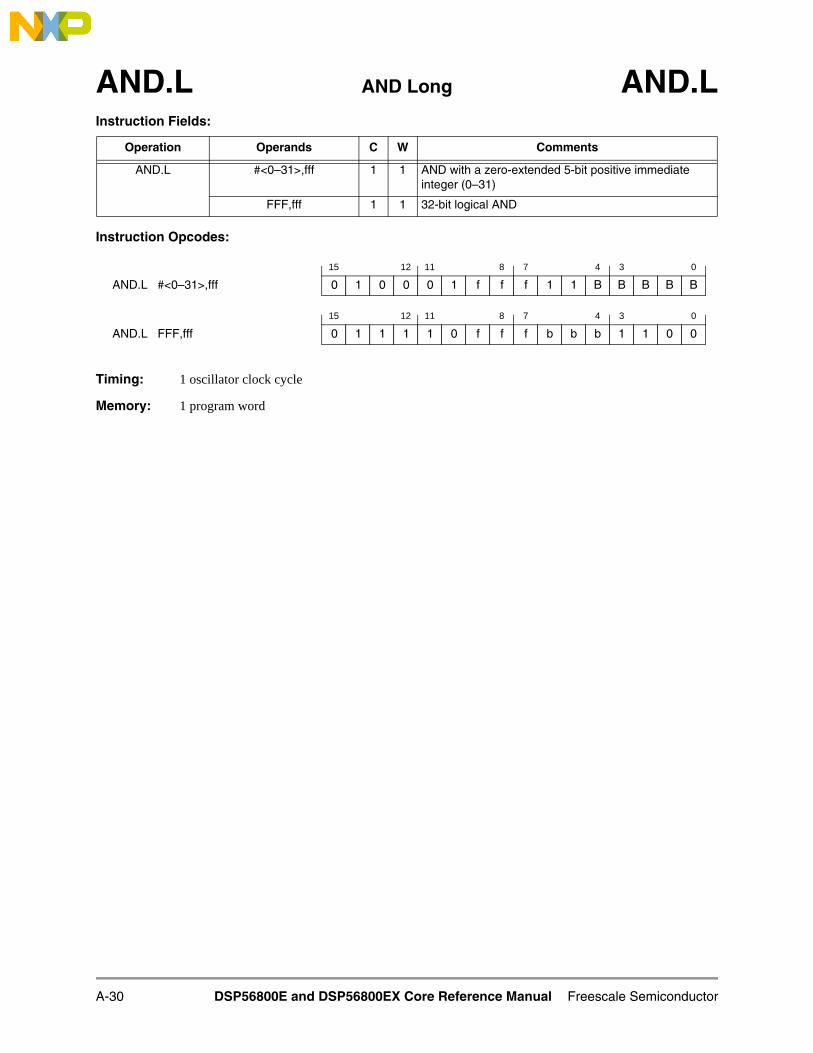
AND.L AND Long AND.LInstruction Fields:
Instruction Opcodes:
Timing: 1 oscillator clock cycle
Memory: 1 program word
Operation Operands C W Comments
AND.L #<0–31>,fff 1 1 AND with a zero-extended 5-bit positive immediate integer (0–31)
FFF,fff 1 1 32-bit logical AND
15 12 11 8 7 4 3 0
AND.L #<0–31>,fff 0 1 0 0 0 1 f f f 1 1 B B B B B
15 12 11 8 7 4 3 0
AND.L FFF,fff 0 1 1 1 1 0 f f f b b b 1 1 0 0
A-30 DSP56800E and DSP56800EX Core Reference Manual Freescale Semiconductor

AND.W AND Word AND.WOperation: Assembler Syntax:
S • D → D (no parallel move) AND.W S,D (no parallel move)S • D[31:16] → D[31:16] (no parallel move) AND.W S,D (no parallel move)
where • denotes the logical AND operator
Description: Perform a logical AND operation on the source operand (S) and the destination operand (D), and storethe result in the destination. This instruction is a 16-bit operation. If the destination is a 36-bit accumu-lator, the operation is performed on the source and bits 31–16 of the accumulator. The remaining bitsof the destination accumulator are not affected. If the source is an immediate 5-bit constant, it is firstzero extended to form a 32-bit operand. The result is not affected by the state of the saturation bit (SA).
Usage: This instruction is used for the logical AND of two registers or of a register and a small immediatevalue. The ANDC instruction is appropriate for performing an AND operation on a 16-bit immediatevalue and a register or memory location.
Example:
AND.W X0,A ; logically AND X0 with A1
Explanation of Example:Prior to execution, the 16-bit X0 register contains the value $7F00, and the 36-bit A accumulator con-tains the value $6:1234:5678. The AND.W X0,A instruction performs a logical AND operation on the16-bit value in the X0 register and on bits 31–16 of the A accumulator (A1), and it stores the 36-bitresult in the A accumulator. Bits 35–32 in the A2 register and bits 15–0 in the A0 register are not af-fected by this instruction.
Condition Codes Affected:
N — Set if bit 31 of accumulator result or MSB of register result is setZ — Set if bits 31–16 of accumulator result or all bits of register result are zeroV — Always cleared
Before Execution
567812346
A2 A1 A0
7F00X0
After Execution
567812006
A2 A1 A0
7F00X0
030FSR 0301SR
LF P4 P3 P2 P1 P0 I1 I0 SZ L E U N Z V C
MR CCR
15 14 13 12 11 10 9 8 7 6 5 4 3 2 1 0
Freescale Semiconductor Instruction Set Details A-31

AND.W AND Word AND.WInstruction Fields:
Instruction Opcodes:
Timing: 1 oscillator clock cycle
Memory: 1 program word
Operation Operands C W Comments
AND.W #<0–31>,EEE 1 1 AND with a zero-extended 5-bit positive immediate inte-ger (0–31)
EEE,EEE 1 1 16-bit logical AND
15 12 11 8 7 4 3 0
AND.W #<0–31>,EEE 0 1 0 1 0 1 E E E 1 1 B B B B B
15 12 11 8 7 4 3 0
AND.W EEE,EEE 0 1 1 1 1 0 E E E a a a 1 0 0 0
A-32 DSP56800E and DSP56800EX Core Reference Manual Freescale Semiconductor

ANDC Logical AND Immediate ANDCOperation: Assembler Syntax:
#xxxx • D → D (no parallel move) ANDC #iiii,D (no parallel move)#xxxx • X:<ea> → X:<ea> (no parallel move) ANDC #iiii,X:<ea>(no parallel move)where • denotes the logical AND operator
Implementation Note:This instruction is implemented by the assembler as an alias to the BFCLR instruction, with the 16-bitimmediate value inverted (one’s-complement) and used as the bit mask. It will dis-assemble as a BFCLR instruction.
Description: Perform a logical AND operation on a 16-bit immediate data value with the destination operand, andstore the results back into the destination. C is also modified as described in “Condition Codes Affect-ed.” This instruction performs a read-modify-write operation on the destination and requires two des-tination accesses.
Example:
ANDC #$0055,X:$5000 ; AND with immediate data
Explanation of Example:Prior to execution, the 16-bit X memory location X:$5000 contains the value $FFFF. Execution of theinstruction performs a logical AND operation on the 16-bit value in X:$5000 (that is, $FFFF) and themask value $0055 and stores the result in X:$5000. The C bit is set because all of the bits selected bythe inverted value of the mask are set.
Condition Codes Affected:
For destination operand SR:For this destination only, the C bit is not updated as is done for all other destination operands.All SR bits except bits 14–10 are updated with values from the bitfield unit. Bits 14–10 of the mask operand must be set.
For other destination operands:L — Set if data limiting occurred during 36-bit source moveC — Set if all bits specified by the one’s-complement of the mask are set
Cleared if at least 1 bit specified by the one’s-complement of the mask is not set
Note: If all bits in the mask are set, the instruction executes two NOPs and sets the C bit.
Instruction Fields:Refer to the section on the BFCLR instruction for legal operand and timing information.
Before Execution
FFFFX:$5000
0300SR
After Execution
0055X:$5000
0301SR
LF P4 P3 P2 P1 P0 I1 I0 SZ L E U N Z V C
MR CCR
15 14 13 12 11 10 9 8 7 6 5 4 3 2 1 0
Freescale Semiconductor Instruction Set Details A-33

ASL Arithmetic Shift Left ASLOperation: Assembler Syntax:
(see following figure) ASL D (no parallel move)ASL D (one parallel move)ASL D (two parallel reads)
:
Description: Arithmetically shift the destination operand (D) 1 bit to the left, and store the result in the destination.The MSB of the destination prior to the execution of the instruction is shifted into C, and a zero is shift-ed into the LSB of the destination. If the destination is the Y register, the MSB is bit 31. A duplicatedestination is not allowed when ASL is used in conjunction with a parallel read. For arithmetic shiftsleft on 16-bit registers, refer to ASL.W.
Usage: This instruction can be used to cast a long to an integer value.
Example:
ASL A X:(R3)+N,Y0; shift A left by 1, update R3 and Y0
Explanation of Example:Prior to execution, the 36-bit A accumulator contains the value $A:0111:0222. Execution of the ASLinstruction shifts the 36-bit value in the A accumulator 1 bit to the left and stores the result back in theA accumulator. C is set by the operation because bit 35 of A was set prior to the execution of the in-struction. The V bit of CCR (bit 1) is also set because bit 35 of A has changed during the execution ofthe instruction. The U bit of CCR (bit 4) is set because the result is not normalized, the E bit of CCR(bit 5) is set because the extension portion of the result is in use, and the L bit of CCR (bit 6) is setbecause an overflow has occurred. A new value for register Y0 is read and address register R3 is up-dated by the contents on index register N.
Condition Codes Affected:
SZ — Set according to the standard definition of SZ (parallel move)L — Set if limiting (parallel move) or overflow has occurred in resultE — Set if the extension portion of accumulator result is in useU — Set according to the standard definition of the U bitN — Set if bit 35 of accumulator result is setZ — Set if accumulator result equals zeroV — Set if bit 35 of accumulator result is changed due to left shiftC — Set if bit 35 of accumulator was set prior to the execution of the instruction
C
D0D2 D1
0
Before Execution
02220111A
A2 A1 A0
0300SR
After Execution
044402224
A2 A1 A0
0373SR
LF P4 P3 P2 P1 P0 I1 I0 SZ L E U N Z V C
MR CCR
15 14 13 12 11 10 9 8 7 6 5 4 3 2 1 0
A-34 DSP56800E and DSP56800EX Core Reference Manual Freescale Semiconductor

ASL Arithmetic Shift Left ASLInstruction Fields:
Parallel Moves:
Operation Operands C W Comments
ASL fff 1 1 Arithmetic shift left entire register by 1 bit.
Data ALU Operation Parallel Memory Move
Operation Operands Source Destination1
1.The case where the destination of the data ALU operation is the same register as the destination of the par-allel read operation is not allowed. Memory writes are allowed in this case.
ASL2
2.This instruction occupies only 1 program word and executes in 1 cycle for every addressing mode.
F X:(Rj)+X:(Rj)+N
X0Y1Y0ABCA1B1
X0Y1Y0ABCA1B1
X:(Rj)+X:(Rj)+N
Freescale Semiconductor Instruction Set Details A-35

ASL Arithmetic Shift Left ASLParallel Dual Reads:
Instruction Opcodes:
Timing: 1 oscillator clock cycle
Memory: 1 program word
Data ALU Operation1
1.This instruction is not allowed when the XP bit in the OMR is set (that is, when the instructions are executingfrom data memory).
First Memory Read Second Memory Read
Operation Operands Source 1 Destination 1 Source 2 Destination 2
ASL2
2.This instruction occupies only 1 program word and executes in 1 cycle for every addressing mode.
F X:(R0)+X:(R0)+NX:(R1)+
X:(R1)+N
Y0Y1
X:(R3)+X:(R3)–
X0
X:(R4)+X:(R4)+N
Y0 X:(R3)+X:(R3)+N3
X0
X:(R0)+X:(R0)+NX:(R4)+
X:(R4)+N
Y1 X:(R3)+X:(R3)+N3
C
15 12 11 8 7 4 3 0
ASL F GGG,X:<ea_m> 0 0 0 1 0 G G G F 0 1 1 0 m R R
15 12 11 8 7 4 3 0
ASL F X:<ea_m>,GGG 0 0 1 1 0 G G G F 0 1 1 0 m R R
15 12 11 8 7 4 3 0
ASL F X:<ea_m>,reg1 X:<ea_v>,reg2
0 1 1 1 0 1 v v F v 1 1 0 m 0 v
15 12 11 8 7 4 3 0
ASL fff 0 1 1 1 0 0 f f f 1 1 0 0 0 1 1
A-36 DSP56800E and DSP56800EX Core Reference Manual Freescale Semiconductor

ASL.W Arithmetic Shift Left ASL.WOperation: Assembler Syntax:
(see following figure) ASL.W D (no parallel move):
Description: Arithmetically shift the destination operand (D) 1 bit to the left, and store the result in the destinationregister. The MSB, bit 15 of the destination prior to the execution of the instruction, is shifted into C,and a zero is shifted into the LSB of the destination. This instruction is used only when the destinationis X0, Y0, or Y1 register. For the purpose of calculating condition code, the 16-bit register is first signextended and concatenated to 16 zero bits to form a 36-bit operand. For arithmetic shifts left on the Yregister or accumulator, refer to ASL.
Example:
ASL.W Y0 ; shift Y0 left by 1
Explanation of Example:Prior to execution, the 16-bit Y0 register contains the value $C000. Execution of the ASL.W instruc-tion shifts the 16-bit value in Y0 by 1 bit to the left and stores the result back in Y0. C is set by theoperation because bit 15 of Y0 was set prior to the execution of the instruction. The N bit is set becausethe MSB of the result is set.
Condition Codes Affected:
L — Set if overflow has occurred in resultE — Set if the extension portion of the result is in useU — Set according to the standard definition of the U bitN — Set if bit 15 of result is setZ — Set if the result equals zeroV — Set if bit 15 of result is changed due to left shiftC — Set if bit 15 of was set prior to the execution of the instruction
C 0
015
Before Execution
0300SR
After Execution
0309SR
C0002000
Y1 Y0
80002000
Y1 Y0
LF P4 P3 P2 P1 P0 I1 I0 SZ L E U N Z V C
MR CCR
15 14 13 12 11 10 9 8 7 6 5 4 3 2 1 0
Freescale Semiconductor Instruction Set Details A-37

ASL.W Arithmetic Shift Left ASL.WInstruction Fields:
Instruction Opcodes:
Timing: 1 oscillator clock cycle
Memory: 1 program word
Operation Operands C W Comments
ASL.W DD 1 1 Arithmetic shift left entire register by 1 bit
15 12 11 8 7 4 3 0
ASL.W DD 0 1 1 1 0 0 1 D D 1 1 0 0 0 1 1
A-38 DSP56800E and DSP56800EX Core Reference Manual Freescale Semiconductor

ASL16 Arithmetic Shift Left 16 Bits ASL16Operation: Assembler Syntax:
S << 16 → D (no parallel move) ASL16 S,D (no parallel move)
Description: Arithmetically shift the source operand to the left by 16 bits, and store the result in the destination (D).This operation effectively places the LSP of the source register into the MSP of the destination register.The low-order 16 bits of the destination are always set to zero. Bits are shifted into the extension reg-ister (FF2) if the destination is an accumulator. When the destination operand is a 16-bit register, theLSP of an accumulator or Y register is written to it. When both the source and destination are 16-bitregisters, the destination is cleared. The result is not affected by the state of the saturation bit (SA).
Example:
ASL16 Y,A ; shift Y left 16 bits, store in A
Explanation of Example:Prior to execution, the Y register contains the value to be shifted ($0000:7FFF). The contents of thedestination register are not important prior to execution because they have no effect on the calculatedvalue. The ASL16 instruction arithmetically shifts the value $0000:7FFF by 16 bits to the left and plac-es the result in the destination register A.
Condition Codes Affected:The condition codes are not affected by this instruction.
Instruction Fields:
Instruction Opcodes:
Timing: 1 oscillator clock cycle
Memory: 1 program word
Operation Operands C W Comments
ASL16 FFF,FFF 1 1 Arithmetic shift left the first operand by 16 bits, placing result in the destination operand
FFF 1 1 An alternate syntax for the preceding instruction if the source and the destination are the same
Before Execution
345634560
A2 A1 A0
After Execution
00007FFF0
A2 A1 A0
7FFF0000
Y1 Y0
7FFF0000
Y1 Y0
15 12 11 8 7 4 3 0
ASL16 FFF,FFF 0 1 1 1 1 1 F F F b b b 0 1 0 1
Freescale Semiconductor Instruction Set Details A-39

ASLA 1-Bit Left Shift AGU Register ASLAOperation: Assembler Syntax:
S << 1 → D (no parallel move) ASLA S,D (no parallel move)
Description: Arithmetically shift the source address register 1 bit to the left, and store the result in the destinationregister.
Example:
ASLA R1,R0 ; shift R1 left 1 bit and store in R0
Explanation of Example:Prior to execution, the R1 register contains the value $004444, and the R0 register contains $00B360.Execution of the ASLA instruction shifts the value in R1 by 1 bit to the left and stores the result($008888) in the R0 register.
Condition Codes Affected:The condition codes are not affected by this instruction.
Instruction Fields:
Instruction Opcodes:
Timing: 1 oscillator clock cycle
Memory: 1 program word
Operation Operands C W Comments
ASLA Rn,Rn 1 1 Arithmetic shift left AGU register by 1 bit
Rn 1 1 An alternate syntax for the preceding instruction if the source and the destination are the same
Before Execution
004444R1
After Execution
00B360R0 008888R0
004444R1
15 12 11 8 7 4 3 0
ASLA Rn,Rn 1 0 0 0 0 0 0 0 n 0 1 n R n R R
A-40 DSP56800E and DSP56800EX Core Reference Manual Freescale Semiconductor

ASLL.L Multi-Bit Arithmetic Left Shift Long ASLL.LOperation: Assembler Syntax:
If S[15] = 0 or S is not a register,D << S → D (no parallel move) ASLL.L S,D (no parallel move)ElseD >> –S → D (no parallel move) ASLL.L S,D (no parallel move)
Description: Arithmetically shift the second operand to the left by the value contained in the 5 lowest bits of the firstoperand (or by an immediate integer). Store the result back in the destination (D) with zeros shiftedinto the LSB. The shift count can be a 5-bit positive immediate integer or the value contained in X0,Y0, Y1, or the MSP of an accumulator. For 36- and 32-bit destinations, the MSP:LSP are shifted withsign extension from bit 31 (the FF2 portion is ignored). If the shift count in a register is negative (bit15 is set), the direction of the shift is reversed, maintaining sign integrity. The result is not affected bythe state of the saturation bit (SA).
Example:
ASLL.L Y0,A ; shift A left by amount in Y0 and store in A
Explanation of Example:Prior to execution, the A accumulator contains the value to be shifted ($0123:4567), and the Y0 regis-ter contains the amount by which to shift ($04). The ASLL.L instruction arithmetically shifts the value$0123:4567 by 4 bits to the left and places the result in the destination register A. Since the destinationis an accumulator, the extension word (A2) is filled with sign extension.
Condition Codes Affected:
N — Set if MSB of result is setZ — Set if result equals zero
Before Execution
456701230
A2 A1 A0
After Execution
567012340
A2 A1 A0
0300SR 0300SR
00242000
Y1 Y0
00242000
Y1 Y0
LF P4 P3 P2 P1 P0 I1 I0 SZ L E U N Z V C
MR CCR
15 14 13 12 11 10 9 8 7 6 5 4 3 2 1 0
Freescale Semiconductor Instruction Set Details A-41

ASLL.L Multi-Bit Arithmetic Left Shift Long ASLL.LInstruction Fields:
Instruction Opcodes:
Timing: 2 oscillator clock cycles
Memory: 1 program word
Operation Operands C W Comments
ASLL.L #<0–31>,fff 2 1 Arithmetic shift left by a 5-bit positive immediate integer
EEE,FFF 2 1 Bi-directional arithmetic shift of destination by value in the first operand: positive –> left shift
15 12 11 8 7 4 3 0
ASLL.L #<0–31>,fff 0 1 0 0 0 1 f f f 0 1 B B B B B
15 12 11 8 7 4 3 0
ASLL.L EEE,FFF 0 1 1 1 1 1 F F F a a a 1 1 1 0
A-42 DSP56800E and DSP56800EX Core Reference Manual Freescale Semiconductor

ASLL.W Multi-Bit Arithmetic Left Shift Word ASLL.WOperation: Assembler Syntax:
S1 << S2 → D (no parallel move) ASLL.W S1,S2,D (no parallel move)D << S → D (no parallel move) ASLL.W S,D (no parallel move)
Description: This instruction can have two or three operands. It arithmetically shifts the source operand S1 or D tothe left by the value contained in the lowest 4 bits of either S2 or S, respectively (or by an immediateinteger), and stores the result in the destination (D) with zeros shifted into the LSB. The shift count canbe a 4-bit positive integer, a value in a 16-bit register, or the MSP of an accumulator. For 36- and 32-bitdestinations, only the MSP is shifted and the LSP is cleared, with sign extension from bit 31 (the FF2portion is ignored). The result is not affected by the state of the saturation bit (SA).
Example:
ASLL.W Y1,X0,A ; shift Y1 left by amount in X0 and store in A
Explanation of Example:Prior to execution, the Y1 register contains the value to be shifted ($AAAA), and the least significant4 bits of the X0 register contain the amount by which to shift ($4). The contents of the destination reg-ister are not important prior to execution because they have no effect on the calculated value. TheASLL.W instruction arithmetically shifts the value $AAAA by 4 bits to the left and places the resultin the destination register A. Since the destination is an accumulator, the extension word (A2) is filledwith sign extension, and the LSP (A0) is cleared.
Condition Codes Affected:
N — Set if MSB of result is setZ — Set if result equals zero
Note: If the CM bit is set, N is cleared. When the destination is a 16-bit register, condition codes are basedon the 16-bit result.
Before Execution
345634560
A2 A1 A0
0014X0
After Execution
0000AAA0F
A2 A1 A0
0014X0
0300SR
0308SR
8000AAAA
Y1 Y0
8000AAAA
Y1 Y0
LF P4 P3 P2 P1 P0 I1 I0 SZ L E U N Z V C
MR CCR
15 14 13 12 11 10 9 8 7 6 5 4 3 2 1 0
Freescale Semiconductor Instruction Set Details A-43

ASLL.W Multi-Bit Arithmetic Left Shift Word ASLL.WInstruction Fields:
Instruction Opcodes:
Timing: 1 oscillator clock cycle
Memory: 1 program word
Operation Operands C W Comments
ASLL.W #<0–15>,FFF 1 1 Arithmetic shift left by a 4-bit positive immediate integer
EEE,FFF 1 1 Arithmetic shift left destination by value specified in 4 LSBs of the first operand
Y1,X0,FFFY0,X0,FFFY1,Y0,FFFY0,Y0,FFFA1,Y0,FFFB1,Y1,FFFC1,Y0,FFFC1,Y1,FFF
1 1 Arithmetic shift left the first operand by value specified in 4 LSBs of the second operand; place result in FFF
15 12 11 8 7 4 3 0
ASLL.W #<0–15>,FFF 0 1 0 1 1 1 F F F 1 1 1 B B B B
15 12 11 8 7 4 3 0
ASLL.W EEE,FFF 0 1 1 1 1 1 F F F a a a 1 0 1 0
15 12 11 8 7 4 3 0
ASLL.W Q1,Q2,FFF 0 1 1 1 0 0 F F F Q Q Q 1 1 1 0
A-44 DSP56800E and DSP56800EX Core Reference Manual Freescale Semiconductor

ASR Arithmetic Shift Right ASROperation: Assembler Syntax:
(see following figure) ASR D (no parallel move)ASR D (one parallel move)ASR D (two parallel reads)
Description: Arithmetically shift the destination operand (D) 1 bit to the right and store the result in the destinationaccumulator. The LSB of the destination prior to the execution of the instruction is shifted into C, andthe MSB of the destination is held constant. When the destination register is Y or a 16-bit register, theMSB is bit 31 or bit 15, respectively. A duplicate destination is not allowed when ASR is used in con-junction with a parallel read.
Example:
ASR B X:(R3)+,Y0; divide B by 2, load Y0, and update R3
Explanation of Example:Prior to execution, the 36-bit B accumulator contains the value $8:AAAA:AAAA. Execution of theASR instruction shifts the 36-bit value in the B accumulator 1 bit to the right and stores the result backin the B accumulator. C is cleared by the operation because bit 0 of A was cleared prior to the executionof the instruction. The N bit of CCR (bit 3) is set because bit 35 of the result in A is set. The E bit ofCCR (bit 5) is set because the extension portion of B is used by the result.
Condition Codes Affected:
SZ — Set according to the standard definition of the SZ bit (parallel move)L — Set if data limiting has occurred during parallel moveE — Set if the extension portion of result is in useU — Set according to the standard definition of the U bitN — Set if MSB of result is setZ — Set if result equals zeroV — Always clearedC — Set if bit 0 of source operand was set prior to the execution of the instruction
Note: Condition code results depend on the size of the destination operand.
(parallel move)
D0D2 D1
C
MSB
Before Execution
AAAAAAAA8
B2 B1 B0
0300SR
After Execution
55555555C
B2 B1 B0
0328SR
LF P4 P3 P2 P1 P0 I1 I0 SZ L E U N Z V C
MR CCR
15 14 13 12 11 10 9 8 7 6 5 4 3 2 1 0
Freescale Semiconductor Instruction Set Details A-45

ASR Arithmetic Shift Right ASRInstruction Fields:
Parallel Moves:
Operation Operands C W Comments
ASR FFF 1 1 Arithmetic shift right entire register by 1 bit.
Data ALU Operation Parallel Memory Move
Operation Operands Source Destination1
1.The case where the destination of the data ALU operation is the same register as the destination of the par-allel read operation is not allowed. Memory writes are allowed in this case.
ASR2
2.This instruction occupies only 1 program word and executes in 1 cycle for every addressing mode.
F X:(Rj)+X:(Rj)+N
X0Y1Y0ABCA1B1
X0Y1Y0ABCA1B1
X:(Rj)+X:(Rj)+N
A-46 DSP56800E and DSP56800EX Core Reference Manual Freescale Semiconductor

ASR Arithmetic Shift Right ASRParallel Dual Reads:
Instruction Opcodes:
Timing: 1 oscillator clock cycle
Memory: 1 program word
Data ALU Operation1
1.This instruction is not allowed when the XP bit in the OMR is set (that is, when the instructions are executingfrom data memory).
First Memory Read Second Memory Read
Operation Operands Source 1 Destination 1 Source 2 Destination 2
ASR2
2.This instruction occupies only 1 program word and executes in 1 cycle for every addressing mode.
F X:(R0)+X:(R0)+NX:(R1)+
X:(R1)+N
Y0Y1
X:(R3)+X:(R3)–
X0
X:(R4)+X:(R4)+N
Y0 X:(R3)+X:(R3)+N3
X0
X:(R0)+X:(R0)+NX:(R4)+
X:(R4)+N
Y1 X:(R3)+X:(R3)+N3
C
15 12 11 8 7 4 3 0
ASR F GGG,X:<ea_m> 0 0 0 1 1 G G G F 0 1 1 0 m R R
15 12 11 8 7 4 3 0
ASR F X:<ea_m>,GGG 0 0 1 1 1 G G G F 0 1 1 0 m R R
15 12 11 8 7 4 3 0
ASR F X:<ea_m>,reg1X:<ea_v>,reg2
0 1 1 1 0 1 v v F v 1 0 0 m 0 v
15 12 11 8 7 4 3 0
ASR FFF 0 1 1 1 0 0 F F F 1 1 0 1 0 1 1
Freescale Semiconductor Instruction Set Details A-47

ASR16 Arithmetic Shift Right 16 Bits ASR16Operation: Assembler Syntax:
S >> 16 → D (no parallel move) ASR16 S,D (no parallel move)
Description: Arithmetically shift the source operand to the right by 16 bits, and store the result in the destination(D), sign extending to the left. This operation effectively places the MSP of the source register into theLSP of the destination register, propagating the sign bit through the MSP (and the extension registerfor accumulator destinations). If the source is an accumulator, both the extension register and MSP areshifted. When the destination operand is a 16-bit register, the sign information is written to it. For ex-ample, if the source is an accumulator, the 4 bits of the EXT are written to the lower 4 bits of the des-tination register with sign extension. If the source is a 16-bit register or the Y register, the msb (signbit) is written with sign extension. The result is not affected by the state of the saturation bit (SA).
Usage: This instruction can be used to cast an integer to a long value.
Example 1:ASR16 Y,A ; shift long in Y right by 16 bits and place in A
Explanation of Example:Prior to execution, the Y register contains the value to be shifted ($A1A2:A3A4). The contents of thedestination register are not important prior to execution because they have no effect on the calculatedvalue. The ASR16 instruction arithmetically shifts the value $A1A2:A3A4 by 16 bits to the right, signextends to a full 36 bits, and places the result in the destination register A.
Example 2:ASR16 Y,X0 ; shift sign bit in Y right by 16 bits and sign extend
Explanation of Example:Prior to execution, the Y register contains the value to be shifted ($A3A2:A1A0). The contents of thedestination register are not important prior to execution because they have no effect on the calculatedvalue. Since the destination is a 16-bit register, the ASR16 instruction arithmetically shifts the valueof the sign bit by 16 bits to the right with sign extension, and places the result in the destination registerX0.
Condition Codes Affected:The condition codes are not affected by this instruction.
Before Execution
345634560
A2 A1 A0
After Execution
A1A2FFFFF
A2 A1 A0
A3A4A1A2
Y1 Y0
A3A4A1A2
Y1 Y0
Before Execution
A1A0A3A2
Y1 Y0
After Execution
A1A0A3A2
Y1 Y0
0000
X0
FFFF
X0
A-48 DSP56800E and DSP56800EX Core Reference Manual Freescale Semiconductor

ASR16 Arithmetic Shift Right 16 Bits ASR16Instruction Fields:
Instruction Opcodes:
Timing: 1 oscillator clock cycle
1 program word
Memory: 1 program word
Operation Operands C W Comments
ASR16 FFF,FFF 1 1 Arithmetic shift right the first operand by 16 bits, placing result in the destination operand.
FFF 1 1 An alternate syntax for the above instruction if the source and the destination are the same.
15 12 11 8 7 4 3 0
ASR16 FFF,FFF 0 1 1 1 1 1 F F F b b b 0 1 1 0
Freescale Semiconductor Instruction Set Details A-49

ASRA 1-Bit Arithmetic Shift Right AGU Register ASRAOperation: Assembler Syntax:
D >> 1 → D (no parallel move) ASRA D (no parallel move)
Description: Arithmetically shift the address register operand 1 bit to the right, and store the result back in the reg-ister.
Example:
ASRA R0 ; arithmetically shift R0 to the right 1 bit
Explanation of Example:Prior to execution, the R0 register contains $80B360. Execution of the ASRA instruction shifts the val-ue in the R0 register 1 bit to the right and stores the result ($C059B0) back in R0.
Condition Codes Affected:The condition codes are not affected by this instruction.
Instruction Fields:
Instruction Opcodes:
Timing: 1 oscillator clock cycle
Memory: 1 program word
Operation Operands C W Comments
ASRA Rn 1 1 Arithmetic shift right AGU register by 1 bit
Before Execution After Execution
80B360R0 C059B0R0
15 12 11 8 7 4 3 0
ASRA Rn 1 0 0 0 0 1 0 1 0 0 1 1 R 0 R R
A-50 DSP56800E and DSP56800EX Core Reference Manual Freescale Semiconductor

ASRAC Arithmetic Right Shift with Accumulate ASRACOperation: Assembler Syntax:
(S1 >> S2) + D → D (no parallel move) ASRAC S1,S2,D (no parallel move)
Description: Arithmetically shift the first 16-bit source operand (S1) to the right by the value contained in the lowest4 bits of the second source operand (S2), and accumulate the result with the value in the destination(D). Operand S1 is internally sign extended and concatenated with 16 zero bits to form a 36-bit valuebefore the shift operation. The result is not affected by the state of the saturation bit (SA).
Usage: This instruction is typically used for multi-precision arithmetic right shifts.
Example:
ASRAC Y1,X0,A ; arithmetic right shift Y1 by 4 and; accumulate in A
Explanation of Example:Prior to execution, the Y1 register contains the value that is to be shifted ($C003), the X0 register con-tains the amount by which to shift ($4), and the destination accumulator contains $0:0000:0099. TheASRAC instruction arithmetically shifts the value $C003 by 4 bits to the right and accumulates thisresult with the value that is already in the destination register A.
Condition Codes Affected:
N — Set if bit 35 of accumulator result is setZ — Set if accumulator result equals zero
Note: If the SA bit is set, the N bit is equal to bit 31 of the result.If the SA bit is clear, the N bit is equal to bit 35 of the result.
Before Execution
009900000
A2 A1 A0
00F4X0
After Execution
3099FC00F
A2 A1 A0
00F4X0
0300SR 0308SR
8000C003
Y1 Y0
8000C003
Y1 Y0
LF P4 P3 P2 P1 P0 I1 I0 SZ L E U N Z V C
MR CCR
15 14 13 12 11 10 9 8 7 6 5 4 3 2 1 0
Freescale Semiconductor Instruction Set Details A-51

ASRAC Arithmetic Right Shift with Accumulate ASRACInstruction Fields:
Instruction Opcodes:
Timing: 1 oscillator clock cycle
Memory: 1 program word
Operation Operands C W Comments
ASRAC Y1,X0,FFY0,X0,FFY1,Y0,FFY0,Y0,FFA1,Y0,FFB1,Y1,FFC1,Y0,FFC1,Y1,FF
1 1 Arithmetic word shift with accumulation
15 12 11 8 7 4 3 0
ASRAC Q1,Q2,FF 0 1 1 1 0 0 0 F F Q Q Q 0 1 1 0
A-52 DSP56800E and DSP56800EX Core Reference Manual Freescale Semiconductor

ASRR.L Multi-Bit Arithmetic Right Shift Long ASRR.LOperation: Assembler Syntax:
If S[15] = 0 or S is not a register,D >> S → D (no parallel move) ASRR.L S,D (no parallel move)ElseD << –S → D (no parallel move) ASRR.L S,D (no parallel move)
Description: Arithmetically shift the second operand to the right by the value contained in the 5 lowest bits of thefirst operand (or by an immediate integer), and store the result back in the destination (D). The shiftcount can be a 5-bit positive immediate integer or the value contained in X0, Y0, Y1, or the MSP ofan accumulator. For 36- and 32-bit destinations, the MSP:LSP are shifted, with sign extension from bit31 (the FF2 portion is ignored). If the shift count in a register is negative (bit 15 is set), the directionof the shift is reversed, maintaining sign integrity. The result is not affected by the state of the satura-tion bit (SA).
Example:
ASRR.L Y0,A ; shift A right by the amount in Y0 and; store result in A
Explanation of Example:Prior to execution, the A accumulator contains the value that is to be shifted ($0123:4567), and the Y0register contains the amount by which to shift ($FFFC). Since the count is a negative number, the shiftis reversed—that is, the value will be shifted left. The ASRR.L instruction arithmetically shifts the val-ue $0123:4567 by 4 bits to the left and places the result in the destination register A.
Condition Codes Affected:
N — Set if the MSB of the result is setZ — Set if the result equals zero
Note: Condition code results depend on the size of the destination operand.
Before Execution
456701230
A2 A1 A0
After Execution
567012340
A2 A1 A0
0300SR 0300SR
FFFC2000
Y1 Y0
FFFC2000
Y1 Y0
LF P4 P3 P2 P1 P0 I1 I0 SZ L E U N Z V C
MR CCR
15 14 13 12 11 10 9 8 7 6 5 4 3 2 1 0
Freescale Semiconductor Instruction Set Details A-53

ASRR.L Multi-Bit Arithmetic Right Shift Long ASRR.LInstruction Fields:
Instruction Opcodes:
Timing: 2 oscillator clock cycles
Memory: 1 program word
Operation Operands C W Comments
ASRR.L #<0–31>,fff 2 1 Arithmetic shift right by a 5-bit positive immediate integer
EEE,FFF 2 1 Bi-directional arithmetic shift of destination by value in the first operand: positive –> right shift
15 12 11 8 7 4 3 0
ASRR.L #<0–31>,fff 0 1 0 0 1 1 f f f 1 1 B B B B B
15 12 11 8 7 4 3 0
ASRR.L EEE,FFF 0 1 1 1 1 1 F F F a a a 1 1 0 0
A-54 DSP56800E and DSP56800EX Core Reference Manual Freescale Semiconductor

ASRR.W Multi-Bit Arithmetic Right Shift Word ASRR.WOperation: Assembler Syntax:
S1 >> S2 → D (no parallel move) ASRR.W S1,S2,D (no parallel move)D >> S → D (no parallel move) ASRR.W S,D (no parallel move)
Description: This instruction can have two or three operands. Arithmetically shift either the source operand S1 orD to the right by the value contained in the lowest 4 bits of either S2 or S, respectively (or by an im-mediate integer), and store the result in the destination (D). The shift count can be a 4-bit positive in-teger, a value in a 16-bit register, or the MSP of an accumulator. For 36- and 32-bit destinations, onlythe MSP is shifted and the LSP is cleared, with sign extension from bit 31 (the FF2 portion is ignored).The result is not affected by the state of the saturation bit (SA).
Example 1: ASRR.W Y1,Y0,A ; arithmetic right shift of 16-bit Y1 by; least 4 bits of Y0
Explanation of Example:Prior to execution, the Y1 register contains the value that is to be shifted ($AAAA), and the Y0 registercontains the number by which to shift (least 4 bits of $FFF1 = 1). The contents of the destination reg-ister are not important prior to execution because they have no effect on the calculated value. The ASRR.W instruction arithmetically shifts the value $AAAA by 1 bit to the right and places the resultin the destination register A with sign extension (the LSP is cleared).
Example 2: ASRR.W Y1,A ; arithmetic right shift of 16-bit A1 by; least 4 bits of Y1
Explanation of Example:Prior to execution, A1 contains the value that is to be shifted ($AAAA), and the Y1 register containsthe amount by which to shift ($1). The ASRR.W instruction arithmetically shifts the sign extended val-ue $AAAA by 1 bit to the right and places the result in the destination register A (the LSP is cleared).
Before Execution
567812340
A2 A1 A0
After Execution
0000D555F
A2 A1 A0
0300SR 0308SR
FFF1AAAA
Y1 Y0
FFF1AAAA
Y1 Y0
Before Execution
4567AAAA0
A2 A1 A0
After Execution
0000D555F
A2 A1 A0
0300SR 0308SR
000F0001
Y1 Y0
000F0001
Y1 Y0
Freescale Semiconductor Instruction Set Details A-55

ASRR.W Multi-Bit Arithmetic Right Shift Word ASRR.WCondition Codes Affected:
N — Set if MSB of result is setZ — Set if result equals zero
Instruction Fields:
Instruction Opcodes:
Timing: 1 oscillator clock cycle
Memory: 1 program word
Operation Operands C W Comments
ASRR.W #<0–15>,FFF 1 1 Arithmetic shift right by a 4-bit positive immediate integer
EEE,FFF 1 1 Arithmetic shift right the destination by value specified in 4 LSBs of the first operand
Y1,X0,FFFY0,X0,FFFY1,Y0,FFFY0,Y0,FFFA1,Y0,FFFB1,Y1,FFFC1,Y0,FFFC1,Y1,FFF
1 1 Arithmetic shift right of the first operand by value speci-fied in 4 LSBs of the second operand; place result in FFF
LF P4 P3 P2 P1 P0 I1 I0 SZ L E U N Z V C
MR CCR
15 14 13 12 11 10 9 8 7 6 5 4 3 2 1 0
15 12 11 8 7 4 3 0
ASRR.W #<0–15>,FFF 0 1 0 1 1 1 F F F 1 1 0 B B B B
15 12 11 8 7 4 3 0
ASRR.W EEE,FFF 0 1 1 1 1 1 F F F a a a 1 0 0 0
15 12 11 8 7 4 3 0
ASRR.W Q1,Q2,FFF 0 1 1 1 0 0 F F F Q Q Q 0 0 1 0
A-56 DSP56800E and DSP56800EX Core Reference Manual Freescale Semiconductor

Bcc Branch Conditionally BccOperation: Assembler Syntax:
If (cc), then PC + <OFFSET> → PC Bcc <OFFSET7>else PC + 1 → PC Bcc <OFFSET18>
Bcc <OFFSET22>
Description: If the specified condition is true, program execution continues at the location PC + displacement. ThePC contains the address of the next instruction. If the specified condition is false, the PC is increment-ed, and program execution continues sequentially. The offset can be 7, 18, or 22 bits; 7- and 18-bitoffsets are sign extended to 21 bits.
The term “cc” specifies the following:
Example:
BNE <LABEL ; branch to LABEL if Z condition is zeroINC.W AINC.W A
LABELADD B,A
See Table 3-14 on page 3-27 for usage of forcing operator “<LABEL.”
Explanation of Example:In this example, if the Z bit is zero when the BNE instruction is executed, program execution skips thetwo INC.W instructions and continues with the ADD instruction. If the specified condition is not true,no branch is taken, the program counter is incremented by one, and program execution continues withthe first INC.W instruction. The Bcc instruction uses a PC-relative offset of two for this example.
“cc” Mnemonic Condition
CC (HS*) — carry clear (higher or same) C = 0
CS (LO*) — carry set (lower) C = 1
EQ — equal Z = 1
GE — greater than or equal N ⊕ V = 0
GT — greater than Z + (N ⊕ V) = 0
HI* — higher C • Z = 1
LE — less than or equal Z + (N ⊕ V) = 1
LS* — lower or same C + Z = 1
LT — less than N ⊕ V = 1
NE — not equal Z = 0
NN — not normalized Z + (U • E) = 0
NR — normalized Z + (U • E) = 1
* Only available when CM bit set in the OMR
Xdenotes the logical complement of X+denotes the logical OR operator•denotes the logical AND operator⊕denotes the logical exclusive OR operator
Freescale Semiconductor Instruction Set Details A-57

Bcc Branch Conditionally BccRestrictions:
Refer to Section 10.4, “Pipeline Dependencies and Interlocks,” on page 10-26.
Condition Codes Affected:The condition codes are tested but not modified by this instruction.
Instruction Fields:
Instruction Opcodes:
Timing: 3–6 oscillator clock cycles
Memory: 1–3 program word(s)
Operation Operands C1
1.The clock-cycle count depends on whether the branch is taken. The first value applies if the branch is taken,and the second applies if it is not.
W Comments
Bcc <OFFSET7> 5 or 3 1 7-bit signed offset
<OFFSET18> 5 or 4 2 18-bit signed offset
<OFFSET22> 6 or 5 3 22-bit signed offset
15 12 11 8 7 4 3 0
Bcc <OFFSET7> 1 0 1 0 C C C C 0 A a a a a a a
15 12 11 8 7 4 3 0
Bcc <OFFSET18> 1 1 1 0 0 C C C 0 1 1 0 1 C A A
AAAAAAAAAAAAAAAA
15 12 11 8 7 4 3 0
Bcc <OFFSET22> 1 1 1 0 0 A A A 0 A 1 1 A A A A
1 1 1 0 0 C C C 0 1 1 0 1 C 0 0
AAAAAAAAAAAAAAAA
A-58 DSP56800E and DSP56800EX Core Reference Manual Freescale Semiconductor

BFCHG Test Bitfield and Change BFCHGOperation: Assembler Syntax:
(<bitfield> of destination) → (<bitfield> of destination)BFCHG #iiii,X:<ea> (no parallel move)BFCHG #iiii,D (no parallel move)
Description: Test all selected bits of the destination operand. If all selected bits are set, C is set; otherwise, C iscleared. Then complement the selected bits, and store the result in the destination. A 16-bit immediatevalue is used to specify which bits are tested and changed. Those bits that are set in the immediate valueare the same bits that are tested and changed in the destination; those bits that are cleared in the imme-diate value are ignored in the destination. This instruction performs a read-modify-write operation onthe destination memory location or register and requires two destination accesses.
Usage: This instruction is very useful in performing I/O and flag bit manipulation.
Example:
BFCHG #$0310,X:$5000 ; test and change bits 4, 8, and 9; in a data memory location
Explanation of Example:Prior to execution, the 16-bit X memory location X:$5000 contains the value $0010. Execution of theBFCHG instruction tests the state of bits 4, 8, and 9 in X:$5000, does not set C (because all of the se-lected bits were not set), and then complements the bits.
Condition Codes Affected:
For destination operand SR:For this destination only, the C bit is not updated as is done for all other destination operands.All SR bits except bits 14–10 are updated with values from the bitfield unit. Bits 14–10 of the mask operand must be cleared.
For other destination operands:L — Set if data limiting occurred during 36-bit source moveC — Set if all bits specified by the mask are set
Cleared if at least 1 bit specified by the mask is not set
Note: If all bits in the mask are cleared, the instruction executes two NOPs and sets the C bit.
Before Execution
0010X:$5000
0301SR
After Execution
0300X:$5000
0300SR
LF P4 P3 P2 P1 P0 I1 I0 SZ L E U N Z V C
MR CCR
15 14 13 12 11 10 9 8 7 6 5 4 3 2 1 0
Freescale Semiconductor Instruction Set Details A-59

BFCHG Test Bitfield and Change BFCHGInstruction Fields:
Operation Operands C W Comments
BFCHG #<MASK16>,DDDDD 2 2 BFCHG tests all targeted bits defined by the 16-bit immedi-ate mask. If all targeted bits are set, then the C bit is set. Otherwise it is cleared. Then the instruction inverts all selected bits.
All registers in DDDDD are permitted except HWS and Y.
#<MASK16>,dd 2 2
#<MASK16>,X:(Rn) 2 2
#<MASK16>,X:(Rn+xxxx) 3 3
#<MASK16>,X:(SP–xx) 3 2
#<MASK16>,X:aa 2 2
#<MASK16>,X:<<pp 2 2
#<MASK16>,X:xxxx 3 3
#<MASK16>,X:xxxxxx 4 4
A-60 DSP56800E and DSP56800EX Core Reference Manual Freescale Semiconductor

BFCHG Test Bitfield and Change BFCHGInstruction Opcodes:
Timing: 2–4 oscillator clock cycles
Memory: 2–4 program words
15 12 11 8 7 4 3 0
BFCHG #<MASK16>,DDDDD 1 0 0 0 0 1 0 1 0 1 0 d d d d d
iiiiiiiiiiiiiiii
15 12 11 8 7 4 3 0
BFCHG #<MASK16>,X:(Rn) 1 0 0 0 0 1 0 0 0 1 0 0 R 0 R R
iiiiiiiiiiiiiiii
15 12 11 8 7 4 3 0
BFCHG #<MASK16>,X:(Rn+xxxx) 1 0 0 0 0 1 0 0 0 1 0 0 R 1 R R
AAAAAAAAAAAAAAAA
iiiiiiiiiiiiiiii
15 12 11 8 7 4 3 0
BFCHG #<MASK16>,X:(SP–xx) 1 0 1 0 0 1 0 0 1 1 a a a a a a
iiiiiiiiiiiiiiii
15 12 11 8 7 4 3 0
BFCHG #<MASK16>,X:<<pp 1 0 1 0 0 1 0 1 1 1 p p p p p p
iiiiiiiiiiiiiiii
15 12 11 8 7 4 3 0
BFCHG #<MASK16>,X:xxxx 1 0 0 0 0 1 0 0 0 1 0 1 0 1 0 0
AAAAAAAAAAAAAAAA
iiiiiiiiiiiiiiii
15 12 11 8 7 4 3 0
BFCHG #<MASK16>,X:xxxxxx 1 1 1 0 0 A A A 0 A 1 1 A A A A
1 0 0 0 0 1 0 0 0 1 0 1 0 1 0 0
AAAAAAAAAAAAAAAA
iiiiiiiiiiiiiiii
15 12 11 8 7 4 3 0
BFCHG #<MASK16>,dd 1 0 0 0 0 1 0 0 0 1 0 1 0 0 d d
iiiiiiiiiiiiiiii
15 12 11 8 7 4 3 0
BFCHG #<MASK16>,X:aa 1 0 1 0 0 1 0 1 1 0 p p p p p p
iiiiiiiiiiiiiiii
Freescale Semiconductor Instruction Set Details A-61

BFCLR Test Bitfield and Clear BFCLROperation: Assembler Syntax:
0 →(<bitfield> of destination) (no parallel move) BFCLR #iiii,X:<ea> (no parallel move) BFCLR #iiii,D (no parallel move)
Description: Test all selected bits of the destination operand. If all selected bits are set, C is set; otherwise, C iscleared. Then clear the selected bits, and store the result in the destination. A 16-bit immediate valueis used to specify which bits are tested and cleared. Those bits that are set in the immediate value arethe same bits that are tested and cleared in the destination; those bits that are cleared in the immediatevalue are ignored in the destination. This instruction performs a read-modify-write operation on thedestination memory location or register and requires two destination accesses.
Usage: This instruction is very useful in performing I/O and flag bit manipulation.
Example:
BFCLR #$0310,X:$5000 ; test and clear bits 4, 8, and 9 in; an on-chip peripheral register
Explanation of Example:Prior to execution, the 16-bit X memory location X:$5000 contains the value $7FF5. Execution of theBFCLR instruction tests the state of bits 4, 8, and 9 in X:5000, sets the C bit (because all the selectedbits were set), and then clears the selected bits.
Condition Codes Affected:
For destination operand SR:For this destination only, the C bit is not updated as is done for all other destination operands.All SR bits except bits 14–10 are updated with values from the bitfield unit. Bits 14–10 of the mask operand must be cleared.
For other destination operands:L — Set if data limiting occurred during 36-bit source moveC — Set if all bits specified by the mask are set
Cleared if at least 1 bit specified by the mask is not set
Note: If all bits in the mask are cleared, the instruction executes two NOPs and sets the C bit.
Before Execution
7FF5X:$5000
0300SR
After Execution
7CE5X:$5000
0301SR
LF P4 P3 P2 P1 P0 I1 I0 SZ L E U N Z V C
MR CCR
15 14 13 12 11 10 9 8 7 6 5 4 3 2 1 0
A-62 DSP56800E and DSP56800EX Core Reference Manual Freescale Semiconductor

BFCLR Test Bitfield and Clear BFCLRInstruction Fields:
Operation Operands C W Comments
BFCLR #<MASK16>,DDDDD 2 2 BFCLR tests all the targeted bits defined by the 16-bit immediate mask. If all the targeted bits are set, then the C bit is set. Otherwise it is cleared. Then the instruction clears all selected bits.
All registers in DDDDD are permitted except HWS and Y.
#<MASK16>,dd 2 2
#<MASK16>,X:(Rn) 2 2
#<MASK16>,X:(Rn+xxxx) 3 3
#<MASK16>,X:(SP–xx) 3 2
#<MASK16>,X:aa 2 2
#<MASK16>,X:<<pp 2 2
#<MASK16>,X:xxxx 3 3
#<MASK16>,X:xxxxxx 4 4
Freescale Semiconductor Instruction Set Details A-63

BFCLR Test Bitfield and Clear BFCLR
Timing: 2–4 oscillator clock cycles
Memory: 2–4 program words
15 12 11 8 7 4 3 0
BFCLR #<MASK16>,DDDDD 1 0 0 0 0 0 0 1 0 1 0 d d d d d
iiiiiiiiiiiiiiii
15 12 11 8 7 4 3 0
BFCLR #<MASK16>,X:(Rn) 1 0 0 0 0 0 0 0 0 1 0 0 R 0 R R
iiiiiiiiiiiiiiii
15 12 11 8 7 4 3 0
BFCLR #<MASK16>,X:(Rn+xxxx) 1 0 0 0 0 0 0 0 0 1 0 0 R 1 R R
AAAAAAAAAAAAAAAA
iiiiiiiiiiiiiiii
15 12 11 8 7 4 3 0
BFCLR #<MASK16>,X:(SP–xx) 1 0 1 0 0 0 0 0 1 1 a a a a a a
iiiiiiiiiiiiiiii
15 12 11 8 7 4 3 0
BFCLR #<MASK16>,X:<<pp 1 0 1 0 0 0 0 1 1 1 p p p p p p
iiiiiiiiiiiiiiii
15 12 11 8 7 4 3 0
BFCLR #<MASK16>,X:xxxx 1 0 0 0 0 0 0 0 0 1 0 1 0 1 0 0
AAAAAAAAAAAAAAAA
iiiiiiiiiiiiiiii
15 12 11 8 7 4 3 0
BFCLR #<MASK16>,X:xxxxxx 1 1 1 0 0 A A A 0 A 1 1 A A A A
1 0 0 0 0 0 0 0 0 1 0 1 0 1 0 0
AAAAAAAAAAAAAAAA
iiiiiiiiiiiiiiii
15 12 11 8 7 4 3 0
BFCLR #<MASK16>,dd 1 0 0 0 0 0 0 0 0 1 0 1 0 0 d d
iiiiiiiiiiiiiiii
15 12 11 8 7 4 3 0
BFCLR #<MASK16>,X:aa 1 0 1 0 0 0 0 1 1 0 p p p p p p
iiiiiiiiiiiiiiii
A-64 DSP56800E and DSP56800EX Core Reference Manual Freescale Semiconductor

BFSET Test Bitfield and Set BFSETOperation: Assembler Syntax:
1 → (<bitfield> of destination) (no parallel move) BFSET #iiii,X:<ea> (no parallel move)BFSET #iiii,D (no parallel move)
Description: Test all selected bits of the destination operand. If all selected bits are set, C is set; otherwise, C iscleared. Then set the selected bits, and store the result in the destination memory. A 16-bit immediatevalue is used to specify which bits are tested and set. Those bits that are set in the immediate value arethe same bits that are tested and set in the destination; those bits that are cleared in the immediate valueare ignored in the destination. This instruction performs a read-modify-write operation on the destina-tion memory location or register and requires two destination accesses.
Usage: This instruction is very useful in performing I/O and flag bit manipulation.
Example:
BFSET #$CC00,X:$5000 ; set bits in peripheral register
Explanation of Example:Prior to execution, the 16-bit X memory location X:$5000 contains the value $3300. Execution of theinstruction tests the state of bits 10, 11, 14, and 15 in X:$5000, clears the C bit (because none of theselected bits was set), and then sets the selected bits.
Condition Codes Affected:
For destination operand SR:For this destination only, the C bit is not updated as is done for all other destination operands.All SR bits except bits 14–10 are updated with values from the bitfield unit. Bits 14–10 of the mask operand must be cleared.
For other destination operands:L — Set if data limiting occurred during 36-bit source moveC — Set if all bits specified by the mask are set
Cleared if at least 1 bit specified by the mask is not set
Note: If all bits in the mask are cleared, the instruction executes two NOPs and sets the C bit.
Before Execution
3300X:$5000
0301SR
After Execution
FF00X:$5000
0300SR
LF P4 P3 P2 P1 P0 I1 I0 SZ L E U N Z V C
MR CCR
15 14 13 12 11 10 9 8 7 6 5 4 3 2 1 0
Freescale Semiconductor Instruction Set Details A-65

BFSET Test Bitfield and Set BFSETInstruction Fields:
Operation Operands C W Comments
BFSET #<MASK16>,DDDDD 2 2 BFSET tests all the targeted bits defined by the 16-bit immediate mask. If all the targeted bits are set, then the C bit is set. Otherwise it is cleared. Then the instruction sets all selected bits.
All registers in DDDDD are permitted except HWS and Y.
#<MASK16>,dd 2 2
#<MASK16>,X:(Rn) 2 2
#<MASK16>,X:(Rn+xxxx) 3 3
#<MASK16>,X:(SP–xx) 3 2
#<MASK16>,X:aa 2 2
#<MASK16>,X:<<pp 2 2
#<MASK16>,X:xxxx 3 3
#<MASK16>,X:xxxxxx 4 4
A-66 DSP56800E and DSP56800EX Core Reference Manual Freescale Semiconductor

BFSET Test Bitfield and Set BFSETInstruction Opcodes:
Timing: 2–4 oscillator clock cycles
Memory: 2–4 program words
15 12 11 8 7 4 3 0
BFSET #<MASK16>,DDDDD 1 0 0 0 0 0 1 1 0 1 0 d d d d d
iiiiiiiiiiiiiiii
15 12 11 8 7 4 3 0
BFSET #<MASK16>,X:(Rn) 1 0 0 0 0 0 1 0 0 1 0 0 R 0 R R
iiiiiiiiiiiiiiii
15 12 11 8 7 4 3 0
BFSET #<MASK16>,X:(Rn+xxxx) 1 0 0 0 0 0 1 0 0 1 0 0 R 1 R R
AAAAAAAAAAAAAAAA
iiiiiiiiiiiiiiii
15 12 11 8 7 4 3 0
BFSET #<MASK16>,X:(SP–xx) 1 0 1 0 0 0 1 0 1 1 a a a a a a
iiiiiiiiiiiiiiii
15 12 11 8 7 4 3 0
BFSET #<MASK16>,X:<<pp 1 0 1 0 0 0 1 1 1 1 p p p p p p
iiiiiiiiiiiiiiii
15 12 11 8 7 4 3 0
BFSET #<MASK16>,X:xxxx 1 0 0 0 0 0 1 0 0 1 0 1 0 1 0 0
AAAAAAAAAAAAAAAA
iiiiiiiiiiiiiiii
15 12 11 8 7 4 3 0
BFSET #<MASK16>,X:xxxxxx 1 1 1 0 0 A A A 0 A 1 1 A A A A
1 0 0 0 0 0 1 0 0 1 0 1 0 1 0 0
AAAAAAAAAAAAAAAA
iiiiiiiiiiiiiiii
15 12 11 8 7 4 3 0
BFSET #<MASK16>,dd 1 0 0 0 0 0 1 0 0 1 0 1 0 0 d d
iiiiiiiiiiiiiiii
15 12 11 8 7 4 3 0
BFSET #<MASK16>,X:aa 1 0 1 0 0 0 1 1 1 0 p p p p p p
iiiiiiiiiiiiiiii
Freescale Semiconductor Instruction Set Details A-67

BFTSTH Test Bitfield High BFTSTHOperation: Assembler Syntax:
Test <bitfield> of destination for ones(no parallel move) BFTSTH#iiii,X:<ea>(no parallel move)BFTSTH#iiii,D (no parallel move)
Description: Test all selected bits of the destination operand. If all selected bits are set, C is set; otherwise, C iscleared. A 16-bit immediate value is used to specify which bits are tested. Those bits that are set in theimmediate value are the same bits that are tested in the destination; those bits that are cleared in theimmediate value are ignored in the destination. This instruction performs two destination accesses.
Usage: This instruction is very useful for testing I/O and flag bits.
Example:
BFTSTH #$0310,X:5000 ; test high bits 4, 8, and 9 in; an on-chip peripheral register
Explanation of Example:Prior to execution, the 16-bit X memory location X:$FFE2 contains the value $0FF0. Execution of theinstruction tests the state of bits 4, 8, and 9 in X:$FFE2 and sets the C bit (because all the selected bitswere set).
Condition Codes Affected:
For destination operand SR:Bits 14–10 of the mask operand must be cleared.
For other destination operands:L — Set if data limiting occurred during 36-bit source moveC — Set if all bits specified by the mask are set
Cleared if at least 1 bit specified by the mask is not set
Note: If all bits in the mask are cleared, the instruction executes two NOPs and sets the C bit.
Before Execution
0FF0X:$5000
0300SR
After Execution
0FF0X:$5000
0301SR
LF P4 P3 P2 P1 P0 I1 I0 SZ L E U N Z V C
MR CCR
15 14 13 12 11 10 9 8 7 6 5 4 3 2 1 0
A-68 DSP56800E and DSP56800EX Core Reference Manual Freescale Semiconductor

BFTSTH Test Bitfield High BFTSTHInstruction Fields:
Operation Operands C W Comments
BFTSTH #<MASK16>,DDDDD 2 2 BFTSTH tests all the targeted bits defined by the 16-bit immediate mask. If all the targeted bits are set, then the C bit is set. Otherwise it is cleared.
All registers in DDDDD are permitted except HWS and Y.
#<MASK16>,dd 2 2
#<MASK16>,X:(Rn) 2 2
#<MASK16>,X:(Rn+xxxx) 3 3
#<MASK16>,X:(SP–xx) 3 2
#<MASK16>,X:aa 2 2
#<MASK16>,X:<<pp 2 2
#<MASK16>,X:xxxx 3 3
#<MASK16>,X:xxxxxx 4 4
Freescale Semiconductor Instruction Set Details A-69

BFTSTH Test Bitfield High BFTSTHInstruction Opcodes:
Timing: 2–4 oscillator clock cycles
Memory: 2–4 program words
15 12 11 8 7 4 3 0
BFTSTH #<MASK16>DDDDD 1 0 0 0 1 1 0 1 0 1 0 d d d d d
iiiiiiiiiiiiiiii
15 12 11 8 7 4 3 0
BFTSTH #<MASK16>,X:(Rn) 1 0 0 0 1 1 0 0 0 1 0 0 R 0 R R
iiiiiiiiiiiiiiii
15 12 11 8 7 4 3 0
BFTSTH #<MASK16>,X:(Rn+xxxx) 1 0 0 0 1 1 0 0 0 1 0 0 R 1 R R
AAAAAAAAAAAAAAAA
iiiiiiiiiiiiiiii
15 12 11 8 7 4 3 0
BFTSTH #<MASK16>,X:(SP–xx) 1 0 1 0 1 1 0 0 1 1 a a a a a a
iiiiiiiiiiiiiiii
15 12 11 8 7 4 3 0
BFTSTH #<MASK16>,X:<<pp 1 0 1 0 1 1 0 1 1 1 p p p p p p
iiiiiiiiiiiiiiii
15 12 11 8 7 4 3 0
BFTSTH #<MASK16>,X:xxxx 1 0 0 0 1 1 0 0 0 1 0 1 0 1 0 0
AAAAAAAAAAAAAAAA
iiiiiiiiiiiiiiii
15 12 11 8 7 4 3 0
BFTSTH #<MASK16>,X:xxxxxx 1 1 1 0 0 A A A 0 A 1 1 A A A A
1 0 0 0 1 1 0 0 0 1 0 1 0 1 0 0
AAAAAAAAAAAAAAAA
iiiiiiiiiiiiiiii
15 12 11 8 7 4 3 0
BFTSTH #<MASK16>,dd 1 0 0 0 1 1 0 0 0 1 0 1 0 0 d d
iiiiiiiiiiiiiiii
15 12 11 8 7 4 3 0
BFTSTH #<MASK16>,X:aa 1 0 1 0 1 1 0 1 1 0 p p p p p p
iiiiiiiiiiiiiiii
A-70 DSP56800E and DSP56800EX Core Reference Manual Freescale Semiconductor

BFTSTL Test Bitfield Low BFTSTLOperation: Assembler Syntax:
Test <bitfield> of destination for zeros (no parallel move) BFTSTL#iiii,X:<ea>(no parallel move) BFTSTL#iiii,D (no parallel move)
Description: Test all selected bits in the destination operand. If all selected bits are clear, C is set; otherwise, C iscleared. A 16-bit immediate value is used to specify which bits are tested. Those bits that are set in theimmediate value are the same bits that are tested in the destination; those bits that are cleared in theimmediate value are ignored in the destination. This instruction performs two destination accesses.
Usage: This instruction is very useful for testing I/O and flag bits.
Example:
BFTSTL #$0310,X:$5000 ; test low bits 4, 8, and 9 in; an on-chip peripheral register
Explanation of Example:Prior to execution, the 16-bit X memory location X:$5000 contains the value $0CC0. Execution of theinstruction tests the state of bits 4, 8, and 9 in X:$5000 and sets the C bit (because all the selected bitswere cleared).
Condition Codes Affected:
For destination operand SR:Bits 14–10 of the mask operand must be cleared.
For other destination operands:L — Set if data limiting occurred during 36-bit source moveC — Set if all bits specified by the mask are set
Cleared if at least 1 bit specified by the mask is not set
Note: If all bits in the mask are cleared, the instruction executes two NOPs and sets the C bit.
Before Execution
0CC0X:$5000
0300SR
After Execution
0CC0X:$5000
0301SR
LF P4 P3 P2 P1 P0 I1 I0 SZ L E U N Z V C
MR CCR
15 14 13 12 11 10 9 8 7 6 5 4 3 2 1 0
Freescale Semiconductor Instruction Set Details A-71

BFTSTL Test Bitfield Low BFTSTLInstruction Fields:
Operation Operands C W Comments
BFTSTL #<MASK16>,DDDDD 2 2 BFTSTL tests all the targeted bits defined by the 16-bit immediate mask. If all the targeted bits are clear, then the C bit is set. Otherwise it is cleared.
All registers in DDDDD are permitted except HWS and Y.
#<MASK16>,dd 2 2
#<MASK16>,X:(Rn) 2 2
#<MASK16>,X:(Rn+xxxx) 3 3
#<MASK16>,X:(SP–xx) 3 2
#<MASK16>,X:aa 2 2
#<MASK16>,X:<<pp 2 2
#<MASK16>,X:xxxx 3 3
#<MASK16>,X:xxxxxx 4 4
A-72 DSP56800E and DSP56800EX Core Reference Manual Freescale Semiconductor

BFTSTL Test Bitfield Low BFTSTLInstruction Opcodes:
Timing: 2–4 oscillator clock cycles
Memory: 2–4 program words
15 12 11 8 7 4 3 0
BFTSTL #<MASK16>DDDDD 1 0 0 0 1 0 0 1 0 1 0 d d d d d
iiiiiiiiiiiiiiii
15 12 11 8 7 4 3 0
BFTSTL #<MASK16>,X:(Rn) 1 0 0 0 1 0 0 0 0 1 0 0 R 0 R R
iiiiiiiiiiiiiiii
15 12 11 8 7 4 3 0
BFTSTL #<MASK16>,X:(Rn+xxxx) 1 0 0 0 1 0 0 0 0 1 0 0 R 1 R R
AAAAAAAAAAAAAAAA
iiiiiiiiiiiiiiii
15 12 11 8 7 4 3 0
BFTSTL #<MASK16>,X:(SP–xx) 1 0 1 0 1 0 0 0 1 1 a a a a a a
iiiiiiiiiiiiiiii
15 12 11 8 7 4 3 0
BFTSTL #<MASK16>,X:<<pp 1 0 1 0 1 0 0 1 1 1 p p p p p p
iiiiiiiiiiiiiiii
15 12 11 8 7 4 3 0
BFTSTL #<MASK16>,X:xxxx 1 0 0 0 1 0 0 0 0 1 0 1 0 1 0 0
AAAAAAAAAAAAAAAA
iiiiiiiiiiiiiiii
15 12 11 8 7 4 3 0
BFTSTL #<MASK16>,X:xxxxxx 1 1 1 0 0 A A A 0 A 1 1 A A A A
1 0 0 0 1 0 0 0 0 1 0 1 0 1 0 0
AAAAAAAAAAAAAAAA
iiiiiiiiiiiiiiii
15 12 11 8 7 4 3 0
BFTSTL #<MASK16>,dd 1 0 0 0 1 0 0 0 0 1 0 1 0 0 d d
iiiiiiiiiiiiiiii
15 12 11 8 7 4 3 0
BFTSTL #<MASK16>,X:aa 1 0 1 0 1 0 0 1 1 0 p p p p p p
iiiiiiiiiiiiiiii
Freescale Semiconductor Instruction Set Details A-73

BRA Branch BRAOperation: Assembler Syntax:
PC + <OFFSET> → PC BRA <OFFSET7>BRA <OFFSET18>BRA <OFFSET22>
Description: Branch to the location in program memory at PC + displacement. The PC contains the address of thenext instruction. The displacement is a 7-bit, 18-bit, or 22-bit signed value that is sign extended to formthe PC-relative offset.
Example:
BRA LABEL ; jump to instruction at “LABEL”INC.W A ; these two instructions are skippedINC.W A
LABELADD B,A ; execution resumes here
Explanation of Example:In this example, program execution skips the two INC.W instructions and continues with the ADD in-struction. The BRA instruction uses a PC-relative offset of two for this example.
Condition Codes Affected:The condition codes are not affected by this instruction.
Restrictions:A BRA instruction used within a DO loop cannot begin at the LA or LA – 1 within that DO loop.A BRA instruction cannot be repeated using the REP instruction.
Instruction Fields:
Instruction Opcodes:
Timing: 5–6 oscillator clock cycles
Memory: 1–3 program word(s)
Operation Operands C W Comments
BRA <OFFSET7> 5 1 7-bit signed offset
<OFFSET18> 5 2 18-bit signed offset
<OFFSET22> 6 3 22-bit signed offset
15 12 11 8 7 4 3 0
BRA <OFFSET7> 1 0 1 0 1 0 0 1 0 A a a a a a a
15 12 11 8 7 4 3 0
BRA <OFFSET18> 1 1 1 0 0 0 0 1 0 1 1 0 1 1 A A
AAAAAAAAAAAAAAAA
15 12 11 8 7 4 3 0
BRA <OFFSET22> 1 1 1 0 0 A A A 0 A 1 1 A A A A
1 1 1 0 0 0 0 1 0 1 1 0 1 1 0 0
AAAAAAAAAAAAAAAA
A-74 DSP56800E and DSP56800EX Core Reference Manual Freescale Semiconductor

BRAD Delayed Branch BRADOperation: Assembler Syntax:
Execute instructions in next 2 words BRAD <OFFSET7>PC + <OFFSET> → PC BRAD <OFFSET18>
BRAD <OFFSET22>
Description: Branch to the location in program memory at PC + displacement, but first execute the instruction orinstructions in the following 2 program words. The PC contains the address of the next instruction. Thedisplacement is a 7-bit, 18-bit, or 22-bit signed value that is sign extended to form the PC-relative off-set.
Example:
BRAD LABEL ; delayed branch to “LABEL” INC.W A ; these two increments are executed INC.W A ; before the branch!...
LABELADD B,A
Explanation of Example:In this example, the program executes the two INC.W instructions that follow the BRAD instruction,and then it continues with the ADD instruction that follows LABEL.
Condition Codes Affected:The condition codes are not affected by this instruction.
Restrictions:A BRAD instruction used within a DO loop cannot begin at the LA or LA – 1 within that DO loop.A BRAD instruction cannot be repeated using the REP instruction.
Refer to Section 4.3.2, “Delayed Instruction Restrictions,” on page 4-14.
Freescale Semiconductor Instruction Set Details A-75

BRAD Delayed Branch BRADInstruction Fields:
Instruction Opcodes:
Timing: 3–4 oscillator clock cycles
Memory: 1–3 program word(s)
Operation Operands C W Comments
BRAD <OFFSET7> 3 1 Delayed branch with 7-bit signed offset; must fill 2 delay slots
<OFFSET18> 3 2 Delayed branch with 18-bit signed offset; must fill 2 delay slots
<OFFSET22> 4 3 Delayed branch with 22-bit signed offset; must fill 2 delay slots
15 12 11 8 7 4 3 0
BRAD <OFFSET7> 1 0 1 0 1 0 1 1 0 A a a a a a a
15 12 11 8 7 4 3 0
BRAD <OFFSET18> 1 1 1 0 0 0 1 1 0 1 1 0 1 1 A A
AAAAAAAAAAAAAAAA
15 12 11 8 7 4 3 0
BRAD <OFFSET22> 1 1 1 0 0 A A A 0 A 1 1 A A A A
1 1 1 0 0 0 1 1 0 1 1 0 1 1 0 0
AAAAAAAAAAAAAAAA
A-76 DSP56800E and DSP56800EX Core Reference Manual Freescale Semiconductor

BRCLR Branch if Bits Clear BRCLROperation: Assembler Syntax:
Branch if <bitfield> of destination is all zeros (no parallel move) BRCLR #<MASK8>,X:<ea>,AABRCLR #<MASK8>,D,AA
Description: Test all selected bits of the destination operand. If all the selected bits are clear, C is set, and programexecution continues at the location in program memory at PC + displacement. Otherwise, C is cleared,and execution continues with the next sequential instruction. A 16-bit immediate value is used to spec-ify which bits are tested. Those bits that are set in the immediate value are the same bits that are testedin the destination; those bits that are cleared in the immediate value are ignored in the destination.
Usage: This instruction is useful in performing I/O flag polling.
Example:
BRCLR #$0068,X:$5000,LABEL ; next two instructions ; are bypassed
INC.W AINC.W A
LABELADD B,A
Explanation of Example:Prior to execution, the 16-bit X memory location X:$5000 contains the value $FF00. Execution of theBRCLR instruction tests the state of bits 3, 5, and 6 in X:$5000 and sets the C bit (because all the maskbits were clear). Since C is set, program execution is then transferred to the address offset from thecurrent program counter by the displacement that is specified in the instruction.
Condition Codes Affected:
For destination operand SR:— Bits 14–10 of the mask operand must be cleared.
For other destination operands:L — Set if data limiting occurred during 36-bit source moveC — Set if all bits specified by the mask are set
Cleared if at least 1 bit specified by the mask is not set
Note: If all bits in the mask are cleared, C is set, and the branch is taken.
Before Execution
FF00X:$5000
0300SR
After Execution
FF00X:$5000
0301SR
LF P4 P3 P2 P1 P0 I1 I0 SZ L E U N Z V C
MR CCR
15 14 13 12 11 10 9 8 7 6 5 4 3 2 1 0
Freescale Semiconductor Instruction Set Details A-77

BRCLR Branch if Bits Clear BRCLRInstruction Fields:
Operation Operands C1
1.The first cycle count refers to the case when the condition is true and the branch is taken. Thesecond cycle count refers to the case when the condition is false and the branch is not taken.
W Comments
BRCLR #<MASK8>,DDDDD,AA 7/5 2 BRCLR tests all the targeted bits defined by the immediate mask. If all the targeted bits are clear, then the carry bit is set and a PC-relative branch occurs. Otherwise it is cleared and no branch occurs.
All registers in DDDDD are permitted except HWS and Y.
MASK8 specifies a 16-bit immediate value, where either the upper or lower 8 bits contain all zeros. AA specifies a 7-bit PC-relative off-set.
#<MASK8>,dd,AA 7/5 2
#<MASK8>,X:(Rn),AA 7/5 2
#<MASK8>,X:(Rn+xxxx),AA 8/6 3
#<MASK8>,X:(SP–xx),AA 8/6 2
#<MASK8>,X:aa,AA 7/5 2
#<MASK8>,X:<<pp,AA 7/5 2
#<MASK8>,X:xxxx,AA 7/5 3
#<MASK8>,X:xxxxxx,AA 8/6 4
A-78 DSP56800E and DSP56800EX Core Reference Manual Freescale Semiconductor

BRCLR Branch if Bits Clear BRCLRInstruction Opcodes:
Timing: 5–8 oscillator clock cycles
Memory: 2–4 program words
15 12 11 8 7 4 3 0
BRCLR #<MASK8>,DDDDD,AA 1 0 0 0 1 0 1 1 0 1 0 d d d d d
iiiiiiiiUAaaaaaa
15 12 11 8 7 4 3 0
BRCLR #<MASK8>,X:(Rn),AA 1 0 0 0 1 0 1 0 0 1 0 0 R 0 R R
iiiiiiiiUAaaaaaa
15 12 11 8 7 4 3 0
BRCLR #<MASK8>,X:(Rn+xxxx),AA 1 0 0 0 1 0 1 0 0 1 0 0 R 1 R R
AAAAAAAAAAAAAAAA
iiiiiiiiUAaaaaaa
15 12 11 8 7 4 3 0
BRCLR #<MASK8>,X:(SP–xx),AA 1 0 1 0 1 0 1 0 1 1 a a a a a a
iiiiiiiiUAaaaaaa
15 12 11 8 7 4 3 0
BRCLR #<MASK8>,X:<<pp,AA 1 0 1 0 1 0 1 1 1 1 p p p p p p
iiiiiiiiUAaaaaaa
15 12 11 8 7 4 3 0
BRCLR #<MASK8>,X:xxxx,AA 1 0 0 0 1 0 1 0 0 1 0 1 0 1 0 0
AAAAAAAAAAAAAAAA
iiiiiiiiUAaaaaaa
15 12 11 8 7 4 3 0
BRCLR #<MASK8>,X:xxxxxx,AA 1 1 1 0 0 A A A 0 A 1 1 A A A A
1 0 0 0 1 0 1 0 0 1 0 1 0 1 0 0
AAAAAAAAAAAAAAAA
iiiiiiiiUAaaaaaa
15 12 11 8 7 4 3 0
BRCLR #<MASK8>,dd,AA 1 0 0 0 1 0 1 0 0 1 0 1 0 0 d d
iiiiiiiiUAaaaaaa
15 12 11 8 7 4 3 0
BRCLR #<MASK8>,X:aa,AA 1 0 1 0 1 0 1 1 1 0 p p p p p p
iiiiiiiiUAaaaaaa
Freescale Semiconductor Instruction Set Details A-79

BRSET Branch if Bits Set BRSETOperation: Assembler Syntax:
Branch if <bitfield> of destination is all ones (no parallel move) BRSET #<MASK8>,X:<ea>,AABRSET #<MASK8>,D,AA
Description: Test all selected bits of the destination operand. If all the selected bits are set, C is set, and programexecution continues at the location in program memory at PC + displacement. Otherwise, C is cleared,and execution continues with the next sequential instruction. A 16-bit immediate value is used to spec-ify which bits are tested. Those bits that are set in the immediate value are the same bits that are testedin the destination; those bits that are cleared in the immediate value are ignored in the destination.
Usage: This instruction is useful in performing I/O flag polling.
Example:
BRSET #$0500,X:$5000,LABEL ; next two instructions ; are bypassed
INC.W AINC.W A
LABELADD B,A
Explanation of Example:Prior to execution, the 16-bit X memory location X:$5000 contains the value $0FF0. Execution of theBRSET instruction tests the state of bits 8 and 10 in X:$5000 and sets the C bit (because all the maskbits were set). Since C is set, program execution is then transferred to the address offset from the cur-rent program counter by the displacement that is specified in the instruction.
Condition Codes Affected:
For destination operand SR:— Bits 14–10 of the mask operand must be cleared.
For other destination operands:L — Set if data limiting occurred during 36-bit source moveC — Set if all bits specified by the mask are set
Cleared if at least 1 bit specified by the mask is not set
Note: If all bits in the mask are cleared, C is set and the branch is taken.
Before Execution
0FF0X:$5000
0300SR
After Execution
0FF0X:$5000
0301SR
LF P4 P3 P2 P1 P0 I1 I0 SZ L E U N Z V C
MR CCR
15 14 13 12 11 10 9 8 7 6 5 4 3 2 1 0
A-80 DSP56800E and DSP56800EX Core Reference Manual Freescale Semiconductor

BRSET Branch if Bits Set BRSETInstruction Fields:
Operation Operands C1
1.The first cycle count refers to the case when the condition is true and the branch is taken. The second cyclecount refers to the case when the condition is false and the branch is not taken.
W Comments
BRSET #<MASK8>,DDDDD,AA 7/5 2 BRSET tests all the targeted bits defined by the imme-diate mask. If all the targeted bits are set, then the carry bit is set and a PC-relative branch occurs. Otherwise it is cleared and no branch occurs.
All registers in DDDDD are permitted except HWS and Y.
MASK8 specifies a 16-bit immediate value, where either the upper or lower 8 bits contain all zeros. AA specifies a 7-bit PC-relative offset.
#<MASK8>,dd,AA 7/5 2
#<MASK8>,X:(Rn),AA 7/5 2
#<MASK8>,X:(Rn+xxxx),AA 8/6 3
#<MASK8>,X:(SP–xx),AA 8/6 2
#<MASK8>,X:aa,AA 7/5 2
#<MASK8>,X:<<pp,AA 7/5 2
#<MASK8>,X:xxxx,AA 7/5 3
#<MASK8>,X:xxxxxx,AA 8/6 4
Freescale Semiconductor Instruction Set Details A-81

BRSET Branch if Bits Set BRSETInstruction Opcodes:
Timing: 5–8 oscillator clock cycles
Memory: 2–4 program words
15 12 11 8 7 4 3 0
BRSET #<MASK8>,DDDDD,AA 1 0 0 0 1 1 1 1 0 1 0 d d d d d
iiiiiiiiUAaaaaaa
15 12 11 8 7 4 3 0
BRSET #<MASK8>,X:(Rn),AA 1 0 0 0 1 1 1 0 0 1 0 0 R 0 R R
iiiiiiiiUAaaaaaa
15 12 11 8 7 4 3 0
BRSET #<MASK8>,X:(Rn+xxxx),AA 1 0 0 0 1 1 1 0 0 1 0 0 R 1 R R
AAAAAAAAAAAAAAAA
iiiiiiiiUAaaaaaa
15 12 11 8 7 4 3 0
BRSET #<MASK8>,X:(SP–xx),AA 1 0 1 0 1 1 1 0 1 1 a a a a a a
iiiiiiiiUAaaaaaa
15 12 11 8 7 4 3 0
BRSET #<MASK8>,X:<<pp,AA 1 0 1 0 1 1 1 1 1 1 p p p p p p
iiiiiiiiUAaaaaaa
15 12 11 8 7 4 3 0
BRSET #<MASK8>,X:xxxx,AA 1 0 0 0 1 1 1 0 0 1 0 1 0 1 0 0
AAAAAAAAAAAAAAAA
iiiiiiiiUAaaaaaa
15 12 11 8 7 4 3 0
BRSET #<MASK8>,X:xxxxxx,AA 1 1 1 0 0 A A A 0 A 1 1 A A A A
1 0 0 0 1 1 1 0 0 1 0 1 0 1 0 0
AAAAAAAAAAAAAAAA
iiiiiiiiUAaaaaaa
15 12 11 8 7 4 3 0
BRSET #<MASK8>,dd,AA 1 0 0 0 1 1 1 0 0 1 0 1 0 0 d d
iiiiiiiiUAaaaaaa
15 12 11 8 7 4 3 0
BRSET #<MASK8>,X:aa,AA 1 0 1 0 1 1 1 1 1 0 p p p p p p
iiiiiiiiUAaaaaaa
A-82 DSP56800E and DSP56800EX Core Reference Manual Freescale Semiconductor

BSR Branch to Subroutine BSROperation: Assembler Syntax:
SP + 1 → SP BSR <OFFSET18> or <OFFSET22>PC → X:(SP)SP + 1 → SPSR → X:(SP)PC + <OFFSET> → PC
Description: Place the PC and SR on the software stack and branch to the location in program memory at PC + dis-placement. The PC contains the address of the next instruction. The displacement is an 18-bit or 22-bitsigned value that is sign extended to form the PC-relative offset.
Example:
BSR LABEL ; branch to PC-relative address “LABEL”
Explanation of Example:In this example, program execution is transferred to the subroutine at the PC-relative address that isrepresented by LABEL. The relative offset that is given by the label can be an 18- or 22-bit signedvalue.
Condition Codes Affected:The condition codes are not affected by this instruction.
Restrictions:Refer to Section 10.4, “Pipeline Dependencies and Interlocks,” on page 10-26.
Instruction Fields:
Instruction Opcodes:
Timing: 5–6 oscillator clock cycles
Memory: 2–3 program words
Operation Operands C W Comments
BSR <OFFSET18> 5 2 18-bit signed offset
<OFFSET22> 6 3 22-bit signed offset
15 12 11 8 7 4 3 0
BSR <OFFSET18> 1 1 1 0 0 0 1 0 0 1 1 0 1 1 A A
AAAAAAAAAAAAAAAA
15 12 11 8 7 4 3 0
BSR <OFFSET22> 1 1 1 0 0 A A A 0 A 1 1 A A A A
1 1 1 0 0 0 1 0 0 1 1 0 1 1 0 0
AAAAAAAAAAAAAAAA
Freescale Semiconductor Instruction Set Details A-83

CLB Count Leading Bits CLBOperation: Assembler Syntax:
If S[MSB] = 0 CLB S,D (no parallel move)(# of leading zeros – 1) in S → D
else(# of leading ones – 1) in S → D
Description: Count the number of leading bits in the source operand, and place that number minus one in the desti-nation. The bits to count are based on the high-order bit of the source operand: if the high-order bit iszero, the number of zeros in the source operand (minus one) is placed in the destination. If the sourceregister is an accumulator, the extension portion is ignored, and only the bits in the FF10 portion arecounted. The result is not affected by the state of the saturation bit (SA). This instruction is used inconjunction with the ASLL.L instruction to normalize a number.
Example:
CLB A,X0 ; count leading bits in A, placing; result minus one in X0
Explanation of Example:The A register initially contains the value $F:D7B2:4836, and the X0 register contains $AAAA. Afterthe CLB A,X0 instruction is executed, the value $0001 is placed in X0, since there are two leadingones in the value contained in A10. In order to normalize A, this instruction may be followed by theoperation ASLL.L X0,A (the resulting normalized number would be $F:AF64:906C).
Condition Codes Affected:
N — Set if the high-order bit of the result is setZ — Set if the result is zeroV — Always cleared
Instruction Fields:
Operation Operands C W Comments
CLB FFF,EEE 1 1 Count leading bits (minus one); designed to operate with the ASLL and ASRR instructions
Before Execution
4836D7B20
A2 A1 A0
7FFFX0
After Execution
4836D7B20
A2 A1 A0
0001X0
030FSR 0301SR
LF P4 P3 P2 P1 P0 I1 I0 SZ L E U N Z V C
MR CCR
15 14 13 12 11 10 9 8 7 6 5 4 3 2 1 0
A-84 DSP56800E and DSP56800EX Core Reference Manual Freescale Semiconductor

CLB Count Leading Bits CLBInstruction Opcodes:
Timing: 1 oscillator clock cycle
Memory: 1 program word
15 12 11 8 7 4 3 0
CLB FFF,EEE 0 1 1 1 1 0 E E E b b b 1 0 1 1
Freescale Semiconductor Instruction Set Details A-85

CLR Clear Accumulator CLROperation: Assembler Syntax:
0 → D (no parallel move) CLR D (no parallel move)0 → D (one parallel move) CLR D (one parallel move)0 → D (two parallel reads) CLR D (two parallel reads)
Description: Set the A or B accumulator to zero. Data limiting may occur during a parallel write.
Example:
CLR A A,X:(R0)+; save A into memory before clearing it
Explanation of Example:Prior to execution, the 36-bit A accumulator contains the value $2:3456:789A. Execution of theCLR A instruction sets the A accumulator to zero, and the saturation value $7FFF is written to mem-ory.
Condition Codes Affected:
SZ — Set according to the standard definition of the SZ bit (parallel move)L — Set if data limiting has occurred during parallel moveE — Always clearedU — Always setN — Always clearedZ — Always setV — Always cleared
Note: This instruction operates only on the A and B accumulator registers. The CLR.W instruction shouldbe used to clear any of the other registers (including A and B if desired).
Instruction Fields:
Operation Operands C W Comments
CLR F 1 1 Clear 36-bit accumulator and set condition codes.Also see CLR.W.
Before Execution
789A34562
A2 A1 A0
After Execution
000000000
A2 A1 A0
032FSR 03D5SR
LF * * * * * I1 I0 SZ L E U N Z V C
MR CCR
15 14 13 12 11 10 9 8 7 6 5 4 3 2 1 0
A-86 DSP56800E and DSP56800EX Core Reference Manual Freescale Semiconductor

CLR Clear Accumulator CLRParallel Moves:
Data ALU Operation Parallel Memory Move
Operation Operands Source Destination1
1.The case where the destination of the data ALU operation is the same register as the destination of the par-allel read operation is not allowed. Memory writes are allowed in this case.
CLR2
2.This instruction occupies only 1 program word and executes in 1 cycle for every addressing mode.
F X:(Rj)+X:(Rj)+N
X0Y1Y0ABCA1B1
X0Y1Y0ABCA1B1
X:(Rj)+X:(Rj)+N
Freescale Semiconductor Instruction Set Details A-87

CLR Clear Accumulator CLRParallel Dual Reads:
Instruction Opcodes:
Timing: 1 oscillator clock cycle
Memory: 1 program word
Data ALU Operation1
1.This instruction is not allowed when the XP bit in the OMR is set (that is, when the instructions are executingfrom data memory).
First Memory Read Second Memory Read
Operation Operands Source 1 Destination 1 Source 2 Destination 2
CLR2
2.This instruction occupies only 1 program word and executes in 1 cycle for every addressing mode.
F X:(R0)+X:(R0)+NX:(R1)+
X:(R1)+N
Y0Y1
X:(R3)+X:(R3)–
X0
X:(R4)+X:(R4)+N
Y0 X:(R3)+X:(R3)+N3
X0
X:(R0)+X:(R0)+NX:(R4)+
X:(R4)+N
Y1 X:(R3)+X:(R3)+N3
C
15 12 11 8 7 4 3 0
CLR F 0 1 1 1 0 1 1 1 F 1 0 0 0 1 1 1
15 12 11 8 7 4 3 0
CLR F GGG,X:<ea_m> 0 0 0 0 1 G G G F 0 1 1 0 m R R
15 12 11 8 7 4 3 0
CLR F X:<ea_m>,GGG 0 0 1 0 1 G G G F 0 1 1 0 m R R
15 12 11 8 7 4 3 0
CLR F X:<ea_m>,reg1 X:<ea_v>,reg2
0 1 1 1 0 1 v v F v 0 1 0 m 0 v
A-88 DSP56800E and DSP56800EX Core Reference Manual Freescale Semiconductor

CLR.B Clear Byte (Word Pointer) CLR.BOperation: Assembler Syntax:
0 → D (no parallel move) CLR.B D (no parallel move)
Description: Set a byte in memory to zero. Addresses are expressed as word pointers.
Example:
CLR.B X:(SP-1) ; clear a byte in the stack
Explanation of Example:The contents of the upper byte from stack address $004442 are cleared.
Condition Codes Affected:The condition codes are not affected by this instruction.
Instruction Fields:
Instruction Opcodes:
Timing: 1–3 oscillator clock cycle(s)
Memory: 1–3 program word(s)
Operation Operands C W Comments
CLR.B X:(SP) 1 1 Clear a byte in memory using appropriate addressing modeX:(Rn+xxxx) 2 2
X:(Rn+xxxxxx) 3 3
Before Execution After Execution
X:$4443 3333 X:$4443 3333
X:$4442 2222 X:$4442 0022
004443SP 004443SP
15 12 11 8 7 4 3 0
CLR.B X:(Rn+xxxx) 1 1 0 1 1 0 0 1 1 1 1 0 R 0 R R
AAAAAAAAAAAAAAAA
15 12 11 8 7 4 3 0
CLR.B X:(Rn+xxxxxx) 1 1 1 0 0 A A A 0 A 1 1 A A A A
1 1 0 1 1 0 0 1 1 1 1 0 R 0 R R
AAAAAAAAAAAAAAAA
15 12 11 8 7 4 3 0
CLR.B X:(SP) 1 1 0 1 1 0 0 1 1 0 1 1 1 1 1 1
Freescale Semiconductor Instruction Set Details A-89

CLR.BP Clear Byte (Byte Pointer) CLR.BPOperation: Assembler Syntax:
0 → D (no parallel move) CLR.BP D (no parallel move)
Description: Set a byte in memory to zero. An absolute address is expressed as a byte address.
Example:
CLR.BP X:$3065 ; set byte at (byte) address $3065 to zero
Explanation of Example:The byte value in X memory at byte address $3065 is cleared. Note that this address is equivalent tothe upper byte of word address $1832.
Condition Codes Affected:The condition codes are not affected by this instruction.
$3064
$3066
$3068
$3062
X Memory
22 11
7 0
77
44 33
558866
ByteAddresses 70
$3064
$3066
$3068
$3062
X Memory
22 11
7 0
77
00 33
558866
ByteAddresses 70
Before Execution After Execution
A-90 DSP56800E and DSP56800EX Core Reference Manual Freescale Semiconductor

CLR.BP Clear Byte (Byte Pointer) CLR.BPInstruction Fields:
Instruction Opcodes:
Timing: 1–3 oscillator clock cycle(s)
Memory: 1–3 program word(s)
Operation Operands C W Comments
CLR.BP X:(RRR) 1 1 Clear a byte in memory
X:(RRR)+ 1 1
X:(RRR)– 1 1
X:(RRR+N) 2 1
X:(RRR+xxxx) 2 2
X:(RRR+xxxxxx) 3 3
X:xxxx 2 2
X:xxxxxx 3 3
15 12 11 8 7 4 3 0
CLR.BP X:(RRR+xxxx) 1 1 0 1 1 0 0 1 1 1 1 0 N 1 N N
AAAAAAAAAAAAAAAA
15 12 11 8 7 4 3 0
CLR.BP X:(RRR+xxxxxx) 1 1 1 0 0 A A A 0 A 1 1 A A A A
1 1 0 1 1 0 0 1 1 1 1 0 N 1 N N
AAAAAAAAAAAAAAAA
15 12 11 8 7 4 3 0
CLR.BP X:<ea_MM> 1 1 0 1 1 0 0 1 1 0 1 M N M N N
15 12 11 8 7 4 3 0
CLR.BP X:xxxx 1 1 0 1 1 0 0 1 1 1 1 1 1 1 0 1
AAAAAAAAAAAAAAAA
15 12 11 8 7 4 3 0
CLR.BP X:xxxxxx 1 1 1 0 0 A A A 0 A 1 1 A A A A
1 1 0 1 1 0 0 1 1 1 1 1 1 1 0 1
AAAAAAAAAAAAAAAA
Freescale Semiconductor Instruction Set Details A-91

CLR.L Clear Long CLR.LOperation: Assembler Syntax:
0 → D (no parallel move) CLR.L D (no parallel move)
Description: Set a long word in memory to zero. The destination address of the long word that is to be cleared mustbe an even word pointer value, and it indicates the address of the lower half of the long word.
Example:
CLR.L X:$3000 ; set long word at address $3000 to zero
Explanation of Example:The long-word value in X memory at the address $3000 is cleared.
Condition Codes Affected:The condition codes are not affected by this instruction.
Instruction Fields:
Operation Operands C W Comments
CLR.L X:(Rn) 1 1 Clear a long in memory
X:(Rn)+ 1 1
X:(Rn)– 1 1
X:(Rn+N) 2 1
X:(Rn+xxxx) 2 2
X:(Rn+xxxxxx) 3 3
X:xxxx 2 2
X:xxxxxx 3 3
$3000
$3001
$3002
$2FFF
X Memory
1111
15 0
4444
22223333
WordAddresses
Before Execution After Execution
$3000
$3001
$3002
$2FFF
X Memory
1111
15 0
4444
0000
0000
WordAddresses
A-92 DSP56800E and DSP56800EX Core Reference Manual Freescale Semiconductor

CLR.L Clear Long CLR.LInstruction Opcodes:
Timing: 1–3 oscillator clock cycle(s)
Memory: 1–3 program word(s)
15 12 11 8 7 4 3 0
CLR.L X:(Rn+xxxx) 1 1 0 1 1 1 1 1 0 1 1 0 R 0 R R
AAAAAAAAAAAAAAAA
15 12 11 8 7 4 3 0
CLR.L X:(Rn+xxxxxx) 1 1 1 0 0 A A A 0 A 1 1 A A A A
1 1 0 1 1 1 1 1 0 1 1 0 R 0 R R
AAAAAAAAAAAAAAAA
15 12 11 8 7 4 3 0
CLR.L X:<ea_MM> 1 1 0 1 1 1 1 1 0 0 1 M R M R R
15 12 11 8 7 4 3 0
CLR.L X:xxxx 1 1 0 1 1 1 1 1 0 1 1 1 1 1 0 1
AAAAAAAAAAAAAAAA
15 12 11 8 7 4 3 0
CLR.L X:xxxxxx 1 1 1 0 0 A A A 0 A 1 1 A A A A
1 1 0 1 1 1 1 1 0 1 1 1 1 1 0 1
AAAAAAAAAAAAAAAA
Freescale Semiconductor Instruction Set Details A-93

CLR.W Clear Word CLR.WOperation: Assembler Syntax:
0 → D (no parallel move) CLR.W D (no parallel move)
Description: Set a word in memory or in an ALU register to zero. If an accumulator register or an AGU addressregister is specified, the entire register is cleared.
Example:
CLR.W X:$3000 ; set word at (word) address $3000 to zero
Explanation of Example:The word value in X memory at the address $3000 is cleared.
Condition Codes Affected:The condition codes are not affected by this instruction.
Note: This instruction should be used instead of the CLR instruction for clearing accumulator registers in allnew programs.
Instruction Fields:
Operation Operands C W Comments
CLR.W DDDDD 1 1 Clear a register. The instruction clears an entire accu-mulator when FF is specified, and it clears an entire AGU register when Rn is specified.
X:(Rn) 1 1 Clear a word in memory.
X:(Rn)+ 1 1
X:(Rn)– 1 1
X:(Rn+N) 2 1
X:(Rn)+N 1 1
X:(Rn+xxxx) 2 2
X:(Rn+xxxxxx) 3 3
X:aa 1 1
X:<<pp 1 1
X:xxxx 2 2
X:xxxxxx 3 3
$3000
$3001
$3002
$2FFF
X Memory
1111
15 0
4444
22223333
WordAddresses
Before Execution After Execution
$3000
$3001
$3002
$2FFF
X Memory
1111
15 0
4444
0000
3333
WordAddresses
A-94 DSP56800E and DSP56800EX Core Reference Manual Freescale Semiconductor

CLR.W Clear Word CLR.WInstruction Opcodes:
Timing: 1–3 oscillator clock cycle(s)
Memory: 1–3 program word(s)
15 12 11 8 7 4 3 0
CLR.W DDDDD 1 0 0 0 D D D D D 0 0 0 1 1 1 1
15 12 11 8 7 4 3 0
CLR.W X:(Rn)+N 1 1 0 1 1 1 1 1 0 1 0 1 R 1 R R
15 12 11 8 7 4 3 0
CLR.W X:(Rn+xxxx) 1 1 0 1 1 1 1 1 0 1 0 0 R 0 R R
AAAAAAAAAAAAAAAA
15 12 11 8 7 4 3 0
CLR.W X:(Rn+xxxxxx) 1 1 1 0 0 A A A 0 A 1 1 A A A A
1 1 0 1 1 1 1 1 0 1 0 0 R 0 R R
AAAAAAAAAAAAAAAA
15 12 11 8 7 4 3 0
CLR.W X:<ea_MM> 1 1 0 1 1 1 1 1 0 0 0 M R M R R
15 12 11 8 7 4 3 0
CLR.W X:<<pp 1 1 0 0 1 1 1 1 0 1 p p p p p p
15 12 11 8 7 4 3 0
CLR.W X:xxxx 1 1 0 1 1 1 1 1 0 1 1 1 1 1 0 0
AAAAAAAAAAAAAAAA
15 12 11 8 7 4 3 0
CLR.W X:xxxxxx 1 1 1 0 0 A A A 0 A 1 1 A A A A
1 1 0 1 1 1 1 1 0 1 1 1 1 1 0 0
AAAAAAAAAAAAAAAA
15 12 11 8 7 4 3 0
CLR.W X:aa 1 1 0 0 1 1 1 1 0 0 p p p p p p
Freescale Semiconductor Instruction Set Details A-95

CMP Compare CMPOperation: Assembler Syntax:
D – S (one parallel move) CMP S,D (one parallel move)D – S (no parallel move) CMP S,D (no parallel move)
Description: Subtract the first operand from the second operand and update the CCR without storing the result. Ifthe second operand is a 36-bit accumulator, 16-bit source registers are first sign extended internallyand concatenated with 16 zero bits to form a 36-bit operand. When the second operand is X0, Y0, orY1, 16-bit subtraction is performed. In this case, if the first operand is one of the four accumulators;the FF1 portion (properly sign extended) is used in the 16-bit subtraction (the FF2 and FF0 portionsare ignored).
Usage: This instruction can be used for both integer and fractional two’s-complement data.
Note: In order for the carry bit (C) to be set correctly as a result of the subtraction, the operands must be prop-erly sign extended. The destination can be improperly sign extended by writing the FF1 portion explic-itly prior to executing the compare, so that FF2 might not represent the correct sign extension. Thisnote particularly applies to the case in which the source is extended to compare 16-bit operands, suchas X0 with A1.
Example:
CMP Y0,A X0,X:(R1)+N ; compare Y0 and A, save X0, update R1
Explanation of Example:Prior to execution, the 36-bit A accumulator contains the value $0:0020:0000, and the 16-bit Y0 reg-ister contains the value $0024. Execution of the CMP Y0,A instruction automatically appends the16-bit value in the Y0 register with 16 LS zeros, sign extends the resulting 32-bit long word to 36 bits,subtracts the result from the 36-bit A accumulator, and updates the CCR (leaving the A accumulatorunchanged).
Condition Codes Affected:
SZ — Set according to the standard definition of the SZ bit (parallel move)L — Set if limiting (parallel move) or overflow has occurred in resultE — Set if the extension portion of the result is in useU — Set if result is not normalizedN — Set if bit 35 of the result is setZ — Set if result equals zeroV — Set if overflow has occurred in resultC — Set if a carry (or borrow) occurs from bit 35 of the result
Before Execution
000000200
A2 A1 A0
0300SR
After Execution
000000200
A2 A1 A0
0319SR
00242000
Y1 Y0
00242000
Y1 Y0
LF P4 P3 P2 P1 P0 I1 I0 SZ L E U N Z V C
MR CCR
15 14 13 12 11 10 9 8 7 6 5 4 3 2 1 0
A-96 DSP56800E and DSP56800EX Core Reference Manual Freescale Semiconductor

CMP Compare CMPInstruction Fields:
Parallel Moves:
Operation Operands C W Comments
CMP EEE,EEE 1 1 36-bit compare two accumulators or data registers.
X:(Rn),FF 2 1 Compare memory word with 36 bit accumulator.
Also see CMP.W.
Note: Condition codes are set based on a 36-bit result. See CMP.W for condition codes on 16 bits.
X:(Rn+xxxx),FF 3 2
X:(SP–xx),FF 3 1
X:xxxx,FF 2 2
X:xxxxxx,FF 3 3
#<0–31>,FF 1 1 Compare accumulator with an immediate integer 0–31.
#xxxx,FF 2 2 Compare accumulator with a signed 16-bit immediate.
Data ALU Operation Parallel Memory Move
Operation Operands Source Destination1
1.The case where the destination of the data ALU operation is the same register as the destination of the par-allel read operation is not allowed. Memory writes are allowed in this case.
CMP2
2.This instruction occupies only 1 program word and executes in 1 cycle for every addressing mode.
X0,FY1,FY0,FC,F
A,BB,A
X:(Rj)+X:(Rj)+N
X0Y1Y0ABCA1B1
X0Y1Y0ABCA1B1
X:(Rj)+X:(Rj)+N
Freescale Semiconductor Instruction Set Details A-97

CMP Compare CMPInstruction Opcodes:
Timing: 1–3 oscillator clock cycle(s)
Memory: 1–3 program word(s)
15 12 11 8 7 4 3 0
CMP #<0–31>,FF 0 1 0 1 1 1 0 F F 0 0 B B B B B
15 12 11 8 7 4 3 0
CMP #xxxx,FF 0 1 0 1 1 1 0 F F 1 0 0 0 0 0 0
iiiiiiiiiiiiiiii
15 12 11 8 7 4 3 0
CMP C,F GGG,X:<ea_m> 0 0 0 1 1 G G G F 1 1 0 0 m R R
15 12 11 8 7 4 3 0
CMP C,F X:<ea_m>,GGG 0 0 1 1 1 G G G F 1 1 0 0 m R R
15 12 11 8 7 4 3 0
CMP DD,F GGG,X:<ea_m> 0 0 0 1 1 G G G F J J J 0 m R R
15 12 11 8 7 4 3 0
CMP DD,F X:<ea_m>,GGG 0 0 1 1 1 G G G F J J J 0 m R R
15 12 11 8 7 4 3 0
CMP EEE,EEE 0 1 1 1 1 0 E E E a a a 0 1 0 0
15 12 11 8 7 4 3 0
CMP X:(Rn),FF 0 1 0 1 1 1 0 F F 1 0 1 R 1 R R
15 12 11 8 7 4 3 0
CMP X:(Rn+xxxx),FF 0 1 0 1 1 1 0 F F 1 0 1 R 0 R R
AAAAAAAAAAAAAAAA
15 12 11 8 7 4 3 0
CMP X:(SP–xx),FF 0 1 0 1 1 0 0 F F 1 a a a a a a
15 12 11 8 7 4 3 0
CMP X:xxxx,FF 0 1 0 1 1 1 0 F F 1 0 0 0 1 0 0
AAAAAAAAAAAAAAAA
15 12 11 8 7 4 3 0
CMP X:xxxxxx,FF 1 1 1 0 0 A A A 0 A 1 1 A A A A
0 1 0 1 1 1 0 F F 1 0 0 0 1 0 0
AAAAAAAAAAAAAAAA
15 12 11 8 7 4 3 0
CMP ~F,F GGG,X:<ea_m> 0 0 0 1 1 G G G F 0 0 0 0 m R R
15 12 11 8 7 4 3 0
CMP ~F,F X:<ea_m>,GGG 0 0 1 1 1 G G G F 0 0 0 0 m R R
A-98 DSP56800E and DSP56800EX Core Reference Manual Freescale Semiconductor

CMP.B Compare Byte CMP.BOperation: Assembler Syntax:
D – S (no parallel move) CMP.B S,D (no parallel move)
Description: Compare 8-bit portions of two registers or a register and an immediate value. The two operands aresubtracted to perform the comparison, and the CCR is updated accordingly. The result of the subtrac-tion operation is not stored. The result is not affected by the state of the saturation bit (SA).
Usage: This instruction can be used for both integer and fractional two’s-complement data.
Note: This instruction subtracts 8-bit operands. When a register is specified, the low-order 8 bits of the reg-ister is used for the comparison, unless the register is an accumulator, in which case the low-order8 bits of the FF1 portion are used. Both registers and immediate values are sign extended internally to20 bits before comparison.
Example:
CMP.B #$24,A ; compare value in A accumulator to hex 24
Explanation of Example:Prior to execution, the 36-bit A accumulator contains the value $0:0020:0000. Execution of the CMP.Binstruction automatically sign extends the immediate value to 20 bits, sign extends the low-order 8 bitsof A1, and subtracts the immediate from the accumulator. The CCR is updated based on the result ofthe 8-bit comparison; the A accumulator is unchanged.
Condition Codes Affected:
E — Set if the extension portion of the 20-bit result is in useU — Set if the 20-bit result is not normalizedN — Set if bit 7 of the result is setZ — Set if result equals zeroV — Set if overflow has occurred in resultC — Set if a carry (or borrow) occurs from bit 7 of the result
Before Execution
000000200
A2 A1 A0
0300SR
After Execution
000000200
A2 A1 A0
0319SR
LF P4 P3 P2 P1 P0 I1 I0 SZ L E U N Z V C
MR CCR
15 14 13 12 11 10 9 8 7 6 5 4 3 2 1 0
Freescale Semiconductor Instruction Set Details A-99

CMP.B Compare Byte CMP.BInstruction Fields:
Instruction Opcodes:
Timing: 1–2 oscillator clock cycle(s)
Memory: 1–2 program word(s)
Operation Operands C W Comments
CMP.B EEE,EEE 1 1 Compare the 8-bit byte portions of two data registers
#<0–31>,EEE 1 1 Compare the byte portion of a data register with an immediate integer 0–31
#xxx,EEE 2 2 Compare with a 9-bit signed immediate integer
15 12 11 8 7 4 3 0
CMP.B #<0–31>,EEE 0 1 0 1 0 1 E E E 0 1 B B B B B
15 12 11 8 7 4 3 0
CMP.B #xxx,EEE 0 1 0 1 1 1 E E E 1 0 0 0 0 1 0
iiiiiiiiiiiiiiii
15 12 11 8 7 4 3 0
CMP.B EEE,EEE 0 1 1 1 1 0 E E E a a a 0 1 0 1
A-100 DSP56800E and DSP56800EX Core Reference Manual Freescale Semiconductor

CMP.BP Compare Byte (Byte Pointer) CMP.BPOperation: Assembler Syntax:
D – S (no parallel move) CMP.BP S,D (no parallel move)
Description: Compare a byte in memory with the 8-bit portion of a register. The two operands are subtracted to per-form the comparison, and the CCR is updated accordingly. The result of the subtraction operation isnot stored. The result is not affected by the state of the saturation bit (SA).
Usage: This instruction can be used for both integer and fractional two’s-complement data.
Note: This instruction subtracts 8-bit operands. The low-order 8 bits of the register is used for the compari-son, unless the register is an accumulator, in which case the low-order 8 bits of the FF1 portion areused. Both the register and the byte located in memory are sign extended internally to 20 bits beforethe comparison.
Example:
CMP.BP X:$3065,A ; compare byte at X:$3065 and A
Explanation of Example:Prior to execution, the 36-bit A accumulator contains the value $0:0020:0000, and location $3065 indata memory contains $44. Execution of the CMP.BP instruction automatically sign extends the mem-ory byte and low-order 8 bits of A1 to 20 bits, and then it subtracts the memory value from the accu-mulator. The CCR is updated based on the result of the 8-bit comparison; the A accumulator is un-changed. Note that this address is equivalent to the upper byte of word address $1832.
Condition Codes Affected:
E — Set if the extension portion of the 20-bit result is in useU — Set if the 20-bit result is not normalizedN — Set if bit 7 of the result is setZ — Set if result equals zeroV — Set if overflow has occurred in resultC — Set if a carry (or borrow) occurs from bit 7 of the result
Before Execution
000000200
A2 A1 A0
0300SR
After Execution
000000200
A2 A1 A0
0319SR
$3064
$3066$3068
$3062
X Memory
22 11
7 0
77
44 33
558866
ByteAddresses
70
$3064
$3066$3068
$3062
X Memory
22 11
7 0
77
44 33
558866
ByteAddresses
70
LF P4 P3 P2 P1 P0 I1 I0 SZ L E U N Z V C
MR CCR
15 14 13 12 11 10 9 8 7 6 5 4 3 2 1 0
Freescale Semiconductor Instruction Set Details A-101

CMP.BP Compare Byte (Byte Pointer) CMP.BPInstruction Fields:
Instruction Opcodes:
Timing: 2–3 oscillator clock cycles
Memory: 2–3 program words
Operation Operands C W Comments
CMP.BP X:xxxx,EEE 2 2 Compare memory byte with register
X:xxxxxx,EEE 3 3
15 12 11 8 7 4 3 0
CMP.BP X:xxxx,EEE 0 1 0 1 1 1 E E E 1 0 0 0 1 1 0
AAAAAAAAAAAAAAAA
15 12 11 8 7 4 3 0
CMP.BP X:xxxxxx,EEE 1 1 1 0 0 A A A 0 A 1 1 A A A A
0 1 0 1 1 1 E E E 1 0 0 0 1 1 0
AAAAAAAAAAAAAAAA
A-102 DSP56800E and DSP56800EX Core Reference Manual Freescale Semiconductor

CMP.L Compare Long CMP.LOperation: Assembler Syntax:
D – S (no parallel move) CMP.L S,D (no parallel move)
Description: Compare 32-bit portions of two registers, a register and a long word in memory, or a register and a16-bit immediate value (sign extended to 32 bits). The two operands are subtracted to perform the com-parison, and the CCR is updated accordingly. The result of the subtraction operation is not stored. Theresult is not affected by the state of the saturation bit (SA).
Usage: This instruction can be used for both integer and fractional two’s-complement data.
Note: This instruction subtracts 32-bit operands. All values are sign extended internally to 36 bits before thecomparison.
Example:
CMP.L Y,A ; 32-bit compare of Y and A
Explanation of Example:Prior to execution, the 36-bit A accumulator contains the value $0:0020:0000. Execution of theCMP.L Y,A instruction automatically sign extends both operands to 36 bits and then subtracts the Yregister from the accumulator. The CCR is updated based on the result of the 32-bit comparison; bothregisters are unchanged.
Condition Codes Affected:
E — Set if the extension portion of the 36-bit result is in useU — Set if the 36-bit result is not normalizedN — Set if bit 31 of the result is setZ — Set if result equals zeroV — Set if overflow has occurred in resultC — Set if a carry (or borrow) occurs from bit 31 of the result
Before Execution
000000200
A2 A1 A0
0300SR
After Execution
000000200
A2 A1 A0
0319SR
00000024
Y1 Y0
00000024
Y1 Y0
LF P4 P3 P2 P1 P0 I1 I0 SZ L E U N Z V C
MR CCR
15 14 13 12 11 10 9 8 7 6 5 4 3 2 1 0
Freescale Semiconductor Instruction Set Details A-103

CMP.L Compare Long CMP.LInstruction Fields:
Instruction Opcodes:
Timing: 1–3 oscillator clock cycle(s)
Memory: 1–3 program word(s)
Operation Operands C W Comments
CMP.L FFF,FFF 1 1 Compare the 32-bit long portions of two data registers or accumulators
X:xxxx,fff 2 2 Compare memory long with a data register
X:xxxxxx,fff 3 3
#xxxx,fff 2 2 Compare a 16-bit immediate value, sign extended to 32 bits, with a data register
15 12 11 8 7 4 3 0
CMP.L #xxxx,fff 0 1 0 1 1 1 f f f 1 0 0 0 0 1 1
iiiiiiiiiiiiiiii
15 12 11 8 7 4 3 0
CMP.L FFF,FFF 0 1 1 1 1 0 F F F b b b 0 1 1 1
15 12 11 8 7 4 3 0
CMP.L X:xxxx,fff 0 1 0 1 1 1 f f f 1 0 0 0 1 1 1
AAAAAAAAAAAAAAAA
15 12 11 8 7 4 3 0
CMP.L X:xxxxxx,fff 1 1 1 0 0 A A A 0 A 1 1 A A A A
0 1 0 1 1 1 f f f 1 0 0 0 1 1 1
AAAAAAAAAAAAAAAA
A-104 DSP56800E and DSP56800EX Core Reference Manual Freescale Semiconductor

CMP.W Compare Word CMP.WOperation: Assembler Syntax:
D – S (no parallel move) CMP.W S,D (no parallel move)
Description: Compare two 16-bit operands. The operands are subtracted, and the CCR is updated based on the re-sult. The result of the subtraction operation is not stored.
Usage: This instruction can be used for both integer and fractional two’s-complement data.
Note: This instruction subtracts 16-bit operands. When an accumulator is used as one of the operands, theFF1 portion is compared. Registers and 16-bit immediate values are sign extended internally to 20 bitsbefore the subtraction is performed. Five-bit immediate values are zero extended to 20 bits. The CCRis updated based on the 16-bit result, with the exception of the U and E bits, which are based on the20-bit result.
Example:
CMP.W Y0,A ; compare Y0 and A
Explanation of Example:Prior to execution, the 36-bit A accumulator contains the value $0:0020:0000, and the 16-bit Y0 reg-ister contains the value $0024. Execution of the CMP.W Y0,A instruction automatically sign extendsthe 16-bit value in Y0 to 20 bits and subtracts the result from the FF2:FF1 portion of the A accumula-tor. The CCR is updated based on the result of the subtraction. Neither the Y0 nor the A registers arechanged.
Condition Codes Affected:
E — Set if the extension portion of the 20-bit result is in useU — Set if the 20-bit result is not normalizedN — Set if bit 15 of the result is setZ — Set if result equals zeroV — Set if overflow has occurred in resultC — Set if a carry (or borrow) occurs from bit 15 of the result
Before Execution
000000200
A2 A1 A0
0300SR
After Execution
000000200
A2 A1 A0
0319SR
00242000
Y1 Y0
00242000
Y1 Y0
LF P4 P3 P2 P1 P0 I1 I0 SZ L E U N Z V C
MR CCR
15 14 13 12 11 10 9 8 7 6 5 4 3 2 1 0
Freescale Semiconductor Instruction Set Details A-105
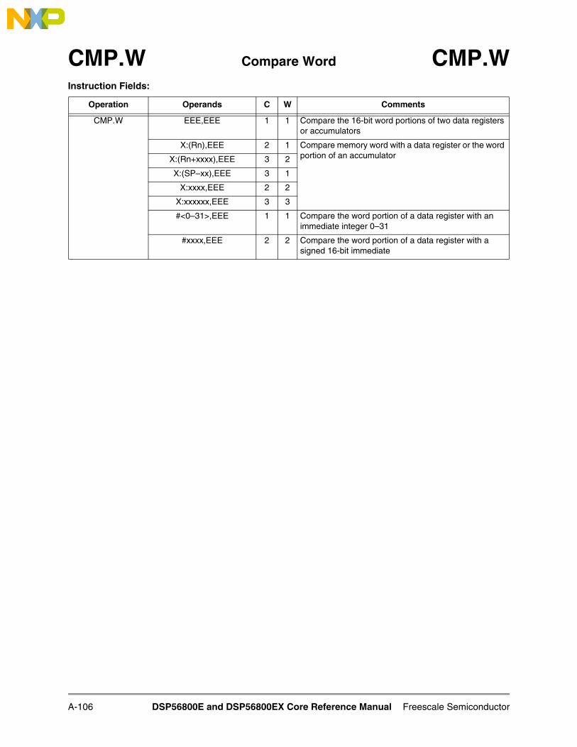
CMP.W Compare Word CMP.WInstruction Fields:
Operation Operands C W Comments
CMP.W EEE,EEE 1 1 Compare the 16-bit word portions of two data registers or accumulators
X:(Rn),EEE 2 1 Compare memory word with a data register or the word portion of an accumulatorX:(Rn+xxxx),EEE 3 2
X:(SP–xx),EEE 3 1
X:xxxx,EEE 2 2
X:xxxxxx,EEE 3 3
#<0–31>,EEE 1 1 Compare the word portion of a data register with an immediate integer 0–31
#xxxx,EEE 2 2 Compare the word portion of a data register with a signed 16-bit immediate
A-106 DSP56800E and DSP56800EX Core Reference Manual Freescale Semiconductor

CMP.W Compare Word CMP.WInstruction Opcodes:
15 12 11 8 7 4 3 0
CMP.W #<0–31>,DD 0 1 0 1 1 1 1 D D 0 0 B B B B B
15 12 11 8 7 4 3 0
CMP.W #<0–31>,FF 0 1 0 0 1 1 0 F F 0 0 B B B B B
15 12 11 8 7 4 3 0
CMP.W #xxxx,DD 0 1 0 1 1 1 1 D D 1 0 0 0 0 0 0
iiiiiiiiiiiiiiii
15 12 11 8 7 4 3 0
CMP.W #xxxx,FF 0 1 0 0 1 1 0 F F 1 0 0 0 0 0 0
iiiiiiiiiiiiiiii
15 12 11 8 7 4 3 0
CMP.W EEE,EEE 0 1 1 1 1 0 E E E a a a 0 1 1 0
15 12 11 8 7 4 3 0
CMP.W X:(Rn),DD 0 1 0 1 1 1 1 D D 1 0 1 R 1 R R
15 12 11 8 7 4 3 0
CMP.W X:(Rn),FF 0 1 0 0 1 1 0 F F 1 0 1 R 1 R R
15 12 11 8 7 4 3 0
CMP.W X:(Rn+xxxx),DD 0 1 0 1 1 1 1 D D 1 0 1 R 0 R R
AAAAAAAAAAAAAAAA
15 12 11 8 7 4 3 0
CMP.W X:(Rn+xxxx),FF 0 1 0 0 1 1 0 F F 1 0 1 R 0 R R
AAAAAAAAAAAAAAAA
15 12 11 8 7 4 3 0
CMP.W X:(SP–xx),DD 0 1 0 1 1 0 1 D D 1 a a a a a a
15 12 11 8 7 4 3 0
CMP.W X:(SP–xx),FF 0 1 0 0 1 0 0 F F 1 a a a a a a
15 12 11 8 7 4 3 0
CMP.W X:xxxx,DD 0 1 0 1 1 1 1 D D 1 0 0 0 1 0 0
AAAAAAAAAAAAAAAA
15 12 11 8 7 4 3 0
CMP.W X:xxxx,FF 0 1 0 0 1 1 0 F F 1 0 0 0 1 0 0
AAAAAAAAAAAAAAAA
Freescale Semiconductor Instruction Set Details A-107

CMP.W Compare Word CMP.WInstruction Opcodes:(continued)
Timing: 1–3 oscillator clock cycle(s)
Memory: 1–3 program word(s)
15 12 11 8 7 4 3 0
CMP.W X:xxxxxx,FF 1 1 1 0 0 A A A 0 A 1 1 A A A A
0 1 0 0 1 1 0 F F 1 0 0 0 1 0 0
AAAAAAAAAAAAAAAA
15 12 11 8 7 4 3 0
CMP.W X:xxxxxx,DD 1 1 1 0 0 A A A 0 A 1 1 A A A A
0 1 0 1 1 1 1 D D 1 0 0 0 1 0 0
AAAAAAAAAAAAAAAA
A-108 DSP56800E and DSP56800EX Core Reference Manual Freescale Semiconductor

CMPA Compare AGU Registers CMPAOperation: Assembler Syntax:
D – S (no parallel move) CMPA S,D (no parallel move)
Description: Compare two AGU address registers by subtracting the source from the destination, and update theCCR based on the result of the subtraction. The result of the subtraction operation is not stored.
Example:
CMPA R0,R1 ; compare R0 and R1
Explanation of Example:Prior to execution, the R0 register contains the value $082473, R1 contains the value $002473, and thestatus register (SR) contains $0300. Execution of the CMPA R0,R1 instruction subtracts R0 from R1and updates the CCR, leaving the registers unchanged.
Condition Codes Affected:
N — Set if bit 23 of the result is setZ — Set if result equals zeroV — Set if overflow has occurred in resultC — Set if a borrow occurs from bit 23 of the result
Instruction Fields:
Instruction Opcodes:
Timing: 1 oscillator clock cycle
Memory: 1 program word
Operation Operands C W Comments
CMPA Rn,Rn 1 1 24-bit compare between two AGU registers
Before Execution
002473R1
After Execution
082473R0
002473R1
0309SR
082473R0
0300SR
LF P4 P3 P2 P1 P0 I1 I0 SZ L E U N Z V C
MR CCR
15 14 13 12 11 10 9 8 7 6 5 4 3 2 1 0
15 12 11 8 7 4 3 0
CMPA Rn,Rn 1 0 0 0 1 1 1 1 n 0 1 n R n R R
Freescale Semiconductor Instruction Set Details A-109

CMPA.W Compare AGU Registers (Word) CMPA.WOperation: Assembler Syntax:
D – S (no parallel move) CMPA.W S,D (no parallel move)
Description: Compare the low-order 16 bits of two AGU address registers by subtracting the source from the des-tination, and update the CCR based on the result of the subtraction. The result of the subtraction oper-ation is not stored.
Usage: This instruction is provided for compatibility with the DSP56800 CMPA instruction, and it should beused when only 16-bit address comparisons are required.
Example:
CMPA.W R0,R1 ; compare R0 and R1
Explanation of Example:Prior to execution, the R0 register contains the value $082473, R1 contains the value $002473, and thestatus register (SR) contains $0300. Execution of the CMPA.W R0,R1 instruction subtracts thelow-order 16 bits of R0 from the low-order 16 bits of R1 and updates the CCR, leaving the registersunchanged. In this case, both address registers are considered equal.
Condition Codes Affected:
N — Set if bit 15 of the result is setZ — Set if result equals zeroV — Set if overflow has occurred in resultC — Set if a borrow occurs from bit 15 of the subtraction
Instruction Fields:
Instruction Opcodes:
Timing: 1 oscillator clock cycle
Memory: 1 program word
Operation Operands C W Comments
CMPA.W Rn,Rn 1 1 16-bit compare between two AGU registers
Before Execution
002473R1
0300SR
After Execution
082473R0
002473R1
0304SR
082473R0
LF P4 P3 P2 P1 P0 I1 I0 SZ L E U N Z V C
MR CCR
15 14 13 12 11 10 9 8 7 6 5 4 3 2 1 0
15 12 11 8 7 4 3 0
CMPA.W Rn,Rn 1 0 0 0 1 1 1 0 n 0 1 n R n R R
A-110 DSP56800E and DSP56800EX Core Reference Manual Freescale Semiconductor

DEBUGEV Generate Debug Event DEBUGEVOperation: Assembler Syntax:
Generate a debugging event DEBUGEV
Description: Generate a debugging event in the Enhanced OnCE module. For more information on the EnhancedOnCE port and hardware debugging support, see the manual for the appropriate DSC device.
Note: This instruction is equivalent to the DSP56800 DEBUG instruction. Programs that are being portedfrom the DSP56800 should use this instruction in place of the DEBUG instruction to remain compat-ible with the DSP56800 behavior.
Condition Codes Affected:No condition codes are affected.
Instruction Fields:
Instruction Opcodes:
Timing: 3 oscillator clock cycles
Memory: 1 program word
Operation Operands C W Comments
DEBUGEV 3 1 Generate a debug event
15 12 11 8 7 4 3 0
DEBUGEV 1 1 1 0 0 1 1 1 0 0 0 0 0 0 1 1
Freescale Semiconductor Instruction Set Details A-111

DEBUGHLT Enter Debug Mode DEBUGHLTOperation: Assembler Syntax:
Enter the debug processing state DEBUGHLT
Description: Enter the debug processing state and wait for Enhanced OnCE port commands, if this state is enabledin the Enhanced OnCE unit. If this state is not enabled, then the processor simply executes two NOPsand continues program execution. For more information on the Enhanced OnCE port and hardware de-bugging support, see the manual for the appropriate DSC device.
Note: This instruction is not compatible with the DSP56800 DEBUG instruction. Please see the DEBUGEVinstruction for information on DSP56800–compatible debugging.
Condition Codes Affected:No condition codes are affected.
Instruction Fields:
Instruction Opcodes:
Timing: 3 oscillator clock cycles
Memory: 1 program word
Operation Operands C W Comments
DEBUGHLT 3 1 Enter debug processing state
15 12 11 8 7 4 3 0
DEBUGHLT 1 1 1 0 0 1 1 1 0 0 0 0 0 0 0 1
A-112 DSP56800E and DSP56800EX Core Reference Manual Freescale Semiconductor

DEC.BP Decrement Byte (Byte Pointer) DEC.BPOperation: Assembler Syntax:
D – 1 → D (no parallel move) DEC.BP D (no parallel move)
Description: Decrement a byte value in memory. The value is internally sign extended to 20 bits before being dec-remented. The low-order 8 bits of the result are stored back to memory. The condition codes are cal-culated based on the 8-bit result, with the exception of the E and U bits, which are calculated based onthe 20-bit result. Absolute addresses are expressed as byte addresses. The result is not affected by thestate of the saturation bit (SA).
Usage: This instruction is typically used when integer data is processed.
Example:
DEC.BP X:$3065 ; decrement the byte at (byte) address $3065
Explanation of Example:Prior to execution, the value at byte address X:$3065 is $00. Execution of the DEC.BP instruction dec-rements this value by one and generates the result, $FF, with a borrow (the carry bit is set). The resultis negative since bit 7 is set. Note that this address is equivalent to the upper byte of word address$1832.
Condition Codes Affected:
E — Set if the extension portion of the 20-bit result is in useU — Set if the 20-bit result is unnormalizedN — Set if bit 7 of the result is setZ — Set if the result is zeroV — Set if overflow has occurred in resultC — Set if a carry (or borrow) occurs from bit 7 of the result
$3064
$3066
$3068
$3062
X Memory
22 11
7 0
77
00 33
558866
ByteAddresses 7
$3064
$3066
$3068
$3062
X Memory
22 11
7 0
77
FF 33
558866
ByteAddresses 70
Before Execution After Execution
0300SR 0319SR
0
LF P4 P3 P2 P1 P0 I1 I0 SZ L E U N Z V C
MR CCR
15 14 13 12 11 10 9 8 7 6 5 4 3 2 1 0
Freescale Semiconductor Instruction Set Details A-113

DEC.BP Decrement Byte (Byte Pointer) DEC.BPInstruction Fields:
Instruction Opcodes:
Timing: 3–4 oscillator clock cycles
Memory: 2–3 program words
Operation Operands C W Comments
DEC.BP X:xxxx 3 2 Decrement byte in memory
X:xxxxxx 4 3
15 12 11 8 7 4 3 0
DEC.BP X:xxxx 0 1 0 0 1 1 1 0 0 1 0 0 0 1 1 0
AAAAAAAAAAAAAAAA
15 12 11 8 7 4 3 0
DEC.BP X:xxxxxx 1 1 1 0 0 A A A 0 A 1 1 A A A A
0 1 0 0 1 1 1 0 0 1 0 0 0 1 1 0
AAAAAAAAAAAAAAAA
A-114 DSP56800E and DSP56800EX Core Reference Manual Freescale Semiconductor

DEC.L Decrement Long DEC.LOperation: Assembler Syntax:
D – 1 → D (no parallel move) DEC.L D (no parallel move)
Description: Decrement a long-word value in a register or memory. When an operand located in memory is operatedon, the low-order 32 bits of the result are stored back to memory. The condition codes are calculatedbased on the 32-bit result. Absolute addresses pointing to long elements must always be even aligned(that is, pointing to the lowest 16 bits).
Usage: This instruction is typically used when integer data is processed.
Example:
DEC.L X:$2000 ; decrement value in location: $2001:2000 by 1
Explanation of Example:Prior to execution, the 32-bit value at location $2001:2000 is $1000:0000. Execution of the DEC.L in-struction subtracts this value by one and generates $0FFF:FFFF. The CCR is updated based on the re-sult of the subtraction.
Condition Codes Affected:
E — Set if the extension portion of the result is in useU — Set if the 32-bit result is unnormalizedN — Set if bit 31 of the result is setZ — Set if the result is zeroV — Set if overflow has occurred in resultC — Set if a carry (or borrow) occurs from bit 31 of the result
$200010000000
$2001$2000
0FFFFFFF
$2001
0301SR 0310SR
Before Execution After ExecutionX Memory X Memory
$1FFF $1FFF
0300SR
8000 8000
LF P4 P3 P2 P1 P0 I1 I0 SZ L E U N Z V C
MR CCR
15 14 13 12 11 10 9 8 7 6 5 4 3 2 1 0
Freescale Semiconductor Instruction Set Details A-115

DEC.L Decrement Long DEC.LInstruction Fields:
Instruction Opcodes:
Timing: 1–4 oscillator clock cycle(s)
Memory: 1–3 program word(s)
Operation Operands C W Comments
DEC.L fff 1 1 Decrement long
X:xxxx 3 2 Decrement long in memory
X:xxxxxx 4 3
15 12 11 8 7 4 3 0
DEC.L X:xxxx 0 1 0 0 1 1 1 0 0 1 0 0 0 1 1 1
AAAAAAAAAAAAAAAA
15 12 11 8 7 4 3 0
DEC.L X:xxxxxx 1 1 1 0 0 A A A 0 A 1 1 A A A A
0 1 0 0 1 1 1 0 0 1 0 0 0 1 1 1
AAAAAAAAAAAAAAAA
15 12 11 8 7 4 3 0
DEC.L fff 0 1 1 1 0 0 f f f 0 0 1 1 0 1 1
A-116 DSP56800E and DSP56800EX Core Reference Manual Freescale Semiconductor

DEC.W Decrement Word DEC.WOperation: Assembler Syntax:
D – 1 → D (one parallel move) DEC.W D (one parallel move)D – 1 → D (no parallel move) DEC.W D (no parallel move)
Description: Decrement a 16-bit destination by one. If the destination is an accumulator, only the EXT and MSPportions of the accumulator are used and the LSP remains unchanged. The condition codes are calcu-lated based on the 16-bit result (or on the 20-bit result for accumulators).
Usage: This instruction is typically used when integer data is processed.
Example:
DEC.W A X:(R2)+,X0 ; Decr the 20 MSBs of A, update R2,X0
Explanation of Example:Prior to execution, the 36-bit A accumulator contains the value $0:0001:0033. Execution of theDEC.W instruction decrements by one the upper 20 bits of the A accumulator and sets the zero bit inthe CCR. A new value is read in parallel and stored in register X0; the address register R2 is post-in-cremented.
Condition Codes Affected:
SZ — Set according to the standard definition of the SZ bit (parallel move)L — Set if limiting (parallel move) or overflow has occurred in resultE — Set if the extension portion of the result is in useU — Set if result is unnormalizedN — Set if bit MSB of the result is setZ — Set if the result is zero (20 MSB for accumulator destinations)V — Set if overflow has occurred in resultC — Set if a carry (or borrow) occurs from bit 15 of the result (bit 35 for accumulators)
Note: When the destination is one of the four accumulators, condition code calculations follow the rules for20-bit arithmetic; otherwise, the rules for 16-bit arithmetic apply.
A Before Execution
003300010
A2 A1 A0
A After Execution
003300000
A2 A1 A0
0300SR 0314SR
LF P4 P3 P2 P1 P0 I1 I0 SZ L E U N Z V C
MR CCR
15 14 13 12 11 10 9 8 7 6 5 4 3 2 1 0
Freescale Semiconductor Instruction Set Details A-117

DEC.W Decrement Word DEC.WInstruction Fields:
Parallel Moves:
Operation Operands C W Comments
DEC.W EEE 1 1 Decrement word.
X:(Rn) 3 1 Decrement word in memory using appropriate address-ing mode.X:(Rn+xxxx) 4 2
X:(SP–xx) 4 1
X:xxxx 3 2
X:xxxxxx 4 3
Data ALU Operation Parallel Memory Move
Operation Operands Source Destination1
1.The case where the destination of the data ALU operation is the same register as the destination of the par-allel read operation is not allowed. Memory writes are allowed in this case.
DEC.W2
2.This instruction occupies only 1 program word and executes in 1 cycle for every addressing mode.
F X:(Rj)+X:(Rj)+N
X0Y1Y0ABCA1B1
X0Y1Y0ABCA1B1
X:(Rj)+X:(Rj)+N
A-118 DSP56800E and DSP56800EX Core Reference Manual Freescale Semiconductor

DEC.W Decrement Word DEC.WInstruction Opcodes:
Timing: 1–4 oscillator clock cycle(s)
Memory: 1–3 program word(s)
15 12 11 8 7 4 3 0
DEC.W EEE 0 1 1 1 0 0 E E E 0 0 0 1 0 1 1
15 12 11 8 7 4 3 0
DEC.W F GGG,X:<ea_m> 0 0 0 0 0 G G G F 0 0 1 0 m R R
15 12 11 8 7 4 3 0
DEC.W F X:<ea_m>,GGG 0 0 1 0 0 G G G F 0 0 1 0 m R R
15 12 11 8 7 4 3 0
DEC.W X:(Rn) 0 1 0 0 1 1 1 0 0 1 0 1 R 1 R R
15 12 11 8 7 4 3 0
DEC.W X:(Rn+xxxx) 0 1 0 0 1 1 1 0 0 1 0 1 R 0 R R
AAAAAAAAAAAAAAAA
15 12 11 8 7 4 3 0
DEC.W X:(SP–xx) 0 1 0 0 1 0 1 0 0 1 a a a a a a
15 12 11 8 7 4 3 0
DEC.W X:xxxx 0 1 0 0 1 1 1 0 0 1 0 0 0 1 0 0
AAAAAAAAAAAAAAAA
15 12 11 8 7 4 3 0
DEC.W X:xxxxxx 1 1 1 0 0 A A A 0 A 1 1 A A A A
0 1 0 0 1 1 1 0 0 1 0 0 0 1 0 0
AAAAAAAAAAAAAAAA
Freescale Semiconductor Instruction Set Details A-119

DECA Decrement AGU Register DECAOperation: Assembler Syntax:
D – 1 → D (no parallel move) DECA D (no parallel move)
Description: Decrement a value in an AGU pointer register. The full 24-bit value of the pointer register is used whendecrementing.
Usage: This instruction can be used to step backwards through a memory buffer.
Example:
DECA R0 ; decrement R0
Explanation of Example:Prior to execution, the R0 register contains $002222. Execution of the DECA R0 instruction causesthe value in R0 to be reduced by one, and the result ($002221) is stored back in R0.
Condition Codes Affected:The condition codes are not modified by this instruction.
Instruction Fields:
Instruction Opcodes:
Timing: 1 oscillator clock cycle
Memory: 1 program word
Operation Operands C W Comments
DECA Rn 1 1 Decrement AGU register by one
Before Execution After Execution
002222R0 002221R0
15 12 11 8 7 4 3 0
DECA Rn 1 0 0 0 0 1 0 0 1 0 1 1 R 0 R R
A-120 DSP56800E and DSP56800EX Core Reference Manual Freescale Semiconductor

DECA.L Decrement Long in AGU Register DECA.LOperation: Assembler Syntax:
D – 2 → D (no parallel move) DECA.L D (no parallel move)
Description: Decrement a value in an AGU pointer register by two. The full 24-bit value of the pointer register isused when decrementing.
Usage: This instruction is used to step backwards through a memory buffer that is composed of long-word val-ues. Since each long word consists of 2 words, this instruction can be used to step through a buffer byevery other word.
Example:
DECA.L R0 ; decrement R0 by 2
Explanation of Example:Prior to execution, the R0 register contains $002222. Execution of the DECA.L R0 instruction causesthe value in the R0 to be reduced by two, and the result ($002220) is stored back in R0.
Condition Codes Affected:The condition codes are not modified by this instruction.
Instruction Fields:
Instruction Opcodes:
Timing: 1 oscillator clock cycle
Memory: 1 program word
Operation Operands C W Comments
DECA.L Rn 1 1 Decrement AGU register by two
Before Execution After Execution
002222R0 002220R0
15 12 11 8 7 4 3 0
DECA.L Rn 1 0 0 0 0 1 0 0 1 0 1 1 R 1 R R
Freescale Semiconductor Instruction Set Details A-121

DECTSTA Decrement and Test AGU Register DECTSTAOperation: Assembler Syntax:
D – 1 → D (no parallel move) DECTSTA D (no parallel move)D – 0
Description: Decrement a value in an AGU pointer register and then compare the result to zero, updating the con-dition codes based on the comparison. The full 24-bit value of the pointer register is used when decre-menting.
Usage: This instruction can be used to step backwards through a memory buffer, testing to see that the pointeris still valid after each step.
Example:
DECTSTA R0 ; decrement R0 and then compare to 0
Explanation of Example:Prior to execution, the R0 register contains $002222. Execution of the DECTSTA R0 instruction caus-es the value in R0 to be reduced by one, and the result ($002221) is stored back in R0. The updatedvalue in R0 is then compared with zero, and the CCR is updated accordingly.
Condition Codes Affected:
N — Set if bit 23 of the result is setZ — Set if all bits in the result are zeroV — Set if overflow has occurred in resultC — Set if a borrow occurs from bit 23 of the result
Instruction Fields:
Instruction Opcodes:
Timing: 1 oscillator clock cycle
Memory: 1 program word
Operation Operands C W Comments
DECTSTA Rn 1 1 Decrement and test AGU register
Before Execution After Execution
002222R0 002221R0
0308SR 0300SR
LF P4 P3 P2 P1 P0 I1 I0 SZ L E U N Z V C
MR CCR
15 14 13 12 11 10 9 8 7 6 5 4 3 2 1 0
15 12 11 8 7 4 3 0
DECTSTA Rn 1 0 0 0 0 1 0 0 1 0 1 0 R 1 R R
A-122 DSP56800E and DSP56800EX Core Reference Manual Freescale Semiconductor

DIV Divide Iteration DIVOperation: Assembler Syntax:
(see following figure) DIV S,D (no parallel move)
Description: This instruction is a divide iteration that is used to calculate 1 bit of the result of a division. After thecorrect number of iterations, this instruction will divide the destination operand (D)—dividend or nu-merator—by the source operand (S)—divisor or denominator—and store the result in the destinationaccumulator. The 32-bit dividend must be a positive value that is correctly sign extended to 36 bits andthat is stored in the full 36-bit destination accumulator. The 16-bit divisor is a signed value and isstored in the source operand. (The division of signed numbers is handled using the techniques docu-mented in Section 5.3.4, “Division,” on page 5-21.) This instruction can be used for both integer andfractional division. Each DIV iteration calculates 1 quotient bit using a non-restoring division algo-rithm (see the description that follows). After the execution of the first DIV instruction, the destinationoperand holds both the partial remainder and the formed quotient. The partial remainder occupies thehigh-order portion of the destination accumulator and is a signed fraction. The formed quotient occu-pies the low-order portion of the destination accumulator (A0 or B0, C0, or D0) and is a positive frac-tion. One bit of the formed quotient is shifted into the LSB of the destination accumulator at the startof each DIV iteration. The formed quotient is the true quotient if the true quotient is positive. If the truequotient is negative, the formed quotient must be negated. For fractional division, valid results are ob-tained only when |D| < |S|. This condition ensures that the magnitude of the quotient is less than one(that is, it is fractional) and precludes division by zero.
The DIV instruction calculates 1 quotient bit based on the divisor and the previous partial remainder.To produce an N-bit quotient, the DIV instruction is executed N times, where N is the number of bitsof precision that is desired in the quotient (1 < N < 16). Thus, for a full-precision (16-bit) quotient,16 DIV iterations are required. In general, executing the DIV instruction N times produces an N-bitquotient and a 32-bit remainder, which has (32 – N) bits of precision and whose N MSBs are zeros.The partial remainder is not a true remainder and must be corrected (due to the non-restoring nature ofthe division algorithm) before it may be used. Therefore, once the divide is complete, it is necessaryto reverse the last DIV operation and restore the remainder to obtain the true remainder. The result isnot affected by the state of the saturation bit (SA).
The DIV instruction uses a non-restoring division algorithm that consists of the following operations:
1. Compare the source and destination operand sign bits. An exclusive OR operation is performed onbit 35 of the destination operand and bit 15 of the source operand.
2. Shift the partial remainder and the quotient. The 36-bit destination accumulator is shifted 1 bit to theleft. C is moved into the LSB (bit 0) of the accumulator.
D1 + S D1
D0D2 D1
C;
D[35] ⊕ S[15] = 1If
Then
D1 – S D1
D0D2 D1
C;
Else
Freescale Semiconductor Instruction Set Details A-123

DIV Divide Iteration DIV3. Calculate the next quotient bit and the new partial remainder. The 16-bit source operand (signed
divisor) is either added to or subtracted from the MSP of the destination accumulator (FF1 portion),and the result is stored back into the MSP of the destination accumulator. If the result of the exclusiveOR operation in the first step was one (that is, the sign bits were different), the source operand S isadded to the accumulator. If the result of the exclusive OR operation was zero (that is, the sign bitswere the same), the source operand S is subtracted from the accumulator. Due to the automatic signextension of the 16-bit signed divisor, the addition or subtraction operation correctly sets the C bitwith the next quotient bit.
Usage: The DIV iteration instruction can be used in one of several different division algorithms, depending onthe needs of an application. Section 5.3.4, “Division,” on page 5-21 shows the correct usage of this in-struction for fractional and integer division routines, discusses in detail issues related to division, andprovides several examples. The division routine is greatly simplified if both operands are positive, orif it is not necessary also to calculate a remainder.
Condition Codes Affected:
L — Set if overflow bit V is setV — Set if the MSB of the destination operand (bit 35 for an accumulator,
bit 35 after sign extension for the Y register) is changed as a resultof the instruction’s left shift operation; otherwise, V is cleared
C — Set if MSB of the result is zero (bit 35 for an accumulator,bit 35 after sign extension for the Y register)
Example:
DIV Y0,A ; divide A by Y0
Explanation of Example:This example shows only a single iteration of the division instruction. Please refer to Section 5.3.4,“Division,” on page 5-21 for a complete description of a division algorithm.
LF P4 P3 P2 P1 P0 I1 I0 SZ L E U N Z V C
MR CCR
15 14 13 12 11 10 9 8 7 6 5 4 3 2 1 0
Before Execution
000007020
A2 A1 A0
0301SR
After Execution
00010E000
A2 A1 A0
0301SR
00042000
Y1 Y0
00042000
Y1 Y0
A-124 DSP56800E and DSP56800EX Core Reference Manual Freescale Semiconductor

DIV Divide Iteration DIVInstruction Fields:
Instruction Opcodes:
Timing: 1 oscillator clock cycle
Memory: 1 program word
Operation Operands C W Comments
DIV FFF1,fff 1 1 Divide iteration
15 12 11 8 7 4 3 0
DIV FFF1,fff 0 1 1 1 1 0 f f f c c c 1 1 1 1
Freescale Semiconductor Instruction Set Details A-125

DO Start Hardware DO Loop DOOperation: Assembler Syntax:
HWS0 → HWS1; DO S,DLC → LC2LA → LA2LF → NLPC → HWS0S → LCD → LA1 → LF
Operation When Loop Completes (End-of-Loop Processing):
If NL == 1LC2 → LC, LA2 → LA
HWS1 → HWS0NL → LF0 → NL
Description: Begin a hardware DO loop that is to be repeated for the number of times specified in the instruction’ssource operand, and whose range of execution is terminated by the destination operand. The sourceoperand specifies the loop count and can be either an immediate 6-bit unsigned value or an on-chipregister value, and the destination operand is a 16- or 21-bit absolute address. No overhead other thanthe execution of the DO instruction is required to set up this loop. When a DO loop is executed, theinstructions are actually fetched each time through the loop. Therefore, a DO loop can be interrupted.
The DO instruction performs hardware looping on a single instruction or a block of instructions. DOloops can be nested up to two deep, accelerating more complex algorithms.
Example 1:DO #40,END_CPY ; Set up hardware DO loopMOVE.L X:(R0)+,A ; Copy a 32-bit memory locationMOVE.L A10,X:(R1)+ ;
END_CPY
Explanation of Example:This example copies a block of forty 32-bit memory locations from one area of memory to another.
When a hardware DO loop is initiated, the following events occur:
1. When the DO instruction is executed, the contents of the LC register are copied to the LC2 register, and LC is loaded with the loop count that the instruction specifies.
2. The old contents of the LA register are copied to the LA2 register, and the LA register is loaded with the address of the last instruction word in the loop. If a 16-bit address is specified, the upper 8 bits of LA are cleared.
3. The address of the first instruction in the program loop (top-of-loop address) is pushed onto the hardware stack. This push sets the LF bit and updates the NL bit, as occurs with any hardware stack push.
Instructions in the loop are then executed. The address of each instruction is compared to the value inLA to see if it is the last instruction in the loop. When the end of the loop is reached, the loop countregister is checked to see if the loop should be repeated. If the value in LC is greater than one, LC isdecremented and the loop is re-started from the top. If LC is equal to one, the loop has been executedfor the proper number of times and should be exited.
When a hardware loop ends, the hardware stack is popped (and the popped value is discarded), the LA2register is copied to LA, the LC2 register is copied to LC, and the NL bit in the operating mode registeris copied to the LF bit. Instruction execution then continues at the address that immediately follows theend-of-loop address.
A-126 DSP56800E and DSP56800EX Core Reference Manual Freescale Semiconductor

DO Start Hardware DO Loop DOExplanation of Example:(continued)
One hardware stack location is used for each nested DO or DOSLC loop. Thus, a two-deep hardwarestack allows for a maximum of two nested loops. The REP instruction does not use the hardware stack,so repeat loops can be nested within DO loops.
Example 2:MOVE.W #0,X0...DO X0,END_CPY ; Loop count is zero upon entryMOVE.L X:(R0)+,A ; Copy a 32-bit memory locationMOVE.L A10,X:(R1)+ ;
END_CPY
Explanation of Example:A loop count of zero is specified, so the instructions in the body of the loop are skipped, and executioncontinues with the instruction immediately following the loop body.
Note that an immediate loop count of zero for the DO instruction is not allowed and will be rejectedby the assembler. A loop count of zero can only be specified by using a register that is loaded with zeroas the argument to the DO instruction, or by placing a zero in the LC register and executing DOSLC.
A DO loop normally terminates when the body of the loop has been executed for the specified numberof times (the end of the loop has been reached, and LC is one). Alternately, a DO loop terminates if thecount specified is zero, which causes the body of the loop to be skipped entirely.
When the inner loop of a nested loop terminates naturally, the LA2 and LC2 registers are copied intothe LA and LC registers, respectively, restoring these two registers with their values for the outer loop.A loop is determined to be a nested inner loop if the OMR’s NL bit is set. If the NL bit is not set, theLA and LC registers are not modified when a loop is terminated or skipped.
If it is necessary to terminate a DO loop early, use one of the techniques discussed in Section 8.5.4.1,“Allowing Current Block to Finish and Then Exiting,” on page 8-20 and Section 8.5.6.2, “Nesting aDO Loop Within a DO Loop,” on page 8-22.
During the end-of-loop processing, the NL bit is written into the LF, and the NL bit is cleared. Thecontents of the second HWS location (HWS1) are written into the first HWS location (HWS0). Instruc-tion fetches now continue at the address of the instruction that follows the last instruction in the DOloop.
DO loops can also be nested as shown in Section 8.5.6, “Nested Hardware Looping,” on page 8-22.When DO loops are nested, the end-of-loop addresses must also be nested and are not allowed to beequal. The assembler generates an error message when DO loops are improperly nested.
Note: The assembler calculates the end-of-loop address that is to be loaded into LA by subtracting one fromthe absolute address specified in the destination operand. This process occurs to accommodate the casein which the last instruction in the DO loop is a multiple-word instruction. Thus, the end-of-loop ab-solute address in the source code must represent the address of the instruction after the last instructionin the loop.
The LF is cleared by a hardware reset.
Note: Any data dependencies due to pipelining also apply to the pair of instructions formed by the last in-struction in the DO loop and the first instruction of the DO loop.
Freescale Semiconductor Instruction Set Details A-127

DO Start Hardware DO Loop DOExample 3:
DO #cnt1,END ; begin DO loopMOVE.W X:(R0),AREP #cnt2 ; nested REP loopASL A ; repeat this instructionMOVE.W A,X:(R0)+ ; last instruction in DO loop
END : ; (outside DO loop)
Explanation of Example:This example illustrates a DO loop with a REP loop nested within the DO loop. In this example, “cnt1”values are fetched from memory; each value is left shifted by “cnt2” counts and is stored back in mem-ory. The DO loop executes “cnt1” times while the ASL instruction inside the REP loop executes for anumber of times equal to “cnt1” × “cnt2.” The END label is located at the first instruction past the endof the DO loop, as mentioned previously.
Condition Codes Affected:
LF — Set when a DO loop is in progressL — Set if data limiting occurred
Restrictions: Refer to Section 10.4, “Pipeline Dependencies and Interlocks,” on page 10-26.
LF * * * * * I1 I0 SZ L E U N Z V C
MR CCR
15 14 13 12 11 10 9 8 7 6 5 4 3 2 1 0
A-128 DSP56800E and DSP56800EX Core Reference Manual Freescale Semiconductor

DO Start Hardware DO Loop DOInstruction Fields:
Instruction Opcodes:
Timing: 3–8 oscillator clock cycles
Memory: 2–3 program words
Operation Operands C W Comments
DO #<1–63>,<ABS16> 3 2 At least 2 instruction words in the loop (t = 0 in the opcode field).
#<1–63>,<ABS21> 4 3
#<1–63>,<ABS16> 5 2 Only 1 instruction word in the loop (t = 1 in the opcode field).
#<1–63>,<ABS21> 6 3
DDDDD,<ABS16> 7 2 If LC value is zero, body of loop is skipped (adds 2 instruction cycles).When looping with a value in an accumulator, use A1, B1, C1, or D1 to avoid saturation when reading the accumulator.Any DDDDD register is allowed except C2, D2, C0, D0,C, D, Y, M01, N3, LA, LA2, LC, LC2, SR, OMR, and HWS.
DDDDD,<ABS21> 8 3
Note: The immediate value of zero is not allowed.
15 12 11 8 7 4 3 0
DO #<1–63>,<ABS16> 1 1 1 0 1 0 0 t 0 0 B B B B B B
AAAAAAAAAAAAAAAA
15 12 11 8 7 4 3 0
DO #<1–63>,<ABS21> 1 1 1 0 0 A A A 0 A 1 1 A A A A
1 1 1 0 1 0 0 t 0 0 B B B B B B
AAAAAAAAAAAAAAAA
15 12 11 8 7 4 3 0
DO DDDDD,<ABS16> 1 1 1 0 1 0 1 1 0 0 0 d d d d d
AAAAAAAAAAAAAAAA
15 12 11 8 7 4 3 0
DO DDDDD,<ABS21> 1 1 1 0 0 A A A 0 A 1 1 A A A A
1 1 1 0 1 0 1 1 0 0 0 d d d d d
AAAAAAAAAAAAAAAA
Freescale Semiconductor Instruction Set Details A-129

DOSLC DO Loop with Value in LC DOSLCOperation: Assembler Syntax:
HWS0 → HWS1; DOSLC DLA → LA2LF → NLPC → HWS0D → LA1 → LF
Operation When Loop Completes (End-of-Loop Processing):
If NL == 1LC2 → LC, LA2 → LA
HWS1 → HWS0NL → LF0 → NL
Description: Begin a hardware DO loop that is to be repeated for the number of times specified in the loop counter(LC) register. The value of LC must be loaded prior to executing this instruction. If the value in LC iszero or negative, the instructions in the body of the loop are skipped. The destination operand D canbe a 16- or 21-bit absolute address. See the section on the DO instruction for more information on hard-ware looping.
Example:
MOVEU.W #count,LC ; load LC register...DOSLC END ; begin DO loop with value in LCMOVE.W X:(R0),ANEG A ; negate value from bufferMOVE.W A,X:(R0)+ ; last instruction in DO loop
END : ; (outside DO loop)
Explanation of Example:This example illustrates a DO loop with a pre-existing value for LC. For a number of words in the buff-er equal to “count,” the loop reads word values from a buffer in memory, negates them, and writes thevalues back. The END label is located at the first instruction past the end of the DO loop.
Condition Codes Affected:
LF — Set when a DO loop is in progress
Restrictions:Refer to Section 10.4, “Pipeline Dependencies and Interlocks,” on page 10-26.
LF * * * * * I1 I0 SZ L E U N Z V C
MR CCR
15 14 13 12 11 10 9 8 7 6 5 4 3 2 1 0
A-130 DSP56800E and DSP56800EX Core Reference Manual Freescale Semiconductor

DOSLC DO Loop with Value in LC DOSLCInstruction Fields:
Instruction Opcodes:
Timing: 3–4 oscillator clock cycles
Memory: 2–3 program words
Operation Operands C W Comments
DOSLC <ABS16> 3 2 If LC ≤ 0, the body of the loop is skipped, adding 3 additional cycles.
A minimum of 2 instruction words is required in the loop. The assembler will generate an error if the loop body is less than 2 words.
<ABS21> 4 3
15 12 11 8 7 4 3 0
DOSLC <ABS16> 1 1 1 0 0 1 1 1 0 0 0 1 1 0 0 1
AAAAAAAAAAAAAAAA
15 12 11 8 7 4 3 0
DOSLC <ABS21> 1 1 1 0 0 A A A 0 A 1 1 A A A A
1 1 1 0 0 1 1 1 0 0 0 1 1 0 0 1
AAAAAAAAAAAAAAAA
Freescale Semiconductor Instruction Set Details A-131

ENDDO End Current DO Loop ENDDOOperation: Assembler Syntax:
If NL == 1 ENDDOLC2 → LC, LA2 → LA
HWS1 → HWS0NL → LF0 → NL
Description: Terminate the current hardware DO loop immediately. Normally, a hardware DO loop is terminatedwhen the last instruction of the loop is executed and the current LC equals one, but this instruction canterminate a loop before normal completion. If the value of the current DO LC is needed, it must be readbefore the execution of the ENDDO instruction. Initially, the LF is restored from the NL bit, and thetop-of-loop address is purged from the HWS. The contents of the second HWS location are written intothe first HWS location, and the NL bit is cleared.
Example:
DO Y0,ENDLP ; execute loop ending at ENDLP for (Y0) times
:MOVE.W LC,A ; get current value of loop counter (LC)CMP Y1,A ; compare loop counter with value in Y1JNE CONTINU ; go to ONWARD if LC not equal to Y1ENDDO ; LC equal to Y1, restore all DO regis-
tersJMP ENDLP ; go to NEXT
CONTINU : ; LC not equal to Y1, continue DO loop: ; (last instruction in DO loop)
ENDLP MOVE.W #$1234,X0 ; (first instruction AFTER DO loop)
Explanation of Example:This example illustrates the use of the ENDDO instruction to terminate the current DO loop. The valueof the LC is compared with the value in the Y1 register to determine if execution of the DO loop shouldcontinue. The ENDDO instruction updates certain program controller registers but does not automat-ically jump past the end of the DO loop. Thus, if this action is desired, a JMP or BRA instruction (suchas JMP NEXT) must be included after the ENDDO instruction to transfer program control to the firstinstruction past the end of the DO loop.
Note: The ENDDO instruction updates the program controller registers appropriately but does not automat-ically jump past the end of the loop. This must be done explicitly by the programmer if it is desired.
Restrictions:Refer to Section 10.4, “Pipeline Dependencies and Interlocks,” on page 10-26.
Condition Codes Affected:
The condition codes are not affected by this instruction.
A-132 DSP56800E and DSP56800EX Core Reference Manual Freescale Semiconductor

ENDDO End Current DO Loop ENDDOInstruction Fields:
Instruction Opcodes:
Timing: 1 oscillator clock cycle
Memory: 1 program word
Operation Operands C W Comments
ENDDO 1 1 Remove one value from the hardware stack and update the NL and LF bits appropriately
Note: Does not branch to the end of the loop
15 12 11 8 7 4 3 0
ENDDO 1 0 0 0 1 1 1 1 0 0 0 1 1 0 1 1
Freescale Semiconductor Instruction Set Details A-133

EOR.L Logical Exclusive OR Long EOR.LOperation: Assembler Syntax:
S ⊕ D→ D (no parallel move) EOR.L FFF,fff (no parallel move)S ⊕ D → D (one parallel move) EOR.L C,F (one parallel move)
where ⊕ denotes the logical exclusive OR operator
Description: Perform a logical exclusive OR operation on the source operand with the destination operand, and storethe result in the destination. This instruction is a 32-bit operation. If the destination is a 36-bit accumu-lator, the exclusive OR operation is performed on the source with bits 31–0 of the accumulator. Theremaining bits of the destination accumulator are not affected. If the source is a 16-bit register, theEOR.L operation is performed on the source and bits 31–16 of the destination. The other bits of thedestination remain unchanged. The result is not affected by the state of the saturation bit (SA).
Usage: This instruction is used for the logical exclusive OR of two registers. If an exclusive OR of a 16-bitimmediate value with a register or memory location is desired, the EORC instruction is appropriate.
Example:
EOR.L Y,B ;Exclusive OR of Y with B10
Explanation of Example:Prior to execution, the 32-bit Y register contains the value $FF00:FF00, and the 36-bit B accumulatorcontains the value $5:5555:CC89. The EOR.L Y,B instruction performs a logical exclusive OR op-eration on the 32-bit value in the Y register with bits 31–0 of the B accumulator (B10) and stores the36-bit result in the B accumulator. The the extension portion (B2) is not affected by the operation.
Condition Codes Affected:
N — Set if bit 31 of accumulator result or the MSB of the register result is setZ — Set if bits 31–0 of accumulator result or all bits of the register result are zeroV — Always cleared
Before Execution
CC8955555
B2 B1 B0
After Execution
3389AA555
B2 B1 B0
FF00FF00
Y1 Y0
FF00FF00
Y1 Y0
030FSR 0309SR
LF P4 P3 P2 P1 P0 I1 I0 SZ L E U N Z V C
MR CCR
15 14 13 12 11 10 9 8 7 6 5 4 3 2 1 0
A-134 DSP56800E and DSP56800EX Core Reference Manual Freescale Semiconductor

EOR.L Logical Exclusive OR Long EOR.LInstruction Fields:
Parallel Moves:
Instruction Opcodes:
Timing: 1 oscillator clock cycle
Memory: 1 program word
Operation Operands C W Comments
EOR.L FFF,fff 1 1 32-bit exclusive OR (XOR).
Data ALU Operation Parallel Memory Move
Operation Operands Source Destination1
1.The case where the destination of the data ALU operation is the same register as the destination of the par-allel read operation is not allowed. Memory writes are allowed in this case.
EOR.L2
2.This instruction occupies only 1 program word and executes in 1 cycle for every addressing mode.
C,F X:(Rj)+X:(Rj)+N
X0Y1Y0ABCA1B1
X0Y1Y0ABCA1B1
X:(Rj)+X:(Rj)+N
15 12 11 8 7 4 3 0
EOR.L C,F GGG,X:<ea_m> 0 0 0 1 1 G G G F 0 1 0 0 m R R
15 12 11 8 7 4 3 0
EOR.L C,F X:<ea_m>,GGG 0 0 1 1 1 G G G F 0 1 0 0 m R R
15 12 11 8 7 4 3 0
EOR.L FFF,fff 0 1 1 1 1 0 f f f b b b 1 1 1 0
Freescale Semiconductor Instruction Set Details A-135

EOR.W Logical Exclusive OR Word EOR.WOperation: Assembler Syntax:
S ⊕ D → D (no parallel move) EOR.W S,D (no parallel move)S ⊕ D[31:16] → D[31:16] (no parallel move) EOR.W S,D (no parallel move)
where ⊕ denotes the logical exclusive OR operator
Description: Perform a logical exclusive OR operation on the source operand (S) with the destination operand (D),and store the result in the destination. This instruction is a 16-bit operation. If the destination is a 36-bitaccumulator, the exclusive OR operation is performed on the source with bits 31–16 of the accumula-tor. The remaining bits of the destination accumulator are not affected. The result is not affected by thestate of the saturation bit (SA).
Usage: This instruction is used for the logical exclusive OR of two registers. If an exclusive OR of a 16-bitimmediate value with a register or memory location is desired, the EORC instruction is appropriate.
Example:
EOR.W Y1,B ;Exclusive OR of Y1 with B1
Explanation of Example:Prior to execution, the 16-bit Y1 register contains the value $FF00, and the 36-bit B accumulator con-tains the value $5:5555:6789. The EOR.W Y1,B instruction performs a logical exclusive OR opera-tion on the 16-bit value in the Y1 register with bits 31–16 of the B accumulator (B1) and stores the36-bit result in the B accumulator. The lower word of the accumulator (B0) and the extension byte (B2)are not affected by the operation.
Condition Codes Affected:
N — Set if bit 31 of accumulator result or MSB of register result is setZ — Set if bits 31–16 of accumulator result or all bits of register result are zeroV — Always cleared
Before Execution
678955555
B2 B1 B0
After Execution
6789AA555
B2 B1 B0
8000FF00
Y1 Y0
8000FF00
Y1 Y0
030FSR 0309SR
LF P4 P3 P2 P1 P0 I1 I0 SZ L E U N Z V C
MR CCR
15 14 13 12 11 10 9 8 7 6 5 4 3 2 1 0
A-136 DSP56800E and DSP56800EX Core Reference Manual Freescale Semiconductor

EOR.W Logical Exclusive OR Word EOR.WInstruction Fields:
Instruction Opcodes:
Timing: 1 oscillator clock cycle
Memory: 1 program word
Operation Operands C W Comments
EOR.W EEE,EEE 1 1 16-bit exclusive OR (XOR)
15 12 11 8 7 4 3 0
EOR.W EEE,EEE 0 1 1 1 1 0 E E E a a a 1 0 1 0
Freescale Semiconductor Instruction Set Details A-137

EORC Logical Exclusive OR Immediate EORCOperation: Assembler Syntax:
#xxxx ⊕ X:<ea> → X:<ea>(no parallel move) EORC #iiii,X:<ea> (no parallel move)#xxxx ⊕ D → D(no parallel move) EORC #iiii,D (no parallel move)
where ⊕ denotes the logical exclusive OR operator
Implementation Note:This instruction is implemented by the assembler as an alias to the BFCHG instruction, and it uses the16-bit immediate value as the bit mask. This instruction will dis-assemble as a BFCHG instruction.
Description: Perform a logical exclusive OR operation on a 16-bit immediate data value with the destination oper-and (D), and store the results back into the destination. C is also modified as described in “ConditionCodes Affected.” This instruction performs a read-modify-write operation on the destination and re-quires two destination accesses.
Example:
EORC #$0FF0,X:$5000; Exclusive OR with immediate data
Explanation of Example:Prior to execution, the 16-bit X memory location X:$5000 contains the value $5555. Execution of theinstruction tests the state of bits 4–11 in X:$5000, does not set C (because all of the selected bits werenot set), and then complements the bits.
Condition Codes Affected:
For destination operand SR:All SR bits except bits 14–10 are updated with values from the bitfield unit. Bits 14–10 of the mask operand must be cleared.
For other destination operands:L — Set if data limiting occurred during 36-bit source moveC — Set if all bits specified by the mask are set
Cleared if at least 1 bit specified by the mask is not set
Note: If all bits in the mask are cleared, the instruction executes two NOPs and sets the C bit.
Instruction Fields:Refer to the section on the BFCHG instruction for legal operand and timing information.
Before Execution
5555X:$5000
0300SR
After Execution
5AA5X:$5000
0300SR
LF P4 P3 P2 P1 P0 I1 I0 SZ L E U N Z V C
MR CCR
15 14 13 12 11 10 9 8 7 6 5 4 3 2 1 0
A-138 DSP56800E and DSP56800EX Core Reference Manual Freescale Semiconductor

FRTID Delayed Return from Fast Interrupt FRTIDOperation: Assembler Syntax:
Swap shadow registers, then FRTIDreturn from fast interrupt service routine
Description: Refer to Section 9.3.2.2, “Fast Interrupt Processing,” on page 9-6.
Condition Codes Affected:
All bits are set according to the value removed from the stack
Restrictions:Refer to Section 4.3.2, “Delayed Instruction Restrictions,” on page 4-14.
Instruction Fields:
Instruction Opcodes:
Timing: 2 oscillator clock cycles
Memory: 1 program word
Operation Operands C W Comments
FRTID 2 1 Delayed return from interrupt, restoring 21-bit PC and SR from the stack; must fill 2 word slots
LF P4 P3 P2 P1 P0 I1 I0 SZ L E U N Z V C
MR CCR
15 14 13 12 11 10 9 8 7 6 5 4 3 2 1 0
15 12 11 8 7 4 3 0
FRTID 1 1 1 0 0 1 1 1 0 0 0 1 1 0 1 0
Freescale Semiconductor Instruction Set Details A-139

ILLEGAL Illegal Instruction Interrupt ILLEGALOperation: Assembler Syntax:
Begin illegal instruction exception routine ILLEGAL (no parallel move)
Description: Normal instruction execution is suspended, and illegal instruction exception processing is initiated.The interrupt priority level bits (I1 and I0) are set to 11 in the status register. The purpose of the illegalinterrupt is to force the DSC into an illegal instruction exception for test purposes. Executing an ILLEGAL instruction is a fatal error; the exception routine should indicate this condition and cause thesystem to be re-started.
If the ILLEGAL instruction is in a DO loop at the LA and the instruction at the LA – 1 is being inter-rupted, then LC will be decremented twice. This situation is due to the same mechanism that causesLC to be decremented twice if JSR, REP, and so on are located at the LA.
Since REP is uninterruptable, the result of repeating an ILLEGAL instruction is that the interrupt isnot taken until after the REP completes. After servicing the interrupt, program control returns to theaddress of the second word that follows the ILLEGAL instruction. Of course, the ILLEGAL interruptservice routine should abort further processing, and the processor should be re-initialized.
Usage: The ILLEGAL instruction provides a means for testing the interrupt service routine that is executedwhen an illegal instruction is encountered. This capability allows a user to verify that the interrupt ser-vice routine can correctly recover from an illegal instruction and re-start the application. The ILLEGAL instruction is not used in normal programming.
Example:
ILLEGAL
Explanation of Example: See the description.
Condition Codes Affected:The condition codes are not affected by this instruction.
Instruction Fields:
Instruction Opcodes:
Timing: 4 oscillator clock cycles
Memory: 1 program word
Operation Operands C W Comments
ILLEGAL 4 1 Execute the illegal instruction exception. This instruction is made avail-able so that code can be written to test and verify interrupt handlers for illegal instructions.
15 12 11 8 7 4 3 0
ILLEGAL 1 1 1 0 0 1 1 1 0 0 0 0 1 0 1 0
A-140 DSP56800E and DSP56800EX Core Reference Manual Freescale Semiconductor

IMAC.L Integer Multiply with Accumulate Long IMAC.LOperation: Assembler Syntax:
D + (S1 × S2) → D (no parallel move) IMAC.L S1,S2,D (no parallel move)
Description: Multiply the two signed 16-bit source operands, and add the 32-bit integer product to the destination(D). Both source operands must be located in the FF1 portion of an accumulator. The destination forthis instruction can be an accumulator or the Y register. If an accumulator is used as the destination,the product is first sign extended from bit 31 and a 36-bit addition is then performed. The result is notaffected by the state of the saturation bit (SA).
Example:
IMAC.L A1,B1,Y
Explanation of Example:Prior to execution, the A accumulator contains the value $0:0002:FFFF, the B accumulator contains$0:0004:1234, and the 32-bit Y register contains $0000:0002. Execution of the IMAC.L instructionmultiplies the 16-bit signed value in A1 by the 16-bit signed value in B1, adds the resulting sign-ex-tended product to the 32-bit Y register, and stores the 32-bit signed result ($0000:000A) into Y.
Condition Codes Affected:
L — Set if overflow has occurred in resultE — Set if the extension portion of the result is in useU — Set if the result is unnormalizedN — Set if bit 35 (or 31) of the result is setZ — Set if the result is zeroV — Set if overflow has occurred in result
Condition codes are calculated based on the 36-bit result if the destination is an accumulator, and on the 32-bit result if the destination is the Y register.
Before Execution
FFFF00020
A2 A1 A0
After Execution
123400040
B2 B1 B0
FFFF00020
A2 A1 A0
123400040
B2 B1 B0
0300SR 0310SR
00020000
Y1 Y0
000A0000
Y1 Y0
LF P4 P3 P2 P1 P0 I1 I0 SZ L E U N Z V C
MR CCR
15 14 13 12 11 10 9 8 7 6 5 4 3 2 1 0
Freescale Semiconductor Instruction Set Details A-141

IMAC.L Integer Multiply with Accumulate Long IMAC.LInstruction Fields:
Instruction Opcodes:
Timing: 1 oscillator clock cycle
Memory: 1 program word
Operation Operands C W Comments
IMAC.L FFF1,FFF1,fff 1 1 Integer 16 × 16 multiply-accumulate with 32-bit result
15 12 11 8 7 4 3 0
IMAC.L FFF1,FFF1,fff 0 1 1 0 1 1 f f f J J J J J 0 0
A-142 DSP56800E and DSP56800EX Core Reference Manual Freescale Semiconductor

IMACUS Integer MAC Unsigned and Signed IMACUSOperation: Assembler Syntax:
D + (S1 × S2) → D (S1 unsigned; S2 signed) IMACUS S1,S2,D (no parallel move)
Description: Multiply one unsigned 16-bit source operand by one signed 16-bit operand, and add the 32-bit integerproduct to the destination (D). The order of the registers is important. The first source register (S1)must contain the unsigned value, and the second source (S2) must contain the signed value to producethe correct integer multiplication. The destination for this instruction is always the Y register. The re-sult is not affected by the state of the saturation bit (SA).
Usage: This instruction is used to perform extended-precision multiplication calculations. It provides a meth-od for calculating one of the intermediate values that is needed when a 32-bit × 32-bit multiplicationis performed, for example. See Section 5.5.3, “Multi-Precision Integer Multiplication,” on page 5-32for an example that uses the IMACUS instruction.
Example:
IMACUS A0,B1,Y ; multiply unsigned A0 and signed B1,; add to Y
Explanation of Example:Prior to execution, the A accumulator contains the value $0:FFFF:0002, the B accumulator contains$0:FFFE:1234, and the 32-bit Y register contains $0000:0004. Execution of the IMACUS instructionmultiplies the 16-bit unsigned value in A0 by the 16-bit signed value in B1, adds the resulting 32-bitproduct to the 32-bit Y register, and stores the result ($0000:0000) into Y.
Condition Codes Affected:The condition codes are not modified by this instruction.
Instruction Fields:
Instruction Opcodes:
Timing: 1 oscillator clock cycle
Memory: 1 program word
Operation Operands C W Comments
IMACUS A0,A1,YA0,B1,YA0,C1,YA0,D1,Y
B0,C1,YB0,D1,YC0,C1,YC0,D1,Y
1 1 Integer 16 × 16 multiply-accumulate: F0 (unsigned) × F1 (signed)
Before Execution
0002FFFF0
A2 A1 A0
After Execution
1234FFFE0
B2 B1 B0
0002FFFF0
A2 A1 A0
1234FFFE0
B2 B1 B0
00040000
Y1 Y0
00000000
Y1 Y0
15 12 11 8 7 4 3 0
IMACUS q1.l,q2.h,Y 0 1 1 1 0 0 1 0 1 q q q 0 1 1 1
Freescale Semiconductor Instruction Set Details A-143

IMACUU Integer MAC Two Unsigned Values IMACUUOperation: Assembler Syntax:
D + (S1 × S2) → D (S1 unsigned; S2 unsigned) IMACUU S1,S2,D (no parallel move)
Description: Multiply the two unsigned 16-bit source operands (S1 and S2), and add the 32-bit integer product tothe destination (D). The destination for this instruction is always the Y register. The result is not af-fected by the state of the saturation bit (SA).
Usage: This instruction is used to perform extended-precision multiplication calculations. It provides a meth-od for calculating one of the intermediate values that is needed when a 32-bit × 32-bit multiplicationis performed, for example. See Section 5.5.3, “Multi-Precision Integer Multiplication,” on page 5-32for an example that uses the IMACUU instruction.
Example:
IMACUU A0,B1,Y ; multiply unsigned in A0 and B1, add to Y
Explanation of Example:Prior to execution, the A accumulator contains the value $0:FFFF:0002, the B accumulator contains$0:FFFE:1234, and the 32-bit Y register contains $0000:0004. Execution of the IMACUU instructionmultiplies the 16-bit unsigned value in A0 by the 16-bit unsigned value in B1, adds the resulting 32-bitproduct to the 32-bit Y register, and stores the 32-bit unsigned result ($0002:0000) into Y.
Condition Codes Affected:The condition codes are not modified by this instruction.
Instruction Fields:
Instruction Opcodes:
Timing: 1 oscillator clock cycle
Memory: 1 program word
Operation Operands C W Comments
IMACUU A0,A1,YA0,B1,YA0,C1,YA0,D1,YB0,C1,YB0,D1,YC0,C1,YC0,D1,Y
1 1 Integer 16 × 16 multiply-accumulate:F0 (unsigned) × F1 (unsigned)
Before Execution
0002FFFF0
A2 A1 A0
After Execution
1234FFFE0
B2 B1 B0
0002FFFF0
A2 A1 A0
1234FFFE0
B2 B1 B0
00040000
Y1 Y0
00000002
Y1 Y0
15 12 11 8 7 4 3 0
IMACUU q1.l,q2.h,Y 0 1 1 1 0 0 1 1 1 q q q 0 1 1 1
A-144 DSP56800E and DSP56800EX Core Reference Manual Freescale Semiconductor

IMPY.L Integer Multiply Long IMPY.LOperation: Assembler Syntax:
S1 × S2 → D (no parallel move) IMPY.L S1,S2,D (no parallel move)
Description: Multiply the two signed 16-bit source operands, and place the 32-bit product in the destination (D).Both source operands must be located in the FF1 portion of an accumulator or in X0, Y0, or Y1. Thedestination for this instruction can be an accumulator or the Y register. If an accumulator is used forthe destination, the result is sign extended from bit 31 into the extension portion (FF2) of the accumu-lator. The result is not affected by the state of the saturation bit (SA).
Example:
IMPY.L A1,B1,Y ; integer mult with 32-bit result
Explanation of Example:Prior to execution, the A accumulator contains the value $0:0002:FFFF, the B accumulator contains$0:FFFE:1234, and the 32-bit Y register contains $0001:37A2. Execution of the IMPY.L instructionmultiplies the 16-bit (signed) positive value in A1 by the (signed) negative 16-bit value in B1, andstores the (signed) 32-bit negative result ($FFFF:FFFC) into Y. The negative bit is set to indicate thesign of the result.
Condition Codes Affected:
L — Set if overflow has occurred in resultE — Set if the extension portion of the result is in useU — Set if the result is unnormalizedN — Set if bit 35 (or 31) of the result is setZ — Set if the result is zeroV — Set if overflow has occurred in result
Condition codes are calculated based on the 36-bit result if the destination is an accumulator, and on the 32-bit result if the destination is the Y register.
Before Execution
FFFF00020
A2 A1 A0
After Execution
1234FFFE0
B2 B1 B0
FFFF00020
A2 A1 A0
1234FFFE0
B2 B1 B0
0300SR 0318SR
37A20001
Y1 Y0
FFFCFFFF
Y1 Y0
LF P4 P3 P2 P1 P0 I1 I0 SZ L E U N Z V C
MR CCR
15 14 13 12 11 10 9 8 7 6 5 4 3 2 1 0
Freescale Semiconductor Instruction Set Details A-145

IMPY.L Integer Multiply Long IMPY.LInstruction Fields:
Instruction Opcodes:
Timing: 1 oscillator clock cycle
Memory: 1 program word
Operation Operands C W Comments
IMPY.L FFF1,FFF1,fff 1 1 Integer 16 × 16 multiply with 32-bit result
15 12 11 8 7 4 3 0
IMPY.L FFF1,FFF1,fff 0 1 1 0 1 1 f f f J J J J J 0 1
A-146 DSP56800E and DSP56800EX Core Reference Manual Freescale Semiconductor

IMPY.W Integer Multiply Word IMPY.WOperation: Assembler Syntax:
S1 × S2 → D (no parallel move) IMPY.W S1,S2,D (no parallel move)
Description: Perform an integer multiplication on the two 16-bit, signed, integer source operands (S1 and S2), andstore the lowest 16 bits of the integer product in the destination (D). If the destination is an accumula-tor, the product is stored in the MSP with sign extension while the LSP remains unchanged. The orderof the first two operands is not important. The V bit is set if the calculated integer product does not fitinto 16 bits. The result is not affected by the state of the saturation bit (SA).
Usage: This instruction is useful in general computing when it is necessary to multiply two integers and thenature of the computation can guarantee that the result fits in a 16-bit destination. In this case, it is bet-ter to place the result in the MSP (FF1 portion) of an accumulator because more instructions have ac-cess to this portion than to the other portions of the accumulator.
Example:
IMPY.W A1,Y0,A ; integer 16-bit multiplication
Explanation of Example:Prior to execution, the A accumulator contains the value $4:0002:1234, and the data ALU register Y0contains the 16-bit (signed) negative integer value $FFFE. Execution of the IMPY.W instruction inte-ger multiplies the (signed) positive value in A1 and the (signed) negative value in Y0, and stores the(signed) negative result ($FFFC) in A1. A0 remains unchanged, and A2 is sign extended. The negativebit is set to indicate the sign of the result.
Condition Codes Affected:
L — Set if overflow has occurred in the 16-bit resultN — Set if bit 15 of the result is setZ — Set if the 16-bit result or 20 MSBs of a destination accumulator equal zeroV — Set if overflow occurs in the 16-bit result
Note: A 31-bit integer product is calculated for this instruction, while the lowest 16 bits are stored in the des-tination register. When SA or CM are set, the N bit is set to the value in bit 30 of the internally com-puted result. When SA and CM are zero, the N bit is set to the value in bit 15 of the result.
Before Execution
123400024
A2 A1 A0
After Execution
1234FFFCF
A2 A1 A0
0300SR 0308SR
FFFE2000
Y1 Y0
FFFE2000
Y1 Y0
LF P4 P3 P2 P1 P0 I1 I0 SZ L E U N Z V C
MR CCR
15 14 13 12 11 10 9 8 7 6 5 4 3 2 1 0
Freescale Semiconductor Instruction Set Details A-147

IMPY.W Integer Multiply Word IMPY.WInstruction Fields:
Instruction Opcodes:
Timing: 1 oscillator clock cycle
Memory: 1 program word
Operation Operands C W Comments
IMPY.W Y1,X0,FFFY0,X0,FFFY1,Y0,FFFY0,Y0,FFFA1,Y0,FFFB1,Y1,FFFC1,Y0,FFFC1,Y1,FFF
1 1 Integer 16 × 16 multiply with 16-bit result.
When the destination is the Y register or an accumula-tor, the LSP portion is unchanged by the instruction.
Note: Assembler also accepts the first two operands when they are specified in the opposite order.
15 12 11 8 7 4 3 0
IMPY.W Q1,Q2,FFF 0 1 1 1 0 0 F F F Q Q Q 1 0 1 0
A-148 DSP56800E and DSP56800EX Core Reference Manual Freescale Semiconductor

IMPYSU Integer Multiply Signed and Unsigned IMPYSUOperation: Assembler Syntax:
S1 × S2 → D (S1 signed; S2 unsigned) IMPYSU S1,S2,D (no parallel move)
Description: Multiply one signed 16-bit source operand by one unsigned 16-bit operand, and place the 32-bit integerproduct in the destination (D). The order of the registers is important. The first source register (S1)must contain the signed value, and the second source (S2) must contain the unsigned value to producethe correct integer multiplication. The destination for this instruction is always the Y register. The re-sult is not affected by the state of the saturation bit (SA).
Usage: This instruction is used to perform extended-precision multiplication calculations. It provides a meth-od for calculating one of the intermediate values that is needed when a 32-bit × 32-bit multiplicationis performed, for example. See Section 5.5.3, “Multi-Precision Integer Multiplication,” on page 5-32for an example that uses the IMPYSU instruction.
Example:
IMPYSU A1,B0,Y ; multiply signed A1 to unsigned B0, store in Y
Explanation of Example:Prior to execution, the A accumulator contains the value $0:FFFE:1234, the B accumulator contains$0:0000:0002, and the 32-bit Y register contains $1234:5678. Execution of the IMPYSU instructionmultiplies the 16-bit (signed) negative value in A1 by the 16-bit (unsigned) positive value in B0 andstores the (signed) negative result ($FFFF:FFFC) into Y.
Condition Codes Affected:The condition codes are not modified by this instruction.
Instruction Fields:
Instruction Opcodes:
Timing: 1 oscillator clock cycle
Memory: 1 program word
Operation Operands C W Comments
IMPYSU A1,A0,YA1,B0,YA1,C0,YA1,D0,Y
B1,C0,YB1,D0,YC1,C0,YC1,D0,Y
1 1 Integer 16 × 16 multiply: F1 (signed) × F0 (unsigned)
Before Execution
1234FFFE0
A2 A1 A0
After Execution
000200000
B2 B1 B0
1234FFFE0
A2 A1 A0
000200000
B2 B1 B0
56781234
Y1 Y0
FFFCFFFF
Y1 Y0
15 12 11 8 7 4 3 0
IMPYSU q1.h,q2.l,Y 0 1 1 1 0 0 1 0 0 q q q 0 1 1 1
Freescale Semiconductor Instruction Set Details A-149

IMPYUU Unsigned Integer Multiply IMPYUUOperation: Assembler Syntax:
S1 × S2 → D (S1 unsigned; S2 unsigned) IMPYUU S1,S2,D (no parallel move)
Description: Multiply the two unsigned 16-bit source operands (S1 and S2), and place the 32-bit product in the des-tination (D). If the destination is an accumulator, the 32-bit product is stored in the MSP:LSP with ze-ros propagated in the extension portion (FF2) of the accumulator. The result is not affected by the stateof the saturation bit (SA).
Usage: This instruction is used to perform extended-precision multiplication calculations. It provides a meth-od for calculating one of the intermediate values that is needed when a 32-bit × 32-bit multiplicationis performed, for example. See Section 5.5.3, “Multi-Precision Integer Multiplication,” on page 5-32for an example that uses the IMPYUU instruction.
Example:
IMPYUU A1,B0,Y ; multiply two unsigned integers, store in Y
Explanation of Example:Prior to execution, the A accumulator contains the value $0:FFFE:1234, the B accumulator contains$0:0000:0002, and the 32-bit Y register contains $1234:5678. Execution of the IMPYUU instructionmultiplies the 16-bit (positive) unsigned value in A1 by the 16-bit unsigned value in B0 and stores theunsigned result ($0001:FFFC) into Y.
Condition Codes Affected:The condition codes are not modified by this instruction.
Before Execution
1234FFFE0
A2 A1 A0
After Execution
000200000
B2 B1 B0
1234FFFE0
A2 A1 A0
000200000
B2 B1 B0
56781234
Y1 Y0
FFFC0001
Y1 Y0
A-150 DSP56800E and DSP56800EX Core Reference Manual Freescale Semiconductor
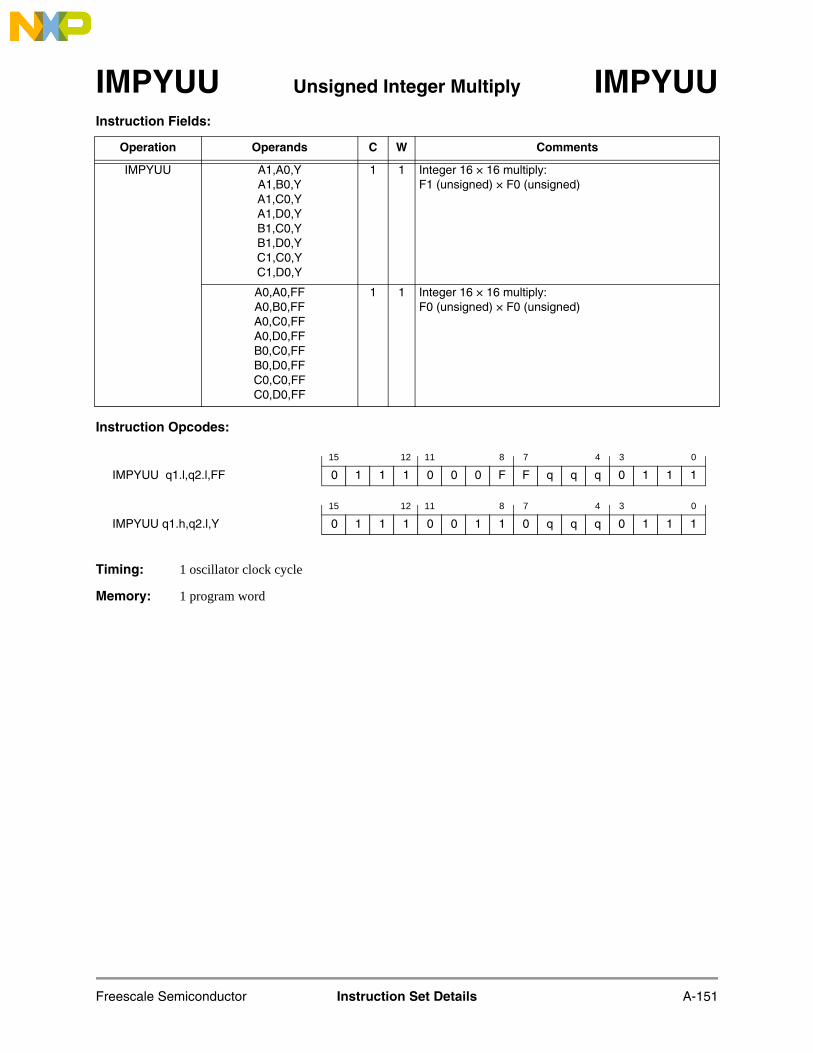
IMPYUU Unsigned Integer Multiply IMPYUUInstruction Fields:
Instruction Opcodes:
Timing: 1 oscillator clock cycle
Memory: 1 program word
Operation Operands C W Comments
IMPYUU A1,A0,YA1,B0,YA1,C0,YA1,D0,YB1,C0,YB1,D0,YC1,C0,YC1,D0,Y
1 1 Integer 16 × 16 multiply:F1 (unsigned) × F0 (unsigned)
A0,A0,FFA0,B0,FFA0,C0,FFA0,D0,FFB0,C0,FFB0,D0,FFC0,C0,FFC0,D0,FF
1 1 Integer 16 × 16 multiply:F0 (unsigned) × F0 (unsigned)
15 12 11 8 7 4 3 0
IMPYUU q1.l,q2.l,FF 0 1 1 1 0 0 0 F F q q q 0 1 1 1
15 12 11 8 7 4 3 0
IMPYUU q1.h,q2.l,Y 0 1 1 1 0 0 1 1 0 q q q 0 1 1 1
Freescale Semiconductor Instruction Set Details A-151

INC.BP Increment Byte (Byte Pointer) INC.BPOperation: Assembler Syntax:
D + 1 → D (no parallel move) INC.BP D (no parallel move)
Description: Increment a byte value in memory. The value is internally sign extended to 20 bits before being incre-mented. The low-order 8 bits of the result are stored back to memory. The condition codes are calcu-lated based on the 8-bit result, with the exception of the E and U bits, which are calculated based onthe 20-bit result. Absolute addresses are expressed as byte addresses. The result is not affected by thestate of the saturation bit (SA).
Usage: This instruction is typically used when integer data is processed.
Example:
INC.BP X:$3065 ; increment the byte at (byte) address $3065
Explanation of Example:Prior to execution, the value at byte address X:$3065 is $00. Execution of the INC.BP instruction in-crements this value by one and generates the result $01. Note that this address is equivalent to the upperbyte of word address $1832.
Condition Codes Affected:
E — Set if the extension portion of the 20-bit result is in useU — Set if the 20-bit result is unnormalizedN — Set if bit 7 of the result is setZ — Set if the result is zeroV — Set if overflow has occurred in resultC — Set if a carry occurs from bit 7 of the result
$3064
$3066
$3068
$3062
X Memory
22 11
7 0
77
00 33
558866
ByteAddresses 70
$3064
$3066
$3068
$3062
X Memory
22 11
7 0
77
01 33
558866
ByteAddresses 70
Before Execution After Execution
0300SR 0310SR
LF P4 P3 P2 P1 P0 I1 I0 SZ L E U N Z V C
MR CCR
15 14 13 12 11 10 9 8 7 6 5 4 3 2 1 0
A-152 DSP56800E and DSP56800EX Core Reference Manual Freescale Semiconductor

INC.BP Increment Byte (Byte Pointer) INC.BPInstruction Fields:
Instruction Opcodes:
Timing: 3–4 oscillator clock cycles
Memory: 2–3 program words
Operation Operands C W Comments
INC.BP X:xxxx 3 2 Increment byte in memory
X:xxxxxx 4 3
15 12 11 8 7 4 3 0
INC.BP X:xxxx 0 1 0 0 1 1 1 0 1 1 0 0 0 1 1 0
AAAAAAAAAAAAAAAA
15 12 11 8 7 4 3 0
INC.BP X:xxxxxx 1 1 1 0 0 A A A 0 A 1 1 A A A A
0 1 0 0 1 1 1 0 1 1 0 0 0 1 1 0
AAAAAAAAAAAAAAAA
Freescale Semiconductor Instruction Set Details A-153

INC.L Increment Long INC.LOperation: Assembler Syntax:
D + 1 → D (no parallel move) INC.L D (no parallel move)
Description: Increment a long-word value in a register or memory. When an operand located in memory is operatedon, the low-order 32 bits of the result are stored back to memory. The condition codes are calculatedbased on the 32-bit result. Absolute addresses pointing to long elements must always be even aligned(that is, pointing to the lowest 16 bits).
Usage: This instruction is typically used when integer data is processed.
Example:
INC.L A ; increment value in A by one
Explanation of Example:Prior to execution, the 36-bit A accumulator contains the value $0:0020:0000. Execution of the INC.Linstruction adds one to the A accumulator. The CCR is updated based on the result of the addition.
Condition Codes Affected:
E — Set if the extension portion of the 36-bit result is in useU — Set if the 36-bit result is unnormalizedN — Set if bit 31 of the result is setZ — Set if the result is zeroV — Set if overflow has occurred in resultC — Set if a carry occurs from bit 31 of the result
Before Execution
000000200
A2 A1 A0
After Execution
000100200
A2 A1 A0
0300SR 0310SR
LF P4 P3 P2 P1 P0 I1 I0 SZ L E U N Z V C
MR CCR
15 14 13 12 11 10 9 8 7 6 5 4 3 2 1 0
A-154 DSP56800E and DSP56800EX Core Reference Manual Freescale Semiconductor

INC.L Increment Long INC.LInstruction Fields:
Instruction Opcodes:
Timing: 1–4 oscillator clock cycle(s)
Memory: 1–3 program word(s)
Operation Operands C W Comments
INC.L fff 1 1 Increment long
X:xxxx 3 2 Increment long in memory
X:xxxxxx 4 3
15 12 11 8 7 4 3 0
INC.L X:xxxx 0 1 0 0 1 1 1 0 1 1 0 0 0 1 1 1
AAAAAAAAAAAAAAAA
15 12 11 8 7 4 3 0
INC.L X:xxxxxx 1 1 1 0 0 A A A 0 A 1 1 A A A A
0 1 0 0 1 1 1 0 1 1 0 0 0 1 1 1
AAAAAAAAAAAAAAAA
15 12 11 8 7 4 3 0
INC.L fff 0 1 1 1 0 0 f f f 0 0 1 0 0 1 1
Freescale Semiconductor Instruction Set Details A-155

INC.W Increment Word INC.WOperation: Assembler Syntax:
D + 1 → D (one parallel move) INC.W D (one parallel move)D + 1 → D (no parallel move) INC.W D (no parallel move)
Description: Increment a 16-bit destination by one. If the destination is an accumulator, only the EXT and MSP por-tions of the accumulator are used and the LSP remain unchanged. The condition codes are calculatedbased on the 16-bit result (or on the 20-bit result for accumulators).
Usage: This instruction is typically used when integer data is processed.
Example:
INC.W A X:(R0)+,X0 ; Increment the 20 MSBs of A and; update X0 and R0
Explanation of Example:Prior to execution, the 36-bit A accumulator contains the value $0:FFFF:0033. Execution of theINC.W instruction increments by one the upper 20 bits of the A accumulator and sets the E and U bitsin the CCR. A new value is read in parallel and stored in register X0; the address register R0 is post-in-cremented.
Condition Codes Affected:
SZ — Set according to the standard definition of the SZ bit (parallel move)L — Set if limiting (parallel move) or overflow has occurred in resultE — Set if the extension portion of the result is in useU — Set if result is unnormalizedN — Set if MSB of the result is setZ — Set if the result is zero (20 MSB for accumulator destinations)V — Set if overflow has occurred in resultC — Set if a carry (or borrow) occurs from bit 15 of the result (bit 35 for accumulators)
Note: When the destination is one of the four accumulators, condition code calculations follow the rules for20-bit arithmetic; otherwise, the rules for 16-bit arithmetic apply.
Before Execution
0033FFFF0
A2 A1 A0
After Execution
003300001
A2 A1 A0
0300SR 0330SR
LF P4 P3 P2 P1 P0 I1 I0 SZ L E U N Z V C
MR CCR
15 14 13 12 11 10 9 8 7 6 5 4 3 2 1 0
A-156 DSP56800E and DSP56800EX Core Reference Manual Freescale Semiconductor

INC.W Increment Word INC.WInstruction Fields:
Parallel Moves:
Operation Operands C W Comments
INC.W EEE 1 1 Increment word.
X:(Rn) 3 1 Increment word in memory using appropriate address-ing mode.X:(Rn+xxxx) 4 2
X:(SP–xx) 4 1
X:xxxx 3 2
X:xxxxxx 4 3
Data ALU Operation Parallel Memory Move
Operation Operands Source Destination1
1.The case where the destination of the data ALU operation is the same register as the destination of the par-allel read operation is not allowed. Memory writes are allowed in this case.
INC.W2
2.This instruction occupies only 1 program word and executes in 1 cycle for every addressing mode.
F X:(Rj)+X:(Rj)+N
X0Y1Y0ABCA1B1
X0Y1Y0ABCA1B1
X:(Rj)+X:(Rj)+N
Freescale Semiconductor Instruction Set Details A-157

INC.W Increment Word INC.WInstruction Opcodes:
Timing: 1–4 oscillator clock cycle(s)
Memory: 1–3 program word(s)
15 12 11 8 7 4 3 0
INC.W EEE 0 1 1 1 0 0 E E E 0 0 0 0 0 1 1
15 12 11 8 7 4 3 0
INC.W F GGG,X:<ea_m> 0 0 0 0 0 G G G F 0 1 1 0 m R R
15 12 11 8 7 4 3 0
INC.W F X:<ea_m>,GGG 0 0 1 0 0 G G G F 0 1 1 0 m R R
15 12 11 8 7 4 3 0
INC.W X:(Rn) 0 1 0 0 1 1 1 0 1 1 0 1 R 1 R R
15 12 11 8 7 4 3 0
INC.W X:(Rn+xxxx) 0 1 0 0 1 1 1 0 1 1 0 1 R 0 R R
AAAAAAAAAAAAAAAA
15 12 11 8 7 4 3 0
INC.W X:(SP–xx) 0 1 0 0 1 0 1 0 1 1 a a a a a a
15 12 11 8 7 4 3 0
INC.W X:xxxx 0 1 0 0 1 1 1 0 1 1 0 0 0 1 0 0
AAAAAAAAAAAAAAAA
15 12 11 8 7 4 3 0
INC.W X:xxxxxx 1 1 1 0 0 A A A 0 A 1 1 A A A A
0 1 0 0 1 1 1 0 1 1 0 0 0 1 0 0
AAAAAAAAAAAAAAAA
A-158 DSP56800E and DSP56800EX Core Reference Manual Freescale Semiconductor

Jcc Jump Conditionally JccOperation: Assembler Syntax:
If (cc), then S → PC Jcc S {<ABS19> or <ABS21>}else PC + 1 → PC
Description: If the specified condition is true, program execution continues at the effective address specified in theinstruction. If the specified condition is false, the PC is incremented and program execution continuessequentially. The effective address is a 19- or 21-bit absolute address.
The term “cc” specifies the following:
Example:
JCS LABEL ; jump to LABEL if carry bit is setINC.W AINC.W A
LABELADD B,A
Explanation of Example:In this example, if C is one when the JCS instruction is executed, program execution skips the twoINC.W instructions and continues with the ADD instruction. If the specified condition is not true, nojump is taken, the program counter is incremented by one, and program execution continues with thefirst INC.W instruction. The Jcc instruction uses a 19-bit absolute address for this example.
Restrictions:Refer to Section 10.4, “Pipeline Dependencies and Interlocks,” on page 10-26.
Condition Codes Affected:The condition codes are tested but not modified by this instruction.
“cc” Mnemonic Condition
CC (HS*)— carry clear (higher or same) C = 0
CS (LO*)— carry set (lower) C = 1
EQ— equal Z = 1
GE— greater than or equal N ⊕ V = 0
GT— greater than Z + (N ⊕ V) = 0
LE— less than or equal Z + (N ⊕ V) = 1
LT— less than N ⊕ V = 1
NE— not equal Z = 0
NN— not normalized Z + (U • E) = 0
NR— normalized Z + (U • E) = 1
* Only available when CM bit is set in the OMR
Xdenotes the logical complement of X+denotes the logical OR operator•denotes the logical AND operator⊕denotes the logical exclusive OR operator
Freescale Semiconductor Instruction Set Details A-159

Jcc Jump Conditionally JccInstruction Fields:
Instruction Opcodes:
Timing: 4–6 oscillator clock cycles
Memory: 2–3 program words
Operation Operands C1
1.The clock-cycle count depends on whether the jump is taken. The first value applies if the jump is taken, andthe second applies if it is not.
W Comments
Jcc <ABS19> 5 or 4 2 19-bit absolute address
<ABS21> 6 or 5 3 21-bit absolute address
15 12 11 8 7 4 3 0
Jcc <ABS21> 1 1 1 0 0 A A A 0 A 1 1 A A A A
1 1 1 0 0 C C C 0 1 0 1 0 C 0 0
AAAAAAAAAAAAAAAA
15 12 11 8 7 4 3 0
Jcc <ABS19> 1 1 1 0 0 C C C 0 1 0 1 A C A A
AAAAAAAAAAAAAAAA
A-160 DSP56800E and DSP56800EX Core Reference Manual Freescale Semiconductor

JMP Unconditional Jump JMPOperation: Assembler Syntax:
S → PC JMP S {(N) or <ABS19> or <ABS21>}
Description: Jump to program memory at the location given by the instruction’s effective address, which can be thevalue in the N register or a 19- or 21- bit absolute address.
Example:
JMP LABEL
Explanation of Example:In this example, program execution is transferred to the address represented by LABEL. The DSC coresupports up to 21-bit program addresses.
Condition Codes Affected:The condition codes are not affected by this instruction.
Restrictions:Refer to Section 10.4, “Pipeline Dependencies and Interlocks,” on page 10-26.
Instruction Fields:
Instruction Opcodes:
Timing: 4–5 oscillator clock cycles
Memory: 1–3 program word(s)
Operation Operands C W Comments
JMP (N) 5 1 Jump to target contained in N register
<ABS19> 4 2 19-bit absolute address
<ABS21> 5 3 21-bit absolute address
15 12 11 8 7 4 3 0
JMP <ABS21> 1 1 1 0 0 A A A 0 A 1 1 A A A A
1 1 1 0 0 0 0 1 0 1 0 1 0 1 0 0
AAAAAAAAAAAAAAAA
15 12 11 8 7 4 3 0
JMP (N) 1 1 1 0 0 1 1 1 0 0 0 1 1 1 1 1
15 12 11 8 7 4 3 0
JMP <ABS19> 1 1 1 0 0 0 0 1 0 1 0 1 A 1 A A
AAAAAAAAAAAAAAAA
Freescale Semiconductor Instruction Set Details A-161

JMPD Delayed Unconditional Jump JMPDOperation: Assembler Syntax:
Execute instructions in next 2 words JMPD S {<ABS19> or <ABS21>}S→ PC
Description: Jump to program memory at the location that is given by the instruction’s effective address, but executethe following 2 words of instructions before completing the jump. That is, execute the next two 1-wordinstructions or the next single 2-word instruction following the JMPD instruction before jumping tothe destination address.
Example:
JMPD LABEL ; delayed JMP to label ADD.W #1,X0 ; first delay slot NOP ; second delay slot (unused)...
LABEL ; JMP target address
Explanation of Example:In this example, program execution is transferred to the address represented by LABEL after the two1-word instructions following the JMPD instruction are executed.
Condition Codes Affected:The condition codes are not affected by this instruction.
Restrictions:Refer to Section 10.4, “Pipeline Dependencies and Interlocks,” on page 10-26.Refer to Section 4.3.2, “Delayed Instruction Restrictions,” on page 4-14.
Instruction Fields:
Instruction Opcodes:
Timing: 2–3 oscillator clock cycles
Memory: 2–3 program words
Operation Operands C W Comments
JMPD <ABS19> 2 2 Delayed jump with 19-bit absolute address; must fill 2 delay slots
<ABS21> 3 3 Delayed jump with 21-bit absolute address; must fill 2 delay slots
15 12 11 8 7 4 3 0
JMPD <ABS21> 1 1 1 0 0 A A A 0 A 1 1 A A A A
1 1 1 0 0 0 1 1 0 1 0 1 0 1 0 0
AAAAAAAAAAAAAAAA
15 12 11 8 7 4 3 0
JMPD <ABS19> 1 1 1 0 0 0 1 1 0 1 0 1 A 1 A A
AAAAAAAAAAAAAAAA
A-162 DSP56800E and DSP56800EX Core Reference Manual Freescale Semiconductor

JSR Jump to Subroutine JSROperation: Assembler Syntax:
SP + 1 → SP JSR S {(RRR) or <ABS19> or <ABS21>}PC → X:(SP)SP + 1 → SPSR → X:(SP)S → PC
Description: Jump to subroutine in program memory located at the effective address specified by the operand. Theoperand can be a 19- or 21-bit absolute address or a register.
Example:
JSR LABEL ; jump to absolute address indicated by “LABEL”
Explanation of Example:In this example, program execution is transferred to the subroutine at the address that is represented byLABEL. The DSC core supports program addresses up to 21 bits wide.
Condition Codes Affected:The condition codes are not affected by this instruction.
Restrictions:Refer to Section 10.4, “Pipeline Dependencies and Interlocks,” on page 10-26.
Instruction Fields:
Instruction Opcodes:
Timing: 4–5 oscillator clock cycles
Memory: 1–3 program word(s)
Operation Operands C W Comments
JSR (RRR) 5 1 Push 21-bit return address and jump to target address contained in the RRR register
<ABS19> 4 2 Push 21-bit return address and jump to 19-bit target address
<ABS21> 5 3 Push 21-bit return address and jump to 21-bit target address
15 12 11 8 7 4 3 0
JSR (RRR) 1 1 1 0 0 1 1 0 0 0 0 1 N 1 N N
15 12 11 8 7 4 3 0
JSR <ABS19> 1 1 1 0 0 0 1 0 0 1 0 1 A 1 A A
AAAAAAAAAAAAAAAA
15 12 11 8 7 4 3 0
JSR <ABS21> 1 1 1 0 0 A A A 0 A 1 1 A A A A
1 1 1 0 0 0 1 0 0 1 0 1 0 1 0 0
AAAAAAAAAAAAAAAA
Freescale Semiconductor Instruction Set Details A-163

LSL.W Logical Shift Left Word LSL.WOperation: Assembler Syntax:
(see following figure) LSL.W D (no parallel move)
Description: Logically shift 16 bits of the destination operand (D) by 1 bit to the left, and store the result in the des-tination. If the destination is a 36-bit accumulator, the result is stored in the MSP of the accumulator(FF1 portion), and the remaining portions of the accumulator are not modified. The MSB of the desti-nation (bit 31 if the destination is a 36-bit accumulator) prior to the execution of the instruction is shift-ed into C, and zero is shifted into the LSB of D1 (bit 16 if the destination is a 36-bit accumulator). Theresult is not affected by the state of the saturation bit (SA).
Example:
LSL.W B ; multiply B1 by 2
Explanation of Example:Prior to execution, the 36-bit B accumulator contains the value $6:C555:00AA. Execution of theLSL.W instruction shifts the 16-bit value in the B1 register by 1 bit to the left and stores the result backin the B1 register. The C bit is set because bit 31 of B1 was set prior to the execution of the instruction.The N bit is also set because bit 31 of accumulator B is set. The overflow bit V is always cleared.
Condition Codes Affected:
N — Set if bit 31 of an accumulator result or bit 15 of a 16-bit register result is setZ — Set if the MSP of result or all bits of a 16-register result are zeroV — Always clearedC — Set if bit 31 of accumulator or bit 15 of a 16-bit register was set prior to the execution
of the instruction
C
D0D2 D1
0UnchangedUnch.
Before Execution
00AAC5556
B2 B1 B0
0302SR
After Execution
00AA8AAA6
B2 B1 B0
0309SR
LF P4 P3 P2 P1 P0 I1 I0 SZ L E U N Z V C
MR CCR
15 14 13 12 11 10 9 8 7 6 5 4 3 2 1 0
A-164 DSP56800E and DSP56800EX Core Reference Manual Freescale Semiconductor

LSL.W Logical Shift Left Word LSL.WInstruction Fields:
Instruction Opcodes:
Timing: 1 oscillator clock cycle
Memory: 1 program word
Operation Operands C W Comments
LSL.W EEE 1 1 1-bit logical shift left word
15 12 11 8 7 4 3 0
LSL.W EEE 0 1 1 1 0 0 E E E 1 1 1 0 0 1 1
Freescale Semiconductor Instruction Set Details A-165

LSR.W Logical Shift Right Word LSR.WOperation: Assembler Syntax:
(see following figure) LSR.W D (no parallel move)
Description: Logically shift 16 bits of the destination operand (D) by 1 bit to the right, and store the result in thedestination. If the destination is a 36-bit accumulator, the result is stored in the MSP of the accumulator(FF1 portion), and the remaining portions of the accumulator are not modified. The LSB of the desti-nation (bit 16 if the destination is a 36-bit accumulator) prior to the execution of the instruction is shift-ed into C, and zero is shifted into the MSB of D1 (bit 31 if the destination is a 36-bit accumulator). Theresult is not affected by the state of the saturation bit (SA).
Example:
LSR.W B ; divide B1 by 2 (B1 considered unsigned)
Explanation of Example:Prior to execution, the 36-bit B accumulator contains the value $F:0001:00AA. Execution of theLSR.W instruction shifts the 16-bit value in the B1 register by 1 bit to the right and stores the resultback in the B1 register. C is set by the operation because bit 0 of B1 was set prior to the execution ofthe instruction. The Z bit of CCR (bit 2) is also set because the result in B1 is zero. The overflow bit(V) is always cleared.
Condition Codes Affected:
N — Always clearedZ — Set if the MSP of result or all bits of a 16-register result are zeroV — Always clearedC — Set if bit 31 of accumulator or bit 15 of a 16-bit register was set prior to the execution
of the instruction
0
D0D2 D1
CUnchangedUnch.
Before Execution
00AA0001F
B2 B1 B0
After Execution
00AA0000F
B2 B1 B0
0302SR 0305SR
LF P4 P3 P2 P1 P0 I1 I0 SZ L E U N Z V C
MR CCR
15 14 13 12 11 10 9 8 7 6 5 4 3 2 1 0
A-166 DSP56800E and DSP56800EX Core Reference Manual Freescale Semiconductor

LSR.W Logical Shift Right Word LSR.WInstruction Fields:
Instruction Opcodes:
Timing: 1 oscillator clock cycle
Memory: 1 program word
Operation Operands C W Comments
LSR.W EEE 1 1 1-bit logical shift right word
15 12 11 8 7 4 3 0
LSR.W EEE 0 1 1 1 0 0 E E E 1 1 1 1 0 1 1
Freescale Semiconductor Instruction Set Details A-167

LSR16 Logical Shift Right 16 Bits LSR16Operation: Assembler Syntax:
S >> 16 → D (no parallel move) LSR16 S,D (no parallel move)
Description: Logically shift the source operand to the right by 16 bits, and store the result in the destination (D),zero extending to the left. This operation effectively places the MSP of the source register into the LSPof the destination register, propagating zero bits through the MSP and the extension register (for accu-mulator destinations). If the source is an accumulator, both the extension register and MSP are shifted.When the destination operand is a 16-bit register, the MSP of an accumulator or Y register is writtento it. If both the source and destination are 16-bit registers, the destination is cleared. The result is notaffected by the state of the saturation bit (SA).
Usage: This instruction can be used to cast an unsigned integer to a long value.
Example:
LSR16 Y,A; ; shift MSP of Y into A0
Explanation of Example:Prior to execution, the Y register contains the value to be shifted ($A1A2:A3A4). The contents of thedestination register are not important prior to execution because they have no effect on the calculatedvalue. The LSR16 instruction logically shifts the value $A1A2:A3A4 by 16 bits to the right, zero ex-tends to a full 36 bits, and places the result in the destination register A.
Condition Codes Affected:The condition codes are not affected by this instruction.
Instruction Fields:
Instruction Opcodes:
Timing: 1 oscillator clock cycle
Memory: 1 program word
Operation Operands C W Comments
LSR16 FFF,FFF 1 1 Logical shift right the first operand by 16 bits, placing result in the destination operand (new bits zeroed)
FFF 1 1 An alternate syntax for the preceding instruction if the source and the destination are the same
Before Execution
345634560
A2 A1 A0
After Execution
A1A200000
A2 A1 A0
A3A4A1A2
Y1 Y0
A3A4A1A2
Y1 Y0
15 12 11 8 7 4 3 0
LSR16 FFF,FFF 0 1 1 1 1 1 F F F b b b 0 1 1 1
A-168 DSP56800E and DSP56800EX Core Reference Manual Freescale Semiconductor

LSRA Logical Shift Right AGU Register LSRAOperation: Assembler Syntax:
D >> 1 → D (no parallel move) LSRA D (no parallel move)
Description: Logically shift the address register operand 1 bit to the right, and store the result back in the register.
Example:
LSRA R0 ; logically shift R0 to the right 1 bit
Explanation of Example:Prior to execution, the R0 register contains $A0A0A0. Execution of the LSRA R0 instruction shiftsthe value in the R0 register 1 bit to the right, and stores the result ($505050) back in R0.
Condition Codes Affected:The condition codes are not affected by this instruction.
Instruction Fields:
Instruction Opcodes:
Timing: 1 oscillator clock cycle
Memory: 1 program word
Operation Operands C W Comments
LSRA Rn 1 1 Logical shift right AGU register by 1 bit
Before Execution After Execution
A0A0A0R0 505050R0
15 12 11 8 7 4 3 0
LSRA Rn 1 0 0 0 0 1 0 1 0 0 1 1 R 1 R R
Freescale Semiconductor Instruction Set Details A-169

LSRAC Logical Shift Right with Accumulate LSRACOperation: Assembler Syntax:
(S1 >> S2) + D →D (no parallel move) LSRAC S1,S2,D (no parallel move)
Description: Logically shift the first 16-bit source operand (S1) to the right by the value contained in the lowest4 bits of the second source operand (S2), and accumulate the result with the value in the destination(D). Operand S1 is internally zero extended and concatenated with 16 zero bits to form a 36-bit valuebefore the shift operation. The result is not affected by the state of the saturation bit (SA).
Usage: This instruction is used for multi-precision logical right shifts.
Example:
LSRAC Y1,X0,A ; logical right shift Y1 by 4 and; accumulate in A
Explanation of Example:Prior to execution, the Y1 register contains the value to be shifted ($C003), the lowest 4 bits of the X0register contain the amount by which to shift ($4), and the destination accumulator contains$0:0000:0099. The LSRAC instruction logically shifts the value $C003 by 4 bits to the right and ac-cumulates this result with the value that is already in accumulator A.
Condition Codes Affected:
N — Set if bit 35 of accumulator result is setZ — Set if accumulator result equals zero
Note: If the SA bit is set, the N bit is equal to bit 31 of the result; if SA is cleared, N is equal to bit 35 of theresult.
Before Execution
009900000
A2 A1 A0
00F4X0
After Execution
30990C000
A2 A1 A0
00F4X0
0300SR 0300SR
8000C003
Y1 Y0
8000C003
Y1 Y0
LF P4 P3 P2 P1 P0 I1 I0 SZ L E U N Z V C
MR CCR
15 14 13 12 11 10 9 8 7 6 5 4 3 2 1 0
A-170 DSP56800E and DSP56800EX Core Reference Manual Freescale Semiconductor

LSRAC Logical Shift Right with Accumulate LSRACInstruction Fields:
Instruction Opcodes:
Timing: 1 oscillator clock cycle
Memory: 1 program word
Operation Operands C W Comments
LSRAC Y1,X0,FFY0,X0,FFY1,Y0,FFY0,Y0,FFA1,Y0,FFB1,Y1,FFC1,Y0,FFC1,Y1,FF
1 1 Logical word shift right with accumulation
15 12 11 8 7 4 3 0
LSRAC Q1,Q2,FF 0 1 1 1 0 1 0 F F Q Q Q 0 1 1 0
Freescale Semiconductor Instruction Set Details A-171

LSRR.L Multi-Bit Logical Right Shift Long LSRR.LOperation: Assembler Syntax:
If S[15] = 0 or S is not a register,D >> S → D (no parallel move) LSRR.L S,D (no parallel move)ElseD << –S → D (no parallel move) LSRR.L S,D (no parallel move)
Description: Logically shift the second operand to the right by the value contained in the 5 lowest bits of the firstoperand (or by an immediate integer), and store the result back in the destination (D). The shift countcan be a 5-bit positive immediate integer or the value contained in X0, Y0, Y1, or the MSP of an ac-cumulator. For 36- and 32-bit destinations, the MSP:LSP are shifted, with zero extension from bit 31(the FF2 portion is ignored). If the shift count in a register is negative (bit 15 is set), the direction ofthe shift is reversed. The result is not affected by the state of the saturation bit (SA).
Example:
LSRR.L Y1,A ; left shift 32-bit A10 by Y1
Explanation of Example:Prior to execution, the A accumulator contains the value to be shifted, $F:F123:3456, and the Y1 reg-ister contains the amount by which to shift ($10 = 16). The LSRR.L instruction logically shifts the des-tination accumulator 16 bits to the right and places the result back in A.
Condition Codes Affected:
N — Set if the MSB of the result is setZ — Set if the result equals zero
Note: Condition code results are set according to the size of the destination operand.
Before Execution
3456F123F
A2 A1 A0
After Execution
F12300000
A2 A1 A0
0300SR 0300SR
80000010
Y1 Y0
80000010
Y1 Y0
LF P4 P3 P2 P1 P0 I1 I0 SZ L E U N Z V C
MR CCR
15 14 13 12 11 10 9 8 7 6 5 4 3 2 1 0
A-172 DSP56800E and DSP56800EX Core Reference Manual Freescale Semiconductor

LSRR.L Multi-Bit Logical Right Shift Long LSRR.LInstruction Fields:
Instruction Opcodes:
Timing: 2 oscillator clock cycles
Memory: 1 program word
Operation Operands C W Comments
LSRR.L #<0–31>,fff 2 1 Logical shift right by a 5-bit positive immediate integer
EEE,FFF 2 1 Bi-directional logical shift destination by value in the first operand: positive –> right shift
15 12 11 8 7 4 3 0
LSRR.L #<0–31>,fff 0 1 0 0 1 1 f f f 0 1 B B B B B
15 12 11 8 7 4 3 0
LSRR.L EEE,FFF 0 1 1 1 1 1 F F F a a a 1 1 0 1
Freescale Semiconductor Instruction Set Details A-173

LSRR.W Multi-Bit Logical Right Shift Word LSRR.WOperation: Assembler Syntax:
D >> S → D (no parallel move) LSRR.W S,D (no parallel move)S1 >> S2 → D (no parallel move) LSRR.W S1,S2,D (no parallel move)
Description: This instruction can have two or three operands. Logically shift the source operand S1 or D to the rightby the value contained in the lowest 4 bits of either S2 or S, respectively (or by an immediate integer),and store the result in the destination (D). The shift count can be a 4-bit positive integer, a value in a16-bit register, or the MSP of an accumulator. For 36- and 32-bit destinations, only the MSP is shiftedand the LSP is cleared, with zero extension from bit 31 (the FF2 portion is ignored). The result is notaffected by the state of the saturation bit (SA).
Example 1:LSRR.W Y1,Y0,A ; logical right shift of 16-bit Y1 by
; least 4 bits of Y0
Explanation of Example:Prior to execution, the Y1 register contains the value to be shifted ($AAAA), and the Y0 register con-tains the amount by which to shift (least 4 bits of $FFF1 = 1). The contents of the destination registerare not important prior to execution because they have no effect on the calculated value. The LSRR.Winstruction logically shifts the value $AAAA by 1 bit to the right and places the result in the destinationregister A (the LSP is cleared).
Example 2:LSRR.W Y1,A ; logical right shift of 16-bit A1 by
; least 4 bits of Y1
Explanation of Example:Prior to execution, A1 contains the value that is to be shifted ($AAAA), and the Y1 register containsthe amount by which to shift ($1). The LSRR.W instruction logically shifts the zero-extended value$AAAA by 1 bit to the right and places the result in the destination register A (the LSP is cleared).
Before Execution
345634560
A2 A1 A0
After Execution
000055550
A2 A1 A0
0300SR 0300SR
FFF1AAAA
Y1 Y0
FFF1AAAA
Y1 Y0
Before Execution
4567AAAAF
A2 A1 A0
After Execution
000055550
A2 A1 A0
0300SR 0300SR
000F0001
Y1 Y0
000F0001
Y1 Y0
A-174 DSP56800E and DSP56800EX Core Reference Manual Freescale Semiconductor

LSRR.W Multi-Bit Logical Right Shift Word LSRR.WCondition Codes Affected:
N — Set if MSB of result is setZ — Set if accumulator result equals zero
Instruction Fields:
Instruction Opcodes:
Timing: 1 oscillator clock cycle
Memory: 1 program word
Operation Operands C W Comments
LSRR.W #<0–15>,FFF 1 1 Logical shift right by a 4-bit positive immediate integer(sign extends into FF2)
EEE,FFF 1 1 Logical shift right destination by value specified in 4 LSBs of the first operand (sign extends into FF2)
Y1,X0,FFFY0,X0,FFFY1,Y0,FFFY0,Y0,FFFA1,Y0,FFFB1,Y1,FFFC1,Y0,FFFC1,Y1,FFF
1 1 Logical shift right the first operand by value specified in 4 LSBs of the second operand; places result in FFF, sign extends into FF2
LF P4 P3 P2 P1 P0 I1 I0 SZ L E U N Z V C
MR CCR
15 14 13 12 11 10 9 8 7 6 5 4 3 2 1 0
15 12 11 8 7 4 3 0
LSRR.W #<0–15>,FFF 0 1 0 1 1 1 F F F 0 1 0 B B B B
15 12 11 8 7 4 3 0
LSRR.W EEE,FFF 0 1 1 1 1 1 F F F a a a 1 0 0 1
15 12 11 8 7 4 3 0
LSRR.W Q1,Q2,FFF 0 1 1 1 0 1 F F F Q Q Q 0 0 1 0
Freescale Semiconductor Instruction Set Details A-175

MAC Multiply-Accumulate MACOperation: Assembler Syntax:
D + (S1 × S2) → D (no parallel move) MAC (+)S1,S2,D (no parallel move)D + (S1 × S2) → D (one parallel move) MAC (+)S1,S2,D (one parallel move)D + (S1 × S2) → D (two parallel reads) MAC S1,S2,D (two parallel reads)
Description: Multiply the two signed 16-bit source operands, and add or subtract the 32-bit fractional product to orfrom the destination (D). Both source operands must be located in the FF1 portion of an accumulatoror in X0, Y0, or Y1. The fractional product is first sign extended before the 36-bit addition (or subtrac-tion) is performed. If the destination is one of the 16-bit registers, it is first sign extended internally andconcatenated with 16 zero bits to form a 36-bit operand before the operation to the fractional product;the high-order 16 bits of the result are then stored.
Usage: This instruction is used for the multiplication and accumulation of fractional data or integer data whena full 32-bit product is required (see Section 5.3.3, “Multiplication,” on page 5-18). When the destina-tion is a 16-bit register, this instruction is useful only for fractional data.
Example:
MAC Y0,X0,A X:(R0)+,Y0 X:(R3)+,X0 ; fractional MAC, two reads
Explanation of Example:Prior to execution, the 16-bit X0 register contains the value $0280 (or fractional value 0.019531250),the 16-bit Y0 register contains the value $0200 (or fractional value 0.015625), and the 36-bit A accu-mulator contains the value $0:0000:8000 (or fractional value 0.000015259). Execution of the MACinstruction multiplies the 16-bit signed value in the X0 register by the 16-bit signed value in Y0 (yield-ing the fractional product result of $000A:0000 = 0.000305176), adds the resulting 32-bit product tothe 36-bit A accumulator, and stores the result ($0:000A:8000 = 0.00320435) back into the A accumu-lator. In parallel, X0 and Y0 are updated with new values that are fetched from the data memory, andthe two address registers (R0 and R3) are post-incremented by one.
Condition Codes Affected:
SZ — Set according to the standard definition of the SZ bit (parallel move)L — Set if limiting (parallel move) or overflow has occurred in resultE — Set if the extension portion of accumulator result is in useU — Set according to the standard definition of the U bitN — Set if MSB of result is setZ — Set if accumulator result equals zeroV — Set if overflow has occurred in accumulator result
Before Execution
800000000
A2 A1 A0
0280X0
After Execution
8000000A0
A2 A1 A0
0288X0
0300SR 0310SR
0200FF00
Y1 Y0
0300FF00
Y1 Y0
LF P4 P3 P2 P1 P0 I1 I0 SZ L E U N Z V C
MR CCR
15 14 13 12 11 10 9 8 7 6 5 4 3 2 1 0
A-176 DSP56800E and DSP56800EX Core Reference Manual Freescale Semiconductor

MAC Multiply-Accumulate MACInstruction Fields:
Parallel Moves:
Parallel Dual Reads:
Operation Operands C W Comments
MAC (±)FFF1,FFF1,FFF 1 1 Fractional multiply-accumulate; multiplication result optionally negated before accumulation.
Data ALU Operation Parallel Memory Move
Operation Operands Source Destination1
1.The case where the destination of the data ALU operation is the same register as the destination of the par-allel read operation is not allowed. Memory writes are allowed in this case.
MAC2
2.This instruction occupies only 1 program word and executes in 1 cycle for every addressing mode.
Y1,X0,FY0,X0,FY1,Y0,FY0,Y0,F
A1,Y0,FB1,Y1,FC1,Y0,FC1,Y1,F
–C1,Y0,F–C1,Y1,F
X:(Rj)+X:(Rj)+N
X0Y1Y0ABCA1B1
X0Y1Y0ABCA1B1
X:(Rj)+X:(Rj)+N
Data ALU Operation1
1.This instruction is not allowed when the XP bit in the OMR is set (that is, when the instructions are executingfrom data memory).
First Memory Read Second Memory Read
Operation Operands Source 1 Destination 1 Source 2 Destination 2
MAC2
2.This instruction occupies only 1 program word and executes in 1 cycle for every addressing mode.
Y1,X0,FY1,Y0,FY0,X0,FC1,Y0,F
X:(R0)+X:(R0)+NX:(R1)+
X:(R1)+N
Y0Y1
X:(R3)+X:(R3)–
X0
X:(R4)+X:(R4)+N
Y0 X:(R3)+X:(R3)+N3
X0
X:(R0)+X:(R0)+NX:(R4)+
X:(R4)+N
Y1 X:(R3)+X:(R3)+N3
C
Freescale Semiconductor Instruction Set Details A-177

MAC Multiply-Accumulate MACInstruction Opcodes:
Timing: 1 oscillator clock cycle
Memory: 1 program word
15 12 11 8 7 4 3 0
MAC –C1,Q2,F GGG,X:<ea_m> 0 0 0 1 0 G G G F Q Q Q 1 m R R
15 12 11 8 7 4 3 0
MAC –C1,Q2,F X:<ea_m>,GGG 0 0 1 1 0 G G G F Q Q Q 1 m R R
15 12 11 8 7 4 3 0
MAC FFF1,FFF1,FFF 0 1 1 0 1 0 F F F J J J J J 0 0
15 12 11 8 7 4 3 0
MAC Q1,Q2,F GGG,X:<ea_m> 0 0 0 0 1 G G G F Q Q Q 1 m R R
15 12 11 8 7 4 3 0
MAC Q1,Q2,F X:<ea_m>,GGG 0 0 1 0 1 G G G F Q Q Q 1 m R R
15 12 11 8 7 4 3 0
MAC Q3,Q4,F X:<ea_m>,reg1 X:<ea_v>,reg2
0 1 1 0 0 1 v v F v Q Q 1 m 0 v
15 12 11 8 7 4 3 0
MAC –FFF1,FFF1,FFF 0 1 1 0 1 1 F F F J J J J J 1 0
A-178 DSP56800E and DSP56800EX Core Reference Manual Freescale Semiconductor

MACR Multiply-Accumulate and Round MACROperation: Assembler Syntax:
D + (S1 × S2) + r → D (no parallel move) MACR (+)S1,S2,D (no parallel move)D + (S1 × S2) + r → D (one parallel move) MACR S1,S2,D (one parallel move)D + (S1 × S2) + r → D (two parallel reads) MACR S1,S2,D (two parallel reads)
Description: Multiply the two signed 16-bit source operands, add or subtract the 32-bit fractional product to or fromthe third operand, and round and store the result in the destination (D). Both source operands must belocated in the FF1 portion of an accumulator or in X0, Y0, or Y1. The fractional product is first signextended before the 36-bit addition is performed, followed by the rounding operation. If the destinationis one of the 16-bit registers, it is first sign extended internally and concatenated with 16 zero bits toform a 36-bit operand before being added to the fractional product. The addition is then followed bythe rounding operation, and the high-order 16 bits of the result are then stored. This instruction usesthe rounding technique that is selected by the R bit in the OMR. When the R bit is cleared (defaultmode), convergent rounding is selected; when the R bit is set, two’s-complement rounding is selected.Refer to Section 5.9, “Rounding,” on page 5-43 for more information about the rounding modes. Notethat the rounding operation always zeros the LSP of the result if the destination (D) is an accumulatoror the Y register.
Usage: This instruction is used for the multiplication, accumulation, and rounding of fractional data.
Example:
MACR Y0,X0,A X:(R0)+,Y0 X:(R3)+,X0 ; multiply-accumulate; fractional with rounding
Explanation of Example:Prior to execution, the 16-bit X0 register contains the value $0280 (or fractional value 0.019531250),the 16-bit Y0 register contains the value $0200 (or fractional value 0.015625), and the 36-bit A accu-mulator contains the value $0:0000:8000 (or fractional value 0.000015259). Execution of the MACRinstruction multiplies the 16-bit signed value in the X0 register by the 16-bit signed value in Y0 (yield-ing the fractional product result of $000A:0000 = 0.000305176), adds the resulting 32-bit product tothe 36-bit A accumulator ($0:000A:8000 = 0.00320435), rounds the result, and stores the rounded re-sult ($0:000A:0000 = 0.000305176) back into the A accumulator. In parallel, X0 and Y0 are updatedwith new values that are fetched from the data memory, and the two address registers (R0 and R3) arepost-incremented by one. In this example, the default rounding technique (convergent rounding) is per-formed (bit R in the OMR is cleared). If two’s-complement rounding is utilized (R bit is set), the resultin accumulator A is $0:000B:0000 = 0.000335693.
Before Execution
800000000
A2 A1 A0
0280X0
After Execution
0000000A0
A2 A1 A0
0288X0
0300SR 0310SR
0200FF00
Y1 Y0
0300FF00
Y1 Y0
Freescale Semiconductor Instruction Set Details A-179

MACR Multiply-Accumulate and Round MACRCondition Codes Affected:
SZ — Set according to the standard definition of the SZ bit (parallel move)L — Set if limiting (parallel move) or overflow has occurred in resultE — Set if the extended portion of accumulator result is in useU — Set according to the standard definition of the U bitN — Set if MSB of result is setZ — Set if result equals zeroV — Set if overflow has occurred in result
Instruction Fields:
Parallel Moves:
Operation Operands C W Comments
MACR (±)FFF1,FFF1,FFF 1 1 Fractional MAC with round; multiplication result optionally negated before addition.
Data ALU Operation Parallel Memory Move
Operation Operands Source Destination1
1.The case where the destination of the data ALU operation is the same register as the destination of the par-allel read operation is not allowed. Memory writes are allowed in this case.
MACR2
2.This instruction occupies only 1 program word and executes in 1 cycle for every addressing mode.
Y1,X0,FY0,X0,FY1,Y0,FY0,Y0,F
A1,Y0,FB1,Y1,FC1,Y0,FC1,Y1,F
X:(Rj)+X:(Rj)+N
X0Y1Y0ABCA1B1
X0Y1Y0ABCA1B1
X:(Rj)+X:(Rj)+N
LF P4 P3 P2 P1 P0 I1 I0 SZ L E U N Z V C
MR CCR
15 14 13 12 11 10 9 8 7 6 5 4 3 2 1 0
A-180 DSP56800E and DSP56800EX Core Reference Manual Freescale Semiconductor

MACR Multiply-Accumulate and Round MACRParallel Dual Reads:
Instruction Opcodes:
Timing: 1 oscillator clock cycle
Memory: 1 program word
Data ALU Operation1
1.This instruction is not allowed when the XP bit in the OMR is set (that is, when the instructions are executingfrom data memory).
First Memory Read Second Memory Read
Operation Operands Source 1 Destination 1 Source 2 Destination 2
MACR2
2.This instruction occupies only 1 program word and executes in 1 cycle for every addressing mode.
Y1,X0,FY1,Y0,FY0,X0,FC1,Y0,F
X:(R0)+X:(R0)+NX:(R1)+
X:(R1)+N
Y0Y1
X:(R3)+X:(R3)–
X0
X:(R4)+X:(R4)+N
Y0 X:(R3)+X:(R3)+N3
X0
X:(R0)+X:(R0)+NX:(R4)+
X:(R4)+N
Y1 X:(R3)+X:(R3)+N3
C
15 12 11 8 7 4 3 0
MACR FFF1,FFF1,FFF 0 1 1 0 1 0 F F F J J J J J 1 0
15 12 11 8 7 4 3 0
MACR Q1,Q2,F GGG,X:<ea_m> 0 0 0 1 1 G G G F Q Q Q 1 m R R
15 12 11 8 7 4 3 0
MACR Q1,Q2,F X:<ea_m>,GGG 0 0 1 1 1 G G G F Q Q Q 1 m R R
15 12 11 8 7 4 3 0
MACR Q3,Q4,F X:<ea_m>,reg1X:<ea_v>,reg2
0 1 1 1 0 1 v v F v Q Q 1 m 0 v
15 12 11 8 7 4 3 0
MACR –FFF1,FFF1,FFF 0 1 1 0 1 1 F F F J J J J J 1 1
Freescale Semiconductor Instruction Set Details A-181

MACSU Multiply-Accumulate Signed × Unsigned MACSUOperation: Assembler Syntax:
D + (S1 × S2) → D (S1 signed, S2 unsigned) MACSU S1,S2,D (no parallel move)
Description: Multiply one signed 16-bit source operand by one unsigned 16-bit operand, and add the 32-bit frac-tional product to the destination (D). The order of the registers is important. The first source register(S1) must contain the signed value, and the second source (S2) must contain the unsigned value to pro-duce correct fractional results. The fractional product is first sign extended before the 36-bit additionis performed. If the destination is one of the 16-bit registers, only the high-order 16 bits of the fractionalresult are stored. The result is not affected by the state of the saturation bit (SA). Note that for 16-bitdestinations, the sign bit may be lost for large fractional magnitudes.
Usage: In addition to single-precision multiplication of a signed-times-unsigned value and accumulation, thisinstruction is used for multi-precision multiplications, as shown in Section 5.5, “Extended- andMulti-Precision Operations,” on page 5-29.
Example:
MACSU Y1,B1,A ; multiply signed Y1 to unsigned B1 and; accumulate in A
Explanation of Example:Prior to execution, the 16-bit Y1 register contains the (signed) negative value $FFF4, and the 16-bitB1 register contains the (unsigned) positive value $0002. Execution of the MACSU instruction multi-plies the 16-bit signed value in the Y1 register by the 16-bit unsigned value in B1 (yielding the frac-tional product result of $FFFF:FFD0), then adds the sign extended result to the A accumulator, andstores the signed result ($F:FFFF:FFF0) back into the A accumulator.
Condition Codes Affected:
L — Set if overflow has occurred in resultE — Set if the extended portion of the result is in useU — Set according to the standard definition of the U bitN — Set if MSB of result is setZ — Set if result equals zeroV — Set if overflow has occurred in result
Before Execution
002000000
A2 A1 A0
0300SR
After Execution
FFF0FFFFF
A2 A1 A0
0318SR
345600020
B2 B1 B0
345600020
B2 B1 B0
8000FFF4
Y1 Y0
8000FFF4
Y1 Y0
LF P4 P3 P2 P1 P0 I1 I0 SZ L E U N Z V C
MR CCR
15 14 13 12 11 10 9 8 7 6 5 4 3 2 1 0
A-182 DSP56800E and DSP56800EX Core Reference Manual Freescale Semiconductor

MACSU Multiply-Accumulate Signed × Unsigned MACSUInstruction Fields:
Instruction Opcodes:
Timing: 1 oscillator clock cycle
Memory: 1 program word
Operation Operands C W Comments
MACSU X0,Y1,EEEX0,Y0,EEEY0,Y1,EEEY0,Y0,EEEY0,A1,EEEY1,B1,EEEY0,C1,EEEY1,C1,EEE
1 1 16 × 16 => 32-bit unsigned/signed fractional MAC.
The first operand is treated as signed and the second as unsigned.
15 12 11 8 7 4 3 0
MACSU Q2,Q1,EEE 0 1 1 1 0 1 E E E Q Q Q 1 1 1 0
Freescale Semiconductor Instruction Set Details A-183

MOVE.B Move Byte (Word Pointer) MOVE.BOperation: Assembler Syntax:
S → D (no parallel move) MOVE.B S,D (no parallel move)
Description: Move an 8-bit value from a register to memory or from memory to a register. Register-indirect memorylocations are specified with word pointers, offsets are specified as byte offsets, and absolute addressesare specified as byte addresses. Register operands are affected as follows:
– If the source operand is a 16-bit register, the lower 8 bits are moved.– If the destination operand is a 16-bit register, the lower 8 bits are written and the upper 8 bits are
filled with sign extension.– If the source operand is an accumulator, the lower 8 bits of FF1 are moved.– If the destination operand is an accumulator, the lower 8 bits of FF1 are written, FF2 and the upper
8 bits of FF1 are filled with sign extension, and FF0 is zero filled.– If the destination operand is the Y register, the lower 8 bits of Y1 are written, the upper 8 bits of Y1
are filled with sign extension, and Y0 is zero filled.Example 1:
MOVE.B X:(R0+$21),A ; move byte from memory into A
Explanation of Example:Prior to the memory move, the accumulator register A contains the value $0:6677:8899. After execu-tion of the MOVE.B X:(R0+$21),A instruction, the FF1 portion of A is updated with the value inmemory that is pointed to by the word pointer R0, with a byte offset of $21, which results in the upperbyte of the word memory X:$4454. The results is sign extended through bit 35 of A. The FF0 portionof A is filled with zero. The content of the A accumulator becomes $F:FF90:0000.
Example 2:MOVE.B X:(R0+$20),X:$2223 ; move byte from memory into memory
Explanation of Example:Prior to execution, the word location X:$1111 contains the value $3333. After execution of theMOVE.B X:(R0+$20),X:$2223 instruction, the lower byte of the word memory location pointedto by (R0+$20), which is location X:$4454, is written to the upper byte of the word memory locationX:$1111, which is specified as X:$2223 in byte address. The value at X:$1111 becomes $6033.
Before Execution After Execution
004444R0 004444R0
X:$4454 9060 X:$4454 9060
889966770
A2 A1 A0
0000FF90F
A2 A1 A0
Before Execution After Execution
X:$1111 3333 X:$1111 6033
004444R0 004444R0
X:$4454 9060 X:$4454 9060
A-184 DSP56800E and DSP56800EX Core Reference Manual Freescale Semiconductor

MOVE.B Move Byte (Word Pointer) MOVE.BCondition Codes Affected:
The condition codes are not affected by this instruction.
Instruction Fields:
Instruction Opcodes:
Operation Source Destination C W Comments
MOVE.B X:(Rn+xxxx) HHH 2 2 Signed 16-bit offset
X:(Rn+xxxxxx) HHH 3 3 24-bit offset
X:(SP) HHH 1 1 Pointer is SP
HHH X:(RRR+x) 2 1 x: offset ranging from 0 to 7
HHH X:(Rn+xxxx) 2 2 Signed 16-bit offset
HHH X:(Rn+xxxxxx) 3 3 24-bit offset
HHH X:(SP–x) 2 1 x: offset ranging from 1 to 8
HHH X:(SP) 1 1 Pointer is SP
X:(Rn+xxxx) X:xxxx 3 3 Signed 16-bit offset
Notes: • Each absolute address operand is specified as a byte address. In this address, all bits except the LSB select the appropriate word location in memory, and the LSB selects the upper or lower byte of that word.
• Pointer Rn is a word pointer.• Offsets x, xxxx, and xxxxxx are byte offsets.
15 12 11 8 7 4 3 0
MOVE.B HHH,X:(RRR+x) 1 0 0 1 1 h h h 0 0 i i N i N N
15 12 11 8 7 4 3 0
MOVE.B HHH,X:(SP–x) 1 0 0 1 1 h h h 0 0 i i 1 i 1 1
15 12 11 8 7 4 3 0
MOVE.B HHH,X:(Rn+xxxx) 1 1 0 1 0 h h h 1 1 1 0 R 0 R R
AAAAAAAAAAAAAAAA
15 12 11 8 7 4 3 0
MOVE.B HHH,X:(Rn+xxxxxx) 1 1 1 0 0 A A A 0 A 1 1 A A A A
1 1 0 1 0 h h h 1 1 1 0 R 0 R R
AAAAAAAAAAAAAAAA
15 12 11 8 7 4 3 0
MOVE.B HHH,X:(SP) 1 1 0 1 0 h h h 1 0 1 1 1 1 1 1
15 12 11 8 7 4 3 0
MOVE.B X:(Rn+xxxx),HHH 1 1 1 1 0 h h h 1 1 1 0 R 0 R R
AAAAAAAAAAAAAAAA
Freescale Semiconductor Instruction Set Details A-185

MOVE.B Move Byte (Word Pointer) MOVE.BInstruction Opcodes:(continued)
Timing: 1–3 oscillator clock cycle(s)
Memory: 1–3 program word(s)
15 12 11 8 7 4 3 0
MOVE.B X:(Rn+xxxx),X:xxxx 1 1 1 1 0 1 1 0 1 1 1 0 R 0 R R
AAAAAAAAAAAAAAAA.s
AAAAAAAAAAAAAAAA.d
15 12 11 8 7 4 3 0
MOVE.B X:(Rn+xxxx),Y 1 1 0 1 0 1 1 0 1 1 1 0 R 0 R R
AAAAAAAAAAAAAAAA
15 12 11 8 7 4 3 0
MOVE.B X:(Rn+xxxxxx),HHH 1 1 1 0 0 A A A 0 A 1 1 A A A A
1 1 1 1 0 h h h 1 1 1 0 R 0 R R
AAAAAAAAAAAAAAAA
15 12 11 8 7 4 3 0
MOVE.B X:(Rn+xxxxxx),Y 1 1 1 0 0 A A A 0 A 1 1 A A A A
1 1 0 1 0 1 1 0 1 1 1 0 R 0 R R
AAAAAAAAAAAAAAAA
15 12 11 8 7 4 3 0
MOVE.B X:(SP),HHH 1 1 1 1 0 h h h 1 0 1 1 1 1 1 1
15 12 11 8 7 4 3 0
MOVE.B X:(SP),Y 1 1 0 1 0 1 1 0 1 0 1 1 1 1 1 1
A-186 DSP56800E and DSP56800EX Core Reference Manual Freescale Semiconductor

MOVE.BP Move Byte (Byte Pointer) MOVE.BPOperation: Assembler Syntax:
S → D (no parallel move) MOVE.BP S,D (no parallel move)
Description: Move an 8-bit value from a register to memory, from memory to a register, or between two memorylocations. Register-indirect memory locations are specified with byte pointers, offsets are specified asbyte offsets, and absolute addresses are specified as byte addresses. Register operands are affected asfollows:
– If the source operand is a 16-bit register, the lower 8 bits are moved.– If the destination operand is a 16-bit register, the lower 8 bits are written and the upper 8 bits are
filled with sign extension.– If the source operand is an accumulator, the lower 8 bits of FF1 are moved.– If the destination operand is an accumulator, the lower 8 bits of FF1 are written, FF2 and the upper
8 bits of FF1 are filled with sign extension, and FF0 is zero filled.– If the destination operand is the Y register, the lower 8 bits of Y1 are written, the upper 8 bits of Y1
are filled with sign extension, and Y0 is zero filled.Example 1:
MOVE.BP X:(R0)+,A; move byte into A, update R0
Explanation of Example:Prior to the memory move, the accumulator register A contains the value $0:6677:8888. After execu-tion of the MOVE.BP X:(R0)+,A instruction, the lower 8 bits of A1 are updated with the value inmemory pointed to by the byte pointer R0, the result is sign extended through bit 35 of A, and the FF0portion is filled with zero. The value in A becomes $F:FF96:0000. The R0 pointer is then incrementedby one.
Example 2:MOVE.BP X0,X:(R0+$21) ; move byte into data memory location
Explanation of Example:Prior to the memory move, the word memory location X:$2232 contains the value $9060. After exe-cution of the MOVE.BP X0,X:(R0+$21) instruction, the lower 8 bits of X0 are written to the upperbyte of the word memory location X:$2232. This memory location is the result of the effective address(R0+$21) in bytes.
Before Execution After Execution
X:$2222 6996 X:$2222 6996
888866770
A2 A1 A0
0000FF96F
A2 A1 A0
004444R0 004445R0
Before Execution After Execution
X:$2232 9060 X:$2232 AA60
004444R0 004444R0
X0 77AA X0 77AA
Freescale Semiconductor Instruction Set Details A-187

MOVE.BP Move Byte (Byte Pointer) MOVE.BPCondition Codes Affected:
The condition codes are not affected by this instruction.
Instruction Fields:
Operation Source Destination C W Comments
MOVE.BP X:(RRR)X:(RRR)+X:(RRR)–
HHH 1 1 Move signed byte from memory
X:(RRR+N) HHH 2 1 Address = Rn+N
X:(RRR+xxxx) HHH 2 2 Unsigned 16-bit offset
X:(RRR+xxxxxx) HHH 3 3 24-bit offset
X:xxxx HHH 2 2 Unsigned 16-bit address
X:xxxxxx HHH 3 3 24-bit address
HHH X:(RRR)X:(RRR)+X:(RRR)–
1 1 Move signed byte to memory
HHH X:(RRR+N) 2 1 Address = Rn+N
HHH X:(RRR+xxxx) 2 2 Unsigned 16-bit offset
HHH X:(RRR+xxxxxx) 3 3 24-bit offset
HHH X:xxxx 2 2 Unsigned 16-bit address
HHH X:xxxxxx 3 3 24-bit address
X:(RRR)X:(RRR)+X:(RRR)–
X:xxxx 2 2 Move byte from one memory location to another; RRR used as a byte pointer
X:(RRR+N) X:xxxx 3 2 RRR used as a byte pointer
X:(RRR+xxxx) X:xxxx 3 3 Unsigned 16-bit offset; RRR used as a byte pointer
X:xxxx X:xxxx 3 3 16-bit absolute address
Notes: • Each absolute address operand is specified as a byte address. In this address, all bits except the LSB select the appropriate word location in memory, and the LSB selects the upper or lower byte of that word.
• Pointer RRR is a byte pointer.• Offsets xxxx and xxxxxx are byte offsets.
A-188 DSP56800E and DSP56800EX Core Reference Manual Freescale Semiconductor

MOVE.BP Move Byte (Byte Pointer) MOVE.BPInstruction Opcodes:
15 12 11 8 7 4 3 0
MOVE.BP HHH,X:(RRR+xxxx) 1 1 0 1 0 h h h 1 1 1 0 N 1 N N
AAAAAAAAAAAAAAAA
15 12 11 8 7 4 3 0
MOVE.BP HHH,X:(RRR+xxxxxx) 1 1 1 0 0 A A A 0 A 1 1 A A A A
1 1 0 1 0 h h h 1 1 1 0 N 1 N N
AAAAAAAAAAAAAAAA
15 12 11 8 7 4 3 0
MOVE.BP HHH,X:<ea_MM> 1 1 0 1 0 h h h 1 0 1 M N M N N
15 12 11 8 7 4 3 0
MOVE.BP HHH,X:xxxx 1 1 0 1 0 h h h 1 1 1 1 1 1 0 1
AAAAAAAAAAAAAAAA
15 12 11 8 7 4 3 0
MOVE.BP HHH,X:xxxxxx 1 1 1 0 0 A A A 0 A 1 1 A A A A
1 1 0 1 0 h h h 1 1 1 1 1 1 0 1
AAAAAAAAAAAAAAAA
15 12 11 8 7 4 3 0
MOVE.BP X:(RRR+xxxx),HHH 1 1 1 1 0 h h h 1 1 1 0 N 1 N N
AAAAAAAAAAAAAAAA
15 12 11 8 7 4 3 0
MOVE.BP X:(RRR+xxxx),X:xxxx 1 1 1 1 0 1 1 0 1 1 1 0 N 1 N N
AAAAAAAAAAAAAAAA.s
AAAAAAAAAAAAAAAA.d
15 12 11 8 7 4 3 0
MOVE.BP X:(RRR+xxxx),Y 1 1 0 1 0 1 1 0 1 1 1 0 N 1 N N
AAAAAAAAAAAAAAAA
15 12 11 8 7 4 3 0
MOVE.BP X:(RRR+xxxxxx),HHH 1 1 1 0 0 A A A 0 A 1 1 A A A A
1 1 1 1 0 h h h 1 1 1 0 N 1 N N
AAAAAAAAAAAAAAAA
15 12 11 8 7 4 3 0
MOVE.BP X:(RRR+xxxxxx),Y 1 1 1 0 0 A A A 0 A 1 1 A A A A
1 1 0 1 0 1 1 0 1 1 1 0 N 1 N N
AAAAAAAAAAAAAAAA
15 12 11 8 7 4 3 0
MOVE.BP X:<ea_MM>,HHH 1 1 1 1 0 h h h 1 0 1 M N M N N
Freescale Semiconductor Instruction Set Details A-189

MOVE.BP Move Byte (Byte Pointer) MOVE.BPInstruction Opcodes:(continued)
Timing: 1–3 oscillator clock cycles
Memory: 1–3 program words
15 12 11 8 7 4 3 0
MOVE.BP X:<ea_MM>,X:xxxx 1 1 1 1 0 1 1 0 1 0 1 M N M N N
AAAAAAAAAAAAAAAA
15 12 11 8 7 4 3 0
MOVE.BP X:<ea_MM>,Y 1 1 0 1 0 1 1 0 1 0 1 M N M N N
15 12 11 8 7 4 3 0
MOVE.BP X:xxxx,HHH 1 1 1 1 0 h h h 1 1 1 1 1 1 0 1
AAAAAAAAAAAAAAAA
15 12 11 8 7 4 3 0
MOVE.BP X:xxxx,X:xxxx 1 1 1 1 0 1 1 0 1 1 1 1 1 1 0 1
AAAAAAAAAAAAAAAA.s
AAAAAAAAAAAAAAAA.d
15 12 11 8 7 4 3 0
MOVE.BP X:xxxx,Y 1 1 0 1 0 1 1 0 1 1 1 1 1 1 0 1
AAAAAAAAAAAAAAAA
15 12 11 8 7 4 3 0
MOVE.BP X:xxxxxx,HHH 1 1 1 0 0 A A A 0 A 1 1 A A A A
1 1 1 1 0 h h h 1 1 1 1 1 1 0 1
AAAAAAAAAAAAAAAA
15 12 11 8 7 4 3 0
MOVE.BP X:xxxxxx,Y 1 1 1 0 0 A A A 0 A 1 1 A A A A
1 1 0 1 0 1 1 0 1 1 1 1 1 1 0 1
AAAAAAAAAAAAAAAA
A-190 DSP56800E and DSP56800EX Core Reference Manual Freescale Semiconductor

MOVE.L Move Long MOVE.LOperation: Assembler Syntax:
S → D (no parallel move) MOVE.L S,D (no parallel move)
Description: Move a 32-bit value between a register and memory, between two memory locations, or between tworegisters, or load a memory or a register with an immediate value. Register-indirect memory locationsare specified with word pointers, offsets of constants are specified as word offsets, an offset of the Nregister is specified as a long offset, and absolute addresses are specified as word addresses. The ad-dress of the data memory location to be accessed must be an even word address.
When a memory location is accessed using MOVE.L, two consecutive locations—an even address lo-cation and the next higher odd address location—are accessed for both reading and writing. If pointerRRR is used, it points to the even-address location. If pointer SP is used, it points to the odd-addresslocation.
Register operands are affected as follows:
– When an accumulator is a source, the value of the FF1 and FF0 portions are loaded into the destination.
– When any other register (32-bit or smaller) is a source, the value of the entire register is loaded into the destination.
– When an accumulator is a destination, the FF1 and FF0 portions are written with the source value and sign extended through bit 35.
– When an RRR register is a destination, the entire register is filled with the source value and sign extended if the source is a sign immediate data (otherwise zero extended).
– When any other register (32-bit or smaller) is a destination, the entire register is filled with the source value.
Example 1:MOVE.L X:(SP-$2),Y ; move long word from stack into Y
Explanation of Example:Prior to the memory move, the Y register contains the value $1234:5678. After execution of theMOVE.L X:(SP),Y instruction, Y is updated with the value in memory (on the stack) that is pointedto by the SP register, with a long-word offset of two. Y becomes $3333:2222, and SP remains un-changed. Note that since this value is a reference to a long word on the stack, an odd word address isspecified and points to the upper word of the long. The base address of the long word retrieved is$001112.
Before Execution After Execution
X:$1113 3333 X:$1113 3333
X:$1112 2222 X:$1112 2222
001115SP 001115SP
56781234
Y1 Y0
22223333
Y1 Y0
Freescale Semiconductor Instruction Set Details A-191

MOVE.L Move Long MOVE.LExample 2:
MOVE.L A10,X:(R3+$1000) ; move long word to stack
Explanation of Example:Prior to the memory move, the memory locations X:$5444 and X:$5445 contain the values$3333:2222, respectively. After execution of the MOVE.L instruction, location X:$5444 is updatedwith the value in the FF0 portion of accumulator A, and X:$5445 is updated with the value in the FF1portion of accumulator A. These memory locations are pointed to by (R3+$1000). The final result isthat X:$5444 contains $4321 and X:$5445 contains $8765.
Condition Codes Affected:The condition codes are not affected by this instruction.
Before Execution After Execution
X:$5444 3333 X:$5444 4321
X:$5445 2222 X:$5445 8765
004444R3 004444R3
43218765F
A2 A1 A0
43218765F
A2 A1 A0
A-192 DSP56800E and DSP56800EX Core Reference Manual Freescale Semiconductor

MOVE.L Move Long MOVE.LInstruction Fields:
Operation Source Destination C W Comments
MOVE.L X:(Rn)X:(Rn)+X:(Rn)–
HHHH.L 1 1 Move signed 32-bit long word to or from memory.
X:(SP)– dddd.L 1 1 Pop 32 bits from stack (does not modify bits 14–10 in SR).
X:(Rn+N) HHHH.L 2 1 Address = Rn+N.
X:(Rn+xxxx) HHHH.L 2 2 Signed 16-bit offset.
X:(Rn+xxxxxx) HHHH.L 3 3 24-bit offset.
X:(SP–xx) HHHH.L 2 1 Unsigned 6-bit offset left shifted 1 bit.
X:xxxx HHHH.L 2 2 Unsigned 16-bit address.
X:xxxxxx HHHH.L 3 3 24-bit address.
HHHH.L X:(Rn)X:(Rn)+X:(Rn)–
1 1 Move signed 32-bit long word to memory.Note that Rn includes SP.
dddd.L X:(SP)+ 1 1 Push 32 bits onto stack.SP not permitted in dddd.L.
HHHH.L X:(Rn+N) 2 1 Address = Rn+N.
HHHH.L X:(Rn+xxxx) 2 2 Signed 16-bit offset.
HHHH.L X:(Rn+xxxxxx) 3 3 24-bit offset.
HHHH.L X:(SP–xx) 2 1 Unsigned 6-bit offset left shifted 1 bit.
HHHH.L X:xxxx 2 2 Unsigned 16-bit address.
HHHH.L X:xxxxxx 3 3 24-bit address.
X:(SP–xx) X:xxxx 3 2 Move long from one memory location to another.
X:(Rn)X:(Rn)+X:(Rn)–
X:xxxx 2 2
X:(Rn+N) X:xxxx 3 2
X:(Rn+xxxx) X:xxxx 3 3 Signed 16-bit offset.
X:xxxx X:xxxx 3 3 16-bit absolute address.
#xxxx X:xxxx 3 3 Sign extend 16-bit value and move to 32-bit memory location.
#xxxxxxxx X:xxxx 4 4 Move to 32-bit memory location.
Notes: • The absolute address operand X:xxxx is specified as a word address.• Pointer Rn is a word pointer.• Offsets xx, xxxx, and xxxxxx are word offsets.• N offsets are long offsets.• RRR pointers must be even.• SP pointers must be odd.• Immediate offsets must be even.• Absolute addresses must be even.• Offset N can be even or odd since it is a long offset that will be shifted left by 1.
Freescale Semiconductor Instruction Set Details A-193

MOVE.L Move Long MOVE.LInstruction Fields: (continued)
Operation Source Destination C W Comments
MOVE.L #<–16,15> HHH.L 1 1 4-bit integer data, sign extended to 36 bits.
#xxxx HHHH.L 2 2 Sign extend 16-bit immediate data to 36 bits when moving to an accumulator; sign extend to 24 bits when moving to an AGU register.Use MOVEU.W to move unsigned 16-bit immediate data to the AGU.
#xxxxxxxx HHH.L 3 3 Move signed 32-bit immediate data to a 32-bit accumulator.
#xxxxxx RRR 3 3 Move unsigned 24-bit immediate value to AGU register.
HHH.L RRR 1 1
RRR HHH.L 1 1 Move pointer register to data ALU register; zero extend the 24-bit value contained in the RRR register.
Notes: • The absolute address operand X:xxxx is specified as a word address.• Pointer Rn is a word pointer.• Offsets xx, xxxx, and xxxxxx are word offsets.• N offsets are long offsets.• RRR pointers must be even.• SP pointers must be odd.• Immediate offsets must be even.• Absolute addresses must be even.• Offset N can be even or odd since it is a long offset that will be shifted left by 1.
A-194 DSP56800E and DSP56800EX Core Reference Manual Freescale Semiconductor

MOVE.L Move Long MOVE.LInstruction Opcodes:
15 12 11 8 7 4 3 0
MOVE.L #<–16,15>,HHH.L 1 1 1 0 1 1 1 h 0 h h B B B B B
15 12 11 8 7 4 3 0
MOVE.L #xxxx,HHH.L 1 1 1 0 0 1 0 0 0 0 0 0 0 h h h
iiiiiiiiiiiiiiii
15 12 11 8 7 4 3 0
MOVE.L #xxxx,RRR 1 1 1 0 0 1 0 0 0 0 0 0 1 S S S
iiiiiiiiiiiiiiii
15 12 11 8 7 4 3 0
MOVE.L #xxxx,X:xxxx 1 1 1 0 0 1 0 0 0 0 0 0 0 1 1 0
iiiiiiiiiiiiiiii
AAAAAAAAAAAAAAAA
15 12 11 8 7 4 3 0
MOVE.L #xxxxxx,RRR 1 1 1 0 0 1 0 0 0 0 0 1 1 S S S
iiiiiiiiiiiiiiii.lwr
iiiiiiiiiiiiiiii.upr
15 12 11 8 7 4 3 0
MOVE.L #xxxxxxxx,HHH.L 1 1 1 0 0 1 0 0 0 0 0 1 0 h h h
iiiiiiiiiiiiiiii.lwr
iiiiiiiiiiiiiiii.upr
15 12 11 8 7 4 3 0
MOVE.L #xxxxxxxx,X:xxxx 1 1 1 0 0 1 0 0 0 0 0 1 0 1 1 0
iiiiiiiiiiiiiiii.lwr
iiiiiiiiiiiiiiii.upr
AAAAAAAAAAAAAAAA
15 12 11 8 7 4 3 0
MOVE.L HHH.L,RRR 1 1 1 0 0 h h h 0 0 1 0 0 S S S
15 12 11 8 7 4 3 0
MOVE.L HHHH.L,X:(Rn+xxxx) 1 1 0 1 h h h h 0 1 1 0 R 0 R R
AAAAAAAAAAAAAAAA
15 12 11 8 7 4 3 0
MOVE.L HHHH.L,X:(Rn+xxxxxx) 1 1 1 0 0 A A A 0 A 1 1 A A A A
1 1 0 1 h h h h 0 1 1 0 R 0 R R
AAAAAAAAAAAAAAAA
Freescale Semiconductor Instruction Set Details A-195

MOVE.L Move Long MOVE.LInstruction Opcodes:(continued)
15 12 11 8 7 4 3 0
MOVE.L HHHH.L,X:(SP–xx) 1 0 0 1 h h h h 1 1 a a a a a a
15 12 11 8 7 4 3 0
MOVE.L HHHH.L,X:<ea_MM> 1 1 0 1 h h h h 0 0 1 M R M R R
15 12 11 8 7 4 3 0
MOVE.L HHHH.L,X:xxxx 1 1 0 1 h h h h 0 1 1 1 1 1 0 1
AAAAAAAAAAAAAAAA
15 12 11 8 7 4 3 0
MOVE.L HHHH.L,X:xxxxxx 1 1 1 0 0 A A A 0 A 1 1 A A A A
1 1 0 1 h h h h 0 1 1 1 1 1 0 1
AAAAAAAAAAAAAAAA
15 12 11 8 7 4 3 0
MOVE.L LA2,X:(SP)+ 1 1 1 0 0 1 1 1 0 0 0 1 0 1 0 1
15 12 11 8 7 4 3 0
MOVE.L RRR,HHH.L 1 1 1 0 0 h h h 0 1 1 0 0 S S S
15 12 11 8 7 4 3 0
MOVE.L X:(Rn+xxxx),HHHH.L 1 1 1 1 h h h h 0 1 1 0 R 0 R R
AAAAAAAAAAAAAAAA
15 12 11 8 7 4 3 0
MOVE.L X:(Rn+xxxx),X:xxxx 1 1 1 1 0 1 1 0 0 1 1 0 R 0 R R
AAAAAAAAAAAAAAAA.s
AAAAAAAAAAAAAAAA.d
15 12 11 8 7 4 3 0
MOVE.L X:(Rn+xxxxxx),HHHH.L 1 1 1 0 0 A A A 0 A 1 1 A A A A
1 1 1 1 h h h h 0 1 1 0 R 0 R R
AAAAAAAAAAAAAAAA
15 12 11 8 7 4 3 0
MOVE.L X:(SP–xx),HHHH.L 1 0 1 1 h h h h 1 1 a a a a a a
15 12 11 8 7 4 3 0
MOVE.L X:(SP–xx),X:xxxx 1 0 1 1 0 1 1 0 1 1 a a a a a a
AAAAAAAAAAAAAAAA
15 12 11 8 7 4 3 0
MOVE.L X:(SP)–,dddd.L 1 1 1 0 0 1 0 1 0 0 0 1 d d d d
A-196 DSP56800E and DSP56800EX Core Reference Manual Freescale Semiconductor

MOVE.L Move Long MOVE.LInstruction Opcodes:(continued)
Timing: 1–4 oscillator clock cycles
Memory: 1–4 program words
15 12 11 8 7 4 3 0
MOVE.L X:<ea_MM>,HHHH.L 1 1 1 1 h h h h 0 0 1 M R M R R
15 12 11 8 7 4 3 0
MOVE.L X:<ea_MM>,X:xxxx 1 1 1 1 0 1 1 0 0 0 1 M R M R R
AAAAAAAAAAAAAAAA
15 12 11 8 7 4 3 0
MOVE.L X:xxxx,HHHH.L 1 1 1 1 h h h h 0 1 1 1 1 1 0 1
AAAAAAAAAAAAAAAA
15 12 11 8 7 4 3 0
MOVE.L X:xxxx,X:xxxx 1 1 1 1 0 1 1 0 0 1 1 1 1 1 0 1
AAAAAAAAAAAAAAAA.s
AAAAAAAAAAAAAAAA.d
15 12 11 8 7 4 3 0
MOVE.L X:xxxxxx,HHHH.L 1 1 1 0 0 A A A 0 A 1 1 A A A A
1 1 1 1 h h h h 0 1 1 1 1 1 0 1
AAAAAAAAAAAAAAAA
15 12 11 8 7 4 3 0
MOVE.L dddd.L,X:(SP)+ 1 1 1 0 0 1 0 1 0 0 0 0 d d d d
15 12 11 8 7 4 3 0
MOVE.L X:(SP)–,LA2 1 1 1 0 0 1 1 1 0 0 0 1 0 1 0 0
Freescale Semiconductor Instruction Set Details A-197

MOVE.W Move Word MOVE.WOperation: Assembler Syntax:
S → D (two parallel reads) MOVE.W S,D (two parallel reads)S → D (no parallel move) MOVE.W S,D (no parallel move)
Description: Move a 16-bit value from a register to memory, from memory to a register, from one memory locationto another, or from one register to another register, or load a register or a memory location with an im-mediate value. All memory locations are specified with word pointers, offsets are specified as wordoffsets, and absolute addresses are specified as word addresses.
Operands are affected as follows:
– When a 16-bit or FF2 register is a source, the entire register is loaded into the destination.– When a 24-bit register is a source, the lower 16 bits are loaded into the destination.– When a full accumulator is a source, the value of the FF1 portion is loaded into the destination.– When a 16-bit or FF2 register is a destination, the entire register is filled with the source value. – When a 24-bit register is a destination, the lower 16 bits are written and signed extended
appropriately. Refer to MOVEU.W for unsigned word initialization of AGU registers.– When a full accumulator is a destination, the FF1 portion is written with the source value and sign
extended through bit 35; the FF0 portion is zero filled. Sign extension is also performed when the source operand is an immediate value that is smaller than 16 bits.
– When the Y register is a destination, the Y1 portion is written and Y0 is zero filled.– When the N register is used for post-update (for example, X:(Rn)+N), the value of N is truncated
to 16 bits and sign extended to 24 bits before it is added to Rn.Example 1:
MOVE.W X:(R0+$20),A ; move word from memory into A
Explanation of Example:Prior to the memory move, the accumulator register A contains the value $0:6677:8888. After execu-tion of the MOVE.W X:(R0+$20),A instruction, the FF1 portion of A is updated with the value inmemory that is pointed to by the word pointer R0, with a word offset of $20 (word location $004464).The FF2 portion of A is sign extended, and the FF0 portion of A is zero filled. The value in the A ac-cumulator becomes $F:9060:0000; R0 is unchanged.
Before Execution After Execution
X:$4464 9060 X:$4464 9060
888866770
A2 A1 A0
00009060F
A2 A1 A0
004444R0 004444R0
A-198 DSP56800E and DSP56800EX Core Reference Manual Freescale Semiconductor

MOVE.W Move Word MOVE.WExample 2:
MOVE.W X:(R0)+N,A1 ; move word from memory into A1
Explanation of Example:Prior to the memory move, the accumulator register A contains the value $0:6677:8888. After execu-tion of the MOVE.W X:(R0)+N,A1 instruction, the FF1 portion of A is updated with the value inmemory that is pointed to by the R0 register, word location $004444. The FF2 and FF0 portions of Aare unchanged. The value in the A accumulator becomes $0:9060:8888. R0 is post-updated to$FFC444 as a result of 16-bit truncation and sign extension in N before the addition (R0)+N.
Condition Codes Affected:
SZ — Set according to the standard definition after moving an accumulator value to memoryL — Set if data limiting occurred during the move of an accumulator value to a memory
Before Execution After Execution
X:$4444 9060 X:$4444 9060
888866770
A2 A1 A0
888890600
A2 A1 A0
004444R0 FFC444R0
018000N 018000N
LF P4 P3 P2 P1 P0 I1 I0 SZ L E U N Z V C
MR CCR
15 14 13 12 11 10 9 8 7 6 5 4 3 2 1 0
Freescale Semiconductor Instruction Set Details A-199

MOVE.W Move Word MOVE.WInstruction Fields:
Operation Source Destination C W Comments
MOVE.W X:(Rn)X:(Rn)+X:(Rn)–
HHHHH 1 1 Move signed 16-bit integer word from memory
X:(Rn+N) HHHHH 2 1 Address = Rn+N
X:(Rn)+N HHHHH 1 1 Post-update Rn register
X:(Rn+x) HHH 2 1 x: offset ranging from 0 to 7
X:(Rn+xxxx) HHHHH 2 2 Signed 16-bit offset
X:(Rn+xxxxxx) HHHHH 3 3 24-bit offset
X:(SP–xx) HHH 2 1 Unsigned 6-bit offset
X:xxxx HHHHH 2 2 Unsigned 16-bit address
X:xxxxxx HHHHH 3 3 24-bit address
X:<<pp X0, Y1, Y0A, B, C, A1, B1
1 1 6-bit peripheral address
X:aa X0, Y1, Y0A, B, C, A1, B1
1 1 6-bit absolute short address
DDDDD X:(Rn)X:(Rn)+X:(Rn)–
1 1 Move signed 16-bit integer word to memory
DDDDD X:(Rn+N) 2 1 Address = Rn+N
DDDDD X:(Rn)+N 1 1 Post-update Rn register
HHH X:(Rn+x) 2 1 x: offset ranging from 0 to 7
DDDDD X:(Rn+xxxx) 2 2 Signed 16-bit offset
DDDDD X:(Rn+xxxxxx) 3 3 24-bit offset
HHHH X:(SP–xx) 2 1 Unsigned 6-bit offset
DDDDD X:xxxx 2 2 Unsigned 16-bit address
DDDDD X:xxxxxx 3 3 24-bit address
X0, Y1, Y0A, B, C, A1, B1
R0–R5, N
X:<<pp 1 1 6-bit peripheral address
X0, Y1, Y0A, B, C, A1, B1
R0–R5, N
X:aa 1 1 6-bit absolute short address
X:(Rn+x) X:xxxx 3 2 Move word from one memory location to another; x: offset ranging from 0 to 7
X:(SP–xx) X:xxxx 3 2
X:(Rn)X:(Rn)+X:(Rn)–
X:xxxx 2 2
X:(Rn+N) X:xxxx 3 2
X:(Rn)+N X:xxxx 2 2
X:(Rn+xxxx) X:xxxx 3 3 Signed 16-bit offset
X:xxxx X:xxxx 3 3 16-bit absolute address
A-200 DSP56800E and DSP56800EX Core Reference Manual Freescale Semiconductor

MOVE.W Move Word MOVE.WInstruction Fields: (continued)
Note: •The absolute address operand X:xxxx is specified as a word address.• Pointer Rn is a word pointer.• Offsets x, xx, xxxx, and xxxxxx are word offsets.
Parallel Dual Reads:
Operation Source Destination C W Comments
MOVE.W #<–64,63> HHHH 1 1 Signed 7-bit integer data (data is put in the lowest 7 bits of the word portion of any accu-mulator, and the LSP portion is set to zero)
X:xxxx 2 2 Signed 7-bit integer data (data put in the low portion of the word)
#xxxx HHHHH 2 2 Signed 16-bit immediate data
dd 2 2 Move to C2, D2, C0, D0 registers
X:(Rn) 2 2
X:(Rn+xxxx) 3 3
X:(SP–xx) 2 2
X:<<pp 2 2 Move 16-bit immediate data to the last 64 locations of X data memory—peripheral regis-ters
X:aa 2 2 Move 16-bit immediate data to the first 64 locations of X data memory
X:xxxx 3 3
X:xxxxxx 4 4
DDDDD HHHHH 1 1 Move signed word to register
HHH RRR 1 1 Move signed word to register
P:(Rj)+P:(Rj)+N
X0, Y1, Y0A, B, C, A1, B1
5 1 Read signed word from program memory. Not allowed when the XP bit in the OMR is set
X0, Y1, Y0A, B, C, A1, B1
R0–R5, N
P:(Rj)+P:(Rj)+N
5 1 Write word to program memory. Not allowed when the XP bit in the OMR is set.
Operation1
1.This instruction is not allowed when the XP bit in the OMR is set (that is, when the instructions are executingfrom data memory).
First Memory Read Second Memory Read
Source 1 Destination 1 Source 2 Destination 2
MOVE.W2
2.This instruction occupies only 1 program word and executes in 1 cycle for every addressing mode.
X:(R0)X:(R0)+NX:(R1)+
X:(R1)+N
Y0Y1
X:(R3)+X:(R3)–
X0
X:(R4)+X:(R4)+N
Y0 X:(R3)+X:(R3)+N3
X0
X:(R0)+X:(R0)+NX:(R4)+
X:(R4)+N
Y1 X:(R3)+X:(R3)+N3
C
Freescale Semiconductor Instruction Set Details A-201

MOVE.W Move Word MOVE.WInstruction Opcodes:
15 12 11 8 7 4 3 0
MOVE.W #xxxx,Y 1 0 0 0 0 1 1 1 0 1 0 0 0 1 1 0
iiiiiiiiiiiiiiii
15 12 11 8 7 4 3 0
MOVE.W DDDDD,Y 1 0 0 0 0 1 1 0 0 0 0 d d d d d
15 12 11 8 7 4 3 0
MOVE.W X:(Rn)+N,Y 1 1 0 1 0 1 1 0 0 1 0 1 R 1 R R
15 12 11 8 7 4 3 0
MOVE.W X:(Rn+x),Y 1 0 0 1 0 1 1 0 0 0 i i R i R R
15 12 11 8 7 4 3 0
MOVE.W X:(Rn+xxxx),Y 1 1 0 1 0 1 1 0 0 1 0 0 R 0 R R
AAAAAAAAAAAAAAAA
15 12 11 8 7 4 3 0
MOVE.W X:(Rn+xxxxxx),Y 1 1 1 0 0 A A A 0 A 1 1 A A A A
1 1 0 1 0 1 1 0 0 1 0 0 R 0 R R
AAAAAAAAAAAAAAAA
15 12 11 8 7 4 3 0
MOVE.W X:(SP–xx),Y 1 0 0 1 0 1 1 0 0 1 a a a a a a
15 12 11 8 7 4 3 0
MOVE.W X:<ea_MM>,Y 1 1 0 1 0 1 1 0 0 0 0 M R M R R
15 12 11 8 7 4 3 0
MOVE.W X:xxxx,Y 1 1 0 1 0 1 1 0 0 1 1 1 1 1 0 0
AAAAAAAAAAAAAAAA
15 12 11 8 7 4 3 0
MOVE.W X:xxxxxx,Y 1 1 1 0 0 A A A 0 A 1 1 A A A A
1 1 0 1 0 1 1 0 0 1 1 1 1 1 0 0
AAAAAAAAAAAAAAAA
15 12 11 8 7 4 3 0
MOVE.W #<–64,63>,HHHH 1 1 1 0 h h h h 1 B B B B B B B
15 12 11 8 7 4 3 0
MOVE.W #<–64,63>,X:xxxx 1 1 1 0 0 1 1 0 1 B B B B B B B
AAAAAAAAAAAAAAAA
15 12 11 8 7 4 3 0
MOVE.W #<–64,63>,Y 1 1 1 0 1 1 1 1 1 B B B B B B B
A-202 DSP56800E and DSP56800EX Core Reference Manual Freescale Semiconductor

MOVE.W Move Word MOVE.WInstruction Opcodes:(continued)
15 12 11 8 7 4 3 0
MOVE.W #xxxx,X:(Rn) 1 0 0 0 0 1 1 0 0 1 0 0 R 0 R R
iiiiiiiiiiiiiiii
15 12 11 8 7 4 3 0
MOVE.W #xxxx,X:(Rn+xxxx) 1 0 0 0 0 1 1 0 0 1 0 0 R 1 R R
iiiiiiiiiiiiiiii
AAAAAAAAAAAAAAAA
15 12 11 8 7 4 3 0
MOVE.W #xxxx,X:(SP–xx) 1 0 1 0 0 1 1 0 1 1 a a a a a a
iiiiiiiiiiiiiiii
15 12 11 8 7 4 3 0
MOVE.W #xxxx,X:<<pp 1 0 1 0 0 1 1 1 1 1 p p p p p p
iiiiiiiiiiiiiiii
15 12 11 8 7 4 3 0
MOVE.W #xxxx,X:xxxx 1 0 0 0 0 1 1 0 0 1 0 1 0 1 0 0
AAAAAAAAAAAAAAAA
iiiiiiiiiiiiiiii
15 12 11 8 7 4 3 0
MOVE.W #xxxx,X:xxxxxx 1 1 1 0 0 A A A 0 A 1 1 A A A A
1 0 0 0 0 1 1 0 0 1 0 1 0 1 0 0
AAAAAAAAAAAAAAAA
iiiiiiiiiiiiiiii
15 12 11 8 7 4 3 0
MOVE.W #xxxx,dd 1 0 0 0 0 1 1 0 0 1 0 1 0 0 d d
iiiiiiiiiiiiiiii
15 12 11 8 7 4 3 0
MOVE.W DDDDD,X:(Rn)+N 1 1 0 1 D D D D D 1 0 1 R 1 R R
15 12 11 8 7 4 3 0
MOVE.W DDDDD,X:(Rn+xxxx) 1 1 0 1 D D D D D 1 0 0 R 0 R R
AAAAAAAAAAAAAAAA
15 12 11 8 7 4 3 0
MOVE.W #xxxx,X:aa 1 0 1 0 0 1 1 1 1 0 p p p p p p
iiiiiiiiiiiiiiii
iiiiiiiiiiiiiiii
Freescale Semiconductor Instruction Set Details A-203

MOVE.W Move Word MOVE.WInstruction Opcodes:(continued)
15 12 11 8 7 4 3 0
MOVE.W DDDDD,X:xxxx 1 1 0 1 D D D D D 1 1 1 1 1 0 0
AAAAAAAAAAAAAAAA
15 12 11 8 7 4 3 0
MOVE.W DDDDD,X:xxxxxx 1 1 1 0 0 A A A 0 A 1 1 A A A A
1 1 0 1 D D D D D 1 1 1 1 1 0 0
AAAAAAAAAAAAAAAA
15 12 11 8 7 4 3 0
MOVE.W GGGG,P:<ea_m> 1 0 0 0 G G G G 0 1 1 0 0 m R R
15 12 11 8 7 4 3 0
MOVE.W GGGG,X:<<pp 1 1 0 0 G G G G 0 1 p p p p p p
15 12 11 8 7 4 3 0
MOVE.W HHH,RRR 1 1 1 0 0 h h h 0 0 1 0 1 S S S
15 12 11 8 7 4 3 0
MOVE.W HHH,X:(Rn+x) 1 0 0 1 0 h h h 0 0 i i R i R R
15 12 11 8 7 4 3 0
MOVE.W HHHH,X:(SP–xx) 1 0 0 1 h h h h 0 1 a a a a a a
15 12 11 8 7 4 3 0
MOVE.W P:<ea_m>,GGG 1 0 0 0 0 G G G 0 1 1 0 1 m R R
15 12 11 8 7 4 3 0
MOVE.W X:(Rn)+N,X:xxxx 1 1 1 1 0 1 1 0 0 1 0 1 R 1 R R
AAAAAAAAAAAAAAAA
15 12 11 8 7 4 3 0
MOVE.W GGGG,X:aa 1 1 0 0 G G G G 0 0 p p p p p p
15 12 11 8 7 4 3 0
MOVE.W DDDDD,X:<ea_MM> 1 1 0 1 D D D D D 0 0 M R M R R
15 12 11 8 7 4 3 0
MOVE.W DDDDD,X:(Rn+xxxxxx) 1 1 1 0 0 A A A 0 A 1 1 A A A A
1 1 0 1 D D D D D 1 0 0 R 0 R R
AAAAAAAAAAAAAAAA
A-204 DSP56800E and DSP56800EX Core Reference Manual Freescale Semiconductor

MOVE.W Move Word MOVE.WInstruction Opcodes:(continued)
15 12 11 8 7 4 3 0
MOVE.W X:<ea_MM>,X:xxxx 1 1 1 1 0 1 1 0 0 0 0 M R M R R
AAAAAAAAAAAAAAAA
15 12 11 8 7 4 3 0
0 1 1 0 0 1 v v 0 v 0 0 0 m 0 v
15 12 11 8 7 4 3 0
MOVE.W X:<<pp,GGG 1 1 0 0 0 G G G 1 1 p p p p p p
15 12 11 8 7 4 3 0
MOVE.W X:xxxx,X:xxxx 1 1 1 1 0 1 1 0 0 1 1 1 1 1 0 0
AAAAAAAAAAAAAAAA.s
AAAAAAAAAAAAAAAA.d
15 12 11 8 7 4 3 0
MOVE.W X:aa,GGG 1 1 0 0 0 G G G 1 0 p p p p p p
15 12 11 8 7 4 3 0
MOVE.W X:<ea_m>,reg1 X:<ea_v>,reg2
0 1 1 0 0 1 v v 0 v 0 0 0 m 0 v
15 12 11 8 7 4 3 0
MOVE.W X:(SP–xx),X:xxxx 1 0 1 1 0 1 1 0 0 1 a a a a a a
AAAAAAAAAAAAAAAA
15 12 11 8 7 4 3 0
MOVE.W X:(Rn+xxxx),X:xxxx 1 1 1 1 0 1 1 0 0 1 0 0 R 0 R R
AAAAAAAAAAAAAAAA.s
AAAAAAAAAAAAAAAA.d
15 12 11 8 7 4 3 0
MOVE.W X:(Rn+x),X:xxxx 1 0 1 1 0 1 1 0 0 0 i i R i R R
AAAAAAAAAAAAAAAA
Freescale Semiconductor Instruction Set Details A-205

MOVE.W Move Word MOVE.WInstruction Opcodes:(continued)
Timing: 1–5 oscillator clock cycle(s)
Memory: 1–4 program word(s)
15 12 11 8 7 4 3 0
MOVE.W X:xxxx,HHHHH 1 1 1 1 d d d d d 1 1 1 1 1 0 0
AAAAAAAAAAAAAAAA
15 12 11 8 7 4 3 0
MOVE.W X:(Rn)+N,HHHHH 1 1 1 1 d d d d d 1 0 1 R 1 R R
15 12 11 8 7 4 3 0
MOVE.W X:(Rn+xxxx),HHHHH 1 1 1 1 d d d d d 1 0 0 R 0 R R
15 12 11 8 7 4 3 0
MOVE.W X:(SP–xx),HHH 1 0 1 1 0 h h h 0 1 a a a a a a
15 12 11 8 7 4 3 0
MOVE.W #xxxx,HHHHH 1 0 0 0 0 1 1 1 0 1 0 d d d d d
15 12 11 8 7 4 3 0
MOVE.W DDDDD,HHHHH 1 0 0 0 D D D D D 0 0 d d d d d
Note: These instructions only allow data ALU registers as destinations except register Y.
15 12 11 8 7 4 3 0
MOVE.W X:<ea_MM>,HHHHH 1 1 1 1 d d d d d 0 0 M R M R R
15 12 11 8 7 4 3 0
MOVE.W X:(Rn+xxxxxx),HHHHH 1 1 1 0 0 A A A 0 A 1 1 A A A A
1 1 1 1 d d d d d 1 0 0 R 0 R R
AAAAAAAAAAAAAAAA
15 12 11 8 7 4 3 0
MOVE.W X:xxxxxx,HHHHH 1 1 1 0 0 A A A 0 A 1 1 A A A A
1 1 1 1 d d d d d 1 1 1 1 1 0 0
AAAAAAAAAAAAAAAA
15 12 11 8 7 4 3 0
MOVE.W X:(Rn+x),HHH 1 0 1 1 0 h h h 0 0 i i R i R R
iiiiiiiiiiiiiiii
AAAAAAAAAAAAAAAA
A-206 DSP56800E and DSP56800EX Core Reference Manual Freescale Semiconductor

MOVEU.B Move Unsigned Byte MOVEU.BOperation: Assembler Syntax:
S → D (no parallel move) MOVEU.B S,D (no parallel move)
Description: Move an 8-bit value from memory to a register or from one memory location to another. The sourceoperand cannot be a register. Register-indirect memory locations are specified with word pointers, off-sets are specified as byte offsets, and absolute addresses are specified as byte addresses. Register op-erands are affected as follows:
– If the destination operand is a 16-bit register, the lower 8 bits are written and the upper 8 bits are filled with zero extension.
– If the destination operand is the Y register, the lower 8 bits of Y1 are written, and the upper 8 bits of Y1 and all of Y0 are filled with zero.
– If the destination operand is an accumulator, the lower 8 bits of FF1 are written, the upper 8 bits of FF1 an FF2 are filled with zero extension, and FF0 is zero filled.
Example 1:MOVEU.B X:(R0+$21),A ; move byte from memory into A
Explanation of Example:Prior to the memory move, the accumulator register A contains the value $F:CCDD:2233. After exe-cution of the MOVEU.B X:(R0+$21),A instruction, the low-order 8 bits of A1 are updated with thevalue in memory that is pointed to by the word pointer R0, with a byte offset of $21, and the value iszero extended through bit 35. The FF0 portion of A is zero filled. The value in the A accumulator be-comes $0:0090:0000; R0 is unaffected.
Example 2:MOVEU.B X:(SP),X0; move byte from memory into X0
Explanation of Example:Prior to the memory move, the accumulator register X0 contains the value $DDEE. After execution ofthe MOVEU.B X:(SP),X0 instruction, the low-order 8 bits of X0 are updated with the value inmemory that is pointed to by the word pointer SP, and the value is zero extended through bit 15. TheX0 register becomes $0096; SP is unaffected.
Condition Codes Affected:The condition codes are not affected by this instruction.
Before Execution After Execution
004444R0 004444R0
X:$4454 9060 X:$4454 9060
2233CCDDF
A2 A1 A0
000000900
A2 A1 A0
Before Execution
DDEEX0
After Execution
0096X0
004443SP 004443SP
X:$4443 6996 X:$4443 6996
Freescale Semiconductor Instruction Set Details A-207

MOVEU.B Move Unsigned Byte MOVEU.BInstruction Fields:
Instruction Opcodes:
Operation Source Destination C W Comments
MOVEU.B X:(RRR+x) HHH 2 1 x: offset ranging from 0 to 7
X:(Rn+xxxx) HHH 2 2 Signed 16-bit offset
X:(Rn+xxxxxx) HHH 3 3 24-bit offset
X:(SP–x) HHH 2 1 x: offset ranging from 1 to 8
X:(SP) HHH 1 1 Pointer is SP
X:(RRR+x) X:xxxx 3 2 x: offset ranging from 0 to 7
X:(SP) X:xxxx 2 2 Signed 16-bit offset
X:(SP–x) X:xxxx 3 2 x: offset ranging from 1 to 8
Notes: • Each absolute address operand is specified as a byte address. In this address, all bits except the LSB select the appropriate word location in memory, and the LSB selects the upper or lower byte of that word.
• Pointer Rn is a word pointer.• Offsets x, xxxx, and xxxxxx are byte offsets
15 12 11 8 7 4 3 0
MOVEU.B X:(RRR+x),HHH 1 0 1 1 1 h h h 0 0 i i N i N N
15 12 11 8 7 4 3 0
MOVEU.B X:(RRR+x),X:xxxx 1 0 1 1 1 1 1 0 0 0 i i N i N N
AAAAAAAAAAAAAAAA
15 12 11 8 7 4 3 0
MOVEU.B X:(RRR+x),Y 1 0 0 1 1 1 1 0 0 0 i i N i N N
15 12 11 8 7 4 3 0
MOVEU.B X:(Rn+xxxx),HHH 1 1 1 1 1 h h h 1 1 1 0 R 0 R R
AAAAAAAAAAAAAAAA
15 12 11 8 7 4 3 0
MOVEU.B X:(Rn+xxxx),Y 1 1 0 1 1 0 1 0 1 1 1 0 R 0 R R
AAAAAAAAAAAAAAAA
15 12 11 8 7 4 3 0
MOVEU.B X:(Rn+xxxxxx),HHH 1 1 1 0 0 A A A 0 A 1 1 A A A A
1 1 1 1 1 h h h 1 1 1 0 R 0 R R
AAAAAAAAAAAAAAAA
15 12 11 8 7 4 3 0
MOVEU.B X:(Rn+xxxxxx),Y 1 1 1 0 0 A A A 0 A 1 1 A A A A
1 1 0 1 1 0 1 0 1 1 1 0 R 0 R R
AAAAAAAAAAAAAAAA
A-208 DSP56800E and DSP56800EX Core Reference Manual Freescale Semiconductor

MOVEU.B Move Unsigned Byte MOVEU.BInstruction Opcodes:(continued)
Timing: 1–3 oscillator clock cycle(s)
Memory: 1–3 program word(s)
15 12 11 8 7 4 3 0
MOVEU.B X:(SP),HHH 1 1 1 1 1 h h h 1 0 1 1 1 1 1 1
15 12 11 8 7 4 3 0
MOVEU.B X:(SP),Y 1 1 0 1 1 0 1 0 1 0 1 1 1 1 1 1
15 12 11 8 7 4 3 0
MOVEU.B X:(SP–x),HHH 1 0 1 1 1 h h h 0 0 i i 1 i 1 1
15 12 11 8 7 4 3 0
MOVEU.B X:(SP–x),X:xxxx 1 0 1 1 1 1 1 0 0 0 i i 1 i 1 1
AAAAAAAAAAAAAAAA
15 12 11 8 7 4 3 0
MOVEU.B X:(SP–x),Y 1 0 0 1 1 1 1 0 0 0 i i 1 i 1 1
15 12 11 8 7 4 3 0
MOVEU.B X:(SP),X:xxxx 1 1 1 1 0 1 1 0 1 0 1 1 1 1 1 1
AAAAAAAAAAAAAAAA
Freescale Semiconductor Instruction Set Details A-209

MOVEU.BP Move Unsigned Byte MOVEU.BP(Byte Pointer)
Operation: Assembler Syntax:
S → D (no parallel move) MOVEU.BP S,D (no parallel move)
Description: Move an 8-bit value from memory to a register or between two memory locations. Register-indirectmemory locations are specified with byte pointers, offsets are specified as byte offsets, and absoluteaddresses are specified as byte addresses. Register operands are affected as follows:
– If the destination operand is a 16-bit register, the lower 8 bits are written and the upper 8 bits are filled with zero extension.
– If the destination operand is the Y register, the lower 8 bits of Y1 are written. The upper 8 bits of Y1 and all of Y0 are filled with zero.
– If the destination operand is a full accumulator, the lower 8 bits of FF1 are written. FF2 and the upper 8 bits of FF1 are filled with zero extension, and FF0 is zero filled.
Example 1:MOVEU.BP X:(R0)+,A ; move byte into A, update R0
Explanation of Example:Prior to the memory move, the accumulator register A contains the value $F:CCDD:2233. After exe-cution of the MOVEU.BP X:(R0)+,A instruction, the FF1 portion of A is updated with the value inmemory that is pointed to by the byte pointer R0, and it is zero extended. The FF0 portion of A is zerofilled, resulting in the value $0:0099:0000. The R0 pointer is then incremented by one.
Example 2:MOVEU.BP X:(R0+$21),Y0 ; move byte into Y0
Explanation of Example:Prior to the memory move, the register Y0 contains the value $1111. After execution of theMOVEU.BP X:(R0+$21),A instruction, the lower 8-bit portion of Y0 is updated with the value inmemory that is pointed to by the byte pointer R0, with an offset of $21 bytes, and is zero extended. TheY0 register becomes $0088. The R0 pointer is unchanged.
Condition Codes Affected:The condition codes are not affected by this instruction.
Before Execution After Execution
X:$2222 5599 X:$2222 5599
2233CCDDF
A2 A1 A0
000000990
A2 A1 A0
004444R0 004445R0
Before Execution After Execution
X:$2232 8899 X:$2232 8899
004444R0 004444R0
111100FF
Y1 Y0
008800FF
Y1 Y0
A-210 DSP56800E and DSP56800EX Core Reference Manual Freescale Semiconductor

MOVEU.BP Move Unsigned Byte MOVEU.BP(Byte Pointer)
Instruction Fields:
Operation Source Destination C W Comments
MOVEU.BP X:(RRR)X:(RRR)+X:(RRR)–
HHH 1 1 Move unsigned byte from memory
X:(RRR+N) HHH 2 1 Address = Rn+N
X:(RRR+xxxx) HHH 2 2 Unsigned 16-bit offset
X:(RRR+xxxxxx) HHH 3 3 24-bit offset
X:xxxx HHH 2 2 Unsigned 16-bit address
X:xxxxxx HHH 3 3 24-bit address
Notes: • Each absolute address operand is specified as a byte address. In this address, all bits except the LSB select the appropriate word location in memory, and the LSB selects the upper or lower byte of that word.
• Pointer Rn is a byte pointer.• Offsets xxxx and xxxxxx are byte offsets
Freescale Semiconductor Instruction Set Details A-211

MOVEU.BP Move Unsigned Byte MOVEU.BP(Byte Pointer)
Instruction Opcodes:
Timing: 1–3 oscillator clock cycle(s)
Memory: 1–3 program word(s)
15 12 11 8 7 4 3 0
MOVEU.BP X:(RRR+xxxx),HHH 1 1 1 1 1 h h h 1 1 1 0 N 1 N N
AAAAAAAAAAAAAAAA
15 12 11 8 7 4 3 0
MOVEU.BP X:(RRR+xxxx),Y 1 1 0 1 1 0 1 0 1 1 1 0 N 1 N N
AAAAAAAAAAAAAAAA
15 12 11 8 7 4 3 0
MOVEU.BP X:(RRR+xxxxxx),HHH 1 1 1 0 0 A A A 0 A 1 1 A A A A
1 1 1 1 1 h h h 1 1 1 0 N 1 N N
AAAAAAAAAAAAAAAA
15 12 11 8 7 4 3 0
MOVEU.BP X:(RRR+xxxxxx),Y 1 1 1 0 0 A A A 0 A 1 1 A A A A
1 1 0 1 1 0 1 0 1 1 1 0 N 1 N N
AAAAAAAAAAAAAAAA
15 12 11 8 7 4 3 0
MOVEU.BP X:<ea_MM>,HHH 1 1 1 1 1 h h h 1 0 1 M N M N N
15 12 11 8 7 4 3 0
MOVEU.BP X:<ea_MM>,Y 1 1 0 1 1 0 1 0 1 0 1 M N M N N
15 12 11 8 7 4 3 0
MOVEU.BP X:xxxx,HHH 1 1 1 1 1 h h h 1 1 1 1 1 1 0 1
AAAAAAAAAAAAAAAA
15 12 11 8 7 4 3 0
MOVEU.BP X:xxxx,Y 1 1 0 1 1 0 1 0 1 1 1 1 1 1 0 1
AAAAAAAAAAAAAAAA
15 12 11 8 7 4 3 0
MOVEU.BP X:xxxxxx,HHH 1 1 1 0 0 A A A 0 A 1 1 A A A A
1 1 1 1 1 h h h 1 1 1 1 1 1 0 1
AAAAAAAAAAAAAAAA
15 12 11 8 7 4 3 0
MOVEU.BP X:xxxxxx,Y 1 1 1 0 0 A A A 0 A 1 1 A A A A
1 1 0 1 1 0 1 0 1 1 1 1 1 1 0 1
AAAAAAAAAAAAAAAA
Note: All MOVEU.BP instructions only allow memory locations as source operands.
A-212 DSP56800E and DSP56800EX Core Reference Manual Freescale Semiconductor

MOVEU.W Move Unsigned Word MOVEU.WOperation: Assembler Syntax:
S → D (no parallel move) MOVEU.W S,D (no parallel move)
Description: Move an unsigned 16-bit value from memory or a register to a register, or load a register with an im-mediate value. All memory locations are specified with word pointers, offsets are specified as wordoffsets, and absolute addresses are specified as word addresses.
Operands are affected as follows:
– When a 16-bit register is a destination, the entire register is filled with the source value.– When a 24-bit register is a destination, the lower 16 bits are written and the upper 8 bits are filled
with zero.– When the N register is used for post-update (for example, X:(Rn)+N), the value of N is truncated
to 16 bits and then sign extended to 24 bits before it is added to Rn.
Note: Only AGU registers are allowed as destination operands for this instruction.
Example 1:MOVEU.W X:(R0+$21),R3 ; move word from memory to R3
Explanation of Example:Prior to the memory move, the AGU register R3 contains the value $CCDD22. After execution of theMOVEU.W X:(R0+$21),R3 instruction, the lower 16-bit portion of R3 is updated with the value inmemory that is pointed to by the R0 register, with a word offset of $21 (word location $004465). Thevalue is zero extended through bit 23, and the register R3 becomes $009060; R0 is unchanged.
Example 2:MOVEU.W A,R0 ; move word from a register to an AGU register
Explanation of Example:Prior to the memory move, the AGU register R0 contains the value $654321. After execution of theMOVEU.W A,R0 instruction, the lower 16-bit portion of R0 is updated with the value in the FF1 por-tion of the accumulator A. The value is zero extended through bit 23, and the register R0 becomes$00CCDD.
Condition Codes Affected:The condition codes are not affected by this instruction unless SR is specified as the destination.
Before Execution After Execution
X:$4465 9060 X:$4465 9060
004444R0 004444R0
CCDD22R3 009060R3
Before Execution After Execution
2233CCDDF
A2 A1 A0
2233CCDDF
A2 A1 A0
654321R0 00CCDDR0
Freescale Semiconductor Instruction Set Details A-213

MOVEU.W Move Unsigned Word MOVEU.WInstruction Fields:
Operation Source Destination C W Comments
MOVEU.W X:(Rn)X:(Rn)+X:(Rn)–
SSSS 1 1 Move signed 16-bit integer word from memory
X:(Rn+N) SSSS 2 1 Address = Rn+N
X:(Rn)+N SSSS 1 1 Post-update Rn register
X:(Rn+xxxx) SSSS 2 2 Signed 16-bit offset
X:(Rn+xxxxxx) SSSS 3 3 24-bit offset
X:(SP–xx) SSS 2 1 Unsigned 6-bit offset
X:xxxx SSSS 2 2 Unsigned 16-bit address
X:xxxxxx SSSS 3 3 24-bit address
X:<<pp SSS 1 1 6-bit peripheral address
X:aa SSS 1 1 6-bit absolute short address
#xxxx SSSS 2 2 Unsigned 16-bit immediate data
DDDDD SSSS 1 1 Move unsigned word to register
P:(Rj)+P:(Rj)+N
SSS 5 1 Read unsigned word from program memory. Not allowed when the XP bit in the OMR is set.
Notes: • The absolute address operand X:xxxx is specified as a word address.• Pointer Rn is a word pointer.• Offsets x, xxxx, and xxxxxx are word offsets.
A-214 DSP56800E and DSP56800EX Core Reference Manual Freescale Semiconductor

MOVEU.W Move Unsigned Word MOVEU.WInstruction Opcodes:
Timing: 1–5 oscillator clock cycle(s)
Memory: 1–3 program word(s)
15 12 11 8 7 4 3 0
MOVEU.W P:<ea_m>,SSS 1 0 0 0 1 S S S 0 1 1 0 1 m R R
15 12 11 8 7 4 3 0
MOVEU.W X:<<pp,SSS 1 1 0 0 1 S S S 1 1 p p p p p p
15 12 11 8 7 4 3 0
MOVEU.W X:aa,SSS 1 1 0 0 1 S S S 1 0 p p p p p p
Note: All MOVEU.W instructions only allow AGU registers as destinations.
15 12 11 8 7 4 3 0
MOVEU.W #xxxx,SSSS 1 0 0 0 0 1 1 1 0 1 0 d d d d d
15 12 11 8 7 4 3 0
MOVEU.W DDDDD,SSSS 1 0 0 0 D D D D D 0 0 d d d d d
15 12 11 8 7 4 3 0
MOVEU.W X:(SP–xx),SSS 1 0 1 1 h h h h 0 1 a a a a a a
15 12 11 8 7 4 3 0
MOVEU.W X:(Rn)+N,SSSS 1 1 1 1 D D D D D 1 0 1 R 1 R R
15 12 11 8 7 4 3 0
MOVEU.W X:(Rn+xxxx),SSSS 1 1 1 1 D D D D D 1 0 0 R 0 R R
15 12 11 8 7 4 3 0
MOVEU.W X:<ea_MM>,SSSS 1 1 1 1 D D D D D 0 0 M R M R R
15 12 11 8 7 4 3 0
MOVEU.W X:(Rn+xxxxxx),SSSS 1 1 1 0 0 A A A 0 A 1 1 A A A A
1 1 1 1 D D D D D 1 0 0 R 0 R R
AAAAAAAAAAAAAAAA
15 12 11 8 7 4 3 0
MOVEU.W X:xxxxxx,SSSS 1 1 1 0 0 A A A 0 A 1 1 A A A A
1 1 1 1 D D D D D 1 1 1 1 1 0 0
AAAAAAAAAAAAAAAA
15 12 11 8 7 4 3 0
MOVEU.W X:xxxx,SSSS 1 1 1 1 D D D D D 1 1 1 1 1 0 0
AAAAAAAAAAAAAAAA
AAAAAAAAAAAAAAAA
iiiiiiiiiiiiiiii
Freescale Semiconductor Instruction Set Details A-215

MPY Signed Multiply MPYOperation: Assembler Syntax:
+ S1 × S2 → D (no parallel move) MPY (+)S1,S2,D (no parallel move)S1 × S2 → D (one parallel move) MPY S1,S2,D (one parallel move)S1 × S2 → D (two parallel reads) MPY S1,S2,D (two parallel reads)
Description: Multiply the two signed 16-bit source operands, and place the 32-bit fractional product in the destina-tion (D). Both source operands must be located in the FF1 portion of an accumulator or in X0, Y0, orY1. If an accumulator is used as the destination, the result is sign extended into the extension portion(FF2) of the accumulator. If the destination is one of the 16-bit registers, only the higher 16 bits of thefractional product are stored.
Usage: This instruction is used for multiplication of fractional data or integer data when a full 32-bit productis required (see Section 5.3.3, “Multiplication,” on page 5-18). When the destination is a 16-bit regis-ter, this instruction is useful only for fractional data.
Example:
MPY Y0,X0,A X:(R0)+,Y0 X:(R3)+,X0 ; multiply X0 by Y0
Explanation of Example:Prior to execution, the 16-bit X0 register contains the value $02A0 (or fractional value 0.020507813),the 16-bit Y0 register contains the value $0200 (or fractional value 0.015625). The contents of the des-tination register are not important prior to execution because they have no effect on the calculated val-ue. Execution of the MPY instruction multiplies the 16-bit signed value in the X0 register by the 16-bitsigned value in Y0 (yielding the fractional product result of $000A:8000 = 0.000320435) and storesthe result back into the A accumulator. In parallel, X0 and Y0 are updated with new values that arefetched from the data memory, and the two address registers (R0 and R3) are post-incremented by one.
Condition Codes Affected:
SZ — Set according to the standard definition of the SZ (parallel move)L — Set if limiting (parallel move) has occurredE — Set if the extended portion of the result is in useU — Set according to the standard definition of the U bitN — Set if MSB of result is setZ — Set if result equals zeroV — Always cleared
Before Execution
000010000
A2 A1 A0
02A0X0
After Execution
8000000A0
A2 A1 A0
0288X0
0300SR 0310SR
0200FF00
Y1 Y0
0300FF00
Y1 Y0
LF P4 P3 P2 P1 P0 I1 I0 SZ L E U N Z V C
MR CCR
15 14 13 12 11 10 9 8 7 6 5 4 3 2 1 0
A-216 DSP56800E and DSP56800EX Core Reference Manual Freescale Semiconductor

MPY Signed Multiply MPYInstruction Fields:
Parallel Moves:
Operation Operands C W Comments
MPY FFF1,FFF1,FFF 1 1 Fractional multiply.
–Y1,X0,FFF–Y0,X0,FFF–Y1,Y0,FFF–Y0,Y0,FFF–A1,Y0,FFF–B1,Y1,FFF–C1,Y0,FFF–C1,Y1,FFF
1 1 Fractional multiply where one operand is negated before multiplication.
Note: Assembler also accepts first two operands when they are specified in opposite order.
Data ALU Operation Parallel Memory Move
Operation Operands Source Destination1
1.The case where the destination of the data ALU operation is the same register as the destination of the par-allel read operation is not allowed. Memory writes are allowed in this case.
MPY2
2.This instruction occupies only 1 program word and executes in 1 cycle for every addressing mode.
Y1,X0,FY0,X0,FY1,Y0,FY0,Y0,F
A1,Y0,FB1,Y1,FC1,Y0,FC1,Y1,F
X:(Rj)+X:(Rj)+N
X0Y1Y0ABCA1B1
X0Y1Y0ABCA1B1
X:(Rj)+X:(Rj)+N
Freescale Semiconductor Instruction Set Details A-217

MPY Signed Multiply MPYParallel Dual Reads:
Instruction Opcodes:
Timing: 1 oscillator clock cycle
Memory: 1 program word
Data ALU Operation1
1.This instruction is not allowed when the XP bit in the OMR is set (that is, when the instructions are executingfrom data memory).
First Memory Read Second Memory Read
Operation Operands Source 1 Destination 1 Source 2 Destination 2
MPY2
2.This instruction occupies only 1 program word and executes in 1 cycle for every addressing mode.
Y1,X0,FY1,Y0,FY0,X0,FC1,Y0,F
X:(R0)+X:(R0)+NX:(R1)+
X:(R1)+N
Y0Y1
X:(R3)+X:(R3)–
X0
X:(R4)+X:(R4)+N
Y0 X:(R3)+X:(R3)+N3
X0
X:(R0)+X:(R0)+NX:(R4)+
X:(R4)+N
Y1 X:(R3)+X:(R3)+N3
C
15 12 11 8 7 4 3 0
MPY FFF1,FFF1,FFF 0 1 1 0 1 0 F F F J J J J J 0 1
15 12 11 8 7 4 3 0
MPY Q1,Q2,F GGG,X:<ea_m> 0 0 0 0 0 G G G F Q Q Q 1 m R R
15 12 11 8 7 4 3 0
MPY Q1,Q2,F X:<ea_m>,GGG 0 0 1 0 0 G G G F Q Q Q 1 m R R
15 12 11 8 7 4 3 0
MPY Q3,Q4,F X:<ea_m>,reg1 X:<ea_v>,reg2
0 1 1 0 0 0 v v F v Q Q 1 m 0 v
15 12 11 8 7 4 3 0
MPY –Q1,Q2,FFF 0 1 1 1 0 1 F F F Q Q Q 0 0 1 1
A-218 DSP56800E and DSP56800EX Core Reference Manual Freescale Semiconductor

MPYR Signed Multiply and Round MPYROperation: Assembler Syntax:
+ S1 × S2 + r → D (no parallel move) MPYR (+)S1,S2,D (no parallel move)S1 × S2 + r → D (one parallel move) MPYR S1,S2,D (one parallel move)S1 × S2 + r → D (two parallel reads) MPYR S1,S2,D (two parallel reads)
Description: Multiply the two signed 16-bit source operands, round the 32-bit fractional product, and place the re-sult in the destination (D). Both source operands must be located in the FF1 portion of an accumulatoror in X0, Y0, or Y1. The fractional product is sign extended before the rounding operation, and theresult is then stored in the destination. If the destination is one of the 16-bit registers, only the high-or-der 16 bits of the rounded fractional result are stored. This instruction uses the rounding technique thatis selected by the R bit in the OMR. When the R bit is cleared (default mode), convergent rounding isselected; when the R bit is set, two’s-complement rounding is selected. Refer to Section 5.9, “Round-ing,” on page 5-43 for more information about the rounding modes. Note that the rounding operationwill always zero the LSP of the result if the destination (D) is an accumulator or the Y register.
Usage: This instruction is used for the multiplication and rounding of fractional data.
Example:
MPYR Y0,X0,A X:(R0)+,Y0 X:(R3)+,X0 ; multiply fractional; signed and round
Explanation of Example:Prior to execution, the 16-bit X0 register contains the value $02A0 (or fractional value 0.020507813),and the 16-bit Y0 register contains the value $0200 (or fractional value 0.015625). The contents of thedestination register are not important prior to execution because they have no effect on the calculatedvalue. Execution of the MPYR instruction multiplies the 16-bit signed value in the X0 register by the16-bit signed value in Y0 (yielding the fractional product result of $000A:8000 = 0.000320435),rounds the result, and stores the rounded result ($0:000A:0000 = 0.000305176) back into the A accu-mulator. In parallel, X0 and Y0 are updated with new values that are fetched from the data memory,and the two address registers (R0 and R3) are post-incremented by one. In this example, the defaultrounding technique (convergent rounding) is performed (bit R in the OMR is cleared). If two’s-com-plement rounding is utilized (R bit is set), the result in accumulator A is $0:000B:0000 = 0.000335693.
Before Execution
123410000
A2 A1 A0
02A0X0
After Execution
0000000A0
A2 A1 A0
0288X0
0300SR 0310SR
0200FF00
Y1 Y0
0300FF00
Y1 Y0
Freescale Semiconductor Instruction Set Details A-219

MPYR Signed Multiply and Round MPYRCondition Codes Affected:
SZ — Set according to the standard definition of the SZ (parallel move)L — Set if limiting (parallel move) has occurredE — Set if the extended portion of the result is in useU — Set according to the standard definition of the U bitN — Set if MSB of result is setZ — Set if result equals zeroV — Always cleared
Instruction Fields:
Parallel Moves:
Operation Operands C W Comments
MPYR FFF1,FFF1,FFF 1 1 Fractional multiply; result rounded.
–Y1,X0,FFF–Y0,X0,FFF–Y1,Y0,FFF–Y0,Y0,FFF–A1,Y0,FFF–B1,Y1,FFF–C1,Y0,FFF–C1,Y1,FFF
1 1 Fractional multiply where one operand is negated before multiplication; result is rounded.
Note: Assembler also accepts first two operands when they are specified in opposite order.
Data ALU Operation Parallel Memory Move
Operation Operands Source Destination1
1.The case where the destination of the data ALU operation is the same register as the destination of the par-allel read operation is not allowed. Memory writes are allowed in this case.
MPYR2
2.This instruction occupies only 1 program word and executes in 1 cycle for every addressing mode.
Y1,X0,FY0,X0,FY1,Y0,FY0,Y0,F
A1,Y0,FB1,Y1,F
X:(Rj)+X:(Rj)+N
X0Y1Y0ABCA1B1
X0Y1Y0ABCA1B1
X:(Rj)+X:(Rj)+N
LF P4 P3 P2 P1 P0 I1 I0 SZ L E U N Z V C
MR CCR
15 14 13 12 11 10 9 8 7 6 5 4 3 2 1 0
A-220 DSP56800E and DSP56800EX Core Reference Manual Freescale Semiconductor

MPYR Signed Multiply and Round MPYRParallel Dual Reads:
Instruction Opcodes:
Timing: 1 oscillator clock cycle
Memory: 1 program word
Data ALU Operation1
1.This instruction is not allowed when the XP bit in the OMR is set (that is, when the instructions are executingfrom data memory).
First Memory Read Second Memory Read
Operation Operands Source 1 Destination 1 Source 2 Destination 2
MPYR2
2.This instruction occupies only 1 program word and executes in 1 cycle for every addressing mode.
Y1,X0,FY1,Y0,FY0,X0,FC1,Y0,F
X:(R0)+X:(R0)+NX:(R1)+
X:(R1)+N
Y0Y1
X:(R3)+X:(R3)–
X0
X:(R4)+X:(R4)+N
Y0 X:(R3)+X:(R3)+N3
X0
X:(R0)+X:(R0)+NX:(R4)+
X:(R4)+N
Y1 X:(R3)+X:(R3)+N3
C
15 12 11 8 7 4 3 0
MPYR FFF1,FFF1,FFF 0 1 1 0 1 0 F F F J J J J J 1 1
15 12 11 8 7 4 3 0
MPYR Q1,Q2,F GGG,X:<ea_m> 0 0 0 1 0 G G G F Q Q Q 1 m R R
15 12 11 8 7 4 3 0
MPYR Q1,Q2,F X:<ea_m>,GGG 0 0 1 1 0 G G G F Q Q Q 1 m R R
15 12 11 8 7 4 3 0
MPYR Q3,Q4,F X:<ea_m>,reg1X:<ea_v>,reg2
0 1 1 1 0 0 v v F v Q Q 1 m 0 v
15 12 11 8 7 4 3 0
MPYR –Q1,Q2,FFF 0 1 1 1 0 1 F F F Q Q Q 1 0 1 1
Freescale Semiconductor Instruction Set Details A-221

MPYSU Signed × Unsigned Multiply MPYSUOperation: Assembler Syntax:
S1 × S2 → D (S1 signed; S2 unsigned) MPYSU S1,S2,D (no parallel move)
Description: Multiply one signed 16-bit source operand by one unsigned 16-bit operand, and place the 32-bit frac-tional product in the destination (D). The order of the registers is important. The first source register(S1) must contain the signed value, and the second source (S2) must contain the unsigned value to pro-duce correct fractional results. If the destination is one of the 16-bit registers, only the high-order16 bits of the fractional result are stored. The result is not affected by the state of the saturation bit(SA). Note that for 16-bit destinations, the sign bit may be lost for large fractional magnitudes.
Usage: In addition to single-precision multiplication of a signed value times an unsigned value, this instructionis also used for multi-precision multiplications, as shown in Section 5.5, “Extended- and Multi-Preci-sion Operations,” on page 5-29.
Example:
MPYSU X0,Y0,A ; multiply signed X0 by unsigned Y0; and store the result in A
Explanation of Example:Prior to execution, the 16-bit X0 register contains the (signed) negative value $FFF4, and the 16-bitY0 register contains the (unsigned) positive value $0002. The contents of the destination register arenot important prior to execution because they have no effect on the calculated value. Execution of theMPYSU instruction multiplies the 16-bit signed value in the X0 register by the 16-bit unsigned valuein Y0 (yielding the fractional product result of $FFFF:FFD0) and stores the signed result($F:FFFF:FFD0) back into the A accumulator.
Condition Codes Affected:
L — Set if overflow has occurred in resultE — Set if the extended portion of the result is in useU — Set according to the standard definition of the U bitN — Set if MSB of result is setZ — Set if result equals zeroV — Set if overflow has occurred in result
Before Execution
000000000
A2 A1 A0
FFF4X0
After Execution
FFD0FFFFF
A2 A1 A0
FFF4X0
0300SR 0318SR
00022000
Y1 Y0
00022000
Y1 Y0
LF P4 P3 P2 P1 P0 I1 I0 SZ L E U N Z V C
MR CCR
15 14 13 12 11 10 9 8 7 6 5 4 3 2 1 0
A-222 DSP56800E and DSP56800EX Core Reference Manual Freescale Semiconductor

MPYSU Signed × Unsigned Multiply MPYSUInstruction Fields:
Instruction Opcodes:
Timing: 1 oscillator clock cycle
Memory: 1 program word
Operation Operands C W Comments
MPYSU X0,Y1,EEEX0,Y0,EEEY0,Y1,EEEY0,Y0,EEEY0,A1,EEEY1,B1,EEEY0,C1,EEEY1,C1,EEE
1 1 16 × 16 => 32-bit signed-and-unsigned fractional multi-ply.
The first operand is treated as signed and the second as unsigned.
15 12 11 8 7 4 3 0
MPYSU Q2,Q1,EEE 0 1 1 1 0 1 E E E Q Q Q 1 0 1 0
Freescale Semiconductor Instruction Set Details A-223

NEG Negate Register NEGOperation: Assembler Syntax:
0 – D → D (no parallel move) NEG D (no parallel move)0 – D → D (one parallel move) NEG D (one parallel move)
Description: The destination operand (D) is subtracted from zero, and the two’s-complement result is stored in thedestination (D). If the destination is a 16-bit register, it is first sign extended internally and concatenat-ed with 16 zero bits to form a 36-bit operand (the Y register is only sign extended).
Example:
NEG B X0,X:(R3)+ ; 0 - B → B, save X0, update R3
Explanation of Example:Prior to execution, the 36-bit B accumulator contains the value $0:00AA:FF00. The NEG instructiontakes the two’s-complement of the value in the B accumulator and stores the 36-bit result($F:FF55:0100) back in the B accumulator. The value for X0 is stored in memory and the address reg-ister R3 is post-incremented by one. The N bit is set because the result is negative.
Note: When the D operand equals $8:0000:0000 (–16.0 when interpreted as a decimal fraction), the NEGinstruction causes an overflow to occur since the result cannot be correctly expressed using the stan-dard 36-bit, fixed-point, two’s-complement data representation. When saturation is enabled (the OMRregister’s SA bit is set to one), data limiting will occur to value $F:8000:0000. If saturation is not en-abled, the value will remain unchanged.
Condition Codes Affected:
SZ — Set according to the standard definition of the SZ (parallel move)L — Set if limiting (parallel move) or overflow has occurred in resultE — Set if the extension portion of result is in useU — Set according to the standard definition of the U bitN — Set if bit MSB of result is setZ — Set if the result equals zeroV — Set if overflow has occurred in the resultC — Set if a borrow is generated from the MSB of the result
Before Execution
FF0000AA0
B2 B1 B0
0300SR
After Execution
0100FF55F
B2 B1 B0
0319SR
LF P4 P3 P2 P1 P0 I1 I0 SZ L E U N Z V C
MR CCR
15 14 13 12 11 10 9 8 7 6 5 4 3 2 1 0
A-224 DSP56800E and DSP56800EX Core Reference Manual Freescale Semiconductor

NEG Negate Register NEGInstruction Fields:
Parallel Moves:
Instruction Opcodes:
Timing: 1 oscillator clock cycle
Memory: 1 program word
Operation Operands C W Comments
NEG FFF 1 1 Two’s-complement negation.
Data ALU Operation Parallel Memory Move
Operation Operands Source Destination1
1.The case where the destination of the data ALU operation is the same register as the destination of the par-allel read operation is not allowed. Memory writes are allowed in this case.
NEG2
2.This instruction occupies only 1 program word and executes in 1 cycle for every addressing mode.
F X:(Rj)+X:(Rj)+N
X0Y1Y0ABCA1B1
X0Y1Y0ABCA1B1
X:(Rj)+X:(Rj)+N
15 12 11 8 7 4 3 0
NEG F GGG,X:<ea_m> 0 0 0 0 1 G G G F 0 0 1 0 m R R
15 12 11 8 7 4 3 0
NEG F X:<ea_m>,GGG 0 0 1 0 1 G G G F 0 0 1 0 m R R
15 12 11 8 7 4 3 0
NEG FFF 0 1 1 1 1 1 F F F b b b 1 1 1 1
Freescale Semiconductor Instruction Set Details A-225

NEG.BP Negate Byte (Byte Pointer) NEG.BPOperation: Assembler Syntax:
0 – D→ D (no parallel move) NEG.BP D (no parallel move)
Description: Compute the two’s-complement of a byte value in memory. The value is internally sign extended to20 bits before being negated. The low-order 8 bits of the result are stored back to memory. The condi-tion codes are calculated based on the 8-bit result, with the exception of the E and U bits, which arecalculated based on the 20-bit result. Absolute addresses are expressed as byte addresses. The result isnot affected by the state of the saturation bit (SA).
Usage: This instruction is typically used when integer data is processed.
Example:
NEG.BP X:$3065 ; negate the byte at (byte) address $3065
Explanation of Example:Prior to execution, the value at byte address X:$3065 is $44. Execution of the NEG.BP instruction com-putes the two’s-complement of this value and generates the result $BC with a borrow (the carry bit isset). The result is negative since bit 7 is set. Note that this address is equivalent to the upper byte ofword address $1832.
Condition Codes Affected:
E — Set if the extension portion of the 20-bit result is in useU — Set if the 20-bit result is unnormalizedN — Set if bit 7 of the result is setZ — Set if the result is zeroV — Set if overflow has occurred in resultC — Set if a borrow occurs from bit 7 of the result
$3064
$3066$3068
$3062
X Memory
22 11
7 0
77
44 33
558866
ByteAddresses 70
$3064
$3066
$3068
$3062
X Memory
22 11
7 0
77
BC 33
558866
ByteAddresses 70
Before Execution After Execution
030FSR 0319SR
LF P4 P3 P2 P1 P0 I1 I0 SZ L E U N Z V C
MR CCR
15 14 13 12 11 10 9 8 7 6 5 4 3 2 1 0
A-226 DSP56800E and DSP56800EX Core Reference Manual Freescale Semiconductor

NEG.BP Negate Byte (Byte Pointer) NEG.BPInstruction Fields:
Instruction Opcodes:
Timing: 3–4 oscillator clock cycles
Memory: 2–3 program words
Operation Operands C W Comments
NEG.BP X:xxxx 3 2 Negate byte in memory
X:xxxxxx 4 3
15 12 11 8 7 4 3 0
NEG.BP X:xxxx 0 1 0 0 1 1 1 1 0 1 0 0 0 1 1 0
AAAAAAAAAAAAAAAA
15 12 11 8 7 4 3 0
NEG.BP X:xxxxxx 1 1 1 0 0 A A A 0 A 1 1 A A A A
0 1 0 0 1 1 1 1 0 1 0 0 0 1 1 0
AAAAAAAAAAAAAAAA
Freescale Semiconductor Instruction Set Details A-227

NEG.L Negate Long NEG.LOperation: Assembler Syntax:
0 – D→ D (no parallel move) NEG.L D (no parallel move)
Description: Compute the two’s-complement of a long-word value in memory. When an operand located in mem-ory is operated on, the low-order 32 bits of the result are stored back to memory. The condition codesare calculated based on the 32-bit result. Absolute addresses pointing to long elements must always beeven aligned (that is, pointing to the lowest 16 bits).
Usage: This instruction is typically used when integer data is processed.
Example:
NEG.L X:$2000 ; negate the long word at address $2001:2000
Explanation of Example:Prior to execution, the 32-bit value at location $2001:2000 is $00AA:FF00. Execution of theNEG.L instruction computes the two’s-complement of this value and generates $FF55:0100. The CCRis updated based on the result of the subtraction.
Condition Codes Affected:
E — Set if the extension portion of the 36-bit result is in useU — Set if the 36-bit result is unnormalizedN — Set if bit 31 of the result is setZ — Set if the result is zeroV — Set if overflow has occurred in resultC — Set if a borrow occurs from bit 31 of the result
$2001
$2002
$2003
$2000
X Memory
FF00
15 0
0000
00AA
0001
WordAddresses
Before Execution After Execution
$2001
$2002
$2000
X Memory
0100
15 0
0000
FF55
0001
WordAddresses
$2003
030FSR 0319SR030FSR
LF P4 P3 P2 P1 P0 I1 I0 SZ L E U N Z V C
MR CCR
15 14 13 12 11 10 9 8 7 6 5 4 3 2 1 0
A-228 DSP56800E and DSP56800EX Core Reference Manual Freescale Semiconductor

NEG.L Negate Long NEG.LInstruction Fields:
Instruction Opcodes:
Timing: 3–4 oscillator clock cycles
Memory: 2–3 program words
Operation Operands C W Comments
NEG.L X:xxxx 3 2 Negate long in memory
X:xxxxxx 4 3
15 12 11 8 7 4 3 0
NEG.L X:xxxx 0 1 0 0 1 1 1 1 0 1 0 0 0 1 1 1
AAAAAAAAAAAAAAAA
15 12 11 8 7 4 3 0
NEG.L X:xxxxxx 1 1 1 0 0 A A A 0 A 1 1 A A A A
0 1 0 0 1 1 1 1 0 1 0 0 0 1 1 1
AAAAAAAAAAAAAAAA
Freescale Semiconductor Instruction Set Details A-229

NEG.W Negate Word NEG.WOperation: Assembler Syntax:
0 – D→ D (no parallel move) NEG.W D (no parallel move)
Description: Compute the two’s-complement of a word value in memory. The value is internally sign extended to20 bits before being subtracted from zero. The low-order 16 bits of the result are stored back to mem-ory. The condition codes are calculated based on the 16-bit result, with the exception of the E and Ubits, which are calculated based on the 20-bit result.
Usage: This instruction is typically used when integer data is processed.
Example:
NEG.W X:$2000 ; negate the word at address $2000
Explanation of Example:Prior to execution, the 16-bit value at location $2000 is $FF00. Execution of the NEG.W instructioncomputes the two’s-complement of this value and generates $0100. The CCR is updated based on theresult of the subtraction.
Condition Codes Affected:
E — Set if the extension portion of the 20-bit result is in useU — Set if the 20-bit result is unnormalizedN — Set if bit 15 of the result is setZ — Set if the result is zeroV — Set if overflow has occurred in resultC — Set if a borrow occurs from bit 15 of the result
$2001
$2002
$2003
$2000
X Memory
FF00
15 0
0000
00AA
0001
WordAddresses
Before Execution After Execution
$2001
$2002
$2003
$2000
X Memory
0100
15 0
0000
00AA
0001
WordAddresses
0300SR 0311SR
LF P4 P3 P2 P1 P0 I1 I0 SZ L E U N Z V C
MR CCR
15 14 13 12 11 10 9 8 7 6 5 4 3 2 1 0
A-230 DSP56800E and DSP56800EX Core Reference Manual Freescale Semiconductor

NEG.W Negate Word NEG.WInstruction Fields:
Instruction Opcodes:
Timing: 3–4 oscillator clock cycles
Memory: 1–3 program word(s)
Operation Operands C W Comments
NEG.W X:(Rn) 3 1 Negate word in memory using appropriate addressing modeX:(Rn+xxxx) 4 2
X:(SP–xx) 4 1
X:xxxx 3 2
X:xxxxxx 4 3
15 12 11 8 7 4 3 0
NEG.W X:(Rn) 0 1 0 0 1 1 1 1 0 1 0 1 R 1 R R
15 12 11 8 7 4 3 0
NEG.W X:(Rn+xxxx) 0 1 0 0 1 1 1 1 0 1 0 1 R 0 R R
AAAAAAAAAAAAAAAA
15 12 11 8 7 4 3 0
NEG.W X:(SP–xx) 0 1 0 0 1 0 1 1 0 1 a a a a a a
15 12 11 8 7 4 3 0
NEG.W X:xxxx 0 1 0 0 1 1 1 1 0 1 0 0 0 1 0 0
AAAAAAAAAAAAAAAA
15 12 11 8 7 4 3 0
NEG.W X:xxxxxx 1 1 1 0 0 A A A 0 A 1 1 A A A A
0 1 0 0 1 1 1 1 0 1 0 0 0 1 0 0
AAAAAAAAAAAAAAAA
Freescale Semiconductor Instruction Set Details A-231

NEGA Negate AGU Register NEGAOperation: Assembler Syntax:
0 – D → D (no parallel move) NEGA D (no parallel move)
Description: The destination pointer register is subtracted from zero, and the result is stored back in the destinationregister.
Example:
NEGA R2 ; negate value in R2
Explanation of Example:Prior to execution, the R2 register contains the value $000001. The NEGA R2 instruction takes thetwo’s-complement of the value in R2 and stores the 24-bit result ($FFFFFF) back into R2.
Condition Codes Affected:The condition codes are not affected by this instruction.
Instruction Fields:
Instruction Opcodes:
Timing: 1 oscillator clock cycle
Memory: 1 program word
Operation Operands C W Comments
NEGA Rn 1 1 Negate AGU register
Before Execution
000001R2
After Execution
FFFFFFR2
15 12 11 8 7 4 3 0
NEGA Rn 1 0 0 0 0 1 0 1 0 0 1 0 R 1 R R
A-232 DSP56800E and DSP56800EX Core Reference Manual Freescale Semiconductor

NOP No Operation NOPOperation: Assembler Syntax:
PC + 1 → PC NOP
Description: Increment the PC. Pending pipeline actions, if any, are completed. Execution continues with the in-struction following the NOP.
Example:
NOP ;increment the program counter
Explanation of Example:The NOP instruction increments the PC and completes any pending pipeline actions.
Condition Codes Affected:The condition codes are not affected by this instruction.
Instruction Fields:
Instruction Opcodes:
Timing: 1 oscillator clock cycle
Memory: 1 program word
Operation Operands C W Comments
NOP 1 1 No operation
15 12 11 8 7 4 3 0
NOP 1 1 1 0 0 1 1 1 0 0 0 0 0 0 0 0
Freescale Semiconductor Instruction Set Details A-233

NORM Normalize Accumulator Iteration NORMOperation: Assembler Syntax:
If (E • U • Z = 1) then NORM R0,D(no parallel move)ASL D and Rn – 1 → Rn
else if (E = 1) thenASR D and Rn + 1→ Rn
elseNOP
where X denotes the logical complement of X, and • denotes the logical AND operator
Description: Perform one normalization iteration on the specified destination operand (D), update the address reg-ister R0 based upon the results of that iteration, and store the result back in the destination accumulator.This is a 36-bit operation. If the accumulator extension is not in use, the accumulator is unnormalized,and if the accumulator is not zero, then the destination operand is arithmetically shifted 1 bit to the left,and the specified address register is decremented by one. If the accumulator extension register is in use,the destination operand is arithmetically shifted 1 bit to the right, and the specified address register isincremented by 1. If the accumulator is normalized or zero, a NOP is executed, and the specified ad-dress register is not affected. Since the operation of the NORM instruction depends on the CCR bitsE, U, and Z, these bits must correctly reflect the current state of the destination accumulator prior tothe execution of the NORM instruction. The L and V bits in the CCR will be cleared unless they havebeen improperly set up prior to the execution of the NORM instruction.
Example:
TST A ;establish condition codes for NORMREP #31 ;maximum number of iterations (31) neededNORM R0,A ;perform one normalization iteration
Explanation of Example:Prior to execution, the 36-bit A accumulator contains the value $0:0000:8000, and the R0 address reg-ister contains the value $000000. The repetition of the NORM instruction normalizes the value in the36-bit accumulator and stores the resulting number of shifts that are performed during that normaliza-tion process in the R0 address register. A negative value reflects the number of left shifts performedduring the normalization process, while a positive value reflects the number of right shifts performed.In this example, 15 left shifts are required for normalization.
Before Execution
800000000
A2 A1 A0
After Execution
000040000
A2 A1 A0
0310SR 0300SR(after TSTA)
000000R0 FFFFF1R0
A-234 DSP56800E and DSP56800EX Core Reference Manual Freescale Semiconductor

NORM Normalize Accumulator Iteration NORMCondition Codes Affected:
L — Set if overflow has occurred in accumulator resultE — Set if the extended portion of accumulator result is in useU — Set according to the standard definition of the U bitN — Set if bit 35 of accumulator result is setZ — Set if accumulator result equals zeroV — Set if bit 35 is changed as a result of a left shift
Instruction Fields:
Instruction Opcodes:
Timing: 4 oscillator clock cycles
Memory: 1 program word
Operation Operands C W Comments
NORM R0,F 4 1 Normalization iteration instruction for normalizing the F accumulator
LF P4 P3 P2 P1 P0 I1 I0 SZ L E U N Z V C
MR CCR
15 14 13 12 11 10 9 8 7 6 5 4 3 2 1 0
15 12 11 8 7 4 3 0
NORM R0,F 0 1 1 1 0 1 0 1 F 0 0 0 0 1 1 1
Freescale Semiconductor Instruction Set Details A-235

NOT.W Logical Complement Word NOT.WOperation: Assembler Syntax:
D → D (no parallel move) NOT.W D (no parallel move)where the bar over the D (D) denotes the logical NOT operator
Description: Compute the one’s-complement of the destination operand (D), and store the result in the destination.This instruction is a 16-bit operation. If the destination is a 36-bit accumulator, the one’s-complementis performed on bits 31–16 of the accumulator. The remaining bits of the destination accumulator arenot affected. The result is not affected by the state of the saturation bit (SA).
Example:
NOT.W A ;Compute one’s-complement of A1
Explanation of Example:Prior to execution, the 36-bit A accumulator contains the value $5:FFFF:5678. The NOT.W instructioncomputes the one’s-complement of bits 31–16 of the A accumulator (A1) and stores the result back inthe A1 register. The remaining portions of the A accumulator are not affected.
Condition Codes Affected:
N — Set if MSB of result is setZ — Set if bits 31–16 of accumulator result or all bits of the register result are zeroV — Always cleared
Instruction Fields:
Instruction Opcodes:
Timing: 1 oscillator clock cycle
Memory: 1 program word
Operation Operands C W Comments
NOT.W EEE 1 1 One’s-complement (bit-wise negation)
Before Execution
5678FFFF5
A2 A1 A0
0300SR
After Execution
567800005
A2 A1 A0
0304SR
LF P4 P3 P2 P1 P0 I1 I0 SZ L E U N Z V C
MR CCR
15 14 13 12 11 10 9 8 7 6 5 4 3 2 1 0
15 12 11 8 7 4 3 0
NOT.W EEE 0 1 1 1 0 0 E E E 1 0 0 0 0 1 1
A-236 DSP56800E and DSP56800EX Core Reference Manual Freescale Semiconductor

NOTC Logical Complement with Carry NOTCOperation: Assembler Syntax:
D → D (no parallel move) NOTC D (no parallel move)
Implementation Note:This instruction is implemented by the assembler as an alias to the BFCHG instruction, with the 16-bitimmediate mask set to $FFFF. This instruction will dis-assemble as a BFCHG instruction.
Description: Take the one’s-complement of the destination operand (D), and store the result in the destination. Thisinstruction is a 16-bit operation. If the destination is a 36-bit accumulator, the one’s-complement isperformed on bits 31–16 of the accumulator. The remaining bits of the destination accumulator are notaffected. C is also modified as described in “Condition Codes Affected.”
Example:
NOTC R2 ; take the one’s-complement of R2
Explanation of Example:Prior to execution, the R2 register contains the value $555555. The execution of the instruction com-plements the value in R2. C is modified as described in “Condition Codes Affected.”
Condition Codes Affected:
L — Set if data limiting occurred during 36-bit source moveC — Set if all bits specified by the mask are set
Cleared if at least 1 bit specified by the mask is not set
Note: The status register cannot be a destination operand for the NOTC instruction.
Instruction Fields:Refer to the section on the BFCHG instruction for legal operand and timing information.
Before Execution
0301SR
After Execution
0300SR
555555R2 00AAAAR2
LF P4 P3 P2 P1 P0 I1 I0 SZ L E U N Z V C
MR CCR
15 14 13 12 11 10 9 8 7 6 5 4 3 2 1 0
Freescale Semiconductor Instruction Set Details A-237

OR.L Logical Inclusive OR Long OR.LOperation: Assembler Syntax:
S + D → D (no parallel move) OR.L S,D (no parallel move)where + denotes the logical inclusive OR operator
Description: Perform a logical OR operation on the source operand (S) with the destination operand (D), and storethe result in the destination. This instruction is a 32-bit operation. The destination must be an accumu-lator or the 32-bit Y register. The source can be any data ALU register. If the destination is a 36-bitaccumulator, the OR.L operation is performed on the source and bits 31–0 of the accumulator. The re-maining bits of the destination accumulator are not affected. If the source is a 16-bit register, the OR.Loperation is performed on the source and bits 31–16 of the destination. The other bits of the destinationremain unchanged. The result is not affected by the state of the saturation bit (SA).
Description:
Usage: This instruction is used for the logical OR of two registers. If it is desired to perform an OR on a 16-bitimmediate value with a register or memory location, then the ORC instruction is appropriate.
Example:
OR.L Y,B ; OR Y with B
Explanation of Example:Prior to execution, the 16-bit Y register contains the value $FF0000FF, and the 36-bit B accumulatorcontains the value $0:1234:5678. The OR.L Y,B instruction performs a logical OR on B10 and Y andstores the result back into the B accumulator.
Condition Codes Affected:
N — Set if bit 31 of accumulator result or MSB of register result is setZ — Set if bits 31–0 of accumulator result or all bits of register result are zeroV — Always cleared
Instruction Fields:
Operation Operands C W Comments
OR.L FFF,fff 1 1 32-bit logical OR
Before Execution
567812340
B2 B1 B0
After Execution
56FFFF340
B2 B1 B0
0300SR 0308SR
00FFFF00
Y1 Y0
00FFFF00
Y1 Y0
LF P4 P3 P2 P1 P0 I1 I0 SZ L E U N Z V C
MR CCR
15 14 13 12 11 10 9 8 7 6 5 4 3 2 1 0
A-238 DSP56800E and DSP56800EX Core Reference Manual Freescale Semiconductor

OR.L Logical Inclusive OR Long OR.LInstruction Opcodes:
Timing: 1 oscillator clock cycle
Memory: 1 program word
15 12 11 8 7 4 3 0
OR.L FFF,fff 0 1 1 1 1 0 f f f b b b 1 1 0 1
Freescale Semiconductor Instruction Set Details A-239

OR.W Logical Inclusive OR Word OR.WOperation: Assembler Syntax:
S + D → D (no parallel move) OR.W S,D (no parallel move)where + denotes the logical inclusive OR operator
Description: Perform a logical OR operation on the source operand (S) with the destination operand (D), and storethe result in the destination. This instruction is a 16-bit operation. If the destination is a 36-bit accumu-lator, the OR operation is performed on the source with bits 31–16 of the accumulator. The remainingbits of the destination accumulator are not affected. The result is not affected by the state of the satu-ration bit (SA).
Usage: This instruction is used for the logical OR of two registers. If it is desired to perform an OR operationon a 16-bit immediate value with a register or memory location, the ORC instruction is appropriate.
Example:
OR.W Y1,B ; OR Y1 with B
Explanation of Example:Prior to execution, the 16-bit Y1 register contains the value $FF00, and the 36-bit B accumulator con-tains the value $0:1234:5678. The OR.W Y1,B instruction performs a logical OR on the 16-bit valuein the Y1 register with B1 and stores the 36-bit result in the B accumulator.
Condition Codes Affected:
N — Set if bit 31 of accumulator result or MSB of register result is setZ — Set if bits 31–16 of accumulator result or all bits of register result are zeroV — Always cleared
Instruction Fields:
Instruction Opcodes:
Timing: 1 oscillator clock cycle
Memory: 1 program word
Operation Operands C W Comments
OR.W EEE,EEE 1 1 16-bit logical OR
Before Execution
567812340
B2 B1 B0
After Execution
5678FF340
B2 B1 B0
0300SR 0308SR
8000FF00
Y1 Y0
8000FF00
Y1 Y0
LF P4 P3 P2 P1 P0 I1 I0 SZ L E U N Z V C
MR CCR
15 14 13 12 11 10 9 8 7 6 5 4 3 2 1 0
15 12 11 8 7 4 3 0
OR.W EEE,EEE 0 1 1 1 1 0 E E E a a a 1 0 0 1
A-240 DSP56800E and DSP56800EX Core Reference Manual Freescale Semiconductor

ORC Logical Inclusive OR Immediate ORCOperation: Assembler Syntax:
#xxxx + X:<ea> → X:<ea>(no parallel move) ORC #iiii,X:<ea> (no parallel move)#xxxx + D → D(no parallel move) ORC #iiii,D (no parallel move)where + denotes the logical inclusive OR operator
Implementation Note:This instruction is implemented by the assembler as an alias to the BFSET instruction, with the 16-bitimmediate value used as the bit mask. This instruction will dis-assemble as a BFSET instruction.
Description: Perform a logical OR operation on a 16-bit immediate data value with the destination operand (D), andstore the results back into the destination. C is also modified as described in “Condition Codes Affect-ed.” This instruction performs a read-modify-write operation on the destination and requires two des-tination accesses.
Example:
ORC #$5555,X:$7C30 ; OR with immediate data
Explanation of Example:Prior to execution, the 16-bit X memory location X:$7C30 contains the value $00AA. Execution of theinstruction performs a logical OR of $00AA and the mask (immediate value $5555) and stores the re-sult in X:$7C3A. The C bit is not set because all mask bits are not set.
Condition Codes Affected:
For destination operand SR:For this destination only, the C bit is not updated as is done for all other destination operandsAll SR bits except bits 14–10 are updated with values from the bitfield unit. Bits 14–10 of the mask operand must be cleared.
For other destination operands:L — Set if data limiting occurred during 36-bit source moveC — Set if all bits specified by the mask are set
Cleared if at least 1 bit specified by the mask is not set
Note: If all bits in the mask are cleared, the instruction executes two NOPs and sets the C bit.
Instruction Fields:Refer to the section on the BFSET instruction for legal operand and timing information.
Before Execution
00AAX:$7C30
0300SR
After Execution
55FFX:$7C30
0300SR
LF P4 P3 P2 P1 P0 I1 I0 SZ L E U N Z V C
MR CCR
15 14 13 12 11 10 9 8 7 6 5 4 3 2 1 0
Freescale Semiconductor Instruction Set Details A-241

REP Repeat Next Instruction REPOperation: Assembler Syntax:
LC → TEMP; #xx → LC REP #xxRepeat next instruction until LC = 1TEMP → LC
LC → TEMP; S → LC REP SRepeat next instruction until LC = 1TEMP → LC
Description: Repeat the single-word instruction that immediately follows the REP instruction for the specified num-ber of times. The value that specifies the number of times the given instruction is to be repeated is load-ed into the 16-bit LC register. The contents of the 16-bit LC register are treated as unsigned (that is,always positive). The single-word instruction is then executed for the specified number of times, dec-rementing the LC after each execution until LC equals one. When the REP instruction is in effect, therepeated instruction is fetched only one time, and it remains in the instruction register for the durationof the loop count. Thus, the REP instruction is not interruptible. When the REP instruction is entered,the contents of the LC register are stored in an internal temporary register, and they are restored intothe LC register when the REP loop is exited. If LC is set equal to zero, the instruction is not repeatedand execution continues with the instruction immediately following the instruction that was to be re-peated. The instruction’s effective address specifies the address of the value that is to be loaded intothe LC.
The REP instruction allows all registers on the DSC core to specify the number of loop iterations ex-cept for the registers C2, D2, C0, D0, C, D, Y, M01, N3, LA, LA2, LC, LC2, SR, OMR, and HWS. Ifimmediate short data is instead used to specify the loop count, the 6 LSBs of the LC register are loadedfrom the instruction, and the upper 7 MSBs are cleared.
Note: If a full accumulator is specified as a source operand, and if the data out of the accumulator indicatesthat extension is in use, the value that is to be loaded into the LC register will be limited to a16-bit-maximum, positive or negative saturation constant. If positive saturation occurs, the limiterplaces $7FFF onto the bus. This value is loaded into the LC register as the maximum unsigned positiveloop count that is allowed. If negative saturation occurs, the limiter places $8000 onto the bus.
Note: Once the REP instruction and the REP loop are in progress, they may not be interrupted until the REPloop completes.
Restrictions:The REP instruction can repeat any single-word instruction—except the REP instruction itself and anyinstruction that changes program flow. The following instructions are not allowed to follow a REP in-struction:
An instruction that is more than 1 program word in lengthAn instruction that accesses program memoryA REP instructionAny instruction that changes program flowA SWI, SWI #x, SWILP, DEBUGEV, DEBUGHLT, WAIT, or STOP instructionA Tcc, SWAP SHADOWS, or ALIGNSP instruction
Also, a REP instruction cannot be the last instruction in a DO loop (at the LA). The assembler willgenerate an error if any of the preceding instructions are found immediately following a REP instruc-tion.
A-242 DSP56800E and DSP56800EX Core Reference Manual Freescale Semiconductor

REP Repeat Next Instruction REPExample 1:
REP X0 ; repeat (X0) timesINC.W Y1 ; increment the Y1 register
Explanation of Example:Prior to execution, the 16-bit X0 register contains the value $0003, and the 16-bit LC register containsthe value $00A5. Execution of the REP X0 instruction stores X0 in the LC register. Then, the sin-gle-word INC.W instruction that immediately follows the REP instruction is repeated $0003 times.The contents of the LC register that existed before the REP loop began are restored when the REP loopis exited.
Example 2:REP X0 ; repeat (X0) timesINC.W Y1 ; increment the Y1 registerASL.W Y1 ; multiply the Y1 register by 2
Explanation of Example:Prior to execution, the 16-bit X0 register contains the value $0000, and the 16-bit LC register containsthe value $00A5. Execution of the REP X0 instruction stores X0 in the LC register. Since the loopcount is zero, the single-word INC.W instruction that immediately follows the REP instruction isskipped, and execution continues with the ASL.W instruction. The contents of the LC register that ex-isted before the REP loop began are restored when the REP loop is exited.
Condition Codes Affected:
L — Set if data limiting occurred using accumulator as source operand
Before Execution
0003X0
After Execution
0003X0
00A5LC 00A5LC
80000000
Y1 Y0
80000003
Y1 Y0
Before Execution
0000X0
After Execution
0000X0
00A5LC 00A5LC
80000005
Y1 Y0
8000000A
Y1 Y0
LF P4 P3 P2 P1 P0 I1 I0 SZ L E U N Z V C
MR CCR
15 14 13 12 11 10 9 8 7 6 5 4 3 2 1 0
Freescale Semiconductor Instruction Set Details A-243

REP Repeat Next Instruction REPInstruction Fields:
Instruction Opcodes:
Timing: 2 or 5 oscillator clock cycles
Memory: 1 program word
Operation Operands C W Comments
REP #<0–63> 2 1 Hardware repeat a 1-word instruction with immediate loop count.
DDDDD 5 1 Hardware repeat a 1-word instruction with loop count specified in register. Skip next instruction if the value of the register is zero.
Any DDDDD register is allowed except C2, D2, C0, D0,C, D, Y, M01, N3, LA, LA2, LC, LC2, SR, OMR, and HWS.
15 12 11 8 7 4 3 0
REP #<0–63> 1 1 1 0 1 0 1 0 0 0 B B B B B B
15 12 11 8 7 4 3 0
REP DDDDD 1 1 1 0 1 0 1 1 0 0 1 d d d d d
A-244 DSP56800E and DSP56800EX Core Reference Manual Freescale Semiconductor

RND Round RNDOperation: Assembler Syntax:
D + r → D (one parallel move) RND D (one parallel move)D + r → D (no parallel move) RND D (no parallel move)
Description: Round the 36-bit or 32-bit value in the specified destination operand (D). If the destination is an accu-mulator, store the result in the EXT:MSP portions of the accumulator and clear the LSP. When the des-tination is the 32-bit Y register, store the result in Y1 and clear Y0. This instruction uses the roundingtechnique that is selected by the R bit in the OMR. When the R bit is cleared (default mode), conver-gent rounding is selected; when the R bit is set, two’s-complement rounding is selected. Refer toSection 5.9, “Rounding,” on page 5-43 for more information about the rounding modes.
Example:
RND A ; round A accumulator into A2:A1, zero A0
Explanation of Example:Prior to execution, the 36-bit A accumulator contains the value $0:1234:789A for case I and the value$0:1234:8000 for case II and case III. Execution of the RND instruction rounds the value in the A ac-cumulator into the MSP of the A accumulator (A1) and then zeros the LSP of the A accumulator (A0).Case I assumes that convergent rounding is selected. Case II and case III demonstrate convergentrounding versus two’s-complement rounding by applying them to the same initial value. The only con-dition under which these algorithms generated different results is when A1 is even and A0 contains theboundary value $8000.
Condition Codes Affected:
SZ — Set according to the standard definition of the SZ bit (parallel move)L — Set if overflow has occurred in resultE — Set if the extended portion of result is in useU — Set according to the standard definition of the U bitN — Set if MSB of result is setZ — Set if result equals zeroV — Set if overflow has occurred in result
After Execution
0 1234 0000
A2 A1 A0
Before Execution (R = 0; convergent)
0 1234 789A
A2 A1 A0
After Execution
0 1234 0000
A2 A1 A0
Before Execution (R = 0; convergent)
0 1234 8000
A2 A1 A0
After Execution
0 1235 0000
A2 A1 A0
Before Execution (R = 1; two’s-complement)
0 1234 8000
A2 A1 A0
I
II
III
LF P4 P3 P2 P1 P0 I1 I0 SZ L E U N Z V C
MR CCR
15 14 13 12 11 10 9 8 7 6 5 4 3 2 1 0
Freescale Semiconductor Instruction Set Details A-245

RND Round RNDInstruction Fields:
Parallel Moves:
Instruction Opcodes:
Timing: 1 oscillator clock cycle
Memory: 1 program word
Operation Operands C W Comments
RND fff 1 1 Round.
Data ALU Operation Parallel Memory Move
Operation Operands Source Destination1
1.The case where the destination of the data ALU operation is the same register as the destination of the par-allel read operation is not allowed. Memory writes are allowed in this case.
RND2
2.This instruction occupies only 1 program word and executes in 1 cycle for every addressing mode.
F X:(Rj)+X:(Rj)+N
X0Y1Y0ABCA1B1
X0Y1Y0ABCA1B1
X:(Rj)+X:(Rj)+N
15 12 11 8 7 4 3 0
RND F GGG,X:<ea_m> 0 0 0 1 0 G G G F 0 0 1 0 m R R
15 12 11 8 7 4 3 0
RND F X:<ea_m>,GGG 0 0 1 1 0 G G G F 0 0 1 0 m R R
15 12 11 8 7 4 3 0
RND fff 0 1 1 1 0 0 f f f 1 0 0 1 0 1 1
A-246 DSP56800E and DSP56800EX Core Reference Manual Freescale Semiconductor

ROL.L Rotate Left Long ROL.LOperation: Assembler Syntax:
(see following figure) ROL.L D (no parallel move)
Description: Logically shift 32 bits of the destination operand (D) 1 bit to the left, and store the result in the desti-nation. The result is stored in the MSP and LSP of the accumulator (FF10 portion). The accumulatorextension register is not modified. The MSB of the accumulator (bit 31) prior to execution is shiftedinto C, and the previous value of C is shifted into the LSB of the accumulator. The result is not affectedby the state of the saturation bit (SA).
Example:
ROL.L B ; rotate B10 left 1 bit
Explanation of Example:Prior to execution, the 36-bit B accumulator contains the value $0:C000:80AA. Execution of theROL.L instruction shifts the 32-bit value in the B10 register 1 bit to the left, shifting bit 31 into C, ro-tating C into bit 0, and storing the result back in the B10 register.
Condition Codes Affected:
C — Set if bit 31 of accumulator was set prior to the execution of the instruction
C
D0D2 D1
Unch.
Before Execution
80AAC0000
B2 B1 B0
0301SR
After Execution
015580010
B2 B1 B0
0301SR
LF P4 P3 P2 P1 P0 I1 I0 SZ L E U N Z V C
MR CCR
15 14 13 12 11 10 9 8 7 6 5 4 3 2 1 0
Freescale Semiconductor Instruction Set Details A-247

ROL.L Rotate Left Long ROL.LInstruction Fields:
Instruction Opcodes:
Timing: 1 oscillator clock cycle
Memory: 1 program word
Operation Operands C W Comments
ROL.L F 1 1 Rotate 32-bit register left by 1 bit through the carry bit
15 12 11 8 7 4 3 0
ROL.L F 0 1 1 1 0 1 1 0 F 0 0 0 0 1 1 1
A-248 DSP56800E and DSP56800EX Core Reference Manual Freescale Semiconductor

ROL.W Rotate Left Word ROL.WOperation: Assembler Syntax:
(see following figure) ROL.W D (no parallel move)
Description: Logically shift 16 bits of the destination operand (D) 1 bit to the left, and store the result in the desti-nation. If the destination is a 36-bit accumulator, the result is stored in the MSP of the accumulator(FF1 portion), and the remaining portions of the accumulator are not modified. The MSB of the desti-nation (bit 31 for accumulators or bit 15 for registers) prior to the execution of the instruction is shiftedinto C, and the previous value of C is shifted into the LSB of the destination (bit 16 if the destinationis a 36-bit accumulator). The result is not affected by the state of the saturation bit (SA).
Example:
ROL.W B ; rotate B1 left 1 bit
Explanation of Example:Prior to execution, the 36-bit B accumulator contains the value $0:C000:80AA. Execution of theROL.W instruction shifts the 16-bit value in the B1 register 1 bit to the left, shifting bit 31 into C, ro-tating C into bit 16, and storing the result back in the B1 register.
Condition Codes Affected:
N — Set if bit 31 of accumulator result is set (bit 15 of X0,Y0,Y1)Z — Set if bits 31–16 of accumulator result are zero (bits 15–0 of X0,Y0,Y1)V — Always clearedC — Set if bit 31 of accumulator (bit 15 of X0,Y0,Y1) was set prior to the execution
of the instruction
C
D0D2 D1
UnchangedUnch.
Before Execution
80AAC0000
B2 B1 B0
0301SR
After Execution
80AA80010
B2 B1 B0
0309SR
LF P4 P3 P2 P1 P0 I1 I0 SZ L E U N Z V C
MR CCR
15 14 13 12 11 10 9 8 7 6 5 4 3 2 1 0
Freescale Semiconductor Instruction Set Details A-249

ROL.W Rotate Left Word ROL.WInstruction Fields:
Instruction Opcodes:
Timing: 1 oscillator clock cycle
Memory: 1 program word
Operation Operands C W Comments
ROL.W EEE 1 1 Rotate 16-bit register left by 1 bit through the carry bit
15 12 11 8 7 4 3 0
ROL.W EEE 0 1 1 1 0 0 E E E 1 0 1 0 0 1 1
A-250 DSP56800E and DSP56800EX Core Reference Manual Freescale Semiconductor

ROR.L Rotate Right Long ROR.LOperation: Assembler Syntax:
(see following figure) ROR.L D (no parallel move):
Description: Logically shift 32 bits of the destination operand (D) 1 bit to the right, and store the result in the des-tination. The result is stored in the MSP and LSP of the accumulator (FF10 portion). The accumulatorextension portion is not modified. The LSB of the destination (bit 0) prior to the execution of the in-struction is shifted into C, and the previous value of C is shifted into the MSB of the destination (bit31). The result is not affected by the state of the saturation bit (SA).
Example:
ROR.L B ;rotate B1 right 1 bit
Explanation of Example:Prior to execution, the 36-bit B accumulator contains the value $0:C000:80AA. Execution of theROR.L instruction shifts the 32-bit value in the B10 register 1 bit to the right, shifting bit 0 into C,rotating C into bit 31, and storing the result back in the B10 register.
Condition Codes Affected:
C — Set if bit 0 of source operand was set prior to the execution of the instruction
C
D0D2 D1
Unch.
Before Execution
80AAC0000
B2 B1 B0
0301SR
After Execution
4055E0000
B2 B1 B0
0300SR
LF P4 P3 P2 P1 P0 I1 I0 SZ L E U N Z V C
MR CCR
15 14 13 12 11 10 9 8 7 6 5 4 3 2 1 0
Freescale Semiconductor Instruction Set Details A-251

ROR.L Rotate Right Long ROR.LInstruction Fields:
Instruction Opcodes:
Timing: 1 oscillator clock cycle
Memory: 1 program word
Operation Operands C W Comments
ROR.L F 1 1 Rotate 32-bit register right by 1 bit through the carry bit
15 12 11 8 7 4 3 0
ROR.L F 0 1 1 1 0 1 1 0 F 1 0 0 0 1 1 1
A-252 DSP56800E and DSP56800EX Core Reference Manual Freescale Semiconductor

ROR.W Rotate Right Word ROR.WOperation: Assembler Syntax:
(see following figure) ROR.W D (no parallel move):
Description: Logically shift 16 bits of the destination operand (D) 1 bit to the right, and store the result in the des-tination. If the destination is a 36-bit accumulator, the result is stored in the MSP of the accumulator(FF1 portion), and the remaining portions of the accumulator are not modified. The LSB of the desti-nation (bit 16 for a 36-bit accumulator) prior to the execution of the instruction is shifted into C, andthe previous value of C is shifted into the MSB of the destination (bit 31 for a 36-bit accumulator). Theresult is not affected by the state of the saturation bit (SA).
Example:
ROR.W B ;rotate B1 right 1 bit
Explanation of Example:Prior to execution, the 36-bit B accumulator contains the value $0:C000:80AA. Execution of theROR.W B instruction shifts the 16-bit value in the B1 register 1 bit to the right, shifting bit 16 into C,rotating C into bit 31, and storing the result back in the B1 register.
Condition Codes Affected:
N — Set if bit 31 of accumulator result or bit 15 of result for X0, Y0, or Y1 is set Z — Set if bits 31–16 of accumulator result or all bits of result for X0, Y0, or Y1 are zeroV — Always clearedC — Set if bit 16 of accumulator or bit 0 of X0, Y0, or Y1 was set prior to the execution of the
instruction
C
D0D2 D1
UnchangedUnch.
Before Execution
80AAC0000
B2 B1 B0
0301SR
After Execution
80AAE0000
B2 B1 B0
0308SR
LF P4 P3 P2 P1 P0 I1 I0 SZ L E U N Z V C
MR CCR
15 14 13 12 11 10 9 8 7 6 5 4 3 2 1 0
Freescale Semiconductor Instruction Set Details A-253

ROR.W Rotate Right Word ROR.WInstruction Fields:
Instruction Opcodes:
Timing: 1 oscillator clock cycle
Memory: 1 program word
Operation Operands C W Comments
ROR.W EEE 1 1 Rotate 16-bit register right by 1 bit through the carry bit
15 12 11 8 7 4 3 0
ROR.W EEE 0 1 1 1 0 0 E E E 1 0 1 1 0 1 1
A-254 DSP56800E and DSP56800EX Core Reference Manual Freescale Semiconductor

RTI Return from Interrupt RTIOperation: Assembler Syntax:
X:(SP) → SR RTISP – 1→ SPSR[14:10],X:(SP) → PCSP – 1→ SP
Description: Return to normal execution at the end of an interrupt service routine. The return restores the status reg-ister (SR) and program counter (PC) from the software stack. The previous PC is lost, and executionresumes at the address that is indicated by the (restored) PC. Bits 10 through 14 of the SR contain theupper 5 bits of the original PC at the time of the interrupt.
Example:
RTI ; pull the SR and PC registers from the stack
Explanation of Example:The RTI instruction pulls the 16-bit PC and the 16-bit SR from the stack and updates the system SP.Program execution continues at $04754C (PC bits 16–20 are obtained from bits 10–14 of the restoredstatus register). The example shows a level 1 interrupt source.
Restrictions:Refer to Section 10.4, “Pipeline Dependencies and Interlocks,” on page 10-26.
Condition Codes Affected:
All bits are set according to the value removed from the stack
Instruction Fields:
Instruction Opcodes:
Timing: 8 oscillator clock cycles
Memory: 1 program word
Operation Operands C W Comments
RTI 8 1 Return from interrupt, restoring 21-bit PC and SR from the stack
Before Execution
1008X:$0101
0219SR
After Execution
1008X:$0101
1008SR
754CX:$0100754CX:$0100
000101SP 0000FFSP
LF P4 P3 P2 P1 P0 I1 I0 SZ L E U N Z V C
MR CCR
15 14 13 12 11 10 9 8 7 6 5 4 3 2 1 0
15 12 11 8 7 4 3 0
RTI 1 1 1 0 0 1 1 1 0 0 0 0 1 0 0 1
Freescale Semiconductor Instruction Set Details A-255

RTID Delayed Return from Interrupt RTIDOperation: Assembler Syntax:
X:(SP) → SR RTIDSP – 1→ SPSR[14:10],X:(SP) → PCSP – 1→ SPExecute instructions in next 3 delay slots
Description: Return to normal execution at the end of an interrupt service routine, but execute the instructions in thenext 3 words of the instruction before returning. The return restores the status register (SR) and pro-gram counter (PC) from the software stack. The previous PC is lost, and execution resumes at the ad-dress that is indicated by the (restored) PC. Bits 10 through 14 of the SR contain the upper 5 bits of theoriginal PC at the time of the interrupt.
Example:
RTID ; return from ISRBFTSTH #$8001,A1 ; first 2 delay slotsNOP ; last delay slot (unused)...
OTHERCODE
Explanation of Example:The RTID instruction pulls the 16-bit PC and the 16-bit SR from the stack and updates the system SP.Program execution continues at $04754C (PC bits 16–20 are obtained from bits 10–14 of the restoredstatus register). The example shows a level 1 interrupt source.
Restrictions:Refer to Section 10.4, “Pipeline Dependencies and Interlocks,” on page 10-26.Refer to Section 4.3.2, “Delayed Instruction Restrictions,” on page 4-14.
Condition Codes Affected:
All set according to value removed from stack
Before Execution
1108X:$0101
0214SR
After Execution
1108X:$0101
1108SR
754CX:$0100754CX:$0100
000101SP 0000FFSP
LF P4 P3 P2 P1 P0 I1 I0 SZ L E U N Z V C
MR CCR
15 14 13 12 11 10 9 8 7 6 5 4 3 2 1 0
A-256 DSP56800E and DSP56800EX Core Reference Manual Freescale Semiconductor

RTID Delayed Return from Interrupt RTIDInstruction Fields:
Instruction Opcodes:
Timing: 5 oscillator clock cycles
Memory: 1 program word
Operation Operands C W Comments
RTID 5 1 Delayed return from interrupt, restoring 21-bit PC and SR from the stack; must fill 3 delay slots
15 12 11 8 7 4 3 0
RTID 1 1 1 0 0 1 1 1 0 0 0 0 1 1 0 1
Freescale Semiconductor Instruction Set Details A-257

RTS Return from Subroutine RTSOperation: Assembler Syntax:
X:(SP) → (stored SR; discarded) RTSSP – 1→ SPSR[14:10],X:(SP) → PCSP – 1→ SP
Description: Return from a call to a subroutine. To perform the return, RTS pulls and discards the previously pushedSR (except bits 10–14) and pops the PC from the software stack. The previous PC is lost. The SR isnot affected except for bits 10–14, which contain the upper 5 bits of the (restored) PC.
Example:
RTS ; pull and discard the SR from the stack (except bits 10–14),; pull the PC from the stack
Explanation of Example:The segment of code where the example instruction resides is located within the lower 64K words ofprogram memory. The segment shown is the returning portion of the routine. The example assumesthat the routine is invoked using a 3-word BSR instruction located at address $047549. The RTS in-struction pulls the 16-bit PC and bits 10–14 of the stored SR from the software stack and updates theSP. Program execution continues at $04754C (PC bits 16–20 are obtained from bits 10–14 of the re-trieved status register).
Restrictions:Refer to Section 10.4, “Pipeline Dependencies and Interlocks,” on page 10-26.
Condition Codes Affected:The condition codes are not affected by this instruction.
Instruction Fields:
Instruction Opcodes:
Timing: 8 oscillator clock cycles
Memory: 1 program word
Operation Operands C W Comments
RTS 8 1 Return from subroutine, restoring 21-bit PC from the stack
Before Execution
1008X:$0101
0009SR
After Execution
1008X:$0101
1009SR
754CX:$0100754CX:$0100
000101SP 0000FFSP
15 12 11 8 7 4 3 0
RTS 1 1 1 0 0 1 1 1 0 0 0 0 1 0 0 0
A-258 DSP56800E and DSP56800EX Core Reference Manual Freescale Semiconductor

RTSD Delayed Return from Subroutine RTSDOperation: Assembler Syntax:
X:(SP) → (stored SR; discarded) RTSDSP – 1→ SPSR[14:10],X:(SP) → PCSP – 1→ SPExecute instructions in next 3 delay slots
Description: Return from a call to a subroutine, but execute the instructions in the next 3 words of instruction beforereturning. To perform the return, RTSD pulls and discards the previously pushed SR (except bits10–14) and pops the PC from the software stack. The previous PC is lost. The SR is not affected exceptfor bits 10–14, which contain the upper five bits of the (restored) PC.
Example:
RTSD ; restore PC from the stackMOVE.W A,X:$7000 ; save A1, 2-word delay slotMOVE.W B,X:$0010 ; save B1, 1-word delay slotNOP ; extra slot (not used)...
OTHERCODE
Explanation of Example:The segment of code where the example resides is located within the lower 64K words of programmemory. The segment shown is the returning portion of the routine. The example assumes that the rou-tine is invoked using a 3-word BSR instruction located at address $047549. The RTSD instructionpulls the 16-bit PC and the stored SR from the software stack and updates the SP. The instructions inthe following 3 delay slots are then executed, and then program execution continues at $04754C (PCbits 16–20 are obtained from bits 10–14 of the retrieved status register). In the example, the NOP in-struction falls outside the 3-word delay slots, and therefore it is never executed.
Restrictions:Refer to Section 10.4, “Pipeline Dependencies and Interlocks,” on page 10-26.Refer to Section 4.3.2, “Delayed Instruction Restrictions,” on page 4-14.
Condition Codes Affected:The condition codes are not affected by this instruction.
Before Execution
1008X:$0101
0004SR
After Execution
1008X:$0101
1004SR
754CX:$0100754CX:$0100
000101SP 0000FFSP
Freescale Semiconductor Instruction Set Details A-259

RTSD Delayed Return from Subroutine RTSDInstruction Fields:
Instruction Opcodes:
Timing: 5 oscillator clock cycles
Memory: 1 program word
Operation Operands C W Comments
RTSD 5 1 Delayed return from subroutine, restoring 21-bit PC from the stack; must fill 3 delay slots
15 12 11 8 7 4 3 0
RTSD 1 1 1 0 0 1 1 1 0 0 0 0 1 1 0 0
A-260 DSP56800E and DSP56800EX Core Reference Manual Freescale Semiconductor

SAT Saturate SATOperation: Assembler Syntax:
Saturate S → D (no parallel move) SAT S,D (no parallel move)Saturate S → Y0 (one parallel move) SAT S,Y0 (one parallel move)
Description: Transfer the value in an accumulator to another register, substituting a positive or negative fixed con-stant if necessary to prevent the value from overflowing the destination register. The result is not af-fected by the state of the saturation bit (SA). The algorithm that is used to determine if the constantshould be substituted is discussed in Section 5.8, “Saturation and Data Limiting,” on page 5-39.
Usage: This instruction is used to force saturation to take place. If the SA bit in the operating mode registerhas been cleared, disabling saturation, the SAT instruction can be used after a calculation to manuallyforce saturation.
Example:
SAT B,Y0 A,X:(R2)+ ; transfer value in B to Y0, with saturation; store A1 (with limiter active) to memory; and update pointer
Explanation of Example:Prior to execution, R2 contains the value $1000, and the B accumulator contains the value$3:A000:00FF. Since this value makes use of the extension register (it does not contain just sign ex-tension), this value cannot be represented by a 16-bit word, and transferring the value to the Y0 registerwould result in overflow. When the SAT instruction is executed, it substitutes the largest positive in-teger, resulting in a value of $7FFF in Y0. The parallel write has a similar effect since the value in A($C:A000:00FF) cannot be represented by a 16-bit word. This value is saturated to the maximum16-bit negative value and $8000 is written to memory. The L bit is set because limiting occurs in theparallel move. The value of R2 is post-incremented by one.
Condition Codes Affected:
SZ — Set by result of parallel write to memory according to the standard definitionL — Set if overflow has occurred in the parallel move
This bit is not affected by the SAT operation.
Before Execution
00FFA0003
B2 B1 B0
After Execution
00FFA0003
B2 B1 B0
0300SR 03C0SR
4226A7633
A2 A1 A0
X:$1000
4226A7633
A2 A1 A0
00FFA000C
A2 A1 A0
F799
00FFA000C
A2 A1 A0
X:$1000 8000
00002000
Y1 Y0
7FFF2000
Y1 Y0
LF P4 P3 P2 P1 P0 I1 I0 SZ L E U N Z V C
MR CCR
15 14 13 12 11 10 9 8 7 6 5 4 3 2 1 0
Freescale Semiconductor Instruction Set Details A-261

SAT Saturate SATInstruction Fields:
Parallel Moves:
Instruction Opcodes:
Timing: 1 oscillator clock cycle
Memory: 1 program word
Operation Operands C W Comments
SAT FF,FFF 1 1 Saturate and transfer 32-bit accumulator.
FF 1 1 An alternate syntax for the preceding instruction if the source and the destination are the same.
Data ALU Operation Parallel Memory Move
Operation Operands Source Destination1
1.The case where the destination of the data ALU operation is the same register as the destination of the par-allel read operation is not allowed. Memory writes are allowed in this case.
SAT2
2.This instruction occupies only 1 program word and executes in 1 cycle for every addressing mode.
F,Y0 X:(Rj)+X:(Rj)+N
X0Y1Y0ABCA1B1
X0Y1Y0ABCA1B1
X:(Rj)+X:(Rj)+N
15 12 11 8 7 4 3 0
SAT F,Y0 GGG,X:<ea_m> 0 0 0 0 0 G G G F 0 1 0 0 m R R
15 12 11 8 7 4 3 0
SAT F,Y0 X:<ea_m>,GGG 0 0 1 0 0 G G G F 0 1 0 0 m R R
15 12 11 8 7 4 3 0
SAT FF,FFF 0 1 1 1 1 1 F F F 0 b b 0 1 0 0
A-262 DSP56800E and DSP56800EX Core Reference Manual Freescale Semiconductor

SBC Subtract Long with Carry SBCOperation: Assembler Syntax:
D – S – C → D (no parallel move) SBC S,D (no parallel move)
Description: Subtract the source operand (S) and the carry bit (C) from the second operand, and store the result inthe destination (D). The source operand (S) is always register Y, which is first sign extended internallyto form a 36-bit value before being subtracted from the destination accumulator. The result is not af-fected by the state of the saturation bit (SA).
Usage: This instruction is typically used in multi-precision subtraction operations (see Section 5.5.1, “Extend-ed-Precision Addition and Subtraction,” on page 5-29) when it is necessary to subtract together twonumbers that are larger than 32 bits, as in 64-bit or 96-bit subtraction.
Example:
SBC Y,A ; subtract Y and carry bit from A
Explanation of Example:Prior to execution, the 32-bit Y register—which is composed of the Y1 and Y0 registers—contains thevalue $3FFF:FFFE, and the 36-bit accumulator contains the value $0:4000:0000. In addition, the initialvalue of C is one. The SBC instruction automatically sign extends the 32-bit Y registers to 36 bits andsubtracts this value from the 36-bit accumulator. The carry bit (C) is also subtracted from the LSB ofthis 36-bit operation. The 36-bit result is stored back in the A accumulator, and the condition codes areset appropriately. The Y1:Y0 register pair is not affected by this instruction.
Note: C is set correctly for multi-precision arithmetic, using long-word operands only when the extensionregister of the destination accumulator (FF2) contains only sign extension information (bits 31 through35 are identical in the destination accumulator).
Condition Codes Affected:
L — Set if overflow has occurred in resultE — Set if the extension portion of accumulator result is in useU — Set according to the standard definition of the U bitN — Set if bit 35 of accumulator result is setZ — Set if accumulator result equals zero; cleared otherwiseV — Set if overflow has occurred in accumulator resultC — Set if a carry (or borrow) occurs from bit 35 of accumulator result
Before Execution
000040000
A2 A1 A0
0301SR
FFFE3FFF
Y1 Y0
After Execution
000100000
A2 A1 A0
0310SR
FFFE3FFF
Y1 Y0
LF P4 P3 P2 P1 P0 I1 I0 SZ L E U N Z V C
MR CCR
15 14 13 12 11 10 9 8 7 6 5 4 3 2 1 0
Freescale Semiconductor Instruction Set Details A-263

SBC Subtract Long with Carry SBCInstruction Fields:
Instruction Opcodes:
Timing: 1 oscillator clock cycle
Memory: 1 program word
Operation Operands C W Comments
SBC Y,F 1 1 Subtract with carry (set C bit also)
15 12 11 8 7 4 3 0
SBC Y,F 0 1 1 1 0 1 0 0 F 1 0 0 0 1 1 1
A-264 DSP56800E and DSP56800EX Core Reference Manual Freescale Semiconductor

STOP Stop Instruction Processing STOPOperation: Assembler Syntax:
Enter the stop processing state STOP
Description: Enter the stop processing state. All activity in the processor is suspended until the RESET pin is as-serted, a hardware interrupt signal is asserted, or an on-chip peripheral asserts a signal to exit the stopprocessing state. The stop processing state is a very low-power standby mode where all clocks to theDSC core and interrupt controller (as well as the clocks to many of the on-chip peripherals, such asserial ports) are gated off. It is still possible for timers to continue to run in the stop state. In these casesthe timers can be individually powered down at the peripheral itself for lower power consumption. Theclock oscillator can also be disabled for lowest power consumption.
When the exit from the stop state is caused by a low level on the RESET pin, the processor enters thereset processing state. The time to recover from the stop state using RESET depends on a clock stabi-lization delay that is controlled by the stop delay (SD) bit in the OMR.
When the exit from the stop state is caused by a hardware interrupt request, the processor enters theexception processing state. The processor services the highest-priority pending interrupt, which mayor may not be the same interrupt that awakened the processor from stop mode. Refer to Section 9.5,“Stop Processing State,” on page 9-12 for details on the stop mode.
Restrictions:A STOP instruction cannot be repeated using the REP instruction.A STOP instruction cannot be the last instruction in a DO loop (that is, at the LA).
Example:
STOP ; enter low-power standby mode
Explanation of Example:As described in the “Description,” the STOP instruction suspends all processor activity until the pro-cessor is reset or interrupted. The STOP instruction puts the processor in a low-power standby mode.No new instructions are fetched until the processor exits the STOP processing state.
Condition Codes Affected:The condition codes are not affected by this instruction.
Instruction Fields:
Instruction Opcodes:
Timing: Dependent upon chip implementation
Memory: 1 program word
Operation Operands C W Comments
STOP Dependent upon chip implementation 1 Enter STOP low-power mode
15 12 11 8 7 4 3 0
STOP 1 1 1 0 0 1 1 1 0 0 0 1 1 1 0 0
Freescale Semiconductor Instruction Set Details A-265

SUB Subtract SUBOperation: Assembler Syntax:
D – S → D (no parallel move) SUB S,D (no parallel move)D – S → D (one parallel move) SUB S,D (one parallel move)D – S → D (two parallel reads) SUB S,D (two parallel reads)
Description: Subtract the source register from the destination register and store the result in the destination (D). Ifthe destination is a 36-bit accumulator, 16-bit source registers are first sign extended internally andconcatenated with 16 zero bits to form a 36-bit operand (the Y register is only sign extended). Whenthe destination is X0, Y0, or Y1, 16-bit subtraction is performed. In this case, if the source operand isone of the four accumulators; the FF1 portion (properly sign extended) is used in the 16-bit subtraction(the FF2 and FF0 portions are ignored). Similarly, if the destination is the Y register, the FF2 portionis ignored.
Usage: This instruction can be used for both integer and fractional two’s-complement data.
Example 1:SUB Y0,A X:(R2)+N,Y1 ; 36-bit subtract, load Y1, update R2
Explanation of Example:Prior to execution, the 16-bit Y0 register contains the negative value $8003, and the 36-bit A accumu-lator contains the value $4:8058:1234. The SUB instruction automatically appends the 16-bit value inthe Y0 register with 16 LS zeros, sign extends the resulting 32-bit long word to 36 bits. This value isthen subtracted from the 36-bit A accumulator. Thus, 16-bit operands are always subtracted from theMSP of A or B (A1 or B1) with the results correctly extending into the extension register (A2 or B2).
Before Execution
123480584
A2 A1 A0
After Execution
123400555
A2 A1 A0
0300SR 0331SR
80032000
Y1 Y0
80034FFF
Y1 Y0
A-266 DSP56800E and DSP56800EX Core Reference Manual Freescale Semiconductor

SUB Subtract SUBExample 2:
SUB A,Y0 ; 16-bit subtract
Explanation of Example:Prior to execution, the 16-bit Y0 register contains the negative value $8003, and the 36-bit A accumu-lator contains the value $4:8058:1234. Since the destination is a 16-bit register, the value in A1 is firstsign extended before being subtracted from Y0. The operation generates a 16-bit negative result in Y0(setting the N bit in the CCR). The C bit is set because a borrow took place and the result is unnormal-ized.
Condition Codes Affected:
SZ — Set according to the standard definition of the SZ bit (parallel move)L — Set if limiting (parallel move) or overflow has occurred in resultE — Set if the extended portion of the result is in useU — Set if the result is unnormalizedN — Set if the high-order bit of the result is setZ — Set if the result equals zeroV — Set if overflow has occurred in the resultC — Set if a borrow occurs from the high-order bit of the result
Instruction Fields:
Operation Operands C W Comments
SUB FFF,FFF 1 1 36-bit subtract two registers.
Before Execution
123480584
A2 A1 A0
After Execution
123480584
A2 A1 A0
0300SR 0319SR
80032000
Y1 Y0
FFAB2000
Y1 Y0
LF P4 P3 P2 P1 P0 I1 I0 SZ L E U N Z V C
MR CCR
15 14 13 12 11 10 9 8 7 6 5 4 3 2 1 0
Freescale Semiconductor Instruction Set Details A-267

SUB Subtract SUBParallel Moves:
Parallel Dual Reads:
Data ALU Operation Parallel Memory Move
Operation Operands Source Destination1
1.The case where the destination of the data ALU operation is the same register as the destination of the par-allel read operation is not allowed. Memory writes are allowed in this case.
SUB2
2.This instruction occupies only 1 program word and executes in 1 cycle for every addressing mode.
X0,FY1,FY0,FC,F
A,BB,A
X:(Rj)+X:(Rj)+N
X0Y1Y0ABCA1B1
X0Y1Y0ABCA1B1
X:(Rj)+X:(Rj)+N
Data ALU Operation1
1.This instruction is not allowed when the XP bit in the OMR is set (that is, when the instructions are executingfrom data memory).
First Memory Read Second Memory Read
Operation Operands Source 1 Destination 1 Source 2 Destination 2
SUB2
2.This instruction occupies only 1 program word and executes in 1 cycle for every addressing mode.
X0,FY1,FY0,F
A,BB,A
X:(R0)+X:(R0)+NX:(R1)+
X:(R1)+N
Y0Y1
X:(R3)+X:(R3)–
X0
X:(R4)+X:(R4)+N
Y0 X:(R3)+X:(R3)+N3
X0
X:(R0)+X:(R0)+NX:(R4)+
X:(R4)+N
Y1 X:(R3)+X:(R3)+N3
C
A-268 DSP56800E and DSP56800EX Core Reference Manual Freescale Semiconductor

SUB Subtract SUBInstruction Opcodes:
Timing: 1 oscillator clock cycle
Memory: 1 program word
15 12 11 8 7 4 3 0
SUB C,F GGG,X:<ea_m> 0 0 0 1 0 G G G F 1 1 0 0 m R R
15 12 11 8 7 4 3 0
SUB C,F X:<ea_m>,GGG 0 0 1 1 0 G G G F 1 1 0 0 m R R
15 12 11 8 7 4 3 0
SUB DD,F GGG,X:<ea_m> 0 0 0 1 0 G G G F J J J 0 m R R
15 12 11 8 7 4 3 0
SUB DD,F X:<ea_m>,GGG 0 0 1 1 0 G G G F J J J 0 m R R
15 12 11 8 7 4 3 0
SUB DD,F X:<ea_m>,reg1X:<ea_v>,reg2
0 1 1 1 0 0 v v F v J J 0 m 0 v
15 12 11 8 7 4 3 0
SUB FFF,FFF 0 1 1 1 1 0 F F F b b b 0 0 0 1
15 12 11 8 7 4 3 0
SUB ~F,F GGG,X:<ea_m> 0 0 0 1 0 G G G F 0 0 0 0 m R R
15 12 11 8 7 4 3 0
SUB ~F,F X:<ea_m>,GGG 0 0 1 1 0 G G G F 0 0 0 0 m R R
15 12 11 8 7 4 3 0
SUB ~F,F X:<ea_m>,reg1X:<ea_v>,reg2
0 1 1 1 0 0 v v F v 1 0 0 m 0 v
Freescale Semiconductor Instruction Set Details A-269

SUB.B Subtract Byte SUB.BOperation: Assembler Syntax:
D – S → D (no parallel move) SUB.B S,D (no parallel move)
Description: Subtract a 9-bit signed immediate integer from the 8-bit portion of the destination register, and storethe result in the destination (D). The value is internally sign extended to 20 bits before the operation.If the destination is a 16-bit register, it is first sign extended before the subtraction is performed. Theimmediate integer is used to represent 8-bit unsigned values from 0 to 255 as well as the signed range:–128 to 127. The condition codes are calculated based on the 8-bit result, with the exception of the Eand U bits, which are calculated based on the 20-bit result. The result is not affected by the state of thesaturation bit (SA).
Usage: This instruction can be used for both integer and fractional two’s-complement data.
Example:
SUB.B #$58,A ; subtract hex 58 from A accumulator
Explanation of Example:Prior to execution, the 36-bit A accumulator contains the value $0:3158:1234. The SUB.B instructionautomatically sign extends the immediate value to 20 bits and subtracts the result from the A2:A1 por-tion of the A accumulator. The 8-bit result ($00) is stored back into the low-order 8 bits of A1.
Condition Codes Affected:
E — Set if the extension portion of the 20-bit result is in useU — Set if the 20-bit result is unnormalizedN — Set if bit 7 of the result is setZ — Set if the result equals zeroV — Set if overflow has occurred in the resultC — Set if a borrow occurs from bit 7 of the result
Before Execution
123431580
A2 A1 A0
After Execution
123431000
A2 A1 A0
0300SR 0314SR
LF P4 P3 P2 P1 P0 I1 I0 SZ L E U N Z V C
MR CCR
15 14 13 12 11 10 9 8 7 6 5 4 3 2 1 0
A-270 DSP56800E and DSP56800EX Core Reference Manual Freescale Semiconductor

SUB.B Subtract Byte SUB.BInstruction Fields:
Instruction Opcodes:
Timing: 2 oscillator clock cycles
Memory: 2 program words
Operation Operands C W Comments
SUB.B #xxx,EEE 2 2 Subtract 9-bit signed immediate
15 12 11 8 7 4 3 0
SUB.B #xxx,EEE 0 1 0 1 0 1 E E E 1 0 0 0 0 1 0
iiiiiiiiiiiiiiii
Freescale Semiconductor Instruction Set Details A-271

SUB.BP Subtract Byte (Byte Pointer) SUB.BPOperation: Assembler Syntax:
D – S → D (no parallel move) SUB.BP S,D (no parallel move)
Description: Subtract a byte stored in memory from the 8-bit portion of the destination register, and store the resultin the destination (D). The value is internally sign extended to 20 bits before the operation. If the des-tination is a 16-bit register, it is first correctly sign extended before the subtraction is performed. Thecondition codes are calculated based on the 8-bit result, with the exception of the E and U bits, whichare calculated based on the 20-bit result. Absolute addresses are expressed as byte addresses. The resultis not affected by the state of the saturation bit (SA).
Usage: This instruction can be used for both integer and fractional two’s-complement data.
Example:
SUB.BP X:$4000,A ; subtract byte in memory from A accumulator
Explanation of Example:Prior to execution, the 36-bit A accumulator contains the value $0:3100:1234. The SUB.BP instructionautomatically sign extends the memory byte to 20 bits and subtracts the result from the A2:A1 portionof the A accumulator. The 8-bit result ($10) is stored back into the low-order 8 bits of A1. The C bitin the CCR is set because a borrow took place.
Condition Codes Affected:
E — Set if the extension portion of the 20-bit result is in useU — Set if the 20-bit result is unnormalizedN — Set if bit 7 of the result is setZ — Set if the result equals zeroV — Set if overflow has occurred in the resultC — Set if a borrow occurs from bit 7 of the result
Before Execution
123431000
A2 A1 A0
After Execution
123431100
A2 A1 A0
44F0(word address) X:$2000 44F0 X:$2000
0300SR 0311SR
LF P4 P3 P2 P1 P0 I1 I0 SZ L E U N Z V C
MR CCR
15 14 13 12 11 10 9 8 7 6 5 4 3 2 1 0
A-272 DSP56800E and DSP56800EX Core Reference Manual Freescale Semiconductor

SUB.BP Subtract Byte (Byte Pointer) SUB.BPInstruction Fields:
Instruction Opcodes:
Timing: 2–3 oscillator clock cycles
Memory: 2–3 program words
Operation Operands C W Comments
SUB.BP X:xxxx,EEE 2 2 Subtract memory byte from register
X:xxxxxx,EEE 3 3
15 12 11 8 7 4 3 0
SUB.BP X:xxxx,EEE 0 1 0 1 0 1 E E E 1 0 0 0 1 1 0
AAAAAAAAAAAAAAAA
15 12 11 8 7 4 3 0
SUB.BP X:xxxxxx,EEE 1 1 1 0 0 A A A 0 A 1 1 A A A A
0 1 0 1 0 1 E E E 1 0 0 0 1 1 0
AAAAAAAAAAAAAAAA
Freescale Semiconductor Instruction Set Details A-273

SUB.L Subtract Long SUB.LOperation: Assembler Syntax:
D – S → D (no parallel move) SUB.L S,D (no parallel move)
Description: Subtract a long-word value in memory or a 16-bit signed immediate value from the destination register,and store the result in the destination (D). Source values are internally sign extended to 36 bits beforethe subtraction. Condition codes are calculated based on the 32-bit result, with the exception of the Eand U bits, which are calculated based on the 36-bit result for accumulator destinations. Absolute ad-dresses pointing to long elements must always be even aligned (that is, pointing to the lowest 16 bits).
Usage: This instruction can be used for both integer and fractional two’s-complement data.
Example:
SUB.L #$1000,A ; subtract hex 1000 from A accumulator
Explanation of Example:Prior to execution, the 36-bit A accumulator contains the value $0:3158:1234. The SUB.L instructionautomatically sign extends the immediate value to 36 bits and subtracts the result from the A accumu-lator. The 36-bit result ($0:3158:0234) is stored back into the accumulator.
Condition Codes Affected:
E — Set if the extension portion of the result is in useU — Set if the result is unnormalizedN — Set if bit 31 of the result is setZ — Set if bits 31–0 of the result are zeroV — Set if overflow has occurred in the resultC — Set if a borrow occurs from bit 31 of the result
Before Execution
123431580
A2 A1 A0
After Execution
023431580
A2 A1 A0
0300SR 0310SR
LF P4 P3 P2 P1 P0 I1 I0 SZ L E U N Z V C
MR CCR
15 14 13 12 11 10 9 8 7 6 5 4 3 2 1 0
A-274 DSP56800E and DSP56800EX Core Reference Manual Freescale Semiconductor

SUB.L Subtract Long SUB.LInstruction Fields:
Instruction Opcodes:
Timing: 2–3 oscillator clock cycles
Memory: 2–3 program words
Operation Operands C W Comments
SUB.L X:xxxx,fff 2 2 Subtract memory long from register
X:xxxxxx,fff 3 3
#xxxx,fff 2 2 Subtract a 16-bit immediate value sign extended to 32 bits to a data register
15 12 11 8 7 4 3 0
SUB.L #xxxx,fff 0 1 0 1 0 1 f f f 1 0 0 0 0 1 1
iiiiiiiiiiiiiiii
15 12 11 8 7 4 3 0
SUB.L X:xxxx,fff 0 1 0 1 0 1 f f f 1 0 0 0 1 1 1
AAAAAAAAAAAAAAAA
15 12 11 8 7 4 3 0
SUB.L X:xxxxxx,fff 1 1 1 0 0 A A A 0 A 1 1 A A A A
0 1 0 1 0 1 f f f 1 0 0 0 1 1 1
AAAAAAAAAAAAAAAA
Freescale Semiconductor Instruction Set Details A-275

SUB.W Subtract Word SUB.WOperation: Assembler Syntax:
D – S → D (no parallel move) SUB.W S,D (no parallel move)
Description: Subtract the source operand from the destination register, and store the result in the destination (D).The source operand (except for a short immediate operand) is first sign extended internally to form a20-bit value; this value is concatenated with 16 zero bits to form a 36-bit value when the destination isone of the four accumulators. A short immediate (0–31) source operand is zero extended before thesubtraction. The subtraction is then performed as a 20-bit operation. Condition codes are calculatedbased on the size of the destination.
Usage: This instruction can be used for both integer and fractional two’s-complement data.
Example:
SUB.W X:(R2),A ; 16-bit subtraction
Explanation of Example:Prior to execution, the 16-bit value at memory location X:$4000 is $0058, and the 36-bit A accumula-tor contains the value $0:0058:1234. The SUB.W instruction automatically sign extends the memoryvalue to 20 bits and subtracts the result from the A2:A1 portion of the accumulator. The result is storedback in A1.
Condition Codes Affected:
L — Set if overflow has occurred in the resultE — Set if the extension portion of the 20-bit result is in useU — Set if the 20-bit result is unnormalizedN — Set if the high-order bit of the result is setZ — Set if the result equals zero (accumulator bits 35–0 or bits 15–0 of a 16-bit register)V — Set if overflow has occurred in the resultC — Set if a borrow occurs from the high-order bit of the result
Before Execution
123400580
A2 A1 A0
0058X:$4000
After Execution
123400000
A2 A1 A0
0058X:$4000
0300SR 0310SR
LF P4 P3 P2 P1 P0 I1 I0 SZ L E U N Z V C
MR CCR
15 14 13 12 11 10 9 8 7 6 5 4 3 2 1 0
A-276 DSP56800E and DSP56800EX Core Reference Manual Freescale Semiconductor

SUB.W Subtract Word SUB.WInstruction Fields:
Instruction Opcodes:
Timing: 1–3 oscillator clock cycle(s)
Memory: 1–3 program word(s)
Operation Operands C W Comments
SUB.W X:(Rn),EEE 2 1 Subtract memory word from register
X:(Rn+xxxx),EEE 3 2
X:(SP–xx),EEE 3 1
X:xxxx,EEE 2 2
X:xxxxxx,EEE 3 3
#<0–31>,EEE 1 1 Subtract an immediate value 0–31
#xxxx,EEE 2 2 Subtract a signed 16-bit immediate
15 12 11 8 7 4 3 0
SUB.W #<0–31>,EEE 0 1 0 1 0 1 E E E 0 0 B B B B B
15 12 11 8 7 4 3 0
SUB.W #xxxx,EEE 0 1 0 1 0 1 E E E 1 0 0 0 0 0 0
iiiiiiiiiiiiiiii
15 12 11 8 7 4 3 0
SUB.W X:(Rn),EEE 0 1 0 1 0 1 E E E 1 0 1 R 1 R R
15 12 11 8 7 4 3 0
SUB.W X:(Rn+xxxx),EEE 0 1 0 1 0 1 E E E 1 0 1 R 0 R R
AAAAAAAAAAAAAAAA
15 12 11 8 7 4 3 0
SUB.W X:(SP–xx),EEE 0 1 0 1 0 0 E E E 1 a a a a a a
15 12 11 8 7 4 3 0
SUB.W X:xxxx,EEE 0 1 0 1 0 1 E E E 1 0 0 0 1 0 0
AAAAAAAAAAAAAAAA
15 12 11 8 7 4 3 0
SUB.W X:xxxxxx,EEE 1 1 1 0 0 A A A 0 A 1 1 A A A A
0 1 0 1 0 1 E E E 1 0 0 0 1 0 0
AAAAAAAAAAAAAAAA
Freescale Semiconductor Instruction Set Details A-277

SUBA Subtract AGU Registers SUBAOperation: Assembler Syntax:
D – S → D (no parallel move) SUBA S,D (no parallel move)
Description: Subtracts an AGU register or immediate value from an AGU pointer register, storing the result in thedestination register. The subtraction is performed using 24-bit two’s-complement arithmetic. If an im-mediate value is the source operand for the operation, it is zero extended to 24 bits before the subtrac-tion takes place.
Example:
SUBA R0,R1 ; subtract R0 from R1 and store in R1
Explanation of Example:The address pointer register R0 initially contains $0002C4, while R1 initially contains $1712C4. Whenthe SUBA R0,R1 instruction is executed, the value in R0 is subtracted from R1, and the result($171000) is stored in address register R1.
Condition Codes Affected:The condition codes are not affected by this instruction.
Instruction Fields:
Instruction Opcodes:
Timing: 1 oscillator clock cycle
Memory: 1 program word
Operation Operands C W Comments
SUBA Rn,Rn 1 1 Subtract the first operand from the second and store the result in the second operand
#<1–64>,SP 1 1 Subtract a 6-bit unsigned immediate value from the SP and store in the stack pointer
Before Execution
1712C4R1
After Execution
0002C4R0 0002C4R0
171000R1
15 12 11 8 7 4 3 0
SUBA Rn,Rn 1 0 0 0 1 0 1 1 n 0 1 n R n R R
15 12 11 8 7 4 3 0
SUBA #<1–64>,SP 1 0 0 1 1 1 1 1 0 1 a a a a a a
A-278 DSP56800E and DSP56800EX Core Reference Manual Freescale Semiconductor

SUBL Shift Left and Subtract SUBLOperation: Assembler Syntax:
(D << 1) – A → B (special parallel reads) SUBL A,D,B X:(R1)+, AD
Description: Subtract the A accumulator from two times accumulator D. The result is stored in accumulator B, andnew values are loaded into accumulators A and D from the data memory location pointed to by R1.The address pointer R1 is then post-incremented. The result is not affected by the state of the saturationbit (SA).
Usage: The SUBL instruction is designed to accelerate the fast Fourier transform (FFT) algorithm.
Example:
SUBL A,D,B X:(R1)+,AD ; shift and subtract A from D,; update A and D from memory
Explanation of Example:Prior to execution, the A accumulator contains the value $0:0080:0000, and the D accumulator con-tains $0:0742:5555. The D1 register is then sign extended and shifted left 1 bit, resulting in the inter-mediate value $0:0E84:AAAA. The value in A1 is then subtracted, and the result ($0:0E04:AAAA) isstored in the B accumulator. A new value is read into accumulators A and D; the address register ispost-incremented by 1.
Note: The operands for the instruction are always the A, D, and B accumulators, in that order. The parallelmove that occurs is also always of the same type, where both the A and D accumulators are updatedfrom memory. The syntax for this instruction always appears as shown in the example.
Condition Codes Affected:The condition codes are not affected by this instruction.
Parallel Moves:
Instruction Opcodes:
Timing: 1 oscillator clock cycle
Memory: 1 program word
Operation Operands C W Comments
SUBL A,D,B X:(R1)+,AD 1 1 Shift accumulator left and subtract word value
Before Execution
000000800
A2 A1 A0
After Execution
FFFFFFFFF
B2 B1 B0
000063C20
A2 A1 A0
AAAA0E040
B2 B1 B0
555507420
D2 D1 D0
000063C20
D2 D1 D0
15 12 11 8 7 4 3 0
SUBL A,D,B X:(R1)+,AD 0 1 1 1 0 1 0 0 1 0 0 1 0 1 1 1
Freescale Semiconductor Instruction Set Details A-279

SWAP Swap Shadow Registers SWAPOperation: Assembler Syntax:
Shadowed address registers→ temporary registers SWAP SHADOWS (no parallel move)Shadow registers → shadowed address registersTemporary registers → shadow registers
Description: Exchange the values in the shadowed registers—R0, R1, N, and M01 on the DSP56800E core, or allRn, N, N3, and M01 on the DSP56800EX core—with their corresponding shadow registers. This is theonly instruction that can access the shadow registers.
Example:
SWAP SHADOWS ; exchange shadowed registers with shadow registers
Explanation of Example:The SWAP instruction places the values in the shadow registers that exist prior to execution into theshadowed registers, and it stores the values that are in the shadowed registers prior to execution in theshadow registers.
Condition Codes Affected:The condition codes are not affected by this instruction.
Instruction Fields:
Instruction Opcodes:
Timing: 1 oscillator clock cycle
Memory: 1 program word
Operation Operand C W Comments
SWAP SHADOWS 1 1 Swap the value in the shadowed registers—R0, R1, N, and M01 reg-isters on the DSP56800E core, or all Rn, N, N3, and M01 registers on the DSP56800EX core—with their shadow registers. This is the only instruction that accesses the shadow registers.
15 12 11 8 7 4 3 0
SWAP SHADOWS 1 1 1 0 0 1 1 1 0 0 0 0 0 1 1 0
A-280 DSP56800E and DSP56800EX Core Reference Manual Freescale Semiconductor

SWI Software Interrupt SWIOperation: Assembler Syntax:
Begin SWI exception processing SWISWI #x
Description: Suspend normal instruction execution, and begin SWI exception processing if #x > the current inter-rupt priority level. The interrupt priority level, which is specified by the I1 and I0 bits in the SR, is setto (#x + 1) when the interrupt service routine is entered. If no operand is specified, priority level 3(highest, non-maskable) is assumed.
Example:
SWI ; begin SWI exception processing
Explanation of Example:The SWI instruction suspends normal instruction execution and initiates SWI exception processing.
Restrictions:A SWI instruction cannot be repeated using the REP instruction.
Condition Codes Affected:The condition codes are not affected by this instruction.
Instruction Fields:
Instruction Opcodes:
Timing: 1 or 4 oscillator clock cycle(s)—see “Instruction Fields”
Memory: 1 program word
Operation Operands C W Comments
SWI #<0–2> 1 1 Request interrupt servicing at interrupt priority level 0, 1, or 2 as spec-ified by the instruction parameter
SWI 4 1 Execute the trap exception at the highest interrupt priority level, level 3 (non-maskable)
15 12 11 8 7 4 3 0
SWI 1 1 1 0 0 1 1 0 0 0 0 0 0 0 1 1
15 12 11 8 7 4 3 0
SWI #0 1 1 1 0 0 1 1 0 0 0 0 0 0 0 0 0
15 12 11 8 7 4 3 0
SWI #1 1 1 1 0 0 1 1 0 0 0 0 0 0 0 0 1
15 12 11 8 7 4 3 0
SWI #2 1 1 1 0 0 1 1 0 0 0 0 0 0 0 1 0
Freescale Semiconductor Instruction Set Details A-281

SWILP Lowest-Priority Software Interrupt SWILPOperation: Assembler Syntax:
Request lowest-priority SWI exception processing SWILP
Description: Post a lowest-priority interrupt request. If the current interrupt priority level is set too high for this in-struction to interrupt the execution core, the instruction is ignored and subsequent instructions arefetched and executed as normal. This instruction does not modify the I1 and I0 interrupt mask bitswhen it is processed.
Example:
SWILP ; request lowest-priority interrupt processing
Explanation of Example:Lowest-priority interrupt processing is requested, if the interrupt priority level is set low enough to al-low it.
Condition Codes Affected:The condition codes are not affected by this instruction.
Instruction Fields:
Instruction Opcodes:
Timing: 1 oscillator clock cycle
Memory: 1 program word
Operation Operands C W Comments
SWILP 1 1 Request interrupt servicing at the lowest interrupt priority level (lower than level 0)
15 12 11 8 7 4 3 0
SWILP 1 1 1 0 0 1 1 0 0 0 0 0 1 0 1 1
A-282 DSP56800E and DSP56800EX Core Reference Manual Freescale Semiconductor

SXT.B Sign Extend Byte SXT.BOperation: Assembler Syntax:
S[7] → D[MSB:8] (no parallel move) SXT.B S,D (no parallel move)S[7:0] → D[7:0] (no parallel move)
Description: Sign extend a byte that is located in the source register, and place the extended value into the destina-tion (D). If the destination register is an accumulator, the value is aligned such that the original bytevalue is located in the low-order 8 bits of the MSP of the destination accumulator (or Y register). If thesource is a 16-bit register, it is internally concatenated with 16 zero bits to form a 32-bit value. Theupper 8 bits of this value corresponds to the sign extension from bit 23 and then moved to the destina-tion. If the destination is a 16-bit register, only the upper 16 bits of this value are stored. The result isnot affected by the state of the saturation bit (SA).
Usage: SXT.B can be used to sign extend a 24-bit value into an accumulator by using the Y register as thesource for the operation.
Example:
SXT.B X0,A ; sign extend byte in X0 and place in A
Explanation of Example:Initially, the A accumulator holds the value $C:26A7:1A36, and the X0 register holds $81F3. The bytein X0 is sign extended to form the 32-bit value $FFF3:0000 and stored in the A accumulator (with4 bits sign extension).
Condition Codes Affected:The condition codes are not affected by this instruction.
Instruction Fields:
Instruction Opcodes:
Timing: 1 oscillator clock cycle
Memory: 1 program word
Operation Operands C W Comments
SXT.B FFF,FFF 1 1 Sign extend byte. When the destination is the Y regis-ter or an accumulator, the LSP portion is cleared if the source is a 16-bit register.
FFF 1 1 An alternate syntax for the preceding instruction if the source and the destination are the same.
Before Execution
81F3X0
After Execution
81F3X0
1A3626A7C
A2 A1 A0
0000FFF3F
A2 A1 A0
15 12 11 8 7 4 3 0
SXT.B FFF,FFF 0 1 1 1 1 1 F F F b b b 0 0 1 1
Freescale Semiconductor Instruction Set Details A-283

SXT.L Sign Extend Long SXT.LOperation: Assembler Syntax:
S[31] → D[MSB:32] (no parallel move) SXT.L S,D (no parallel move)S[31:0] → D[31:0] (no parallel move)
Description: Sign extend a long word that is located in the source register, and place the extended value into thedestination (D). If the destination register is an accumulator, the high-order bit of the source is repli-cated into the extension portion (FF2) of the accumulator. The result is not affected by the state of thesaturation bit (SA).
Usage: SXT.L is used to ensure that the accumulator extension register correctly reflects the sign of along-word value that is moved into it.
Example:
SXT.L B,A ; sign extend long word in Y and place in A
Explanation of Example:Initially, the A accumulator holds the value $0:26A7:0000, and the B accumulator holds$0:80F3:1CC2. When the SXT.L instruction is executed, the value in B is sign extended to 36 bits andplaced in accumulator A.
Condition Codes Affected:The condition codes are not affected by this instruction.
Note: Saturation will not occur when this instruction is executed, even if the SA bit in the OMR is set.
Instruction Fields:
Instruction Opcodes:
Timing: 1 oscillator clock cycle
Memory: 1 program word
Operation Operands C W Comments
SXT.L FF,FFF 1 1 Sign extend long and transfer without saturating
FF 1 1 An alternate syntax for the preceding instruction if the source and the destination are the same
1CC280F30
B2 B1 B0
1CC280F30
B2 B1 B0
Before Execution After Execution
000026A70
A2 A1 A0
1CC280F3F
A2 A1 A0
15 12 11 8 7 4 3 0
SXT.L FF,FFF 0 1 1 1 1 1 F F F 0 F F 0 0 0 1
A-284 DSP56800E and DSP56800EX Core Reference Manual Freescale Semiconductor

SXTA.B Sign Extend Byte in AGU Register SXTA.BOperation: Assembler Syntax:
D[7] → D[23:8] (no parallel move) SXTA.B D (no parallel move)
Description: Take the byte that is located in the low-order 8 bits of the destination AGU address register, and signextend it to fill all 24 bits, replicating bit 7 through bits 23–8.
Example:
SXTA.B R2 ; sign extend byte in R2
Explanation of Example:Initially, the R2 AGU register holds the value $0000F3. After the SXTA.B R2 instruction is executed,bit 7 is replicated through the high-order 16 bits. The result is $FFFFF3.
Condition Codes Affected:The condition codes are not affected by this instruction.
Instruction Fields:
Instruction Opcodes:
Timing: 1 oscillator clock cycle
Memory: 1 program word
Operation Operands C W Comments
SXTA.B Rn 1 1 Sign extend the value in an AGU register from bit 7
Before Execution After Execution
FFFFF3R20000F3R2
15 12 11 8 7 4 3 0
SXTA.B Rn 1 0 0 0 0 1 0 1 1 0 1 1 R 1 R R
Freescale Semiconductor Instruction Set Details A-285

SXTA.W Sign Extend Word in AGU Register SXTA.WOperation: Assembler Syntax:
S[15] → D[23:16] (no parallel move) SXTA.W D (no parallel move)
Description: Take the word that is located in the low-order 16 bits of the destination AGU address register, and signextend it to fill all 24 bits, replicating bit 15 through bits 23–16.
Example:
SXTA.W R2 ; sign extend word in R2
Explanation of Example:Initially, the R2 AGU register holds the value $0083F7. After the SXTA.W R2 instruction is executed,bit 15 is replicated through the high-order 8 bits. The result is $FF83F7.
Condition Codes Affected:The condition codes are not affected by this instruction.
Instruction Fields:
Instruction Opcodes:
Timing: 1 oscillator clock cycle
Memory: 1 program word
Operation Operands C W Comments
SXTA.W Rn 1 1 Sign extend the value in an AGU register from bit 15
Before Execution After Execution
FF83F7R20083F7R2
15 12 11 8 7 4 3 0
SXTA.W Rn 1 0 0 0 0 1 0 1 1 0 1 0 R 1 R R
A-286 DSP56800E and DSP56800EX Core Reference Manual Freescale Semiconductor

Tcc Transfer Conditionally TccOperation: Assembler Syntax:
If (cc), then S → D Tcc S,D (no parallel move)If (cc), then S → D and R0 → R1 Tcc S,D R0,R1
Description: Transfer data from the specified source register (S) to the specified destination (D) if the specified con-dition is true. If the source is a 16-bit register, it is first sign extended and concatenated to 16 zero bitsto form a 36-bit value (the Y register is only sign extended) before the transfer. When the saturationbit (SA) is set, saturation may occur if necessary—that is, the value transferred is substituted by themaximum positive (or negative) value. If a second source register R0 and a second destination registerR1 are also specified, the instruction transfers the value from address register R0 to address registerR1 if the specified condition is true. If the specified condition is false, a NOP is executed.
Usage: When used after the CMP instruction, the Tcc instruction can perform many useful functions such asa “maximum value” or “minimum value” function. The desired value is stored in the destination accu-mulator. If address register R0 is used as an address pointer into an array of data, the address of thedesired value is stored in the address register R1. The Tcc instruction can be used after any instructionand allows efficient searching and sorting algorithms.
The term “cc” specifies the following:
Note: This instruction is considered to be a move-type instruction. Due to pipelining, if an address register(R0 or R1 for the Tcc instruction) is changed using a move-type instruction, the new contents of thedestination address register will not be available for use during the following instruction (that is, thereis a single-instruction-cycle pipeline delay).
“cc” Mnemonic Condition
CC (HS*)— carry clear (higher or same) C = 0
CS (LO*)— carry set (lower) C = 1
EQ— equal Z = 1
GE— greater than or equal N ⊕ V = 0
GT— greater than Z + (N ⊕ V) = 0
LE— less than or equal Z + (N ⊕ V) = 1
LT— less than N ⊕ V = 1
NE— not equal Z = 0
* Only available when the CM bit in the OMR is set
+denotes the logical OR operator⊕denotes the logical exclusive OR operator
Freescale Semiconductor Instruction Set Details A-287

Tcc Transfer Conditionally TccExample:
CMP X0,A ; compare X0 and A (sort for minimum)TGT X0,A R0,R1 ; transfer X0 → A and R0 → R1 if X0 <
Explanation of Example:In this example, the value in A ($0:0124:FFFF) is larger than the expanded value in X0 ($0:0024:0000)and the specified condition is true. The contents of the expanded X0 register are transferred to the36-bit A accumulator, and the contents of the 24-bit R0 address register are transferred to the addressregister R1. If the specified condition were false, a NOP instruction would be executed.
Condition Codes Affected:The condition codes are tested but not modified by this instruction.
Before Execution
FFFF01240
A2 A1 A0
0024X0
After Execution
000000240
A2 A1 A0
0024X0
002800R0 002800R0
007900R1 002800R1
A-288 DSP56800E and DSP56800EX Core Reference Manual Freescale Semiconductor

Tcc Transfer Conditionally TccInstruction Fields:
Instruction Opcodes:
Timing: 1 oscillator clock cycle
Memory: 1 program word
OperationData ALU Transfer AGU Transfer
C W CommentsSource Destination Source Destination
Tcc DD F (No transfer) 1 1 Conditionally transfer one register
A B (No transfer) 1 1
B A (No transfer) 1 1
DD F R0 R1 1 1 Conditionally transfer one data ALU regis-ter and one AGU register
A B R0 R1 1 1
B A R0 R1 1 1
Note: The Tcc instruction does not allow the following condition codes: HI, LS, NN, and NR.
15 12 11 8 7 4 3 0
Tcc DD,F 0 1 1 1 0 C C C F 0 J J 1 1 1 1
15 12 11 8 7 4 3 0
Tcc DD,F R0,R1 0 1 1 1 0 C C C F 1 J J 1 1 1 1
15 12 11 8 7 4 3 0
Tcc ~F,F 0 1 1 1 0 C C C F 0 1 0 1 1 1 1
15 12 11 8 7 4 3 0
Tcc ~F,F R0,R1 0 1 1 1 0 C C C F 1 1 0 1 1 1 1
Freescale Semiconductor Instruction Set Details A-289

TFR Transfer Data ALU Register TFROperation: Assembler Syntax:
S → D (no parallel move) TFR S,D (no parallel move)S → D (one parallel move) TFR S,D (one parallel move)S → D (two parallel reads) TFR S,D (two parallel reads)
Description: Transfer data from the specified source data ALU register (S) to the specified data ALU destination(D). The TFR instruction can be used to move the full 36-bit contents from one accumulator to another.This transfer occurs with saturation when the saturation bit, SA, is set. An exception to this is when anaccumulator is transferred to the Y register. If the source is a 16-bit register, it is first sign extendedand concatenated to 16 zero bits to form a 36-bit value (the Y register is only sign extended) before thetransfer. The TFR instruction only affects the L and SZ bits in the CCR (which can be set by data move-ment that is associated with the instruction’s parallel operations).
Usage: This instruction is very similar to a MOVE instruction but has two uses. First, it can be used to performa 36-bit transfer of one accumulator to another. Second, when used with a parallel move, this instruc-tion allows a register move and a memory move to occur simultaneously in 1 instruction that executesin 1 instruction cycle.
Example:
TFR B,A X:(R0)+,Y1 ; move B to A and update Y1, R0
Explanation of Example:Prior to execution, the 36-bit A accumulator contains the value $3:0123:0123, and the 36-bit B accu-mulator contains the value $3:CCCC:EEEE. Execution of the TFR instruction moves the 36-bit valuein B into the 36-bit A accumulator. If the saturation bit is set (SA = 1) in the OMR register, the saturatedvalue $0:7FFF:FFFF would be transferred to A.
Condition Codes Affected:
SZ — Set by result of parallel write to memory according to the standard definitionL — Set if data limiting has occurred during parallel move
EEEECCCC3
B2 B1 B0
EEEECCCC3
B2 B1 B0
Before Execution
012301230
A2 A1 A0
After Execution
EEEECCCC3
A2 A1 A0
0300SR 0300SR
LF P4 P3 P2 P1 P0 I1 I0 SZ L E U N Z V C
MR CCR
15 14 13 12 11 10 9 8 7 6 5 4 3 2 1 0
A-290 DSP56800E and DSP56800EX Core Reference Manual Freescale Semiconductor

TFR Transfer Data ALU Register TFRInstruction Fields:
Parallel Moves:
Operation Operands C W Comments
TFR FFF,fff 1 1 Transfer register to register.
Data ALU Operation Parallel Memory Move
Operation Operands Source Destination1
1.The case where the destination of the data ALU operation is the same register as the destination of the par-allel read operation is not allowed. Memory writes are allowed in this case.
TFR2
2.This instruction occupies only 1 program word and executes in 1 cycle for every addressing mode.
X0,FY1,FY0,FC,F
A,BB,A
X:(Rj)+X:(Rj)+N
X0Y1Y0ABCA1B1
X0Y1Y0ABCA1B1
X:(Rj)+X:(Rj)+N
Freescale Semiconductor Instruction Set Details A-291

TFR Transfer Data ALU Register TFRParallel Dual Reads:
Instruction Opcodes:
Timing: 1 oscillator clock cycle
Memory: 1 program word
Data ALU Operation1
1.This instruction is not allowed when the XP bit in the OMR is set (that is, when the instructions are executingfrom data memory).
First Memory Read Second Memory Read
Operation Operands Source 1 Destination 1 Source 2 Destination 2
TFR2
2.This instruction occupies only 1 program word and executes in 1 cycle for every addressing mode.
A,BB,A
X:(R0)+X:(R0)+NX:(R1)+
X:(R1)+N
Y0Y1
X:(R3)+X:(R3)–
X0
X:(R4)+X:(R4)+N
Y0 X:(R3)+X:(R3)+N3
X0
X:(R0)+X:(R0)+NX:(R4)+
X:(R4)+N
Y1 X:(R3)+X:(R3)+N3
C
15 12 11 8 7 4 3 0
TFR C,F GGG,X:<ea_m> 0 0 0 0 1 G G G F 1 1 0 0 m R R
15 12 11 8 7 4 3 0
TFR C,F X:<ea_m>,GGG 0 0 1 0 1 G G G F 1 1 0 0 m R R
15 12 11 8 7 4 3 0
TFR DD,F X:<ea_m>,GGG 0 0 1 0 1 G G G F J J J 0 m R R
15 12 11 8 7 4 3 0
TFR DD,F GGG,X:<ea_m> 0 0 0 0 1 G G G F J J J 0 m R R
15 12 11 8 7 4 3 0
TFR FFF,fff 0 1 1 1 1 1 f f f b b b 0 0 0 0
15 12 11 8 7 4 3 0
TFR ~F,F GGG,X:<ea_m> 0 0 0 0 1 G G G F 0 0 0 0 m R R
15 12 11 8 7 4 3 0
TFR ~F,F X:<ea_m>,GGG 0 0 1 0 1 G G G F 0 0 0 0 m R R
15 12 11 8 7 4 3 0
TFR ~F,F X:<ea_m>,reg1 X:<ea_v>,reg2
0 1 1 1 0 1 v v F v 0 0 0 m 0 v
A-292 DSP56800E and DSP56800EX Core Reference Manual Freescale Semiconductor

TFRA Transfer AGU Register TFRAOperation: Assembler Syntax:
S → D (no parallel move) TFRA S,D (no parallel move)
Description: Transfer data from the specified source AGU register (S) to the specified destination AGU register (D).TFRA uses the internal AGU data paths, and thus data does not pass through the data limiter.
Example:
TFRA R1,R0 ; transfer contents of R1 to R0
Explanation of Example:Prior to execution, the R0 register contains the value $009BD6, and R1 contains $1A8C63. After theTFRA R1,R0 instruction is executed, R0 gets a copy of the value in R1, $1A8C63.
Condition Codes Affected:The condition codes are not affected by this instruction.
Instruction Fields:
Instruction Opcodes:
Timing: 1 oscillator clock cycle
Memory: 1 program word
Operation Operands C W Comments
TFRA Rn,Rn 1 1 Transfer one AGU register to another
Before Execution After Execution
1A8C63R0009BD6R0
1A8C63R11A8C63R1
15 12 11 8 7 4 3 0
TFRA Rn,Rn 1 0 0 0 0 0 0 1 n 0 1 n R n R R
Freescale Semiconductor Instruction Set Details A-293

TST Test Accumulator TSTOperation: Assembler Syntax:
S – 0 (no parallel move) TST S (no parallel move)S – 0 (one parallel move) TST S (one parallel move)
Description: Compare the specified source accumulator (S) with zero, and set the condition codes accordingly. Noresult is stored, although the condition codes are updated. The result is not affected by the state of thesaturation bit (SA).
Example:
TST A X:(R0)+N,B ;set condition codes for the value;in A, update B and R0
Explanation of Example:Prior to execution, the 36-bit A accumulator contains the value $8:0203:0000, and the 16-bit SR con-tains the value $0300. Execution of the TST instruction compares the value in the A register with zeroand updates the CCR accordingly. The contents of the A accumulator are not affected.
Condition Codes Affected:
SZ — Set according to the standard definition of the SZ bit (parallel move)L — Set if data limiting has occurred during parallel moveE — Set if the extension portion of accumulator result is in useU — Set according to the standard definition of the U bitN — Set if bit 35 of accumulator result is setZ — Set if accumulator result equals zeroV — Always clearedC — Always cleared
Before Execution
000002038
A2 A1 A0
0300SR
After Execution
000002038
A2 A1 A0
0338SR
LF P4 P3 P2 P1 P0 I1 I0 SZ L E U N Z V C
MR CCR
15 14 13 12 11 10 9 8 7 6 5 4 3 2 1 0
A-294 DSP56800E and DSP56800EX Core Reference Manual Freescale Semiconductor

TST Test Accumulator TSTInstruction Fields:
Parallel Moves:
Instruction Opcodes:
Timing: 1 oscillator clock cycle
Memory: 1 program word
Operation Operands C W Comments
TST FF 1 1 Test 36-bit accumulator.
Data ALU Operation Parallel Memory Move
Operation Operands Source Destination1
1.The case where the destination of the data ALU operation is the same register as the destination of the par-allel read operation is not allowed. Memory writes are allowed in this case.
TST2
2.This instruction occupies only 1 program word and executes in 1 cycle for every addressing mode.
F X:(Rj)+X:(Rj)+N
X0Y1Y0ABCA1B1
X0Y1Y0ABCA1B1
X:(Rj)+X:(Rj)+N
15 12 11 8 7 4 3 0
TST F GGG,X:<ea_m> 0 0 0 1 1 G G G F 0 0 1 0 m R R
15 12 11 8 7 4 3 0
TST F X:<ea_m>,GGG 0 0 1 1 1 G G G F 0 0 1 0 m R R
15 12 11 8 7 4 3 0
TST FF 0 1 1 1 0 0 0 F F 0 1 1 1 0 1 1
Freescale Semiconductor Instruction Set Details A-295

TST.B Test Byte (Word Pointer) TST.BOperation: Assembler Syntax:
S – 0 (no parallel move) TST.B S (no parallel move)
Description: Compare the byte portion of a register, or a byte that is located in memory, with zero, and set the con-dition codes accordingly. If the source operand is a register, the byte is sign extended to 20 bits beforethe comparison is performed. The N, Z, V, and C condition codes are calculated based on the 8-bit re-sult. If the source operand is a register, the E and U condition codes are also calculated, but they arebased on the 20-bit result. The source operand is not modified. The result is not affected by the stateof the saturation bit (SA).
Example:
TST.B A ;set condition codes for the byte value in A
Explanation of Example:Prior to execution, the 36-bit A accumulator contains the value $8:0283:0000, and the 16-bit SR con-tains the value $0300. Execution of the TST.B instruction compares the value in the low-order 8 bitsof A1 with zero and updates the CCR accordingly. The contents of the A accumulator are not affected.
Condition Codes Affected:
E — Set if the extension portion of the 20-bit result is in useU — Set if the 20-bit result is unnormalizedN — Set if bit 7 of the result is setZ — Set if all bits in the result are zeroV — Always clearedC — Always cleared
Before Execution
000002838
A2 A1 A0
0300SR
After Execution
000002838
A2 A1 A0
0318SR
LF P4 P3 P2 P1 P0 I1 I0 SZ L E U N Z V C
MR CCR
15 14 13 12 11 10 9 8 7 6 5 4 3 2 1 0
A-296 DSP56800E and DSP56800EX Core Reference Manual Freescale Semiconductor

TST.B Test Byte (Word Pointer) TST.BInstruction Fields:
Instruction Opcodes:
Timing: 1–3 oscillator clock cycle(s)
Memory: 1–3 program word(s)
Operation Operands C W Comments
TST.B EEE 1 1 Test 8-bit byte in register
X:(SP) 1 1 Test a byte in memory using appropriate addressing modeX:(Rn+xxxx) 2 2
X:(Rn+xxxxxx) 3 3
15 12 11 8 7 4 3 0
TST.B EEE 0 1 1 1 0 0 E E E 0 1 0 0 0 1 1
15 12 11 8 7 4 3 0
TST.B X:(Rn+xxxx) 1 1 0 1 1 0 0 0 1 1 1 0 R 0 R R
AAAAAAAAAAAAAAAA
15 12 11 8 7 4 3 0
TST.B X:(Rn+xxxxxx) 1 1 1 0 0 A A A 0 A 1 1 A A A A
1 1 0 1 1 0 0 0 1 1 1 0 R 0 R R
AAAAAAAAAAAAAAAA
15 12 11 8 7 4 3 0
TST.B X:(SP) 1 1 0 1 1 0 0 0 1 0 1 1 1 1 1 1
Freescale Semiconductor Instruction Set Details A-297

TST.BP Test Byte (Byte Pointer) TST.BPOperation: Assembler Syntax:
S – 0 (no parallel move) TST.BP S (no parallel move)
Description: Compare a byte that is located in memory with zero, and set the condition codes accordingly. Thesource operand is not modified. The result is not affected by the state of the saturation bit (SA).
Example:
TST.BP X:$3065 ;set condition codes for the byte at $3065
Explanation of Example:Prior to execution, the byte located at the (byte) address $3065 contains the value $C6, and the SR con-tains the value $0300. Execution of the TST.BP instruction compares the byte in memory with zeroand updates the CCR accordingly. Note that this address is equivalent to the upper byte of word address$1832.
Condition Codes Affected:
N — Set if bit 7 of the result is setZ — Set if all bits in the result are zeroV — Always clearedC — Always cleared
Before Execution
0300SR
After Execution
0308SR
$3064
$3066$3068
$3062
X Memory
22 11
7 0
77
C6 33
558866
ByteAddresses 70
$3064
$3066$3068
$3062
X Memory
22 11
7 0
77
06 33
558866
ByteAddresses 70
$3064
$3066$3068
$3062
X Memory
22 11
7 0
77
C6 33
558866
ByteAddresses 70
LF P4 P3 P2 P1 P0 I1 I0 SZ L E U N Z V C
MR CCR
15 14 13 12 11 10 9 8 7 6 5 4 3 2 1 0
A-298 DSP56800E and DSP56800EX Core Reference Manual Freescale Semiconductor

TST.BP Test Byte (Byte Pointer) TST.BPInstruction Fields:
Instruction Opcodes:
Timing: 1–3 oscillator clock cycle(s)
Memory: 1–3 program word(s)
Operation Operands C W Comments
TST.BP X:(RRR) 1 1 Test a byte in memory using appropriate addressing modeX:(RRR)+ 1 1
X:(RRR)– 1 1
X:(RRR+N) 2 1
X:(RRR+xxxx) 2 2
X:(RRR+xxxxxx) 3 3
X:xxxx 2 2
X:xxxxxx 3 3
15 12 11 8 7 4 3 0
TST.BP X:<ea_MM> 1 1 0 1 1 0 0 0 1 0 1 M N M N N
15 12 11 8 7 4 3 0
TST.BP X:xxxx 1 1 0 1 1 0 0 0 1 1 1 1 1 1 0 1
AAAAAAAAAAAAAAAA
15 12 11 8 7 4 3 0
TST.BP X:xxxxxx 1 1 1 0 0 A A A 0 A 1 1 A A A A
1 1 0 1 1 0 0 0 1 1 1 1 1 1 0 1
AAAAAAAAAAAAAAAA
15 12 11 8 7 4 3 0
TST.BP X:(RRR+xxxx) 1 1 0 1 1 0 0 0 1 1 1 0 N 1 N N
AAAAAAAAAAAAAAAA
15 12 11 8 7 4 3 0
TST.BP X:(RRR+xxxxxx) 1 1 1 0 0 A A A 0 A 1 1 A A A A
1 1 0 1 1 0 0 0 1 1 1 0 N 1 N N
AAAAAAAAAAAAAAAA
Freescale Semiconductor Instruction Set Details A-299

TST.L Test Long TST.LOperation: Assembler Syntax:
S – 0 (no parallel move) TST.L S (no parallel move)
Description: Compare a long word in a register, or a long word that is located in memory, with zero, and set thecondition codes accordingly. If the source operand is a register, the long word is sign extended to36 bits before the comparison is performed. The N, Z, V, and C condition codes are calculated basedon the 32-bit result. If the source operand is a register, the E and U condition codes are also calculated,but using the 36-bit result. The source operand is not modified. The result is not affected by the stateof the saturation bit (SA).
Example:
TST.L A ;set condition codes for the long value in A10
Explanation of Example:Prior to execution, the 36-bit A accumulator contains the value $8:0283:0000, and the 16-bit SR con-tains the value $0330. Execution of the TST.L instruction compares the value in A10 with zero andupdates the CCR accordingly. The contents of the A accumulator are not affected.
Condition Codes Affected:
E — Set if the extension portion of the 36-bit result is in useU — Set if the 36-bit result is unnormalizedN — Set if bit 31 of the result is setZ — Set if all bits in the result are zeroV — Always clearedC — Always cleared
Before Execution
000002838
A2 A1 A0
0330SR
After Execution
000002838
A2 A1 A0
0310SR
LF P4 P3 P2 P1 P0 I1 I0 SZ L E U N Z V C
MR CCR
15 14 13 12 11 10 9 8 7 6 5 4 3 2 1 0
A-300 DSP56800E and DSP56800EX Core Reference Manual Freescale Semiconductor

TST.L Test Long TST.LInstruction Fields:
Instruction Opcodes:
Timing: 1–3 oscillator clock cycle(s)
Memory: 1–3 program word(s)
Operation Operands C W Comments
TST.L fff 1 1 Test 32-bit long in register
X:(Rn) 1 1 Test a long in memory using appropriate addressing modeX:(Rn)+ 1 1
X:(Rn)– 1 1
X:(Rn+N) 2 1
X:(Rn+xxxx) 2 2
X:(Rn+xxxxxx) 3 3
X:(SP–xx) 2 1
X:xxxx 2 2
X:xxxxxx 3 3
15 12 11 8 7 4 3 0
TST.L X:(Rn+xxxx) 1 1 1 1 1 1 1 1 0 1 1 0 R 0 R R
AAAAAAAAAAAAAAAA
15 12 11 8 7 4 3 0
TST.L X:(Rn+xxxxxx) 1 1 1 0 0 A A A 0 A 1 1 A A A A
1 1 1 1 1 1 1 1 0 1 1 0 R 0 R R
AAAAAAAAAAAAAAAA
15 12 11 8 7 4 3 0
TST.L X:(SP–xx) 1 0 1 1 1 1 1 1 1 1 a a a a a a
15 12 11 8 7 4 3 0
TST.L X:<ea_MM> 1 1 1 1 1 1 1 1 0 0 1 M R M R R
15 12 11 8 7 4 3 0
TST.L X:xxxx 1 1 1 1 1 1 1 1 0 1 1 1 1 1 0 1
AAAAAAAAAAAAAAAA
15 12 11 8 7 4 3 0
TST.L X:xxxxxx 1 1 1 0 0 A A A 0 A 1 1 A A A A
1 1 1 1 1 1 1 1 0 1 1 1 1 1 0 1
AAAAAAAAAAAAAAAA
15 12 11 8 7 4 3 0
TST.L fff 0 1 1 1 0 0 f f f 0 1 1 0 0 1 1
Freescale Semiconductor Instruction Set Details A-301

TST.W Test Word TST.WOperation: Assembler Syntax:
S – 0 (no parallel move) TST.W S (no parallel move)
Description: Compare 16 bits of the specified source register or memory location with zero, and set the conditioncodes accordingly. No result is stored, although the condition codes are updated. The result is not af-fected by the state of the saturation bit (SA).
Example:
TST.W X:$0007 ; set condition codes using X:$0007
Explanation of Example:Prior to execution, location X:$0007 contains the value $FC00, and the 16-bit SR contains the value$0300. The execution of the instruction compares the value in the X0 register with zero and updatesthe CCR accordingly. The contents of location X:$0007 are not affected.
Note: This instruction does not set the same set of condition codes that the TST instruction does. Both in-structions correctly set the V, N, Z, and C bits, but TST sets the E bit whereas TST.W does not. TST.Wis a 16-bit test operation when it is executed on an accumulator.
Condition Codes Affected:
N — Set if bit 15 of the result is setZ — Set if all bits in the result are zeroV — Always clearedC — Always cleared
Before Execution
FC00X:$0007
0300SR
After Execution
FC00X:$0007
0308SR
LF P4 P3 P2 P1 P0 I1 I0 SZ L E U N Z V C
MR CCR
15 14 13 12 11 10 9 8 7 6 5 4 3 2 1 0
A-302 DSP56800E and DSP56800EX Core Reference Manual Freescale Semiconductor

TST.W Test Word TST.WInstruction Fields:
Operation Operands C W Comments
TST.W DDDDD(except HWS and Y)
1 1 Test 16-bit word in register. All registers are allowed except HWS and Y.Limiting is not performed if an accumulator is specified.
X:(Rn) 1 1 Test a word in memory using appropriate addressing mode.X:(Rn)+ 1 1
X:(Rn)– 1 1
X:(Rn+N) 2 1
X:(Rn)+N 1 1
X:(Rn+xxxx) 2 2
X:(Rn+xxxxxx) 3 3
X:(SP–xx) 2 1
X:aa 1 1
X:<<pp 1 1
X:xxxx 2 2
X:xxxxxx 3 3
Freescale Semiconductor Instruction Set Details A-303

TST.W Test Word TST.WInstruction Opcodes:
Timing: 1–3 oscillator clock cycle(s)
Memory: 1–3 program word(s)
15 12 11 8 7 4 3 0
TST.W DDDDD 1 0 0 0 1 1 1 1 0 0 0 d d d d d
15 12 11 8 7 4 3 0
TST.W FF 0 1 1 1 0 0 0 F F 0 1 0 1 0 1 1
15 12 11 8 7 4 3 0
TST.W X:(Rn)+N 1 1 1 1 1 1 1 1 0 1 0 1 R 1 R R
15 12 11 8 7 4 3 0
TST.W X:(Rn+xxxx) 1 1 1 1 1 1 1 1 0 1 0 0 R 0 R R
AAAAAAAAAAAAAAAA
15 12 11 8 7 4 3 0
TST.W X:(Rn+xxxxxx) 1 1 1 0 0 A A A 0 A 1 1 A A A A
1 1 1 1 1 1 1 1 0 1 0 0 R 0 R R
AAAAAAAAAAAAAAAA
15 12 11 8 7 4 3 0
TST.W X:(SP–xx) 1 0 1 1 1 1 1 1 0 1 a a a a a a
15 12 11 8 7 4 3 0
TST.W X:<ea_MM> 1 1 1 1 1 1 1 1 0 0 0 M R M R R
15 12 11 8 7 4 3 0
TST.W X:<<pp 1 1 0 0 1 1 1 1 1 1 p p p p p p
15 12 11 8 7 4 3 0
TST.W X:xxxx 1 1 1 1 1 1 1 1 0 1 1 1 1 1 0 0
AAAAAAAAAAAAAAAA
15 12 11 8 7 4 3 0
TST.W X:xxxxxx 1 1 1 0 0 A A A 0 A 1 1 A A A A
1 1 1 1 1 1 1 1 0 1 1 1 1 1 0 0
AAAAAAAAAAAAAAAA
15 12 11 8 7 4 3 0
TST.W X:aa 1 1 0 0 1 1 1 1 1 0 p p p p p p
A-304 DSP56800E and DSP56800EX Core Reference Manual Freescale Semiconductor

TSTA.B Test Byte in AGU Register TSTA.BOperation: Assembler Syntax:
S – 0 (no parallel move) TSTA.B S (no parallel move)
Description: Compare the low-order 8 bits of an AGU address register with zero, and set the condition codes ac-cordingly. The N, Z, V, and C condition codes are calculated based on the 8-bit result. The source op-erand is not modified.
Example:
TSTA.B R1 ;set condition codes for the byte value in R1
Explanation of Example:Prior to execution, the R1 address register contains the value $003AF3, and the 16-bit SR contains thevalue $0300. The execution of the TSTA.B R1 instruction compares the value in the low-order 8 bitsof R1 with zero and updates the CCR accordingly. The contents of R1 are not affected.
Condition Codes Affected:
N — Set if bit 7 of the result is setZ — Set if all bits in the result are zeroV — Always clearedC — Always cleared
Instruction Fields:
Instruction Opcodes:
Timing: 1 oscillator clock cycle
Memory: 1 program word
Operation Operands C W Comments
TSTA.B Rn 1 1 Test byte portion of an AGU register
Before Execution After Execution
003AF3R1003AF3R1
0300SR 0308SR
LF P4 P3 P2 P1 P0 I1 I0 SZ L E U N Z V C
MR CCR
15 14 13 12 11 10 9 8 7 6 5 4 3 2 1 0
15 12 11 8 7 4 3 0
TSTA.B Rn 1 0 0 0 0 1 0 0 0 0 1 0 R 1 R R
Freescale Semiconductor Instruction Set Details A-305

TSTA.L Test Long in AGU Register TSTA.LOperation: Assembler Syntax:
S – 0 (no parallel move) TSTA.L S (no parallel move)
Description: Compare the contents of an AGU address register with zero, and set the condition codes accordingly.The N, Z, V, and C condition codes are calculated based on the 24-bit result. The source operand is notmodified.
Example:
TSTA.L R1 ;set condition codes for the byte value in R1
Explanation of Example:Prior to execution, the R1 address register contains the value $008AF3, and the 16-bit SR contains thevalue $0338. The execution of the TSTA.L R1 instruction compares the value in R1 with zero andupdates the CCR accordingly. The contents of R1 are not affected.
Condition Codes Affected:
N — Set if bit 23 of the result is setZ — Set if all bits in the result are zeroV — Always clearedC — Always cleared
Instruction Fields:
Instruction Opcodes:
Timing: 1 oscillator clock cycle
Memory: 1 program word
Operation Operands C W Comments
TSTA.L Rn 1 1 Test long portion of an AGU register
Before Execution After Execution
008AF3R1008AF3R1
0338SR 0330SR
LF P4 P3 P2 P1 P0 I1 I0 SZ L E U N Z V C
MR CCR
15 14 13 12 11 10 9 8 7 6 5 4 3 2 1 0
15 12 11 8 7 4 3 0
TSTA.L Rn 1 0 0 0 0 1 0 0 0 0 1 1 R 1 R R
A-306 DSP56800E and DSP56800EX Core Reference Manual Freescale Semiconductor

TSTA.W Test Word in AGU Register TSTA.WOperation: Assembler Syntax:
S – 0 (no parallel move) TSTA.W S (no parallel move)
Description: Compare the low-order 16 bits of an AGU address register with zero, and set the condition codes ac-cordingly. The N, Z, V, and C condition codes are calculated based on the 16-bit result. The sourceoperand is not modified.
Example:
TSTA.W R1 ;set condition codes for the byte value in R1
Explanation of Example:Prior to execution, the R1 address register contains the value $008AF3, and the 16-bit SR contains thevalue $0330. Execution of the TSTA.W instruction compares the low-order 16 bits of R1 with zeroand updates the CCR accordingly. The contents of R1 are not affected.
Condition Codes Affected:
N — Set if bit 15 of the result is setZ — Set if all bits in the result are zeroV — Always clearedC — Always cleared
Instruction Fields:
Instruction Opcodes:
Timing: 1 oscillator clock cycle
Memory: 1 program word
Operation Operands C W Comments
TSTA.W Rn 1 1 Test word portion of an AGU register
Before Execution After Execution
008AF3R1008AF3R1
0330SR 0338SR
LF P4 P3 P2 P1 P0 I1 I0 SZ L E U N Z V C
MR CCR
15 14 13 12 11 10 9 8 7 6 5 4 3 2 1 0
15 12 11 8 7 4 3 0
TSTA.W Rn 1 0 0 0 0 1 0 0 0 0 1 1 R 0 R R
Freescale Semiconductor Instruction Set Details A-307

TSTDECA.W Test and Decrement TSTDECA.WWord in AGU Register
Operation: Assembler Syntax:
D – 0 TSTDECA.W D (no parallel move)D – 1 → D (no parallel move)
Description: Compare the low-order 16 bits of an AGU address register with zero, and set the condition codes ac-cordingly. The entire 24 bit field is then decremented by one, and the result is placed back into the des-tination register.
Usage: This instruction can be used to step backwards through a memory buffer, testing to see that the pointeris still valid after each step.
Example:
TSTDECA.W R0 ; compare R0 to 0, then decrement
Explanation of Example:Prior to execution, the R0 register contains $00B360. The execution of the TSTDECA.W R0 instruc-tion causes the value in the R0 to be compared to zero, updating the CCR accordingly. The value inR0 is then reduced by one, and the result ($00B35F) is stored back in R0.
Note: This instruction operates on only the low-order 16 bits of the AGU pointer register. It is compatiblewith the DSP56800 TSTW (Rn)- instruction, since both use 16-bit arithmetic.
Condition Codes Affected:
N — Set if bit 15 of the result is setZ — Set if all bits in the result are zeroV — Always clearedC — Always cleared
Before Execution After Execution
00B360R0 00B35FR0
0338SR 0338SR
LF P4 P3 P2 P1 P0 I1 I0 SZ L E U N Z V C
MR CCR
15 14 13 12 11 10 9 8 7 6 5 4 3 2 1 0
A-308 DSP56800E and DSP56800EX Core Reference Manual Freescale Semiconductor

TSTDECA.W Test and Decrement TSTDECA.WWord in AGU Register
Instruction Fields:
Instruction Opcodes:
Timing: 3 oscillator clock cycles
Memory: 1 program word
Operation Operands C W Comments
TSTDECA.W Rn 3 1 Test and decrement AGU register.
Note: Only operates on the lower 16 bits of the register. The upper 8 bits are forced to zero.
This instruction is compatible with the DSP56800’s TSTW (Rn)- instruction.
15 12 11 8 7 4 3 0
TSTDECA.W Rn 1 0 0 0 0 1 0 0 1 0 1 0 R 0 R R
Freescale Semiconductor Instruction Set Details A-309

WAIT Wait for Interrupt WAITOperation: Assembler Syntax:
Disable clocks to the processor core, WAITand enter the wait processing state.
Description: Enter the wait processing state. The internal clocks to the processor core and memories are gated off,and all activity in the processor is suspended until an unmasked interrupt occurs. The clock oscillatorand the internal I/O peripheral clocks remain active.
When an unmasked interrupt at a higher priority level than the current one occurs or when an external(hardware) processor reset occurs, the processor leaves the wait state and begins exception processingof the unmasked interrupt or reset condition.
A WAIT instruction cannot be the last instruction in a DO loop (at the LA) and cannot be repeatedusing the REP instruction.
Example:
WAIT ; enter low-power mode, wait for interrupt
Explanation of Example:The WAIT instruction suspends normal instruction execution and waits for an unmasked interrupt orexternal reset to occur. No new instructions are fetched until the processor exits the wait processingstate.
Condition Codes Affected:The condition codes are not affected by this instruction.
Instruction Fields:3
Instruction Opcodes:
Timing: Dependent upon chip implementation
Memory: 1 program word
Operation Operands C W Comments
WAIT Dependent upon chip implementation 1 Enter wait low-power mode
15 12 11 8 7 4 3 0
WAIT 1 1 1 0 0 1 1 1 0 0 0 1 1 1 0 1
A-310 DSP56800E and DSP56800EX Core Reference Manual Freescale Semiconductor

ZXT.B Zero Extend Byte ZXT.BOperation: Assembler Syntax:
0 → D[MSB:8] (no parallel move) ZXT.B S,D (no parallel move)S[7:0] → D[7:0]
Description: Zero extend a byte that is located in the source register, and place the extended value into the destina-tion (D). If the destination register is an accumulator, the value is aligned such that the original bytevalue is located in the low-order 8 bits of the MSP of the destination accumulator (or Y register). If thesource is a 16-bit register, it is internally concatenated with 16 zero bits to form a 32-bit value. Theupper 8 bits of this value corresponds to the zero extension from bit 24 and then moved to the destina-tion. If the destination is a 16-bit register, only the upper 16 bits of this value are stored. The result isnot affected by the state of the saturation bit (SA).
Usage: ZXT.B can be used to zero extend a 24-bit value into an accumulator by using the Y register as thesource for the operation.
Example:
ZXT.B X0,A ; zero extend byte in X0 and place in A
Explanation of Example:Initially, the A accumulator holds the value $C:26A7:1A36, and the X0 register holds $81F3. The bytein X0 is zero extended to form the 32-bit value $00F3:0000 and stored in the A accumulator (with4 bits of zero extension).
Condition Codes Affected:The condition codes are not affected by this instruction.
Instruction Fields:
Instruction Opcodes:
Timing: 1 oscillator clock cycle
Memory: 1 program word
Operation Operands C W Comments
ZXT.B FFF,FFF 1 1 Zero extend byte. When the destination is the Y regis-ter or an accumulator, the LSP portion is cleared if the source is a 16-bit register.
FFF 1 1 An alternate syntax for the preceding instruction if the source and the destination are the same.
Before Execution
81F3X0
After Execution
81F3X0
1A3626A7C
A2 A1 A0
000000F30
A2 A1 A0
15 12 11 8 7 4 3 0
ZXT.B FFF,FFF 0 1 1 1 1 1 F F F b b b 0 0 1 0
Freescale Semiconductor Instruction Set Details A-311

ZXTA.B Zero Extend Byte in AGU Register ZXTA.BOperation: Assembler Syntax:
0 → D[23:8] (no parallel move) ZXTA.B D (no parallel move)
Description: Take the byte that is located in the low-order 8 bits of the destination AGU address register, and zeroextend it to fill all 24 bits.
Example:
ZXTA.B R2 ; sign extend byte in R2
Explanation of Example:Initially, the R2 AGU register holds the value $1C70F3. After the ZXTA.B R2 instruction is execut-ed, zeros are replicated through the high-order 16 bits. The result is $0000F3.
Condition Codes Affected:The condition codes are not affected by this instruction.
Instruction Fields:
Instruction Opcodes:
Timing: 1 oscillator clock cycle
Memory: 1 program word
Operation Operands C W Comments
ZXTA.B Rn 1 1 Zero extend the value in an AGU register from bit 7
Before Execution After Execution
0000F3R21C70F3R2
15 12 11 8 7 4 3 0
ZXTA.B Rn 1 0 0 0 0 1 0 1 1 0 1 1 R 0 R R
A-312 DSP56800E and DSP56800EX Core Reference Manual Freescale Semiconductor

ZXTA.W Zero Extend Word in AGU Register ZXTA.WOperation: Assembler Syntax:
0 → D[23:16] (no parallel move) ZXTA.W D (no parallel move)
Description: Take the word that is located in the low-order 16 bits of the destination AGU address register, and zeroextend it to fill all 24 bits.
Example:
ZXTA.W R2 ; sign extend word in R2
Explanation of Example:Initially, the R2 AGU register holds the value $1283F7. After the ZXTA.W R2 instruction is executed,zeros are replicated through the high-order 8 bits. The result is $0083F7.
Condition Codes Affected:The condition codes are not affected by this instruction.
Instruction Fields:
Instruction Opcodes:
Timing: 1 oscillator clock cycle
Memory: 1 program word
Operation Operands C W Comments
ZXTA.W Rn 1 1 Zero extend the value in an AGU register from bit 15
Before Execution After Execution
0083F7R21283F7R2
15 12 11 8 7 4 3 0
ZXTA.W Rn 1 0 0 0 0 1 0 1 1 0 1 0 R 0 R R
Freescale Semiconductor Instruction Set Details A-313

A.3 32 x 32 to 32/64 Multiply and MAC InstructionsThis section presents a detailed definition of 32 x 32 → 32/64-bit multiply and MAC instructions supported by the DSP56800EX core.
Most of these new integer and fractional multiply and MAC instructions are 32 x 32 → 32 bits. Some provide 64-bit results.
For integer multiply and MAC instructions there are register-to-register-only instructions. For fractional multiply and MAC instructions there are both register-to-register only and one parallel move instruction variations. In general, the register-to-register-only instructions are limited to the A, B, C and Y registers for source and destination, and the one parallel move instructions are limited to the B, C and Y registers for source and A and B registers for destination. The one parallel move instructions can store/update the A, B, C and Y registers using (Rn)+ or (Rn)+N addressing with Rn = {R0,R1,R2,R3}. Certain restrictions beyond these general rules follow.
All of these multiply and MAC instructions are one word in length and take one clock cycle.
The multiply and MAC instructions follow the pipeline flow of existing 16 x 16 → 32 bit multiply and MAC instructions. Address calculations, register accesses, memory access, and so on match the corresponding existing instructions. The new MAC instructions use the "late" or EX2 execution cycle, as do the existing MAC instructions. One difference is that all parallel fetches are of longword size.
The following instructions are implemented.
General encodings (see specific opcode encodings for limitations)
1.Register to register = "FF1,FF1,FF{:Y}" format allows:
Source (FF1,FF1 - order independent)
A x A B x C
A x B B x Y
A x C C x C
A x Y C x Y
Destination (FF)
A, B, C, Y
Destination if 64 bit result ({:Y})
Y = low-order 32 bits in Y
2.One parallel move = "Q1,Q2,F GG,X:<ea_m>" and "Q1,Q2,F X:<ea_m>,GG" formats allow:
Source (Q1,Q2 - order independent)
B x Y
C x Y
-C x Y (MAC only)
Destination (F)
A, B
One parallel move memory source/destination (GG)
A, B, C, Y
One parallel move addressing (X:<ea_m>)
A-314 DSP56800E and DSP56800EX Core Reference Manual Freescale Semiconductor

(Rn)+ with Rn = {R0,R1,R2,R3}
(Rn)+N with Rn = {R0,R1,R2,R3}
Register-to-register-only multiply and MAC instructions
Integer MAC:
IMAC32 FF1,FF1,FF - 32x32 = 64 bit; then accumulate lower 32 bits
Integer MPY:
IMPY32 FF1,FF1,FF - 32x32 = 64 bit; save lower 32 bits
IMPY64 FF1,FF1,FF:Y - 32x32 = 64 bit; save higher (in Acc), lower (in Y)
IMPY64UU FF1,FF1,FF:Y - 32x32 = 64 bit; save higher (in Acc), lower (in Y)
Fractional MAC:
MAC32 FF1,FF1,FF - 32x32 = 64 bit; accumulate higher 32 bits
MAC32 -FF1,FF1,FF - 32x32 = 64 bit; accumulate higher 32 bits
Fractional MPY:
MPY32 FF1,FF1,FF - 32x32 = 64 bit; save higher 32 bits
MPY32 -FF1,FF1,FF - 32x32 = 64 bit; save higher 32 bits
MPY64 FF1,FF1,FF:Y - 32x32 = 64 bit; save higher (in Acc), lower (in Y)
Register-to-register with one parallel move multiply and MAC instructions
Fractional MAC:
MAC32 Q1,Q2,F GG,X:<ea_m> - 32x32 = 64 bit; accumulate higher 32 bits
MAC32 Q1,Q2,F X:<ea_m>,GG - 32x32 = 64 bit; accumulate higher 32bits
Fractional MPY:
MPY32 Q1,Q2,F GG,X:<ea_m> - 32x32 = 64 bit; save higher 32 bits
MPY32 Q1,Q2,F X:<ea_m>,GG - 32x32 = 64 bit; save higher 32 bits
Freescale Semiconductor Instruction Set Details A-315

A.3.1 32 x 32 to 32/64 Multiplication and MAC Instruction Details
All multiply and MAC instructions supported by the DSP56800EX core use the following encodings.
For register-to-register only, 2 sources defined by SSS
NOTE:
MPY32 -FF1,FF1,FF source only -B x Y, -C x Y.
SSS = SSS =
0 → A,A 4 → B,C
1 → A,B 5 → B,Y
2 → A,C 6 → C,C
3 → A,Y 7 → C,Y
For register-to-register only, destination defined by DD
DD =
0 → A
1 → B
2 → C
3 → Y (not valid for 64-bit operations)
For mul32 plus move, 2 sources defined by SS
SS =
0 → B,Y
1 → C,Y
2 → -C,Y (MAC only)
3 → RESERVED
For mul32 plus move, destination defined by F
F =
0 → A
1 → B
For mul32 plus move, move source/destination defined by GG
GG =
0 → A
1 → B
2 → C
3 → Y
A-316 DSP56800E and DSP56800EX Core Reference Manual Freescale Semiconductor

For mul32 plus move, address determination defined by m, RR
m =
0 → (Rn)+
1 → (Rn)+N
RR =
0 → R0
1 → R1
2 → R2
3 → R3
Freescale Semiconductor Instruction Set Details A-317

IMAC32 Integer Multiply-Accumulate 32 bits IMAC32Operation: Assembler Syntax:
S1 x S2 → D (no parallel move) IMAC32 S1,S2,D (no parallel move)
Description: Multiply two signed 32-bit source operands and add the lower 32-bits of the product to the destination(D). Both source operands must be located in the {FF1,FF0} portion of an accumulator or the Y reg-ister. The destination for this instruction can be an accumulator or the Y register. If an accumulator isused for the destination, the product is first sign extended from bit 31 and a 36-bit addition is then per-formed. The result is not affected by the state of the saturation bit (SA).
Instruction Fields:
Instruction Opcodes:
Timing: 1 oscillator clock cycle
Memory: 1 program word
Condition Codes Affected:
L — Set if overflow has occurred in resultE — Set if the extension portion of the result is in useU — Set if the result is unnormalizedN — Set if bit 35 (or 31) of the result is setZ — Set if the result is zeroV — Set if overflow has occurred in result
Condition codes are calculated based on the 36-bit result if the destination is an accumulator, and on the 32-bit result if the destination is the Y register.
Operation Operands C W Comments
IMAC32 FF1,FF1,FF 1 1 Integer 32 x 32 mul-accumulate 32-bit results
IMAC32 FF1,FF1,FF 16’b0100_0010_00DD_0SSS
LF P4 P3 P2 P1 P0 I1 I0 SZ L E U N Z V C
MR CCR
15 14 13 12 11 10 9 8 7 6 5 4 3 2 1 0
A-318 DSP56800E and DSP56800EX Core Reference Manual Freescale Semiconductor

IMPY32 Integer Multiply 32 bits x 32 bits → 32 bits IMPY32Operation: Assembler Syntax:
S1 x S2 → D (no parallel move) IMPY32 S1,S2,D (no parallel move)
Description: Multiply two signed 32-bit source operands and place the lower 32-bits of the product in the destina-tion (D). Both source operands must be located in the {FF1,FF0} portion of an accumulator or the Yregister. The destination for this instruction can be an accumulator or the Y register. If an accumulatoris used for the destination, the results is sign extended from bit 31 into the extension portion (FF2) ofthe accumulator. The result is not affected by the state of the saturation bit (SA).
Instruction Fields:
Instruction Opcodes:
Timing: 1 oscillator clock cycle
Memory: 1 program word
Condition Codes Affected:
L — Set if overflow has occurred in resultE — Set if the extension portion of the result is in useU — Set if the result is unnormalizedN — Set if bit 35 (or 31) of the result is setZ — Set if the result is zeroV — Set if overflow has occurred in result
Condition codes are calculated based on the 36-bit result if the destination is an accumulator, and on the 32-bit result if the destination is the Y register.
Operation Operands C W Comments
IMPY32 FF1,FF1,FF 1 1 Integer 32 x 32 multiply 32-bit results
IMPY32 FF1,FF1,FF 16’b0100_0000_00DD_0SSS
LF P4 P3 P2 P1 P0 I1 I0 SZ L E U N Z V C
MR CCR
15 14 13 12 11 10 9 8 7 6 5 4 3 2 1 0
Freescale Semiconductor Instruction Set Details A-319

IMPY64 Integer Multiply 32 bits x 32 bits → 64 bits IMPY64Operation: Assembler Syntax:
S1 x S2 → D:Y (no parallel move) IMPY64 S1,S2,D:Y (no parallel move)
Description: Multiply two signed 32-bit source operands, place the upper 32-bits of the product in the destination(D) accumulator and place the lower 32-bits of the product in the Y register. Both source operandsmust be located in the {FF1,FF0} portion of an accumulator or the Y register. The destination for thisinstruction can be an accumulator. For the accumulator, the results is sign extended from bit 63 intothe extension portion (FF2) of the accumulator. The result is not affected by the state of the saturationbit (SA).
Instruction Fields:
Instruction Opcodes:
Timing: 1 oscillator clock cycle
Memory: 1 program word
Condition Codes Affected:
L — Set if overflow has occurred in resultE — Set if the extension portion of the result is in useU — Set if the result is unnormalizedN — Set if bit 35 (or 31) of the result is setZ — Set if the result is zeroV — Set if overflow has occurred in result
Condition codes are calculated based on the 36-bit result if the destination is an accumulator, and on the 32-bit result if the destination is the Y register.
Operation Operands C W Comments
IMPY64 FF1,FF1,FF:Y 1 1 Integer 32 x 32 multiply 64-bit results
IMPY64 FF1,FF1,FF:Y 16’b0100_0000_10DD_0SSS
LF P4 P3 P2 P1 P0 I1 I0 SZ L E U N Z V C
MR CCR
15 14 13 12 11 10 9 8 7 6 5 4 3 2 1 0
A-320 DSP56800E and DSP56800EX Core Reference Manual Freescale Semiconductor

IMPY64UU Unsigned Integer Multiply IMPY64UU32bits x 32 bits → 64 bits
Operation: Assembler Syntax:
S1 x S2 → D:Y (no parallel move) IMPY64UU S1,S2,D:Y (no parallel move)
Description: Multiply two unsigned 32-bit source operands, place the upper 32-bits of the product in the destination(D) accumulator and place the lower 32-bits of the product in the Y register. Both source operandsmust be located in the {FF1,FF0} portion of an accumulator.The Y register is not legal as a source operand for this instruction.The destination for this instruction can be an accumulator. For the accumulator, zeros are propagatedin the extension portion (FF2) of the accumulator. The result is not affected by the state of the satura-tion bit (SA).
Instruction Fields:
Instruction Opcodes:
Timing: 1 oscillator clock cycle
Memory: 1 program word
Condition Codes Affected:The condition codes are not modified by this instruction.
Operation Operands C W Comments
IMPY64UU FF1,FF1,FF:Y 1 1 Unsigned Integer 32 x 32 multiply 64-bit results
IMPY64UU FF1,FF1,FF:Y 16'b0100_0000_10DD_1SSS
Freescale Semiconductor Instruction Set Details A-321

MAC32 Fractional Multiply-Accumulate MAC3232 bits x 32 bits → 32 bits
Operation: Assembler Syntax:
+/-S1 x S2 → D (no parallel move) MAC32 +/-S1,S2,D (no parallel move)
+/-S1 x S2 → D (one parallel move) MAC32 +/-S1,S2,D (one parallel move)
Description: Multiply two signed 32-bit source operands and add or subtract the higher 32-bits of the product fromthe destination (D). Both source operands must be located in the {FF1,FF0} portion of an accumulatoror the Y register. The destination for this instruction can be an accumulator or the Y register. The high-er 32-bits of the product are obtained by rounding the internal 64 bit multiply results. The roundingtechnique is selected by the R bit in the OMR. When the R bit is cleared (default mode), convergentrounding is selected; when the R bit is set, two’s-complement rounding is selected. If an accumulatoris used for the destination, the higher 32-bits of the product are first sign extended from bit 31 and a36-bit addition is then performed.
Instruction Fields:
Parallel Moves:
Instruction Opcodes:
Timing: 1 oscillator clock cycle
Memory: 1 program word
Operation Operands C W Comments
MAC32 +/-FF1,FF1,FF 1 1 Fractional 32 x 32 mul-accumulate 32-bit results
Operation Operands Comments
MAC32 Q1,Q2,F GG,X:<ea_m> 32x32 = 64 bit; accumulate higher 32 bits
Q1,Q2,F X:<ea_m>,GG 32x32 = 64 bit; accumulate higher 32 bits
MAC32 FF1,FF1,FF 16’b0100_0011_00DD_0SSS
MAC32 -FF1,FF1,FF 16’b0100_0011_00DD_1SSS
MAC32 Q1,Q2,F X:<ea_m>,GG 16’b0101_10GG_F0SS_0mRR
MAC32 Q1,Q2,F GG,X:<ea_m> 16’b0101_10GG_F0SS_1mRR
A-322 DSP56800E and DSP56800EX Core Reference Manual Freescale Semiconductor

MAC32 Fractional Multiply-Accumulate MAC3232 bits x 32 bits → 32 bits
Condition Codes Affected:
SZ — Set according to the standard definition of the SZ bit (parallel move)L — Set if limiting (parallel move) or overflow has occurred in resultE — Set if the extension portion of accumulator result is in useU — Set according to the standard definition of the U bitN — Set if MSB of result is setZ — Set if accumulator result equals zeroV — Set if overflow has occurred in accumulator result
LF P4 P3 P2 P1 P0 I1 I0 SZ L E U N Z V C
MR CCR
15 14 13 12 11 10 9 8 7 6 5 4 3 2 1 0
Freescale Semiconductor Instruction Set Details A-323

MPY32 Fractional Multiply MPY3232 bits x 32 bits → 32 bits
Operation: Assembler Syntax:
+/-S1 x S2 → D (no parallel move) MPY32 +/-S1,S2,D (no parallel move)
+/-S1 x S2 → D (one parallel move) MPY32 +/-S1,S2,D (one parallel move)
Description: Multiply two signed 32-bit source operands and place the higher 32-bits of the product from the des-tination (D). Both source operands must be located in the {FF1,FF0} portion of an accumulator or theY register. The destination for this instruction can be an accumulator or the Y register. The higher32-bits of the product are obtained by rounding the internal 64 bit multiply results. The rounding tech-nique is selected by the R bit in the OMR. When the R bit is cleared (default mode), convergent round-ing is selected; when the R bit is set, two’s-complement rounding is selected. For the accumulator, theresults is sign extended from bit 31 into the extension portion (FF2) of the accumulator.
Instruction Fields:
Parallel Moves:
Instruction Opcodes:
Timing: 1 oscillator clock cycle
Memory: 1 program word
Operation Operands C W Comments
MPY32 +/-FF1,FF1,FF 1 1 Fractional 32 x 32 mul-accumulate 32-bit results
Operation Operands Comments
MPY32 Q1,Q2,F GG,X:<ea_m> 32x32 = 64 bit; accumulate higher 32 bits
Q1,Q2,F X:<ea_m>,GG 32x32 = 64 bit; accumulate higher 32 bits
MPY32 FF1,FF1,FF 16’b0100_0001_00DD_0SSS
MPY32 -FF1,FF1,FF 16’b0100_0001_00DD_1SSS
MPY32 Q1,Q2,F X:<ea_m>,GG 16’b0101_00GG_F0SS_0mRR
MPY32 Q1,Q2,F GG,X:<ea_m> 16’b0101_00GG_F0SS_1mRR
A-324 DSP56800E and DSP56800EX Core Reference Manual Freescale Semiconductor

MPY32 Fractional Multiply MPY3232 bits x 32 bits → 32 bits
Condition Codes Affected:
SZ — Set according to the standard definition of the SZ (parallel move)L — Set if limiting (parallel move) has occurredE — Set if the extended portion of the result is in useU — Set according to the standard definition of the U bitN — Set if MSB of result is setZ — Set if result equals zeroV — Always cleared
LF P4 P3 P2 P1 P0 I1 I0 SZ L E U N Z V C
MR CCR
15 14 13 12 11 10 9 8 7 6 5 4 3 2 1 0
Freescale Semiconductor Instruction Set Details A-325

MPY64 Fractional Multiply MPY64 32 bits x 32 bits → 64 bits
Operation: Assembler Syntax:
S1 x S2 → D (no parallel move) MPY64 S1,S2,D (no parallel move)
Description: Multiply two signed 32-bit source operands, place the upper 32-bits of the product in the destination(D) accumulator and place the lower 32-bits of the product in the Y register. Both source operandsmust be located in the {FF1,FF0} portion of an accumulator or the Y register. The destination for thisinstruction can be an accumulator. For the accumulator, the results is sign extended from bit 63 intothe extension portion (FF2) of the accumulator.
Instruction Fields:
Parallel Moves:
Instruction Opcodes:
Timing: 1 oscillator clock cycle
Memory: 1 program word
Condition Codes Affected:
SZ — Set according to the standard definition of the SZ (parallel move)L — Set if limiting (parallel move) has occurredE — Set if the extended portion of the result is in useU — Set according to the standard definition of the U bitN — Set if MSB of result is setZ — Set if result equals zeroV — Always cleared
Operation Operands C W Comments
MPY64 FF1,FF1,FF:Y 1 1 Fractional 32 x 32 multiply 64-bit results
Operation Operands Comments
MPY32 Q1,Q2,F GG,X:<ea_m> 32x32 = 64 bit; accumulate higher 32 bits
Q1,Q2,F X:<ea_m>,GG 32x32 = 64 bit; accumulate higher 32 bits
MPY64 FF1,FF1,FF 16’b0100_0001_10DD_0SSS
LF P4 P3 P2 P1 P0 I1 I0 SZ L E U N Z V C
MR CCR
15 14 13 12 11 10 9 8 7 6 5 4 3 2 1 0
A-326 DSP56800E and DSP56800EX Core Reference Manual Freescale Semiconductor

A.4 Test Bitfield and Set/Clear (BFSC) InstructionThis following is a detailed definition of the Test Bitfield and Set/Clear (BFSC) instruction supported by the DSP56800EX core. This instruction performs a word-sized memory read-modify-write operation. The read-modify-write is performed with a locked bus sequence, making this memory update autonomous. This instruction also updates the condition code “C” bit based on a test of the read data.
Freescale Semiconductor Instruction Set Details A-327

BFSC Test Bitfield and Set/Clear BFSCOperation: Assembler Syntax:
0/1 → (<bitfield> of destination) (no parallel move) BFSC #iiii,#iiii,X:<ea>(no parallel move)
BFSC bit_select_mask,operation_mask,X:<ea>
Description: Test all selected bits of the destination operation. The operand size is always word. The first#<MASK16> field is the bit select mask. It is used to specify which bits are tested and then set orcleared. The second #<MASK16> field is the operation mask. It is used to specify if a bit selected fortesting is set or cleared. The bits that are set in the immediate value of the bit select mask are the samebits that are tested and set or cleared in the destination; the bits that are cleared in the immediate valueof the bit select mask are ignored in the destination. If a bit in the operation mask corresponding to aselected bit in the immediate value of the bit select mask is set, then the corresponding bit in the des-tination is set. If a bit in the operation mask corresponding to a selected bit in the immediate value ofthe bit select mask is cleared, then the corresponding bit in the destination is cleared.
This instruction performs a read-modify-write operation on the destination memory location and re-quires two destination accesses. Operation:
"C" condition code bit = ((source[15:0] & bit_select_mask[15:0]) == (operation_mask[15:0] & bit_select_mask[15:0]));destination[15:0] = ((source[15:0] & ~bit_select_mask[15:0]) | (operation_mask[15:0] & bit_select_mask[15:0]));
Usage: This instruction is very useful in performing I/O and flag bit manipulation.
Instruction Fields:
Instruction Opcodes:
Timing: 3 oscillator clock cycles
Memory: 3 program words
Condition Codes Affected:
C — Set if all bits specified by the value of the bit_select_mask match their associated value in the operation_mask. Clear if at least 1 bit specified by the value of the bit_select_mask does not match its associ-ated value in the operation_mask.
Operation Operands C W Comments
BFSC #<MASK16>,#<MASK16>,X:(Rn) 3 3 Test bitfield and set/clear
BFSC #<MASK16>,#MASK16>,X:(Rn) 16’b0100_0011_1000_0RRR
A-328 DSP56800E and DSP56800EX Core Reference Manual Freescale Semiconductor

A.5 Instruction Opcode EncodingThe following sections describe the notation that is used in the “Instruction Opcode” sections of the instruction descriptions. This information allows instructions to be manually encoded into a binary pattern or to be decoded from their binary form.
Figure A-1 shows an example of how instruction encodings are presented. In the grid on the right-hand side, each box represents a single bit in the opcode. Where the bit is given as a binary digit, it represents the actual value that is encoded in that position in the opcode. A letter in one of the bit positions indicates that the encoding is variable, based on the operands or memory accesses that are used in the instruction.
Figure A-1. Example Instruction Encoding
In the example opcode for the MPY instruction in Figure A-1, five variable encoding fields are specified: GGG, F, QQQ, m, and RR. Consult the tables in the following sections to determine their use, as follows:
• GGG specifies the destination register for the parallel move.
• F specifies the destination register for the multiplication.
• QQQ designates the two source registers for the multiplication.
• m selects the addressing mode that is used by the parallel move.
• RR selects the register holding the parallel move source address.
Using the values in the tables that follow this section, we can construct the encoding for the instruction MPY Y1,B1,A X:(R1)+,Y1 as shown in Figure A-2.
Figure A-2. Encoding for the MPY Y1,B1,A X:(R1)+,Y1 Instruction
The tables in the following sections give the encoding fields that are used in the instruction encodings.
15 12 11 8 7 4 3 0
MPY Q1,Q2,F X:<ea_m>,GGG 0 0 1 0 0 G G G F Q Q Q 1 m R R
15 12 11 8 7 4 3 0
0 0 1 0 0 1 1 1 0 0 0 1 1 0 0 1
Y1 and B1 as source to MPY
Y1 as destination of parallel move
A register as destination for MPY
(Rn)+ addressing mode
R1 register as source for parallel move
Freescale Semiconductor Instruction Set Details A-329

A.5.1 Register Operand EncodingsTable A-7 contains the encoding fields that are used to specify data ALU registers in most instructions. Note that different encoding field specifiers are sometimes used to indicate the same set of possible registers.
Table A-7. Data ALU Register Operand Encodings
Encoding Field Value Register
DD 00 X0
01 Y0
10 (Reserved)
11 Y1
F
~F10 A
1 B
FFbb
00 A
01 B
10 C
11 D
EEEaaa
000 A
001 B
010 C
011 D
100 X0
101 Y0
110 (Reserved)
111 Y1
FFFbbb
000 A
001 B
010 C
011 D
100 X0
101 Y0
110 Y
111 Y1
A-330 DSP56800E and DSP56800EX Core Reference Manual Freescale Semiconductor

For instructions that have three operands, such as MACSU, a different encoding field is specified in the instruction opcode. The values that are used to encode register parameters also vary depending on the instruction specified. Table A-8 on page A-332 shows the data ALU register encodings for these three-operand instructions.
fff 000 A
001 B
010 C
011 D
100 (Reserved)
101 (Reserved)
110 Y
111 (Reserved)
ccc 000 A1
001 B1
010 C1
011 D1
100 X0
101 Y0
110 (Reserved)
111 Y1
1.In some cases, the notation ~F (F preceded by a tilde) is used for the source register in a data ALU operation.This notation is defined as follows: If F is the A accumulator, then ~F is the B accumulator; if F is the B accu-mulator, then ~F is the A accumulator.
Table A-7. Data ALU Register Operand Encodings (Continued)
Encoding Field Value Register
Freescale Semiconductor Instruction Set Details A-331

Table A-8. Three-Operand Data ALU Instruction Register Encodings
Encoding Field Value First Source Register Second Source Register
QQ 00 Y0 X0
01 Y1 X0
10 C1 Y0
11 Y1 Y0
QQQ
for the following instruc-tions:
ASRR.WASLL.WLSRR.WASRACLSRAC
000 C1 Y1
001 B1 Y1
010 Y0 Y0
011 A1 Y0
100 Y0 X0
101 Y1 X0
110 C1 Y0
111 Y1 Y0
QQQ
for the MPYSU and MACSU instructions
000 Y1 C1
001 Y1 B1
010 Y0 Y0
011 Y0 A1
100 X0 Y0
101 X0 Y1
110 Y0 C1
111 Y0 Y1
QQQ
for all other instructions
000 C1 Y1
001 Y1 B1
010 Y0 Y0
011 Y0 A1
100 X0 Y0
101 X0 Y1
110 C1 Y0
111 Y0 Y1
A-332 DSP56800E and DSP56800EX Core Reference Manual Freescale Semiconductor

qqq
for the IMPYUU and IMPYSU instructions
000 A1 A0
001 A1 B0
010 A1 C0
011 A1 D0
100 B1 C0
101 B1 D0
110 C1 C0
111 C1 D0
qqq
for the IMACUS and IMACUU instructions
000 A0 A1
001 A0 B1
010 A0 C1
011 A0 D1
100 B0 C1
101 B0 D1
110 C0 C1
111 C0 D1
qqq
for the IMPYUU instruction(third operand is FF)
000 A0 A0
001 A0 B0
010 A0 C0
011 A0 D0
100 B0 C0
101 B0 D0
110 C0 C0
111 C0 D0
Table A-8. Three-Operand Data ALU Instruction Register Encodings (Continued)
Encoding Field Value First Source Register Second Source Register
Freescale Semiconductor Instruction Set Details A-333

JJJJJ 00000 A1 A1
00001 A1 X0
00010 A1 Y1
00011 A1 Y0
00100 B1 A1
00101 B1 X0
00110 B1 Y1
00111 B1 Y0
01000 C1 A1
01001 C1 X0
01010 C1 Y1
01011 C1 Y0
Table A-8. Three-Operand Data ALU Instruction Register Encodings (Continued)
Encoding Field Value First Source Register Second Source Register
A-334 DSP56800E and DSP56800EX Core Reference Manual Freescale Semiconductor

The final set of encodings for data ALU instruction register operands is for those instructions that support a parallel move. These encodings are given in Table A-9 on page A-336.
JJJJJ(continued)
01100 D1 A1
01101 D1 X0
01110 D1 Y1
01111 D1 Y0
10000 (Reserved) (Reserved)
10001 B1 B1
10010 B1 C1
10011 B1 D1
10100 (Reserved) (Reserved)
10101 X0 X0
10110 X0 Y1
10111 X0 Y0
11000 (Reserved) (Reserved)
11001 C1 D1
11010 C1 C1
11011 D1 D1
11100 (Reserved) (Reserved)
11101 Y1 Y0
11110 Y1 Y1
11111 Y0 Y0
Table A-8. Three-Operand Data ALU Instruction Register Encodings (Continued)
Encoding Field Value First Source Register Second Source Register
Freescale Semiconductor Instruction Set Details A-335
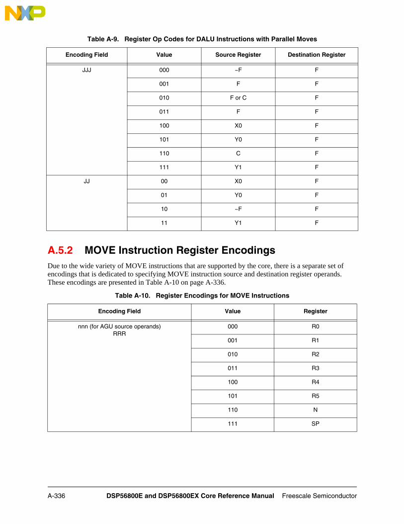
A.5.2 MOVE Instruction Register EncodingsDue to the wide variety of MOVE instructions that are supported by the core, there is a separate set of encodings that is dedicated to specifying MOVE instruction source and destination register operands. These encodings are presented in Table A-10 on page A-336.
Table A-9. Register Op Codes for DALU Instructions with Parallel Moves
Encoding Field Value Source Register Destination Register
JJJ 000 ~F F
001 F F
010 F or C F
011 F F
100 X0 F
101 Y0 F
110 C F
111 Y1 F
JJ 00 X0 F
01 Y0 F
10 ~F F
11 Y1 F
Table A-10. Register Encodings for MOVE Instructions
Encoding Field Value Register
nnn (for AGU source operands)RRR
000 R0
001 R1
010 R2
011 R3
100 R4
101 R5
110 N
111 SP
A-336 DSP56800E and DSP56800EX Core Reference Manual Freescale Semiconductor

NNN 000 R0
001 R1
010 R2
011 R3
100 R4
101 R5
110 N
111 (Reserved)
SSS 000 R0
001 R1
010 R2
011 R3
100 R4
101 R5
110 N
111 (Reserved)
RR 00 R0
01 R1
10 R2
11 R3
GGG 000 A
001 B
010 C
011 A1
100 X0
101 Y0
110 B1
111 Y1
Table A-10. Register Encodings for MOVE Instructions (Continued)
Encoding Field Value Register
Freescale Semiconductor Instruction Set Details A-337

A.5.3 Encodings for Instructions that Support the Entire Register Set
Certain core instructions can be performed on any register in the entire register set. These include certain types of MOVE instructions, the bit-manipulation instructions, and the hardware looping instructions (including DO and REP).
One class of these instructions is MOVE instructions that operate differently depending on whether a value is being loaded from memory into a register or is being stored from a register into memory. The register encodings that are used with this type of instruction are given in Table A-11.
GGGG 0000 A
0001 B
0010 C
0011 A1
0100 X0
0101 Y0
0110 B1
0111 Y1
1000 R0
1001 R1
1010 R2
1011 R3
1100 R4
1101 R5
1110 N
1111 (Reserved)
Table A-10. Register Encodings for MOVE Instructions (Continued)
Encoding Field Value Register
A-338 DSP56800E and DSP56800EX Core Reference Manual Freescale Semiconductor

Table A-11. Encodings for Instructions with Different Load and Store Register Sets
Encoding Field ValueRegister
Load Operation Store Operation
DDDDD(data ALU registers)
00000 A A1
00010 B B1
00100 C C1
00110 D D1
01000 X0 X0
01010 Y0 Y0
01100 (Reserved) Y
01110 Y1 Y1
DDDDD(accumulator registers)
00001 A1 A
00011 B1 B
00101 C1 C
00111 D1 D
01001 A2 A2
01011 B2 B2
01101 A0 A0
01111 B0 B0
DDDDD(AGU registers)
10000 R0 R0
10010 R1 R1
10100 R2 R2
10110 R3 R3
11000 R4 R4
11010 R5 R5
11100 N N
11110 (Reserved) (Reserved)
Freescale Semiconductor Instruction Set Details A-339

The second class of instructions that can specify any register consists of the bit-manipulation instructions. The encodings that are employed by these instructions are shown in Table A-12.
DDDDD(other registers)
10001 SP SP
10011 N3 N3
10101 M01 M01
10111 HWS HWS
11001 OMR OMR
11011 SR SR
11101 LC LC
11111 LA LA
Table A-12. Bit-Manipulation Register Encodings
Encoding Field Value Register
ddddd(general data ALU registers)
00000 A
00001 B
00010 C
00011 D
00100 X0
00101 Y0
00110 (Reserved)
00111 Y1
ddddd(AGU registers)
01000 R0
01001 R1
01010 R2
01011 R3
01100 R4
01101 R5
01110 N
01111 (Reserved)
Table A-11. Encodings for Instructions with Different Load and Store Register Sets (Continued)
Encoding Field ValueRegister
Load Operation Store Operation
A-340 DSP56800E and DSP56800EX Core Reference Manual Freescale Semiconductor

The final class of instructions that can specify any register in the core register set consists of MOVE instructions that access different portions of a register depending on the size of the data value that is being moved. Table A-13 on page A-342 shows the register operand encodings for this type of instruction.
ddddd(accumulator component registers)
10000 A1
10001 B1
10010 C1
10011 D1
10100 A2
10101 B2
10110 A0
10111 B0
ddddd(miscellaneous registers)
11000 SP
11001 N3
11010 M01
11011 HWS
11100 OMR
11101 SR
11110 LC
11111 LA
Table A-12. Bit-Manipulation Register Encodings (Continued)
Encoding Field Value Register
Freescale Semiconductor Instruction Set Details A-341

Table A-13. Size-Dependent Register Encodings for MOVE Instructions
Encoding Field ValueByte and Word Access Long-Word Access
Load Store Load Store
hhh 000 A A1 A A10
001 B B1 B B10
010 C C1 C C10
011 D D1 D D10
100 X0 X0 (Reserved) (Reserved)
101 Y0 Y0 (Reserved) (Reserved)
110 (Reserved) Y (Reserved) (Reserved)
111 Y1 Y1 Y Y
hhhh 0000 A A1 A A10
0001 B B1 B B10
0010 C C1 C C10
0011 D D1 D D10
0100 X0 X0 (Reserved) (Reserved)
0101 Y0 Y0 (Reserved) (Reserved)
0110 (Reserved) Y (Reserved) (Reserved)
0111 Y1 Y1 Y Y
1000 R0 R0 R0 R0
1001 R1 R1 R1 R1
1010 R2 R2 R2 R2
1011 R3 R3 R3 R3
1100 R4 R4 R4 R4
1101 R5 R5 R5 R5
1110 N N N N
1111 (Reserved) (Reserved) (Reserved) (Reserved)
A-342 DSP56800E and DSP56800EX Core Reference Manual Freescale Semiconductor

A.5.4 Parallel Move EncodingSome instructions support a parallel move or dual parallel read in conjunction with some other operation. These instructions encode the source and destination registers for the parallel move or dual parallel read separately from the registers that are used in the core operations. This section presents the encoding fields that are used to specify the registers that are accessed in the parallel move portion of the instruction.
Instructions with a single parallel move of the forms “X:<ea_m>,GGG” and “GGG,X:<ea_m>” encode the source or destination register using the values given in Table A-14 on page A-344.
dddd1 0000 A2 A2
0001 B2 B2
0010 C2 C2
0011 D2 D2
0100 X0 X0
0101 Y0 Y0
0110 LC2 LC2
0111 Y1 Y1
1000 SP SP
1001 N3 N3
1010 M01 M01
1011 HWS HWS
1100 OMR OMR
1101 SR SR
1110 LC LC
1111 LA LA
1.This encoding is only used for 32-bit stack push and pop operations.
Table A-13. Size-Dependent Register Encodings for MOVE Instructions (Continued)
Encoding Field ValueByte and Word Access Long-Word Access
Load Store Load Store
Freescale Semiconductor Instruction Set Details A-343

The encoding for dual parallel reads is given in Table A-15.
Table A-14. Single Parallel Move Register Encoding
Encoding Field Value Register
GGG 000 A
001 B
010 C
011 A1
100 X0
101 Y0
110 B1
111 Y1
Table A-15. Dual Parallel Read Encoding
Encoding Field Value Primary Read Secondary Read
vvvv 0000 X:(R0),Y0 X:(R3)+,X0
0100 X:(R0),Y0 X:(R3)–,X0
1000 X:(R0),Y1 X:(R3)+,X0
1100 X:(R0),Y1 X:(R3)–,X0
0001 X:(R1),Y0 X:(R3)+,X0
0101 X:(R1),Y0 X:(R3)–,X0
1001 X:(R1),Y1 X:(R3)+,X0
1101 X:(R1),Y1 X:(R3)–,X0
0010 (Reserved)
0110 (Reserved)
1010 X:(R0),Y1 X:(R3)+,C
1110 X:(R0),Y1 X:(R3)+N3,C
0011 X:(R4),Y0 X:(R3)+,X0
0111 X:(R4),Y0 X:(R3)+N3,X0
1011 X:(R4),Y1 X:(R3)+,C
1111 X:(R4),Y1 X:(R3)+N3,C
A-344 DSP56800E and DSP56800EX Core Reference Manual Freescale Semiconductor

A.5.5 Addressing Mode EncodingsThe instructions that support a parallel move or dual parallel read must specify the addressing mode that is used for the memory access or accesses. The encoding that is used to select the addressing mode is given in Table A-16..
A.5.6 Conditional Instruction EncodingThe conditional branch, jump, and register-transfer instructions are encoded differently depending on the condition specified. The encodings for the different conditions that are supported by the Tcc instruction are presented in Table A-17.
The encoding for the conditions that are used in the conditional branch and jump instructions is given in Table A-18 on page A-346.
Table A-16. Addressing Mode Encodings
Encoding Field Value Addressing Mode
MM 00 (Rn)+ or (SP)+
01 (Rn+N) or (SP+N)
10 (Rn)– or (SP)–
11 (Rn) or (SP)
m 0 (Rn)+
1 (Rn)+N
Table A-17. Condition Encoding for the Tcc Instruction
Encoding Field Value Condition
CCC 000 cc
001 cs
010 ne
011 eq
100 ge
101 lt
110 gt
111 le
Freescale Semiconductor Instruction Set Details A-345

A.5.7 Immediate and Absolute Address EncodingA number of core instructions specify one operand using an immediate value or absolute address. These values are encoded into the instruction using the following encoding fields:
• AAAAAA: 6-bit positive offset for X:(R2+xx) addressing mode. Allows positive offsets: 0 to 63.
• AAA: Top 3 address bits for 19-bit JMP, Jcc, and JSR instructions.
• AA: Top 2 address bits for 18-bit BRA, Bcc, and BSR instructions.
• Aaaaaaa: 7-bit signed offset for Bcc <OFFSET> and BRSET and BRCLR instructions. The U bit in BRSET and BRCLR instructions is used to indicate if the mask corresponds to the upper byte (U = 1) or the lower byte (U = 0). Aaaaaaa must never be all zeros when it is used with the Bcc instruction.
• aaaaaa: 6-bit negative offset for the X:(SP–xx) addressing mode. Allows negative offsets from –1 to –64.
• BBBBBBB: 7-bit signed integer that is used by an instruction whose operands are of the form “#<xx>,hhhh” or “#<xx>,F1”.
• BBBBBB: 6-bit unsigned integer that is used for DO and REP instructions. BBBBBB cannot be zero for DO loops.
Table A-18. Condition Encoding for Jump and Branch Instructions
Encoding Field Value Condition
CCCC 0000 cc (same as hs—unsigned higher or same)
0001 cs (same as lo—unsigned lower)
0010 ne
0011 eq
0100 ge
0101 lt
0110 gt
0111 le
1000 (Reserved)
1001
1010
1011
1100 hi (unsigned higher)
1101 ls (unsigned lower or same)
1110 nn
1111 nr
A-346 DSP56800E and DSP56800EX Core Reference Manual Freescale Semiconductor

• BBBBB: 5-bit signed integer for some data ALU and MOVE instructions.
• iii: 3-bit offset for X:(Rn+x) and X:(SP–x) addressing modes. Allows positive offsets for the X:(Rn+x) address mode from 0 to 7, and negative offsets from –1 to –8 for the X:(SP–x) addressing mode. See Table A-19.
• iiii: 4-bit unsigned integer for AGU arithmetic calculations and the MOVE.L #xx,hhh instruction.
• Ppppppp: 7-bit absolute address for MOVE, data ALU, and bit-manipulation instructions using the X:<<pp addressing mode. It is sign extended to allow access to both the peripherals and the first 64 locations in X memory.
Table A-19. Offset Values for iii Encoding
Encoded Value X:(Rn+x) Offset X:(SP–x) Offset
000 0 –8
001 1 –7
010 2 –6
011 3 –5
100 4 –4
101 5 –3
110 6 –2
111 7 –1
Freescale Semiconductor Instruction Set Details A-347

A-348 DSP56800E and DSP56800EX Core Reference Manual Freescale Semiconductor

Appendix BCondition Code Calculation
The execution of DSC core instructions, in addition to performing the selected task, often updates other state information in the execution core. The condition code bits in the status register (SR) reflect this state, which can in turn affect the execution of subsequent instructions.
This appendix contains information on condition code calculation for each instruction in the instruction set. It supplements the information given in Section 5.7, “Condition Code Calculation,” on page 5-38, which should be consulted for additional information.
B.1 Factors Affecting Condition Code CalculationIn general, condition codes are calculated according to very simple rules. However, the exact calculation can be affected by a number of factors. The size and type of operands that are used for a calculation, the current condition code mode, and the operation of the MAC output limiter can all affect the way condition codes are calculated. Each of these issues is discussed separately in the following sections.
B.1.1 Operand Size and TypeIn order to understand how condition codes are calculated, it is important to understand how arithmetic calculations are performed by the core. Depending on the size of the operands that are being used, the values that are used for computation are sign extended or zero extended internally, and the condition codes are based on the internal size that is used for calculation.
Operations in the data ALU are always performed with either 20- or 36-bit quantities. Operands that are not 20 or 36 bits in size are internally extended before the computation is performed. This extension occurs according to the same rules for alignment and extension that are used when values are loaded into an accumulator. Figure B-1 on page B-2 shows the alignment and extension that are performed.
Freescale Semiconductor Condition Code Calculation B-1

Figure B-1. Internal Data ALU Alignment and Extension
Once extension and alignment is done, a 20- or 36-bit calculation is performed, and the result is stored based on the destination size that is encoded in the opcode.
AGU operations are always performed using 24-bit quantities, and they always generate 24-bit results. Logic in the AGU automatically extends operands that are smaller than 24 bits in size, based on the type of operand specified. Figure B-2 shows the rules for extension based on the type of operand that is specified.
Figure B-2. Internal AGU Alignment and Extension
16-Bit OperandsSign
Extension Zero Fill
8-Bit Operands Sign Extension Zero Fill
035 32 1631 15
035
5-Bit Immediate Operands Zero Extension Zero Fill
16 1521 20
32-Bit OperandsSign
Extension
035 32 31
035 16 1524 23
36-Bit Operands
035
20-Bit Operands Zero Fill
035 16 15
17-Bit Immediate Operands
16-Bit Register Operands
6-Bit Immediate Operands
01623 15
01723 16
4-Bit Immediate Operands
4 3
24-Bit Operands
023
023
023
6 5
ZeroExtension
ZeroExtension
SignExtension
SignExtension
16-Bit Immediate Operands
01623 15
ZeroExtension
B-2 DSP56800E and DSP56800EX Core Reference Manual Freescale Semiconductor

B.1.2 MAC Output LimiterThe core contains a MAC output limiter that can be enabled to perform automatic saturation on the results of many data ALU operations before they are stored back into an accumulator. When saturated, results are limited to fit within the FF1:FF0 portion of the accumulator, with the extension portion containing only sign extension. Because results are limited to 32 bits, condition code calculation can be affected. The MAC output limiter is enabled through setting the SA bit in the operating mode register (OMR).
The following bits are affected by the MAC output limiter:
• U—Cleared if saturation occurs in the MAC output limiter
• V—Set when saturation occurs in the MAC output limiter
The following bits are only affected in unusual cases:
• L—May be indirectly affected through effects on V bit
• N—Affected only when ASRAC, LSRAC, or IMPY.W are executed
• C—Affected only by ASL
Condition code calculation is not affected by the MAC output limiter for most test and comparison instructions. However, it is possible for the MAC output limiter to affect the calculation of the U bit when the CMP.W instruction is executed. See Section B.3, “Condition Code Summary by Instruction,” for more information.
The MAC output limiter only affects operations in the data ALU. Move instructions, bit-manipulation instructions, and AGU instructions are not affected. See Section 5.8.3, “Instructions Not Affected by the MAC Output Limiter,” on page 5-42 for a complete list of data ALU instructions that are not affected.
NOTE:
When the MAC output limiter is enabled, condition codes are not alwaysset in an intuitive manner. It is best to examine each instruction todetermine the effect of the MAC output limiter on condition codecalculation.
B.1.3 Condition Code ModeThe data ALU’s condition code mode also affects condition code calculation. There are two condition code modes: 36-bit mode, where the extension portion of the accumulator (the FF2 portion) is used when condition codes are calculated, and 32-bit mode, where the extension registers are ignored. The mode is selected using the condition code mode bit (CM) in the OMR. When this bit is set, 32-bit mode is selected, and the accumulator extension registers are ignored when condition codes are calculated. When the CM bit is cleared, 36-bit condition code mode is used.
Signed values can be computed in either way, but pay attention to the condition code mode when performing unsigned operations. For correct operation, 32-bit condition code mode (CM bit set) must be selected when TST and CMP instructions are executed before jump and branch instructions that use the HI, HS, LO, or LS branch and jump conditions.
The condition code mode directly affects the following condition code bits:
• V—Set based on the MSB of the result’s MSP portion versus the extension portion
• Z—Set using only the MSP and LSP portions of the result versus the whole accumulator
Freescale Semiconductor Condition Code Calculation B-3

The following bits are only affected by the condition code mode in unusual cases:
• L—May be indirectly affected through effects on V bit
• N—Only affected by ASRAC, LSRAC, IMPY.W, and ASLL.W
• C—Only affected by ASL
The condition code mode does not affect any of the test and comparison instructions, such as TST.W and CMP.BP. The condition code mode also only affects operations performed in the data ALU. It does not affect operations that are performed outside the data ALU, such as move instructions, bit-manipulation instructions, and AGU instructions.
NOTE:
Because of enhancements to the instruction set, it is generally notnecessary to operate the DSC in 32-bit condition code mode. Newinstructions support test and compare operations for byte, word, and longdata types, as well as for full 36-bit accumulators. New applications shouldnot use 32-bit condition code mode.
B.2 Condition Code RegisterA description of each of the bits in the status register is given in the following sections. Each description given is the standard definition for each condition code bit, but the bits might be set or cleared slightly differently depending on the instruction being executed. For the exact calculation for a given instruction, see Section B.3, “Condition Code Summary by Instruction.”
The condition code register occupies the low-order 8 bits of the status register (SR).
SR Status RegisterBIT 15 14 13 12 11 10 9 8 7 6 5 4 3 2 1 BIT 0
LF P4 P3 P2 P1 P0 I1 I0 SZ L E U N Z V C
TYPE rw r r r r r rw rw rw rw rw rw rw rw rw rw
RESET 0 0 0 0 0 0 1 1 0 0 0 0 0 0 0 0
Table B-1. Condition Code Bit Descriptions1
Name Description Settings
SZBit 7
Size—Indicates growth beyond a certain point in the size of an accumulator value
0 = Accumulator value is small.1 = Accumulator value is large.
LBit 6
Limit—Indicates whether data limiting has been performed since this bit was last cleared
0 = No limiting performed.1 = Limiting has been performed.
EBit 5
Extension in Use—Indicates whether an accu-mulator extension register is in use
0 = Extension not in use.1 = Extension in use.
UBit 4
Unnormalized—Shows whether a result value is normalized or not
0 = Normalized.1 = Not normalized.
NBit 3
Negative—Indicates whether result of last oper-ation was negative or positive
0 = Result was positive.1 = Result was negative.
B-4 DSP56800E and DSP56800EX Core Reference Manual Freescale Semiconductor

The condition code bits are updated automatically after each instruction is executed according to the rules that are outlined in the following sections. Be careful when changing the values of the condition code bits under program control, because the state of the condition code bits can affect the execution of subsequent instructions.
B.2.1 Size Bit (SZ)The SZ bit is a latching bit (sticky bit) that indicates that word growth is occurring in an algorithm. It is set when a 36-bit accumulator is written to data memory if bits 30 and 29 of the source accumulator that is used in the move operation are not the same—that is, if both are not ones or zeros. SZ is not affected otherwise.
The SZ bit is designed for use in the FFT algorithm. It indicates that the next pass in the algorithm should scale its results before computation, allowing FFT data to be scaled only on passes where necessary, which in turn helps guarantee maximum accuracy in an FFT calculation.
The exact algorithm for calculating SZ is:
SZ = SZ | (Bit 30 ⊕ Bit 29)
The calculation of SZ is not affected by the condition code mode or by the operation of the MAC output limiter. The SZ bit is latched once it is set, and it is cleared only by processor reset or by an instruction that explicitly clears it.
B.2.2 Limit Bit (L)The limit bit (L) is a latching bit (sticky bit) that indicates that overflow has occurred in a data ALU operation or that limiting has occurred when one of the four accumulators (A, B, C, D) is moved with a single move or through a parallel move.
L = L | V | (limiting due to a move)
L is not affected otherwise. The calculation of L is not directly affected by either the MAC output limiter or the condition code mode. However, the MAC output limiter and the condition code mode do affect the calculation of the overflow (V) bit, which may indirectly affect the calculation of L.
The TFR and TFRA instructions are register-to-register transfer instructions and are not considered “move” instructions in the equation for calculating L. As a result, neither instruction will set the L bit, even if saturation is enabled (SA = 1) and saturation occurs. Note that the TFR instruction can set the L bit if it has a parallel move and if limiting occurs in that parallel move.
ZBit 2
Zero—Indicates whether result of last operation was zero or not
0 = Result was non-zero.1 = Result was zero.
VBit 1
Overflow—Indicates whether result of last oper-ation overflowed its destination
0 = Did not overflow.1 = Overflowed destination.
CBit 0
Carry—Set if a carry out or borrow was gener-ated in addition or subtraction
0 = No carry occurred during operation.1 = Carry-out occurred during operation.
1.For descriptions of bits 15–8 of the SR, see Table 8-2 on page 8-8.
Table B-1. Condition Code Bit Descriptions1 (Continued)
Name Description Settings
Freescale Semiconductor Condition Code Calculation B-5

The L bit is latched once it is set, and it is cleared only by processor reset or by an instruction that explicitly clears it.
B.2.3 Extension in Use Bit (E)The extension in use bit (E) indicates whether the extension portion of a data ALU result contains significant bits or whether they are just sign extension. If E is cleared, then bits 35–31 of the result are 00000 or 11111. E is set otherwise.
The E bit is calculated based on the 20- or 36-bit internal result that is computed by the data ALU. E is thus calculated regardless of whether the specified destination contains an extension register. See Section B.1.1, “Operand Size and Type,” for more information on how the internal result is calculated.
The calculation of E is not affected by the condition code mode. If the MAC output limiter is enabled, the E bit is set based on the result before it passes through the limiter. Saturation that occurs in the MAC output limiter can result in the E bit being set even though the final result does not use the extension portion of the accumulator.
B.2.4 Unnormalized Bit (U)The unnormalized bit (U) is set to indicate that the result of a data ALU operation is not normalized. It is set if the 2 most significant bits of the MSP of the result are the same, and it is cleared otherwise. The exact computation is as follows:
U = (Bit 31 ⊕ Bit 30) for 20-, 32-, and 36-bit calculations
U = (Bit 15 ⊕ Bit 14) for 8- and 16-bit calculations
U is not affected by the condition code mode. When the MAC output limiter is enabled, and when limiting is performed, this bit is always cleared. If no limiting is done by the MAC output limiter, U is computed using the preceding equations.
In general, the calculation of the U bit when a CMP.W instruction is executed is not affected by the state of the MAC output limiter. However, if the first operand to CMP.W is not a register (that is, it is a memory location or an immediate value), and if the second operand is X0, Y0, or Y1, then the calculation of U can be affected if the MAC output limiter is enabled.
B.2.5 Negative Bit (N)The negative bit (N) indicates whether or not the result of a data ALU or an AGU calculation is negative. A value is considered negative if the MSB of the result is set. Note that N is set based on the size of the destination for the result, not on the internal (20- or 36-bit) size.
The condition code mode has no effect on the calculation of N for 8-, 16-, 24-, and 32-bit results. For 20- or 36-bit results, N is based on bits 15 or 31 (respectively) if 32-bit condition code mode is selected. When saturation is enabled (SA = 1), the N bit is set based on the result before it passes through the MAC output limiter.
Calculation of the N bit is somewhat different for the ASLL.W, ASLL.L, ASRAC, LSRAC, and IMPY.W instructions. See Section B.3.3, “Special Calculation Rules for Certain Instructions,” for more information.
B-6 DSP56800E and DSP56800EX Core Reference Manual Freescale Semiconductor

B.2.6 Zero Bit (Z)The zero bit (Z) is set if the result of a data ALU or an AGU operation is zero. A value is zero if all significant bits are clear. The accumulator extension registers are not checked if 32-bit condition code mode is active.
B.2.7 Overflow Bit (V)The overflow bit (V) is set if an arithmetic overflow occurs in the result of a data ALU operation. Overflow occurs when the carry into the result’s MSB is not equal to the carry out of the MSB. This inequality indicates that the result of the ALU operation is not representable in the destination and that the result has overflowed. The V bit is set based on the size of the destination operand, not on the internally calculated (20- or 36-bit) value. If 32-bit condition code mode is selected, the extension portion of the destination is ignored.
When saturation is enabled (SA = 1), V is set when saturation occurs. If saturation does not occur, the preceding rules determine the V bit.
B.2.8 Carry Bit (C)The carry bit (C) is set if a carry is generated out of the most significant bit (MSB) of the result for an addition, or if a borrow is generated in a subtraction. It is cleared otherwise. C is always calculated based on a carry or borrow out of the high-order bit (bit 31 for a 32-bit result). Note that for 20- and 36-bit accumulator results, this bit will always be bit 35.
C is also used by a number of instructions to indicate conditions other than a carry out. The shift and rotate instructions place the bit that is shifted or rotated out of the destination into the carry bit. The C bit is also used by the bit-manipulation instructions to indicate the status of a bitfield comparison. See Table B-3 on page B-9 for more information.
Freescale Semiconductor Condition Code Calculation B-7

B.3 Condition Code Summary by InstructionA summary of condition code generation for every instruction appears in Table B-3 on page B-9. Note that the condition code computations shown in Table B-3 may differ from those given in the individual instruction descriptions in Appendix A, “Instruction Set Details.” In general, Table B-3 gives the core implementation viewpoint, while the instruction descriptions give the user viewpoint.
B.3.1 NotationTable B-2 presents the notation that is used in Table B-3 on page B-9.
B.3.2 Condition Code Calculation TableTable B-3 on page B-9 lists the computation for the condition code bits for each instruction, using the notation that is outlined in Table B-2. Any unusual condition code calculation, or changes to bits in the upper half of the status register, are noted in the “Comments” column.
Table B-2. Condition Code Summary Table Notation
Notation Description
* Set by the result of the operation according to the standard definition.
— Not affected by the operation.
*8 Set by the result of the operation according to the definition for 8-bit results in Section B.2, “Condition Code Register.”
*16 Set by the result of the operation according to the definition for 16-bit results in Section B.2, “Condition Code Register.”
*32 Set by the result of the operation according to the definition for 32-bit results in Section B.2, “Condition Code Register.”
*36 Set by the result of the operation according to the definition for 36-bit results in Section B.2, “Condition Code Register.”
*xx Set by the result of the operation according to the size of destination. This instruction can manipulate operands that are of different sizes.
=0 Cleared.
=1 Set.
? Set according to a special computation defined for the operation.
V L bit is set if overflow has occurred in result.
T L bit is set if limiting occurs when an accumulator is read during a parallel move or by the instruction itself. An example of the latter case is BFCHG #$8000,A, which must first read the A accumulator before performing the bit-manipulation operation.
VT L bit is set if overflow has occurred in result or if limiting occurs when an accumulator is read.
B-8 DSP56800E and DSP56800EX Core Reference Manual Freescale Semiconductor

Table B-3. Condition Code Summary (Sheet 1 of 5)
Instruction SZ L E U N Z V C Comments
ABS * VT *36 *36 *36 *36 *36 —
ADC — V *36 *36 *36 *36 *36 *36
ADD * VT *xx *xx *xx *xx *xx *xxADD.B — — *8 *8 *8 *8 *8 *8
ADD.BP — — *8 *8 *8 *8 *8 *8
ADD.L — — *32 *32 *32 *32 *32 *32
ADD.W — V *xx *xx *xx *xx *xx *xxADDA — — — — — — — —
ADDA.L — — — — — — — —
ALIGNSP — — — — — — — —AND.L — C — — *32 *32 =0 —
AND.W — — — — *16 *16 =0 —
ASL * VT *xx *xx *xx *xx ? ? See Section B.3.3.1, “ASL and ASL.W,” for informa-tion on the V and C bits.
ASL.W — VT *16 *16 *16 *16 ? ? See Section B.3.3.1, “ASL and ASL.W,” for informa-tion on the V and C bits.
ASL16 — — — — — — — —ASLA — — — — — — — —
ASLL.L — — — — ? *32 — — See Section B.3.3.2, “ASLL.W and ASLL.L,” for infor-mation on how the N bit is set.
ASLL.W — — — — ? *32 — — See Section B.3.3.2, “ASLL.W and ASLL.L,” for infor-mation on how the N bit is set.
ASR * T *xx *xx *xx *xx =0 ? C is set to the value in the LSB of the source operand prior to the operation.
ASR16 — — — — — — — —
ASRA — — — — — — — —ASRAC — — — — ? *36 — — If the OMR’s SA bit is one, then the N bit is equal to
bit 31 of the result. If SA is zero, then N is equal to bit 35 of the result.
ASRR.L — — — — *32 *32 — —ASRR.W — — — — *32 *32 — —
Bcc — — — — — — — —
BFCHG — T — — — — — ? See Section B.3.3.4, “BFCHG, BFCLR, BFSET, BFT-STH, and BRSET.”
BFCLR — T — — — — — ? See Section B.3.3.4, “BFCHG, BFCLR, BFSET, BFT-STH, and BRSET.”
BFSC — T — — — — — ? See Section B.3.3.6, “BFSC.” BFSET — T — — — — — ? See Section B.3.3.4, “BFCHG, BFCLR, BFSET, BFT-
STH, and BRSET.” BFTSTH — T — — — — — ? See Section B.3.3.4, “BFCHG, BFCLR, BFSET, BFT-
STH, and BRSET.” BFTSTL — T — — — — — ? See Section B.3.3.5, “BFTSTL and BRCLR.”
BRA — — — — — — — —
BRAD — — — — — — — —
BRCLR — T — — — — — ? See Section B.3.3.5, “BFTSTL and BRCLR.” BRSET — T — — — — — ? See Section B.3.3.4, “BFCHG, BFCLR, BFSET, BFT-
STH, and BRSET.” BSR — — — — — — — —
CLB — — — — *16 *16 =0 —
CLR * VT *36 *36 *36 *36 *36 —
Freescale Semiconductor Condition Code Calculation B-9

CLR.B — — — — — — — —
CLR.BP — — — — — — — —CLR.L — — — — — — — —
CLR.W — — — — — — — —
CMP * VT *xx *xx *xx *xx *xx *xx
CMP.B — — *8 *8 *8 *8 *8 *8CMP.BP — — *8 *8 *8 *8 *8 *8
CMP.L — — *32 *32 *32 ? *32 *32 If the destination is a 16-bit register, the Z bit is set based on the LSP of the result. Otherwise, the Z bit is set based on the full 32-bit quantity.
CMP.W — V *16 ? *16 *16 *16 *16 If the SA bit is set, if the first operand is not a register, and if the second operand is Y1, Y0, or X0, the U bit is cleared if saturation occurs during the comparison. Otherwise, the normal definition for the U bit is used.
CMPA — — — — *24 *24 *24 *24
CMPA.W — — — — *16 *16 *16 *16DEBUGEV — — — — — — — —
DEBUGHLT — — — — — — — —
DEC.BP — — *8 *8 *8 *8 *8 *8DEC.L — — *32 *32 *32 *32 *32 *32
DEC.W * VT *xx *xx *xx *xx *xx *xx
DECA — — — — — — — —DECA.L — — — — — — — —
DECTSTA — — — — *24 *24 *24 *24
DIV — V — — — — ? ? V is set if the MSB of the destination operand is changed as a result of the left shift; it is cleared other-wise. V is not affected by SA or CM.C is set if the MSB of the result is zero; it is cleared otherwise.
DO — T — — — — — — Affects LF and NL bits.DOSLC — — — — — — — — Affects LF and NL bits.
ENDDO — — — — — — — — Condition Codes are not affected by this instruction.
EOR.L * T — — *32 *32 =0 —EOR.W — — — — *16 *16 =0 —
FRTID Restored from the FISR register See Section 9.3.2.2, “Fast Interrupt Processing,” on page 9-6.
ILLEGAL — — — — — — — — Sets I1 and I0 bits in the SR.
IMAC32 — V *xx *xx *xx *xx *xx —IMAC.L — V *xx *xx *xx *xx *xx —
IMACUS — — — — — — — —
IMACUU — — — — — — — —IMPY32 — V *xx *xx *xx *xx =0 — L is unchanged.
IMPY64 — V *xx *xx *xx *xx =0 — L is unchanged.
IMPY64UU — — — — — — — —
IMPY.L — V *xx *xx *xx *xx =0 — L is unchanged.IMPY.W — V — — ? *16 *16 — See Section B.3.3.7, “IMPY.W,” for information on
how the N bit is set.IMPYSU — — — — — — — —
IMPYUU — — — — — — — —
INC.BP — — *8 *8 *8 *8 *8 *8
Table B-3. Condition Code Summary (Sheet 2 of 5)
Instruction SZ L E U N Z V C Comments
B-10 DSP56800E and DSP56800EX Core Reference Manual Freescale Semiconductor

INC.L — — *32 *32 *32 *32 *32 *32
INC.W * VT *xx *xx *xx *xx *xx *xxJcc — — — — — — — —
JMP — — — — — — — —
JMPD — — — — — — — —
JSR — — — — — — — —LSL.W — — — — *16 *16 =0 ? C is set to the value in the MSB of the source oper-
and prior to the operation.LSR.W — — — — *16 *16 =0 ? C is set to the value in the LSB of the source operand
prior to the operation.LSR16 — — — — — — — —
LSRA — — — — — — — —
LSRAC — — — — ? *36 — — If the OMR’s SA bit is one, then the N bit is equal to bit 31 of the result. If SA is zero, then N is equal to bit 35 of the result.
LSRR.L — — — — *32 *32 — —
LSRR.W — — — — *32 *32 — —MAC * VT *xx *xx *xx *xx *xx —
MAC32 * VT *xx *xx *xx *xx *xx —
MACR * VT *xx *xx *xx *xx *xx —MACSU — V *xx *xx *xx *xx *xx —
MOVE.B — — — — — — — —
MOVE.BP — — — — — — — —MOVE.L — — — — — — — —
MOVE.W * T — — — — — —
MOVEU.B — — — — — — — —MOVEU.BP — — — — — — — —
MOVEU.W Corresponding source bits Not affected unless SR is specified as the destination in the instruction.
MPY * VT *xx *xx *xx *xx *xx — V is cleared.
MPY32 * VT *xx *xx *xx *xx *xx — V is cleared.MPY64 * VT *xx *xx *xx *xx *xx — V is cleared.
MPYR * VT *xx *xx *xx *xx *xx — V is cleared.
MPYSU — V *xx *xx *xx *xx *xx — V is cleared; L is unchanged.NEG * VT *xx *xx *xx *xx *xx *xx
NEG.BP — — *8 *8 *8 *8 *8 *8
NEG.L — — *32 *32 *32 ? *32 *32 If the destination is a 16-bit register, the Z bit is set based on the LSP of the result. Otherwise, the Z bit is set based on the full 32-bit quantity.
NEG.W — V *xx *xx *xx *xx *xx *xx
NEGA — — — — — — — —NOP — — — — — — — —
NORM — V *36 *36 *36 *36 ? — See Section B.3.3.8, “NORM.”
NOT.W — — — — *16 *16 =0 —
OR.L — — — — *32 *32 =0 —OR.W — — — — *16 *16 =0 —
REP — T — — — — — —
RND * VT *36 *36 *36 *36 *36 —
Table B-3. Condition Code Summary (Sheet 3 of 5)
Instruction SZ L E U N Z V C Comments
Freescale Semiconductor Condition Code Calculation B-11

ROL.L — — — — — — — ? C is set to the value in the MSB of the source oper-and prior to the operation.
ROL.W — — — — *16 *16 =0 ? C is set to the value in the MSB of the source oper-and prior to the operation.
ROR.L — — — — — — — ? C is set to the value in the LSB of the source operand prior to the operation.
ROR.W — — — — *16 *16 =0 ? C is set to the value in the LSB of the source operand prior to the operation.
RTI Restored from stack Updates P4–P0 bits in SR.
RTID Restored from stack Updates P4–P0 bits in SR.
RTS — — — — — — — — Updates P4–P0 bits in SR.RTSD — — — — — — — — Updates P4–P0 bits in SR.
SAT * VT — — — — — —
SBC — V *36 *36 *36 *36 *36 *36STOP — — — — — — — —
SUB * VT *xx *xx *xx *xx *xx *xx
SUB.B — — *8 *8 *8 *8 *8 *8SUB.BP — — *8 *8 *8 *8 *8 *8
SUB.L — — *32 *32 *32 *32 *32 *32
SUB.W — V *xx *xx *xx *xx *xx *xxSUBA — — — — — — — —
SUBL — — — — — — — —
SWAP — — — — — — — —SWI — — — — — — — — Affects I1 and I0 bits in SR.
SWI #x — — — — — — — — Affects I1 and I0 bits in SR.
SWILP — — — — — — — — Does not affect I1 and I0 bits in SR; no change.SXT.B — — — — — — — —
SXT.L — — — — — — — —
SXTA.B — — — — — — — —SXTA.W — — — — — — — —
Tcc — — — — — — — —
TFR * T — — — — — — Only via parallel move.TFRA — — — — — — — —
TST * VT *36 *36 *36 *36 =0 =0 On a data ALU register.
TST.B — — *8 *8 *8 *8 =0 =0 On a data ALU register.— — — — *8 *8 =0 =0 On a memory location.
TST.BP — — — — *8 *8 =0 =0 On a memory location.
TST.L — — *32 *32 *32 ? =0 =0 On a data ALU register. If the destination is a 16-bit register, the Z bit is set based on the LSP of the result. Otherwise, the Z bit is set based on the full 32-bit quantity.
— — — — *32 *32 =0 =0 On a memory location.
TST.W — V *16 *16 *16 *16 =0 =0 On a data ALU accumulator (FF).
— V — — *16 *16 =0 =0 On remaining data ALU registers.
— — — — *16 *16 =0 =0 On a memory location.TSTA.B — — — — *8 *8 =0 =0
TSTA.L — — — — *24 *24 =0 =0
TSTA.W — — — — *16 *16 =0 =0
Table B-3. Condition Code Summary (Sheet 4 of 5)
Instruction SZ L E U N Z V C Comments
B-12 DSP56800E and DSP56800EX Core Reference Manual Freescale Semiconductor

TSTDECA.W — — — — *16 *16 =0 *16 Condition codes based on test operation before the decrement occurs.
WAIT — — — — — — — —
ZXT.B — — — — — — — —ZXTA.B — — — — — — — —
ZXTA.W — — — — — — — —
Table B-3. Condition Code Summary (Sheet 5 of 5)
Instruction SZ L E U N Z V C Comments
Freescale Semiconductor Condition Code Calculation B-13

B.3.3 Special Calculation Rules for Certain InstructionsThere are a few instructions that cause the condition codes to be calculated in an unusual or non-intuitive way. The following subsections detail these instructions and their particular condition code calculations.
B.3.3.1 ASL and ASL.W
In general, V is set if the MSB of the destination operand (bit 35 for an accumulator; bit 31 for the Y register; or bit 15 for the X0, Y0, and Y1 registers) is changed as a result of the left shift. V is cleared otherwise. If the MAC output limiter is enabled and saturation occurs, V is set. If 32-bit condition code mode is selected (CM = 1), V is set to the value of the E bit after the operation occurs.
C is set to the value in the MSB of the source operand prior to the shift. For accumulator registers, the MSB is bit 35 when 36-bit condition code mode is used or bit 31 when 32-bit condition code mode is used. For the Y register, bit 31 is used. Bit 15 is the MSB for the X0, Y0, and Y1 registers.
B.3.3.2 ASLL.W and ASLL.L
If 32-bit condition code mode is selected (CM = 1), N is always cleared after either the ASLL.W or ASLL.L instructions are executed. Otherwise, it is calculated as described in Section B.2.5, “Negative Bit (N),” if 36-bit condition code mode is being used.
B.3.3.3 ASRAC and LSRAC
The calculation of N is somewhat unusual for the ASRAC and LSRAC instructions. When the MAC output limiter is disabled (SA = 0) and the data ALU is set to 36-bit condition code mode (CM = 0), the N bit is obtained from bit 35. If either 32-bit condition code mode is selected or saturation is enabled, the N bit is set based on bit 31 of the result before it passes through the MAC output limiter.
B.3.3.4 BFCHG, BFCLR, BFSET, BFTSTH, and BRSET
The carry bit (C) is set if all bits that are specified by the bit mask are set to one; it is cleared otherwise. Note that all the bits in the status register can be affected by BFCHG, BFCLR, and BFSET if the destination operand is the status register.
B.3.3.5 BFTSTL and BRCLR
The carry bit (C) is set if all bits that are specified by the bit mask are cleared (set to zero). It is cleared otherwise.
B.3.3.6 BFSC
The carry bit (C) is set if all bits specified by the value of the bit_select_mask match their associated value in the operation_mask. The carry bit (C) is cleared if at least 1 bit specified by the value of the bit_select_mask does not match its associated value in the operation_mask.
B-14 DSP56800E and DSP56800EX Core Reference Manual Freescale Semiconductor

B.3.3.7 IMPY.W
For the IMPY.W instruction, a 31-bit integer product is calculated internally, and the lowest 16 bits of this product are stored in the destination register. When the MAC output limiter is disabled and the data ALU is set to 36-bit condition code mode (CM = 0), the N bit is set to the value in bit 15 of the result. If either 32-bit condition code mode is selected or the MAC output limiter is enabled (SA = 1), the N bit is set to the value in bit 30 of the internally computed result. These two values differ only when the result overflows 16 bits.
V is set if the computed result does not fit in 16 bits and is cleared otherwise, regardless of the state of the SA and CM bits.
B.3.3.8 NORM
In general, the overflow bit (V) is set if the MSB of the destination operand (bit 35 for an accumulator; bit 31 for the Y register; or bit 15 for the X0, Y0, and Y1 registers) is changed as a result of the left shift. V is cleared otherwise. If the MAC output limiter is enabled and saturation occurs, V is set. If 32-bit condition code mode is selected (CM = 1), V is set to the value of the E bit after the operation occurs.
Freescale Semiconductor Condition Code Calculation B-15

B-16 DSP56800E and DSP56800EX Core Reference Manual Freescale Semiconductor

Appendix CGlossary
The following terms may be useful in understanding the material in this manual.
A/D analog-to-digitalThe process or characteristic of converting an analog signal into a digital representation of that signal. See also D/A.
ADC analog-to-digital converterA circuit that performs an analog-to-digital conversion. See also DAC.
AGU address generation unitThe functional block within a processor that performs address calculations and that provides memory access addresses.
ALU arithmetic logic unitThe functional block within a processor where arithmetic operations and logical operations are performed. These operations include addition, multiplication, logical AND and OR operations, shift and rotate operations, and so forth.
AMPS Advanced Mobile Phone ServiceA cellular transmission system that is fundamentally analog. AMPS transmits voice signals using an FM transmitter, just as a standard two-way radio does. The system performs call supervision functions (on hook, off hook, hook flash, and so on) with various analog signaling tones. However, AMPS signals for call setup with digital signaling. An important variation of this system is NAMPS, which Freescale developed.
ASIC Application Specific Integrated CircuitAn integrated circuit that is designed for a specific task and that performs that task. An ASIC cannot be reprogrammed to perform another task.
BGA ball grid arrayA flat ceramic or plastic package, usually square, that is used to hold an integrated circuit. The electrical leads, or pins, are located in a grid-like pattern on one of the flat sides, and the leads somewhat resemble hemispheres. A BGA is similar to a PGA.
BusAn electronic “traffic lane” that carries electrical signals through one chip to another chip. For example, an address bus takes the electrical signals that define a certain memory address and transfers them to a memory device (such as a RAM or ROM device).
CAS column address strobeThe signal that tells a memory device to accept the given address as a column address. CAS is used with RAS and a row address to select a bit within the device.
Freescale Semiconductor Glossary C-1

CDMA Code Division Multiple AccessCDMA is a digital wireless transmission standard that is used in mobile telephones. It is a form of spread-spectrum transmission, where the digitized voice is combined with a special code that allows several users to share the same portion of the radio spectrum. The different codes allow the various signals to be sorted at the receiving end. The current CDMA standard was developed by QUALCOMM.
CISC complex instruction set computingAn architectural design concept that is usually associated with microprocessors. CISC chips use instructions, or commands, that combine several steps into one.
CMOS complementary metal oxide semiconductorCMOS is the semiconductor technology that is used in the transistors that are manufactured into most microchips. CMOS transistors use almost no power when they are not needed.
CODEC COder/DECoderA part that is used to convert analog signals to digital (coder) and digital signals to analog (decoder).
COFF common object file formatA binary file format for storing compiled or assembled program data. COFF is used extensively by Unix- and Windows-based application development systems.
COP computer operating properlyA term that usually refers to a timer that is similar to a watchdog timer. Under normal operation, an application resets this timer periodically to indicate that the system is functioning normally. If the timer is allowed to expire, it usually resets the system to re-establish normal operation, on the assumption that something has gone wrong.
CPU central processing unitThe (usually) single integrated circuit (IC) that does the actual interpreting of program instructions and processing of data in a computer.
D/A digital-to-analogThe process or characteristic of converting a digital representation of a signal into an analog signal. See also A/D.
DAC digital-to-analog converterA circuit that performs a digital-to-analog conversion. See also ADC.
DMA direct memory accessA feature that allows peripheral systems to access memory for both read and write operations without the assistance of (and without affecting the state of) the processor.
DRAM dynamic random access memoryA type of memory component that is used to store information. “Dynamic” means the DRAM devices need a constant “refresh” (pulse of current through all of the memory cells) to keep the stored information.
DSL digital subscriber lineA communications technology that provides high-speed, two-way data communications over standard analog phone lines.
C-2 DSP56800E and DSP56800EX Core Reference Manual Freescale Semiconductor

DSC digital signal controllerDigital signal processing is the manipulation of analog information—such as sound, photographic images, or transmitted signals—that has been converted into a digital form. A digital signal controller, which is similar to a CPU, is a semiconductor device that is optimized for the mathematics that is performed in digital signal processing.
EEPROM electrically erasable PROMAn EEPROM is similar to an EPROM, but it can be erased by applying an erase current to the device, rather than by exposing it to ultraviolet light.
Enhanced On-Chip Emulation (Enhanced OnCE™)The Enhanced OnCE port is a Freescale-designed module that is used to debug application software that is used with the chip. The port is a separate on-chip block that allows non-intrusive interaction with the DSC and is accessible through the pins of the JTAG interface. The Enhanced OnCE port makes it possible to examine the contents of registers, memory, or on-chip peripherals in a special debug environment. No user-accessible resources need to be sacrificed to perform debugging operations.
EPROM erasable PROMA programmable, read-only memory device that can be erased by being exposed to ultraviolet light. EPROM devices maintain their contents even when electrical power is lost.
FIFO first in, first outA data structure or device in which data items are removed in the order in which they are added. The most common first-in-first-out data structure is called a queue. See also LIFO.
Flash memoryA type of non-volatile memory that retains data when power is removed. Flash memory devices are similar to EPROMs, with the exception that flash memory devices can be electrically erased (EPROMs must be exposed to ultraviolet light to be erased).
GPIO general-purpose input/outputAn input/output interface that is not dedicated to any particular task, but that can be used to transmit or receive data from a variety of other devices.
GSM Global System for Mobile Communications (previously Groupe Spécial Mobile)A TDMA communications system that also has frequency-hopping and encryption features. While TDMA is primarily a North American standard, GSM, which originated in Europe, is rapidly being deployed worldwide.
GUI graphical user interfaceA program interface that takes advantage of a computer's graphics capabilities to make the program easier to use.
IC integrated circuitAnother name for a computer chip. An IC is a small electronic device that is made of a semiconductor material.
ICE in-circuit emulatorA device that emulates a computer chip (typically a microprocessor) that can be used in place of a real chip in a computer to assist in testing and debugging.
iDEN Integrated Dispatch Enhanced NetworkA standard for wireless communications that was developed by Freescale, iDEN is based on the TDMA standard. It enhances TDMA by adding special modulation and encoding
Freescale Semiconductor Glossary C-3

technologies that increase efficiency and enable higher transmission speeds. Devices based on iDEN technology typically include multiple functions, such as telephony, paging, and radio.
IEEE Institute of Electrical and Electronics EngineersA technical professional association that focuses on disseminating information on electrical and electronics technologies. IEEE’s activities include drafting standards and specifications for all aspects of electronics and communications.
I/O input/outputI/O refers to any operation, program, or device whose purpose is to enter data into a processor or to extract data from a processor. The term can also be used to distinguish non-computational parts of a program from other parts that are strictly computational, or to distinguish devices or units. For example, a serial port is an I/O unit, whereas an ALU is a computational unit.
JTAG Joint Test Action GroupAn industry group that defined the IEEE standard for boundary-scan and test capabilities on an integrated circuit. The term JTAG is often used to refer to these capabilities, or to the test access port (TAP) that is used to access this test logic.
K&R Kernighan and RitchieThis abbreviation refers both to Brian Kernighan and Dennis Ritchie, the authors of The C Programming Language, and to the book itself. This book is considered to be the definitive reference text on the C language.
LIFO last in, first outA data structure or device in which data items are removed in the reverse order from that in which they are added, so the most recently added item is the first one to be removed. The most common form of a last-in-first-out data structure is a stack. See also FIFO.
LSB least significant bitThe lowest numbered bit in a multi-bit data value; it is almost always bit 0. See also MSB.
LSP least significant portionIn a multi-part value, the portion that occupies the lowest numbered bits. For example, in a 32-bit value that is composed of two 16-bit portions, the least significant portion would be the portion that occupies bits 15–0. See also MSP.
MAC multiply-accumulateAn operation that multiplies two numbers together and adds the product to a “running total.” Dedicated hardware to perform multiply-accumulate operations is common in digital signal controllers because DSC algorithms frequently perform this type of calculation. The term multiply-accumulate can also function as a verb, and MAC can refer to a unit that performs multiply-accumulate operations.
MCU microcontroller unitSimilar to a CPU, a microcontroller unit includes not only circuitry to execute instructions, but also peripheral modules and specialized interfaces. An MCU is typically used in embedded systems applications, while a CPU is found in general-purpose computers.
MIPS million instructions per secondA rough measure of processor performance, measuring the number of instructions that can be executed in one second. However, some instructions require more or less time than others to execute, and performance can be limited by other factors, such as memory and I/O speed.
C-4 DSP56800E and DSP56800EX Core Reference Manual Freescale Semiconductor

MOS metal oxide semiconductorA semiconductor manufacturing technology that is used to make the transistors that compose a microchip. This process is still used, but CMOS technology largely supersedes it.
MSB most significant bitThe highest bit in a value: bit 31 for a 32-bit value, bit 7 for an 8-bit value, and so forth. See also LSB.
MSP most significant portionIn a multi-part value, the portion that occupies the highest numbered bits. For example, in a 32-bit value that is composed of two 16-bit portions, the most significant portion would be the portion that occupies bits 31–16. See also LSP.
NAMPS Narrowband Advanced Mobile Phone ServiceA communications system, developed by Freescale, that is similar to AMPS. NAMPS uses a narrower bandwidth channel and low-speed digital signaling for call supervision, which increases efficiency and capacity as compared to AMPS.
OnCE™ On-Chip EmulationSee Enhanced On-Chip Emulation.
PAL programmable array logicA device that can be programmed to perform certain logic functions. Once the device is programmed, the programmed information can never be changed. Sometimes a PAL is called a PLD (programmable logic device).
PC program counterA register in a processor that holds the address of the next instruction to execute in a program.
PCS Personal Communications ServiceA telecommunications standard that is used in North America. PCS is virtually identical to the cellular standard, but it uses a different frequency.
PGA pin grid arrayA square, flat, ceramic or plastic package that is used to hold an integrated circuit. The electrical leads, or pins, are located in a grid-like pattern on one of the flat sides.
PLL phase-locked loopAn electronic circuit that controls an oscillator so that it maintains a constant phase angle relative to a reference signal. A PLL can be used to multiply or divide an input clock frequency to generate a different output frequency.
Pmem program (P) memoryThe memory space where program instructions are stored. See also Xmem.
PQFP plastic quad flat packA square, flat, plastic package that is used to hold an integrated circuit. The electrical leads, or pins, are located around all four sides of the package.
PROM programmable read-only memoryA read-only memory device whose contents are programmed using specialized equipment. The contents of the device are maintained even when electrical power is lost.
Freescale Semiconductor Glossary C-5

QFP quad flat packA flat, rectangular package that is used to hold an integrated circuit. The electrical leads, or pins, project from all four sides of the package. These packages are usually made of ceramic materials; when one is made of plastic, it is called a PQFP. A TQFP is another variation.
RAS row address strobeThe signal that tells a memory device to accept the given address as a row address. RAS is used with CAS and a column address to select a bit within the device.
RISC reduced instruction set computingAn architectural design concept that is usually associated with microprocessors. RISC chips use simpler instructions, or commands, than CISC chips. They need to use more steps to perform many functions that CISC chips perform in one step.
SDRAM synchronous dynamic random access memoryA type of DRAM that is capable of delivering bursts of data at very high speeds using a synchronous interface.
SP stack pointerA register inside a processor that holds the top address of a stack data structure in memory.
SPI serial peripheral interfaceA Freescale-standard communications interface. An SPI allows full-duplex, synchronous, serial communication between a processor and peripheral devices, including other processors. See also SSI.
SRAM static random access memoryA memory device that is similar to DRAM, with the exception that the memory does not need to be refreshed.
SSI synchronous serial interfaceA communications interface that is very similar to but more powerful than an SPI. For example, an SSI can use different clocks for receiving and transmitting data. SSIs are optimized for communication with CODECs.
TAP test access portAn interface that is used to access the JTAG-standard boundary-scan and test unit on an integrated circuit (typically a processor).
TDMA Time Division Multiple AccessTDMA is a digital wireless communications standard. Digitized voice communications are sent in bursts that are timed in such a way so as not to interfere with other stations that are using the same channel. An important variation of this system is GSM.
TQFP thin quad flat packSee QFP.
WAP wireless application protocolAn application environment and a set of communication protocols for wireless devices that is designed to enable manufacturer-, vendor-, and technology-independent access to the Internet and advanced telephony services.
Xmem data (X) memoryThe memory space in which data values (not program instructions) are stored. See also Pmem.
C-6 DSP56800E and DSP56800EX Core Reference Manual Freescale Semiconductor

Index
Symbols
# 3-26, 3-38< (forcing operator) 3-26<< (forcing operator) 3-26> (forcing operator) 3-26>> (forcing operator) 3-26
A
A, see accumulator registers (A, B, C, and D)A0, see least significant product registers (A0, B0, C0,
and D0)A1, see most significant product registers (A1, B1, C1,
and D1)A2, see extension registers (A2, B2, C2, and D2)ABS instruction 4-3, 4-31, 4-49, A-8accumulator data alignment 3-13accumulator extension registers, see extension registers
(A2, B2, C2, and D2)accumulator least significant product registers, see least
significant product registers (A0, B0, C0, and D0)
accumulator most significant product registers, see most significant product registers (A1, B1, C1, and D1)
accumulator registers (A, B, C, and D) 2-9, 3-2 to 3-3, 5-2, 5-4 to 5-6
bit-manipulation operations 5-14converting to 16-bit values 5-13extension registers, using 5-9notation 5-4 to 5-6, 5-9portions, accessing 5-9reading fractional values 5-12reading integer data 5-12saving and restoring 5-13writing integer data 5-12writing small operands 5-8
ADC instruction 4-3, 4-16, 4-31, A-10ADD instruction 4-3, 4-31, 4-49 to 4-50,
A-12 to A-15add with carry 4-31ADD.B instruction 4-3, 4-31, A-16ADD.BP instruction 4-3, 4-31, A-17ADD.L instruction 4-3, 4-32, A-19ADD.W instruction 4-3, 4-15, 4-32, A-21ADDA instruction 4-8, 4-13, 4-42, A-24ADDA.L instruction 4-8, 4-13, 4-42, A-26addition 5-16
Freescale Semiconductor Ind
fractional 5-16 to 5-17integer 5-16 to 5-17
address registers (R0–R5) 2-9, 6-3 to 6-4addressing mode remapping 4-13addressing modes 3-23
absolute 3-41address register indirect 3-28immediate 3-38implicit 3-45linear 6-20modulo 6-20post-update 3-30 to 3-32register direct 3-28
AGU arithmetic instructions 4-7, 4-42AGU registers 3-4
capabilities 6-6data alignment 3-14restrictions 6-6shifting 4-42
ALIGNSP instruction 4-8, 4-15, 4-48, 10-3, A-28ALU, see data arithmetic logic unit (data ALU)analog signal processing 1-5analog-to-digital conversion 1-5 to 1-6AND.L instruction 4-7, 4-41, A-29AND.W instruction 4-7, 4-41, A-31ANDC instruction 4-7, 4-12, 4-15 to 4-16, 7-1, A-33arithmetic instructions 4-3, 4-7arithmetic overflow 8-9ASL instruction 4-6, 4-39, 4-49 to 4-50, A-34, A-37ASL.W instruction 4-6, 4-39, A-34, A-37ASL16 instruction 4-6, 4-13, 4-39, A-39ASLA instruction 4-8, 4-13, 4-42, A-40ASLL.L instruction 4-6, 4-39, A-41ASLL.W instruction 4-6, 4-39, A-43ASR instruction 4-6, 4-39, 4-49 to 4-50, A-45ASR16 instruction 4-6, 4-13, 4-39, A-48 to A-49ASRA instruction 4-8, 4-42, A-50ASRAC instruction 4-6, 4-39, A-51ASRR.L instruction 4-6, 4-39, A-53ASRR.W instruction 4-6, 4-40, A-55
B
B, see accumulator registers (A, B, C, and D)B0, see least significant product registers (A0, B0, C0,
and D0)B1, see most significant product registers (A1, B1, C1,
and D1)B2, see extension registers (A2, B2, C2, and D2)
ex Index-i

Bcc instruction 4-11, 4-15, 4-46, 9-11, A-57 to A-58BFCHG instruction 4-9, 4-12, 4-15 to 4-16, 4-43, 7-1,
A-59BFCLR instruction 4-9, 4-12, 4-15 to 4-16, 4-44, 7-1,
A-62BFSET instruction 4-9, 4-12, 4-15 to 4-16, 4-44, 7-1,
A-65BFTSTH instruction 4-9, 4-44, 7-1, A-68BFTSTL instruction 4-9, 4-45, 7-1, A-71bit-manipulation instructions 4-9, 4-43, 7-1, 8-9BR1CLR operation 7-8 to 7-10BR1SET operation 7-8 to 7-10BRA instruction 4-11, 4-15, 4-46, A-74BRAD instruction 4-11, 4-14 to 4-15, 4-46, A-75BRCLR instruction 4-11, 4-45, 7-1, 7-9, 9-11, A-77breakpoints and breakpoint counter 11-8, 11-11BRSET instruction 4-11, 4-45, 7-1, 7-9, 9-11, A-80BSR instruction 4-11, 4-15, 4-46, 8-11, 8-15, A-83bus and bit-manipulation unit 7-1byte addresses 3-16, 6-7byte ordering 6-8byte pointers 3-18, 3-21 to 3-22, 6-4, 6-11, 6-13byte variable alignment 3-16
C
C programming language 1-2, 6-11C, see accumulator registers (A, B, C, and D) and carry
bit (C)C0, see least significant product registers (A0, B0, C0,
and D0)C1, see most significant product registers (A1, B1, C1,
and D1)C2, see extension registers (A2, B2, C2, and D2)carry bit (C) 8-9CCPL, see current core interrupt priority level (CCPL)CCR, see condition code register (CCR)CDBR, see core data bus for reads (CDBR)CDBW, see core data bus for writes (CDBW)change-of-flow instructions 4-46change-of-flow trace buffer 11-8, 11-11circular buffer 6-20 to 6-22CLB instruction 4-7, 4-41, 5-37, A-84CLR instruction 4-3, 4-32, 4-49 to 4-50, A-86CLR.B instruction 4-3, 4-32, A-89CLR.BP instruction 4-3, 4-32, A-90CLR.L instruction 4-3, 4-33, A-92CLR.W instruction 4-3, 4-16, 4-33, A-94CM, see condition code mode bit (CM)CMP instruction 4-3, 4-34, 4-49, A-96CMP.B instruction 4-3, 4-34, A-99CMP.BP instruction 4-3, 4-34, A-101CMP.L instruction 4-4, 4-34, A-103CMP.W instruction 4-4, 4-35, A-105CMPA instruction 4-7 to 4-8, 4-42, A-109
Index-ii DSP56800E and DSP56800EX C
CMPA.W instruction 4-7 to 4-8, 4-42, A-110comparison operations 5-16condition code mode bit (CM) 8-7, B-3condition code register (CCR) 8-7, B-4condition codes
calculation 5-38modes 5-38
32-bit 5-38, 8-736-bit 5-38, 8-7
conditional transfer instructions 4-28convergent rounding 5-43 to 5-44, 8-6core data bus for reads (CDBR) 2-8core data bus for writes (CDBW) 2-8core programming model 2-2, 3-1current core interrupt priority level (CCPL) 9-3, 10-24
D
D, see accumulator registers (A, B, C, and D)D0, see least significant product registers (A0, B0, C0,
and D0)D1, see most significant product registers (A1, B1, C1,
and D1)D2, see extension registers (A2, B2, C2, and D2)data alignment 3-13
in accumulators 3-13in AGU registers 3-14byte variables 3-16in data registers 3-14long-word variables 3-17, 3-19, 9-9in memory 3-15word variables 3-17
data arithmetic logic unit (data ALU) 5-1accumulator registers, see accumulator registers (A,
B, C, and D)input registers, see data registers (X0, Y1, and Y0)overview of registers 3-3
data formats 3-6data limiter 2-9, 5-2, 5-39, 8-10data register data alignment 3-14data registers (X0, Y1, and Y0) 2-9, 5-2 to 5-3data size suffixes 3-9data structures 6-11data types 5-15
signed fractional 3-6signed integer 3-6unsigned fractional 3-7unsigned integer 3-6
data-memory execution mode 8-6debug processing state 9-1, 9-13, 11-6DEBUGEV instruction 4-11, 4-16, 4-48, A-111debugging 1-2, 2-2, 11-1DEBUGHLT instruction 4-11, 4-16, 4-48, A-112DEC.BP instruction 4-4, 4-35, A-113DEC.L instruction 4-4, 4-35, A-115
ore Reference Manual Freescale Semiconductor

DEC.W instruction 4-4, 4-35, 4-49, A-117DECA instruction 4-8, 4-42, A-120DECA.L instruction 4-8, 4-42, A-121DECTSTA instruction 4-7 to 4-8, 4-42, A-122delay slots 4-14, 9-10, 10-9delayed flow control instructions 4-14, 9-10delayed instruction restrictions 4-15digital signal processing 1-5digital-to-analog conversion 1-5 to 1-6DIV instruction 4-4, 4-35, A-123division 5-21, A-123
general-purpose 5-22overflow 5-24positive with remainder 5-23signed 5-22 to 5-23unsigned 5-23without remainder 5-23
DO instruction 2-11, 4-9, 4-15, 4-47, 8-11 to 8-12, 8-18 to 8-19, A-126
DO looping 8-7, A-126DOSLC instruction 4-9, 4-15, 4-47, 8-18 to 8-19,
A-130double-precision support 5-30 to 5-32DSP56800 compatibility 2-1
CMPA.W instruction A-110condition code calculation 5-38, 8-7DEBUGEV instruction A-111DEBUGHLT instruction A-112memory accesses 3-17operations on unsigned values 5-28TSTDECA.W instruction A-309
dual parallel reads 3-11 to 3-12, 4-50, 6-2duplicate operand remapping 4-13
E
E, see extension in use bit (E)ENDDO instruction 2-11, 4-10, 4-15, 4-48,
A-132 to A-133Enhanced OnCE, see Enhanced On-Chip Emulation
(Enhanced OnCE) moduleEnhanced On-Chip Emulation (Enhanced OnCE)
module 1-2, 2-2, 9-9, 9-13, 11-1EOR.L instruction 4-7, 4-41, 4-49, A-134 to A-135EOR.W instruction 4-7, 4-41, A-136EORC instruction 4-7, 4-12, 4-15 to 4-16, 7-1, A-134,
A-138even alignment 3-19, 6-8, 9-9, A-19, A-115, A-154,
A-191, A-228, A-274EX, see external X memory bit (EX)exception processing state 9-1 to 9-2, 11-6exceptions 9-2 to 9-3execution pipeline 10-1extended-precision arithmetic
addition 5-29
Freescale Semiconductor Ind
multiplication 4-30subtraction 5-29
extension in use bit (E) 8-10extension registers (A2, B2, C2, and D2) 3-2 to 3-3,
5-4, 5-9, 8-6, 8-10external X memory bit (EX) 8-6
F
fast Fourier transform (FFT) 8-10fast interrupt processing 8-12, 8-14, 8-16, 9-6, 10-13fast interrupt return address register (FIRA) 2-10, 8-4,
8-14fast interrupt status register (FISR) 2-10, 8-4, 8-12FIRA, see fast interrupt return address register (FIRA)FISR, see fast interrupt status register (FISR)forcing operators (<<, >>, <, and >) 3-26four-quadrant division 5-21fractional addition 5-16 to 5-17fractional data types 3-5fractional multiplication 5-18FRTID instruction 4-11, 4-15 to 4-16, 4-46, 9-7,
10-13, A-139
H
hardware looping 2-10, 8-3, 8-7, 8-11 to 8-12, 8-17, 8-19, 8-22
hardware stack 2-10, 8-3, 8-7, 8-11 to 8-12, 8-17, 8-19, 9-9
overflow 8-18, 9-12underflow 8-3, 8-18
hardware stack register (HWS) 8-3 to 8-4, 8-12, 8-17Harvard architecture, see memory architecturehigh-level programming languages 1-2, 6-11, 8-16HWS, see hardware stack register (HWS)
I
I0 and I1, see interrupt mask bits (I1 and I0)ILLEGAL instruction 4-11, 4-48, 9-9, A-140IMAC.L instruction 4-2, 4-29, A-141 to A-142IMACUS instruction 4-2, 4-30, 5-28, 5-32, A-143IMACUU instruction 4-2, 4-30, 5-32, A-144IMPY.L instruction 4-2, 4-29, A-145IMPY.W instruction 4-2, 4-29, A-147IMPYSU instruction 4-2, 4-30, 5-28, 5-33, A-149IMPYUU instruction 4-2, 4-31, 5-28, 5-33, A-150INC.BP instruction 4-4, 4-35, A-152INC.L instruction 4-4, 4-35, A-154INC.W instruction 4-4, 4-36, 4-49, A-156indexed address 3-33 to 3-37instruction set summary 4-21instructions
aliases 4-12groups 4-1
ex Index-iii

pipeline 10-1integer addition 5-16 to 5-17integer arithmetic 5-19integer data types 3-5integer multiplication 5-18 to 5-19interrupt arbitration unit 8-3interrupt controller 8-3, 9-3, 9-10 to 9-12, 10-7, 10-9interrupt mask bits (I1 and I0) 8-10, 9-2interrupt priority level (IPL) 8-7, 8-10interrupt processing 10-7
fast 9-6normal 9-5
interrupt vector table 8-15, 9-8interrupts 8-18 to 8-19, 8-25 to 8-26, 8-28, 9-2 to 9-3
latency 10-7, 10-22sources
hardware 9-8hardware stack overflow 9-9illegal instruction 9-9misaligned data access 9-9
IP-BUS 2-5 to 2-6IPL, see interrupt priority level (IPL)
J
Jcc instruction 4-11, 4-15, 4-46, 9-11, A-159JMP instruction 4-11, 4-15, 4-46, 8-26, A-161JMPD instruction 4-11, 4-14 to 4-15, 4-46, A-162Joint Test Action Group (JTAG) 11-1, 11-4JR1CLR operation 7-10JR1SET operation 7-10JRCLR operation 7-8 to 7-9JRSET operation 7-8 to 7-9JSR instruction 4-11, 4-15, 4-46, 8-11, 8-15, 9-5,
A-163JTAG and OnCE port pinout 11-28JTAG, see Joint Test Action Group (JTAG)
L
L, see limit bit (L)LA, see loop address register (LA)LA2, see loop address register 2 (LA2)Late Execution state 10-5LC, see loop count register (LC)LC2, see loop count register 2 (LC2)least significant product registers (A0, B0, C0, and
D0) 3-2 to 3-3, 5-4, 5-9LF, see loop flag bit (LF)limit bit (L) 8-10linear addressing 6-20local variables 8-16 to 8-17logic unit 5-5logical instructions 4-7, 4-41, 5-25long-word data alignment 3-17, 3-19, 9-9
Index-iv DSP56800E and DSP56800EX C
loop address register (LA) 2-10, 8-4, 8-12loop address register 2 (LA2) 2-10, 8-4loop count register (LC) 2-10, 8-4, 8-11 to 8-12loop count register 2 (LC2) 2-10, 8-4, 8-11loop flag bit (LF) 8-11looping
instructions 4-9, 4-47termination 8-20
looping control unit 8-3LSL.W instruction 4-6, 4-40, A-164LSR.W instruction 4-6, 4-40, A-166LSR16 instruction 4-6, 4-13, 4-40, A-168LSRA instruction 4-8, 4-43, A-169LSRAC instruction 4-6, 4-40, A-170LSRR.L instruction 4-6, 4-40, A-172LSRR.W instruction 4-6, 4-40, A-174
M
M01, see modifier register (M01)MA, see operating mode bits (MB and MA)MAC instruction 4-2, 4-16, 4-29, 4-49 to 4-50, A-176MAC output limiter 2-9, 5-2, 5-39, 5-41 to 5-43, 8-6MACR instruction 4-2, 4-29, 4-49 to 4-50, 5-43, 8-6,
A-179MACSU instruction 4-2, 4-31, 5-28, A-182MB, see operating mode bits (MB and MA)memory
architecture 2-5, 8-6data alignment 3-15symbols (X: and P:) 3-9
memory map 8-4mode register (MR) 8-7modifier register (M01) 2-10, 6-3, 6-5, 6-20 to 6-22,
9-2modulo address arithmetic 6-3
addressing modes supported 6-29bank wrapping 6-33memory accesses
byte 6-22long word 6-24word 6-23
overview 6-20programming the M01 register 6-22setting up 6-32side effects 6-34
modulo addressing 6-20most significant product registers (A1, B1, C1, and
D1) 3-2 to 3-3, 5-4, 5-9move instructions 4-10, 4-28, 4-51MOVE.B instruction 4-10, 4-22, 4-26, A-184MOVE.BP instruction 4-10, 4-21 to 4-22, 4-26, A-187MOVE.L instruction 4-10, 4-23, 4-26 to 4-28, A-191MOVE.W instruction 4-10, 4-24 to 4-29, 4-50, A-198MOVEU.B instruction 4-10, 4-22, 4-26, A-207
ore Reference Manual Freescale Semiconductor

MOVEU.BP instruction 4-10, 4-22, A-210MOVEU.W instruction 4-10, 4-24, 4-27 to 4-29,
A-213MPY instruction 4-2, 4-29, 4-49 to 4-50, A-216MPYR instruction 4-2, 4-30, 4-49 to 4-50, 5-43,
A-219MPYSU instruction 4-2, 4-31, 5-28, A-222multi-bit shifting instructions 4-6, 4-39multiplication 5-18
extended-precision 4-30fractional 5-18integer 5-18 to 5-19multi-precision 5-29, 5-32, 5-35signed 5-33 to 5-34single-precision 5-28unsigned 5-28, 5-34
multiplication instructions 4-2multiply-accumulator (MAC) unit 5-5
N
N, see offset registers (N and N3) and negative bit (N)N3, see offset registers (N and N3)NEG instruction 4-4, 4-36, 4-49, A-224NEG.BP instruction 4-4, 4-36, A-226NEG.L instruction 4-4, 4-36, A-228NEG.W instruction 4-4, 4-36, A-230NEGA instruction 4-8, 4-43, A-232negative bit (N) 8-9nested hardware looping 8-11 to 8-12, 8-22 to 8-23nested interrupts 10-11, 10-14nested looping bit (NL) 8-7, 8-18NL, see nested looping bit (NL)NOP instruction 4-11, 4-48, 8-23, A-233NORM instruction 4-4, 4-41, 5-37, 10-3, A-234normal interrupt processing 9-5normal processing state 9-1, 11-6normalizing 5-36 to 5-37, 8-9
using ASLL.L 5-37using NORM 5-37
NOT.W instruction 4-7, 4-41, A-236NOTC instruction 4-7, 4-12, 4-15 to 4-16, 7-1, A-237
O
odd alignment 3-19, 5-14, 9-9, A-28, A-191offset registers (N and N3) 2-10, 6-3, 6-5OMR, see operating mode register (OMR)on-chip emulation, see Enhanced On-Chip Emulation
(Enhanced OnCE) moduleoperand remapping 4-13, 5-21
addressing modes 4-13duplicate operands 4-13
operating mode bits (MB and MA) 8-6, 9-2
Freescale Semiconductor Ind
operating mode register (OMR) 2-10, 5-41, 8-4, 8-12, 8-25 to 8-26, 9-12
condition code mode bit (CM) 8-7external X memory bit (EX) 8-6nested looping bit (NL) 8-7operating mode bits (MB and MA) 8-6rounding bit (R) 8-6saturation bit (SA) 8-6stop delay bit (SD) 8-6X or P memory bit (XP) 8-6
OR.L instruction 4-7, 4-41, A-238OR.W instruction 4-7, 4-41, A-240ORC instruction 4-7, 4-12, 4-15 to 4-16, 7-1, A-241overflow
arithmetic 8-9division 5-24
overflow bit (V) 8-9
P
P: (memory symbol) 3-9P4–P0, see program counter extension bits (P4–P0)PAB, see program memory address bus (PAB)parallel moves 3-8, 5-4 to 5-5
dual parallel reads 3-11 to 3-12, 4-50, 6-2instructions for 3-11single parallel moves 3-11 to 3-12, 4-49
PC, see program counter (PC)PDB, see program data bus (PDB)peripheral registers 3-10peripherals 9-2phase-locked loop (PLL) 1-4pipeline 10-1
dependencies 10-26stalls 4-14, 10-26
PLL, see phase-locked loop (PLL)popping the stack 8-15power consumption 9-11 to 9-12primary data address bus (XAB1) 2-8processing states 9-1, 11-6
debug 9-13exception 9-2normal 9-1reset 9-1stop 9-12wait 9-11
program control instructions 4-10program controller registers 3-5program counter (PC) 8-1, 8-3, 8-11program counter extension bits (P4–P0) 8-11program data bus (PDB) 2-8program memory address bus (PAB) 2-8programming languages, high-level 1-2, 6-11, 8-16programming model (core) 2-2, 3-1pushing the stack 8-14
ex Index-v

R
R, see rounding bit (R)R0–R5, see address registers (R0–R5)real-time debugging 1-2, 2-2, 11-1receive register 11-8register notation 4-17, 5-4, A-1register-to-register moves 4-28, 4-51REP instruction 4-10, 4-15, 4-48, 8-18, 8-22, 9-11,
10-3, 10-23, A-242repeat (REP) looping 8-7, 8-18reset processing state 9-1, 9-3, 11-6
entering 9-1exiting 9-2
RND instruction 4-4, 4-36, 4-49, 5-43, 8-6, A-245 to A-246
ROL.L instruction 4-6, 4-16, 4-40, A-247 to A-248ROL.W instruction 4-6, 4-16, 4-40, A-249ROR.L instruction 4-6, 4-16, 4-40, A-251ROR.W instruction 4-6, 4-16, 4-40, A-253rounding 5-5, 5-43
convergent 5-43 to 5-44, 8-6two’s-complement 5-43, 5-46, 8-6
rounding bit (R) 8-6RTI instruction 4-11, 4-15, 4-46, 8-11, 8-15, 9-6,
A-255RTID instruction 4-11, 4-14 to 4-16, 4-47, 8-11, 8-15,
9-6, 10-9, A-256RTS instruction 4-11, 4-15, 4-47, 8-11, 8-15, A-258RTSD instruction 4-11, 4-14 to 4-15, 4-47, 8-11,
A-259
S
SA, see saturation bit (SA)SAT instruction 4-4, 4-13, 4-36, 4-49, A-261 to A-262saturation 5-5 to 5-6, 5-39, 8-6saturation bit (SA) 8-6SBC instruction 4-4, 4-16, 4-36, A-263SD, see stop delay bit (SD)secondary data address bus (XAB2) 2-8secondary read offset register (N3), see offset registers
(N and N3)secondary X data bus (XDB2) 2-8shadow registers 6-6shifting instructions 4-6, 4-39, 5-25signal processing
analog 1-5digital 1-5
signed datafractional 3-6integer 3-6
signed division 5-22 to 5-23signed multiplication 5-33 to 5-34single parallel moves 3-11 to 3-12, 4-49
Index-vi DSP56800E and DSP56800EX C
size bit (SZ) 8-10software stack 6-4, 8-14 to 8-16SP, see stack pointer register (SP)SR, see status register (SR)stack frame 8-16stack pointer register (SP) 2-10, 3-18, 6-3 to 6-4, 8-12,
8-17status register (SR) 2-10, 8-4, 8-7, 8-12, 8-25 to 8-26,
9-2, 9-12, 10-24carry bit (C) 8-9, B-7extension in use bit (E) 8-10, B-6interrupt mask bits (I1 and I0) 8-10limit bit (L) 8-10, B-5loop flag bit (LF) 8-11negative bit (N) 8-9, B-6overflow bit (V) 8-9, B-7program counter extension bits (P4–P0) 8-11size bit (SZ) 8-10, B-5unnormalized bit (U) 8-9, B-6zero bit (Z) 8-9, B-7
sticky bit 8-10, B-5stop delay bit (SD) 8-6STOP instruction 4-10 to 4-11, 4-15, 4-48, 9-12,
10-23, A-265stop mode 8-6stop processing state 9-1, 9-12, 11-6SUB instruction 4-4, 4-36, 4-49 to 4-50, A-266SUB.B instruction 4-4, 4-36, A-270 to A-271SUB.BP instruction 4-4, 4-36, A-272SUB.L instruction 4-4, 4-37, A-274SUB.W instruction 4-4, 4-37, A-276SUBA instruction 4-8, 4-43, A-278SUBL instruction 4-4, 4-49, A-279subroutines 8-15 to 8-16subtract with carry 4-36subtraction 5-16SWAP instruction 4-4, 4-15, 4-28, 6-5, A-280SWI #x instruction 4-11, 4-15, 9-10SWI instruction 4-11, 4-15, 4-48, 9-4, 9-10, 10-11,
A-281SWILP instruction 4-11, 4-15, 4-48, 9-3, 9-10, A-282SXT.B instruction 4-4, 4-13, 4-37, A-283SXT.L instruction 4-4, 4-13, 4-37, A-284SXTA.B instruction 4-8, 4-43, A-285SXTA.W instruction 4-8, 4-43, A-286SZ, see size bit (SZ)
T
TAP controller 11-30TAP, see Joint Test Action Group (JTAG)Tcc instruction 4-4, 4-15, 4-28, 9-11, A-287test access port (TAP), see Joint Test Action Group
(JTAG)TFR instruction 4-5, 4-37, 4-49 to 4-50, A-290, A-292
ore Reference Manual Freescale Semiconductor
TFRA instruction 4-8, 4-43, A-293trace buffer 11-8, 11-11transfer instructions
AGU 4-8, 4-43, A-293data ALU 4-5, 4-28, 4-37, A-290
transmit and receive registers 11-8TST instruction 4-5, 4-37, 4-49, A-294 to A-295TST.B instruction 4-5, 4-37, A-296TST.BP instruction 4-5, 4-37, A-298TST.L instruction 4-5, 4-38, A-300TST.W instruction 4-5, 4-16, 4-38, A-302TSTA.B instruction 4-7 to 4-8, 4-43, A-305TSTA.L instruction 4-7 to 4-8, 4-43, A-306TSTA.W instruction 4-7 to 4-8, 4-43, A-307TSTDECA.W instruction 4-7 to 4-8, 4-43, A-308two’s-complement rounding 5-43, 5-46, 8-6two-stage instructions 10-5
U
U, see unnormalized bit (U)unnormalized bit (U) 8-9unsigned arithmetic 5-27unsigned data
fractional 3-7integer 3-6
unsigned multiplication 5-28, 5-34
V
V, see overflow bit (V)variables
byte 3-16local 8-16 to 8-17long-word 3-17, 3-19, 9-9word 3-17
W
WAIT instruction 4-10, 4-12, 4-15, 4-48, 9-11, 10-23, A-310
wait processing state 9-1, 9-11, 11-6word addresses 3-16, 3-19, 6-7word pointers 3-18 to 3-19, 3-21, 6-4, 6-8,
6-10 to 6-11, 6-13, 7-7word variable alignment 3-17
X
X or P memory bit (XP) 4-29, 4-50, 8-6, A-14, A-36, A-47, A-88, A-177, A-181, A-201, A-214, A-218, A-221, A-268, A-292
X: (memory symbol) 3-9X:<<pp addressing mode 2-5, 3-43X0, see data registers (X0, Y1, and Y0)XAB1, see primary data address bus (XAB1)XDB2, see secondary X data bus (XDB2)
Freescale Semiconductor Ind
XP, see X or P memory bit (XP)XRAM execution mode 8-23
entering 8-25exiting 8-26interrupts 8-28restrictions 8-28
Y
Y0, see data registers (X0, Y1, and Y0)Y1, see data registers (X0, Y1, and Y0)
Z
Z, see zero bit (Z)zero bit (Z) 8-9ZXT.B instruction 4-5, 4-13, 4-38, A-311ZXTA.B instruction 4-8, 4-43, A-312ZXTA.W instruction 4-8, 4-43, A-313
ex Index-vii

Index-viii DSP56800E and DSP56800EX C
ore Reference Manual Freescale Semiconductor

How to Reach Us:
Home Page:www.freescale.com
Web Support:http://www.freescale.com/support
USA/Europe or Locations Not Listed:Freescale SemiconductorTechnical Information Center, EL5162100 East Elliot RoadTempe, Arizona 85284+1-800-521-6274 or +1-480-768-2130www.freescale.com/support
Europe, Middle East, and Africa:Freescale Halbleiter Deutschland GmbHTechnical Information CenterSchatzbogen 781829 Muenchen, Germany+44 1296 380 456 (English)+46 8 52200080 (English)+49 89 92103 559 (German)+33 1 69 35 48 48 (French)www.freescale.com/support
Japan:Freescale Semiconductor Japan Ltd.HeadquartersARCO Tower 15F1-8-1, Shimo-Meguro, Meguro-ku,Tokyo 153-0064Japan0120 191014 or +81 3 5437 [email protected]
Asia/Pacific:Freescale Semiconductor China Ltd.Exchange Building 23FNo. 118 Jianguo RoadChaoyang DistrictBeijing 100022China+86 10 5879 [email protected]
For Literature Requests Only:Freescale Semiconductor Literature Distribution Center1-800-441-2447 or +1-303-675-2140Fax: [email protected]
Information in this document is provided solely to enable system and software implementers to use Freescale Semiconductor products. There are no express or implied copyright licenses granted hereunder to design or fabricate any integrated circuits or integrated circuits based on the information in this document.
Freescale Semiconductor reserves the right to make changes without further notice to any products herein. Freescale Semiconductor makes no warranty, representation or guarantee regarding the suitability of its products for any particular purpose, nor does Freescale Semiconductor assume any liability arising out of the application or use of any product or circuit, and specifically disclaims any and all liability, including without limitation consequential or incidental damages. “Typical” parameters that may be provided in Freescale Semiconductor data sheets and/or specifications can and do vary in different applications and actual performance may vary over time. All operating parameters, including “Typicals”, must be validated for each customer application by customer’s technical experts. Freescale Semiconductor does not convey any license under its patent rights nor the rights of others. Freescale Semiconductor products are not designed, intended, or authorized for use as components in systems intended for surgical implant into the body, or other applications intended to support or sustain life, or for any other application in which the failure of the Freescale Semiconductor product could create a situation where personal injury or death may occur. Should Buyer purchase or use Freescale Semiconductor products for any such unintended or unauthorized application, Buyer shall indemnify and hold Freescale Semiconductor and its officers, employees, subsidiaries, affiliates, and distributors harmless against all claims, costs, damages, and expenses, and reasonable attorney fees arising out of, directly or indirectly, any claim of personal injury or death associated with such unintended or unauthorized use, even if such claim alleges that Freescale Semiconductor was negligent regarding the design or manufacture of the part.
Freescale™ and the Freescale logo are trademarks of Freescale Semiconductor, Inc.All other product or service names are the property of their respective owners.
© Freescale Semiconductor, Inc. 2005, 2011. All rights reserved.
DSP56800ERMRev. 3, 09/2011