dsp design f ldi i ”i ” f u f ldifolding is ”inverse” of ... ldi i ”i ” f u f ldifolding...
TRANSCRIPT
DSP Design
Folding
Viktor Öwall, Dept. of Electrical and Information Technology, Lund University, Sweden-www.eit.lth.se
DSP Design
F ldi i ”I ” f U f ldiFolding is ”Inverse” of UnfoldingF ldi b N
ANode AFolding by N
(N=folding factor)
A0
A1Unfolding
1by J
AJ-1
Viktor Öwall, Dept. of Electrical and Information Technology, Lund University, Sweden-www.eit.lth.se
DSP Design
H d M d Ti lti l dHardware Mapped vs. Time multiplexed1N
1
0:
N
kknxkhnyFIR
0k
D D Dx(n)cMUX
h0 h3h2h1
( )
REG
y(n)
1 sample/ccN fi d lti li
N cc/sample1 generalized multiplierN fixed multipliers
N-1 adders
g p1 adders1 coefficient memory
t l
Viktor Öwall, Dept. of Electrical and Information Technology, Lund University, Sweden-www.eit.lth.se
+ control
DSP DesignHardware Mapped vs.Hardware Mapped vs.
Time multiplexed/Microcoded
BiquadFilter
M MUX
Hardware d
c
M MUX
Microcodedmapped• 5 mult with fixed
coeffecientsREG
MUX
REG
• 1 mult• 1 adder• Latency=5cccoeffecients
• 4 adders• 2 delays
L t 1REG
Latency 5cc• Coeff Memory• 3 Registers
C t ll
Viktor Öwall, Dept. of Electrical and Information Technology, Lund University, Sweden-www.eit.lth.se
• Latency=1cc • Controller

DSP Design
F ldi Ti h d A hiFolding – Time-shared Architecture( )b( )
2l+0 2l+1
c(n)b(n)c(n)b(n)
2l+02l+0
y(n)a(n) D y(n)a(n) 2l+0
2l 1)()()()( ncnbnany 2l+1
Folding is a technique to reduce the silicon area by time-multiplexingti i t i l f ti l it
)()()()( ncnbnany
many operations into single functional units.
• Folding introduces registers/storage
• Computation time increased, e.g. one output sample every 2 cc
• The right figure shows a 2 times folded architecture where 2
Viktor Öwall, Dept. of Electrical and Information Technology, Lund University, Sweden-www.eit.lth.se
The right figure shows a 2 times folded architecture where 2 additions are folded, or time-multiplexed, to a single adder
DSP Design
Folding lFolding, example
C 0)()()()( ncnbnany
C 1b(0)
2l+0Cycle 0
c(0)2l+1
Cycle 1
D y(-1)a(0) 2l+02l+0
Da(0)+b(0)
Cycle 2 Cycle 32l+1
b(1)2l+0Cycle 2
c(1)2l+1
Cycle 3
D a(0)+b(0)+c(0)a(1) 2l+02l+0
D
Viktor Öwall, Dept. of Electrical and Information Technology, Lund University, Sweden-www.eit.lth.se2l+1
DSP Design
Control UnitFinite State Machine
c(n)b(n)2l+0
2l+0
2l+1S0 -/1
D y(n)a(n) 2l+02l+0
S12l+1 -/0
control signal(s)
Viktor Öwall, Dept. of Electrical and Information Technology, Lund University, Sweden-www.eit.lth.se
DSP Design
Folding
• Reduce hardware by N-folding• Tcomputation increased by N Latecy• Extremes
– Fully parallel– Time multiplexed = 1 unit per algorithmic operationTime multiplexed 1 unit per algorithmic operation
• Folding extra registers i e extra storage– extra registers, i.e. extra storage
– control unitlatency
Viktor Öwall, Dept. of Electrical and Information Technology, Lund University, Sweden-www.eit.lth.se
– latency

DSP Design
F ldi T f tiFolding TransformationN=folding factor
(e)DU V l = iterationg
Nr. of operationsfolded to a single HW it
Nl+u Nl+v
gunit HW-unit
V
Hu DF(UV)Pu Hv Pv
HW-unit Delays in folded graphu tU Level of
Pipelineu and v are folding order, i.e. scheduled time
Viktor Öwall, Dept. of Electrical and Information Technology, Lund University, Sweden-www.eit.lth.se
Pipeline1,0 Nvu
DSP Design
Folding TransformationNl+ Nl+Nl+u
Hu DF(UV)Pu
Nl+vHv Pv
• Hu is pipelined by Pu stages and its output is available at Nl + u + Pu.
• Edge UV has w(e) delays the l-th iteration of U is used by
(l+w(e)) th iteration of node V, which is executed at N(l + w(e)) + v. (l w(e)) , N(l w(e)) v
So, the result should be stored for :D (UV) [N(l + ( )) + ] [Nl + P + ]DF(UV) = [N(l + w(e)) + v] – [Nl + Pu + u]
D (UV) N ( ) P + ( i d d t f l )
Viktor Öwall, Dept. of Electrical and Information Technology, Lund University, Sweden-www.eit.lth.se
DF(UV) = Nw(e) - Pu + v – u ( independent of l )
DSP Design
Folding Set
A folding set is an ordered set of operations to be executed on the same functional unit.
Each set contain N entries, N=folding factor.
A belongs to folding set 211 ,0, AAS A1 belongs to folding set S1 with folding order 0
Null operation 01SN=3
Viktor Öwall, Dept. of Electrical and Information Technology, Lund University, Sweden-www.eit.lth.se
Null operation 1
DSP Design
Three concepts
All ti d t i hit t l• Allocation - determine architectural resources
• Assignment - binding operations to hardware
• Scheduling - determine execution orderScheduling determine execution order
Viktor Öwall, Dept. of Electrical and Information Technology, Lund University, Sweden-www.eit.lth.se

DSP Design
All ti d A i tAllocation and Assignment(S | ) (S | )(S1|-)
D(S1|-)In Out
Da
(S1|-) (S1|-)bD
D
D
D c d
(S1| ) (S1| )(S2|-) (S2|-)
Dc d
(S2|-) (S2|-)(S2| ) ( 2| )
Allocate 1 adder, S1, and one multiplier, S2
Viktor Öwall, Dept. of Electrical and Information Technology, Lund University, Sweden-www.eit.lth.se
Assignment becomes trivial
DSP Design
S h d liScheduling(S |3) (S |1)(S1|3)
D(S1|1)
In Out
Da
(S1|2) (S1|0)bD
D
D
D c d
(S1|2) (S1| )(S2|0) (S2|2)
Dc d
(S2|3) (S2|1)(S2|3) ( 2| )
Folding of N=4 folding order 0,1,2,3
Viktor Öwall, Dept. of Electrical and Information Technology, Lund University, Sweden-www.eit.lth.se
How do I get the folding order? Is it correct?
DSP Design
F ldi f Bi d filtFolding of Biquad filterUnit 1, Folding order 3
(S1|3)D
(S1|1)In Out
, g
Da
In Out
bD1 23 4Node nr.
Da
(S1|2) (S1|0)(S2|0) (S2|2)
b3 45 6Node nr.
DDD
c d( 2| ) (S2| )
7 8D(S2|3) (S2|1)
Viktor Öwall, Dept. of Electrical and Information Technology, Lund University, Sweden-www.eit.lth.se
DSP Design
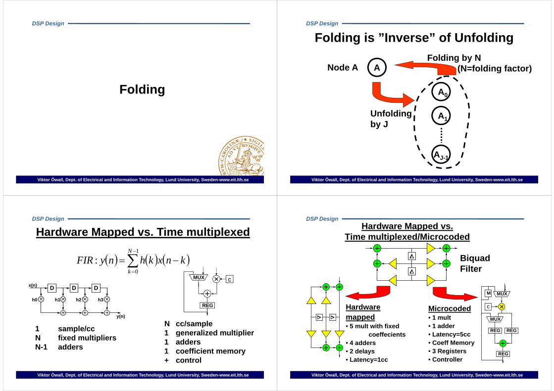
So why didn’t the filter look like this?(S |3) (S |1)(S1|3) (S1|1)
In Out1 2
a(S1|2) (S1|0)
bD1 23 45 6
c d
(S1|2) ( 1| )(S2|0) (S2|2)
8Dc d
(S2|3) (S2|1)
7 8(S2|3) ( 2| )
Viktor Öwall, Dept. of Electrical and Information Technology, Lund University, Sweden-www.eit.lth.se
DSP Design
So why didn’t the filter look like this?(S |3) (S |1)(S1|3) (S1|1)
In Out1 2
a(S1|2) (S1|0)
bD1 23 45 6
c d
(S1|2) ( 1| )(S2|0) (S2|2)
8D1adderT 2multTc d
(S2|3) (S2|1)
7 81adder
adder
P 2mult
mult
P(S2|3) ( 2| )
1324S 7685SAdditions Multiplication
adder mult
Viktor Öwall, Dept. of Electrical and Information Technology, Lund University, Sweden-www.eit.lth.se
1,3,2,41 S 7,6,8,52 S
DSP Design
Folding of Biquad filter N=4Folding of Biquad filter, N=4sendreceive
DF(UV) = Nw(e) - Pu + v – u
DF(12) = -3(S1|3) (S1|1)
In OutF( )DF(15) = 0DF(16) = 2DF(17) = 7 a
In
bD1 23 45DF(17) 7
DF(18) = 5DF(31) = 0D (42) = 0
(S1|2) (S1|0)(S2|0) (S2|2)
b3 45 6DF(42) = 0DF(53) = 0DF(64) = -4D (73) = 3
c d( 2| ) ( 2| )
7 8D
DF(73) = -3DF(84) = -3
N t V lid f ldi0)( VUD(S2|3) (S2|1)
Viktor Öwall, Dept. of Electrical and Information Technology, Lund University, Sweden-www.eit.lth.se
Not Valid folding0)( VUDF
DSP Design
Folding of Biquad filter N=4Folding of Biquad filter, N=4
(S1|3) (S1|1)In Out
a
In
bD1 23 45
(S1|2) (S1|0)(S2|0) (S2|2)
b3 45 6
c d( 2| ) ( 2| )
7 8D Feedforward
cutset Retiming(S2|3) (S2|1)
cutset Pipelining
RetimingSplit and move delay
Viktor Öwall, Dept. of Electrical and Information Technology, Lund University, Sweden-www.eit.lth.se
move delay
DSP Design
F ldi f Bi d filtFolding of Biquad filter
(S1|3)D
(S1|1)In OutD
a
In Out
bD1 23 4
Da
(S1|2) (S1|0)(S2|0) (S2|2)
b3 45 6
DDD
c d( 2| ) (S2| )
7 8D(S2|3) (S2|1)
Viktor Öwall, Dept. of Electrical and Information Technology, Lund University, Sweden-www.eit.lth.se

DSP Design
Folding of Biquad filter, N=4(S |1)(S |3)
D(S1|1)
In Out1 2
(S1|3)
Da
(S1|2) (S1|0)bD
13 45 6
1adderT 2multTD
D
D c d
(S1|2) ( 1| )(S2|0) (S2|2)
7 81adder
adder
P 2mult
mult
PDc d
(S2|3) (S2|1)
7 8
1324S 7685SAdditions Multiplication
( 2| ) ( 2| )
Viktor Öwall, Dept. of Electrical and Information Technology, Lund University, Sweden-www.eit.lth.se
1,3,2,41 S 7,6,8,52 S
DSP Design
Folding of Biquad filter N=4Folding of Biquad filter, N=4sendreceive
DF(UV) = Nw(e) - Pu + v – u
D(S1|1)
In Out(S1|3)
DF(12) = 4(1) – 1 + 1 – 3 = 1DF(15) = 4(1) – 1 + 0 – 3 = 0DF(16) = 4(1) – 1 + 2 – 3 = 2
D
Da bD1 2
3 45 6DF(16) 4(1) 1 2 3 2DF(17) = 4(1) – 1 + 3 – 3 = 3DF(18) = 4(2) – 1 + 1 – 3 = 5D (31) = 4(0) 1 + 3 2 = 0 D
DD c d
(S1|2) (S1|0)(S2|0) (S2|2)
5 6
7DF(31) = 4(0) – 1 + 3 – 2 = 0DF(42) = 4(0) – 1 + 1 – 0 = 0DF(53) = 4(0) – 2 + 2 – 0 = 0D (6 4) 4(1) 2 + 0 2 0
DDD
c d
(S2|3) (S2|1)
7 8
DF(64) = 4(1) – 2 + 0 – 2 = 0DF(73) = 4(1) – 2 + 2 – 3 = 1DF(84) = 4(1) – 2 + 0 – 1 = 1
Valid folding0)( VUD
Viktor Öwall, Dept. of Electrical and Information Technology, Lund University, Sweden-www.eit.lth.se
0)( VUDF
DSP Design
Folding of Biquad filter N=4Folding of Biquad filter, N=4sendreceive 1adderP
DF(UV) = Nw(e) - Pu + v – u
D(S1|1)
In Out(S1|3)
1adderP
DF(12) = 4(1) – 1 + 1 – 3 = 1DF(15) = 4(1) – 1 + 0 – 3 = 0DF(16) = 4(1) – 1 + 2 – 3 = 2
D
Da bD1 2
3 45 6DF(16) 4(1) 1 2 3 2DF(17) = 4(1) – 1 + 3 – 3 = 3DF(18) = 4(2) – 1 + 1 – 3 = 5D (31) = 4(0) 1 + 3 2 = 0 D
DD c d
(S1|2) (S1|0)(S2|0) (S2|2)
5 6
7DF(31) = 4(0) – 1 + 3 – 2 = 0DF(42) = 4(0) – 1 + 1 – 0 = 0DF(53) = 4(0) – 2 + 2 – 0 = 0D (6 4) 4(1) 2 + 0 2 0
DDD
c d
(S2|3) (S2|1)
7 8
DF(64) = 4(1) – 2 + 0 – 2 = 0DF(73) = 4(1) – 2 + 2 – 3 = 1DF(84) = 4(1) – 2 + 0 – 1 = 1
Valid folding0)( VUD
Viktor Öwall, Dept. of Electrical and Information Technology, Lund University, Sweden-www.eit.lth.se
0)( VUDF
DSP Design
Folding of Biquad filter N=4Folding of Biquad filter, N=4
5 delays
1,3,2,41 SAdditions
7,6,8,52 SMultiplication
DF(18) = 4(2) – 1 + 1 – 3 = 5 path from add to mult with 5D
Viktor Öwall, Dept. of Electrical and Information Technology, Lund University, Sweden-www.eit.lth.se
Node 8 has folding order 1 switch close at 1

DSP Design
Folding of Biquad filterFolding of Biquad filter
1,3,2,41 SAdditions
7,6,8,52 SMultiplication
DF(31) = 4(0) – 1 + 3 – 2 = 0 path from add to add with 0DNode 1 has folding order 3 switch close at 3
Viktor Öwall, Dept. of Electrical and Information Technology, Lund University, Sweden-www.eit.lth.se
Node 1 is also connected to the input
DSP Design
Folding of Biquad filterFolding of Biquad filter
1,3,2,41 SAdditions
7,6,8,52 SMultiplication
Execution of node 2 (input from node 1 and 4) :Execution of node 2 (input from node 1 and 4) :DF(12) = 4(1) – 1 + 1 – 3 = 1 path from add to add with 1DNode 2 has folding order 1 switch close at 1
Viktor Öwall, Dept. of Electrical and Information Technology, Lund University, Sweden-www.eit.lth.se
gDF(4 2) = 4(0) – 1 + 1 – 0 = 0 path from add to add with 0D
DSP Design
Folding of Biquad filter N=4Folding of Biquad filter, N=4sendreceive
DF(UV) = Nw(e) - Pu + v – u
D(S1|1)
In Out(S1|3)
DF(12) = 4(1) – 1 + 1 – 3 = 1DF(15) = 4(1) – 1 + 0 – 3 = 0DF(16) = 4(1) – 1 + 2 – 3 = 2
D
Da bD1 2
3 45 6DF(16) 4(1) 1 2 3 2DF(17) = 4(2) – 1 + 3 – 3 = 7DF(18) = 4(2) – 1 + 1 – 3 = 5D (31) = 4(0) 1 + 3 2 = 0 D
Dc d
(S1|2) (S1|0)(S2|0) (S2|2)
5 6
7 DDDF(31) = 4(0) – 1 + 3 – 2 = 0DF(42) = 4(0) – 1 + 1 – 0 = 0DF(53) = 4(0) – 2 + 2 – 0 = 0D (6 4) 4(1) 2 + 0 2 0
Dc d
(S2|3) (S2|1)
7 8DD
DDF(64) = 4(1) – 2 + 0 – 2 = 0DF(73) = 4(0) – 2 + 2 – 3 = -3DF(84) = 4(1) – 2 + 0 – 1 = 1
Not valid folding0)( VUD
Viktor Öwall, Dept. of Electrical and Information Technology, Lund University, Sweden-www.eit.lth.se
0)( VUDF
DSP Design
H d M d Mi d dHardware Mapped vs. Microcoded
BiquadFilter
M MUX
Hardware d
c
M MUX
Microcodedmapped• 5 mult with fixed
coeffecientsREG
MUX
REG
• 1 mult• 1 adder• Latency=5cccoeffecients
• 4 adders• 2 delays
L t 1REG
Latency 5cc• Coeff Memory• 3 Registers
C t ll
Viktor Öwall, Dept. of Electrical and Information Technology, Lund University, Sweden-www.eit.lth.se
• Latency=1cc • Controller

DSP Design
Retiming for Folding
U Vr(U) r(V)(e)
If D’F(UV) is the folded delays of theedge UV for the retimed graph then D’ (UV) 0 U Vr(U) r(V)
( )
D’F(UV) 0 Nwr(e) – PU + v – u 0
U Vr (e) N(w(e) + r(V) – r(U) ) - PU + v – u 0
r (e) = (e) + r(V) - r(U) N(r(U) – r(V)) Nw(e) - PU + v – u
r(U) – r(V) D (UV) /N
sendreceive
r(U) – r(V) DF(UV) /N
r(U) – r(V) DF(UV) /N
Viktor Öwall, Dept. of Electrical and Information Technology, Lund University, Sweden-www.eit.lth.se
( ) ( ) F( )(floor since retiming values are integers)
DSP Design
Register/Storage MinimizationF ldi i t i t Lif ti l i i d f i tFolding inserts register. Lifetime analysis is used for register minimization techniques in a DSP hardware.
• A variable is live from the time it is produced until the time it is consumed. After that it is deadAfter that it is dead.
• Linear lifetime chart : Represents the lifetime of the variables in a linear fashion.
• Convention: a variable is
• not live during the clock cycle when• not live during the clock cycle when it is produced
• but live during the clock cycle when
Viktor Öwall, Dept. of Electrical and Information Technology, Lund University, Sweden-www.eit.lth.se
but live during the clock cycle when it is consumed. One iteratiom 6 cc N=6
DSP Design
R i t Mi i i tiRegister MinimizationMax. number of live variables Min. number of registersg
Use previous iterUse previous iter.to avoid drawinglifetime chart overseveral iterationsseveral iterations
2 livevariables
But 3 if several iterations
Viktor Öwall, Dept. of Electrical and Information Technology, Lund University, Sweden-www.eit.lth.se
2 live variables in iteration
DSP Design
R i t Mi i i tiRegister MinimizationMax. number of live variables Min. number of registersg
6cc66cc6cc
2 livevariables
But 3 if several iterations
Viktor Öwall, Dept. of Electrical and Information Technology, Lund University, Sweden-www.eit.lth.se
2 live variables in iteration

DSP Design
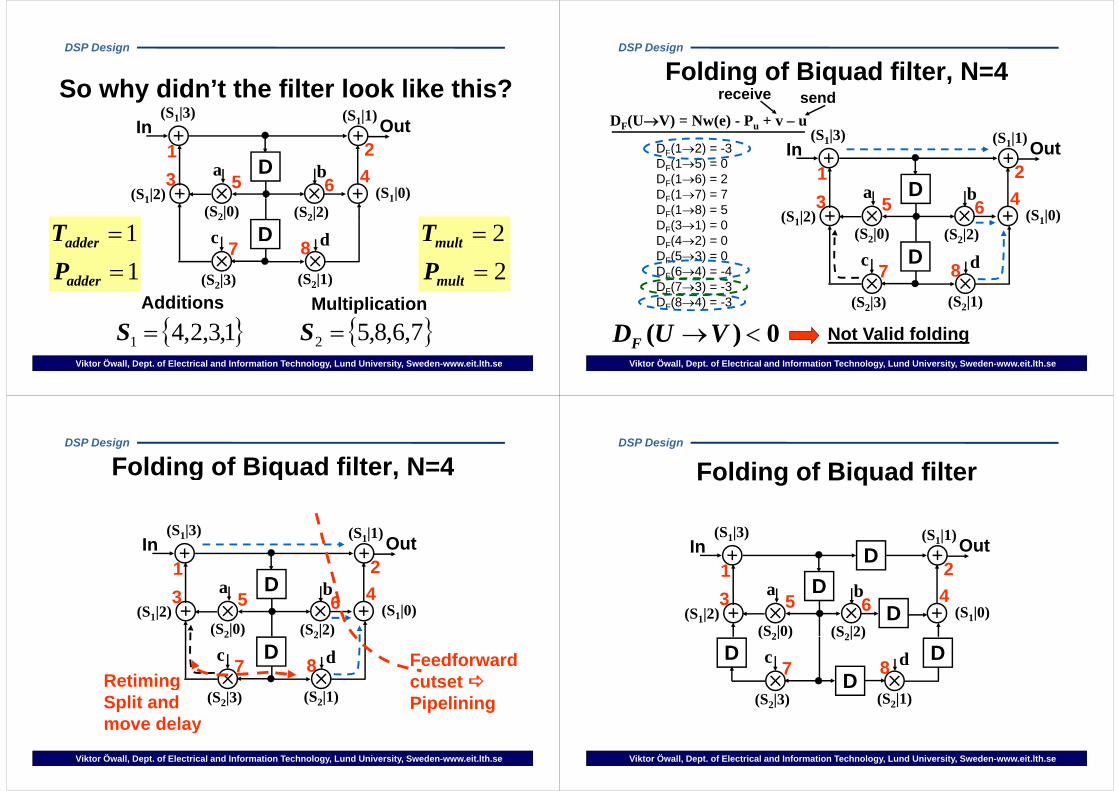
3x3 Matrix Transpose
fdcba
hbgda
ihgfed
ifcheb
ihg ifc
Matrix Transposer
i | h | g | f | e | d | c | b | a i | f | c | h | e | b | g | d | a
One iteration = 9 clock cycles
Viktor Öwall, Dept. of Electrical and Information Technology, Lund University, Sweden-www.eit.lth.se
y
DSP Design
Lifetime Table 3x3 Matrix TransposeLifetime Table - 3x3 Matrix TransposeMatrix i | h | g | f | e | d | c | b | a i | f | c | h | e | b | g | d | aMatr x
Transposer
Sample Tin Tzlout Tdiff Tout Lifea 0 0b 1 3
2 6Out before Inc 2 6d 3 1e 4 4
Out before In-2
e 4 4f 5 7g 6 2h 7 5i 8 8
Viktor Öwall, Dept. of Electrical and Information Technology, Lund University, Sweden-www.eit.lth.se
DSP Design
Lifetime Table 3x3 Matrix TransposeLifetime Table - 3x3 Matrix TransposeMatrix i | h | g | f | e | d | c | b | a i | f | c | h | e | b | g | d | aMatr x
Transposer
Sample Tin Tzlout Tdiff Tout Lifea 0 0 0b 1 3 2
2 6 4c 2 6 4d 3 1 -2e 4 4 0e 4 4 0f 5 7 2g 6 2 -4h 7 5 -2i 8 8 0
Viktor Öwall, Dept. of Electrical and Information Technology, Lund University, Sweden-www.eit.lth.se
Tdiff = Tzlout – Tinput, Tzlout = zero latency
DSP Design
3x3 Matrix TransposeSample Ti T l Tdiff T Life
3x3 Matrix TransposeSample Tin Tzlout Tdiff Tout Life
a 0 0 0b 1 3 2c 2 6 4d 3 1 -2 5e 4 4 0f 5 7 2g 6 2 -4g 6 2 4h 7 5 -2i 8 8 0
if Tdiff < 0 not causal add latency = | T | for all nodes
Viktor Öwall, Dept. of Electrical and Information Technology, Lund University, Sweden-www.eit.lth.se
add latency = | Tnegative diffmax| for all nodes

DSP Design
3x3 Matrix TransposeSample Ti T l Tdiff T Life
3x3 Matrix TransposeSample Tin Tzlout Tdiff Tout Life
a 0 0 0 4 04b 1 3 2 7 17c 2 6 4 10 210d 3 1 -2 5 35e 4 4 0 8 48f 5 7 2 11 511g 6 2 -4 6 66g 6 2 4 6 66h 7 5 -2 9 79i 8 8 0 12 812
if Tdiff < 0 not causal add latency = | T | for all nodes
Viktor Öwall, Dept. of Electrical and Information Technology, Lund University, Sweden-www.eit.lth.se
add latency = | Tnegative diffmax| for all nodes
DSP Design
Lifetime chart 3x3 Matrix TransposeLifetime chart 3x3 Matrix TransposeSampl Ti T l Tdiff T LifeSampl
eTin Tzlout Tdiff Tout Life
a 0 0 0 4 04
cycle01
a b c d e f g h i #live01
b 1 3 2 7 17c 2 6 4 10 210d 3 1 2 5 35
2345
2344d 3 1 -2 5 35
e 4 4 0 8 48f 5 7 2 11 511
5678
4444
g 6 2 -4 6 66h 7 5 -2 9 79
9101112
4321
+0+1+2+3i 8 8 0 12 812 12 1
One iteration =
+3
Contribution from next
Viktor Öwall, Dept. of Electrical and Information Technology, Lund University, Sweden-www.eit.lth.se
9 clock cycleso e t
iteration
DSP Design
Lifetime chart 3x3 Matrix TransposeLifetime chart 3x3 Matrix TransposeSampl Ti T l Tdiff T LifeSampl
eTin Tzlout Tdiff Tout Life
a 0 0 0 4 04
cycle01
a b c d e f g h i #live01
b 1 3 2 7 17c 2 6 4 10 210d 3 1 2 5 35
2345
2344d 3 1 -2 5 35
e 4 4 0 8 48f 5 7 2 11 511
5678
4444
g 6 2 -4 6 66h 7 5 -2 9 79
9101112
4321
+0=4+1=4+2=4+3=4i 8 8 0 12 812 12 1
One iteration = The total
+3=4
Viktor Öwall, Dept. of Electrical and Information Technology, Lund University, Sweden-www.eit.lth.se
9 clock cycles
DSP Design
Lifetime chartLifetime chartOne iteration = 9 clock cycles
# #cycle012
a b c d e f g h i #live012
cycle012
a b c d e f g h i #live0122
3456
23444
23456
234446
789
4444 +0
6789
44449
101112
4321
0+1+2+3
910111213
44444
Contribution from next it ti
13141516
4444
Viktor Öwall, Dept. of Electrical and Information Technology, Lund University, Sweden-www.eit.lth.se
iteration 161718
444
DSP Design
Lifetime chart 3x3 Matrix TransposeLifetime chart 3x3 Matrix TransposeSampl Ti T l Tdiff T LifeSampl
eTin Tzlout Tdiff Tout Life
a 0 0 0 4 04b 1 3 2 7 17c 2 6 4 10 210d 3 1 2 5 35 x x x xd 3 1 -2 5 35e 4 4 0 8 48f 5 7 2 11 511
x x x x
g 6 2 -4 6 66h 7 5 -2 9 79
#lii 8 8 0 12 812 max #live =4 registers
Viktor Öwall, Dept. of Electrical and Information Technology, Lund University, Sweden-www.eit.lth.se
DSP Design
Circular lifetime chart
Useful to represent the periodic naturethe periodic nature of the DSP programs.
Viktor Öwall, Dept. of Electrical and Information Technology, Lund University, Sweden-www.eit.lth.se
DSP Design
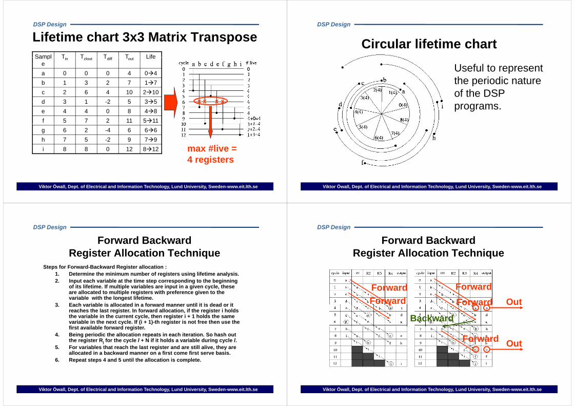
F d B k dForward Backward Register Allocation Technique
Steps for Forward-Backward Register allocation :1. Determine the minimum number of registers using lifetime analysis.2. Input each variable at the time step corresponding to the beginning2. Input each variable at the time step corresponding to the beginning
of its lifetime. If multiple variables are input in a given cycle, these are allocated to multiple registers with preference given to the variable with the longest lifetime.
3 Each variable is allocated in a forward manner until it is dead or it3. Each variable is allocated in a forward manner until it is dead or it reaches the last register. In forward allocation, if the register i holds the variable in the current cycle, then register i + 1 holds the same variable in the next cycle. If (i + 1)-th register is not free then use the first available forward registerfirst available forward register.
4. Being periodic the allocation repeats in each iteration. So hash out the register Rj for the cycle l + N if it holds a variable during cycle l.
5. For variables that reach the last register and are still alive, they are5. For variables that reach the last register and are still alive, they are allocated in a backward manner on a first come first serve basis.
6. Repeat steps 4 and 5 until the allocation is complete.
Viktor Öwall, Dept. of Electrical and Information Technology, Lund University, Sweden-www.eit.lth.se
DSP Design
F d B k dForward Backward Register Allocation Technique
ForwardForwardForwardForward Out
Backward
Forward Out
Forward Out
Viktor Öwall, Dept. of Electrical and Information Technology, Lund University, Sweden-www.eit.lth.se

DSP Design
Folded Architecture forFolded Architecture for Matrix Transposerp
4 Registers
Viktor Öwall, Dept. of Electrical and Information Technology, Lund University, Sweden-www.eit.lth.se
DSP Design
Controller for Folded Architecture
Controllerfor Switches
Viktor Öwall, Dept. of Electrical and Information Technology, Lund University, Sweden-www.eit.lth.se
for Switches
DSP Design
First-In-First-Out, FIFO
Moving data consumes power
RE
RE
RE
RE
RE
REE
GEG
EG
EG
EG
EG
Latency since data has to move ythrough all registers
Viktor Öwall, Dept. of Electrical and Information Technology, Lund University, Sweden-www.eit.lth.se
DSP Design
FIFO, continued
Connecting outputs to remove latency and remove data shifts
RE
RE
RE
RE
RE
RE
latency and remove data shifts
EG
EG
EG
EG
EG
EG
ControllerController
Controllerto choose
outputViktor Öwall, Dept. of Electrical and Information Technology, Lund University, Sweden-www.eit.lth.se
output

DSP Design
FIFO, continuedConnecting inputsConnecting inputs.What do we have?
RAMRE
RE
RE
RE
RE
RE
a RAM
EG
EG
EG
EG
EG
EG
Addresscalculation
Viktor Öwall, Dept. of Electrical and Information Technology, Lund University, Sweden-www.eit.lth.se
calculation
DSP Design
FIFO with pointers
OUT
RAMAddress(pointer)RAM
IN
calculation
IN
No moving of databut complexity in address calculation
Viktor Öwall, Dept. of Electrical and Information Technology, Lund University, Sweden-www.eit.lth.se
but complexity in address calculation
DSP Design
Lifetime chart 3x3 Matrix TransposeLifetime chart 3x3 Matrix Transpose
4 registersPossible to
use memoryuse memory with
4 positions
Viktor Öwall, Dept. of Electrical and Information Technology, Lund University, Sweden-www.eit.lth.se
4 positions
DSP Design
R i t Mi i i ti f Bi d filtRegister Minimization of Biquad filter
0
One entry for each node:• Tinput = u + Pu, u=folding order, Pu=pipeline
time unit data is produced
•T t t = u + P + maxV{DF(U V)},
Viktor Öwall, Dept. of Electrical and Information Technology, Lund University, Sweden-www.eit.lth.se
Toutput u + Pu + maxV{DF(U V)},maxV{DF(U V)} = (longest folded path)

DSP Design
R i t Mi i i ti f Bi d filtDF(UV) = Nw(e) - Pu + v – uRegister Minimization of Biquad filter
sendu
DF(12) = 1DF(15) = 0DF(16) = 2
receiveF( )
DF(17) = 3DF(18) = 5DF(31) = 0
node 1 2,5,6,7,8
0DF(31) 0DF(42) = 0DF(53) = 0D (64) = 0DF(64) = 0DF(73) = 1DF(84) = 1
One entry for each node:• Tinput = u + Pu = 3 + 1 = 4
Viktor Öwall, Dept. of Electrical and Information Technology, Lund University, Sweden-www.eit.lth.se
•Toutput = u + Pu + maxV{DF(U V)} = 3 + 1 + maxV{1,0,2,3,5} = 9
DSP Design
Register Minimi ation of Biq ad filterNode TinTout
Register Minimization of Biquad filter
1 492 --DF(12) = 13 2+1=3
2+1+0=34 4+1=5
DF(15) = 0DF(16) = 2DF(17) = 3 4 4 1 5
4+1+0=55 0+2=2
0+2=2
FDF(18) = 5DF(31) = 0DF(42) = 0
0
6 2+2=42+2=4
7 3+2=5
F( )DF(53) = 0DF(64) = 0DF(73) = 1 7 3+2=5
3+2+1=68 1+2=3
1+2+1=4
DF(73) = 1DF(84) = 1 One entry for each node:
• Tinput = u + Pu
Viktor Öwall, Dept. of Electrical and Information Technology, Lund University, Sweden-www.eit.lth.se
1 2 1 4
•Toutput = u + Pu + maxV{DF(U V)}
DSP Design
Lifetime chart of Biquad filterLifetime chart of Biquad filter...
Node TinTout
1 491 t it
2 --3 334 11
1st iter.
4 115 226 44
2nd iter.
7 568 34 3rd iter.
Viktor Öwall, Dept. of Electrical and Information Technology, Lund University, Sweden-www.eit.lth.se
DSP Design
and Register Allocation...and Register Allocation
1st iter.
2nd iter.
3rd iter.
Viktor Öwall, Dept. of Electrical and Information Technology, Lund University, Sweden-www.eit.lth.se

DSP Design
F ld d hit t i dFolded architecture is drawn with minimum # of registers.with minimum # of registers.
Viktor Öwall, Dept. of Electrical and Information Technology, Lund University, Sweden-www.eit.lth.se
DSP Design
Previous architecture
Viktor Öwall, Dept. of Electrical and Information Technology, Lund University, Sweden-www.eit.lth.se
DSP Design
Bi d FiltBiquad FilterImplementation using registers 1 sectionImplementation using registers, 1 section
M MUX
cMUX
REG REG
REG
Implementation using memoriesUsed for a speech scramblerwith 8 x 3 section biquads
Viktor Öwall, Dept. of Electrical and Information Technology, Lund University, Sweden-www.eit.lth.se
with 8 x 3 section biquads.
DSP Design
Which approach to use?D dDepends on:
• number of positionsb f• number of moves
• complexity of address calculationt• etc...
As the number of positionsAs the number of positions increase a memory solution becomes more favorablebecomes more favorable.
Decide on case by case basis.
Viktor Öwall, Dept. of Electrical and Information Technology, Lund University, Sweden-www.eit.lth.se
Decide on case by case basis.