dsp based current controlled single stage single phase ... · an integration criterion in switched...
TRANSCRIPT

Subbarao et al., Cogent Engineering (2017), 4: 1311460http://dx.doi.org/10.1080/23311916.2017.1311460
ELECTRICAL & ELECTRONIC ENGINEERING | RESEARCH ARTICLE
DSP based current controlled single stage single phase integrated converter with external compensating signal for Class-C & Class-D appliancesMopidevi Subbarao1*, Ch. Sai Babu2 and S. Satyanarayana3
Abstract: Design and implementation of a current controlled single stage sin-gle phase integrated AC/DC isolated Power Factor Correction (PFC) converter is presented in this paper. With the integrated topology reduces the number control switches. The proposed converter has the advantage of low bulk capacitor volt-age and only single control switch hence reduce in complexity in control and cost. Sub-harmonic oscillations which are produced in conventional current controller. By adding an external compensating signal effect of oscillations are reduced and performance of the converter is improved. The proposed scheme is implemented in real time by TMS320F2812 digital signal processor (DSP) board. The performance of converter is verified both experimentally and by simulation at different load and line conditions. The proposed converter is designed for 90–230 V, 50 Hz AC input, 48 V DC output and operating at 100 kHz switching frequency. The Experimental results shows that the DSP-based fuzzy controlled single phase single switch integrated PFC converter achieve high power factor and satisfies IEC-61000-3-2 and other European input current harmonic limits for Class-C & Class-D applications.
Subjects: Power & Energy; Electrical & Electronic Engineering; Digital Signal Processing; Electronics
Keywords: DSP; integrated converter; current control; IEC-61000-3-2; PFC
*Corresponding author: Mopidevi Subbarao, Department of EEE, VFSTR University, Vadlamudi, India E-mail: [email protected]
Reviewing editor:Qingsong Ai, Wuhan University of Technology, China
Additional information is available at the end of the article
ABOUT THE AUTHORSMopidevi Subbarao received BTech from JNTUH in 2000, MTech from JNTUA in 2007. He is currently pursuing the PhD degree at JNTU college of Engineering, Kakinada. His research interests include Power Electronics and Drives.
Ch. Sai Babu obtained PhD degree in Reliability Studies of HVDC Converters from JNTU, Hyderabad. Currently he is working as a Professor in Department of EEE in University College of Engineering, JNT University, Kakinada. His areas of interest are Power Electronics and Drives, Power System Reliability, HVDC Converter.
S. Satyanarayana, obtained PhD degree in Distribution Automation from JNTU college of Engineering, Hyderabad. Currently he is working as a Principal in Raghu Institute of Technology, Visakhapatnam. His research interests include Distribution Automation and Power Systems.
PUBLIC INTEREST STATEMENTAn integrated converter is a synthesized device based on the overall system integration, which is simplified by the system objective and can implement the system functions similar to the discrete converters without integration. Simplification means the process of synthesizing converters with reduced components, smaller size, and lower weight or cost. System objectives can include minimum cost, maximum efficiency, high reliability, low power packing, wide conversion range, PFC and output regulation, inverter PFC, and better performance.
In this paper 1-pahse integrated buck-flyback converter (IBFC) is analyzed, designed and implemented for Class-C & Class-D appliances. Experimental results of the proposed converter satisfy the IEC-61000-3-2 and other European standards.
Received: 04 November 2016Accepted: 23 March 2017First Published: 28 March 2017
© 2017 The Author(s). This open access article is distributed under a Creative Commons Attribution (CC-BY) 4.0 license.
Page 1 of 13
Mopidevi Subbarao

Page 2 of 13
Subbarao et al., Cogent Engineering (2017), 4: 1311460http://dx.doi.org/10.1080/23311916.2017.1311460
1. IntroductionBased on the current harmonic limits by IEC-61000-3-2 and other European standards, electrical equipment are classified into four groups: Class-A, Class-B, Class-C and Class-D (Table 1).
At present many works have been developed in order to comply with IEC-61000-3-2 power supply to above groups is through power electronic converters. In literature two techniques are proposed to comply these regulations (Basu & Bollen, 2005; Huber, Zhang, Jovanovic′, & Lee, 2001; Lu, Iu, & Pjevalica, 2008; Singh, Singh, Chandra, Al-Haddad, & Pandey, 2003).
(1) Using passive elements like inductor, capacitor along with uncontrolled rectifiers. It is a good solution only for low power ratings and difficult to operate in universal range of input due to the large size of passive elements (Singh et al., 2003).
(2) Other technique uses active power factor correction (PFC) circuit which consists of switching converter along with small size filter components. This technique reaches high efficiency and high power factor. Despite its expensiveness, complexity and EMI generation, this topology is considered as the best solution for high power levels and operating in universal range of input.
Active PFC techniques are of two types- single stage and two stage. Single stage topologies are boost, buck-boost or flyback converter. Major drawbacks with this topology are poor dynamic re-sponse and high switching stress (Basu & Bollen, 2005; Lu et al., 2008).
In two stage topology, first stage employees either buck or boost converter as a Power factor cor-rection (PFC) and second stage consists of buck-boost derived topologies or flyback converter for power conditioning (PC). Though this topology gives unit power factor and fast dynamic response has drawback of high component size and cost.
An alternate solution to meet the IEC-61000-3-2 standards for Class-C & Class-D equipment is integrated single stage converter. This is formed by integration of PFC stage and PC stage. In this, single control switch shares the two stages. This converter performance is same as two stage topol-ogy with reduced component size and cost. There are different integrated topologies presented in literature (Alonso, Calleja, Ribas, Corominas, & Rico- Secades, 2004; Dalla Costa, Alonso, Marchesan, Cervi, & Prado, 2007; Dalla Costa et al., 2010). This paper focuses on integrated buck flyback con-verter (IBFC) as a power factor corrected converter. In IBFC, buck converter for PFC and flyback converter feeds supply to the load, both converters are operating in DCM to achieve high power factor.
Analog PFC control used to be the general commercial control for Class-C & Class-D equipment. Due to advantages like insensitive to parameter variations, more reliable, less number of passive components, now a days, digital control has become a competitive option. Digital control can be implemented using low cost microprocessor or Digital signal processor (DSP) or Field programmable gate array (FPGA). In literature, several analog and digital control approaches have been proposed to improve power factor and achieve regulated voltage (Buccella, Cecati, & Latafat, 2012; Gegner & Lee, 1996; Jiuming & Shulin, 2011; Murahari Rao, Kumar Jain, Reddy, & Behal, 2008; Yang et al., 2015; Ye & Jovanovich, 2005; Zhang & Feng, 2006).
Table 1. Classification of electrical equipmentClass Equipment (Example)Class A Household appliances
Class B Non-professional arc welding equipment
Class C Lighting equipment
Class D Personal computers
Page 3 of 13
Subbarao et al., Cogent Engineering (2017), 4: 1311460http://dx.doi.org/10.1080/23311916.2017.1311460
In this paper, analysis and design of DSP (TMS320F2812) based Constant frequency Current Controlled Integrated buck flyback Converter with External ramp is implemented for Class-D & Class-C appliances to achieve high power factor and regulated voltage.
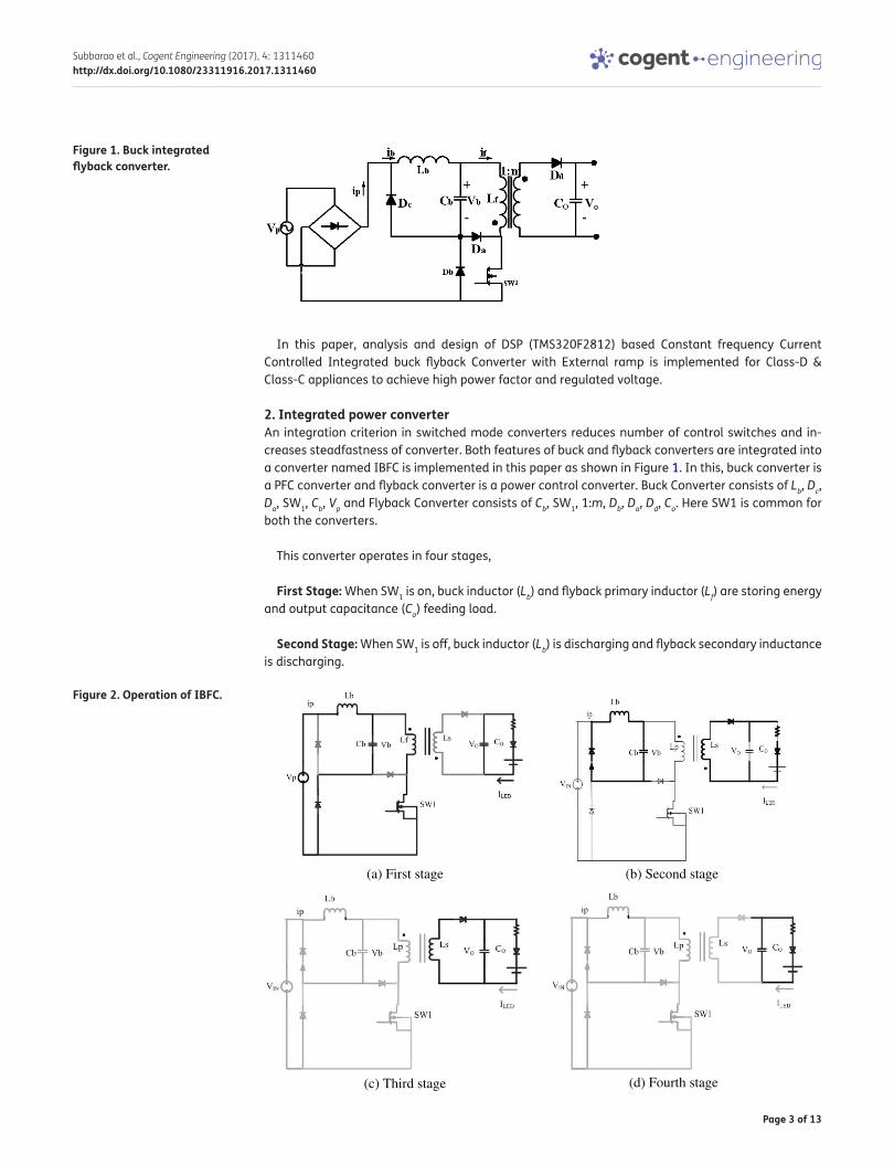
2. Integrated power converterAn integration criterion in switched mode converters reduces number of control switches and in-creases steadfastness of converter. Both features of buck and flyback converters are integrated into a converter named IBFC is implemented in this paper as shown in Figure 1. In this, buck converter is a PFC converter and flyback converter is a power control converter. Buck Converter consists of Lb, Dc, Da, SW1, Cb, Vp and Flyback Converter consists of Cb, SW1, 1:m, Db, Da, Dd, Co. Here SW1 is common for both the converters.
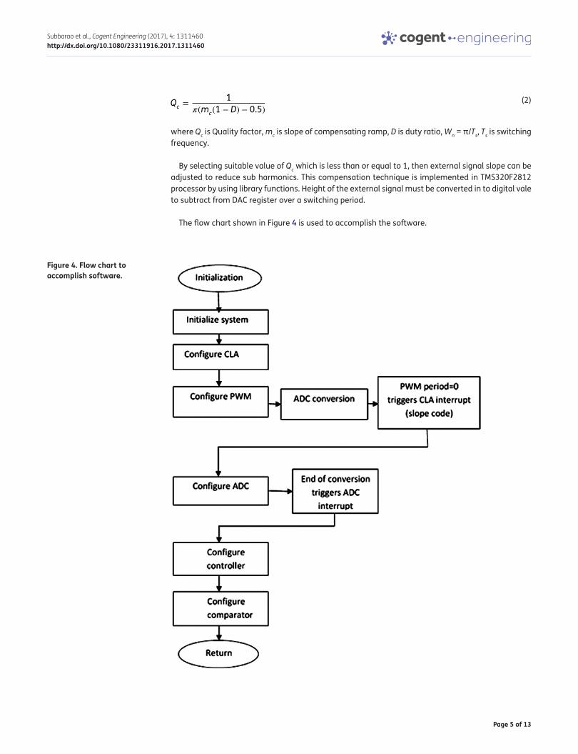
This converter operates in four stages,
First Stage: When SW1 is on, buck inductor (Lb) and flyback primary inductor (Lf) are storing energy and output capacitance (Co) feeding load.
Second Stage: When SW1 is off, buck inductor (Lb) is discharging and flyback secondary inductance is discharging.
Figure 2. Operation of IBFC.
(a) First stage
(c) Third stage
(b) Second stage
(d) Fourth stage
Figure 1. Buck integrated flyback converter.

Page 4 of 13
Subbarao et al., Cogent Engineering (2017), 4: 1311460http://dx.doi.org/10.1080/23311916.2017.1311460
Third Stage: Even before complete discharge of flyback secondary inductor energy, buck inductor discharges its energy completely.
Fourth Stage: In this, flyback secondary inductor discharges energy completely and output ca-pacitor feeds load.
The above four stages of working are shown in Figure 2.
3. Digital current control with slope compensationDue to high computational speed, high reliability and cost reduction now a day’s DSPs have been using extensively in various applications like control of drives, communication systems, intelligent systems etc. Figure 3 shows the block diagram of current controlled IBFC with external ramp by us-ing DSP (TMS320F2812). This control approach contains two loops an inner current loop to achieve near unity power factor and outer voltage loop to achieve regulated voltage. The control to output transfer function without external signal has high frequency term, due to this sub harmonics will occur, so in inner loop a compensating signal is added to reduce sub harmonic oscillations. Control to output transfer function is,
(1)H(S) =1
1 + S
WnQC+
S2
W2n
Figure 3. Block diagram of current controlled IBFC with external ramp by using DSP.
Page 5 of 13
Subbarao et al., Cogent Engineering (2017), 4: 1311460http://dx.doi.org/10.1080/23311916.2017.1311460
where Qc is Quality factor, mc is slope of compensating ramp, D is duty ratio, Wn = π/Ts, Ts is switching frequency.
By selecting suitable value of Qc which is less than or equal to 1, then external signal slope can be adjusted to reduce sub harmonics. This compensation technique is implemented in TMS320F2812 processor by using library functions. Height of the external signal must be converted in to digital vale to subtract from DAC register over a switching period.
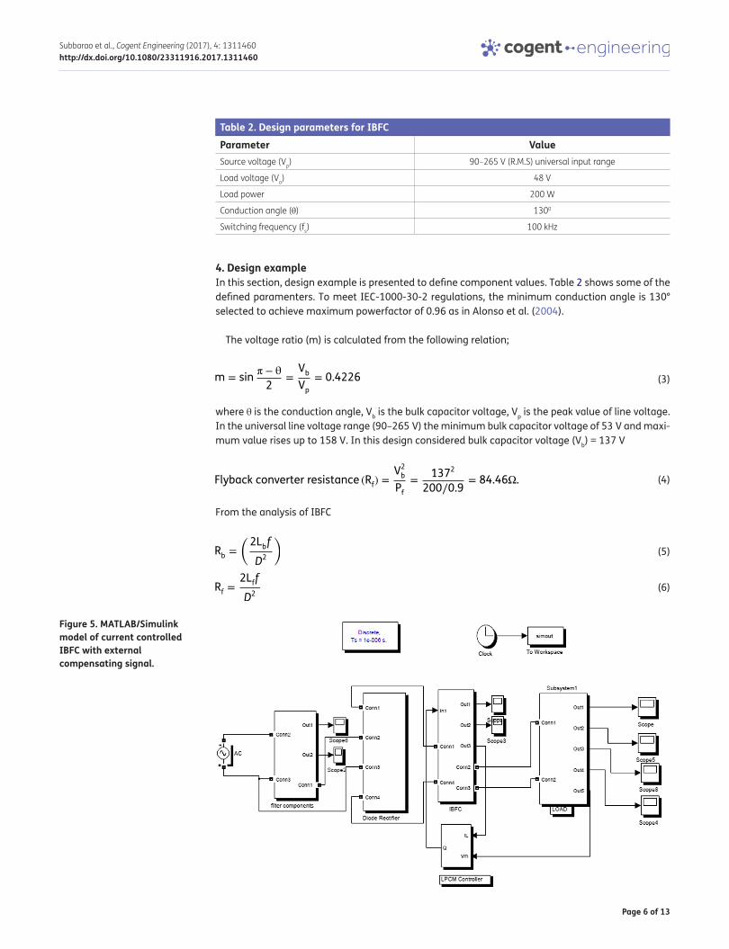
The flow chart shown in Figure 4 is used to accomplish the software.
(2)Qc =1
�(mc(1 − D) − 0.5)
Figure 4. Flow chart to accomplish software.
Page 6 of 13
Subbarao et al., Cogent Engineering (2017), 4: 1311460http://dx.doi.org/10.1080/23311916.2017.1311460
4. Design exampleIn this section, design example is presented to define component values. Table 2 shows some of the defined paramenters. To meet IEC-1000-30-2 regulations, the minimum conduction angle is 130° selected to achieve maximum powerfactor of 0.96 as in Alonso et al. (2004).
The voltage ratio (m) is calculated from the following relation;
where θ is the conduction angle, Vb is the bulk capacitor voltage, Vp is the peak value of line voltage. In the universal line voltage range (90–265 V) the minimum bulk capacitor voltage of 53 V and maxi-mum value rises up to 158 V. In this design considered bulk capacitor voltage (Vb) = 137 V
From the analysis of IBFC
(3)m = sinπ − θ
2=VbVp
= 0.4226
(4)Flyback converter resistance (Rf) =V2bPf
=1372
200∕0.9= 84.46Ω.
(5)Rb =
(
2Lbf
D2
)
(6)Rf =2Lff
D2
Figure 5. MATLAB/Simulink model of current controlled IBFC with external compensating signal.
Table 2. Design parameters for IBFCParameter ValueSource voltage (Vp) 90–265 V (R.M.S) universal input range
Load voltage (Vo) 48 V
Load power 200 W
Conduction angle (θ) 1300
Switching frequency (fs) 100 kHz

Page 7 of 13
Subbarao et al., Cogent Engineering (2017), 4: 1311460http://dx.doi.org/10.1080/23311916.2017.1311460
Figure 6. Source voltage and current wave form for Vrms of 150 V.
Figure 7. Source voltage and current wave form for Vrms of 230 V.
Figure 8. Load voltage waveform without load change
Figure 9. Load current waveform without load change.
Page 8 of 13
Subbarao et al., Cogent Engineering (2017), 4: 1311460http://dx.doi.org/10.1080/23311916.2017.1311460
From (5) Lb = 178 μH and From (6) Lf = 754 μH.
Buck capacitor (Cb) = 220 μF.
5. Simulation and experimental results
5.1. Simulation resultsCurrent controlled integrated converter with external ramp compensation is implemented in MATLAB/Simulink. Figure 5 shows the simulink model of converter.
Figure 12. Voltage across the bulk capacitor before load change.
Figure 13. Voltage across the bulk capacitor after load change.
Figure 10. Load current waveform with step load change at 0.25 s from 4–2 A.
Figure 11. Load voltage waveform with load change at 0.25 s.
Page 9 of 13
Subbarao et al., Cogent Engineering (2017), 4: 1311460http://dx.doi.org/10.1080/23311916.2017.1311460
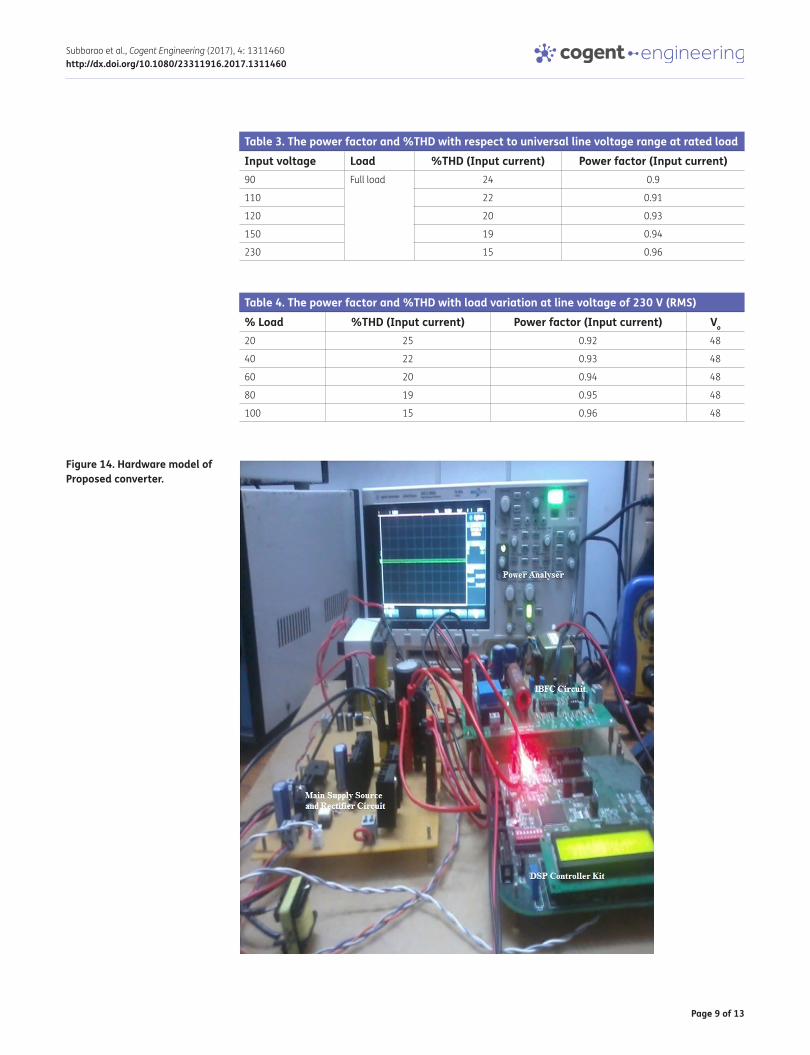
Figure 14. Hardware model of Proposed converter.
Table 3. The power factor and %THD with respect to universal line voltage range at rated loadInput voltage Load %THD (Input current) Power factor (Input current)90 Full load 24 0.9
110 22 0.91
120 20 0.93
150 19 0.94
230 15 0.96
Table 4. The power factor and %THD with load variation at line voltage of 230 V (RMS)% Load %THD (Input current) Power factor (Input current) Vo
20 25 0.92 48
40 22 0.93 48
60 20 0.94 48
80 19 0.95 48
100 15 0.96 48
Page 10 of 13
Subbarao et al., Cogent Engineering (2017), 4: 1311460http://dx.doi.org/10.1080/23311916.2017.1311460
Designed converter performance is verified for universal line voltage range at different load condi-tions. Figure 6 shows the source voltage and source current waveform for source voltage of 150 V at rated load, it is observed that source voltage and currents are in phase. The calculated power factor is 0.94 and respective line current %THD is 19%.
Converter is supplied with 230 V at rated load the corresponding line voltage & line current wave-form is shown in Figure 7. The power factor and line current %THD are 0.96 and 15%.
The Load voltage and load current wave forms are shown in Figures 8 and 9. It is observed that regulated load voltage of 48 V is appeared across the load and load current of 4A.
Load change is done on the converter at 0.2sec from rated load of 200–100 W the converter giving the regulated voltage of 48 V across the load terminals. This shows that converter operating effec-tively for load changes Figures 10 and 11 shows the respective load current and voltage waveforms of the converter with load change.
Figure 12 shows the bulk capacitor voltage is around 130 V, which is low voltage as compared to two stage and single stage converters. This is the special feature of integrated converter. Figure 13 shows the bulk capacitor voltage after load change at 0.25 s (Tables 3 and 4).
5.2. Experimental resultsDigital current controlled IBFC with external compensating signal is implemented experimentally by using TMS320F2812 DSP. Hardware setup was implemented in the laboratory as shown in the Figure 14 to investigate the performance of the controller for the integrated buck-flyback converter. The components used in the experimental work are tabulated in Table 5.
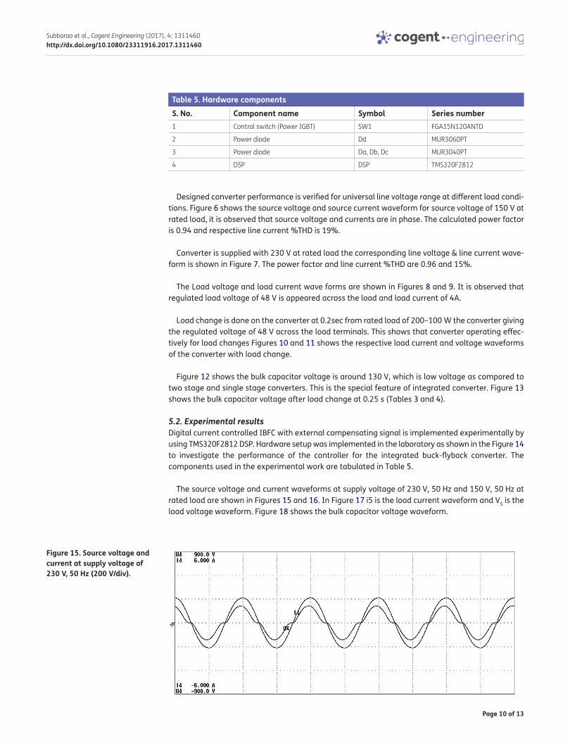
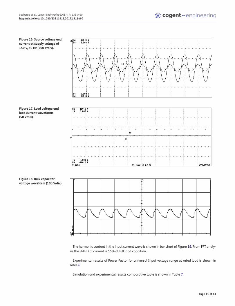
The source voltage and current waveforms at supply voltage of 230 V, 50 Hz and 150 V, 50 Hz at rated load are shown in Figures 15 and 16. In Figure 17 i5 is the load current waveform and V5 is the load voltage waveform. Figure 18 shows the bulk capacitor voltage waveform.
Figure 15. Source voltage and current at supply voltage of 230 V, 50 Hz (200 V/div).
Table 5. Hardware componentsS. No. Component name Symbol Series number1 Control switch (Power IGBT) SW1 FGA15N120ANTD
2 Power diode Dd MUR3060PT
3 Power diode Da, Db, Dc MUR3040PT
4 DSP DSP TMS320F2812
Page 11 of 13
Subbarao et al., Cogent Engineering (2017), 4: 1311460http://dx.doi.org/10.1080/23311916.2017.1311460
The harmonic content in the input current wave is shown in bar chart of Figure 19. From FFT analy-sis the %THD of current is 15% at full load condition.
Experimental results of Power Factor for universal Input voltage range at rated load is shown in Table 6.
Simulation and experimental results comparative table is shown in Table 7.
Figure 16. Source voltage and current at supply voltage of 150 V, 50 Hz (200 V/div).
Figure 17. Load voltage and load current waveforms (50 V/div).
Figure 18. Bulk capacitor voltage waveform (100 V/div).

Page 12 of 13
Subbarao et al., Cogent Engineering (2017), 4: 1311460http://dx.doi.org/10.1080/23311916.2017.1311460
6. ConclusionIntegrated power converter is designed by cascading buck converter with flyback converter because of having feature of current flowing through switch is either buck current or flyback current not sum of both currents, hence switch losses are reduced. Designed converter results are verified for differ-ent line and load conditions obtained lower value of power factor is 0.9 at low line voltage and reaches to 0.96 for 230 V, highest percentage of THD is 24% and lowest percentage of THD is 15% and it meets the IEC-6100-3-2 norms for Class-C & Class-D appliances. In the proposed current con-troller a digital compensating ramp signal is used for slope compensation to reduce sub-harmonics. This scheme applied to the converter and implemented in MATLAB/Simulink tool, their performance was evaluated both in steady state and dynamic conditions. Simulation and experimental results shows that controller acts quickly for load changes as shown in the load current waveform. Experimental results validate the satisfactory with simulation results.
Table 7. The comparative resultsSimulation results Experimental results
Input voltage 230 229
Output voltage 48 47.354
%THD 15 15.47
Power factor 0.96 0.957
Table 6. Experimental results for universal input voltage rangeInput voltage (V) 120 150 230 250
Power factor 0.93 0.94 0.957 0.943
Figure 19. THD bar graph for line current waveform.
FundingThe authors received no direct funding for this research.
Author detailsMopidevi Subbarao1
E-mail: [email protected] ID: http://orcid.org/0000-0002-5391-0978Ch. Sai Babu2
E-mail: [email protected]. Satyanarayana3
E-mail: [email protected] Department of EEE, VFSTR University, Vadlamudi, India.2 Department of EEE, College of Engineering JNTUK, Kakinada,
India.3 Raghu Institute of Technology, Visakhapatnam, India.
Citation informationCite this article as: DSP based current controlled single stage single phase integrated converter with external compensating signal for Class-C & Class-D appliances, Mopidevi Subbarao, Ch. Sai Babu & S. Satyanarayana, Cogent Engineering (2017), 4: 1311460.
ReferencesAlonso, J. M., Calleja, A. J., Ribas, J., Corominas, E. L., & Rico-
Secades, M. (2004, March). Analysis and design of a novel single-stage high-power- factor electronic ballast based on integrated buck half-bridge resonant inverter. IEEE Transactions on Power Electronics, 19, 550–559. http://dx.doi.org/10.1109/TPEL.2003.823246
Basu, S., & Bollen, M. H. J. (2005, July). A novel common power factor correction scheme for homes and offices. IEEE

Page 13 of 13
Subbarao et al., Cogent Engineering (2017), 4: 1311460http://dx.doi.org/10.1080/23311916.2017.1311460
© 2017 The Author(s). This open access article is distributed under a Creative Commons Attribution (CC-BY) 4.0 license.You are free to: Share — copy and redistribute the material in any medium or format Adapt — remix, transform, and build upon the material for any purpose, even commercially.The licensor cannot revoke these freedoms as long as you follow the license terms.
Under the following terms:Attribution — You must give appropriate credit, provide a link to the license, and indicate if changes were made. You may do so in any reasonable manner, but not in any way that suggests the licensor endorses you or your use. No additional restrictions You may not apply legal terms or technological measures that legally restrict others from doing anything the license permits.
Cogent Engineering (ISSN: 2331-1916) is published by Cogent OA, part of Taylor & Francis Group. Publishing with Cogent OA ensures:• Immediate, universal access to your article on publication• High visibility and discoverability via the Cogent OA website as well as Taylor & Francis Online• Download and citation statistics for your article• Rapid online publication• Input from, and dialog with, expert editors and editorial boards• Retention of full copyright of your article• Guaranteed legacy preservation of your article• Discounts and waivers for authors in developing regionsSubmit your manuscript to a Cogent OA journal at www.CogentOA.com
Transactions on Power Delivery, 20, 2257–2263. http://dx.doi.org/10.1109/TPWRD.2005.848444
Buccella, C., Cecati, C., & Latafat, H. (2012, August). Digital control of power converters—a survey. IEEE Transactions on Industrial Informatics, 8, 437–447. http://dx.doi.org/10.1109/TII.2012.2192280
Dalla Costa, M. A., Alonso, J. M., Marchesan, T. B., Cervi, M., & Prado, R. N. (2007, September). Generalized analysis and comparison of high-power-factor integrated topologies to supply metal halide lamps with low frequency square waveform (pp. 484–489). New Orleans, LA: Industry Applications Conference, 2007. 42nd IAS Annual Meeting. Conference Record of the 2007 IEEE.
Dalla Costa, M. A., Marchesan, T. B., da Silveira, J. S., Seidel, A. R., Nederson do Prado, R., & Alonso Alvarez, J. M. (2010, August). Integrated power topologies to supply HPS lamps: A comparative study. IEEE Transactions on Power Electronics, 25, 2124–2132. http://dx.doi.org/10.1109/TPEL.2010.2046183
Gegner, J. P., & Lee, C. Q. (1996). Linear peak current mode control: A simple active power factor correction control technique for continuous conduction mode (pp. 196–202). Power Electronics Specialists Conference, 1996.
Huber, L., Zhang, J., Jovanovic′, M. M., & Lee, F. C. (2001, July). Generalized topologies of single stage input-current-shaping circuits. IEEE Transactions on Power Electronics, 16, 98–107.
Jiuming, Z., & Shulin, L. (2011). Design of slope compensation circuit in peak current controlled mode converters (pp. 1310–1313). Electric Information and Control Engineering (ICEICE), 2011 International Conference.
Lu, D. D.-C., Iu, H. H.-C., & Pjevalica, V. (2008, March). A single-stage AC/DC converter with high power factor, regulated bus voltage, and output voltage. IEEE Transactions on Power Electronics, 23, 218–228.
Murahari Rao, V., Kumar Jain, A., Reddy, K. K., & Behal, A. (2008). Experimental comparison of digital implementations of single-phase PFC controllers. IEEE Transactions on Industrial Electronics, 55, 67–78.
Singh, B., Singh B. N., Chandra A., Al-Haddad K., & Pandey A. (2003). A review of single-phase improved power quality AC-DC converters. IEEE Transactions on Industrial Electronics, 50, 962–981. http://dx.doi.org/10.1109/TIE.2003.817609
Yang, C.-Y., Liu, Y.-c., Tseng, P.-J., Pan, T.-F., Chiu, H.-J., & Lo, Y.-K. (2015). DSP-based interleaved buck power factor corrector with adaptive slope compensation. IEEE Transactions on Industrial Electronics, 62, 4665–4677.
Ye, Z. Z., & Jovanovich, M. M. (2005, February). Implementation and performance evaluation of DSP-based control for constant-frequency discontinuous-conduction-mode boost PFC front end. IEEE Transactions on Industrial Electronics, 52, 98–107.
Zhang, W., & Feng, G. (2006, June). New digital control method for power factor correction‖. IEEE Transactions on Industrial Electronics, 53, 987–990.