dsi to hdmi adapter board for stm32 development tools€¦ · hdmi output port. it can be used on...
TRANSCRIPT
June 2016 DocID029197 Rev 1 1/12
1
UM2048User manual
DSI to HDMI adapter board for STM32 Development Tools
Introduction
The DSI to HDMI adapter board (order code B-LCDAD-HDMI1) provides DSI input port and HDMI output port. It can be used on STM32 evaluation boards or discovery boards, to demonstrate video solutions based on STM32 MCUs.
Thanks to the bridge chip ADV7533, the DSI to HDMI adapter board can support 2-, 3- or 4-lanes DSI video input data, S/PDIF, 2-channels I2S audio input data and HDMI v1.3 output port.
The B-LCDAD-HDMI1 adapter board has the following features:
• Up to four lanes of MIPI/DSI data, each running up to 800 Mbps (video mode only: Non-Burst mode with synchronization pulse)
• 2-channels I2S transmit stereo up to 192 kHz sampling rate
• S/PDIF carries stereo LPCM audio or compressed audio
• HDMI output connector:
– Support of video resolutions with pixel clocks up to 80 MHz
– Support of CEC signals, 5 V-tolerant I2C and HPD I/Os
– Common-mode filters with ESD protection
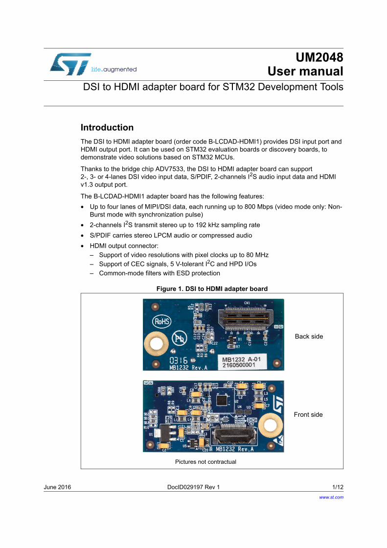
Figure 1. DSI to HDMI adapter board
Front side
Back side
Pictures not contractual
www.st.com

Contents UM2048
2/12 DocID029197 Rev 1
Contents
1 Hardware Layout and configuration . . . . . . . . . . . . . . . . . . . . . . . . . . . . 5
2 Video and audio input connector . . . . . . . . . . . . . . . . . . . . . . . . . . . . . . 6
2.1 Video input (MIPI DSI) signals . . . . . . . . . . . . . . . . . . . . . . . . . . . . . . . . . . 7
2.2 Audio input (S/PDIF & I2S) signals . . . . . . . . . . . . . . . . . . . . . . . . . . . . . . . 7
2.3 Control signals . . . . . . . . . . . . . . . . . . . . . . . . . . . . . . . . . . . . . . . . . . . . . . 7
3 HDMI output connector . . . . . . . . . . . . . . . . . . . . . . . . . . . . . . . . . . . . . . . 8
4 CEC . . . . . . . . . . . . . . . . . . . . . . . . . . . . . . . . . . . . . . . . . . . . . . . . . . . . . . . 9
5 Schematic . . . . . . . . . . . . . . . . . . . . . . . . . . . . . . . . . . . . . . . . . . . . . . . . 10
6 Revision history . . . . . . . . . . . . . . . . . . . . . . . . . . . . . . . . . . . . . . . . . . . 11
DocID029197 Rev 1 3/12
UM2048 List of tables
3
List of tables
Table 1. Video and audio input connector CN1 . . . . . . . . . . . . . . . . . . . . . . . . . . . . . . . . . . . . . . . . . 6Table 2. HDMI output connector CN2. . . . . . . . . . . . . . . . . . . . . . . . . . . . . . . . . . . . . . . . . . . . . . . . . 8Table 3. CEC source connection . . . . . . . . . . . . . . . . . . . . . . . . . . . . . . . . . . . . . . . . . . . . . . . . . . . . 9Table 4. Document revision history . . . . . . . . . . . . . . . . . . . . . . . . . . . . . . . . . . . . . . . . . . . . . . . . . 11
List of figures UM2048
4/12 DocID029197 Rev 1
List of figures
Figure 1. DSI to HDMI adapter board . . . . . . . . . . . . . . . . . . . . . . . . . . . . . . . . . . . . . . . . . . . . . . . . . 1Figure 2. Hardware Block Diagram . . . . . . . . . . . . . . . . . . . . . . . . . . . . . . . . . . . . . . . . . . . . . . . . . . . 5Figure 3. DSI to HDMI adapter board layout . . . . . . . . . . . . . . . . . . . . . . . . . . . . . . . . . . . . . . . . . . . . 5Figure 4. Board schematic . . . . . . . . . . . . . . . . . . . . . . . . . . . . . . . . . . . . . . . . . . . . . . . . . . . . . . . . . 10

DocID029197 Rev 1 5/12
UM2048 Hardware Layout and configuration
11
1 Hardware Layout and configuration
DSI to HDMI adapter board is designed around the ADV7533. Figure 2 illustrates the connections on DSI to HDMI adapter board and Figure 3 will help to locate these features on the actual evaluation board.
Figure 2. Hardware Block Diagram
Figure 3. DSI to HDMI adapter board layout
Video and audio input connector UM2048
6/12 DocID029197 Rev 1
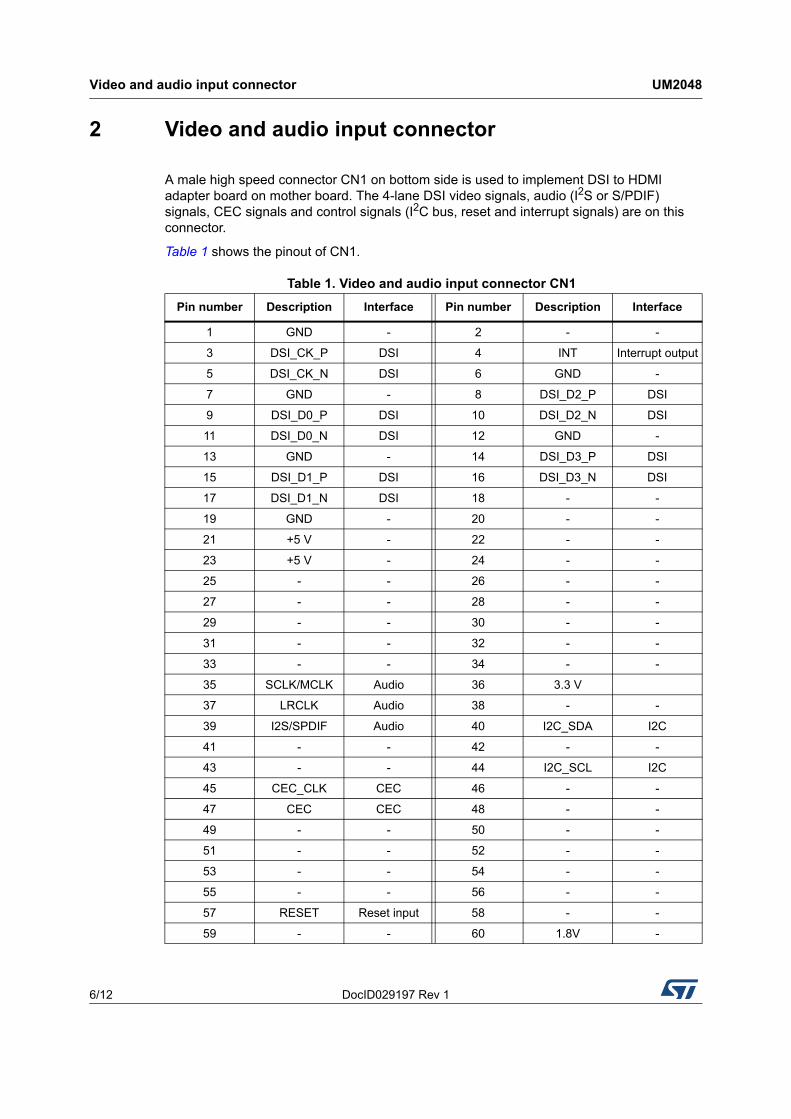
2 Video and audio input connector
A male high speed connector CN1 on bottom side is used to implement DSI to HDMI adapter board on mother board. The 4-lane DSI video signals, audio (I2S or S/PDIF) signals, CEC signals and control signals (I2C bus, reset and interrupt signals) are on this connector.
Table 1 shows the pinout of CN1.
Table 1. Video and audio input connector CN1
Pin number Description Interface Pin number Description Interface
1 GND - 2 - -
3 DSI_CK_P DSI 4 INT Interrupt output
5 DSI_CK_N DSI 6 GND -
7 GND - 8 DSI_D2_P DSI
9 DSI_D0_P DSI 10 DSI_D2_N DSI
11 DSI_D0_N DSI 12 GND -
13 GND - 14 DSI_D3_P DSI
15 DSI_D1_P DSI 16 DSI_D3_N DSI
17 DSI_D1_N DSI 18 - -
19 GND - 20 - -
21 +5 V - 22 - -
23 +5 V - 24 - -
25 - - 26 - -
27 - - 28 - -
29 - - 30 - -
31 - - 32 - -
33 - - 34 - -
35 SCLK/MCLK Audio 36 3.3 V
37 LRCLK Audio 38 - -
39 I2S/SPDIF Audio 40 I2C_SDA I2C
41 - - 42 - -
43 - - 44 I2C_SCL I2C
45 CEC_CLK CEC 46 - -
47 CEC CEC 48 - -
49 - - 50 - -
51 - - 52 - -
53 - - 54 - -
55 - - 56 - -
57 RESET Reset input 58 - -
59 - - 60 1.8V -

DocID029197 Rev 1 7/12
UM2048 Video and audio input connector
11
2.1 Video input (MIPI DSI) signals
4-lane MIPI DSI signals are connected on DSI to HDMI adapter board as video input interface. This board supports 2-, 3- or 4-lane DSI video input data and each running up to 800 Mbps.
DSI interface is compatible with DPHY V.0.90 and DSI V.1.02 and Supports inputs of 16-bit RGB 4:4:4, 24-bit RGB 4:4:4 and 30-bit RGB 4:4:4.
2.2 Audio input (S/PDIF & I2S) signals
S/PDIF or I2S audio input interface is implemented on CN1. DSI to HDMI adapter board supports standard S/PDIF for stereo LPCM or compressed audio up to 192 kHz, or 2-channel uncompressed LPCM I2S audio up to 192 kHz.
2.3 Control signals
I2C bus on CN1 serves as the serial port data I/O slave for register access. The default address is 0x7A.
Reset signal from mother board is connected to Power Down (PD) pin on ADV7533. It is internal pulled up by ADV7533.
Interrupt output signal is for mother board and it is pull up on DSI to HDMI adapter board.

HDMI output connector UM2048
8/12 DocID029197 Rev 1
3 HDMI output connector
A standard HDMI output connector CN2 is implemented on DSI to HDMI adapter board. The output supports all video and graphics resolutions from 480i to 1080p at 30 Hz. Thanks to common-mode filter with ESD protection parts, HDMI output connector is complies with IEC 61000-4-2 level 4 standard.
On CN2, I2C master for EDID reading and HDCP operations reports HDMI events through interrupts and registers. Hot Plug Detect Signal (HPD) Indicates to the interface whether the receiver is connected.
Table 2 shows the pinout of CN2.
Table 2. HDMI output connector CN2
Pin number Description Pin number Description
1 TMDS D2+ 11 GND
2 GND 12 TMDS Clock-
3 TMDS D2- 13 CEC
4 TMDS D1+ 14 NC
5 GND 15 DDC_I2C_SCL
6 TMDS D1- 16 DDC_I2C_SDA
7 TMDS D0+ 17 GND
8 GND 18HDMI_5V_Source from
power switch U5
9 TMDS D0- 19 HPD
10 TMDS Clock+ - -
DocID029197 Rev 1 9/12
UM2048 CEC
11
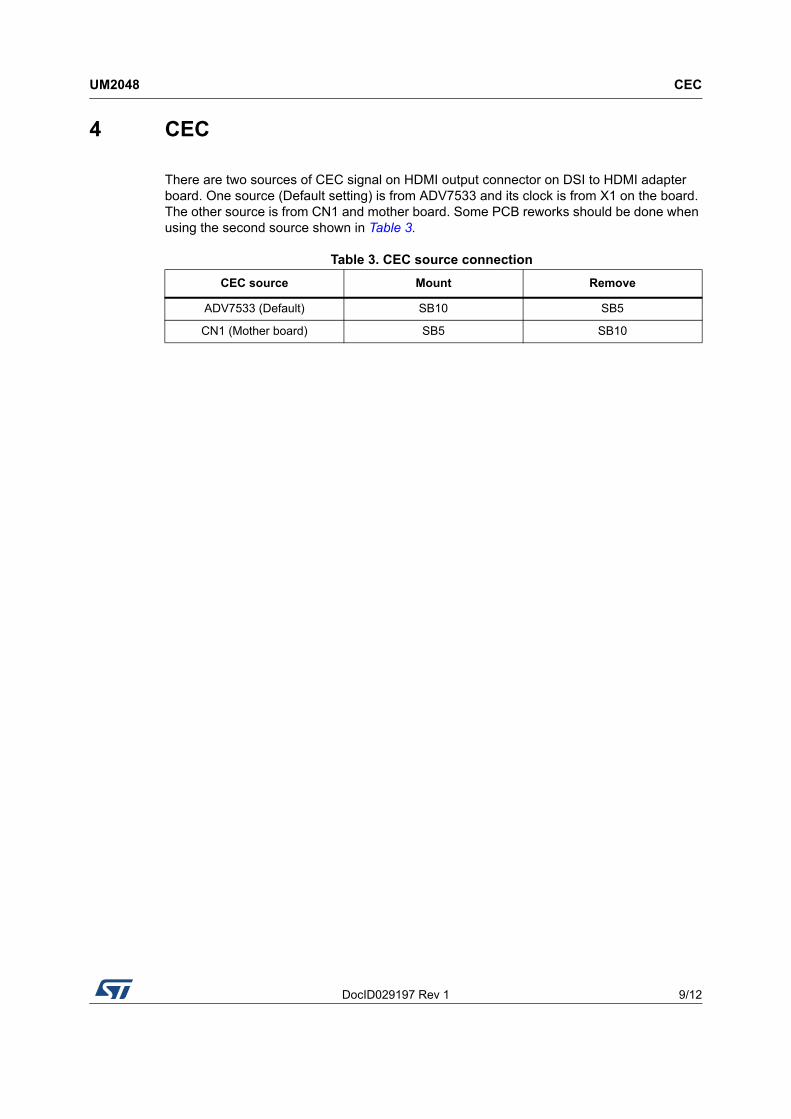
4 CEC
There are two sources of CEC signal on HDMI output connector on DSI to HDMI adapter board. One source (Default setting) is from ADV7533 and its clock is from X1 on the board. The other source is from CN1 and mother board. Some PCB reworks should be done when using the second source shown in Table 3.
Table 3. CEC source connection
CEC source Mount Remove
ADV7533 (Default) SB10 SB5
CN1 (Mother board) SB5 SB10
Sc
he
ma
ticU
M2
048
10/1
2D
ocID029
197 Re
v 1
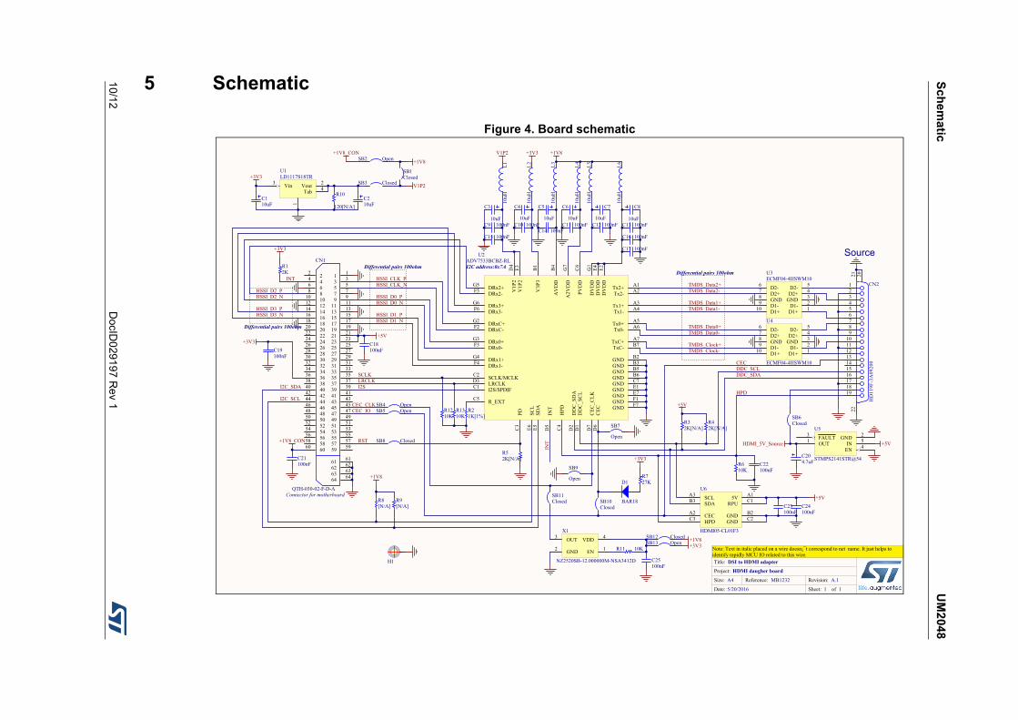
5 Schematic
Figure 4. Board schematic
1 1
DSI to HDMI adapter
MB1232 A.1
5/20/2016
Title:
Size: Reference:
Date: Sheet: of
A4 Revision:
HDMI daugher boardProject:
Source
+5V
C204.7uF
GND 2
IN 5
EN 4OUT1 FAULT3U5
STMPS2141STR@54
HDMI_5V_Source
+5V
TMDS_Data2+TMDS_Data2-
TMDS_Data1+TMDS_Data1-
TMDS_Data0+TMDS_Data0-
TMDS_Clock+TMDS_Clock-
Tx2- A2
GND C7LRCLKD3
V1P
2D4
INT
D5
CEC
D6
GND E7
GND F1
CEC
_CLK
D7
DRx3+G6 Tx1+ A3
GND B5
AVDD
B4
GND B3GND B2
V3P
3B1
PDC3
HPD
C4
R_EXTC5
PVDD
C6
DRx1-F4
DVDD
E4
SDA
E5SC
LE6
GND B6
Tx0+ A5
GND E1
DVDD
E2
V1P
2E3
DVDD
G1
DRxC+G2
DRx0+G3
DRx1+G4
DRx2+G5
DRx2-F5
TxC- B7
DRx3-F6
GND F7
Tx1- A4
Tx2+ A1
DDC_S
DA
D2
DRx0-F3
I2S/SPDIFC1
Tx0- A6
DDC_S
CL
D1
DRxC-F2
SCLK/MCLKC2
TxC+ A7
A2V
DD
G7
U2ADV7533BCBZ-RL
+3V3
I2C_SDA
I2C_SCL
INT
+5V
Connector for motherboard
HSSI_CLK_NHSSI_CLK_P
HSSI_D0_NHSSI_D0_P
HSSI_D1_NHSSI_D1_P
RST
C19100nF
1 122
3 344
5 566
7 788
9 91010
11 111212
13 131414
15 151616
17 171818
19 192020
21 212222
23 232424
25 252626
27 272828
29 293030
31 313232
33 333434
35 353636
37 373838
39 394040
41 414242
43 434444
45 454646
47 474848
49 495050
51 515252
53 535454
55 555656
57 575858
59 596060
61 61
62 62
63 63
64 64
CN1
QTH-030-02-F-D-A
HSSI_D2_NHSSI_D2_P
HSSI_D3_NHSSI_D3_P
SCLKLRCLKI2S
CEC_CLK
INT+1V8_CON
C21100nF
HPD
DDC_SDADDC_SCL
L110
uH
L310
uH
L210
uH
L410
uH
L510
uH
L610
uH
C3
10uFC9 100nF
C15 100nF
+3V3
C10 100nF
C4
10uF
+1V8
C14 100nF
C5
10uFC11 100nF
C6
10uF
C7
10uFC12 100nF
C8
10uFC13 100nF
C16 100nF
C17 100nF
R610K
R8[N/A]
R9[N/A]
+1V8
SB11Closed
R727K
+3V3
D1
BAR18
R21K[1%]
+3V3
CECA2 GND B2
5V A1SCLA3
SDAB3 RPU C1
GND C2HPDC3
U6
HDMI05-CL01F3
CEC
+5VC23100nF
C24100nF
Vin3 Vout 2
1
Tab 4
U1LD1117S18TR
C210uF
+3V3SB3 Closed
SB2 Open +1V8
+1V8_CON
SB8 Closed
SB9
Open
SB7
Open
H1
Note: Text in italic placed on a wire doesn¡¯t correspond to net name. It just helps to identify rapidly MCU IO related to this wire.
SB6Closed
R12K
R52K[N/A]
R32K[N/A]
R42K[N/A]
C22100nF
SB5 Open
SB10Closed
CEC_IO
Differential pairs 100ohm
Differential pairs 100ohm
Differential pairs 100ohm
C18100nF
I2C address:0x7A
C110uF
R10
120[N/A]
SB1Closed
V1P2
V1P2
VDD 4OUT3
EN 1GND2
X1
NZ2520SB-12.000000M-NSA3412D
+3V3
C25100nF
R11 10K
SB4 Open
SB13 OpenSB12 Closed +1V8
R1310K
R1210K
123456789
10111213141516171819
222021
CN2
HD11
9F-3A09
200
GND 3
D1- 2
D1+ 1D1+10 D1-9
D2+ 4D2- 5D2-6
D2+7
GND8
U3ECMF04-4HSWM10
GND 3
D1- 2
D1+ 1D1+10 D1-9
D2+ 4D2- 5D2-6
D2+7
GND8
U4
ECMF04-4HSWM10
DocID029197 Rev 1 11/12
UM2048 Revision history
11
6 Revision history
Table 4. Document revision history
Date Revision Changes
09-Jun-2016 1 Initial release.

UM2048
12/12 DocID029197 Rev 1
IMPORTANT NOTICE – PLEASE READ CAREFULLY
STMicroelectronics NV and its subsidiaries (“ST”) reserve the right to make changes, corrections, enhancements, modifications, and improvements to ST products and/or to this document at any time without notice. Purchasers should obtain the latest relevant information on ST products before placing orders. ST products are sold pursuant to ST’s terms and conditions of sale in place at the time of order acknowledgement.
Purchasers are solely responsible for the choice, selection, and use of ST products and ST assumes no liability for application assistance or the design of Purchasers’ products.
No license, express or implied, to any intellectual property right is granted by ST herein.
Resale of ST products with provisions different from the information set forth herein shall void any warranty granted by ST for such product.
ST and the ST logo are trademarks of ST. All other product or service names are the property of their respective owners.
Information in this document supersedes and replaces information previously supplied in any prior versions of this document.
© 2016 STMicroelectronics – All rights reserved