ds18s20 high-precision 1-wire digital thermometerpark30.wakwak.com/~weather/archive/ds18s20.pdf ·...
TRANSCRIPT

1 of 21 022103
FEATURES� Unique 1-Wire® interface requires only one
port pin for communication� Each device has a unique 64-bit serial code
stored in an onboard ROM� Multidrop capability simplifies distributed
temperature sensing applications� Requires no external components� Can be powered from data line. Power supply
range is 3.0V to 5.5V� Measures temperatures from –55°C to
+125°C (–67°F to +257°F)� �0.5�C accuracy from –10°C to +85°C� 9-bit thermometer resolution� Converts temperature in 750ms (max.)� User-definable nonvolatile (NV) alarm
settings� Alarm search command identifies and
addresses devices whose temperature isoutside of programmed limits (temperaturealarm condition)
� Applications include thermostatic controls,industrial systems, consumer products,thermometers, or any thermally sensitivesystem
PIN ASSIGNMENT
PIN DESCRIPTION GND - GroundDQ - Data In/OutVDD - Power Supply VoltageNC - No Connect
DESCRIPTIONThe DS18S20 Digital Thermometer provides 9-bit centigrade temperature measurements and has analarm function with nonvolatile user-programmable upper and lower trigger points. The DS18S20communicates over a 1-Wire bus that by definition requires only one data line (and ground) forcommunication with a central microprocessor. It has an operating temperature range of –55°C to +125°Cand is accurate to �0.5�C over the range of –10°C to +85°C. In addition, the DS18S20 can derive powerdirectly from the data line (“parasite power”), eliminating the need for an external power supply.
Each DS18S20 has a unique 64-bit serial code, which allows multiple DS18S20s to function on the same1-Wire bus; thus, it is simple to use one microprocessor to control many DS18S20s distributed over alarge area. Applications that can benefit from this feature include HVAC environmental controls,temperature monitoring systems inside buildings, equipment or machinery, and process monitoring andcontrol systems.
DS18S20High-Precision
1-Wire Digital Thermometerwww.maxim-ic.com
8-Pin 150mil SO(DS18S20Z)
TO-92(DS18S20)
1
(BOTTOM VIEW)
2 3
DALLASDS1820
1
GN
DD
QV D
D
2 3NC
NC
NC
NC
GNDDQ
VDD
NC
6
8
7
5
3
1
2
4
DS1820
1-Wire is a registered trademark of Dallas Semiconductor.

DS18S20
2 of 21
DETAILED PIN DESCRIPTIONS Table 18-PIN SOIC* TO-92 SYMBOL DESCRIPTION
5 1 GND Ground.4 2 DQ Data Input/Output Pin. Open-drain 1-Wire interface pin. Also
provides power to the device when used in parasite power mode(see “Parasite Power” section.)
3 3 VDD Optional VDD Pin. VDD must be grounded for operation inparasite power mode.
*All pins not specified in this table are “No Connect” pins.
OVERVIEWFigure 1 shows a block diagram of the DS18S20, and pin descriptions are given in Table 1. The 64-bitROM stores the device’s unique serial code. The scratchpad memory contains the 2-byte temperatureregister that stores the digital output from the temperature sensor. In addition, the scratchpad providesaccess to the 1-byte upper and lower alarm trigger registers (TH and TL). The TH and TL registers arenonvolatile (EEPROM), so they will retain data when the device is powered down.
The DS18S20 uses Dallas’ exclusive 1-Wire bus protocol that implements bus communication using onecontrol signal. The control line requires a weak pullup resistor since all devices are linked to the bus via a3-state or open-drain port (the DQ pin in the case of the DS18S20). In this bus system, the microprocessor(the master device) identifies and addresses devices on the bus using each device’s unique 64-bit code.Because each device has a unique code, the number of devices that can be addressed on one bus isvirtually unlimited. The 1-Wire bus protocol, including detailed explanations of the commands and “timeslots,” is covered in the 1-WIRE BUS SYSTEM section of this datasheet.
Another feature of the DS18S20 is the ability to operate without an external power supply. Power isinstead supplied through the 1-Wire pullup resistor via the DQ pin when the bus is high. The high bussignal also charges an internal capacitor (CPP), which then supplies power to the device when the bus islow. This method of deriving power from the 1-Wire bus is referred to as “parasite power.” As analternative, the DS18S20 may also be powered by an external supply on VDD.
DS18S20 BLOCK DIAGRAM Figure 1VPU
4.7K
POWERSUPPLYSENSE
64-BIT ROMAND
1-wire PORT
DQ
VDD
INTERNAL VDD
CPP
PARASITE POWERCIRCUIT MEMORY CONTROL
LOGIC
SCRATCHPAD
8-BIT CRC GENERATOR
TEMPERATURE SENSOR
ALARM HIGH TRIGGER (TH)REGISTER (EEPROM)
ALARM LOW TRIGGER (TL)REGISTER (EEPROM)
GND
DS18S20

DS18S20
3 of 21
OPERATION — MEASURING TEMPERATUREThe core functionality of the DS18S20 is its direct-to-digital temperature sensor. The temperature sensoroutput has 9-bit resolution, which corresponds to 0.5�C steps. The DS18S20 powers-up in a low-poweridle state; to initiate a temperature measurement and A-to-D conversion, the master must issue a ConvertT [44h] command. Following the conversion, the resulting thermal data is stored in the 2-bytetemperature register in the scratchpad memory and the DS18S20 returns to its idle state. If the DS18S20is powered by an external supply, the master can issue “read-time slots” (see the 1-WIRE BUS SYSTEMsection) after the Convert T command and the DS18S20 will respond by transmitting 0 while thetemperature conversion is in progress and 1 when the conversion is done. If the DS18S20 is powered withparasite power, this notification technique cannot be used since the bus must be pulled high by a strongpullup during the entire temperature conversion. The bus requirements for parasite power are explained indetail in the POWERING THE DS18S20 section of this datasheet.
The DS18S20 output data is calibrated in degrees centigrade; for Fahrenheit applications, a lookup tableor conversion routine must be used. The temperature data is stored as a 16-bit sign-extended two’scomplement number in the temperature register (see Figure 2). The sign bits (S) indicate if thetemperature is positive or negative: for positive numbers S = 0 and for negative numbers S = 1. Table 2gives examples of digital output data and the corresponding temperature reading.
Resolutions greater than 9 bits can be calculated using the data from the temperature, COUNT REMAINand COUNT PER °C registers in the scratchpad. Note that the COUNT PER °C register is hard-wired to16 (10h). After reading the scratchpad, the TEMP_READ value is obtained by truncating the 0.5�C bit(bit 0) from the temperature data (see Figure 2). The extended resolution temperature can then becalculated using the following equation:
CPERCOUNTREMAINCOUNTCPERCOUNTREADTEMPETEMPERATUR
_____25.0_ �
���
TEMPERATURE REGISTER FORMAT Figure 2bit 7 bit 6 bit 5 bit 4 bit 3 bit 2 bit 1 bit 0
LS Byte 26 25 24 23 22 21 20 2-1
bit 15 bit 14 bit 13 bit 12 bit 11 bit 10 bit 9 bit 8
MS Byte S S S S S S S S
TEMPERATURE/DATA RELATIONSHIP Table 2TEMPERATURE DIGITAL OUTPUT
(Binary)DIGITAL OUTPUT
(Hex)+85.0°C* 0000 0000 1010 1010 00AAh+25.0°C 0000 0000 0011 0010 0032h+0.5°C 0000 0000 0000 0001 0001h
0°C 0000 0000 0000 0000 0000h-0.5°C 1111 1111 1111 1111 FFFFh-25.0°C 1111 1111 1100 1110 FFCEh-55.0°C 1111 1111 1001 0010 FF92h
*The power-on reset value of the temperature register is +85°C

DS18S20
4 of 21
OPERATION — ALARM SIGNALINGAfter the DS18S20 performs a temperature conversion, the temperature value is compared to the user-defined two’s complement alarm trigger values stored in the 1-byte TH and TL registers (see Figure 3).The sign bit (S) indicates if the value is positive or negative: for positive numbers S = 0 and for negativenumbers S = 1. The TH and TL registers are nonvolatile (EEPROM) so they will retain data when thedevice is powered down. TH and TL can be accessed through bytes 2 and 3 of the scratchpad as explainedin the MEMORY section of this datasheet.
TH AND TL REGISTER FORMAT Figure 3bit 7 bit 6 bit 5 bit 4 bit 3 bit 2 bit 1 bit 0
S 26 25 25 25 22 21 20
Only bits 8 through 1 of the temperature register are used in the TH and TL comparison since TH and TLare 8-bit registers. If the measured temperature is lower than or equal to TL or higher than TH, an alarmcondition exists and an alarm flag is set inside the DS18S20. This flag is updated after every temperaturemeasurement; therefore, if the alarm condition goes away, the flag will be turned off after the nexttemperature conversion.
The master device can check the alarm flag status of all DS18S20s on the bus by issuing an Alarm Search[ECh] command. Any DS18S20s with a set alarm flag will respond to the command, so the master candetermine exactly which DS18S20s have experienced an alarm condition. If an alarm condition exists andthe TH or TL settings have changed, another temperature conversion should be done to validate the alarmcondition.
POWERING THE DS18S20The DS18S20 can be powered by an external supply on the VDD pin, or it can operate in “parasite power”mode, which allows the DS18S20 to function without a local external supply. Parasite power is veryuseful for applications that require remote temperature sensing or that are very space constrained. Figure1 shows the DS18S20’s parasite-power control circuitry, which “steals” power from the 1-Wire bus viathe DQ pin when the bus is high. The stolen charge powers the DS18S20 while the bus is high, and someof the charge is stored on the parasite power capacitor (CPP) to provide power when the bus is low. Whenthe DS18S20 is used in parasite power mode, the VDD pin must be connected to ground.
In parasite power mode, the 1-Wire bus and CPP can provide sufficient current to the DS18S20 for mostoperations as long as the specified timing and voltage requirements are met (refer to the DCELECTRICAL CHARACTERISTICS and the AC ELECTRICAL CHARACTERISTICS sections of this datasheet). However, when the DS18S20 is performing temperature conversions or copying data from thescratchpad memory to EEPROM, the operating current can be as high as 1.5mA. This current can causean unacceptable voltage drop across the weak 1-Wire pullup resistor and is more current than can besupplied by CPP. To assure that the DS18S20 has sufficient supply current, it is necessary to provide astrong pullup on the 1-Wire bus whenever temperature conversions are taking place or data is beingcopied from the scratchpad to EEPROM. This can be accomplished by using a MOSFET to pull the busdirectly to the rail as shown in Figure 4. The 1-Wire bus must be switched to the strong pullup within10�s (max) after a Convert T [44h] or Copy Scratchpad [48h] command is issued, and the bus must beheld high by the pullup for the duration of the conversion (tconv) or data transfer (twr = 10ms). No otheractivity can take place on the 1-Wire bus while the pullup is enabled.
The DS18S20 can also be powered by the conventional method of connecting an external power supply tothe VDD pin, as shown in Figure 5. The advantage of this method is that the MOSFET pullup is notrequired, and the 1-Wire bus is free to carry other traffic during the temperature conversion time.

DS18S20
5 of 21
The use of parasite power is not recommended for temperatures above 100�C since the DS18S20 may notbe able to sustain communications due to the higher leakage currents that can exist at these temperatures.For applications in which such temperatures are likely, it is strongly recommended that the DS18S20 bepowered by an external power supply.
In some situations the bus master may not know whether the DS18S20s on the bus are parasite poweredor powered by external supplies. The master needs this information to determine if the strong bus pullupshould be used during temperature conversions. To get this information, the master can issue a Skip ROM[CCh] command followed by a Read Power Supply [B4h] command followed by a “read-time slot”.During the read-time slot, parasite powered DS18S20s will pull the bus low, and externally poweredDS18S20s will let the bus remain high. If the bus is pulled low, the master knows that it must supply thestrong pullup on the 1-Wire bus during temperature conversions.
SUPPLYING THE PARASITE-POWERED DS18S20 DURING TEMPERATURECONVERSIONS Figure 4
POWERING THE DS18S20 WITH AN EXTERNAL SUPPLY Figure 5
64-BIT LASERED ROM CODEEach DS18S20 contains a unique 64-bit code (see Figure 6) stored in ROM. The least significant 8 bits ofthe ROM code contain the DS18S20’s 1-Wire family code: 10h. The next 48 bits contain a unique serialnumber. The most significant 8 bits contain a cyclic redundancy check (CRC) byte that is calculated fromthe first 56 bits of the ROM code. A detailed explanation of the CRC bits is provided in the CRCGENERATION section. The 64-bit ROM code and associated ROM function control logic allow theDS18S20 to operate as a 1-Wire device using the protocol detailed in the 1-WIRE BUS SYSTEM sectionof this datasheet.
64-BIT LASERED ROM CODE Figure 68-BIT CRC 48-BIT SERIAL NUMBER 8-BIT FAMILY CODE (10h)
MSB MSBLSB LSB LSBMSB
VDD (External Supply)DS18S20GND VDDDQ
VPU
4.7kTo Other1-Wire Devices1-Wire Bus
Micro-processor
VPU
VPU
4.7k1-Wire Bus
Micro-processor
DS18S20GND VDDDQ
To Other1-Wire Devices
DS18S20
6 of 21
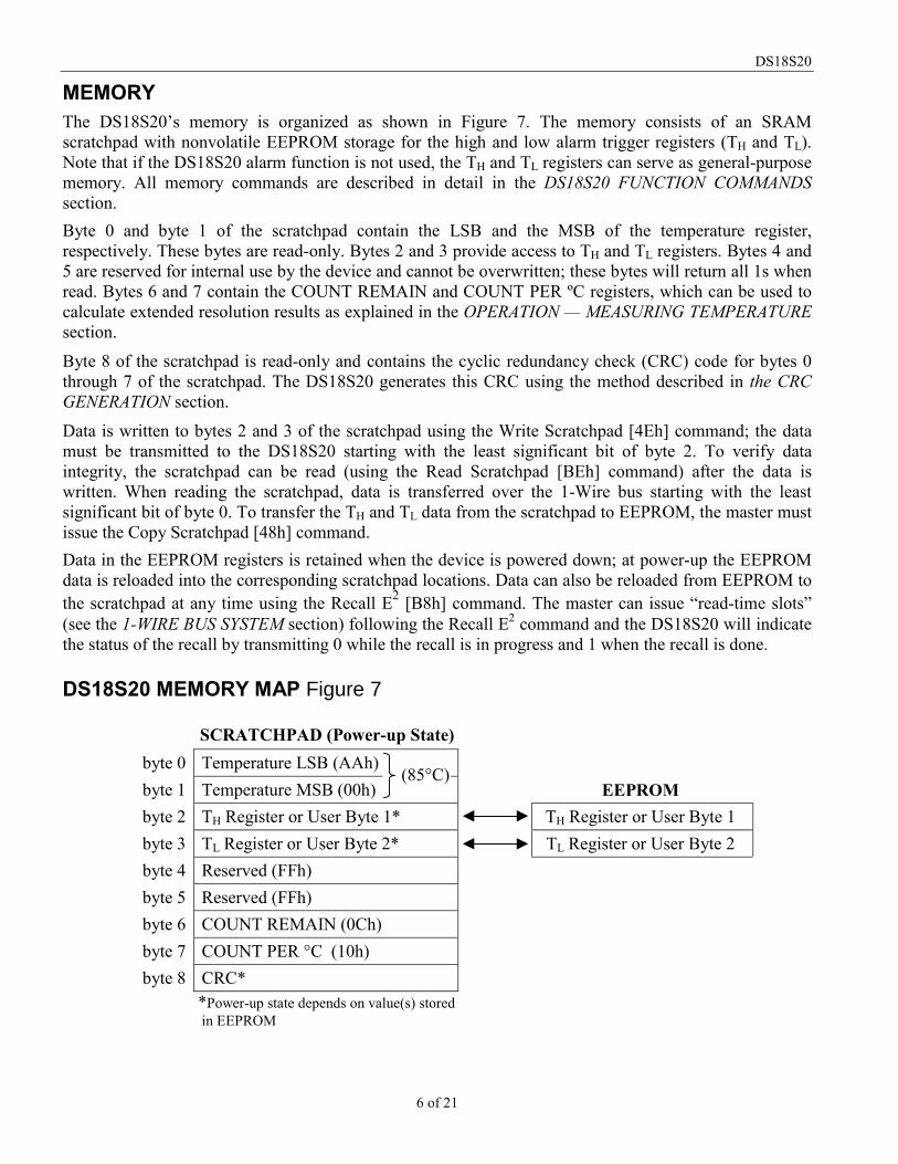
MEMORYThe DS18S20’s memory is organized as shown in Figure 7. The memory consists of an SRAMscratchpad with nonvolatile EEPROM storage for the high and low alarm trigger registers (TH and TL).Note that if the DS18S20 alarm function is not used, the TH and TL registers can serve as general-purposememory. All memory commands are described in detail in the DS18S20 FUNCTION COMMANDSsection.Byte 0 and byte 1 of the scratchpad contain the LSB and the MSB of the temperature register,respectively. These bytes are read-only. Bytes 2 and 3 provide access to TH and TL registers. Bytes 4 and5 are reserved for internal use by the device and cannot be overwritten; these bytes will return all 1s whenread. Bytes 6 and 7 contain the COUNT REMAIN and COUNT PER ºC registers, which can be used tocalculate extended resolution results as explained in the OPERATION — MEASURING TEMPERATUREsection.
Byte 8 of the scratchpad is read-only and contains the cyclic redundancy check (CRC) code for bytes 0through 7 of the scratchpad. The DS18S20 generates this CRC using the method described in the CRCGENERATION section.
Data is written to bytes 2 and 3 of the scratchpad using the Write Scratchpad [4Eh] command; the datamust be transmitted to the DS18S20 starting with the least significant bit of byte 2. To verify dataintegrity, the scratchpad can be read (using the Read Scratchpad [BEh] command) after the data iswritten. When reading the scratchpad, data is transferred over the 1-Wire bus starting with the leastsignificant bit of byte 0. To transfer the TH and TL data from the scratchpad to EEPROM, the master mustissue the Copy Scratchpad [48h] command.Data in the EEPROM registers is retained when the device is powered down; at power-up the EEPROMdata is reloaded into the corresponding scratchpad locations. Data can also be reloaded from EEPROM tothe scratchpad at any time using the Recall E2 [B8h] command. The master can issue “read-time slots”(see the 1-WIRE BUS SYSTEM section) following the Recall E2 command and the DS18S20 will indicatethe status of the recall by transmitting 0 while the recall is in progress and 1 when the recall is done.
DS18S20 MEMORY MAP Figure 7
SCRATCHPAD (Power-up State)byte 0 Temperature LSB (AAh)byte 1 Temperature MSB (00h) EEPROMbyte 2 TH Register or User Byte 1* TH Register or User Byte 1byte 3 TL Register or User Byte 2* TL Register or User Byte 2byte 4 Reserved (FFh)byte 5 Reserved (FFh)byte 6 COUNT REMAIN (0Ch)byte 7 COUNT PER °C (10h)byte 8 CRC*
*Power-up state depends on value(s) stored in EEPROM
(85°C)

DS18S20
7 of 21
CRC GENERATIONCRC bytes are provided as part of the DS18S20’s 64-bit ROM code and in the 9th byte of the scratchpadmemory. The ROM code CRC is calculated from the first 56 bits of the ROM code and is contained in themost significant byte of the ROM. The scratchpad CRC is calculated from the data stored in thescratchpad, and therefore it changes when the data in the scratchpad changes. The CRCs provide the busmaster with a method of data validation when data is read from the DS18S20. To verify that data hasbeen read correctly, the bus master must re-calculate the CRC from the received data and then comparethis value to either the ROM code CRC (for ROM reads) or to the scratchpad CRC (for scratchpad reads).If the calculated CRC matches the read CRC, the data has been received error free. The comparison ofCRC values and the decision to continue with an operation are determined entirely by the bus master.There is no circuitry inside the DS18S20 that prevents a command sequence from proceeding if theDS18S20 CRC (ROM or scratchpad) does not match the value generated by the bus master.
The equivalent polynomial function of the CRC (ROM or scratchpad) is:
CRC = X8 + X5 + X4 + 1
The bus master can re-calculate the CRC and compare it to the CRC values from the DS18S20 using thepolynomial generator shown in Figure 8. This circuit consists of a shift register and XOR gates, and theshift register bits are initialized to 0. Starting with the least significant bit of the ROM code or the leastsignificant bit of byte 0 in the scratchpad, one bit at a time should shifted into the shift register. Aftershifting in the 56th bit from the ROM or the most significant bit of byte 7 from the scratchpad, thepolynomial generator will contain the re-calculated CRC. Next, the 8-bit ROM code or scratchpad CRCfrom the DS18S20 must be shifted into the circuit. At this point, if the re-calculated CRC was correct, theshift register will contain all 0s. Additional information about the Dallas 1-Wire cyclic redundancy checkis available in Application Note 27: Understanding and Using Cyclic Redundancy Checks with DallasSemiconductor Touch Memory Products.
CRC GENERATOR Figure 8
(MSB) (LSB)
XOR XOR XOR
INPUT

DS18S20
8 of 21
1-WIRE BUS SYSTEMThe 1-Wire bus system uses a single bus master to control one or more slave devices. The DS18S20 isalways a slave. When there is only one slave on the bus, the system is referred to as a “single-drop”system; the system is “multidrop” if there are multiple slaves on the bus.
All data and commands are transmitted least significant bit first over the 1-Wire bus.
The following discussion of the 1-Wire bus system is broken down into three topics: hardwareconfiguration, transaction sequence, and 1-Wire signaling (signal types and timing).
HARDWARE CONFIGURATIONThe 1-Wire bus has by definition only a single data line. Each device (master or slave) interfaces to thedata line via an open drain or 3-state port. This allows each device to “release” the data line when thedevice is not transmitting data so the bus is available for use by another device. The 1-Wire port of theDS18S20 (the DQ pin) is open drain with an internal circuit equivalent to that shown in Figure 9.
The 1-Wire bus requires an external pullup resistor of approximately 5k�; thus, the idle state for the 1-Wire bus is high. If for any reason a transaction needs to be suspended, the bus MUST be left in the idlestate if the transaction is to resume. Infinite recovery time can occur between bits so long as the 1-Wirebus is in the inactive (high) state during the recovery period. If the bus is held low for more than 480�s,all components on the bus will be reset.
HARDWARE CONFIGURATION Figure 9
TRANSACTION SEQUENCEThe transaction sequence for accessing the DS18S20 is as follows:
Step 1. Initialization
Step 2. ROM Command (followed by any required data exchange)
Step 3. DS18S20 Function Command (followed by any required data exchange)
It is very important to follow this sequence every time the DS18S20 is accessed, as the DS18S20 will notrespond if any steps in the sequence are missing or out of order. Exceptions to this rule are the SearchROM [F0h] and Alarm Search [ECh] commands. After issuing either of these ROM commands, themaster must return to Step 1 in the sequence.
VPU
4.7k
5µATyp.
RX
TX
DS18S20 1-WIRE PORT
100�MOSFET
TX
RX
RX = RECEIVETX = TRANSMIT
1-wire Bus
DQPin
DS18S20
9 of 21
INITIALIZATIONAll transactions on the 1-Wire bus begin with an initialization sequence. The initialization sequenceconsists of a reset pulse transmitted by the bus master followed by presence pulse(s) transmitted by theslave(s). The presence pulse lets the bus master know that slave devices (such as the DS18S20) are on thebus and are ready to operate. Timing for the reset and presence pulses is detailed in the1-WIRE SIGNALING section.
ROM COMMANDSAfter the bus master has detected a presence pulse, it can issue a ROM command. These commandsoperate on the unique 64-bit ROM codes of each slave device and allow the master to single out a specificdevice if many are present on the 1-Wire bus. These commands also allow the master to determine howmany and what types of devices are present on the bus or if any device has experienced an alarmcondition. There are five ROM commands, and each command is 8 bits long. The master device mustissue an appropriate ROM command before issuing a DS18S20 function command. A flowchart foroperation of the ROM commands is shown in Figure 14.
SEARCH ROM [F0h]When a system is initially powered up, the master must identify the ROM codes of all slave devices onthe bus, which allows the master to determine the number of slaves and their device types. The masterlearns the ROM codes through a process of elimination that requires the master to perform a Search ROMcycle (i.e., Search ROM command followed by data exchange) as many times as necessary to identify allof the slave devices. If there is only one slave on the bus, the simpler Read ROM command (see below)can be used in place of the Search ROM process. For a detailed explanation of the Search ROMprocedure, refer to the iButton® Book of Standards at www.ibutton.com/ibuttons/standard.pdf. Afterevery Search ROM cycle, the bus master must return to Step 1 (Initialization) in the transaction sequence.
READ ROM [33h]This command can only be used when there is one slave on the bus. It allows the bus master to read theslave’s 64-bit ROM code without using the Search ROM procedure. If this command is used when thereis more than one slave present on the bus, a data collision will occur when all the slaves attempt torespond at the same time.
MATCH ROM [55h]The match ROM command followed by a 64-bit ROM code sequence allows the bus master to address aspecific slave device on a multidrop or single-drop bus. Only the slave that exactly matches the 64-bitROM code sequence will respond to the function command issued by the master; all other slaves on thebus will wait for a reset pulse.
SKIP ROM [CCh]The master can use this command to address all devices on the bus simultaneously without sending outany ROM code information. For example, the master can make all DS18S20s on the bus performsimultaneous temperature conversions by issuing a Skip ROM command followed by a Convert T [44h]command.
Note that the Read Scratchpad [BEh] command can follow the Skip ROM command only if there is asingle slave device on the bus. In this case time is saved by allowing the master to read from the slavewithout sending the device’s 64-bit ROM code. A Skip ROM command followed by a Read Scratchpadcommand will cause a data collision on the bus if there is more than one slave since multiple devices willattempt to transmit data simultaneously.
iButton is a registered trademark of Dallas Semiconductor.

DS18S20
10 of 21
ALARM SEARCH [ECh]The operation of this command is identical to the operation of the Search ROM command except thatonly slaves with a set alarm flag will respond. This command allows the master device to determine ifany DS18S20s experienced an alarm condition during the most recent temperature conversion. Afterevery Alarm Search cycle (i.e., Alarm Search command followed by data exchange), the bus master mustreturn to Step 1 (Initialization) in the transaction sequence. Refer to the OPERATION — ALARMSIGNALING section for an explanation of alarm flag operation.
DS18S20 FUNCTION COMMANDSAfter the bus master has used a ROM command to address the DS18S20 with which it wishes tocommunicate, the master can issue one of the DS18S20 function commands. These commands allow themaster to write to and read from the DS18S20’s scratchpad memory, initiate temperature conversions anddetermine the power supply mode. The DS18S20 function commands, which are described below, aresummarized in Table 4 and illustrated by the flowchart in Figure 15.
CONVERT T [44h]This command initiates a single temperature conversion. Following the conversion, the resulting thermaldata is stored in the 2-byte temperature register in the scratchpad memory and the DS18S20 returns to itslow-power idle state. If the device is being used in parasite power mode, within 10�s (max) after thiscommand is issued the master must enable a strong pullup on the 1-Wire bus for the duration of theconversion (tconv) as described in the POWERING THE DS18S20 section. If the DS18S20 is powered byan external supply, the master can issue read-time slots after the Convert T command and the DS18S20will respond by transmitting 0 while the temperature conversion is in progress and 1 when the conversionis done. In parasite power mode this notification technique cannot be used since the bus is pulled high bythe strong pullup during the conversion.
WRITE SCRATCHPAD [4Eh]This command allows the master to write 2 bytes of data to the DS18S20’s scratchpad. The first byte iswritten into the TH register (byte 2 of the scratchpad), and the second byte is written into the TL register(byte 3 of the scratchpad). Data must be transmitted least significant bit first. Both bytes MUST bewritten before the master issues a reset, or the data may be corrupted.
READ SCRATCHPAD [BEh]This command allows the master to read the contents of the scratchpad. The data transfer starts with theleast significant bit of byte 0 and continues through the scratchpad until the 9th byte (byte 8 – CRC) isread. The master may issue a reset to terminate reading at any time if only part of the scratchpad data isneeded.
COPY SCRATCHPAD [48h]This command copies the contents of the scratchpad TH and TL registers (bytes 2 and 3) to EEPROM. Ifthe device is being used in parasite power mode, within 10�s (max) after this command is issued themaster must enable a strong pullup on the 1-Wire bus for at least 10ms as described in the POWERINGTHE DS18S20 section.
RECALL E2 [B8h]This command recalls the alarm trigger values (TH and TL) from EEPROM and places the data in bytes 2and 3, respectively, in the scratchpad memory. The master device can issue read-time slots following theRecall E2 command and the DS18S20 will indicate the status of the recall by transmitting 0 while therecall is in progress and 1 when the recall is done. The recall operation happens automatically at power-up, so valid data is available in the scratchpad as soon as power is applied to the device.
DS18S20
11 of 21
READ POWER SUPPLY [B4h]The master device issues this command followed by a read-time slot to determine if any DS18S20s on thebus are using parasite power. During the read-time slot, parasite powered DS18S20s will pull the bus low,and externally powered DS18S20s will let the bus remain high. Refer to the POWERING THE DS18S20section for usage information for this command.
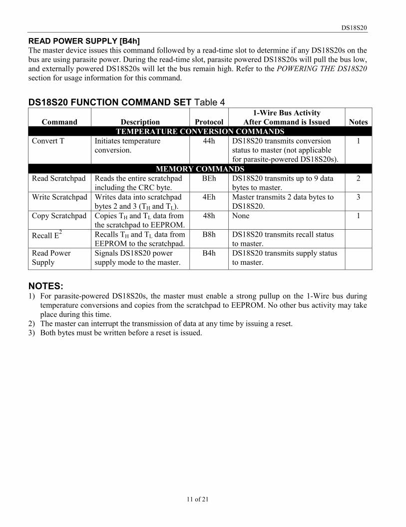
DS18S20 FUNCTION COMMAND SET Table 4
Command Description Protocol1-Wire Bus Activity
After Command is Issued NotesTEMPERATURE CONVERSION COMMANDS
Convert T Initiates temperatureconversion.
44h DS18S20 transmits conversionstatus to master (not applicablefor parasite-powered DS18S20s).
1
MEMORY COMMANDSRead Scratchpad Reads the entire scratchpad
including the CRC byte.BEh DS18S20 transmits up to 9 data
bytes to master.2
Write Scratchpad Writes data into scratchpadbytes 2 and 3 (TH and TL).
4Eh Master transmits 2 data bytes toDS18S20.
3
Copy Scratchpad Copies TH and TL data fromthe scratchpad to EEPROM.
48h None 1
Recall E2 Recalls TH and TL data fromEEPROM to the scratchpad.
B8h DS18S20 transmits recall statusto master.
Read PowerSupply
Signals DS18S20 powersupply mode to the master.
B4h DS18S20 transmits supply statusto master.
NOTES:1) For parasite-powered DS18S20s, the master must enable a strong pullup on the 1-Wire bus during
temperature conversions and copies from the scratchpad to EEPROM. No other bus activity may takeplace during this time.
2) The master can interrupt the transmission of data at any time by issuing a reset.3) Both bytes must be written before a reset is issued.

DS18S20
12 of 21
1-WIRE SIGNALINGThe DS18S20 uses a strict 1-Wire communication protocol to insure data integrity. Several signal typesare defined by this protocol: reset pulse, presence pulse, write 0, write 1, read 0, and read 1. All of thesesignals, with the exception of the presence pulse, are initiated by the bus master.
INITIALIZATION PROCEDURE: RESET AND PRESENCE PULSESAll communication with the DS18S20 begins with an initialization sequence that consists of a reset pulsefrom the master followed by a presence pulse from the DS18S20. This is illustrated in Figure 10. Whenthe DS18S20 sends the presence pulse in response to the reset, it is indicating to the master that it is onthe bus and ready to operate.
During the initialization sequence the bus master transmits (TX) the reset pulse by pulling the 1-Wire buslow for a minimum of 480�s. The bus master then releases the bus and goes into receive mode (RX).When the bus is released, the 5k pullup resistor pulls the 1-Wire bus high. When the DS18S20 detectsthis rising edge, it waits 15�s to 60�s and then transmits a presence pulse by pulling the 1-Wire bus lowfor 60�s to 240�s.
INITIALIZATION TIMING Figure 10
READ/WRITE TIME SLOTSThe bus master writes data to the DS18S20 during write time slots and reads data from the DS18S20during read-time slots. One bit of data is transmitted over the 1-Wire bus per time slot.
WRITE TIME SLOTSThere are two types of write time slots: “Write 1” time slots and “Write 0” time slots. The bus masteruses a Write 1 time slot to write a logic 1 to the DS18S20 and a Write 0 time slot to write a logic 0 to theDS18S20. All write time slots must be a minimum of 60�s in duration with a minimum of a 1�s recoverytime between individual write slots. Both types of write time slots are initiated by the master pulling the1-Wire bus low (see Figure 11).
To generate a Write 1 time slot, after pulling the 1-Wire bus low, the bus master must release the 1-Wirebus within 15�s. When the bus is released, the 5k pullup resistor will pull the bus high. To generate aWrite 0 time slot, after pulling the 1-Wire bus low, the bus master must continue to hold the bus low forthe duration of the time slot (at least 60�s). The DS18S20 samples the 1-Wire bus during a window thatlasts from 15�s to 60�s after the master initiates the write time slot. If the bus is high during the samplingwindow, a 1 is written to the DS18S20. If the line is low, a 0 is written to the DS18S20.
LINE TYPE LEGENDBus master pulling lowDS18S20 pulling lowResistor pullup
VPU
GND
1-WIRE BUS
480�s minimum 480�s minimumDS18S20 TX
presence pulse60-240 �s
MASTER TX RESET PULSE MASTER RX
DS18S20 waits 15-60 �s

DS18S20
13 of 21
READ-TIME SLOTSThe DS18S20 can only transmit data to the master when the master issues read-time slots. Therefore, themaster must generate read-time slots immediately after issuing a Read Scratchpad [BEh] or Read PowerSupply [B4h] command, so that the DS18S20 can provide the requested data. In addition, the master cangenerate read-time slots after issuing Convert T [44h] or Recall E2 [B8h] commands to find out the statusof the operation as explained in the DS18S20 FUNCTION COMMAND section.
All read-time slots must be a minimum of 60�s in duration with a minimum of a 1�s recovery timebetween slots. A read-time slot is initiated by the master device pulling the 1-Wire bus low for aminimum of 1�s and then releasing the bus (see Figure 11). After the master initiates the read-time slot,the DS18S20 will begin transmitting a 1 or 0 on bus. The DS18S20 transmits a 1 by leaving the bus highand transmits a 0 by pulling the bus low. When transmitting a 0, the DS18S20 will release the bus by theend of the time slot, and the bus will be pulled back to its high idle state by the pullup resister. Outputdata from the DS18S20 is valid for 15�s after the falling edge that initiated the read-time slot. Therefore,the master must release the bus and then sample the bus state within 15�s from the start of the slot.
Figure 12 illustrates that the sum of TINIT, TRC, and TSAMPLE must be less than 15�s for a read-time slot.Figure 13 shows that system timing margin is maximized by keeping TINIT and TRC as short as possibleand by locating the master sample time during read-time slots towards the end of the 15�s period.
READ/WRITE TIME SLOT TIMING DIAGRAM Figure 11
45�s15�s
VPU
GND
1-WIRE BUS
60�s < TX “0” < 120�s1�s < TREC < �
DS18S20 SamplesMIN TYP MAX
15�s 30�s
> 1�s
MASTER WRITE “0” SLOT MASTER WRITE “1” SLOT
VPU
GND
1-WIRE BUS
15�s
MASTER READ “0” SLOT MASTER READ “1” SLOT
Master samples Master samples
STARTOF SLOT
STARTOF SLOT
> 1 �s
1�s < TREC < �
15�s 15�s 30�s15�s
DS18S20 SamplesMIN TYP MAX
> 1�s
LINE TYPE LEGENDBus master pulling low DS18S20 pulling low
Resistor pullup

DS18S20
14 of 21
DETAILED MASTER READ 1 TIMING Figure 12
RECOMMENDED MASTER READ 1 TIMING Figure 13
VPU
GND
1-WIRE BUS
15�s
VIH of Master
TRCTINT > 1�s Master samples
LINE TYPE LEGENDBus master pulling lowResistor pullup
VPU
GND
1-WIRE BUS
15�s
VIH of Master
TRC =small
TINT =small
Master samples

DS18S20
15 of 21
ROM COMMANDS FLOW CHART Figure 14
CChSKIP ROMCOMMAND
MASTER TXRESET PULSE
DS18S20 TXPRESENCE
PULSE
MASTER TX ROMCOMMAND
33hREAD ROMCOMMAND
55hMATCH ROMCOMMAND
F0hSEARCH ROM
COMMAND
EChALARM SEARCH
COMMAND
MASTER TXBIT 0
DS18S20 TX BIT 0
DS18S20 TX BIT 0
MASTER TX BIT 0
BIT 0MATCH?
MASTER TXBIT 1
BIT 1MATCH?
BIT 63MATCH?
MASTER TXBIT 63
N
Y Y Y Y Y
N N N N
N
N
N
Y
Y
Y
DS18S20 TX BIT 1
DS18S20 TX BIT 1
MASTER TX BIT 1
DS18S20 TX BIT 63
DS18S20 TX BIT 63
MASTER TX BIT 63
BIT 0MATCH?
BIT 1MATCH?
BIT 63MATCH?
N
N
N
Y
Y
Y
DS18S20 TXFAMILY CODE
1 BYTE
DS18S20 TXSERIAL NUMBER
6 BYTES
DS18S20 TXCRC BYTE
DS18S20 TX BIT 0
DS18S20 TX BIT 0
MASTER TX BIT 0
N
Y
DEVICE(S)WITH ALARMFLAG SET?
InitializationSequence
MASTER TXFUNCTIONCOMMAND
(FIGURE 15)

DS18S20
16 of 21
DS18S20 FUNCTION COMMANDS FLOW CHART Figure 15
MASTER TXFUNCTIONCOMMAND
Y
N44h
CONVERTTEMPERATURE
?
PARASITEPOWER
?
N Y
DS18S20 BEGINSCONVERSION
DEVICECONVERTING
TEMPERATURE?
N
Y
MASTERRX “0s”
MASTERRX “1s”
MASTER ENABLESSTRONG PULLUP ON DQ
DS18S20 CONVERTSTEMPERATURE
MASTER DISABLESSTRONG PULLUP
Y
N48h
COPYSCRATCHPAD
?
PARASITEPOWER
?
N Y
MASTER ENABLESSTRONG PULL-UP ON DQ
DATA COPIED FROMSCRATCHPAD TO EEPROM
MASTER DISABLESSTRONG PULLUP
MASTERRX “0s”
COPY INPROGRESS
?
Y
MASTERRX “1s”
N
RETURN TO INITIALIZATIONSEQUENCE (FIGURE 14) FOR
NEXT TRANSACTION
B4hREAD
POWER SUPPLY?
Y
N
PARASITEPOWERED
?
N
MASTERRX “1s”
MASTERRX “0s”
Y
MASTER TX TH BYTETO SCRATCHPAD
Y
N4Eh
WRITESCRATCHPAD
?
MASTER TX TL BYTETO SCRATCHPAD
Y
N
Y
BEhREAD
SCRATCHPAD?
HAVE 8 BYTESBEEN READ
?
N
MASTERTX RESET
?
MASTER RX DATA BYTEFROM SCRATCHPAD
N
Y
MASTER RX SCRATCHPADCRC BYTE
MASTERRX “1s”
Y
N B8hRECALL E2
?
MASTER BEGINS DATARECALL FROM E2 PROM
DEVICEBUSY RECALLING
DATA?
N
Y
MASTERRX “0s”

DS18S20
17 of 21
DS18S20 OPERATION EXAMPLE 1In this example there are multiple DS18S20s on the bus and they are using parasite power. The busmaster initiates a temperature conversion in a specific DS18S20 and then reads its scratchpad andrecalculates the CRC to verify the data.
MASTER MODE DATA (LSB FIRST) COMMENTSTX Reset Master issues reset pulse.RX Presence DS18S20s respond with presence pulse.TX 55h Master issues Match ROM command.TX 64-bit ROM code Master sends DS18S20 ROM code.TX 44h Master issues Convert T command.TX DQ line held high by
strong pullupMaster applies strong pullup to DQ for the duration of theconversion (tconv).
TX Reset Master issues reset pulse.RX Presence DS18S20s respond with presence pulse.TX 55h Master issues Match ROM command.TX 64-bit ROM code Master sends DS18S20 ROM code.TX BEh Master issues Read Scratchpad command.RX 9 data bytes Master reads entire scratchpad including CRC. The master
then recalculates the CRC of the first eight data bytes from thescratchpad and compares the calculated CRC with the readCRC (byte 9). If they match, the master continues; if not, theread operation is repeated.
DS18S20 OPERATION EXAMPLE 2In this example there is only one DS18S20 on the bus and it is using parasite power. The master writes tothe TH and TL registers in the DS18S20 scratchpad and then reads the scratchpad and recalculates theCRC to verify the data. The master then copies the scratchpad contents to EEPROM.
MASTER MODE DATA (LSB FIRST) COMMENTSTX Reset Master issues reset pulse.RX Presence DS18S20 responds with presence pulse.TX CCh Master issues Skip ROM command.TX 4Eh Master issues Write Scratchpad command.TX 2 data bytes Master sends two data bytes to scratchpad (TH and TL)TX Reset Master issues reset pulse.RX Presence DS18S20 responds with presence pulse.TX CCh Master issues Skip ROM command.TX BEh Master issues Read Scratchpad command.RX 9 data bytes Master reads entire scratchpad including CRC. The master then
recalculates the CRC of the first eight data bytes from thescratchpad and compares the calculated CRC with the read CRC(byte 9). If they match, the master continues; if not, the readoperation is repeated.
TX Reset Master issues reset pulse.RX Presence DS18S20 responds with presence pulse.TX CCh Master issues Skip ROM command.TX 48h Master issues Copy Scratchpad command.TX DQ line held high by
strong pullupMaster applies strong pullup to DQ for at least 10ms while copyoperation is in progress.

DS18S20
18 of 21
DS18S20 OPERATION EXAMPLE 3In this example there is only one DS18S20 on the bus and it is using parasite power. The bus masterinitiates a temperature conversion then reads the DS18S20 scratchpad and calculates a higher resolutionresult using the data from the temperature, COUNT REMAIN and COUNT PER °C registers.
MASTER MODE DATA (LSB FIRST) COMMENTSTX Reset Master issues reset pulse.TR Presence DS18S20 responds with presence pulse.TX CCh Master issues Skip ROM command.TX 44h Master issues Convert T command.TX DQ line held high by
strong pullupMaster applies strong pullup to DQ for the duration of theconversion (tconv).
TX Reset Master issues reset pulse.RX Presence DS18S20 responds with presence pulse.TX CCh Master issues Skip ROM command.TX BEh Master issues Read Scratchpad command.RX 9 data bytes Master reads entire scratchpad including CRC. The master
then recalculates the CRC of the first eight data bytes from thescratchpad and compares the calculated CRC with the readCRC (byte 9). If they match, the master continues; if not, theread operation is repeated. The master also calculates theTEMP_READ value and stores the contents of the COUNTREMAIN and COUNT PER °C registers.
TX Reset Master issues reset pulse.RX Presence DS18S20 responds with presence pulse.
- - CPU calculates extended resolution temperature using theequation in the OPERATION — MEASURINGTEMPERATURE section of this datasheet.

DS18S20
19 of 21
ABSOLUTE MAXIMUM RATINGS*Voltage on Any Pin Relative to Ground -0.5V to +6.0VOperating Temperature Range -55�C to +125�CStorage Temperature Range -55�C to +125�CSolder Temperature See IPC/JEDEC J-STD-020AReflow Oven Temperature +220°C
*These are stress ratings only and functional operation of the device at these or any other conditionsabove those indicated in the operation sections of this specification is not implied. Exposure to absolutemaximum rating conditions for extended periods of time may affect reliability.
DC ELECTRICAL CHARACTERISTICS (-55°C to +125°C; VDD = 3.0V to 5.5V)PARAMETER SYMBOL CONDITION MIN TYP MAX UNITS NOTESSupply Voltage VDD Local Power +3.0 +5.5 V 1
Parasite Power +3.0 +5.5Pullup SupplyVoltage
VPULocal Power +3.0 VDD
V 1, 2
-10°C to+85°C
±0.5 °C 3Thermometer Error tERR
-55°C to+125°C
±2
Input Logic Low VIL -0.3 +0.8 V 1, 4, 5Local Power +2.2Input Logic High VIH
Parasite Power +3.0
The lower of5.5or
VDD + 0.3
V 1, 6
Sink Current IL VI/O=0.4V 4.0 mA 1Standby Current IDDS 750 1000 nA 7, 8Active Current IDD VDD=5V 1 1.5 mA 9DQ Input Current IDQ 5 µA 10Drift ±0.2 °C 11
NOTES:1) All voltages are referenced to ground.2) The Pullup Supply Voltage specification assumes that the pullup device is ideal, and therefore the
high level of the pullup is equal to VPU. In order to meet the VIH spec of the DS18S20, the actualsupply rail for the strong pullup transistor must include margin for the voltage drop across thetransistor when it is turned on; thus: VPU_ACTUAL = VPU_IDEAL + VTRANSISTOR.
3) See typical performance curve in Figure 164) Logic low voltages are specified at a sink current of 4mA.5) To guarantee a presence pulse under low voltage parasite power conditions, VILMAX may have to be
reduced to as low as 0.5V.6) Logic high voltages are specified at a source current of 1mA.7) Standby current specified up to 70�C. Standby current typically is 3�A at 125�C.8) To minimize IDDS, DQ should be within the following ranges: GND � DQ � GND + 0.3V or VDD –
0.3V � DQ � VDD.9) Active current refers to supply current during active temperature conversions or EEPROM writes.10) DQ line is high (“hi-Z” state).11) Drift data is based on a 1000 hour stress test at 125°C with VDD = 5.5V.

DS18S20
20 of 21
AC ELECTRICAL CHARACTERISTICS: NV MEMORY(-55°C to +100°C; VDD = 3.0V to 5.5V)
PARAMETER SYMBOL CONDITION MIN TYP MAX UNITSNV Write Cycle Time twr 2 10 msEEPROM Writes NEEWR -55°C to +55°C 50k writesEEPROM Data Retention tEEDR -55°C to +55°C 10 years
AC ELECTRICAL CHARACTERISTICS (-55°C to +125°C; VDD = 3.0V to 5.5V)PARAMETER SYMBOL CONDITION MIN TYP MAX UNITS NOTESTemperature ConversionTime
tCONV 750 ms 1
Time to Strong Pullup On tSPON Start Convert TCommand Issued
10 µs
Time Slot tSLOT 60 120 µs 1Recovery Time tREC 1 µs 1Write 0 Low Time rLOW0 60 120 µs 1Write 1 Low Time tLOW1 1 15 µs 1Read Data Valid tRDV 15 µs 1Reset Time High tRSTH 480 µs 1Reset Time Low tRSTL 480 µs 1, 2Presence Detect High tPDHIGH 15 60 µs 1Presence Detect Low tPDLOW 60 240 µs 1Capacitance CIN/OUT 25 pF
NOTES:1) Refer to timing diagrams in Figure 17.2) Under parasite power, if tRSTL > 960�s, a power on reset may occur.
TYPICAL PERFORMANCE CURVE Figure 16
DS18S20 Typical Error Curve
-0.5-0.4-0.3-0.2-0.1
00.10.20.30.40.5
0 10 20 30 40 50 60 70
Temperature (°C)
Mean Error
+3s Error
-3s Error

DS18S20
21 of 21
TIMING DIAGRAMS Figure 17