ds1014 - isppac-powr1014/a data sheet
TRANSCRIPT

www.latticesemi.com 1 DS1014_2.2
November 2015 Data Sheet DS1014
© 2015 Lattice Semiconductor Corp. All Lattice trademarks, registered trademarks, patents, and disclaimers are as listed at www.latticesemi.com/legal. All other brand or product names are trademarks or registered trademarks of their respective holders. The specifications and information herein are subject to change without notice.
Features Monitor and Control Multiple Power Supplies
• Simultaneously monitors up to 10 power supplies
• Provides up to 14 output control signals• Programmable digital and analog circuitry
Embedded PLD for Sequence Control• 24-macrocell CPLD implements both state
machines and combinatorial logic functions
Embedded Programmable Timers• Four independent timers• 32µs to 2 second intervals for timing sequences
Analog Input Monitoring• 10 independent analog monitor inputs• Two programmable threshold comparators per
analog input• Hardware window comparison• 10-bit ADC for I2C monitoring (ispPAC-
POWR1014A only)
High-Voltage FET Drivers• Power supply ramp up/down control • Programmable current and voltage output • Independently configurable for FET control or
digital output
2-Wire (I2C/SMBus™ Compatible) Interface • Comparator status monitor• ADC readout• Direct control of inputs and outputs• Power sequence control • Only available with ispPAC-POWR1014A
3.3 V Operation, Wide Supply Range 2.8 V to 3.96 V
• Industrial temperature range: –40°C to +85°C • 48-pin TQFP package, lead-free option
Multi-Function JTAG Interface • In-system programming• Access to all I2C registers• Direct input control
Application Block Diagram
POL#1
POL#N
CPU
ispPAC-POWR1014A
Signals
4 Timers
ADC*
*ispPAC-POWR1014A only.
4 DigitalInputs
I2C Interface
I2CBus*
10 A
nalo
g In
puts
and
Vol
tage
Mon
itors
Dig
ital M
onito
ring
Oth
er B
oard
Circ
uitr
y
Vol
tage
M
onito
ring
Ena
bles
Primary Supply
Primary Supply
Primary Supply
Primary Supply
Primary Supply
12 DigitalOutputs
Other Control/Supervisory
CPLD24 Macrocells
53 Inputs
2 MOSFETDrivers
3.3 V
2.5 V
1.8 V
DescriptionLattice’s Power Manager II ispPAC-POWR1014/A is a general-purpose power-supply monitor and sequence controller, incorporating both in-system programmable logic and in-system programmable analog functions implemented in non-volatile E2CMOS® technology. The ispPAC-POWR1014/A device provides 10 independent analog input channels to monitor up to 10 power supply test points. Each of these input channels has two inde-pendently programmable comparators to support both high/low and in-bounds/out-of-bounds (window-com-pare) monitor functions. Four general-purpose digital inputs are also provided for miscellaneous control func-tions.
The ispPAC-POWR1014/A provides 14 open-drain digi-tal outputs that can be used for controlling DC-DC con-verters, low-drop-out regulators (LDOs) and opto-couplers, as well as for supervisory and general-pur-pose logic interface functions. Two of these outputs (HVOUT1-HVOUT2) may be configured as high-voltage
ispPAC-POWR1014/AIn-System Programmable Power Supply Supervisor,
Reset Generator and Sequencing Controller
®

ispPAC-POWR1014/A Data Sheet
2
MOSFET drivers. In high-voltage mode these outputs can provide up to 12 V for driving the gates of n-channel MOSFETs so that they can be used as high-side power switches controlling the supplies with a programmable ramp rate for both ramp up and ramp down.
The ispPAC-POWR1014/A incorporates a 24-macrocell CPLD that can be used to implement complex state machine sequencing for the control of multiple power supplies as well as combinatorial logic functions. The status of all of the comparators on the analog input channels as well as the general purpose digital inputs are used as inputs by the CPLD array, and all digital outputs may be controlled by the CPLD. Four independently programmable timers can create delays and time-outs ranging from 32 µs to 2 seconds. The CPLD is programmed using Logi-Builder™, an easy-to-learn language integrated into the PAC-Designer® software. Control sequences are written to monitor the status of any of the analog input channel comparators or the digital inputs.
The on-chip 10-bit A/D converter is used to monitor the VMON voltage through the I2C bus or JTAG interface of the ispPAC-POWR1014A device.
The I2C bus/SMBus interface allows an external microcontroller to measure the voltages connected to the VMONinputs, read back the status of each of the VMON comparator and PLD outputs, control logic signals IN2 to IN4 and control the output pins (ispPAC-POWR1014A only). The JTAG interface can be used to read out all I2C registers during manufacturing.
Figure 1. ispPAC-POWR1014/A Block Diagram
CPLD
24 MACROCELLS
53 INPUTS
JTAG LOGICCLOCK
OSCILLATORTIMERS
(4)I2C
INTERFACE
ADC* MEASUREMENT
CONTROL LOGIC*
*ispPAC-POWR1014A only.
LAT
IGI
D 4
S TU
PNI
STU
PNI
GOL
AN
A 0 1
SR
O TI
NO
M E
GAT
LO
V D
NA
TE F
2
SR
EVI
RD
NIA
RD-
NE
PO
2 1ST
UP T
UO
LAT
IGI
D
GNI
TU
OR
TU
P TU
OL
OO
P
VMON1VMON2VMON3VMON4VMON5VMON6VMON7VMON8VMON9
VMON10
IN1IN2IN3IN4
OUT3/(SMBA*)OUT4OUT5OUT6OUT7OUT8OUT9OUT10OUT11OUT12OUT13OUT14
HVOUT1HVOUT2
JC
CV
ODT
SMT
KCT TD
ISE
L KLC
DLP
IDT
ID T
A
KLC
M SD
A*
SC
L*
b TE
SE
RAP
S
GN
DD
(2)
GN
DA
VC
CA
VC
CD
(2)
VC
CIN
P

ispPAC-POWR1014/A Data Sheet
3
Pin Descriptions Number Name Pin Type Voltage Range Description
44 IN1 Digital Input VCCINP1, 2 PLD Logic Input 1 Registered by MCLK
46 IN2 Digital Input VCCINP1, 3 PLD Logic Input 2 Registered by MCLK
47 IN3 Digital Input VCCINP1, 3 PLD Logic Input 3 Registered by MCLK
48 IN4 Digital Input VCCINP1, 3 PLD Logic Input 4 Registered by MCLK
25 VMON111 Analog Input –0.3 V to 5.87 V Voltage Monitor 1 Input
26 VMON211 Analog Input –0.3 V to 5.87 V Voltage Monitor 2 Input
27 VMON311 Analog Input –0.3 V to 5.87 V Voltage Monitor 3 Input
28 VMON411 Analog Input –0.3 V to 5.87 V Voltage Monitor 4 Input
32 VMON511 Analog Input –0.3 V to 5.87 V Voltage Monitor 5 Input
33 VMON611 Analog Input –0.3 V to 5.87 V Voltage Monitor 6 Input
34 VMON711 Analog Input –0.3 V to 5.87 V Voltage Monitor 7 Input
35 VMON811 Analog Input –0.3 V to 5.87 V Voltage Monitor 8 Input
36 VMON911 Analog Input –0.3 V to 5.87 V Voltage Monitor 9 Input
37 VMON1011 Analog Input –0.3 V to 5.87 V Voltage Monitor 10 Input
7, 31 GNDD4 Ground Ground Digital Ground
30 GNDA4 Ground Ground Analog Ground
41, 23 VCCD5 Power 2.8 V to 3.96 V Core VCC, Main Power Supply
29 VCCA5 Power 2.8 V to 3.96 V Analog Power Supply
45 VCCINP Power 2.25 V to 5.5 V VCC for IN[1:4] Inputs
20 VCCJ Power 2.25 V to 3.6 V VCC for JTAG Logic Interface Pins
24 APS9 Alternate Programming Supply 3.0 V to 3.6 V
Alternate E2 Programming Supply; use only when the Device is Not Powered by VCCD and VCCA.
15 HVOUT1Open Drain Output6 0 V to 13 V Open-Drain Output 1
Current Source/Sink 12.5 µA to 100 µA Source100 µA to 3000 µA Sink High-voltage FET Gate Driver 1
14 HVOUT2Open Drain Output6 0 V to 13 V Open-Drain Output 2
Current Source/Sink 12.5 µA to 100 µA Source100 µA to 3000 µA Sink High-voltage FET Gate Driver 2
13 SMBA_OUT3 Open Drain Output6 0 V to 5.5 V Open-Drain Output 3, (SMBUS Alert Active Low,
ispPAC-POWR1014A only).
12 OUT4 Open Drain Output6 0 V to 5.5 V Open-Drain Output 4
11 OUT5 Open Drain Output6 0 V to 5.5 V Open-Drain Output 5
10 OUT6 Open Drain Output6 0 V to 5.5 V Open-Drain Output 6
9 OUT7 Open Drain Output6 0 V to 5.5 V Open-Drain Output 7
8 OUT8 Open Drain Output6 0 V to 5.5 V Open-Drain Output 8
6 OUT9 Open Drain Output6 0 V to 5.5 V Open-Drain Output 9
5 OUT10 Open Drain Output6 0 V to 5.5 V Open-Drain Output 10
4 OUT11 Open Drain Output6 0 V to 5.5 V Open-Drain Output 11
3 OUT12 Open Drain Output6 0 V to 5.5 V Open-Drain Output 12
2 OUT13 Open Drain Output6 0 V to 5.5 V Open-Drain Output 13
1 OUT14 Open Drain Output6 0 V to 5.5 V Open-Drain Output 14
40 RESETb7 Digital I/O 0 V to 3.96 V Device Reset (Active Low)Pin internally pulled up.

ispPAC-POWR1014/A Data Sheet
4
42 PLDCLK Digital Output 0 V to 3.96 V250kHz PLD Clock Output (Tristate), CMOS OutputPin internally pulled up.
43 MCLK Digital I/O 0 V to 3.96 V 8MHz Clock I/O (Tristate), CMOS Drive.Pin internally pulled up.
21 TDO Digital Output 0 V to 5.5 V JTAG Test Data Out
22 TCK Digital Input 0 V to 5.5 V JTAG Test Clock Input
16 TMS Digital Input 0 V to 5.5 V JTAG Test Mode SelectPin internally pulled up.
18 TDI Digital Input 0 V to 5.5 V JTAG Test Data In, TDISEL pin = 1.Pin internally pulled up.
17 ATDI Digital Input 0 V to 5.5 V JTAG Test Data In (Alternate), TDISEL Pin = 0.Pin internally pulled up.
19 TDISEL Digital Input 0 V to 5.5 V Select TDI/ATDI InputPin internally pulled up.
39 SCL8, 10 Digital Input 0 V to 5.5 V I2C Serial Clock Input (ispPAC-POWR1014A Only)
38 SDA8, 10 Digital I/O 0 V to 5.5 V I2C Serial Data, Bi-directional Pin, Open Drain (ispPAC-POWR1014A Only)
1. [IN1...IN4] are inputs to the PLD. The thresholds for these pins are referenced by the voltage on VCCINP. Unused INx inputs should be tied to GNDD.
2. IN1 pin can also be controlled through JTAG interface.3. [IN2..IN4] can also be controlled through I2C/SMBus interface (ispPAC-POWR1014A only).4. GNDA and GNDD pins must be connected together on the circuit board.5. VCCD and VCCA pins must be connected together on the circuit board.6. Open-drain outputs require an external pull-up resistor to a supply.7. The RESETb pin should only be used for cascading two or more ispPAC-POWR 1014/A devices, and be left open otherwise. Refer to the
Power-ON Reset section of AN6075, Powering Up and Programming the ispPAC-POWR1014/A.8. These pins should be connected to GNDD (ispPAC-POWR1014 only).9. The APS pin MUST be left floating when VCCD and VCCA are powered.10. SCL should be tied high and SDA is don’t care when I2C registers are accessed through the JTAG interface (ispPAC-POWR1014A only).11. The VMON inputs can be biased independently from VCC. Unused VMON inputs should be tied to GND.
Pin Descriptions (Cont.)Number Name Pin Type Voltage Range Description

ispPAC-POWR1014/A Data Sheet
5
Absolute Maximum RatingsAbsolute maximum ratings are shown in the table below. Stresses beyond those listed may cause permanent dam-age to the device. Functional operation of the device at these or any other conditions beyond those indicated in the recommended operating conditions of this specification is not implied.
Recommended Operating Conditions
ESD Performance
Symbol Parameter Conditions Min. Max. Units
VCCD Core supply –0.5 4.5 V
VCCA Analog supply –0.5 4.5 V
VCCINP Digital input supply (IN[1:4]) –0.5 6 V
VCCJ JTAG logic supply –0.5 6 V
APS Alternate E2 programming supply –0.5 4 V
VIN Digital input voltage (all digital I/O pins) –0.5 6 V
VMON VMON input voltage –0.5 6 V
VTRI Voltage applied to tri-stated pinsHVOUT[1:2] –0.5 13.3 V
OUT[3:14] –0.5 6 V
ISINKMAXTOTAL Maximum sink current on any output 23 mA
TS Storage temperature –65 150 oC
TA Ambient temperature –65 125 oC
Symbol Parameter Conditions Min. Max. Units
VCCD, VCCA Core supply voltage at pin 2.8 3.96 V
VCCINP Digital input supply for IN[1:4] at pin 2.25 5.5 V
VCCJ JTAG logic supply voltage at pin 2.25 3.6 V
APS Alternate E2 programming supply at pinVCCD and VCCA powered No connect
Must be left floating V
VCCD and VCCA not powered 3.0 3.6 V
VIN Input voltage at digital input pins –0.3 5.5 V
VMON Input voltage at VMON pins –0.3 5.9 V
VOUT Open-drain output voltageOUT[3:14] pins –0.3 5.5 V
HVOUT[1:2] pins in open-drain mode –0.3 13.0 V
TAPROGAmbient temperature during programming –40 85 oC
TA Ambient temperature Power applied –40 85 oC
Pin Group ESD Stress Min. Units
All pinsHBM 2000 V
CDM 1000 V
ispPAC-POWR1014/A Data Sheet
6
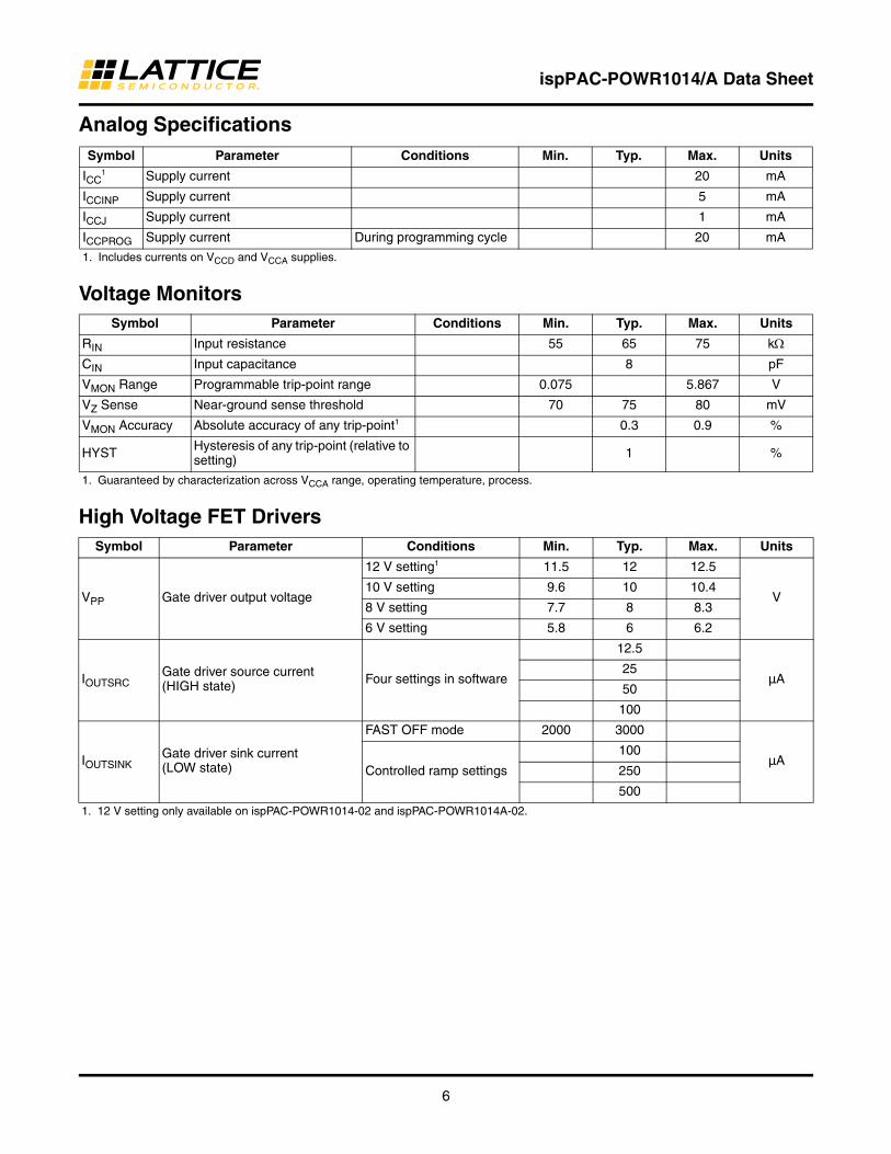
Analog Specifications
Voltage Monitors
High Voltage FET Drivers
Symbol Parameter Conditions Min. Typ. Max. Units
ICC1 Supply current 20 mA
ICCINP Supply current 5 mA
ICCJ Supply current 1 mA
ICCPROG Supply current During programming cycle 20 mA
1. Includes currents on VCCD and VCCA supplies.
Symbol Parameter Conditions Min. Typ. Max. Units
RIN Input resistance 55 65 75 k
CIN Input capacitance 8 pF
VMON Range Programmable trip-point range 0.075 5.867 V
VZ Sense Near-ground sense threshold 70 75 80 mV
VMON Accuracy Absolute accuracy of any trip-point1 0.3 0.9 %
HYST Hysteresis of any trip-point (relative to setting) 1 %
1. Guaranteed by characterization across VCCA range, operating temperature, process.
Symbol Parameter Conditions Min. Typ. Max. Units
VPP Gate driver output voltage
12 V setting1 11.5 12 12.5
V10 V setting 9.6 10 10.4
8 V setting 7.7 8 8.3
6 V setting 5.8 6 6.2
IOUTSRCGate driver source current (HIGH state) Four settings in software
12.5
µA25
50
100
IOUTSINKGate driver sink current (LOW state)
FAST OFF mode 2000 3000
µAControlled ramp settings
100
250
500
1. 12 V setting only available on ispPAC-POWR1014-02 and ispPAC-POWR1014A-02.
ispPAC-POWR1014/A Data Sheet
7
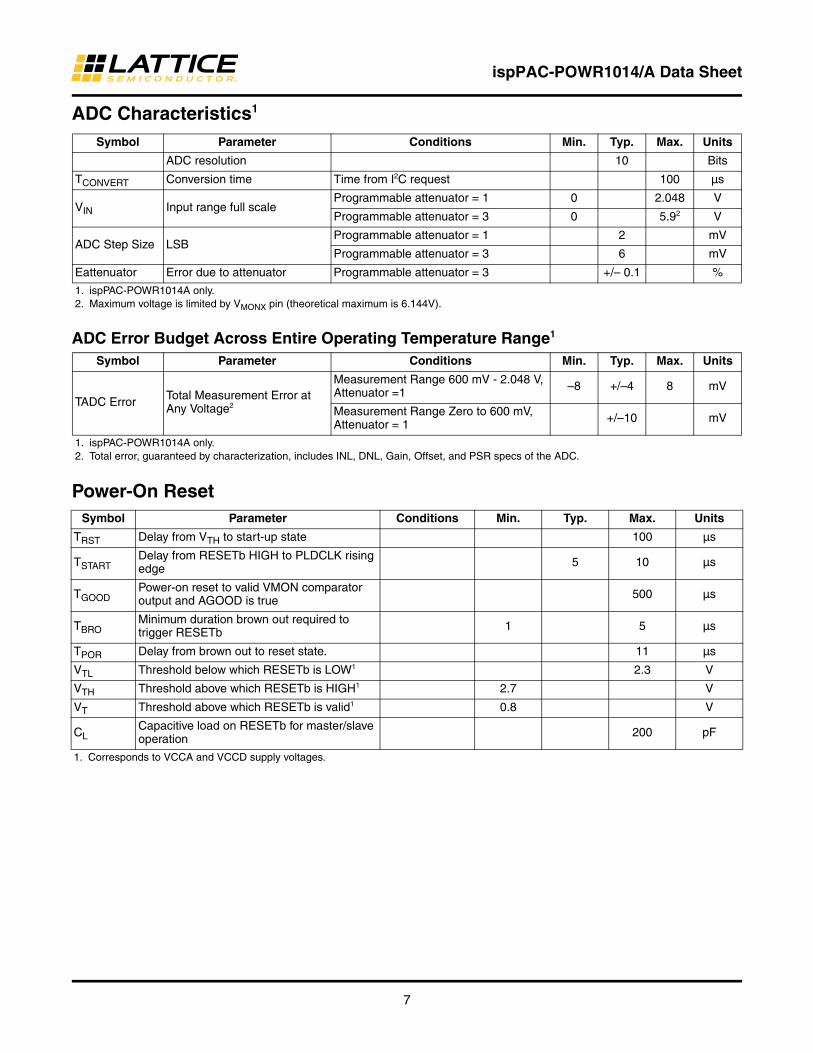
ADC Characteristics1
ADC Error Budget Across Entire Operating Temperature Range1
Power-On Reset
Symbol Parameter Conditions Min. Typ. Max. Units
ADC resolution 10 Bits
TCONVERT Conversion time Time from I2C request 100 µs
VIN Input range full scaleProgrammable attenuator = 1 0 2.048 V
Programmable attenuator = 3 0 5.92 V
ADC Step Size LSBProgrammable attenuator = 1 2 mV
Programmable attenuator = 3 6 mV
Eattenuator Error due to attenuator Programmable attenuator = 3 +/– 0.1 %
1. ispPAC-POWR1014A only.2. Maximum voltage is limited by VMONX pin (theoretical maximum is 6.144V).
Symbol Parameter Conditions Min. Typ. Max. Units
TADC Error Total Measurement Error at Any Voltage2
Measurement Range 600 mV - 2.048 V, Attenuator =1 –8 +/–4 8 mV
Measurement Range Zero to 600 mV, Attenuator = 1 +/–10 mV
1. ispPAC-POWR1014A only.2. Total error, guaranteed by characterization, includes INL, DNL, Gain, Offset, and PSR specs of the ADC.
Symbol Parameter Conditions Min. Typ. Max. Units
TRST Delay from VTH to start-up state 100 µs
TSTARTDelay from RESETb HIGH to PLDCLK rising edge 5 10 µs
TGOODPower-on reset to valid VMON comparator output and AGOOD is true 500 µs
TBROMinimum duration brown out required to trigger RESETb 1 5 µs
TPOR Delay from brown out to reset state. 11 µs
VTL Threshold below which RESETb is LOW1 2.3 V
VTH Threshold above which RESETb is HIGH1 2.7 V
VT Threshold above which RESETb is valid1 0.8 V
CLCapacitive load on RESETb for master/slave operation 200 pF
1. Corresponds to VCCA and VCCD supply voltages.

ispPAC-POWR1014/A Data Sheet
8
Figure 2. ispPAC-POWR1014/A Power-On Reset
VCC
VT
VTL
VTH
RESETb
AGOOD (Internal)
TGOOD
MCLK
PLDCLK
TBRO
TSTART
Analog Calibration
ResetState
TRST
Start UpState
TPOR
ispPAC-POWR1014/A Data Sheet
9
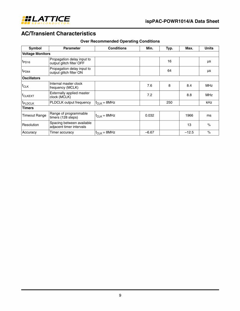
AC/Transient CharacteristicsOver Recommended Operating Conditions
Symbol Parameter Conditions Min. Typ. Max. Units
Voltage Monitors
tPD16Propagation delay input to output glitch filter OFF 16 µs
tPD64Propagation delay input to output glitch filter ON 64 µs
Oscillators
fCLKInternal master clock frequency (MCLK) 7.6 8 8.4 MHz
fCLKEXTExternally applied master clock (MCLK) 7.2 8.8 MHz
fPLDCLK PLDCLK output frequency fCLK = 8MHz 250 kHz
Timers
Timeout Range Range of programmable timers (128 steps) fCLK = 8MHz 0.032 1966 ms
Resolution Spacing between available adjacent timer intervals 13 %
Accuracy Timer accuracy fCLK = 8MHz –6.67 –12.5 %

ispPAC-POWR1014/A Data Sheet
10
Digital SpecificationsOver Recommended Operating Conditions
Symbol Parameter Conditions Min. Typ. Max. Units
IIL,IIH Input leakage, no pull-up/pull-down +/–10 µA
IOH-HVOUT Output leakage current
HVOUT[1:2] in open drain mode and pulled up to 10 V
35 60 µA
HVOUT[1:2] in open drain mode and pulled up to 13 V
35 100 µA
IPU
Input pull-up current (TMS, TDI, TDISEL, ATDI, MCLK, PLDCLK, RESETb)
70 µA
VIL Voltage input, logic low1
TDI, TMS, ATDI, TDISEL, 3.3 V supply 0.8
VTDI, TMS, ATDI, TDISEL, 2.5 V supply 0.7
SCL, SDA 30% VCCD
IN[1:4] 30% VCCINP
VIH Voltage input, logic high1
TDI, TMS, ATDI, TDISEL, 3.3 V supply 2.0
VTDI, TMS, ATDI, TDISEL, 2.5 V supply 1.7
SCL, SDA 70% VCCD VCCD
IN[1:4] 70% VCCINP VCCINP
VOL
HVOUT[1:2] (open drain mode), ISINK = 10 mA 0.8
VOUT[3:14] ISINK = 20 mA 0.8
TDO, MCLK, PLDCLK, SDA ISINK = 4 mA 0.4
VOH TDO, MCLK, PLDCLK ISRC = 4 mA VCCD - 0.4 V
ISINKTOTAL2 All digital outputs 67 mA
1. IN[1:4] referenced to VCCINP; TDO, TDI, TMS, ATDI, TDISEL referenced to VCCJ; SCL, SDA referenced to VCCD.2. Sum of maximum current sink from all digital outputs combined. Reliable operation is not guaranteed if this value is exceeded.

ispPAC-POWR1014/A Data Sheet
11
I2C Port Characteristics1
Symbol Definition
100 kHZ 400 kHZ
UnitsMin. Max. Min. Max.
FI2C I2C clock/data rate 1002 4002 kHz
TSU;STA After start 4.7 0.6 µs
THD;STA After start 4 0.6 µs
TSU;DAT Data setup 250 100 ns
TSU;STO Stop setup 4 0.6 µs
THD;DAT Data hold; SCL= Vih_min = 2.1 V 0.3 3.45 0.3 0.9 µs
TLOW Clock low period 4.7 10 1.3 10 µs
THIGH Clock high period 4 0.6 µs
TF Fall time; 2.25 V to 0.65 V 300 300 ns
TR Rise time; 0.65 V to 2.25 V 1000 300 ns
TTIMEOUT Detect clock low timeout 25 35 25 35 ms
TPOR Device must be operational after power-on reset 500 500 ms
TBUF Bus free time between stop and start condition 4.7 1.3 µs
1. Applies to ispPAC-POWR1014A only.2. If FI2C is less than 50 kHz, then the ADC DONE status bit is not guaranteed to be set after a valid conversion request is completed. In this
case, waiting for the TCONVERT minimum time after a convert request is made is the only way to guarantee a valid conversion is ready for readout. When FI2C is greater than 50 kHz, ADC conversion complete is ensured by waiting for the DONE status bit.

ispPAC-POWR1014/A Data Sheet
12
Timing for JTAG Operations
Figure 3. Erase (User Erase or Erase All) Timing Diagram
Figure 4. Programming Timing Diagram
Symbol Parameter Conditions Min. Typ. Max. Units
tISPEN Program enable delay time 10 — — µs
tISPDIS Program disable delay time 30 — — µs
tHVDIS High voltage discharge time, program 30 — — µs
tHVDIS High voltage discharge time, erase 200 — — µs
tCEN Falling edge of TCK to TDO active — — 10 ns
tCDIS Falling edge of TCK to TDO disable — — 10 ns
tSU1 Setup time 5 — — ns
tH Hold time 10 — — ns
tCKH TCK clock pulse width, high 20 — — ns
tCKL TCK clock pulse width, low 20 — — ns
fMAX Maximum TCK clock frequency — — 25 MHz
tCO Falling edge of TCK to valid output — — 10 ns
tPWV Verify pulse width 30 — — µs
tPWP Programming pulse width 20 — — ms
VIH
VIL
VIH
VIL
Update-IR Run-Test/Idle (Erase) Select-DR Scan
Clo
ck to
Shi
ft-IR
sta
te a
nd s
hift
in th
e D
isch
arge
In
stru
ctio
n, th
en c
lock
to th
e R
un-T
est/I
dle
stat
e
Run-Test/Idle (Discharge)
Specified by the Data Sheet
TMS
TCK
State
tH tH tH tH tH tH tSU1 tSU1 tSU1 tSU1 tSU1 tSU1
tSU2
tCKH tCKH tCKH tCKH tCKH tGKL tGKL
TMS
TCK
State
VIH
VIL
VIH
VI L
Update-IR Run-Test/Idle (Program) Select-DR Scan
Clo
ck to
Shi
ft-IR
sta
te a
nd s
hift
in th
e ne
xt
Inst
ruct
ion,
whi
ch w
ill s
top
the
disc
harg
e pr
oces
s
Update-IR
tSU1 tSU1 tSU1 tSU1 tSU1 tH tH tH tH tH
tCKL tPWP tCKH tCKH tCKH tCKH tCKL
ispPAC-POWR1014/A Data Sheet
13
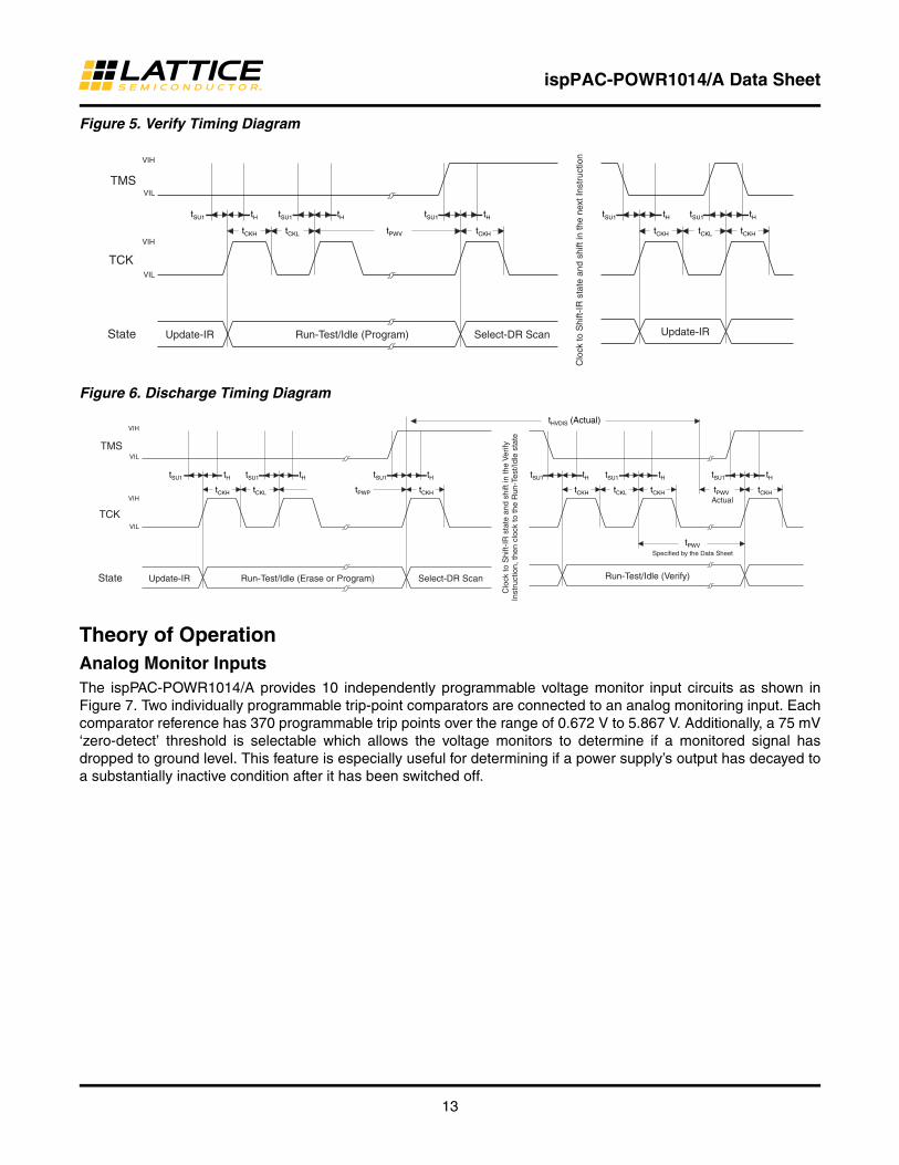
Figure 5. Verify Timing Diagram
Figure 6. Discharge Timing Diagram
Theory of OperationAnalog Monitor InputsThe ispPAC-POWR1014/A provides 10 independently programmable voltage monitor input circuits as shown in Figure 7. Two individually programmable trip-point comparators are connected to an analog monitoring input. Each comparator reference has 370 programmable trip points over the range of 0.672 V to 5.867 V. Additionally, a 75 mV ‘zero-detect’ threshold is selectable which allows the voltage monitors to determine if a monitored signal has dropped to ground level. This feature is especially useful for determining if a power supply’s output has decayed to a substantially inactive condition after it has been switched off.
TMS
TCK
State
VIH
VIL
VIH
VIL
Update-IR Run-Test/Idle (Program) Select-DR Scan
Clo
ck to
Shi
ft-IR
sta
te a
nd s
hift
in th
e ne
xt In
stru
ctio
n
Update-IR
tH tH tH tH tH
tCKH tCKH tCKH tCKL tPWV tCKH tCKL
tSU1 tSU1 tSU1 tSU1 tSU1
TMS
TCK
State
VIH
VIL
VIH
VIL
Update-IR Run-Test/Idle (Erase or Program)
Select-DR Scan
Clo
ck to
Shi
ft-IR
sta
te a
nd s
hift
in th
e V
erify
In
stru
ctio
n, th
en c
lock
to th
e R
un-T
est/I
dle
stat
e
Run-Test/Idle (Verify)
Specified by the Data Sheet
Actual
tH tH tH tH tH tH tSU1
tCKH
tHVDIS (Actual)
tCKH tCKH tCKH tCKL tPWP tPWV tCKH tCKL
tPWV
tSU1 tSU1 tSU1 tSU1 tSU1

ispPAC-POWR1014/A Data Sheet
14
Figure 7. ispPAC-POWR1014/A Voltage Monitors
Figure 7 shows the functional block diagram of one of the 10 voltage monitor inputs - ‘x’ (where x = 1...10). Each voltage monitor can be divided into three sections: Analog Input, Window Control, and Filtering.
The voltage input is monitored by two individually programmable trip-point comparators, shown as CompA and CompB. Table 1 shows all trip points and the range to which any comparator’s threshold can be set.
Each comparator outputs a HIGH signal to the PLD array if the voltage at its positive terminal is greater than its pro-grammed trip point setting, otherwise it outputs a LOW signal.
A hysteresis of approximately 1% of the setpoint is provided by the comparators to reduce false triggering as a result of input noise. The hysteresis provided by the voltage monitor is a function of the input divider setting. Table 3 lists the typical hysteresis versus voltage monitor trip-point.
AGOOD Logic SignalAll the VMON comparators auto-calibrate immediately after a power-on reset event. During this time, the digital glitch filters are also initialized. This process completion is signalled by an internally generated logic signal: AGOOD. All logic using the VMON comparator logic signals must wait for the AGOOD signal to become active.
Programmable Over-Voltage and Under-Voltage ThresholdsFigure 8 (a) shows the power supply ramp-up and ramp-down voltage waveforms. Because of hysteresis, the com-parator outputs change state at different thresholds depending on the direction of excursion of the monitored power supply.
GlitchFilter
MU
X
Trip Point A
+
–
+
–
Comp A
Comp B
Comp A/WindowSelect
VMONxB Logic Signal
VMONx
Trip Point B
Analog Input Window Control Filtering
ispPAC-POWR1014/A
To ADC(POWR1014A only)
VMONxA Logic Signal
PLDArray
VMONx Status
I2C Interface/JTAG Interface
Unit (POWR1014Aonly)
GlitchFilter

ispPAC-POWR1014/A Data Sheet
15
Figure 8. (a) Power Supply Voltage Ramp-up and Ramp-down Waveform and the Resulting Comparator Output, (b) Corresponding to Upper and Lower Trip Points
During power supply ramp-up the comparator output changes from logic 0 to 1 when the power supply voltage crosses the upper trip point (UTP). During ramp down the comparator output changes from logic state 1 to 0 when the power supply voltage crosses the lower trip point (LTP). To monitor for over-voltage fault conditions, the UTP should be used. To monitor under-voltage fault conditions, the LTP should be used.
Tables 1 and 2 show both the under-voltage and over-voltage trip points, which are automatically selected in soft-ware depending on whether the user is monitoring for an over-voltage condition or an under-voltage condition.
UTP
LTP
Mon
itore
d P
ower
Sup
ply
Vot
lage
Comparator Logic Output
(a)
(b)

ispPAC-POWR1014/A Data Sheet
16
Table 1. Trip Point Table Used For Over-Voltage Detection
Coarse Range Setting
Fine Range Setting 1 2 3 4 5 6 7 8 9 10 11 12
1 0.806 0.960 1.143 1.360 1.612 1.923 2.290 2.719 3.223 3.839 4.926 5.867
2 0.802 0.955 1.137 1.353 1.603 1.913 2.278 2.705 3.206 3.819 4.900 5.836
3 0.797 0.950 1.131 1.346 1.595 1.903 2.266 2.691 3.190 3.799 4.875 5.806
4 0.793 0.945 1.125 1.338 1.586 1.893 2.254 2.677 3.173 3.779 4.849 5.775
5 0.789 0.940 1.119 1.331 1.578 1.883 2.242 2.663 3.156 3.759 4.823 5.745
6 0.785 0.935 1.113 1.324 1.570 1.873 2.230 2.649 3.139 3.739 4.798 5.714
7 0.781 0.930 1.107 1.317 1.561 1.863 2.219 2.634 3.122 3.719 4.772 5.683
8 0.776 0.925 1.101 1.310 1.553 1.853 2.207 2.620 3.106 3.699 4.746 5.653
9 0.772 0.920 1.095 1.303 1.544 1.843 2.195 2.606 3.089 3.679 4.721 5.622
10 0.768 0.915 1.089 1.296 1.536 1.833 2.183 2.592 3.072 3.659 4.695 5.592
11 0.764 0.910 1.083 1.289 1.528 1.823 2.171 2.578 3.055 3.639 4.669 5.561
12 0.760 0.905 1.077 1.282 1.519 1.813 2.159 2.564 3.038 3.619 4.644 5.531
13 0.755 0.900 1.071 1.275 1.511 1.803 2.147 2.550 3.022 3.599 4.618 5.500
14 0.751 0.895 1.065 1.268 1.502 1.793 2.135 2.535 3.005 3.579 4.592 5.470
15 0.747 0.890 1.059 1.261 1.494 1.783 2.123 2.521 2.988 3.559 4.567 5.439
16 0.743 0.885 1.053 1.254 1.486 1.773 2.111 2.507 2.971 3.539 4.541 5.408
17 0.739 0.880 1.047 1.246 1.477 1.763 2.099 2.493 2.954 3.519 4.515 5.378
18 0.734 0.875 1.041 1.239 1.469 1.753 2.087 2.479 2.938 3.499 4.490 5.347
19 0.730 0.870 1.035 1.232 1.460 1.743 2.075 2.465 2.921 3.479 4.464 5.317
20 0.726 0.865 1.029 1.225 1.452 1.733 2.063 2.450 2.904 3.459 4.438 5.286
21 0.722 0.860 1.024 1.218 1.444 1.723 2.052 2.436 2.887 3.439 4.413 5.256
22 0.718 0.855 1.018 1.211 1.435 1.713 2.040 2.422 2.871 3.419 4.387 5.225
23 0.713 0.850 1.012 1.204 1.427 1.703 2.028 2.408 2.854 3.399 4.361 5.195
24 0.709 0.845 1.006 1.197 1.418 1.693 2.016 2.394 2.837 3.379 4.336 5.164
25 0.705 0.840 1.000 1.190 1.410 1.683 2.004 2.380 2.820 3.359 4.310 5.133
26 0.701 0.835 0.994 1.183 1.402 1.673 1.992 2.365 2.803 3.339 4.284 5.103
27 0.697 0.830 0.988 1.176 1.393 1.663 1.980 2.351 2.787 3.319 4.259 5.072
28 0.692 0.825 0.982 1.169 1.385 1.653 1.968 2.337 2.770 3.299 4.233 5.042
29 0.688 0.820 0.976 1.161 1.377 1.643 1.956 2.323 2.753 3.279 4.207 5.011
30 0.684 0.815 0.970 1.154 1.368 1.633 1.944 2.309 2.736 3.259 4.182 4.981
31 0.680 0.810 0.964 1.147 — 1.623 1.932 2.295 — 3.239 4.156 4.950
Low-V Sense 75 mV
ispPAC-POWR1014/A Data Sheet
17
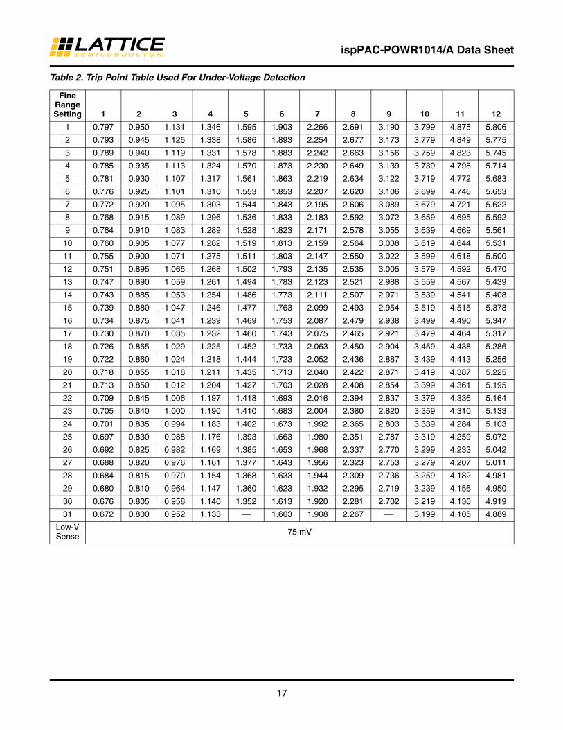
Table 2. Trip Point Table Used For Under-Voltage Detection
Fine Range Setting 1 2 3 4 5 6 7 8 9 10 11 12
1 0.797 0.950 1.131 1.346 1.595 1.903 2.266 2.691 3.190 3.799 4.875 5.806
2 0.793 0.945 1.125 1.338 1.586 1.893 2.254 2.677 3.173 3.779 4.849 5.775
3 0.789 0.940 1.119 1.331 1.578 1.883 2.242 2.663 3.156 3.759 4.823 5.745
4 0.785 0.935 1.113 1.324 1.570 1.873 2.230 2.649 3.139 3.739 4.798 5.714
5 0.781 0.930 1.107 1.317 1.561 1.863 2.219 2.634 3.122 3.719 4.772 5.683
6 0.776 0.925 1.101 1.310 1.553 1.853 2.207 2.620 3.106 3.699 4.746 5.653
7 0.772 0.920 1.095 1.303 1.544 1.843 2.195 2.606 3.089 3.679 4.721 5.622
8 0.768 0.915 1.089 1.296 1.536 1.833 2.183 2.592 3.072 3.659 4.695 5.592
9 0.764 0.910 1.083 1.289 1.528 1.823 2.171 2.578 3.055 3.639 4.669 5.561
10 0.760 0.905 1.077 1.282 1.519 1.813 2.159 2.564 3.038 3.619 4.644 5.531
11 0.755 0.900 1.071 1.275 1.511 1.803 2.147 2.550 3.022 3.599 4.618 5.500
12 0.751 0.895 1.065 1.268 1.502 1.793 2.135 2.535 3.005 3.579 4.592 5.470
13 0.747 0.890 1.059 1.261 1.494 1.783 2.123 2.521 2.988 3.559 4.567 5.439
14 0.743 0.885 1.053 1.254 1.486 1.773 2.111 2.507 2.971 3.539 4.541 5.408
15 0.739 0.880 1.047 1.246 1.477 1.763 2.099 2.493 2.954 3.519 4.515 5.378
16 0.734 0.875 1.041 1.239 1.469 1.753 2.087 2.479 2.938 3.499 4.490 5.347
17 0.730 0.870 1.035 1.232 1.460 1.743 2.075 2.465 2.921 3.479 4.464 5.317
18 0.726 0.865 1.029 1.225 1.452 1.733 2.063 2.450 2.904 3.459 4.438 5.286
19 0.722 0.860 1.024 1.218 1.444 1.723 2.052 2.436 2.887 3.439 4.413 5.256
20 0.718 0.855 1.018 1.211 1.435 1.713 2.040 2.422 2.871 3.419 4.387 5.225
21 0.713 0.850 1.012 1.204 1.427 1.703 2.028 2.408 2.854 3.399 4.361 5.195
22 0.709 0.845 1.006 1.197 1.418 1.693 2.016 2.394 2.837 3.379 4.336 5.164
23 0.705 0.840 1.000 1.190 1.410 1.683 2.004 2.380 2.820 3.359 4.310 5.133
24 0.701 0.835 0.994 1.183 1.402 1.673 1.992 2.365 2.803 3.339 4.284 5.103
25 0.697 0.830 0.988 1.176 1.393 1.663 1.980 2.351 2.787 3.319 4.259 5.072
26 0.692 0.825 0.982 1.169 1.385 1.653 1.968 2.337 2.770 3.299 4.233 5.042
27 0.688 0.820 0.976 1.161 1.377 1.643 1.956 2.323 2.753 3.279 4.207 5.011
28 0.684 0.815 0.970 1.154 1.368 1.633 1.944 2.309 2.736 3.259 4.182 4.981
29 0.680 0.810 0.964 1.147 1.360 1.623 1.932 2.295 2.719 3.239 4.156 4.950
30 0.676 0.805 0.958 1.140 1.352 1.613 1.920 2.281 2.702 3.219 4.130 4.919
31 0.672 0.800 0.952 1.133 — 1.603 1.908 2.267 — 3.199 4.105 4.889
Low-V Sense 75 mV

ispPAC-POWR1014/A Data Sheet
18
Table 3. Comparator Hysteresis vs. Trip-Point
The window control section of the voltage monitor circuit is an AND gate (with inputs: an inverted COMPA “ANDed” with COMPB signal) and a multiplexer that supports the ability to develop a ‘window’ function without using any of the PLD’s resources. Through the use of the multiplexer, voltage monitor’s ‘A’ output may be set to report either the status of the ‘A’ comparator, or the window function of both comparator outputs. The voltage monitor’s ‘A’ output indicates whether the input signal is between or outside the two comparator thresholds. Important: This windowing function is only valid in cases where the threshold of the ‘A’ comparator is set to a value higher than that of the ‘B’ comparator. Table 4 shows the operation of window function logic.
Table 4. Voltage Monitor Windowing Logic
Note that when the ‘A’ output of the voltage monitor circuit is set to windowing mode, the ‘B’ output continues to monitor the output of the ‘B’ comparator. This can be useful in that the ‘B’ output can be used to augment the win-dowing function by determining if the input is above or below the windowing range.
The third section in the ispPAC-POWR1014/A’s input voltage monitor is a digital filter. When enabled, the compara-tor output will be delayed by a filter time constant of 64 µs, and is especially useful for reducing the possibility of false triggering from noise that may be present on the voltages being monitored. When the filter is disabled, the comparator output will be delayed by 16µs. In both cases, enabled or disabled, the filters also provide synchroniza-tion of the input signals to the PLD clock. This synchronous sampling feature effectively eliminates the possibility of race conditions from occurring in any subsequent logic that is implemented in the ispPAC-POWR1014/A’s internal PLD logic.
The comparator status can be read from the I2C interface or JTAG interface (ispPAC-POWR1014A only). For details on the I2C/JTAG interfaces, please refer to the I2C/SMBUS Interface, and Accessing I2C Registers Through JTAG sections of this data sheet.
Trip-point Range (V)
Hysteresis (mV)Low Limit High Limit
0.672 0.806 8
0.800 0.960 10
0.952 1.143 12
1.133 1.360 14
1.346 1.612 17
1.603 1.923 20
1.908 2.290 24
2.267 2.719 28
2.691 3.223 34
3.199 3.839 40
4.105 4.926 51
4.889 5.867 61
75 mV 0 (Disabled)
Input Voltage Comp A Comp BWindow
(B and Not A) Comment
VIN < Trip-point B < Trip-point A 0 0 0 Outside window, low
Trip-point B < VIN < Trip-point A 0 1 1 Inside window
Trip-point B < Trip-point A < VIN 1 1 0 Outside window, high
ispPAC-POWR1014/A Data Sheet
19
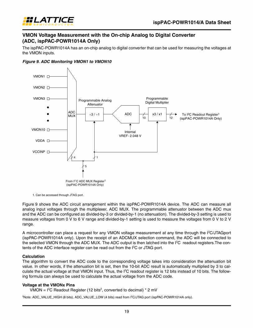
VMON Voltage Measurement with the On-chip Analog to Digital Converter (ADC, ispPAC-POWR1014A Only)The ispPAC-POWR1014A has an on-chip analog to digital converter that can be used for measuring the voltages at the VMON inputs.
Figure 9. ADC Monitoring VMON1 to VMON10
Figure 9 shows the ADC circuit arrangement within the ispPAC-POWR1014A device. The ADC can measure all analog input voltages through the multiplexer, ADC MUX. The programmable attenuator between the ADC mux and the ADC can be configured as divided-by-3 or divided-by-1 (no attenuation). The divided-by-3 setting is used to measure voltages from 0 V to 6 V range and divided-by-1 setting is used to measure the voltages from 0 V to 2 V range.
A microcontroller can place a request for any VMON voltage measurement at any time through the I2C/JTAGport (ispPAC-POWR1014A only). Upon the receipt of an ADCMUX selection command, the ADC will be connected to the selected VMON through the ADC MUX. The ADC output is then latched into the I2C readout registers.The con-tents of the ADC interface register can be read out from the I2C or JTAG port.
CalculationThe algorithm to convert the ADC code to the corresponding voltage takes into consideration the attenuation bit value. In other words, if the attenuation bit is set, then the 10-bit ADC result is automatically multiplied by 3 to cal-culate the actual voltage at that VMON input. Thus, the I2C readout register is 12 bits instead of 10 bits. The follow-ing formula can always be used to calculate the actual voltage from the ADC code.
Voltage at the VMONx PinsVMON = I2C Readout Register (12 bits2, converted to decimal) * 2 mV
2Note: ADC_VALUE_HIGH (8 bits), ADC_VALUE_LOW (4 bits) read from I2C/JTAG port (ispPAC-POWR1014A only).
VMON1
VMON2
VMON3
VMON10
VDDA
VCCINP
1. Can be accessed through JTAG port.
ADCMUX ADC
Programmable AnalogAttenuator
ProgrammableDigital Multiplier
InternalVREF- 2.048 V
4
10x3 / x1 ÷3 / ÷1
12To I2C Readout Register1
(ispPAC-POWR1014A Only)
5
From I2 C ADC MUX Register1
(ispPAC-POWR1014A Only)
1

ispPAC-POWR1014/A Data Sheet
20
PLD BlockFigure 10 shows the ispPAC-POWR1014/A PLD architecture, which is derived from the Lattice ispMACH® 4000 CPLD. The PLD architecture allows the flexibility in designing various state machines and control functions used for power supply management. The AND array has 53 inputs and generates 123 product terms. These 123 product terms are divided into three groups of 41 for each of the generic logic blocks, GLB1, GLB2, and GLB3. Each GLB is made up of eight macrocells. In total, there are 24 macrocells in the ispPAC-POWR1014/A device. The output signals of the ispPAC-POWR1014/A device are derived from GLBs as shown in Figure 10. GLB3 generates timer control.
Figure 10. ispPAC-POWR1014/A PLD Architecture
Macrocell ArchitectureThe macrocell shown in Figure 11 is the heart of the PLD. The basic macrocell has five product terms that feed the OR gate and the flip-flop. The flip-flop in each macrocell is independently configured. It can be programmed to function as a D-Type or T-Type flip-flop. Combinatorial functions are realized by bypassing the flip-flop. The polarity control and XOR gates provide additional flexibility for logic synthesis. The flip-flop’s clock is driven from the com-mon PLD clock that is generated by dividing the 8 MHz master clock by 32. The macrocell also supports asynchro-nous reset and preset functions, derived from either product terms, the global reset input, or the power-on reset signal. The resources within the macrocells share routing and contain a product term allocation array. The product term allocation array greatly expands the PLD’s ability to implement complex logical functions by allowing logic to be shared between adjacent blocks and distributing the product terms to allow for wider decode functions. All the digital inputs are registered by MCLK and the VMON comparator outputs are registered by the PLD Clock to syn-chronize them to the PLD logic.
AND Array53 Inputs123 PT
Global Reset(Resetb pin)
OutputFeedback
24
VMON[1-10]
20
IN[1:4]
Timer1Timer0
Timer2Timer3
Timer Clock
IRP18
PLD Clock
4
4
AGOOD GLB1Generic Logic Block
8 Macrocell41 PT
GLB2Generic Logic Block
8 Macrocell41 PT
GLB3Generic Logic Block
8 Macrocell41 PT
HVOUT[1..2],OUT[3..8]
OUT[9..14]
41
41
41
InputRegister
InputRegister
MCLK

ispPAC-POWR1014/A Data Sheet
21
Figure 11. ispPAC-POWR1014/A Macrocell Block Diagram
Clock and Timer FunctionsFigure 12 shows a block diagram of the ispPAC-POWR1014/A’s internal clock and timer systems. The master clock operates at a fixed frequency of 8MHz, from which a fixed 250kHz PLD clock is derived.
Figure 12. Clock and Timer System
The internal oscillator runs at a fixed frequency of 8 MHz. This signal is used as a source for the PLD and timer clocks. It is also used for clocking the comparator outputs and clocking the digital filters in the voltage monitor cir-cuits and ADC. The ispPAC-POWR1014/A can be programmed to operate in three modes: Master mode, Stand-
PT0
PT1
PT2
PT3
PT4
D/T Q
R P To PLD Output
CLK
Clock
Polarity
Macrocell flip-flop provides D, T, or combinatorial
output with polarity
Product Term Allocation
Global Reset Power On Reset
Global Polarity Fuse for Init Product Term
Block Init Product Term
Internal Oscillator
8MHz 32
Timer 0
Timer 1
Timer 3
Timer 2
MCLK PLDCLK
PLD Clock
SW0
SW1
SW2
To/From PLD

ispPAC-POWR1014/A Data Sheet
22
alone mode and Slave mode. Table 5 summarizes the operating modes of ispPAC-POWR1014/A.
Table 5. ispPAC-POWR1014/A Operating Modes
A divide-by-32 prescaler divides the internal 8 MHz oscillator (or external clock, if selected) down to 250kHz for the PLD clock and for the programmable timers. This PLD clock may be made available on the PLDCLK pin by closing SW2. Each of the four timers provides independent timeout intervals ranging from 32 µs to 1.96 seconds in 128 steps.
Digital OutputsThe ispPAC-POWR1014/A provides 14 digital outputs, HVOUT[1:2] and OUT[3:14]. Outputs OUT[3:14] are perma-nently configured as open drain to provide a high degree of flexibility when interfacing to logic signals, LEDs, opto-couplers, and power supply control inputs. The HVOUT[1:2] pins can be configured as either high voltage FET driv-ers or open drain outputs. Each of these outputs may be controlled either from the PLD or from the I2C register (isp-PAC-POWR1014A only). The determination whether a given output is under PLD or I2C control may be made on a pin-by-pin basis (see Figure 13). For further details on controlling the outputs through I2C, please see the I2C/SMBUS Interface and Accessing I2C Registers Through JTAG sections of this data sheet.
Figure 13. Digital Output Pin Configuration
High-Voltage OutputsIn addition to being usable as digital open-drain outputs, the ispPAC-POWR1014/A’s HVOUT1-HVOUT2 output pins can be programmed to operate as high-voltage FET drivers. Figure 14 shows the details of the HVOUT gate drivers. Each of these outputs may be controlled from the PLD, or with the ispPAC-POWR1014A, from the I2C reg-isters (see Figure 14). For further details on controlling the outputs through I2C, please see the I2C/SMBUS Inter-face, and Accessing I2C Registers Through JTAG sections of this data sheet.
Timer Operating Mode SW0 SW1 Condition Comments
Standalone Closed Open When only one ispPAC-POWR1014/A is used. MCLK pin tristated
Master Closed ClosedWhen more than one ispPAC-POWR1014/A is used on a board, one of them should be configured to operate in this mode.
MCLK pin outputs 8MHz clock
Slave Open Closed
When more than one ispPAC-POWR1014/As is used on a board. Other than the master, the rest of the ispPAC-POWR1014/As should be programmed as slaves.
MCLK pin is input
OUTxPin
Digital Controlfrom PLD
Digital Control from I2C Register(ispPAC-POWR1014A only)

ispPAC-POWR1014/A Data Sheet
23
Figure 14. Basic Function Diagram for an Output in High Voltage MOSFET Gate Driver Mode
Figure 14 shows the HVOUT circuitry when programmed as a FET driver. In this mode the output either sources current from a charge pump or sinks current. The maximum voltage that the output level at the pin will rise to is also programmable between 6 V and 12 V1. The maximum voltage levels that are required depend on the gate-to-source threshold of the FET being driven and the power supply voltage being switched. The maximum voltage level needs to be sufficient to bias the gate-to-source threshold on and also accommodate the load voltage at the FET’s source, since the source pin of the FET to provide a wide range of ramp rates is tied to the supply of the target board. When the HVOUT pin is sourcing current, charging a FET gate, the source current is programmable between 12.5 µA and 100 µA. When the driver is turned to the off state, the driver will sink current to ground, and this sink current is also programmable between 3000 µA and 100 µA to control the turn-off rate.
Programmable Output Voltage Levels for HVOUT1- HVOUT2There are four1 selectable steps for the output voltage of the FET drivers when in FET driver mode. The voltage that the pin is capable of driving to can be programmed from 6 V to 12 V1 in 2 V steps.
1. –01 performance grade devices provide three selectable output voltage settings from 6 V to 10 V in 2 V steps. The –02 performance grade devices also support the 12 V output voltage setting.
RESETb Signal, RESET Command via JTAG or I2CActivating the RESETb signal (Logic 0 applied to the RESETb pin) or issuing a reset instruction via JTAG, or with the ispPAC-POWR1014A, I2C will force the outputs to the following states independent of how these outputs have been configured in the PINS window:
• OUT3-14 will go high-impedance.• HVOUT pins programmed for open drain operation will go high-impedance.• HVOUT pins programmed for FET driver mode operation will pull down.
At the conclusion of the RESET event, these outputs will go to the states defined by the PINS window, and if a sequence has been programmed into the device, it will be restarted at the first step. The analog calibration will be redone and consequently, the VMONs, and ADCs will not be operational until 500 microseconds (max.) after the conclusion of the RESET event.
ISOURCE(12.5 to 100 µA)
ISINK(100 to 500 µA)+Fast Turn-off
(3000µA)
Charge Pump(6 to 12V1)
InputSupply
Load
HVOUTxPin
Digital Controlfrom PLD
1. -01 performance grade devices provide three selectable output voltage settings from 6V to 10V in 2V steps. The -02 performance grade devices also support the 12V output voltage setting.
Digital Control from I2C Register(ispPAC-POWR1014A Only)
+-

ispPAC-POWR1014/A Data Sheet
24
CAUTION: Activating the RESETb signal or issuing a RESET command through I2C or JTAG during the ispPAC-POWR1014/A device operation, results in the device aborting all operations and returning to the power-on reset state. The status of the power supplies which are being enabled by the ispPAC-POWR1014/A will be determined by the state of the outputs shown above.
I2C/SMBUS Interface (ispPAC-POWR1014A Only)I2C and SMBus are low-speed serial interface protocols designed to enable communications among a number of devices on a circuit board. The ispPAC-POWR1014A supports a 7-bit addressing of the I2C communications proto-col, as well as SMBTimeout and SMBAlert features of the SMBus, enabling it to easily integrated into many types of modern power management systems. Figure 15 shows a typical I2C configuration, in which one or more ispPAC-POWR1014As are slaved to a supervisory microcontroller. SDA is used to carry data signals, while SCL provides a synchronous clock signal. The SMBAlert line is only present in SMBus systems. The 7-bit I2C address of the POWR1014A is fully programmable through the JTAG port.
Figure 15. ispPAC-POWR1014A in I 2C/SMBUS System
In both the I2C and SMBus protocols, the bus is controlled by a single MASTER device at any given time. This mas-ter device generates the SCL clock signal and coordinates all data transfers to and from a number of slave devices. The ispPAC-POWR1014A is configured as a slave device, and cannot independently coordinate data transfers. Each slave device on a given I2C bus is assigned a unique address. The ispPAC-POWR1014A implements the 7-bit addressing portion of the standard. Any 7-bit address can be assigned to the ispPAC-POWR1014A device by pro-gramming through JTAG. When selecting a device address, one should note that several addresses are reserved by the I2C and/or SMBus standards, and should not be assigned to ispPAC-POWR1014A devices to assure bus compatibility. Table 6 lists these reserved addresses.
MICROPROCESSOR (I 2 C MASTER)
POWR1014A(I 2 C SLAVE)
POWR1014A(I 2 C SLAVE)
SDA SDA SDA SCL SCL SCL
SCL/SMCLK (CLOCK)
SDA/SMDAT (DATA)
SMBALERT
OUT3/SMBA
OUT3/SMBA
To Other I 2 C
Devices
INTERRUPT
V+
ispPAC-POWR1014/A Data Sheet
25
Table 6. I 2C/SMBus Reserved Slave Device Addresses
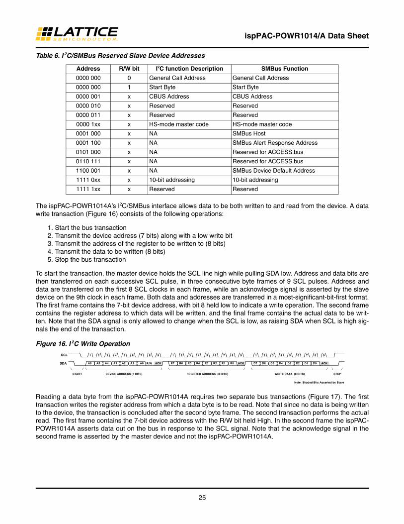
The ispPAC-POWR1014A’s I2C/SMBus interface allows data to be both written to and read from the device. A data write transaction (Figure 16) consists of the following operations:
1. Start the bus transaction 2. Transmit the device address (7 bits) along with a low write bit3. Transmit the address of the register to be written to (8 bits)4. Transmit the data to be written (8 bits)5. Stop the bus transaction
To start the transaction, the master device holds the SCL line high while pulling SDA low. Address and data bits are then transferred on each successive SCL pulse, in three consecutive byte frames of 9 SCL pulses. Address and data are transferred on the first 8 SCL clocks in each frame, while an acknowledge signal is asserted by the slave device on the 9th clock in each frame. Both data and addresses are transferred in a most-significant-bit-first format. The first frame contains the 7-bit device address, with bit 8 held low to indicate a write operation. The second frame contains the register address to which data will be written, and the final frame contains the actual data to be writ-ten. Note that the SDA signal is only allowed to change when the SCL is low, as raising SDA when SCL is high sig-nals the end of the transaction.
Figure 16. I 2C Write Operation
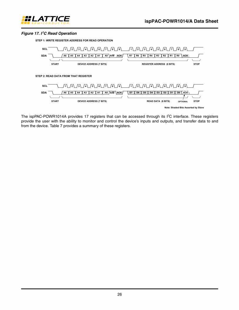
Reading a data byte from the ispPAC-POWR1014A requires two separate bus transactions (Figure 17). The first transaction writes the register address from which a data byte is to be read. Note that since no data is being written to the device, the transaction is concluded after the second byte frame. The second transaction performs the actual read. The first frame contains the 7-bit device address with the R/W bit held High. In the second frame the ispPAC-POWR1014A asserts data out on the bus in response to the SCL signal. Note that the acknowledge signal in the second frame is asserted by the master device and not the ispPAC-POWR1014A.
Address R/W bit I2C function Description SMBus Function
0000 000 0 General Call Address General Call Address
0000 000 1 Start Byte Start Byte
0000 001 x CBUS Address CBUS Address
0000 010 x Reserved Reserved
0000 011 x Reserved Reserved
0000 1xx x HS-mode master code HS-mode master code
0001 000 x NA SMBus Host
0001 100 x NA SMBus Alert Response Address
0101 000 x NA Reserved for ACCESS.bus
0110 111 x NA Reserved for ACCESS.bus
1100 001 x NA SMBus Device Default Address
1111 0xx x 10-bit addressing 10-bit addressing
1111 1xx x Reserved Reserved
ACK ACK ACK
START
1 2 3 4 5 6 7 8 9
A6 A5 A4 A3 A2 A1 A0 R7 R6 R5 R4 R3 R2 R1 R0
1 2 3 4 5 6 7 8 9 1 2 3 4 5 6 7 8 9
D7 D6 D5 D4 D3 D2 D1 D0
STOP DEVICE ADDRESS (7 BITS) REGISTER ADDRESS (8 BITS) WRITE DATA (8 BITS)
SCL
SDA R/W
Note: Shaded Bits Asserted by Slave
ispPAC-POWR1014/A Data Sheet
26
Figure 17. I 2C Read Operation
The ispPAC-POWR1014A provides 17 registers that can be accessed through its I2C interface. These registers provide the user with the ability to monitor and control the device’s inputs and outputs, and transfer data to and from the device. Table 7 provides a summary of these registers.
D5 D4 D3 D2 D1 D0 D6 D7 ACK
ACK ACK
START
1 2 3 4 5 6 7 8 9
A6 A5 A4 A3 A2 A1 A0 R7 R6 R5 R4 R3 R2 R1 R0
1 2 3 4 5 6 7 8 9
DEVICE ADDRESS (7 BITS) REGISTER ADDRESS (8 BITS)
SCL
SDA R/W
STOP
START
1 2 3 4 5 6 7 8 9
A6 A5 A4 A3 A2 A1 A0 ACK
1 2 3 4 5 6 7 8 9
DEVICE ADDRESS (7 BITS) READ DATA (8 BITS)
SCL
SDA R/W
STOP
STEP 1: WRITE REGISTER ADDRESS FOR READ OPERATION
STEP 2: READ DATA FROM THAT REGISTER
Note: Shaded Bits Asserted by Slave
OPTIONAL

ispPAC-POWR1014/A Data Sheet
27
Table 7. I 2C Control Registers1
Several registers are provided for monitoring the status of the analog inputs. The three registers VMON_STATUS[0:2] provide the ability to read the status of the VMON output comparators. The ability to read both the ‘a’ and ‘b’ comparators from each VMON input is provided through the VMON input registers. Note that if a VMON input is configured to window comparison mode, then the corresponding VMONxA register bit will reflect the status of the window comparison.
Figure 18. VMON Status Registers
It is also possible to directly read the value of the voltage present on any of the VMON inputs by using the ispPAC-POWR1014A’s ADC. Three registers provide the I2C interface to the ADC (Figure 19).
Register Address
Register Name Read/Write Description Value After POR2, 3
0x00 vmon_status0 R VMON input status Vmon[4:1] – – – – – – – –
0x01 vmon_status1 R VMON input status Vmon[8:5] – – – – – – – –
0x02 vmon_status2 R VMON input status Vmon[10:9] X X X X – – – –
0x03 output_status0 R Output status OUT[8:3], HVOUT[2:1] – – – – – – – –
0x04 output_status1 R Output status OUT[14:9] X X – – – – – –
0x06 input_status R Input status IN[4:1] X X X X – – – –
0x07 adc_value_low R ADC D[3:0] and status – – – – X X X 1
0x08 adc_value_high R ADC D[9:4] – – – – – – – –
0x09 adc_mux R/W ADC Attenuator and MUX[3:0] X X X 1 1 1 1 1
0x0A UES_byte0 R UES[7:0] – – – – – – – –
0x0B UES_byte1 R UES[15:8] – – – – – – – –
0x0C UES_byte2 R UES[23:16] – – – – – – – –
0x0D UES_byte3 R UES[31:24] – – – – – – – –
0x0E gp_output1 R/W GPOUT[8:1] 0 0 0 0 0 1 0 0
0x0F gp_output2 R/W GPOUT[14:9] X X 0 0 0 0 0 0
0x11 input_value R/W PLD Input Register [4:2] X X X X 0 0 0 X
0x12 reset W Resets device on write N/A
1. These registers can also be accessed through the JTAG interface.2. “X” = Non-functional bit (bits read out as 1’s).3. “–” = State depends on device configuration or input status.
VMON4B VMON4A VMON3B VMON3A VMON2B VMON2A VMON1B VMON1A
b7 b0
0x00 - VMON_STATUS0 (Read Only)
b6 b5 b4 b3 b2 b1
VMON8B VMON8A VMON7B VMON7A VMON6B VMON6A VMON5B VMON5A
b7 b0
0x01 - VMON_STATUS1 (Read Only)
b6 b5 b4 b3 b2 b1
VMON10B VMON10A VMON9B VMON9A1 1 1 1
b7 b0
0x02 - VMON_STATUS2 (Read Only)
b6 b5 b4 b3 b2 b1
ispPAC-POWR1014/A Data Sheet
28
Figure 19. ADC Interface Registers
To perform an A/D conversion, one must set the input attenuator and channel selector. Two input ranges may be set using the attenuator, 0 - 2.048 V and 0 - 6.144 V. Table 8 shows the input attenuator settings.
Table 8. ADC Input Attenuator Control
The input selector may be set to monitor any one of the ten VMON inputs, the VCCA input, or the VCCINP input. Table 9 shows the codes associated with each input selection.
Table 9. VMON Address Selection Table
Writing a value to the ADC_MUX register to set the input attenuator and selector will automatically initiate a conver-sion. When the conversion is in process, the DONE bit (ADC_VALUE_LOW.0) will be reset to ‘0’. When the conver-sion is complete, this bit will be set to ‘1’. When the conversion is complete, the result may be read out of the ADC by performing two I2C read operations; one for ADC_VALUE_LOW, and one for ADC_VALUE_HIGH. It is recom-mended that the I2C master load a second conversion command only after the completion of the current conversion
ATTEN (ADC_MUX.4) Resolution Full-Scale Range
0 2 mV 2.048 V
1 6 mV 6.144 V
Select Word
Input ChannelSEL3
(ADC_MUX.3)SEL2
(ADC_MUX.2)SEL1
(ADC_MUX.1)SEL0
(ADC_MUX.0)
0 0 0 0 VMON1
0 0 0 1 VMON2
0 0 1 0 VMON3
0 0 1 1 VMON4
0 1 0 0 VMON5
0 1 0 1 VMON6
0 1 1 0 VMON7
0 1 1 1 VMON8
1 0 0 0 VMON9
1 0 0 1 VMON10
1 1 0 0 VCCA
1 1 0 1 VCCINP
D3 D2 D1 D0 1 1 1 DONE
b7 b0
0x07 - ADC_VALUE_LOW (Read Only)
b6 b5 b4 b3 b2 b1
D11 D10 D9 D8 D7 D6 D5 D4
b7 b0
0x08 - ADC_VALUE_HIGH (Read Only)
b6 b5 b4 b3 b2 b1
X X X ATTEN SEL3 SEL2 SEL1 SEL0
b7 b0
0x09 - ADC_MUX (Read/Write)
b6 b5 b4 b3 b2 b1
ispPAC-POWR1014/A Data Sheet
29
command (Waiting for the DONE bit to be set to ‘1’). An alternative would be to wait for a minimum specified time (see TCONVERT value in the specifications) and disregard checking the DONE bit.
Note that if the I2C clock rate falls below 50kHz (see FI2C note in specifications), the only way to insure a valid ADC conversion is to wait the minimum specified time (TCONVERT), as the operation of the DONE bit at clock rates lower than that cannot be guaranteed. In other words, if the I2C clock rate is less than 50kHz, the DONE bit may or may not assert even though a valid conversion result is available.
To insure every ADC conversion result is valid, preferred operation is to clock I2C at more than 50kHz and verify DONE bit status or wait for the full TCONVERT time period between subsequent ADC convert commands. If an I2C request is placed before the current conversion is complete, the DONE bit will be set to 1 only after the second request is complete.
The status of the digital input lines may also be monitored and controlled through I2C commands. Figure 20 shows the I2C interface to the IN[1:4] digital input lines. The input status may be monitored by reading the INPUT_STATUS register, while input values to the PLD array may be set by writing to the INPUT_VALUE register. To be able to set an input value for the PLD array, the input multiplexer associated with that bit needs to be set to the I2C register set-ting in E2CMOS memory otherwise the PLD will receive its input from the INx pin.
Figure 20. I 2C Digital Input Interface
The digital outputs may also be monitored and controlled through the I2C interface, as shown in Figure 21. The sta-tus of any given digital output may be read by reading the contents of the associated OUTPUT_STATUS[1:0] regis-ter. Note that in the case of the outputs, the status reflected by these registers reflects the logic signal used to drive the pin, and does not sample the actual level present on the output pin. For example, if an output is set high but is
Input_Status Input_Value
3
3
3
PLD Array
I2C Interface Unit
IN[2..4]
IN1
USERJTAG Bit
2
3
PLD Output/Input_Value Register Select (E2 Configuration)
IN4 IN3 IN2 IN11 1 1 1
b7 b0
0x06 - INPUT_STATUS (Read Only)
b6 b5 b4 b3 b2 b1
X X XX
b7 b0
0x11 - INPUT_VALUE (Read/Write)
b6 b5 b4 b3 b2 b1
MUX
MUX
I4 I3 I2 X
ispPAC-POWR1014/A Data Sheet
30
not pulled up, the output status bit corresponding with that pin will read ‘1’, but a high output signal will not appear on the pin.
Digital outputs may also be optionally controlled directly by the I2C bus instead of by the PLD array. The outputs may be driven either from the PLD output or from the contents of the GP_OUTPUT[1:0] registers with the choice user-settable in E2CMOS memory. Each output may be independently set to output from the PLD or from the GP_OUTPUT registers.
Figure 21. I 2C Output Monitor and Control Logic
The UES word may also be read through the I2C interface, with the register mapping shown in Figure 22.
Output_Status0 Output_Status1
GP_Output1 GP_Output2
14
14
HVOUT[1..2]OUT[3..14]
I2C Interface Unit
PLD Output/GP_Output Register Select(E2 Configuration)
OUT8 OUT7 OUT6 OUT5 HVOUT2 HVOUT1OUT4
1 1
OUT3
b7 b0
0x03 - OUTPUT_STATUS0 (Read Only)
b6 b5 b4 b3 b2 b1
OUT14 OUT13 OUT12 OUT11 OUT10 OUT9
b7 b0
0x04 - OUTPUT_STATUS1 (Read Only)
b6 b5 b4 b3 b2 b1
GP8 GP7 GP6 GP5 GP4 GP3_ENb GP2 GP1
b7 b0
0x0E - GP_OUTPUT1 (Read/Write)
b6 b5 b4 b3 b2 b1
X X GP14 GP13 GP12 GP11 GP10 GP9
b7 b0
0x0F - GP_OUTPUT2 (Read/Write)
b6 b5 b4 b3 b2 b1
14
14
14
MUX
PLDOutputRouting
Pool
ispPAC-POWR1014/A Data Sheet
31
Figure 22. I 2C Register Mapping for UES Bits
The I2C interface also provides the ability to initiate reset operations. The ispPAC-POWR1014A may be reset by issuing a write of any value to the I2C RESET register (Figure 23). Note: The execution of the I2C reset command is equivalent to toggling the Resetb pin of the chip. Refer to the Resetb Signal, RESET Command via JTAG or I2C section of this data sheet for further information.
Figure 23. I 2C Reset Register
UES7 UES6 UES5 UES4 UES3 UES2 UES1 UES0
b7 b0
0x0A - UES_BYTE0 (Read Only)
b6 b5 b4 b3 b2 b1
UES15 UES14 UES13 UES12 UES11 UES10 UES9 UES8
b7 b0
0x0B - UES_BYTE1 (Read Only)
b6 b5 b4 b3 b2 b1
UES23 UES22 UES21 UES20 UES19 UES18 UES17 UES16
b7 b0
0x0C - UES_BYTE2 (Read Only)
b6 b5 b4 b3 b2 b1
UES31 UES30 UES29 UES28 UES27 UES26 UES25 UES24
b7 b0
0x0D - UES_BYTE3 (Read Only)
b6 b5 b4 b3 b2 b1
X X X X X X X X
b7 b0
0x12 - RESET (Write Only)
b6 b5 b4 b3 b2 b1

ispPAC-POWR1014/A Data Sheet
32
SMBus SMBAlert FunctionThe ispPAC-POWR1014A provides an SMBus SMBAlert function so that it can request service from the bus mas-ter when it is used as part of an SMBus system. This feature is supported as an alternate function of OUT3. When the SMBAlert feature is enabled, OUT3 is controlled by a combination of the PLD output and the GP3_ENb bit (Figure 24). Note: To enable the SMBAlert feature, the SMB_Mode (EECMOS bit) should be set in software.
Figure 24. ispPAC-POWR1014/A SMBAlert Logic
The typical flow for an SMBAlert transaction is as follows (Figure 24):
1. GP3_ENb bit is forced (Via I2C write) to Low2. ispPAC-POWR1014A PLD Logic pulls OUT3/SMBA Low3. Master responds to interrupt from SMBA line4. Master broadcasts a read operation using the SMBus Alert Response Address (ARA)5. ispPAC-POWR1014A responds to read request by transmitting its device address6. If transmitted device address matches ispPAC-POWR1014A address, it sets GP3_ENb bit high.
This releases OUT3/SMBA.
Figure 25. SMBAlert Bus Transaction
After OUT3/SMBA has been released, the bus master (typically a microcontroller) may opt to perform some service functions in which it may send data to or read data from the ispPAC-POWR1014A. As part of the service functions, the bus master will typically need to clear whatever condition initiated the SMBAlert request, and will also need to reset GP3_ENb to re-enable the SMBAlert function. For further information on the SMBus, the user should consult the SMBus Standard.
PLDOutputRouting
Pool MUXMUX
GP3_ENb
SMBAlertLogic
OUT3/SMBA
I2C Interface Unit
PLD Output/GP_Output Register Select (E2 Configuration)
OUT3/SMBA Mode Select(E2 Configuration)
ACK A4 A3 A2 A1 A0 x A5 A6
START
1 2 3 4 5 6 7 8 9
0 0 0 1 1 0 0 ACK
1 2 3 4 5 6 7 8 9
ALERT RESPONSE ADDRESS (0001 100)
SLAVE ADDRESS (7 BITS)
SCL
SDA R/W
STOP
SMBA
Note: Shaded Bits Asserted by Slave
SLAVE ASSERTS
SMBA
SLAVE RELEASES
SMBA

ispPAC-POWR1014/A Data Sheet
33
Software-Based Design EnvironmentDesigners can configure the ispPAC-POWR1014/A using PAC-Designer, an easy to use, Microsoft Windows com-patible program. Circuit designs are entered graphically and then verified, all within the PAC-Designer environment. Full device programming is supported using PC parallel port I/O operations and a download cable connected to the serial programming interface pins of the ispPAC-POWR1014/A. A library of configurations is included with basic solutions and examples of advanced circuit techniques are available on the Lattice web site for downloading. In addition, comprehensive online and printed documentation is provided that covers all aspects of PAC-Designer operation. The PAC-Designer schematic window, shown in Figure 26, provides access to all configurable ispPAC-POWR1014/A elements via its graphical user interface. All analog input and output pins are represented. Static or non-configurable pins such as power, ground, and the serial digital interface are omitted for clarity. Any element in the schematic window can be accessed via mouse operations as well as menu commands. When completed, con-figurations can be saved, simulated, and downloaded to devices.
Figure 26. PAC-Designer ispPAC-POWR1014/A Design Entry Screen
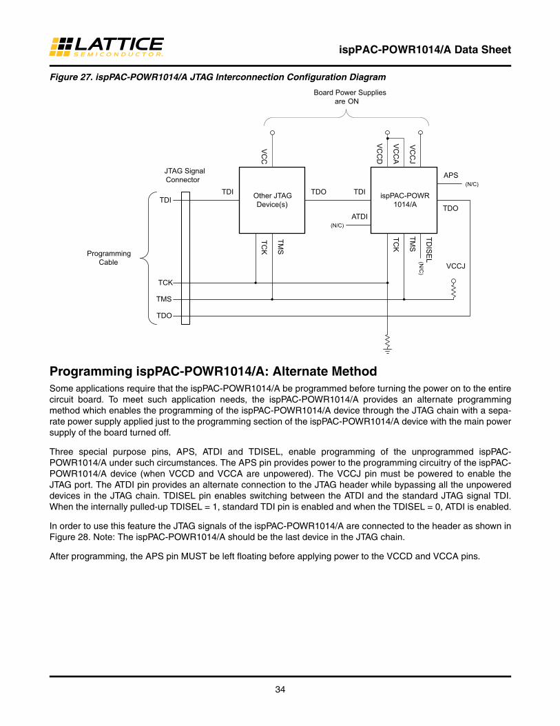
In-System ProgrammingThe ispPAC-POWR1014/A is an in-system programmable device. This is accomplished by integrating all E2 config-uration memory and control logic on-chip. Programming is performed through a 4-wire, IEEE 1149.1 compliant serial JTAG interface at normal logic levels (see Figure 27). Once a device is programmed, all configuration infor-mation is stored on-chip, in non-volatile E2CMOS memory cells. The specifics of the IEEE 1149.1 serial interface and all ispPAC-POWR1014/A instructions are described in the JTAG interface section of this data sheet.
ispPAC-POWR1014/A Data Sheet
34
Figure 27. ispPAC-POWR1014/A JTAG Interconnection Configuration Diagram
Programming ispPAC-POWR1014/A: Alternate Method Some applications require that the ispPAC-POWR1014/A be programmed before turning the power on to the entire circuit board. To meet such application needs, the ispPAC-POWR1014/A provides an alternate programming method which enables the programming of the ispPAC-POWR1014/A device through the JTAG chain with a sepa-rate power supply applied just to the programming section of the ispPAC-POWR1014/A device with the main power supply of the board turned off.
Three special purpose pins, APS, ATDI and TDISEL, enable programming of the unprogrammed ispPAC-POWR1014/A under such circumstances. The APS pin provides power to the programming circuitry of the ispPAC-POWR1014/A device (when VCCD and VCCA are unpowered). The VCCJ pin must be powered to enable the JTAG port. The ATDI pin provides an alternate connection to the JTAG header while bypassing all the unpowered devices in the JTAG chain. TDISEL pin enables switching between the ATDI and the standard JTAG signal TDI. When the internally pulled-up TDISEL = 1, standard TDI pin is enabled and when the TDISEL = 0, ATDI is enabled.
In order to use this feature the JTAG signals of the ispPAC-POWR1014/A are connected to the header as shown in Figure 28. Note: The ispPAC-POWR1014/A should be the last device in the JTAG chain.
After programming, the APS pin MUST be left floating before applying power to the VCCD and VCCA pins.
ispPAC-POWR1014/A
Other JTAGDevice(s)
TDO TDI
TDO
TDITDI
TDO
TCK
ATDI
TCK
TMS
TMS
TDIS
EL
APS(N/C)
TMS
TCK
JTAG SignalConnector
VC
CD
VC
CA
VC
CJ
VCCJ
VC
C
Board Power Suppliesare ON
(N/C
)
ProgrammingCable
(N/C)

ispPAC-POWR1014/A Data Sheet
35
Figure 28. ispPAC-POWR1014/A Alternate Configuration Diagram
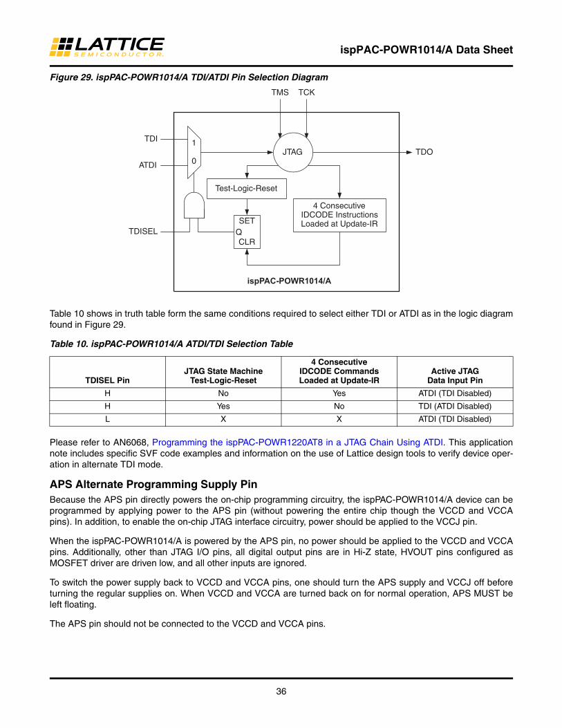
Alternate TDI Selection Via JTAG CommandWhen the TDISEL pin held high and four consecutive IDCODE instructions are issued, ispPAC-POWR1014/A responds by making its active JTAG data input the ATDI pin. When ATDI is selected, data on its TDI pin is ignored until the JTAG state machine returns to the Test-Logic-Reset state.
This method of selecting ATDI takes advantage of the fact that a JTAG device with an IDCODE register will auto-matically load its unique IDCODE instruction into the Instruction Register after a Test-Logic-Reset. This JTAG capability permits blind interrogation of devices so that their location in a serial chain can be identified without hav-ing to know anything about them in advance. A blind interrogation can be made using only the TMS and TCLK con-trol pins, which means TDI and TDO are not required for performing the operation. Figure 29 illustrates the logic for selecting whether the TDI or ATDI pin is the active data input to ispPAC-POWR1014/A.
ispPAC-POWR1014/A
Other JTAGDevice(s)
TDO TDI
TDO
TDITDI
TDO
TCK
ATDI
TCK
TMS
TMS
TDIS
EL
APS
TDISEL
TMS
TCK
JTAG SignalConnector
VC
CD
VC
CA
VC
CJ
VCCJ
VC
C
Board Power Suppliesare OFF
APS(off board Power Supply)
ProgrammingCable
D1 D2
ispPAC-POWR1014/A Data Sheet
36
Figure 29. ispPAC-POWR1014/A TDI/ATDI Pin Selection Diagram
Table 10 shows in truth table form the same conditions required to select either TDI or ATDI as in the logic diagram found in Figure 29.
Table 10. ispPAC-POWR1014/A ATDI/TDI Selection Table
Please refer to AN6068, Programming the ispPAC-POWR1220AT8 in a JTAG Chain Using ATDI. This application note includes specific SVF code examples and information on the use of Lattice design tools to verify device oper-ation in alternate TDI mode.
APS Alternate Programming Supply PinBecause the APS pin directly powers the on-chip programming circuitry, the ispPAC-POWR1014/A device can be programmed by applying power to the APS pin (without powering the entire chip though the VCCD and VCCA pins). In addition, to enable the on-chip JTAG interface circuitry, power should be applied to the VCCJ pin.
When the ispPAC-POWR1014/A is powered by the APS pin, no power should be applied to the VCCD and VCCA pins. Additionally, other than JTAG I/O pins, all digital output pins are in Hi-Z state, HVOUT pins configured as MOSFET driver are driven low, and all other inputs are ignored.
To switch the power supply back to VCCD and VCCA pins, one should turn the APS supply and VCCJ off before turning the regular supplies on. When VCCD and VCCA are turned back on for normal operation, APS MUST be left floating.
The APS pin should not be connected to the VCCD and VCCA pins.
TDISEL PinJTAG State Machine
Test-Logic-Reset
4 Consecutive IDCODE Commands Loaded at Update-IR
Active JTAG Data Input Pin
H No Yes ATDI (TDI Disabled)
H Yes No TDI (ATDI Disabled)
L X X ATDI (TDI Disabled)
1
0
TDI
ATDI
TDISEL QSET
CLR
Test-Logic-Reset
4 ConsecutiveIDCODE InstructionsLoaded at Update-IR
TDO
TMS TCK
JTAG
ispPAC-POWR1014/A
ispPAC-POWR1014/A Data Sheet
37
User Electronic SignatureA user electronic signature (UES) feature is included in the E2CMOS memory of the ispPAC-POWR1014/A. This consists of 32 bits that can be configured by the user to store unique data such as ID codes, revision numbers or inventory control data. The specifics of this feature are discussed in the IEEE 1149.1 serial interface section of this data sheet.
Electronic SecurityAn electronic security “fuse” (ESF) bit is provided in every ispPAC-POWR1014/A device to prevent unauthorized readout of the E2CMOS configuration bit patterns. Once programmed, this cell prevents further access to the func-tional user bits in the device. This cell can only be erased by reprogramming the device, so the original configura-tion cannot be examined once programmed. Usage of this feature is optional. The specifics of this feature are discussed in the IEEE 1149.1 serial interface section of this data sheet.
Production Programming SupportOnce a final configuration is determined, an ASCII format JEDEC file can be created using the PAC-Designer soft-ware. Devices can then be ordered through the usual supply channels with the user’s specific configuration already preloaded into the devices. By virtue of its standard interface, compatibility is maintained with existing production programming equipment, giving customers a wide degree of freedom and flexibility in production planning.
Evaluation FixtureBecause the features of an ispPAC-POWR1014/A are all included in the larger ispPAC-POWR1220AT8 device, designs implemented in an ispPAC-POWR1014/A can be verified using an ispPAC-POWR1220AT8 engineering prototype board connected to the parallel port of a PC with a Lattice ispDOWNLOAD™ cable. The board demon-strates proper layout techniques and can be used in real time to check circuit operation as part of the design pro-cess. Input and output connections are provided to aid in the evaluation of the functionality implemented in ispPAC-POWR1014/A for a given application. (Figure 30).
Figure 30. Download from a PC
IEEE Standard 1149.1 Interface (JTAG)Serial Port Programming Interface Communication with the ispPAC-POWR1014/A is facilitated via an IEEE 1149.1 test access port (TAP). It is used by the ispPAC-POWR1014/A as a serial programming interface. A brief descrip-tion of the ispPAC-POWR1014/A JTAG interface follows. For complete details of the reference specification, refer to the publication, Standard Test Access Port and Boundary-Scan Architecture, IEEE Std 1149.1-1990 (which now includes IEEE Std 1149.1a-1993).
OverviewAn IEEE 1149.1 test access port (TAP) provides the control interface for serially accessing the digital I/O of the isp-PAC-POWR1014/A. The TAP controller is a state machine driven with mode and clock inputs. Given in the correct sequence, instructions are shifted into an instruction register, which then determines subsequent data input, data
ispDOWNLOAD Cable (6')
4
OtherSystemCircuitry
ispPAC-POWR1220AT8Device
PAC-Designer Software

ispPAC-POWR1014/A Data Sheet
38
output, and related operations. Device programming is performed by addressing the configuration register, shifting data in, and then executing a program configuration instruction, after which the data is transferred to internal E2CMOS cells. It is these non-volatile cells that store the configuration or the ispPAC-POWR1014/A. A set of instructions are defined that access all data registers and perform other internal control operations. For compatibil-ity between compliant devices, two data registers are mandated by the IEEE 1149.1 specification. Others are func-tionally specified, but inclusion is strictly optional. Finally, there are provisions for optional data registers defined by the manufacturer. The two required registers are the bypass and boundary-scan registers. Figure 31 shows how the instruction and various data registers are organized in an ispPAC-POWR1014/A.
Figure 31. ispPAC-POWR1014/A TAP Registers
TAP Controller SpecificsThe TAP is controlled by the Test Clock (TCK) and Test Mode Select (TMS) inputs. These inputs determine whether an Instruction Register or Data Register operation is performed. Driven by the TCK input, the TAP consists of a small 16-state controller design. In a given state, the controller responds according to the level on the TMS input as shown in Figure 32. Test Data In (TDI) and TMS are latched on the rising edge of TCK, with Test Data Out (TDO) becoming valid on the falling edge of TCK. There are six steady states within the controller: Test-Logic-Reset, Run- Test/Idle, Shift-Data-Register, Pause-Data-Register, Shift-Instruction-Register and Pause-Instruction-Register. But there is only one steady state for the condition when TMS is set high: the Test-Logic-Reset state. This allows a reset of the test logic within five TCKs or less by keeping the TMS input high. Test-Logic-Reset is the power-on default state.
ADDRESS REGISTER (109 BITS)
E2CMOSNON-VOLATILE
MEMORY
UES REGISTER (32 BITS)
IDCODE REGISTER (32 BITS)
BYPASS REGISTER (1 BIT)
INSTRUCTION REGISTER (8 BITS)
TEST ACCESS PORT (TAP)LOGIC
OUTPUTLATCH
TDI TCK TMS TDO
CFG ADDRESS REGISTER (12 BITS)
MU
LTIP
LEX
ER
DATA REGISTER (123 BITS)
CFG DATA REGISTER (56 BITS)
I2C CONTROL REGISTER (12 BITS)
I2C DATA REGISTER (72 BITS)
ispPAC-POWR1014/A Data Sheet
39
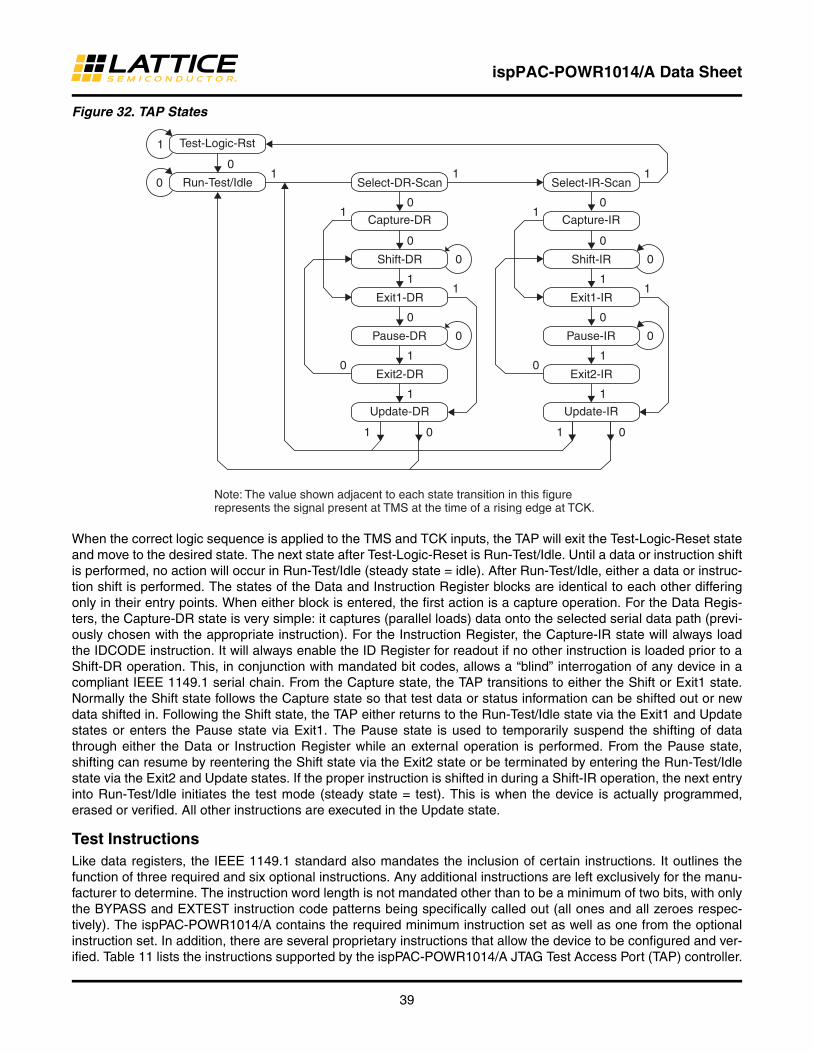
Figure 32. TAP States
When the correct logic sequence is applied to the TMS and TCK inputs, the TAP will exit the Test-Logic-Reset state and move to the desired state. The next state after Test-Logic-Reset is Run-Test/Idle. Until a data or instruction shift is performed, no action will occur in Run-Test/Idle (steady state = idle). After Run-Test/Idle, either a data or instruc-tion shift is performed. The states of the Data and Instruction Register blocks are identical to each other differing only in their entry points. When either block is entered, the first action is a capture operation. For the Data Regis-ters, the Capture-DR state is very simple: it captures (parallel loads) data onto the selected serial data path (previ-ously chosen with the appropriate instruction). For the Instruction Register, the Capture-IR state will always load the IDCODE instruction. It will always enable the ID Register for readout if no other instruction is loaded prior to a Shift-DR operation. This, in conjunction with mandated bit codes, allows a “blind” interrogation of any device in a compliant IEEE 1149.1 serial chain. From the Capture state, the TAP transitions to either the Shift or Exit1 state. Normally the Shift state follows the Capture state so that test data or status information can be shifted out or new data shifted in. Following the Shift state, the TAP either returns to the Run-Test/Idle state via the Exit1 and Update states or enters the Pause state via Exit1. The Pause state is used to temporarily suspend the shifting of data through either the Data or Instruction Register while an external operation is performed. From the Pause state, shifting can resume by reentering the Shift state via the Exit2 state or be terminated by entering the Run-Test/Idle state via the Exit2 and Update states. If the proper instruction is shifted in during a Shift-IR operation, the next entry into Run-Test/Idle initiates the test mode (steady state = test). This is when the device is actually programmed, erased or verified. All other instructions are executed in the Update state.
Test InstructionsLike data registers, the IEEE 1149.1 standard also mandates the inclusion of certain instructions. It outlines the function of three required and six optional instructions. Any additional instructions are left exclusively for the manu-facturer to determine. The instruction word length is not mandated other than to be a minimum of two bits, with only the BYPASS and EXTEST instruction code patterns being specifically called out (all ones and all zeroes respec-tively). The ispPAC-POWR1014/A contains the required minimum instruction set as well as one from the optional instruction set. In addition, there are several proprietary instructions that allow the device to be configured and ver-ified. Table 11 lists the instructions supported by the ispPAC-POWR1014/A JTAG Test Access Port (TAP) controller.
Test-Logic-Rst
Run-Test/Idle Select-DR-Scan Select-IR-Scan
Capture-DR Capture-IR
Shift-DR Shift-IR
Exit1-DR Exit1-IR
Pause-DR Pause-IR
Exit2-DR Exit2-IR
Update-DR Update-IR
1
0
0 0
0 0
0 0
1 1
0 0
0 0
1 1
1 1
0 0 1 1
0 0
1 1
1 1
1 1 1 0
Note: The value shown adjacent to each state transition in this figure represents the signal present at TMS at the time of a rising edge at TCK.
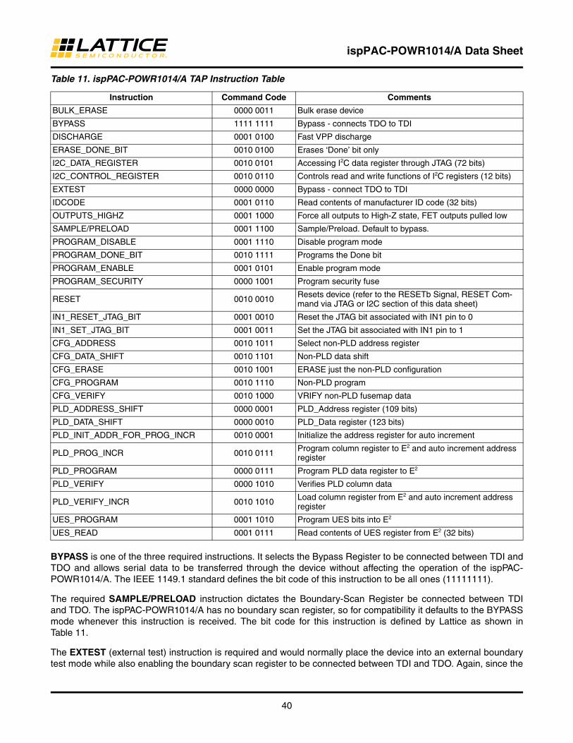
ispPAC-POWR1014/A Data Sheet
40
Table 11. ispPAC-POWR1014/A TAP Instruction Table
BYPASS is one of the three required instructions. It selects the Bypass Register to be connected between TDI and TDO and allows serial data to be transferred through the device without affecting the operation of the ispPAC-POWR1014/A. The IEEE 1149.1 standard defines the bit code of this instruction to be all ones (11111111).
The required SAMPLE/PRELOAD instruction dictates the Boundary-Scan Register be connected between TDI and TDO. The ispPAC-POWR1014/A has no boundary scan register, so for compatibility it defaults to the BYPASS mode whenever this instruction is received. The bit code for this instruction is defined by Lattice as shown in Table 11.
The EXTEST (external test) instruction is required and would normally place the device into an external boundary test mode while also enabling the boundary scan register to be connected between TDI and TDO. Again, since the
Instruction Command Code Comments
BULK_ERASE 0000 0011 Bulk erase device
BYPASS 1111 1111 Bypass - connects TDO to TDI
DISCHARGE 0001 0100 Fast VPP discharge
ERASE_DONE_BIT 0010 0100 Erases ‘Done’ bit only
I2C_DATA_REGISTER 0010 0101 Accessing I2C data register through JTAG (72 bits)
I2C_CONTROL_REGISTER 0010 0110 Controls read and write functions of I2C registers (12 bits)
EXTEST 0000 0000 Bypass - connect TDO to TDI
IDCODE 0001 0110 Read contents of manufacturer ID code (32 bits)
OUTPUTS_HIGHZ 0001 1000 Force all outputs to High-Z state, FET outputs pulled low
SAMPLE/PRELOAD 0001 1100 Sample/Preload. Default to bypass.
PROGRAM_DISABLE 0001 1110 Disable program mode
PROGRAM_DONE_BIT 0010 1111 Programs the Done bit
PROGRAM_ENABLE 0001 0101 Enable program mode
PROGRAM_SECURITY 0000 1001 Program security fuse
RESET 0010 0010 Resets device (refer to the RESETb Signal, RESET Com-mand via JTAG or I2C section of this data sheet)
IN1_RESET_JTAG_BIT 0001 0010 Reset the JTAG bit associated with IN1 pin to 0
IN1_SET_JTAG_BIT 0001 0011 Set the JTAG bit associated with IN1 pin to 1
CFG_ADDRESS 0010 1011 Select non-PLD address register
CFG_DATA_SHIFT 0010 1101 Non-PLD data shift
CFG_ERASE 0010 1001 ERASE just the non-PLD configuration
CFG_PROGRAM 0010 1110 Non-PLD program
CFG_VERIFY 0010 1000 VRIFY non-PLD fusemap data
PLD_ADDRESS_SHIFT 0000 0001 PLD_Address register (109 bits)
PLD_DATA_SHIFT 0000 0010 PLD_Data register (123 bits)
PLD_INIT_ADDR_FOR_PROG_INCR 0010 0001 Initialize the address register for auto increment
PLD_PROG_INCR 0010 0111 Program column register to E2 and auto increment address register
PLD_PROGRAM 0000 0111 Program PLD data register to E2
PLD_VERIFY 0000 1010 Verifies PLD column data
PLD_VERIFY_INCR 0010 1010 Load column register from E2 and auto increment address register
UES_PROGRAM 0001 1010 Program UES bits into E2
UES_READ 0001 0111 Read contents of UES register from E2 (32 bits)

ispPAC-POWR1014/A Data Sheet
41
ispPAC-POWR1014/A has no boundary scan logic, the device is put in the BYPASS mode to ensure specification compatibility. The bit code of this instruction is defined by the 1149.1 standard to be all zeros (00000000).
The optional IDCODE (identification code) instruction is incorporated in the ispPAC-POWR1014/A and leaves it in its functional mode when executed. It selects the Device Identification Register to be connected between TDI and TDO. The Identification Register is a 32-bit shift register containing information regarding the IC manufacturer, device type and version code (Figure 33). Access to the Identification Register is immediately available, via a TAP data scan operation, after power-up of the device, or by issuing a Test-Logic-Reset instruction. The bit code for this instruction is defined by Lattice as shown in Table 11.
Figure 33. ispPAC-POWR1014/A ID Code
ispPAC-POWR1014/A Specific InstructionsThere are 25 unique instructions specified by Lattice for the ispPAC-POWR1014/A. These instructions are primarily used to interface to the various user registers and the E2CMOS non-volatile memory. Additional instructions are used to control or monitor other features of the device. A brief description of each unique instruction is provided in detail below, and the bit codes are found in Table 11.
PLD_ADDRESS_SHIFT – This instruction is used to set the address of the PLD AND/ARCH arrays for subsequent program or read operations. This instruction also forces the outputs into the OUTPUTS_HIGHZ.
PLD_DATA_SHIFT – This instruction is used to shift PLD data into the register prior to programming or reading. This instruction also forces the outputs into the OUTPUTS_HIGHZ.
PLD_INIT_ADDR_FOR_PROG_INCR – This instruction prepares the PLD address register for subsequent PLD_PROG_INCR or PLD_VERIFY_INCR instructions.
PLD_PROG_INCR – This instruction programs the PLD data register for the current address and increments the address register for the next set of data.
PLD_PROGRAM – This instruction programs the selected PLD AND/ARCH array column. The specific column is preselected by using PLD_ADDRESS_SHIFT instruction. The programming occurs at the second rising edge of the TCK in Run-Test-Idle JTAG state. The device must already be in programming mode (PROGRAM_ENABLE instruction). This instruction also forces the outputs into the OUTPUTS_HIGHZ.
PROGRAM_SECURITY – This instruction is used to program the electronic security fuse (ESF) bit. Programming the ESF bit protects proprietary designs from being read out. The programming occurs at the second rising edge of the TCK in Run-Test-Idle JTAG state. The device must already be in programming mode (PROGRAM_ENABLE instruction). This instruction also forces the outputs into the OUTPUTS_HIGHZ.
0000 0000 0001 0100 0101 / 0000 0100 001 / 1 (ispPAC-POWR1014A-1)
0001 0000 0001 0100 0101 / 0000 0100 001 / 1 (ispPAC-POWR1014-1)
0010 0000 0001 0100 0101 / 0000 0100 001 / 1 (ispPAC-POWR1014A-2)
0011 0000 0001 0100 0101 / 0000 0100 001 / 1 (ispPAC-POWR1014-2)
MSB LSB
Part Number(20 bits)
00145h = ispPAC-POWR1014A-110145h = ispPAC-POWR1014-120145h = ispPAC-POWR1014A-230145h = ispPAC-POWR1014-2
JEDEC ManufacturerIdentity Code for
Lattice Semiconductor(11 bits) Constant 1
(1 bit)per 1149.1-1990

ispPAC-POWR1014/A Data Sheet
42
PLD_VERIFY – This instruction is used to read the content of the selected PLD AND/ARCH array column. This specific column is preselected by using PLD_ADDRESS_SHIFT instruction. This instruction also forces the outputs into the OUTPUTS_HIGHZ.
DISCHARGE – This instruction is used to discharge the internal programming supply voltage after an erase or pro-gramming cycle and prepares ispPAC-POWR1014/A for a read cycle. This instruction also forces the outputs into the OUTPUTS_HIGHZ.
CFG_ADDRESS – This instruction is used to set the address of the CFG array for subsequent program or read operations. This instruction also forces the outputs into the OUTPUTS_HIGHZ.
CFG_DATA_SHIFT – This instruction is used to shift data into the CFG register prior to programming or reading. This instruction also forces the outputs into the OUTPUTS_HIGHZ.
CFG_ERASE – This instruction will bulk erase the CFG array. The action occurs at the second rising edge of TCK in Run-Test-Idle JTAG state. The device must already be in programming mode (PROGRAM_ENABLE instruction). This instruction also forces the outputs into the OUTPUTS_HIGHZ.
CFG_PROGRAM – This instruction programs the selected CFG array column. This specific column is preselected by using CFG_ADDRESS instruction. The programming occurs at the second rising edge of the TCK in Run-Test-Idle JTAG state. The device must already be in programming mode (PROGRAM_ENABLE instruction). This instruction also forces the outputs into the OUTPUTS_HIGHZ.
CFG_VERIFY – This instruction is used to read the content of the selected CFG array column. This specific col-umn is preselected by using CFG_ADDRESS instruction. This instruction also forces the outputs into the OUTPUTS_HIGHZ.
BULK_ERASE – This instruction will bulk erase all E2CMOS bits (CFG, PLD, UES, and ESF) in the ispPAC-POWR1014/A. The device must already be in programming mode (PROGRAM_ENABLE instruction). This instruc-tion also forces the outputs into the OUTPUTS_HIGHZ.
OUTPUTS_HIGHZ – This instruction turns off all of the open-drain output transistors. Pins that are programmed as FET drivers will be placed in the active low state. This instruction is effective after Update-Instruction-Register JTAG state.
PROGRAM_ENABLE – This instruction enables the programming mode of the ispPAC-POWR1014/A. This instruction also forces the outputs into the OUTPUTS_HIGHZ.
IDCODE – This instruction connects the output of the Identification Code Data Shift (IDCODE) Register to TDO (Figure 34), to support reading out the identification code.
Figure 34. IDCODE Register
PROGRAM_DISABLE – This instruction disables the programming mode of the ispPAC-POWR1014/A. The Test-Logic-Reset JTAG state can also be used to cancel the programming mode of the ispPAC-POWR1014/A.
UES_READ – This instruction both reads the E2CMOS bits into the UES register and places the UES register between the TDI and TDO pins (as shown in Figure 31), to support programming or reading of the user electronic signature bits.
TDOBit0
Bit1
Bit2
Bit3
Bit4
Bit27
Bit28
Bit29
Bit30
Bit31

ispPAC-POWR1014/A Data Sheet
43
Figure 35. UES Register
UES_PROGRAM – This instruction will program the content of the UES Register into the UES E2CMOS memory. The device must already be in programming mode (PROGRAM_ENABLE instruction). This instruction also forces the outputs into the OUTPUTS_HIGHZ.
ERASE_DONE_BIT – This instruction clears the 'Done' bit, which prevents the ispPAC-POWR1014/A sequence from starting.
PROGRAM_DONE_BIT – This instruction sets the 'Done' bit, which enables the ispPAC-POWR1014/A sequence to start.
RESET – This instruction resets the PLD sequence and output macrocells.
IN1_RESET_JTAG_BIT – This instruction clears the JTAG Register logic input ‘IN1’. The PLD input has to be con-figured to take input from the JTAG Register in order for this command to have effect on the sequence.
IN1_SET_JTAG_BIT – This instruction sets the JTAG Register logic input ‘IN1’. The PLD input has to be config-ured to take input from the JTAG Register in order for this command to have effect on the sequence.
PLD_VERIFY_INCR – This instruction reads out the PLD data register for the current address and increments the address register for the next read.
Notes:In all of the descriptions above, OUTPUTS_HIGHZ refers both to the instruction and the state of the digital output pins, in which the open-drains are tri-stated and the FET drivers are pulled low.
Before any of the above programming instructions are executed, the respective E2CMOS bits need to be erased using the corresponding erase instruction.
Accessing I2C Registers through JTAG (ispPAC-POWR1014A Only)I2C registers can be read or written through the JTAG interface of the ispPAC-POWR1014A devices using the two JTAG command codes shown in Table 12.
Note: The SCL pin of the I2C port should be pulled high during the entire time that the I2C registers are being accessed via the JTAG port.
Table 12. JTAG Command Codes
There are 12 bits in the I2C_Control_Register and 72 bits in the I2C_Data_Register packet. All I2C register con-tents, except the UES bits, can be read out through the 72-bit I2C_Data_Register packet. All I2C write registers can be written by shifting in a 72-bit I2C_Data_Register packet. The I2C_Control_Register bits are used to select the I2C registers read as well as written.
The reading (shifting out) and writing (shifting in) of I2C_Data_Register and writing of the I2C_Control_Register through the JTAG port follows the TAP states protocol shown in Figure 32.
Instruction Command Code Comments
I2C_DATA_REGISTER 0010 0101 Accessing I2C Data Register Through JTAG (72 Bits)
I2C_CONTROL_REGISTER 0010 0110 Controls Read and Write Functions of I2C Registers (12 Bits)
TDOBit0
Bit1
Bit2
Bit3
Bit4
Bit5
Bit6
Bit7
Bit8
Bit9
Bit10
Bit11
Bit12
Bit13
Bit14
Bit15

ispPAC-POWR1014/A Data Sheet
44
I2C_Control_Register StructureFigure 36 shows the functions of each of the 12-bit I2C_Control_Register bits.
Figure 36. I2C_Control_Register
I2C_Data_Register Packet StructureThe 72-bit I2C_Data_Register packet is divided into 9 bytes.
• Bytes 9-7 contain the VMON status
• Bytes 6-5 contain ADC result
• Byte 4 controls/reads ADC Mux and ADC Input Attenuator
• Byte 3 controls/reads input pins/ status
• Bytes 2-1 control/read output pins/status
VMON Status RegistersByte 9, Byte 8 and Byte 7: Byte 9 is the most significant byte and is shifted out last, ending with bit 71, VMON1A. These bytes consist of the status of VMONxA and VMONxB comparators corresponding to VMON1 through VMON10 inputs. In the following tables, the number in the parenthesis indicates the bit position within the I2C_Data_Register Packet. During the I2C_Data_Register write operation, the contents of these bytes are ignored because the VMON status registers are read only.
Bit 11 10 9 8 7 6 5 4 3 2 1 0
0 0 0 1 1 0/1 X1 X0 Y1 Y0 Z1 Z0
0 – Read ADC_MUX (Register 0x09)1 – Write ADC_MUX (Register 0x09)*
Y1,Y00 0 – Read GP_OUTPUT1 (Register 0x0E)*0 1 – Read OUTPUT_STATUS0 (Register 0x03)*1 0 – Write GP_OUTPUT1 (Register 0x0E)*1 1 – Not Valid
Z1,Z00 0 – Read GP_OUTPUT2 (Register 0x0F)*0 1 – Read OUTPUT_STATUS1 (Register 0x04)*1 0 – Write GP_OUTPUT2 (Register 0x0F)*1 1 – Not Valid
*Equivalent I2C port addresses are shown in parentheses.
X1,X00 0 – Read INPUT VALUE (Register 0x11)*0 1 – Read INPUT STATUS (Register 0x06)*1 0 – Write INPUT_VALUE (Register 0x11)*1 1 – Not Valid
ispPAC-POWR1014/A Data Sheet
45
Figure 37. VMON Status Registers
ADC Interface RegistersByte 6, Byte 5: These bytes contain 12-bit ADC measured values.
Figure 38. ADC Interface Registers, Bytes 6 and 5
Byte 4: The I2C_Data_Register write operation action is determined by bit 6 of the I2C_Control_Register. When bit 6 of the I2C_Control_Register is set to 1, this byte selects the VMON input for routing to the ADC (4-bit ADC input mux) and sets/clears the ADC attenuate mode. When the bit 6 of the I2C_Control_register is reset to 0, the con-tents of the Byte 4 are ignored. During I2C_Data_Register read operation with bit 6 reset to 0 in the I2C_Control_Register, byte 4 returns the 4-bit input mux setting and the attenuate bit setting. Refer to Tables 8 and 9 for the mux select and the attenuate bits decode value.
Figure 39. ADC Interface Registers, Byte 4
Digital Input Status and Input Value RegisterByte 3: I2C_Control_Register bits 5 and 4 control reading into and writing from Byte 3 of the I2C_Data_Register. When bits 5 and 4 are set to 10b, the contents of Byte 3 are written into the input register bits during the I2C_Data_Register write operation.
Figure 40. INPUT_VALUE Registers, Byte 3
Byte 9 – VMON_STATUS0 (Read Only, Most Significant), I2C Address = 0x00
VMON1A (71)
VMON1B (70)
VMON2A (69)
VMON2B (68)
VMON3A (67)
VMON3B (66)
VMON4A (65)
VMON4B (64)
Byte 8 – VMON_STATUS1 (Read Only), I2C Address = 0x01
VMON5A (63)
VMON5B (62)
VMON6A (61)
VMON6B (60)
VMON7A (59)
VMON7B (58)
VMON8A (57)
VMON8B (56)
Byte 7 – VMON_STATUS2 (Read Only), I2C Address = 0x02
VMON9A (55)
VMON9B (54)
VMON10A (53)
VMON10B (52)
1(51)
1(50)
1(49)
1(48)
Byte 6 – ADC_Value_Low (Read Only), I2C Address = 0x07
X(47)
1(46)
1(45)
1(44)
D0(43)
D1(42)
D2(41)
D3(40)
Byte 5 – ADC_Value_High (Read Only), I2C Address = 0x08
D4(39)
D5(38)
D6(37)
D7(36)
D8(35)
D9(34)
D10(33)
D11(32)
Byte 4 – ADC_MUX (Read/ Write), I2C Address = 0x09
SEL0(31)
SEL1(30)
SEL2(29)
SEL3(28)
ATTEN(27)
X(26)
X(25)
X(24)
Byte 3 – INPUT_VALUE (Write Operation) – When I2C_Control_Register bit 5 =1, bit 4=0, I2C Address = 0x11
X(23)
I2 (22)
I3(21)
I4(20)
1(19)
1(18)
1 (17)
1 (16)
ispPAC-POWR1014/A Data Sheet
46
During the I2C_Data_Register read operation - When I2C_Control_Register bit 5 = 0, and bit 4 = 0, the Byte 3 value will return INPUT_VALUE register.
During the I2C_Data_Register read operation - When I2C_Control_Register bit 5 = 0, and bit 4 = 1 Byte 3 value will return INPUT_STATUS register.
Output Status and GP_Output RegistersByte 2, Byte 1: These bytes control the digital outputs and HVOUT outputs during the write operation. The Output Status and GP_Output register association with the outputs are shown in Figure 21. During the write operation, the Gp_Output 1 and Gp_Output 2 registers are written with values specified in Byte 2 and Byte 1, when the I2C_Control_Register bits 3 and 2 are set to 0x10b and bits 1 and 0 are set to 0x10b. During the I2C_Data_Register read operation (I2C_Control_Register bits 3 and 2 = 0x00b and bits 1 and 0 = 0x00b), Byte 2 and Byte 1 return the GP_Output registers. If I2C_Control_Register bits 3 and 2 = 0x01b and bits 1 and 0 = 0x01b, Byte 2 and Byte 1 will return the OUTPUT STATUS registers.
Figure 41. Output Status and GP_Output Registers, Byte 2
Byte 3 – INPUT_VALUE (Read operation) – When I2C_Control_Register Bit 5=0 and Bit 4=0, I2C Address = 0x11
X(23)
I2 (22)
I3(21)
I4(20)
1(19)
1(18)
1 (17)
1 (16)
Byte 3 – INPUT_STATUS (Read operation) – When I2C_Control_Register Bit 5=0 and Bit 4=1, I2C Address = 0x06
X(23)
IN2(22)
IN3(21)
IN4(20)
1(19)
1(18)
1 (17)
1 (16)
Byte 2 – GP_OUTPUT1 (Write operation) – When I2C_Control_Register Bit 3 =1, Bit 2=0, I2C Address = 0x0E
GP1(15)
GP2(14)
GP3_ENb(13)
GP4(12)
GP5(11)
GP6(10)
GP7(9)
GP8(8)
Byte 2 – GP_OUTPUT1 (Read Operation) – When I2C_Control_Register Bit 3 =0, Bit 2=0, I2C Address = 0x0E
GP1(15)
GP2(14)
GP3_ENb(13)
GP4(12)
GP5(11)
GP6(10)
GP7(9)
GP8(8)
Byte 2 – OUTPUT_STATUS0 (Read Operation) – When I2C_Control_Register Bit 3 =0, Bit 2=1, I2C Address = 0x03
HVOUT1(15)
HVOUT2(14)
OUT3(13)
OUT4(12)
OUT5(11)
OUT6(10)
OUT7(9)
OUT8(8)
ispPAC-POWR1014/A Data Sheet
47
Figure 42. Output Status and GP_Output Registers, Byte 1
JTAG Access Method ExampleThis example shows various steps required to measure the voltage applied to the VMON5 of the ispPAC-POWR1014A device. These steps include transition through the TAP states shown in Figure 32. This example assumes that 5 V is applied to VMON5.
Figure 43. VMON5 JTAG Access Example
TRST ON;TRST OFF;! --- I2C Control RegisterSIR 8 TDI (26);! --- Set Bit 6 for ADC_MUX Register WriteSDR 12 TDI (040);STATE IDLE;! --- end I2C Control Register
! --- I2C Data Register Write ADC convertSIR 8 TDI (25);! --- Set ADC Attenuate! --- Set VMON Select Bits [3:0] to VMON5SDR 72 TDI (000000000028000000);! --- Wait 100us for ADC conversionRUNTEST 1000 TCK;STATE IDLE;! --- end I2C Data Register Write ADC Convert
! --- I2C Data Register ReadSDR 72 TDI(xxxxxxxxxxxxxxxxxx) TDO (xxxxxxxxxxxxxxxxxx);STATE IDLE;! --- end I2C Data Register Read
Byte 1 – GP_OUTPUT2 (Write Operation) – When I2C_Control_Register Bit 1=1, Bit 0=0, I2C Address = 0x0F
GP9(7)
GP10(6)
GP11(5)
GP12(4)
GP13(3)
GP14(2)
X(1)
X(0)
Byte 1 – GP_OUTPUT2 (Read Operation) – When I2C_Control_Register Bit 1=0, Bit 0=0, I2C Address = 0x0F
GP9(7)
GP10(6)
GP11(5)
GP12(4)
GP13(3)
GP14(2)
X(1)
X(0)
Byte 1 – OUTPUT_STATUS1 (Read Operation) – When I2C_Control_Register Bit 1=0, Bit 0=1, I2C Address = 0x04
OUT9(7)
OUT10(6)
OUT11(5)
OUT12(4)
OUT13(3)
OUT14 (2)
1 (1)
1 (0)
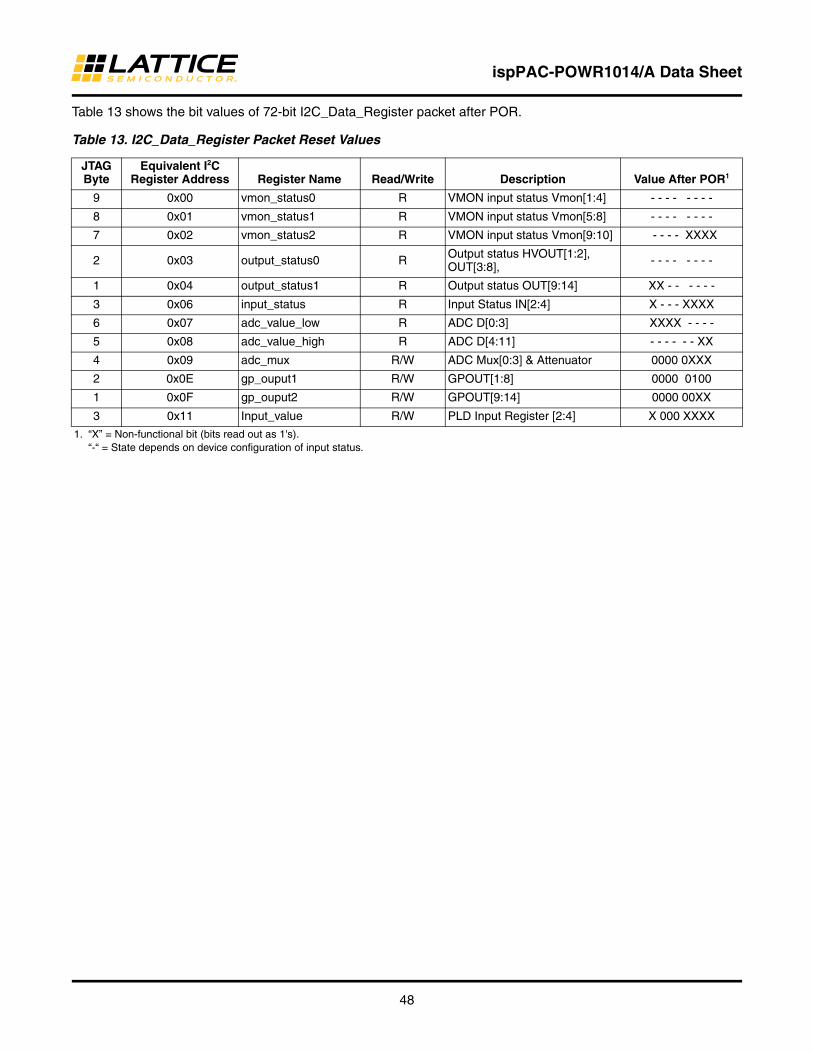
ispPAC-POWR1014/A Data Sheet
48
Table 13 shows the bit values of 72-bit I2C_Data_Register packet after POR.
Table 13. I2C_Data_Register Packet Reset Values
JTAG Byte
Equivalent I2C Register Address Register Name Read/Write Description Value After POR1
9 0x00 vmon_status0 R VMON input status Vmon[1:4] - - - - - - - -
8 0x01 vmon_status1 R VMON input status Vmon[5:8] - - - - - - - -
7 0x02 vmon_status2 R VMON input status Vmon[9:10] - - - - XXXX
2 0x03 output_status0 R Output status HVOUT[1:2], OUT[3:8], - - - - - - - -
1 0x04 output_status1 R Output status OUT[9:14] XX - - - - - -
3 0x06 input_status R Input Status IN[2:4] X - - - XXXX
6 0x07 adc_value_low R ADC D[0:3] XXXX - - - -
5 0x08 adc_value_high R ADC D[4:11] - - - - - - XX
4 0x09 adc_mux R/W ADC Mux[0:3] & Attenuator 0000 0XXX
2 0x0E gp_ouput1 R/W GPOUT[1:8] 0000 0100
1 0x0F gp_ouput2 R/W GPOUT[9:14] 0000 00XX
3 0x11 Input_value R/W PLD Input Register [2:4] X 000 XXXX
1. “X” = Non-functional bit (bits read out as 1's). “-“ = State depends on device configuration of input status.
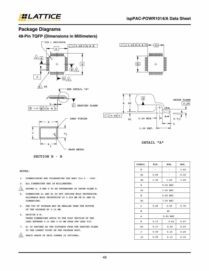
ispPAC-POWR1014/A Data Sheet
49
Package Diagrams48-Pin TQFP (Dimensions in Millimeters)
EXACT SHAPE OF EACH CORNER IS OPTIONAL.
TO THE LOWEST POINT ON THE PACKAGE BODY.
7. A1 IS DEFINED AS THE DISTANCE FROM THE SEATING PLANE
BASE METAL
LEAD BETWEEN 0.10 AND 0.25 MM FROM THE LEAD TIP.
1. DIMENSIONING AND TOLERANCING PER ANSI Y14.5 - 1982.
THESE DIMENSIONS APPLY TO THE FLAT SECTION OF THE
ALLOWABLE MOLD PROTRUSION IS 0.254 MM ON D1 AND E1
DATUMS A, B AND D TO BE DETERMINED AT DATUM PLANE H.
4. DIMENSIONS D1 AND E1 DO NOT INCLUDE MOLD PROTRUSION.
5. THE TOP OF PACKAGE MAY BE SMALLER THAN THE BOTTOM
8.
OF THE PACKAGE BY 0.15 MM.
DIMENSIONS.
2. ALL DIMENSIONS ARE IN MILLIMETERS.
6. SECTION B-B:
3.
1b
0.220.17b 0.27
0.16
0.23
0.200.09c
c1 0.09
b1 0.17
0.15
0.13
0.20
MAX.
1.60
0.15
0.75
1.45
e
N
L 0.45
0.50 BSC
0.60
48
E1
E
D1
D
9.00 BSC
7.00 BSC
9.00 BSC
7.00 BSC
A2
A1
1.35
0.05
SYMBOL
A -
MIN.
1.40
-
NOM.
-
C A-B D
SEE DETAIL "A"
LEAD FINISH
C SEATING PLANE
A3.
0.08
c
b
1c
M C
b
A -B D
3.D
4X8.
e
B 3.
E
D0.20
GAUGE PLANE
A1
0.08 C
A A2
1.00 REF.
L
0.20 MIN.B
0-7∞
B
H
E1
0.25
0.20 DA-BH D1
SECTION B - B
DETAIL "A"
NOTES:
PIN 1 INDICATOR
1
N

ispPAC-POWR1014/A Data Sheet
50
Part Number Description
Device Number
ispPAC-POWR1014X - 0XXX48X
Operating Temperature Range I = Industrial (-40oC to +85oC)
Package T = 48-pin TQFP TN = Lead-Free 48-pin TQFP*
Performance Grade 01 = 6V to 10V HVOUT 02 = 6V to 12V HVOUT
ADC Support A = ADC present
Device Family
ispPAC-POWR1014/A Ordering InformationConventional Packaging
Lead-Free Packaging
Part Number Package Pins
ispPAC-POWR1014A-01T48I TQFP 48
ispPAC-POWR1014-01T48I TQFP 48
ispPAC-POWR1014A-02T48I TQFP 48
ispPAC-POWR1014-02T48I TQFP 48
Part Number Package Pins
ispPAC-POWR1014A-01TN48I Lead-Free TQFP 48
ispPAC-POWR1014-01TN48I Lead-Free TQFP 48
ispPAC-POWR1014A-02TN48I Lead-Free TQFP 48
ispPAC-POWR1014-02TN48I Lead-Free TQFP 48

ispPAC-POWR1014/A Data Sheet
51
Package Options
ispPAC-POWR1014A48-Pin TQFP
123
456
789
101112
13 14 15 16 17 18 19 20 21 22 23 24
363534
333231
302928
272625
48 47 46 45 44 43 42 41 40 39 38 37
OUT14
OUT13
OUT12
OUT11
OUT10
OUT9
OUT8
OUT7
OUT6
OUT5
OUT4
GNDD
VMON9
VMON8
VMON7
VMON6
VMON5
GNDD
VCCA
VMON4
VMON3
VMON2
VMON1
GNDA
IN4
IN3
IN2
VC
CIN
P
IN1
MC
LK
VC
CD
RE
SE
TB
SC
L
SD
A
VM
ON
10
PLD
CLK
SM
BA
_OU
T3
HV
OU
T2
HV
OU
T1
TM
S
ATD
I
TD
I
VC
CJ
TD
O
TC
K
VC
CD
AP
S
TD
ISE
L
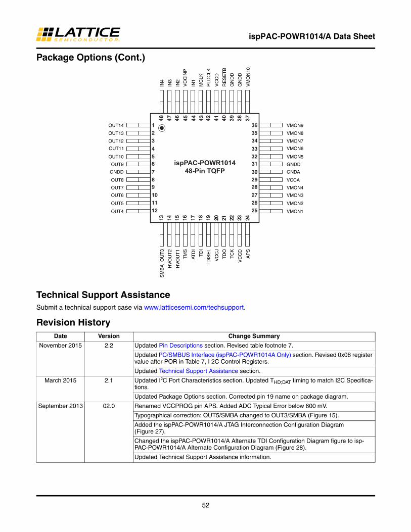
ispPAC-POWR1014/A Data Sheet
52
Package Options (Cont.)
Technical Support AssistanceSubmit a technical support case via www.latticesemi.com/techsupport.
Revision HistoryDate Version Change Summary
November 2015 2.2 Updated Pin Descriptions section. Revised table footnote 7.
Updated I2C/SMBUS Interface (ispPAC-POWR1014A Only) section. Revised 0x08 register value after POR in Table 7, I 2C Control Registers.
Updated Technical Support Assistance section.
March 2015 2.1 Updated I2C Port Characteristics section. Updated THD;DAT timing to match I2C Specifica-tions.
Updated Package Options section. Corrected pin 19 name on package diagram.
September 2013 02.0 Renamed VCCPROG pin APS. Added ADC Typical Error below 600 mV.
Typographical correction: OUT5/SMBA changed to OUT3/SMBA (Figure 15).
Added the ispPAC-POWR1014/A JTAG Interconnection Configuration Diagram (Figure 27).
Changed the ispPAC-POWR1014/A Alternate TDI Configuration Diagram figure to isp-PAC-POWR1014/A Alternate Configuration Diagram (Figure 28).
Updated Technical Support Assistance information.
ispPAC-POWR101448-Pin TQFP
123
456
789
101112
13 14 15 16 17 18 19 20 21 22 23 24
363534
333231
302928
272625
48 47 46 45 44 43 42 41 40 39 38 37
OUT14
OUT13
OUT12
OUT11
OUT10
OUT9
OUT8
OUT7
OUT6
OUT5
OUT4
GNDD
VMON9
VMON8
VMON7
VMON6
VMON5
GNDD
VCCA
VMON4
VMON3
VMON2
VMON1
GNDA
IN4
IN3
IN2
VC
CIN
P
IN1
MC
LK
VC
CD
RE
SE
TB
VM
ON
10
GN
DD
GN
DD
PLD
CLK
SM
BA
_OU
T3
HV
OU
T2
HV
OU
T1
TM
S
ATD
I
TD
I
VC
CJ
TD
O
TC
K
VC
CD
AP
S
TD
ISE
L
ispPAC-POWR1014/A Data Sheet
53
February 2011 01.9 Updated document with new corporate logo.
November 2009 01.8 Added ESD Performance table.
November 2009 01.7 VCCPROG pin usage further clarified.
Added Accessing I2C Registers Through JTAG section.
Added product information for the ispPAC-POWR1014-02 and ispPAC-POWR1014A-02.
June 2008 01.6 Added timing diagram and timing parameters to "Power-On Reset" specifications.
Modified PLD Architecture figure to show input registers.
Updated I2C Control Registers table.
VCCPROG pin usage clarification added.
August 2007 01.5 Changes to HVOUT pin specifications.
March 2007 01.4 Corrected VCCINP Voltage range from "2.25 V to 3.6 V" to "2.25 V to 5.5 V".
Removed reference to Internal Pull-up resistor for signal line TDO.
Corrected the Maximum Vmon Range value from 5.734V to 5.867V.
Removed references to VPS[0:1].
October 2006 01.3 Data sheet status changed to “Final”
Analog Specifications table, reduced Max. ICC to 20 mA.
Tightened Input Resistor Variation to 15%.
AC/Transient Characteristics table, tightened Internal Oscillator frequency variation down to 5%.
Digital Specifications table, included VIL and VIH specifications for I2C interface.
May 2006 01.2 Update HVOUT I source range: 12.5µA to 100µA
Clarify operation of ADC conversions
Digital Specifications table, added footnotes on I2C frequency
TAP Instructions table, clarify DISCHARGE instruction of JTAG. Added instruction descrip-tions for others.
March 2006 01.1 ispPAC-POWR1014/A block diagram: “SELTDI” changed to “TDISEL”.
Pin Descriptions table: “InxP” changed to “Inx”, “MONx” to “VMONx”, VMON upper range from “5.75 V” to “5.87 V”.
Pin Descriptions table, note 4 - clarification for un-used VMON pins to be tied to GNDD.
Absolute Maximum Ratings table and Recommended Operating Conditions table: “VMON+” changed to VMON”.
Digital Specifications table: add note # 2 to ISINKTOTAL: “Sum of maximum current sink by all digital outputs. Reliable operation is not guaranteed if this value is exceeded.”
Typographical corrections: Vmon trip points and thresholds
Typographical corrections: “InxP” to “Inx”, “MONx” to “VMONx”.
February 2006 01.0 Initial release.
Date Version Change Summary