ds100br210 ultra low power 10.3 gbps 2-channel repeater
TRANSCRIPT
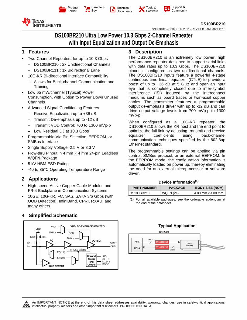
IN+
IN-
EQ
IDLE DETECT
OUTBUFSMBus
VOD/ DE-EMPHASIS CONTROLVDD
SMBus
Tx IDLE Enable
DEM
EQ[1:0]
OUT+
OUT-
50:50:
VOD
SMBus
LOSChannelStatus
andControl
SD_THTX_DISMODE
Line Card
2x10G
ASIC
FPGA2x10G
2 x SFP+
(Stacked)
DS100BR210
DS100BR210
Product
Folder
Sample &Buy
Technical
Documents
Tools &
Software
Support &Community
DS100BR210SNLS348E –OCTOBER 2011–REVISED JANUARY 2015
DS100BR210 Ultra Low Power 10.3 Gbps 2-Channel Repeaterwith Input Equalization and Output De-Emphasis
1 Features 3 DescriptionThe DS100BR210 is an extremely low power, high
1• Two Channel Repeaters for up to 10.3 Gbpsperformance repeater designed to support serial links– DS100BR210 : 2x Unidirectional Channels with data rates up to 10.3 Gbps. The DS100BR210
– DS100BR111 : 1x Bidirectional Lane pinout is configured as two unidirectional channels.The DS100BR210 inputs feature a powerful 4-stage• 10G-KR Bi-directional Interface Compatibilitycontinuous time linear equalizer (CTLE) to provide a– Allows for Back-channel Communication and boost of up to +36 dB at 5 GHz and open an inputTraining eye that is completely closed due to inter-symbol
• Low 65 mW/channel (Typical) Power interference (ISI) induced by the interconnectConsumption, with Option to Power Down Unused mediums such as board traces or twin-axial copper
cables. The transmitter features a programmableChannelsoutput de-emphasis driver with up to -12 dB and can• Advanced Signal Conditioning Featuresdrive output voltage levels from 700 mVp-p to 1300
– Receive Equalization up to +36 dB mVp-p.– Transmit De-emphasis up to -12 dB When configured as a 10G-KR repeater, the– Transmit VOD Control: 700 to 1300 mVp-p DS100BR210 allows the KR host and the end point to
optimize the full link by adjusting transmit and receive– Low Residual DJ at 10.3 Gbpsequalizer coefficients using back-channel• Programmable Via Pin Selection, EEPROM, orcommunication techniques specified by the 802.3apSMBus Interface Ethernet standard.
• Single Supply Voltage: 2.5 V or 3.3 VThe programmable settings can be applied via pin• Flow-thru Pinout in 4 mm × 4 mm 24-pin Leadless control, SMBus protocol, or an external EEPROM. InWQFN Package the EEPROM mode, the configuration information is
• 5 kV HBM ESD Rating automatically loaded on power up, thereby eliminatingthe need for an external microprocessor or software• -40 to 85°C Operating Temperature Rangedriver.
2 ApplicationsDevice Information(1)
• High-speed Active Copper Cable Modules and PART NUMBER PACKAGE BODY SIZE (NOM)FR-4 Backplane in Communication Systems
DS100BR210 WQFN (24) 4.00 mm x 4.00 mm• 10GE, 10G-KR, FC, SAS, SATA 3/6 Gbps (with
(1) For all available packages, see the orderable addendum atOOB Detection), InfiniBand, CPRI, RXAUI and the end of the datasheet.many others
4 Simplified Schematic
Typical Application
1
An IMPORTANT NOTICE at the end of this data sheet addresses availability, warranty, changes, use in safety-critical applications,intellectual property matters and other important disclaimers. PRODUCTION DATA.

DS100BR210SNLS348E –OCTOBER 2011–REVISED JANUARY 2015 www.ti.com
Table of Contents8.3 Feature Description................................................. 131 Features .................................................................. 18.4 Device Functional Modes........................................ 132 Applications ........................................................... 18.5 Programming........................................................... 153 Description ............................................................. 18.6 Register Maps ......................................................... 294 Simplified Schematic............................................. 1
9 Application and Implementation ........................ 365 Revision History..................................................... 29.1 Application Information............................................ 366 Pin Configuration and Functions ......................... 39.2 Typical Application ................................................. 377 Specifications......................................................... 6 10 Power Supply Recommendations ..................... 447.1 Absolute Maximum Ratings ...................................... 610.1 3.3-V or 2.5-V Supply Mode Operation................. 447.2 ESD Ratings ............................................................ 610.2 Power Supply Bypass ........................................... 457.3 Recommended Operating Conditions....................... 6
11 Layout................................................................... 457.4 Thermal Information .................................................. 611.1 Layout Guidelines ................................................. 457.5 Electrical Characteristics........................................... 711.2 Layout Example .................................................... 457.6 Electrical Characteristics — Serial Management Bus
12 Device and Documentation Support ................. 47Interface .................................................................... 912.1 Documentation Support ........................................ 477.7 Timing Requirements — LOS and ENABLE /
DISABLE Timing ........................................................ 9 12.2 Trademarks ........................................................... 477.8 Typical Characteristics ............................................ 11 12.3 Electrostatic Discharge Caution............................ 47
8 Detailed Description ............................................ 12 12.4 Glossary ................................................................ 478.1 Overview ................................................................. 12 13 Mechanical, Packaging, and Orderable8.2 Functional Block Diagram ....................................... 12 Information ........................................................... 47
5 Revision HistoryNOTE: Page numbers for previous revisions may differ from page numbers in the current version.
Changes from Revision D (April 2013) to Revision E Page
• Added, updated, or renamed the following sections: Device Information Table, Application and Implementation;Power Supply Recommendations; Layout; Device and Documentation Support; Mechanical, Packaging, andOrdering Information .............................................................................................................................................................. 1
• Added Thermal Information ................................................................................................................................................... 6
2 Submit Documentation Feedback Copyright © 2011–2015, Texas Instruments Incorporated
Product Folder Links: DS100BR210

OUTA+
OUTA-
OUTB+
VD
D_S
EL
VIN
18
INB+
INB-
171413 16
LOS
____
___
VO
D_S
EL
/ RE
AD
EN
____
_M
OD
E /
DO
NE
SD
_TH
INA+
INA-
OUTB-
SMBUS AND CONTROL
15
VDD
24
23
22
21
20
19
11
12
8
10
9
7
EQ
B1/
AD
2
EN
SM
B
1256 3
SC
L/D
EM
B
EQ
B0/
AD
3
SD
A/D
EM
A4
VDD
TX
_DIS
AD1/EQA1
AD0/EQA0
DS100BR210www.ti.com SNLS348E –OCTOBER 2011–REVISED JANUARY 2015
6 Pin Configuration and Functions
RTW Package24 Pins WQFN
Top View
(1) The center DAP on the package bottom is the device GND connection. This pad must be connected to GND throughmultiple (minimum of 4) vias to ensure optimal electrical and thermal performance.
Pin Functions (1)
PINI/O, TYPE DESCRIPTION
NAME NUMBERDIFFERENTIAL HIGH SPEED I/O's
Inverting and non-inverting CML differential inputs to the equalizer. On-chip 50 ΩINA+, INA- , 7, 8 I, CML termination resistors connect both INx+ and INx- to VDD. Compatible with AC coupledINB+, INB- 11, 12 CML inputs.OUTA+, OUTA-, 24, 23 Inverting and non-inverting 50 Ω driver outputs with de-emphasis. Compatible with ACO, CMLOUTB+, OUTB- 20, 19 coupled CML inputs.CONTROL PINS
System Management Bus (SMBus) Enable PinI, 4-LEVEL, High = Register Access SMBus Slave ModeENSMB 3 LVCMOS Float = Read External EEPROM (SMBus Master Mode)
Tie 1 kΩ to GND = Pin Mode
(1) LVCMOS inputs without the “Float” conditions must be driven to a logic low or high at all times or operation is not guaranteed. Unlessthe "Float" level is desired, 4-Level input pins require a minimum 1 kΩ resistor to GND, VDD (in 2.5 V mode), or VIN (in 3.3 V mode).Input edge rate for LVCMOS/FLOAT inputs must be faster than 50 ns from 10–90%.
Copyright © 2011–2015, Texas Instruments Incorporated Submit Documentation Feedback 3
Product Folder Links: DS100BR210
DS100BR210SNLS348E –OCTOBER 2011–REVISED JANUARY 2015 www.ti.com
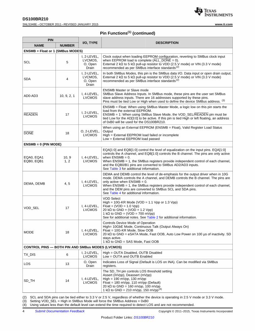
Pin Functions(1) (continued)PIN
I/O, TYPE DESCRIPTIONNAME NUMBER
ENSMB = Float or 1 (SMBus MODES)I, 2-LEVEL, Clock output when loading EEPROM configuration, reverting to SMBus clock inputLVCMOS, when EEPROM load is complete (ALL_DONE = 0).SCL 5 O, Open External 2 kΩ to 5 kΩ pull-up resistor to VDD (2.5 V mode) or VIN (3.3 V mode)
Drain recommended as per SMBus interface standards (2)
I, 2-LEVEL, In both SMBus Modes, this pin is the SMBus data I/O. Data input or open drain output.LVCMOS, External 2 kΩ to 5 kΩ pull-up resistor to VDD (2.5 V mode) or VIN (3.3 V mode)SDA 4 O, Open recommended as per SMBus interface standards (2)
DrainENSMB Master or Slave mode
I, 4-LEVEL, SMBus Slave Address Inputs. In SMBus mode, these pins are the user set SMBusAD0-AD3 10, 9, 2, 1 LVCMOS slave address inputs. There are 16 addresses supported by these pins.Pins must be tied Low or High when used to define the device SMBus address. (3)
ENSMB = Float: When using SMBus Master Mode, a logic low on this pin starts theload from the external EEPROM.I, 2-LEVEL,READEN 17 ENSMB = 1: When using SMBus Slave Mode, the VOD_SEL/READEN pin must beLVCMOS tied Low for the AD[3:0] to be active. If this pin is tied High or left floating, an addressof 0xB0 will be used for the DS100BR210.When using an External EEPROM (ENSMB = Float), Valid Register Load Status
O, 2-LEVEL, OutputDONE 18 LVCMOS High = External EEPROM load failed or incompleteLow = External EEPROM load passed
ENSMB = 0 (PIN MODE)EQA[1:0] and EQB[1:0] control the level of equalization on the input pins. EQA[1:0]controls the A channel, and EQB[1:0] controls the B channel. The pins are only active
EQA0, EQA1 10, 9 I, 4-LEVEL, when ENSMB = 0.EQB0, EQB1 1, 2 LVCMOS When ENSMB = 1, the SMBus registers provide independent control of each channel,
and the EQB0/B1 pins are converted to SMBus AD2/AD3 inputs.See Table 3 for additional information.DEMA and DEMB control the level of de-emphasis for the output driver when in 10Gmode. DEMA controls the A channel, and DEMB controls the B channel. The pins are
I, 4-LEVEL, only active when ENSMB = 0.DEMA, DEMB 4, 5 LVCMOS When ENSMB = 1, the SMBus registers provide independent control of each channel,and the DEM pins are converted to SMBus SCL and SDA pins.See Table 4 for additional information.VOD SelectHigh = 10G-KR Mode (VOD = 1.1 Vpp or 1.3 Vpp)
I, 4-LEVEL, Float = (VOD = 1.0 Vpp)VOD_SEL 17 LVCMOS 20 kΩ to GND = (VOD = 1.2 Vpp)1 kΩ to GND = (VOD = 700 mVpp)See for additional notes. See Table 2 for additional information.Controls Device Mode of OperationHigh= 10GbE Mode, Continuous Talk (Output Always On)
I, 4-LEVEL, Float = 10G-KR Mode, Slow OOBMODE 18 LVCMOS 20 kΩ to GND = eSATA Mode, Fast OOB, Auto Low Power on 100 µs of inactivity. SDstays active.1 kΩ to GND = SAS Mode, Fast OOB
CONTROL PINS — BOTH PIN AND SMBus MODES (LVCMOS)I, 2-LEVEL, High = OUTA Disabled, OUTB DisabledTX_DIS 6 LVCMOS Low = OUTA and OUTB Enabled
O, Open Indicates Loss of Signal (Default is LOS on INA). Can be modified via SMBusLOS 13 Drain registers.The SD_TH pin controls LOS threshold settingAssert (mVpp), Deassert (mVpp)
I, 4-LEVEL, High = 190 mVpp, 130 mVppSD_TH 14 LVCMOS Float = 180 mVpp, 110 mVpp (Default)20 kΩ to GND = 160 mVpp, 100 mVpp1 kΩ to GND = 210 mVpp, 150 mVpp (4)
(2) SCL and SDA pins can be tied either to 3.3 V or 2.5 V, regardless of whether the device is operating in 2.5 V mode or 3.3 V mode.(3) Setting VOD_SEL = High in SMBus Mode will force the SMBus Address = 0xB0(4) Using values less than the default level can extend the time required to detect LOS and are not recommended.
4 Submit Documentation Feedback Copyright © 2011–2015, Texas Instruments Incorporated
Product Folder Links: DS100BR210
DS100BR210www.ti.com SNLS348E –OCTOBER 2011–REVISED JANUARY 2015
Pin Functions(1) (continued)PIN
I/O, TYPE DESCRIPTIONNAME NUMBER
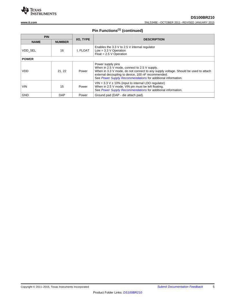
Enables the 3.3 V to 2.5 V internal regulatorVDD_SEL 16 I, FLOAT Low = 3.3 V Operation
Float = 2.5 V OperationPOWER
Power supply pinsWhen in 2.5 V mode, connect to 2.5 V supply.
VDD 21, 22 Power When in 3.3 V mode, do not connect to any supply voltage. Should be used to attachexternal decoupling to device, 100 nF recommended.See Power Supply Recommendations for additional information.VIN = 3.3 V ± 10% (input to internal LDO regulator)
VIN 15 Power When in 2.5 V mode, VIN pin must be left floating.See Power Supply Recommendations for additional information.
GND DAP Power Ground pad (DAP - die attach pad).
Copyright © 2011–2015, Texas Instruments Incorporated Submit Documentation Feedback 5
Product Folder Links: DS100BR210

DS100BR210SNLS348E –OCTOBER 2011–REVISED JANUARY 2015 www.ti.com
7 Specifications
7.1 Absolute Maximum Ratings (1) (2)
MIN MAX UNITSupply Voltage (VDD) -0.5 2.75 VSupply Voltage (VIN) -0.5 4.0 VLVCMOS Input/Output Voltage -0.5 4.0 VCML Input Voltage -0.5 (VDD+0.5) VCML Input Current -30 30 mAJunction Temperature 125 °CStorage Temperature Range Tstg -40 125 °C
(1) “Absolute Maximum Ratings” indicate limits beyond which damage to the device may occur, including inoperability and degradation ofdevice reliability and/or performance. Functional operation of the device and/or non-degradation at the Absolute Maximum Ratings orother conditions beyond those indicated in the Recommended Operating Conditions is not implied.
(2) For soldering specifications, see SNOA549.
7.2 ESD RatingsVALUE UNIT
Human-body model (HBM), per ANSI/ESDA/JEDEC JS-001 (1) ±5000V(ESD) Electrostatic discharge VCharged-device model (CDM), per JEDEC specification JESD22- ±1250C101 (2)
(1) JEDEC document JEP155 states that 500-V HBM allows safe manufacturing with a standard ESD control process.(2) JEDEC document JEP157 states that 250-V CDM allows safe manufacturing with a standard ESD control process.
7.3 Recommended Operating Conditions (1)
MIN NOM MAX UNITSupply Voltage (2.5 V mode) 2.375 2.5 2.625 VSupply Voltage (3.3 V mode) 3.0 3.3 3.6 VAmbient Temperature -40 25 +85 °CSMBus (SDA, SCL) 3.6 V
(1) The Recommended Operating Conditions indicate conditions at which the device is functional and the device should not be operatedbeyond such conditions. Absolute Maximum Numbers are guaranteed for a junction temperature range of -40°C to +125°C. Models arevalidated to Maximum Operating Voltages only.
7.4 Thermal InformationRTW
THERMAL METRIC (1) WQFN UNIT(24 PINS)
RθJA Junction-to-ambient thermal resistance, No Airflow, 4 layer JEDEC 33.0°C/W
RθJC(top) Junction-to-case (top) thermal resistance 3.2
(1) For more information about traditional and new thermal metrics, see the IC Package Thermal Metrics application report, SPRA953.
6 Submit Documentation Feedback Copyright © 2011–2015, Texas Instruments Incorporated
Product Folder Links: DS100BR210

DS100BR210www.ti.com SNLS348E –OCTOBER 2011–REVISED JANUARY 2015
7.5 Electrical CharacteristicsPARAMETER TEST CONDITIONS MIN TYP MAX UNIT
POWER SUPPLY CURRENTTX_DIS = Low, EQ = ON 50 63VOD_SEL = Float (1000 mVpp)Auto Low Power Mode
IDD Supply Current TX_DIS = Low, MODE = 20 kΩ mA12 15VID CHA and CHB = 0.0 VVOD_SEL = Float (1000 mVpp)TX_DIS = High 25 35
LVCMOS DC SPECIFICATIONSHigh Level Input Voltage,VIH25 2.5 V Supply Mode 2.0 VDD V2-Level LVCMOSHigh Level Input Voltage,VIH33 3.3 V Supply Mode 2.0 VIN V2-Level LVCMOSLow Level Input Voltage,VIL GND 0.7 V2-Level LVCMOS
VOH High Level Output Voltage IOH = -4.0 mA (1) 2.0 VVOL Low Level Output Voltage IOL = 4.0 mA 0.4 V
Vinput = 0 V or VDD -15 +15VDD_SEL = FloatIIN Input Leakage Current µA
Vinput = 0 V or VIN -15 +15VDD_SEL = LowVinput = 0 V or VDD - 0.05 V
Input Leakage Current VDD_SEL = FloatIIN-P -160 +80 µA4-Level Input (2) Vinput = 0 V or VIN - 0.05 VVDD_SEL = Low
CML RECEIVER INPUTSSource Transmit Launch Default power-up conditionsVTX 190 800 1600 mVp-pDifferential Signal Level ENSMB = 0 or 1
SDD11 @ 4.1 GHz -12RLRX-IN RX return loss SDD11 @ 11.1 GHz -8 dB
SCD11 @ 11.1 GHz -10HIGH SPEED TRANSMITTER OUTPUTS
OUT+ and OUT- AC coupled andterminated by 50 Ω to GNDVOD1 Output Voltage Differential Swing 500 650 800VOD_SEL = Low (700 mVpp setting)DE = LowOUT+ and OUT- AC coupled andterminated by 50 Ω to GNDVOD2 Output Voltage Differential Swing 800 1000 1100VOD_SEL = Float (1000 mVpp setting) mVp-pDE = LowOUT+ and OUT- AC coupled andterminated by 50 Ω to GND
VOD3 Output Voltage Differential Swing VOD_SEL = 20 kΩ to GND (1200 950 1150 1350mVpp)DE = LowOUT+ and OUT- AC coupled andterminated by 50 Ω to GNDVOD_DE1 De-Emphasis Levels -3.5 dBVOD_SEL = Float (1000 mVpp)DE = FloatOUT+ and OUT- AC coupled andterminated by 50 Ω to GNDVOD_DE2 De-Emphasis Levels -6 dBVOD_SEL = Float (1000 mVpp)DE = 20 kΩ to GND
(1) VOH only applies to the DONE pin; LOS, SCL, and SDA are open-drain outputs that have no internal pull-up capability. DONE is a fullLVCMOS output with pull-up and pull-down capability.
(2) Input is held to a maximum of 50 mV below VDD or VIN to simulate the use of a 1 kΩ resistor on the input.
Copyright © 2011–2015, Texas Instruments Incorporated Submit Documentation Feedback 7
Product Folder Links: DS100BR210
DS100BR210SNLS348E –OCTOBER 2011–REVISED JANUARY 2015 www.ti.com
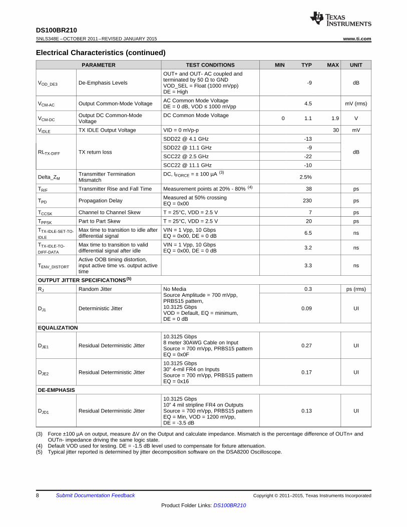
Electrical Characteristics (continued)PARAMETER TEST CONDITIONS MIN TYP MAX UNIT
OUT+ and OUT- AC coupled andterminated by 50 Ω to GNDVOD_DE3 De-Emphasis Levels -9 dBVOD_SEL = Float (1000 mVpp)DE = HighAC Common Mode VoltageVCM-AC Output Common-Mode Voltage 4.5 mV (rms)DE = 0 dB, VOD ≤ 1000 mVpp
Output DC Common-Mode DC Common Mode VoltageVCM-DC 0 1.1 1.9 VVoltageVIDLE TX IDLE Output Voltage VID = 0 mVp-p 30 mV
SDD22 @ 4.1 GHz -13SDD22 @ 11.1 GHz -9
RLTX-DIFF TX return loss dBSCC22 @ 2.5 GHz -22SCC22 @ 11.1 GHz -10
Transmitter Termination DC, IFORCE = ± 100 µA (3)Delta_ZM 2.5%MismatchTR/F Transmitter Rise and Fall Time Measurement points at 20% - 80% (4) 38 ps
Measured at 50% crossingTPD Propagation Delay 230 psEQ = 0x00TCCSK Channel to Channel Skew T = 25°C, VDD = 2.5 V 7 psTPPSK Part to Part Skew T = 25°C, VDD = 2.5 V 20 psTTX-IDLE-SET-TO- Max time to transition to idle after VIN = 1 Vpp, 10 Gbps 6.5 nsIDLE differential signal EQ = 0x00, DE = 0 dBTTX-IDLE-TO- Max time to transition to valid VIN = 1 Vpp, 10 Gbps 3.2 nsDIFF-DATA differential signal after idle EQ = 0x00, DE = 0 dB
Active OOB timing distortion,TENV_DISTORT input active time vs. output active 3.3 ns
timeOUTPUT JITTER SPECIFICATIONS (5)
RJ Random Jitter No Media 0.3 ps (rms)Source Amplitude = 700 mVpp,PRBS15 pattern,10.3125 GbpsDJ1 Deterministic Jitter 0.09 UIVOD = Default, EQ = minimum,DE = 0 dB
EQUALIZATION10.3125 Gbps8 meter 30AWG Cable on InputDJE1 Residual Deterministic Jitter 0.27 UISource = 700 mVpp, PRBS15 patternEQ = 0x0F10.3125 Gbps30" 4-mil FR4 on InputsDJE2 Residual Deterministic Jitter 0.17 UISource = 700 mVpp, PRBS15 patternEQ = 0x16
DE-EMPHASIS10.3125 Gbps10” 4 mil stripline FR4 on Outputs
DJD1 Residual Deterministic Jitter Source = 700 mVpp, PRBS15 pattern 0.13 UIEQ = Min, VOD = 1200 mVpp,DE = -3.5 dB
(3) Force ±100 µA on output, measure ΔV on the Output and calculate impedance. Mismatch is the percentage difference of OUTn+ andOUTn- impedance driving the same logic state.
(4) Default VOD used for testing. DE = -1.5 dB level used to compensate for fixture attenuation.(5) Typical jitter reported is determined by jitter decomposition software on the DSA8200 Oscilloscope.
8 Submit Documentation Feedback Copyright © 2011–2015, Texas Instruments Incorporated
Product Folder Links: DS100BR210

DS100BR210www.ti.com SNLS348E –OCTOBER 2011–REVISED JANUARY 2015
7.6 Electrical Characteristics — Serial Management Bus InterfaceOver recommended operating supply and temperature ranges unless other specified.
PARAMETER TEST CONDITIONS MIN TYP MAX UNITSERIAL BUS INTERFACE DC SPECIFICATIONS (1)
VIL Data, Clock Input Low Voltage 0.8 VVIH Data, Clock Input High Voltage 2.1 3.6 VIPULLUP Current Through Pull-Up Resistor High Power Specification 4 mAor Current SourceVDD Nominal Bus Voltage 2.375 3.6 VILEAK-Bus Input Leakage Per Bus Segment See (2) -200 +200 µACI Capacitance for SDA and SCL See (2) (3) (4) 10 pFRTERM External Termination Resistance Pullup VDD = 3.3 V, See (2) (3) (5) 2000 Ω
pull to VDD = 2.5V ± 5% OR 3.3V ± Pullup VDD = 2.5 V, See (2) (3) (5)1000 Ω10%
SERIAL BUS INTERFACE TIMING SPECIFICATIONSENSMB = VDD (Slave Mode) 400 kHz
FSMB Bus Operating FrequencyENSMB = Float (Master Mode) (1) 280 400 520 kHz
Bus Free Time Between Stop andTBUF 1.3 µsStart ConditionTHD:STA Hold time after (Repeated) Start At IPULLUP, Max
Condition. After this period, the 0.6 µsfirst clock is generated.
TSU:STA Repeated Start Condition Setup 0.6 µsTimeTSU:STO Stop Condition Setup Time 0.6 µsTHD:DAT Data Hold Time 0 nsTSU:DAT Data Setup Time 100 nsTLOW Clock Low Period 1.3 µsTHIGH Clock High Period See (6) 0.6 50 µstF Clock/Data Fall Time See (6) 300 nstR Clock/Data Rise Time See (6) 300 ns
Time in which a device must betPOR See (4) (6) 500 msoperational after power-on reset
(1) EEPROM interface requires 1 MHz capable EEPROM device.(2) Recommended value.(3) Recommended maximum capacitance load per bus segment is 400 pF.(4) Guaranteed by design and characterization. Parameter not tested in production.(5) Maximum termination voltage should be identical to the device supply voltage.(6) Compliant to SMBus 2.0 physical layer specification. See System Management Bus (SMBus) Specification Version 2.0, section 3.1.1
SMBus common AC specifications for details.
7.7 Timing Requirements — LOS and ENABLE / DISABLE TimingMIN NOM MAX UNIT
Input IDLE to ActiveTLOS_OFF See (1) 0.035 µsRX_LOS response timeInput Active to IDLETLOS_ON See (1) 0.4 µsRX_LOS response timeTX Disable assert TimeTOFF See (1) 0.005 µsTX_DIS = High to Output OFFTX Disable negateTimeTON See (1) 0.150 µsTX_DIS = Low to Output ONAuto Low Power ExitTLP_EXIT See (1) 150 nsALP to Normal OperationAuto Low Power EnterTLP_ENTER See (1) 100 µsNormal Operation to Auto Low Power
(1) Parameter not tested in production.
Copyright © 2011–2015, Texas Instruments Incorporated Submit Documentation Feedback 9
Product Folder Links: DS100BR210

SP
tBUFtHD:STA
tLOW
tR
tHD:DAT
tHIGH
tFtSU:DAT
tSU:STA
ST SP
tSU:STO
SCL
SDAST
IN
OUT
+
-tIDLE-DATA
+
-
tDATA-IDLE
DATA
IDLE
0V
0V
DATA
IDLE
IN 0V
tPLHD
OUT 0V
tPHLD
0V
20%
80%
20%
80%
tFALLtRISE
VOD = [Out+ - Out-]
DS100BR210SNLS348E –OCTOBER 2011–REVISED JANUARY 2015 www.ti.com
Figure 1. Output Rise and Fall Transition Times
Figure 2. Propagation Delay Timing Diagram
Figure 3. Transmit Idle-Data and Data-Idle Response Time
Figure 4. SMBus Timing Parameters
10 Submit Documentation Feedback Copyright © 2011–2015, Texas Instruments Incorporated
Product Folder Links: DS100BR210

0 1 2 3 4 5 6 7
500
600
700
800
900
1000
1100
1200
1300
1400
1500
Out
put V
olta
ge (
mV
pp)
VOD Level
700 800 900 1000 1100 1200 1300
0
10
20
30
40
50
60
70
80
90
100
Sup
ply
Cur
rent
(m
A)
Output Voltage (mVpp)
3.3V Mode
2.5V Mode
2.0 2.2 2.4 2.6 2.8 3.0
40
44
48
52
56
60
Sup
ply
Cur
rent
(m
A)
Supply Voltage (V)
2.5V Mode
DS100BR210www.ti.com SNLS348E –OCTOBER 2011–REVISED JANUARY 2015
7.8 Typical CharacteristicsThe following data was collected at 25°C.
VOD = 700 mVpp
Figure 5. Supply Current vs. Output Voltage Setting Figure 6. Supply Current vs. Supply Voltage
Figure 7. Output Voltage vs. Output Voltage Setting
Copyright © 2011–2015, Texas Instruments Incorporated Submit Documentation Feedback 11
Product Folder Links: DS100BR210
INA+
INA-EQ
OUTA+
OUTA-
A Channel
Term
Pre-driver Driver
EQA[1:0]
ENSMB
DEMA
Digital Core and SMBus RegistersSCL
SDA
TX_DIS
VIN
VDD_SEL
AD[3:0]
Internal voltage regulator
READEN DONE
VOD_SEL
INB+
INB-EQ
OUTB+
OUTB-
Term
EQB[1:0]
ENSMB
DEMB
VOD_SEL
B Channel
Signal Detect
Signal Detect
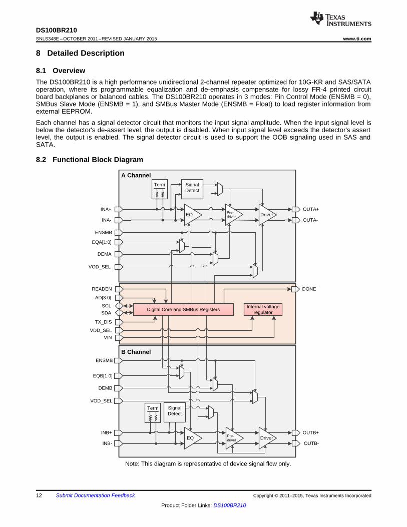
Note: This diagram is representative of device signal flow only.
DriverPre-driver
DS100BR210SNLS348E –OCTOBER 2011–REVISED JANUARY 2015 www.ti.com
8 Detailed Description
8.1 OverviewThe DS100BR210 is a high performance unidirectional 2-channel repeater optimized for 10G-KR and SAS/SATAoperation, where its programmable equalization and de-emphasis compensate for lossy FR-4 printed circuitboard backplanes or balanced cables. The DS100BR210 operates in 3 modes: Pin Control Mode (ENSMB = 0),SMBus Slave Mode (ENSMB = 1), and SMBus Master Mode (ENSMB = Float) to load register information fromexternal EEPROM.
Each channel has a signal detector circuit that monitors the input signal amplitude. When the input signal level isbelow the detector's de-assert level, the output is disabled. When input signal level exceeds the detector's assertlevel, the output is enabled. The signal detector circuit is used to support the OOB signaling used in SAS andSATA.
8.2 Functional Block Diagram
12 Submit Documentation Feedback Copyright © 2011–2015, Texas Instruments Incorporated
Product Folder Links: DS100BR210

DS100BR210www.ti.com SNLS348E –OCTOBER 2011–REVISED JANUARY 2015
8.3 Feature Description
8.3.1 4-Level Input Configuration GuidelinesThe 4-level input pins use a resistor divider to set the four valid control levels and provide a wider range ofcontrol settings when ENSMB = 0. There is an internal 30 kΩ pull-up and a 60 kΩ pull-down connected to thepackage pin. These resistors, together with the external resistor connection, combine to achieve the desiredvoltage level. By using the 1 kΩ pull-down, 20 kΩ pull-down, no connect, or 1 kΩ pull-up, the optimal voltagelevels for each of the four input states are achieved as shown in Table 1.
Table 1. 4–Level Control Pin SettingsRESULTING PIN VOLTAGE
LEVEL SETTING 3.3 V MODE 2.5 V MODE0 Tie 1 kΩ to GND 0.10 V 0.08 VR Tie 20 kΩ to GND 1/3 x VIN 1/3 x VDD
F Float (leave pin open) 2/3 x VIN 2/3 x VDD
1 Tie 1 kΩ to VIN or VDD VIN - 0.05 V VDD - 0.04 V
8.3.2 Typical 4-Level Input Thresholds• Internal Threshold between 0 and R = 0.2 * VIN or VDD• Internal Threshold between R and F = 0.5 * VIN or VDD• Internal Threshold between F and 1 = 0.8 * VIN or VDD
In order to minimize the startup current associated with the integrated 2.5 V regulator, the 1 kΩ pull-up / pull-down resistors are recommended. If several four level inputs require the same setting, it is possible to combinetwo or more 1 kΩ resistors into a single lower value resistor. As an example, combining two inputs with a single500 Ω resistor is a valid way to save board space.
8.4 Device Functional Modes
8.4.1 Pin Control ModeWhen in Pin Mode (ENSMB = 0), equalization, de-emphasis, and VOD (output amplitude) can be selected viaexternal pin control for both the A-channel and B-channel. Equalization and de-emphasis can be programmed bypin selection for each side independently. For further device control, the VOD_SEL and MODE pins are availableto improve DS100BR210 performance depending on design applications. The receiver electrical idle detectthreshold is also adjustable via the SD_TH pin. Pin control mode is ideal in situations where neither MCU orEEPROM is available to access the device via SMBus SDA and SCL lines.
8.4.2 SMBus Slave ModeWhen in Slave SMBus Mode (ENSMB = 1), equalization, de-emphasis, and VOD (output amplitude) are allprogrammable on an individual channel basis. Upon assertion of ENSMB, the EQx, DEMx, and VODx settingsare controlled by SMBus immediately. It is important to note that SMBus settings can only be changed from theirdefaults after asserting Register Enable by setting Reg 0x06[3] = 1. The EQx, DEMx, and VODx pins aresubsequently converted to AD0-AD3 SMBus address inputs. The other external control pins (TX_DIS, MODE,and SD_TH) remain active unless their respective registers are written to and the appropriate override bit is set.If the user overrides a pin control, the input voltage level of that control pin is ignored until ENSMB is driven low(Pin Mode). In the event that channels are powered down via the TX_DIS pin, register setting states are notaffected.
Table 2. Signal Detect Threshold Level (1)
SMBus REG bit TYPICAL ASSERT LEVEL TYPICAL DE-ASSERT LEVELLevel SD_TH (Pin 14) [3:2] and [1:0] (mVpp) (mVpp)1 0 10 210 1502 R 01 160 1003 F (Default) 00 180 110
(1) Typical assert and de-assert levels were measured with VDD = 2.5 V, 25°C, and 010101 pattern at 8 Gbps.
Copyright © 2011–2015, Texas Instruments Incorporated Submit Documentation Feedback 13
Product Folder Links: DS100BR210

DS100BR210SNLS348E –OCTOBER 2011–REVISED JANUARY 2015 www.ti.com
Device Functional Modes (continued)Table 2. Signal Detect Threshold Level(1) (continued)
SMBus REG bit TYPICAL ASSERT LEVEL TYPICAL DE-ASSERT LEVELLevel SD_TH (Pin 14) [3:2] and [1:0] (mVpp) (mVpp)4 1 11 190 130
8.4.3 SMBus Master ModeWhen in SMBus Master Mode (ENSMB = Float), the equalization, de-emphasis, and VOD (output amplitude) formultiple devices can be loaded via external EEPROM. By asserting a Float condition on the ENSMB pin, anexternal EEPROM writes register settings to each device in accordance with its SMBus slave address. Thesettings programmable by external EEPROM provide only a subset of all the register bits available via SMBusSlave Mode, and the bit-mapping between SMBus Slave Mode registers and EEPROM addresses can bereferenced in Table 6. Once the EEPROM successfully finishes loading each device's register settings, thedevice reverts back to SMBus Slave Mode and releases SDA and SCL control to an external master MCU. If theEEPROM fails to load settings to a particular device, for example due to an invalid or blank hex file, the devicewaits indefinitely in an unknown state where access to the SMBus lines is not possible.
8.4.4 Signal Conditioning SettingsEqualization, de-emphasis, and VOD settings accessible via the pin controls are chosen to meet the needs ofmost high speed applications. For additional levels and flexibility in EQ, de-emphasis, and VOD programming,these settings can be controlled via the SMBus registers. Each control pin input has a total of four possiblevoltage level settings. In pin mode, Table 3 shows the 16 EQ settings available, and Table 4 shows the 16 de-emphasis and VOD combination settings available. Note that when in pin mode, only 16 of a possible 256 EQprogrammable levels can be accessed by setting the EQx[1:0] pins. In addition, each pin setting applied to theVOD_SEL and DEMx pin input programs a fixed combination of VOD and de-emphasis. In order to access all256 EQ levels and control both VOD and de-emphasis settings independently, SMBus register access must beused.
Table 3. Equalizer SettingsEQUALIZATION BOOST RELATIVE TO DC
EQA1 EQA0LEVEL EQ — 8 bits [7:0] dB BOOST at 5 GHz SUGGESTED MEDIA (1)EQB1 EQB0
1 0 0 0000 0000 = 0x00 2.5 FR4 < 5 inch trace2 0 R 0000 0001 = 0x01 6.5 FR4 5 inch trace3 0 F 0000 0010 = 0x02 9 FR4 10 inch trace4 0 1 0000 0011 = 0x03 11.5 FR4 15 inch trace5 R 0 0000 0111 = 0x07 14 FR4 20 inch trace6 R R 0001 0101 = 0x15 15 FR4 25 inch trace7 R F 0000 1011 = 0x0B 17 FR4 25 inch trace8 R 1 0000 1111 = 0x0F 19 7m 30 AWG Cable9 F 0 0101 0101 = 0x55 20 FR4 30 inch trace
8m 30 AWG Cable10 F R 0001 1111 = 0x1F 23 FR4 35 inch trace11 F F 0010 1111 = 0x2F 25 10m 30 AWG Cable12 F 1 0011 1111 = 0x3F 2713 1 0 1010 1010 = 0xAA 3014 1 R 0111 1111 = 0x7F 31 10m - 12m, Cable15 1 F 1011 1111 = 0xBF 3316 1 1 1111 1111 = 0xFF 34
(1) Settings are approximate and will change based on PCB material, trace dimensions, and driver waveform characteristics. Optimal EQsettings should be determined via simulation and prototype verification.
14 Submit Documentation Feedback Copyright © 2011–2015, Texas Instruments Incorporated
Product Folder Links: DS100BR210

DS100BR210www.ti.com SNLS348E –OCTOBER 2011–REVISED JANUARY 2015
Table 4. De-Emphasis and Output Voltage SettingSMBus Register SMBus RegisterLevel VOD_SEL (1) (2) DEMA/B VOD (mVpp) DEM (dB)DEM Level VOD Level
1 0 0 000 000 700 02 0 F 010 000 700 -3.53 0 R 011 000 700 -64 0 1 101 000 700 -95 F 0 000 011 1000 06 F F 010 011 1000 -3.57 F R 011 011 1000 -68 F 1 101 011 1000 -99 R 0 000 101 1200 -010 R F 010 101 1200 -3.511 R R 011 101 1200 -612 R 1 101 101 1200 -913 1 0 000 100 1100 014 1 F 001 100 1100 -1.515 1 R 001 110 1300 -1.516 1 1 010 110 1300 -3.5
(1) When VOD_SEL is in the Logic 1 state (1 kΩ resistor to VIN or VDD), the DS100BR210 will support 10G-KR back-channelcommunication using pin control.
(2) In SMBus Mode, if VOD_SEL is in the Logic 1 state (1 kΩ resistor to VIN or VDD), the DS100BR210 AD0-AD3 pins are internally forcedto 0.
8.5 Programming
8.5.1 System Management Bus (SMBus) and Configuration RegistersThe System Management Bus interface is compatible with the SMBus 2.0 physical layer specification. TieENSMB = 1 kΩ to VDD (2.5 V mode) or VIN (3.3 V mode) to enable SMBus Slave Mode and allow access to theconfiguration registers.
The DS100BR210 uses AD[3:0] inputs in both SMBus Modes. These AD[3:0] pins are the user set SMBus slaveaddress inputs and have internal pull-downs. Based on the SMBus 2.0 specification, the DS100BR210 has a 7-bit slave address. The LSB is set to 0'b (for a WRITE). When AD[3:0] pins are left floating or pulled low, AD[3:0]= 0000'b, and the device default address byte is 0xB0. The device supports up to 16 address bytes, as shown inTable 5.
Copyright © 2011–2015, Texas Instruments Incorporated Submit Documentation Feedback 15
Product Folder Links: DS100BR210

DS100BR210SNLS348E –OCTOBER 2011–REVISED JANUARY 2015 www.ti.com
Table 5. Device Slave Address BytesFULL SLAVE ADDRESS BYTEAD[3:0] SETTINGS 7-Bit SLAVE ADDRESS (HEX)(7-Bit ADDRESS + WRITE BIT)
0000 B0 580001 B2 590010 B4 5A0011 B6 5B0100 B8 5C0101 BA 5D0110 BC 5E0111 BE 5F1000 C0 601001 C2 611010 C4 621011 C6 631100 C8 641101 CA 651110 CC 661111 CE 67
The SDA and SCL pins are 3.3 V tolerant, but are not 5 V tolerant. An external pull-up resistor is required on theSDA and SCL line. The resistor value can be from 2 kΩ to 5 kΩ depending on the voltage, loading, and speed.
8.5.2 Transfer Of Data Via the SMBusDuring normal operation, the data on SDA must be stable during the time when SCL is High.
There are three unique states for the SMBus:
START: A High-to-Low transition on SDA while SCL is High indicates a message START condition.
STOP: A Low-to-High transition on SDA while SCL is High indicates a message STOP condition.
IDLE: If SCL and SDA are both High for a time exceeding tBUF from the last detected STOP condition or if theyare High for a total exceeding the maximum specification for tHIGH, then the bus will transfer to the IDLE state.
8.5.3 SMBus TransactionsThe device supports WRITE and READ transactions. See Table 9 for register address, type (Read/Write, ReadOnly), default value, and function information.
8.5.4 Writing a RegisterTo write a register, the following protocol is used (see SMBus 2.0 specification):1. The Host drives a START condition, the 7-bit SMBus address, and a “0” indicating a WRITE.2. The Device (Slave) drives the ACK bit (“0”).3. The Host drives the 8-bit Register Address.4. The Device drives an ACK bit (“0”).5. The Host drive the 8-bit data byte.6. The Device drives an ACK bit (“0”).7. The Host drives a STOP condition.
Once the WRITE transaction is completed, the bus goes IDLE and communication with other SMBus devicesmay now occur.
16 Submit Documentation Feedback Copyright © 2011–2015, Texas Instruments Incorporated
Product Folder Links: DS100BR210
DS100BR210www.ti.com SNLS348E –OCTOBER 2011–REVISED JANUARY 2015
8.5.5 Reading a RegisterTo read a register, the following protocol is used (see SMBus 2.0 specification):1. The Host drives a START condition, the 7-bit SMBus address, and a “0” indicating a WRITE.2. The Device (Slave) drives the ACK bit (“0”).3. The Host drives the 8-bit Register Address.4. The Device drives an ACK bit (“0”).5. The Host drives a START condition.6. The Host drives the 7-bit SMBus Address, and a “1” indicating a READ.7. The Device drives an ACK bit “0”.8. The Device drives the 8-bit data value (register contents).9. The Host drives a NACK bit “1”indicating end of the READ transfer.10. The Host drives a STOP condition.
Once the READ transaction is completed, the bus goes IDLE and communication with other SMBus devices maynow occur.
Please see Table 9 for more information.
8.5.6 EEPROM ProgrammingThe DS100BR210 supports reading directly from an external EEPROM device by implementing SMBus Mastermode. When used in SMBus Master mode, the DS100BR210 will read directly from a specific location in theexternal EEPROM. When designing a system that uses external EEPROM, the following guidelines should befollowed:• Set the DS100BR210 in SMBus Master Mode.
– ENSMB (Pin 3) = Float• The external EEPROM device must support 1 MHz operation.• The external EEPROM device address byte must be 0xA0.• Set the AD[3:0] inputs for SMBus address byte. When AD[3:0] = 0000'b, the device address byte is 0xB0.• The device address can be set with the use of the AD[3:0] input up to 16 different addresses. Use the
example below to set each of the SMBus addresses.– AD[3:0] = 0001'b, the device address byte is 0xB2– AD[3:0] = 0010'b, the device address byte is 0xB4– AD[3:0] = 0011'b, the device address byte is 0xB6– AD[3:0] = 0100'b, the device address byte is 0xB8
• The master implementation in the DS100BR210 supports multiple devices reading from one EEPROM. Whentying multiple devices to the SDA and SCL pins, use these guidelines:– Use adjacent SMBus addresses for the 4 devices– Use a pull-up resistor on SDA; value = 4.7 kΩ– Use a pull-up resistor on SCL: value = 4.7 kΩ– Daisy-chain READEN (Pin 17) and DONE (Pin 18) from one device to the next device in the sequence.
1. Tie READEN of the 1st device in the chain (U1) to GND2. Tie DONE of U1 to READEN of U23. Tie DONE of U2 to READEN of U34. Tie DONE of U3 to READEN of U45. Optional: Tie DONE of U4 to a LED to show each of the devices have been loaded successfully
Copyright © 2011–2015, Texas Instruments Incorporated Submit Documentation Feedback 17
Product Folder Links: DS100BR210

1
2
3
4
5
6
7
8
9
10
11
12
13
14
15
16
17
18
:1000000000002000000407002FED4002FED4002FC4
:10001000AD4002FAD400005F568005F5A8005F5AE9
:100020008005F5A800005454F100000000000000A8
:1000300000000000000000000000000000000000C0
:1000400000000000000000000000000000000000B0
:1000500000000000000000000000000000000000A0
:100060000000000000000000000000000000000090
:100070000000000000000000000000000000000080
:100080000000000000000000000000000000000070
:100090000000000000000000000000000000000060
:1000A0000000000000000000000000000000000050
:1000B0000000000000000000000000000000000040
:1000C0000000000000000000000000000000000030
:1000D0000000000000000000000000000000000020
:1000E0000000000000000000000000000000000010
:1000F0000000000000000000000000000000000000
:00000001FF
CRC-8 based on 40 bytes of data in this shaded area
Insert the CRC value here
CRC Polynomial = 0x07MAX EEPROM Burst = 32
DS100BR210SNLS348E –OCTOBER 2011–REVISED JANUARY 2015 www.ti.com
8.5.6.1 Master EEPROM ProgrammingBelow is an example of a 2 kbits (256 x 8-bit) EEPROM in hex format for the DS100BR210 device. The first 3bytes of the EEPROM always contain a header common and necessary to control initialization of all devicesconnected to the same SMBus line. There is a CRC enable flag to enable or disable CRC checking. There is aMAP bit to flag the presence of an address map that specifies the configuration data start address in theEEPROM. If the MAP bit is not present, the configuration data start address immediately follows the 3-byte baseheader. A bit to indicate an EEPROM size > 256 bytes is necessary to address the EEPROM properly. There are37 bytes of data size for each DS100BR210 device. For more details about EEPROM programming and Mastermode, refer to SNLA228.
Figure 8. Typical EEPROM Data Set
NOTEThe maximum EEPROM size supported is 8 kbits (1024 x 8 bits).
The CRC-8 calculation is performed for each device on the first 3 bytes of header information plus the 37 bytesof data for the DS100BR210 or 40 bytes in total. The result of this calculation is placed immediately after theDS100BR210 data in the EEPROM which ends with "5454". The CRC-8 in the DS100BR210 uses a polynomial= x8 + x2 + x + 1.
There are two pins that provide unique functions in SMBus Master mode:• DONE• READEN
When the DS100BR210 is powered up in SMBus Master mode, it reads its configuration from the externalEEPROM when the READEN pin goes low. When the DS100BR210 is finished reading its configuration from theexternal EEPROM, it drives the DONE pin low. In applications where there is more than one DS100BR210 onthe same SMBus, bus contention can result if more than one DS100BR210 tries to take control of the SMBus atthe same time. The READEN and DONE pins prevent this bus contention. The system should be designed sothat the READEN pin from one DS100BR210 in the system is driven low on power-up. This DS100BR210 willtake command of the SMBus on power-up and will read its initial configuration from the external EEPROM. Whenthe first DS100BR210 is finished reading its configuration, it will drive the DONE pin low. This pin should be
18 Submit Documentation Feedback Copyright © 2011–2015, Texas Instruments Incorporated
Product Folder Links: DS100BR210

OUTA+
OUTA-
OUTB+
VD
D_S
EL
VIN
18
INB+
INB-
171413 16
LOS
RE
AD
EN
DO
NE
SD
_TH
INA+
INA-
OUTB-
SMBUS AND CONTROL
15
VDD
24
23
22
21
20
19
11
12
8
10
9
7
AD
2
EN
SM
B
1256 3
SC
L
AD
3
SD
A4
VDD
TX
_DIS
AD1
AD0
OUTA+
OUTA-
OUTB+
VD
D_S
EL
VIN
18
INB+
INB-
171413 16
LOS
RE
AD
EN
DO
NE
SD
_TH
INA+
INA-
OUTB-
SMBUS AND CONTROL
15
VDD
24
23
22
21
20
19
11
12
8
10
9
7
AD
2
EN
SM
B
1256 3
SC
L
AD
3
SD
A4
VDD
TX
_DIS
AD1
AD0
OUTA+
OUTA-
OUTB+
VD
D_S
EL
VIN
18
INB+
INB-
171413 16
LOS
RE
AD
EN
DO
NE
SD
_TH
INA+
INA-
OUTB-
SMBUS AND CONTROL
15
VDD
24
23
22
21
20
19
11
12
8
10
9
7
AD
2
EN
SM
B
1256 3
SC
L
AD
3
SD
A4
VDD
TX
_DIS
AD1
AD0
SD
A
SC
L
AD0
AD1
AD2
GNDGNDGND
One or both of these lines should float for EEPROM
larger than 256 bytes.
EEPROM
SDASCL
From External SMBus Master
3.3V
FLOAT FLOAT FLOAT
Note: Set AD[3:0] of each DS100BR210 to unique SMBus Address.
GN
D
DS100BR210www.ti.com SNLS348E –OCTOBER 2011–REVISED JANUARY 2015
connected to the READEN pin of another DS100BR210. When this second DS100BR210 senses its READENpin driven low, it will take command of the SMBus and read its initial configuration from the external EEPROM,after which it will set its DONE pin low. By connecting the DONE pin of each DS100BR210 to the READEN pin ofthe next DS100BR210, each DS100BR210 can read its initial configuration from the EEPROM without causingbus contention.
Figure 9. Typical Multi-Device EEPROM Connection Diagram
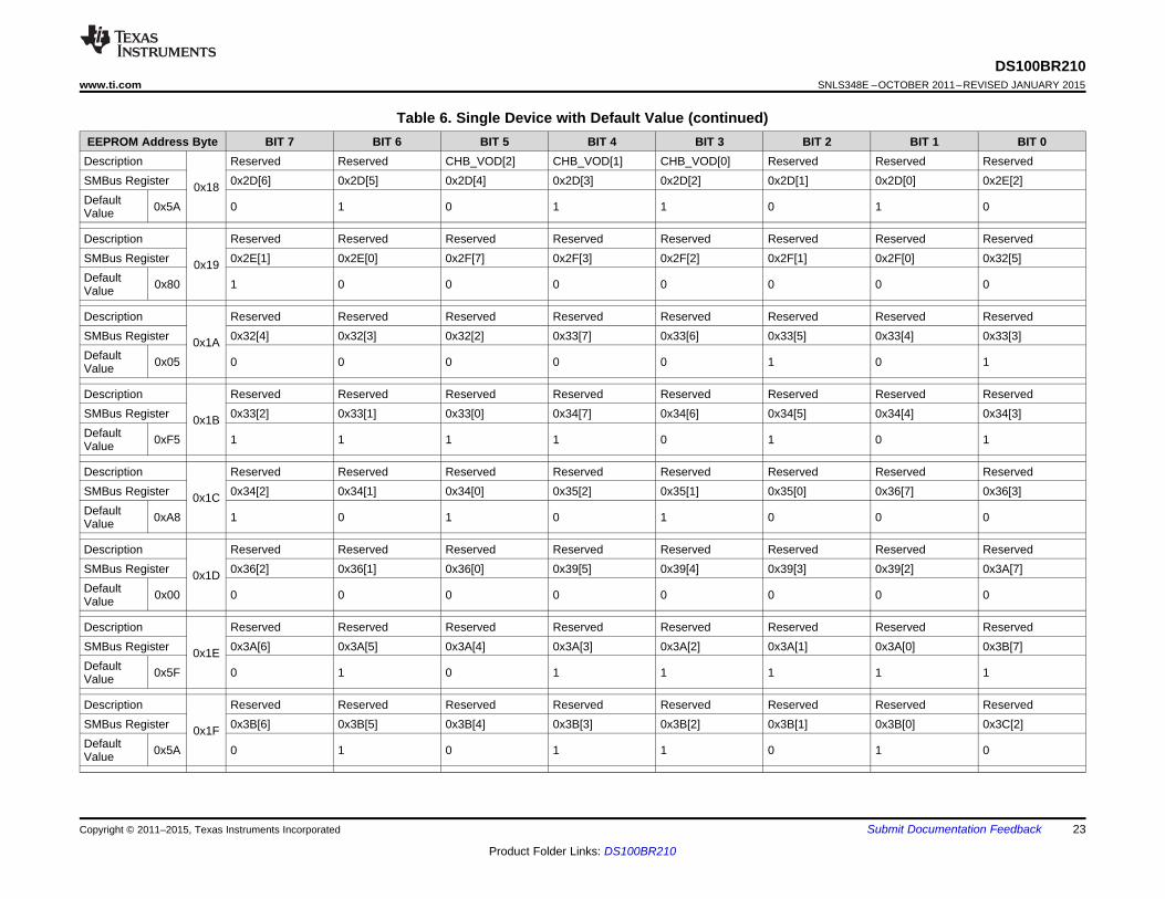
8.5.6.2 EEPROM Address MappingA detailed EEPROM Address Mapping for a single device is shown in Table 6. For instances where multipledevices are written to EEPROM, the device starting address definitions align starting with Byte 0x03. A registermap overview for a multi-device EEPROM address map is shown in Table 7.
Copyright © 2011–2015, Texas Instruments Incorporated Submit Documentation Feedback 19
Product Folder Links: DS100BR210

DS100BR210SNLS348E –OCTOBER 2011–REVISED JANUARY 2015 www.ti.com
Table 6. Single Device with Default ValueEEPROM Address Byte BIT 7 BIT 6 BIT 5 BIT 4 BIT 3 BIT 2 BIT 1 BIT 0
Address Map EEPROM > 256 DEVICE DEVICE DEVICE DEVICEDescription CRC_EN ReservedPresent Bytes COUNT[3] COUNT[2] COUNT[1] COUNT[0]0x00
Default 0x00 0 0 0 0 0 0 0 0Value
Description Reserved Reserved Reserved Reserved Reserved Reserved Reserved Reserved0x01Default 0x00 0 0 0 0 0 0 0 0Value
Max EEPROM Max EEPROM Max EEPROM Max EEPROM Max EEPROM Max EEPROM Max EEPROM Max EEPROMDescription Burst size[7] Burst size[6] Burst size[5] Burst size[4] Burst size[3] Burst size[2] Burst size[1] Burst size[0]0x02
Default 0x00 0 0 0 0 0 0 0 0Value
Cont_talk_EN_CH Cont_talk_EN_CHDescription Reserved Reserved Reserved Sel_LOS Reserved ReservedA BSMBus Register 0x03 0x01[7] 0x01[6] 0x01[5] 0x01[4] 0x01[3] 0x01[2] 0x01[1] 0x01[0]Default 0x00 0 0 0 0 0 0 0 0Value
Description Ovrd_LOS LOS_Value PWDN_Inputs PWDN_Osc Reserved eSATA En CHA eSATA En CHB Ovrd TX_DISSMBus Register 0x02[5] 0x02[4] 0x02[3] 0x02[2] 0x02[0] 0x04[7] 0x04[6] 0x04[5]0x04Default 0x00 0 0 0 0 0 0 0 0Value
Description TX_DIS CHA TX_DIS CHB Reserved EQ Stage 4 CHB EQ Stage 4 CHA Reserved Ovrd IDLE_TH ReservedSMBus Register 0x04[4] 0x04[3] 0x04[2] 0x04[1] 0x04[0] 0x06[4] 0x08[6] 0x08[5]0x05Default 0x04 0 0 0 0 0 1 0 0Value
Description Ovrd IDLE Reserved Ovrd Out_Mode Ovrd DEM Reserved Reserved Reserved ReservedSMBus Register 0x08[4] 0x08[3] 0x08[2] 0x08[1] 0x08[0] 0x0B[6] 0x0B[5] 0x0B[4]0x06Default 0x07 0 0 0 0 0 1 1 1Value
Description Reserved Reserved Reserved Reserved CHA_Idle_Auto CHA_Idle_Sel Reserved ReservedSMBus Register 0x0B[3] 0x0B[2] 0x0B[1] 0x0B[0] 0x0E[5] 0x0E[4] 0x0E[3] 0x0E[2]0x07Default 0x00 0 0 0 0 0 0 0 0Value
20 Submit Documentation Feedback Copyright © 2011–2015, Texas Instruments Incorporated
Product Folder Links: DS100BR210

DS100BR210www.ti.com SNLS348E –OCTOBER 2011–REVISED JANUARY 2015
Table 6. Single Device with Default Value (continued)EEPROM Address Byte BIT 7 BIT 6 BIT 5 BIT 4 BIT 3 BIT 2 BIT 1 BIT 0
Description CHA_EQ[7] CHA_EQ[6] CHA_EQ[5] CHA_EQ[4] CHA_EQ[3] CHA_EQ[2] CH0_EQ[1] CH0_EQ[0]SMBus Register 0x0F[7] 0x0F[6] 0x0F[5] 0x0F[4] 0x0F[3] 0x0F[2] 0x0F[1] 0x0F[0]0x08Default 0x2F 0 0 1 0 1 1 1 1Value
Description CHA_Sel SCP CHA_Out Mode Reserved Reserved Reserved Reserved Reserved ReservedSMBus Register 0x10[7] 0x10[6] 0x10[5] 0x10[4] 0x10[3] 0x10[2] 0x10[1] 0x10[0]0x09Default 0xED 1 1 1 0 1 1 0 1Value
Description CHA_DEM[2] CHA_DEM[1] CHA_DEM[0] Reserved CHA_Idle_ThA[1] CHA_Idle_ThA[0] CHA_Idle_ThD[1] CHA_Idle_ThD[0]SMBus Register 0x11[2] 0x11[1] 0x11[0] 0x12[7] 0x12[3] 0x12[2] 0x12[1] 0x12[0]0x0ADefault 0x40 0 1 0 0 0 0 0 0Value
Description CHB_Idle_Auto CHB_Idle_Sel Reserved Reserved CHB_EQ[7] CHB_EQ[6] CHB_EQ[5] CHB_EQ[4]SMBus Register 0x15[5] 0x15[4] 0x15[3] 0x15[2] 0x16[7] 0x16[6] 0x16[5] 0x16[4]0x0BDefault 0x02 0 0 0 0 0 0 1 0Value
Description CHB_EQ[3] CHB_EQ[2] CHB_EQ[1] CHB_EQ[0] CHB_Sel SCP CHB_Out Mode Reserved ReservedSMBus Register 0x16[3] 0x16[2] 0x16[1] 0x16[0] 0x17[7] 0x17[6] 0x17[5] 0x17[4]0x0CDefault 0xFE 1 1 1 1 1 1 1 0Value
Description Reserved Reserved Reserved Reserved CHB_DEM[2] CHB_DEM[1] CHB_DEM[0] ReservedSMBus Register 0x17[3] 0x17[2] 0x17[1] 0x17[0] 0x18[2] 0x18[1] 0x18[0] 0x19[7]0x0DDefault 0xD4 1 1 0 1 0 1 0 0Value
Description CHB_Idle_ThA[1] CHB_Idle_ThA[0] CHB_Idle_ThD[1] CHB_Idle_ThD[0] Reserved Reserved Reserved ReservedSMBus Register 0x19[3] 0x19[2] 0x19[1] 0x19[0] 0x1C[5] 0x1C[4] 0x1C[3] 0x1C[2]0x0EDefault 0x00 0 0 0 0 0 0 0 0Value
Description Reserved Reserved Reserved Reserved Reserved Reserved Reserved ReservedSMBus Register 0x1D[7] 0x1D[6] 0x1D[5] 0x1D[4] 0x1D[3] 0x1D[2] 0x1D[1] 0x1D[0]0x0FDefault 0x2F 0 0 1 0 1 1 1 1Value
Copyright © 2011–2015, Texas Instruments Incorporated Submit Documentation Feedback 21
Product Folder Links: DS100BR210

DS100BR210SNLS348E –OCTOBER 2011–REVISED JANUARY 2015 www.ti.com
Table 6. Single Device with Default Value (continued)EEPROM Address Byte BIT 7 BIT 6 BIT 5 BIT 4 BIT 3 BIT 2 BIT 1 BIT 0
Description Reserved Reserved Reserved Reserved Reserved Reserved Reserved ReservedSMBus Register 0x1E[7] 0x1E[6] 0x1E[5] 0x1E[4] 0x1E[3] 0x1E[2] 0x1E[1] 0x1E[0]0x10Default 0xAD 1 0 1 0 1 1 0 1Value
Description Reserved Reserved Reserved Reserved Reserved Reserved Reserved ReservedSMBus Register 0x1F[2] 0x1F[1] 0x1F[0] 0x20[7] 0x20[3] 0x20[2] 0x20[1] 0x20[0]0x11Default 0x40 0 1 0 0 0 0 0 0Value
Description Reserved Reserved Reserved Reserved Reserved Reserved Reserved ReservedSMBus Register 0x23[5] 0x23[4] 0x23[3] 0x23[2] 0x24[7] 0x24[6] 0x24[5] 0x24[4]0x12Default 0x02 0 0 0 0 0 0 1 0Value
Description Reserved Reserved Reserved Reserved Reserved Reserved Reserved CHA_VOD[2]SMBus Register 0x24[3] 0x24[2] 0x24[1] 0x24[0] 0x25[7] 0x25[6] 0x25[5] 0x25[4]0x13Default 0xFA 1 1 1 1 1 0 1 0Value
Description CHA_VOD[1] CHA_VOD[0] Reserved Reserved Reserved Reserved Reserved ReservedSMBus Register 0x25[3] 0x25[2] 0x25[1] 0x25[0] 0x26[2] 0x26[1] 0x26[0] 0x27[7]0x14Default 0xD4 1 1 0 1 0 1 0 0Value
Description Reserved Reserved Reserved Reserved Ovrd_Fast IDLE hi_idle_th_CHA hi_idle_th_CHB fast_idle_CHASMBus Register 0x27[3] 0x27[2] 0x27[1] 0x27[0] 0x28[6] 0x28[5] 0x28[4] 0x28[3]0x15Default 0x00 0 0 0 0 0 0 0 0Value
Description fast_idle_CHB Reserved Reserved Reserved Reserved Reserved Reserved ReservedSMBus Register 0x28[2] 0x28[1] 0x28[0] 0x2B[5] 0x2B[4] 0x2B[3] 0x2B[2] 0x2C[7]0x16Default 0x00 0 0 0 0 0 0 0 0Value
Description Reserved Reserved Reserved Reserved Reserved Reserved Reserved ReservedSMBus Register 0x2C[6] 0x2C[5] 0x2C[4] 0x2C[3] 0x2C[2] 0x2C[1] 0x2C[0] 0x2D[7]0x17Default 0x5F 0 1 0 1 1 1 1 1Value
22 Submit Documentation Feedback Copyright © 2011–2015, Texas Instruments Incorporated
Product Folder Links: DS100BR210
DS100BR210www.ti.com SNLS348E –OCTOBER 2011–REVISED JANUARY 2015
Table 6. Single Device with Default Value (continued)EEPROM Address Byte BIT 7 BIT 6 BIT 5 BIT 4 BIT 3 BIT 2 BIT 1 BIT 0
Description Reserved Reserved CHB_VOD[2] CHB_VOD[1] CHB_VOD[0] Reserved Reserved ReservedSMBus Register 0x2D[6] 0x2D[5] 0x2D[4] 0x2D[3] 0x2D[2] 0x2D[1] 0x2D[0] 0x2E[2]0x18Default 0x5A 0 1 0 1 1 0 1 0Value
Description Reserved Reserved Reserved Reserved Reserved Reserved Reserved ReservedSMBus Register 0x2E[1] 0x2E[0] 0x2F[7] 0x2F[3] 0x2F[2] 0x2F[1] 0x2F[0] 0x32[5]0x19Default 0x80 1 0 0 0 0 0 0 0Value
Description Reserved Reserved Reserved Reserved Reserved Reserved Reserved ReservedSMBus Register 0x32[4] 0x32[3] 0x32[2] 0x33[7] 0x33[6] 0x33[5] 0x33[4] 0x33[3]0x1ADefault 0x05 0 0 0 0 0 1 0 1Value
Description Reserved Reserved Reserved Reserved Reserved Reserved Reserved ReservedSMBus Register 0x33[2] 0x33[1] 0x33[0] 0x34[7] 0x34[6] 0x34[5] 0x34[4] 0x34[3]0x1BDefault 0xF5 1 1 1 1 0 1 0 1Value
Description Reserved Reserved Reserved Reserved Reserved Reserved Reserved ReservedSMBus Register 0x34[2] 0x34[1] 0x34[0] 0x35[2] 0x35[1] 0x35[0] 0x36[7] 0x36[3]0x1CDefault 0xA8 1 0 1 0 1 0 0 0Value
Description Reserved Reserved Reserved Reserved Reserved Reserved Reserved ReservedSMBus Register 0x36[2] 0x36[1] 0x36[0] 0x39[5] 0x39[4] 0x39[3] 0x39[2] 0x3A[7]0x1DDefault 0x00 0 0 0 0 0 0 0 0Value
Description Reserved Reserved Reserved Reserved Reserved Reserved Reserved ReservedSMBus Register 0x3A[6] 0x3A[5] 0x3A[4] 0x3A[3] 0x3A[2] 0x3A[1] 0x3A[0] 0x3B[7]0x1EDefault 0x5F 0 1 0 1 1 1 1 1Value
Description Reserved Reserved Reserved Reserved Reserved Reserved Reserved ReservedSMBus Register 0x3B[6] 0x3B[5] 0x3B[4] 0x3B[3] 0x3B[2] 0x3B[1] 0x3B[0] 0x3C[2]0x1FDefault 0x5A 0 1 0 1 1 0 1 0Value
Copyright © 2011–2015, Texas Instruments Incorporated Submit Documentation Feedback 23
Product Folder Links: DS100BR210

DS100BR210SNLS348E –OCTOBER 2011–REVISED JANUARY 2015 www.ti.com
Table 6. Single Device with Default Value (continued)EEPROM Address Byte BIT 7 BIT 6 BIT 5 BIT 4 BIT 3 BIT 2 BIT 1 BIT 0
Description Reserved Reserved Reserved Reserved Reserved Reserved Reserved ReservedSMBus Register 0x3C[1] 0x3C[0] 0x3D[7] 0x3D[3] 0x3D[2] 0x3D[1] 0x3D[0] 0x40[5]0x20Default 0x80 1 0 0 0 0 0 0 0Value
Description Reserved Reserved Reserved Reserved Reserved Reserved Reserved ReservedSMBus Register 0x40[4] 0x40[3] 0x40[2] 0x41[7] 0x41[6] 0x41[5] 0x41[4] 0x41[3]0x21Default 0x05 0 0 0 0 0 1 0 1Value
Description Reserved Reserved Reserved Reserved Reserved Reserved Reserved ReservedSMBus Register 0x41[2] 0x41[1] 0x41[0] 0x42[7] 0x42[6] 0x42[5] 0x42[4] 0x42[3]0x22Default 0xF5 1 1 1 1 0 1 0 1Value
Description Reserved Reserved Reserved Reserved Reserved Reserved Reserved ReservedSMBus Register 0x42[2] 0x42[1] 0x42[0] 0x43[2] 0x43[1] 0x43[0] 0x44[7] 0x44[3]0x23Default 0xA8 1 0 1 0 1 0 0 0Value
Description Reserved Reserved Reserved Reserved Reserved Reserved Reserved ReservedSMBus Register 0x44[2] 0x44[1] 0x44[0] 0x47[3] 0x47[2] 0x47[1] 0x47[0] 0x48[7]0x24Default 0x00 0 0 0 0 0 0 0 0Value
Description Reserved Reserved Reserved Reserved Reserved Reserved Reserved ReservedSMBus Register 0x48[6] 0x4C[7] 0x4C[6] 0x4C[5] 0x4C[4] 0x4C[3] 0x4C[0] 0x59[0]0x25Default 0x00 0 0 0 0 0 0 0 0Value
Description Reserved Reserved Reserved Reserved Reserved Reserved Reserved ReservedSMBus Register 0x5A[7] 0x5A[6] 0x5A[5] 0x5A[4] 0x5A[3] 0x5A[2] 0x5A[1] 0x5A[0]0x26Default 0x54 0 1 0 1 0 1 0 0Value
Description Reserved Reserved Reserved Reserved Reserved Reserved Reserved ReservedSMBus Register 0x5B[7] 0x5B[6] 0x5B[5] 0x5B[4] 0x5B[3] 0x5B[2] 0x5B[1] 0x5B[0]0x27Default 0x54 0 1 0 1 0 1 0 0Value
24 Submit Documentation Feedback Copyright © 2011–2015, Texas Instruments Incorporated
Product Folder Links: DS100BR210

DS100BR210www.ti.com SNLS348E –OCTOBER 2011–REVISED JANUARY 2015
Table 7. Multi-Device EEPROM Address Map Overview (1)
ADDR BIT 7 BIT 6 BIT 5 BIT 4 BIT 3 BIT 2 BIT 1 BIT 0
0 CRC EN Address Map EEPROM > 256 Reserved COUNT[3] COUNT[2] COUNT[1] COUNT[0]Bytes
Header 1 Reserved Reserved Reserved Reserved Reserved Reserved Reserved Reserved2 EE Burst[7] EE Burst[6] EE Burst[5] EE Burst[4] EE Burst[3] EE Burst[2] EE Burst[1] EE Burst[0]
Device 0 3 CRC[7] CRC[6] CRC[5] CRC[4] CRC[3] CRC[2] CRC[1] CRC[0]Info 4 EE AD0 [7] EE AD0 [6] EE AD0 [5] EE AD0 [4] EE AD0 [3] EE AD0 [2] EE AD0 [1] EE AD0 [0]Device 1 5 CRC[7] CRC[6] CRC[5] CRC[4] CRC[3] CRC[2] CRC[1] CRC[0]Info 6 EE AD1 [7] EE AD1 [6] EE AD1 [5] EE AD1 [4] EE AD1 [3] EE AD1 [2] EE AD1 [1] EE AD1 [0]Device 2 7 CRC[7] CRC[6] CRC[5] CRC[4] CRC[3] CRC[2] CRC[1] CRC[0]Info 8 EE AD2 [7] EE AD2 [6] EE AD2 [5] EE AD2 [4] EE AD2 [3] EE AD2 [2] EE AD2 [1] EE AD2 [0]Device 3 9 CRC[7] CRC[6] CRC[5] CRC[4] CRC[3] CRC[2] CRC[1] CRC[0]Info 10 EE AD3 [7] EE AD3 [6] EE AD3 [5] EE AD3 [4] EE AD3 [3] EE AD3 [2] EE AD3 [1] EE AD3 [0]
Device 0 11 RES RES RES RES RES Sel_LOS RES RESAddr 3Device 0 12 Ovrd_LOS LOS_Value PWDN Inp PWDN OSC RES eSATA CHA eSATA CHB Ovrd TX_DISAddr 4Device 0 46 RES RES RES RES RES RES RES RESAddr 38Device 0 47 RES RES RES RES RES RES RES RESAddr 39
Device 1 48 RES RES RES RES RES Sel_LOS RES RESAddr 3Device 1 49 Ovrd_LOS LOS_Value PWDN Inp PWDN OSC RES eSATA CHA eSATA CHB Ovrd TX_DISAddr 4Device 1 83 RES RES RES RES RES RES RES RESAddr 38Device 1 84 RES RES RES RES RES RES RES RESAddr 39
Device 2 85 RES RES RES RES RES Sel_LOS RES RESAddr 3Device 2 86 Ovrd_LOS LOS_Value PWDN Inp PWDN OSC RES eSATA CHA eSATA CHB Ovrd TX_DISAddr 4
(1) (a) CRC EN = 1; Address Map = 1(b) EEPROM > 256 Bytes = 0(c) COUNT[3:0] = 0011'b(d) Note: Multiple DS100BR210 devices may point at the same address space if they have identical programming values.
Copyright © 2011–2015, Texas Instruments Incorporated Submit Documentation Feedback 25
Product Folder Links: DS100BR210

DS100BR210SNLS348E –OCTOBER 2011–REVISED JANUARY 2015 www.ti.com
Table 7. Multi-Device EEPROM Address Map Overview(1) (continued)ADDR BIT 7 BIT 6 BIT 5 BIT 4 BIT 3 BIT 2 BIT 1 BIT 0
Device 2 120 RES RES RES RES RES RES RES RESAddr 38Device 2 121 RES RES RES RES RES RES RES RESAddr 39
Device 3 122 RES RES RES RES RES Sel_LOS RES RESAddr 3Device 3 123 Ovrd_LOS LOS_Value PWDN Inp PWDN OSC RES eSATA CHA eSATA CHB Ovrd TX_DISAddr 4Device 3 157 RES RES RES RES RES RES RES RESAddr 38Device 3 158 RES RES RES RES RES RES RES RESAddr 39
26 Submit Documentation Feedback Copyright © 2011–2015, Texas Instruments Incorporated
Product Folder Links: DS100BR210
DS100BR210www.ti.com SNLS348E –OCTOBER 2011–REVISED JANUARY 2015
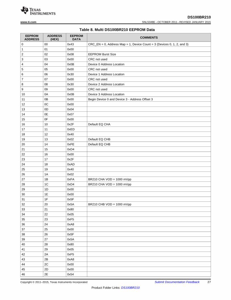
Table 8. Multi DS100BR210 EEPROM DataEEPROM ADDRESS EEPROM COMMENTSADDRESS (HEX) DATA
0 00 0x43 CRC_EN = 0, Address Map = 1, Device Count = 3 (Devices 0, 1, 2, and 3)1 01 0x002 02 0x08 EEPROM Burst Size3 03 0x00 CRC not used4 04 0x0B Device 0 Address Location5 05 0x00 CRC not used6 06 0x30 Device 1 Address Location7 07 0x00 CRC not used8 08 0x30 Device 2 Address Location9 09 0x00 CRC not used10 0A 0x0B Device 3 Address Location11 0B 0x00 Begin Device 0 and Device 3 - Address Offset 312 0C 0x0013 0D 0x0414 0E 0x0715 0F 0x0016 10 0x2F Default EQ CHA17 11 0xED18 12 0x4019 13 0x02 Default EQ CHB20 14 0xFE Default EQ CHB21 15 0xD422 16 0x0023 17 0x2F24 18 0xAD25 19 0x4026 1A 0x0227 1B 0xFA BR210 CHA VOD = 1000 mVpp28 1C 0xD4 BR210 CHA VOD = 1000 mVpp29 1D 0x0030 1E 0x0031 1F 0x5F32 20 0x5A BR210 CHB VOD = 1000 mVpp33 21 0x8034 22 0x0535 23 0xF536 24 0xA837 25 0x0038 26 0x5F39 27 0x5A40 28 0x8041 29 0x0542 2A 0xF543 2B 0xA844 2C 0x0045 2D 0x0046 2E 0x54
Copyright © 2011–2015, Texas Instruments Incorporated Submit Documentation Feedback 27
Product Folder Links: DS100BR210

DS100BR210SNLS348E –OCTOBER 2011–REVISED JANUARY 2015 www.ti.com
Table 8. Multi DS100BR210 EEPROM Data (continued)EEPROM ADDRESS EEPROM COMMENTSADDRESS (HEX) DATA
47 2F 0x54 End Device 0 and Device 3 - Address Offset 3948 30 0x00 Begin Device 1 and Device 2 - Address Offset 349 31 0x0050 32 0x0451 33 0x0752 34 0x0053 35 0x2F Default EQ CHA54 36 0xED55 37 0x4056 38 0x02 Default EQ CHB57 39 0xFE Default EQ CHB58 3A 0xD459 3B 0x0060 3C 0x2F61 3D 0xAD62 3E 0x4063 3F 0x0264 40 0xFA BR210 CHA VOD = 1000 mVpp65 41 0xD4 BR210 CHA VOD = 1000 mVpp66 42 0x0067 43 0x0068 44 0x5F69 45 0x5A BR210 CHB VOD = 1000 mVpp70 46 0x8071 47 0x0572 48 0xF573 49 0xA874 4A 0x0075 4B 0x5F76 4C 0x5A77 4D 0x8078 4E 0x0579 4F 0xF580 50 0xA881 51 0x0082 52 0x0083 53 0x5484 54 0x54 End Device 1 and Device 2 - Address Offset 39
28 Submit Documentation Feedback Copyright © 2011–2015, Texas Instruments Incorporated
Product Folder Links: DS100BR210

DS100BR210www.ti.com SNLS348E –OCTOBER 2011–REVISED JANUARY 2015
8.6 Register Maps
Table 9. SMBus Slave Mode Register MapREGISTER EEPROMADDRESS BIT FIELD TYPE DEFAULT DESCRIPTIONNAME REG BIT
7 Reserved R/W Set bit to 0SMBus Address6:3 R SMBus strap observation[3:0]
0x00 Device ID 0x00EEPROM Reading 1 = EEPROM Done Loading2 RDone 0 = EEPROM Loading
1:0 Reserved RWSC Set bits to 0Continuous Talk Control (Output Always On)
7:6 Idle Control [7]: Continuous talk ENABLE (Channel A)[6]: Continuous talk ENABLE (Channel B)
5:3 Reserved Set bits to 00x01 Control 1 R/W 0x00 Yes
LOS Monitor Selection2 LOS Select 1 = Use LOS from CH B
0 = Use LOS from CH A1:0 Reserved Set bits to 07:6 Reserved Set bits to 0
1 = LOS pin override enable5 LOS override Yes 0 = Use Normal Signal Detection1 = Normal Operation4 LOS override value Yes 0 = Output LOS0x02 Control 2 R/W 0x00
3 PWDN Inputs Yes 1 = PWDN0 = Normal Operation2 PWDN Oscillator Yes
1 Reserved Set bit to 00 Reserved Yes Set bit to 0
0x03 Reserved 7:0 Reserved R/W 0x00 ReservedeSATA Mode [7] Channel A (1)7:6 Enable [6] Channel B (1)TX_DIS Override 1 = Override Use Reg 0x04[4:3]5 Enable 0 = Normal Operation - uses pinTX_DIS Value 1 = Channel A TX Disabled4 Channel A 0 = Channel A TX EnabledTX_DIS Value 1 = Channel B TX Disabled3 Channel B 0 = Channel B TX Enabled
0x04 Control 3 R/W 0x00 Yes2 Reserved Set bit to 0[1]: Channel B - EQ Stage 4 Limiting On/Off[0]: Channel A - EQ Stage 4 Limiting On/OffSetting this control bit turns on added voltagegain compared to normal operating range. If theEQ Stage 41:0 bits are set to 1 (On), the EQ will act as aLimiting Control limiting amplifier, resulting in reduction ofoverall linear gain characteristics. Turning thesebits On is not recommended for 10G-KRapplications.
0x05 Reserved 7:0 Reserved R/W 0x00 Reserved
Copyright © 2011–2015, Texas Instruments Incorporated Submit Documentation Feedback 29
Product Folder Links: DS100BR210

DS100BR210SNLS348E –OCTOBER 2011–REVISED JANUARY 2015 www.ti.com
Register Maps (continued)Table 9. SMBus Slave Mode Register Map (continued)
REGISTER EEPROMADDRESS BIT FIELD TYPE DEFAULT DESCRIPTIONNAME REG BITDisable EEPROM7 Disable Master Mode EEPROM ConfigurationCFG
6:5 Reserved Set bits to 04 Reserved Yes Set bit to 1
1 = Enable SMBus Slave Mode RegisterSlave Control
0x06 Register R/W 0x10 0 = Disable SMBus Slave Mode RegisterControl 3 Register Enable Control
Note: In order to change VOD, DEM, and EQof the channels in slave mode, this bit mustbe set to 1.
2:1 Reserved Set bits to 00 Reserved Set bit to 07 Reserved Set bit to 0
1 = Self clearing reset for SMBus registers6 Reset Registers (register settings return to default values)Digital Reset0x07 R/W 0x01and Control Reset SMBus 1 = Self clearing reset to SMBus master state5 Master machine4:0 Reserved Set bits to 0 0001'b7 Reserved Set bit to 0
1 = Override by Channel - see Reg 0x13 andOverride Idle6 Yes 0x19Threshold 0 = SD_TH pin control5 Reserved Yes Set bit to 0
1 = Force IDLE by Channel - see Reg 0x0E4 Override IDLE Yes and 0x15
0 = Normal OperationSet bit to 0Note: For all applications operating > 8Gbps,3 Reserved0x08 Pin Override R/W 0x00 users must set this bit to 1 and enable allchannels manually.
1 = Enable Output Mode control for individualYesoutputs. See register locations 0x10[6] and
Override Output 0x17[6].2 Mode 0 = Disable - Outputs are kept in the normalmode of operation allowing VOD and DEadjustments.
1 Override DEM Yes Override De-emphasis (ignore rate)0 Reserved Yes Set bit to 0
0x09-0x0A Reserved 7:0 Reserved R/W 0x00 Reserved7 Reserved Reserved
0x0B Reserved R/W 0x706:0 Reserved Yes Reserved
CH A0x0C Analog 7:0 Reserved R/W 0x00 Set bits to 0x00
Override 1CH A0x0D 7:0 Reserved R/W 0x00 Set bits to 0x00.Reserved
30 Submit Documentation Feedback Copyright © 2011–2015, Texas Instruments Incorporated
Product Folder Links: DS100BR210

DS100BR210www.ti.com SNLS348E –OCTOBER 2011–REVISED JANUARY 2015
Register Maps (continued)Table 9. SMBus Slave Mode Register Map (continued)
REGISTER EEPROMADDRESS BIT FIELD TYPE DEFAULT DESCRIPTIONNAME REG BIT7:6 Reserved Set bits to 0
1 = Allow IDLE Select control in bit 40 = Automatic IDLE detect5 Idle Auto Yes (Must set 0x08[4] = 1 to override pin-selectcontrol)
CH A0x0E R/W 0x00 1 = Output is muted (electrical IDLE)Idle Control 0 = Output is on4 Idle Select Yes (Must set 0x08[4] = 1 to override pin-selectcontrol)
3:2 Reserved Yes Set bits to 01:0 Reserved Set bits to 0
CH A EQ Boost Default to 24 dB0x0F 7:0 BOOST [7:0] R/W 0x2F YesEQ Setting See Table 3 for Information1 = Short Circuit Protection ON7 Sel_scp Yes 0 = Short Circuit Protection OFF1 = Normal operationCH A 6 Output Mode Yes0x10 R/W 0xED 0 = 10G-KR operationControl 1
5:3 Reserved Yes Set bits to 101'b2:0 Reserved Yes Set bits to 101'b7:5 Reserved R Set bits to 100'b4:3 Reserved Set bits to 0
De-Emphasis000'b = -0.0 dB001'b = -1.5 dBCH A0x11 0x82 010'b = -3.5 dB (Default)Control 2 R/W
2:0 DEM [2:0] Yes 011'b = -6.0 dB100'b = -8.0 dB101'b = -9.0 dB110'b = -10.5 dB111'b = -12.0 dB
7 Reserved Yes Set bit to 06:4 Reserved Set bits to 0
Assert ThresholdsUse only if register 0x08 [6] = 1
IDLE Assert 00'b = 180 mVpp (Default)3:2 YesThreshold[1:0] 01'b = 160 mVppCH A10'b = 210 mVpp0x12 Idle R/W 0x0011'b = 190 mVppThresholdDe-assert ThresholdsUse only if register 0x08 [6] = 1
IDLE De-assert 00'b = 110 mVpp (Default)1:0 YesThreshold[1:0] 01'b = 100 mVpp10'b = 150 mVpp11'b = 130 mVpp
CH B0x13 Analog 7:0 Reserved R/W 0x00 Set bits to 0x00
Override 1CH B0x14 7:0 Reserved R/W 0x00 Set bits to 0x00Reserved
Copyright © 2011–2015, Texas Instruments Incorporated Submit Documentation Feedback 31
Product Folder Links: DS100BR210

DS100BR210SNLS348E –OCTOBER 2011–REVISED JANUARY 2015 www.ti.com
Register Maps (continued)Table 9. SMBus Slave Mode Register Map (continued)
REGISTER EEPROMADDRESS BIT FIELD TYPE DEFAULT DESCRIPTIONNAME REG BIT7:6 Reserved Set bits to 0
1 = Allow IDLE Select control in bit 40 = Automatic IDLE detect5 Idle Auto Yes (Must set 0x08[4] = 1 to override pin-selectcontrol)
CH B0x15 R/W 0x00 1 = Output is muted (electrical IDLE)Idle Control 0 = Output is on4 Idle Select Yes (Must set 0x08[4] = 1 to override pin-selectcontrol)
3:2 Reserved Yes Set bits to 01:0 Reserved Set bits to 0
CH B EQ Boost Default to 24 dB0x16 7:0 BOOST [7:0] R/W 0x2F YesEQ Setting See Table 3 for Information1 = Short Circuit Protection ON7 Sel_scp Yes 0 = Short Circuit Protection OFF1 = Normal operationCH B 6 Output Mode Yes0x17 R/W 0xED 0 = 10G-KR operationControl 1
5:3 Reserved Yes Set bits to 101'b2:0 Reserved Yes Set bits to 101'b7:5 Reserved R Set bits to 100'b4:3 Reserved Set bits to 0
De-Emphasis (Default = -3.5 dB)000'b = -0.0 dB001'b = -1.5 dBCH B0x18 0x82 010'b = -3.5 dBControl 2 R/W
2:0 DEM [2:0] Yes 011'b = -6.0 dB100'b = -8.0 dB101'b = -9.0 dB110'b = -10.5 dB111'b = -12.0 dB
7 Reserved Yes Set bit to 06:4 Reserved Set bits to 0
Assert ThresholdsUse only if register 0x08 [6] = 1
IDLE Assert 00'b = 180 mVpp (Default)3:2 YesThreshold[1:0] 01'b = 160 mVppCH B10'b = 210 mVpp0x19 Idle R/W 0x0011'b = 190 mVppThresholdDe-assert ThresholdsUse only if register 0x08 [6] = 1
IDLE De-assert 00'b = 110 mVpp (Default)1:0 YesThreshold[1:0] 01'b = 100 mVpp10'b = 150 mVpp11'b = 130 mVpp
0x1A-0x1B Reserved 7:0 Reserved R/W 0x00 Reserved7:6 Reserved Reserved
0x1C Reserved 5:2 Reserved R/W 0x00 Yes Reserved1:0 Reserved Reserved
0x1D Reserved 7:0 Reserved R/W 0x2F Yes Reserved0x1E Reserved 7:0 Reserved R/W 0xAD Yes Reserved
7:3 Reserved Reserved0x1F Reserved R/W 0x02
2:0 Reserved Yes Reserved
32 Submit Documentation Feedback Copyright © 2011–2015, Texas Instruments Incorporated
Product Folder Links: DS100BR210

DS100BR210www.ti.com SNLS348E –OCTOBER 2011–REVISED JANUARY 2015
Register Maps (continued)Table 9. SMBus Slave Mode Register Map (continued)
REGISTER EEPROMADDRESS BIT FIELD TYPE DEFAULT DESCRIPTIONNAME REG BIT7 Reserved Yes Reserved
0x20 Reserved 6:4 Reserved R/W 0x00 Reserved3:0 Reserved Yes Reserved
0x21-0x22 Reserved 7:0 Reserved R/W 0x00 Reserved7:6 Reserved Set bits to 0
0x23 Reserved 5:2 Reserved R/W 0x00 Yes Set bits to 01:0 Reserved Set bits to 0
0x24 Reserved 7:0 Reserved R/W 0x2F Yes Reserved7:5 Reserved Yes Set bits to 0
VOD Controls for CH A000'b = 700 mVpp001'b = 800 mVpp
CH A VOD 010'b = 900 mVpp0x25 4:2 VOD_CHA[2:0] R/W 0xAD YesControl 011'b = 1000 mVpp (Default)100'b = 1100 mVpp101'b = 1200 mVpp110'b = 1300 mVpp
1:0 Reserved Yes Set bits to 07:3 Reserved Reserved
0x26 Reserved R/W 0x022:0 Reserved Yes Reserved7 Reserved Yes Reserved
0x27 Reserved 6:4 Reserved R/W 0x00 Reserved3:0 Reserved Yes Reserved7 Reserved Set bit to 0
1 = Enable Fast IDLE control in Reg 0x28[3:2]6 Override Fast Idle Yes 0 = Disable Fast IDLE control in Reg 0x28[3:2].Enable high SD thresholds (Slow IDLE)
5:4 en_hi_idle_th[1:0] Yes [5]: CH A0x28 Idle Control R/W 0x00 [4]: CH BEnable Fast IDLE
3:2 en_fast_idle[1:0] Yes [3]: CH A[2]: CH B
1:0 Reserved Yes Set bits to 00x29-0x2A Reserved 7:0 Reserved R/W 0x00 Reserved
7:6 Reserved Reserved0x2B Reserved 5:2 Reserved R/W 0x00 Yes Reserved
1:0 Reserved Reserved0x2C Reserved 7:0 Reserved R/W 0x2F Yes Reserved
7:5 Reserved Yes Set bits to 101'bVOD Controls for CH B000'b = 700 mVpp001'b = 800 mVpp
CH B VOD 010'b = 900 mVpp0x2D 4:2 VOD_CHB[2:0] R/W 0xAD YesControl 011'b = 1000 mVpp (Default)100'b = 1100 mVpp101'b = 1200 mVpp110'b = 1300 mVpp
1:0 Reserved Yes Set bits to 01'b7:3 Reserved Reserved
0x2E Reserved R/W 0x022:0 Reserved Yes Reserved
Copyright © 2011–2015, Texas Instruments Incorporated Submit Documentation Feedback 33
Product Folder Links: DS100BR210

DS100BR210SNLS348E –OCTOBER 2011–REVISED JANUARY 2015 www.ti.com
Register Maps (continued)Table 9. SMBus Slave Mode Register Map (continued)
REGISTER EEPROMADDRESS BIT FIELD TYPE DEFAULT DESCRIPTIONNAME REG BIT7 Reserved Yes Reserved
0x2F Reserved 6:4 Reserved R/W 0x00 Reserved3:0 Reserved Yes Reserved
0x30-0x31 Reserved 7:0 Reserved R/W 0x00 Reserved7:6 Reserved Reserved
0x32 Reserved 5:2 Reserved R/W 0x00 Yes Reserved1:0 Reserved Reserved
0x33 Reserved 7:0 Reserved R/W 0x2F Yes Reserved0x34 Reserved 7:0 Reserved R/W 0xAD Yes Reserved
7:3 Reserved Reserved0x35 Reserved R/W 0x02
2:0 Reserved Yes Reserved7 Reserved Yes Reserved
0x36 Reserved 6:4 Reserved R/W 0x00 Reserved3:0 Reserved Yes Reserved
0x37-0x38 Reserved 7:0 Reserved R/W 0x00 Reserved7:6 Reserved Reserved
0x39 Reserved 5:2 Reserved R/W 0x00 Yes Reserved1:0 Reserved Reserved
0x3A Reserved 7:0 Reserved R/W 0x2F Yes Reserved0x3B Reserved 7:0 Reserved R/W 0xAD Yes Reserved
7:3 Reserved Reserved0x3C Reserved R/W 0x02
2:0 Reserved Yes Reserved7 Reserved Yes Reserved
0x3D Reserved 6:4 Reserved R/W 0x00 Reserved3:0 Reserved Yes Reserved
0x3E-0x3F Reserved 7:0 Reserved R/W 0x00 Reserved7:6 Reserved Reserved
0x40 Reserved 5:2 Reserved R/W 0x00 Yes Reserved1:0 Reserved Reserved
0x41 Reserved 7:0 Reserved R/W 0x2F Yes Reserved0x42 Reserved 7:0 Reserved R/W 0xAD Yes Reserved
7:3 Reserved Reserved0x43 Reserved R/W 0x02
2:0 Reserved Yes Reserved7 Reserved Yes Reserved
0x44 Reserved 6:4 Reserved R/W 0x00 Reserved3:0 Reserved Yes Reserved
0x45 Reserved 7:0 Reserved R/W 0x00 Reserved0x46 Reserved 7:0 Reserved R/W 0x38 Reserved
7:4 Reserved Reserved0x47 Reserved R/W 0x00
3:0 Reserved Yes Reserved7:6 Reserved Yes Reserved
0x48 Reserved R/W 0x055:0 Reserved Reserved
0x49-0x4B Reserved 7:0 Reserved R/W 0x00 Reserved
34 Submit Documentation Feedback Copyright © 2011–2015, Texas Instruments Incorporated
Product Folder Links: DS100BR210

DS100BR210www.ti.com SNLS348E –OCTOBER 2011–REVISED JANUARY 2015
Register Maps (continued)Table 9. SMBus Slave Mode Register Map (continued)
REGISTER EEPROMADDRESS BIT FIELD TYPE DEFAULT DESCRIPTIONNAME REG BIT7:3 Reserved Yes Reserved
0x4C Reserved 2:1 Reserved R/W 0x00 Reserved0 Reserved Yes Reserved
0x4D-0x50 Reserved 7:0 Reserved R/W 0x00 Reserved7:5 Version 011'bDevice0x51 R 0x66Information 4:0 Device ID 0 0110'b
0x52-0x55 Reserved 7:0 Reserved R/W 0x00 Reserved0x56 Reserved 7:0 Reserved R/W 0x02 Reserved0x57 Reserved 7:0 Reserved R/W 0x14 Reserved0x58 Reserved 7:0 Reserved R/W 0x21 Reserved
7:1 Reserved Reserved0x59 Reserved R/W 0x00
0 Reserved Yes Reserved0x5A Reserved 7:0 Reserved R/W 0x54 Yes Reserved0x5B Reserved 7:0 Reserved R/W 0x54 Yes Reserved
0x5C-0x61 Reserved 7:0 Reserved R/W 0x00 Reserved
Copyright © 2011–2015, Texas Instruments Incorporated Submit Documentation Feedback 35
Product Folder Links: DS100BR210

DS100BR210SNLS348E –OCTOBER 2011–REVISED JANUARY 2015 www.ti.com
9 Application and Implementation
NOTEInformation in the following applications sections is not part of the TI componentspecification, and TI does not warrant its accuracy or completeness. TI’s customers areresponsible for determining suitability of components for their purposes. Customers shouldvalidate and test their design implementation to confirm system functionality.
9.1 Application Information
9.1.1 Signal Integrity in 10G-KR ApplicationsWhen configured in "KR Mode", using either the VOD_SEL and MODE pin setting or SMBus register control, theDS100BR210 is designed to operate transparently within a KR backplane channel environment. Installing aDS100BR210 repeater within the KR backplane channel splits the total channel attenuation into two parts. Inother words, operating in "KR Mode" implies that signals will pass through the repeater with a linearized output.Ideally the repeater can be placed near the middle of the channel, maximizing the signal-to-noise ratio across thebidirectional interface.
In order to maximize the 10G-KR solution space, the 802.3ap specification calls for an optimization of the Txpartner signal conditioning coefficients based on feedback from the KR Rx ASIC endpoint. This link optimizationsequence is commonly referred to as "link training" and is performed at speed (10.3125 Gbps). Setting theDS100BR210 active CTLE to compensate for the channel loss from each of the KR transmitters will reduce thetransmit and receive equalization settings required on the KR physical layer devices. This central location keepsa larger signal-to-noise ratio at all points in the channel, extending the available solution space and increasingthe overall margin of almost any channel. Suggested initial settings for the DS100BR210 are given in Table 10and Table 11. Further adjustments to EQx, DEMx, and VODx settings may optimize signal margin on the link fordifferent system applications.
Table 10. Suggested 10G-KR Initial Device Settings in Pin Mode (1)
CHANNEL SETTINGS PIN MODEEQx[1:0] 0, 0
VOD_SEL 1DEMx 0
(1) For 10G-KR mode with slow idle-to-active response, the MODE pin should be left floating.
Table 11. Suggested 10G-KR Initial Device Settings in SMBus ModesCHANNEL SETTINGS SMBus MODES
EQx 0x00VODx 100'bDEMx 000'b
The SMBus Slave Mode code example in Table 12 may be used to program the DS100BR210 with therecommended device settings.
Table 12. SMBus 10G-KR Example SequenceREGISTER WRITE VALUE COMMENTS
0x06 0x18 Set SMBus Slave Mode Register Enable.0x08 0x04 Enable Output Mode Control for individual channel outputs.0x0F 0x00 Set CHA EQ to 0x00.
Set CHA Output Mode to Linear (10G-KR mode).0x10 0xAD If link-training is not required, set Reg 0x10 to 0xED.0x11 0x00 Set CHA DEM to 000'b.0x16 0x00 Set CHB EQ to 0x00.
36 Submit Documentation Feedback Copyright © 2011–2015, Texas Instruments Incorporated
Product Folder Links: DS100BR210

PatternGenerator
VOD = 1.0 Vp-p,DE = -6 dBPRBS-11
ScopeBW = 60 GHzDS100BR210TL1
Lossy ChannelIN OUT TL2
Lossy Channel
PatternGenerator
VOD = 1.0 Vp-p,DE = 0 dBPRBS-11
ScopeBW = 60 GHzDS100BR210TL1
Lossy ChannelIN OUT TL2
Lossy Channel
PatternGenerator
VOD = 1.0 Vp-p,DE = 0 dBPRBS-11
ScopeBW = 60 GHz
DS100BR210IN OUTTL
Lossy Channel
DS100BR210www.ti.com SNLS348E –OCTOBER 2011–REVISED JANUARY 2015
Table 12. SMBus 10G-KR Example Sequence (continued)REGISTER WRITE VALUE COMMENTS
Set CHB Output Mode to Linear (10G-KR mode).0x17 0xAD If link-training is not required, set Reg 0x18 to 0xED.0x18 0x00 Set CHB DEM to 000'b.0x25 0xB1 Set CHA VOD to 100'b.
Leave Idle Control at default levels.0x28 0x00 For SAS/SATA applications, set Reg 0x28 to 0x4C.0x2D 0xB1 Set CHB VOD to 100'b.
9.1.2 OOB (Out-of-Band) Functionality in SAS/SATA ApplicationsFor SAS/SATA systems, a low speed OOB (Out-of-Band) communication sequence is used to detect andcommunicate device capabilities between host ASIC and link partners. These OOB signals, includingCOMWAKE, COMINIT, COMRESET, and COMSAS, are a series of burst, idle, and negation times transmittedand detected across the SAS/SATA link. These bursts occur at a rapid rate, with the COMWAKE signal havingthe most stringent requirement of 106.6 ns active followed by 106.6 ns idle. Normally, if the device is set in 10G-KR mode (MODE pin floating), the device goes idle-to-active in approximately 150 ns. If the device is set to SASmode (MODE pin tied via 1 kΩ to VDD (2.5 V mode) or VIN (3.3 V mode)), the device goes idle-to-active inapproximately 3 to 4 ns. This fast idle-to-active time is critical to pass OOB signaling, and when operating in pinmode, the MODE pin should be tied high. If operating in SMBus slave mode, the user can set Reg 0x28 to 0x4Cfor this faster idle-to-active response.
9.2 Typical ApplicationThe DS100BR210 works to extend the reach possible by using active equalization on the channel, boostingattenuated signals so that they can be more easily recovered at the Rx endpoint. The capability of the repeatercan be explored across a range of data rates and ASIC-to-link-partner signaling, as shown in the following testsetup connections. The test setup connections diagrams shown represent typical generic application scenariosfor the DS100BR210.
Figure 10. Test Setup Connections DiagramPre-Channel Only
Figure 11. Test Setup Connections DiagramPre-Channel and Post-Channel, No Tx Source De-emphasis
Figure 12. Test Setup Connections DiagramPre-Channel and Post-Channel, -6 dB Tx Source De-emphasis
Copyright © 2011–2015, Texas Instruments Incorporated Submit Documentation Feedback 37
Product Folder Links: DS100BR210

DS100BR210SNLS348E –OCTOBER 2011–REVISED JANUARY 2015 www.ti.com
Typical Application (continued)9.2.1 Design RequirementsAs with any high speed design, there are many factors that influence the overall performance. Below are a list ofcritical areas for consideration during design.• Use 100 Ω impedance traces. Length matching on the P and N traces should be done on the single-ended
segments of the differential pair.• Use uniform trace width and trace spacing for differential pairs.• Place AC-coupling capacitors near to the receiver end of each channel segment to minimize reflections.• The maximum body size for AC-coupling capacitors is 0402.• Back-drill connector vias and signal vias to minimize stub length.• Use Reference plane vias to ensure a low inductance path for the return current.
9.2.2 Detailed Design ProcedureThe DS100BR210 is designed to be placed at an offset location with respect to the overall channel attenuation.In order to optimize performance, the repeater requires optimization to extend the reach of the cable or tracelength while also recovering a solid eye opening. To optimize the repeater in a 10G-KR environment, the settingsmentioned in Table 10 (for Pin Mode) and Table 11 (for SMBus Modes) are recommended as a default startingpoint. For a generic 10GbE application where link training is not required, the following settings in Table 13 andTable 14 may be referenced as an initial starting point:
Table 13. Suggested Generic 10GbE Initial Device Settings in Pin Mode (1)
CHANNEL SETTINGS PIN MODEEQx[1:0] 0, 0
VOD_SEL 0DEMx 0
(1) For 10GbE applications, the MODE pin should be tied high.
Table 14. Suggested Generic 10GbE Initial Device Settings in SMBus ModesCHANNEL SETTINGS SMBus MODES
EQx 0x00VODx 000'bDEMx 000'b
Examples of the repeater performance are illustrated in the performance curves in the next section.
38 Submit Documentation Feedback Copyright © 2011–2015, Texas Instruments Incorporated
Product Folder Links: DS100BR210

CM
L S
eria
lizer
Dat
a T
hrou
ghpu
t(1
70 m
V/D
IV)
Time (16.16 ps/DIV)
CM
L S
eria
lizer
Dat
a T
hrou
ghpu
t(1
40 m
V/D
IV)
Time (16.16 ps/DIV)
CM
L S
eria
lizer
Dat
a T
hrou
ghpu
t(1
94 m
V/D
IV)
Time (16.16 ps/DIV)
CM
L S
eria
lizer
Dat
a T
hrou
ghpu
t(1
40 m
V/D
IV)
Time (16.16 ps/DIV)
CM
L S
eria
lizer
Dat
a T
hrou
ghpu
t(2
02 m
V/D
IV)
Time (16.16 ps/DIV)
CM
L S
eria
lizer
Dat
a T
hrou
ghpu
t(1
38 m
V/D
IV)
Time (16.16 ps/DIV)
DS100BR210www.ti.com SNLS348E –OCTOBER 2011–REVISED JANUARY 2015
9.2.3 Application Performance PlotsThe lab setups referenced in Figure 10 to Figure 12 were used to collect typical performance data on FR4 andcable media. For all measurements, Mode Pin = Float.
9.2.3.1 Equalization Results (Pre-Channel Only)
No Repeater Used DS100BR210 Settings: EQA = 0x01, DEMA = 000'b, VOD = 000'bFigure 13. TL = 5 Inch 4–Mil FR4 Trace, Figure 14. TL = 5 Inch 4–Mil FR4 Trace,
No Repeater, 8 Gbps DS100BR210 CHA, 10.3125 Gbps
No Repeater Used DS100BR210 Settings: EQA = 0x02, DEMA =000'b, VODA = 000'bFigure 15. TL = 10 Inch 4–Mil FR4 Trace, Figure 16. TL= 10 Inch 4–Mil FR4 Trace,
No Repeater, 10.3125 Gbps DS100BR210 CHA, 10.3125 Gbps
No Repeater Used DS100BR210 Settings: EQA = 0x03, DEMA = 000'b, VOD = 000'bFigure 17. TL = 15 Inch 4–Mil FR4 Trace, Figure 18. TL = 15 Inch 4–Mil FR4 Trace,
No Repeater, 10.3125 Gbps DS100BR210 CHA, 10.3125 Gbps
Copyright © 2011–2015, Texas Instruments Incorporated Submit Documentation Feedback 39
Product Folder Links: DS100BR210

CM
L S
eria
lizer
Dat
a T
hrou
ghpu
t(1
62 m
V/D
IV)
Time (16.16 ps/DIV)
CM
L S
eria
lizer
Dat
a T
hrou
ghpu
t(1
62 m
V/D
IV)
Time (16.16 ps/DIV)
CM
L S
eria
lizer
Dat
a T
hrou
ghpu
t(1
68 m
V/D
IV)
Time (16.16 ps/DIV)
CM
L S
eria
lizer
Dat
a T
hrou
ghpu
t(1
32 m
V/D
IV)
Time (16.16 ps/DIV)
Time (16.16 ps/DIV)
CM
L S
eria
lizer
Dat
a T
hrou
ghpu
t(1
78 m
V/D
IV)
CM
L S
eria
lizer
Dat
a T
hrou
ghpu
t(1
38 m
V/D
IV)
Time (16.16 ps/DIV)
DS100BR210SNLS348E –OCTOBER 2011–REVISED JANUARY 2015 www.ti.com
No Repeater Used DS100BR210 Settings: EQA = 0x07, DEMA = 000'b, VOD = 000'bFigure 19. TL = 20 Inch 4–Mil FR4 Trace, Figure 20. TL = 20 Inch 4–Mil FR4 Trace,
No Repeater, 10.3125 Gbps DS100BR210 CHA, 10.3125 Gbps
No Repeater Used DS100BR210 Settings: EQA = 0x0F, DEMA = 000'b, VOD = 000'bFigure 21. TL = 30 Inch 4–Mil FR4 Trace, Figure 22. TL = 30 Inch 4–Mil FR4 Trace,
No Repeater Used, 10.3125 Gbps DS100BR210 CHA, 10.3125 Gbps
No Repeater Used DS100BR210 Settings: EQA = 0x1F, DEMA = 000'b, VOD = 000'bFigure 23. TL = 35 Inch 4–Mil FR4 Trace, Figure 24. TL = 35 Inch 4–Mil FR4 Trace,
No Repeater Used, 10.3125 Gbps DS100BR210 CHA, 10.3125 Gbps
40 Submit Documentation Feedback Copyright © 2011–2015, Texas Instruments Incorporated
Product Folder Links: DS100BR210

CM
L S
eria
lizer
Dat
a T
hrou
ghpu
t(1
14 m
V/D
IV)
Time (16.16 ps/DIV)
CM
L S
eria
lizer
Dat
a T
hrou
ghpu
t(1
32 m
V/D
IV)
Time (16.16 ps/DIV)
CM
L S
eria
lizer
Dat
a T
hrou
ghpu
t(1
84 m
V/D
IV)
Time (16.16 ps/DIV)
CM
L S
eria
lizer
Dat
a T
hrou
ghpu
t(1
84 m
V/D
IV)
Time (16.16 ps/DIV)
CM
L S
eria
lizer
Dat
a T
hrou
ghpu
t(1
84 m
V/D
IV)
Time (16.16 ps/DIV)
CM
L S
eria
lizer
Dat
a T
hrou
ghpu
t(1
32 m
V/D
IV)
Time (16.16 ps/DIV)
DS100BR210www.ti.com SNLS348E –OCTOBER 2011–REVISED JANUARY 2015
No Repeater Used DS100BR210 Settings: EQA = 0x03, DEMA = 000'b, VODA = 000'bFigure 25. TL = 3-Meter 30-AWG 100 Ω Twin-Axial Cable, Figure 26. TL = 3-Meter 30-AWG 100 Ω Twin-Axial Cable,
No Repeater, 10.3125 Gbps DS100BR210 CHA, 10.3125 Gbps
No Repeater Used DS100BR210 Settings: EQA = 0x0F, DEMA = 000'b, VODA = 011'bFigure 27. TL = 7-Meter 30-AWG 100 Ω Twin-Axial Cable, Figure 28. TL = 7-Meter 30-AWG 100 Ω Twin-Axial Cable,
No Repeater, 10.3125 Gbps DS100BR210 CHA, 10.3125 Gbps
No Repeater Used DS100BR210 Settings: EQA = 0x2F, DEMA = 000'b, VODA = 000'bFigure 29. TL = 10-Meter 30-AWG 100 Ω Twin-Axial Cable, Figure 30. TL = 10-Meter 30-AWG 100 Ω Twin-Axial Cable,
No Repeater, 10.3125 Gbps DS100BR210 CHA, 10.3125 Gbps
Copyright © 2011–2015, Texas Instruments Incorporated Submit Documentation Feedback 41
Product Folder Links: DS100BR210

CM
L S
eria
lizer
Dat
a T
hrou
ghpu
t(1
62 m
V/D
IV)
Time (16.16 ps/DIV)
CM
L S
eria
lizer
Dat
a T
hrou
ghpu
t(1
32 m
V/D
IV)
Time (16.16 ps/DIV)
DS100BR210SNLS348E –OCTOBER 2011–REVISED JANUARY 2015 www.ti.com
9.2.3.2 Equalization and De-Emphasis Results(Pre-channel and Post-channel, No Tx Source De-emphasis)
No Repeater Used DS100BR210 Settings: EQA = 0x0B, DEMA = 010'b, VOD = 101'bFigure 31. TL1 = 15 Inch 4–Mil FR4 Trace, Figure 32. TL1 = 15 Inch 4–Mil FR4 Trace,
TL2 = 10 Inch 4–Mil FR4 Trace, TL2 = 10 Inch 4–Mil FR4 Trace,No Repeater, 10.3125 Gbps DS100BR210 CHA, 10.3125 Gbps
42 Submit Documentation Feedback Copyright © 2011–2015, Texas Instruments Incorporated
Product Folder Links: DS100BR210

CM
L S
eria
lizer
Dat
a T
hrou
ghpu
t(7
2 m
V/D
IV)
Time (16.16 ps/DIV)
CM
L S
eria
lizer
Dat
a T
hrou
ghpu
t(1
30 m
V/D
IV)
Time (16.16 ps/DIV)
CM
L S
eria
lizer
Dat
a T
hrou
ghpu
t(8
0 m
V/D
IV)
Time (16.16 ps/DIV)
CM
L S
eria
lizer
Dat
a T
hrou
ghpu
t(1
30 m
V/D
IV)
Time (16.16 ps/DIV)
CM
L S
eria
lizer
Dat
a T
hrou
ghpu
t(8
8 m
V/D
IV)
Time (16.16 ps/DIV)
CM
L S
eria
lizer
Dat
a T
hrou
ghpu
t(1
18 m
V/D
IV)
Time (16.16 ps/DIV)
DS100BR210www.ti.com SNLS348E –OCTOBER 2011–REVISED JANUARY 2015
9.2.3.3 Equalization and De-Emphasis Results(Pre-channel and Post-channel, -6 dB Tx Source De-emphasis)
No Repeater Used DS100BR210 Settings: EQA = 0x00, DEMA = 000'b, VOD = 011'bFigure 33. TL1 = 15 Inch 4–Mil FR4 Trace, Figure 34. TL1 = 15 Inch 4–Mil FR4 Trace,
TL2 = 10 Inch 4–Mil FR4 Trace, TL2 = 10 Inch 4–Mil FR4 Trace,No Repeater, 10.3125 Gbps DS100BR210 CHA, 10.3125 Gbps
No Repeater Used DS100BR210 Settings: EQA = 0x03, DEMA = 010'b, VOD = 101'bFigure 35. TL1 = 30 Inch 4–Mil FR4 Trace, Figure 36. TL1 = 30 Inch 4–Mil FR4 Trace,
TL2 = 10 Inch 4–Mil FR4 Trace, TL2 = 10 Inch 4–Mil FR4 Trace,No Repeater, 10.3125 Gbps DS100BR210 CHA, 10.3125 Gbps
No Repeater Used DS100BR210 Settings: EQA = 0x03, DEMA = 100'b, VOD = 101'bFigure 37. TL1 = 40 Inch 4–Mil FR4 Trace, Figure 38. TL1 = 40 Inch 4–Mil FR4 Trace,
TL2 = 10 Inch 4–Mil FR4 Trace, TL2 = 10 Inch 4–Mil FR4 Trace,No Repeater, 10.3125 Gbps DS100BR210 CHA, 10.3125 Gbps
Copyright © 2011–2015, Texas Instruments Incorporated Submit Documentation Feedback 43
Product Folder Links: DS100BR210
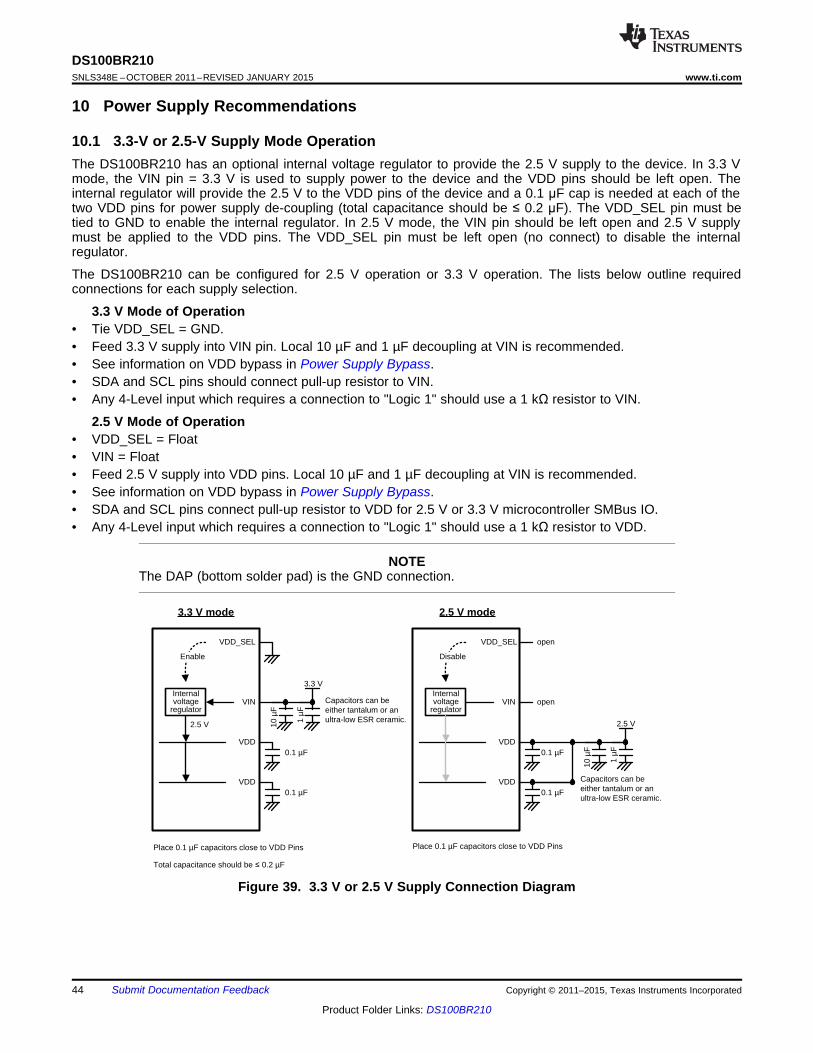
VDD_SEL
VIN
VDD
VDD
3.3 V
0.1 µF
0.1 µF
Internal voltage
regulator
Enable
2.5 V
VDD_SEL
VIN
VDD
VDD
Internal voltage
regulator
Disable
Place 0.1 µF capacitors close to VDD Pins
Total capacitance should be 7 0.2 µF
1 µ
F
10 µ
F
2.5 V
1 µ
F
10 µ
F0.1 µF
0.1 µF
Place 0.1 µF capacitors close to VDD Pins
open
openCapacitors can be either tantalum or an ultra-low ESR ceramic.
3.3 V mode 2.5 V mode
Capacitors can be either tantalum or an ultra-low ESR ceramic.
DS100BR210SNLS348E –OCTOBER 2011–REVISED JANUARY 2015 www.ti.com
10 Power Supply Recommendations
10.1 3.3-V or 2.5-V Supply Mode OperationThe DS100BR210 has an optional internal voltage regulator to provide the 2.5 V supply to the device. In 3.3 Vmode, the VIN pin = 3.3 V is used to supply power to the device and the VDD pins should be left open. Theinternal regulator will provide the 2.5 V to the VDD pins of the device and a 0.1 μF cap is needed at each of thetwo VDD pins for power supply de-coupling (total capacitance should be ≤ 0.2 μF). The VDD_SEL pin must betied to GND to enable the internal regulator. In 2.5 V mode, the VIN pin should be left open and 2.5 V supplymust be applied to the VDD pins. The VDD_SEL pin must be left open (no connect) to disable the internalregulator.
The DS100BR210 can be configured for 2.5 V operation or 3.3 V operation. The lists below outline requiredconnections for each supply selection.
3.3 V Mode of Operation• Tie VDD_SEL = GND.• Feed 3.3 V supply into VIN pin. Local 10 µF and 1 µF decoupling at VIN is recommended.• See information on VDD bypass in Power Supply Bypass.• SDA and SCL pins should connect pull-up resistor to VIN.• Any 4-Level input which requires a connection to "Logic 1" should use a 1 kΩ resistor to VIN.
2.5 V Mode of Operation• VDD_SEL = Float• VIN = Float• Feed 2.5 V supply into VDD pins. Local 10 µF and 1 µF decoupling at VIN is recommended.• See information on VDD bypass in Power Supply Bypass.• SDA and SCL pins connect pull-up resistor to VDD for 2.5 V or 3.3 V microcontroller SMBus IO.• Any 4-Level input which requires a connection to "Logic 1" should use a 1 kΩ resistor to VDD.
NOTEThe DAP (bottom solder pad) is the GND connection.
Figure 39. 3.3 V or 2.5 V Supply Connection Diagram
44 Submit Documentation Feedback Copyright © 2011–2015, Texas Instruments Incorporated
Product Folder Links: DS100BR210

DS100BR210www.ti.com SNLS348E –OCTOBER 2011–REVISED JANUARY 2015
10.2 Power Supply BypassTwo approaches are recommended to ensure that the DS100BR210 is provided with an adequate power supplybypass. First, the supply (VDD) and ground (GND) pins should be connected to power planes routed on adjacentlayers of the printed circuit board. Second, careful attention to supply bypassing through the proper use ofbypass capacitors is required. A 0.1 μF bypass capacitor should be connected to each VDD pin such that thecapacitor is placed as close as possible to the device. Small body size capacitors (such as 0402) reduce thecapacitors' parasitic inductance and also help in placement close to the VDD pin. If possible, the layer thicknessof the dielectric should be minimized so that the VDD and GND planes create a low inductance supply withdistributed capacitance.
11 Layout
11.1 Layout GuidelinesThe differential inputs and outputs are designed with 100 Ω differential terminations. Therefore, they should beconnected to interconnects with controlled differential impedance of approximately 85-110 Ω. It is preferable toroute differential lines primarily on one layer of the board, particularly for the input traces. The use of vias shouldbe avoided if possible. If vias must be used, they should be used sparingly and must be placed symmetrically foreach side of a given differential pair. Whenever differential vias are used, the layout must also provide for a lowinductance path for the return currents as well. Route the differential signals away from other signals and noisesources on the printed circuit board. To minimize the effects of crosstalk, a 5:1 ratio or greater should bemaintained between inter-pair spacing and trace width. See AN-1187 “Leadless Leadframe Package (LLP)Application Report” (literature number SNOA401) for additional information on QFN (WQFN) packages.
The DS100BR210 pinout promotes easy high speed routing and layout. To optimize DS100BR210 performance,refer to the following guidelines:1. Place local VIN and VDD capacitors as close as possible to the device supply pins. Often the best location is
directly under the DS100BR210 pins to reduce the inductance path to the capacitor. In addition, bypasscapacitors may share a via with the DAP GND to minimize ground loop inductance.
2. Differential pairs going into or out of the DS100BR210 should have adequate pair-to-pair spacing to minimizecrosstalk.
3. Use return current via connections to link reference planes locally. This ensures a low inductance returncurrent path when the differential signal changes layers.
4. Optimize the via structure to minimize trace impedance mismatch.5. Place GND vias around the DAP perimeter to ensure optimal electrical and thermal performance. A 2x2 or
3x3 array of GND vias for the DAP is recommended.6. Use small body size AC coupling capacitors when possible — 0402 or smaller size is preferred. The AC
coupling capacitors should be placed closer to the Rx on the channel.
11.2 Layout ExampleIn most cases, DS100BR210 layouts will fit neatly into a 2-channel application. The example layout in Figure 40shows the DS100BR210 channels in a typical 2-channel unidirectional layout.
Copyright © 2011–2015, Texas Instruments Incorporated Submit Documentation Feedback 45
Product Folder Links: DS100BR210
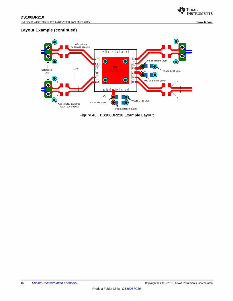
VDD
123456
22
21
20
19
24
23
9
10
11
12
GNDBOTTOM OF PKG
(TOP LAYER)
8
7
181716151413
1 2
1 2
12
12
12
12
VIN
55
5
7
7
55
5
7
7
> 25Via to GND Layer
Via to GND LayerVia to VIN Layer
Via to Bottom Layer
Pad on Bottom Layer
Pad on Bottom Layer
Via to GND Layer for return current path
Uniform trace width and spacing
DifferentialVias
DS100BR210SNLS348E –OCTOBER 2011–REVISED JANUARY 2015 www.ti.com
Layout Example (continued)
Figure 40. DS100BR210 Example Layout
46 Submit Documentation Feedback Copyright © 2011–2015, Texas Instruments Incorporated
Product Folder Links: DS100BR210

DS100BR210www.ti.com SNLS348E –OCTOBER 2011–REVISED JANUARY 2015
12 Device and Documentation Support
12.1 Documentation Support
12.1.1 Related DocumentationFor related documentation see the following:• Absolute Maximum Ratings for Soldering, SNOA549• IC Package Thermal Metrics application report, SPRA953• EEPROM Programming and Master Mode, SNLA228
12.2 TrademarksAll trademarks are the property of their respective owners.
12.3 Electrostatic Discharge CautionThese devices have limited built-in ESD protection. The leads should be shorted together or the device placed in conductive foamduring storage or handling to prevent electrostatic damage to the MOS gates.
12.4 GlossarySLYZ022 — TI Glossary.
This glossary lists and explains terms, acronyms, and definitions.
13 Mechanical, Packaging, and Orderable InformationThe following pages include mechanical, packaging, and orderable information. This information is the mostcurrent data available for the designated devices. This data is subject to change without notice and revision ofthis document. For browser-based versions of this data sheet, refer to the left-hand navigation.
Copyright © 2011–2015, Texas Instruments Incorporated Submit Documentation Feedback 47
Product Folder Links: DS100BR210

PACKAGE OPTION ADDENDUM
www.ti.com 10-Dec-2020
Addendum-Page 1
PACKAGING INFORMATION
Orderable Device Status(1)
Package Type PackageDrawing
Pins PackageQty
Eco Plan(2)
Lead finish/Ball material
(6)
MSL Peak Temp(3)
Op Temp (°C) Device Marking(4/5)
Samples
DS100BR210SQ/NOPB ACTIVE WQFN RTW 24 1000 RoHS & Green SN Level-3-260C-168 HR -40 to 85 BR210
DS100BR210SQE/NOPB ACTIVE WQFN RTW 24 250 RoHS & Green SN Level-3-260C-168 HR -40 to 85 BR210
(1) The marketing status values are defined as follows:ACTIVE: Product device recommended for new designs.LIFEBUY: TI has announced that the device will be discontinued, and a lifetime-buy period is in effect.NRND: Not recommended for new designs. Device is in production to support existing customers, but TI does not recommend using this part in a new design.PREVIEW: Device has been announced but is not in production. Samples may or may not be available.OBSOLETE: TI has discontinued the production of the device.
(2) RoHS: TI defines "RoHS" to mean semiconductor products that are compliant with the current EU RoHS requirements for all 10 RoHS substances, including the requirement that RoHS substancedo not exceed 0.1% by weight in homogeneous materials. Where designed to be soldered at high temperatures, "RoHS" products are suitable for use in specified lead-free processes. TI mayreference these types of products as "Pb-Free".RoHS Exempt: TI defines "RoHS Exempt" to mean products that contain lead but are compliant with EU RoHS pursuant to a specific EU RoHS exemption.Green: TI defines "Green" to mean the content of Chlorine (Cl) and Bromine (Br) based flame retardants meet JS709B low halogen requirements of <=1000ppm threshold. Antimony trioxide basedflame retardants must also meet the <=1000ppm threshold requirement.
(3) MSL, Peak Temp. - The Moisture Sensitivity Level rating according to the JEDEC industry standard classifications, and peak solder temperature.
(4) There may be additional marking, which relates to the logo, the lot trace code information, or the environmental category on the device.
(5) Multiple Device Markings will be inside parentheses. Only one Device Marking contained in parentheses and separated by a "~" will appear on a device. If a line is indented then it is a continuationof the previous line and the two combined represent the entire Device Marking for that device.
(6) Lead finish/Ball material - Orderable Devices may have multiple material finish options. Finish options are separated by a vertical ruled line. Lead finish/Ball material values may wrap to twolines if the finish value exceeds the maximum column width.
Important Information and Disclaimer:The information provided on this page represents TI's knowledge and belief as of the date that it is provided. TI bases its knowledge and belief on informationprovided by third parties, and makes no representation or warranty as to the accuracy of such information. Efforts are underway to better integrate information from third parties. TI has taken andcontinues to take reasonable steps to provide representative and accurate information but may not have conducted destructive testing or chemical analysis on incoming materials and chemicals.TI and TI suppliers consider certain information to be proprietary, and thus CAS numbers and other limited information may not be available for release.
In no event shall TI's liability arising out of such information exceed the total purchase price of the TI part(s) at issue in this document sold by TI to Customer on an annual basis.

PACKAGE OPTION ADDENDUM
www.ti.com 10-Dec-2020
Addendum-Page 2
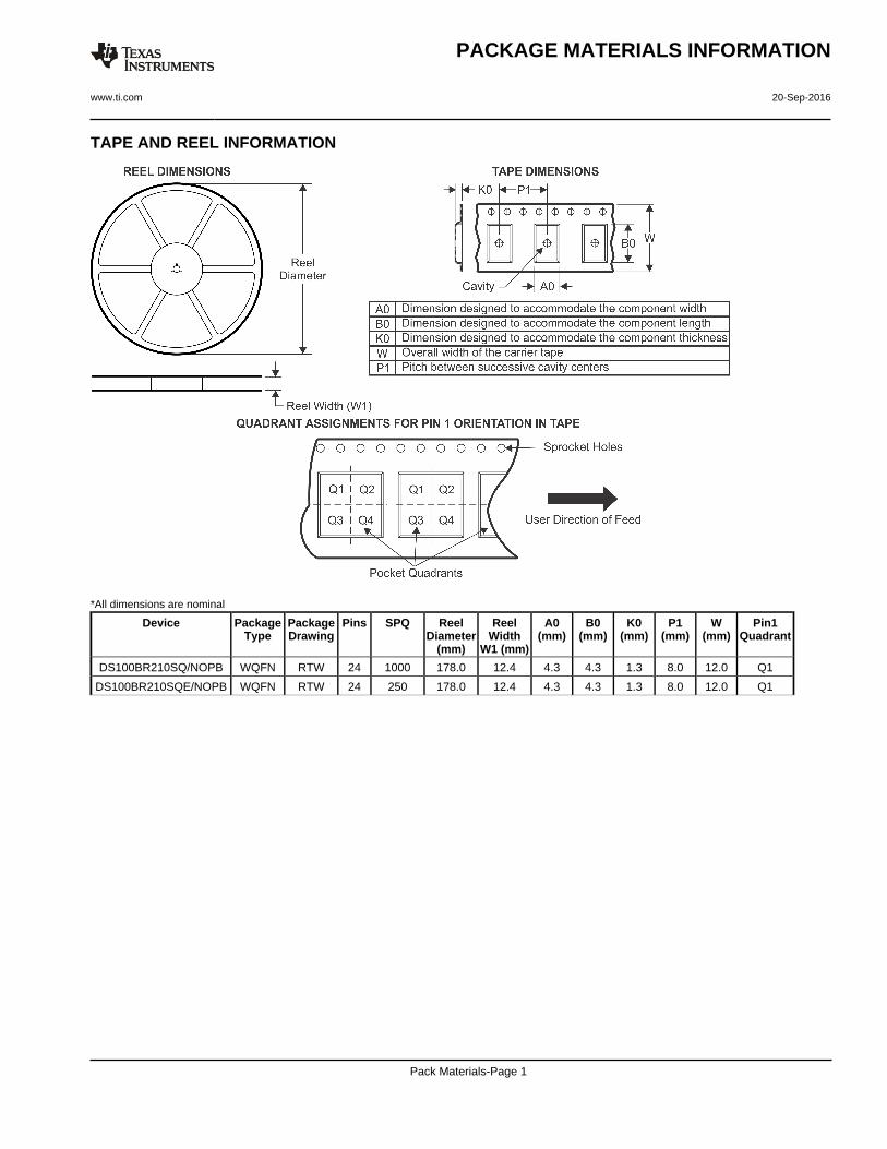
TAPE AND REEL INFORMATION
*All dimensions are nominal
Device PackageType
PackageDrawing
Pins SPQ ReelDiameter
(mm)
ReelWidth
W1 (mm)
A0(mm)
B0(mm)
K0(mm)
P1(mm)
W(mm)
Pin1Quadrant
DS100BR210SQ/NOPB WQFN RTW 24 1000 178.0 12.4 4.3 4.3 1.3 8.0 12.0 Q1
DS100BR210SQE/NOPB WQFN RTW 24 250 178.0 12.4 4.3 4.3 1.3 8.0 12.0 Q1
PACKAGE MATERIALS INFORMATION
www.ti.com 20-Sep-2016
Pack Materials-Page 1

*All dimensions are nominal
Device Package Type Package Drawing Pins SPQ Length (mm) Width (mm) Height (mm)
DS100BR210SQ/NOPB WQFN RTW 24 1000 210.0 185.0 35.0
DS100BR210SQE/NOPB WQFN RTW 24 250 210.0 185.0 35.0
PACKAGE MATERIALS INFORMATION
www.ti.com 20-Sep-2016
Pack Materials-Page 2

www.ti.com
PACKAGE OUTLINE
C
24X 0.30.2
24X 0.50.3
0.8 MAX
(0.1) TYP
0.050.00
20X 0.5
2X2.5
2X 2.5
2.6 0.1
A 4.13.9
B
4.13.9
WQFN - 0.8 mm max heightRTW0024APLASTIC QUAD FLATPACK - NO LEAD
4222815/A 03/2016
PIN 1 INDEX AREA
0.08 C
SEATING PLANE
1
6 13
18
7 12
24 19(OPTIONAL)
PIN 1 ID 0.1 C A B0.05 C
EXPOSEDTHERMAL PAD
25
NOTES: 1. All linear dimensions are in millimeters. Any dimensions in parenthesis are for reference only. Dimensioning and tolerancing per ASME Y14.5M. 2. This drawing is subject to change without notice. 3. The package thermal pad must be soldered to the printed circuit board for thermal and mechanical performance.
SCALE 3.000

www.ti.com
EXAMPLE BOARD LAYOUT
0.07 MINALL AROUND
0.07 MAXALL AROUND
24X (0.25)
24X (0.6)
( ) TYPVIA
0.2
20X (0.5)(3.8)
(3.8)
(1.05)
( 2.6)
(R )TYP
0.05
(1.05)
WQFN - 0.8 mm max heightRTW0024APLASTIC QUAD FLATPACK - NO LEAD
4222815/A 03/2016
SYMM
1
6
7 12
13
18
1924
SYMM
LAND PATTERN EXAMPLESCALE:15X
25
NOTES: (continued) 4. This package is designed to be soldered to a thermal pad on the board. For more information, see Texas Instruments literature number SLUA271 (www.ti.com/lit/slua271).
SOLDER MASKOPENING
METAL UNDERSOLDER MASK
SOLDER MASKDEFINED
METAL
SOLDER MASKOPENING
SOLDER MASK DETAILS
NON SOLDER MASKDEFINED
(PREFERRED)

www.ti.com
EXAMPLE STENCIL DESIGN
24X (0.6)
24X (0.25)
20X (0.5)
(3.8)
(3.8)
4X ( 1.15)
(0.675)TYP
(0.675) TYP(R ) TYP0.05
WQFN - 0.8 mm max heightRTW0024APLASTIC QUAD FLATPACK - NO LEAD
4222815/A 03/2016
NOTES: (continued) 5. Laser cutting apertures with trapezoidal walls and rounded corners may offer better paste release. IPC-7525 may have alternate design recommendations.
SYMM
METALTYP
SOLDER PASTE EXAMPLEBASED ON 0.125 mm THICK STENCIL
EXPOSED PAD 25:
78% PRINTED SOLDER COVERAGE BY AREA UNDER PACKAGESCALE:20X
SYMM
1
6
7 12
13
18
1924
25

IMPORTANT NOTICE AND DISCLAIMER
TI PROVIDES TECHNICAL AND RELIABILITY DATA (INCLUDING DATASHEETS), DESIGN RESOURCES (INCLUDING REFERENCE DESIGNS), APPLICATION OR OTHER DESIGN ADVICE, WEB TOOLS, SAFETY INFORMATION, AND OTHER RESOURCES “AS IS” AND WITH ALL FAULTS, AND DISCLAIMS ALL WARRANTIES, EXPRESS AND IMPLIED, INCLUDING WITHOUT LIMITATION ANY IMPLIED WARRANTIES OF MERCHANTABILITY, FITNESS FOR A PARTICULAR PURPOSE OR NON-INFRINGEMENT OF THIRD PARTY INTELLECTUAL PROPERTY RIGHTS.These resources are intended for skilled developers designing with TI products. You are solely responsible for (1) selecting the appropriate TI products for your application, (2) designing, validating and testing your application, and (3) ensuring your application meets applicable standards, and any other safety, security, or other requirements. These resources are subject to change without notice. TI grants you permission to use these resources only for development of an application that uses the TI products described in the resource. Other reproduction and display of these resources is prohibited. No license is granted to any other TI intellectual property right or to any third party intellectual property right. TI disclaims responsibility for, and you will fully indemnify TI and its representatives against, any claims, damages, costs, losses, and liabilities arising out of your use of these resources.TI’s products are provided subject to TI’s Terms of Sale (www.ti.com/legal/termsofsale.html) or other applicable terms available either on ti.com or provided in conjunction with such TI products. TI’s provision of these resources does not expand or otherwise alter TI’s applicable warranties or warranty disclaimers for TI products.
Mailing Address: Texas Instruments, Post Office Box 655303, Dallas, Texas 75265Copyright © 2020, Texas Instruments Incorporated