ds stm32f07x - home - stmicroelectronics docid025451 rev 6 contents 1 introduction . . . . . . . . ....
TRANSCRIPT

This is information on a product in full production.
January 2017 DocID025451 Rev 6 1/122
STM32F071x8 STM32F071xB
ARM®-based 32-bit MCU, up to 128 KB Flash, 12 timers, ADC, DAC and communication interfaces, 2.0 - 3.6 V
Datasheet - production data
Features
• Core: ARM® 32-bit Cortex®-M0 CPU, frequency up to 48 MHz
• Memories
– 64 to 128 Kbytes of Flash memory
– 16 Kbytes of SRAM with HW parity
• CRC calculation unit
• Reset and power management
– Digital and I/O supply: VDD = 2.0 V to 3.6 V
– Analog supply: VDDA = VDD to 3.6 V
– Selected I/Os: VDDIO2 = 1.65 V to 3.6 V
– Power-on/Power down reset (POR/PDR)
– Programmable voltage detector (PVD)
– Low power modes: Sleep, Stop, Standby
– VBAT supply for RTC and backup registers
• Clock management
– 4 to 32 MHz crystal oscillator
– 32 kHz oscillator for RTC with calibration
– Internal 8 MHz RC with x6 PLL option
– Internal 40 kHz RC oscillator
– Internal 48 MHz oscillator with automatic trimming based on ext. synchronization
• Up to 87 fast I/Os
– All mappable on external interrupt vectors
– Up to 68 I/Os with 5V tolerant capability and 19 with independent supply VDDIO2
• Seven-channel DMA controller
• One 12-bit, 1.0 µs ADC (up to 16 channels)
– Conversion range: 0 to 3.6 V
– Separate analog supply: 2.4 V to 3.6 V
• One 12-bit D/A converter (with 2 channels)
• Two fast low-power analog comparators with programmable input and output
• Up to 24 capacitive sensing channels for touchkey, linear and rotary touch sensors
• Calendar RTC with alarm and periodic wakeup from Stop/Standby
• 12 timers
– One 16-bit advanced-control timer for six-channel PWM output
– One 32-bit and seven 16-bit timers, with up to four IC/OC, OCN, usable for IR control decoding or DAC control
– Independent and system watchdog timers
– SysTick timer
• Communication interfaces
– Two I2C interfaces supporting Fast Mode Plus (1 Mbit/s) with 20 mA current sink, one supporting SMBus/PMBus and wakeup
– Four USARTs supporting master synchronous SPI and modem control, two with ISO7816 interface, LIN, IrDA, auto baud rate detection and wakeup feature
– Two SPIs (18 Mbit/s) with 4 to 16 programmable bit frames, and with I2S interface multiplexed
• HDMI CEC, wakeup on header reception
• Serial wire debug (SWD)
• 96-bit unique ID
• All packages ECOPACK®2
Table 1. Device summary
Reference Part number
STM32F071x8 STM32F071xB
STM32F071C8, STM32F071V8 STM32F071CB, STM32F071RB, STM32F071VB
LQFP100 14x14 mmLQFP64 10x10 mm
LQFP48 7x7 mm
UFQFPN487x7 mm
UFBGA1007x7 mm
WLCSP493.3x3.1 mm
www.st.com

Contents STM32F071x8 STM32F071xB
2/122 DocID025451 Rev 6
Contents
1 Introduction . . . . . . . . . . . . . . . . . . . . . . . . . . . . . . . . . . . . . . . . . . . . . . . . 9
2 Description . . . . . . . . . . . . . . . . . . . . . . . . . . . . . . . . . . . . . . . . . . . . . . . . 10
3 Functional overview . . . . . . . . . . . . . . . . . . . . . . . . . . . . . . . . . . . . . . . . 13
3.1 ARM®-Cortex®-M0 core . . . . . . . . . . . . . . . . . . . . . . . . . . . . . . . . . . . . . . 13
3.2 Memories . . . . . . . . . . . . . . . . . . . . . . . . . . . . . . . . . . . . . . . . . . . . . . . . . 13
3.3 Boot modes . . . . . . . . . . . . . . . . . . . . . . . . . . . . . . . . . . . . . . . . . . . . . . . 13
3.4 Cyclic redundancy check calculation unit (CRC) . . . . . . . . . . . . . . . . . . . 14
3.5 Power management . . . . . . . . . . . . . . . . . . . . . . . . . . . . . . . . . . . . . . . . . 14
3.5.1 Power supply schemes . . . . . . . . . . . . . . . . . . . . . . . . . . . . . . . . . . . . . 14
3.5.2 Power supply supervisors . . . . . . . . . . . . . . . . . . . . . . . . . . . . . . . . . . . 14
3.5.3 Voltage regulator . . . . . . . . . . . . . . . . . . . . . . . . . . . . . . . . . . . . . . . . . . 15
3.5.4 Low-power modes . . . . . . . . . . . . . . . . . . . . . . . . . . . . . . . . . . . . . . . . . 15
3.6 Clocks and startup . . . . . . . . . . . . . . . . . . . . . . . . . . . . . . . . . . . . . . . . . . 15
3.7 General-purpose inputs/outputs (GPIOs) . . . . . . . . . . . . . . . . . . . . . . . . . 17
3.8 Direct memory access controller (DMA) . . . . . . . . . . . . . . . . . . . . . . . . . . 17
3.9 Interrupts and events . . . . . . . . . . . . . . . . . . . . . . . . . . . . . . . . . . . . . . . . 17
3.9.1 Nested vectored interrupt controller (NVIC) . . . . . . . . . . . . . . . . . . . . . . 17
3.9.2 Extended interrupt/event controller (EXTI) . . . . . . . . . . . . . . . . . . . . . . 18
3.10 Analog-to-digital converter (ADC) . . . . . . . . . . . . . . . . . . . . . . . . . . . . . . 18
3.10.1 Temperature sensor . . . . . . . . . . . . . . . . . . . . . . . . . . . . . . . . . . . . . . . . 18
3.10.2 Internal voltage reference (VREFINT) . . . . . . . . . . . . . . . . . . . . . . . . . . . 18
3.10.3 VBAT battery voltage monitoring . . . . . . . . . . . . . . . . . . . . . . . . . . . . . . . 19
3.11 Digital-to-analog converter (DAC) . . . . . . . . . . . . . . . . . . . . . . . . . . . . . . 19
3.12 Comparators (COMP) . . . . . . . . . . . . . . . . . . . . . . . . . . . . . . . . . . . . . . . 19
3.13 Touch sensing controller (TSC) . . . . . . . . . . . . . . . . . . . . . . . . . . . . . . . . 20
3.14 Timers and watchdogs . . . . . . . . . . . . . . . . . . . . . . . . . . . . . . . . . . . . . . . 21
3.14.1 Advanced-control timer (TIM1) . . . . . . . . . . . . . . . . . . . . . . . . . . . . . . . 22
3.14.2 General-purpose timers (TIM2, 3, 14, 15, 16, 17) . . . . . . . . . . . . . . . . . 22
3.14.3 Basic timers TIM6 and TIM7 . . . . . . . . . . . . . . . . . . . . . . . . . . . . . . . . . 23
3.14.4 Independent watchdog (IWDG) . . . . . . . . . . . . . . . . . . . . . . . . . . . . . . . 23
3.14.5 System window watchdog (WWDG) . . . . . . . . . . . . . . . . . . . . . . . . . . . 23

DocID025451 Rev 6 3/122
STM32F071x8 STM32F071xB Contents
4
3.14.6 SysTick timer . . . . . . . . . . . . . . . . . . . . . . . . . . . . . . . . . . . . . . . . . . . . . 23
3.15 Real-time clock (RTC) and backup registers . . . . . . . . . . . . . . . . . . . . . . 23
3.16 Inter-integrated circuit interface (I2C) . . . . . . . . . . . . . . . . . . . . . . . . . . . . 24
3.17 Universal synchronous/asynchronous receiver/transmitter (USART) . . . 25
3.18 Serial peripheral interface (SPI) / Inter-integrated sound interface (I2S) . 26
3.19 High-definition multimedia interface (HDMI) - consumer electronics control (CEC) . . . . . . . . . . . . . . . . . . . . . . . . . . . . . . . . . . . . . 26
3.20 Clock recovery system (CRS) . . . . . . . . . . . . . . . . . . . . . . . . . . . . . . . . . 27
3.21 Serial wire debug port (SW-DP) . . . . . . . . . . . . . . . . . . . . . . . . . . . . . . . . 27
4 Pinouts and pin descriptions . . . . . . . . . . . . . . . . . . . . . . . . . . . . . . . . . 28
5 Memory mapping . . . . . . . . . . . . . . . . . . . . . . . . . . . . . . . . . . . . . . . . . . . 43
6 Electrical characteristics . . . . . . . . . . . . . . . . . . . . . . . . . . . . . . . . . . . . 46
6.1 Parameter conditions . . . . . . . . . . . . . . . . . . . . . . . . . . . . . . . . . . . . . . . . 46
6.1.1 Minimum and maximum values . . . . . . . . . . . . . . . . . . . . . . . . . . . . . . . 46
6.1.2 Typical values . . . . . . . . . . . . . . . . . . . . . . . . . . . . . . . . . . . . . . . . . . . . 46
6.1.3 Typical curves . . . . . . . . . . . . . . . . . . . . . . . . . . . . . . . . . . . . . . . . . . . . 46
6.1.4 Loading capacitor . . . . . . . . . . . . . . . . . . . . . . . . . . . . . . . . . . . . . . . . . 46
6.1.5 Pin input voltage . . . . . . . . . . . . . . . . . . . . . . . . . . . . . . . . . . . . . . . . . . 46
6.1.6 Power supply scheme . . . . . . . . . . . . . . . . . . . . . . . . . . . . . . . . . . . . . . 47
6.1.7 Current consumption measurement . . . . . . . . . . . . . . . . . . . . . . . . . . . 48
6.2 Absolute maximum ratings . . . . . . . . . . . . . . . . . . . . . . . . . . . . . . . . . . . . 49
6.3 Operating conditions . . . . . . . . . . . . . . . . . . . . . . . . . . . . . . . . . . . . . . . . 51
6.3.1 General operating conditions . . . . . . . . . . . . . . . . . . . . . . . . . . . . . . . . . 51
6.3.2 Operating conditions at power-up / power-down . . . . . . . . . . . . . . . . . . 51
6.3.3 Embedded reset and power control block characteristics . . . . . . . . . . . 52
6.3.4 Embedded reference voltage . . . . . . . . . . . . . . . . . . . . . . . . . . . . . . . . . 53
6.3.5 Supply current characteristics . . . . . . . . . . . . . . . . . . . . . . . . . . . . . . . . 53
6.3.6 Wakeup time from low-power mode . . . . . . . . . . . . . . . . . . . . . . . . . . . 64
6.3.7 External clock source characteristics . . . . . . . . . . . . . . . . . . . . . . . . . . . 64
6.3.8 Internal clock source characteristics . . . . . . . . . . . . . . . . . . . . . . . . . . . 68
6.3.9 PLL characteristics . . . . . . . . . . . . . . . . . . . . . . . . . . . . . . . . . . . . . . . . 72
6.3.10 Memory characteristics . . . . . . . . . . . . . . . . . . . . . . . . . . . . . . . . . . . . . 72
6.3.11 EMC characteristics . . . . . . . . . . . . . . . . . . . . . . . . . . . . . . . . . . . . . . . . 73
Contents STM32F071x8 STM32F071xB
4/122 DocID025451 Rev 6
6.3.12 Electrical sensitivity characteristics . . . . . . . . . . . . . . . . . . . . . . . . . . . . 74
6.3.13 I/O current injection characteristics . . . . . . . . . . . . . . . . . . . . . . . . . . . . 75
6.3.14 I/O port characteristics . . . . . . . . . . . . . . . . . . . . . . . . . . . . . . . . . . . . . . 76
6.3.15 NRST pin characteristics . . . . . . . . . . . . . . . . . . . . . . . . . . . . . . . . . . . . 81
6.3.16 12-bit ADC characteristics . . . . . . . . . . . . . . . . . . . . . . . . . . . . . . . . . . . 82
6.3.17 DAC electrical specifications . . . . . . . . . . . . . . . . . . . . . . . . . . . . . . . . . 86
6.3.18 Comparator characteristics . . . . . . . . . . . . . . . . . . . . . . . . . . . . . . . . . . 88
6.3.19 Temperature sensor characteristics . . . . . . . . . . . . . . . . . . . . . . . . . . . . 90
6.3.20 VBAT monitoring characteristics . . . . . . . . . . . . . . . . . . . . . . . . . . . . . . . 90
6.3.21 Timer characteristics . . . . . . . . . . . . . . . . . . . . . . . . . . . . . . . . . . . . . . . 90
6.3.22 Communication interfaces . . . . . . . . . . . . . . . . . . . . . . . . . . . . . . . . . . . 91
7 Package information . . . . . . . . . . . . . . . . . . . . . . . . . . . . . . . . . . . . . . . . 97
7.1 UFBGA100 package information . . . . . . . . . . . . . . . . . . . . . . . . . . . . . . . 97
7.2 LQFP100 package information . . . . . . . . . . . . . . . . . . . . . . . . . . . . . . . . 100
7.3 LQFP64 package information . . . . . . . . . . . . . . . . . . . . . . . . . . . . . . . . 103
7.4 WLCSP49 package information . . . . . . . . . . . . . . . . . . . . . . . . . . . . . . . 106
7.5 LQFP48 package information . . . . . . . . . . . . . . . . . . . . . . . . . . . . . . . . . 109
7.6 UFQFPN48 package information . . . . . . . . . . . . . . . . . . . . . . . . . . . . . . .112
7.7 Thermal characteristics . . . . . . . . . . . . . . . . . . . . . . . . . . . . . . . . . . . . . .115
7.7.1 Reference document . . . . . . . . . . . . . . . . . . . . . . . . . . . . . . . . . . . . . . 115
7.7.2 Selecting the product temperature range . . . . . . . . . . . . . . . . . . . . . . 115
8 Ordering information . . . . . . . . . . . . . . . . . . . . . . . . . . . . . . . . . . . . . . 118
9 Revision history . . . . . . . . . . . . . . . . . . . . . . . . . . . . . . . . . . . . . . . . . . 119

DocID025451 Rev 6 5/122
STM32F071x8 STM32F071xB List of tables
6
List of tables
Table 1. Device summary . . . . . . . . . . . . . . . . . . . . . . . . . . . . . . . . . . . . . . . . . . . . . . . . . . . . . . . . . . 1Table 2. STM32F071x8/xB family device features and peripheral counts . . . . . . . . . . . . . . . . . . . . 11Table 3. Temperature sensor calibration values. . . . . . . . . . . . . . . . . . . . . . . . . . . . . . . . . . . . . . . . 18Table 4. Internal voltage reference calibration values . . . . . . . . . . . . . . . . . . . . . . . . . . . . . . . . . . . 19Table 5. Capacitive sensing GPIOs available on STM32F071x8/xB devices. . . . . . . . . . . . . . . . . . 20Table 6. Number of capacitive sensing channels available
on STM32F071x8/xB devices . . . . . . . . . . . . . . . . . . . . . . . . . . . . . . . . . . . . . . . . . . . . . . 21Table 7. Timer feature comparison. . . . . . . . . . . . . . . . . . . . . . . . . . . . . . . . . . . . . . . . . . . . . . . . . . 21Table 8. Comparison of I2C analog and digital filters . . . . . . . . . . . . . . . . . . . . . . . . . . . . . . . . . . . . 24Table 9. STM32F071x8/xB I2C implementation . . . . . . . . . . . . . . . . . . . . . . . . . . . . . . . . . . . . . . . . 25Table 10. STM32F071x8/xB USART implementation . . . . . . . . . . . . . . . . . . . . . . . . . . . . . . . . . . . . 25Table 11. STM32F071x8/xB SPI/I2S implementation. . . . . . . . . . . . . . . . . . . . . . . . . . . . . . . . . . . . . 26Table 12. Legend/abbreviations used in the pinout table . . . . . . . . . . . . . . . . . . . . . . . . . . . . . . . . . . 32Table 13. STM32F071x8/xB pin definitions . . . . . . . . . . . . . . . . . . . . . . . . . . . . . . . . . . . . . . . . . . . . 32Table 14. Alternate functions selected through GPIOA_AFR registers for port A . . . . . . . . . . . . . . . 39Table 15. Alternate functions selected through GPIOB_AFR registers for port B . . . . . . . . . . . . . . . 40Table 16. Alternate functions selected through GPIOC_AFR registers for port C . . . . . . . . . . . . . . . 41Table 17. Alternate functions selected through GPIOD_AFR registers for port D . . . . . . . . . . . . . . . 41Table 18. Alternate functions selected through GPIOE_AFR registers for port E . . . . . . . . . . . . . . . 42Table 19. Alternate functions available on port F . . . . . . . . . . . . . . . . . . . . . . . . . . . . . . . . . . . . . . . . 42Table 20. STM32F071x8/xB peripheral register boundary addresses . . . . . . . . . . . . . . . . . . . . . . . . 44Table 21. Voltage characteristics . . . . . . . . . . . . . . . . . . . . . . . . . . . . . . . . . . . . . . . . . . . . . . . . . . . . 49Table 22. Current characteristics . . . . . . . . . . . . . . . . . . . . . . . . . . . . . . . . . . . . . . . . . . . . . . . . . . . . 50Table 23. Thermal characteristics. . . . . . . . . . . . . . . . . . . . . . . . . . . . . . . . . . . . . . . . . . . . . . . . . . . . 50Table 24. General operating conditions . . . . . . . . . . . . . . . . . . . . . . . . . . . . . . . . . . . . . . . . . . . . . . . 51Table 25. Operating conditions at power-up / power-down . . . . . . . . . . . . . . . . . . . . . . . . . . . . . . . . 52Table 26. Embedded reset and power control block characteristics. . . . . . . . . . . . . . . . . . . . . . . . . . 52Table 27. Programmable voltage detector characteristics . . . . . . . . . . . . . . . . . . . . . . . . . . . . . . . . . 52Table 28. Embedded internal reference voltage. . . . . . . . . . . . . . . . . . . . . . . . . . . . . . . . . . . . . . . . . 53Table 29. Typical and maximum current consumption from VDD supply at VDD = 3.6 V . . . . . . . . . . 54Table 30. Typical and maximum current consumption from the VDDA supply . . . . . . . . . . . . . . . . . 56Table 31. Typical and maximum consumption in Stop and Standby modes . . . . . . . . . . . . . . . . . . . 57Table 32. Typical and maximum current consumption from the VBAT supply. . . . . . . . . . . . . . . . . . . 58Table 33. Typical current consumption, code executing from Flash memory,
running from HSE 8 MHz crystal . . . . . . . . . . . . . . . . . . . . . . . . . . . . . . . . . . . . . . . . . . . . 59Table 34. Switching output I/O current consumption . . . . . . . . . . . . . . . . . . . . . . . . . . . . . . . . . . . . . 61Table 35. Peripheral current consumption . . . . . . . . . . . . . . . . . . . . . . . . . . . . . . . . . . . . . . . . . . . . . 62Table 36. Low-power mode wakeup timings . . . . . . . . . . . . . . . . . . . . . . . . . . . . . . . . . . . . . . . . . . . 64Table 37. High-speed external user clock characteristics. . . . . . . . . . . . . . . . . . . . . . . . . . . . . . . . . . 64Table 38. Low-speed external user clock characteristics . . . . . . . . . . . . . . . . . . . . . . . . . . . . . . . . . . 65Table 39. HSE oscillator characteristics . . . . . . . . . . . . . . . . . . . . . . . . . . . . . . . . . . . . . . . . . . . . . . . 66Table 40. LSE oscillator characteristics (fLSE = 32.768 kHz) . . . . . . . . . . . . . . . . . . . . . . . . . . . . . . . 67Table 41. HSI oscillator characteristics. . . . . . . . . . . . . . . . . . . . . . . . . . . . . . . . . . . . . . . . . . . . . . . . 69Table 42. HSI14 oscillator characteristics. . . . . . . . . . . . . . . . . . . . . . . . . . . . . . . . . . . . . . . . . . . . . . 70Table 43. HSI48 oscillator characteristics. . . . . . . . . . . . . . . . . . . . . . . . . . . . . . . . . . . . . . . . . . . . . . 71Table 44. LSI oscillator characteristics . . . . . . . . . . . . . . . . . . . . . . . . . . . . . . . . . . . . . . . . . . . . . . . . 72Table 45. PLL characteristics . . . . . . . . . . . . . . . . . . . . . . . . . . . . . . . . . . . . . . . . . . . . . . . . . . . . . . . 72Table 46. Flash memory characteristics . . . . . . . . . . . . . . . . . . . . . . . . . . . . . . . . . . . . . . . . . . . . . . . 72
List of tables STM32F071x8 STM32F071xB
6/122 DocID025451 Rev 6
Table 47. Flash memory endurance and data retention . . . . . . . . . . . . . . . . . . . . . . . . . . . . . . . . . . . 73Table 48. EMS characteristics . . . . . . . . . . . . . . . . . . . . . . . . . . . . . . . . . . . . . . . . . . . . . . . . . . . . . . 73Table 49. EMI characteristics . . . . . . . . . . . . . . . . . . . . . . . . . . . . . . . . . . . . . . . . . . . . . . . . . . . . . . . 74Table 50. ESD absolute maximum ratings . . . . . . . . . . . . . . . . . . . . . . . . . . . . . . . . . . . . . . . . . . . . . 75Table 51. Electrical sensitivities . . . . . . . . . . . . . . . . . . . . . . . . . . . . . . . . . . . . . . . . . . . . . . . . . . . . . 75Table 52. I/O current injection susceptibility . . . . . . . . . . . . . . . . . . . . . . . . . . . . . . . . . . . . . . . . . . . . 76Table 53. I/O static characteristics . . . . . . . . . . . . . . . . . . . . . . . . . . . . . . . . . . . . . . . . . . . . . . . . . . . 76Table 54. Output voltage characteristics . . . . . . . . . . . . . . . . . . . . . . . . . . . . . . . . . . . . . . . . . . . . . . 79Table 55. I/O AC characteristics . . . . . . . . . . . . . . . . . . . . . . . . . . . . . . . . . . . . . . . . . . . . . . . . . . . . . 80Table 56. NRST pin characteristics . . . . . . . . . . . . . . . . . . . . . . . . . . . . . . . . . . . . . . . . . . . . . . . . . . 81Table 57. ADC characteristics . . . . . . . . . . . . . . . . . . . . . . . . . . . . . . . . . . . . . . . . . . . . . . . . . . . . . . 82Table 58. RAIN max for fADC = 14 MHz. . . . . . . . . . . . . . . . . . . . . . . . . . . . . . . . . . . . . . . . . . . . . . . . 84Table 59. ADC accuracy. . . . . . . . . . . . . . . . . . . . . . . . . . . . . . . . . . . . . . . . . . . . . . . . . . . . . . . . . . . 84Table 60. DAC characteristics . . . . . . . . . . . . . . . . . . . . . . . . . . . . . . . . . . . . . . . . . . . . . . . . . . . . . . 86Table 61. Comparator characteristics. . . . . . . . . . . . . . . . . . . . . . . . . . . . . . . . . . . . . . . . . . . . . . . . . 88Table 62. TS characteristics . . . . . . . . . . . . . . . . . . . . . . . . . . . . . . . . . . . . . . . . . . . . . . . . . . . . . . . . 90Table 63. VBAT monitoring characteristics . . . . . . . . . . . . . . . . . . . . . . . . . . . . . . . . . . . . . . . . . . . . . 90Table 64. TIMx characteristics . . . . . . . . . . . . . . . . . . . . . . . . . . . . . . . . . . . . . . . . . . . . . . . . . . . . . . 90Table 65. IWDG min/max timeout period at 40 kHz (LSI). . . . . . . . . . . . . . . . . . . . . . . . . . . . . . . . . . 91Table 66. WWDG min/max timeout value at 48 MHz (PCLK). . . . . . . . . . . . . . . . . . . . . . . . . . . . . . . 91Table 67. I2C analog filter characteristics . . . . . . . . . . . . . . . . . . . . . . . . . . . . . . . . . . . . . . . . . . . . . . 92Table 68. SPI characteristics . . . . . . . . . . . . . . . . . . . . . . . . . . . . . . . . . . . . . . . . . . . . . . . . . . . . . . . 92Table 69. I2S characteristics. . . . . . . . . . . . . . . . . . . . . . . . . . . . . . . . . . . . . . . . . . . . . . . . . . . . . . . . 94Table 70. UFBGA100 package mechanical data . . . . . . . . . . . . . . . . . . . . . . . . . . . . . . . . . . . . . . . . 97Table 71. UFBGA100 recommended PCB design rules. . . . . . . . . . . . . . . . . . . . . . . . . . . . . . . . . . . 98Table 72. LQPF100 package mechanical data. . . . . . . . . . . . . . . . . . . . . . . . . . . . . . . . . . . . . . . . . 100Table 73. LQFP64 package mechanical data. . . . . . . . . . . . . . . . . . . . . . . . . . . . . . . . . . . . . . . . . . 103Table 74. WLCSP49 package mechanical data . . . . . . . . . . . . . . . . . . . . . . . . . . . . . . . . . . . . . . . . 107Table 75. LQFP48 package mechanical data. . . . . . . . . . . . . . . . . . . . . . . . . . . . . . . . . . . . . . . . . . 110Table 76. UFQFPN48 package mechanical data . . . . . . . . . . . . . . . . . . . . . . . . . . . . . . . . . . . . . . . 113Table 77. Package thermal characteristics . . . . . . . . . . . . . . . . . . . . . . . . . . . . . . . . . . . . . . . . . . . . 115Table 78. Ordering information scheme . . . . . . . . . . . . . . . . . . . . . . . . . . . . . . . . . . . . . . . . . . . . . . 118Table 79. Document revision history . . . . . . . . . . . . . . . . . . . . . . . . . . . . . . . . . . . . . . . . . . . . . . . . 119

DocID025451 Rev 6 7/122
STM32F071x8 STM32F071xB List of figures
8
List of figures
Figure 1. Block diagram . . . . . . . . . . . . . . . . . . . . . . . . . . . . . . . . . . . . . . . . . . . . . . . . . . . . . . . . . . . 12Figure 2. Clock tree . . . . . . . . . . . . . . . . . . . . . . . . . . . . . . . . . . . . . . . . . . . . . . . . . . . . . . . . . . . . . . 16Figure 3. UFBGA100 package pinout . . . . . . . . . . . . . . . . . . . . . . . . . . . . . . . . . . . . . . . . . . . . . . . . 28Figure 4. LQFP100 package pinout . . . . . . . . . . . . . . . . . . . . . . . . . . . . . . . . . . . . . . . . . . . . . . . . 29Figure 5. LQFP64 package pinout . . . . . . . . . . . . . . . . . . . . . . . . . . . . . . . . . . . . . . . . . . . . . . . . . . . 30Figure 6. LQFP48 package pinout . . . . . . . . . . . . . . . . . . . . . . . . . . . . . . . . . . . . . . . . . . . . . . . . . . . 30Figure 7. UFQFPN48 package pinout . . . . . . . . . . . . . . . . . . . . . . . . . . . . . . . . . . . . . . . . . . . . . . . . 31Figure 8. WLCSP49 package pinout . . . . . . . . . . . . . . . . . . . . . . . . . . . . . . . . . . . . . . . . . . . . . . . . . 31Figure 9. STM32F071xB memory map . . . . . . . . . . . . . . . . . . . . . . . . . . . . . . . . . . . . . . . . . . . . . 43Figure 10. Pin loading conditions. . . . . . . . . . . . . . . . . . . . . . . . . . . . . . . . . . . . . . . . . . . . . . . . . . . . . 46Figure 11. Pin input voltage . . . . . . . . . . . . . . . . . . . . . . . . . . . . . . . . . . . . . . . . . . . . . . . . . . . . . . . . . 46Figure 12. Power supply scheme . . . . . . . . . . . . . . . . . . . . . . . . . . . . . . . . . . . . . . . . . . . . . . . . . . . . 47Figure 13. Current consumption measurement scheme . . . . . . . . . . . . . . . . . . . . . . . . . . . . . . . . . . . 48Figure 14. High-speed external clock source AC timing diagram . . . . . . . . . . . . . . . . . . . . . . . . . . . . 65Figure 15. Low-speed external clock source AC timing diagram. . . . . . . . . . . . . . . . . . . . . . . . . . . . . 65Figure 16. Typical application with an 8 MHz crystal . . . . . . . . . . . . . . . . . . . . . . . . . . . . . . . . . . . . . . 67Figure 17. Typical application with a 32.768 kHz crystal . . . . . . . . . . . . . . . . . . . . . . . . . . . . . . . . . . . 68Figure 18. HSI oscillator accuracy characterization results for soldered parts . . . . . . . . . . . . . . . . . . 69Figure 19. HSI14 oscillator accuracy characterization results . . . . . . . . . . . . . . . . . . . . . . . . . . . . . . . 70Figure 20. HSI48 oscillator accuracy characterization results . . . . . . . . . . . . . . . . . . . . . . . . . . . . . . . 71Figure 21. TC and TTa I/O input characteristics . . . . . . . . . . . . . . . . . . . . . . . . . . . . . . . . . . . . . . . . . 78Figure 22. Five volt tolerant (FT and FTf) I/O input characteristics . . . . . . . . . . . . . . . . . . . . . . . . . . . 78Figure 23. I/O AC characteristics definition . . . . . . . . . . . . . . . . . . . . . . . . . . . . . . . . . . . . . . . . . . . . . 81Figure 24. Recommended NRST pin protection . . . . . . . . . . . . . . . . . . . . . . . . . . . . . . . . . . . . . . . . . 82Figure 25. ADC accuracy characteristics . . . . . . . . . . . . . . . . . . . . . . . . . . . . . . . . . . . . . . . . . . . . . . . 85Figure 26. Typical connection diagram using the ADC . . . . . . . . . . . . . . . . . . . . . . . . . . . . . . . . . . . . 85Figure 27. 12-bit buffered / non-buffered DAC. . . . . . . . . . . . . . . . . . . . . . . . . . . . . . . . . . . . . . . . . . . 87Figure 28. Maximum VREFINT scaler startup time from power down . . . . . . . . . . . . . . . . . . . . . . . . . . 89Figure 29. SPI timing diagram - slave mode and CPHA = 0 . . . . . . . . . . . . . . . . . . . . . . . . . . . . . . . . 93Figure 30. SPI timing diagram - slave mode and CPHA = 1 . . . . . . . . . . . . . . . . . . . . . . . . . . . . . . . . 93Figure 31. SPI timing diagram - master mode . . . . . . . . . . . . . . . . . . . . . . . . . . . . . . . . . . . . . . . . . . . 94Figure 32. I2S slave timing diagram (Philips protocol) . . . . . . . . . . . . . . . . . . . . . . . . . . . . . . . . . . . . . 95Figure 33. I2S master timing diagram (Philips protocol). . . . . . . . . . . . . . . . . . . . . . . . . . . . . . . . . . . . 96Figure 34. UFBGA100 package outline . . . . . . . . . . . . . . . . . . . . . . . . . . . . . . . . . . . . . . . . . . . . . . . . 97Figure 35. Recommended footprint for UFBGA100 package . . . . . . . . . . . . . . . . . . . . . . . . . . . . . . . 98Figure 36. UFBGA100 package marking example . . . . . . . . . . . . . . . . . . . . . . . . . . . . . . . . . . . . . . . 99Figure 37. LQFP100 package outline . . . . . . . . . . . . . . . . . . . . . . . . . . . . . . . . . . . . . . . . . . . . . . . . 100Figure 38. Recommended footprint for LQFP100 package . . . . . . . . . . . . . . . . . . . . . . . . . . . . . . . . 101Figure 39. LQFP100 package marking example . . . . . . . . . . . . . . . . . . . . . . . . . . . . . . . . . . . . . . . . 102Figure 40. LQFP64 package outline . . . . . . . . . . . . . . . . . . . . . . . . . . . . . . . . . . . . . . . . . . . . . . . . . 103Figure 41. Recommended footprint for LQFP64 package . . . . . . . . . . . . . . . . . . . . . . . . . . . . . . . . . 104Figure 42. LQFP64 package marking example . . . . . . . . . . . . . . . . . . . . . . . . . . . . . . . . . . . . . . . . . 105Figure 43. WLCSP49 package outline. . . . . . . . . . . . . . . . . . . . . . . . . . . . . . . . . . . . . . . . . . . . . . . . 106Figure 44. WLCSP49 package marking example . . . . . . . . . . . . . . . . . . . . . . . . . . . . . . . . . . . . . . . 108Figure 45. LQFP48 package outline . . . . . . . . . . . . . . . . . . . . . . . . . . . . . . . . . . . . . . . . . . . . . . . . . 109Figure 46. Recommended footprint for LQFP48 package . . . . . . . . . . . . . . . . . . . . . . . . . . . . . . . . . 110Figure 47. LQFP48 package marking example . . . . . . . . . . . . . . . . . . . . . . . . . . . . . . . . . . . . . . . . . 111Figure 48. UFQFPN48 package outline. . . . . . . . . . . . . . . . . . . . . . . . . . . . . . . . . . . . . . . . . . . . . . . 112

List of figures STM32F071x8 STM32F071xB
8/122 DocID025451 Rev 6
Figure 49. Recommended footprint for UFQFPN48 package . . . . . . . . . . . . . . . . . . . . . . . . . . . . . . 113Figure 50. UFQFPN48 package marking example . . . . . . . . . . . . . . . . . . . . . . . . . . . . . . . . . . . . . . 114Figure 51. LQFP64 PD max versus TA . . . . . . . . . . . . . . . . . . . . . . . . . . . . . . . . . . . . . . . . . . . . . . . 117

DocID025451 Rev 6 9/122
STM32F071x8 STM32F071xB Introduction
27
1 Introduction
This datasheet provides the ordering information and mechanical device characteristics of the STM32F071x8/xB microcontrollers.
This document should be read in conjunction with the STM32F0xxxx reference manual (RM0091). The reference manual is available from the STMicroelectronics website www.st.com.
For information on the ARM® Cortex®-M0 core, please refer to the Cortex®-M0 Technical Reference Manual, available from the www.arm.com website.
Description STM32F071x8 STM32F071xB
10/122 DocID025451 Rev 6
2 Description
The STM32F071x8/xB microcontrollers incorporate the high-performance ARM® Cortex®-M0 32-bit RISC core operating at up to 48 MHz frequency, high-speed embedded memories (up to 128 Kbytes of Flash memory and 16 Kbytes of SRAM), and an extensive range of enhanced peripherals and I/Os. All devices offer standard communication interfaces (two I2Cs, two SPI/one I2S, one HDMI CEC and four USARTs), one 12-bit ADC, one 12-bit DAC with two channels, seven 16-bit timers, one 32-bit timer and an advanced-control PWM timer.
The STM32F071x8/xB microcontrollers operate in the -40 to +85 °C and -40 to +105 °C temperature ranges, from a 2.0 to 3.6 V power supply. A comprehensive set of power-saving modes allows the design of low-power applications.
The STM32F071x8/xB microcontrollers include devices in six different packages ranging from 48 pins to 100 pins with a die form also available upon request. Depending on the device chosen, different sets of peripherals are included.
These features make the STM32F071x8/xB microcontrollers suitable for a wide range of applications such as application control and user interfaces, hand-held equipment, A/V receivers and digital TV, PC peripherals, gaming and GPS platforms, industrial applications, PLCs, inverters, printers, scanners, alarm systems, video intercoms and HVACs.

DocID025451 Rev 6 11/122
STM32F071x8 STM32F071xB Description
27
Table 2. STM32F071x8/xB family device features and peripheral counts
Peripheral STM32F071Cx STM32F071RB STM32F071Vx
Flash memory (Kbyte) 64 128 128 64 128
SRAM (Kbyte) 16
Timers
Advanced control
1 (16-bit)
General purpose
5 (16-bit)1 (32-bit)
Basic 2 (16-bit)
Comm. interfaces
SPI [I2S](1) 2 [2]
I2C 2
USART 4
CEC 1
12-bit ADC (number of channels)
1(10 ext. + 3 int.)
1(16 ext. + 3 int.)
12-bit DAC(number of channels)
1(2)
Analog comparator 2
GPIOs 37 51 87
Capacitive sensing channels
17 18 24
Max. CPU frequency 48 MHz
Operating voltage 2.0 to 3.6 V
Operating temperatureAmbient operating temperature: -40°C to 85°C / -40°C to 105°C
Junction temperature: -40°C to 105°C / -40°C to 125°C
Packages
LQFP48
UFQFPN48
WLCSP49
LQFP64LQFP100
UFBGA100
1. The SPI interface can be used either in SPI mode or in I2S audio mode.
Description STM32F071x8 STM32F071xB
12/122 DocID025451 Rev 6
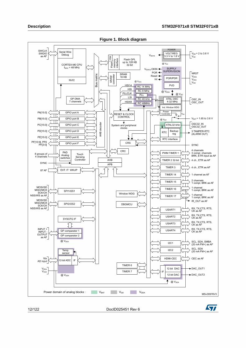
Figure 1. Block diagram

DocID025451 Rev 6 13/122
STM32F071x8 STM32F071xB Functional overview
27
3 Functional overview
Figure 1 shows the general block diagram of the STM32F071x8/xB devices.
3.1 ARM®-Cortex®-M0 core
The ARM® Cortex®-M0 is a generation of ARM 32-bit RISC processors for embedded systems. It has been developed to provide a low-cost platform that meets the needs of MCU implementation, with a reduced pin count and low-power consumption, while delivering outstanding computational performance and an advanced system response to interrupts.
The ARM® Cortex®-M0 processors feature exceptional code-efficiency, delivering the high performance expected from an ARM core, with memory sizes usually associated with 8- and 16-bit devices.
The STM32F071x8/xB devices embed ARM core and are compatible with all ARM tools and software.
3.2 Memories
The device has the following features:
• 16 Kbytes of embedded SRAM accessed (read/write) at CPU clock speed with 0 wait states and featuring embedded parity checking with exception generation for fail-critical applications.
• The non-volatile memory is divided into two arrays:
– 64 to 128 Kbytes of embedded Flash memory for programs and data
– Option bytes
The option bytes are used to write-protect the memory (with 4 KB granularity) and/or readout-protect the whole memory with the following options:
– Level 0: no readout protection
– Level 1: memory readout protection, the Flash memory cannot be read from or written to if either debug features are connected or boot in RAM is selected
– Level 2: chip readout protection, debug features (Cortex®-M0 serial wire) and boot in RAM selection disabled
3.3 Boot modes
At startup, the boot pin and boot selector option bit are used to select one of the three boot options:
• boot from User Flash memory
• boot from System Memory
• boot from embedded SRAM
The boot loader is located in System Memory. It is used to reprogram the Flash memory by using USART on pins PA14/PA15, or PA9/PA10 or I2C on pins PB6/PB7.

Functional overview STM32F071x8 STM32F071xB
14/122 DocID025451 Rev 6
3.4 Cyclic redundancy check calculation unit (CRC)
The CRC (cyclic redundancy check) calculation unit is used to get a CRC code using a configurable generator polynomial value and size.
Among other applications, CRC-based techniques are used to verify data transmission or storage integrity. In the scope of the EN/IEC 60335-1 standard, they offer a means of verifying the Flash memory integrity. The CRC calculation unit helps compute a signature of the software during runtime, to be compared with a reference signature generated at link-time and stored at a given memory location.
3.5 Power management
3.5.1 Power supply schemes
• VDD = VDDIO1 = 2.0 to 3.6 V: external power supply for I/Os (VDDIO1) and the internal regulator. It is provided externally through VDD pins.
• VDDA = from VDD to 3.6 V: external analog power supply for ADC, DAC, Reset blocks, RCs and PLL (minimum voltage to be applied to VDDA is 2.4 V when the ADC or DAC are used). It is provided externally through VDDA pin. The VDDA voltage level must be always greater or equal to the VDD voltage level and must be established first.
• VDDIO2 = 1.65 to 3.6 V: external power supply for marked I/Os. VDDIO2 is provided externally through the VDDIO2 pin. The VDDIO2 voltage level is completely independent from VDD or VDDA, but it must not be provided without a valid supply on VDD. The VDDIO2 supply is monitored and compared with the internal reference voltage (VREFINT). When the VDDIO2 is below this threshold, all the I/Os supplied from this rail are disabled by hardware. The output of this comparator is connected to EXTI line 31 and it can be used to generate an interrupt. Refer to the pinout diagrams or tables for concerned I/Os list.
• VBAT = 1.65 to 3.6 V: power supply for RTC, external clock 32 kHz oscillator and backup registers (through power switch) when VDD is not present.
For more details on how to connect power pins, refer to Figure 12: Power supply scheme.
3.5.2 Power supply supervisors
The device has integrated power-on reset (POR) and power-down reset (PDR) circuits. They are always active, and ensure proper operation above a threshold of 2 V. The device remains in reset mode when the monitored supply voltage is below a specified threshold, VPOR/PDR, without the need for an external reset circuit.
• The POR monitors only the VDD supply voltage. During the startup phase it is required that VDDA should arrive first and be greater than or equal to VDD.
• The PDR monitors both the VDD and VDDA supply voltages, however the VDDA power supply supervisor can be disabled (by programming a dedicated Option bit) to reduce the power consumption if the application design ensures that VDDA is higher than or equal to VDD.
The device features an embedded programmable voltage detector (PVD) that monitors the VDD power supply and compares it to the VPVD threshold. An interrupt can be generated when VDD drops below the VPVD threshold and/or when VDD is higher than the VPVD

DocID025451 Rev 6 15/122
STM32F071x8 STM32F071xB Functional overview
27
threshold. The interrupt service routine can then generate a warning message and/or put the MCU into a safe state. The PVD is enabled by software.
3.5.3 Voltage regulator
The regulator has two operating modes and it is always enabled after reset.
• Main (MR) is used in normal operating mode (Run).
• Low power (LPR) can be used in Stop mode where the power demand is reduced.
In Standby mode, it is put in power down mode. In this mode, the regulator output is in high impedance and the kernel circuitry is powered down, inducing zero consumption (but the contents of the registers and SRAM are lost).
3.5.4 Low-power modes
The STM32F071x8/xB microcontrollers support three low-power modes to achieve the best compromise between low power consumption, short startup time and available wakeup sources:
• Sleep mode
In Sleep mode, only the CPU is stopped. All peripherals continue to operate and can wake up the CPU when an interrupt/event occurs.
• Stop mode
Stop mode achieves very low power consumption while retaining the content of SRAM and registers. All clocks in the 1.8 V domain are stopped, the PLL, the HSI RC and the HSE crystal oscillators are disabled. The voltage regulator can also be put either in normal or in low power mode.
The device can be woken up from Stop mode by any of the EXTI lines. The EXTI line source can be one of the 16 external lines, the PVD output, RTC, I2C1, USART1, USART2, COMPx, VDDIO2 supply comparator or the CEC.
The CEC, USART1, USART2 and I2C1 peripherals can be configured to enable the HSI RC oscillator so as to get clock for processing incoming data. If this is used when the voltage regulator is put in low power mode, the regulator is first switched to normal mode before the clock is provided to the given peripheral.
• Standby mode
The Standby mode is used to achieve the lowest power consumption. The internal voltage regulator is switched off so that the entire 1.8 V domain is powered off. The PLL, the HSI RC and the HSE crystal oscillators are also switched off. After entering Standby mode, SRAM and register contents are lost except for registers in the RTC domain and Standby circuitry.
The device exits Standby mode when an external reset (NRST pin), an IWDG reset, a rising edge on the WKUP pins, or an RTC event occurs.
Note: The RTC, the IWDG, and the corresponding clock sources are not stopped by entering Stop or Standby mode.
3.6 Clocks and startup
System clock selection is performed on startup, however the internal RC 8 MHz oscillator is selected as default CPU clock on reset. An external 4-32 MHz clock can be selected, in which case it is monitored for failure. If failure is detected, the system automatically switches

Functional overview STM32F071x8 STM32F071xB
16/122 DocID025451 Rev 6
back to the internal RC oscillator. A software interrupt is generated if enabled. Similarly, full interrupt management of the PLL clock entry is available when necessary (for example on failure of an indirectly used external crystal, resonator or oscillator).
Figure 2. Clock tree
Several prescalers allow the application to configure the frequency of the AHB and the APB domains. The maximum frequency of the AHB and the APB domains is 48 MHz.

DocID025451 Rev 6 17/122
STM32F071x8 STM32F071xB Functional overview
27
Additionally, also the internal RC 48 MHz oscillator can be selected for system clock or PLL input source. This oscillator can be automatically fine-trimmed by the means of the CRS peripheral using the external synchronization.
3.7 General-purpose inputs/outputs (GPIOs)
Each of the GPIO pins can be configured by software as output (push-pull or open-drain), as input (with or without pull-up or pull-down) or as peripheral alternate function. Most of the GPIO pins are shared with digital or analog alternate functions.
The I/O configuration can be locked if needed following a specific sequence in order to avoid spurious writing to the I/Os registers.
3.8 Direct memory access controller (DMA)
The 7-channel general-purpose DMAs manage memory-to-memory, peripheral-to-memory and memory-to-peripheral transfers.
The DMA supports circular buffer management, removing the need for user code intervention when the controller reaches the end of the buffer.
Each channel is connected to dedicated hardware DMA requests, with support for software trigger on each channel. Configuration is made by software and transfer sizes between source and destination are independent.
DMA can be used with the main peripherals: SPIx, I2Sx, I2Cx, USARTx, all TIMx timers (except TIM14), DAC and ADC.
3.9 Interrupts and events
3.9.1 Nested vectored interrupt controller (NVIC)
The STM32F0xx family embeds a nested vectored interrupt controller able to handle up to 32 maskable interrupt channels (not including the 16 interrupt lines of Cortex®-M0) and 4 priority levels.
• Closely coupled NVIC gives low latency interrupt processing
• Interrupt entry vector table address passed directly to the core
• Closely coupled NVIC core interface
• Allows early processing of interrupts
• Processing of late arriving higher priority interrupts
• Support for tail-chaining
• Processor state automatically saved
• Interrupt entry restored on interrupt exit with no instruction overhead
This hardware block provides flexible interrupt management features with minimal interrupt latency.

Functional overview STM32F071x8 STM32F071xB
18/122 DocID025451 Rev 6
3.9.2 Extended interrupt/event controller (EXTI)
The extended interrupt/event controller consists of 32 edge detector lines used to generate interrupt/event requests and wake-up the system. Each line can be independently configured to select the trigger event (rising edge, falling edge, both) and can be masked independently. A pending register maintains the status of the interrupt requests. The EXTI can detect an external line with a pulse width shorter than the internal clock period. Up to 87 GPIOs can be connected to the 16 external interrupt lines.
3.10 Analog-to-digital converter (ADC)
The 12-bit analog-to-digital converter has up to 16 external and 3 internal (temperature sensor, voltage reference, VBAT voltage measurement) channels and performs conversions in single-shot or scan modes. In scan mode, automatic conversion is performed on a selected group of analog inputs.
The ADC can be served by the DMA controller.
An analog watchdog feature allows very precise monitoring of the converted voltage of one, some or all selected channels. An interrupt is generated when the converted voltage is outside the programmed thresholds.
3.10.1 Temperature sensor
The temperature sensor (TS) generates a voltage VSENSE that varies linearly with temperature.
The temperature sensor is internally connected to the ADC_IN16 input channel which is used to convert the sensor output voltage into a digital value.
The sensor provides good linearity but it has to be calibrated to obtain good overall accuracy of the temperature measurement. As the offset of the temperature sensor varies from chip to chip due to process variation, the uncalibrated internal temperature sensor is suitable for applications that detect temperature changes only.
To improve the accuracy of the temperature sensor measurement, each device is individually factory-calibrated by ST. The temperature sensor factory calibration data are stored by ST in the system memory area, accessible in read-only mode.
3.10.2 Internal voltage reference (VREFINT)
The internal voltage reference (VREFINT) provides a stable (bandgap) voltage output for the ADC and comparators. VREFINT is internally connected to the ADC_IN17 input channel. The
Table 3. Temperature sensor calibration values
Calibration value name Description Memory address
TS_CAL1TS ADC raw data acquired at a temperature of 30 °C (± 5 °C), VDDA= 3.3 V (± 10 mV)
0x1FFF F7B8 - 0x1FFF F7B9
TS_CAL2TS ADC raw data acquired at a temperature of 110 °C (± 5 °C), VDDA= 3.3 V (± 10 mV)
0x1FFF F7C2 - 0x1FFF F7C3

DocID025451 Rev 6 19/122
STM32F071x8 STM32F071xB Functional overview
27
precise voltage of VREFINT is individually measured for each part by ST during production test and stored in the system memory area. It is accessible in read-only mode.
3.10.3 VBAT battery voltage monitoring
This embedded hardware feature allows the application to measure the VBAT battery voltage using the internal ADC channel ADC_IN18. As the VBAT voltage may be higher than VDDA, and thus outside the ADC input range, the VBAT pin is internally connected to a bridge divider by 2. As a consequence, the converted digital value is half the VBAT voltage.
3.11 Digital-to-analog converter (DAC)
The two 12-bit buffered DAC channels can be used to convert digital signals into analog voltage signal outputs. The chosen design structure is composed of integrated resistor strings and an amplifier in non-inverting configuration.
This digital Interface supports the following features:
• 8-bit or 12-bit monotonic output
• Left or right data alignment in 12-bit mode
• Synchronized update capability
• Noise-wave generation
• Triangular-wave generation
• Dual DAC channel independent or simultaneous conversions
• DMA capability for each channel
• External triggers for conversion
Six DAC trigger inputs are used in the device. The DAC is triggered through the timer trigger outputs and the DAC interface is generating its own DMA requests.
3.12 Comparators (COMP)
The device embeds two fast rail-to-rail low-power comparators with programmable reference voltage (internal or external), hysteresis and speed (low speed for low power) and with selectable output polarity.
The reference voltage can be one of the following:
• External I/O
• DAC output pins
• Internal reference voltage or submultiple (1/4, 1/2, 3/4).Refer to Table 28: Embedded internal reference voltage for the value and precision of the internal reference voltage.
Table 4. Internal voltage reference calibration values
Calibration value name Description Memory address
VREFINT_CALRaw data acquired at a temperature of 30 °C (± 5 °C), VDDA= 3.3 V (± 10 mV)
0x1FFF F7BA - 0x1FFF F7BB

Functional overview STM32F071x8 STM32F071xB
20/122 DocID025451 Rev 6
Both comparators can wake up from STOP mode, generate interrupts and breaks for the timers and can be also combined into a window comparator.
3.13 Touch sensing controller (TSC)
The STM32F071x8/xB devices provide a simple solution for adding capacitive sensing functionality to any application. These devices offer up to 24 capacitive sensing channels distributed over 8 analog I/O groups.
Capacitive sensing technology is able to detect the presence of a finger near a sensor which is protected from direct touch by a dielectric (glass, plastic...). The capacitive variation introduced by the finger (or any conductive object) is measured using a proven implementation based on a surface charge transfer acquisition principle. It consists in charging the sensor capacitance and then transferring a part of the accumulated charges into a sampling capacitor until the voltage across this capacitor has reached a specific threshold. To limit the CPU bandwidth usage, this acquisition is directly managed by the hardware touch sensing controller and only requires few external components to operate. For operation, one capacitive sensing GPIO in each group is connected to an external capacitor and cannot be used as effective touch sensing channel.
The touch sensing controller is fully supported by the STMTouch touch sensing firmware library, which is free to use and allows touch sensing functionality to be implemented reliably in the end application.
Table 5. Capacitive sensing GPIOs available on STM32F071x8/xB devices
GroupCapacitive sensing
signal namePin
nameGroup
Capacitive sensing signal name
Pin name
1
TSC_G1_IO1 PA0
5
TSC_G5_IO1 PB3
TSC_G1_IO2 PA1 TSC_G5_IO2 PB4
TSC_G1_IO3 PA2 TSC_G5_IO3 PB6
TSC_G1_IO4 PA3 TSC_G5_IO4 PB7
2
TSC_G2_IO1 PA4
6
TSC_G6_IO1 PB11
TSC_G2_IO2 PA5 TSC_G6_IO2 PB12
TSC_G2_IO3 PA6 TSC_G6_IO3 PB13
TSC_G2_IO4 PA7 TSC_G6_IO4 PB14
3
TSC_G3_IO1 PC5
7
TSC_G7_IO1 PE2
TSC_G3_IO2 PB0 TSC_G7_IO2 PE3
TSC_G3_IO3 PB1 TSC_G7_IO3 PE4
TSC_G3_IO4 PB2 TSC_G7_IO4 PE5
4
TSC_G4_IO1 PA9
8
TSC_G8_IO1 PD12
TSC_G4_IO2 PA10 TSC_G8_IO2 PD13
TSC_G4_IO3 PA11 TSC_G8_IO3 PD14
TSC_G4_IO4 PA12 TSC_G8_IO4 PD15

DocID025451 Rev 6 21/122
STM32F071x8 STM32F071xB Functional overview
27
3.14 Timers and watchdogs
The STM32F071x8/xB devices include up to six general-purpose timers, two basic timers and an advanced control timer.
Table 7 compares the features of the different timers.
Table 6. Number of capacitive sensing channels available on STM32F071x8/xB devices
Analog I/O groupNumber of capacitive sensing channels
STM32F071Vx STM32F071Rx STM32F071Cx
G1 3 3 3
G2 3 3 3
G3 3 3 2
G4 3 3 3
G5 3 3 3
G6 3 3 3
G7 3 0 0
G8 3 0 0
Number of capacitive sensing channels
24 18 17
Table 7. Timer feature comparison
Timer type
TimerCounter
resolutionCounter
typePrescaler
factor
DMA request
generation
Capture/compare channels
Complementaryoutputs
Advanced control
TIM1 16-bitUp, down, up/down
integer from 1 to 65536
Yes 4 3
General purpose
TIM2 32-bitUp, down, up/down
integer from 1 to 65536
Yes 4 -
TIM3 16-bitUp, down, up/down
integer from 1 to 65536
Yes 4 -
TIM14 16-bit Upinteger from 1 to 65536
No 1 -
TIM15 16-bit Upinteger from 1 to 65536
Yes 2 1
TIM16TIM17
16-bit Upinteger from 1 to 65536
Yes 1 1
BasicTIM6TIM7
16-bit Upinteger from 1 to 65536
Yes - -

Functional overview STM32F071x8 STM32F071xB
22/122 DocID025451 Rev 6
3.14.1 Advanced-control timer (TIM1)
The advanced-control timer (TIM1) can be seen as a three-phase PWM multiplexed on six channels. It has complementary PWM outputs with programmable inserted dead times. It can also be seen as a complete general-purpose timer. The four independent channels can be used for:
• input capture
• output compare
• PWM generation (edge or center-aligned modes)
• one-pulse mode output
If configured as a standard 16-bit timer, it has the same features as the TIMx timer. If configured as the 16-bit PWM generator, it has full modulation capability (0-100%).
The counter can be frozen in debug mode.
Many features are shared with those of the standard timers which have the same architecture. The advanced control timer can therefore work together with the other timers via the Timer Link feature for synchronization or event chaining.
3.14.2 General-purpose timers (TIM2, 3, 14, 15, 16, 17)
There are six synchronizable general-purpose timers embedded in the STM32F071x8/xB devices (see Table 7 for differences). Each general-purpose timer can be used to generate PWM outputs, or as simple time base.
TIM2, TIM3
STM32F071x8/xB devices feature two synchronizable 4-channel general-purpose timers. TIM2 is based on a 32-bit auto-reload up/downcounter and a 16-bit prescaler. TIM3 is based on a 16-bit auto-reload up/downcounter and a 16-bit prescaler. They feature 4 independent channels each for input capture/output compare, PWM or one-pulse mode output. This gives up to 12 input captures/output compares/PWMs on the largest packages.
The TIM2 and TIM3 general-purpose timers can work together or with the TIM1 advanced-control timer via the Timer Link feature for synchronization or event chaining.
TIM2 and TIM3 both have independent DMA request generation.
These timers are capable of handling quadrature (incremental) encoder signals and the digital outputs from 1 to 3 hall-effect sensors.
Their counters can be frozen in debug mode.
TIM14
This timer is based on a 16-bit auto-reload upcounter and a 16-bit prescaler.
TIM14 features one single channel for input capture/output compare, PWM or one-pulse mode output.
Its counter can be frozen in debug mode.
TIM15, TIM16 and TIM17
These timers are based on a 16-bit auto-reload upcounter and a 16-bit prescaler.

DocID025451 Rev 6 23/122
STM32F071x8 STM32F071xB Functional overview
27
TIM15 has two independent channels, whereas TIM16 and TIM17 feature one single channel for input capture/output compare, PWM or one-pulse mode output.
The TIM15, TIM16 and TIM17 timers can work together, and TIM15 can also operate withTIM1 via the Timer Link feature for synchronization or event chaining.
TIM15 can be synchronized with TIM16 and TIM17.
TIM15, TIM16 and TIM17 have a complementary output with dead-time generation and independent DMA request generation.
Their counters can be frozen in debug mode.
3.14.3 Basic timers TIM6 and TIM7
These timers are mainly used for DAC trigger generation. They can also be used as generic 16-bit time bases.
3.14.4 Independent watchdog (IWDG)
The independent watchdog is based on an 8-bit prescaler and 12-bit downcounter with user-defined refresh window. It is clocked from an independent 40 kHz internal RC and as it operates independently from the main clock, it can operate in Stop and Standby modes. It can be used either as a watchdog to reset the device when a problem occurs, or as a free running timer for application timeout management. It is hardware or software configurable through the option bytes. The counter can be frozen in debug mode.
3.14.5 System window watchdog (WWDG)
The system window watchdog is based on a 7-bit downcounter that can be set as free running. It can be used as a watchdog to reset the device when a problem occurs. It is clocked from the APB clock (PCLK). It has an early warning interrupt capability and the counter can be frozen in debug mode.
3.14.6 SysTick timer
This timer is dedicated to real-time operating systems, but could also be used as a standard down counter. It features:
• a 24-bit down counter
• autoreload capability
• maskable system interrupt generation when the counter reaches 0
• programmable clock source (HCLK or HCLK/8)
3.15 Real-time clock (RTC) and backup registers
The RTC and the five backup registers are supplied through a switch that takes power either on VDD supply when present or through the VBAT pin. The backup registers are five 32-bit registers used to store 20 bytes of user application data when VDD power is not present. They are not reset by a system or power reset, or at wake up from Standby mode.

Functional overview STM32F071x8 STM32F071xB
24/122 DocID025451 Rev 6
The RTC is an independent BCD timer/counter. Its main features are the following:
• calendar with subseconds, seconds, minutes, hours (12 or 24 format), week day, date, month, year, in BCD (binary-coded decimal) format
• automatic correction for 28, 29 (leap year), 30, and 31 day of the month
• programmable alarm with wake up from Stop and Standby mode capability
• Periodic wakeup unit with programmable resolution and period.
• on-the-fly correction from 1 to 32767 RTC clock pulses. This can be used to synchronize the RTC with a master clock
• digital calibration circuit with 1 ppm resolution, to compensate for quartz crystal inaccuracy
• Three anti-tamper detection pins with programmable filter. The MCU can be woken up from Stop and Standby modes on tamper event detection
• timestamp feature which can be used to save the calendar content. This function can be triggered by an event on the timestamp pin, or by a tamper event. The MCU can be woken up from Stop and Standby modes on timestamp event detection
• reference clock detection: a more precise second source clock (50 or 60 Hz) can be used to enhance the calendar precision
The RTC clock sources can be:
• a 32.768 kHz external crystal
• a resonator or oscillator
• the internal low-power RC oscillator (typical frequency of 40 kHz)
• the high-speed external clock divided by 32
3.16 Inter-integrated circuit interface (I2C)
Up to two I2C interfaces (I2C1 and I2C2) can operate in multimaster or slave modes. Both can support Standard mode (up to 100 kbit/s), Fast mode (up to 400 kbit/s) and Fast Mode Plus (up to 1 Mbit/s) with 20 mA output drive on most of the associated I/Os.
Both support 7-bit and 10-bit addressing modes, multiple 7-bit slave addresses (two addresses, one with configurable mask). They also include programmable analog and digital noise filters.
In addition, I2C1 provides hardware support for SMBUS 2.0 and PMBUS 1.1: ARP capability, Host notify protocol, hardware CRC (PEC) generation/verification, timeouts
Table 8. Comparison of I2C analog and digital filters
Aspect Analog filter Digital filter
Pulse width of suppressed spikes
≥ 50 nsProgrammable length from 1 to 15
I2Cx peripheral clocks
Benefits Available in Stop mode–Extra filtering capability vs.
standard requirements
–Stable length
DrawbacksVariations depending on
temperature, voltage, process
Wakeup from Stop on address match is not available when digital
filter is enabled.

DocID025451 Rev 6 25/122
STM32F071x8 STM32F071xB Functional overview
27
verifications and ALERT protocol management. I2C1 also has a clock domain independent from the CPU clock, allowing the I2C1 to wake up the MCU from Stop mode on address match.
The I2C peripherals can be served by the DMA controller.
Refer to Table 9 for the differences between I2C1 and I2C2.
3.17 Universal synchronous/asynchronous receiver/transmitter (USART)
The device embeds four universal synchronous/asynchronous receivers/transmitters (USART1, USART2, USART3, USART4) which communicate at speeds of up to 6 Mbit/s.
They provide hardware management of the CTS, RTS and RS485 DE signals, multiprocessor communication mode, master synchronous communication and single-wire half-duplex communication mode. USART1 and USART2 support also SmartCard communication (ISO 7816), IrDA SIR ENDEC, LIN Master/Slave capability and auto baud rate feature, and have a clock domain independent of the CPU clock, allowing to wake up the MCU from Stop mode.
The USART interfaces can be served by the DMA controller.
Table 9. STM32F071x8/xB I2C implementation
I2C features(1)
1. X = supported.
I2C1 I2C2
7-bit addressing mode X X
10-bit addressing mode X X
Standard mode (up to 100 kbit/s) X X
Fast mode (up to 400 kbit/s) X X
Fast Mode Plus (up to 1 Mbit/s) with 20 mA output drive I/Os X X
Independent clock X -
SMBus X -
Wakeup from STOP X -
Table 10. STM32F071x8/xB USART implementation
USART modes/features(1) USART1 andUSART2
USART3 and USART4
Hardware flow control for modem X X
Continuous communication using DMA X X
Multiprocessor communication X X
Synchronous mode X X
Smartcard mode X -
Single-wire half-duplex communication X X

Functional overview STM32F071x8 STM32F071xB
26/122 DocID025451 Rev 6
3.18 Serial peripheral interface (SPI) / Inter-integrated sound interface (I2S)
Two SPIs are able to communicate up to 18 Mbit/s in slave and master modes in full-duplex and half-duplex communication modes. The 3-bit prescaler gives 8 master mode frequencies and the frame size is configurable from 4 bits to 16 bits.
Two standard I2S interfaces (multiplexed with SPI1 and SPI2 respectively) supporting four different audio standards can operate as master or slave at half-duplex communication mode. They can be configured to transfer 16 and 24 or 32 bits with 16-bit or 32-bit data resolution and synchronized by a specific signal. Audio sampling frequency from 8 kHz up to 192 kHz can be set by an 8-bit programmable linear prescaler. When operating in master mode, they can output a clock for an external audio component at 256 times the sampling frequency.
3.19 High-definition multimedia interface (HDMI) - consumer electronics control (CEC)
The device embeds a HDMI-CEC controller that provides hardware support for the Consumer Electronics Control (CEC) protocol (Supplement 1 to the HDMI standard).
This protocol provides high-level control functions between all audiovisual products in an environment. It is specified to operate at low speeds with minimum processing and memory
IrDA SIR ENDEC block X -
LIN mode X -
Dual clock domain and wakeup from Stop mode X -
Receiver timeout interrupt X -
Modbus communication X -
Auto baud rate detection X -
Driver Enable X X
1. X = supported.
Table 10. STM32F071x8/xB USART implementation (continued)
USART modes/features(1) USART1 andUSART2
USART3 and USART4
Table 11. STM32F071x8/xB SPI/I2S implementation
SPI features(1)
1. X = supported.
SPI1 and SPI2
Hardware CRC calculation X
Rx/Tx FIFO X
NSS pulse mode X
I2S mode X
TI mode X

DocID025451 Rev 6 27/122
STM32F071x8 STM32F071xB Functional overview
27
overhead. It has a clock domain independent from the CPU clock, allowing the HDMI_CEC controller to wakeup the MCU from Stop mode on data reception.
3.20 Clock recovery system (CRS)
The STM32F071x8/xB embeds a special block which allows automatic trimming of the internal 48 MHz oscillator to guarantee its optimal accuracy over the whole device operational range. This automatic trimming is based on the external synchronization signal, which could be either derived from LSE oscillator, from an external signal on CRS_SYNC pin or generated by user software. For faster lock-in during startup it is also possible to combine automatic trimming with manual trimming action.
3.21 Serial wire debug port (SW-DP)
An ARM SW-DP interface is provided to allow a serial wire debugging tool to be connected to the MCU.

Pinouts and pin descriptions STM32F071x8 STM32F071xB
28/122 DocID025451 Rev 6
4 Pinouts and pin descriptions
Figure 3. UFBGA100 package pinout

DocID025451 Rev 6 29/122
STM32F071x8 STM32F071xB Pinouts and pin descriptions
38
Figure 4. LQFP100 package pinout

Pinouts and pin descriptions STM32F071x8 STM32F071xB
30/122 DocID025451 Rev 6
Figure 5. LQFP64 package pinout
Figure 6. LQFP48 package pinout

DocID025451 Rev 6 31/122
STM32F071x8 STM32F071xB Pinouts and pin descriptions
38
Figure 7. UFQFPN48 package pinout
Figure 8. WLCSP49 package pinout
1. The above figure shows the package in top view, changing from bottom view in the previous document versions.
Pinouts and pin descriptions STM32F071x8 STM32F071xB
32/122 DocID025451 Rev 6
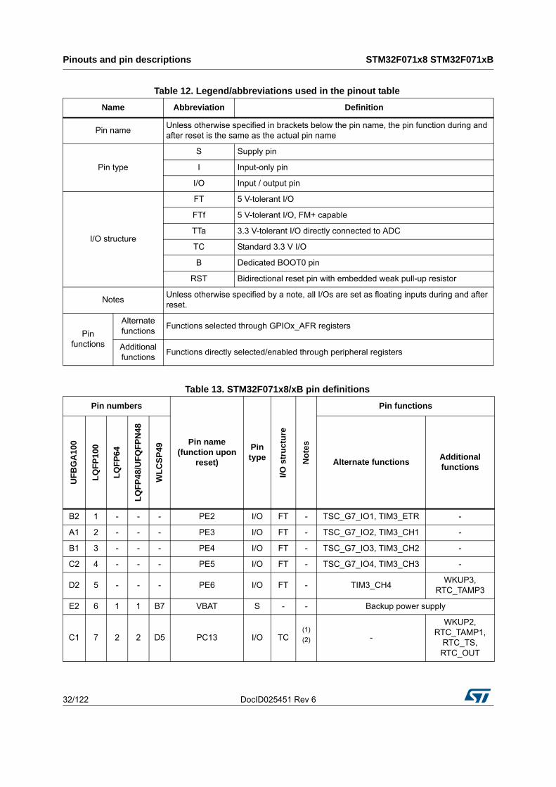
Table 12. Legend/abbreviations used in the pinout table
Name Abbreviation Definition
Pin nameUnless otherwise specified in brackets below the pin name, the pin function during and after reset is the same as the actual pin name
Pin type
S Supply pin
I Input-only pin
I/O Input / output pin
I/O structure
FT 5 V-tolerant I/O
FTf 5 V-tolerant I/O, FM+ capable
TTa 3.3 V-tolerant I/O directly connected to ADC
TC Standard 3.3 V I/O
B Dedicated BOOT0 pin
RST Bidirectional reset pin with embedded weak pull-up resistor
NotesUnless otherwise specified by a note, all I/Os are set as floating inputs during and after reset.
Pin functions
Alternate functions
Functions selected through GPIOx_AFR registers
Additional functions
Functions directly selected/enabled through peripheral registers
Table 13. STM32F071x8/xB pin definitions
Pin numbers
Pin name(function upon
reset)
Pin type
I/O s
tru
ctu
re
No
tes
Pin functions
UF
BG
A1
00
LQ
FP
100
LQ
FP
64
LQ
FP
48/
UF
QF
PN
48
WL
CS
P49
Alternate functionsAdditional functions
B2 1 - - - PE2 I/O FT - TSC_G7_IO1, TIM3_ETR -
A1 2 - - - PE3 I/O FT - TSC_G7_IO2, TIM3_CH1 -
B1 3 - - - PE4 I/O FT - TSC_G7_IO3, TIM3_CH2 -
C2 4 - - - PE5 I/O FT - TSC_G7_IO4, TIM3_CH3 -
D2 5 - - - PE6 I/O FT - TIM3_CH4WKUP3,
RTC_TAMP3
E2 6 1 1 B7 VBAT S - - Backup power supply
C1 7 2 2 D5 PC13 I/O TC(1)
(2) -
WKUP2, RTC_TAMP1,
RTC_TS, RTC_OUT

DocID025451 Rev 6 33/122
STM32F071x8 STM32F071xB Pinouts and pin descriptions
38
D1 8 3 3 C7PC14-OSC32_IN
(PC14)I/O TC
(1)
(2) - OSC32_IN
E1 9 4 4 C6PC15-
OSC32_OUT(PC15)
I/O TC(1)
(2) - OSC32_OUT
F2 10 - - - PF9 I/O FT - TIM15_CH1 -
G2 11 - - - PF10 I/O FT - TIM15_CH2 -
F1 12 5 5 D7PF0-OSC_IN
(PF0)I/O FT - CRS_ SYNC OSC_IN
G1 13 6 6 D6PF1-OSC_OUT
(PF1)I/O FT - - OSC_OUT
H2 14 7 7 E7 NRST I/O RST - Device reset input / internal reset output
(active low)
H1 15 8 - - PC0 I/O TTa - EVENTOUT ADC_IN10
J2 16 9 - - PC1 I/O TTa - EVENTOUT ADC_IN11
J3 17 10 - - PC2 I/O TTa -SPI2_MISO, I2S2_MCK,
EVENTOUTADC_IN12
K2 18 11 - - PC3 I/O TTa -SPI2_MOSI, I2S2_SD,
EVENTOUTADC_IN13
J1 19 - - - PF2 I/O FT - EVENTOUT WKUP8
K1 20 12 8 E6 VSSA S - - Analog ground
M1 21 13 9 F7 VDDA S - - Analog power supply
L1 22 - - - PF3 I/O FT - EVENTOUT
L2 23 14 10 F6 PA0 I/O TTa -
USART2_CTS, TIM2_CH1_ETR,
TSC_G1_IO1, USART4_TX
RTC_ TAMP2,WKUP1,
COMP1_OUT,ADC_IN0,
COMP1_INM6
M2 24 15 11 G7 PA1 I/O TTa -
USART2_RTS, TIM2_CH2,TIM15_CH1N, TSC_G1_IO2,
USART4_RX, EVENTOUT
ADC_IN1,COMP1_INP
Table 13. STM32F071x8/xB pin definitions (continued)
Pin numbers
Pin name(function upon
reset)
Pin type
I/O s
tru
ctu
re
No
tes
Pin functions
UF
BG
A1
00
LQ
FP
100
LQ
FP
64
LQ
FP
48/U
FQ
FP
N48
WL
CS
P49
Alternate functionsAdditional functions

Pinouts and pin descriptions STM32F071x8 STM32F071xB
34/122 DocID025451 Rev 6
K3 25 16 12 E5 PA2 I/O TTa -USART2_TX, TIM2_CH3,
TIM15_CH1, TSC_G1_IO3
ADC_IN2,COMP2_OUT,COMP2_INM6,
WKUP4
L3 26 17 13 E4 PA3 I/O TTa -USART2_RX,TIM2_CH4,
TIM15_CH2, TSC_G1_IO4ADC_IN3,
COMP2_INP
D3 27 18 - - VSS S - - Ground
H3 28 19 - - VDD S - - Digital power supply
M3 29 20 14 G6 PA4 I/O TTa -SPI1_NSS, I2S1_WS,
TIM14_CH1, TSC_G2_IO1,USART2_CK
COMP1_INM4,COMP2_INM4,
ADC_IN4,DAC_OUT1
K4 30 21 15 F5 PA5 I/O TTa -SPI1_SCK, I2S1_CK, CEC,
TIM2_CH1_ETR, TSC_G2_IO2
COMP1_INM5,COMP2_INM5,
ADC_IN5,DAC_OUT2
L4 31 22 16 F4 PA6 I/O TTa -
SPI1_MISO, I2S1_MCK,TIM3_CH1, TIM1_BKIN,
TIM16_CH1, COMP1_OUT,
TSC_G2_IO3, EVENTOUT,USART3_CTS
ADC_IN6
M4 32 23 17 F3 PA7 I/O TTa -
SPI1_MOSI, I2S1_SD,TIM3_CH2, TIM14_CH1,
TIM1_CH1N, TIM17_CH1,COMP2_OUT, TSC_G2_IO4,EVENTOUT
ADC_IN7
K5 33 24 - - PC4 I/O TTa - EVENTOUT, USART3_TX ADC_IN14
L5 34 25 - - PC5 I/O TTa -TSC_G3_IO1, USART3_RX
ADC_IN15,WKUP5
M5 35 26 18 G5 PB0 I/O TTa -TIM3_CH3, TIM1_CH2N,
TSC_G3_IO2, EVENTOUT,USART3_CK
ADC_IN8
M6 36 27 19 G4 PB1 I/O TTa -TIM3_CH4, USART3_RTS,TIM14_CH1, TIM1_CH3N,
TSC_G3_IO3ADC_IN9
L6 37 28 20 G3 PB2 I/O FT TSC_G3_IO4 -
Table 13. STM32F071x8/xB pin definitions (continued)
Pin numbers
Pin name(function upon
reset)
Pin type
I/O s
tru
ctu
re
No
tes
Pin functions
UF
BG
A1
00
LQ
FP
100
LQ
FP
64
LQ
FP
48/U
FQ
FP
N48
WL
CS
P49
Alternate functionsAdditional functions
DocID025451 Rev 6 35/122
STM32F071x8 STM32F071xB Pinouts and pin descriptions
38
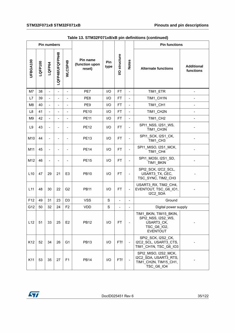
M7 38 - - - PE7 I/O FT - TIM1_ETR -
L7 39 - - - PE8 I/O FT - TIM1_CH1N -
M8 40 - - - PE9 I/O FT - TIM1_CH1 -
L8 41 - - - PE10 I/O FT - TIM1_CH2N -
M9 42 - - - PE11 I/O FT - TIM1_CH2 -
L9 43 - - - PE12 I/O FT -SPI1_NSS, I2S1_WS,
TIM1_CH3N-
M10 44 - - - PE13 I/O FT -SPI1_SCK, I2S1_CK,
TIM1_CH3-
M11 45 - - - PE14 I/O FT -SPI1_MISO, I2S1_MCK,
TIM1_CH4-
M12 46 - - - PE15 I/O FT -SPI1_MOSI, I2S1_SD,
TIM1_BKIN-
L10 47 29 21 E3 PB10 I/O FT -SPI2_SCK, I2C2_SCL,
USART3_TX, CEC,TSC_SYNC, TIM2_CH3
-
L11 48 30 22 G2 PB11 I/O FT -USART3_RX, TIM2_CH4,
EVENTOUT, TSC_G6_IO1,I2C2_SDA
-
F12 49 31 23 D3 VSS S - - Ground
G12 50 32 24 F2 VDD S - - Digital power supply
L12 51 33 25 E2 PB12 I/O FT -
TIM1_BKIN, TIM15_BKIN,SPI2_NSS, I2S2_WS,
USART3_CK, TSC_G6_IO2,EVENTOUT
-
K12 52 34 26 G1 PB13 I/O FTf -SPI2_SCK, I2S2_CK,
I2C2_SCL, USART3_CTS,TIM1_CH1N, TSC_G6_IO3
-
K11 53 35 27 F1 PB14 I/O FTf -
SPI2_MISO, I2S2_MCK,I2C2_SDA, USART3_RTS,TIM1_CH2N, TIM15_CH1,
TSC_G6_IO4
-
Table 13. STM32F071x8/xB pin definitions (continued)
Pin numbers
Pin name(function upon
reset)
Pin type
I/O s
tru
ctu
re
No
tes
Pin functions
UF
BG
A1
00
LQ
FP
100
LQ
FP
64
LQ
FP
48/U
FQ
FP
N48
WL
CS
P49
Alternate functionsAdditional functions
Pinouts and pin descriptions STM32F071x8 STM32F071xB
36/122 DocID025451 Rev 6
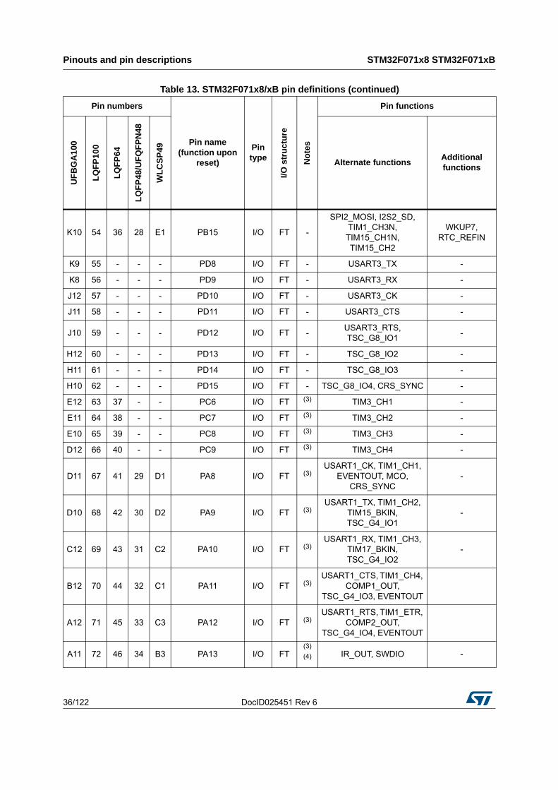
K10 54 36 28 E1 PB15 I/O FT -
SPI2_MOSI, I2S2_SD,TIM1_CH3N,
TIM15_CH1N,TIM15_CH2
WKUP7,RTC_REFIN
K9 55 - - - PD8 I/O FT - USART3_TX -
K8 56 - - - PD9 I/O FT - USART3_RX -
J12 57 - - - PD10 I/O FT - USART3_CK -
J11 58 - - - PD11 I/O FT - USART3_CTS -
J10 59 - - - PD12 I/O FT -USART3_RTS, TSC_G8_IO1
-
H12 60 - - - PD13 I/O FT - TSC_G8_IO2 -
H11 61 - - - PD14 I/O FT - TSC_G8_IO3 -
H10 62 - - - PD15 I/O FT - TSC_G8_IO4, CRS_SYNC -
E12 63 37 - - PC6 I/O FT (3) TIM3_CH1 -
E11 64 38 - - PC7 I/O FT (3) TIM3_CH2 -
E10 65 39 - - PC8 I/O FT (3) TIM3_CH3 -
D12 66 40 - - PC9 I/O FT (3) TIM3_CH4 -
D11 67 41 29 D1 PA8 I/O FT (3)USART1_CK, TIM1_CH1,
EVENTOUT, MCO,CRS_SYNC
-
D10 68 42 30 D2 PA9 I/O FT (3)USART1_TX, TIM1_CH2,
TIM15_BKIN, TSC_G4_IO1
-
C12 69 43 31 C2 PA10 I/O FT (3)USART1_RX, TIM1_CH3,
TIM17_BKIN, TSC_G4_IO2
-
B12 70 44 32 C1 PA11 I/O FT (3)USART1_CTS, TIM1_CH4,
COMP1_OUT, TSC_G4_IO3, EVENTOUT
A12 71 45 33 C3 PA12 I/O FT (3)USART1_RTS, TIM1_ETR,
COMP2_OUT, TSC_G4_IO4, EVENTOUT
A11 72 46 34 B3 PA13 I/O FT(3)
(4) IR_OUT, SWDIO -
Table 13. STM32F071x8/xB pin definitions (continued)
Pin numbers
Pin name(function upon
reset)
Pin type
I/O s
tru
ctu
re
No
tes
Pin functions
UF
BG
A1
00
LQ
FP
100
LQ
FP
64
LQ
FP
48/U
FQ
FP
N48
WL
CS
P49
Alternate functionsAdditional functions

DocID025451 Rev 6 37/122
STM32F071x8 STM32F071xB Pinouts and pin descriptions
38
C11 73 - - - PF6 I/O FT (3) - -
F11 74 47 35 B1 VSS S - - Ground
G11 75 48 36 B2 VDDIO2 S - - Digital power supply
A10 76 49 37 A1 PA14 I/O FT(3)
(4) USART2_TX, SWCLK -
A9 77 50 38 A2 PA15 I/O FT (3)
SPI1_NSS, I2S1_WS,USART2_RX,
USART4_RTS, TIM2_CH1_ETR,
EVENTOUT
-
B11 78 51 - - PC10 I/O FT (3) USART3_TX, USART4_TX -
C10 79 52 - - PC11 I/O FT (3) USART3_RX, USART4_RX -
B10 80 53 - - PC12 I/O FT (3) USART3_CK,USART4_CK
-
C9 81 - - - PD0 I/O FT (3) SPI2_NSS, I2S2_WS -
B9 82 - - - PD1 I/O FT (3) SPI2_SCK, I2S2_CK -
C8 83 54 - - PD2 I/O FT (3) USART3_RTS, TIM3_ETR -
B8 84 - - - PD3 I/O FT -SPI2_MISO, I2S2_MCK,
USART2_CTS-
B7 85 - - - PD4 I/O FT -SPI2_MOSI, I2S2_SD,
USART2_RTS-
A6 86 - - - PD5 I/O FT - USART2_TX -
B6 87 - - - PD6 I/O FT - USART2_RX -
A5 88 - - - PD7 I/O FT - USART2_CK -
A8 89 55 39 A3 PB3 I/O FT -SPI1_SCK, I2S1_CK,
TIM2_CH2, TSC_G5_IO1,EVENTOUT
-
A7 90 56 40 A4 PB4 I/O FT -SPI1_MISO, I2S1_MCK,TIM17_BKIN, TIM3_CH1,
TSC_G5_IO2, EVENTOUT -
C5 91 57 41 B4 PB5 I/O FT -SPI1_MOSI, I2S1_SD,
I2C1_SMBA, TIM16_BKIN,TIM3_CH2
WKUP6
Table 13. STM32F071x8/xB pin definitions (continued)
Pin numbers
Pin name(function upon
reset)
Pin type
I/O s
tru
ctu
re
No
tes
Pin functions
UF
BG
A1
00
LQ
FP
100
LQ
FP
64
LQ
FP
48/U
FQ
FP
N48
WL
CS
P49
Alternate functionsAdditional functions

Pinouts and pin descriptions STM32F071x8 STM32F071xB
38/122 DocID025451 Rev 6
B5 92 58 42 C4 PB6 I/O FTf -I2C1_SCL, USART1_TX,
TIM16_CH1N, TSC_G5_I03
-
B4 93 59 43 D4 PB7 I/O FTf -
I2C1_SDA, USART1_RX,USART4_CTS, TIM17_CH1N, TSC_G5_IO4
-
A4 94 60 44 A5 BOOT0 I B - Boot memory selection
A3 95 61 45 B5 PB8 I/O FTf -I2C1_SCL, CEC,
TIM16_CH1, TSC_SYNC-
B3 96 62 46 C5 PB9 I/O FTf -SPI2_NSS, I2S2_WS,I2C1_SDA, IR_OUT,
TIM17_CH1, EVENTOUT-
C3 97 - - - PE0 I/O FT - EVENTOUT, TIM16_CH1 -
A2 98 - - - PE1 I/O FT - EVENTOUT, TIM17_CH1 -
D3 99 63 47 A6 VSS S - - Ground
C4 100 64 48 A7 VDD S - - Digital power supply
1. PC13, PC14 and PC15 are supplied through the power switch. Since the switch only sinks a limited amount of current (3 mA), the use of GPIOs PC13 to PC15 in output mode is limited: - The speed should not exceed 2 MHz with a maximum load of 30 pF. - These GPIOs must not be used as current sources (e.g. to drive an LED).
2. After the first RTC domain power-up, PC13, PC14 and PC15 operate as GPIOs. Their function then depends on the content of the RTC registers which are not reset by the system reset. For details on how to manage these GPIOs, refer to the RTC domain and RTC register descriptions in the reference manual.
3. PC6, PC7, PC8, PC9, PA8, PA9, PA10, PA11, PA12, PA13, PF6, PA14, PA15, PC10, PC11, PC12, PD0, PD1 and PD2 I/Os are supplied by VDDIO2.
4. After reset, these pins are configured as SWDIO and SWCLK alternate functions, and the internal pull-up on the SWDIO pin and the internal pull-down on the SWCLK pin are activated.
Table 13. STM32F071x8/xB pin definitions (continued)
Pin numbers
Pin name(function upon
reset)
Pin type
I/O s
tru
ctu
re
No
tes
Pin functions
UF
BG
A1
00
LQ
FP
100
LQ
FP
64
LQ
FP
48/U
FQ
FP
N48
WL
CS
P49
Alternate functionsAdditional functions
ST
M3
2F0
71x8
ST
M3
2F0
71xB
DocID
025451 R
ev 6
39/122
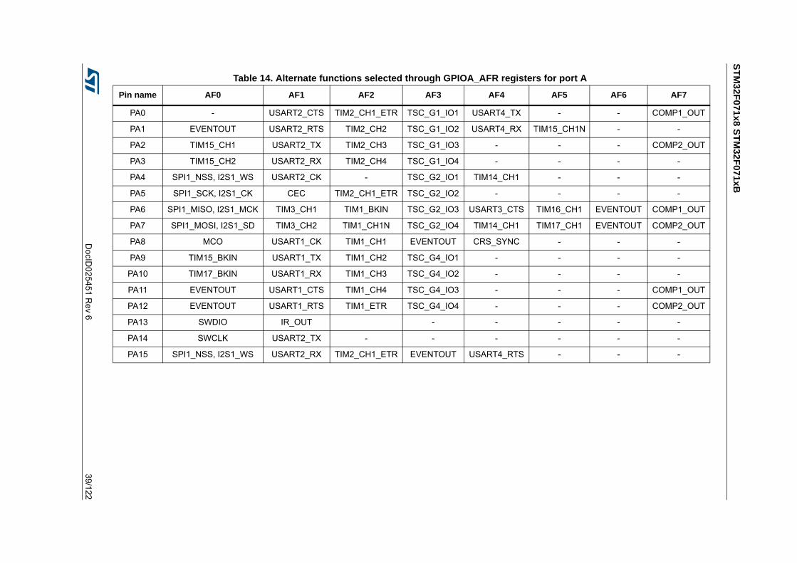
Table 14. Alternate functions selected through GPIOA_AFR registers for port A
Pin name AF0 AF1 AF2 AF3 AF4 AF5 AF6 AF7
PA0 - USART2_CTS TIM2_CH1_ETR TSC_G1_IO1 USART4_TX - - COMP1_OUT
PA1 EVENTOUT USART2_RTS TIM2_CH2 TSC_G1_IO2 USART4_RX TIM15_CH1N - -
PA2 TIM15_CH1 USART2_TX TIM2_CH3 TSC_G1_IO3 - - - COMP2_OUT
PA3 TIM15_CH2 USART2_RX TIM2_CH4 TSC_G1_IO4 - - - -
PA4 SPI1_NSS, I2S1_WS USART2_CK - TSC_G2_IO1 TIM14_CH1 - - -
PA5 SPI1_SCK, I2S1_CK CEC TIM2_CH1_ETR TSC_G2_IO2 - - - -
PA6 SPI1_MISO, I2S1_MCK TIM3_CH1 TIM1_BKIN TSC_G2_IO3 USART3_CTS TIM16_CH1 EVENTOUT COMP1_OUT
PA7 SPI1_MOSI, I2S1_SD TIM3_CH2 TIM1_CH1N TSC_G2_IO4 TIM14_CH1 TIM17_CH1 EVENTOUT COMP2_OUT
PA8 MCO USART1_CK TIM1_CH1 EVENTOUT CRS_SYNC - - -
PA9 TIM15_BKIN USART1_TX TIM1_CH2 TSC_G4_IO1 - - - -
PA10 TIM17_BKIN USART1_RX TIM1_CH3 TSC_G4_IO2 - - - -
PA11 EVENTOUT USART1_CTS TIM1_CH4 TSC_G4_IO3 - - - COMP1_OUT
PA12 EVENTOUT USART1_RTS TIM1_ETR TSC_G4_IO4 - - - COMP2_OUT
PA13 SWDIO IR_OUT - - - - -
PA14 SWCLK USART2_TX - - - - - -
PA15 SPI1_NSS, I2S1_WS USART2_RX TIM2_CH1_ETR EVENTOUT USART4_RTS - - -
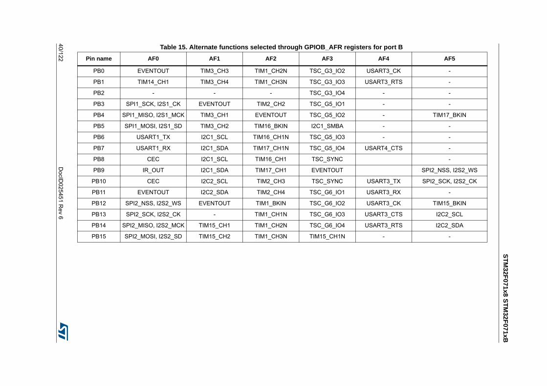
ST
M3
2F0
71x8
ST
M3
2F0
71xB
40/1
22D
ocID025
451 Re
v 6
Table 15. Alternate functions selected through GPIOB_AFR registers for port B
Pin name AF0 AF1 AF2 AF3 AF4 AF5
PB0 EVENTOUT TIM3_CH3 TIM1_CH2N TSC_G3_IO2 USART3_CK -
PB1 TIM14_CH1 TIM3_CH4 TIM1_CH3N TSC_G3_IO3 USART3_RTS -
PB2 - - - TSC_G3_IO4 - -
PB3 SPI1_SCK, I2S1_CK EVENTOUT TIM2_CH2 TSC_G5_IO1 - -
PB4 SPI1_MISO, I2S1_MCK TIM3_CH1 EVENTOUT TSC_G5_IO2 - TIM17_BKIN
PB5 SPI1_MOSI, I2S1_SD TIM3_CH2 TIM16_BKIN I2C1_SMBA - -
PB6 USART1_TX I2C1_SCL TIM16_CH1N TSC_G5_IO3 - -
PB7 USART1_RX I2C1_SDA TIM17_CH1N TSC_G5_IO4 USART4_CTS -
PB8 CEC I2C1_SCL TIM16_CH1 TSC_SYNC -
PB9 IR_OUT I2C1_SDA TIM17_CH1 EVENTOUT SPI2_NSS, I2S2_WS
PB10 CEC I2C2_SCL TIM2_CH3 TSC_SYNC USART3_TX SPI2_SCK, I2S2_CK
PB11 EVENTOUT I2C2_SDA TIM2_CH4 TSC_G6_IO1 USART3_RX -
PB12 SPI2_NSS, I2S2_WS EVENTOUT TIM1_BKIN TSC_G6_IO2 USART3_CK TIM15_BKIN
PB13 SPI2_SCK, I2S2_CK - TIM1_CH1N TSC_G6_IO3 USART3_CTS I2C2_SCL
PB14 SPI2_MISO, I2S2_MCK TIM15_CH1 TIM1_CH2N TSC_G6_IO4 USART3_RTS I2C2_SDA
PB15 SPI2_MOSI, I2S2_SD TIM15_CH2 TIM1_CH3N TIM15_CH1N - -

DocID025451 Rev 6 41/122
STM32F071x8 STM32F071xB
42
Table 16. Alternate functions selected through GPIOC_AFR registers for port C
Pin name AF0 AF1
PC0 EVENTOUT -
PC1 EVENTOUT -
PC2 EVENTOUT SPI2_MISO, I2S2_MCK
PC3 EVENTOUT SPI2_MOSI, I2S2_SD
PC4 EVENTOUT USART3_TX
PC5 TSC_G3_IO1 USART3_RX
PC6 TIM3_CH1 -
PC7 TIM3_CH2 -
PC8 TIM3_CH3 -
PC9 TIM3_CH4 -
PC10 USART4_TX USART3_TX
PC11 USART4_RX USART3_RX
PC12 USART4_CK USART3_CK
PC13 - -
PC14 - -
PC15 - -
Table 17. Alternate functions selected through GPIOD_AFR registers for port D
Pin name AF0 AF1
PD0 - SPI2_NSS, I2S2_WS
PD1 - SPI2_SCK, I2S2_CK
PD2 TIM3_ETR USART3_RTS
PD3 USART2_CTS SPI2_MISO, I2S2_MCK
PD4 USART2_RTS SPI2_MOSI, I2S2_SD
PD5 USART2_TX -
PD6 USART2_RX -
PD7 USART2_CK -
PD8 USART3_TX -
PD9 USART3_RX -
PD10 USART3_CK -
PD11 USART3_CTS -
PD12 USART3_RTS TSC_G8_IO1
PD13 - TSC_G8_IO2
PD14 - TSC_G8_IO3
PD15 CRS_SYNC TSC_G8_IO4
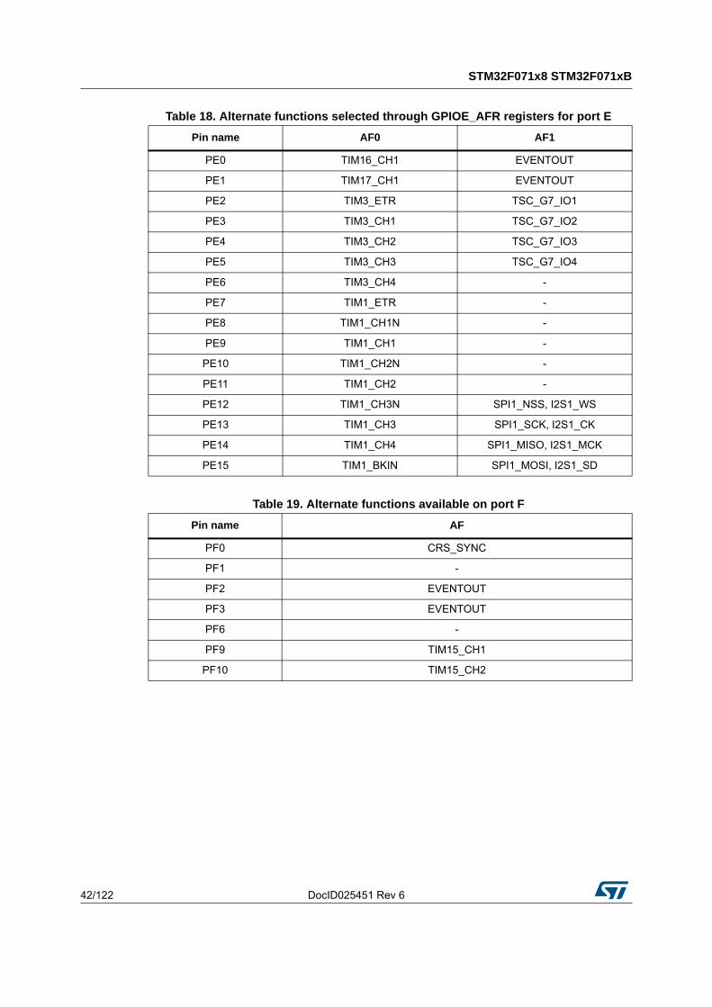
STM32F071x8 STM32F071xB
42/122 DocID025451 Rev 6
Table 18. Alternate functions selected through GPIOE_AFR registers for port E
Pin name AF0 AF1
PE0 TIM16_CH1 EVENTOUT
PE1 TIM17_CH1 EVENTOUT
PE2 TIM3_ETR TSC_G7_IO1
PE3 TIM3_CH1 TSC_G7_IO2
PE4 TIM3_CH2 TSC_G7_IO3
PE5 TIM3_CH3 TSC_G7_IO4
PE6 TIM3_CH4 -
PE7 TIM1_ETR -
PE8 TIM1_CH1N -
PE9 TIM1_CH1 -
PE10 TIM1_CH2N -
PE11 TIM1_CH2 -
PE12 TIM1_CH3N SPI1_NSS, I2S1_WS
PE13 TIM1_CH3 SPI1_SCK, I2S1_CK
PE14 TIM1_CH4 SPI1_MISO, I2S1_MCK
PE15 TIM1_BKIN SPI1_MOSI, I2S1_SD
Table 19. Alternate functions available on port F
Pin name AF
PF0 CRS_SYNC
PF1 -
PF2 EVENTOUT
PF3 EVENTOUT
PF6 -
PF9 TIM15_CH1
PF10 TIM15_CH2

DocID025451 Rev 6 43/122
STM32F071x8 STM32F071xB Memory mapping
45
5 Memory mapping
To the difference of STM32F071xB memory map in Figure 9, the two bottom code memory spaces of STM32F071x8 end at 0x0000 FFFF and 0x0800 FFFF, respectively.
Figure 9. STM32F071xB memory map

Memory mapping STM32F071x8 STM32F071xB
44/122 DocID025451 Rev 6
Table 20. STM32F071x8/xB peripheral register boundary addresses
Bus Boundary address Size Peripheral
0x4800 1800 - 0x5FFF FFFF ~384 MB Reserved
AHB2
0x4800 1400 - 0x4800 17FF 1 KB GPIOF
0x4800 1000 - 0x4800 13FF 1 KB GPIOE
0x4800 0C00 - 0x4800 0FFF 1 KB GPIOD
0x4800 0800 - 0x4800 0BFF 1 KB GPIOC
0x4800 0400 - 0x4800 07FF 1 KB GPIOB
0x4800 0000 - 0x4800 03FF 1 KB GPIOA
0x4002 4400 - 0x47FF FFFF ~128 MB Reserved
AHB1
0x4002 4000 - 0x4002 43FF 1 KB TSC
0x4002 3400 - 0x4002 3FFF 3 KB Reserved
0x4002 3000 - 0x4002 33FF 1 KB CRC
0x4002 2400 - 0x4002 2FFF 3 KB Reserved
0x4002 2000 - 0x4002 23FF 1 KB Flash memory interface
0x4002 1400 - 0x4002 1FFF 3 KB Reserved
0x4002 1000 - 0x4002 13FF 1 KB RCC
0x4002 0400 - 0x4002 0FFF 3 KB Reserved
0x4002 0000 - 0x4002 03FF 1 KB DMA
0x4001 8000 - 0x4001 FFFF 32 KB Reserved
APB
0x4001 5C00 - 0x4001 7FFF 9 KB Reserved
0x4001 5800 - 0x4001 5BFF 1 KB DBGMCU
0x4001 4C00 - 0x4001 57FF 3 KB Reserved
0x4001 4800 - 0x4001 4BFF 1 KB TIM17
0x4001 4400 - 0x4001 47FF 1 KB TIM16
0x4001 4000 - 0x4001 43FF 1 KB TIM15
0x4001 3C00 - 0x4001 3FFF 1 KB Reserved
0x4001 3800 - 0x4001 3BFF 1 KB USART1
0x4001 3400 - 0x4001 37FF 1 KB Reserved
0x4001 3000 - 0x4001 33FF 1 KB SPI1/I2S1
0x4001 2C00 - 0x4001 2FFF 1 KB TIM1
0x4001 2800 - 0x4001 2BFF 1 KB Reserved
0x4001 2400 - 0x4001 27FF 1 KB ADC
0x4001 0800 - 0x4001 23FF 7 KB Reserved
0x4001 0400 - 0x4001 07FF 1 KB EXTI
0x4001 0000 - 0x4001 03FF 1 KB SYSCFG + COMP
0x4000 8000 - 0x4000 FFFF 32 KB Reserved

DocID025451 Rev 6 45/122
STM32F071x8 STM32F071xB Memory mapping
45
APB
0x4000 7C00 - 0x4000 7FFF 1 KB Reserved
0x4000 7800 - 0x4000 7BFF 1 KB CEC
0x4000 7400 - 0x4000 77FF 1 KB DAC
0x4000 7000 - 0x4000 73FF 1 KB PWR
0x4000 6C00 - 0x4000 6FFF 1 KB CRS
0x4000 5C00 - 0x4000 6BFF 4 KB Reserved
0x4000 5800 - 0x4000 5BFF 1 KB I2C2
0x4000 5400 - 0x4000 57FF 1 KB I2C1
0x4000 5000 - 0x4000 53FF 1 KB Reserved
0x4000 4C00 - 0x4000 4FFF 1 KB USART4
0x4000 4800 - 0x4000 4BFF 1 KB USART3
0x4000 4400 - 0x4000 47FF 1 KB USART2
0x4000 3C00 - 0x4000 43FF 2 KB Reserved
0x4000 3800 - 0x4000 3BFF 1 KB SPI2
0x4000 3400 - 0x4000 37FF 1 KB Reserved
0x4000 3000 - 0x4000 33FF 1 KB IWDG
0x4000 2C00 - 0x4000 2FFF 1 KB WWDG
0x4000 2800 - 0x4000 2BFF 1 KB RTC
0x4000 2400 - 0x4000 27FF 1 KB Reserved
0x4000 2000 - 0x4000 23FF 1 KB TIM14
0x4000 1800 - 0x4000 1FFF 2 KB Reserved
0x4000 1400 - 0x4000 17FF 1 KB TIM7
0x4000 1000 - 0x4000 13FF 1 KB TIM6
0x4000 0800 - 0x4000 0FFF 2 KB Reserved
0x4000 0400 - 0x4000 07FF 1 KB TIM3
0x4000 0000 - 0x4000 03FF 1 KB TIM2
Table 20. STM32F071x8/xB peripheral register boundary addresses (continued)
Bus Boundary address Size Peripheral

Electrical characteristics STM32F071x8 STM32F071xB
46/122 DocID025451 Rev 6
6 Electrical characteristics
6.1 Parameter conditions
Unless otherwise specified, all voltages are referenced to VSS.
6.1.1 Minimum and maximum values
Unless otherwise specified, the minimum and maximum values are guaranteed in the worst conditions of ambient temperature, supply voltage and frequencies by tests in production on 100% of the devices with an ambient temperature at TA = 25 °C and TA = TAmax (given by the selected temperature range).
Data based on characterization results, design simulation and/or technology characteristics are indicated in the table footnotes and are not tested in production. Based on characterization, the minimum and maximum values refer to sample tests and represent the mean value plus or minus three times the standard deviation (mean ±3σ).
6.1.2 Typical values
Unless otherwise specified, typical data are based on TA = 25 °C, VDD = VDDA = 3.3 V. They are given only as design guidelines and are not tested.
Typical ADC accuracy values are determined by characterization of a batch of samples from a standard diffusion lot over the full temperature range, where 95% of the devices have an error less than or equal to the value indicated (mean ±2σ).
6.1.3 Typical curves
Unless otherwise specified, all typical curves are given only as design guidelines and are not tested.
6.1.4 Loading capacitor
The loading conditions used for pin parameter measurement are shown in Figure 10.
6.1.5 Pin input voltage
The input voltage measurement on a pin of the device is described in Figure 11.
Figure 10. Pin loading conditions Figure 11. Pin input voltage
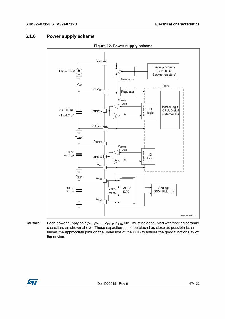
DocID025451 Rev 6 47/122
STM32F071x8 STM32F071xB Electrical characteristics
96
6.1.6 Power supply scheme
Figure 12. Power supply scheme
Caution: Each power supply pair (VDD/VSS, VDDA/VSSA etc.) must be decoupled with filtering ceramic capacitors as shown above. These capacitors must be placed as close as possible to, or below, the appropriate pins on the underside of the PCB to ensure the good functionality of the device.

Electrical characteristics STM32F071x8 STM32F071xB
48/122 DocID025451 Rev 6
6.1.7 Current consumption measurement
Figure 13. Current consumption measurement scheme

DocID025451 Rev 6 49/122
STM32F071x8 STM32F071xB Electrical characteristics
96
6.2 Absolute maximum ratings
Stresses above the absolute maximum ratings listed in Table 21: Voltage characteristics, Table 22: Current characteristics and Table 23: Thermal characteristics may cause permanent damage to the device. These are stress ratings only and functional operation of the device at these conditions is not implied. Exposure to maximum rating conditions for extended periods may affect device reliability.
Table 21. Voltage characteristics(1)
1. All main power (VDD, VDDA) and ground (VSS, VSSA) pins must always be connected to the external power supply, in the permitted range.
Symbol Ratings Min Max Unit
VDD–VSS External main supply voltage - 0.3 4.0 V
VDDIO2–VSS External I/O supply voltage - 0.3 4.0 V
VDDA–VSS External analog supply voltage - 0.3 4.0 V
VDD–VDDA Allowed voltage difference for VDD > VDDA - 0.4 V
VBAT–VSS External backup supply voltage - 0.3 4.0 V
VIN(2)
2. VIN maximum must always be respected. Refer to Table 22: Current characteristics for the maximum allowed injected current values.
Input voltage on FT and FTf pins VSS - 0.3 VDDIOx + 4.0(3)
3. Valid only if the internal pull-up/pull-down resistors are disabled. If internal pull-up or pull-down resistor is enabled, the maximum limit is 4 V.
V
Input voltage on TTa pins VSS - 0.3 4.0 V
BOOT0 0 9.0 V
Input voltage on any other pin VSS - 0.3 4.0 V
|∆VDDx| Variations between different VDD power pins - 50 mV
|VSSx - VSS|Variations between all the different ground pins
- 50 mV
VESD(HBM)Electrostatic discharge voltage (human body model)
see Section 6.3.12: Electrical sensitivity characteristics
-

Electrical characteristics STM32F071x8 STM32F071xB
50/122 DocID025451 Rev 6
Table 22. Current characteristics
Symbol Ratings Max. Unit
ΣIVDD Total current into sum of all VDD power lines (source)(1) 120
mA
ΣIVSS Total current out of sum of all VSS ground lines (sink)(1) -120
IVDD(PIN) Maximum current into each VDD power pin (source)(1) 100
IVSS(PIN) Maximum current out of each VSS ground pin (sink)(1) -100
IIO(PIN)
Output current sunk by any I/O and control pin 25
Output current source by any I/O and control pin -25
ΣIIO(PIN)
Total output current sunk by sum of all I/Os and control pins(2) 80
Total output current sourced by sum of all I/Os and control pins(2) -80
Total output current sourced by sum of all I/Os supplied by VDDIO2 -40
IINJ(PIN)(3)
Injected current on B, FT and FTf pins -5/+0(4)
Injected current on TC and RST pin ± 5
Injected current on TTa pins(5) ± 5
ΣIINJ(PIN) Total injected current (sum of all I/O and control pins)(6) ± 25
1. All main power (VDD, VDDA) and ground (VSS, VSSA) pins must always be connected to the external power supply, in the permitted range.
2. This current consumption must be correctly distributed over all I/Os and control pins. The total output current must not be sunk/sourced between two consecutive power supply pins referring to high pin count QFP packages.
3. A positive injection is induced by VIN > VDDIOx while a negative injection is induced by VIN < VSS. IINJ(PIN) must never be exceeded. Refer to Table 21: Voltage characteristics for the maximum allowed input voltage values.
4. Positive injection is not possible on these I/Os and does not occur for input voltages lower than the specified maximum value.
5. On these I/Os, a positive injection is induced by VIN > VDDA. Negative injection disturbs the analog performance of the device. See note (2) below Table 59: ADC accuracy.
6. When several inputs are submitted to a current injection, the maximum ΣIINJ(PIN) is the absolute sum of the positive and negative injected currents (instantaneous values).
Table 23. Thermal characteristics
Symbol Ratings Value Unit
TSTG Storage temperature range –65 to +150 °C
TJ Maximum junction temperature 150 °C

DocID025451 Rev 6 51/122
STM32F071x8 STM32F071xB Electrical characteristics
96
6.3 Operating conditions
6.3.1 General operating conditions
6.3.2 Operating conditions at power-up / power-down
The parameters given in Table 25 are derived from tests performed under the ambient temperature condition summarized in Table 24.
Table 24. General operating conditions
Symbol Parameter Conditions Min Max Unit
fHCLK Internal AHB clock frequency - 0 48MHz
fPCLK Internal APB clock frequency - 0 48
VDD Standard operating voltage - 2.0 3.6 V
VDDIO2 I/O supply voltageMust not be supplied if VDD is not present
1.65 3.6 V
VDDA
Analog operating voltage (ADC and DAC not used) Must have a potential equal
to or higher than VDD
VDD 3.6
VAnalog operating voltage (ADC and DAC used)
2.4 3.6
VBAT Backup operating voltage - 1.65 3.6 V
VIN I/O input voltage
TC and RST I/O –0.3 VDDIOx+0.3
VTTa I/O –0.3 VDDA+0.3(1)
FT and FTf I/O –0.3 5.5(1)
BOOT0 0 5.5
PD
Power dissipation at TA = 85 °C for suffix 6 or TA = 105 °C for suffix 7(2)
UFBGA100 - 364
mW
LQFP100 - 476
LQFP64 - 455
LQFP48 - 370
UFQFPN48 - 625
WLCSP49 - 408
TA
Ambient temperature for the suffix 6 version
Maximum power dissipation –40 85°C
Low power dissipation(3) –40 105
Ambient temperature for the suffix 7 version
Maximum power dissipation –40 105°C
Low power dissipation(3) –40 125
TJ Junction temperature rangeSuffix 6 version –40 105
°CSuffix 7 version –40 125
1. For operation with a voltage higher than VDDIOx + 0.3 V, the internal pull-up resistor must be disabled.
2. If TA is lower, higher PD values are allowed as long as TJ does not exceed TJmax. See Section 7.7: Thermal characteristics.
3. In low power dissipation state, TA can be extended to this range as long as TJ does not exceed TJmax (see Section 7.7: Thermal characteristics).

Electrical characteristics STM32F071x8 STM32F071xB
52/122 DocID025451 Rev 6
6.3.3 Embedded reset and power control block characteristics
The parameters given in Table 26 are derived from tests performed under the ambient temperature and supply voltage conditions summarized in Table 24: General operating conditions.
Table 25. Operating conditions at power-up / power-down
Symbol Parameter Conditions Min Max Unit
tVDD
VDD rise time rate-
0 ∞
µs/VVDD fall time rate 20 ∞
tVDDA
VDDA rise time rate-
0 ∞
VDDA fall time rate 20 ∞
Table 26. Embedded reset and power control block characteristics
Symbol Parameter Conditions Min Typ Max Unit
VPOR/PDR(1)
1. The PDR detector monitors VDD and also VDDA (if kept enabled in the option bytes). The POR detector monitors only VDD.
Power on/power down reset threshold
Falling edge(2)
2. The product behavior is guaranteed by design down to the minimum VPOR/PDR value.
1.80 1.88 1.96(3)
3. Data based on characterization results, not tested in production.
V
Rising edge 1.84(3) 1.92 2.00 V
VPDRhyst PDR hysteresis - - 40 - mV
tRSTTEMPO(4)
4. Guaranteed by design, not tested in production.
Reset temporization - 1.50 2.50 4.50 ms
Table 27. Programmable voltage detector characteristics
Symbol Parameter Conditions Min Typ Max Unit
VPVD0 PVD threshold 0Rising edge 2.1 2.18 2.26 V
Falling edge 2 2.08 2.16 V
VPVD1 PVD threshold 1Rising edge 2.19 2.28 2.37 V
Falling edge 2.09 2.18 2.27 V
VPVD2 PVD threshold 2Rising edge 2.28 2.38 2.48 V
Falling edge 2.18 2.28 2.38 V
VPVD3 PVD threshold 3Rising edge 2.38 2.48 2.58 V
Falling edge 2.28 2.38 2.48 V
VPVD4 PVD threshold 4Rising edge 2.47 2.58 2.69 V
Falling edge 2.37 2.48 2.59 V
VPVD5 PVD threshold 5Rising edge 2.57 2.68 2.79 V
Falling edge 2.47 2.58 2.69 V

DocID025451 Rev 6 53/122
STM32F071x8 STM32F071xB Electrical characteristics
96
6.3.4 Embedded reference voltage
The parameters given in Table 28 are derived from tests performed under the ambient temperature and supply voltage conditions summarized in Table 24: General operating conditions.
6.3.5 Supply current characteristics
The current consumption is a function of several parameters and factors such as the operating voltage, ambient temperature, I/O pin loading, device software configuration, operating frequencies, I/O pin switching rate, program location in memory and executed binary code.
The current consumption is measured as described in Figure 13: Current consumption measurement scheme.
All Run-mode current consumption measurements given in this section are performed with a reduced code that gives a consumption equivalent to CoreMark code.
VPVD6 PVD threshold 6Rising edge 2.66 2.78 2.9 V
Falling edge 2.56 2.68 2.8 V
VPVD7 PVD threshold 7Rising edge 2.76 2.88 3 V
Falling edge 2.66 2.78 2.9 V
VPVDhyst(1) PVD hysteresis - - 100 - mV
IDD(PVD) PVD current consumption - - 0.15 0.26(1) µA
1. Guaranteed by design, not tested in production.
Table 27. Programmable voltage detector characteristics (continued)
Symbol Parameter Conditions Min Typ Max Unit
Table 28. Embedded internal reference voltage
Symbol Parameter Conditions Min Typ Max Unit
VREFINT Internal reference voltage –40 °C < TA < +105 °C 1.2 1.23 1.25 V
tSTARTADC_IN17 buffer startup time
- - - 10(1) µs
tS_vrefint
ADC sampling time when reading the internal reference voltage
- 4(1)
1. Guaranteed by design, not tested in production.
- - µs
∆VREFINT
Internal reference voltage spread over the temperature range
VDDA = 3 V - - 10(1) mV
TCoeff Temperature coefficient - - 100(1) - 100(1) ppm/°C

Electrical characteristics STM32F071x8 STM32F071xB
54/122 DocID025451 Rev 6
Typical and maximum current consumption
The MCU is placed under the following conditions:
• All I/O pins are in analog input mode
• All peripherals are disabled except when explicitly mentioned
• The Flash memory access time is adjusted to the fHCLK frequency:
– 0 wait state and Prefetch OFF from 0 to 24 MHz
– 1 wait state and Prefetch ON above 24 MHz
• When the peripherals are enabled fPCLK = fHCLK
The parameters given in to Table 31 are derived from tests performed under ambient temperature and supply voltage conditions summarized in Table 24: General operating conditions.
Table 29. Typical and maximum current consumption from VDD supply at VDD = 3.6 V
Sym
bo
l
Par
am
eter
Conditions fHCLK
All peripherals enabled All peripherals disabled
UnitTyp
Max @ TA(1)
Typ
Max @ TA(1)
25 °C 85 °C 105 °C 25 °C 85 °C 105 °C
IDD
Su
pply
cur
ren
t in
Ru
n m
ode
,
code
exe
cutin
g fr
om F
lash
mem
ory
HSI48 48 MHz 24.3 26.9 27.2 27.9 13.1 14.8 14.9 15.5
mA
HSE bypass, PLL on
48 MHz 24.1 26.8 27.0 27.7 13.0 14.6 14.8 15.4
32 MHz 16.0 18.3 18.6 19.2 8.76 9.56 9.73 10.6
24 MHz 12.3 13.7 14.3 14.7 7.36 7.94 8.37 8.81
HSE bypass, PLL off
8 MHz 4.52 5.25 5.28 5.61 2.89 3.17 3.26 3.34
1 MHz 1.25 1.39 1.58 1.87 0.93 1.06 1.15 1.34
HSI clock, PLL on
48 MHz 24.1 27.1 27.6 27.8 12.9 14.7 14.9 15.5
32 MHz 16.1 18.2 18.9 19.3 8.82 9.69 9.83 10.7
24 MHz 12.4 14.0 14.4 14.8 7.31 7.92 8.34 8.75
HSI clock, PLL off
8 MHz 4.52 5.25 5.35 5.61 2.87 3.16 3.25 3.33

DocID025451 Rev 6 55/122
STM32F071x8 STM32F071xB Electrical characteristics
96
IDD
Sup
ply
cu
rre
nt in
Run
mod
e,
code
exe
cutin
g fr
om R
AM
HSI48 48 MHz 23.1 25.4 25.8 26.6 12.8 13.5 13.7 13.9
mA
HSE bypass, PLL on
48 MHz 23.0 25.3(2) 25.7 26.5(2) 12.6 13.3(2) 13.5 13.8(2)
32 MHz 15.4 17.3 17.8 18.3 7.96 8.92 9.17 9.73
24 MHz 11.4 12.9 13.5 13.7 6.48 8.04 8.23 8.41
HSE bypass, PLL off
8 MHz 4.21 4.6 4.89 5.25 2.07 2.3 2.35 2.94
1 MHz 0.78 0.9 0.92 1.15 0.36 0.48 0.59 0.82
HSI clock, PLL on
48 MHz 23.1 24.5 25.0 25.2 12.6 13.7 13.9 14.0
32 MHz 15.4 17.4 17.7 18.2 8.05 8.85 9.16 9.94
24 MHz 11.5 13.0 13.6 13.9 6.49 8.06 8.21 8.47
HSI clock, PLL off
8 MHz 4.34 4.75 5.03 5.41 2.11 2.36 2.38 2.98
Sup
ply
cu
rre
nt in
Sle
ep m
ode
HSI48 48 MHz 15.1 16.6 16.8 17.5 3.08 3.43 3.56 3.61
HSE bypass, PLL on
48 MHz 15.0 16.5(2) 16.7 17.3(2) 2.93 3.28(2) 3.41 3.46(2)
32 MHz 9.9 11.4 11.6 11.9 2.0 2.24 2.32 2.49
24 MHz 7.43 8.17 8.71 8.82 1.63 1.82 1.88 1.9
HSE bypass, PLL off
8 MHz 2.83 3.09 3.26 3.66 0.76 0.88 0.91 0.93
1 MHz 0.42 0.54 0.55 0.67 0.28 0.39 0.41 0.43
HSI clock, PLL on
48 MHz 15.0 17.2 17.3 17.9 3.04 3.37 3.41 3.46
32 MHz 9.93 11.3 11.6 11.7 2.11 2.35 2.44 2.65
24 MHz 7.53 8.45 8.87 8.95 1.64 1.83 1.9 1.93
HSI clock, PLL off
8 MHz 2.95 3.24 3.41 3.8 0.8 0.92 0.94 0.97
1. Data based on characterization results, not tested in production unless otherwise specified.
2. Data based on characterization results and tested in production (using one common test limit for sum of IDD and IDDA).
Table 29. Typical and maximum current consumption from VDD supply at VDD = 3.6 V (continued)
Sym
bo
l
Pa
ram
ete
r
Conditions fHCLK
All peripherals enabled All peripherals disabled
UnitTyp
Max @ TA(1)
Typ
Max @ TA(1)
25 °C 85 °C 105 °C 25 °C 85 °C 105 °C

Electrical characteristics STM32F071x8 STM32F071xB
56/122 DocID025451 Rev 6
Table 30. Typical and maximum current consumption from the VDDA supply
SymbolPara-meter
Conditions(1) fHCLK
VDDA = 2.4 V VDDA = 3.6 V
UnitTyp
Max @ TA(2)
TypMax @ TA
(2)
25 °C 85 °C 105 °C 25 °C 85 °C 105 °C
IDDA
Supply current in
Run or Sleep mode, code
executing from Flash
memory or RAM
HSI48 48 MHz 311 326 334 343 322 337 345 354
µA
HSE bypass, PLL on
48 MHz 152 170(3) 178 182(3) 165 184(3) 196 200(3)
32 MHz 105 121 126 128 113 129 136 138
24 MHz 81.9 95.9 99.5 101 88.7 102 107 108
HSE bypass, PLL off
8 MHz 2.7 3.8 4.3 4.6 3.6 4.7 5.2 5.5
1 MHz 2.7 3.8 4.3 4.6 3.6 4.7 5.2 5.5
HSI clock, PLL on
48 MHz 223 244 255 260 245 265 279 284
32 MHz 176 195 203 206 193 212 221 224
24 MHz 154 171 178 181 168 185 192 195
HSI clock, PLL off
8 MHz 74.2 83.4 86.4 87.3 83.4 92.5 95.3 96.6
1. Current consumption from the VDDA supply is independent of whether the digital peripherals are enabled or disabled, being in Run or Sleep mode or executing from Flash memory or RAM. Furthermore, when the PLL is off, IDDA is independent from the frequency.
2. Data based on characterization results, not tested in production unless otherwise specified.
3. Data based on characterization results and tested in production (using one common test limit for sum of IDD and IDDA).

DocID025451 Rev 6 57/122
STM32F071x8 STM32F071xB Electrical characteristics
96
Table 31. Typical and maximum consumption in Stop and Standby modes
Sym-bol
Para-meter
Conditions
Typ @VDD (VDD = VDDA) Max(1)
Unit2.0 V 2.4 V 2.7 V 3.0 V 3.3 V 3.6 V
TA = 25 °C
TA = 85 °C
TA = 105 °C
IDD
Supply current in Stop mode
Regulator in run mode, all oscillators OFF
15.4 15.5 15.6 15.7 15.8 15.9 23(2) 49 68(2)
µA
Regulator in low-power mode, all oscillators OFF
3.2 3.3 3.4 3.5 3.6 3.7 8(2) 33 51(2)
Supply current in Standby mode
LSI ON and IWDG ON
0.8 1.0 1.1 1.2 1.3 1.4 - - -
LSI OFF and IWDG OFF
0.6 0.7 0.9 0.9 1.0 1.1 2.1(2) 2.6 3.1(2)
IDDA
Supply current in Stop mode
VD
DA m
oni
torin
g O
N
Regulator in run mode, all oscillators OFF
2.1 2.2 2.3 2.5 2.6 2.8 3.5(2) 3.6 4.6(2)
Regulator in low-power mode, all oscillators OFF
2.1 2.2 2.3 2.5 2.6 2.8 3.5(2) 3.6 4.6(2)
Supply current in Standby mode
LSI ON and IWDG ON
2.5 2.7 2.8 3.0 3.2 3.5 - - -
LSI OFF and IWDG OFF
1.9 2.1 2.2 2.3 2.5 2.6 3.5(2) 3.6 4.6(2)
Supply current in Stop mode
VD
DA m
oni
torin
g O
FF
Regulator in run mode, all oscillators OFF
1.3 1.3 1.4 1.4 1.5 1.5 - - -
Regulator in low-power mode, all oscillators OFF
1.3 1.3 1.4 1.4 1.5 1.5 - - -
Supply current in Standby mode
LSI ON and IWDG ON
1.7 1.8 1.9 2.0 2.1 2.2 - - -
LSI OFF and IWDG OFF
1.2 1.2 1.2 1.3 1.3 1.4 - - -
1. Data based on characterization results, not tested in production unless otherwise specified.
2. Data based on characterization results and tested in production (using one common test limit for sum of IDD and IDDA).

Electrical characteristics STM32F071x8 STM32F071xB
58/122 DocID025451 Rev 6
Typical current consumption
The MCU is placed under the following conditions:
• VDD = VDDA = 3.3 V
• All I/O pins are in analog input configuration
• The Flash memory access time is adjusted to fHCLK frequency:
– 0 wait state and Prefetch OFF from 0 to 24 MHz
– 1 wait state and Prefetch ON above 24 MHz
• When the peripherals are enabled, fPCLK = fHCLK
• PLL is used for frequencies greater than 8 MHz
• AHB prescaler of 2, 4, 8 and 16 is used for the frequencies 4 MHz, 2 MHz, 1 MHz and 500 kHz respectively
Table 32. Typical and maximum current consumption from the VBAT supply
Symbol Parameter Conditions
Typ @ VBAT Max(1)
Unit
1.6
5 V
1.8
V
2.4
V
2.7
V
3.3
V
3.6
V TA = 25 °C
TA = 85 °C
TA = 105 °C
IDD_VBAT
RTC domain supply current
LSE & RTC ON; “Xtal mode”: lower driving capability; LSEDRV[1:0] = '00'
0.5 0.6 0.7 0.8 1.1 1.2 1.3 1.7 2.3
µALSE & RTC ON; “Xtal mode” higher driving capability; LSEDRV[1:0] = '11'
0.8 0.9 1.1 1.2 1.4 1.6 1.7 2.1 2.8
1. Data based on characterization results, not tested in production.

DocID025451 Rev 6 59/122
STM32F071x8 STM32F071xB Electrical characteristics
96
I/O system current consumption
The current consumption of the I/O system has two components: static and dynamic.
I/O static current consumption
All the I/Os used as inputs with pull-up generate current consumption when the pin is externally held low. The value of this current consumption can be simply computed by using the pull-up/pull-down resistors values given in Table 53: I/O static characteristics.
For the output pins, any external pull-down or external load must also be considered to estimate the current consumption.
Additional I/O current consumption is due to I/Os configured as inputs if an intermediate voltage level is externally applied. This current consumption is caused by the input Schmitt
Table 33. Typical current consumption, code executing from Flash memory, running from HSE 8 MHz crystal
Symbol Parameter fHCLK
Typical consumption in Run mode
Typical consumption in Sleep mode
UnitPeripherals
enabledPeripherals
disabledPeripherals
enabledPeripherals
disabled
IDD
Current consumption
from VDD supply
48 MHz 23.5 13.5 14.6 3.5
mA
36 MHz 18.3 10.5 11.1 2.9
32 MHz 16.0 9.6 10.0 2.7
24 MHz 12.3 7.6 7.8 2.2
16 MHz 8.6 5.3 5.5 1.7
8 MHz 4.8 3.1 3.1 1.2
4 MHz 3.1 2.1 2.2 1.1
2 MHz 2.1 1.6 1.6 1.0
1 MHz 1.6 1.3 1.4 1.0
500 kHz 1.3 1.2 1.2 1.0
IDDA
Current consumption from VDDA
supply
48 MHz 163.3
μA
36 MHz 124.3
32 MHz 111.9
24 MHz 87.1
16 MHz 62.5
8 MHz 2.5
4 MHz 2.5
2 MHz 2.5
1 MHz 2.5
500 kHz 2.5

Electrical characteristics STM32F071x8 STM32F071xB
60/122 DocID025451 Rev 6
trigger circuits used to discriminate the input value. Unless this specific configuration is required by the application, this supply current consumption can be avoided by configuring these I/Os in analog mode. This is notably the case of ADC input pins which should be configured as analog inputs.
Caution: Any floating input pin can also settle to an intermediate voltage level or switch inadvertently, as a result of external electromagnetic noise. To avoid current consumption related to floating pins, they must either be configured in analog mode, or forced internally to a definite digital value. This can be done either by using pull-up/down resistors or by configuring the pins in output mode.
I/O dynamic current consumption
In addition to the internal peripheral current consumption measured previously (see Table 35: Peripheral current consumption), the I/Os used by an application also contribute to the current consumption. When an I/O pin switches, it uses the current from the I/O supply voltage to supply the I/O pin circuitry and to charge/discharge the capacitive load (internal or external) connected to the pin:
where
ISW is the current sunk by a switching I/O to charge/discharge the capacitive load
VDDIOx is the I/O supply voltage
fSW is the I/O switching frequency
C is the total capacitance seen by the I/O pin: C = CINT + CEXT + CS
CS is the PCB board capacitance including the pad pin.
The test pin is configured in push-pull output mode and is toggled by software at a fixed frequency.
ISW VDDIOx fSW C××=

DocID025451 Rev 6 61/122
STM32F071x8 STM32F071xB Electrical characteristics
96
Table 34. Switching output I/O current consumption
Symbol Parameter Conditions(1)
1. CS = 7 pF (estimated value).
I/O toggling frequency (fSW)
Typ Unit
ISWI/O current
consumption
VDDIOx = 3.3 V
C =CINT
4 MHz 0.07
mA
8 MHz 0.15
16 MHz 0.31
24 MHz 0.53
48 MHz 0.92
VDDIOx = 3.3 V
CEXT = 0 pF
C = CINT + CEXT+ CS
4 MHz 0.18
8 MHz 0.37
16 MHz 0.76
24 MHz 1.39
48 MHz 2.188
VDDIOx = 3.3 V
CEXT = 10 pF
C = CINT + CEXT+ CS
4 MHz 0.32
8 MHz 0.64
16 MHz 1.25
24 MHz 2.23
48 MHz 4.442
VDDIOx = 3.3 V
CEXT = 22 pF
C = CINT + CEXT+ CS
4 MHz 0.49
8 MHz 0.94
16 MHz 2.38
24 MHz 3.99
VDDIOx = 3.3 V
CEXT = 33 pF
C = CINT + CEXT+ CS
4 MHz 0.64
8 MHz 1.25
16 MHz 3.24
24 MHz 5.02
VDDIOx = 3.3 V
CEXT = 47 pF
C = CINT + CEXT+ CS
C = Cint
4 MHz 0.81
8 MHz 1.7
16 MHz 3.67
VDDIOx = 2.4 V
CEXT = 47 pF
C = CINT + CEXT+ CS
C = Cint
4 MHz 0.66
8 MHz 1.43
16 MHz 2.45
24 MHz 4.97

Electrical characteristics STM32F071x8 STM32F071xB
62/122 DocID025451 Rev 6
On-chip peripheral current consumption
The current consumption of the on-chip peripherals is given in Table 35. The MCU is placed under the following conditions:
• All I/O pins are in analog mode
• All peripherals are disabled unless otherwise mentioned
• The given value is calculated by measuring the current consumption
– with all peripherals clocked off
– with only one peripheral clocked on
• Ambient operating temperature and supply voltage conditions summarized in Table 21: Voltage characteristics
• The power consumption of the digital part of the on-chip peripherals is given in Table 35. The power consumption of the analog part of the peripherals (where applicable) is indicated in each related section of the datasheet.
Table 35. Peripheral current consumption
Peripheral Typical consumption at 25 °C Unit
AHB
BusMatrix(1) 2.2
µA/MHz
CRC 1.6
DMA 5.7
Flash memory interface 13.0
GPIOA 8.2
GPIOB 8.5
GPIOC 2.3
GPIOD 1.9
GPIOE 2.2
GPIOF 1.2
SRAM 0.9
TSC 5.0
All AHB peripherals 52.6

DocID025451 Rev 6 63/122
STM32F071x8 STM32F071xB Electrical characteristics
96
APB
APB-Bridge(2) 2.8
µA/MHz
ADC(3) 4.1
CEC 1.5
CRS 0.8
DAC(3) 4.7
DEBUG (MCU debug feature) 0.1
I2C1 3.9
I2C2 4.0
PWR 1.3
SPI1 8.7
SPI2 8.5
SYSCFG & COMP 1.7
TIM1 14.9
TIM2 15.5
TIM3 11.4
TIM6 2.5
TIM7 2.3
TIM14 5.3
TIM15 9.1
TIM16 6.6
TIM17 6.8
USART1 17.0
USART2 16.7
USART3 5.4
USART4 5.4
WWDG 1.4
All APB peripherals 162.4
1. The BusMatrix is automatically active when at least one master is ON (CPU, DMA).
2. The APB Bridge is automatically active when at least one peripheral is ON on the Bus.
3. The power consumption of the analog part (IDDA) of peripherals such as ADC, DAC, Comparators, is not included. Refer to the tables of characteristics in the subsequent sections.
Table 35. Peripheral current consumption (continued)
Peripheral Typical consumption at 25 °C Unit

Electrical characteristics STM32F071x8 STM32F071xB
64/122 DocID025451 Rev 6
6.3.6 Wakeup time from low-power mode
The wakeup times given in Table 36 are the latency between the event and the execution of the first user instruction. The device goes in low-power mode after the WFE (Wait For Event) instruction, in the case of a WFI (Wait For Interruption) instruction, 16 CPU cycles must be added to the following timings due to the interrupt latency in the Cortex M0 architecture.
The SYSCLK clock source setting is kept unchanged after wakeup from Sleep mode. During wakeup from Stop or Standby mode, SYSCLK takes the default setting: HSI 8 MHz.
The wakeup source from Sleep and Stop mode is an EXTI line configured in event mode. The wakeup source from Standby mode is the WKUP1 pin (PA0).
All timings are derived from tests performed under the ambient temperature and supply voltage conditions summarized in Table 24: General operating conditions.
6.3.7 External clock source characteristics
High-speed external user clock generated from an external source
In bypass mode the HSE oscillator is switched off and the input pin is a standard GPIO.
The external clock signal has to respect the I/O characteristics in Section 6.3.14. However, the recommended clock input waveform is shown in Figure 14: High-speed external clock source AC timing diagram.
Table 36. Low-power mode wakeup timings
Symbol Parameter Conditions Typ @VDD = VDDA
Max Unit = 2.0 V = 2.4 V = 2.7 V = 3 V = 3.3 V
tWUSTOPWakeup from Stop mode
Regulator in run mode
3.2 3.1 2.9 2.9 2.8 5
µs
Regulator in low power mode
7.0 5.8 5.2 4.9 4.6 9
tWUSTANDBYWakeup from Standby mode
- 60.4 55.6 53.5 52 51 -
tWUSLEEPWakeup from Sleep mode
- 4 SYSCLK cycles -
Table 37. High-speed external user clock characteristics
Symbol Parameter(1) Min Typ Max Unit
fHSE_ext User external clock source frequency - 8 32 MHz
VHSEH OSC_IN input pin high level voltage 0.7 VDDIOx - VDDIOxV
VHSEL OSC_IN input pin low level voltage VSS - 0.3 VDDIOx
tw(HSEH)tw(HSEL)
OSC_IN high or low time 15 - -
nstr(HSE)tf(HSE)
OSC_IN rise or fall time - - 20
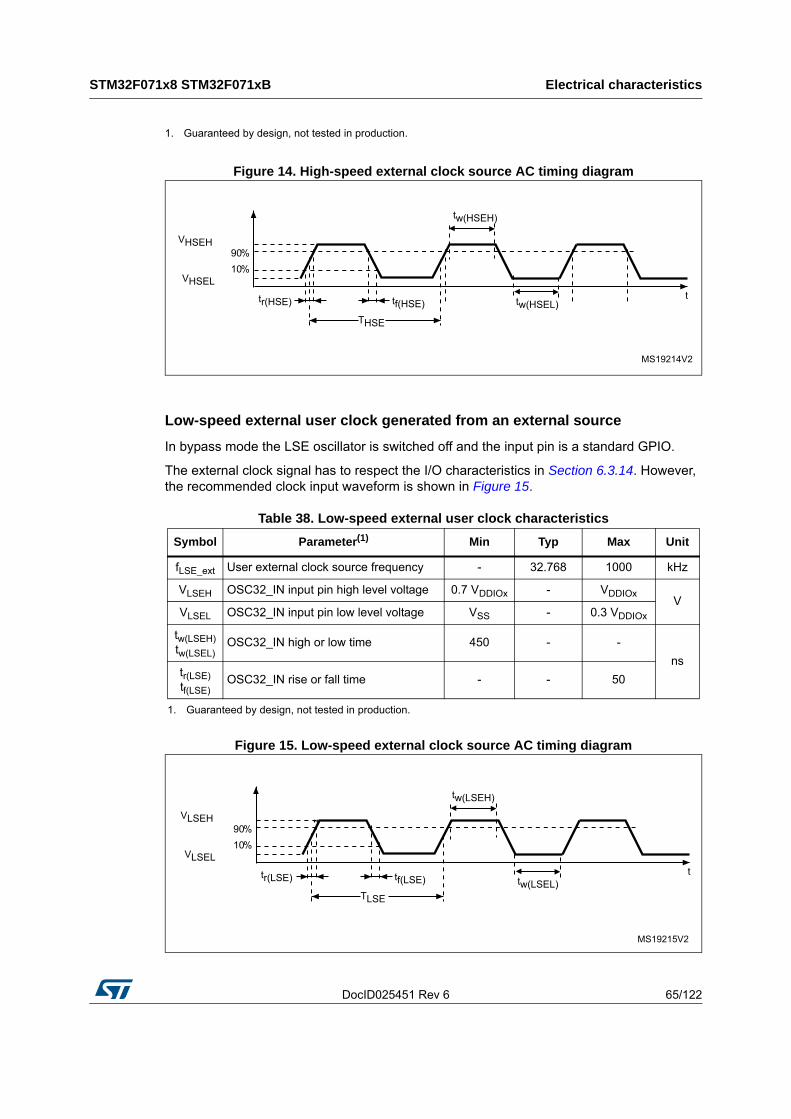
DocID025451 Rev 6 65/122
STM32F071x8 STM32F071xB Electrical characteristics
96
Figure 14. High-speed external clock source AC timing diagram
Low-speed external user clock generated from an external source
In bypass mode the LSE oscillator is switched off and the input pin is a standard GPIO.
The external clock signal has to respect the I/O characteristics in Section 6.3.14. However, the recommended clock input waveform is shown in Figure 15.
Figure 15. Low-speed external clock source AC timing diagram
1. Guaranteed by design, not tested in production.
Table 38. Low-speed external user clock characteristics
Symbol Parameter(1)
1. Guaranteed by design, not tested in production.
Min Typ Max Unit
fLSE_ext User external clock source frequency - 32.768 1000 kHz
VLSEH OSC32_IN input pin high level voltage 0.7 VDDIOx - VDDIOxV
VLSEL OSC32_IN input pin low level voltage VSS - 0.3 VDDIOx
tw(LSEH)tw(LSEL)
OSC32_IN high or low time 450 - -
nstr(LSE)tf(LSE)
OSC32_IN rise or fall time - - 50

Electrical characteristics STM32F071x8 STM32F071xB
66/122 DocID025451 Rev 6
High-speed external clock generated from a crystal/ceramic resonator
The high-speed external (HSE) clock can be supplied with a 4 to 32 MHz crystal/ceramic resonator oscillator. All the information given in this paragraph are based on design simulation results obtained with typical external components specified in Table 39. In the application, the resonator and the load capacitors have to be placed as close as possible to the oscillator pins in order to minimize output distortion and startup stabilization time. Refer to the crystal resonator manufacturer for more details on the resonator characteristics (frequency, package, accuracy).
For CL1 and CL2, it is recommended to use high-quality external ceramic capacitors in the 5 pF to 20 pF range (Typ.), designed for high-frequency applications, and selected to match the requirements of the crystal or resonator (see Figure 16). CL1 and CL2 are usually the same size. The crystal manufacturer typically specifies a load capacitance which is the series combination of CL1 and CL2. PCB and MCU pin capacitance must be included (10 pF can be used as a rough estimate of the combined pin and board capacitance) when sizing CL1 and CL2.
Note: For information on selecting the crystal, refer to the application note AN2867 “Oscillator design guide for ST microcontrollers” available from the ST website www.st.com.
Table 39. HSE oscillator characteristics
Symbol Parameter Conditions(1)
1. Resonator characteristics given by the crystal/ceramic resonator manufacturer.
Min(2) Typ Max(2)
2. Guaranteed by design, not tested in production.
Unit
fOSC_IN Oscillator frequency - 4 8 32 MHz
RF Feedback resistor - - 200 - kΩ
IDD HSE current consumption
During startup(3)
3. This consumption level occurs during the first 2/3 of the tSU(HSE) startup time
- - 8.5
mA
VDD = 3.3 V, Rm = 30 Ω,
CL = 10 pF@8 MHz- 0.4 -
VDD = 3.3 V, Rm = 45 Ω,
CL = 10 pF@8 MHz- 0.5 -
VDD = 3.3 V, Rm = 30 Ω,
CL = 5 pF@32 MHz- 0.8 -
VDD = 3.3 V, Rm = 30 Ω,
CL = 10 pF@32 MHz- 1 -
VDD = 3.3 V, Rm = 30 Ω,
CL = 20 pF@32 MHz- 1.5 -
gm Oscillator transconductance Startup 10 - - mA/V
tSU(HSE)(4)
4. tSU(HSE) is the startup time measured from the moment it is enabled (by software) to a stabilized 8 MHz oscillation is reached. This value is measured for a standard crystal resonator and it can vary significantly with the crystal manufacturer
Startup time VDD is stabilized - 2 - ms

DocID025451 Rev 6 67/122
STM32F071x8 STM32F071xB Electrical characteristics
96
Figure 16. Typical application with an 8 MHz crystal
1. REXT value depends on the crystal characteristics.
Low-speed external clock generated from a crystal resonator
The low-speed external (LSE) clock can be supplied with a 32.768 kHz crystal resonator oscillator. All the information given in this paragraph are based on design simulation results obtained with typical external components specified in Table 40. In the application, the resonator and the load capacitors have to be placed as close as possible to the oscillator pins in order to minimize output distortion and startup stabilization time. Refer to the crystal resonator manufacturer for more details on the resonator characteristics (frequency, package, accuracy).
Table 40. LSE oscillator characteristics (fLSE = 32.768 kHz)
Symbol Parameter Conditions(1) Min(2) Typ Max(2) Unit
IDD LSE current consumption
low drive capability - 0.5 0.9
µAmedium-low drive capability - - 1
medium-high drive capability - - 1.3
high drive capability - - 1.6
gmOscillator
transconductance
low drive capability 5 - -
µA/Vmedium-low drive capability 8 - -
medium-high drive capability 15 - -
high drive capability 25 - -
tSU(LSE)(3) Startup time VDDIOx is stabilized - 2 - s
1. Refer to the note and caution paragraphs below the table, and to the application note AN2867 “Oscillator design guide for ST microcontrollers”.
2. Guaranteed by design, not tested in production.
3. tSU(LSE) is the startup time measured from the moment it is enabled (by software) to a stabilized 32.768 kHz oscillation is reached. This value is measured for a standard crystal and it can vary significantly with the crystal manufacturer

Electrical characteristics STM32F071x8 STM32F071xB
68/122 DocID025451 Rev 6
Note: For information on selecting the crystal, refer to the application note AN2867 “Oscillator design guide for ST microcontrollers” available from the ST website www.st.com.
Figure 17. Typical application with a 32.768 kHz crystal
Note: An external resistor is not required between OSC32_IN and OSC32_OUT and it is forbidden to add one.
6.3.8 Internal clock source characteristics
The parameters given in Table 41 are derived from tests performed under ambient temperature and supply voltage conditions summarized in Table 24: General operating conditions. The provided curves are characterization results, not tested in production.

DocID025451 Rev 6 69/122
STM32F071x8 STM32F071xB Electrical characteristics
96
High-speed internal (HSI) RC oscillator
Figure 18. HSI oscillator accuracy characterization results for soldered parts
Table 41. HSI oscillator characteristics(1)
1. VDDA = 3.3 V, TA = -40 to 105°C unless otherwise specified.
Symbol Parameter Conditions Min Typ Max Unit
fHSI Frequency - - 8 - MHz
TRIM HSI user trimming step - - - 1(2)
2. Guaranteed by design, not tested in production.
%
DuCy(HSI) Duty cycle - 45(2) - 55(2) %
ACCHSIAccuracy of the HSI oscillator
TA = -40 to 105°C -2.8(3)
3. Data based on characterization results, not tested in production.
- 3.8(3)
%
TA = -10 to 85°C -1.9(3) - 2.3(3)
TA = 0 to 85°C -1.9(3) - 2(3)
TA = 0 to 70°C -1.3(3) - 2(3)
TA = 0 to 55°C -1(3) - 2(3)
TA = 25°C(4)
4. Factory calibrated, parts not soldered.
-1 - 1
tsu(HSI) HSI oscillator startup time - 1(2) - 2(2) µs
IDDA(HSI)HSI oscillator power consumption
- - 80 100(2) µA

Electrical characteristics STM32F071x8 STM32F071xB
70/122 DocID025451 Rev 6
High-speed internal 14 MHz (HSI14) RC oscillator (dedicated to ADC)
Figure 19. HSI14 oscillator accuracy characterization results
Table 42. HSI14 oscillator characteristics(1)
1. VDDA = 3.3 V, TA = –40 to 105 °C unless otherwise specified.
Symbol Parameter Conditions Min Typ Max Unit
fHSI14 Frequency - - 14 - MHz
TRIM HSI14 user-trimming step - - - 1(2)
2. Guaranteed by design, not tested in production.
%
DuCy(HSI14) Duty cycle - 45(2) - 55(2) %
ACCHSI14Accuracy of the HSI14 oscillator (factory calibrated)
TA = –40 to 105 °C –4.2(3)
3. Data based on characterization results, not tested in production.
- 5.1(3) %
TA = –10 to 85 °C –3.2(3) - 3.1(3) %
TA = 0 to 70 °C –2.5(3) - 2.3(3) %
TA = 25 °C –1 - 1 %
tsu(HSI14) HSI14 oscillator startup time - 1(2) - 2(2) µs
IDDA(HSI14)HSI14 oscillator power consumption
- - 100 150(2) µA

DocID025451 Rev 6 71/122
STM32F071x8 STM32F071xB Electrical characteristics
96
High-speed internal 48 MHz (HSI48) RC oscillator
Figure 20. HSI48 oscillator accuracy characterization results
Table 43. HSI48 oscillator characteristics(1)
1. VDDA = 3.3 V, TA = –40 to 105 °C unless otherwise specified.
Symbol Parameter Conditions Min Typ Max Unit
fHSI48 Frequency - - 48 - MHz
TRIM HSI48 user-trimming step - 0.09(2) 0.14 0.2(2) %
DuCy(HSI48) Duty cycle - 45(2)
2. Guaranteed by design, not tested in production.
- 55(2) %
ACCHSI48Accuracy of the HSI48 oscillator (factory calibrated)
TA = –40 to 105 °C -4.9(3)
3. Data based on characterization results, not tested in production.
- 4.7(3) %
TA = –10 to 85 °C -4.1(3) - 3.7(3) %
TA = 0 to 70 °C -3.8(3) - 3.4(3) %
TA = 25 °C -2.8 - 2.9 %
tsu(HSI48) HSI48 oscillator startup time - - - 6(2) µs
IDDA(HSI48)HSI48 oscillator power consumption
- - 312 350(2) µA

Electrical characteristics STM32F071x8 STM32F071xB
72/122 DocID025451 Rev 6
Low-speed internal (LSI) RC oscillator
6.3.9 PLL characteristics
The parameters given in Table 45 are derived from tests performed under ambient temperature and supply voltage conditions summarized in Table 24: General operating conditions.
6.3.10 Memory characteristics
Flash memory
The characteristics are given at TA = –40 to 105 °C unless otherwise specified.
Table 44. LSI oscillator characteristics(1)
1. VDDA = 3.3 V, TA = –40 to 105 °C unless otherwise specified.
Symbol Parameter Min Typ Max Unit
fLSI Frequency 30 40 50 kHz
tsu(LSI)(2)
2. Guaranteed by design, not tested in production.
LSI oscillator startup time - - 85 µs
IDDA(LSI)(2) LSI oscillator power consumption - 0.75 1.2 µA
Table 45. PLL characteristics
Symbol ParameterValue
UnitMin Typ Max
fPLL_IN
PLL input clock(1)
1. Take care to use the appropriate multiplier factors to obtain PLL input clock values compatible with the range defined by fPLL_OUT.
1(2) 8.0 24(2) MHz
PLL input clock duty cycle 40(2) - 60(2) %
fPLL_OUT PLL multiplier output clock 16(2) - 48 MHz
tLOCK PLL lock time - - 200(2)
2. Guaranteed by design, not tested in production.
µs
JitterPLL Cycle-to-cycle jitter - - 300(2) ps
Table 46. Flash memory characteristics
Symbol Parameter Conditions Min Typ Max(1)
1. Guaranteed by design, not tested in production.
Unit
tprog 16-bit programming time TA = - 40 to +105 °C 40 53.5 60 µs
tERASE Page (2 KB) erase time TA = - 40 to +105 °C 20 - 40 ms
tME Mass erase time TA = - 40 to +105 °C 20 - 40 ms
IDD Supply current Write mode - - 10 mA
Erase mode - - 12 mA

DocID025451 Rev 6 73/122
STM32F071x8 STM32F071xB Electrical characteristics
96
6.3.11 EMC characteristics
Susceptibility tests are performed on a sample basis during device characterization.
Functional EMS (electromagnetic susceptibility)
While a simple application is executed on the device (toggling 2 LEDs through I/O ports). the device is stressed by two electromagnetic events until a failure occurs. The failure is indicated by the LEDs:
• Electrostatic discharge (ESD) (positive and negative) is applied to all device pins until a functional disturbance occurs. This test is compliant with the IEC 61000-4-2 standard.
• FTB: A Burst of Fast Transient voltage (positive and negative) is applied to VDD and VSS through a 100 pF capacitor, until a functional disturbance occurs. This test is compliant with the IEC 61000-4-4 standard.
A device reset allows normal operations to be resumed.
The test results are given in Table 48. They are based on the EMS levels and classes defined in application note AN1709.
Designing hardened software to avoid noise problems
EMC characterization and optimization are performed at component level with a typical application environment and simplified MCU software. It should be noted that good EMC performance is highly dependent on the user application and the software in particular.
Therefore it is recommended that the user applies EMC software optimization and prequalification tests in relation with the EMC level requested for his application.
Table 47. Flash memory endurance and data retention
Symbol Parameter Conditions Min(1)
1. Data based on characterization results, not tested in production.
Unit
NEND Endurance TA = –40 to +105 °C 10 kcycle
tRET Data retention
1 kcycle(2) at TA = 85 °C
2. Cycling performed over the whole temperature range.
30
Year1 kcycle(2) at TA = 105 °C 10
10 kcycle(2) at TA = 55 °C 20
Table 48. EMS characteristics
Symbol Parameter ConditionsLevel/Class
VFESDVoltage limits to be applied on any I/O pin to induce a functional disturbance
VDD = 3.3 V, LQFP100, TA = +25 °C, fHCLK = 48 MHz, conforming to IEC 61000-4-2
2B
VEFTB
Fast transient voltage burst limits to be applied through 100 pF on VDD and VSS pins to induce a functional disturbance
VDD = 3.3 V, LQFP100, TA = +25°C, fHCLK = 48 MHz, conforming to IEC 61000-4-4
4B

Electrical characteristics STM32F071x8 STM32F071xB
74/122 DocID025451 Rev 6
Software recommendations
The software flowchart must include the management of runaway conditions such as:
• Corrupted program counter
• Unexpected reset
• Critical Data corruption (for example control registers)
Prequalification trials
Most of the common failures (unexpected reset and program counter corruption) can be reproduced by manually forcing a low state on the NRST pin or the Oscillator pins for 1 second.
To complete these trials, ESD stress can be applied directly on the device, over the range of specification values. When unexpected behavior is detected, the software can be hardened to prevent unrecoverable errors occurring (see application note AN1015).
Electromagnetic Interference (EMI)
The electromagnetic field emitted by the device are monitored while a simple application is executed (toggling 2 LEDs through the I/O ports). This emission test is compliant with IEC 61967-2 standard which specifies the test board and the pin loading.
6.3.12 Electrical sensitivity characteristics
Based on three different tests (ESD, LU) using specific measurement methods, the device is stressed in order to determine its performance in terms of electrical sensitivity.
Electrostatic discharge (ESD)
Electrostatic discharges (a positive then a negative pulse separated by 1 second) are applied to the pins of each sample according to each pin combination. The sample size depends on the number of supply pins in the device (3 parts × (n+1) supply pins). This test conforms to the JESD22-A114/C101 standard.
Table 49. EMI characteristics
Symbol Parameter ConditionsMonitored
frequency band
Max vs. [fHSE/fHCLK]Unit
8/48 MHz
SEMI Peak level
VDD = 3.6 V, TA = 25 °C, LQFP100 package compliant with IEC 61967-2
0.1 to 30 MHz -2
dBµV30 to 130 MHz 27
130 MHz to 1 GHz 17
EMI Level 4 -

DocID025451 Rev 6 75/122
STM32F071x8 STM32F071xB Electrical characteristics
96
Static latch-up
Two complementary static tests are required on six parts to assess the latch-up performance:
• A supply overvoltage is applied to each power supply pin.
• A current injection is applied to each input, output and configurable I/O pin.
These tests are compliant with EIA/JESD 78A IC latch-up standard.
6.3.13 I/O current injection characteristics
As a general rule, current injection to the I/O pins, due to external voltage below VSS or above VDDIOx (for standard, 3.3 V-capable I/O pins) should be avoided during normal product operation. However, in order to give an indication of the robustness of the microcontroller in cases when abnormal injection accidentally happens, susceptibility tests are performed on a sample basis during device characterization.
Functional susceptibility to I/O current injection
While a simple application is executed on the device, the device is stressed by injecting current into the I/O pins programmed in floating input mode. While current is injected into the I/O pin, one at a time, the device is checked for functional failures.
The failure is indicated by an out of range parameter: ADC error above a certain limit (higher than 5 LSB TUE), out of conventional limits of induced leakage current on adjacent pins (out of the -5 µA/+0 µA range) or other functional failure (for example reset occurrence or oscillator frequency deviation).
The characterization results are given in Table 52.
Negative induced leakage current is caused by negative injection and positive induced leakage current is caused by positive injection.
Table 50. ESD absolute maximum ratings
Symbol Ratings Conditions Packages ClassMaximum value(1) Unit
VESD(HBM)Electrostatic discharge voltage (human body model)
TA = +25 °C, conforming to JESD22-A114
All 2 2000 V
VESD(CDM)Electrostatic discharge voltage (charge device model)
TA = +25 °C, conforming to ANSI/ESD STM5.3.1
WLCSP49 C3 250V
All others C4 500
1. Data based on characterization results, not tested in production.
Table 51. Electrical sensitivities
Symbol Parameter Conditions Class
LU Static latch-up class TA = +105 °C conforming to JESD78A II level A

Electrical characteristics STM32F071x8 STM32F071xB
76/122 DocID025451 Rev 6
6.3.14 I/O port characteristics
General input/output characteristics
Unless otherwise specified, the parameters given in Table 53 are derived from tests performed under the conditions summarized in Table 24: General operating conditions. All I/Os are designed as CMOS- and TTL-compliant (except BOOT0).
Table 52. I/O current injection susceptibility
Symbol Description
Functional susceptibility
UnitNegative injection
Positive injection
IINJ
Injected current on BOOT0 and PF1 pins –0 NA
mA
Injected current on PC0 pin –0 +5
Injected current on PA11 and PA12 pins with induced leakage current on adjacent pins less than -1 mA
–5 NA
Injected current on all other FT and FTf pins –5 NA
Injected current on all other TTa, TC and RST pins –5 +5
Table 53. I/O static characteristics
Symbol Parameter Conditions Min Typ Max Unit
VILLow level input voltage
TC and TTa I/O - - 0.3 VDDIOx+0.07(1)
V
FT and FTf I/O - - 0.475 VDDIOx–0.2(1)
BOOT0 - - 0.3 VDDIOx–0.3(1)
All I/Os except BOOT0 pin
- - 0.3 VDDIOx
VIHHigh level input voltage
TC and TTa I/O 0.445 VDDIOx+0.398(1) - -
V
FT and FTf I/O 0.5 VDDIOx+0.2(1) - -
BOOT0 0.2 VDDIOx+0.95(1) - -
All I/Os except BOOT0 pin
0.7 VDDIOx - -
VhysSchmitt trigger hysteresis
TC and TTa I/O - 200(1) -
mVFT and FTf I/O - 100(1) -
BOOT0 - 300(1) -

DocID025451 Rev 6 77/122
STM32F071x8 STM32F071xB Electrical characteristics
96
All I/Os are CMOS- and TTL-compliant (no software configuration required). Their characteristics cover more than the strict CMOS-technology or TTL parameters. The coverage of these requirements is shown in Figure 21 for standard I/Os, and in Figure 22 for 5 V-tolerant I/Os. The following curves are design simulation results, not tested in production.
IlkgInput leakage current(2)
TC, FT and FTf I/O TTa in digital mode VSS ≤ VIN ≤ VDDIOx
- - ± 0.1
µA
TTa in digital mode VDDIOx ≤ VIN ≤ VDDA
- - 1
TTa in analog mode VSS ≤ VIN ≤ VDDA
- - ± 0.2
FT and FTf I/O VDDIOx ≤ VIN ≤ 5 V
- - 10
RPU
Weak pull-up equivalent resistor (3)
VIN = VSS 25 40 55 kΩ
RPD
Weak pull-down equivalent resistor(3)
VIN = - VDDIOx 25 40 55 kΩ
CIO I/O pin capacitance - - 5 - pF
1. Data based on design simulation only. Not tested in production.
2. The leakage could be higher than the maximum value, if negative current is injected on adjacent pins. Refer to Table 52: I/O current injection susceptibility.
3. Pull-up and pull-down resistors are designed with a true resistance in series with a switchable PMOS/NMOS. This PMOS/NMOS contribution to the series resistance is minimal (~10% order).
Table 53. I/O static characteristics (continued)
Symbol Parameter Conditions Min Typ Max Unit

Electrical characteristics STM32F071x8 STM32F071xB
78/122 DocID025451 Rev 6
Figure 21. TC and TTa I/O input characteristics
Figure 22. Five volt tolerant (FT and FTf) I/O input characteristics

DocID025451 Rev 6 79/122
STM32F071x8 STM32F071xB Electrical characteristics
96
Output driving current
The GPIOs (general purpose input/outputs) can sink or source up to +/-8 mA, and sink or source up to +/- 20 mA (with a relaxed VOL/VOH).
In the user application, the number of I/O pins which can drive current must be limited to respect the absolute maximum rating specified in Section 6.2:
• The sum of the currents sourced by all the I/Os on VDDIOx, plus the maximum consumption of the MCU sourced on VDD, cannot exceed the absolute maximum rating ΣIVDD (see Table 21: Voltage characteristics).
• The sum of the currents sunk by all the I/Os on VSS, plus the maximum consumption of the MCU sunk on VSS, cannot exceed the absolute maximum rating ΣIVSS (see Table 21: Voltage characteristics).
Output voltage levels
Unless otherwise specified, the parameters given in the table below are derived from tests performed under the ambient temperature and supply voltage conditions summarized in Table 24: General operating conditions. All I/Os are CMOS- and TTL-compliant (FT, TTa or TC unless otherwise specified).
Table 54. Output voltage characteristics(1)
Symbol Parameter Conditions Min Max Unit
VOL Output low level voltage for an I/O pin CMOS port(2)
|IIO| = 8 mAVDDIOx ≥ 2.7 V
- 0.4V
VOH Output high level voltage for an I/O pin VDDIOx–0.4 -
VOL Output low level voltage for an I/O pin TTL port(2)
|IIO| = 8 mAVDDIOx ≥ 2.7 V
- 0.4V
VOH Output high level voltage for an I/O pin 2.4 -
VOL(3) Output low level voltage for an I/O pin |IIO| = 20 mA
VDDIOx ≥ 2.7 V
- 1.3V
VOH(3) Output high level voltage for an I/O pin VDDIOx–1.3 -
VOL(3) Output low level voltage for an I/O pin |IIO| = 6 mA
VDDIOx ≥ 2 V
- 0.4V
VOH(3) Output high level voltage for an I/O pin VDDIOx–0.4 -
VOL(4) Output low level voltage for an I/O pin
|IIO| = 4 mA- 0.4 V
VOH(4) Output high level voltage for an I/O pin VDDIOx–0.4 - V
VOLFm+(3) Output low level voltage for an FTf I/O pin in
Fm+ mode
|IIO| = 20 mAVDDIOx ≥ 2.7 V
- 0.4 V
|IIO| = 10 mA - 0.4 V
1. The IIO current sourced or sunk by the device must always respect the absolute maximum rating specified in Table 21: Voltage characteristics, and the sum of the currents sourced or sunk by all the I/Os (I/O ports and control pins) must always respect the absolute maximum ratings ΣIIO.
2. TTL and CMOS outputs are compatible with JEDEC standards JESD36 and JESD52.
3. Data based on characterization results. Not tested in production.
4. Data based on characterization results. Not tested in production.

Electrical characteristics STM32F071x8 STM32F071xB
80/122 DocID025451 Rev 6
Input/output AC characteristics
The definition and values of input/output AC characteristics are given in Figure 23 and Table 55, respectively. Unless otherwise specified, the parameters given are derived from tests performed under the ambient temperature and supply voltage conditions summarized in Table 24: General operating conditions.
Table 55. I/O AC characteristics(1)(2)
OSPEEDRy[1:0] value(1) Symbol Parameter Conditions Min Max Unit
x0
fmax(IO)out Maximum frequency(3)
CL = 50 pF, VDDIOx ≥ 2 V
- 2 MHz
tf(IO)out Output fall time - 125ns
tr(IO)out Output rise time - 125
fmax(IO)out Maximum frequency(3)
CL = 50 pF, VDDIOx < 2 V
- 1 MHz
tf(IO)out Output fall time - 125ns
tr(IO)out Output rise time - 125
01
fmax(IO)out Maximum frequency(3)
CL = 50 pF, VDDIOx ≥ 2 V
- 10 MHz
tf(IO)out Output fall time - 25ns
tr(IO)out Output rise time - 25
fmax(IO)out Maximum frequency(3)
CL = 50 pF, VDDIOx < 2 V
- 4 MHz
tf(IO)out Output fall time - 62.5ns
tr(IO)out Output rise time - 62.5
11
fmax(IO)out Maximum frequency(3)
CL = 30 pF, VDDIOx ≥ 2.7 V - 50
MHzCL = 50 pF, VDDIOx ≥ 2.7 V - 30
CL = 50 pF, 2 V ≤ VDDIOx < 2.7 V - 20
CL = 50 pF, VDDIOx < 2 V - 10
tf(IO)out Output fall time
CL = 30 pF, VDDIOx ≥ 2.7 V - 5
ns
CL = 50 pF, VDDIOx ≥ 2.7 V - 8
CL = 50 pF, 2 V ≤ VDDIOx < 2.7 V - 12
CL = 50 pF, VDDIOx < 2 V - 25
tr(IO)out Output rise time
CL = 30 pF, VDDIOx ≥ 2.7 V - 5
CL = 50 pF, VDDIOx ≥ 2.7 V - 8
CL = 50 pF, 2 V ≤ VDDIOx < 2.7 V - 12
CL = 50 pF, VDDIOx < 2 V - 25

DocID025451 Rev 6 81/122
STM32F071x8 STM32F071xB Electrical characteristics
96
Figure 23. I/O AC characteristics definition
6.3.15 NRST pin characteristics
The NRST pin input driver uses the CMOS technology. It is connected to a permanent pull-up resistor, RPU.
Unless otherwise specified, the parameters given in the table below are derived from tests performed under the ambient temperature and supply voltage conditions summarized in Table 24: General operating conditions.
Fm+ configuration
(4)
fmax(IO)out Maximum frequency(3)
CL = 50 pF, VDDIOx ≥ 2 V
- 2 MHz
tf(IO)out Output fall time - 12ns
tr(IO)out Output rise time - 34
fmax(IO)out Maximum frequency(3)
CL = 50 pF, VDDIOx < 2 V
- 0.5 MHz
tf(IO)out Output fall time - 16ns
tr(IO)out Output rise time - 44
- tEXTIpw
Pulse width of external signals detected by the EXTI controller
- 10 - ns
1. The I/O speed is configured using the OSPEEDRx[1:0] bits. Refer to the STM32F0xxxx RM0091 reference manual for a description of GPIO Port configuration register.
2. Guaranteed by design, not tested in production.
3. The maximum frequency is defined in Figure 23.
4. When Fm+ configuration is set, the I/O speed control is bypassed. Refer to the STM32F0xxxx reference manual RM0091 for a detailed description of Fm+ I/O configuration.
Table 55. I/O AC characteristics(1)(2) (continued)
OSPEEDRy[1:0] value(1) Symbol Parameter Conditions Min Max Unit
Table 56. NRST pin characteristics
Symbol Parameter Conditions Min Typ Max Unit
VIL(NRST) NRST input low level voltage - - - 0.3 VDD+0.07(1)
VVIH(NRST) NRST input high level voltage - 0.445 VDD+0.398(1) - -

Electrical characteristics STM32F071x8 STM32F071xB
82/122 DocID025451 Rev 6
Figure 24. Recommended NRST pin protection
1. The external capacitor protects the device against parasitic resets.
2. The user must ensure that the level on the NRST pin can go below the VIL(NRST) max level specified in Table 56: NRST pin characteristics. Otherwise the reset will not be taken into account by the device.
6.3.16 12-bit ADC characteristics
Unless otherwise specified, the parameters given in Table 57 are derived from tests performed under the conditions summarized in Table 24: General operating conditions.
Note: It is recommended to perform a calibration after each power-up.
Vhys(NRST)NRST Schmitt trigger voltage hysteresis
- - 200 - mV
RPUWeak pull-up equivalent resistor(2) VIN = VSS 25 40 55 kΩ
VF(NRST) NRST input filtered pulse - - - 100(1) ns
VNF(NRST) NRST input not filtered pulse2.7 < VDD < 3.6 300(3) - -
ns2.0 < VDD < 3.6 500(3) - -
1. Data based on design simulation only. Not tested in production.
2. The pull-up is designed with a true resistance in series with a switchable PMOS. This PMOS contribution to the series resistance is minimal (~10% order).
3. Data based on design simulation only. Not tested in production.
Table 56. NRST pin characteristics (continued)
Symbol Parameter Conditions Min Typ Max Unit
Table 57. ADC characteristics
Symbol Parameter Conditions Min Typ Max Unit
VDDAAnalog supply voltage for ADC ON
- 2.4 - 3.6 V
IDDA (ADC)Current consumption of the ADC(1) VDDA = 3.3 V - 0.9 - mA
fADC ADC clock frequency - 0.6 - 14 MHz
fS(2) Sampling rate 12-bit resolution 0.043 - 1 MHz

DocID025451 Rev 6 83/122
STM32F071x8 STM32F071xB Electrical characteristics
96
fTRIG(2) External trigger frequency
fADC = 14 MHz, 12-bit resolution
- - 823 kHz
12-bit resolution - - 17 1/fADC
VAIN Conversion voltage range - 0 - VDDA V
RAIN(2) External input impedance
See Equation 1 and Table 58 for details
- - 50 kΩ
RADC(2) Sampling switch
resistance- - - 1 kΩ
CADC(2) Internal sample and hold
capacitor- - - 8 pF
tCAL(2)(3) Calibration time
fADC = 14 MHz 5.9 µs
- 83 1/fADC
WLATENCY(2)(4) ADC_DR register ready
latency
ADC clock = HSI141.5 ADC
cycles + 2 fPCLK cycles
-1.5 ADC
cycles + 3 fPCLK cycles
-
ADC clock = PCLK/2 - 4.5 -fPCLKcycle
ADC clock = PCLK/4 - 8.5 -fPCLKcycle
tlatr(2) Trigger conversion latency
fADC = fPCLK/2 = 14 MHz 0.196 µs
fADC = fPCLK/2 5.5 1/fPCLK
fADC = fPCLK/4 = 12 MHz 0.219 µs
fADC = fPCLK/4 10.5 1/fPCLK
fADC = fHSI14 = 14 MHz 0.179 - 0.250 µs
JitterADCADC jitter on trigger conversion
fADC = fHSI14 - 1 - 1/fHSI14
tS(2) Sampling time
fADC = 14 MHz 0.107 - 17.1 µs
- 1.5 - 239.5 1/fADC
tSTAB(2) Stabilization time - 14 1/fADC
tCONV(2) Total conversion time
(including sampling time)
fADC = 14 MHz, 12-bit resolution
1 - 18 µs
12-bit resolution14 to 252 (tS for sampling +12.5 for successive approximation)
1/fADC
1. During conversion of the sampled value (12.5 x ADC clock period), an additional consumption of 100 µA on IDDA and 60 µA on IDD should be taken into account.
2. Guaranteed by design, not tested in production.
3. Specified value includes only ADC timing. It does not include the latency of the register access.
4. This parameter specify latency for transfer of the conversion result to the ADC_DR register. EOC flag is set at this time.
Table 57. ADC characteristics (continued)
Symbol Parameter Conditions Min Typ Max Unit

Electrical characteristics STM32F071x8 STM32F071xB
84/122 DocID025451 Rev 6
Equation 1: RAIN max formula
The formula above (Equation 1) is used to determine the maximum external impedance allowed for an error below 1/4 of LSB. Here N = 12 (from 12-bit resolution).
RAIN
TS
fADC CADC 2N 2+( )ln××
---------------------------------------------------------------- RADC–<
Table 58. RAIN max for fADC = 14 MHz
Ts (cycles) tS (µs) RAIN max (kΩ)(1)
1.5 0.11 0.4
7.5 0.54 5.9
13.5 0.96 11.4
28.5 2.04 25.2
41.5 2.96 37.2
55.5 3.96 50
71.5 5.11 NA
239.5 17.1 NA
1. Guaranteed by design, not tested in production.
Table 59. ADC accuracy(1)(2)(3)
Symbol Parameter Test conditions Typ Max(4) Unit
ET Total unadjusted error
fPCLK = 48 MHz, fADC = 14 MHz, RAIN < 10 kΩ
VDDA = 3 V to 3.6 V
TA = 25 °C
±1.3 ±2
LSB
EO Offset error ±1 ±1.5
EG Gain error ±0.5 ±1.5
ED Differential linearity error ±0.7 ±1
EL Integral linearity error ±0.8 ±1.5
ET Total unadjusted error
fPCLK = 48 MHz, fADC = 14 MHz, RAIN < 10 kΩ
VDDA = 2.7 V to 3.6 V
TA = - 40 to 105 °C
±3.3 ±4
LSB
EO Offset error ±1.9 ±2.8
EG Gain error ±2.8 ±3
ED Differential linearity error ±0.7 ±1.3
EL Integral linearity error ±1.2 ±1.7
ET Total unadjusted error
fPCLK = 48 MHz, fADC = 14 MHz, RAIN < 10 kΩ
VDDA = 2.4 V to 3.6 V
TA = 25 °C
±3.3 ±4
LSB
EO Offset error ±1.9 ±2.8
EG Gain error ±2.8 ±3
ED Differential linearity error ±0.7 ±1.3
EL Integral linearity error ±1.2 ±1.7
1. ADC DC accuracy values are measured after internal calibration.

DocID025451 Rev 6 85/122
STM32F071x8 STM32F071xB Electrical characteristics
96
Figure 25. ADC accuracy characteristics
Figure 26. Typical connection diagram using the ADC
1. Refer to Table 57: ADC characteristics for the values of RAIN, RADC and CADC.
2. Cparasitic represents the capacitance of the PCB (dependent on soldering and PCB layout quality) plus the pad capacitance (roughly 7 pF). A high Cparasitic value will downgrade conversion accuracy. To remedy this, fADC should be reduced.
General PCB design guidelines
Power supply decoupling should be performed as shown in Figure 12: Power supply scheme. The 10 nF capacitor should be ceramic (good quality) and it should be placed as close as possible to the chip.
2. ADC Accuracy vs. Negative Injection Current: Injecting negative current on any of the standard (non-robust) analog input pins should be avoided as this significantly reduces the accuracy of the conversion being performed on another analog input. It is recommended to add a Schottky diode (pin to ground) to standard analog pins which may potentially inject negative current. Any positive injection current within the limits specified for IINJ(PIN) and ΣIINJ(PIN) in Section 6.3.14 does not affect the ADC accuracy.
3. Better performance may be achieved in restricted VDDA, frequency and temperature ranges.
4. Data based on characterization results, not tested in production.

Electrical characteristics STM32F071x8 STM32F071xB
86/122 DocID025451 Rev 6
6.3.17 DAC electrical specifications
Table 60. DAC characteristics
Symbol Parameter Min Typ Max Unit Comments
VDDAAnalog supply voltage for DAC ON
2.4 - 3.6 V -
RLOAD(1) Resistive load with buffer
ON
5 - - kΩ Load connected to VSSA
25 - - kΩ Load connected to VDDA
RO(1) Impedance output with
buffer OFF- - 15 kΩ
When the buffer is OFF, the Minimum resistive load between DAC_OUT and VSS to have a 1% accuracy is 1.5 MΩ
CLOAD(1) Capacitive load - - 50 pF
Maximum capacitive load at DAC_OUT pin (when the buffer is ON).
DAC_OUT min(1)
Lower DAC_OUT voltage with buffer ON
0.2 - - V
It gives the maximum output excursion of the DAC.
It corresponds to 12-bit input code (0x0E0) to (0xF1C) at VDDA = 3.6 V and (0x155) and (0xEAB) at VDDA = 2.4 V
DAC_OUT max(1)
Higher DAC_OUT voltage with buffer ON
- - VDDA – 0.2 V
DAC_OUT min(1)
Lower DAC_OUT voltage with buffer OFF
- 0.5 - mVIt gives the maximum output excursion of the DAC.DAC_OUT
max(1)Higher DAC_OUT voltage with buffer OFF
- - VDDA – 1LSB V
IDDA(1)
DAC DC current consumption in quiescent mode(2)
- - 600 µAWith no load, middle code (0x800) on the input
- - 700 µAWith no load, worst code (0xF1C) on the input
DNL(3)Differential non linearity Difference between two consecutive code-1LSB)
- - ±0.5 LSBGiven for the DAC in 10-bit configuration
- - ±2 LSBGiven for the DAC in 12-bit configuration
INL(3)
Integral non linearity (difference between measured value at Code i and the value at Code i on a line drawn between Code 0 and last Code 1023)
- - ±1 LSBGiven for the DAC in 10-bit configuration
- - ±4 LSBGiven for the DAC in 12-bit configuration
Offset(3)
Offset error
(difference between measured value at Code (0x800) and the ideal value = VDDA/2)
- - ±10 mV -
- - ±3 LSBGiven for the DAC in 10-bit at VDDA = 3.6 V
- - ±12 LSBGiven for the DAC in 12-bit at VDDA = 3.6 V

DocID025451 Rev 6 87/122
STM32F071x8 STM32F071xB Electrical characteristics
96
Figure 27. 12-bit buffered / non-buffered DAC
1. The DAC integrates an output buffer that can be used to reduce the output impedance and to drive external loads directly without the use of an external operational amplifier. The buffer can be bypassed by configuring the BOFFx bit in the DAC_CR register.
Gain error(3) Gain error - - ±0.5 %Given for the DAC in 12-bit configuration
tSETTLING(3)
Settling time (full scale: for a 10-bit input code transition between the lowest and the highest input codes when DAC_OUT reaches final value ±1LSB
- 3 4 µs CLOAD ≤ 50 pF, RLOAD ≥ 5 kΩ
Update rate(3)
Max frequency for a correct DAC_OUT change when small variation in the input code (from code i to i+1LSB)
- - 1 MS/s CLOAD ≤ 50 pF, RLOAD ≥ 5 kΩ
tWAKEUP(3)
Wakeup time from off state (Setting the ENx bit in the DAC Control register)
- 6.5 10 µsCLOAD ≤ 50 pF, RLOAD ≥ 5 kΩ input code between lowest and highest possible ones.
PSRR+ (1)Power supply rejection ratio (to VDDA) (static DC measurement
- –67 –40 dB No RLOAD, CLOAD = 50 pF
1. Guaranteed by design, not tested in production.
2. The DAC is in “quiescent mode” when it keeps the value steady on the output so no dynamic consumption is involved.
3. Data based on characterization results, not tested in production.
Table 60. DAC characteristics (continued)
Symbol Parameter Min Typ Max Unit Comments

Electrical characteristics STM32F071x8 STM32F071xB
88/122 DocID025451 Rev 6
6.3.18 Comparator characteristics
Table 61. Comparator characteristics
Symbol Parameter Conditions Min(1) Typ Max(1) Unit
VDDA Analog supply voltage - VDD - 3.6 V
VINComparator input voltage range
- 0 - VDDA -
VSCVREFINT scaler offset voltage
- - ±5 ±10 mV
tS_SCVREFINT scaler startup time from power down
First VREFINT scaler activation after device power on
- -1000
(2)ms
Next activations - - 0.2
tSTARTComparator startup time
Startup time to reach propagation delay specification
- - 60 µs
tD
Propagation delay for 200 mV step with 100 mV overdrive
Ultra-low power mode - 2 4.5
µsLow power mode - 0.7 1.5
Medium power mode - 0.3 0.6
High speed modeVDDA ≥ 2.7 V - 50 100
nsVDDA < 2.7 V - 100 240
Propagation delay for full range step with 100 mV overdrive
Ultra-low power mode - 2 7
µsLow power mode - 0.7 2.1
Medium power mode - 0.3 1.2
High speed modeVDDA ≥ 2.7 V - 90 180
nsVDDA < 2.7 V - 110 300
Voffset Comparator offset error - - ±4 ±10 mV
dVoffset/dTOffset error temperature coefficient
- - 18 - µV/°C
IDD(COMP)COMP current consumption
Ultra-low power mode - 1.2 1.5
µALow power mode - 3 5
Medium power mode - 10 15
High speed mode - 75 100

DocID025451 Rev 6 89/122
STM32F071x8 STM32F071xB Electrical characteristics
96
Figure 28. Maximum VREFINT scaler startup time from power down
Vhys Comparator hysteresis
No hysteresis (COMPxHYST[1:0]=00)
- - 0 -
mV
Low hysteresis (COMPxHYST[1:0]=01)
High speed mode 3
8
13
All other power modes
5 10
Medium hysteresis (COMPxHYST[1:0]=10)
High speed mode 7
15
26
All other power modes
9 19
High hysteresis (COMPxHYST[1:0]=11)
High speed mode 18
31
49
All other power modes
19 40
1. Data based on characterization results, not tested in production.
2. For more details and conditions see Figure 28: Maximum VREFINT scaler startup time from power down.
Table 61. Comparator characteristics (continued)
Symbol Parameter Conditions Min(1) Typ Max(1) Unit
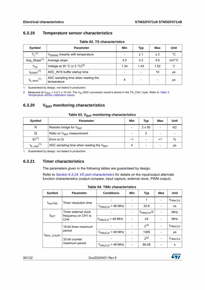
Electrical characteristics STM32F071x8 STM32F071xB
90/122 DocID025451 Rev 6
6.3.19 Temperature sensor characteristics
6.3.20 VBAT monitoring characteristics
6.3.21 Timer characteristics
The parameters given in the following tables are guaranteed by design.
Refer to Section 6.3.14: I/O port characteristics for details on the input/output alternate function characteristics (output compare, input capture, external clock, PWM output).
Table 62. TS characteristics
Symbol Parameter Min Typ Max Unit
TL(1) VSENSE linearity with temperature - ± 1 ± 2 °C
Avg_Slope(1) Average slope 4.0 4.3 4.6 mV/°C
V30 Voltage at 30 °C (± 5 °C)(2) 1.34 1.43 1.52 V
tSTART(1) ADC_IN16 buffer startup time - - 10 µs
tS_temp(1) ADC sampling time when reading the
temperature4 - - µs
1. Guaranteed by design, not tested in production.
2. Measured at VDDA = 3.3 V ± 10 mV. The V30 ADC conversion result is stored in the TS_CAL1 byte. Refer to Table 3: Temperature sensor calibration values.
Table 63. VBAT monitoring characteristics
Symbol Parameter Min Typ Max Unit
R Resistor bridge for VBAT - 2 x 50 - kΩ
Q Ratio on VBAT measurement - 2 - -
Er(1) Error on Q –1 - +1 %
tS_vbat(1) ADC sampling time when reading the VBAT 4 - - µs
1. Guaranteed by design, not tested in production.
Table 64. TIMx characteristics
Symbol Parameter Conditions Min Typ Max Unit
tres(TIM) Timer resolution time- - 1 - tTIMxCLK
fTIMxCLK = 48 MHz - 20.8 - ns
fEXT
Timer external clock frequency on CH1 to CH4
- - fTIMxCLK/2 - MHz
fTIMxCLK = 48 MHz - 24 - MHz
tMAX_COUNT
16-bit timer maximum period
- - 216 - tTIMxCLK
fTIMxCLK = 48 MHz - 1365 - µs
32-bit counter maximum period
- - 232 - tTIMxCLK
fTIMxCLK = 48 MHz - 89.48 - s
DocID025451 Rev 6 91/122
STM32F071x8 STM32F071xB Electrical characteristics
96
6.3.22 Communication interfaces
I2C interface characteristics
The I2C interface meets the timings requirements of the I2C-bus specification and user manual rev. 03 for:
• Standard-mode (Sm): with a bit rate up to 100 kbit/s
• Fast-mode (Fm): with a bit rate up to 400 kbit/s
• Fast-mode Plus (Fm+): with a bit rate up to 1 Mbit/s.
The I2C timings requirements are guaranteed by design when the I2Cx peripheral is properly configured (refer to Reference manual).
The SDA and SCL I/O requirements are met with the following restrictions: the SDA and SCL I/O pins are not “true” open-drain. When configured as open-drain, the PMOS connected between the I/O pin and VDDIOx is disabled, but is still present. Only FTf I/O pins support Fm+ low level output current maximum requirement. Refer to Section 6.3.14: I/O port characteristics for the I2C I/Os characteristics.
All I2C SDA and SCL I/Os embed an analog filter. Refer to the table below for the analog filter characteristics:
Table 65. IWDG min/max timeout period at 40 kHz (LSI)(1)
1. These timings are given for a 40 kHz clock but the microcontroller internal RC frequency can vary from 30 to 60 kHz. Moreover, given an exact RC oscillator frequency, the exact timings still depend on the phasing of the APB interface clock versus the LSI clock so that there is always a full RC period of uncertainty.
Prescaler divider PR[2:0] bitsMin timeout RL[11:0]=
0x000Max timeout RL[11:0]=
0xFFFUnit
/4 0 0.1 409.6
ms
/8 1 0.2 819.2
/16 2 0.4 1638.4
/32 3 0.8 3276.8
/64 4 1.6 6553.6
/128 5 3.2 13107.2
/256 6 or 7 6.4 26214.4
Table 66. WWDG min/max timeout value at 48 MHz (PCLK)
Prescaler WDGTB Min timeout value Max timeout value Unit
1 0 0.0853 5.4613
ms2 1 0.1706 10.9226
4 2 0.3413 21.8453
8 3 0.6826 43.6906

Electrical characteristics STM32F071x8 STM32F071xB
92/122 DocID025451 Rev 6
SPI/I2S characteristics
Unless otherwise specified, the parameters given in Table 68 for SPI or in Table 69 for I2S are derived from tests performed under the ambient temperature, fPCLKx frequency and supply voltage conditions summarized in Table 24: General operating conditions.
Refer to Section 6.3.14: I/O port characteristics for more details on the input/output alternate function characteristics (NSS, SCK, MOSI, MISO for SPI and WS, CK, SD for I2S).
Table 67. I2C analog filter characteristics(1)
1. Guaranteed by design, not tested in production.
Symbol Parameter Min Max Unit
tAFMaximum width of spikes that are suppressed by the analog filter
50(2)
2. Spikes with widths below tAF(min) are filtered.
260(3)
3. Spikes with widths above tAF(max) are not filtered
ns
Table 68. SPI characteristics(1)
Symbol Parameter Conditions Min Max Unit
fSCK1/tc(SCK)
SPI clock frequencyMaster mode - 18
MHzSlave mode - 18
tr(SCK)tf(SCK)
SPI clock rise and fall time
Capacitive load: C = 15 pF - 6 ns
tsu(NSS) NSS setup time Slave mode 4Tpclk -
ns
th(NSS) NSS hold time Slave mode 2Tpclk + 10 -
tw(SCKH)tw(SCKL)
SCK high and low timeMaster mode, fPCLK = 36 MHz, presc = 4
Tpclk/2 -2 Tpclk/2 + 1
tsu(MI)tsu(SI)
Data input setup timeMaster mode 4 -
Slave mode 5 -
th(MI)Data input hold time
Master mode 4 -
th(SI) Slave mode 5 -
ta(SO)(2) Data output access time Slave mode, fPCLK = 20 MHz 0 3Tpclk
tdis(SO)(3) Data output disable time Slave mode 0 18
tv(SO) Data output valid time Slave mode (after enable edge) - 22.5
tv(MO) Data output valid time Master mode (after enable edge) - 6
th(SO)Data output hold time
Slave mode (after enable edge) 11.5 -
th(MO) Master mode (after enable edge) 2 -
DuCy(SCK)SPI slave input clock duty cycle
Slave mode 25 75 %
1. Data based on characterization results, not tested in production.
2. Min time is for the minimum time to drive the output and the max time is for the maximum time to validate the data.
3. Min time is for the minimum time to invalidate the output and the max time is for the maximum time to put the data in Hi-Z

DocID025451 Rev 6 93/122
STM32F071x8 STM32F071xB Electrical characteristics
96
Figure 29. SPI timing diagram - slave mode and CPHA = 0
Figure 30. SPI timing diagram - slave mode and CPHA = 1
1. Measurement points are done at CMOS levels: 0.3 VDD and 0.7 VDD.
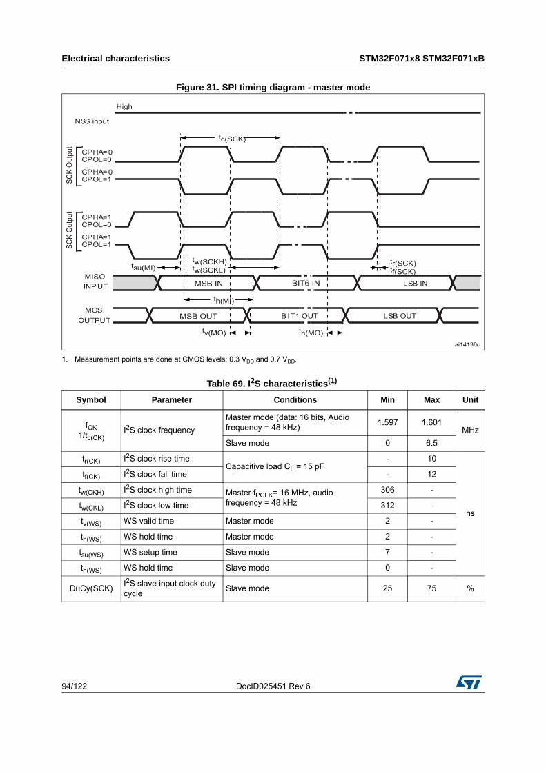
Electrical characteristics STM32F071x8 STM32F071xB
94/122 DocID025451 Rev 6
Figure 31. SPI timing diagram - master mode
1. Measurement points are done at CMOS levels: 0.3 VDD and 0.7 VDD.
Table 69. I2S characteristics(1)
Symbol Parameter Conditions Min Max Unit
fCK1/tc(CK)
I2S clock frequency
Master mode (data: 16 bits, Audio frequency = 48 kHz)
1.597 1.601MHz
Slave mode 0 6.5
tr(CK) I2S clock rise timeCapacitive load CL = 15 pF
- 10
ns
tf(CK) I2S clock fall time - 12
tw(CKH) I2S clock high time Master fPCLK= 16 MHz, audio frequency = 48 kHz
306 -
tw(CKL) I2S clock low time 312 -
tv(WS) WS valid time Master mode 2 -
th(WS) WS hold time Master mode 2 -
tsu(WS) WS setup time Slave mode 7 -
th(WS) WS hold time Slave mode 0 -
DuCy(SCK)I2S slave input clock duty cycle
Slave mode 25 75 %

DocID025451 Rev 6 95/122
STM32F071x8 STM32F071xB Electrical characteristics
96
Figure 32. I2S slave timing diagram (Philips protocol)
1. Measurement points are done at CMOS levels: 0.3 × VDDIOx and 0.7 × VDDIOx.
2. LSB transmit/receive of the previously transmitted byte. No LSB transmit/receive is sent before the first byte.
tsu(SD_MR) Data input setup time
Master receiver 6 -
ns
tsu(SD_SR) Slave receiver 2 -
th(SD_MR)(2)
Data input hold timeMaster receiver 4 -
th(SD_SR)(2) Slave receiver 0.5 -
tv(SD_MT)(2)
Data output valid timeMaster transmitter - 4
tv(SD_ST)(2) Slave transmitter - 20
th(SD_MT)Data output hold time
Master transmitter 0 -
th(SD_ST) Slave transmitter 13 -
1. Data based on design simulation and/or characterization results, not tested in production.
2. Depends on fPCLK. For example, if fPCLK = 8 MHz, then TPCLK = 1/fPLCLK = 125 ns.
Table 69. I2S characteristics(1) (continued)
Symbol Parameter Conditions Min Max Unit
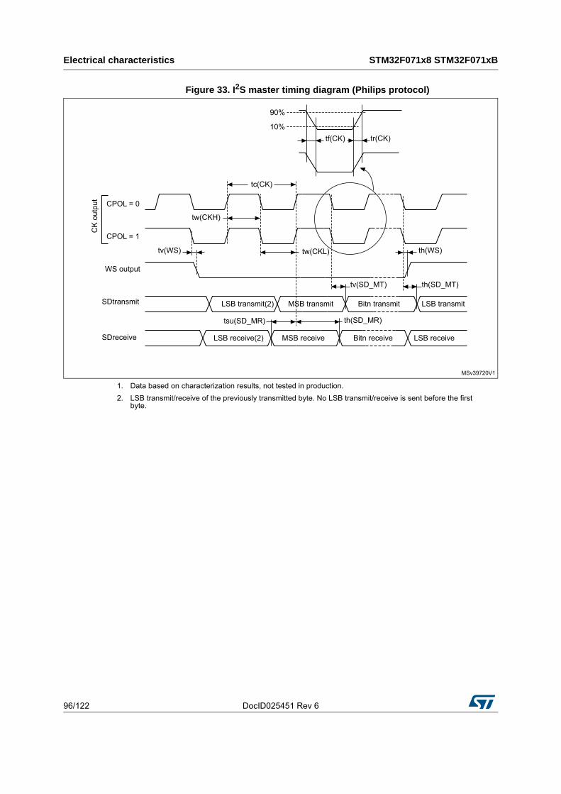
Electrical characteristics STM32F071x8 STM32F071xB
96/122 DocID025451 Rev 6
Figure 33. I2S master timing diagram (Philips protocol)
1. Data based on characterization results, not tested in production.
2. LSB transmit/receive of the previously transmitted byte. No LSB transmit/receive is sent before the first byte.

DocID025451 Rev 6 97/122
STM32F071x8 STM32F071xB Package information
118
7 Package information
In order to meet environmental requirements, ST offers these devices in different grades of ECOPACK® packages, depending on their level of environmental compliance. ECOPACK® specifications, grade definitions and product status are available at: www.st.com. ECOPACK® is an ST trademark.
7.1 UFBGA100 package information
UFBGA100 is a 100-ball, 7 x 7 mm, 0.50 mm pitch, ultra-fine-profile ball grid array package.
Figure 34. UFBGA100 package outline
1. Drawing is not to scale.
Table 70. UFBGA100 package mechanical data
Symbolmillimeters inches(1)
Min. Typ. Max. Min. Typ. Max.
A - - 0.600 - - 0.0236
A1 - - 0.110 - - 0.0043
A2 - 0.450 - - 0.0177 -
A3 - 0.130 - - 0.0051 0.0094
A4 - 0.320 - - 0.0126 -
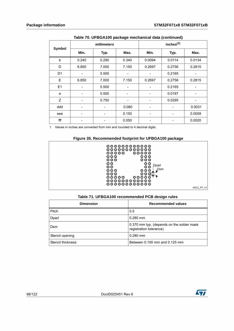
Package information STM32F071x8 STM32F071xB
98/122 DocID025451 Rev 6
Figure 35. Recommended footprint for UFBGA100 package
b 0.240 0.290 0.340 0.0094 0.0114 0.0134
D 6.850 7.000 7.150 0.2697 0.2756 0.2815
D1 - 5.500 - - 0.2165 -
E 6.850 7.000 7.150 0.2697 0.2756 0.2815
E1 - 5.500 - - 0.2165 -
e - 0.500 - - 0.0197 -
Z - 0.750 - - 0.0295 -
ddd - - 0.080 - - 0.0031
eee - - 0.150 - - 0.0059
fff - - 0.050 - - 0.0020
1. Values in inches are converted from mm and rounded to 4 decimal digits.
Table 71. UFBGA100 recommended PCB design rules
Dimension Recommended values
Pitch 0.5
Dpad 0.280 mm
Dsm0.370 mm typ. (depends on the solder mask registration tolerance)
Stencil opening 0.280 mm
Stencil thickness Between 0.100 mm and 0.125 mm
Table 70. UFBGA100 package mechanical data (continued)
Symbolmillimeters inches(1)
Min. Typ. Max. Min. Typ. Max.

DocID025451 Rev 6 99/122
STM32F071x8 STM32F071xB Package information
118
Device marking
The following figure gives an example of topside marking orientation versus pin 1 identifier location.
Other optional marking or inset/upset marks, which identify the parts throughout supply chain operations, are not indicated below.
Figure 36. UFBGA100 package marking example
1. Parts marked as "ES", "E" or accompanied by an Engineering Sample notification letter, are not yet qualified and therefore not yet ready to be used in production and any consequences deriving from such usage will not be at ST charge. In no event, ST will be liable for any customer usage of these engineering samples in production. ST Quality has to be contacted prior to any decision to use these Engineering Samples to run qualification activity.

Package information STM32F071x8 STM32F071xB
100/122 DocID025451 Rev 6
7.2 LQFP100 package information
LQFP100 is a100-pin, 14 x 14 mm low-profile quad flat package.
Figure 37. LQFP100 package outline
1. Drawing is not to scale.
Table 72. LQPF100 package mechanical data
Symbolmillimeters inches(1)
Min Typ Max Min Typ Max
A - - 1.600 - - 0.0630
A1 0.050 - 0.150 0.0020 - 0.0059
A2 1.350 1.400 1.450 0.0531 0.0551 0.0571
b 0.170 0.220 0.270 0.0067 0.0087 0.0106
c 0.090 - 0.200 0.0035 - 0.0079
D 15.800 16.000 16.200 0.6220 0.6299 0.6378
D1 13.800 14.000 14.200 0.5433 0.5512 0.5591
D3 - 12.000 - - 0.4724 -
E 15.800 16.000 16.200 0.6220 0.6299 0.6378

DocID025451 Rev 6 101/122
STM32F071x8 STM32F071xB Package information
118
Figure 38. Recommended footprint for LQFP100 package
1. Dimensions are expressed in millimeters.
E1 13.800 14.000 14.200 0.5433 0.5512 0.5591
E3 - 12.000 - - 0.4724 -
e - 0.500 - - 0.0197 -
L 0.450 0.600 0.750 0.0177 0.0236 0.0295
L1 - 1.000 - - 0.0394 -
k 0.0° 3.5° 7.0° 0.0° 3.5° 7.0°
ccc - - 0.080 - - 0.0031
1. Values in inches are converted from mm and rounded to 4 decimal digits.
Table 72. LQPF100 package mechanical data (continued)
Symbolmillimeters inches(1)
Min Typ Max Min Typ Max

Package information STM32F071x8 STM32F071xB
102/122 DocID025451 Rev 6
Device marking
The following figure gives an example of topside marking orientation versus pin 1 identifier location.
Other optional marking or inset/upset marks, which identify the parts throughout supply chain operations, are not indicated below.
Figure 39. LQFP100 package marking example
1. Parts marked as "ES", "E" or accompanied by an Engineering Sample notification letter, are not yet qualified and therefore not yet ready to be used in production and any consequences deriving from such usage will not be at ST charge. In no event, ST will be liable for any customer usage of these engineering samples in production. ST Quality has to be contacted prior to any decision to use these Engineering Samples to run qualification activity.
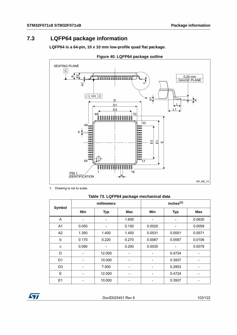
DocID025451 Rev 6 103/122
STM32F071x8 STM32F071xB Package information
118
7.3 LQFP64 package information
LQFP64 is a 64-pin, 10 x 10 mm low-profile quad flat package.
Figure 40. LQFP64 package outline
1. Drawing is not to scale.
Table 73. LQFP64 package mechanical data
Symbolmillimeters inches(1)
Min Typ Max Min Typ Max
A - - 1.600 - - 0.0630
A1 0.050 - 0.150 0.0020 - 0.0059
A2 1.350 1.400 1.450 0.0531 0.0551 0.0571
b 0.170 0.220 0.270 0.0067 0.0087 0.0106
c 0.090 - 0.200 0.0035 - 0.0079
D - 12.000 - - 0.4724 -
D1 - 10.000 - - 0.3937 -
D3 - 7.500 - - 0.2953 -
E - 12.000 - - 0.4724 -
E1 - 10.000 - - 0.3937 -
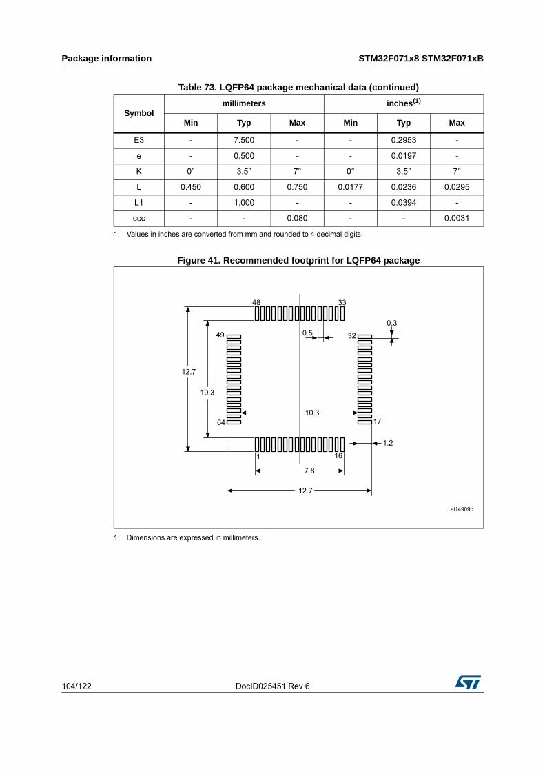
Package information STM32F071x8 STM32F071xB
104/122 DocID025451 Rev 6
Figure 41. Recommended footprint for LQFP64 package
1. Dimensions are expressed in millimeters.
E3 - 7.500 - - 0.2953 -
e - 0.500 - - 0.0197 -
K 0° 3.5° 7° 0° 3.5° 7°
L 0.450 0.600 0.750 0.0177 0.0236 0.0295
L1 - 1.000 - - 0.0394 -
ccc - - 0.080 - - 0.0031
1. Values in inches are converted from mm and rounded to 4 decimal digits.
Table 73. LQFP64 package mechanical data (continued)
Symbolmillimeters inches(1)
Min Typ Max Min Typ Max
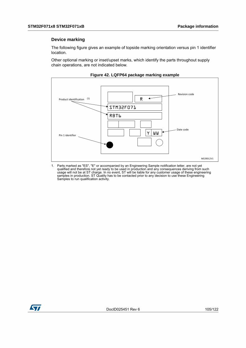
DocID025451 Rev 6 105/122
STM32F071x8 STM32F071xB Package information
118
Device marking
The following figure gives an example of topside marking orientation versus pin 1 identifier location.
Other optional marking or inset/upset marks, which identify the parts throughout supply chain operations, are not indicated below.
Figure 42. LQFP64 package marking example
1. Parts marked as "ES", "E" or accompanied by an Engineering Sample notification letter, are not yet qualified and therefore not yet ready to be used in production and any consequences deriving from such usage will not be at ST charge. In no event, ST will be liable for any customer usage of these engineering samples in production. ST Quality has to be contacted prior to any decision to use these Engineering Samples to run qualification activity.

Package information STM32F071x8 STM32F071xB
106/122 DocID025451 Rev 6
7.4 WLCSP49 package information
WLCSP49 is a 49-ball, 3.277 x 3.109 mm, 0.4 mm pitch wafer-level chip-scale package.
Figure 43. WLCSP49 package outline
1. Drawing is not to scale.

DocID025451 Rev 6 107/122
STM32F071x8 STM32F071xB Package information
118
Table 74. WLCSP49 package mechanical data
Symbolmillimeters inches(1)
1. Values in inches are converted from mm and rounded to 4 decimal digits.
Min Typ Max Min Typ Max
A 0.525 0.555 0.585 0.0207 0.0219 0.0230
A1 - 0.175 - - 0.0069 -
A2 - 0.380 - - 0.0150 -
A3(2)
2. Back side coating
- 0.025 - - 0.0010 -
b(3)
3. Dimension is measured at the maximum bump diameter parallel to primary datum Z.
0.220 0.250 0.280 0.0087 0.0098 0.0110
D 3.242 3.277 3.312 0.1276 0.1290 0.1304
E 3.074 3.109 3.144 0.1210 0.1224 0.1238
e - 0.400 - - 0.0157 -
e1 - 2.400 - - 0.0945 -
e2 - 2.400 - - 0.0945 -
F - 0.4385 - - 0.0173 -
G - 0.3545 - - 0.0140 -
aaa - - 0.100 - - 0.0039
bbb - - 0.100 - - 0.0039
ccc - - 0.100 - - 0.0039
ddd - - 0.050 - - 0.0020
eee - - 0.050 - - 0.0020

Package information STM32F071x8 STM32F071xB
108/122 DocID025451 Rev 6
Device marking
The following figure gives an example of topside marking orientation versus ball A1 identifier location.
Other optional marking or inset/upset marks, which identify the parts throughout supply chain operations, are not indicated below.
Figure 44. WLCSP49 package marking example
1. Parts marked as "ES", "E" or accompanied by an Engineering Sample notification letter, are not yet qualified and therefore not yet ready to be used in production and any consequences deriving from such usage will not be at ST charge. In no event, ST will be liable for any customer usage of these engineering samples in production. ST Quality has to be contacted prior to any decision to use these Engineering Samples to run qualification activity.

DocID025451 Rev 6 109/122
STM32F071x8 STM32F071xB Package information
118
7.5 LQFP48 package information
LQFP48 is a 48-pin, 7 x 7 mm low-profile quad flat package.
Figure 45. LQFP48 package outline
1. Drawing is not to scale.

Package information STM32F071x8 STM32F071xB
110/122 DocID025451 Rev 6
Figure 46. Recommended footprint for LQFP48 package
1. Dimensions are expressed in millimeters.
Table 75. LQFP48 package mechanical data
Symbolmillimeters inches(1)
1. Values in inches are converted from mm and rounded to 4 decimal digits.
Min Typ Max Min Typ Max
A - - 1.600 - - 0.0630
A1 0.050 - 0.150 0.0020 - 0.0059
A2 1.350 1.400 1.450 0.0531 0.0551 0.0571
b 0.170 0.220 0.270 0.0067 0.0087 0.0106
c 0.090 - 0.200 0.0035 - 0.0079
D 8.800 9.000 9.200 0.3465 0.3543 0.3622
D1 6.800 7.000 7.200 0.2677 0.2756 0.2835
D3 - 5.500 - - 0.2165 -
E 8.800 9.000 9.200 0.3465 0.3543 0.3622
E1 6.800 7.000 7.200 0.2677 0.2756 0.2835
E3 - 5.500 - - 0.2165 -
e - 0.500 - - 0.0197 -
L 0.450 0.600 0.750 0.0177 0.0236 0.0295
L1 - 1.000 - - 0.0394 -
k 0° 3.5° 7° 0° 3.5° 7°
ccc - - 0.080 - - 0.0031

DocID025451 Rev 6 111/122
STM32F071x8 STM32F071xB Package information
118
Device marking
The following figure gives an example of topside marking orientation versus pin 1 identifier location.
Other optional marking or inset/upset marks, which identify the parts throughout supply chain operations, are not indicated below.
Figure 47. LQFP48 package marking example
1. Parts marked as "ES", "E" or accompanied by an Engineering Sample notification letter, are not yet qualified and therefore not yet ready to be used in production and any consequences deriving from such usage will not be at ST charge. In no event, ST will be liable for any customer usage of these engineering samples in production. ST Quality has to be contacted prior to any decision to use these Engineering Samples to run qualification activity.

Package information STM32F071x8 STM32F071xB
112/122 DocID025451 Rev 6
7.6 UFQFPN48 package information
UFQFPN48 is a 48-lead, 7x7 mm, 0.5 mm pitch, ultra-thin fine-pitch quad flat package.
Figure 48. UFQFPN48 package outline
1. Drawing is not to scale.
2. All leads/pads should also be soldered to the PCB to improve the lead/pad solder joint life.
3. There is an exposed die pad on the underside of the UFQFPN package. It is recommended to connect and solder this back-side pad to PCB ground.
DocID025451 Rev 6 113/122
STM32F071x8 STM32F071xB Package information
118
Figure 49. Recommended footprint for UFQFPN48 package
1. Dimensions are expressed in millimeters.
Table 76. UFQFPN48 package mechanical data
Symbolmillimeters inches(1)
1. Values in inches are converted from mm and rounded to 4 decimal digits.
Min Typ Max Min Typ Max
A 0.500 0.550 0.600 0.0197 0.0217 0.0236
A1 0.000 0.020 0.050 0.0000 0.0008 0.0020
D 6.900 7.000 7.100 0.2717 0.2756 0.2795
E 6.900 7.000 7.100 0.2717 0.2756 0.2795
D2 5.500 5.600 5.700 0.2165 0.2205 0.2244
E2 5.500 5.600 5.700 0.2165 0.2205 0.2244
L 0.300 0.400 0.500 0.0118 0.0157 0.0197
T - 0.152 - - 0.0060 -
b 0.200 0.250 0.300 0.0079 0.0098 0.0118
e - 0.500 - - 0.0197 -
ddd - - 0.080 - - 0.0031

Package information STM32F071x8 STM32F071xB
114/122 DocID025451 Rev 6
Device marking
The following figure gives an example of topside marking orientation versus pin 1 identifier location.
Other optional marking or inset/upset marks, which identify the parts throughout supply chain operations, are not indicated below.
Figure 50. UFQFPN48 package marking example
1. Parts marked as "ES", "E" or accompanied by an Engineering Sample notification letter, are not yet qualified and therefore not yet ready to be used in production and any consequences deriving from such usage will not be at ST charge. In no event, ST will be liable for any customer usage of these engineering samples in production. ST Quality has to be contacted prior to any decision to use these Engineering Samples to run qualification activity.

DocID025451 Rev 6 115/122
STM32F071x8 STM32F071xB Package information
118
7.7 Thermal characteristics
The maximum chip junction temperature (TJmax) must never exceed the values given in Table 24: General operating conditions.
The maximum chip-junction temperature, TJ max, in degrees Celsius, may be calculated using the following equation:
TJ max = TA max + (PD max x ΘJA)
Where:
• TA max is the maximum ambient temperature in °C,
• ΘJA is the package junction-to-ambient thermal resistance, in °C/W,
• PD max is the sum of PINT max and PI/O max (PD max = PINT max + PI/Omax),
• PINT max is the product of IDD and VDD, expressed in Watts. This is the maximum chip internal power.
PI/O max represents the maximum power dissipation on output pins where:
PI/O max = Σ (VOL × IOL) + Σ ((VDDIOx – VOH) × IOH),
taking into account the actual VOL / IOL and VOH / IOH of the I/Os at low and high level in the application.
7.7.1 Reference document
JESD51-2 Integrated Circuits Thermal Test Method Environment Conditions - Natural Convection (Still Air). Available from www.jedec.org
7.7.2 Selecting the product temperature range
When ordering the microcontroller, the temperature range is specified in the ordering information scheme shown in Section 8: Ordering information.
Each temperature range suffix corresponds to a specific guaranteed ambient temperature at maximum dissipation and, to a specific maximum junction temperature.
Table 77. Package thermal characteristics
Symbol Parameter Value Unit
ΘJA
Thermal resistance junction-ambient UFBGA100 - 7 × 7 mm
55
°C/W
Thermal resistance junction-ambient LQFP100 - 14 × 14 mm
42
Thermal resistance junction-ambient LQFP64 - 10 × 10 mm / 0.5 mm pitch
44
Thermal resistance junction-ambient LQFP48 - 7 × 7 mm
54
Thermal resistance junction-ambient UFQFPN48 - 7 × 7 mm
32
Thermal resistance junction-ambient WLCSP49 - 0.4 mm pitch
49

Package information STM32F071x8 STM32F071xB
116/122 DocID025451 Rev 6
As applications do not commonly use the STM32F071x8/xB at maximum dissipation, it is useful to calculate the exact power consumption and junction temperature to determine which temperature range will be best suited to the application.
The following examples show how to calculate the temperature range needed for a given application.
Example 1: High-performance application
Assuming the following application conditions:
Maximum temperature TAmax = 82 °C (measured according to JESD51-2), IDDmax = 50 mA, VDD = 3.5 V, maximum 20 I/Os used at the same time in output at low level with IOL = 8 mA, VOL= 0.4 V and maximum 8 I/Os used at the same time in output at low level with IOL = 20 mA, VOL= 1.3 V
PINTmax = 50 mA × 3.5 V= 175 mW
PIOmax = 20 × 8 mA × 0.4 V + 8 × 20 mA × 1.3 V = 272 mW
This gives: PINTmax = 175 mW and PIOmax = 272 mW:
PDmax= 175 + 272 = 447 mW
Using the values obtained in Table 77 TJmax is calculated as follows:
– For LQFP64, 45 °C/W
TJmax = 82 °C + (45 °C/W × 447 mW) = 82 °C + 20.115 °C = 102.115 °C
This is within the range of the suffix 6 version parts (–40 < TJ < 105 °C).
In this case, parts must be ordered at least with the temperature range suffix 6 (see Section 8: Ordering information).
Note: With this given PDmax we can find the TAmax allowed for a given device temperature range (order code suffix 6 or 7).
Suffix 6: TAmax = TJmax - (45°C/W × 447 mW) = 105-20.115 = 84.885 °C
Suffix 7: TAmax = TJmax - (45°C/W × 447 mW) = 125-20.115 = 104.885 °C
Example 2: High-temperature application
Using the same rules, it is possible to address applications that run at high temperatures with a low dissipation, as long as junction temperature TJ remains within the specified range.
Assuming the following application conditions:
Maximum temperature TAmax = 100 °C (measured according to JESD51-2), IDDmax = 20 mA, VDD = 3.5 V, maximum 20 I/Os used at the same time in output at low level with IOL = 8 mA, VOL= 0.4 V
PINTmax = 20 mA × 3.5 V= 70 mW
PIOmax = 20 × 8 mA × 0.4 V = 64 mW
This gives: PINTmax = 70 mW and PIOmax = 64 mW:
PDmax = 70 + 64 = 134 mW
Thus: PDmax = 134 mW
Using the values obtained in Table 77 TJmax is calculated as follows:
– For LQFP64, 45 °C/W
TJmax = 100 °C + (45 °C/W × 134 mW) = 100 °C + 6.03 °C = 106.03 °C

DocID025451 Rev 6 117/122
STM32F071x8 STM32F071xB Package information
118
This is above the range of the suffix 6 version parts (–40 < TJ < 105 °C).
In this case, parts must be ordered at least with the temperature range suffix 7 (see Section 8: Ordering information) unless we reduce the power dissipation in order to be able to use suffix 6 parts.
Refer to Figure 51 to select the required temperature range (suffix 6 or 7) according to your temperature or power requirements.
Figure 51. LQFP64 PD max versus TA

Ordering information STM32F071x8 STM32F071xB
118/122 DocID025451 Rev 6
8 Ordering information
For a list of available options (memory, package, and so on) or for further information on any aspect of this device, please contact your nearest ST sales office.
Table 78. Ordering information scheme
Example: STM32 F 071 R B T 6 x
Device family
STM32 = ARM-based 32-bit microcontroller
Product type
F = General-purpose
Sub-family
071 = STM32F071xx
Pin count
C = 48/49 pins
R = 64 pins
V = 100 pins
User code memory size
8 = 64 Kbyte
B = 128 Kbyte
Package
H = UFBGA
T = LQFP
U = UFQFPN
Y = WLCSP
Temperature range
6 = –40 to 85 °C
7 = –40 to 105 °C
Options
xxx = code ID of programmed parts (includes packing type)
TR = tape and reel packing
blank = tray packing
DocID025451 Rev 6 119/122
STM32F071x8 STM32F071xB Revision history
121
9 Revision history
Table 79. Document revision history
Date Revision Changes
13-Jan-2014 1 Initial draft
21-Feb-2014 2
Added part number STM32F071V8.
Changed status of document from “Preliminary data” to “Production data”.
Updated “Reset and power management” data in Features.
Updated tS_vrefint in Table: Embedded internal reference voltage.
Updated VHSEH and VHSEL in Table: High-speed external user clock characteristics.
Updated VLSEH and VLSEL in Table: Low-speed external user clock characteristics.
Updated tS_temp in Table: TS characteristics.
Updated tS_vbat in Table: VBAT monitoring characteristics.
Updated Section: I2C interface characteristics.
Updated Figure: UFBGA100 package top view and Figure: WLCSP49 package top view.
Modified value of ts_sc and removed row VBG in Table: Comparator characteristics.
17-Dec-2015 3
Cover page:
– part numbers moved to title and table of part numbers removed
– generic product name in the whole document changed to STM32F071x8/xB
Section 2: Description:
– Figure 1: Block diagram updated
Section 3: Functional overview:
– Figure 2: Clock tree updated
– Section 3.5.4: Low-power modes - added USART2 to comm. peripherals configurable to operate with HSI
Section 4: Pinouts and pin descriptions:
– Package pinout figures updated (look and feel)
– Figure 8: WLCSP49 package pinout - now presented in top view
– Figure 3: UFBGA100 package pinout - names of PC14, PC15, PF0, PF1 complemented
– Table 13: STM32F071x8/xB pin definitions - pin types corrected for PF0 and PF1
Section 5: Memory mapping:
– Figure 9: added information on STM32F071V8 difference versus STM32F071xB map

Revision history STM32F071x8 STM32F071xB
120/122 DocID025451 Rev 6
17-Dec-20153
(continued)
Section 6: Electrical characteristics:
– Table 21: Voltage characteristics and Table 22: Current characteristics updated
– Table 24: General operating conditions - added footnote for VIN of TTa I/O
– Table 28: Embedded internal reference voltage: added tSTART parameter and removal of -40°-to-85° condition for VREFINT and associated note
– Table 32: Typical and maximum current consumption from the VBAT supply - added max values
– Merger of two tables into Table 33: Typical current consumption, code executing from Flash memory, running from HSE 8 MHz crystal
– Table 35: Peripheral current consumption - APB peripheral total current consumption corrected
– Table 40: LSE oscillator characteristics (fLSE = 32.768 kHz) - VDD replaced with VDDIOx
– Table 41: HSI oscillator characteristics and Figure 18: HSI oscillator accuracy characterization results for soldered parts updated
– Table 42: HSI14 oscillator characteristics: changed ACCHSI14 for 0-70° Ta range
– Table 46: Flash memory characteristics: removed Vprog
– Table 49: EMI characteristics updated
– Table 50: ESD absolute maximum ratings updated
– Table 53: I/O static characteristics - note removed
– Table 57: ADC characteristics - updated some parameter values, test conditions and added footnotes (3) and (4)
– Table 60: DAC characteristics - IDDA max value (DAC DC current consumption) updated
– Table 61: Comparator characteristics - min value added for VDDA
– Figure 28: Maximum VREFINT scaler startup time from power down added
– Table 63: VBAT monitoring characteristics: changed the typical value for R parameter
– Table 69: I2S characteristics: table reorganized
Section 7: Package information:
– information on packages generally updated
Section 8: Ordering information:
– added tray packing to options
14-Jun-2016 4
Added STM32F071C8 part number
Section 6: Electrical characteristics:
– VREFINT values updated in Table 28: Embedded internal reference voltage
– RLOAD - added value for connection to VDD
Table 79. Document revision history (continued)
Date Revision Changes

DocID025451 Rev 6 121/122
STM32F071x8 STM32F071xB Revision history
121
15-Sep-2016 5
Section 6: Electrical characteristics:
– Figure 29: SPI timing diagram - slave mode and CPHA = 0 and Figure 30: SPI timing diagram - slave mode and CPHA = 1 updated - modified NSS timing waveforms (among other changes)
10-Jan-2017 6
Section 6: Electrical characteristics:
– Table 40: LSE oscillator characteristics (fLSE = 32.768 kHz) - information on configuring different drive capabilities removed. See the corresponding reference manual.
– Table 28: Embedded internal reference voltage - VREFINT values
– Table 60: DAC characteristics - min. RLOAD to VDDA defined
– Figure 29: SPI timing diagram - slave mode and CPHA = 0 and Figure 30: SPI timing diagram - slave mode and CPHA = 1 enhanced and corrected
Section 8: Ordering information:
– The name of the section changed from the previous “Part numbering”
Table 79. Document revision history (continued)
Date Revision Changes

STM32F071x8 STM32F071xB
122/122 DocID025451 Rev 6
IMPORTANT NOTICE – PLEASE READ CAREFULLY
STMicroelectronics NV and its subsidiaries (“ST”) reserve the right to make changes, corrections, enhancements, modifications, and improvements to ST products and/or to this document at any time without notice. Purchasers should obtain the latest relevant information on ST products before placing orders. ST products are sold pursuant to ST’s terms and conditions of sale in place at the time of order acknowledgement.
Purchasers are solely responsible for the choice, selection, and use of ST products and ST assumes no liability for application assistance or the design of Purchasers’ products.
No license, express or implied, to any intellectual property right is granted by ST herein.
Resale of ST products with provisions different from the information set forth herein shall void any warranty granted by ST for such product.
ST and the ST logo are trademarks of ST. All other product or service names are the property of their respective owners.
Information in this document supersedes and replaces information previously supplied in any prior versions of this document.
© 2017 STMicroelectronics – All rights reserved