drvdd avss d0 avdd d1 ain d2 cml - …media.digikey.com/pdf/data sheets/texas instruments...
TRANSCRIPT

SLAS205B − DECEMBER 1998 − REVISED OCTOBER 2003
www.ti.com
8-Bit Resolution 80 MSPS SamplingAnalog-to-Digital Converter (ADC)
Low Power Consumption: 165 mW TypUsing External references
Wide Analog Input Bandwidth: 700 MHz Typ
3.3 V Single-Supply Operation
3.3 V TTL/CMOS-Compatible Digital I/O
Internal Bottom and Top Reference Voltages
Adjustable Reference Input Range
Power Down (Standby) Mode
Separate Power Down for Internal VoltageReferences
Three-State Outputs
28-Pin Small Outline IC (SOIC) and ThinShrink SOP (TSSOP) Packages
Applications− Digital Communications− Flat Panel Displays− High-Speed DSP Front-End
(TMS320C6000)− Medical Imaging− Graphics Processing (Scan Rate/Format
Conversion)− DVD Read Channel Digitization
DESCRIPTION
The TLV5580 is an 8-bit 80 MSPS high-speed A/Dconverter. It converts the analog input signal into8-bit binary-coded digital words up to a samplingrate of 80 MHz. All digital inputs and outputs are3.3 V TTL/CMOS-compatible.
The device consumes very little power due to the3.3 V supply and an innovative single-pipelinearchitecture implemented in a CMOS process.The user obtains maximum flexibility by settingboth bottom and top voltage references fromuser-supplied voltages. If no external referencesare available, on-chip references are available for
internal and external use. The full-scale range is1 Vpp up to 1.6 Vpp, depending on the analogsupply voltage. If external references areavailable, the internal references can be disabledindependently from the rest of the chip, resultingin an even greater power saving.
While usable in a wide variety of applications, thedevice is specifically suited for the digitizing ofhigh-speed graphics and for interfacing to LCDpanels or LCD/DMD projection modules . Otherapplications include DVD read channeldigitization, medical imaging andcommunications. This device is suitable for IFsampling of communication systems usingsub-Nyquist sampling methods because of itshigh analog input bandwidth.
! "#$ ! %#&'" ($) (#"!" !%$""! %$ *$ $! $+! !#$! !(( ,-) (#" %"$!!. ($! $"$!!'- "'#($ $!. '' %$$!)
Please be aware that an important notice concerning availability, standard warranty, and use in critical applications ofTexas Instruments semiconductor products and disclaimers thereto appears at the end of this data sheet.
All trademarks are the property of their respective owners.
1
2
3
4
5
6
7
8
9
10
11
12
13
14
28
27
26
25
24
23
22
21
20
19
18
17
16
15
DRVDDD0D1D2D3D4D5D6D7
DRVSSDVSS
CLKOE
DVDD
AVSSAVDDAINCMLPWDN_REFAVSSREFBOREFBIREFTIREFTOAVSSBGAVDDSTBY
DW OR PW PACKAGE(TOP VIEW)
Copyright 1999−2003, Texas Instruments Incorporated
www.ti.com

SLAS205B − DECEMBER 1998 − REVISED OCTOBER 2003
www.ti.com
2
FUNCTIONAL BLOCK DIAGRAM
SHA
DACADC
+−
ADC
Correction Logic
Output Buffers
2 2 2 2 2
D0(LSB)−D7(MSB)
2
2
SHA SHA SHA SHA SHA
The single-pipeline architecture uses 6 ADC/DAC stages and one final flash ADC. Each stage produces aresolution of 2 bits. The correction logic generates its result using the 2-bit result from the first stage, 1 bit fromeach of the 5 succeeding stages, and 1 bit from the final stage in order to arrive at an 8-bit result. The correctionlogic ensures no missing codes over the full operating temperature range.
PACKAGE/ORDERING INFORMATION
PRODUCT PACKAGE−LEADPACKAGE
DESIGNATOR(1)
SPECIFIEDTEMPERATURE
RANGEPACKAGEMARKING
ORDERINGNUMBER
TRANSPORT MEDIA,QUANTITY
TLV5580 SOIC, 28 DW 0°C to +70°C TLV5580C TLV5580CDW Rails, 20
″ ″ ″ ″ ″ TLV5580CDWR Tape and Reel, 1000
TLV5580 TSSOP. 28 PW 0°C to +70°C TV5580 TLV5580CPW Rails, 20
″ ″ ″ ″ ″ TLV5580CPWR Tape and Reel, 2000
TLV5580 SOIC, 28 DW −40°C to +85°C TLV5580I TLV5580IDW Rails, 50
″ ″ ″ ″ ″ TLV5580IDWR Tape and Reel, 1000
TLV5580 TSSOP, 28 PW −40°C to +85°C TY5580 TLV5580IPW Rails, 50
″ ″ ″ ″ ″ TLV5580IPWR Tape and Reel, 2000(1) For the most current specifications and package information, refer to our web site at www.ti.com.

SLAS205B − DECEMBER 1998 − REVISED OCTOBER 2003
www.ti.com
3
CIRCUIT DIAGRAMS OF INPUTS AND OUTPUTS
DVDD AVDD
AVDD
0.5 pF
InternalReferenceGenerator
REFTOorREFBO
AVDD
REFBIor
REFTI
OE
ALL DIGITAL INPUT CIRCUITS AIN INPUT CIRCUIT
REFERENCE INPUT CIRCUIT D0−D7 OUTPUT CIRCUITDRVDD
DRVSS
D_Out
D

SLAS205B − DECEMBER 1998 − REVISED OCTOBER 2003
www.ti.com
4
Terminal Functions
TERMINALI/O DESCRIPTION
NAME NO.I/O DESCRIPTION
AIN 26 I Analog input
AVDD 16, 27 I Analog supply voltage
AVSS 18, 23, 28 I Analog ground
BG 17 O Band gap reference voltage. A 1 µF capacitor (with an optional 0.1 µF capacitor in parallel) should beconnected between this terminal and AVSS for external filtering.
CLK 12 I Clock input. The input is sampled on each rising edge of CLK.
CML 25 O Common mode level. This voltage is equal to (AVDD − AVSS) ÷ 2. An external 0.1 µF capacitor should beconnected between this terminal and AVSS.
D0 − D7 2 − 9 O Data outputs. D7 is the MSB
DRVDD 1 I Supply voltage for digital output drivers
DRVSS 10 I Ground for digital output drivers
DVDD 14 I Digital supply voltage
OE 13 I Output enable. When high the D0 − D7 outputs go in high-impedance mode.
DVSS 11 I Digital ground
PWDN_REF 24 I Power down for internal reference voltages. A high on this terminal will disable the internal reference circuit.
REFBI 21 I Reference voltage bottom input. The voltage at this terminal defines the bottom reference voltage for theADC. It can be connected to REFBO or to an externally generated reference level. Sufficient filtering shouldbe applied to this input. The use a 0.1 µF capacitor connected between REFBI and AVSS is recommended.Additionally, a 0.1 µF capacitor can be connected between REFTI and REFBI.
REFBO 22 O Reference voltage bottom output. An internally generated reference is available at this terminal. It can beconnected to REFBI or left unconnected. A 1 µF capacitor between REFBO and AVSS will provide sufficientdecoupling required for this output.
REFTI 20 I Reference voltage top input. The voltage at this terminal defines the top reference voltage for the ADC. Itcan be connected to REFTO or to an externally generated reference level. Sufficient filtering should beapplied to this input. The use of a 0.1 µF capacitor between REFTI and AVSS is recommended. Additionally,a 0.1 µF capacitor can be connected between REFTI and REFBI.
REFTO 19 O Reference voltage top output. An internally generated reference is available at this terminal. It can beconnected to REFTI or left unconnected. A 1 µF capacitor between REFTO and AVSS will provide sufficientdecoupling required for this output.
STBY 15 I Standby input. A high level on this input enables a power-down mode.
SLAS205B − DECEMBER 1998 − REVISED OCTOBER 2003
www.ti.com
5
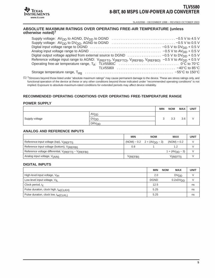
ABSOLUTE MAXIMUM RATINGS OVER OPERATING FREE-AIR TEMPERATURE (unlessotherwise noted) †
Supply voltage: AVDD to AGND, DVDD to DGND −0.5 V to 4.5 V. . . . . . . . . . . . . . . . . . . . . . . . . . . . . . . . . . . . Supply voltage: AVDD to DVDD, AGND to DGND −0.5 V to 0.5 V. . . . . . . . . . . . . . . . . . . . . . . . . . . . . . . . . . . . Digital input voltage range to DGND −0.5 V to DVDD + 0.5 V. . . . . . . . . . . . . . . . . . . . . . . . . . . . . . . . . . . . . . . . Analog input voltage range to AGND −0.5 V to AVDD + 0.5 V. . . . . . . . . . . . . . . . . . . . . . . . . . . . . . . . . . . . . . . . Digital output voltage applied from external source to DGND −0.5 V to DVDD + 0.5 V. . . . . . . . . . . . . . . . . . . Reference voltage input range to AGND: V(REFTI), V(REFTO), V(REFBI), V(REFBO) −0.5 V to AVDD + 0.5 VOperating free-air temperature range, TA: TLV5580C 0°C to 70°C. . . . . . . . . . . . . . . . . . . . . . . . . . . . . . . . . .
TLV5580I −40°C to 85°C. . . . . . . . . . . . . . . . . . . . . . . . . . . . . . . . . Storage temperature range, Tstg −55°C to 150°C. . . . . . . . . . . . . . . . . . . . . . . . . . . . . . . . . . . . . . . . . . . . . . . . . .
(1) †Stresses beyond those listed under “absolute maximum ratings” may cause permanent damage to the device. These are stress ratings only, andfunctional operation of the device at these or any other conditions beyond those indicated under “recommended operating conditions” is notimplied. Exposure to absolute-maximum-rated conditions for extended periods may affect device reliability.
RECOMMENDED OPERATING CONDITIONS OVER OPERATING FREE-TEMPERATURE RANGE
POWER SUPPLY
MIN NOM MAX UNIT
AVDDSupply voltage DVDD 3 3.3 3.6 VSupply voltage
DRVDD
3 3.3 3.6 V
ANALOG AND REFERENCE INPUTS
MIN NOM MAX UNIT
Reference input voltage (top), V(REFTI) (NOM) − 0.2 2 + (AVDD − 3) (NOM) + 0.2 V
Reference input voltage (bottom), V(REFBI) 0.8 1 1.2 V
Reference voltage differential, V(REFTI) − V(REFBI) 1 + (AVDD − 3) V
Analog input voltage, V(AIN) V(REFBI) V(REFTI) V
DIGITAL INPUTS
MIN NOM MAX UNIT
High-level input voltage, VIH 2.0 DVDD V
Low-level input voltage, VIL DGND 0.2xDVDD V
Clock period, tc 12.5 ns
Pulse duration, clock high, tw(CLKH) 5.25 ns
Pulse duration, clock low, tw(CLKL) 5.25 ns

SLAS205B − DECEMBER 1998 − REVISED OCTOBER 2003
www.ti.com
6
ELECTRICAL CHARACTERISTICS OVER RECOMMENDED OPERATING CONDITIONS WITH F CLK = 80MSPS AND USE OF EXTERNAL VOLTAGE REFERENCES (unless otherwise noted)
POWER SUPPLYPARAMETER TEST CONDITIONS MIN TYP MAX UNIT
AVDDAVDD = DVDD = 3.3 V, DRVDD = 3 V,
57 71
IDD Operating supply current DVDDAVDD = DVDD = 3.3 V, DRVDD = 3 V,CL = 15 pF, VI = 1 MHz, −1 dBFS
3 3.6 mAIDD Operating supply current
DRVDDCL = 15 pF, VI = 1 MHz, −1 dBFS
5 7.5
mA
PD Power dissipationPWDN_REF = L 213 270
PD Power dissipationPWDN_REF = H 165 210 mW
PD(STBY) Standby power STBY = H, CLK held high or low 11 15
mW
DIGITAL LOGIC INPUTSPARAMETER TEST CONDITIONS MIN TYP MAX UNIT
IIH High-level input current on CLK† AVDD = DVDD = DRVDD = CLK = 3.6 V 10 µA
IILLow-level input current on digital inputs (OE, STDBY, PWDN_REF, CLK)
AVDD = DVDD = DRVDD = 3.6 V,Digital inputs at 0 V
10 µA
CI Input capacitance 5 pF
† IIH leakage current on other digital inputs (OE, STDBY, PWDN_REF) is not measured since these inputs have an internal pull-down resistor of4 KΩ to DGND.
LOGIC OUTPUTSPARAMETER TEST CONDITIONS MIN TYP MAX UNIT
VOH High-level output voltageAVDD = DVDD = DRVDD = 3 V at IOH = 50 µA,Digital output forced high
2.8 V
VOL Low-level output voltageAVDD = DVDD = DRVDD = 3.6 V at IOL = 50 µA,Digital output forced low
0.1 V
CO Output capacitance 5 pF
IOZHHigh-impedance state output current tohigh level
AVDD = DVDD = DRVDD = 3.6 V
10 µA
IOZLHigh-impedance state output current tolow level
AVDD = DVDD = DRVDD = 3.6 V
10 µA

SLAS205B − DECEMBER 1998 − REVISED OCTOBER 2003
www.ti.com
7
ELECTRICAL CHARACTERISTICS OVER RECOMMENDED OPERATING CONDITIONS WITH F CLK = 80MSPS AND USE OF EXTERNAL VOLTAGE REFERENCES (unless otherwise noted)
DC ACCURACYPARAMETER TEST CONDITIONS MIN TYP MAX UNIT
Integral nonlinearity (INL), best-fit Internal references (see Note 1) TA = −40°C to 85°C −2.4 ±1 2.4 LSBIntegral nonlinearity (INL), best-fit Internal references (see Note 1) TA = −40°C to 85°C −2.4 ±1 2.4 LSB
Differential nonlinearity (DNL) Internal references (see Note 2) TA = −40°C to 85°C −1 ±0.6 1.3 LSB
Zero errorAVDD = DVDD = 3.3 V, DRVDD = 3 V See Note 3
5 %FS
Full scale errorAVDD = DVDD = 3.3 V, DRVDD = 3 V See Note 3
5 %FS
1. Integral nonlinearity refers to the deviation of each individual code from a line drawn from zero to full scale. The point used as zero occurs 1/2 LSB before the first code transition. The full−scale point is defined as a level 1/2 LSB beyond the last code transition. The deviationis measured from the center of each particular code to the true straight line between these two endpoints.
2. An ideal ADC exhibits code transitions that are exactly 1 LSB apart. DNL is the deviation from this ideal value. Therefore this measure indicateshow uniform the transfer function step sizes are. The ideal step size is defined here as the step size for the device under test (i.e., (last transitionlevel − first transition level) ÷ (2n − 2)). Using this definition for DNL separates the effects of gain and offset error. A minimum DNL better than −1LSB ensures no missing codes.
3. Zero error is defined as the difference in analog input voltage − between the ideal voltage and the actual voltage − that will switch the ADC outputfrom code 0 to code 1. The ideal voltage level is determined by adding the voltage corresponding to 1/2 LSB to the bottom reference level. Thevoltage corresponding to 1 LSB is found from the difference of top and bottom references divided by the number of ADC output levels (256).
Full-scale error is defined as the difference in analog input voltage – between the ideal voltage and the actual voltage – that will switch the ADCoutput from code 254 to code 255. The ideal voltage level is determined by subtracting the voltage corresponding to 1.5 LSB from the top referencelevel. The voltage corresponding to 1 LSB is found from the difference of top and bottom references divided by the number of ADC output levels(256).
ANALOG INPUTPARAMETER TEST CONDITIONS MIN TYP MAX UNIT
CI Input capacitance 4 pF
REFERENCE INPUT (AVDD = DVDD = DRVDD = 3.6 V)PARAMETER TEST CONDITIONS MIN TYP MAX UNIT
Rref Reference input resistance 200 Ω
Iref Reference input current 5 mA
REFERENCE OUTPUTSPARAMETER TEST CONDITIONS MIN TYP MAX UNIT
V(REFTO) Reference top offset voltage Absolute min/max values valid 2.07 2 + [(AVDD − 3) ÷ 2] 2.21 V
V(REFBO) Reference bottom offset voltageAbsolute min/max values validand tested for AVDD = 3.3 V 1.09 1 + [(AVDD − 3) ÷ 2] 1.21 V

SLAS205B − DECEMBER 1998 − REVISED OCTOBER 2003
www.ti.com
8
ELECTRICAL CHARACTERISTICS OVER RECOMMENDED OPERATING CONDITIONS WITH F CLK = 80MSPS AND USE OF EXTERNAL VOLTAGE REFERENCES (unless otherwise noted) (continued)DYNAMIC PERFORMANCE†
PARAMETER TEST CONDITIONS MIN TYP MAX UNIT
fin = 1 MHz 6.2 6.7
Effective number of bits, ENOBfin = 4.43 MHz 6.2 6.7
BitsEffective number of bits, ENOBfin = 15 MHz 6.4
Bits
fin = 76 MHz 6.5
fin = 1 MHz 39 42
Signal-to-total harmonic distortion + noise, S/(THD+N)fin = 4.43 MHz 39 42
dBSignal-to-total harmonic distortion + noise, S/(THD+N)fin = 15 MHz 40
dB
fin = 76 MHz 40
fin = 1 MHz −46 −50
Total harmonic distortion (THD)fin = 4.43 MHz −45.5 −49
dBTotal harmonic distortion (THD)fin = 15 MHz −44
dB
fin = 76 MHz −45.5
fin = 1 MHz 48 51
Spurious free dynamic range (SFDR)fin = 4.43 MHz 48 51
dBSpurious free dynamic range (SFDR)fin = 15 MHz 46
dB
fin = 76 MHz 48
Analog input full-power bandwidth, BW See Note 4 700 MHz
Differential phase, DP fclk = 40 MHz, fin = 4.43 MHz, 0.8 °Differential phase, DP fclk = 40 MHz, fin = 4.43 MHz,20 IRE amplitude vs. full-scale of 140 IRE
0.8 °
Differential gain, DG
fclk = 40 MHz, fin = 4.43 MHz,20 IRE amplitude vs. full-scale of 140 IRE 0.6 %Differential gain, DG 20 IRE amplitude vs. full-scale of 140 IRE 0.6 %
† Based on analog input voltage of −1 dBFS referenced to a 1.3 Vpp full-scale input range and using the external voltage references atfclk = 80 MSPS with AVDD = DVDD = 3.3 V and DRVDD = 3.0 V at 25°C.
4. The analog input bandwidth is defined as the maximum frequency of a −1 dBFS input sine that can be applied to the device for which an extra3 dB attenuation is observed in the reconstructed output signal.

SLAS205B − DECEMBER 1998 − REVISED OCTOBER 2003
www.ti.com
9
ELECTRICAL CHARACTERISTICS OVER RECOMMENDED OPERATING CONDITIONS WITH F CLK = 80MSPS AND USE OF EXTERNAL VOLTAGE REFERENCES (unless otherwise noted) (continued)
TIMING REQUIREMENTS
PARAMETER TEST CONDITIONS MIN TYP MAX UNIT
fclk Maximum conversion rate 80 MHz
fclk Minimum conversion rate 10 kHz
td(o) Output delay time (see Figure 1) CL = 10 pF, See Notes 5 and 6 4.5 9 ns
th(o) Output hold time CL = 2 pF, See Note 5 2 ns
td(pipe) Pipeline delay (latency) See Note 6 4.5 4.5 4.5CLK
cycles
td(a) Aperture delay time 3 ns
tj(a) Aperture jitterSee Note 5
1.5 ps, rms
tdis Disable time, OE rising to Hi-ZSee Note 5
5 8 ns
ten Enable, OE falling to valid data 5 8 ns
5. Output timing td(o) is measured from the 1.5 V level of the CLK input falling edge to the 10%/90% level of the digital output. The digital output loadis not higher than 10 pF.
Output hold time th(o) is measured from the 1.5 V level of the CLK input falling edge to the 10%/90% level of the digital output. The digital outputis load is not less than 2 pF.
Aperture delay td(A) is measured from the 1.5 V level of the CLK input to the actual sampling instant.
The OE signal is asynchronous.
OE timing tdis is measured from the VIH(MIN) level of OE to the high-impedance state of the output data. The digital output load is not higher than10 pF.
OE timing ten is measured from the VIL(MAX) level of OE to the instant when the output data reaches VOH(min) or VOL(max) output levels. The digitaloutput load is not higher than 10 pF.
6. The number of clock cycles between conversion initiation on an input sample and the corresponding output data being made available from theADC pipeline. Once the data pipeline is full, new valid output data is provided on every clock cycle. In order to know when data is stable on theoutput pins, the output delay time td(o) (i.e., the delay time through the digital output buffers) needs to be added to the pipeline latency. Note thatsince the max. td(o) is more than 1/2 clock period at 80 MHz; data cannot be reliably clocked in on a rising edge of CLK at this speed. The fallingedge should be used.
D0−D7 N−4 N−3 N−2 N−1 N N+1
N
N+1
N+2
N+3
N+4N+5
tj(A)
td(A)VIL
(max) 1.5 V
tw(CLKH)tw(CLKL)
1/fCLK
th(o)
1.5 V
td(o)
tdis ten
CLK
OE
90%
10%
VIH(min)
td(pipe)
VOH(min)
VOL(max)
VIL(max)
VIH(min)
Figure 1. Timing Diagram

SLAS205B − DECEMBER 1998 − REVISED OCTOBER 2003
www.ti.com
10
PERFORMANCE PLOTS AT 25 °C
−0.4
−10 50 100 150
DN
L −
LSB
0
0.6
ADC Code
1
200 250
0.8
0.4
0.2
−0.2
−0.6
−0.8
Figure 2. DNL vs Input Code At 80 MSPS (With External Reference, PW Package)
−1
−20 50 100 150
INL
− LS
B
0
1
ADC Code
2
200 250
1.5
0.5
−0.5
−1.5
Figure 3. INL vs Input Code At 80 MSPS (With External Reference, PW Package)

SLAS205B − DECEMBER 1998 − REVISED OCTOBER 2003
www.ti.com
11
PERFORMANCE PLOTS AT 25 °C (Continued)
80 MSPS40 MSPS
60 MSPS
25
20
10
00 10 20 30 40 50 60
S(T
HD
+N) −
dB
40
45
Analog Input Frequency − MHz
50
70 80 90 100
35
30
15
5
Figure 4. S/(THD+N) vs V IN At 80 MSPS (Internal Reference),60 MSPS (External Reference), 40 MSPS (External Reference)
−40
−60
−900 5 10 15 20 25 30
Pow
er −
dB
FS −30
−20
f − Frequency − MHz
−10
0
−50
−70
−80
Figure 5. Spectral Plot f IN = 1.011 MHz At 60 MSPS

SLAS205B − DECEMBER 1998 − REVISED OCTOBER 2003
www.ti.com
12
PERFORMANCE PLOTS AT 25 °C (Continued)
−70
−900 5 10 15 20 25
Pow
er −
dB
FS
−40
−20
f − Frequency − MHz
0
30 35 40
−10
−30
−50
−60
−80
Figure 6. Spectral Plot f IN = 0.996 MHz At 80MSPS
−40
−60
−900 5 10 15 20 25 30
Pow
er −
dB
FS −30
−20
f − Frequency − MHz
−10
35 40
0
−50
−70
−80
Figure 7. Spectral Plot f IN = 15.527 MHz At 80 MSPS
−40
−60
−900 5 10 15 20 25 30
Pow
er −
dB
FS −30
−20
f − Frequency − MHz
−10
35 40
0
−50
−70
−80
Figure 8. Spectral Plot f IN = 75.02 MHz At 80MSPS(Plot shows folded spectrum of undersampled input signal)

SLAS205B − DECEMBER 1998 − REVISED OCTOBER 2003
www.ti.com
13
PERFORMANCE PLOTS AT 25 °C (Continued)
100
50
00 10 20 30 40 50 60
Pow
er −
mW 150
200
Sampling Frequency − MHz
250
70 80 90 100
Figure 9. Power vs f CLK At VIN = 1 MHz, −1 dBFS
Figure 10. IDRVDD vs f CLK At VIN = 1 MHz, −1 dBFS
2.5
2
1
00 10 20 30 40 50 60
IDR
VD
D −
mA
3.5
4.5
Sampling Frequency − MHz
5
70 80 90 100
4
3
1.5
0.5
106
−5
−6
−8
−10
Fun
dam
enta
l Pow
er −
dB
FS
−3
−1
Analog Input Frequency − Hz
0
−2
−4
−7
−9
107 108 109
Figure 11. ADC Output Power With Respect To −1 dBFS V IN(Internal Reference, DW Package)

SLAS205B − DECEMBER 1998 − REVISED OCTOBER 2003
www.ti.com
14
PRINCIPLE OF OPERATION
The TLV5580 implements a high-speed 80 MSPS converter in a cost-effective CMOS process. Powered from3.3 V, the single-pipeline design architecture ensures low-power operation and 8 bit accuracy. Signal input andclock signals are all single-ended. The digital inputs are 3.3 V TTL/CMOS compatible. Internal voltagereferences are included for both bottom and top voltages. Therefore the converter forms a self-containedsolution. Alternatively the user may apply externally generated reference voltages. In doing so, both input offsetand input range can be modified to suit the application.
A high-speed sampling-and-hold captures the analog input signal. Multiple stages will generate the output codewith a pipeline delay of 4.5 CLK cycles. Correction logic combines the multistage data and aligns the 8-bit outputword. All digital logic operates at the rising edge of CLK.
ANALOG INPUT
AIN
CI
S1
RSW
RS
VS
TLV5580
Figure 12. Simplified Equivalent Input Circuit
A first-order approximation for the equivalent analog input circuit of the TLV5580 is shown in Figure 12. Theequivalent input capacitance CI is 4 pF typical. The input must charge/discharge this capacitance within thesample period of one half clock cycle. When a full-scale voltage step is applied, the input source provides thecharging current through the switch resistance RSW (200 Ω) of S1 and quickly settles. In this case the inputimpedance is low. Alternatively, when the source voltage equals the value previously stored on CI, the holdcapacitor requires no input current and the equivalent input impedance is very high.
To maintain the frequency performance outlined in the specifications, the total source impedance should belimited to about 80 Ω, as follows from the equation with fCLK = 80 MHz, CI = 4 pF, RSW = 200 Ω :
RS 1 ÷ 2fCLK CI In(256)–RSW
So, for applications running at a lower fCLK, the total source resistance can increase proportionally.

SLAS205B − DECEMBER 1998 − REVISED OCTOBER 2003
www.ti.com
15
PRINCIPLE OF OPERATIONDC COUPLED INPUT
_+
AVDD
VIN
REFTI
REFTO
REFBI
REFBO
AINTLV5580 _
+VREF
VIN
REFTI
REFTO
REFBI
REFBO
AINTLV5580
RIN
R1
RIN
R2
(a) (b)
Figure 13. DC-Coupled Input Circuit
For dc-coupled systems an op amp can level-shift a ground-referenced input signal. A circuit as shown inFigure 13(a) is acceptable. Alternatively, the user might want a bipolar shift together with the bottom referencevoltage as seen in Figure 13(b). In this case the AIN voltage is given by:
AIN 2 R2 ÷ R1 R2 VREF – VIN
AC COUPLED INPUT
VIN AINTLV5580R1
R2
VBIAS+
−
C1
C2
Figure 14. AC-Coupled Input Circuit
For many applications, especially in single supply operation, ac coupling offers a convenient way for biasingthe analog input signal at the proper signal range. Figure 14 shows a typical configuration. To maintain theoutlined specifications, the component values need to be carefully selected. The most important issue is thepositioning of the 3 dB high-pass corner point f−3 dB, which is a function of R2 and the parallel combination ofC1 and C2, called Ceq. This is given by the following equation:
f–3 dB 1 ÷ 2π x R2 x Ceqwhere Ceq is the parallel combination of C1 and C2.
Since C1 is typically a large electrolytic or tantalum capacitor, the impedance becomes inductive at higherfrequencies. Adding a small ceramic or polystyrene capacitor, C2 of approximately 0.01 µF, which is notinductive within the frequency range of interest, maintains low impedance. If the minimum expected input signalfrequency is 20 kHz, and R2 equals 1 kΩ and R1 equals 50 Ω, the parallel capacitance of C1 and C2 must bea minimum of 8 nF to avoid attenuating signals close to 20 kHz.

SLAS205B − DECEMBER 1998 − REVISED OCTOBER 2003
www.ti.com
16
PRINCIPLE OF OPERATIONREFERENCE TERMINALS
The voltages on terminals REFBI and REFTI determine the TLV5580’s input range. Since the device has aninternal voltage reference generator with outputs available on REFBO respectively REFTO, correspondingterminals can be directly connected externally to provide a contained ADC solution. Especially at highersampling rates, it is advantageous to have a wider analog input range. The wider analog input range isachievable by using external voltage references (e.g., at AVDD = 3.3 V, the full scale range can be extendedfrom 1 Vpp (internal reference) to 1.3 Vpp (external reference) as shown in Table 1). These voltages shouldnot be derived via a voltage divider from a power supply source. Instead, use a bandgap-derived voltagereference to derive both references via an op amp circuit. Refer to the schematic of the TLV5580 evaluationmodule for an example circuit.
When using external references, the full-scale ADC input range and its dc position can be adjusted. Thefull-scale ADC range is always equal to VREFT – VREFB. The maximum full-scale range is dependent on AVDDas shown in the specification section. In addition to the limitation on their difference, VREFT and VREFB eachalso have limits on their useful range. These limits are also dependent on AVDD.Table 3 summarizes these limits for 3 cases.
Table 1. Recommended Operating Modes
AVDD VREFB(min) VREFB(max) VREFT(min) VREFT(max) [VREFT−VREFB]max3 V 0.8 V 1.2 V 1.8 V 2.2 V 1 V
3.3 V 0.8 V 1.2 V 2.1 V 2.5 V 1.3 V
3.6 V 0.8 V 1.2 V 2.4 V 2.8 V 1.6 V
DIGITAL INPUTS
The digital inputs are CLK, STDBY, PWDN_REF, and OE. All these signals, except CLK, have an internalpull-down resistor to connect to digital ground. This provides a default active operation mode using internalreferences when left unconnected.
The CLK signal at high frequencies should be considered as an analog input. Overshoot/undershoot shouldbe minimized by proper termination of the signal close to the TLV5580. An important cause of performancedegradation for a high-speed ADC is clock jitter. Clock jitter causes uncertainty in the sampling instant of theADC, in addition to the inherent uncertainty on the sampling instant caused by the part itself, as specified byits aperture jitter. There is a theoretical relationship between the frequency (f) and resolution (2N) of a signalthat needs to be sampled and the maximum amount of aperture error dtmax that is tolerable. The followingformula shows the relation:
dtmax 1 f 2N1
As an example, for an 8−bit converter with a 15-MHz input, the jitter needs to be kept <41 pF in order not tohave changes in the LSB of the ADC output due to the total aperture error.

SLAS205B − DECEMBER 1998 − REVISED OCTOBER 2003
www.ti.com
17
PRINCIPLE OF OPERATIONDIGITAL OUTPUTS
The output of TLV5580 is a standard binary code. Capacitive loading on the output should be kept as low aspossible (a maximum loading of 10 pF is recommended) to provide best performance. Higher output loadingcauses higher dynamic output currents and can increase noise coupling into the device’s analog front end. Todrive higher loads, use an output buffer is recommended.
When clocking output data from TLV5580, it is important to observe its timing relation to CLK. Pipeline ADCdelay is 4.5 clock cycles to which the maximum output propagation delay is added. See Note 6 in thespecification section for more details.
LAYOUT, DECOUPLING AND GROUNDING RULES
It is necessary for any PCB using the TLV5580 to have proper grounding and layout to achieve the statedperformance. Separate analog and digital ground planes that are spliced underneath the device are advisable.TLV5580 has digital and analog terminals on opposite sides of the package to make proper grounding easier.Since there is no internal connection between analog and digital grounds, they have to be joined on the PCB.Joining the digital and analog grounds at a point in close proximity to the TLV5580 is advised.
As for power supplies, separate analog and digital supply terminals are provided on the device (AVDD/DVDD).The supply to the digital output drivers is kept separate also (DRVDD). Lowering the voltage on this supply fromthe nominal 3.3 V to 3 V improves performance because of the lower switching noise caused by the outputbuffers.
Due to the high sampling rate and switched-capacitor architecture, TLV5580 generates transients on the supplyand reference lines. Proper decoupling of these lines is essential. Decoupling as shown in the schematic of theTLV5580 EVM is recommended.

SLAS205B − DECEMBER 1998 − REVISED OCTOBER 2003
www.ti.com
18
TLV5580 EVALUATION MODULE
TLV5580 EVALUATION MODULE
TI provides an evaluation module (EVM) for TLV5580. The EVM also includes a 10-bit 80 MSPS DAC so thatthe user can convert the digitized signal back to the analog domain for functional testing. Performancemeasurements can be done by capturing the ADC’s output data.
The EVM provides the following additional features:
Provision of footprint for the connection of an onboard crystal oscillator, instead of using an external clock input.
Use of TLV5580 internal or external voltage references. In the case of external references, an onboard circuitis used that derives adjustable bottom and top reference voltages from a bandgap reference. Two potentiometersallow for the independent adjustments of both references. The full scale ADC range can be adjusted to the inputsignal amplitude.
All digital output, control signal I/O (output enable, standby, reference power-down) and clock I/O are providedon a single connector. The EVM can thus be part of a larger (DSP) system for prototyping.
Onboard prototyping area with analog and digital supply and ground connections.
Figure 15 shows the EVM schematic.
The EVM is factory shipped for use in the following configuration:
Use of external (onboard) voltage references
External clock input
ANALOG INPUT
A signal in the range between V(REFBI) and V(REFTI) should be applied to avoid overflow/underflow on connectorJ10. This signal is onboard terminated with 50Ω. There is no onboard biasing of the signal. When using external(onboard) references, these levels can be adjusted with R7 (V(REFTI)) and R6 (V(REFBI)). Adjusting R7 causesboth references to shift. R6 only impacts the bottom reference. The range of these signals for which the deviceis specified depends on AVDD and is shown under the Recommended Operating Conditions.
Internally generated reference levels are also dependent on AVDD as shown in the electrical characteristicssection.
CLOCK INPUT
A clock signal should be applied with amplitudes ranging from 0 to AVDD with a frequency equal to the desiredsampling frequency on connector J9. This signal is onboard terminated with 50 Ω. Both ADC and DAC run offthe same clock signal. Alternatively the clock can be applied from terminal 1 on connector J11. A third optionis using a crystal oscillator. The EVM board provides the footprint for a crystal oscillator that can be populatedby the end-user, depending on the desired frequency. The footprint is compatible with the Epson EG-8002DCseries of programmable high-frequency crystal oscillators. Refer to the TLV5580 EVM Settings for selectingbetween the different clock modes.

SLAS205B − DECEMBER 1998 − REVISED OCTOBER 2003
www.ti.com
19
TLV5580 EVALUATION MODULE
POWER SUPPLIES
The board provides seven power supply connectors (see Table 2). For optimum performance, analog and digitalsupplies should be kept separate. Using separate supplies for the digital logic portion of TLV5580 (DVDD) andits output drivers (DRVDD) benefits dynamic performance, especially when DRVDD is put at the minimumrequired voltage (3 V), while DVDD might be higher (up to 3.6 V). This lowers the switching noise on the diecaused by the output drivers.
Table 2. Power Supplies
SIGNALNAME
CONNECTORBOARDLABEL
DESCRIPTION
DRV3 J1 3DRV 3.3 V digital supply for TLV5580 (digital output drivers)
DV3 J2 3VD 3.3 V digital supply for TLV5580 (digital logic) and peripherals
DV5 J3 5VD 5 V digital supply for D/A converter and peripherals
AV3 J4 3VA 3.3 V analog supply for TLV5580
AV5 J5 5VA 5 V analog supply for onboard reference circuit and D/A converter. Can be left unconnected ifinternal references are used and no D/A conversion is required.
AV+12 J6 12VA 12 V analog supply for onboard reference circuit. Can be left unconnected if internal referencesare used.
AV−12 J7 −12VA −12 V analog supply for onboard reference circuit. Can be left unconnected if internal referencesare used.
VOLTAGE REFERENCES
SW1 and SW2 switch between internal and external top and bottom references respectively. The externalreferences are onboard generated from a stable bandgap-derived 3.3 V signal (using TI’s TPS7133 andquad-op amp TLE2144). They can be adjusted via potentiometers R6 (V(REFBI)) and R7 (V(REFTI)). It is advisedto power down the internal voltage references by asserting PWN_REF when onboard references are used.
The references are measured at test points TP3 (V(REFB)) and TP4 (V(REFT)).
DAC OUTPUT
The onboard DAC is a 10-bit 80 MSPS converter. It is connected back-to-back to the TLV5580. While the usercould use its analog output for measurements, the DAC output is directly connected to connector J8 and doesnot pass through an analog reconstruction filter. So mirror spectra from aliased signal components feed throughinto the analog output.
For this reason and to separate ADC and DAC contributions, performance measurements should be made bycapturing the ADC output data available on connector J11 and not by evaluating the DAC output.

SLAS205B − DECEMBER 1998 − REVISED OCTOBER 2003
www.ti.com
20
TLV5580 EVALUATION MODULETLV5580 EVM SETTINGS
CLOCK INPUT SETTINGSREFERENCEDESIGNATOR
FUNCTION
W1 Clock selection switch1−2 J11: clock from pin1 on J11 connector2−3 J9: clock from J9 SMA connector
W2 Clock source switch XTL: clock from onboard crystal oscillator
CLK: clock from pin 1 on J11 connector (if W1/1−2) or J9 SMA connector (if W1/2−3)NOTE: If set to XTL and a XTL oscillator is populated, no clock signal should be applied to J9 or J11, depending on the W1setting.
W3 Clock output switch1−2 Rising: clock output on J11 connector is the same phase as the clock to the digital output buffer. Data changes on risingCLK edge.2−3 Falling: clock output on J11 connector is the opposite phase as the digital output buffer. Data changes on falling CLK edge.
REFERENCE SETTINGSREFERENCEDESIGNATOR
FUNCTION
SW1 REFT external/internal switch REFT internal: REFT from TLV5580 internal reference
REFT external: REFT from onboard voltage reference circuit
SW2 REFB external/internal switch REFB internal: REFB from TLV5580 internal reference
REFB external: REFB from onboard voltage reference circuitCONTROL SETTINGS
REFERENCEDESIGNATOR
FUNCTION
W4 TLV5580 and digital output buffer output enable control (1) 5580-574 OE-connected: Connects OEs of TLV5580 and digital output buffer (574 buffer). Use this when no board-externalOE is used. In addition, close W5 to have both OEs permanently enabled.
5580-574 OE-disconnected: Disconnects OEs of TLV5580 and digital output buffer (574 buffer). The OE for the output bufferneeds to be pulled low from pin 5 on J11 connector to enable. The OE for TLV5580 is independently controlled from pin 7 onJ11 connector (W5 open) or is permanently enabled if W5 is closed.
W5 TLV5580 and digital output buffer output enable control (2) 5580 OE to GND: Connects OEs of TLV5580 to GND. Additionally connects OE of 74ALS574 to GND if W4 is 5580-574OE-connected.
5580 OE external: Enables control of OE of TLV5580 via pin 7 on J11 connector. When taken high (internal pulldown) theoutput can be disabled.
W6 TLV5580 STDBY control Stdby: STDBY is active (high).
Active: STDBY is low, via internal pulldown. STDBY can be taken high from pin 9 on J11 connector to enable standby mode.
SLAS205B − DECEMBER 1998 − REVISED OCTOBER 2003
www.ti.com
21
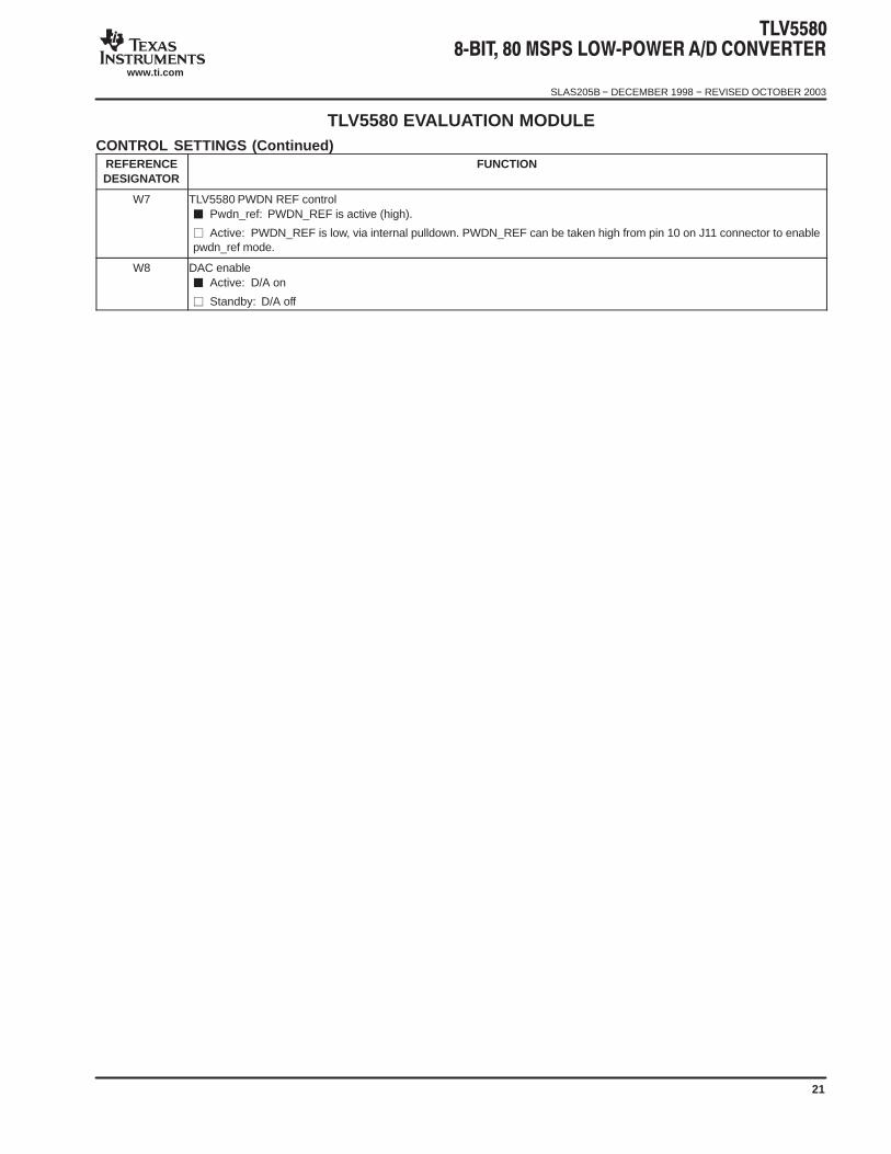
TLV5580 EVALUATION MODULECONTROL SETTINGS (Continued)
REFERENCEDESIGNATOR
FUNCTION
W7 TLV5580 PWDN REF control Pwdn_ref: PWDN_REF is active (high).
Active: PWDN_REF is low, via internal pulldown. PWDN_REF can be taken high from pin 10 on J11 connector to enablepwdn_ref mode.
W8 DAC enable Active: D/A on
Standby: D/A off

SLAS205B − DECEMBER 1998 − REVISED OCTOBER 2003
www.ti.com
22
AVS
SN
CD
VS
SD
VD
DN
CD
0D
1D
2
D3D4D5D6D7D8D9
NC
IO
CE
NC
DV
SS
VB
DV
DD
NC
BLK
CLK
IOVG
AVDDAVDDVREFSREF
IREF
25 26 27 28 29 30 31 32
1234567
8
11 16 15 14 13 12 10 9
C30
.1 µ
F
DV
5
24232221201918
17
R3
200
C25
.1 µ
F
R4
3.24
kΩ U3
C26
.1 µ
F
CX
D23
06Q
C29
.1 µ
FDV
5
C28
.1 µ
F
R11
10 k
ΩD
V5
R14
10 k
ΩD
V5
W8
R25R23R22R21R20R19R18
20202020202020
R24 20
10 k
Ω10
kΩ
10 k
Ω10
kΩ
10 k
Ω10
kΩ
10 k
Ω10
kΩ
R48
R47
R46
R45
R44
R43
R42
R41
DV
519 18 17 16 15 14 13 12
1Q 2Q 3Q 4Q 5Q 6Q 7Q 8QD
GN
D
DV
320 10
1D 2D 3D 4D 5D 6D 7D 8DOC
CLK
1 11 2 3 4 5 6 7 8 9
U5
C41
.1 µ
F
DV
3
SN
74LV
T57
4DW
20 20 20 20 20 20 20 20
R39
R38
R36
R35
R33
R32
R31
R30
C24
.1 µ
F
DV
5D
V5
OE
OU
T
VC
C
GN
D
W2 12 13
11R
13 20
J9C
LOC
K I
N
J8
DA
C_O
UT
AV5
R29 20
U2D
SN
74A
LVC
00
9 108
R17 20
U2C
1 23
U2A
4 56
U2B
W3
R37 20
CLK
_OU
T
123456789
1011121314151617181920212223242526
W1
3
2
1
R28
49.9
CLK
_IN
Q(0
−7)
Q7
Q6
Q5
Q4
Q3
Q2
Q1
Q0
W4
1D
RV
DD
AVS
S28
2 3 4 5 6 7 8 9 10 11 12 13 14
U6 D0
D1
D2
D3
D4
D5
D6
D7
DR
VS
SD
VS
SC
LKO
ED
VD
D
27 26 25 24 23 22 21 20 19 18 17 16 15
AVD
DA
INC
ML
PW
DN
_RE
FAV
SS
RE
FB
OR
EF
BI
RE
FT
IR
EF
TO
AVS
SB
GAV
DD
ST
DB
Y
R40
10 k
Ω
DR
V3
C45
.1 µ
F
C35
.1 µ
F
DV
3
TLV
5580
PW
W5
W6
C33
.1 µ
F
C34
.1 µ
F
AV3
W7
DV
3
C42
.1 µ
F
C46
.1 µ
F
AV3
J10
AN
ALO
G I
N
R34
49.9
C36
.01
µF
C39
.1 µ
F
+C
3810
µF
C37
.01
µF
C43
.1 µ
F
+C
4410
µF
SW
2S
W1
RE
FB
O
EX
T_R
EF
BE
XT
_RE
FT
RE
FT
O
RE
FB
IR
EF
TI
TP
3T
P4
C40
.1 µ
F
3IN
3IN
− +3O
UT
11 1210
4IN
4IN
− +4O
UT
15 1416
U4C
U4D
1IN
1IIN
− +1O
UT
2 31
U4A
R7
1 kΩ
R8
1 kΩ
RE
F3V
R9
1 kΩ
R12
1 kΩ
R16
1 kΩ
R27 10
EX
T_R
EF
T
R6
5 kΩ
R5
2.1
kΩ
RE
F3V
2IN
2IN
− +2O
UT
6 57
U4B
C32
.1 µ
FAV
−12
C31
.1 µ
F
AV +
12
R15
1 kΩ
EX
T_R
EF
BR
26 10
TLE
2144
CD
W
IN IN EN
GN
D
PG
OU
T
OU
T
SE
NS
E
R1
10 k
Ω3 4 2 1
8 6 5 7
+C
2310
µF
C27
.1 µ
F+
C22
10µ
F
AV5
RE
F3V
TP
1T
P2
R2 0
1 kΩ
R10
TLE
2144
CD
W
J11
X1
4 13
U1
TP
S71
33Q
D
SN
74A
LVC
00
SN
74A
LVC
00
SN
74A
LVC
00
Figure 15. EVM Schematic

SLAS205B − DECEMBER 1998 − REVISED OCTOBER 2003
www.ti.com
23
TLV5580 EVALUATION MODULE
++C20
10 µFC12
10 µFC111 µF
L6
4.7 µH1
2
J6
Analog +12 V
AV +12 V
C2110 µF
C1410 µF
C131 µF
L7
4.7 µH1
2
J7
Analog −12 V
AV −12 V
+ +
++C19
10 µFC10
10 µFC91 µF
L5
4.7 µH1
2
J5
Analog +5 V
AV5
++C18
10 µFC8
10 µFC71 µF
L4
4.7 µH1
2
J4
Analog +3.3 V
AV3
++C17
10 µFC6
10 µFC51 µF
L3
4.7 µH1
2
J3
Digital +5 V
DV5
++C16
10 µFC4
10 µFC31 µF
L2
4.7 µH1
2
J2
Digital +3.3 V (DVDD)
DV3
++C15
10 µFC2
10 µFC11 µF
L1
4.7 µH1
2
J1
Digital +3.3 V (DRVDD)
DRV3
Figure 15. EVM Schematic (Continued)

SLAS205B − DECEMBER 1998 − REVISED OCTOBER 2003
www.ti.com
24
TLV5580 EVALUATION MODULE
Top Overlay
Figure 15. EVM Schematic (Continued)

SLAS205B − DECEMBER 1998 − REVISED OCTOBER 2003
www.ti.com
25
TLV5580 EVALUATION MODULE
Top Layer
Figure 15. EVM Schematic (Continued)

SLAS205B − DECEMBER 1998 − REVISED OCTOBER 2003
www.ti.com
26
TLV5580 EVALUATION MODULE
Internal Plane 1
Figure 15. EVM Schematic (Continued)

SLAS205B − DECEMBER 1998 − REVISED OCTOBER 2003
www.ti.com
27
TLV5580 EVALUATION MODULE
Internal Plane 2
Figure 15. EVM Schematic (Continued)

SLAS205B − DECEMBER 1998 − REVISED OCTOBER 2003
www.ti.com
28
TLV5580 EVALUATION MODULE33
50 (m
il)
4200 (mil)
Drill Drawing for Through Hole
Figure 15. EVM Schematic (Continued)

SLAS205B − DECEMBER 1998 − REVISED OCTOBER 2003
www.ti.com
29
TLV5580 EVALUATION MODULE
Bottom Layer
Figure 15. EVM Schematic (Continued)

SLAS205B − DECEMBER 1998 − REVISED OCTOBER 2003
www.ti.com
30
TLV5580 EVALUATION MODULE
Table 3. TLV5580EVM Bill of Material
QTY. REFERENCE DESIGNATOR VALUE SIZE DESCRIPTIONMANUFACTURER/PART NUMBER†
7 C1, C11, C13, C3, C5, C7, C9 1 µF 1206 ceramic multi-layer capacitor Any
18 C10, C12, C14, C15, C16, C17,C18, C19, C2, C20, C21, C22,C23, C4, C6, C8, C38, C44
10 µF 3216 16 V, 10 µF, tantalum capacitor Any
2 C36, C43 0.01 µF 805 Ceramic multi-layer Any
19 C24, C25, C26, C27, C28, C29,C30, C31, C32, C33, C34, C35,C37, C39, C40, C41, C42, C45,C46
0.1 µF 805 Ceramic multi-layer capacitor Any
7 J1, J2, J3, J4, J5, J6, J7 Screw Con 2 terminal screw connector LumbergKRMZ2
3 J10, J8, J9 SMA PCM mount, SMA Jack Johnson Components142-0701-206
1 J11 IDC26 13 × 2.025 square pin header SamtecTSW-113-07-L-D
7 L1, L2, L3, L4, L5, L6, L7 4.7 µH 4.7 µH DO1608C-472-Coil Craft Coil CraftDO1608-472
1 R2 0 1206 Chip resistor Any
2 R26, R27 10 1206 Chip resistor Any
12 R1, R11, R14, R40, R41, R42,R43, R44, R45, R46, R47, R48
10 K 1206 Chip resistor Any
6 R10, R12, R15, R16, R8, R9 1 K 1206 Chip resistor Any
1 R5 2.1 K 1206 Chip resistor Any
20 R13, R17, R18, R19, R20, R21,R22, R23, R24, R25, R29, R30,R31, R32, R33, R35, R36, R37,R38, R39
20 1206 Chip resistor Any
1 R3 200 1206 Chip resistor Any
1 R4 3.24 K 1206 Chip resistor Any
2 R28, R34 49.9 1206 Chip resistor Any
1 R6 5 K 4 mm SM pot-top adjust Bourns3214W-5K
1 R7 1 K 4 mm SM pot-top adjust Bourns3214W-1K
2 SW1, SW2 SPDT C&K tiny series−slide switch C&KTS01CLE
4 TP1, TP2, TP3, TP4 TP Test point, single 0.025 pin SamtecTSW-101-07-L-Sor equivalent
1 U3 CXD2306Q SonyCXD2306Q
1 U2 SN74ALVC00D 14-SOIC (D) Quad 2-input positive NAND Texas InstrumentsSN74ALVC00D
1 U5 SN74LVT574DW 20-SOP (DW) Texas InstrumentsSN74LVT574DW
† Manufacturer and part number data for reference only. Equivalent parts might be substituted on the EVM.

SLAS205B − DECEMBER 1998 − REVISED OCTOBER 2003
www.ti.com
31
TLV5580 EVALUATION MODULETable 3. TLV5580EVM Bill of Material (Continued)
QTY. REFERENCE DESIGNATOR VALUE SIZE DESCRIPTIONMANUFACTURER/PART NUMBER†
1 U4 TLE2144CDW 16-SOP(D) Quad op amp Texas InstrumentsTLE2144CDW/TLE2144IDW
1 U6 TLV5580PW 28-TSSOP (PW) Texas InstrumentsTLV5580PW
1 U1 TPS7133 8-SOP(D) Low-dropout voltage regulator Texas InstrumentsTPS7133QD
6 W2, W4, W5, W6, W7, W8 SPST 2 position jumper, 0.1 spacing SamtecTSW-102-07-L-Sor equivalent
2 W1, W3 DPFT 3 position jumper, 0.1 spacing SamtecTSW-103-07-L-Sor equivalent
1 X1 NA Crystal oscillator EpsonSG-8002DC series
† Manufacturer and part number data for reference only. Equivalent parts might be substituted on the EVM.


MECHANICAL DATA
MTSS001C – JANUARY 1995 – REVISED FEBRUARY 1999
POST OFFICE BOX 655303 • DALLAS, TEXAS 75265
PW (R-PDSO-G**) PLASTIC SMALL-OUTLINE PACKAGE14 PINS SHOWN
0,65 M0,10
0,10
0,25
0,500,75
0,15 NOM
Gage Plane
28
9,80
9,60
24
7,90
7,70
2016
6,60
6,40
4040064/F 01/97
0,30
6,606,20
8
0,19
4,304,50
7
0,15
14
A
1
1,20 MAX
14
5,10
4,90
8
3,10
2,90
A MAX
A MIN
DIMPINS **
0,05
4,90
5,10
Seating Plane
0°–8°
NOTES: A. All linear dimensions are in millimeters.B. This drawing is subject to change without notice.C. Body dimensions do not include mold flash or protrusion not to exceed 0,15.D. Falls within JEDEC MO-153

IMPORTANT NOTICE
Texas Instruments Incorporated and its subsidiaries (TI) reserve the right to make corrections, modifications,enhancements, improvements, and other changes to its products and services at any time and to discontinueany product or service without notice. Customers should obtain the latest relevant information before placingorders and should verify that such information is current and complete. All products are sold subject to TI’s termsand conditions of sale supplied at the time of order acknowledgment.
TI warrants performance of its hardware products to the specifications applicable at the time of sale inaccordance with TI’s standard warranty. Testing and other quality control techniques are used to the extent TIdeems necessary to support this warranty. Except where mandated by government requirements, testing of allparameters of each product is not necessarily performed.
TI assumes no liability for applications assistance or customer product design. Customers are responsible fortheir products and applications using TI components. To minimize the risks associated with customer productsand applications, customers should provide adequate design and operating safeguards.
TI does not warrant or represent that any license, either express or implied, is granted under any TI patent right,copyright, mask work right, or other TI intellectual property right relating to any combination, machine, or processin which TI products or services are used. Information published by TI regarding third-party products or servicesdoes not constitute a license from TI to use such products or services or a warranty or endorsement thereof.Use of such information may require a license from a third party under the patents or other intellectual propertyof the third party, or a license from TI under the patents or other intellectual property of TI.
Reproduction of information in TI data books or data sheets is permissible only if reproduction is withoutalteration and is accompanied by all associated warranties, conditions, limitations, and notices. Reproductionof this information with alteration is an unfair and deceptive business practice. TI is not responsible or liable forsuch altered documentation.
Resale of TI products or services with statements different from or beyond the parameters stated by TI for thatproduct or service voids all express and any implied warranties for the associated TI product or service andis an unfair and deceptive business practice. TI is not responsible or liable for any such statements.
Following are URLs where you can obtain information on other Texas Instruments products and applicationsolutions:
Products Applications
Amplifiers amplifier.ti.com Audio www.ti.com/audio
Data Converters dataconverter.ti.com Automotive www.ti.com/automotive
DSP dsp.ti.com Broadband www.ti.com/broadband
Interface interface.ti.com Digital Control www.ti.com/digitalcontrol
Logic logic.ti.com Military www.ti.com/military
Power Mgmt power.ti.com Optical Networking www.ti.com/opticalnetwork
Microcontrollers microcontroller.ti.com Security www.ti.com/security
Telephony www.ti.com/telephony
Video & Imaging www.ti.com/video
Wireless www.ti.com/wireless
Mailing Address: Texas Instruments
Post Office Box 655303 Dallas, Texas 75265
Copyright 2004, Texas Instruments Incorporated