drv5012 datasheet - texas · pdf filetemperature ( qc) average supply current (p a)-40 -10 20...
TRANSCRIPT

Temperature (qC)
Ave
rage
Sup
ply
Cur
rent
(P
A)
-40 -10 20 50 800
0.5
1
1.5
2
2.5
3
D016
1.65 V3 V5.5 V
DRV5012
VCC
Controller
VCC
GND
OUT
SEL
GPIO
NS
S
S
S N
N
N
GPIO
Copyright © 2017, Texas Instruments Incorporated
Product
Folder
Order
Now
Technical
Documents
Tools &
Software
Support &Community
An IMPORTANT NOTICE at the end of this data sheet addresses availability, warranty, changes, use in safety-critical applications,intellectual property matters and other important disclaimers. PRODUCTION DATA.
DRV5012SLVSDD5 –AUGUST 2017
DRV5012 Ultra-Low-Power Digital-Latch Hall-Effect Sensor
1
1 Features1• Industry-Leading Low-Power Consumption• Pin-Selectable Sampling Rate:
– SEL = Low: 20 Hz Using 1.3 µA (1.8 V)– SEL = High: 2.5 kHz Using 142 µA (1.8 V)
• 1.65- to 5.5-V Operating VCC Range• High Magnetic Sensitivity: ±2 mT (Typical)• Robust Hysteresis: 4 mT (Typical)• Push-Pull CMOS Output• Small and Thin X2SON Package• –40°C to +85°C Operating Temperature Range
2 Applications• Brushless DC Motor Sensors• Incremental Rotary Encoding:
– Motor Speed– Mechanical Travel– Fluid Measurement– Knob Turning– Wheel Speed
• Portable Medical Devices• E-Locks, E-Bikes, Motorized Blinds• Flow Meters• Contactless Activation
3 DescriptionThe DRV5012 device is an ultra-low-power digital-latch Hall effect sensor with a pin-selectable samplingrate.
When a south magnetic pole is near the top of thepackage and the BOP threshold is exceeded, thedevice drives a low voltage. The output stays low untila north pole is applied and the BRP threshold iscrossed, which causes the output to drive a highvoltage. Alternating north and south poles arerequired to toggle the output, and integratedhysteresis separates BOP and BRP to provide robustswitching.
Using an internal oscillator, the DRV5012 devicesamples the magnetic field and updates the output ata rate of 20 Hz or 2.5 kHz, depending on the SEL pin.This dual-bandwidth feature can allow systems tomonitor changes in movement while using minimalpower.
The device operates from a VCC range of 1.65 V to5.5 V, and is packaged in a small X2SON.
Device Information(1)
PART NUMBER PACKAGE BODY SIZE (NOM)DRV5012 X2SON (4) 1.10 mm × 1.40 mm
(1) For all available packages, see the orderable addendum atthe end of the data sheet.
Typical Schematic Current Consumption in 20-Hz Mode

2
DRV5012SLVSDD5 –AUGUST 2017 www.ti.com
Product Folder Links: DRV5012
Submit Documentation Feedback Copyright © 2017, Texas Instruments Incorporated
Table of Contents1 Features .................................................................. 12 Applications ........................................................... 13 Description ............................................................. 14 Revision History..................................................... 25 Pin Configuration and Functions ......................... 36 Specifications......................................................... 3
6.1 Absolute Maximum Ratings ...................................... 36.2 ESD Ratings ............................................................ 36.3 Recommended Operating Conditions....................... 46.4 Thermal Information .................................................. 46.5 Electrical Characteristics........................................... 56.6 Magnetic Characteristics........................................... 56.7 Typical Characteristics .............................................. 6
7 Detailed Description .............................................. 77.1 Overview ................................................................... 77.2 Functional Block Diagram ......................................... 77.3 Feature Description................................................... 7
7.4 Device Functional Modes........................................ 108 Application and Implementation ........................ 11
8.1 Application Information............................................ 118.2 Typical Applications ............................................... 118.3 Do's and Don'ts....................................................... 15
9 Power Supply Recommendations ...................... 1610 Layout................................................................... 16
10.1 Layout Guidelines ................................................. 1610.2 Layout Example .................................................... 16
11 Device and Documentation Support ................. 1711.1 Device Support...................................................... 1711.2 Receiving Notification of Documentation Updates 1711.3 Community Resources.......................................... 1711.4 Trademarks ........................................................... 1711.5 Electrostatic Discharge Caution............................ 1711.6 Glossary ................................................................ 17
12 Mechanical, Packaging, and OrderableInformation ........................................................... 17
4 Revision HistoryNOTE: Page numbers for previous revisions may differ from page numbers in the current version.
DATE REVISION NOTESAugust 2017 * Initial release.

1 4
2 3
GND
VCC SEL
OUT
Thermal Pad
3
DRV5012www.ti.com SLVSDD5 –AUGUST 2017
Product Folder Links: DRV5012
Submit Documentation FeedbackCopyright © 2017, Texas Instruments Incorporated
5 Pin Configuration and Functions
DMR Package4-Pin X2SON With Exposed Thermal Pad
Top View
Pin FunctionsPIN
I/O DESCRIPTIONNAME NO.GND 2 — Ground referenceOUT 3 O Push-pull CMOS output. Drives a VCC or ground level.SEL 4 I CMOS input that selects the sampling rate: a low voltage sets 20 Hz; a high voltage sets 2.5 kHz.
VCC 1 — 1.65-V to 5.5-V power supply. TI recommends connecting this pin to a ceramic capacitor to groundwith a value of at least 0.1 µF.
ThermalPad PAD — No-connect. This pin should be left floating or tied to ground. It should be soldered to the board for
mechanical support.
(1) Stresses beyond those listed under Absolute Maximum Ratings may cause permanent damage to the device. These are stress ratingsonly, which do not imply functional operation of the device at these or any other conditions beyond those indicated under RecommendedOperating Conditions. Exposure to absolute-maximum-rated conditions for extended periods may affect device reliability.
6 Specifications
6.1 Absolute Maximum Ratingsover operating free-air temperature range (unless otherwise noted) (1)
MIN MAX UNITPower supply voltage VCC –0.3 5.5 VPower supply voltage slew rate VCC Unlimited V / µsOutput voltage OUT –0.3 VCC + 0.3 VOutput current OUT –5 5 mAInput voltage SEL –0.3 VCC + 0.3 VMagnetic flux density, BMAX Unlimited TJunction temperature, TJ 105 °CStorage temperature, Tstg –65 150 °C
(1) JEDEC document JEP155 states that 500-V HBM allows safe manufacturing with a standard ESD control process.(2) JEDEC document JEP157 states that 250-V CDM allows safe manufacturing with a standard ESD control process.
6.2 ESD RatingsVALUE UNIT
V(ESD) Electrostatic dischargeHuman-body model (HBM), per ANSI/ESDA/JEDEC JS-001 (1) ±6000
VCharged-device model (CDM), per JEDEC specification JESD22-C101 (2) ±750

4
DRV5012SLVSDD5 –AUGUST 2017 www.ti.com
Product Folder Links: DRV5012
Submit Documentation Feedback Copyright © 2017, Texas Instruments Incorporated
6.3 Recommended Operating Conditionsover operating free-air temperature range (unless otherwise noted)
MIN MAX UNITVCC Power supply voltage (VCC) 1.65 5.5 VVO Output voltage (OUT) 0 VCC VIO Output current (OUT) –5 5 mAVI Input voltage (SEL) 0 VCC VTA Operating ambient temperature –40 85 °C
(1) For more information about traditional and new thermal metrics, see the Semiconductor and IC Package Thermal Metrics applicationreport.
6.4 Thermal Information
THERMAL METRIC (1)DRV5012
UNITDMR (X2SON)4 PINS
RθJA Junction-to-ambient thermal resistance 159 °C/WRθJC(top) Junction-to-case (top) thermal resistance 77 °C/WRθJB Junction-to-board thermal resistance 102 °C/WψJT Junction-to-top characterization parameter 0.9 °C/WψJB Junction-to-board characterization parameter 100 °C/W

5
DRV5012www.ti.com SLVSDD5 –AUGUST 2017
Product Folder Links: DRV5012
Submit Documentation FeedbackCopyright © 2017, Texas Instruments Incorporated
6.5 Electrical Characteristicsfor VCC = 1.65 V to 5.5 V, over operating free-air temperature range (unless otherwise noted)
PARAMETER TEST CONDITIONS MIN TYP MAX UNITOUT pinVOH High-level output voltage IOUT = –1 mA VCC – 0.35 VCC – 0.1 VVOL Low-level output voltage IOUT = 1 mA 0.1 0.3 VSEL pin
VIH High-level input voltageVCC = 1.65 to 2.5 V 0.8 × VCC VVCC = 2.5 to 5.5 V 2
VIL Low-level input voltage 0.15 × VCC VIIH High-level input leakage current SEL = VCC 1 nAIIL Low-level input leakage current SEL = 0 V 1 nADYNAMIC CHARACTERISTICS
fS Frequency of magnetic samplingSEL = Low 13.3 20 37
HzSEL = High 1665 2500 4700
tS Period of magnetic samplingSEL = Low 27 50 75
msSEL = High 0.21 0.4 0.6
ICC(AVG) Average current consumption
VCC = 1.8 VSEL = Low 1.3
µA
SEL = High 142
VCC = 3 VSEL = Low 1.6 3.3SEL = High 153 370
VCC = 5 VSEL = Low 2SEL = High 160
ICC(PK) Peak current consumption 2 2.7 mAtON Power-on time (see Figure 11) 55 100 µstACTIVE Active time period (see Figure 11) 40 µs
6.6 Magnetic Characteristicsfor VCC = 1.65 V to 5.5 V, over operating free-air temperature range (unless otherwise noted)
PARAMETER TEST CONDITIONS MIN TYP MAX UNIT
BOPMagnetic threshold operate point(see Figure 9) 0.6 2 3.3 mT
BRPMagnetic threshold release point(see Figure 9) –3.3 –2 –0.6 mT
BHYS Magnetic hysteresis: |BOP – BRP| 2 4 mT

Supply Voltage (V)
Mag
netic
Thr
esho
ld O
pera
te P
oint
(m
T)
1.5 2.5 3.5 4.5 5.50
1
2
3
4
5
D004Supply Voltage (V)
Mag
netic
Thr
esho
ld R
elea
se P
oint
(m
T)
1.5 2.5 3.5 4.5 5.5-5
-4
-3
-2
-1
0
D005
Temperature (qC)
Mag
netic
Thr
esho
ld O
pera
te P
oint
(m
T)
-40 -10 20 50 800
1
2
3
4
5
D002 Temperature (qC)
Mag
netic
Thr
esho
ld R
elea
se P
oint
(m
T)
-40 -10 20 50 80-5
-4
-3
-2
-1
0
D003
Temperature (qC)
Ave
rage
Sup
ply
Cur
rent
(P
A)
-40 -10 20 50 800
0.5
1
1.5
2
2.5
3
D016
1.65 V3 V5.5 V
Temperature (qC)
Ave
rage
Sup
ply
Cur
rent
(µ
A)
-40 -10 20 50 80130
140
150
160
170
180
D001
1.65 V3 V5.5 V
6
DRV5012SLVSDD5 –AUGUST 2017 www.ti.com
Product Folder Links: DRV5012
Submit Documentation Feedback Copyright © 2017, Texas Instruments Incorporated
6.7 Typical Characteristics
Figure 1. ICC(AVG) vs Temperature (20-Hz Mode) Figure 2. ICC(AVG) vs Temperature (2.5-kHz Mode)
Figure 3. BOP vs Temperature Figure 4. BRP vs Temperature
Figure 5. BOP vs VCC Figure 6. BRP vs VCC

B
PCB
GND
OUT
SEL
REF
Output Control
Voltage Regulator
Ultra-low-power Oscillator
Element Bias
Offset Cancellation
Temperature Compensation
Amp
VCC
VCC
0.1 �F(min)
Copyright © 2017, Texas Instruments Incorporated
7
DRV5012www.ti.com SLVSDD5 –AUGUST 2017
Product Folder Links: DRV5012
Submit Documentation FeedbackCopyright © 2017, Texas Instruments Incorporated
7 Detailed Description
7.1 OverviewThe DRV5012 device is a magnetic sensor with a digital output that latches the most recent pole measured.Applying a south magnetic pole near the top of the package causes the output to drive low, a north pole causesthe output to drive high, and the absence of a magnetic field causes the output to continue to drive the previousstate, whether low or high.
The device integrates a Hall effect element, analog signal conditioning, and a low-frequency oscillator thatenables ultra-low average power consumption. By operating from a 1.65-V to 5.5-V supply, the deviceperiodically measures magnetic flux density, updates the output, and enters a low-power sleep state. A logicinput pin, SEL, sets the sampling frequency to 20 Hz or 2.5 kHz with a tradeoff in power consumption.
7.2 Functional Block Diagram
7.3 Feature Description
7.3.1 Magnetic Flux DirectionThe DRV5012 device is sensitive to the magnetic field component that is perpendicular to the top of the package(as shown in Figure 7).
Figure 7. Direction of Sensitivity

Bsouthnorth
OUT
0 mT BOP
0V
VCC
BRP
BHYS
PCBPCB
negative Bpositive B
N
S
S
N
8
DRV5012SLVSDD5 –AUGUST 2017 www.ti.com
Product Folder Links: DRV5012
Submit Documentation Feedback Copyright © 2017, Texas Instruments Incorporated
Feature Description (continued)Magnetic flux that travels from the bottom to the top of the package is considered positive in this data sheet. Thiscondition exists when a south magnetic pole is near the top of the package. Magnetic flux that travels from thetop to the bottom of the package results in negative millitesla values.
Figure 8. Flux Direction Polarity
7.3.2 Magnetic ResponseFigure 9 shows the device functionality and hysteresis.
Figure 9. Device Functionality

VCC
ICC
time
time
1.65 VtON
ICC(PK)
Output
time
Invalid 1st sample 2nd sample 3rd sample
VCC
GND
tS tStACTIVE
VCC
OutputOutput Control
9
DRV5012www.ti.com SLVSDD5 –AUGUST 2017
Product Folder Links: DRV5012
Submit Documentation FeedbackCopyright © 2017, Texas Instruments Incorporated
Feature Description (continued)7.3.3 Output DriverThe device features a push-pull CMOS output that can drive a VCC or ground level.
Figure 10. Push-Pull Output (Simplified)
7.3.4 Sampling RateWhen the DRV5012 device powers up, it measures the first magnetic sample and sets the output within the tONtime. The output is latched, and the device enters an ultra-low-power sleep state. After each tS time has passed,the device measures a new sample and updates the output if necessary. If the magnetic field does not changebetween periods, the output also does not change.
Figure 11. Timing Diagram
X2SONTop View
250 µm±50 µm
X2SON Side View
centered±60 µm
10
DRV5012SLVSDD5 –AUGUST 2017 www.ti.com
Product Folder Links: DRV5012
Submit Documentation Feedback Copyright © 2017, Texas Instruments Incorporated
Feature Description (continued)7.3.5 SEL PinThe SEL pin is a CMOS input that selects between two sampling rates. When the pin is low, the device samplesat 20 Hz and uses low power. When the pin is high, the device samples at 2500 Hz and uses more power. TheSEL pin can be tied directly high or low, or it can be changed during device operation. If the SEL voltagechanges, the device detects the new voltage during the next tACTIVE time.
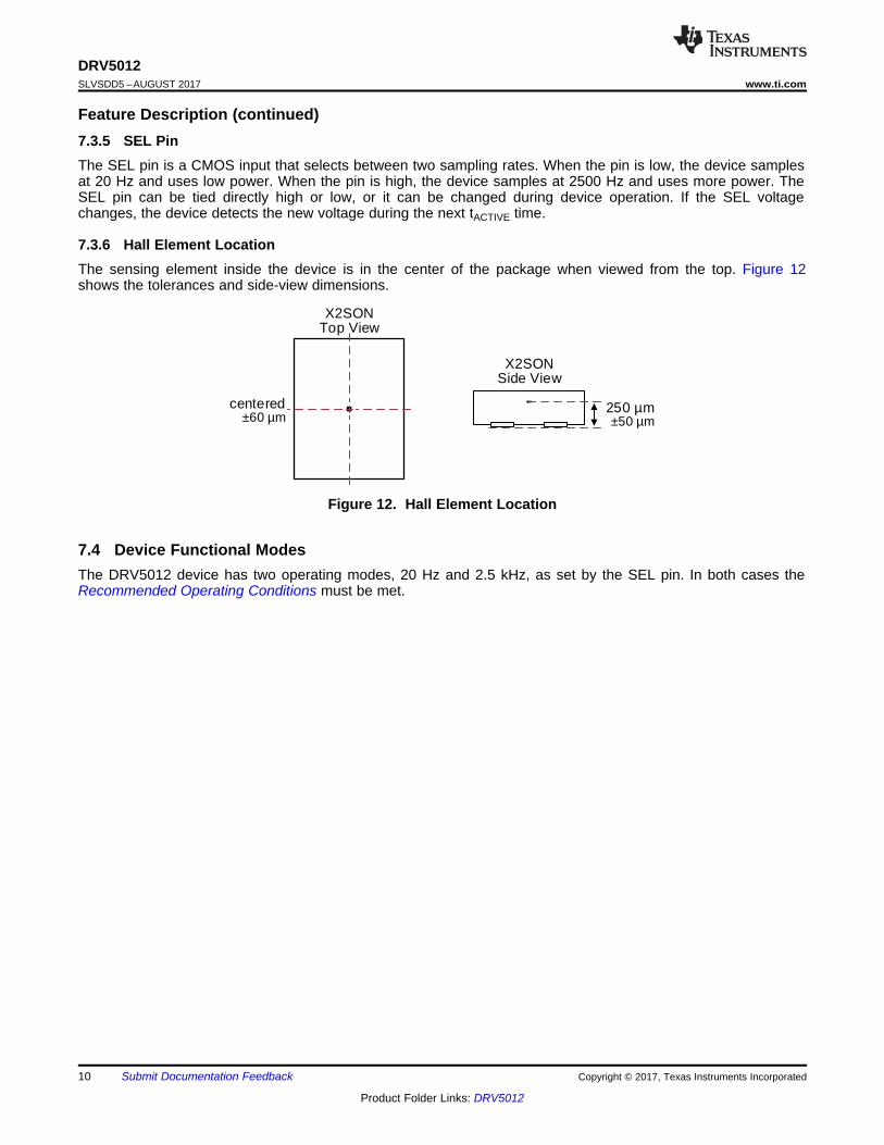
7.3.6 Hall Element LocationThe sensing element inside the device is in the center of the package when viewed from the top. Figure 12shows the tolerances and side-view dimensions.
Figure 12. Hall Element Location
7.4 Device Functional ModesThe DRV5012 device has two operating modes, 20 Hz and 2.5 kHz, as set by the SEL pin. In both cases theRecommended Operating Conditions must be met.

PWM
MicrocontrollerM
GPIOsSEL control
Outputs
GPIOs
VBATVBAT
DRV5012
DRV5012
DRV50126 Gate Drivers& MOSFETs
GPIO
3
Copyright © 2017, Texas Instruments Incorporated
11
DRV5012www.ti.com SLVSDD5 –AUGUST 2017
Product Folder Links: DRV5012
Submit Documentation FeedbackCopyright © 2017, Texas Instruments Incorporated
8 Application and Implementation
NOTEInformation in the following applications sections is not part of the TI componentspecification, and TI does not warrant its accuracy or completeness. TI’s customers areresponsible for determining suitability of components for their purposes. Customers shouldvalidate and test their design implementation to confirm system functionality.
8.1 Application InformationThe DRV5012 device is typically used in rotary applications for brushless DC (BLDC) motor sensors orincremental rotary encoding.
To ensure reliable functionality, the magnet should apply a flux density at the sensor greater than the maximumBOP and less than the minimum BRP thresholds. It is good practice to add additional margin to account formechanical tolerance, temperature effects, and magnet variation.
8.2 Typical Applications
8.2.1 BLDC Motor Sensors Application
Figure 13. BLDC Motor System
8.2.1.1 Design RequirementsFor this design example, use the parameters listed in Table 1.
Table 1. Design ParametersDESIGN PARAMETER EXAMPLE VALUE
Number of motor phases 3Motor RPM 3000
Number of magnet poles on the rotor 6Magnetic material Bonded Neodymium
Peak magnetic flux density at the Hall sensors ±15 mTBattery voltage range (VBAT) 2 to 3.5 V

Hall 1
Hall 2
Hall 3
U
V
W
Phase Voltages
DRV5012 Outputs
Electrical Angle
Mechanical Angle0° 120° 360°240°0° 60° 120°
.
12
DRV5012SLVSDD5 –AUGUST 2017 www.ti.com
Product Folder Links: DRV5012
Submit Documentation Feedback Copyright © 2017, Texas Instruments Incorporated
8.2.1.2 Detailed Design ProcedureThree-phase brushless DC motors often use 3 Hall effect latch devices to measure the electrical angle of therotor and tell the controller how to drive the 3 wires. These wires connect to electromagnet windings, whichgenerate magnetic fields that apply forces to the permanent magnets on the rotor.
The 3 Hall sensors should be spaced across the printed-circuit board (PCB) so that they are 120° electricaldegrees apart. This configuration creates six 3-bit states with equal time duration for each electrical cycle, whichconsists of 1 north and 1 south magnetic pole. From the center of the motor axis, the number of degrees eachsensor should be spaced equals 2 / [number of poles] × 120°. In this design example, 1 sensor is placed at 0°,1 sensor is placed 40° rotated, and 1 sensor is placed 80° rotated. Alternatively, a 3× degree offset can beadded or subtracted to any sensor, meaning the third sensor could alternatively be placed at80° – (3 × 40°) = –40°.
While an ideal BLDC motor would energize the phases at the exact correct times, the DRV5012 deviceintroduces variable lag because of the sampling architecture that achieves low power. An acceptable amount oflag can be measured by the sampling time error as a percentage of the electrical period. This design exampleuses 3000 RPM, which is 50 revolutions per second. Each revolution has 6 poles (3 electrical cycles), so theelectrical frequency is 150 Hz, a period of 6.7 ms. The DRV5012 device in 2.5 kHz mode has a sampling periodof 0.4 ms, which is 6% of the electrical period. Generally, the maximum timing error should be kept under 10% toensure the BLDC motor spins, and timing error can reduce motor efficiency.
When the motor in this example is not driven, the SEL pins of the DRV5012 devices are set to a low voltage, andthe sensor outputs are monitored for changes. If a change occurs, the microcontroller wakes the system into ahigher power state and takes other appropriate action.
8.2.1.3 Application Curve
Figure 14. 3-Phase BLDC Motor Phase Voltages and Hall Signals

VCCControllerDRV5012
VCC
GND
OUT
SEL
DRV5012
VCC
GND
OUT
SEL
N SNS
VCC
VCC
GPIO
GPIO
GPIO
Copyright © 2017, Texas Instruments Incorporated
13
DRV5012www.ti.com SLVSDD5 –AUGUST 2017
Product Folder Links: DRV5012
Submit Documentation FeedbackCopyright © 2017, Texas Instruments Incorporated
8.2.2 Incremental Rotary Encoding Application
Figure 15. Incremental Rotary Encoding System
8.2.2.1 Design RequirementsFor this design example, use the parameters listed in Table 2.
Table 2. Design ParametersDESIGN PARAMETER EXAMPLE VALUE
RPM range 0 to 4000Number of magnet poles 8
Magnetic material FerriteAir gap above the Hall sensors 2.5 mm
Peak magnetic flux density at the sensors ±7 mT
8.2.2.2 Detailed Design ProcedureIncremental encoders are used on knobs, wheels, motors, and flow meters to measure relative rotary movement.By attaching a ring magnet to the rotating component and placing a DRV5012 device nearby, the sensorgenerates voltage pulses as the magnet turns. If directional information is also needed (clockwise versuscounterclockwise), a second DRV5012 device can be added with a phase offset, and then the order of transitionsbetween the two signals describes the direction.
Creating this phase offset requires spacing the two sensors apart on the PCB, and an ideal 90° quadrature offsetis attained when the sensors are separated by half the length of each magnet pole, plus any integer number ofpole lengths. Figure 15 shows this configuration, as the sensors are 1.5 pole lengths apart. One of the sensorschanges its output every 360° / 8 poles / 2 sensors = 22.5° of rotation. For reference, the TI Design TIDA-00480uses a 66-pole magnet with changes every 2.7°.
Because the DRV5012 device periodically samples the magnetic field, there is a limit to the maximum rotationalspeed that can be measured. Generally, the device sampling rate should be faster than 2 times the number ofpoles per second. In this design example, the maximum speed is 4000 RPM, which involves 533 poles persecond. The DRV5012 has a minimum sampling frequency of 1665 Hz (when the SEL pin is high), which isapproximately 3 × 533 poles per second.
In systems where the sensor sampling rate is close to 2 times the number of poles per second, most of thesamples will measure a magnetic field that is significantly lower than the peak value, since the peaks only occurwhen the sensor and pole are perfectly aligned. In this case, margin should be added by applying a strongermagnetic field that has peaks significantly higher than the maximum BOP of the DRV5012 device.

time
Voltage
Sensor 2Sensor 1
14
DRV5012SLVSDD5 –AUGUST 2017 www.ti.com
Product Folder Links: DRV5012
Submit Documentation Feedback Copyright © 2017, Texas Instruments Incorporated
8.2.2.3 Application CurveTwo signals in quadrature provide movement and direction information. Each 2-bit state has unique adjacent2-bit states for clockwise and counterclockwise.
Figure 16. 2-bit Quadrature Output
CORRECT
INCORRECT
N SNS
N
S
N
S
N SNS
N SNS
15
DRV5012www.ti.com SLVSDD5 –AUGUST 2017
Product Folder Links: DRV5012
Submit Documentation FeedbackCopyright © 2017, Texas Instruments Incorporated
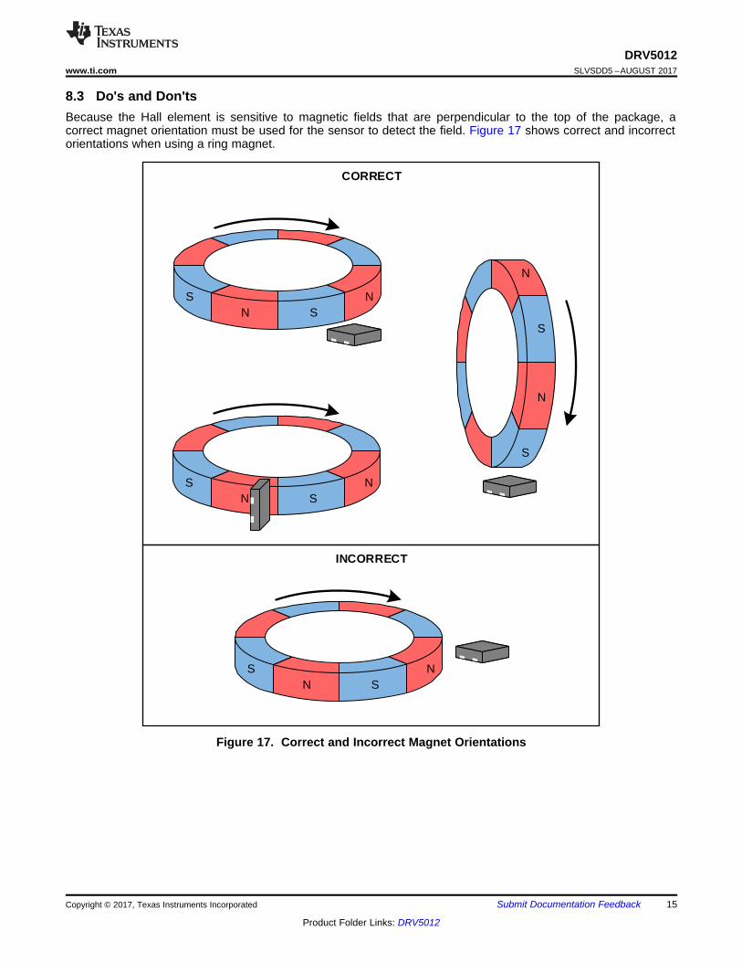
8.3 Do's and Don'tsBecause the Hall element is sensitive to magnetic fields that are perpendicular to the top of the package, acorrect magnet orientation must be used for the sensor to detect the field. Figure 17 shows correct and incorrectorientations when using a ring magnet.
Figure 17. Correct and Incorrect Magnet Orientations

GND OUT
VCC SEL
Thermal Pad
16
DRV5012SLVSDD5 –AUGUST 2017 www.ti.com
Product Folder Links: DRV5012
Submit Documentation Feedback Copyright © 2017, Texas Instruments Incorporated
9 Power Supply RecommendationsThe DRV5012 device is powered from 1.65-V to 5.5-V DC power supplies. A decoupling capacitor close to thedevice must be used to provide local energy with minimal inductance. TI recommends using a ceramic capacitorwith a value of at least 0.1 µF.
10 Layout
10.1 Layout GuidelinesMagnetic fields pass through most nonferromagnetic materials with no significant disturbance. Embedding Halleffect sensors within plastic or aluminum enclosures and sensing magnets on the outside is common practice.Magnetic fields also easily pass through most PCBs, which makes placing the magnet on the opposite sidepossible.
10.2 Layout Example
Figure 18. Layout Example

17
DRV5012www.ti.com SLVSDD5 –AUGUST 2017
Product Folder Links: DRV5012
Submit Documentation FeedbackCopyright © 2017, Texas Instruments Incorporated
11 Device and Documentation Support
11.1 Device Support
11.1.1 Development SupportFor additional design reference, refer to the Automotive Hall Sensor Rotary Encoder TI Design (TIDA-00480).
11.2 Receiving Notification of Documentation UpdatesTo receive notification of documentation updates, navigate to the device product folder on ti.com. In the upperright corner, click on Alert me to register and receive a weekly digest of any product information that haschanged. For change details, review the revision history included in any revised document.
11.3 Community ResourcesThe following links connect to TI community resources. Linked contents are provided "AS IS" by the respectivecontributors. They do not constitute TI specifications and do not necessarily reflect TI's views; see TI's Terms ofUse.
TI E2E™ Online Community TI's Engineer-to-Engineer (E2E) Community. Created to foster collaborationamong engineers. At e2e.ti.com, you can ask questions, share knowledge, explore ideas and helpsolve problems with fellow engineers.
Design Support TI's Design Support Quickly find helpful E2E forums along with design support tools andcontact information for technical support.
11.4 TrademarksE2E is a trademark of Texas Instruments.All other trademarks are the property of their respective owners.
11.5 Electrostatic Discharge CautionThese devices have limited built-in ESD protection. The leads should be shorted together or the device placed in conductive foamduring storage or handling to prevent electrostatic damage to the MOS gates.
11.6 GlossarySLYZ022 — TI Glossary.
This glossary lists and explains terms, acronyms, and definitions.
12 Mechanical, Packaging, and Orderable InformationThe following pages include mechanical, packaging, and orderable information. This information is the mostcurrent data available for the designated devices. This data is subject to change without notice and revision ofthis document. For browser-based versions of this data sheet, refer to the left-hand navigation.

PACKAGE OPTION ADDENDUM
www.ti.com 31-Aug-2017
Addendum-Page 1
PACKAGING INFORMATION
Orderable Device Status(1)
Package Type PackageDrawing
Pins PackageQty
Eco Plan(2)
Lead/Ball Finish(6)
MSL Peak Temp(3)
Op Temp (°C) Device Marking(4/5)
Samples
DRV5012AEDMRR ACTIVE X2SON DMR 4 3000 Green (RoHS& no Sb/Br)
CU SN Level-1-260C-UNLIM -40 to 85 2AE
DRV5012AEDMRT ACTIVE X2SON DMR 4 250 Green (RoHS& no Sb/Br)
CU SN Level-1-260C-UNLIM -40 to 85 2AE
(1) The marketing status values are defined as follows:ACTIVE: Product device recommended for new designs.LIFEBUY: TI has announced that the device will be discontinued, and a lifetime-buy period is in effect.NRND: Not recommended for new designs. Device is in production to support existing customers, but TI does not recommend using this part in a new design.PREVIEW: Device has been announced but is not in production. Samples may or may not be available.OBSOLETE: TI has discontinued the production of the device.
(2) RoHS: TI defines "RoHS" to mean semiconductor products that are compliant with the current EU RoHS requirements for all 10 RoHS substances, including the requirement that RoHS substancedo not exceed 0.1% by weight in homogeneous materials. Where designed to be soldered at high temperatures, "RoHS" products are suitable for use in specified lead-free processes. TI mayreference these types of products as "Pb-Free".RoHS Exempt: TI defines "RoHS Exempt" to mean products that contain lead but are compliant with EU RoHS pursuant to a specific EU RoHS exemption.Green: TI defines "Green" to mean the content of Chlorine (Cl) and Bromine (Br) based flame retardants meet JS709B low halogen requirements of <=1000ppm threshold. Antimony trioxide basedflame retardants must also meet the <=1000ppm threshold requirement.
(3) MSL, Peak Temp. - The Moisture Sensitivity Level rating according to the JEDEC industry standard classifications, and peak solder temperature.
(4) There may be additional marking, which relates to the logo, the lot trace code information, or the environmental category on the device.
(5) Multiple Device Markings will be inside parentheses. Only one Device Marking contained in parentheses and separated by a "~" will appear on a device. If a line is indented then it is a continuationof the previous line and the two combined represent the entire Device Marking for that device.
(6) Lead/Ball Finish - Orderable Devices may have multiple material finish options. Finish options are separated by a vertical ruled line. Lead/Ball Finish values may wrap to two lines if the finishvalue exceeds the maximum column width.
Important Information and Disclaimer:The information provided on this page represents TI's knowledge and belief as of the date that it is provided. TI bases its knowledge and belief on informationprovided by third parties, and makes no representation or warranty as to the accuracy of such information. Efforts are underway to better integrate information from third parties. TI has taken andcontinues to take reasonable steps to provide representative and accurate information but may not have conducted destructive testing or chemical analysis on incoming materials and chemicals.TI and TI suppliers consider certain information to be proprietary, and thus CAS numbers and other limited information may not be available for release.
In no event shall TI's liability arising out of such information exceed the total purchase price of the TI part(s) at issue in this document sold by TI to Customer on an annual basis.

PACKAGE OPTION ADDENDUM
www.ti.com 31-Aug-2017
Addendum-Page 2

TAPE AND REEL INFORMATION
*All dimensions are nominal
Device PackageType
PackageDrawing
Pins SPQ ReelDiameter
(mm)
ReelWidth
W1 (mm)
A0(mm)
B0(mm)
K0(mm)
P1(mm)
W(mm)
Pin1Quadrant
DRV5012AEDMRR X2SON DMR 4 3000 179.0 8.4 1.27 1.57 0.5 4.0 8.0 Q1
PACKAGE MATERIALS INFORMATION
www.ti.com 3-Nov-2017
Pack Materials-Page 1
*All dimensions are nominal
Device Package Type Package Drawing Pins SPQ Length (mm) Width (mm) Height (mm)
DRV5012AEDMRR X2SON DMR 4 3000 203.0 203.0 35.0
PACKAGE MATERIALS INFORMATION
www.ti.com 3-Nov-2017
Pack Materials-Page 2

www.ti.com
PACKAGE OUTLINE
C
4X 0.270.17
0.8±0.05
4X 0.250.15
0.6±0.05
0.050.00
0.4 MAX
2X 0.5
A
1.451.35
B 1.151.05
X2SON - 0.4 mm max heightDMR0004APLASTIC SMALL OUTLINE - NO LEAD
4222825/A 03/2016
PIN 1 INDEX AREA
SEATING PLANE
0.08 C
1
2 3
4
(OPTIONAL)PIN 1 ID
0.1 C B A0.05 C
EXPOSEDTHERMAL PAD
5
SYMM
SYMM
NOTES: 1. All linear dimensions are in millimeters. Any dimensions in parenthesis are for reference only. Dimensioning and tolerancing per ASME Y14.5M. 2. This drawing is subject to change without notice. 3. The package thermal pad must be soldered to the printed circuit board for thermal and mechanical performance.
SCALE 9.000

www.ti.com
EXAMPLE BOARD LAYOUT
0.05 MINALL AROUND
0.05 MAXALL AROUND
(0.6) (1.4)
4X (0.22)
(0.8)
( ) VIA0.2
4X (0.4)
(R ) TYP0.05
2X (0.5)
X2SON - 0.4 mm max heightDMR0004APLASTIC SMALL OUTLINE - NO LEAD
4222825/A 03/2016
SYMM
1
2 3
4
SYMM
LAND PATTERN EXAMPLESCALE:35X
5
NOTES: (continued) 4. This package is designed to be soldered to a thermal pad on the board. For more information, see Texas Instruments literature number SLUA271 (www.ti.com/lit/slua271).5. Vias are optional depending on application, refer to device data sheet. If all or some are implemented, recommended via locations are shown. It is recommended that vias under paste be filled, plugged or tented.
SOLDER MASKOPENING
SOLDER MASKMETAL UNDER
SOLDER MASKDEFINED
METAL
SOLDER MASKOPENING
SOLDER MASK DETAILS
NON SOLDER MASKDEFINED
(PREFERRED)

www.ti.com
EXAMPLE STENCIL DESIGN
4X (0.22)
4X (0.4)
(1.4)
(0.76)
(0.57)
(R ) TYP0.05
2X (0.5)
X2SON - 0.4 mm max heightDMR0004APLASTIC SMALL OUTLINE - NO LEAD
4222825/A 03/2016
NOTES: (continued) 6. Laser cutting apertures with trapezoidal walls and rounded corners may offer better paste release. IPC-7525 may have alternate design recommendations.
SOLDER PASTE EXAMPLEBASED ON 0.1 mm THICK STENCIL
EXPOSED PAD 5:
90% PRINTED SOLDER COVERAGE BY AREASCALE:50X
SYMM
1
2 3
4
SYMM
METALTYP
5

IMPORTANT NOTICE
Texas Instruments Incorporated (TI) reserves the right to make corrections, enhancements, improvements and other changes to itssemiconductor products and services per JESD46, latest issue, and to discontinue any product or service per JESD48, latest issue. Buyersshould obtain the latest relevant information before placing orders and should verify that such information is current and complete.TI’s published terms of sale for semiconductor products (http://www.ti.com/sc/docs/stdterms.htm) apply to the sale of packaged integratedcircuit products that TI has qualified and released to market. Additional terms may apply to the use or sale of other types of TI products andservices.Reproduction of significant portions of TI information in TI data sheets is permissible only if reproduction is without alteration and isaccompanied by all associated warranties, conditions, limitations, and notices. TI is not responsible or liable for such reproduceddocumentation. Information of third parties may be subject to additional restrictions. Resale of TI products or services with statementsdifferent from or beyond the parameters stated by TI for that product or service voids all express and any implied warranties for theassociated TI product or service and is an unfair and deceptive business practice. TI is not responsible or liable for any such statements.Buyers and others who are developing systems that incorporate TI products (collectively, “Designers”) understand and agree that Designersremain responsible for using their independent analysis, evaluation and judgment in designing their applications and that Designers havefull and exclusive responsibility to assure the safety of Designers' applications and compliance of their applications (and of all TI productsused in or for Designers’ applications) with all applicable regulations, laws and other applicable requirements. Designer represents that, withrespect to their applications, Designer has all the necessary expertise to create and implement safeguards that (1) anticipate dangerousconsequences of failures, (2) monitor failures and their consequences, and (3) lessen the likelihood of failures that might cause harm andtake appropriate actions. Designer agrees that prior to using or distributing any applications that include TI products, Designer willthoroughly test such applications and the functionality of such TI products as used in such applications.TI’s provision of technical, application or other design advice, quality characterization, reliability data or other services or information,including, but not limited to, reference designs and materials relating to evaluation modules, (collectively, “TI Resources”) are intended toassist designers who are developing applications that incorporate TI products; by downloading, accessing or using TI Resources in anyway, Designer (individually or, if Designer is acting on behalf of a company, Designer’s company) agrees to use any particular TI Resourcesolely for this purpose and subject to the terms of this Notice.TI’s provision of TI Resources does not expand or otherwise alter TI’s applicable published warranties or warranty disclaimers for TIproducts, and no additional obligations or liabilities arise from TI providing such TI Resources. TI reserves the right to make corrections,enhancements, improvements and other changes to its TI Resources. TI has not conducted any testing other than that specificallydescribed in the published documentation for a particular TI Resource.Designer is authorized to use, copy and modify any individual TI Resource only in connection with the development of applications thatinclude the TI product(s) identified in such TI Resource. NO OTHER LICENSE, EXPRESS OR IMPLIED, BY ESTOPPEL OR OTHERWISETO ANY OTHER TI INTELLECTUAL PROPERTY RIGHT, AND NO LICENSE TO ANY TECHNOLOGY OR INTELLECTUAL PROPERTYRIGHT OF TI OR ANY THIRD PARTY IS GRANTED HEREIN, including but not limited to any patent right, copyright, mask work right, orother intellectual property right relating to any combination, machine, or process in which TI products or services are used. Informationregarding or referencing third-party products or services does not constitute a license to use such products or services, or a warranty orendorsement thereof. Use of TI Resources may require a license from a third party under the patents or other intellectual property of thethird party, or a license from TI under the patents or other intellectual property of TI.TI RESOURCES ARE PROVIDED “AS IS” AND WITH ALL FAULTS. TI DISCLAIMS ALL OTHER WARRANTIES ORREPRESENTATIONS, EXPRESS OR IMPLIED, REGARDING RESOURCES OR USE THEREOF, INCLUDING BUT NOT LIMITED TOACCURACY OR COMPLETENESS, TITLE, ANY EPIDEMIC FAILURE WARRANTY AND ANY IMPLIED WARRANTIES OFMERCHANTABILITY, FITNESS FOR A PARTICULAR PURPOSE, AND NON-INFRINGEMENT OF ANY THIRD PARTY INTELLECTUALPROPERTY RIGHTS. TI SHALL NOT BE LIABLE FOR AND SHALL NOT DEFEND OR INDEMNIFY DESIGNER AGAINST ANY CLAIM,INCLUDING BUT NOT LIMITED TO ANY INFRINGEMENT CLAIM THAT RELATES TO OR IS BASED ON ANY COMBINATION OFPRODUCTS EVEN IF DESCRIBED IN TI RESOURCES OR OTHERWISE. IN NO EVENT SHALL TI BE LIABLE FOR ANY ACTUAL,DIRECT, SPECIAL, COLLATERAL, INDIRECT, PUNITIVE, INCIDENTAL, CONSEQUENTIAL OR EXEMPLARY DAMAGES INCONNECTION WITH OR ARISING OUT OF TI RESOURCES OR USE THEREOF, AND REGARDLESS OF WHETHER TI HAS BEENADVISED OF THE POSSIBILITY OF SUCH DAMAGES.Unless TI has explicitly designated an individual product as meeting the requirements of a particular industry standard (e.g., ISO/TS 16949and ISO 26262), TI is not responsible for any failure to meet such industry standard requirements.Where TI specifically promotes products as facilitating functional safety or as compliant with industry functional safety standards, suchproducts are intended to help enable customers to design and create their own applications that meet applicable functional safety standardsand requirements. Using products in an application does not by itself establish any safety features in the application. Designers mustensure compliance with safety-related requirements and standards applicable to their applications. Designer may not use any TI products inlife-critical medical equipment unless authorized officers of the parties have executed a special contract specifically governing such use.Life-critical medical equipment is medical equipment where failure of such equipment would cause serious bodily injury or death (e.g., lifesupport, pacemakers, defibrillators, heart pumps, neurostimulators, and implantables). Such equipment includes, without limitation, allmedical devices identified by the U.S. Food and Drug Administration as Class III devices and equivalent classifications outside the U.S.TI may expressly designate certain products as completing a particular qualification (e.g., Q100, Military Grade, or Enhanced Product).Designers agree that it has the necessary expertise to select the product with the appropriate qualification designation for their applicationsand that proper product selection is at Designers’ own risk. Designers are solely responsible for compliance with all legal and regulatoryrequirements in connection with such selection.Designer will fully indemnify TI and its representatives against any damages, costs, losses, and/or liabilities arising out of Designer’s non-compliance with the terms and provisions of this Notice.
Mailing Address: Texas Instruments, Post Office Box 655303, Dallas, Texas 75265Copyright © 2017, Texas Instruments Incorporated