drv2700 high voltage driver with integrated boost ... - … · drv2700 slos861b –march...
TRANSCRIPT

Gain OUT±
GND
IN+
Boost Controller
OUT+
PUMP
R(REXT)
C(VDD)
L1
VDD SW
REXT
IN±
C(IN)
C(PUMP)
C(IN)
BST
C(BOOST)
R(FB1)
R(FB2)
FB
PVDD
Piezo Element
EN
GAIN0
GAIN1
Charge Pump
Thermal Shutdown
Product
Folder
Sample &Buy
Technical
Documents
Tools &
Software
Support &Community
DRV2700SLOS861B –MARCH 2015–REVISED APRIL 2015
DRV2700 Industrial Piezo Driver With Integrated Boost Converter1 Features 3 Description
The DRV2700 device is a single-chip piezo driver1• 100-V Boost or 1-kV Flyback Configuration
with an integrated 105-V boost switch, integrated• ±100-V Piezo Driver in Boost + Amplifier power diode, and integrated fully-differential amplifier.Configuration This versatile device is capable of driving both high-– 4 GPIO-Adjustable Gains voltage and low-voltage piezoelectric loads. The input
signal can be either differential or single-ended and– Differential or Single-Ended OutputAC or DC coupled. The DRV2700 device supports– Low-Voltage Control four GPIO-controlled gains: 28.8 dB, 34.8 dB, 38.4
– AC and DC Output Control dB, and 40.7 dB.• 0 to 1-kV Piezo Driver in Flyback Configuration The boost voltage is set using two external resistors.
– Low-Voltage Control The boost current-limit is programmable through theR(REXT) resistor. The boost converter architecture– AC and DC Output Controldoes not allow the demand on the supply current to• Integrated Boost or Flyback Converter exceed the limit set by the R(REXT) resistor which
– Adjustable Current-Limit allows the user to optimize the DRV2700 circuit for agiven inductor based on the desired performance– Integrated Power FET and Dioderequirements. Additionally, this boost converter is• Fast Startup Time of 1.5 ms based on a hysteretic architecture to minimize
• Wide Supply-Voltage Range of 3 to 5.5 V switching losses and therefore increase efficiency.• 4-mm × 4-mm × 0.9-mm VQFN package A typical startup time of 1.5 ms makes the DRV2700• 1.8-V Compatible Digital Pins device an ideal piezo driver for coming out of sleep
quickly. Thermal overload protection prevents the• Thermal Protectiondevice from damage when overdriven.
2 ApplicationsDevice Information(1)
• Piezo Positioning Actuators DEVICE NAME PACKAGE BODY SIZE (NOM)• Piezo Sounder Driver DRV2700 VQFN (20) 4.00 mm × 4.00 mm• Piezo Inkjet Printer
(1) For all available packages, see the orderable addendum at• Piezo Transducers the end of the datasheet.
• Piezoelectric Micropumps
4 Boost + Amplifier Configuration
1
An IMPORTANT NOTICE at the end of this data sheet addresses availability, warranty, changes, use in safety-critical applications,intellectual property matters and other important disclaimers. PRODUCTION DATA.

DRV2700SLOS861B –MARCH 2015–REVISED APRIL 2015 www.ti.com
Table of Contents8.3 Feature Description................................................. 111 Features .................................................................. 18.4 Device Functional Modes ....................................... 122 Applications ........................................................... 1
9 Application and Implementation ........................ 133 Description ............................................................. 19.1 Application Information .......................................... 134 Boost + Amplifier Configuration .......................... 19.2 Typical Applications ................................................ 135 Revision History..................................................... 29.3 System Example ..................................................... 266 Pin Configuration and Functions ......................... 3
10 Power Supply Recommendations ..................... 277 Specifications......................................................... 411 Layout................................................................... 277.1 Absolute Maximum Ratings ..................................... 4
11.1 Layout Guidelines ................................................. 277.2 ESD Ratings.............................................................. 411.2 Layout Example .................................................... 287.3 Recommended Operating Conditions....................... 4
12 Device and Documentation Support ................. 297.4 Thermal Information .................................................. 412.1 Documentation Support ........................................ 297.5 Electrical Characteristics........................................... 512.2 Trademarks ........................................................... 297.6 Switching Characteristics .......................................... 512.3 Electrostatic Discharge Caution............................ 297.7 Typical characteristics............................................... 612.4 Glossary ................................................................ 298 Detailed Description ............................................ 10
13 Mechanical, Packaging, and Orderable8.1 Overview ................................................................. 10Information ........................................................... 298.2 Functional Block Diagram ....................................... 10
5 Revision History
Changes from Revision A (March 2015) to Revision B Page
• Changed "minimum switching frequency" to "miminum startup switching frequency" in Switching Characteristics ............. 5
Changes from Original (March 2015) to Revision A Page
• Released full version of data sheet ....................................................................................................................................... 1
2 Submit Documentation Feedback Copyright © 2015, Texas Instruments Incorporated
Product Folder Links: DRV2700
EN
20
IN+
17
IN±
16
GA
IN0
18
GA
IN1
19
REXT15
OUT±14
BST11
PVDD12
OUT+13
PUMP 1
VDD 2
GND 5
GND 4
FB 3
GN
D6
NC
9
BS
T10
SW
8
SW
7
Thermal Pad
DRV2700www.ti.com SLOS861B –MARCH 2015–REVISED APRIL 2015
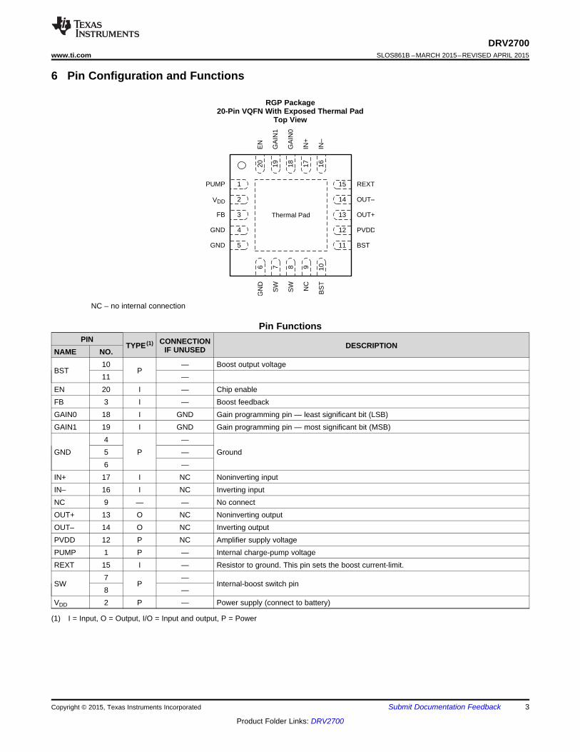
6 Pin Configuration and Functions
RGP Package20-Pin VQFN With Exposed Thermal Pad
Top View
NC – no internal connection
Pin FunctionsPIN CONNECTIONTYPE (1) DESCRIPTIONIF UNUSEDNAME NO.
10 — Boost output voltageBST P
11 —EN 20 I — Chip enableFB 3 I — Boost feedbackGAIN0 18 I GND Gain programming pin — least significant bit (LSB)GAIN1 19 I GND Gain programming pin — most significant bit (MSB)
4 —GND 5 P — Ground
6 —IN+ 17 I NC Noninverting inputIN– 16 I NC Inverting inputNC 9 — — No connectOUT+ 13 O NC Noninverting outputOUT– 14 O NC Inverting outputPVDD 12 P NC Amplifier supply voltagePUMP 1 P — Internal charge-pump voltageREXT 15 I — Resistor to ground. This pin sets the boost current-limit.
7 —SW P Internal-boost switch pin
8 —VDD 2 P — Power supply (connect to battery)
(1) I = Input, O = Output, I/O = Input and output, P = Power
Copyright © 2015, Texas Instruments Incorporated Submit Documentation Feedback 3
Product Folder Links: DRV2700

DRV2700SLOS861B –MARCH 2015–REVISED APRIL 2015 www.ti.com
7 Specifications
7.1 Absolute Maximum Ratings (1)
Over operating free-air temperature range (unless otherwise noted)MIN MAX UNIT
Supply voltage VDD –0.3 6 VInput voltage IN+, IN–, EN, GAIN0, GAIN1, FB –0.3 VDD + 0.3 VBoost/Output Voltage PVDD, SW, OUT+, OUT– 120 VLead temperature 1.6 mm (1/16 inch) from case for 10 seconds 260 °COperating free-air temperature, TA –40 85 °COperating junction temperature, TJ –40 150 °CStorage temperature, Tstg –65 150 °C
(1) Stresses beyond those listed under absolute maximum ratings may cause permanent damage to the device. These are stress ratingsonly, and functional operations of the device at these or any other conditions beyond those indicated under recommended operatingconditions is not implied. Exposure to absolute-maximum-rated conditions for extended periods may affect device reliability.
7.2 ESD RatingsVALUE UNIT
Human body model (HBM), per ANSI/ESDA/JEDEC JS-001, all pins ±2500V(ESD) Electrostatic discharge VCharged device model (CDM), per JEDEC specification JESD22-C101, ±1500all pins
7.3 Recommended Operating ConditionsMIN NOM MAX UNIT
VDD Supply voltage VDD 3 5.5 VV(BST) Boost voltage BST 15 105 VVID Differential input voltage IN+, IN– 1.8 (1) VVIL Digital input low voltage EN, GAIN0, GAIN1; VDD = 3.6 V 0.75 VVIH Digital input high voltage EN, GAIN0, GAIN1; VDD = 3.6 V 1.4 VR(REXT) Current-limit control resistor 6 35 kΩL Inductance for boost converter 3.3 µH
(1) Gains are optimized for a 1.8-V peak input
7.4 Thermal InformationRGP (VQFN)THERMAL METRIC (1) UNIT20 PINS
RθJA Junction-to-ambient thermal resistance 33.1RθJC(top) Junction-to-case (top) thermal resistance 30.9RθJB Junction-to-board thermal resistance 8.7
°C/WψJT Junction-to-top characterization parameter 0.4ψJB Junction-to-board characterization parameter 8.7RθJC(bot) Junction-to-case (bottom) thermal resistance 2.5
(1) For more information about traditional and new thermal metrics, see the IC Package Thermal Metrics application report, SPRA953.
4 Submit Documentation Feedback Copyright © 2015, Texas Instruments Incorporated
Product Folder Links: DRV2700

DRV2700www.ti.com SLOS861B –MARCH 2015–REVISED APRIL 2015
7.5 Electrical CharacteristicsTA = 25°C, VOUT(PP) = VOUT+ – VOUT– = 200 V, C(LOAD) = 47 nF, G(AMP) = 40 dB, L = 4.7 µH (unless otherwise noted)
PARAMETER TEST CONDITIONS MIN TYP MAX UNIT|IIL| Digital-input low current EN, GAIN0, GAIN1; VDD = 3.6 V, VI = 0 V 1 µA|IIH| Digital-input high current EN, GAIN0, GAIN1; VDD = 3.6 V, VI = VDD 5 µAIL(sd) Shutdown current VDD = 3.6 V, V(EN) = 0 V 13 µA
VDD = 3.6 V, V(EN) = VDD, V(BST) = 105 V, no signal 24 mAVDD = 3.6 V, V(EN) = VDD, V(BST) = 80 V, no signal 13 mA
IQ Quiescent currentVDD = 3.6 V, V(EN) = VDD, V(BST) = 55 V, no signal 9 mAVDD = 3.6 V, V(EN) = VDD, V(BST) = 30 V, no signal 5 mA
VOS Offset voltage VDD = 3.6 V, V(EN) = 3.6 V 25 mVVDD –CMVR Common-mode voltage VDD = 3.6 V, V(EN) = 3.6 V 0.2 V0.4
Common-mode rejectionCMRR VDD = 3.6 V, V(EN) = 3.6 V 100 dBratioPSRR Power-supply rejection ratio VDD = 3.6 V, V(EN) = 3.6 V 60 dBRI Input impedance All gains, IN+, IN– 100 kΩ
GAIN[1:0] = 00 28.8GAIN[1:0] = 01 34.8
G(AMP) Amplifier gain dBGAIN[1:0] = 10 38.4GAIN[1:0] = 11 40.7GAIN[1:0] = 00, No Load 150GAIN[1:0] = 01, No Load 300
SR Slew rate V/msGAIN[1:0] = 10, No Load 450GAIN[1:0] = 11, No Load 600GAIN[1:0] = 00, VOUT(PP) = 50 V, No Load 20GAIN[1:0] = 01, VOUT(PP) = 100 V, No Load 10
BW Amplifier bandwidth kHzGAIN[1:0] = 10, VOUT(PP) = 150 V, No Load 7.5GAIN[1:0] = 11, VOUT(PP) = 200 V, No Load 5
GBW Gain-bandwidth product VDD = 3.6 V, V(EN) = 3.6 V 550 kHzVn Input Voltage Noise VDD = 3.6 V, V(EN) = 3.6 V 6.5 µV/√Hz
Total harmonic distortionTHD+N ƒ = 300 Hz, VOUT(PP) = 200 V 1%plus noise
7.6 Switching CharacteristicsVDD = 3.6 V, TA = 25°C, VOUT(PP) = VOUT+ – VOUT– = 200 V, C(LOAD) = 47 nF, G(AMP) = 40 dB, L = 4.7 µH (unless otherwisenoted)
PARAMETER TEST CONDITIONS MIN TYP MAX UNITStartup time—time from EN high untilt(start) 1.5 msboost and amplifier are fully enabled
ƒMIN Minimum startup switching frequency 39 kHz
Copyright © 2015, Texas Instruments Incorporated Submit Documentation Feedback 5
Product Folder Links: DRV2700

Time (ms)
BS
TV
oltage
0.0 0.2 0.4 0.6 0.8 1.0 1.2 1.4 1.6 1.8 2.0
0
20
40
60
80
100
120
140EN (in 200-mV scale)
VBST
Supply Voltage (V)
BS
TV
oltage (
V)
3.00 3.25 3.50 3.75 4.00 4.25 4.50 4.75 5.00 5.25 5.50
103
104
105
106
107
108
109
110
No Load
Boost Load Current (mA)
Boo
st E
ffici
ency
(%
)
Boo
st V
olta
ge (
V)
0 5 10 15 20 25 30 35 40 45 50 55 600 0
10 10
20 20
30 30
40 40
50 50
60 60
70 70
80 80
90 90
100 100
110 110
120 120
D003
Boost EfficiencyBoost VoltageOut of Regulation
Boost Load Current (mA)
Boo
st E
ffici
ency
(%
)
Boo
st V
olta
ge (
V)
0 5 10 15 20 25 30 35 40 45 50 55 600 0
10 10
20 20
30 30
40 40
50 50
60 60
70 70
80 80
90 90
100 100
110 110
120 120
D004
Boost EfficiencyBoost VoltageOut of Regulation
Boost Load Current (mA)
Boo
st E
ffici
ency
(%
)
Boo
st V
olta
ge (
V)
0 5 10 15 20 25 30 35 40 45 50 55 600 0
10 10
20 20
30 30
40 40
50 50
60 60
70 70
80 80
90 90
100 100
110 110
120 120
D001
Boost EfficiencyBoost VoltageOut of Regulation
Boost Load Current (mA)
Boo
st E
ffici
ency
(%
)
Boo
st V
olta
ge (
V)
0 5 10 15 20 25 30 35 40 45 50 55 600 0
10 10
20 20
30 30
40 40
50 50
60 60
70 70
80 80
90 90
100 100
110 110
120 120
D002
Boost EfficiencyBoost VoltageOut of Regulation
DRV2700SLOS861B –MARCH 2015–REVISED APRIL 2015 www.ti.com
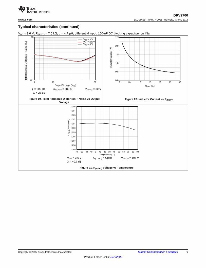
7.7 Typical characteristicsVDD = 3.6 V, R(REXT) = 7.5 kΩ, L = 4.7 µH, differential input, 100-nF DC blocking capacitors on IN±
VDD = 3.6 V C(LOAD) = Open VPVDD = 30 V VDD = 3.6 V C(LOAD) = Open VPVDD = 55 VG = 28.8 dB G = 34.8 dB
Figure 1. Load Current vs Boost Efficiency (%) and Voltage Figure 2. Load Current vs Boost Efficiency (%) and Voltage(V) at VPVDD = 30 V (V) at VPVDD = 55 V
VDD = 3.6 V C(LOAD) = Open VPVDD = 80 V VDD = 3.6 V C(LOAD) = Open VPVDD = 105 VG = 38.4 dB G = 40.7 dB
Figure 3. Load Current vs Boost Efficiency (%) and Voltage Figure 4. Load Current vs Boost Efficiency (%) and Voltage(V) at VPVDD = 80 V (V) at VPVDD = 105 V
G = 40.7 dB C(LOAD) = Open VPVDD = 105 V VDD = 3.6 V C(LOAD) = Open VPVDD = 105 VG = 40.7 dB
Figure 5. Line Regulation at PVDD = 105 V Figure 6. Boost Voltage Startup
6 Submit Documentation Feedback Copyright © 2015, Texas Instruments Incorporated
Product Folder Links: DRV2700

Frequency (Hz)
Outp
ut V
oltage (
V)
PP
20 100 1k 10k 20k
0
50
100
150
200
250
300
No Load
Load = 33 nF
Load = 100 nF
Load = 330 nF
Load = 1 µF
Frequency (Hz)
Outp
ut V
oltage (
V)
PP
20 100 1k 10k 20k
0
50
100
150
200
250
300
350
No Load
Load = 33 nF
Load = 100 nF
Load = 330 nF
Load = 1 µF
Frequency (Hz)
Outp
ut V
oltage (
VP
P)
20 100 1k 10k 20k
0
10
20
30
40
50
60
70
80
90
100
110
No Load
Load = 33 nF
Load = 100 nF
Load = 330 nF
Load = 1 µF
Load = 4.7 µF
Frequency (Hz)
Outp
ut V
oltage (
V)
PP
20 100 1k 10k 20k
0
25
50
75
100
125
150
175
200
No Load
Load = 33 nF
Load = 100 nF
Load = 330 nF
Load = 1 µF
Load = 4.7 µF
Frequency (Hz)
Pow
er
Supply
Reje
ction R
atio (
dB
)
20 100 1k 10k 20k
−90
−80
−70
−60
−50
−40
−30VDD = 3.1 V
VDD = 3.6 V
VDD = 5.5 V
Frequency (Hz)
Com
mon M
ode R
eje
ction R
atio (
dB
)
20 100 1k 10k 20k
−160
−150
−140
−130
−120
−110
−100
−90
−80
−70
−60
No Load
DRV2700www.ti.com SLOS861B –MARCH 2015–REVISED APRIL 2015
Typical characteristics (continued)VDD = 3.6 V, R(REXT) = 7.5 kΩ, L = 4.7 µH, differential input, 100-nF DC blocking capacitors on IN±
G = 40.7 dB C(LOAD) = Open VPVDD = 105 V G = 40.7 dB C(LOAD) = Open VPVDD = 105 V
Figure 7. AC PSRR at VPVDD = 105 V Figure 8. AC CMRR at VPVDD = 105 V
VDD = 3.6 V G = 28.8 dB VPVDD = 30 V VDD = 3.6 V G = 34.8 dB VPVDD = 55 V
Figure 9. Gain Bandwidth at VPVDD = 30 V Figure 10. Gain Bandwidth at VPVDD = 55 V
VDD = 3.6 V G = 38.4 dB VPVDD = 80 V VDD = 3.6 V G = 40.7 dB VPVDD = 105 V
Figure 11. Gain Bandwidth at VPVDD = 80 V Figure 12. Gain Bandwidth at VPVDD = 105 V
Copyright © 2015, Texas Instruments Incorporated Submit Documentation Feedback 7
Product Folder Links: DRV2700

To
tal H
arm
on
ic D
isto
rtio
n +
No
ise
(%
)
0.1
1
10VDD = 3 VVDD = 3.6 VVDD = 5 V
Output Voltage (V )PP
20 100 200
To
tal H
arm
on
ic D
isto
rtio
n +
No
ise
(%
)
0.1
1
10VDD = 3 VVDD = 3.6 VVDD = 5 V
Output Voltage (V )PP
20 100
Output Voltage (V )PP
Su
pp
ly C
urr
en
t (A
)
10
100m
200m
300m
400m
500m
600mVDD = 3 V
VDD = 3.6 V
VDD = 5 V
10 100 200
Time (ms)
Ou
tpu
t V
olta
ge
(V
)
0 2 4 6 8 10 12 14 16 18 20
0
20
40
60
80
100
120
140
160
180
Input (in 200-mV scale)
Load = No Load
Load = 33 nF
Load = 100 nF
Load = 330 nF
Load = 1 µF
Input Voltage (V)
Outp
ut V
oltage (
V)
0.0 0.5 1.0 1.5 2.0 2.5 3.0 3.5 4.0 4.5 5.0
0
20
40
60
80
100
120
140
160V = 105 V(BST)
V(BST) = 80 V
V(BST) = 55 V
V(BST) = 30 V
Input Voltage (V)
Outp
ut V
oltage (
V)
0.0 0.5 1.0 1.5 2.0 2.5 3.0 3.5 4.0 4.5 5.0
0
20
40
60
80
100
120
140
160V(BST) = 105 V
V(BST) = 80 V
V(BST) = 55 V
V(BST) = 30 V
DRV2700SLOS861B –MARCH 2015–REVISED APRIL 2015 www.ti.com
Typical characteristics (continued)VDD = 3.6 V, R(REXT) = 7.5 kΩ, L = 4.7 µH, differential input, 100-nF DC blocking capacitors on IN±
VDD = 3.6 V G = 40.7 dB C(LOAD) = Open VDD = 3.6 V C(LOAD) = OpenG = 28.8 dB at VPVDD = 30 V G = 34.8 dB at VPVDD = 55 VG = 38.4 dB at VPVDD = 80 V G = 40.7 dB at VPVDD = 105 V
Figure 13. Output Linearity Figure 14. Output Linearity with Different Gains
VDD = 3.6 V C(LOAD) = Open VPVDD = 105 V ƒ = 200 Hz C(LOAD) = 47 nF VPVDD = 105 VG = 40.7 dB G = 40 dB
Figure 15. Output Slew Rate Figure 16. Supply Current vs Output Voltage
ƒ = 200 Hz C(LOAD) = 47 nF VPVDD = 105 V ƒ = 200 Hz C(LOAD) = 330 nF VPVDD = 55 VG = 40 dB G = 34 dB
Figure 17. Total Harmonic Distortion + Noise vs Output Figure 18. Total Harmonic Distortion + Noise vs OutputVoltage Voltage
8 Submit Documentation Feedback Copyright © 2015, Texas Instruments Incorporated
Product Folder Links: DRV2700
Temperature (°C)
RV
olta
ge
(V
)(R
EX
T)
−40 −30 −20 −10 0 10 20 30 40 50 60 70 80 90
1.295
1.296
1.297
1.298
1.299
1.300
1.301
1.302
1.303
1.304
1.305
REXT (kΩ)
Ind
ucto
r C
urr
en
t (A
)
0.0
0.5
1.0
1.5
2.0
2.5
105 15 3520 25 30
To
tal H
arm
on
ic D
isto
rtio
n +
No
ise
(%
)
0.1
1
10VDD = 3 VVDD = 3.6 VVDD = 5 V
Output Voltage (V )PP
5 10 50
DRV2700www.ti.com SLOS861B –MARCH 2015–REVISED APRIL 2015
Typical characteristics (continued)VDD = 3.6 V, R(REXT) = 7.5 kΩ, L = 4.7 µH, differential input, 100-nF DC blocking capacitors on IN±
ƒ = 200 Hz C(LOAD) = 680 nF VPVDD = 30 VG = 28 dB
Figure 19. Total Harmonic Distortion + Noise vs Output Figure 20. Inductor Current vs R(REXT)Voltage
VDD = 3.6 V C(LOAD) = Open VPVDD = 105 VG = 40.7 dB
Figure 21. R(REXT) Voltage vs Temperature
Copyright © 2015, Texas Instruments Incorporated Submit Documentation Feedback 9
Product Folder Links: DRV2700

Gain OUT±
GND
IN+
Boost Controller
OUT+
PUMP
R(REXT)
C(VDD)
L1
VDD SW
REXT
IN±
C(IN)
C(PUMP)
C(IN)
BST
C(BOOST)
R(FB1)
R(FB2)
FB
PVDD
Piezo Element
EN
GAIN0
GAIN1
Charge Pump
Thermal Shutdown
DRV2700SLOS861B –MARCH 2015–REVISED APRIL 2015 www.ti.com
8 Detailed Description
8.1 OverviewThe DRV2700 device is a single-chip piezo driver with an integrated 105-V boost switch, integrated power diode,and integrated fully-differential amplifier. This versatile device is capable of driving both high-voltage and low-voltage piezo loads. The input signal can be either differential or single-ended. The DRV2700 device supportsfour GPIO-controlled gains: 28.8 dB, 34.8 dB, 38.4 dB, and 40.7 dB.
The boost voltage is set using two external resistors. The boost current-limit is programmable through the R(REXT)resistor. The boost converter architecture does not allow the demand on the supply current to exceed the limitset by the R(REXT) resistor; therefore, allowing the user to optimize the DRV2700 circuit for a given inductor basedon the desired performance requirements. Additionally, this boost converter is based on a hysteretic architectureto minimize switching losses and therefore increase efficiency.
A typical start-up time of 1.5 ms makes the DRV2700 device an ideal piezo driver for fast responses. Thermaloverload protection prevents the device from damage when overdriven.
8.2 Functional Block Diagram
10 Submit Documentation Feedback Copyright © 2015, Texas Instruments Incorporated
Product Folder Links: DRV2700

DRV2700www.ti.com SLOS861B –MARCH 2015–REVISED APRIL 2015
8.3 Feature Description
8.3.1 Boost Converter and Control LoopThe DRV2700 device creates a boosted supply rail with an integrated DC-DC converter that can go up to 105 V.The switch-mode power supplies have a few different sources of losses. When boosting to very high voltages,the efficiency begins to degrade because of these losses. The DRV2700 device has a hysteretic boost design tominimize switching losses and therefore increase efficiency. A hysteretic controller is a self-oscillation circuit thatregulates the output voltage by keeping the output voltage within a hysteresis window set by a reference voltageregulator and, in this case, the current-limit comparator. Hysteretic converters typically have a larger ripple as atrade off because of the minimized switching. This ripple may vary depending on the output capacitor and load.The power FET and power diode of the boost converter are both integrated within the device to provide therequired switching while minimizing external components. Additionally, the boost voltage output (BST) can beeasily fed into the high-voltage amplifier through the adjacent pin (PVDD) to help minimize routing inductanceand resistance on the board.
8.3.2 High-Voltage AmplifierWhen using the high-voltage amplifier in conjunction with the boost converter, the PVDD pin is located next tothe BST pin to immediately feed the high voltage signal back into the device to power the amplifier. TheDRV2700 device was designed as a differential amplifier. A major benefit of the fully differential amplifier is theimproved common-mode rejection ratio (CMRR) over single-ended input amplifiers. The increased CMRR of thedifferential amplifier reduces sensitivity-to-ground offset that is related noise injection which is important in low-noise systems.
The high-voltage amplifier can be used in a single-ended DC input configuration to provide a DC output on theOUT+ and OUT– pins. The amplifier is very linear across the full voltage range and by using a DAC (digital-to-analog converter) input, the output can be controlled with very good granularity.
Precautions must be taken into thermal concerns of this amplifier because high frequencies, voltage, andcapacitive load combinations can overheat the device. See the Piezo Load Selection section for a generalguideline.
8.3.3 Fast Start-Up (Enable Pin)The DRV2700 device features a fast startup time, which is beneficial for the device come out of shutdown veryquickly. When the EN pin transitions from low to high, the boost supply is turned on, the input capacitor isprecharged to VDD / 2, and the amplifier is enabled in a 1.5 ms (typical) total start-up time.
When AC coupled with larger input capacitors, the input can require additional time to charge up to VDD / 2.Because the charging current on the input capacitors are not ensured to be exactly the same, a non-zerodifferential value can exist during startup. Although this differential output voltage (voltage pop) during startup isnot specified, it should be fairly small and not exceed 2 V.
8.3.4 Gain ControlThe DRV2700 device has programmable gains through the GAIN[1:0] bits. Table 2 lists the gain from IN+ or IN–to OUT+ or OUT–.
Table 1. Programmable GainsGAIN1 GAIN0 GAIN (dB)
0 0 28.80 1 34.81 0 38.41 1 40.7
Copyright © 2015, Texas Instruments Incorporated Submit Documentation Feedback 11
Product Folder Links: DRV2700

DRV2700SLOS861B –MARCH 2015–REVISED APRIL 2015 www.ti.com
The gains are optimized to achieve approximately 50 VPP, 100 VPP, 150 VPP, or 200 VPP at the output withoutclipping from a 1.8-V peak source of a single-ended input signal.
8.3.5 Adjustable Boost VoltageThe output voltage of the integrated boost converter is adjusted by a resistive feedback divider between theboost output voltage (BST) and the feedback pin (FB). The boost voltage should be programmed to a valuegreater than the maximum peak signal voltage that the user expects to create with the DRV2700 amplifier. Lowerboost voltages achieve better system efficiency and therefore should be used when lower amplitude signals areapplied. The minimum boost voltage that is required should be used to save on not only power but also heatdissipation. The maximum allowed boost voltage is 105 V.
8.3.6 Adjustable Boost Current-LimitThe current-limit of the boost switch is adjusted through a resistor to ground placed on the REXT pin. In order toprotect the device, the REXT pin value should remain between 7.5 kΩ and 32.5 kΩ as shown in Figure 20. Toavoid damage to both the inductor and the DRV2700 device, the programmed current-limit must be less than therated saturation limit of the inductor selected by the user. If the combination of the programmed limit and inductorsaturation is not high enough, then the output current of the boost converter is not high enough to regulate theboost output voltage under heavy load conditions. This lower output current causes the boosted rail to sag whichcan possibly cause distortion of the output waveform.
8.3.7 Internal Charge PumpThe DRV2700 device has an integrated charge pump to provide gate drive for internal nodes. The output of thischarge pump is placed on the VPUMP pin. An X5R or X7R storage capacitor with a value of 0.1 µF and avoltage rating of 10 V or greater must be placed at this pin for proper operation. This pin and voltage should notbe used as an external reference or driver.
8.3.8 Thermal ShutdownThe DRV2700 device contains an internal temperature sensor that shuts down both the boost converter and theamplifier when the temperature threshold is exceeded. When the die temperature falls below the threshold, thedevice restarts operation automatically as long as the EN pin is high. Continuous operation of the DRV2700device can cause the device to heat up if proper precautions and operating ranges are not followed. The thermalshutdown function protects the DRV2700 device from damage when overdriven, but usage models which drivethe DRV2700 device into thermal shutdown should always be avoided.
8.4 Device Functional ModesAlthough a high-voltage amplifier can be used in a number of ways, the DRV2700 device was intended for twomain configurations which are boost + amplifier mode and flyback mode.
8.4.1 Boost + Amplifier ModeIn the boost + amplifier mode configuration, the boost converter is used in a boost configuration with a singleinductor. The boost output (BST) is then fed into the high-voltage amplifier (PVDD) to drive the outputs. Thisconfiguration supports the boost converter up to 100 VP and the amplifier to drive 200 VPP or 0 to 100 VP. TheTypical Applications section describes the various implementations of this mode.
8.4.2 Flyback ModeIn the flyback mode configuration, the boost converter is used in a flyback configuration which allows the boostconverter to drive the output to even higher voltages. For example, with a 1:10 turn ratio of the transformer, thetransformer can turn the 100 V on the SW node into 1 kV on the high-voltage output. Figure 37 shows a basiccircuit diagram.
12 Submit Documentation Feedback Copyright © 2015, Texas Instruments Incorporated
Product Folder Links: DRV2700

OUT±
GND
IN+ OUT+
PUMP
R(REXT)
C(VDD)
VDD SW
REXT
IN±
C(IN)
C(PUMP)
C(IN)
BSTC(BOOST)R(FB1)
R(FB2)
FB
PVDD
Piezo Element
EN
GAIN0
GAIN1
DRV2700
Digital Control
VDD
3 to 5.5 V
SignalGenerator
L1
DRV2700www.ti.com SLOS861B –MARCH 2015–REVISED APRIL 2015
9 Application and Implementation
NOTEInformation in the following applications sections is not part of the TI componentspecification, and TI does not warrant its accuracy or completeness. TI’s customers areresponsible for determining suitability of components for their purposes. Customers shouldvalidate and test their design implementation to confirm system functionality.
9.1 Application InformationThe DRV2700 is intended to drive piezo loads. This includes: capacitive loads, piezo sounders, piezo valves,piezo positioning actuators, piezo micropumps, piezo polymers and more.
9.2 Typical Applications
9.2.1 AC-Coupled DAC Input ApplicationThe AC-coupled DAC input circuit shown in Figure 22 is typically used in piezo speaker applications. AC-coupling the DRV2700 device allows the device to only amplify the differential portions of the input whichminimizes the common-mode amplification. Because a digitized AC signal is provided from an external source,such as a microcontroller, an input filter is not required. However, a low-pass filter can be added to minimize theharmonics of the digitized waveform.
Figure 22. AC-Coupled DAC Input
Copyright © 2015, Texas Instruments Incorporated Submit Documentation Feedback 13
Product Folder Links: DRV2700

Frequency (Hz)
Ma
xim
um
Ou
tpu
tD
rive
Vo
lta
ge
(V
)P
0
20
40
60
80
100
120
1 10 100 1k 10k 20k
D007
33 nF100 nF330 nF1000 nF3.3 µF10 µF
DRV2700SLOS861B –MARCH 2015–REVISED APRIL 2015 www.ti.com
Typical Applications (continued)9.2.1.1 Design RequirementsFor this design example, use the parameters listed in Table 2 as the input parameters.
Table 2. Design ParametersDESIGN PARAMETER EXAMPLE VALUE CONSTRAINT
Input voltage 5 V Power sourceOutput voltage ±60 V Piezo load
Maximum output frequency 2 kHz Application
9.2.1.2 Detailed Design ProcedureTo design the entire system follow the design procedure listed in the following sections.
9.2.1.2.1 Piezo Load Selection
Several key specifications must be considered when selecting a piezo actuator such as dimensions, blockingforce, and displacement. However, the key electrical specifications from the driver perspective are voltage ratingand capacitance. The DRV2700 device operating in boost + amplifier mode can drive a variety of capacitances,frequencies, and voltages. However to extend the range in one specification can decrease the range of anotherspecification. For example, if driving audio tones around 1 kHz, a lower capacitance piezo or lower drivingvoltage may be required. Figure 23 shows a general guide to selecting the proper parameters.
Figure 23. Maximum Frequency versus Maximum Voltage for Different Load Capacitances
Based on the design example, if the output voltage must be ±60 VOUT to 2 kHz, then the piezo capacitance mustbe less than 100 nF. For ease of calculation, use a piezo load capacitance of 25 nF.
14 Submit Documentation Feedback Copyright © 2015, Texas Instruments Incorporated
Product Folder Links: DRV2700

(FB1) (FB2)
(FB2) (FB1)
R C
R C
(FB1)BST FB
(FB2)
RV V 1
R
æ ö= +ç ÷
ç ÷è ø
(FB1) (FB1)HV FB OP
(FB2) (FB2)
R RV V 1 V
R R
æ ö æ ö= + -ç ÷ ç ÷
ç ÷ ç ÷è ø è ø
Boost + AmplifierConfiguration
FlybackConfiguration
R(FB1)
R(FB2)
FB
DRV2700
V(BST)
Boost + Amplifier
Configuration
R(FB1)
R(FB2)
FB
DRV2700
C(FB2)
C(FB1)
Flyback Configuration
Op-Amp Output
V(HV)
DRV2700www.ti.com SLOS861B –MARCH 2015–REVISED APRIL 2015
9.2.1.2.2 Programming The Boost Voltage
The boost or flyback output voltage is programmed by an external network as shown in Figure 24.
Figure 24. External Network
Depending on which configuration or mode is used in the system, use Equation 1 to calculate the output voltage.
where• VFB = 1.30 V• VOP = VOL of the operational amplifier (op amp). Typically this can be approximated to 0 V. (1)
The BST pin should be programmed to a value 5-V greater than the largest peak voltage in the system expectedto allow adequate amplifier headroom. Because the programming range for the boost voltage extends to 105 V,the leakage current through the resistor divider becomes significant. TI recommends that the sum of theresistance of R(FB1) and R(FB2) be greater than 500 kΩ.
The flyback mode configuration may require filtering capacitors to go along with the feedback network to increasethe performance at low and high frequencies. Because the charge storage is inversely proportional to thecapacitance, use Equation 2 to calculate the values of the capacitors. In general, select a value of 22 pF forC(FB1).
For this design example, because the value of VPP must be negative, the boost + amplifier configuration must beused. Additionally, because the value of VBST must be 5 V more than VP, VBST is set to 65 V. Using Equation 1,the feedback resistors can be found such that RFB1 = 49 × RFB2. Because the total resistance must be greaterthan 500 kΩ, RFB1= 735 kΩ and RFB2= 15 kΩ.
(2)
NOTEWhen resistor values greater than 1 MΩ are used, PCB contamination causes boostvoltage inaccuracy. Use caution when soldering large resistences, and clean the areawhen finished for best results.
Copyright © 2015, Texas Instruments Incorporated Submit Documentation Feedback 15
Product Folder Links: DRV2700
ref(REXT) (INT)
(LIM)
VR K R
I
æ ö= -ç ÷
ç ÷è ø
DRV2700SLOS861B –MARCH 2015–REVISED APRIL 2015 www.ti.com
9.2.1.2.3 Inductor and Transformer Selection
Inductor selection plays a critical role in the performance of the DRV2700 device. The range of recommendedinductances is from 3.3 to 22 µH. In general, higher inductances within a given manufacturer’s inductor serieshave lower saturation current-limits and lower inductances have higher saturation current-limits. When a largerinductance is selected, the DRV2700 boost converter automatically runs at a lower switching frequency andincurs less switching losses. However, larger values of inductance may have higher ESR which increases theparasitic inductor losses. Because lower values of inductance generally have higher saturation currents,inductors with a lower value are a better choice when attempting to maximize the output current of the boostconverter.
Another factor to consider for transformers is the winding ratio. In general, if a 200-V output is desired then,because the SW node can boost up to 100 V, a transformer of 1:2 (100 V:200 V) is the minimum requiredwinding. However, selecting a slightly higher winding ratio to ensure that the 100 V on the primary side is notsurpassed while trying to boost up to the desired voltage is good design practice.
For this design example, select an inductor of 3.3 µH with a saturation current of 1.5 A.
9.2.1.2.4 Programing the Boost and Flyback Current-Limit
The peak current drawn from the supply through the inductor is set solely by the R(REXT) resistor. This peakcurrent-limit is independent of the selected inductance value, but the inductor is capable of handling thisprogrammed limit. Use Equation 3 to calculate the relationship between R(REXT) and I(LIM).
where• K = 10 500• Vref = 1.35 V• I(LIM) is the desired peak current-limit through the inductor or transformer• R(INT) = 60 Ω (3)
For this design example, because the saturation current is 1.5 A, select 1 A for the I(LIM) value. Using Equation 3,the value of R(EXT) is approximately 14 kΩ.
9.2.1.2.5 Boost Capacitor Selection
The boost output voltage is programmable as high as 105 V. A capacitor with a voltage rating of at least theboost output voltage must be selected. Because ceramic capacitors come in ratings of 100 V or 250 V, a 250-Vrated 100-nF capacitor of the X5R or X7R type is recommended for the 105-V case. The selected capacitorshould have a minimum working capacitance of at least 50 nF. If a smaller ripple on this node is required, then alarger capacitor should be selected. If using a differential output in the boost + amplifier configuration, then theripple is canceled because it is prevelant on both the OUT+ and OUT– pins.
For this design example, a 100-nF capacitor was used.
9.2.1.2.6 Pulldown FET and Resistors
The pulldown FET and resistor are used to help speed up the drain the charge on the high-voltage output.Because the FET must be driven from a comparator, an NMOS FET must be used. During normal operation, theVDS of the NMOS is subject to a any value from approximately 0 V when the FET is on, to the output on theflyback configuration (V(HV)) when the FET is off. Therefore, selecting a FET with a VDS breakdown higher thanthe maximum VHV is required. Additionally, placing a resistor in series with this FET (on the drain side) to limit thecurrent going through the FET is required. This resistor can be sized according to the maximum current allowedper the data sheet of the FET. As an additional measure, a resistor can be placed on the source side to protectthe pulldown FET, such that when current flows through the resistor, it raises the source voltage and therebylowers the VGS and shuts the FET off.
Because this design example is using the boost + amplifier configuration, the pulldown FET and resistors are notrequired.
16 Submit Documentation Feedback Copyright © 2015, Texas Instruments Incorporated
Product Folder Links: DRV2700

DD(Peak)65 V
I 2 2 kHz 25 nF 60 V 408 mA5 V 0.6
= p ´ ´ ´ ´ =
´
BoostDD(Peak) P
DD Boost
VI 2 ƒ C V
V= p ´ ´ ´ ´
´ m
Capacitor(Peak) PI 2 ƒ C V= p ´ ´ ´
DRV2700www.ti.com SLOS861B –MARCH 2015–REVISED APRIL 2015
9.2.1.2.7 Low-Voltage Operation
The lowest gain setting is optimized for 50 VPP with a boost voltage of 30 V. Some applications may not require50 VPP, therefore the designer may choose to program the boost converter as low as 15 V to improve efficiency.When using boost voltages lower than 30 V, consider using a boost capacitor and adjusting the full-scale inputrange First, to reduce boost ripple to an acceptable level, a 50-V rated, 0.22-µF boost capacitor is recommended.Second, the full-scale input range may require adjustment to avoid clipping. Generally, a 1.8-V single-endedPWM signal provides 50 VPP at the lowest gain. For example, if the boost voltage is set to 25 V for a 40 VPP full-scale output signal, the full-scale input range drops to 1.44 V for single-ended PWM inputs. An input voltagedivider may be desired in this case if a 1.8-V I/O is used as a PWM source.
9.2.1.2.8 Current Consumption Calculation
Understanding how the voltage driven onto a piezo actuator relates to the current consumption from the powersupply is useful. Modeling a piezo element as a pure capacitor is reasonably accurate. Use Equation 4 tocalculate the current through a capacitor for an applied sinusoid.
• ƒ is the frequency of the sinusoid in hertz• C is the capacitance of the piezo load in farads• VP is the peak voltage (4)
At the power supply, the actuator current is multiplied by the boost-supply ratio and divided by the efficiency ofthe boost converter as shown in Equation 5.
(5)
Substituting the design example values for the variables into Equation 5 and using a boost efficiency of 60%,yields a typical peak current from the power supply of 408 mA as shown in Equation 6.
(6)
9.2.1.2.9 Input Filter Considerations
Depending on the quality of the source signal provided to the DRV2700 device, an input filter may be required.Some key factors to consider are whether the source is generated from a DAC or from PWM, and the out-of-band content generated. If proper anti-image rejection filtering is used to eliminate image components, the filtercan possibly be eliminated depending on the magnitude of the out-of-band components. If PWM is used, at leasta first-order RC filter is required. The PWM sample rate must be greater than 30 kHz to keep the PWM ripplefrom reaching the piezo element and dissipating unnecessary power. A second-order RC filter may be desirableto further eliminate out-of-band signal content to further drive down power dissipation and eliminate audiblenoise.
For this design example, to ensure higher harmonics of the input signal do not propagate into the device, use alow pass filter with a 3-dB point of 2 kHz. Refer to DRV2700EVM High Voltage Piezo Driver Evaluation Kit,SLOU403, to build this input filter network.
9.2.1.2.10 Output Limiting Factors
Because of the small size of the DRV2700 device, limiting factors must be considered. In each of theapplications, four factors can affect the output. These factors include the following:• Bandwidth of the amplifier• Limited current• Slew rate• Thermal shutdown
Although some of these factors can appear at the same time, each of these factors are shown in the followingfigures to help the designer differentiate between each factor.
Copyright © 2015, Texas Instruments Incorporated Submit Documentation Feedback 17
Product Folder Links: DRV2700
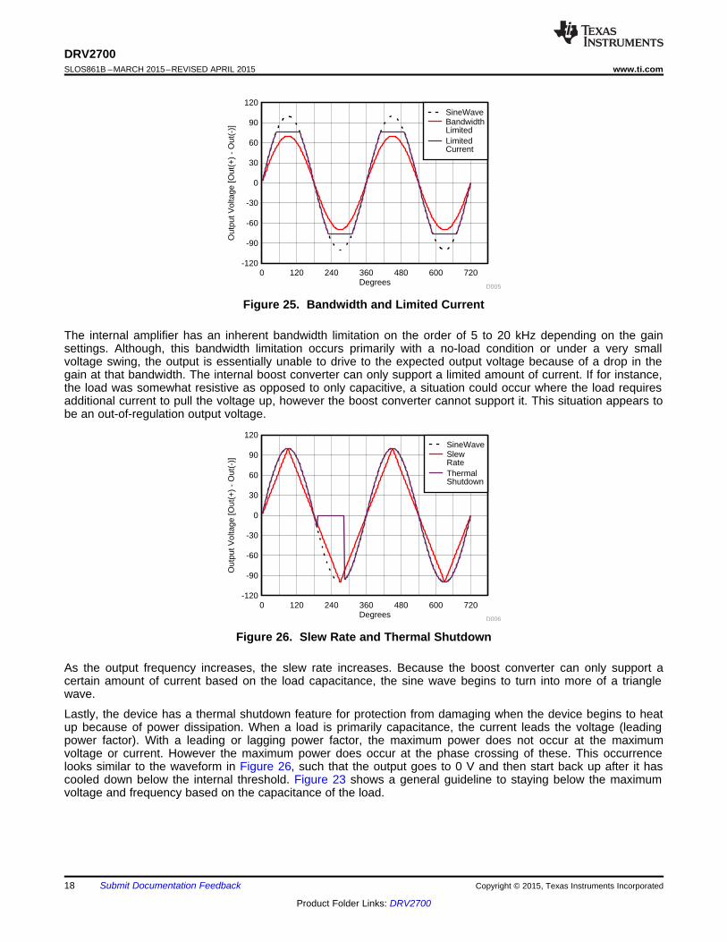
Degrees
Out
put V
olta
ge [O
ut(+
) -
Out
(-)]
0 120 240 360 480 600 720-120
-90
-60
-30
0
30
60
90
120
D006
SineWaveSlewRateThermalShutdown
Degrees
Out
put V
olta
ge [O
ut(+
) -
Out
(-)]
0 120 240 360 480 600 720-120
-90
-60
-30
0
30
60
90
120
D005
SineWaveBandwidthLimitedLimitedCurrent
DRV2700SLOS861B –MARCH 2015–REVISED APRIL 2015 www.ti.com
Figure 25. Bandwidth and Limited Current
The internal amplifier has an inherent bandwidth limitation on the order of 5 to 20 kHz depending on the gainsettings. Although, this bandwidth limitation occurs primarily with a no-load condition or under a very smallvoltage swing, the output is essentially unable to drive to the expected output voltage because of a drop in thegain at that bandwidth. The internal boost converter can only support a limited amount of current. If for instance,the load was somewhat resistive as opposed to only capacitive, a situation could occur where the load requiresadditional current to pull the voltage up, however the boost converter cannot support it. This situation appears tobe an out-of-regulation output voltage.
Figure 26. Slew Rate and Thermal Shutdown
As the output frequency increases, the slew rate increases. Because the boost converter can only support acertain amount of current based on the load capacitance, the sine wave begins to turn into more of a trianglewave.
Lastly, the device has a thermal shutdown feature for protection from damaging when the device begins to heatup because of power dissipation. When a load is primarily capacitance, the current leads the voltage (leadingpower factor). With a leading or lagging power factor, the maximum power does not occur at the maximumvoltage or current. However the maximum power does occur at the phase crossing of these. This occurrencelooks similar to the waveform in Figure 26, such that the output goes to 0 V and then start back up after it hascooled down below the internal threshold. Figure 23 shows a general guideline to staying below the maximumvoltage and frequency based on the capacitance of the load.
18 Submit Documentation Feedback Copyright © 2015, Texas Instruments Incorporated
Product Folder Links: DRV2700
DRV2700www.ti.com SLOS861B –MARCH 2015–REVISED APRIL 2015
9.2.1.2.11 Startup and Shutdown Sequencing
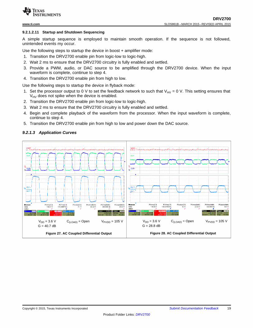
A simple startup sequence is employed to maintain smooth operation. If the sequence is not followed,unintended events my occur.
Use the following steps to startup the device in boost + amplifier mode:1. Transition the DRV2700 enable pin from logic-low to logic-high.2. Wait 2 ms to ensure that the DRV2700 circuitry is fully enabled and settled.3. Provide a PWM, audio, or DAC source to be amplified through the DRV2700 device. When the input
waveform is complete, continue to step 4.4. Transition the DRV2700 enable pin from high to low.
Use the following steps to startup the device in flyback mode:1. Set the processor output to 0 V to set the feedback network to such that VHV = 0 V. This setting ensures that
VHV does not spike when the device is enabled.2. Transition the DRV2700 enable pin from logic-low to logic-high.3. Wait 2 ms to ensure that the DRV2700 circuitry is fully enabled and settled.4. Begin and complete playback of the waveform from the processor. When the input waveform is complete,
continue to step 4.5. Transition the DRV2700 enable pin from high to low and power down the DAC source.
9.2.1.3 Application Curves
VDD = 3.6 V C(LOAD) = Open VPVDD = 105 VVDD = 3.6 V C(LOAD) = Open VPVDD = 105 VG = 28.8 dBG = 40.7 dB
Figure 28. AC Coupled Differential OutputFigure 27. AC Coupled Differential Output
Copyright © 2015, Texas Instruments Incorporated Submit Documentation Feedback 19
Product Folder Links: DRV2700

DRV2700SLOS861B –MARCH 2015–REVISED APRIL 2015 www.ti.com
VDD = 3.6 V C(LOAD) = Open VPVDD = 105 V VDD = 5 V C(LOAD) = 22 nF VHV = 0 to 500 VG = 28.8 dB
Figure 29. DC Coupled Differential Output Figure 30. High Voltage Mode with FET Pulldown
VDD = 5 V C(LOAD) = 22 nF VHV = 0 to 500 V VDD = 5 V C(LOAD) = 22 nF VHV = 0 to 500 V
Figure 31. High Voltage Mode without FET Pulldown Figure 32. High Voltage Mode Arbitrary Waveform
20 Submit Documentation Feedback Copyright © 2015, Texas Instruments Incorporated
Product Folder Links: DRV2700

OUT±
GND
IN+ OUT+
PUMP
R(REXT)
C(VDD)
L1
VDD SW
REXT
IN±
C(IN)
C(PUMP)
C(IN)
BST C(BOOST)R(FB1)
R(FB2)
FB
PVDD
Piezo Element
EN
GAIN0
GAIN1
DRV2700
Digital Control
VDD
3 to 5.5 V
ProcessorR(LPF1)
C(LPF1)
DRV2700www.ti.com SLOS861B –MARCH 2015–REVISED APRIL 2015
9.2.2 Filtered AC Coupled Single-Ended PWM Input ApplicationThe AC coupled single-ended PWM input is very similar to the application described in the AC-Coupled DACInput Application section, however because the input is a true PWM signal, a low-pass filter is highlyrecommended. Typically, a low cutoff frequency is desired to ensure the higher frequencies have beenattenuated and are not amplified.
Figure 33. Filtered AC Coupled Single-Ended PWM Input
Copyright © 2015, Texas Instruments Incorporated Submit Documentation Feedback 21
Product Folder Links: DRV2700

OUT±
GND
IN+ OUT+
PUMP
R(REXT)
C(VDD)
L1
VDD SW
REXT
IN±
C(PUMP)
BST C(BOOST)R(FB1)
R(FB2)
FB
PVDD
Piezo Element
EN
GAIN0
GAIN1
DRV2700
Digital Control
VDD
3 to 5.5 V
R(LPF1)
C(LPF1)
R(LPF2)
C(LPF2)
Processor
DRV2700SLOS861B –MARCH 2015–REVISED APRIL 2015 www.ti.com
9.2.3 DC-Coupled DAC Input ApplicationThe DC-coupled DAC input is used in applications when the user might need to drive the output at a constantDC level. A typical application for th the DC-coupled DAC input is for piezo pneumatic valves. A benefit to thisapplication circuit is that all of the inputs, including power, are at a very low voltage while keeping the high-voltage piezo load separated. This feature allows easy implementation into systems and to help separate orisolate the high voltages loads from the critical controls.
Piezoelectric materials have a certain voltage that debias the piezo phenomenon. To prevent this debiasing fromoccurring, limit the input using a controlled input signal. As a backup measure, place a Zener diode to restrict theinput.
Figure 34. DC-Coupled DAC Input
22 Submit Documentation Feedback Copyright © 2015, Texas Instruments Incorporated
Product Folder Links: DRV2700
OUT±
GND
IN+ OUT+
PUMP
R(REXT)
C(VDD)
VDD SW
REXT
IN±
C(PUMP)
BST C(BOOST)
R(FB1)
R(FB2)
FB
PVDD
Piezo Element
EN
GAIN0
GAIN1
DRV2700
VDD
3 to 5.5 V
R(DIFF2)
R(DIFF3)
R(DIFF1)
Vref
L1
DRV2700www.ti.com SLOS861B –MARCH 2015–REVISED APRIL 2015
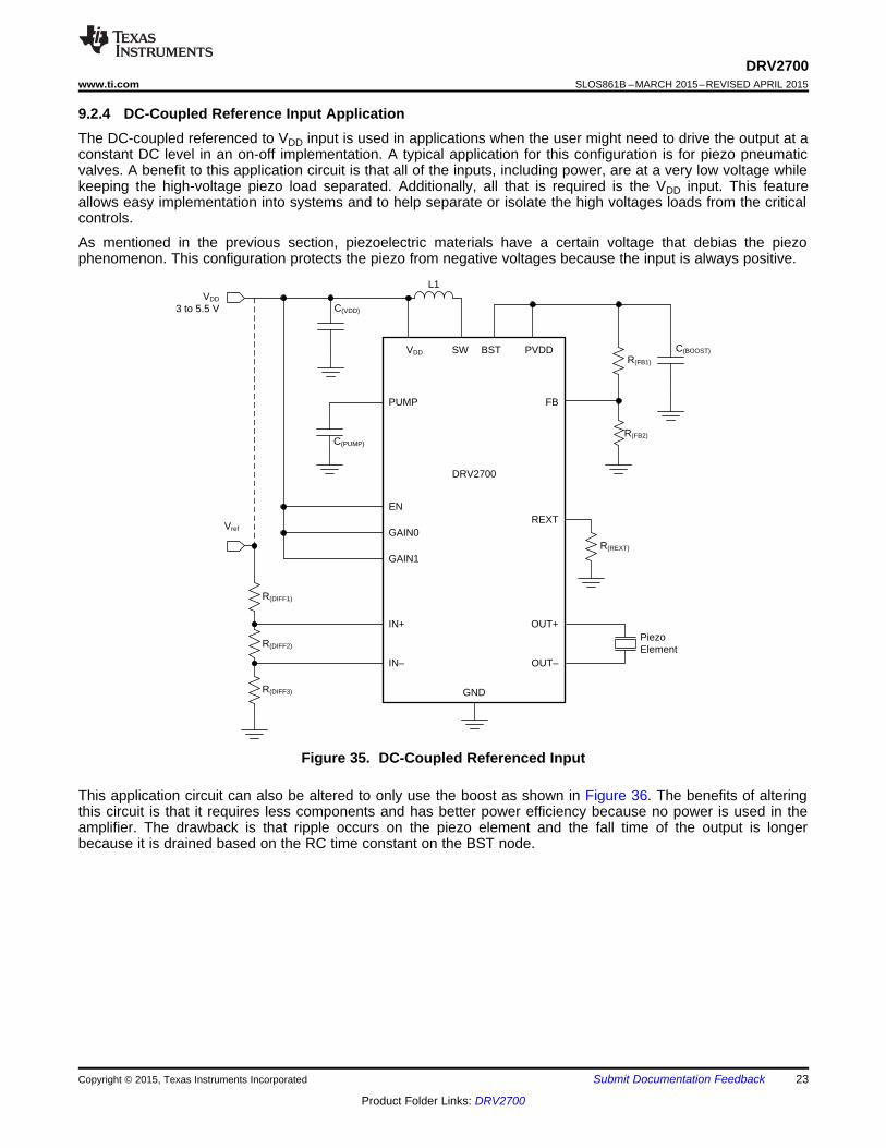
9.2.4 DC-Coupled Reference Input ApplicationThe DC-coupled referenced to VDD input is used in applications when the user might need to drive the output at aconstant DC level in an on-off implementation. A typical application for this configuration is for piezo pneumaticvalves. A benefit to this application circuit is that all of the inputs, including power, are at a very low voltage whilekeeping the high-voltage piezo load separated. Additionally, all that is required is the VDD input. This featureallows easy implementation into systems and to help separate or isolate the high voltages loads from the criticalcontrols.
As mentioned in the previous section, piezoelectric materials have a certain voltage that debias the piezophenomenon. This configuration protects the piezo from negative voltages because the input is always positive.
Figure 35. DC-Coupled Referenced Input
This application circuit can also be altered to only use the boost as shown in Figure 36. The benefits of alteringthis circuit is that it requires less components and has better power efficiency because no power is used in theamplifier. The drawback is that ripple occurs on the piezo element and the fall time of the output is longerbecause it is drained based on the RC time constant on the BST node.
Copyright © 2015, Texas Instruments Incorporated Submit Documentation Feedback 23
Product Folder Links: DRV2700

OUT±
GND
IN+ OUT+
PUMP
R(EXT)
C(VDD)
L1
VDD SW
REXT
IN±
C(PUMP)
BST C(BOOST)R(FB1)
R(FB2)
FB
PVDD
EN
GAIN0
GAIN1
DRV2700
VDD
3 to 5.5 V
Piezo Element
DRV2700SLOS861B –MARCH 2015–REVISED APRIL 2015 www.ti.com
Figure 36. Boost Driving Piezo
9.2.5 Flyback CircuitThe flyback circuit is intended for applications using piezo valves, piezo polymers, and other high-voltage loads.The previously listed applications go from ±100 V, however this circuit can go up to even higher voltages (1 kVfor example) depending on the feedback network and maximum operating conditions of the external components.The input is controlled using PWM, a DAC, or a purely analog signal. Therefore, a proper input filter may berequired as discussed in the previous application circuits.
The increased voltage range, however, comes at a price. As the output voltage increases, the capable outputsourcing current is lowered. However, because most piezo loads require a small current for the holding orblocking force, the drop in current may not impact the performance of the application. Figure 37 shows a typicalflyback circuit.
24 Submit Documentation Feedback Copyright © 2015, Texas Instruments Incorporated
Product Folder Links: DRV2700

+
±
±
+
Piezo Element
Processor
VDD3 to 5.5 V
REXT
VPUMP
EN
FB
SWVD
DGND
VDD
R(REXT)
VDD
C(HV)
C(FB1) R(FB1)
R(FB2)C(FB2)
C(VDD)
C(INT1)
R(INT2)
R(INT1)R(LPF1)
C(LPF1)
C(PUMP)
R(REXT)
Vref
R(FET3)
R(FET2)
R(FET1)
DRV2700www.ti.com SLOS861B –MARCH 2015–REVISED APRIL 2015
Figure 37. Flyback Circuit
The following sections shown in Figure 37 must be explained:• Op-amp integrator• Comparator and pulldown FET• C(HV) value
The op-amp integrator shown at the bottom of the circuit in Figure 37, is used to control the output voltage.Because the input can be a PWM or DAC signal, it helps smooth out the input signal. Additionally, the outputcontrols the virtual ground of the feedback network. For example, when the output of the integrator is equal toVOL (approximately 0 V), the current through R(FB2) is at the maximum and therefore increase the current (andvoltage) on R(FB1) which raises the voltage across the piezo load. Likewise, as the output voltage of the integratorincreases, it then decreases the current through R(FB2) and therefore decreases the voltage on R(FB1), whichlowers the voltage across the piezo load.
The comparator and pulldown FET are used to drain the charge on the high-voltage output. Because a highresistance (or low current) is desired through for the feedback network, the RC-time constant of draining chargecan be very long. To help with this long RC-time constraint, the comparator and pulldown FET are added to draincharge when VFB > Vref which adds a low resistance in parallel and therefore lowers the RC time constant.Ensure that this pulldown network can support the voltage and the current. As shown in Figure 30 and Figure 31,the pulldown allows for better regulation and faster stopping time.
Lastly, the C(HV) value is determined by the system. A value of >1-nF total capacitance is required on the high-voltage node for proper regulation. This total capacitance is the combination of the piezo load and the onboardC(HV).
NOTEAs the capacitance increases, the voltage ripple on the output decreases. However, thisdecrease in ripple also slows down the startup or slew rate on the output. Ensure that theC(HV) and the piezo load can support the high voltage across C(HV) and the load.
Copyright © 2015, Texas Instruments Incorporated Submit Documentation Feedback 25
Product Folder Links: DRV2700
OUT±
GND
IN+ OUT+
PUMP
R(REXT)
C(VDD)
L1
VDD SW
REXT
IN±
C(PUMP)
BST C(BOOST)R(FB1)
R(FB2)
FB
PVDD
Piezo Element
EN
GAIN0
GAIN1
DRV2700
Power Source
Controller
R4
C6
R5
C7
C(µC)
Power Management
DRV2700SLOS861B –MARCH 2015–REVISED APRIL 2015 www.ti.com
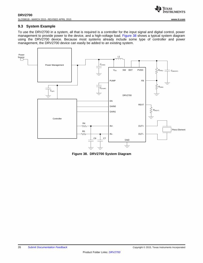
9.3 System ExampleTo use the DRV2700 in a system, all that is required is a controller for the input signal and digital control, powermanagement to provide power to the device, and a high-voltage load. Figure 38 shows a typical system diagramusing the DRV2700 device. Because most systems already include some type of controller and powermanagement, the DRV2700 device can easily be added to an existing system.
Figure 38. DRV2700 System Diagram
26 Submit Documentation Feedback Copyright © 2015, Texas Instruments Incorporated
Product Folder Links: DRV2700

DRV2700www.ti.com SLOS861B –MARCH 2015–REVISED APRIL 2015
10 Power Supply RecommendationsThe recommended voltage supply range for the DRV8662 device is 3 to 5.5 V. For proper operation, place a 0.1-µF low-equivalent series resistance (ESR) supply-bypass capacitor of X5R or X7R type near the VDD pin. Thisbypass capacitor should have a voltage rating of at least 10 V. The internal charge pump requires a 0.1-µFcapacitor of X5R or X7R type with a voltage rating of 10 V or greater to be placed between the PUMP pin andground for proper operation and stability. Do not use the charge pump as a voltage source for any other devices.
11 Layout
11.1 Layout Guidelines
11.1.1 Boost + Amplifier Configuration Layout ConsiderationsTo achieve ideal device performance, use of the thermal footprint outlined by this data sheet is recommended.See the land pattern diagram in the Mechanical, Packaging, and Orderable Information section for exactdimensions. The thermal pad of the DRV2700 device must be soldered directly to the thermal pad on the printedcircuit board (PCB). The thermal pad of the PCB must be connected to the ground net with thermal vias to anyexisting backside or internal copper ground planes. Connection to a ground plane on the top layer near thecorners of the device is also recommended.
Additionally to help minimize crosstalk between the FB voltage and the SW signal, keep the boost programmingresistors (RFB1 and RFB2) as close as possible to the FB pin of the DRV2700 device. Routing this traceunderneath the middle of the inductor is also helpful. If possible, provide a grounding plane between the twosignals.
Lastly, keep the BST trace and plane as large as possible to help minimize the resistance and inductance.
11.1.2 Flyback Configuration Layout ConsiderationsTo achieve ideal device performance, use of the thermal footprint outlined by this data sheet is recommended.See the land pattern diagram in the Mechanical, Packaging, and Orderable Information section for exactdimensions. The thermal pad of the DRV2700 device must be soldered directly to the thermal pad on the PCB.The thermal pad of the PCB must be connected to the ground net with thermal vias to any existing backside orinternal copper ground planes. Connection to a ground plane on the top layer near the corners of the device isalso recommended.
Additionally, minimizing the capacitance on the SW node is very important. Minimizing this capacitance isaccomplished by placing the transformer very close to the SW pin and by removing the ground plane beneaththe transformer pads.
Copyright © 2015, Texas Instruments Incorporated Submit Documentation Feedback 27
Product Folder Links: DRV2700

Large GND plane to provide
good thermal
dissipation
Removed GND plane to minimize capacitance
Transformer
DRV2700
Short trace to minimize capacitance
Inductor
DRV2700
Large GND planeto provide good
thermal dissipation
Both feedbackresistors are placed
near the FB pin tominimize coupling
from the SW pin Large BST planeto minimize traceresistance andinductance
DRV2700SLOS861B –MARCH 2015–REVISED APRIL 2015 www.ti.com
11.2 Layout Example
Figure 39. DRV2700 Boost + Amplifier Layout Example
Figure 40. DRV2700 Flyback Layout Example
28 Submit Documentation Feedback Copyright © 2015, Texas Instruments Incorporated
Product Folder Links: DRV2700
DRV2700www.ti.com SLOS861B –MARCH 2015–REVISED APRIL 2015
12 Device and Documentation Support
12.1 Documentation Support
12.1.1 Related DocumentationFor related documentation see the following:
DRV2700EVM High Voltage Piezo Driver Evaluation Kit, SLOU403
12.2 TrademarksAll trademarks are the property of their respective owners.
12.3 Electrostatic Discharge CautionThese devices have limited built-in ESD protection. The leads should be shorted together or the device placed in conductive foamduring storage or handling to prevent electrostatic damage to the MOS gates.
12.4 GlossarySLYZ022 — TI Glossary.
This glossary lists and explains terms, acronyms, and definitions.
13 Mechanical, Packaging, and Orderable InformationThe following pages include mechanical, packaging, and orderable information. This information is the mostcurrent data available for the designated devices. This data is subject to change without notice and revision ofthis document. For browser-based versions of this data sheet, refer to the left-hand navigation.
Copyright © 2015, Texas Instruments Incorporated Submit Documentation Feedback 29
Product Folder Links: DRV2700

PACKAGE OPTION ADDENDUM
www.ti.com 31-Mar-2018
Addendum-Page 1
PACKAGING INFORMATION
Orderable Device Status(1)
Package Type PackageDrawing
Pins PackageQty
Eco Plan(2)
Lead/Ball Finish(6)
MSL Peak Temp(3)
Op Temp (°C) Device Marking(4/5)
Samples
DRV2700RGPR ACTIVE QFN RGP 20 3000 Green (RoHS& no Sb/Br)
CU NIPDAU Level-2-260C-1 YEAR -40 to 85 DRV2700
DRV2700RGPT ACTIVE QFN RGP 20 250 Green (RoHS& no Sb/Br)
CU NIPDAU Level-2-260C-1 YEAR -40 to 85 DRV2700
(1) The marketing status values are defined as follows:ACTIVE: Product device recommended for new designs.LIFEBUY: TI has announced that the device will be discontinued, and a lifetime-buy period is in effect.NRND: Not recommended for new designs. Device is in production to support existing customers, but TI does not recommend using this part in a new design.PREVIEW: Device has been announced but is not in production. Samples may or may not be available.OBSOLETE: TI has discontinued the production of the device.
(2) RoHS: TI defines "RoHS" to mean semiconductor products that are compliant with the current EU RoHS requirements for all 10 RoHS substances, including the requirement that RoHS substancedo not exceed 0.1% by weight in homogeneous materials. Where designed to be soldered at high temperatures, "RoHS" products are suitable for use in specified lead-free processes. TI mayreference these types of products as "Pb-Free".RoHS Exempt: TI defines "RoHS Exempt" to mean products that contain lead but are compliant with EU RoHS pursuant to a specific EU RoHS exemption.Green: TI defines "Green" to mean the content of Chlorine (Cl) and Bromine (Br) based flame retardants meet JS709B low halogen requirements of <=1000ppm threshold. Antimony trioxide basedflame retardants must also meet the <=1000ppm threshold requirement.
(3) MSL, Peak Temp. - The Moisture Sensitivity Level rating according to the JEDEC industry standard classifications, and peak solder temperature.
(4) There may be additional marking, which relates to the logo, the lot trace code information, or the environmental category on the device.
(5) Multiple Device Markings will be inside parentheses. Only one Device Marking contained in parentheses and separated by a "~" will appear on a device. If a line is indented then it is a continuationof the previous line and the two combined represent the entire Device Marking for that device.
(6) Lead/Ball Finish - Orderable Devices may have multiple material finish options. Finish options are separated by a vertical ruled line. Lead/Ball Finish values may wrap to two lines if the finishvalue exceeds the maximum column width.
Important Information and Disclaimer:The information provided on this page represents TI's knowledge and belief as of the date that it is provided. TI bases its knowledge and belief on informationprovided by third parties, and makes no representation or warranty as to the accuracy of such information. Efforts are underway to better integrate information from third parties. TI has taken andcontinues to take reasonable steps to provide representative and accurate information but may not have conducted destructive testing or chemical analysis on incoming materials and chemicals.TI and TI suppliers consider certain information to be proprietary, and thus CAS numbers and other limited information may not be available for release.
In no event shall TI's liability arising out of such information exceed the total purchase price of the TI part(s) at issue in this document sold by TI to Customer on an annual basis.
PACKAGE OPTION ADDENDUM
www.ti.com 31-Mar-2018
Addendum-Page 2

TAPE AND REEL INFORMATION
*All dimensions are nominal
Device PackageType
PackageDrawing
Pins SPQ ReelDiameter
(mm)
ReelWidth
W1 (mm)
A0(mm)
B0(mm)
K0(mm)
P1(mm)
W(mm)
Pin1Quadrant
DRV2700RGPR QFN RGP 20 3000 330.0 12.4 4.25 4.25 1.15 8.0 12.0 Q2
DRV2700RGPT QFN RGP 20 250 180.0 12.4 4.25 4.25 1.15 8.0 12.0 Q2
PACKAGE MATERIALS INFORMATION
www.ti.com 27-Apr-2015
Pack Materials-Page 1

*All dimensions are nominal
Device Package Type Package Drawing Pins SPQ Length (mm) Width (mm) Height (mm)
DRV2700RGPR QFN RGP 20 3000 367.0 367.0 35.0
DRV2700RGPT QFN RGP 20 250 210.0 185.0 35.0
PACKAGE MATERIALS INFORMATION
www.ti.com 27-Apr-2015
Pack Materials-Page 2


IMPORTANT NOTICE
Texas Instruments Incorporated (TI) reserves the right to make corrections, enhancements, improvements and other changes to itssemiconductor products and services per JESD46, latest issue, and to discontinue any product or service per JESD48, latest issue. Buyersshould obtain the latest relevant information before placing orders and should verify that such information is current and complete.TI’s published terms of sale for semiconductor products (http://www.ti.com/sc/docs/stdterms.htm) apply to the sale of packaged integratedcircuit products that TI has qualified and released to market. Additional terms may apply to the use or sale of other types of TI products andservices.Reproduction of significant portions of TI information in TI data sheets is permissible only if reproduction is without alteration and isaccompanied by all associated warranties, conditions, limitations, and notices. TI is not responsible or liable for such reproduceddocumentation. Information of third parties may be subject to additional restrictions. Resale of TI products or services with statementsdifferent from or beyond the parameters stated by TI for that product or service voids all express and any implied warranties for theassociated TI product or service and is an unfair and deceptive business practice. TI is not responsible or liable for any such statements.Buyers and others who are developing systems that incorporate TI products (collectively, “Designers”) understand and agree that Designersremain responsible for using their independent analysis, evaluation and judgment in designing their applications and that Designers havefull and exclusive responsibility to assure the safety of Designers' applications and compliance of their applications (and of all TI productsused in or for Designers’ applications) with all applicable regulations, laws and other applicable requirements. Designer represents that, withrespect to their applications, Designer has all the necessary expertise to create and implement safeguards that (1) anticipate dangerousconsequences of failures, (2) monitor failures and their consequences, and (3) lessen the likelihood of failures that might cause harm andtake appropriate actions. Designer agrees that prior to using or distributing any applications that include TI products, Designer willthoroughly test such applications and the functionality of such TI products as used in such applications.TI’s provision of technical, application or other design advice, quality characterization, reliability data or other services or information,including, but not limited to, reference designs and materials relating to evaluation modules, (collectively, “TI Resources”) are intended toassist designers who are developing applications that incorporate TI products; by downloading, accessing or using TI Resources in anyway, Designer (individually or, if Designer is acting on behalf of a company, Designer’s company) agrees to use any particular TI Resourcesolely for this purpose and subject to the terms of this Notice.TI’s provision of TI Resources does not expand or otherwise alter TI’s applicable published warranties or warranty disclaimers for TIproducts, and no additional obligations or liabilities arise from TI providing such TI Resources. TI reserves the right to make corrections,enhancements, improvements and other changes to its TI Resources. TI has not conducted any testing other than that specificallydescribed in the published documentation for a particular TI Resource.Designer is authorized to use, copy and modify any individual TI Resource only in connection with the development of applications thatinclude the TI product(s) identified in such TI Resource. NO OTHER LICENSE, EXPRESS OR IMPLIED, BY ESTOPPEL OR OTHERWISETO ANY OTHER TI INTELLECTUAL PROPERTY RIGHT, AND NO LICENSE TO ANY TECHNOLOGY OR INTELLECTUAL PROPERTYRIGHT OF TI OR ANY THIRD PARTY IS GRANTED HEREIN, including but not limited to any patent right, copyright, mask work right, orother intellectual property right relating to any combination, machine, or process in which TI products or services are used. Informationregarding or referencing third-party products or services does not constitute a license to use such products or services, or a warranty orendorsement thereof. Use of TI Resources may require a license from a third party under the patents or other intellectual property of thethird party, or a license from TI under the patents or other intellectual property of TI.TI RESOURCES ARE PROVIDED “AS IS” AND WITH ALL FAULTS. TI DISCLAIMS ALL OTHER WARRANTIES ORREPRESENTATIONS, EXPRESS OR IMPLIED, REGARDING RESOURCES OR USE THEREOF, INCLUDING BUT NOT LIMITED TOACCURACY OR COMPLETENESS, TITLE, ANY EPIDEMIC FAILURE WARRANTY AND ANY IMPLIED WARRANTIES OFMERCHANTABILITY, FITNESS FOR A PARTICULAR PURPOSE, AND NON-INFRINGEMENT OF ANY THIRD PARTY INTELLECTUALPROPERTY RIGHTS. TI SHALL NOT BE LIABLE FOR AND SHALL NOT DEFEND OR INDEMNIFY DESIGNER AGAINST ANY CLAIM,INCLUDING BUT NOT LIMITED TO ANY INFRINGEMENT CLAIM THAT RELATES TO OR IS BASED ON ANY COMBINATION OFPRODUCTS EVEN IF DESCRIBED IN TI RESOURCES OR OTHERWISE. IN NO EVENT SHALL TI BE LIABLE FOR ANY ACTUAL,DIRECT, SPECIAL, COLLATERAL, INDIRECT, PUNITIVE, INCIDENTAL, CONSEQUENTIAL OR EXEMPLARY DAMAGES INCONNECTION WITH OR ARISING OUT OF TI RESOURCES OR USE THEREOF, AND REGARDLESS OF WHETHER TI HAS BEENADVISED OF THE POSSIBILITY OF SUCH DAMAGES.Unless TI has explicitly designated an individual product as meeting the requirements of a particular industry standard (e.g., ISO/TS 16949and ISO 26262), TI is not responsible for any failure to meet such industry standard requirements.Where TI specifically promotes products as facilitating functional safety or as compliant with industry functional safety standards, suchproducts are intended to help enable customers to design and create their own applications that meet applicable functional safety standardsand requirements. Using products in an application does not by itself establish any safety features in the application. Designers mustensure compliance with safety-related requirements and standards applicable to their applications. Designer may not use any TI products inlife-critical medical equipment unless authorized officers of the parties have executed a special contract specifically governing such use.Life-critical medical equipment is medical equipment where failure of such equipment would cause serious bodily injury or death (e.g., lifesupport, pacemakers, defibrillators, heart pumps, neurostimulators, and implantables). Such equipment includes, without limitation, allmedical devices identified by the U.S. Food and Drug Administration as Class III devices and equivalent classifications outside the U.S.TI may expressly designate certain products as completing a particular qualification (e.g., Q100, Military Grade, or Enhanced Product).Designers agree that it has the necessary expertise to select the product with the appropriate qualification designation for their applicationsand that proper product selection is at Designers’ own risk. Designers are solely responsible for compliance with all legal and regulatoryrequirements in connection with such selection.Designer will fully indemnify TI and its representatives against any damages, costs, losses, and/or liabilities arising out of Designer’s non-compliance with the terms and provisions of this Notice.
Mailing Address: Texas Instruments, Post Office Box 655303, Dallas, Texas 75265Copyright © 2018, Texas Instruments Incorporated