drv-fingerprinting: using data retention voltage of sram - spqr
TRANSCRIPT

DRV-Fingerprinting: Using Data RetentionVoltage of SRAM Cells for Chip Identification∗
Daniel E. HolcombUC Berkeley
Amir RahmatiUMass Amherst
Mastooreh SalajeghehUMass Amherst
Wayne P. BurlesonUMass Amherst
Kevin FuUMass Amherst
Abstract
Physical unclonable functions (PUFs) produce outputs that are afunction of minute random physical variations. Promoted for low-costauthentication and resistance to counterfeiting, many varieties of PUFshave been used to enhance the security and privacy of RFID tags. Todifferent extents, applications for both identification and authenticationrequire a PUF to produce a consistent output over time. As the sensing ofminute variations is a fundamentally noisy process, much effort is spent onerror correction of PUF outputs. We propose a new variant of PUF thatuses well-understood properties of common memory cells as a fingerprint.Our method of fingerprinting SRAM cells by their data retention voltageimproves the success rate of identification by 28% over fingerprints basedon power-up state.
1 Introduction
RFID circuits can be identified or authenticated using static identifiers stored innon-volatile memory or through the use of identifying physical characteristics.Physical characteristics have several security advantages over static identifiers,including immutability and resistance to cloning and tampering. The physicalcharacteristics can be viewed as an identifying fingerprint of a given device. Moreformally, physical fingerprints are a component of a particular type of physicalunclonable function (PUF) that is originally described as a physically obfuscatedkey [4], and more recently as a weak PUF [6].
If used for identification or constructing secret keys, fingerprint observationsmust be consistent over time. Sensing the microscopic variations that makeeach device unique while also minimizing the impact of noise is a fundamental
∗Accepted to appear at the 8th Workshop on RFID Security and Privacy, July 2012

concern in PUFs. Much effort is spent on error correction of somewhat-unreliablefingerprints or PUF outputs. Error correcting codes are expensive in terms ofthe number of raw bits required to create a reliable key, and more so if thenumber of correctable errors must be large. Toward this goal, we present anew fingerprinting method that is more reliable across trials than comparableprevious approaches.
In this work we propose a new method for chip fingerprinting that uses DataRetention Voltage (DRV) in SRAM as the identifier. The DRV of an SRAM isthe minimum voltage at which its cells can retain state. DRV fingerprints arefound to be more informative than other approaches for fingerprinting SRAMthat have been proposed in research [6, 8] and commercially.1 The physicalcharacteristics responsible for DRV are imparted randomly during manufacturingand therefore serve as a natural barrier against counterfeiting. The proposedtechnique has the potential for wide application, as SRAM cells are among themost common building blocks of nearly all digital systems including smart cardsand programmable RFID tags.
The contributions of this work are as follows:
• Demonstrating that the DRVs of SRAM cells are consistent fingerprintscapable of identifying devices among a population.
• Demonstrating that DRV fingerprints make use of physical variations in a waythat is similar to SRAM power-up fingerprints, but that DRV fingerprintshave the potential for more accurate identification.
The remainder of this paper is structured as follows: Section 2 introducesdata retention voltage. Section 3 explains how the DRVs of SRAM cells arecharacterized. Section 4 evaluates DRV fingerprinting using experimental data.Sections 5 and 6 review related work and present directions for future work.
2 Data Retention Voltage
A data retention failure is said to occur when an SRAM cell spuriously flipsstate due to insufficient supply voltage. The data retention voltage (DRV) of anSRAM array signifies the minimum supply voltage at which all SRAM cells canstore arbitrary state. DRV is studied in the literature as a limit to supply voltagescaling. Various simulation models [25, 2, 12] and silicon measurements [15] showmodern SRAM DRVs to be under 300mV. Most previous literature focuses oncases where the supply voltage of the circuit remains safely above DRV. Whileremaining above DRV, the supply voltage can be adjusted to reduce leakagepower [3], compensate for manufacturing variability [12], or compensate forenvironmental variations [25].
Each SRAM cell uses the positive feedback of cross-coupled inverters tohold state on two complementary storage nodes. Retention failures occur atlow supply voltages because the low voltage weakens the positive feedback ofthe cross-coupled inverters. Due to asymmetric process variation, at some low
1http://www.intrinsic-id.com/
2

20100
200300
20100
200300
0
0.05
0.1
0.15
v1
c [mV]v0
c [mV]
Freq
uenc
y
Figure 1: The joint probability distribution function over all cells of the twovariables (v0c and v1c ) comprising a DRV characterization. The distribution isdetermined experimentally using Algorithm 1, and shows that a large fraction ofcells have the minimum possible value of 20mV for either v0 or v1, but none havethe minimum value (or near-minimum values) for both. A cell with a minimumvalue for v0 or v1 is a cell that retains one written state across all test voltages.
supply voltages a transition from a written state to the opposite state becomesinevitable; observations about the direction of such transitions and the voltagesat which they occur are the basis for DRV fingerprints. Any collection of SRAMcells has a distinctive DRV fingerprint because of its unique random processvariation.
3 Characterizing the DRV of an SRAM Cell
The DRVs of SRAM cells are characterized by repeatedly lowering the SRAMsupply voltage and observing the highest voltage at which each cell fails. Ifthe SRAM supply node also supplies the processing core, then the low voltagesused for the characterization will cause the core to reset and lose its state.Our experiments avoid this difficulty by using non-volatile memory to maintainpersistency across the low voltages. However, a custom integrated circuit designedfor DRV fingerprinting can also avoid this difficulty by using an SRAM supplynode that is decoupled from the nominal supply node of the processor. This isoften done, for example, in power-gated circuits where unused on-chip functionalblocks are turned off entirely while the chip as a whole remains powered.
We characterize the DRV of an SRAM cell c with a pair 〈v0c , v1c 〉. Each vwcin the pair represents the highest voltage at which cell c will have a retentionfailure after state w is written to it. In principle, v0c and v1c are real-valued; butin practice, we approximate each using one of N = (300mV − 20mV )/∆ discretevalues as shown in Algorithm 1. With ∆ set at 10mV, the N = 28 possiblevalues for v0c and v1c are {20mV, 30mV, . . . , 290mV }. The frequency of observingdifferent DRV pairs is shown in the joint probability distribution function ofvariables v0c and v1c in Fig. 1.
3

Algorithm 1 Characterize the DRV fingerprint of a set of SRAM cells.
Prerequisite: C – a set of SRAM cellsEnsure: v0c , v
1c – the DRV characterizations of each SRAM cell c ∈ C.
1: Let Vnom be the nominal supply voltage (Vdd) for the chip2: Let sc refer to the logical state of SRAM cell c ∈ C.3: Let s′c refer to the logical state of NVM cell that corresponds to SRAM cell c.
4: for w = 0, 1 do5: for c ∈ C do6: sc ← w {write w into SRAM cell}7: s′c ← w {write w into NVM cell}8: vwc ← 0 {value used if no retention failure observed}9: end for
10: vtest ← 300mV {initialize test voltage}11: while vtest > 20mV do12: lower chip voltage from Vnom to vtest13: wait for twait seconds14: raise chip voltage from vtest to Vnom
15: for c ∈ C do16: if (sc = ¬w) ∧ (s′c = w) then17: SRAM cell c had a retention failure from state w at voltage vtest, but
previously had no failure at voltage vtest+∆. Therefore vtest approximatesthe largest voltage that induces a retention failure after writing w.
18: vwc ← vtest19: end if20: s′c ← sc {write SRAM to NVM}21: end for22: vtest ← vtest −∆ {try a lower voltage next}23: end while
24: end for
3.1 Experimental Setup
We examine the DRV of SRAM cells using Algorithm 1 implemented as follows:A microcontroller runs a program that sets all available memory bits to either 1or 0. The supply voltage is then decreased to a value between 300mV and 20mV(∆ = 10mV ) for 5 seconds. When supply voltage is restored to 3V, the programstores the content of SRAM to the flash memory. Note that we conservatively usetwait = 5s to avoid missing marginal failures. Simulations by Nourivand et al. [12]using a procedure similar to Algorithm 1 show that waiting for twait = 2ms ata reduced supply voltage is sufficient to observe retention failures. An AgilentU2541A-series data acquisition (DAQ) unit controls the supply voltage and thetiming of when voltage is raised and lowered. Thermal tests are conductedinside of a Sun Electronics EC12 Environmental Chamber [22], and an OSXL450infrared non-contact thermometer [13] with ±2◦C accuracy is used to verify thetemperature. All experiments use instances of Texas Instruments MSP430 F2131microcontrollers with 256 bytes of SRAM, of which 240 bytes are available forDRV fingerprinting. The DRV of each cell is characterized 20 times. The total
4

OutcomeFreq.〈v0c , v1c 〉
〈130mV , 100mV 〉 0.0096
〈120mV , 100mV 〉 0.0076
〈130mV , 110mV 〉 0.0070
〈120mV , 110mV 〉 0.0070
(a) Most common weak DRVs
OutcomeFreq.〈v0c , v1c 〉
〈20mV , 130mV 〉 0.0893
〈20mV , 120mV 〉 0.0719
〈130mV , 20mV 〉 0.0685
〈20mV , 140mV 〉 0.0651
(b) Most common strong DRVs
Table 1: The 4 most commonly observed weak and strong DRV characterizations,and the probability of observing each in a randomly selected trial.
runtime to characterize all 240 bytes of SRAM on a chip once using Algorithm 1 isgiven by tproc in Eq. 1, and is 140 seconds for the conservative case of ∆ = 10mVand twait = 5s.
tproc = twait ×300mV − 20mV
∆(1)
3.2 Information Content of SRAM Cell DRV
The DRV of each cell has N2 possible outcomes representing all combinations ofN outcomes for v0c and the N outcomes for v1c (in our case N = 28). The DRVof each cell is then a random variable X with N2 outcomes denoted x0 throughxN2−1. The total entropy H(X) is the expected information value of the DRV ofan unknown cell. Entropy depends (per Eq. 2) on the probabilities of each DRVoutcome, denoted p(xi). In the ideal case where all N2 outcomes are equallylikely (e.g. p(xi) = 1/N2 for all xi), each DRV would have almost 10 bits ofentropy. Applying Eq. 2 to the decidedly non-uniform outcome probabilities ofFig. 1 shows the actual entropy of a DRV to be 5.12 bits. The most frequentlyobserved DRV outcomes are given in Table. 1.
Eq. 1 shows that runtime is inversely proportional to ∆, so we consider theinformation loss from making ∆ larger than 10mV. Fig. 2 shows the ideal andactual entropy of DRV characterizations when different values of ∆ are used. Inthe extreme case where ∆ = 140mV , variables v0c and v1c are each restricted tothe values {20mV, 160mV }, so the ideal entropy of the DRV is equivalent to 2flips of a fair coin. The values of ∆ used in Fig. 2 are chosen on account of beingunambiguously recreatable from the ∆ = 10mV data.
H(X) = −∑i=1
p(xi) log p(xi) (2)
5

0 10 20 40 70 1400
2
4
6
8
10
∆ [mV]
Ent
ropy
[bi
ts p
er c
ell]
idealactual
Figure 2: Sweeping ∆ from 10mV to 140mV shows that a loss of measurementprecision reduces entropy of each cell’s DRV characterization.
3.3 Observations about Strong and Weak Cells
We abstract the N2 possible DRV characterizations (Fig. 1) into three classes2
that are sufficient to demonstrate general observations about all DRVs:
• A strongly 0 DRV characterization is a pair 〈v0c , v1c 〉 such that v0c = 20mVand v1c > 20mV . A strongly 0 DRV indicates that no retention failureoccurs at any voltage vtest after state 0 is written.
• A strongly 1 DRV characterization is a pair 〈v0c , v1c 〉 such that v0c > 20mVand v1c = 20mV . A strongly 1 DRV indicates that no retention failureoccurs at any voltage vtest after state 1 is written.
• A weak DRV characterization is a pair 〈v0c , v1c 〉 such that v0c > 20mV andv1c > 20mV . A weak DRV indicates that a failure is observed at somevoltage vtest after each state is written.
The variation-dependent behavior of an SRAM cell occurs somewhere between20mV and 300mV for each cell; above 300mV all cells can reliably hold eitherthe 0 or the 1 state, and below 20mV no cells can do so. When a cell produces astrongly 0 or strongly 1 characterization, it means (per Algorithm 1) that forone written state the supply voltage is lowered all the way through the sensitiveregion down to 20mV and then raised back up without causing a failure. Astrongly 0 or strongly 1 characterization therefore indicates a strong preferencefor one state over the other at all supply voltages. A weak characterization iswhen each written state flips at some voltage within the sensitive region, andneither state can be retained down to 20mV.
Both strong and weak DRV characterizations are largely repeatable acrosstrials. Fig. 3 shows the distribution of DRVs produced by randomly selected cellsfor which the first DRV produced is one of the 4 most commonly observed weakDRVs from Table 1a; each plot shows the conditional probability distribution of
2Note that no observation of 〈v0c , v1v〉 = 〈20mV, 20mV 〉 is ever made, so we do not includethis outcome in any of the three cases.
6

a subsequent DRV characterization. Occasionally the same cells that producea weak DRV produce a strong DRV in subsequent trials. Fig. 4 shows thesame analysis for the 4 most commonly observed strong DRVs; none of the cellssubsequently produces the opposite strong characterization.
100 200
100
200
v0
c [mV]
target = 130mV,100mV
v1 c [m
V]
0.1
0.2
0.3
0.4
100 200
100
200
v0
c [mV]
target = 120mV,100mV
v1 c [m
V]
0.02
0.04
0.06
0.08
0.1
0.12
100 200
100
200
v0
c [mV]
target = 130mV,110mV
v1 c [m
V]
0
0.1
0.2
0.3
0.4
100 200
100
200
v0
c [mV]
target = 120mV,110mV
v1 c [m
V]
0
0.05
0.1
0.15
Figure 3: For each of the 4 most frequently observed weak DRVs (see Table 1a),the DRV in a second trial from a cell that produced the frequently observedDRV in a first trial.
3.4 Relation to Power-up State
It is known that SRAM cells consistently power-up to the same state [6, 8] ina majority of trials. Cells with highly reliable power-up states tend to be thesame cells with strong DRV characterizations. Fig. 5 shows the mean power-upstate over 28 trials for cells that produced a strongly 0 or strongly 1 DRVcharacterization. Among cells with strongly 0 DRV, 98.6% power-up to the 0state in all 28 power-up trials (Fig. 5a). Similarly, 95.1% of cells characterizedas strongly 1 consistently power-up to the 1 state (Fig. 5a). Although a strongDRV fingerprint is correlated to power-up tendency, the DRV provides a moreinformative identifier than does power-up by providing information about themaximum voltage at which the unfavored state cannot be reliably stored.
7

100 200
100
200
v0
c [mV]
target = 20mV,130mV
v1 c [m
V]
0
0.1
0.2
0.3
0.4
0.5
100 200
100
200
v0
c [mV]
target = 20mV,120mV
v1 c [m
V]
0
0.1
0.2
0.3
0.4
100 200
100
200
v0
c [mV]
target = 130mV,20mV
v1 c [m
V]
0
0.1
0.2
0.3
100 200
100
200
v0
c [mV]
target = 20mV,140mV
v1 c [m
V]
0
0.2
0.4
0.6
Figure 4: For each of the 4 most frequently observed strong DRVs (see Table. 1b),the DRV in a second trial from a cell that produced the frequently observedDRV in a first trial.
4 Fingerprint Matching
A DRV fingerprint is obtained from a single characterization of a set of adjacentcells within an SRAM. A k-bit fingerprint Fi comprises cell characterizations〈v0i , v1i 〉, 〈v0i+1, v
1i+1〉, . . . , 〈v0i+k−1, v
1i+k−1〉. The difference between fingerprints is
the sum of the differences between their corresponding single-cell characteriza-tions. Recalling that each DRV is a point 〈v0c , v1c 〉 in 2-dimensional space, wedefine the distance between two DRVs according to the square of their distancealong each dimension (Eq. 3). For comparison, a second metric used is theHamming distance between power-up trials; this is shown by Eq. 4, where pi isthe state of the ith bit of SRAM after a power-up.
d1(Fi, Fj) =
k−1∑n=0
(v0i+n − v0j+n
)2+(v1i+n − v1j+n
)2(3)
hd(Fi, Fj) =
k−1∑n=0
pi+n ⊕ pj+n (4)
8

0 0.5 10
0.5
1 Pr(x=0)=0.986
Mean Power−up StateF
requ
ency
(a) Strongly 0 DRV
0 0.5 10
0.5
1 Pr(x=1)=0.951
Mean Power−up State
Fre
quen
cy
(b) Strongly 1 DRV
Figure 5: The plot at left shows that 98.6% of SRAM cells that produce astrongly 0 DRV reliably power-up to state 0, as observed by a mean power-upstate of 0. The plot at right shows that 95.1% of cells with strongly 1 DRVsreliably power-up to state 1. The DRV is from a single trial of the cell, and themean power-up state is measured over 28 power-up trials.
Strongly 0 Weak Strongly 1
Strongly 0 35.80% 3.10% 0.00%
Weak - 24.98% 2.48%
Strongly 1 - - 33.64%
Table 2: Probability of different pairwise outcomes when 2 DRV fingerprints aretaken from a randomly chosen cell. Over the 5000 samples collected, no cell everhas a DRV that is strongly 1 in one trial and strongly 0 in another, but 5.6% ofoutcomes have one strong and one weak DRV.
4.1 Identification at Nominal Temperature
At the nominal operating temperature of 29◦C, three experiments compare DRVfingerprints with power-up fingerprints. These experiments are explained inthe following subsections; the first shows the histograms of distances betweenfingerprints, and the second and third evaluate the accuracy of distance-basedmatching.
4.1.1 Histogram of Distances Between Fingerprints
A first experiment shows that DRV fingerprints are repeatable and unique, as isnecessary for successfully identifying chips within a population. Within-classpairings are of multiple fingerprints generated by the same set of cells on the samedevice. Between-class pairings are from different sets of cells on the same device,or from any sets of cells on different devices. The similarity of any two fingerprintsis quantified by a distance, and this distance is the basis for determining thecorrect identity of a fingerprint. If within-class fingerprint pairings consistentlyhave smaller distances than between-class pairings, then it is possible to determineidentity by choosing an appropriate threshold that separates the two classes. Thehistograms of within-class and between-class distances for DRV and power-upfingerprints are shown in Fig. 6. These histograms represent all data collectedfrom the MSP430F2131 microcontrollers at room temperature. The distances
9
on the x-axes are not directly comparable across metrics; of importance is onlywhether the two classes are clearly separable within each plot.
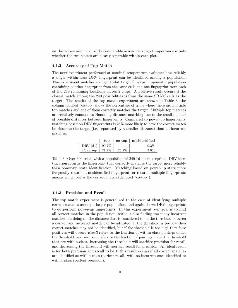
4.1.2 Accuracy of Top Match
The next experiment performed at nominal temperature evaluates how reliablya single within-class DRV fingerprint can be identified among a population.This experiment matches a single 16-bit target fingerprint against a populationcontaining another fingerprint from the same cells and one fingerprint from eachof the 239 remaining locations across 2 chips. A positive result occurs if theclosest match among the 240 possibilities is from the same SRAM cells as thetarget. The results of the top match experiment are shown in Table 3; thecolumn labelled “co-top” shows the percentage of trials where there are multipletop matches and one of them correctly matches the target. Multiple top matchesare relatively common in Hamming distance matching due to the small numberof possible distances between fingerprints. Compared to power-up fingerprints,matching based on DRV fingerprints is 28% more likely to have the correct matchbe closer to the target (i.e. separated by a smaller distance) than all incorrectmatches.
top co-top misidentified
DRV (d1) 99.7% - 0.3%
Power-up 71.7% 24.7% 3.6%
Table 3: Over 300 trials with a population of 240 16-bit fingerprints, DRV iden-tification returns the fingerprint that correctly matches the target more reliablythan power-up state identification. Matching based on power-up state morefrequently returns a misidentified fingerprint, or returns multiple fingerprintsamong which one is the correct match (denoted “co-top”).
4.1.3 Precision and Recall
The top match experiment is generalized to the case of identifying multiplecorrect matches among a larger population, and again shows DRV fingerprintsto outperform power-up fingerprints. In this experiment, our goal is to findall correct matches in the population, without also finding too many incorrectmatches. In doing so, the distance that is considered to be the threshold betweena correct and incorrect match can be adjusted. If the threshold is too low thencorrect matches may not be identified, but if the threshold is too high then falsepositives will occur. Recall refers to the fraction of within-class pairings underthe threshold, and precision refers to the fraction of pairings under the thresholdthat are within-class. Increasing the threshold will sacrifice precision for recall,and decreasing the threshold will sacrifice recall for precision. An ideal resultis for both precision and recall to be 1; this result occurs if all correct matchesare identified as within-class (perfect recall) with no incorrect ones identified aswithin-class (perfect precision).
10

0 0.1 0.2 0.3 0.4 0.5 0.60
0.5
1
d1(Fi, F
j)
Freq
uenc
y
within classbetween class
0 5 10 150
0.5
1
hd( Fi , F
j )
Freq
uenc
y
within classbetween class
Figure 6: Within-class and between-class distances of 16-bit fingerprints. Theupper plot uses DRV fingerprints with distance metric d1 from Eq. 3. The lowerplot uses power-up fingerprints with Hamming distance as a metric.
The precision and recall plots of Fig. 7 are obtained by iterating the followingprocedure. One 16-bit segment of SRAM is chosen for identification. Onefingerprint trial from this segment is chosen at random as the target, and itis matched against a population of 1019 fingerprints comprising 19 from thesame SRAM segment (within-class pairings) and 1000 non-matching fingerprints(between-class pairings). The non-matching fingerprints are randomly selectedamong 20 trials from 239 other segments of SRAM3. The matching threshold isswept to find achievable precision-versus-recall tradeoffs, and each achievabletradeoff is a point in Fig. 7. The large number of tradeoff points in the plot iscollected from multiple iterations of this procedure. The general trend is thatDRV fingerprints produce better recall for a given precision, or better precisionfor a given recall compared to power-up fingerprints.
0 0.25 0.5 0.75 10
0.25
0.5
0.75
1
Recall
Prec
isio
n
DRV (d1)
0 0.25 0.5 0.75 10
0.25
0.5
0.75
1
Recall
Pre
cisi
on
Power−up
Figure 7: Tradeoff points of precision and recall for trials of DRV fingerprintsare generally closer to the ideal result of perfect precision and recall.
3The 239 eligible 16-bit segments are the 119 remaining on the target’s own chip, and all120 such locations on the other device.
11

4.2 Impact of Temperature Variations
Given that DRV fingerprints would likely be used in real-world scenarios withoutprecisely-controlled temperatures, a final experiment explores the impact oftemperature on DRV fingerprints. This experiment is similar to the experimentof subsection 4.1.1, but the pairs of fingerprint observations used to generatethe within-class distances are now made at different temperatures. The resultsare shown in Fig. 8. The increase of within-class distances across temperatureimplies a diminished reliability. To compensate for this, larger fingerprints(comprising more bits) may be needed for identification, and more robust errorcorrecting codes may be needed in key-generation applications. If the increasedwithin-class distances are due to a uniform shift in the DRVs of all cells, then apromising direction for future work would be to design a matching scheme thatis insensitive to this type of uniform shift.
0 0.1 0.2 0.30
0.5
1
d1(Fi,F
j)
Freq
uenc
y
within class: 27° C vs 27° C
within class: 27° C vs 32° Cwithin class: 27° C vs 40° C
between class: 27° C vs 27° C
Figure 8: The line plots show within-class distances when one fingerprint ob-servation is made at 27◦C and the second at 27◦C, 32◦C, or 40◦C; within-classdistances increase with temperature, implying a diminished reliability. The barplot shows between-class distances of 16-bit fingerprints taken at 27◦C. Becausethere does not exist a distance threshold that can separate the two classes whentemperature is varied, it may be necessary to use larger fingerprints for reliableidentification.
5 Related Works
A wide variety of PUFs and fingerprints based on custom or pre-existing inte-grated circuit components have been developed. The identifying features used bycustom designs include MOSFET drain-current [10], timing race conditions [5],and the digital state taken by cross-coupled logic after a reset [20]. IC identifi-cation based on pre-existing circuitry is demonstrated using SRAM power-upstate [8, 6], and physical variations of flash memory [14]. Lee et al. [9] derivea secret key unique to each IC using the statistical delay variations of wiresand transistors across ICs. Bhargava et al. explore circuit-level techniques forincreasing the reliability of SRAM PUFs [1]. An experimental evaluation oflow-temperature data remanence on a variety of SRAMs is provided by Sko-robogatov [19], and SRAM remanence in RFID has been studied by Saxena andVoris as a limitation to SRAM-based true random number generation [18].
12

Previous works [23, 17] have used error correction to construct secret keysfrom noisy PUF sources; however, this is expensive in terms of gates and otherresources. To give an idea of the cost of error correction, BCH codes previouslyused with PUFs include one to correct 21 errors among 127 raw bits in creatinga 64-bit key [21], and to correct 102 errors among 1023 raw bits in creating a278-bit key [6]. The work of Guajardo et al. [6] uses a derivative of power-upSRAM state as a secret key; however, it requires an error correction code andimposes SRAM space overhead. Maes et al. [11] introduce an SRAM helper dataalgorithm to mask unreliable bits using low-overhead post-processing algorithms.Recently, Yu et al. [26] proposed a method of error correction for PUFs using anew syndrome coding scheme to minimize the information leaked by the errorcorrection codes, and Hiller et al. extend this approach for SRAM PUFs [7].Van Herrewege et al. [24] have designed a new lightweight authentication schemeusing PUFs that does not require the reader to store a large number of PUFchallenge and response pairs.
Given the low cost of the several bytes of SRAM that are used for DRVfingerprinting, a relatively significant practical cost may be associated with thegeneration of the test voltages for characterizing the DRVs. Emerging devicessuch as computational RFIDs [16] can use software routines to extract DRVs,but as contactless devices they must generate all test voltages on-chip. On-chipdynamic control of SRAM supply voltage is assumed in the low-power literatureat least since work on drowsy caches [3]. Supply voltage tuning has also beenapplied with canary cells to detect potential SRAM failures, and as a post-silicon technique to compensate for process variation and increase manufacturingyields [12].
6 Conclusions and Future Works
This work has demonstrated that SRAM DRV fingerprints are static identifiers ofa device, and it has presented a simple characterization procedure and matchingalgorithms to use them as such. DRV fingerprints are similar to previouslydemonstrated power-up fingerprints, but they provide a more informative non-binary identifier of each cell. As a result of this, DRV fingerprints are identifiedup to 28% more reliably than are power-up fingerprints.
The practical limits of DRV fingerprint performance and reliability shouldbe explored further. Within the constraints of acceptable precision, the runtimeof the characterization procedure can be reduced by increasing the voltagestep size ∆ and reducing the time twait spent at each voltage (Eq. 1). Anexpanded evaluation could investigate the reliability of DRV fingerprints acrossa larger variety of devices and a range of environmental conditions. A highreliability could make DRV fingerprints suitable as a basis for key-generationwith lightweight error correcting codes.
13

Acknowledgments
This research is supported by NSF grants CNS-0964641, CNS-0923313, CNS-0845874, and SRC task 1836.074. Additionally, this research was supported inpart by the Gigascale Systems Research Center, one of six research centers fundedunder the Focus Center Research Program (FCRP), a Semiconductor ResearchCorporation entity. Any opinions, findings, and conclusions or recommendationsexpressed in these materials are those of the authors and do not necessarilyreflect the views of the sponsors.
References[1] Bhargava, M., Cakir, C., and Mai, K. Reliability enhancement of bi-stable PUFs in
65nm bulk CMOS. International Symposium on Hardware-Oriented Security and Trust(2012).
[2] Cabe, A. C., Qi, Z., and Stan, M. R. Stacking SRAM banks for ultra low power standbymode operation. In Design Automation Conference (June 2010).
[3] Flautner, K., Kim, N., and Martin, S. Drowsy caches: simple techniques for reducingleakage power. International Symposium on Computer Architecture (2002).
[4] Gassend, B. Physical Random Functions. Master’s thesis, MIT, USA, 2003.
[5] Gassend, B., Clarke, D., and Van Dijk, M. Silicon physical random functions. InProceedings of the IEEE Computer and Communications Society (2002).
[6] Guajardo, J., Kumar, S., Schrijen, G., and Tuyls, P. FPGA intrinsic PUFs andtheir use for IP protection. Cryptographic Hardware and Embedded Systems (2007).
[7] Hiller, M., Merli, D., Stumpf, F., and Sigl, G. Complementary IBS: Applicationspecific error correction for PUFs. International Symposium on Hardware-OrientedSecurity and Trust (2012).
[8] Holcomb, D. E., Burleson, W. P., and Fu, K. Power-up SRAM state as an identifyingfingerprint and source of true random numbers. IEEE Transactions on Computers (2009).
[9] Lee, J., Lim, D., Gassend, B., Suh, G., van Dijk, M., and Devadas, S. A technique tobuild a secret key in integrated circuits for identification and authentication applications.In 2004 Symposium on VLSI Circuits. Digest of Technical Papers. (June 2004), pp. 176 –179.
[10] Lofstrom, K., Daasch, W., and Taylor, D. IC identification circuit using devicemismatch. In IEEE International Solid-State Circuits Conference. Digest of TechnicalPapers. (2000), pp. 372 –373.
[11] Maes, R., Tuyls, P., and Verbauwhede, I. Low-Overhead Implementation of a SoftDecision Helper Data Algorithm for SRAM PUFs. Cryptographic Hardware and EmbeddedSecurity (2009).
[12] Nourivand, A., Al-Khalili, A. J., and Savaria, Y. Postsilicon Tuning of StandbySupply Voltage in SRAMs to Reduce Yield Losses Due to Parametric Data-RetentionFailures. IEEE Transactions on Very Large Scale Integration (VLSI) Systems, 1 (2011),29–41.
[13] Omega Engineering, I. OSXL450 Infrared Non-Contact Thermometer Manual.
[14] Prabhu, P., Akel, A., Grupp, L., Yu, W., Suh, G., Kan, E., and Swanson, S.Extracting Device Fingerprints from Flash Memory by Exploiting Physical Variations.Proceedings of the 4th International Conference on Trust and Trustworthy Computing(2011).
14

[15] Qin, H., Cao, Y., Markovic, D., Vladimirescu, A., and Rabaey, J. SRAM leakagesuppression by minimizing standby supply voltage. In 5th International Symposium onQuality Electronic Design. (2004), pp. 55–60.
[16] Ransford, B., Clark, S., Salajegheh, M., and Fu, K. Getting things done oncomputational RFIDs with energy-aware checkpointing and voltage-aware scheduling. InUSENIX Workshop on Power Aware Computing and Systems (HotPower) (December2008).
[17] Sadeghi, A.-R., Visconti, I., and Wachsmann, C. Enhancing RFID Security andPrivacy by Physically Unclonable Functions. Information Security and Cryptography.Springer, Sep 2010, pp. 281–307.
[18] Saxena, N., and Voris, J. We can remember it for you wholesale: Implications ofdata remanence on the use of RAM for true random number generation on RFID tags.Proceedings of the Conference on RFID Security (2009).
[19] Skorobogatov, S. Low temperature data remanence in static RAM. Tech. Rep. UCAM-CL-TR-536, University of Cambridge Computer Laboratory, 2002.
[20] Su, Y., Holleman, J., and Otis, B. A digital 1.6 pj/bit chip identification circuit usingprocess variations. IEEE Journal of Solid-State Circuits 43, 1 (Jan. 2008), 69 –77.
[21] Suh, G., O’Donnell, C., and Devadas, S. AEGIS: a single-chip secure processor. IEEEDesign & Test of Computers 24, 6 (Nov.-Dec. 2007), 570 –580.
[22] Sun Electronic Systems, I. Model EC1X Environmental Chamber User and RepairManual, 2011.
[23] Tuyls, P., and Batina, L. RFID-tags for anti-counterfeiting. In Topics in Cryptology -CT-RSA 2006, volume 3860 of LNCS (2006), Springer Verlag, pp. 115–131.
[24] van Herrewege, A., Katzenbeisser, S., Maes, R., Peeters, R., Sadeghi, A.-R.,Verbauwhede, I., , and Wachsmann, C. Reverse fuzzy extractors: Enabling lightweightmutual authentication for PUF-enabled RFIDs. In Financial Cryptography (FC) 2012(Feb 2012), LNCS, Springer.
[25] Wang, J., and Calhoun, B. H. Techniques to Extend Canary-Based Standby VDDScaling for SRAMs to 45 nm and Beyond. IEEE Journal of Solid-State Circuits 43, 11(2008), 2514–2523.
[26] Yu, M.-D., and Devadas, S. Secure and Robust Error Correction for Physical UnclonableFunctions. IEEE Design & Test of Computers 27, 1 (2010), 48–65.
15