driver for digital still camera 1-2ch lens drivers for...
TRANSCRIPT

Product structure:Silicon monolithic integrated circuit This product is not designed protection against radioactive rays .
1/22 TSZ02201-0H3H0B600320-1-2© 2012 ROHM Co., Ltd. All rights reserved.
3.AUG.2012 Rev.001TSZ22111・14・001
www.rohm.com
Datasheet
Driver for Digital Still Camera 1-2ch Lens Drivers for SLRs (Single-lens Reflex) BD65499MUV
General Description
The BD65499MUV motor driver provides built–in boost converter and 1ch H-bridge FULL ON driver. Integrated boost converter for high voltage and large current H-bridge, especially designed for mobile system piezoelectric element with a compact surface mount package.
Features
Low ON resistance DMOS output DC/DC boost converter Output switching speed changeability
(DC/DC converter: 4 step, H-bridge: 2 step) Charge pump less as using Pch DMOS for high-side
output (H-bridge) Control input terminal available with 1.8V With built-in Under Voltage Locked Out protection,
Thermal Shut Down, and Over Current Protection circuit
Applications
Small mobile system Home appliance Amusement system, etc
Key Specifications Power supply voltage (VCC): 2.7 to 3.6V Motor power supply voltage (VP): 4.0 to 27.0V Circuit current: 2.8mA(Typ.) Stand-by current: 1µA (Max.) Control input voltage: 0 to VCC V Control input frequency: 300kHz(Max.) Serial clock input frequency: 5MHz(Max.) Turn On time: 150ns(Typ.) Turn Off time: 50ns(Typ.) H-bridge output current (DC): 500mA Motor voltage supply output current (DC): 300mA DC/DC converter switching frequency: 750kHz(Typ.) Output ON resistance ・DC/DC converter Nch. DMOS: 0.20Ω(Typ.) ・H-bridge (total): 0.60Ω(Typ.) Operating temperature range: -30 to 85°C
Package W(Typ.) x D(Typ.) x H(Max.)
VQFN028V5050 5.00mm x 5.00mm x 1.00mm
Ordering Information
B D 6 5 4 9 9 M U V - E 2
Part Number
Package MUV: VQFN028V5050
Packaging and forming specification E2: Embossed tape and reel
VQFN028V5050

DatasheetDatasheet
2/22 TSZ02201-0H3H0B600320-1-2© 2012 ROHM Co., Ltd. All rights reserved.
3.AUG.2012 Rev.001
www.rohm.com
TSZ22111・15・001
BD65499MUV
Block Diagram / Application Example
INN
VCC
OUTA
OUTB
H-Bridge
VP
PGND
SWOLOGIC
VBAT
ERR
REG1.8V
VCC
ERROUT
OSC
CURRENT SENSE
ERRIN
Power Good
PS Power-saving
Comparator
Controller
GND
Amp
AMPOUT
STATE
INP
INA
INB
Power GoodTSD & UVLOVCC2
VCC
Serial data
Serial data setting for soft start
5BIT DAC
Serial data
OUTPUTCONTROL cl
TSD & UVLOVCC1 & UVLOVCC2
SDATA SEN
SCLK
Serial Interface
Serial data
Level Shift &
Pre Driver
Level Shift&
Pre Driver
CLCANCEL
1.8~3.3V INPUT
Serial data
cl
PWM
10µH
100pF
3.3kΩ
0.022µF
1.3kΩ
1.8V OVP
Serial data
N.C.
BandGap
Controller
1~100µF 1~100µF
1.8~3.3V
INPUT
Power-saving H : Active L : Stand-by
Bypass filter capacitor for power supply input
Bypass filter capacitor for power supply input
3-wired serial interface
STATE signal logic output
Amp outputAmp input
Motor control input
21
18
19
20
17
16
15
13
24
26 28 27
22
23
25 11
14
12
10 9
1 2 3 6
4 5
7 8
Figure 1. Block diagram

DatasheetDatasheet
3/22 TSZ02201-0H3H0B600320-1-2© 2012 ROHM Co., Ltd. All rights reserved.
3.AUG.2012 Rev.001
www.rohm.com
TSZ22111・15・001
BD65499MUV
Pin Configuration Pin Description
Pin No. Terminal Function PS=Lo condition
25 GND Ground terminal -
1,2,3,6 PGND Power ground terminal -
24 VCC Small signal power supply terminal -
11 N.C. N.C. -
9,10 VP VP power supply terminal -
26,27,28 SWO Nch power FET output terminal HiZ
4,5 OUTA H-bridge output terminal ch.A HiZ
7,8 OUTB H-bridge output terminal ch.B HiZ
17 INA Control input terminal A Lo
16 INB Control input terminal B Lo
12 STATE STATE output terminal Lo
15 INP Amp plus input terminal HiZ
13 INN Amp minus input terminal HiZ
14 AMPOUT Buffer Amp output terminal HiZ
22 ERRIN Error Amp input terminal Lo
23 ERROUT Error Amp output terminal Lo
21 PS Power-saving terminal Lo
18 SEN 3-wired serial enable input terminal Lo
19 SDATA 3-wired serial data input terminal Lo
20 SCLK 3-wired serial clock input terminal Lo * Short-circuit on an implementation pattern about the following each of the same terminal name. Power ground (PGND), VP power supply terminal (VP), Nch
power FET output terminal (SWO), H-bridge output terminal ch.A (OUTA), H-bridge output terminal ch.B (OUTB).
22.ERRIN
23.ERROUT
24.VCC
25.GND
26.SWO
27.SWO
28.SWO
14.AMPOUT
13.INN
12.STATE
11.N.C.
10.VP
9.VP
8.OUTB
1.PG
ND
2.PG
ND
3.PG
ND
4.O
UTA
5.O
UTA
6.PG
ND
7.O
UTB
15.IN
P
16.IN
B
17.IN
A
18.S
EN
19.S
DA
TA
20.S
CLK
21.P
S
Figure 2. Pin Configuration (Top View)

DatasheetDatasheet
4/22 TSZ02201-0H3H0B600320-1-2© 2012 ROHM Co., Ltd. All rights reserved.
3.AUG.2012 Rev.001
www.rohm.com
TSZ22111・15・001
BD65499MUV
Absolute Maximum Ratings
Parameter Symbol Limit Unit
Power supply voltage VCC -0.3 to +4.5 V
VP Power supply voltage VP -0.3 to +30.0 V
SWO supply voltage VSWO -0.3 to +30.0 V
Control input voltage VIN -0.3 to VCC +0.3 V Amp input and output voltage VAMP -0.3 to VCC +0.3 V Power dissipation 1 Pd1 880*1 mW Power dissipation 2 Pd2 3260*2 mW Power dissipation 3 Pd3 4560*3 mW Junction temperature Tjmax 150 °C Storage temperature range Tstg -55 to +150 °C VP power supply load current (DC) IVPDC -300 to +300*4 mA VP power supply load current (peak*5) IVPP -500 to +500*4 mA H-bridge output current (DC) IOUT -500 to +500*4 mA
H-bridge output current (peak 1*6) IOUTP1 -1000 to +1000*4 mA
H-bridge output current (peak 2*7) IOUTP2 -2000 to +2000*4 mA
*1 Reduced by 7.0mW / °C , when mounted on a one layer glass epoxy board (74.2mm×74.2mm×1.6mm front and back radiation of heat copper foil 20.2mm2 ,Ta=25°C)
*2 Reduced by 26.0mW / °C , when mounted on a four layers glass epoxy board (74.2mm×74.2mm×1.6mm front and back radiation of heat copper foil 20.2mm2 , 2nd and 3rd radiation of heat copper foil 5505mm2 , Ta=25°C).
*3 Reduced by 36.4mW / °C , when mounted on a four layers glass epoxy board (74.2mm×74.2mm×1.6mm ,All layers radiation of heat copper foil 5505mm2 , Ta=25°C).
*4 Pd, ASO, and never exceed Tjmax=150°C. *5 A peak electric current value after having smoothed by 20µF bypass condenser
which is connected between VP and GND. And which is drifted when the H-bridge works as Forward / Reverse.
*6 On time≦10µs and Duty≦30%. *7 On time≦5µs and Duty≦15%.
Recommended Operating Ratings
Parameter Symbol Limit Unit
Power supply voltage VCC 2.7 to 3.6 V VP power supply voltage VP 4.0 to 27.0 V SWO supply voltage VSWO 4.0 to 27.0 V Control input voltage VIN 0 to VCC V Amplifier input-output voltage VAMP 0 to VCC V INA, INB input frequency FIN 0 to 300 kHz SCLK frequency SCL 0 to 5 MHz Operating temperature range Topr -30 to 85 °C * VP supply voltage contains soft start mode (VP = 4V to 14V). VP voltage setting range is 14 to 25V.

DatasheetDatasheet
5/22 TSZ02201-0H3H0B600320-1-2© 2012 ROHM Co., Ltd. All rights reserved.
3.AUG.2012 Rev.001
www.rohm.com
TSZ22111・15・001
BD65499MUV
Electrical Characteristics (Unless otherwise specified Ta=25°C, VCC=3.3V, VBAT=8V, VP=20V)
Parameter Symbol Limit Unit Conditions
Min. Typ. Max. All circuits Circuit current during stand-by operation ICCST - 0 1 µA Stand-by mode PS=0V
Circuit current ICC 1.5 2.8 5.0 mA Active mode PS =Hi,ERRIN= VCC,INP= VCC /2,INN=AMPOUT
Control input (IN= PS, INA, INB, SEN, SCLK, SDATA) High-level input voltage VINH 1.45 - VCC V Low-level input voltage VINL 0 - 0.5 V High-level input current IINH 15 30 60 µA VIN=3V Low-level input current IINL -1 0 1 µA VIN=0V Logic output (OUT=STATE) Hi output 0 HO0 1.6 1.8 2.0 V LSET=1’b0 no load mode Hi output 1 HO1 VCC -0.3 VCC -0.15 - V LSET=1’b1 0.5mA source condition Lo output LO - 0.15 0.3 V 0.5mA sink condition Under voltage Locked out (UVLO circuit) UVLO voltage 1(VCC) VUVLO1VCC 1.8 - 2.2 V Serial data reset
UVLO voltage 2(VCC) VUVLO2VCC 2.25 - 2.65 V SWO output, H bridge output, AMPOUT : OFF
UVLO voltage difference 12(VCC) VUVLOD12VCC 0.1 0.4 0.75 V
The difference voltage between each UVLO start voltage of Serial data set and out put OFF
FULL ON driver block
Output ON resistance RON - 0.60 0.85 Ω High-side and Low-side ON resistance total
Turn On time 0 Ton0 - 300 700 ns TR=1’h0 Turn On time 1 Ton1 - 150 500 ns TR=1’h1 Turn Off time Toff0 - 50 400 ns TR=1’hx Amp Common mode input voltage range VLOPI 0.1 - VCC -0.1 V INP voltage input ,INN=AMPOUT
(no load) Input bias current IBI -3 0 3 µA Output source current IOH 2.5 - - mA INP= VCC /2,INN=AMPOUT Output sink current IOL 0.2 0.3 - mA INP= VCC /2,INN=AMPOUT
Slew Rate SR 0.7 1.5 - V/µs INP=1 to 2V (or 2 to 1V) input, INN=AMPOUT, reaction velocity
GB width product GB 1.0 3.0 - MHz Over voltage protection OVP 1.6 1.8 2.0 V In case of AMPOVP=1’d1 STEP UP DC/DC converter Output Nch. ON resistance DCRON - 0.20 0.50 Ω Oscillation frequency DCOSC 600 750 900 kHz Soft start SSST 4.26 5.33 6.40 ms SSSET=3’d5 Reference voltage 14 SV14 13.58 14.0 14.42 V VPSET=5’d14 Reference voltage 20 SV20 19.5 20.0 20.5 V VPSET=5’d20 Reference voltage 25 SV25 24.5 25.0 25.5 V VPSET=5’d25
Power Good PG 83 90 97 % (VP voltage after soft start completion)[V] x PG[%]
Power Good hysteresis PGHYS 63 70 77 % (VP voltage after soft start completion)[V] x PGHYS[%]
Current limit DCLIM 2.0 3.6 - A SWO current

DatasheetDatasheet
6/22 TSZ02201-0H3H0B600320-1-2© 2012 ROHM Co., Ltd. All rights reserved.
3.AUG.2012 Rev.001
www.rohm.com
TSZ22111・15・001
BD65499MUV
Typical Performance Curves
0
50
100
150
200
0 100 200 300 400 500
Output Current : IOUT [mA]
Out
put V
DS
: V
DS
L [m
V]
0
50
100
150
200
0 100 200 300 400 500
Output Current : IOUT [mA]
Out
put V
DS
: V
DS
H [m
V]
0.0
0.5
1.0
1.5
2.0
2.5
3.0
3.5
4.0
0 1 2 3 4
Supply voltage : VCC [V]C
ircui
t cur
rent
: I C
C [m
A]
0.0
1.0
2.0
3.0
4.0
5.0
0 1 2 3 4
Supply voltage : VCC [V]
Circ
uit c
urre
nt :
I CC
ST [
µA]
Figure 3. Stand-by mode circuit current Figure 4. Circuit current
Figure 5. H-bridge output High-side ON resistance (VP=20V, VCC=3.3V)
Figure 6. H-bridge output Low-side ON resistance (VP=20V, VCC=3.3V)
Operating range(2.7V~3.6V) Operating range
(2.7V~3.6V)
Top 85°CMid 25°C Low -30°C
Top 85°C Mid 25°C Low -30°C
Top 85°CMid 25°C Low -30°C
Top 85°C Mid 25°C Low -30°C

DatasheetDatasheet
7/22 TSZ02201-0H3H0B600320-1-2© 2012 ROHM Co., Ltd. All rights reserved.
3.AUG.2012 Rev.001
www.rohm.com
TSZ22111・15・001
BD65499MUV
0.95
0.96
0.97
0.98
0.99
1.00
1.01
1.02
1.03
1.04
1.05
-50 -25 0 25 50 75 100Ambient temperature : Ta [°C]
Err
or A
mp
inpu
t vol
tage
: V E
RR
IN [V
]
600
650
700
750
800
850
900
-50 -25 0 25 50 75 100Ambient temperature : Ta [°C]
Freq
uenc
y : D
CO
SC [k
Hz]
0.0
0.1
0.2
0.3
0.4
0.5
0 6 12 18 24 30Supply voltage : VP [V]
Out
put O
N re
sist
ance
: R O
N [ Ω
]
0.0
0.1
0.2
0.3
0.4
0.5
0 6 12 18 24 30Supply voltage : VP [V]
Out
put O
N re
sist
ance
: R
ON [Ω
]
Figure 7. H-bridge output High-side ON resistance (VP dependency, VCC=3.3V)
Figure 8. H-bridge output Low-side ON resistance (VP dependency, VCC=3.3V)
Top 85°CMid 25°C Low -30°C
Operating range (4V~27V)
Operating range (4V~27V)
Top 85°C Mid 25°C Low -30°C
Figure 9. DC/DC switching frequency (Temperature dependency)
Figure 10. Error amplifier threshold voltage (Temperature dependency)

DatasheetDatasheet
8/22 TSZ02201-0H3H0B600320-1-2© 2012 ROHM Co., Ltd. All rights reserved.
3.AUG.2012 Rev.001
www.rohm.com
TSZ22111・15・001
BD65499MUV
0
10
20
30
40
50
60
70
80
90
100
10 100 1000
Load current : IL [mA]
Effi
cien
cy [%
]
Figure 11. DC/DC power conversion efficiency (VBAT=6V, VP=20V)

DatasheetDatasheet
9/22 TSZ02201-0H3H0B600320-1-2© 2012 ROHM Co., Ltd. All rights reserved.
3.AUG.2012 Rev.001
www.rohm.com
TSZ22111・15・001
BD65499MUV
Function Description
(1) Reset
Mode PS terminal CLCANCEL cl STATE terminal(STATESEL=3’d0) SWO output H-bridge output
Stand-by mode L 0 (reset) 1 L HiZ HiZ
Circuit start up and the voltage boost start
H (after ic=1) 0 1 L Normal Normal
Condition that the voltage boost complete H 0 1 H Normal Normal
In case that it takes UVLOVCC1 (Serial data set)
H 0 (reset) 1 L HiZ HiZ
In the case that it takes UVLOVCC2 or TSD H 0 1 L HiZ HiZ
SWO current limit H 0 0 L Latched in HiZ Latched in HiZ
STATE terminal output Cl invalid H 1 1
(set) H Normal or *8 Normal
* Regarding the return of UVLOVCC2 and TSD, The VP voltage setting DAC output soft starts from 0V.
* When it takes current limit three times consecutively in CLCANCEL=1’b0 , It stop the SWO output and H bridge output.
As for the return of the current limit, it is reset the PS terminal. (refer to Figure 12).
*8 When the SWO output is ON, it does sense of an SWO output current. And when its value is more than current l Current limit, it makes SWO output HiZ. The movement in CLCANCEL=1’b1 is Figure 13.
Figure 12. SWO output current limit timing chart CLCANSEL=1’d0 cl Effective
Latched SWO and H-bridge in HiZ when the current limit detect three times consecutively
Figure 13. SWO output current limit timing chart CLCANCEL=1’d1 cl invalidity
PWM Cycle
Latched in HizNormal Operation
① ① ②
SWO terminal Nch power FET output
Current Limit
SWO output current 0 A
H-bridge Output
cl
③
ON Hiz ON Hiz ON Hiz ON Hiz ON Hiz ON Latched in Hiz
PWM Cycle PWM Cycle PWM Cycle PWM Cycle
Normal Operation
0 A
cl (set 1)
ON Hiz ON Hiz ON Hiz ON Hiz ON Hiz ON Hiz ON Hiz
SWO terminal Nch power FET output
Current Limit
SWO output current
H-bridge Output
PWM Cycle PWM Cycle PWM Cycle PWM CyclePWM Cycle PWM Cycle PWM Cycle

DatasheetDatasheet
10/22 TSZ02201-0H3H0B600320-1-2© 2012 ROHM Co., Ltd. All rights reserved.
3.AUG.2012 Rev.001
www.rohm.com
TSZ22111・15・001
BD65499MUV
(2) Logic output setting, STATE terminal output voltage
(3) Selection of the internal output signal of STATE terminal
* “&” means AND logic. “|” means OR logic.
(4) STATE terminal output voltage setting
* At the time of the falling edge of STATE terminal, it does latch the first changing signal from 1 to 0 in S_POWERGOOD, S_UVLOVCC2, S_TSD, S_(cl | CLCANCEL) and other signals are hold as 1.
* At the time of a change VPSET[3:0] , it ignore the falling edge of the STATE terminal.
LSET STATE terminal output0 0 / 1.8V output1 0 / VCC output
STATESEL =3’d Signal name Function
0 ic & Power Good & uvlovcc2 & tsd& (cl | CLCANCEL)
ic, Power Good, UVLOVCC2, TSD, (cl | CLCANCEL) .If any one ofthose signals is “0”(stand-by or abnormal condition) outputs Lo.
1 S_POWERGOOD & S_UVLOVCC2 & S_TSD & S_(cl | CLCANCEL)
S_ POWERGOOD, S_UVLOVCC2, S_TSD, S_(cl | CLCANCEL) If any one of those signals is “0”(stand-by or abnormal condition) outputs Lo.
2 ic Normal circuit condition signal (In stand-by mode, it outputs Lo signal)
3 S_POWERGOOD Power Good signal for the latch (Original signal is Power Good)
4 S_UVLOVCC2 VCCUVLO2 signal for the latch (Original signal is uvlovcc2) (In UVLO active mode, it outputs Lo signal)
5 - -
6 S_TSD Thermal shut down signal for the latch (Original signal is TSD) (In Thermal shutdown condition, it outputs Lo signal)
7 S_(cl | CLCANCEL) Current limit signal for the latch (Original signal is (cl | CLCANCEL)
Mode PS terminal STATESET
S_POWERGOOD &
S_UVLOVCC2 &
S_TSD & S_(cl |
CLCANCEL)
S_POWER GOOD
S_UVLOVCC2 S_TSD S_(cl |
CLCANCEL)
STATESEL=3’d1
STATESEL=3’d3
STATESEL=3’d4
STATESEL=3’d6
STATESEL=3’d7
Stand-by mode L 0 L (reset)
L (reset)
L (reset)
L (reset)
L (reset)
VCC < VUVLO1VCC condition H 0 L
(reset) L
(reset) L
(reset) L
(reset) L
(reset) Circuit start up and the voltage boost start
H (after ic=1) 0 L L H H H
Condition that the voltage boost complete H 0 L→H L→H H H H
In the condition of Boost voltage<(setting 70%)
H 0 H→L (latch)
H→L (latch)
H (fix)
H (fix)
H (fix)
In the case of VUVLO1VCC < VCC < VUVLO2VCC
H 0 H→L (latch)
H (fix)
H→L (latch)
H (fix)
H (fix)
In the case of TSD H 0 H→L (latch)
H (fix)
H (fix)
H→L (latch)
H (fix)
In the case of CLCANCEL=1’b0 and Current limit condition
H 0 H→L (latch)
H (fix)
H (fix)
H (fix)
H→L (latch)
In the condition of STATESET=1’b1 H 1 H
(set) H
(set) H
(set) H
(set) H
(set)
DatasheetDatasheet
11/22 TSZ02201-0H3H0B600320-1-2© 2012 ROHM Co., Ltd. All rights reserved.
3.AUG.2012 Rev.001
www.rohm.com
TSZ22111・15・001
BD65499MUV
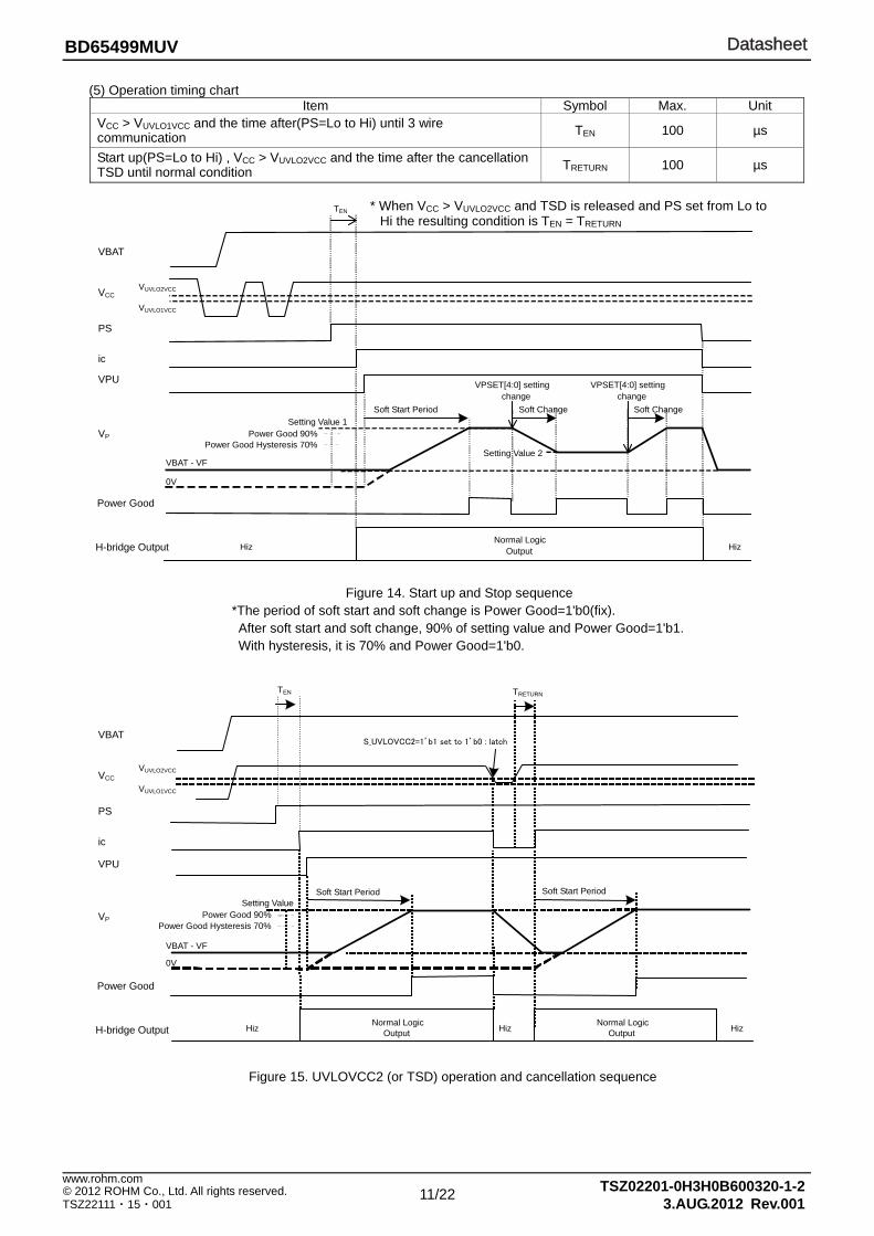
(5) Operation timing chart Item Symbol Max. Unit
VCC > VUVLO1VCC and the time after(PS=Lo to Hi) until 3 wire communication TEN 100 µs
Start up(PS=Lo to Hi) , VCC > VUVLO2VCC and the time after the cancellation TSD until normal condition TRETURN 100 µs
Figure 14. Start up and Stop sequence *The period of soft start and soft change is Power Good=1'b0(fix). After soft start and soft change, 90% of setting value and Power Good=1'b1. With hysteresis, it is 70% and Power Good=1'b0.
Figure 15. UVLOVCC2 (or TSD) operation and cancellation sequence
Power Good 90%
VPSET[4:0] settingchange
Normal Logic Output
Soft Start Period Soft Change Soft Change
HizHiz
Setting Value 1
Setting Value 2
VPSET[4:0] setting change
H-bridge Output
Power Good 0V VBAT - VF
VP
VPU ic
PS
VCC
VBAT
VUVLO2VCC
TEN
VUVLO1VCC
* When VCC > VUVLO2VCC and TSD is released and PS set from Lo toHi the resulting condition is TEN = TRETURN
Power Good Hysteresis 70%
Normal Logic Output
Soft Start Period
HizHiz Normal Logic Output Hiz
Soft Start Period
TRETURN
S_UVLOVCC2=1’b1 set to 1’b0 : latch
H-bridge Output
Power Good
0V VBAT - VF
VP
VPU
ic
PS
VCC
VBAT
Power Good 90% Setting Value
Power Good Hysteresis 70%
TEN
VUVLO2VCC VUVLO1VCC

DatasheetDatasheet
12/22 TSZ02201-0H3H0B600320-1-2© 2012 ROHM Co., Ltd. All rights reserved.
3.AUG.2012 Rev.001
www.rohm.com
TSZ22111・15・001
BD65499MUV
(6) AMPOUT terminal over voltage protection circuit
1. Monitoring AMPOUT voltage, And when it reach more than 1.8V, it make Class-A Amp output Pch. CMOS(M1) OFF and stop the energy supply from VCC.
2. Because the constant current I is active, it decrease the voltage in high value of AMPOUT toward GND direction. 3. It returns when the voltage of AMPOUT is less than 1.8V(typ.)
(7) In the case of amplifier unused
Use with connecting INN = AMPOUT terminal, and INP = GND.
AMPOVP AMPOUT1.8V over voltage protection
0 OFF (Default)
1 ON
Figure 16. Over voltage protection circuit of AMP block
AMPOUT
OVP 1.8V
1.8Vref
Amp
ControlPower Save
INP INN
VCC
M1
I=0.3mA typ.
AMPOVP
DatasheetDatasheet
13/22 TSZ02201-0H3H0B600320-1-2© 2012 ROHM Co., Ltd. All rights reserved.
3.AUG.2012 Rev.001
www.rohm.com
TSZ22111・15・001
BD65499MUV
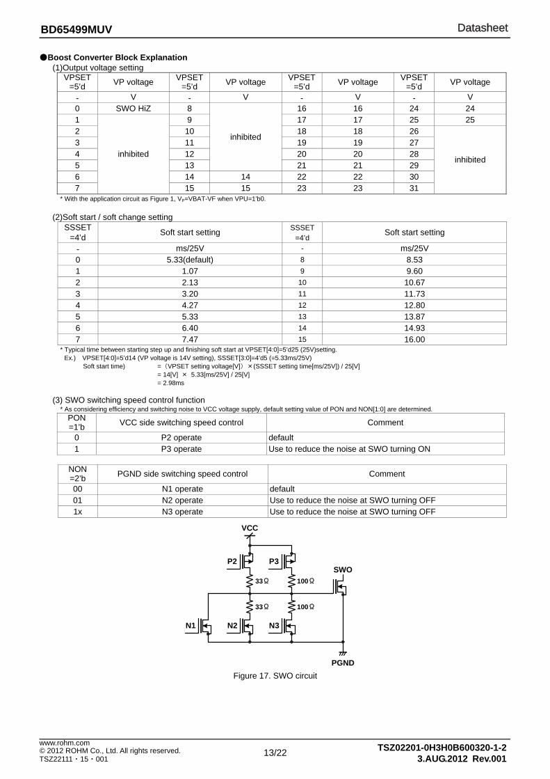
Boost Converter Block Explanation (1)Output voltage setting
VPSET =5’d VP voltage VPSET
=5’d VP voltage VPSET=5’d VP voltage VPSET
=5’d VP voltage
- V - V - V - V 0 SWO HiZ 8
inhibited
16 16 24 24 1
inhibited
9 17 17 25 25 2 10 18 18 26
inhibited
3 11 19 19 27 4 12 20 20 28 5 13 21 21 29 6 14 14 22 22 30 7 15 15 23 23 31
* With the application circuit as Figure 1, VP=VBAT-VF when VPU=1’b0.
(2)Soft start / soft change setting SSSET
=4’d Soft start setting SSSET=4’d Soft start setting
- ms/25V - ms/25V 0 5.33(default) 8 8.53 1 1.07 9 9.60 2 2.13 10 10.67 3 3.20 11 11.73 4 4.27 12 12.80 5 5.33 13 13.87 6 6.40 14 14.93 7 7.47 15 16.00
* Typical time between starting step up and finishing soft start at VPSET[4:0]=5’d25 (25V)setting. Ex.) VPSET[4:0]=5’d14 (VP voltage is 14V setting), SSSET[3:0]=4’d5 (=5.33ms/25V)
Soft start time) =(VPSET setting voltage[V])×(SSSET setting time[ms/25V]) / 25[V] = 14[V] × 5.33[ms/25V] / 25[V] = 2.98ms
(3) SWO switching speed control function
* As considering efficiency and switching noise to VCC voltage supply, default setting value of PON and NON[1:0] are determined. PON =1’b VCC side switching speed control Comment
0 P2 operate default 1 P3 operate Use to reduce the noise at SWO turning ON
NON =2’b PGND side switching speed control Comment
00 N1 operate default 01 N2 operate Use to reduce the noise at SWO turning OFF 1x N3 operate Use to reduce the noise at SWO turning OFF
Figure 17. SWO circuit
VCC
33Ω
33Ω
P2
100Ω
P3
100Ω
N3N2
PGND
SWO
N1
DatasheetDatasheet
14/22 TSZ02201-0H3H0B600320-1-2© 2012 ROHM Co., Ltd. All rights reserved.
3.AUG.2012 Rev.001
www.rohm.com
TSZ22111・15・001
BD65499MUV
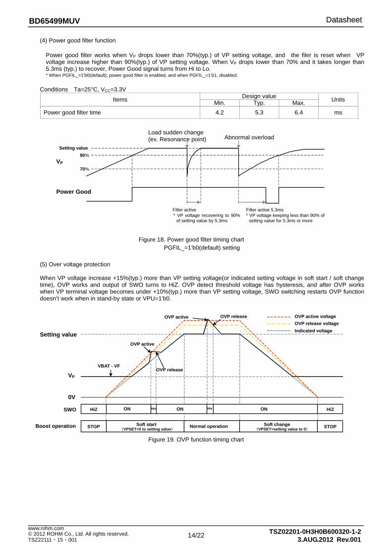
(4) Power good filter function
Power good filter works when VP drops lower than 70%(typ.) of VP setting voltage, and the filer is reset when VP voltage increase higher than 90%(typ.) of VP setting voltage. When VP drops lower than 70% and it takes longer than 5.3ms (typ.) to recover, Power Good signal turns from Hi to Lo. * When PGFIL_=1’b0(default), power good filter is enabled, and when PGFIL_=1’b1, disabled.
Conditions Ta=25°C, VCC=3.3V
Items Design value Units Min. Typ. Max. Power good filter time 4.2 5.3 6.4 ms
(5) Over voltage protection
When VP voltage increase +15%(typ.) more than VP setting voltage(or indicated setting voltage in soft start / soft change time), OVP works and output of SWO turns to HiZ. OVP detect threshold voltage has hysteresis, and after OVP works when VP terminal voltage becomes under +10%(typ.) more than VP setting voltage, SWO switching restarts OVP function doesn’t work when in stand-by state or VPU=1’b0.
Figure 19. OVP function timing chart
Load sudden change (ex. Resonance point)
Setting value 90%
70%
Power Good
Filter active* VP voltage recovering to 90%
of setting value by 5.3ms
VP
Abnormal overload
Filter active 5.3ms * VP voltage keeping less than 90% of
setting value for 5.3ms or more
VP
SWO ON HiZ HiZ
Boost operation Soft start (VPSET=0 to setting value)
STOP Normal operation Soft change (VPSET=setting value to 0) STOP
Hiz ONON
0V
Setting value
VBAT - VF
OVP active
OVP release
OVP active voltageOVP release voltageIndicated voltage
OVP active OVP release
Hiz
Figure 18. Power good filter timing chart PGFIL_=1’b0(default) setting

DatasheetDatasheet
15/22 TSZ02201-0H3H0B600320-1-2© 2012 ROHM Co., Ltd. All rights reserved.
3.AUG.2012 Rev.001
www.rohm.com
TSZ22111・15・001
BD65499MUV
H-bridge Block (1) H-bridge input and output truth table
Input method
INPUT OUTPUT PS*9 MODE INA INB OUTA OUTB Output mode
EN/IN
H
0 (default)
L X L L Short brakeH L H L ForwardH H L H Reverse
IN/IN 1
L L Z Z Open(default)H L H L ForwardL H L H ReverseH H L L Short brake
- L X X X Z Z OpenL; Low, H; High, X; Don’t care, Z; Hi impedance *9 PS terminal input logic High; IC active condition, Low; IC stand-by condition
(2) Output switching speed Condition Ta=25°C, VCC=3.3V, VP=20V, Load 100Ω Unit; ns
TR Turn On Time (TON)
Turn Off Time(TOFF)
Rise Time(TR)
Fall Time (TF)
Dead Time(Dead Time)
1’h0 300 50 350 20 801’h1 150 50 50 20 70
* Dead Time in generated by internal timer. * Rise Time and Fall Time are defined by the ability of pre-driver of H-bridge.
Control input
Output current
Dead Time
T F
T IN
- 10 % - 50 %
- 90 %
1 .45V
1.0V
0.5V
- 100%
0%
100%90%
50 % 10 %
90%
50%
10%-10%
-50 % - 90 %
TOFF
TON
DeadTime
TF TRT R
T OFF
TON
TIN
Figure 20. Definition of input-output AC characteristic

DatasheetDatasheet
16/22 TSZ02201-0H3H0B600320-1-2© 2012 ROHM Co., Ltd. All rights reserved.
3.AUG.2012 Rev.001
www.rohm.com
TSZ22111・15・001
BD65499MUV
3-wired Serial (1) 3-wired serial communication spec
Mode PS SEN SCLK SDATA
Stand-by mode Lo Input disable Input disable Input disable
Invalid communication mode Hi Hi Input disable Input disable
Write mode Hi Lo SDATA latch in a rising edge Data latch
* Input SCLK=Lo when VCC > VUVLO1VCC or the time between start up (PS=Lo to Hi) and 3-wired serial communication (TEN ).
Item Symbol Min. UnitSCLK period TCK 200 nsSCLK high pulse width TCKH 80 nsSCLK low pulse width TCKL 80 nsSEN START set up time TSENS 120 nsSEN END set up time TSENE 120 nsSTROBE high time TSH 300 nsDATA set up time (DATA of from SCLK falling to rising) TDS 80 nsDATA hold time (DATA of from SCLK rising to falling) TDH 80 ns
(2) Register map
ADDR W6 W5 W4 W3 W2 W1 W0 D7 D6 D5 D4 D3 D2 D1 D0
0 0 0 0 0 0 0 0 STATESET
STATESEL[2]
STATESEL[1]
STATESEL[0]
CLCAN CEL MODE LSET VPU
1 0 0 0 0 0 0 1 PON NON[1] NON[0] VPSET[4]
VPSET [3]
VPSET [2]
VPSET[1]
VPSET[0]
2 0 0 0 0 0 1 0 AMPOVP TEST TR TEST SSSET
[3] SSSET
[2] SSSET
[1] SSSET
[0] 3 0 0 0 0 0 1 1 TEST TEST TEST TEST TEST TEST TEST TEST
4 0 0 0 0 1 0 0 TEST TEST TEST TEST TEST TEST TEST TEST
5 0 0 0 0 1 0 1 TEST TEST PGFIL_ TEST TEST TEST TEST TEST* All value of default value is 0. Stand-by condition (PS=Lo) or VCC < VUVLO1VCC condition does reset the data as the default And all bits are set as 0.
* TEST Bits and other than address 0 to 2 should be set as 0(default) anytime.
67 45 23 01 67 45 23 01
7BIT ADDR
MSB
TSENS TCKH
TCKL
TCK TDS
TDH
TSENE TSH
SDATA
SCLK
SEN
MSB
Figure 21. 3-wired serial communication
DatasheetDatasheet
17/22 TSZ02201-0H3H0B600320-1-2© 2012 ROHM Co., Ltd. All rights reserved.
3.AUG.2012 Rev.001
www.rohm.com
TSZ22111・15・001
BD65499MUV
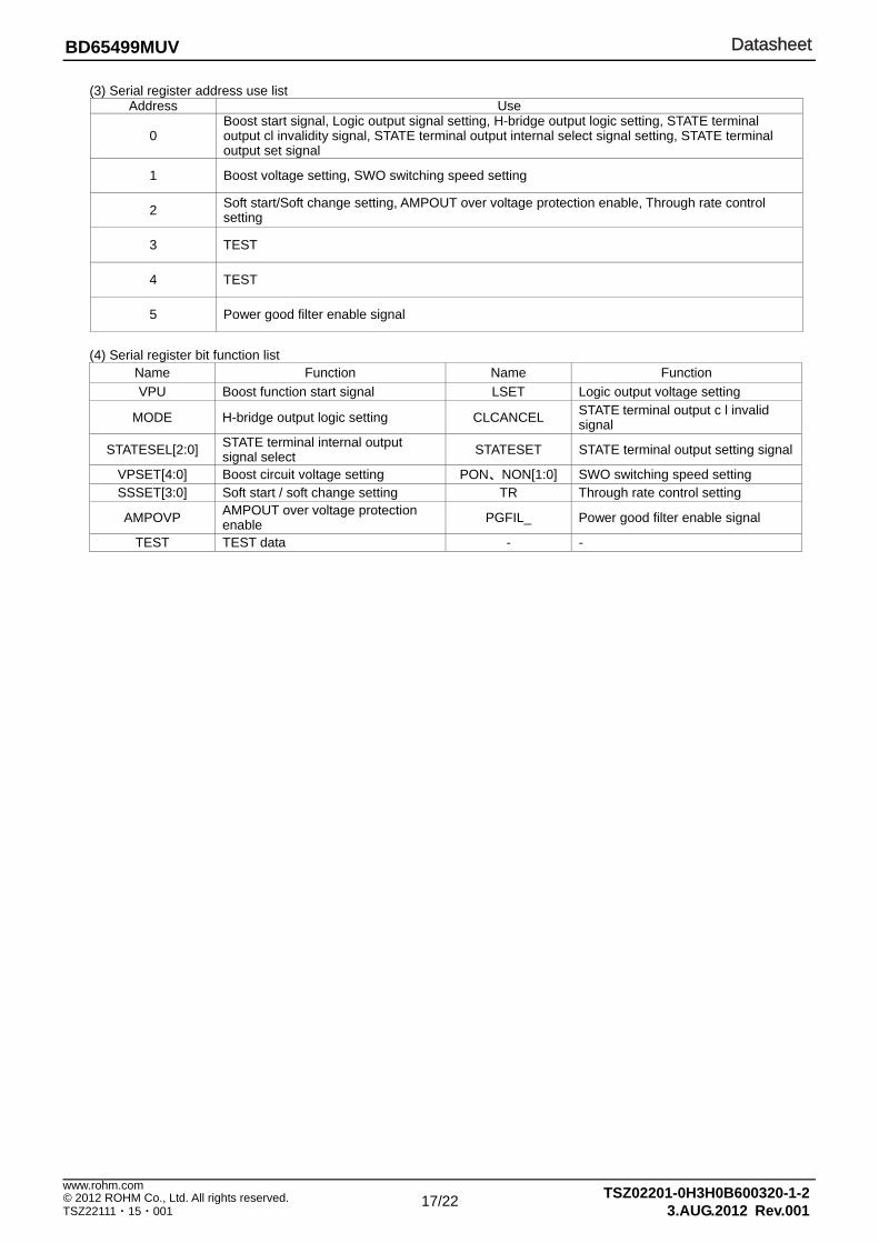
(3) Serial register address use list Address Use
0 Boost start signal, Logic output signal setting, H-bridge output logic setting, STATE terminal output cl invalidity signal, STATE terminal output internal select signal setting, STATE terminal output set signal
1 Boost voltage setting, SWO switching speed setting
2 Soft start/Soft change setting, AMPOUT over voltage protection enable, Through rate control setting
3 TEST
4 TEST
5 Power good filter enable signal
(4) Serial register bit function list
Name Function Name Function VPU Boost function start signal LSET Logic output voltage setting
MODE H-bridge output logic setting CLCANCEL STATE terminal output c l invalid signal
STATESEL[2:0] STATE terminal internal output signal select STATESET STATE terminal output setting signal
VPSET[4:0] Boost circuit voltage setting PON、NON[1:0] SWO switching speed setting SSSET[3:0] Soft start / soft change setting TR Through rate control setting
AMPOVP AMPOUT over voltage protection enable PGFIL_ Power good filter enable signal
TEST TEST data - -
DatasheetDatasheet
18/22 TSZ02201-0H3H0B600320-1-2© 2012 ROHM Co., Ltd. All rights reserved.
3.AUG.2012 Rev.001
www.rohm.com
TSZ22111・15・001
BD65499MUV
Power Dissipation
0
1000
2000
3000
4000
5000
0 25 50 75 100 125 150
Ambient temperature : Ta [°C]
Pow
er d
issi
patio
n : P
d [m
W]
Figure 22. Package heat reduction characteristic
4560mW
3260mW
880mW
85°C
2376mW
1700mW
460mW
DatasheetDatasheet
19/22 TSZ02201-0H3H0B600320-1-2© 2012 ROHM Co., Ltd. All rights reserved.
3.AUG.2012 Rev.001
www.rohm.com
TSZ22111・15・001
BD65499MUV
I/O Equivalence Circuits PS SCLK, SDATA, SEN, INA, INB STATE
SWO, PGND ERRIN, ERROUT VP, OUTA, OUTB, PGND
INP, INN AMPOUT VCC, N.C.
Figure 23. I/O equivalence circuit
ERROUT
ERRIN
PS
SCLKSDATASENINAINB STATE
PGND
SWO
INP INN
AMPOUT
VCC
N.C.
GND
OUTA
PGND
OUTB
VP

DatasheetDatasheet
20/22 TSZ02201-0H3H0B600320-1-2© 2012 ROHM Co., Ltd. All rights reserved.
3.AUG.2012 Rev.001
www.rohm.com
TSZ22111・15・001
BD65499MUV
Operational Notes 1) Absolute maximum ratings
Use of the IC in excess of absolute maximum ratings such as the applied voltage or operating temperature range may result in IC damage. Assumptions should not be made regarding the state of the IC (short mode or open mode) when such damage is suffered. The implementation of a physical safety measure such as a fuse should be considered when use of the IC in a special mode where the absolute maximum ratings may be exceeded is anticipated.
2) Power supply pins and lines None of the VP line for the H-bridges is internally connected to the VCC power supply line, which is only for the control logic or analog circuit. Therefore, the VP and VCC lines can be driven at different voltages. Although these lines can be connected to a common power supply, do not open the power supply pin but connect it to the power supply externally. Regenerated current may flow as a result of the motor's back electromotive force. Insert capacitors between the power supply and ground pins to serve as a route for regenerated current. Determine the capacitance in full consideration of all the characteristics of the electrolytic capacitor, because the electrolytic capacitor may loose some capacitance at low temperatures. If the connected power supply does not have sufficient current absorption capacity, regenerative current will cause the voltage on the power supply line to rise, which combined with the product and its peripheral circuitry may exceed the absolute maximum ratings. It is recommended to implement a physical safety measure such as the insertion of a voltage clamp diode between the power supply and ground pins. For this IC with several power supplies and a part consists of the CMOS block, it is possible that rush current may flow instantaneously due to the internal powering sequence and delays, and to the unstable internal logic, respectively. Therefore, give special consideration to power coupling capacitance, width of power and ground wirings, and routing of wiring.
3) Ground pins and lines Ensure a minimum GND pin potential in all operating conditions. Make sure that no pins are at a voltage below the GND at any time, regardless of whether it is a transient signal or not. When using both small signal GND and large current PGND patterns, it is recommended to isolate the two ground patterns, placing a single ground point at the application's reference point so that the pattern wiring resistance and voltage variations caused by large currents do not cause variations in the small signal ground voltage. Be careful not to change the GND wiring pattern of any external components, either. The power supply and ground lines must be as short and thick as possible to reduce line impedance.
4) Thermal design Use a thermal design that allows for a sufficient margin in light of the power dissipation (Pd) in actual operating conditions.
5) Actions in strong magnetic field Use caution when using the IC in the presence of a strong magnetic field as doing so may cause the IC to malfunction.
6) ASO
When using the IC, set the output transistor for the motor so that it does not exceed absolute maximum ratings or ASO.
7) Thermal shutdown circuit This IC incorporates a TSD (thermal shutdown) circuit. If the temperature of the chip reaches the following temperature, the motor coil output will be opened. The TSD circuit is designed only to shut the IC off to prevent runaway thermal operation. It is not designed to protect the IC or guarantee its operation. Do not continue to use the IC after operating this circuit or use the IC in an environment where the operation of this circuit is assumed.
TSD ON temperature [°C] (Typ.) Hysteresis temperature [°C] (Typ.)
175 20
8) After releasing Under Voltage Locked Out (UVLO) or Thermal Shut Down (TSD) When UVLO, TSD is released, it returns normal operation after 100µs (max).
9) VBAT external power supply
This IC is not equipped with terminal of VBAT, and operate even the VBAT external power supply is lower than 4V (minimum VP operation voltage). Give consideration that if VBAT external power supply is low and VP setting voltage is high or load is large, may cause an overcurrent flowing through SWO terminal, and may enable OCP, TSD, etc. In addition, if the VBAT external power supply has changed during the boost operation (ex. VBAT=HiZ), because of boosting VP to setting voltage without working soft start / soft change, may cause overcurrent flowing through SWO terminal. If VBAT external power supply is changing, stop boost operation by setting PS=0V or VPU=1’b0, then set the soft start function after VBAT power supply voltage is stable.
10) N.C. pin
Always keep N.C. pin open.
DatasheetDatasheet
21/22 TSZ02201-0H3H0B600320-1-2© 2012 ROHM Co., Ltd. All rights reserved.
3.AUG.2012 Rev.001
www.rohm.com
TSZ22111・15・001
BD65499MUV
11) Application example The application circuit is recommended for use. Make sure to confirm the adequacy of the characteristics. When using the circuit with changes to the external circuit constants, make sure to leave an adequate margin for external components including static and transitional characteristics as well as dispersion of the IC.
Status of this document The Japanese version of this document is formal specification. A customer may use this translation version only for a reference to help reading the formal version. If there are any differences in translation version of this document formal version takes priority Physical Dimension, Tape and Reel Information Marking Diagram
VQFN028V5050 (TOP VIEW)
D 6 5 4 9 9
Part Number Marking
LOT Number
1PIN MARK
Figure 24. Example of Simple IC Architecture
(Unit : mm)
VQFN028V5050
0.08 S
S
1PIN MARK
1 7
8
1422
28
1521
0.4±
0.1
1.0 0.5 0.25+0.05-0.04
2.7±0.1
2.7±
0.1
C0.2
5.0±
0.1
5.0±0.1
0.02
+0.
03-0
.02
(0.2
2)1.0M
AX
∗ Order quantity needs to be multiple of the minimum quantity.
<Tape and Reel information>
Embossed carrier tapeTape
Quantity
Direction of feed
The direction is the 1pin of product is at the upper left when you hold reel on the left hand and you pull out the tape on the right hand
2500pcs
E2
( )
Direction of feed
Reel1pin
Parasitic element Other adjacent elements
Parasitic element
N
N N P+ P+ P
P substrate
GND
Pin A
N
N P+ P+ P
P substrate
GND
Parasitic element
Pin B C
B
E
N
GND
Pin A
Parasitic element
Pin B
E
B C
GND
Resistor Transistor (NPN)

DatasheetDatasheet
22/22 TSZ02201-0H3H0B600320-1-2© 2012 ROHM Co., Ltd. All rights reserved.
3.AUG.2012 Rev.001
www.rohm.com
TSZ22111・15・001
BD65499MUV
Revision History Date Revision Changes
3.Aug.2012 001 New Release
DatasheetDatasheet
Notice - GE Rev.002© 2014 ROHM Co., Ltd. All rights reserved.
Notice Precaution on using ROHM Products
1. Our Products are designed and manufactured for application in ordinary electronic equipments (such as AV equipment, OA equipment, telecommunication equipment, home electronic appliances, amusement equipment, etc.). If you intend to use our Products in devices requiring extremely high reliability (such as medical equipment (Note 1), transport equipment, traffic equipment, aircraft/spacecraft, nuclear power controllers, fuel controllers, car equipment including car accessories, safety devices, etc.) and whose malfunction or failure may cause loss of human life, bodily injury or serious damage to property (“Specific Applications”), please consult with the ROHM sales representative in advance. Unless otherwise agreed in writing by ROHM in advance, ROHM shall not be in any way responsible or liable for any damages, expenses or losses incurred by you or third parties arising from the use of any ROHM’s Products for Specific Applications.
(Note1) Medical Equipment Classification of the Specific Applications JAPAN USA EU CHINA
CLASSⅢ CLASSⅢ
CLASSⅡb CLASSⅢ
CLASSⅣ CLASSⅢ
2. ROHM designs and manufactures its Products subject to strict quality control system. However, semiconductor
products can fail or malfunction at a certain rate. Please be sure to implement, at your own responsibilities, adequate safety measures including but not limited to fail-safe design against the physical injury, damage to any property, which a failure or malfunction of our Products may cause. The following are examples of safety measures:
[a] Installation of protection circuits or other protective devices to improve system safety [b] Installation of redundant circuits to reduce the impact of single or multiple circuit failure
3. Our Products are designed and manufactured for use under standard conditions and not under any special or extraordinary environments or conditions, as exemplified below. Accordingly, ROHM shall not be in any way responsible or liable for any damages, expenses or losses arising from the use of any ROHM’s Products under any special or extraordinary environments or conditions. If you intend to use our Products under any special or extraordinary environments or conditions (as exemplified below), your independent verification and confirmation of product performance, reliability, etc, prior to use, must be necessary:
[a] Use of our Products in any types of liquid, including water, oils, chemicals, and organic solvents [b] Use of our Products outdoors or in places where the Products are exposed to direct sunlight or dust [c] Use of our Products in places where the Products are exposed to sea wind or corrosive gases, including Cl2,
H2S, NH3, SO2, and NO2
[d] Use of our Products in places where the Products are exposed to static electricity or electromagnetic waves [e] Use of our Products in proximity to heat-producing components, plastic cords, or other flammable items [f] Sealing or coating our Products with resin or other coating materials [g] Use of our Products without cleaning residue of flux (even if you use no-clean type fluxes, cleaning residue of
flux is recommended); or Washing our Products by using water or water-soluble cleaning agents for cleaning residue after soldering
[h] Use of the Products in places subject to dew condensation
4. The Products are not subject to radiation-proof design. 5. Please verify and confirm characteristics of the final or mounted products in using the Products. 6. In particular, if a transient load (a large amount of load applied in a short period of time, such as pulse. is applied,
confirmation of performance characteristics after on-board mounting is strongly recommended. Avoid applying power exceeding normal rated power; exceeding the power rating under steady-state loading condition may negatively affect product performance and reliability.
7. De-rate Power Dissipation (Pd) depending on Ambient temperature (Ta). When used in sealed area, confirm the actual
ambient temperature. 8. Confirm that operation temperature is within the specified range described in the product specification. 9. ROHM shall not be in any way responsible or liable for failure induced under deviant condition from what is defined in
this document.
Precaution for Mounting / Circuit board design 1. When a highly active halogenous (chlorine, bromine, etc.) flux is used, the residue of flux may negatively affect product
performance and reliability. 2. In principle, the reflow soldering method must be used; if flow soldering method is preferred, please consult with the
ROHM representative in advance. For details, please refer to ROHM Mounting specification

DatasheetDatasheet
Notice - GE Rev.002© 2014 ROHM Co., Ltd. All rights reserved.
Precautions Regarding Application Examples and External Circuits 1. If change is made to the constant of an external circuit, please allow a sufficient margin considering variations of the
characteristics of the Products and external components, including transient characteristics, as well as static characteristics.
2. You agree that application notes, reference designs, and associated data and information contained in this document
are presented only as guidance for Products use. Therefore, in case you use such information, you are solely responsible for it and you must exercise your own independent verification and judgment in the use of such information contained in this document. ROHM shall not be in any way responsible or liable for any damages, expenses or losses incurred by you or third parties arising from the use of such information.
Precaution for Electrostatic
This Product is electrostatic sensitive product, which may be damaged due to electrostatic discharge. Please take proper caution in your manufacturing process and storage so that voltage exceeding the Products maximum rating will not be applied to Products. Please take special care under dry condition (e.g. Grounding of human body / equipment / solder iron, isolation from charged objects, setting of Ionizer, friction prevention and temperature / humidity control).
Precaution for Storage / Transportation 1. Product performance and soldered connections may deteriorate if the Products are stored in the places where:
[a] the Products are exposed to sea winds or corrosive gases, including Cl2, H2S, NH3, SO2, and NO2 [b] the temperature or humidity exceeds those recommended by ROHM [c] the Products are exposed to direct sunshine or condensation [d] the Products are exposed to high Electrostatic
2. Even under ROHM recommended storage condition, solderability of products out of recommended storage time period may be degraded. It is strongly recommended to confirm solderability before using Products of which storage time is exceeding the recommended storage time period.
3. Store / transport cartons in the correct direction, which is indicated on a carton with a symbol. Otherwise bent leads
may occur due to excessive stress applied when dropping of a carton. 4. Use Products within the specified time after opening a humidity barrier bag. Baking is required before using Products of
which storage time is exceeding the recommended storage time period.
Precaution for Product Label QR code printed on ROHM Products label is for ROHM’s internal use only.
Precaution for Disposition When disposing Products please dispose them properly using an authorized industry waste company.
Precaution for Foreign Exchange and Foreign Trade act Since our Products might fall under controlled goods prescribed by the applicable foreign exchange and foreign trade act, please consult with ROHM representative in case of export.
Precaution Regarding Intellectual Property Rights 1. All information and data including but not limited to application example contained in this document is for reference
only. ROHM does not warrant that foregoing information or data will not infringe any intellectual property rights or any other rights of any third party regarding such information or data. ROHM shall not be in any way responsible or liable for infringement of any intellectual property rights or other damages arising from use of such information or data.:
2. No license, expressly or implied, is granted hereby under any intellectual property rights or other rights of ROHM or any
third parties with respect to the information contained in this document.
Other Precaution 1. This document may not be reprinted or reproduced, in whole or in part, without prior written consent of ROHM. 2. The Products may not be disassembled, converted, modified, reproduced or otherwise changed without prior written
consent of ROHM. 3. In no event shall you use in any way whatsoever the Products and the related technical information contained in the
Products or this document for any military purposes, including but not limited to, the development of mass-destruction weapons.
4. The proper names of companies or products described in this document are trademarks or registered trademarks of
ROHM, its affiliated companies or third parties.

DatasheetDatasheet
Notice – WE Rev.001© 2014 ROHM Co., Ltd. All rights reserved.
General Precaution 1. Before you use our Pro ducts, you are requested to care fully read this document and fully understand its contents.
ROHM shall n ot be in an y way responsible or liabl e for fa ilure, malfunction or acci dent arising from the use of a ny ROHM’s Products against warning, caution or note contained in this document.
2. All information contained in this docume nt is current as of the issuing date and subj ect to change without any prior
notice. Before purchasing or using ROHM’s Products, please confirm the la test information with a ROHM sale s representative.
3. The information contained in this doc ument is provi ded on an “as is” basis and ROHM does not warrant that all
information contained in this document is accurate an d/or error-free. ROHM shall not be in an y way responsible or liable for any damages, expenses or losses incurred by you or third parties resulting from inaccuracy or errors of or concerning such information.