draft dual-mode wpc/pma 5 watt wireless power receiver ic
TRANSCRIPT

DRAFT
Dual-Mode WPC/PMA 5 Watt Wireless Power Receiver IC
P9028AC Product Datasheet
Revision 1.0.3 1 © 2015 Integrated Device Technology, Inc.
Features Single Chip Receiver (Rx) Solution WPC v1.1.2 Compliant PMA v1, v3 Pre-Release Compatible with Options Advanced WPC v1.1.2 Foreign Object Detection (FOD) Programmable FOD setting via external resistor and
I2C registers Programmable current limit via external resistor Integrated Full-Bridge Synchronous Rectifier Integrated 5V @ 1A LDO Regulator Output Closed-loop power transfer control between TX and
RX I2C interface provides VRECT, Iout and switching
frequency values Open-Drain LED Indicator Output Over-Temperature/Voltage/Current Protection
Applications WPC-Compliant and PMA-Compatible Wireless
Chargers for Mobile Applications. Cellular Mobile Phones Tablets, DSC, DVC and Handhelds
Introduction The P9028AC is an integrated single-chip, dual-mode WPC v1.1.2-compliant and PMA v1.0-compatible, wireless power receiver IC with advanced WPC v1.1.2 Foreign Object Detection (FOD). The device operates with an AC power signal from a resonant tank and converts it into a regulated 5V output voltage, which can be used to supply power to a mobile application. It includes a high efficiency Synchronous Full Bridge Rectifier and 5V tracking LDO output stage. The P9028AC dual-mode operation automatically detects the transmitter type and initiates either WPC or PMA AC modulation communication protocols with optimal efficiency. The device includes the control circuit required to modulate the load to transmit WPC-compliant or PMA-compatible message packets to the base station. It uses minimal external components to reduce overall solution area. The P9028AC employs advanced programmable WPC FOD techniques to detect foreign metallic objects placed on the transmitter base station derived from a transmitted and received power transfer algorithm. The P9028AC is available in a 36 ball 3mm X 3mm WLCSP or 32 pin 5mm X 5mm TQFN package.
Typical Application Circuit
Packages: WLCSP-36 6x6 balls (3.06mm x 2.9mm) (See page 33)
TQFN-32 5x5mm (See page 35) Ordering information: (See page 38)

P9028AC
Product Datasheet
Revision 1.0.3 2 © 2015 Integrated Device Technology, Inc.
SIMPLIFIED APPLICATION DIAGRAM
Figure 1. Simplified Applications Schematic.

P9028AC
Product Datasheet
Revision 1.0.3 3 © 2015 Integrated Device Technology, Inc.
ABSOLUTE MAXIMUM RATINGS These absolute maximum ratings are stress ratings only. Stresses greater than those listed below (Table 1 and Table 2) may cause permanent damage to the device. Functional operation of the P9028AC at absolute maximum ratings is not implied. Application of the absolute maximum rating conditions affects device reliability.
Table 1. Absolute Maximum Ratings Summary.
Description Value Units
AC1, AC2, VRECT, ACM1, ACM2, CLAMP1, CLAMP2 -0.3 to 20 V
BST1, BST2 -0.3 to (AC1, AC2 + 6) V
EN, STAT, SCL, SDA, OUT, SNS, TEOP, RLIM, CS100, FOD1, FOD2, VDD -0.3 to 6 V
PGND, PGND1, PGND2, AGND -0.3 to 0.3 V
Output Current OUT 1.5 A
Input Current AC1, AC2 2 ARMS
Table 2. Package Thermal Information.1,2,3,4
Symbol Description TQFN Rating WLCSP Rating
(7 thermal vias) Units
JA Thermal Resistance Junction to Ambient 35 70 C/W
JC Thermal Resistance Junction to Case 29.6 0.9 C/W
JB Thermal Resistance Junction to Board 2.4 47.3 C/W
TJ Operating Junction Temperature 0 to +125 0 to +125 C
TA Operating Ambient Temperature 0 to +85 0 to +85 C
TSTG Storage Temperature -55 to +150 -55 to +150 C
TLEAD Maximum Soldering Temperature (at Leads, 10s) 300 300 C
Note 1: The maximum power dissipation is PD(MAX) = (TJ(MAX) - TA) / θJA where TJ(MAX) is 125°C. Exceeding the maximum allowable power dissipation will result in excessive die temperature, and the device will enter thermal shutdown.
Note 2: This thermal rating was calculated on JEDEC 51 standard 4-layer board with dimensions 3” x 4.5” in still air conditions.
Note 3: Actual thermal resistance is affected by PCB size, solder joint quality, layer count, copper thickness, air flow, altitude, and other unlisted variables. Note 4: For the NBG32 package, connecting the 5 mm X 5 mm EP to internal/external ground planes with a 5x5 matrix of PCB plated-through-hole (PTH) vias, from top to bottom sides of the PCB, is recommended for improving the overall thermal performance. For the WLCSP (AWG36) package, connecting the 7 thermal balls to internal/external ground planes from top to bottom sides of the PCB, is recommended for improving the overall thermal performance.
Table 3. ESD Information.
Test Model
Pins Rating Units
HBM All ±1500 V
CDM All ±500 V

P9028AC
Product Datasheet
Revision 1.0.3 4 © 2015 Integrated Device Technology, Inc.
ELECTRICAL SPECIFICATION TABLE VRECT=6V, COUT=1uF, CVRECT=20uF, VEN=0V, TA = 0C to 85C, unless otherwise noted. Typical values are at 25°C, unless otherwise noted.
Table 4. Device Characteristics.
Symbol Description Conditions Min Typ Max Units
Under-voltage Lock-out
VUVLO Under-voltage lockout Rising voltage on VRECT 2.3 2.5 2.7 V
VUVLO-HYS UVLO hysteresis 50 mV Over-voltage Protection
VOVP Over-voltage VRECT Rising voltage on VRECT 12.8 13.3 13.8 V VOVP-HYS Over-voltage hysteresis 1.5 V Power Supply Current
IRECT Quiescent current IOUT = 0mA, with internal load 14 16 18 mA IOUT = 0mA, no internal load 2 3 4 mA
Low-drop-out Regulator
ILIM Output current limit OUT
RLIM=30kΩ 1.15 1.6 1.95 A
RLIM<25KΩ (Note 1) 2.0
VOUT Regulated output voltage OUT
IOUT = 0mA to 1000mA 5.04 5.3 5.56 V
VDD Voltage (For Internal Supply Use Only)
VDD_INT Internal Supply Voltage IVDD = 100A, maximum allowable load for test purposes
4.44 4.54 4.64 V
Thermal Shutdown
TSHD Thermal shutdown threshold
Temperature rising 150 °C Temperature falling 130 °C
Digital Input and Output Characteristics
VIL Logic level input low EN, CS100, TEOP 0.4
V
VIH Logic level input high EN, CS100, TEOP 1.3
V
VOL Open drain voltage STAT, INT
ISTAT = 4mA 400 mV
RPD Pull-down resistance EN, CS100 200
kΩ TEOP 1000
Switch On-resistance
RDSON
ACM1, ACM2 switches
150mA
1600 mΩ CLAMP1, CLAMP2 switches
400 475 680 mΩ
Rectifier bridge switches 60 110 180 mΩ

P9028AC
Product Datasheet
Revision 1.0.3 5 © 2015 Integrated Device Technology, Inc.
ELECTRICAL SPECIFICATION TABLE VRECT=6V, COUT=1uF, CVRECT=20uF, VEN=0V, TA = 0C to 85C, unless otherwise noted. Typical values are at 25°C, unless otherwise noted.
Table 4. Device Characteristics (Continued).
Symbol Description Conditions Min Typ Max Units
SCL, SDA (I2C Interface) fSCL Clock Frequency 0 400 kHz tLOW Clock Low Period 1.3 µs tHIGH Clock High Period 0.6 µs
tHD,STA Hold Time (Repeated) for START Condition
0.6 µs
tSU:STA Set-up Time for Repeated START Condition
0.6 µs
tSU:DAT Data Setup Time 100 ns tHD:DAT Data Hold Time 0.9 µs
tSU:STO Setup Time for STOP Condition
0.6 µs
tBUF Bus Free Time Between STOP and START Condition
1.3 µs
tR Rise Time of Both SDA and SCL Signals (Note 1,2)
20 + 0.1 CB 300 ns
tF Fall Time of Both SDA and SCL Signals (Note 1,2) 20 + 0.1 CB 300 ns
TSP Spike Pulse Widths Suppressed by Input Filter (Note 1,2)
0 50 ns
CB Capacitive Load for Each Bus Line (Note 1,2)
400 pF
CBIN SCL, SDA Input Capacitance (Note 1,2)
60 pF
VIL Input Threshold Low 0.4 V VIH Input Threshold High 1.4 V II Input Leakage Current -1.0 1.0 µA
Note 1: Guaranteed by design. Not 100% tested in production. Note 2: Guaranteed by design/simulation data.

P9028AC
Product Datasheet
Revision 1.0.3 6 © 2015 Integrated Device Technology, Inc.
TYPICAL PERFORMANCE CHARACTERISTICS Typical Performance Characteristics: System Efficiency versus RX Output Power EN¯¯ = RESET = 0, TA = 25oC
0%
10%
20%
30%
40%
50%
60%
70%
80%
90%
0 0.5 1 1.5 2 2.5 3 3.5 4 4.5 5
Efficiency (%)
Output Power (W)
P9028AC System Efficiency (%) vs. Output Power (W)from IDTP9235 (WPC) or PMA Tx (1mm space)
IDTP9235PMA
Figure 2. P9028AC WPC and PMA System Efficiency.

P9028AC
Product Datasheet
Revision 1.0.3 7 © 2015 Integrated Device Technology, Inc.
Figure 3. P9028AC RX Startup-to-out waveforms from IDTP9235 TX, IOUT=0A, CH1=VRECT, CH2=VOUT, CH3=Rx coil Current, CH4=VDD.
Figure 4. P9028AC RX Startup-to-out waveforms from IDTP9235 TX, IOUT=1A, CH1=VRECT, CH2= VOUT, CH3=Rx coil Current, CH4=VDD.

P9028AC
Product Datasheet
Revision 1.0.3 8 © 2015 Integrated Device Technology, Inc.
Figure 5. P9028AC RX Startup-to-out waveforms from PMA TX, IOUT=0A, CH1= VOUT, CH2= VRECT, CH3= VDD, CH4= Rx coil Current.
Figure 6. P9028AC RX Startup-to-out waveforms from PMA TX, IOUT=0A, CH1= VOUT, CH2= VRECT, CH3= VDD, CH4= Rx coil Current.

P9028AC
Product Datasheet
Revision 1.0.3 9 © 2015 Integrated Device Technology, Inc.
PIN CONFIGURATION & DESCRIPTION
Figure 7. P9028AC WLCSP Pin Configuration (Top View).

P9028AC
Product Datasheet
Revision 1.0.3 10 © 2015 Integrated Device Technology, Inc.
Table 5. WLCSP Pin Descriptions.
Pin # Name Type Description
A1 CHG_END/CS100 I
Active-high input pin. Default setting is a Charge-End active-high input from an external battery charger to terminate power transfer. Alternatively, a Charge-Status active high input which will send a WPC Charge Status packet with value 100 (100% charge). In PMA mode, an End Of Charge (EOC) command will be sent. This pin has an internal pull down resistor.
A2 OUT_A2 O
5V LDO output. A 0.1μF ceramic capacitor and a 1μF to 10μF ceramic capacitor must be connected between this pin and ground. A3 OUT_A3
A4 EN I Active-low enable pin. If this pin is pulled high, the chip will send a WPC EOP packet with code 0x04 (over-voltage code) or a PMA EOC signal. This pin has an internal pull down resistor.
A5 CLAMP2_A5 I AC clamp input 2.
A6 CLAMP2_A6
B1 VRECT_B1 O Output of the full-wave rectifier.
B2 VRECT_B2
B3 RLIM I Current-limit resistor. A resistor connected between this pin and ground sets the current limit of the 5V LDO.
B4 TEOP I Active-high over-temperature input pin. If this pin is pulled high, the chip will send a WPC EOP packet with code 0x03 (over-temperature code) or a PMA EOC signal. This pin has an internal pull down resistor.
B5 PGND2_B5 - Power ground for the AC clamp FETs.
B6 PGND2_B6 C1 AC1_C1
I AC1 input to the Internal full-wave rectifier. C2 AC1_C2
C3 NC1 NC Not internally connected. This pin may be connected to ground to improve thermal performance or to other pins to facilitate routing.
C4 FOD2 I Foreign object detection 2 offset adjustment. C5 CLAMP1_C5
I AC clamp input 1. C6 CLAMP1_C6 D1 PGND_D1
- Power ground for the full-wave rectifier. D2 PGND_D2
D3 DNC1 DNC DO NOT connect to this pin, it is internally connected. This pin must be left floating.
D4 ACM1 I AC Modulation input 1. D5 AC2_D5
I AC2 input to the Internal full-wave rectifier. D6 AC2_D6 E1 BST2 O Bootstrap output for high-side rectifier FET 2. E2 BST1 O Bootstrap output for high-side rectifier FET 1.
E3 DNC2 DNC INTERNALLY CONNECTED. DO NOT connect to this pin. This pin must be left floating.
E4 SCL I I2C clock port. If not used, connect to ground. E5 ACM2 I AC Modulation input 2. E6 PGND1 - Power ground for modulation FETs.
F1 INT O Interrupt output. Open drain output pin. A low condition indicates that an OC, OV, or OT event has occurred.
F2 STAT O Status output (STAT . Open drain output pin. A low condition indicates that power is being transferred.
F3 VDD O Internal voltage supply. Connect a 1uF to 10uF capacitor between this pin and ground. Must be left unloaded.
F4 AGND - Analog ground connection. F5 SDA I/O I2C data port. If not used, connect to ground. F6 FOD1 I Foreign object detection 1 to select internal FOD1 settings.

P9028AC
Product Datasheet
Revision 1.0.3 11 © 2015 Integrated Device Technology, Inc.
PIN CONFIGURATION & DESCRIPTION (CONTINUED)
1
2
3
4
5
6
7
11 12 13 14 15 16
30 29 28 27 26 25
8
23
22
21
20
19
18
17
24INT
DNC1
DNC2
BST2
BST1
AC1
VRECT
RLIM
NC4
ACM2
PGND1
ACM1
FOD2
CLAMP1
PGND2
CLAMP2
AC
2
VD
D
AG
ND
SC
L
SD
A
FO
D1
NC
1
OU
T
NC
2
EN
TE
OP
NC
3
32 31
ST
AT
PG
ND
9 10
SN
S
CH
G_
EN
D/C
S10
0
EP
Figure 8. P9028AC TQFN32 5mm X 5mm Pin Configuration (Top View).

P9028AC
Product Datasheet
Revision 1.0.3 12 © 2015 Integrated Device Technology, Inc.
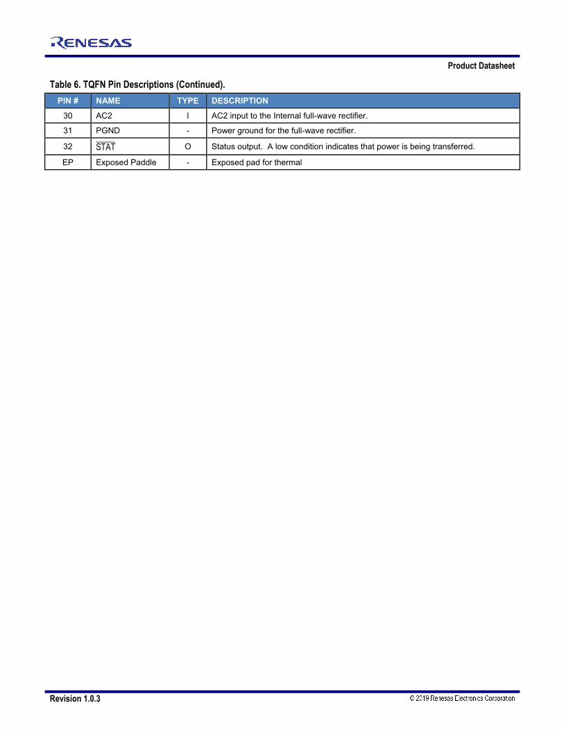
Table 6. TQFN Pin Descriptions.
Pin # Name Type Description
1 INT O Interrupt output. Open drain output pin. A low condition indicates that an OC, OV, or OT event has occurred.
2 DNC1 DNC DO NOT connect to this pin, it is internally connected. This pin must be left floating.
3 DNC2 DNC DO NOT connect to this pin, it is internally connected. This pin must be left floating.
4 BST2 O Bootstrap output for high-side rectifier FET 2.
5 BST1 O Bootstrap output for high-side rectifier FET 1.
6 AC1 I AC1 input to the Internal full-wave rectifier.
7 VRECT O Output of the full-wave rectifier.
8 RLIM I Current-limit resistor. A resistor connected between this pin and ground sets the current limit of the 5V LDO.
9 SNS I LDO output sense pin. Connect to the OUT pin (TQFN only).
10 CHG_END/CS100 I
Active-high input pin. Default setting is a Charge-End active-high input from an external battery charger to terminate power transfer. Alternatively, a Charge-Status active high input which will send a WPC Charge Status packet with value 100 (100% charge). In PMA mode, an End Of Charge (EOC) command will be sent. This pin has an internal pull down resistor.
11 NC1 NC Not internally connected. This pin may be connected to others to facilitate routing or to improve thermal performance.
12 OUT O 5V LDO output. A 1μF ceramic capacitor must be connected between this pin and ground.
13 NC2 NC Not internally connected. This pin may be connected to others to facilitate routing or to improve thermal performance.
14 EN I Active-low enable pin. The chip is suspended and placed in low-current (sleep) mode when pulled high. This pin is pulled low inside the chip.
15 TEOP I Active-high over-temperature input pin. If this pin is pulled high, the chip will send a WPC EOP packet with code 0x03 (over-temperature code) or a PMA EOC signal. This pin has an internal pull down resistor.
16 NC3 NC Not internally connected. This pin may be connected to others to facilitate routing or to improve thermal performance.
17 CLAMP2 I AC clamp input 2.
18 PGND2 - Power ground for the AC clamp FETs.
19 CLAMP1 I AC clamp input 1.
20 FOD2 I FOD2 adjustment
21 ACM1 I AC Modulation input 1.
22 PGND1 - Power ground for the full-wave rectifier.
23 ACM2 I AC Modulation input 2.
24 NC4 NC Not internally connected. This pin may be connected to others to facilitate routing or to improve thermal performance.
25 FOD1 I Select FOD settings
26 SDA I/O I2C data port. If not used, connect to ground.
27 SCL I I2C clock port. If not used, connect to ground.
28 AGND - Analog ground connection.
29 VDD O Internal voltage supply. Connect a 1uF to 10uFcapacitor between this pin and ground. Must be left unloaded.
P9028AC
Product Datasheet
Revision 1.0.3 13 © 2015 Integrated Device Technology, Inc.
Table 6. TQFN Pin Descriptions (Continued).
PIN # NAME TYPE DESCRIPTION
30 AC2 I AC2 input to the Internal full-wave rectifier.
31 PGND - Power ground for the full-wave rectifier.
32 STAT O Status output. A low condition indicates that power is being transferred.
EP Exposed Paddle - Exposed pad for thermal

P9028AC
Product Datasheet
Revision 1.0.3 14 © 2015 Integrated Device Technology, Inc.
FUNCTIONAL BLOCK DIAGRAM
PGND
Driver&
Control
Peripherals
STAT
I C SCL
SDA
GND
OTP + Digital
Multi Channel ADC with
Analog MUX and Digital
Control
OUT
VRECT
LDO5VControl
AC1
AC2
ACM1
ACM2
CLAMP1
CLAMP2
BST1
BST2
AC Modulation
and Overvoltage protection
GND
EN
Internal LDO
GND
4.5V
RLIMCurrent
limit control
EOPControl
TEOP
2
CS100
FOD1
FOD2
VDD
Interrupt Control
INT
VIN-UVLO
Figure 9. Simplified Internal Block Diagram.

P9028AC
Product Datasheet
Revision 1.0.3 15 © 2015 Integrated Device Technology, Inc.
DESCRIPTION OF THE WIRELESS POWER CHARGING SYSTEM A wireless power charging system has a base station with one or more transmitters that make power available via DC-to-AC inverter(s) and transmit the power over a strongly-coupled inductor pair to a receiver in a mobile device. A WPC1 transmitter may be a free-positioning or magnetically-guided type. PMA2 supports only the magnetically-guided configuration. A free-positioning type of transmitter has one coil or an array of coils that gives limited spatial freedom to the end-user, whereas a magnetically-guided type of transmitter helps the end-user align the receiver to the transmitter with a magnetic attraction.
The amount of power transferred to the mobile device is controlled by the receiver. The receiver sends communication packets to the transmitter to increase power, decrease power, or maintain the power level. The bit rate for RX-to-TX communication link is 2-kbps for WPC compliant receivers and variable for PMA compatible receivers. The communication is purely digital and communication 1’s and 0’s ride on top of the power link that exists between the two coils.
THEORY OF OPERATION The P9028AC is a highly-integrated wireless power receiver IC for mobile devices. The device can transfer up to 5W from a wireless transmitter to a load (e.g., a battery charger) in either WPC or PMA (Dual-mode) using near-field magnetic induction. Dual-mode operation is achieved using a single RX coil with fixed inductance for both WPC and PMA AC modulation for maximum efficiency. Note 1 - Refer to the WPC specification at http://www.wirelesspowerconsortium.com/ for the most current information. Note 2 – PMA members can download the most current PMA Receiver Interoperability Specification at http://www.powermatters.org.
OVERVIEW
The simplified internal block diagram of the P9028AC is shown in Figure 9. An external inductor and capacitor transfers energy from the transmitter's coil through the P9028AC's AC1 and AC2 pins to be full-wave-rectified and stored on a capacitor connected to VRECT. Until the voltage across the capacitor exceeds the threshold of the VIN_UVLO block, the rectification is performed by the body diodes of the Synchronous Full Bridge Rectifier FETs. After the internal biasing circuit is enabled, the Driver and Control block operates the MOSFET switches in the rectifier for increased efficiency. An internal ADC monitors the voltage at VRECT and the load current, the P9028AC sends instructions to the wireless power transmitter to increase or decrease the amount of power transferred or to terminate power transmission based on these readings. The voltage at the output of the 5V low-drop-out regulator and the internal temperature are also monitored to ensure proper operation.
POWER CONTROL
The voltage at VRECT and the current through the rectifier are sampled periodically and digitized by the ADC. The digital equivalents of the voltage and current are supplied to the internal control logic, which decides whether the loading conditions on VRECT indicate that a change in the operating point is required. If the load is heavy enough to bring the voltage at VRECT below its target, the transmitter is instructed to move its frequency lower, closer to resonance. If the voltage at VRECT is higher than its target, the transmitter is instructed to increase its frequency. To maximize efficiency, the voltage at VRECT is programmed to decrease as the LDO’s load current increases.
WPC MODE CHARACTERISTICS
STARTUP
When a mobile device containing the P9028AC is placed on a WPC “Qi” charging pad, it responds to the transmitter’s “ping” signal by rectifying the AC power from the transmitter and storing it on a capacitor connected to VRECT. During the “ping” phase, the rectifier provides about 5V at the VRECT pin. An internal capacitor-less linear voltage regulator provides the supply voltage for the digital section to enable WPC communication. To increase the reliability of the communication, an internal load of about 15mA is connected to VRECT until the external load is large enough to support communication.

P9028AC
Product Datasheet
Revision 1.0.3 16 © 2015 Integrated Device Technology, Inc.
The control loop of the P9028AC adjusts the rectifier voltage to 7V by sending error packets to the transmitter before it enables the 5V LDO.
The LDO is enabled when the power transfer mode is initiated and the voltage at VRECT, the output of the full-wave synchronous rectifier, is 7V. The enable pin of the P9028AC can be asserted to shut down the LDO and send an “end power transfer” communication packet to the transmitter.
POWER TRANSFER
Once the “identification and configuration” phase is completed, the transmitter initiates the power transfer mode. The P9028AC control circuit measures the rectifier voltage and sends error packets to the transmitter to adjust the rectifier voltage to the level required to maximize the efficiency of the linear regulator.
SYNCHRONOUS RECTIFIER
The efficiency of the full-bridge rectifier in the P9028AC is increased by implementing it as a synchronous rectifier. The rectifier comprises four self-driven switches that work in a full synchronous mode of operation when the load is higher than 300 mA. Below that threshold, the rectifier works in half-synchronous rectification mode. At power-up, when the voltage is below the UVLO threshold, the rectifier works by using the body diodes associated with the NMOS transistors. Charge pumps are used to drive the high-side NMOS switches.
ADVANCED FOREIGN OBJECT DETECTION (FOD) WPC MODE
When metallic objects are exposed to an alternating magnetic field, eddy currents cause such objects to heat up. Examples of parasitic metal objects as such are coins, keys, paperclips, etc. The amount of heating depends on the amplitude and frequency of the magnetic field coupled, as well as on the characteristics of the object such as its resistivity, size, and shape. In a wireless power transfer system, the heating manifests itself as a power loss, and therefore a reduced power transfer efficiency. Moreover, if no appropriate measures are taken, the heating could lead to unsafe situations if the objects reach high temperatures.
WPC-compliant power transmitters and receivers need to also compensate for the power loss due to parasitic metals—i.e. metals that are neither part of the power transmitter, nor of the power receiver, but which dissipate power from magnetic field coupling during power transfer.
The power transmitter uses both an input power and received power method to detect susceptible metallic objects near the interface surface. This method relies on Analog Ping and does not involve waking up the power receiver and starting digital communications. Typically zero or more Analog Pings precede Digital Pinging, which the power transmitter executes in an attempt to communicate with a possible receiver client device.
The P9028AC employs advanced FOD techniques to detect foreign objects placed on the transmitter base station. The FOD algorithm includes values that are programmable through either the I2C interface or OTP (One Time Programmable) bits. Programmability is necessary so that the FOD settings can be optimized to match the power transfer characteristics of each particular WPC system to include the power losses of the Tx and Rx coils, battery, shielding and case materials under no load to full load conditions. The values are based on the comparison of the received power against a reference power curve so that any foreign object can be sensed when the received power is different than the expected system power. The I2C interface FOD option has 1 volatile setting that can accommodate the power transfer characteristics of one system. The OTP option has up to 10 non-volatile value settings for up to ten different systems. The 10 programmed OTP settings are externally selected through the FOD1 setting resistor value (see Figure 16 and 17) which selects the settings chosen for the particular system. A further enhancement is selected by the FOD2 offset resistor which adds a -300 to +300mW power offset to the values selected by the FOD1 resistor.
There are three available options to set the advanced FOD programming and testing:
Option 1: IDT completes all the FOD system tests and programming.
Option 2: IDT completes the programming only with information provided by customer.
Option 3: The customer performs the FOD system tests and programming.
Please contact IDT for application note #814A which contains a detailed description of the advanced FOD programming and options available.

P9028AC
Product Datasheet
Revision 1.0.3 17 © 2015 Integrated Device Technology, Inc.
OVERVOLTAGE PROTECTION
In the event that the input voltage increases above 15V, the control loop disables the LDO, sends error packets to the transmitter in an attempt to bring the rectifier voltage below 7V, and clamps the input pins. If the voltage at VRECT exceeds VOVP, two internal FETs turn on to clamp the VRECT voltage. This is accomplished through loading the receiver resonant tank with extra capacitance shorted to ground through the above mentioned internal FETs. This changes the parallel resonance of the tank circuit which causes the Tx to Rx gain to decrease dramatically. The clamp is released when the VRECT voltage falls below the VOVP hysteresis level. VRECT must not be directly loaded.
OVERCURRENT PROTECTION AND THERMAL SHUTDOWN
The P9028AC employs over-current and thermal protection by sending an End of Power packet to the transmitter when the output current reaches the current limit level or the die temperature exceeds the thermal shutdown level. The LDO output is also disabled during these conditions.
The current limit level is programmable with an external resistor:
45000
For any value of RLIM below 25kΩ, the output current is limited to 2A. RLIM is not recommended to be set higher than 60k ohms
RECTIFIER and VRECT LEVEL
Once VRECT powers up to greater than 7V for WPC mode and 5.6V for PMA mode, the full-bridge rectifier switches to half synchronous or full synchronous mode (depending on the loading conditions) to efficiently transfer energy from the transmitter to VRECT. The control loop of the IDTP9028AC maintains the rectifier voltage between 5V and 7V, depending upon the output current (IOUT). The RLIM resistor sets both the current limit (ILIM) and the VRECT steps based on ISET which is a reference current used to partition the IOUT load range into 4 regions, each with a VRECT target for efficiency and transient optimization. ISET is equal to:
38000
Table 7. VRECT target range. VRECT IOUT 7V IOUT < 10% of ISET 6.3V 10% of ISET < IOUT < 20% of ISET 5.5V 20% of ISET < IOUT < 40% of ISET 5.45V 40% of ISET < IOUT
STATUS OUTPUT
The STAT output goes low when the power transfer is established.
INTERRUPT OUTPUT
The INT output goes low to indicate that an Over-Current, Over-Voltage or Over-Temperature event has occured. See Electrical Specifications for threshold levels.
ENABLE INPUT
If the particular application requires the P9028AC to be disabled, this can be accomplished with the EN¯¯ pin. When the EN¯¯ pin is pulled high, the device is suspended and placed in low current (sleep) mode. If pulled low or floating, the device is active.
TEOP INPUT
In addition to the EN¯¯ input, the P9028AC can also be disabled with the TEOP pin. When the TEOP pin is pulled high, the chip will send an EOP packet with code 0x03 (over-temperature code).
CHG_END/CS100 INPUT
This pin has two functions. The Charge-End default function will terminate power transfer when pulled high from an external battery charger. If the pin is set in Charge-Status mode, the device will send a WPC Charge Status packet with value 100 (100% charge) indicating a fully charged battery. In PMA mode, an End Of Charge (EOC) command will be sent.
LDO
The P9028AC has one LDO, the 5 VOUT LDO that is powered by VRECT. The LDO in turn supplies power to the system and/or charging circuitry.
MODULATION/COMMUNICATION
Receiver-to-transmitter communication is accomplished by modulating the load seen by the receiver's inductor. To the transmitter, this appears as an impedance change, which results in measurable variations of the transmitter’s output waveform. Modulation is done with AC Modulation,

P9028AC
Product Datasheet
Revision 1.0.3 18 © 2015 Integrated Device Technology, Inc.
using internal switches to connect external capacitors from AC1 and AC2 to ground The communication protocol is covered in the next section.
WPC MODE COMMUNICATION
The P9028AC communicates with the base via communication packets. Each communication packet has the following structure:
Preamble Header Message Checksum
Figure 10. Communication packet structure.
According to the WPC specification, the power receiver communicates with the power transmitter using backscatter modulation. The load seen by the power transmitter’s inductor is modulated on the receiver side to send packets. The power transmitter detects this as a modulation of coil current/voltage to receive packets.
BIT ENCODING SCHEME
As required by the WPC, the P9028AC uses a differential bi-phase encoding scheme to modulate data bits onto the Power Signal. A clock frequency of 2kHz is used for this purpose. A logic ONE bit is encoded using two narrow transitions, whereas a logic ZERO bit is encoded using two wider transitions as shown below:
Figure 11. Bit encoding scheme.
Each byte in the communication packet comprises 11bits in an asynchronous serial format, as shown below:
Figure 12. Byte encoding scheme.
Each byte has a start bit, 8 data bits, a parity bit, and a single stop bit.
SYSTEM FEEDBACK CONTROL
The P9028AC is fully compatible with WPC specification Rev. 1.1 and has all necessary circuitry to communicate with the base station via WPC-compliant communication packets.
The overall WPC-compliant system behavior between the transmitter and receiver follows the state machine below:
Figure 13. WPC System Feedback control.
The P9028AC goes through four phases: Selection, Ping, Identification & Configuration, and Power Transfer.
SELECTION
In this phase, the P9028AC senses the incoming power from the base station and proceeds to the PING state. It monitors the rectified voltage, and when the voltage is above the VRECT,UVLO threshold, the P9028AC wakes up its digital electronics and prepares to communicate with the base station. If the P9028AC does not proceed to PING, then it does not transmit any communication packets.
PING
In this phase, the P9028AC transmits a Signal Strength Packet as the first communication packet to instruct the base to keep the power signal ON. After sending the Signal Strength Packet, the P9028AC proceeds to the Identification and Configuration phase. If, instead, the P9028AC sends End of Power Packets, then it remains in the PING phase.
In this phase, the P9028AC sends the following packets:
Signal Strength Packet
End of Power Packet

P9028AC
Product Datasheet
Revision 1.0.3 19 © 2015 Integrated Device Technology, Inc.
IDENTIFICATION AND CONFIGURATION (ID & Config)
In this phase, the P9028AC may send the following packets:
Identification Packet
Configuration Packet
After sending the Configuration Packet, the P9028AC proceeds to the power transfer phase.
POWER TRANSFER
In this phase, the P9028AC controls the power transfer from the Power Transmitter by means of the following Control Data Packets:
Control Error Packets
Rectified Power Packet
End Power Transfer Packet
MODULATION
The P9028AC is compatible with WPC V1.1 and PMA v and v3 coils. Each receiver coil type has a unique inductance value. As such, a unique resonant capacitor (CS) is used for a given type of receiver coil. The modulation capacitors are shown in Figure 14.
Dual-mode operates with a single LC tank RX coil and AC modulation for maximum efficiency. (CMODE1, CMOD2)
Figure 14. Modulation components.
Consult the factory for assistance with configuring a system with a specific coil type.
P9028AC
Product Datasheet
Revision 1.0.3 20 © 2015 Integrated Device Technology, Inc.
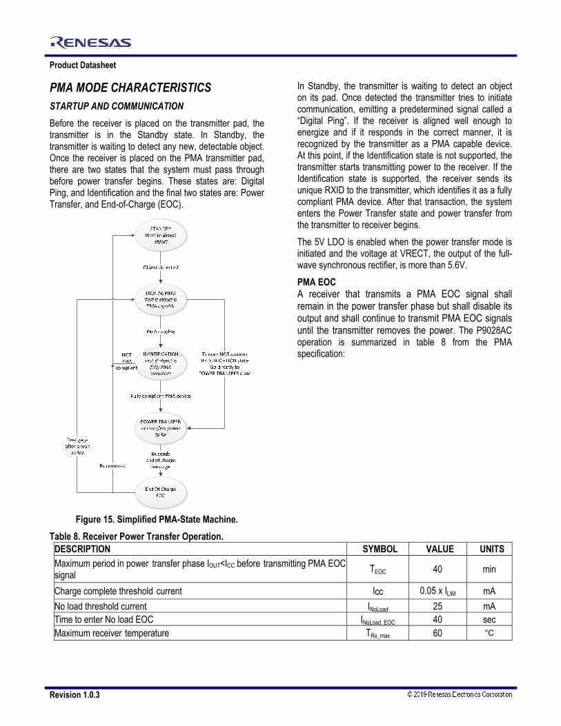
PMA MODE CHARACTERISTICS STARTUP AND COMMUNICATION
Before the receiver is placed on the transmitter pad, the transmitter is in the Standby state. In Standby, the transmitter is waiting to detect any new, detectable object. Once the receiver is placed on the PMA transmitter pad, there are two states that the system must pass through before power transfer begins. These states are: Digital Ping, and Identification and the final two states are: Power Transfer, and End-of-Charge (EOC).
Figure 15. Simplified PMA-State Machine.
Table 8. Receiver Power Transfer Operation.
In Standby, the transmitter is waiting to detect an object on its pad. Once detected the transmitter tries to initiate communication, emitting a predetermined signal called a “Digital Ping”. If the receiver is aligned well enough to energize and if it responds in the correct manner, it is recognized by the transmitter as a PMA capable device. At this point, if the Identification state is not supported, the transmitter starts transmitting power to the receiver. If the Identification state is supported, the receiver sends its unique RXID to the transmitter, which identifies it as a fully compliant PMA device. After that transaction, the system enters the Power Transfer state and power transfer from the transmitter to receiver begins.
The 5V LDO is enabled when the power transfer mode is initiated and the voltage at VRECT, the output of the full-wave synchronous rectifier, is more than 5.6V.
PMA EOC A receiver that transmits a PMA EOC signal shall remain in the power transfer phase but shall disable its output and shall continue to transmit PMA EOC signals until the transmitter removes the power. The P9028AC operation is summarized in table 8 from the PMA specification:
DESCRIPTION SYMBOL VALUE UNITS Maximum period in power transfer phase IOUT<ICC before transmitting PMA EOC signal
TEOC 40 min
Charge complete threshold current Icc 0.05 x ILIM mA
No load threshold current INoLoad 25 mA Time to enter No load EOC INoLoad_EOC 40 sec Maximum receiver temperature TRx_max 60 °C

P9028AC
Product Datasheet
Revision 1.0.3 21 © 2015 Integrated Device Technology, Inc.
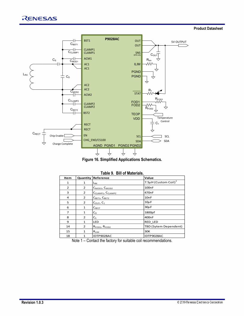
APPLICATIONS INFORMATION EXTERNAL COMPONENTS The P9028AC requires a minimum number of external components for proper operation, as indicated in Figure 16, 17 and 18 as well as Table 9, 10 and 11.
LDO Input Capacitor (VRECT Capacitors)
The LDO input capacitors (VRECT capacitors) should be located as close as possible to the VRECT pins, and ground (PGND). Ceramic capacitors are recommended for their lower ESR and small profile. See Figure 17 and Table 10 for values and type of capacitor.
VDD Capacitor
The P9028AC has an internal LDO regulator that must have a capacitor connected from the VDD pin to GND. This capacitor should be as close as possible to the VDD pin with a close GND connection. See Figure 17, 18 and Table 10, 11 for values and type of capacitor.
Output Capacitor
The output capacitor connection to the ground pin (PGND) should be made as short as practical for maximum device performance. Since the LDO has been designed to function with very low ESR capacitors, a ceramic capacitor is recommended for best performance. For better transient response increase the total amount of output capacitance. For 1A load steps, an output capacitance of at least 10µF is recommended.
PCB LAYOUT CONSIDERATIONS - For optimum device performance and lowest output
phase noise, the following guidelines should be observed. Please contact IDT Inc. for Gerber files that contain the recommended board layout and application note AN883, “P9028AC Layout Guidelines”.
- An optimum layout is one with all components on the same side of the board, minimizing vias through other signal layers. Signal traces not related to the P9028AC should be routed away from the IC as much as possible to avoid blocking thermal dissipation paths from the IC to the PCB. This includes signal traces just underneath the device, or on layers adjacent to the ground plane layer used by the device.
- Layout and PCB design have a significant influence on the power dissipation capabilities of power management ICs because the surface mount packages used with these devices rely heavily on thermally conductive traces or pads to transfer heat away from the package. Appropriate PC layout techniques should be used to remove the heat due to device power dissipation.
- The following general guidelines will be helpful in designing a board layout for lowest thermal resistance:
1. PC board traces with large cross-sectional areas remove more heat. For optimum results, use large-area PCB patterns with wide copper traces, placed on the uppermost side of the PCB.
2. In cases where maximum heat dissipation is required, use double-sided copper planes connected with multiple vias.
3. Thermal vias are needed to provide a thermal path to inner and/or bottom layers of the PCB to remove the heat generated by device power dissipation.
POWER DISSIPATION AND THERMAL REQUIREMENTS The P9028AC is offered in a QFN-32 package which has a maximum power dissipation capability of about 1.9W and in a WLCSP package, the maximum power dissipation of which is determined by the number of thermal vias between the package and the printed circuit board. The maximum power dissipation of both packages is defined by the die’s specified maximum operating junction temperature, TJ, of 125°C. The junction temperature rises when the heat generated by the device’s power dissipation goes through the package thermal resistance. The QFN package offers a typical thermal resistance, junction to ambient (ΘJA), of 35OC/W when the PCB layout and surrounding devices are optimized as described in the PCB Layout Considerations section. The WLCSP package has a typical ΘJA of 70ºC/W with 7 thermal vias and 144ºC/W with no thermal vias. Clearly, maximizing the thermal vias is highly recommended. The techniques as noted in the PCB layout section must be followed when designing the printed circuit board layout, as well as the placement of the P9028AC IC package in proximity to other heat-

P9028AC
Product Datasheet
Revision 1.0.3 22 © 2015 Integrated Device Technology, Inc.
generating devices in a given application design. The ambient temperature around the power IC will also have an effect on the thermal limits of an application. The main factors influencing ΘJA (in the order of decreasing influence) are PCB characteristics, Die/package attach thermal pad size (QFN), thermal vias (WLCSP), and internal package construction. Board designers should keep in mind that the package thermal metric ΘJA is impacted by the characteristics of the PCB itself upon which the IC is mounted. For example, in a still-air environment, as is often the case, a significant amount of the heat generated (~85%) is absorbed by the PCB. Changing the design or configuration of the PCB changes the overall thermal resistivity and, thus, the board’s heat-sinking efficiency.
The use of integrated circuits in low-profile and fine-pitch surface-mount packages requires special attention to power dissipation. Many system-dependant issues such as thermal coupling, airflow, added heat sinks and convection surfaces, and the presence of other heat-generating components, affect the power-dissipation limits of a given component.
Three basic approaches for enhancing thermal performance are listed below:
1. Improving the power dissipation capability of the PCB design
2. Improving the thermal coupling of the component to the PCB
3. Introducing airflow into the system First, the maximum power dissipation for a given situation should be calculated:
PD(MAX) = (TJ(MAX) - TA)/θJA
In which
PD(MAX) = Maximum Power Dissipation
θJA = Package Thermal Resistance (°C/W)
TJ(MAX) = Maximum Device Junction Temperature (°C)
TA = Ambient Temperature (°C)
The maximum recommended junction temperature (TJ(MAX)) for the P9028AC device is 125°C. The thermal resistance of the 32-pin QFN package (NBG32) is nominally θJA=35°C/W. Operation is specified to a maximum steady-state ambient temperature (TA) of 85°C. Therefore, the maximum recommended power dissipation is:
PD(Max) = (125°C - 85°C) / 35°C/W 1.14 Watt.
The thermal resistance for the WLCSP package (AWG36) is nominally θJA=70°C/W with 7 thermal vias, the maximum recommended power dissipation is:
PD(Max) = (125°C - 85°C) / 70°C/W 0.57 Watt
All the above-mentioned thermal resistances are the values found when the ICs are mounted on a standard board of the dimensions and characteristics specified by the JEDEC 51 standard.
THERMAL OVERLOAD PROTECTION
The P9028AC integrates thermal overload shutdown circuitry to prevent damage resulting from excessive thermal stress that may be encountered under fault conditions. This circuitry will shut down or reset the device if the die temperature exceeds 150°C. To allow the maximum load current on each regulator and the synchronous rectifier, and to prevent thermal overload, it is important to ensure that the heat generated by the P9028AC is dissipated into the PCB.
End of Charge (EOC)
In the event of thermal shutdown (150°C), EN, CHG_END or TEOP pins assertion the device turns off the LDO and continually sends End Of Power (EOP) packets in WPC or End Of Charge (EOC) in PMA until the transmitter removes the power and the rectifier voltage on the receiver side drops below the UVLO threshold.
NC pins that are indicated as “Not Internally Connected” should be soldered to the PCB ground plane to improve thermal performance with multiple vias exiting the bottom side of the PCB. This improves heat flow away from the package and minimizes package thermal gradients. DNC pins that are indicated as “Internally connected” MUST BE LEFT FLOATING. Special Notes TQFN NBG32 Package Assembly Note 1: Unopened Dry Packaged Parts have a one year shelf life. Note 2: The HIC indicator card for newly-opened Dry Packaged Parts should be checked. If there is any moisture content, the parts must be baked for a minimum of 8 hours at 125˚C within 24 hours of the assembly reflow process.
P9028AC
Product Datasheet
Revision 1.0.3 23 © 2015 Integrated Device Technology, Inc.
P9028AC
AC1
AC1
RECT
RECT
CRECT
PGND1
STATR1
AGND
AC2
AC2
SCL
SDA
SCL
SDA
CS
CD
OUT
OUT
COUT
5V OUTPUT
ACM1
ACM2
CMOD1
CMOD2
CCLAMP2
CCLAMP1
CBST1
CBST2
CLAMP2
BST2
BST1
CLAMP1
PGND
PGND
ILIM
Rlim
LRX
FOD1RFOD1
C1
VDD
CLAMP2
PGND2 PGND2
CLAMP1
FOD2RFOD2
TEOPTemperature
Control
ENChip Enable
Charge Complete
CHG_END/CS100
SNSQFN only
Figure 16. Simplified Applications Schematics.
Table 9. Bill of Materials. Item Quantity Reference Value
1 1 LRX 7.5H (Custom Coil)1
2 2 CMOD1, CMOD2 100nF
3 2 CCLAMP1, CCLAMP2 470nF
4 2 CBST1, CBST2 10nF
5 2 COUT, C1 10F
6 1 CRECT 30F
7 1 CD 1800pf
8 2 CS 400nF
9 1 LED RED_LED
14 2 RFOD1, RFOD2 TBD (Sytem Dependent)
15 1 RLIM 30K
18 1 IDTP9028AC IDTP9028AC Note 1 – Contact the factory for suitable coil recommendations.

P9028AC
Product Datasheet
Revision 1.0.3 24 © 2015 Integrated Device Technology, Inc.
DETAILED SYSTEM DIAGRAM WLCSP
Figure 17. P9028AC WLCSP Applications Schematic (See P9028AC Evaluation Kit User Manual for complete details).

P9028AC
Product Datasheet
Revision 1.0.3 25 © 2015 Integrated Device Technology, Inc.
COMPONENTS SELECTION WLCSP Table 10. P9028AC WLCSP Evaluation Kit Bill of Materials.
Item Quantity Reference Part Number Value PCB Footprint
1 1 /EN TP tp_25mil
2 2 C9,C16 C1005X7R1H103K050BB 10nF 402
3 2 C10,C15 UMK105ABJ474KV‐F 0.47uF 402
4 6 C11,C12,C27,C28,C29,C42 GRM155R61H104KE19D 0.1uF 402
5 9 C20,C21,C34,C35,C38,C39, GRM155R61E475M 4.7uF 402
C43,C44,C45
6 2 C24,C32 C1005X5R1E105M050BC 1uF 402
7 1 C26 GRM155R71H182KA01D 1.8nF 402
8 3 OUT1,GND1,VRECT 5015 1P test_pt_sm_135x70
9 2 R3,R4 TBD NP 402
10 2 R5,R6 ERJ‐1GEF3002C 30K 201
11 2 R96,R97 ERJ‐2GEJ472X 4.7K 402
12 1 U1 P9028AC IDTP9028AC CSP CSP36P500X500
Optional Components
13 4 CS100,TEOP,STAT,INT TP tp_25mil
14 8 AC2,GND3,GND4,GND5,GND6, 28AWG 28AWG
AC11,SDA,SCL
15 1 C41 GRM155R61E475M NP 402
16 4 GND,FOD1,GND2,FOD2, 5015 1P test_pt_sm_135x70
17 1 J1 SBH11‐PBPC‐D07‐ST‐BK 14P P_014_2R
18 2 R1,R2 3223W‐1‐504E 500K res_adj_smd_3p9x3p9
19 1 R82 ERJ‐2GE0R00X 0 402
20 1 R85 RC0402JR‐070RL 0 402
P9028AC
Product Datasheet
Revision 1.0.3 26 © 2015 Integrated Device Technology, Inc.
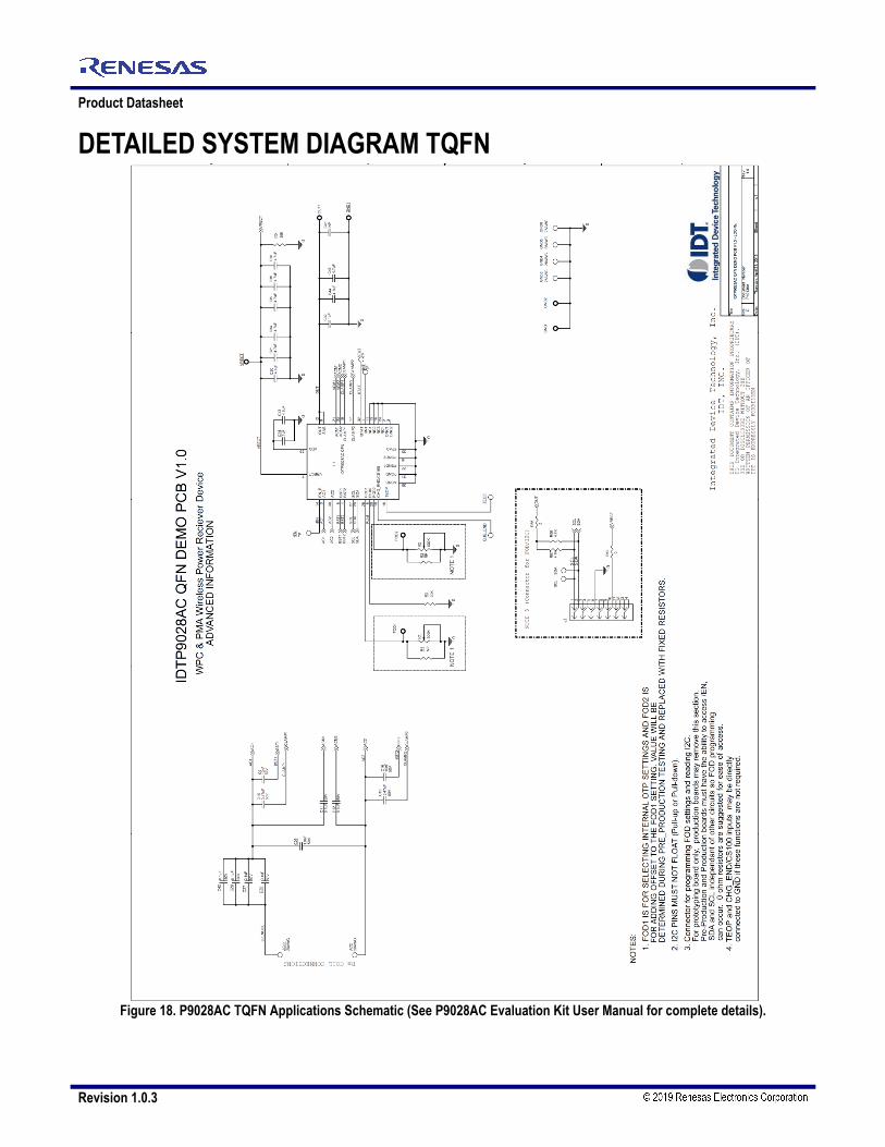
DETAILED SYSTEM DIAGRAM TQFN
Figure 18. P9028AC TQFN Applications Schematic (See P9028AC Evaluation Kit User Manual for complete details).
P9028AC
Product Datasheet
Revision 1.0.3 27 © 2015 Integrated Device Technology, Inc.
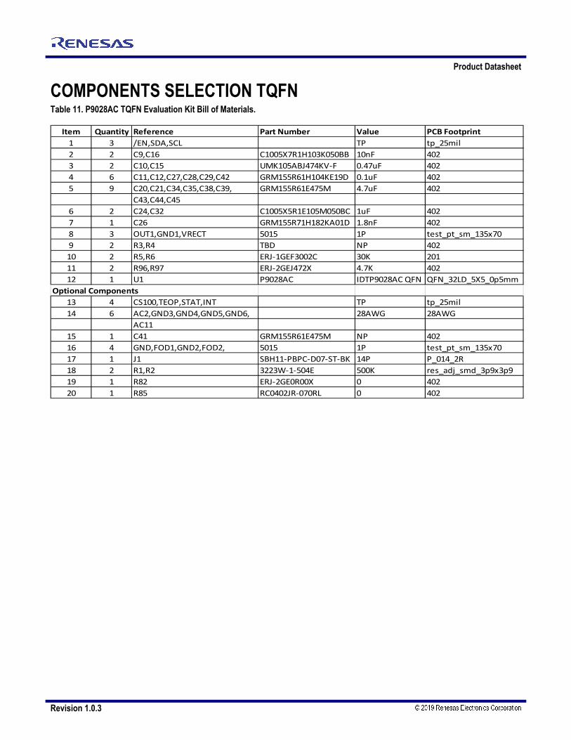
COMPONENTS SELECTION TQFN Table 11. P9028AC TQFN Evaluation Kit Bill of Materials.
Item Quantity Reference Part Number Value PCB Footprint
1 3 /EN,SDA,SCL TP tp_25mil
2 2 C9,C16 C1005X7R1H103K050BB 10nF 402
3 2 C10,C15 UMK105ABJ474KV‐F 0.47uF 402
4 6 C11,C12,C27,C28,C29,C42 GRM155R61H104KE19D 0.1uF 402
5 9 C20,C21,C34,C35,C38,C39, GRM155R61E475M 4.7uF 402
C43,C44,C45
6 2 C24,C32 C1005X5R1E105M050BC 1uF 402
7 1 C26 GRM155R71H182KA01D 1.8nF 402
8 3 OUT1,GND1,VRECT 5015 1P test_pt_sm_135x70
9 2 R3,R4 TBD NP 402
10 2 R5,R6 ERJ‐1GEF3002C 30K 201
11 2 R96,R97 ERJ‐2GEJ472X 4.7K 402
12 1 U1 P9028AC IDTP9028AC QFN QFN_32LD_5X5_0p5mm
Optional Components
13 4 CS100,TEOP,STAT,INT TP tp_25mil
14 6 AC2,GND3,GND4,GND5,GND6, 28AWG 28AWG
AC11
15 1 C41 GRM155R61E475M NP 402
16 4 GND,FOD1,GND2,FOD2, 5015 1P test_pt_sm_135x70
17 1 J1 SBH11‐PBPC‐D07‐ST‐BK 14P P_014_2R
18 2 R1,R2 3223W‐1‐504E 500K res_adj_smd_3p9x3p9
19 1 R82 ERJ‐2GE0R00X 0 402
20 1 R85 RC0402JR‐070RL 0 402

P9028AC
Product Datasheet
Revision 1.0.3 28 © 2015 Integrated Device Technology, Inc.
I2C REGISTER MAP The P9028AC has a one-time programmable I2C address that is set to default 0X25h. Table 12. READ Registers - VRECT voltage: VRECT=5 X ADC1<12:1> = [ADC1<12:1>] X 5 X [1.8V/212].
Byte
Address
Byte
Name Bit Field Field Name Type
Default
Value Description
0x40 REG0 7 ADC1<12> R VRECT ADC code (average of 8 consecutive measurements) 0x40 REG0 6 ADC1<11> R VRECT ADC code (average of 8 consecutive measurements) 0x40 REG0 5 ADC1<10> R VRECT ADC code (average of 8 consecutive measurements) 0x40 REG0 4 ADC1<9> R VRECT ADC code (average of 8 consecutive measurements) 0x40 REG0 3 ADC1<8> R VRECT ADC code (average of 8 consecutive measurements) 0x40 REG0 2 ADC1<7> R VRECT ADC code (average of 8 consecutive measurements) 0x40 REG0 1 ADC1<6> R VRECT ADC code (average of 8 consecutive measurements) 0x40 REG0 0 ADC1<5> R VRECT ADC code (average of 8 consecutive measurements) 0x41 REG1 7 ADC1<4> R VRECT ADC code (average of 8 consecutive measurements) 0x41 REG1 6 ADC1<3> R VRECT ADC code (average of 8 consecutive measurements) 0x41 REG1 5 ADC1<2> R VRECT ADC code (average of 8 consecutive measurements) 0x41 REG1 4 ADC1<1> R VRECT ADC code (average of 8 consecutive measurements) 0x41 REG1 3 RESERVED. R RESERVED. 0x41 REG1 2 RESERVED. R RESERVED. 0x41 REG1 1 RESERVED. R RESERVED. 0x41 REG1 0 RESERVED. R RESERVED.

P9028AC
Product Datasheet
Revision 1.0.3 29 © 2015 Integrated Device Technology, Inc.
I2C REGISTER MAP (CONTINUED) Table 13. READ Registers - Iout current: IOUT is read directly from IOUT = ADC2<12:1> = [ADC1<12:1>] X [1.8A/212].
Byte
Address
Byte
Name Bit Field Field Name Type
Default
Value Description
0x42 REG2 7 ADC2<12> R Iout ADC code (average of 8 consecutive measurements)
0x42 REG2 6 ADC2<11> R Iout ADC code (average of 8 consecutive measurements)
0x42 REG2 5 ADC2<10> R Iout ADC code (average of 8 consecutive measurements)
0x42 REG2 4 ADC2<9> R Iout ADC code (average of 8 consecutive measurements)
0x42 REG2 3 ADC2<8> R Iout ADC code (average of 8 consecutive measurements)
0x42 REG2 2 ADC2<7> R Iout ADC code (average of 8 consecutive measurements)
0x42 REG2 1 ADC2<6> R Iout ADC code (average of 8 consecutive measurements)
0x42 REG2 0 ADC2<5> R Iout ADC code (average of 8 consecutive measurements)
0X43 REG3 7 ADC2<4> R Iout ADC code (average of 8 consecutive measurements)
0X43 REG3 6 ADC2<3> R Iout ADC code (average of 8 consecutive measurements)
0X43 REG3 5 ADC2<2> R Iout ADC code (average of 8 consecutive measurements)
0X43 REG3 4 ADC2<1> R Iout ADC code (average of 8 consecutive measurements)
0X43 REG3 3 RESERVED. R RESERVED.
0X43 REG3 2 RESERVED. R RESERVED.
0X43 REG3 1 RESERVED. R RESERVED.
0x43 REG3 0 RESERVED. R RESERVED.

P9028AC
Product Datasheet
Revision 1.0.3 30 © 2015 Integrated Device Technology, Inc.
I2C REGISTER MAP (CONTINUED)
Table 14. READ Registers - Frequency: , where COUNT is the decimal number represented by
FREQ<10:1>. Byte
Address
Byte
Name Bit Field Field Name Type
Default
Value Description
0X44 REG4 7 FREQ<10> R Frequency value (10 bits).
0X44 REG4 6 FREQ<9> R Frequency value (10 bits).
0X44 REG4 5 FREQ<8> R Frequency value (10 bits).
0X44 REG4 4 FREQ<7> R Frequency value (10 bits).
0X44 REG4 3 FREQ<6> R Frequency value (10 bits).
0X44 REG4 2 FREQ<5> R Frequency value (10 bits).
0X44 REG4 1 FREQ<4> R Frequency value (10 bits).
0X44 REG4 0 FREQ<3> R Frequency value (10 bits).
0X45 REG5 7 FREQ<2> R Frequency value (10 bits).
0X45 REG5 6 FREQ<1> R Frequency value (10 bits).
0X45 REG5 5 RESERVED. R RESERVED.
0X45 REG5 4 RESERVED. R RESERVED.
0X45 REG5 3 RESERVED. R RESERVED.
0X45 REG5 2 RESERVED. R RESERVED.
0X45 REG5 1 RESERVED. R RESERVED.
0X45 REG5 0 RESERVED. R RESERVED.

P9028AC
Product Datasheet
Revision 1.0.3 31 © 2015 Integrated Device Technology, Inc.
I2C REGISTER MAP (CONTINUED) Table 15. READ Registers – Miscellaneous functions.
Byte
Address
Byte
Name Bit Field Field Name Type
Default
Value Description
0X47 REG7 3 UVLO R 1: VRECT is higher than UVLO threshold 0 : No meaning.
0X47 REG7 2 CLAMP_ON R 0: VRECT is lower than AC clamp threshold 1 : VRECT is higher than AC clamp threshold
0X47 REG7 1 LDO_CL R 0: Normal Operation 1: LDO current limit exceeded.
0X47 REG7 0 RESERVED. R RESERVED.
0X48 REG8 7 CHARGE_COMPLETE R 0: No meaning. 1: Charge Complete..
0X48 REG8 6 RESERVED. R RESERVED.
0X48 REG8 5 RESERVED. R RESERVED.
0X48 REG8 4 RESERVED. R RESERVED.
0X48 REG8 3 RESERVED. R RESERVED.
0X48 REG8 2 RESERVED. R RESERVED.
0X48 REG8 1 DIE_TEMP R 0: Die Temperature < 150C 1: Die Temperature >150C
0x48 REG8 0 TX_TYPE R 0: TX is WPC 1: TX is PMA
0x54 REG20 [7:0] WPC_ID_B0 R Read OTP26 content.
0x55 REG21 [7:0] WPC_ID_B1 R Read OTP27 content.
0x56 REG22 [7:0] WPC_ID_B2 R Read OTP28 content.
0x57 REG23 [7:0] WPC_ID_B3 R Read OTP29 content.
0x58 REG24 [7:0] WPC_ID_B4 R Read OTP30 content.
0x59 REG25 [7:0] WPC_ID_B5 R Read OTP31 content.
0x5A REG26 [7:0] WPC_ID_B6 R Read OTP32 content.
0x5B REG27 [7:0] PMA_RXID_PRE R Read OTP33 content.
0x5C REG28 [7:0] PMA_RXID_MSG R Read OTP34 content.
0x5D REG29 [7:0] PMA_RXID_CER R Read OTP35 content.
0x5E REG30 [7:0] PMA_RXID_B0 R Read OTP36 content.
0x5F REG31 [7:0] PMA_RXID_B1 R Read OTP37 content.
0x60 REG32 [7:0] PMA_RXID_B2 R Read OTP38 content.
0x61 REG33 [7:0] PMA_RXID_B3 R Read OTP39 content.
0x62 REG34 [7:0] PMA_RXID_B4 R Read OTP40 content.
0x63 REG35 [7:0] PMA_RXID_B5 R Read OTP41 content.
0x64 REG36 [7:0] PMA_RXID_CRCB0 R Read OTP42 content.
0x65 REG37 [7:0] PMA_RXID_CRCB1 R Read OTP43 content.

P9028AC
Product Datasheet
Revision 1.0.3 32 © 2015 Integrated Device Technology, Inc.
I2C REGISTER MAP (CONTINUED) Table 16. Read-Write physical FOD registers: See Application Note #814A.
Byte
Address
Byte
Name
Bit
Field Field Name Type
Default
Value Description
0X49 REG9 0-7 FOD9<0-7> R/W 0 mcf correction for Region 1 IO1,IO2,IO3=000
0X4A REG10 0-7 FOD10<0-7> R/W 0 bcf correction for Region 1 IO1,IO2,IO3=000
0X4B REG11 0-7 FOD11<0-7> R/W 0 mcf correction for Region 2 IO1,IO2,IO3=010
0X4C REG12 0-7 FOD12<0-7> R/W 0 bcf correction for Region 2 IO1,IO2,IO3=010
0X4D REG13 0-7 FOD13<0-7> R/W 0 mcf correction for Region 3 IO1,IO2,IO3=100
0X4E REG14 0-7 FOD14<0-7> R/W 0 bcf correction for Region 3 IO1,IO2,IO3=100
0X4F REG15 0-7 FOD15<0-7> R/W 0 mcf correction for Region 4 IO1,IO2,IO3=110
0X50 REG16 0-7 FOD16<0-7> R/W 0 bcf correction for Region 4 IO1,IO2,IO3=110
0X51 REG17 0-7 FOD17<0-7> R/W 0 mcf correction for Region 5 IO1,IO2,IO3=111
0X52 REG18 0-7 FOD18<0-7> R/W 0 bcf correction for Region 5 IO1,IO2,IO3=111
0X53 REG19 0-7 FOD19<0-7> R/W 0 bcf correction for start-up phase

P9028AC
Product Datasheet
Revision 1.0.3 33 © 2015 Integrated Device Technology, Inc.
PACKAGE OUTLINE DRAWING WLCSP
Figure 19. WLCSP Package Outline Drawing (AWG36).
P9028AC
Product Datasheet
Revision 1.0.3 34 © 2015 Integrated Device Technology, Inc.
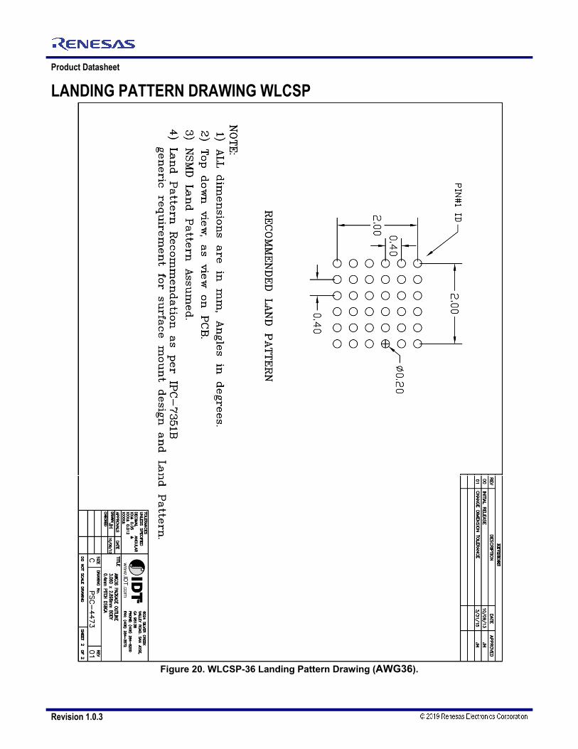
LANDING PATTERN DRAWING WLCSP
Figure 20. WLCSP-36 Landing Pattern Drawing (AWG36).

P9028AC
Product Datasheet
Revision 1.0.3 35 © 2015 Integrated Device Technology, Inc.
PACKAGE OUTLINE DRAWING TQFN
Figure 21. TQFN Package Outline Drawing (NBG32).

P9028AC
Product Datasheet
Revision 1.0.3 36 © 2015 Integrated Device Technology, Inc.
LANDING PATTERN DRAWING TQFN
Figure 22. QFN-40 5mmx5mm Landing Pattern Drawing (NBG32).

P9028AC
Product Datasheet
Revision 1.0.3 37 © 2015 Integrated Device Technology, Inc.
REVISION HISTORY Revision Changes
1.0.0 Initial release
1.0.1 Page 23: Corrected TEOP pin name.
Page 41: Removed TS pin register descriptions.
1.0.2 Page 3: Added Note: For the WLCSP (AWG36) package, connecting the 7 thermal balls to internal/external ground planes from top to bottom sides of the PCB, is recommended for improving the overall thermal performance.
Page 23: Corrected part number P9028AC
Page 29: Added information to the sentence. The thermal resistance for the WLCSP package (AWG36) is nominally θJA=70°C/W with 7 thermal vias, the maximum recommended power dissipation is:
1.0.3 Pages 24, 25, 26, 27: Added 30k (R6) resistor from VRECT pin to ground to schematic and BOM. Resistor is needed to pass PMA3 certification, ping detection test. Added TQFN schematic and BOM.

P9028AC Product Datasheet
Revision 1.0.3 38
Ordering Guide Table 17. Ordering Summary.
IDT PART NUMBER
PART NUMBER MARKING PACKAGE AMBIENT TEMP. RANGE
SHIPPING CARRIER
P9028AC-x* P9028AC- xAWGI8 P9028AC- xAWGI WLCSP 36 0°C to +85°C Tape and Reel P9028AC-x* P9028AC-x*NBGI P9028AC-x*NBGI TQFN 32 0°C to +85°C Tray P9028AC-x* P9028AC-x*NBGI8 P9028AC-x*NBGI8 TQFN 32 0°C to +85°C Tape and Reel
*Note – this field is a custom value that is specific to each customer. Please contact your local sales team for your particularvalue for this field.

Corporate HeadquartersTOYOSU FORESIA, 3-2-24 Toyosu,Koto-ku, Tokyo 135-0061, Japanwww.renesas.com
Contact InformationFor further information on a product, technology, the most up-to-date version of a document, or your nearest sales office, please visit:www.renesas.com/contact/
TrademarksRenesas and the Renesas logo are trademarks of Renesas Electronics Corporation. All trademarks and registered trademarks are the property of their respective owners.
IMPORTANT NOTICE AND DISCLAIMER
RENESAS ELECTRONICS CORPORATION AND ITS SUBSIDIARIES (“RENESAS”) PROVIDES TECHNICAL SPECIFICATIONS AND RELIABILITY DATA (INCLUDING DATASHEETS), DESIGN RESOURCES (INCLUDING REFERENCE DESIGNS), APPLICATION OR OTHER DESIGN ADVICE, WEB TOOLS, SAFETY INFORMATION, AND OTHER RESOURCES “AS IS” AND WITH ALL FAULTS, AND DISCLAIMS ALL WARRANTIES, EXPRESS OR IMPLIED, INCLUDING, WITHOUT LIMITATION, ANY IMPLIED WARRANTIES OF MERCHANTABILITY, FITNESS FOR A PARTICULAR PURPOSE, OR NON-INFRINGEMENT OF THIRD PARTY INTELLECTUAL PROPERTY RIGHTS.
These resources are intended for developers skilled in the art designing with Renesas products. You are solely responsible for (1) selecting the appropriate products for your application, (2) designing, validating, and testing your application, and (3) ensuring your application meets applicable standards, and any other safety, security, or other requirements. These resources are subject to change without notice. Renesas grants you permission to use these resources only for development of an application that uses Renesas products. Other reproduction or use of these resources is strictly prohibited. No license is granted to any other Renesas intellectual property or to any third party intellectual property. Renesas disclaims responsibility for, and you will fully indemnify Renesas and its representatives against, any claims, damages, costs, losses, or liabilities arising out of your use of these resources. Renesas' products are provided only subject to Renesas' Terms and Conditions of Sale or other applicable terms agreed to in writing. No use of any Renesas resources expands or otherwise alters any applicable warranties or warranty disclaimers for these products.
(Rev.1.0 Mar 2020)
© 2020 Renesas Electronics Corporation. All rights reserved.