Download - with ABZ Incremental & PWM Outputs

MagAlpha MA730 14-Bit, Digital, Contactless Angle Sensor
with ABZ Incremental & PWM Outputs
MA730 Rev. 1.01 www.MonolithicPower.com 1 10/13/2017 MPS Proprietary Information. Patent Protected. Unauthorized Photocopy and Duplication Prohibited. © 2017 MPS. All Rights Reserved.
DESCRIPTION The MA730 detects the absolute angular position of a permanent magnet, typically a diametrically magnetized cylinder on a rotating shaft. Fast data acquisition and processing provide accurate angle measurements at speeds from 0 to 60,000 rpm.
The MA730 supports a wide range of magnetic field strengths and spatial configurations. Both end-of-shaft and off-axis (side-shaft mounting) configurations are supported.
The MA730 features magnetic field strength detection with programmable thresholds to allow sensing of the magnet position relative to the sensor for creation of functions, such as the sensing of axial movements or for diagnostics.
On-chip non-volatile memory provides storage for configuration parameters, including the reference zero angle position, ABZ encoder settings, and magnetic field detection thresholds.
FEATURES
14-Bit Resolution Absolute Angle Encoder
Contactless Sensing for Long Life
SPI Serial Interface for Digital Angle Readout and Chip Configuration
Incremental 12-Bit ABZ Quadrature Encoder Interface with Programmable Pulses Per Turn from 1 - 1024
PWM Output 14-Bit
Programmable Magnetic Field Strength Detection for Diagnostic Checks
3.3V, 12mA Supply
-40°C to +125°C Operating Temperature
Available in a QFN-16 (3mmx3mm) Package
APPLICATIONS
General Purpose Angle Measurements
High-Resolution Angle Encoders
Automotive Angle
Robotics
All MPS parts are lead-free, halogen-free, and adhere to the RoHS directive. For MPS green status, please visit the MPS website under Quality Assurance. “MPS” and “The Future of Analog IC Technology” are registered trademarks of Monolithic Power Systems, Inc.
TYPICAL APPLICATION

MA730 – 14-BIT, DIGITAL ANGLE SENSOR WITH ABZ & PWM OUTPUTS
MA730 Rev. 1.01 www.MonolithicPower.com 2 10/13/2017 MPS Proprietary Information. Patent Protected. Unauthorized Photocopy and Duplication Prohibited. © 2017 MPS. All Rights Reserved.
ORDERING INFORMATION
Part Number* Package Top Marking
MA730GQ QFN-16 (3mmx3mm) See Below
* For Tape & Reel, add suffix –Z (e.g. MA730GQ–Z)
TOP MARKING
AZA: Product code of MA730GQ Y: Year code LLL: Lot number
PACKAGE REFERENCE
TOP VIEW
A
Z
MOSI
CSBMISOGND
MGL
SCLK
VDD N/C MGH
SSD
PWM
SSCK
TEST
1
16
2
3
4
5678
9
12
11
10
13 14 15
17
PAD
QFN-16 (3mmx3mm)

MA730 – 14-BIT, DIGITAL ANGLE SENSOR WITH ABZ & PWM OUTPUTS
MA730 Rev. 1.01 www.MonolithicPower.com 3 10/13/2017 MPS Proprietary Information. Patent Protected. Unauthorized Photocopy and Duplication Prohibited. © 2017 MPS. All Rights Reserved.
ABSOLUTE MAXIMUM RATINGS (1) Supply voltage ............................. -0.5V to +4.6V Input pin voltage (VI) .................... -0.5V to +6.0V Output pin voltage (VO) ................ -0.5V to +4.6V
Continuous power dissipation (TA = +25°C) (2)
................................................................... 2.0W Junction temperature ................................ 125°C Lead temperature ..................................... 260°C Storage temperature .................. -65°C to 150°C
Thermal Resistance (3)
θJA θJC QFN-16 (3mmx3mm) ............. 50 ....... 12 ... °C/W
NOTES: 1) Exceeding these ratings may damage the device. 2) The maximum allowable power dissipation is a function of the
maximum junction temperature TJ (MAX), the junction-to-ambient thermal resistance θJA, and the ambient temperature TA. The maximum allowable continuous power dissipation at any ambient temperature is calculated by PD (MAX) = (TJ
(MAX)-TA)/θJA. 3) Measured on JESD51-7, 4-layer PCB.

MA730 – 14-BIT, DIGITAL ANGLE SENSOR WITH ABZ & PWM OUTPUTS
MA730 Rev. 1.01 www.MonolithicPower.com 4 10/13/2017 MPS Proprietary Information. Patent Protected. Unauthorized Photocopy and Duplication Prohibited. © 2017 MPS. All Rights Reserved.
ELECTRICAL CHARACTERISTICS
Parameter Symbol Condition Min Typ Max Units
Recommended Operating Conditions
Supply voltage VDD 3.0 3.3 3.6 V
Supply current IDD From -40°C to +125°C 10.2 11.7 13.8 mA
Operating temperature Top -40 125 °C
Applied magnetic field B 40 60 mT

MA730 – 14-BIT, DIGITAL ANGLE SENSOR WITH ABZ & PWM OUTPUTS
MA730 Rev. 1.01 www.MonolithicPower.com 5 10/13/2017 MPS Proprietary Information. Patent Protected. Unauthorized Photocopy and Duplication Prohibited. © 2017 MPS. All Rights Reserved.
GENERAL CHARACTERISTICS VDD = 3.3V, 45mT < B < 100mT, temp = -40°C to +125°C, unless otherwise noted.
Parameter Symbol Condition Min Typ Max Units
Absolute Output – Serial
Effective resolution 3σ deviation of the noise distribution 13.0 13.8 14.5 bit
Noise RMS 0.003 0.004 0.007 deg
Refresh rate 850 980 1100 kHz
Data output length 16 16 bit
Response Time
Power-up time (4)
260 ms
Latency (4)
Constant speed propagation delay 8 10 µs
Filter cutoff frequency (4)
Fcutoff 23 Hz
Accuracy
INL at 25°C At room temperature over the full field range
0.7 deg
INL between -40°C to +125°C
(5)
Over the full temperature range and field range
1.1 deg
Output Drift
Temperature induced drift at room temperature
(5)
0.015 0.04 deg/°C
Temperature induced variation
(5)
From 25°C to 85°C 0.5 1.2 deg
From 25°C to 125°C 1.0 2.1 deg
Magnetic field induced (5)
0.005 deg/mT
Voltage supply induced (5)
0.3 deg/V
Absolute Output – PWM
PWM frequency Fpwm 840 970 1090 Hz
PWM resolution 13 13.8 14.0 bit
Incremental Output – ABZ
ABZ update rate 16 MHz
Resolution - edges per turn
Programmable 4 4096
Pulses per channel per turn
PPT+1 Programmable 1 1024
ABZ hysteresis (5)
H 0.1 deg
Systematic jitter (5)
For PPT = 1023, between 0 and 100krpm, up to 60mT
11 %
For PPT = 127, between 0 and 100krpm
7 %
Random jitter (3σ)
For PPT = 255, between 0 and 100krpm
4.2 %
For PPT = 127, between 0 and 100krpm
0.5 %
Overall ABZ jitter (5)
Up to 60mT 0.2 deg

MA730 – 14-BIT, DIGITAL ANGLE SENSOR WITH ABZ & PWM OUTPUTS
MA730 Rev. 1.01 www.MonolithicPower.com 6 10/13/2017 MPS Proprietary Information. Patent Protected. Unauthorized Photocopy and Duplication Prohibited. © 2017 MPS. All Rights Reserved.
GENERAL CHARACTERISTICS (continued) VDD = 3.3V, 45mT < B < 100mT, temp = -40°C to +125°C, unless otherwise noted.
Parameter Symbol Condition Min Typ Max Units
Magnetic Field Detection Thresholds
Accuracy (5)
5 mT
Hysteresis (5)
MagHys 6 mT
Temperature drift (5)
-600 ppm/°C
Digital I/O
Input high voltage VIH 2.5 5.5 V
Input low voltage VIL -0.3 0.8 V
Output low voltage (5)
VOL IOL = 4mA 0.4 V
Output high voltage (5)
VOH IOH = 4mA 2.4 V
Pull-down resistor RPD 43 55 97 kΩ
Rising edge slew rate (4)
TR CL = 50pF 0.7 V/ns
Falling edge slew rate (4)
TF CL = 50pF 0.7 V/ns
NOTES: 4) Guaranteed by design. 5) Guaranteed by characteristic test.
MA730 – 14-BIT, DIGITAL ANGLE SENSOR WITH ABZ & PWM OUTPUTS
MA730 Rev. 1.01 www.MonolithicPower.com 7 10/13/2017 MPS Proprietary Information. Patent Protected. Unauthorized Photocopy and Duplication Prohibited. © 2017 MPS. All Rights Reserved.
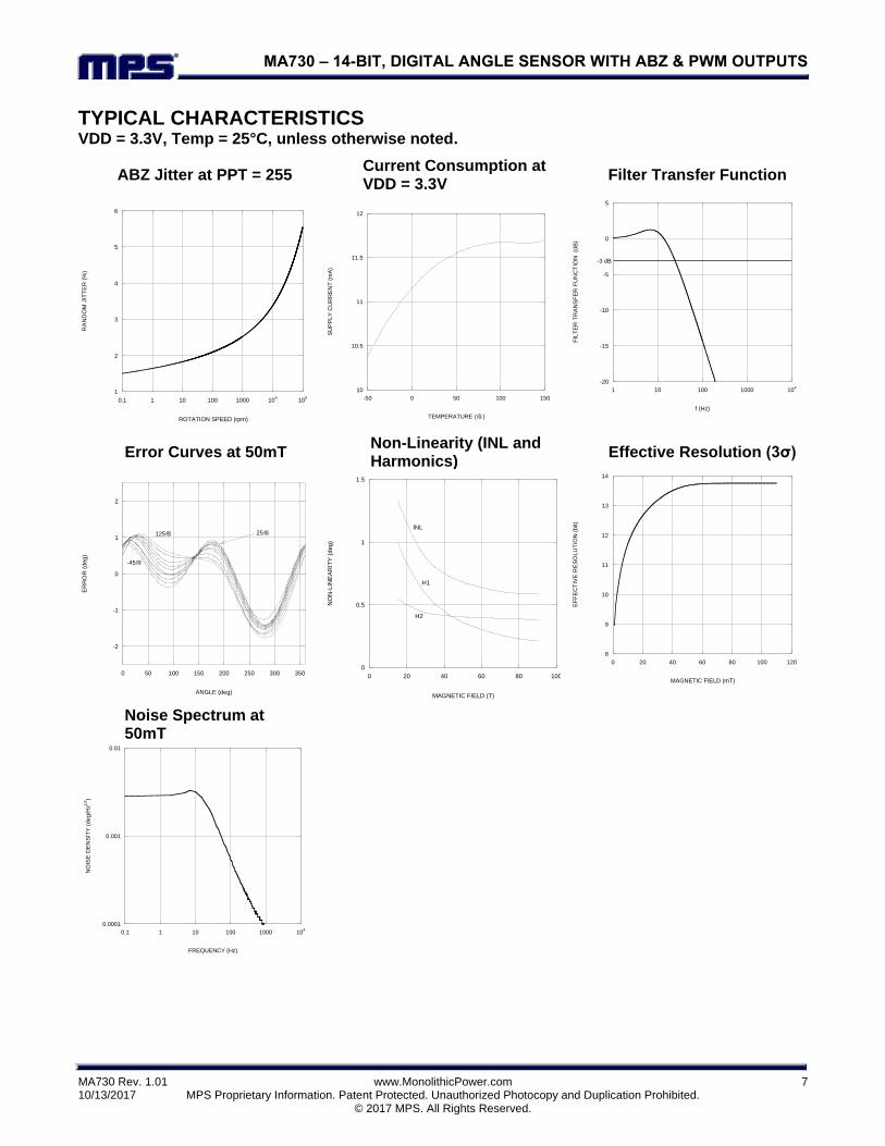
TYPICAL CHARACTERISTICS VDD = 3.3V, Temp = 25°C, unless otherwise noted.
ABZ Jitter at PPT = 255 Current Consumption at VDD = 3.3V
Filter Transfer Function
1
2
3
4
5
6
0.1 1 10 100 1000 104
105
RA
ND
OM
JIT
TE
R (
%)
ROTATION SPEED (rpm)
10
10.5
11
11.5
12
-50 0 50 100 150
SU
PP
LY
CU
RR
EN
T (
mA
)
TEMPERATURE (癈 )
-20
-15
-10
-5
0
5
1 10 100 1000 104
FIL
TE
R T
RA
NS
FE
R F
UN
CT
ION
(d
B)
f (Hz)
-3 dB
Error Curves at 50mT Non-Linearity (INL and Harmonics)
Effective Resolution (3σ)
-2
-1
0
1
2
0 50 100 150 200 250 300 350
ER
RO
R (
deg
)
ANGLE (deg)
125癈
-45癈
25癈
0
0.5
1
1.5
0 20 40 60 80 100
NO
N-L
INE
AR
ITY
(d
eg
)
MAGNETIC FIELD (T)
INL
H1
H2
8
9
10
11
12
13
14
0 20 40 60 80 100 120
EF
FE
CT
IVE
RE
SO
LU
TIO
N (
bit)
MAGNETIC FIELD (mT)
Noise Spectrum at 50mT
0.0001
0.001
0.01
0.1 1 10 100 1000 104
NO
ISE
DE
NS
ITY
(d
eg
/Hz1
/2)
FREQUENCY (Hz)

MA730 – 14-BIT, DIGITAL ANGLE SENSOR WITH ABZ & PWM OUTPUTS
MA730 Rev. 1.01 www.MonolithicPower.com 8 10/13/2017 MPS Proprietary Information. Patent Protected. Unauthorized Photocopy and Duplication Prohibited. © 2017 MPS. All Rights Reserved.
PIN FUNCTIONS
Package Pin #
Name Description
1 SSD Data out (SSI).
2 A Incremental output.
3 Z Incremental output.
4 MOSI Data in (SPI). MOSI has an internal pull-down resistor.
5 CS Chip select (SPI). CS has an internal pull-up resistor.
6 B Incremental output.
7 MISO Data out (SPI). MISO has an internal pull-down resistor that is enabled at a high impedance state.
8 GND Supply ground.
9 PWM PWM output.
10 TEST Factory use only. Connect TEST to ground.
11 MGL Digital output indicating field strength below MGLT level.
12 SCLK Clock (SPI). Internal pull-down.
13 VDD 3.3V supply.
14 NC No connection. Leave NC unconnected.
15 SSCK Clock (SSI). Internal pull-down.
16 MGH Digital output indicating field strength above MGHT level.

MA730 – 14-BIT, DIGITAL ANGLE SENSOR WITH ABZ & PWM OUTPUTS
MA730 Rev. 1.01 www.MonolithicPower.com 9 10/13/2017 MPS Proprietary Information. Patent Protected. Unauthorized Photocopy and Duplication Prohibited. © 2017 MPS. All Rights Reserved.
BLOCK DIAGRAM
Figure 1: Functional Block Diagram
MA730 – 14-BIT, DIGITAL ANGLE SENSOR WITH ABZ & UVW OUTPUTS
MA730 Rev. 1.01 www.MonolithicPower.com 10 10/13/2017 MPS Proprietary Information. Patent Protected. Unauthorized Photocopy and Duplication Prohibited. © 2017 MPS. All Rights Reserved.
OPERATION Sensor Front-End
The magnetic field is detected with integrated Hall devices located in the center of the package. The angle is measured using the SpinaxisTM method, which digitizes the direction of the field directly without complex arctangent computations or feedback loop-based circuits (interpolators).
The SpinaxisTM method is based on phase detection and generates a sinusoidal signal with a phase that represents the angle of the magnetic field. The angle is then obtained by a time-to-digital converter, which measures the time between the zero crossing of the sinusoidal signal and the edge of a constant waveform (see Figure 2). The time-to-digital is output from the front-end to the digital conditioning block.
Top: Sine Waveform Bottom: Clock of Time-to-Digital Converter
Figure 2: Phase Detection Method
The output of the front-end delivers a digital number proportional to the angle of the magnetic field at the rate of 1MHz in a straightforward and open-loop manner.
Digital Filtering
The front-end signal is further treated to achieve the final effective resolution. This treatment does not add any latency in steady conditions. The filter transfer function can be calculated with Equation (1):
2
1 2 sH(s)
(1 s)
(1)
Where τ is the filter time constant related to the cutoff frequency by τ = 0.38/Fcutoff. See the General Characteristics table on page 5 for the value of Fcutoff.
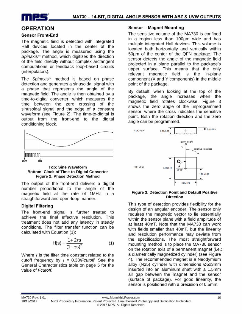
Sensor – Magnet Mounting
The sensitive volume of the MA730 is confined in a region less than 100µm wide and has multiple integrated Hall devices. This volume is located both horizontally and vertically within 50µm of the center of the QFN package. The sensor detects the angle of the magnetic field projected in a plane parallel to the package’s upper surface. This means that the only relevant magnetic field is the in-plane component (X and Y components) in the middle point of the package.
By default, when looking at the top of the package, the angle increases when the magnetic field rotates clockwise. Figure 3 shows the zero angle of the unprogrammed sensor, where the cross indicates the sensitive point. Both the rotation direction and the zero angle can be programmed.
Figure 3: Detection Point and Default Positive Direction
This type of detection provides flexibility for the design of an angular encoder. The sensor only requires the magnetic vector to lie essentially within the sensor plane with a field amplitude of at least 40mT. Note that the MA730 can work with fields smaller than 40mT, but the linearity and resolution performance may deviate from the specifications. The most straightforward mounting method is to place the MA730 sensor on the rotation axis of a permanent magnet (i.e.: a diametrically magnetized cylinder) (see Figure 4). The recommended magnet is a Neodymium alloy (N35) cylinder with dimensions Ø5x3mm inserted into an aluminum shaft with a 1.5mm air gap between the magnet and the sensor (surface of package). For good linearity, the sensor is positioned with a precision of 0.5mm.

MA730 – 14-BIT, DIGITAL ANGLE SENSOR WITH ABZ & UVW OUTPUTS
MA730 Rev. 1.01 www.MonolithicPower.com 11 10/13/2017 MPS Proprietary Information. Patent Protected. Unauthorized Photocopy and Duplication Prohibited. © 2017 MPS. All Rights Reserved.
Figure 4: End-of-Shaft Mounting
If the end-of-shaft position is not available, the sensor can be positioned away from the rotation axis of a cylinder or ring magnet (see Figure 5). In this case, the magnetic field angle is no longer directly proportional to the mechanical angle. The MA730 can be adjusted to compensate for this effect and recover the linear relation between the mechanical angle and the sensor output. With multiple pole pair magnets, the MA730 indicates multiple rotations for each mechanical turn.
Figure 5: Side-Shaft Mounting
Electrical Mounting and Power Supply Decoupling
It is recommended to place a 1µF decoupling capacitor close to the sensor with a low impedance path to GND (see Figure 6).
Exposed pad
MOSI
MISO
CS
SCLK
MA730
1 mF
3.3 V
SSD
SSCK
MGL MGH A B Z
PWM
GND
VDD
TEST
Figure 6: Connection for Supply Decoupling
In general, the MagAlpha works well with or without the exposed pad connected to anything. For optimal conditions (electrically, thermally, and mechanically), it is recommended that the exposed pad be connected to ground.
Serial Interface
The sensor supports the SPI serial interface for angle reading and register programming. Alternatively, the SSI bus can be used for angle reading (programming through SSI is not supported).
SPI
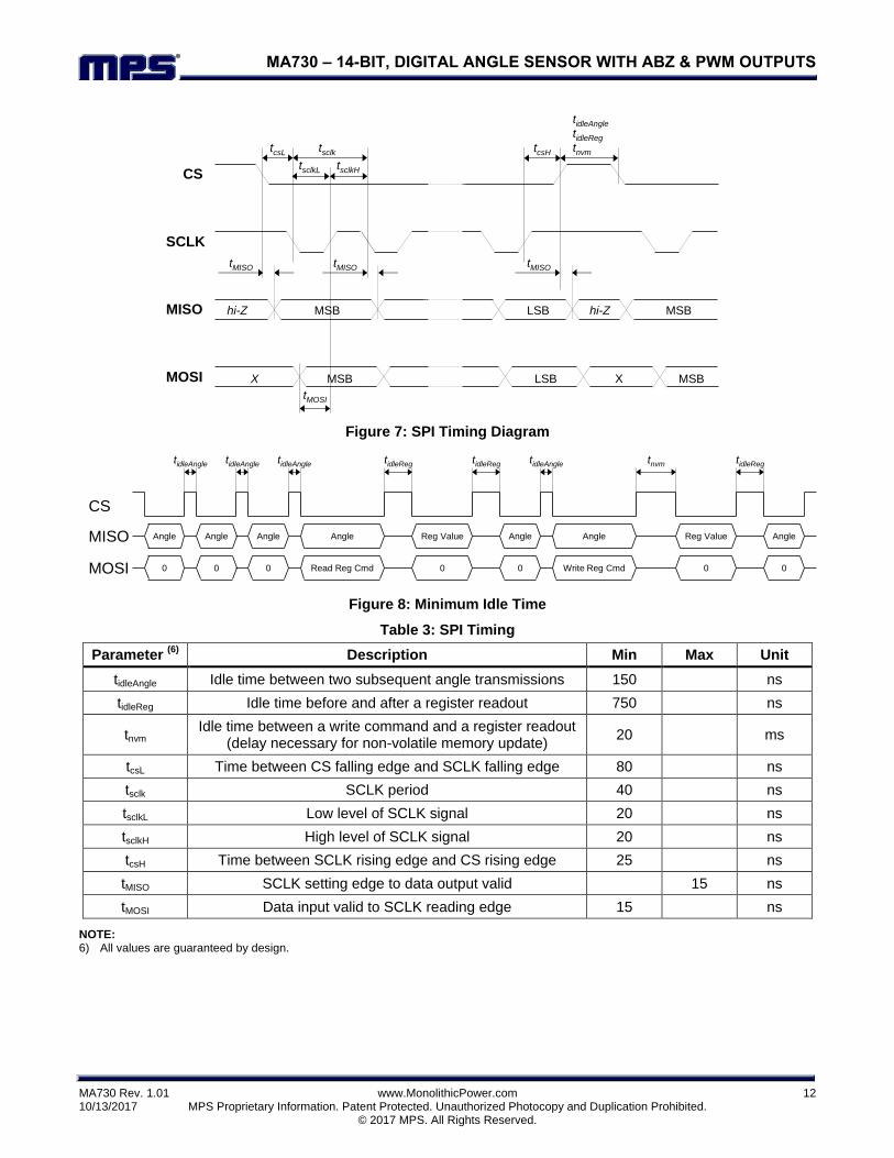
SPI is a four-wire, synchronous, serial communication interface. The MagAlpha supports SPI Mode 3 and Mode 0 (see Table 1 and Table 2). The SPI Mode (0 or 3) is detected automatically by the sensor and therefore does not require any action from the user. The maximum clock rate supported on SPI is 25MHz. There is no minimum clock rate. Note that real-life data rates depend on the PCB layout quality and signal trace length. See Figure 7 and Table 3 for SPI timing.
All commands to the MagAlpha (whether for writing or reading register content) must be transferred through the SPI MOSI pin and must be 16 bits long. See the SPI Communication section on page 13 for details.
Table 1: SPI Specification
Mode 0 Mode 3
SCLK idle state Low High
Data capture On SCLK rising edge
Data transmission On SCLK falling edge
CS idle state High
Data order MSB first
Table 2: SPI Standard
Mode 0 Mode 3
CPOL 0 1
CPHA 0 1
Data order (DORD) 0 (MSB first)
MA730 – 14-BIT, DIGITAL ANGLE SENSOR WITH ABZ & PWM OUTPUTS
MA730 Rev. 1.01 www.MonolithicPower.com 12 10/13/2017 MPS Proprietary Information. Patent Protected. Unauthorized Photocopy and Duplication Prohibited. © 2017 MPS. All Rights Reserved.
X
hi-Z
MSB
MSBLSBhi-Z
CS
SCLK
MOSI
MISO
LSB
tidleAngle
tidleReg
tnvmtcsL tsclk
tMISO
tMOSI
tsclkL tsclkH
tcsH
tMISO tMISO
MSB
MSB
X
Figure 7: SPI Timing Diagram
CS
MISO
MOSI
tidleAngle
Angle Angle Angle Reg Value
Read Reg Cmd
tidleReg tnvm
AngleAngle Angle
Write Reg Cmd0 000 0
Reg Value
0
tidleReg
Angle
tidleReg
0
tidleAngle tidleAngle tidleAngle
Figure 8: Minimum Idle Time
Table 3: SPI Timing
Parameter (6)
Description Min Max Unit
tidleAngle Idle time between two subsequent angle transmissions 150 ns
tidleReg Idle time before and after a register readout 750 ns
tnvm Idle time between a write command and a register readout
(delay necessary for non-volatile memory update) 20 ms
tcsL Time between CS falling edge and SCLK falling edge 80 ns
tsclk SCLK period 40 ns
tsclkL Low level of SCLK signal 20 ns
tsclkH High level of SCLK signal 20 ns
tcsH Time between SCLK rising edge and CS rising edge 25 ns
tMISO SCLK setting edge to data output valid 15 ns
tMOSI Data input valid to SCLK reading edge 15 ns
NOTE: 6) All values are guaranteed by design.

MA730 – 14-BIT, DIGITAL ANGLE SENSOR WITH ABZ & PWM OUTPUTS
MA730 Rev. 1.01 www.MonolithicPower.com 13 10/13/2017 MPS Proprietary Information. Patent Protected. Unauthorized Photocopy and Duplication Prohibited. © 2017 MPS. All Rights Reserved.
SPI Communication
The sensor supports three types of SPI operation:
Read angle
Read configuration register
Write configuration register
Each operation has a specific frame structure described below.
SPI Read Angle
Every 1µs, new data is transferred into the output buffer. The master device triggers the reading by pulling CS low.
When a trigger event is detected, the data remains in the output buffer until the CS signal is de-asserted (see Table 4).
Table 4: Sensor Data Timing
Event Action
CS falling edge Start reading and freeze
output buffer
CS rising edge Release of the output buffer
See Figure 9 for a diagram of a full SPI angle reading. See Figure 10 for a partial SPI angle reading. A full angle reading requires 16 clock pulses. The sensor MISO line returns:
MSB LSB
MISO Angle(15:0)
MOSI 0
The MagAlpha family has sensors with different features and levels of resolution. See the data output length section in the General Characteristics table on page 5 for the number of useful bits delivered at the serial output. If the data length is smaller than 16, the rest of the bits sent are zeros. For example, a data output length of 12 bits means that the serial output delivers a 12-bit angle value with four bits of zeros padded at the end (MISO state remains zero). If the master sends 16 clock counts, the MagApha replies with:
MSB LSB
MISO Angle(15:4) 0 0 0 0
MOSI 0
Angle reading can be therefore optimized without any loss of information by reducing the number of clock counts. In the case of a 12-bit data output length, only 12 clock counts are required to get the full sensor resolution.
MSB LSB
MISO Angle(15:4)
MOSI 0
If less resolution is needed, the angle can be read by sending even fewer clock counts (since the MSB is first).
In case of fast reading, the MagAlpha continues sending the same data until the data is refreshed. See the refresh rate section in the General Characteristics table on page 5.
Figure 9: Diagram of a Full 16-Bit SPI Angle Reading
Figure 10: Diagram of a Partial 8-Bit SPI Angle Reading
MA730 – 14-BIT, DIGITAL ANGLE SENSOR WITH ABZ & PWM OUTPUTS
MA730 Rev. 1.01 www.MonolithicPower.com 14 10/13/2017 MPS Proprietary Information. Patent Protected. Unauthorized Photocopy and Duplication Prohibited. © 2017 MPS. All Rights Reserved.
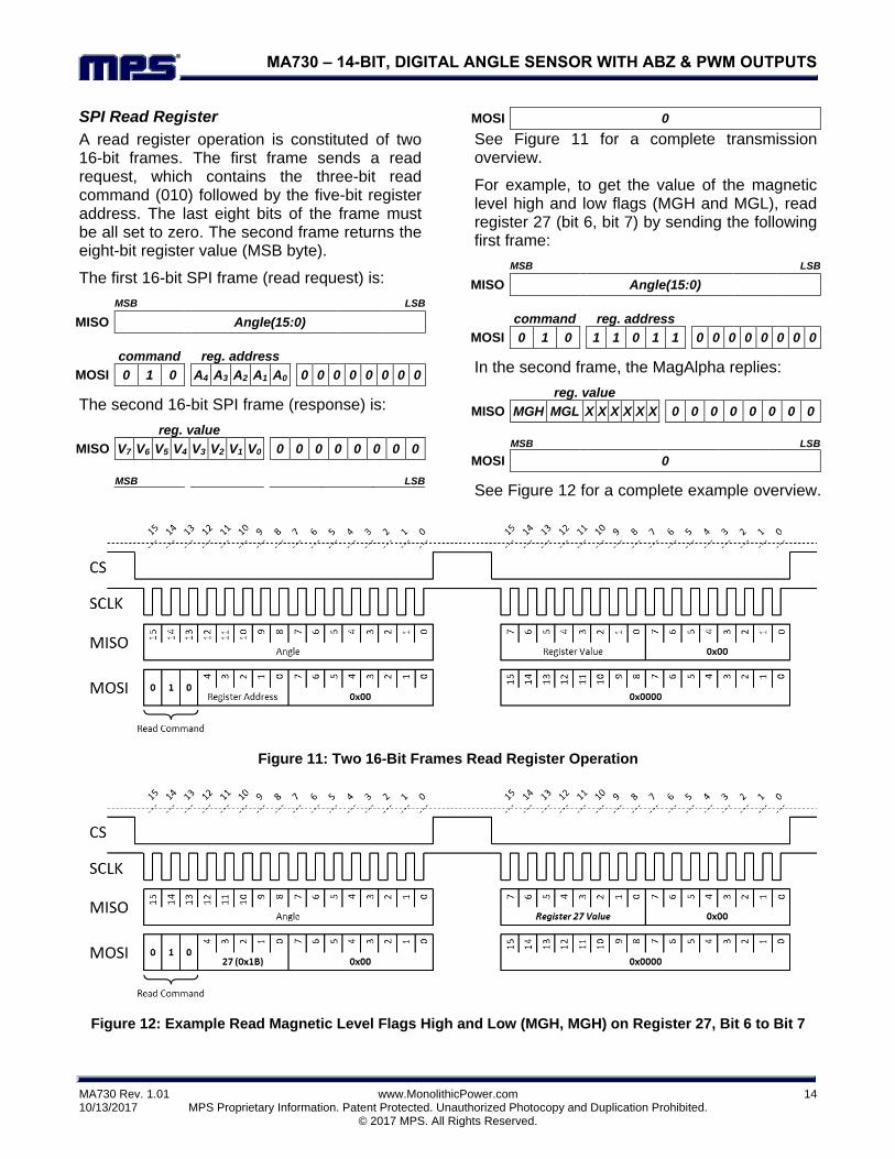
SPI Read Register
A read register operation is constituted of two 16-bit frames. The first frame sends a read request, which contains the three-bit read command (010) followed by the five-bit register address. The last eight bits of the frame must be all set to zero. The second frame returns the eight-bit register value (MSB byte).
The first 16-bit SPI frame (read request) is:
MSB LSB
MISO Angle(15:0)
command reg. address
MOSI 0 1 0 A4 A3 A2 A1 A0 0 0 0 0 0 0 0 0
The second 16-bit SPI frame (response) is:
reg. value
MISO V7 V6 V5 V4 V3 V2 V1 V0 0 0 0 0 0 0 0 0
MSB LSB
MOSI 0
See Figure 11 for a complete transmission overview.
For example, to get the value of the magnetic level high and low flags (MGH and MGL), read register 27 (bit 6, bit 7) by sending the following first frame:
MSB LSB
MISO Angle(15:0)
command reg. address
MOSI 0 1 0 1 1 0 1 1 0 0 0 0 0 0 0 0
In the second frame, the MagAlpha replies:
reg. value
MISO MGH MGL X X X X X X 0 0 0 0 0 0 0 0
MSB LSB
MOSI 0
See Figure 12 for a complete example overview.
Figure 11: Two 16-Bit Frames Read Register Operation
Figure 12: Example Read Magnetic Level Flags High and Low (MGH, MGH) on Register 27, Bit 6 to Bit 7
MA730 – 14-BIT, DIGITAL ANGLE SENSOR WITH ABZ & PWM OUTPUTS
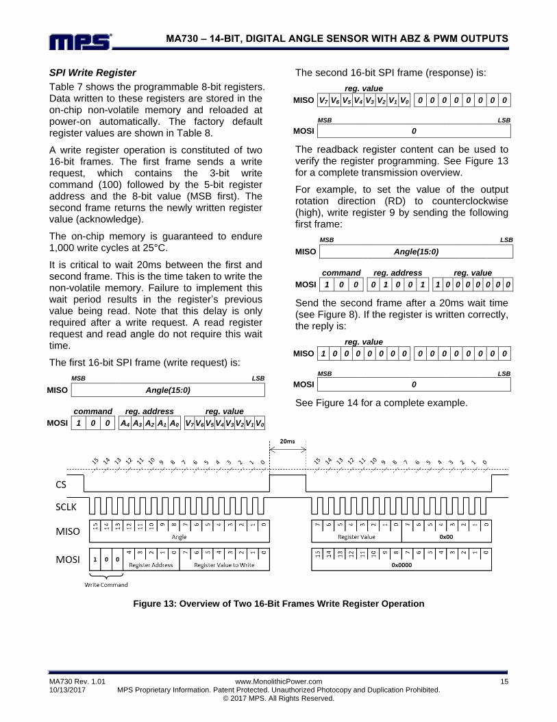
MA730 Rev. 1.01 www.MonolithicPower.com 15 10/13/2017 MPS Proprietary Information. Patent Protected. Unauthorized Photocopy and Duplication Prohibited. © 2017 MPS. All Rights Reserved.
SPI Write Register
Table 7 shows the programmable 8-bit registers. Data written to these registers are stored in the on-chip non-volatile memory and reloaded at power-on automatically. The factory default register values are shown in Table 8.
A write register operation is constituted of two 16-bit frames. The first frame sends a write request, which contains the 3-bit write command (100) followed by the 5-bit register address and the 8-bit value (MSB first). The second frame returns the newly written register value (acknowledge).
The on-chip memory is guaranteed to endure 1,000 write cycles at 25°C.
It is critical to wait 20ms between the first and second frame. This is the time taken to write the non-volatile memory. Failure to implement this wait period results in the register’s previous value being read. Note that this delay is only required after a write request. A read register request and read angle do not require this wait time.
The first 16-bit SPI frame (write request) is:
MSB LSB
MISO Angle(15:0)
command reg. address reg. value
MOSI 1 0 0 A4 A3 A2 A1 A0 V7 V6 V5 V4 V3 V2 V1 V0
The second 16-bit SPI frame (response) is:
reg. value
MISO V7 V6 V5 V4 V3 V2 V1 V0 0 0 0 0 0 0 0 0
MSB LSB
MOSI 0
The readback register content can be used to verify the register programming. See Figure 13 for a complete transmission overview.
For example, to set the value of the output rotation direction (RD) to counterclockwise (high), write register 9 by sending the following first frame:
MSB LSB
MISO Angle(15:0)
command reg. address reg. value
MOSI 1 0 0 0 1 0 0 1 1 0 0 0 0 0 0 0
Send the second frame after a 20ms wait time (see Figure 8). If the register is written correctly, the reply is:
reg. value
MISO 1 0 0 0 0 0 0 0 0 0 0 0 0 0 0 0
MSB LSB
MOSI 0
See Figure 14 for a complete example.
Figure 13: Overview of Two 16-Bit Frames Write Register Operation

MA730 – 14-BIT, DIGITAL ANGLE SENSOR WITH ABZ & PWM OUTPUTS
MA730 Rev. 1.01 www.MonolithicPower.com 16 10/13/2017 MPS Proprietary Information. Patent Protected. Unauthorized Photocopy and Duplication Prohibited. © 2017 MPS. All Rights Reserved.
Figure 14: Example Write Output Rotation Direction (RD) to Counterclockwise (High), on Register 9, Bit 7
SSI
SSI is a 2-wire synchronous serial interface for data reading only. The sensor operates as a slave to the external SSI master and supports only angle reading. It is not possible to read or write registers using SSI.
SSI Communication
Unlike SPI, the sensor SSI only supports angle reading operation. It is not possible to read or write registers using SSI. The SSI timing communication is shown in Figure 15 and Table 5.
Figure 15: SSI Timing
Table 5: SSI Timing
Parameter Description Min Max Unit
tssd 15 ns
tssck SSCK period 0.04 16 µs
tssckL Low level of SSCK signal 0.02 8 µs
tssckH High level of SSCK signal 0.02 8 µs
tm Transfer timeout (monoflop time) 25 µs
tp Dead time: SSCK high time for next data reading 40 µs
SSI Read Angle
The bit order of the transmitted data is MSB first and LSB last. Every 1µs, new data is transferred into the output buffer. The master device triggers the reading by driving SSCK high. A full reading requires up to 17 clock counts (see Figure 16).
The first clock is a dummy clock to start the transmission. The data length is up to 16 bits long. See the data output length section in the General Characteristics table on page 5 for the number of useful bits delivered at the serial output.

MA730 – 14-BIT, DIGITAL ANGLE SENSOR WITH ABZ & PWM OUTPUTS
MA730 Rev. 1.01 www.MonolithicPower.com 17 10/13/2017 MPS Proprietary Information. Patent Protected. Unauthorized Photocopy and Duplication Prohibited. © 2017 MPS. All Rights Reserved.
The first data MSB is transmitted on the second clock count. If the data length is less than 16, the 16-bit output word is completed by zeros. Therefore, the reading can also be performed with fewer than 16 clock counts. For example, for a part with a 12-bit data length, it is only necessary to send the first dummy clock to start the transmission plus 12 clocks to read the angle data.
When a trigger event is detected, the data remains in the output buffer until the clock falling edge for the LSB bit 0 and the transfer timeout time has passed (see Table 6).
Table 6: Sensor Data Timing
Trigger event Release of the output buffer
First SSCK pulse rising edge
SSCK falling edge + time out tm (Fig 15)
Figure 16: Diagram of a Full 16-Bit SSI Angle Reading (with First Dummy Clock)
For consecutive angle readings, see the timing diagram in Figure 17.
Figure 17: Diagram of Two Consecutive 16-Bit SSI Angle Reading with the Required Dead Time between the Frames

MA730 – 14-BIT, DIGITAL ANGLE SENSOR WITH ABZ & PWM OUTPUTS
MA730 Rev. 1.01 www.MonolithicPower.com 18 10/13/2017 MPS Proprietary Information. Patent Protected. Unauthorized Photocopy and Duplication Prohibited. © 2017 MPS. All Rights Reserved.
REGISTER MAP
Table 7: Register Map
No Hex Bin Bit 7 MSB
Bit 6 Bit 5 Bit 4 Bit 3 Bit 2 Bit 1 Bit 0 LSB
0 0x0 00000 Z(7:0)
1 0x1 00001 Z(15:8)
2 0x2 00010 BCT(7:0)
3 0x3 00011 - - - - - - ETY ETX
4 0x4 00100 PPT(1:0) ILIP(3:0) - -
5 0x5 00101 PPT(9:2)
6 0x6 00110 MGLT(2:0) MGHT(2:0) - -
9 0x9 01001 RD - - - - - - -
27 0x1B 11011 MGH MGL - - - - - -
Table 8: Factory Default Values
No Hex Bin Bit 7 MSB
Bit 6 Bit 5 Bit 4 Bit 3 Bit 2 Bit 1 Bit 0 LSB
0 0x0 00000 0 0 0 0 0 0 0 0
1 0x1 00001 0 0 0 0 0 0 0 0
2 0x2 00010 0 0 0 0 0 0 0 0
3 0x3 00011 0 0 0 0 0 0 0 0
4 0x4 00100 1 1 0 0 0 0 0 0
5 0x5 00101 1 1 1 1 1 1 1 1
6 0x6 00110 0 0 0 1 1 1 0 0
9 0x9 01001 0 0 0 0 0 0 0 0
Table 9: Programming Parameters
Parameters Symbol Number of
Bits Description See Table
Zero setting Z 16 Set the zero position 10
Bias current trimming
BCT 8 For side-shaft configuration: reduce the
bias current of the X or Y Hall device 13
Enable trimming X ETX 1 Biased current trimmed in the X direction
Hall device 14
Enable trimming Y ETY 1 Biased current trimmed in the Y direction
Hall device 14
Pulses per turn PPT 10 Number of pulses per turn of the ABZ
output 17
Index length / index position
ILIP 4 Parametrization of the ABZ index pulse Fig 26
Magnetic field high threshold
MGHT 3 Sets the field strength high threshold 16
Magnetic field low threshold
MGLT 3 Sets the field strength low threshold 16
Rotation direction RD 1 Determines the sensor positive direction 12

MA730 – 14-BIT, DIGITAL ANGLE SENSOR WITH ABZ & PWM OUTPUTS
MA730 Rev. 1.01 www.MonolithicPower.com 19 10/13/2017 MPS Proprietary Information. Patent Protected. Unauthorized Photocopy and Duplication Prohibited. © 2017 MPS. All Rights Reserved.
REGISTER SETTINGS Zero Setting
The zero position of the MagAlpha (a0 ) can
be programmed with 16 bits of resolution. The angle streamed out by the MagAlpha (aout) is given by Equation (2):
0aaa rawout (2)
Where araw is the raw angle provided by the MagAlpha front-end.
The parameter Z(15:0), which is zero by default, is the complementary angle of the zero setting. It can be written in decimals using Equation (3):
)0:15(216
0 Za (3)
Table 10 shows the zero setting parameter.
Table 10: Zero Setting Parameter
Z(15:0) Zero pos.
a0 16-bit (dec) Zero pos. a0 (deg)
0 65536 360.000
1 65535 359.995
2 65534 359.989
… … …
65534 2 0.011
65535 1 0.005
Example
To set the zero position to 20 degrees, the Z(15:0) parameter must be equal to the complementary angle and can be calculated with Equation (4):
618952deg360
deg202)0:15( 1616 Z (4)
In binary, this is written as 1111 0001 1100 0111.
Table 11 shows the content of registers 0 and 1.
Table 11: Register 0 and 1 Content
Reg Bit 7 Bit 6 Bit 5 Bit 4 Bit 3 Bit 2 Bit 1 Bit 0
0 1 1 0 0 0 1 1 1
1 1 1 1 1 0 0 0 1
Rotation Direction
By default, when looking at the top of the package, the angle increases when the magnetic field rotates clockwise (CW) (see Figure 18 and Table 12).
Figure 18: Positive Rotation Direction of the Magnetic Field
Table 12: Rotation Direction Parameter
RD Positive Direction
0 Clockwise (CW)
1 Counterclockwise (CCW)
BCT Settings (Bias Current Trimming)
Side Shaft
When the MA730 is mounted on the side of the magnet, the relation between the field angle and the mechanical angle is no longer directly linear. This effect is related to the fact that the tangential magnetic field is usually smaller than the radial field. Define the field ratio k with Equation (5):
tan/ BBk rad (5)
Where Brad and Btan are the maximum radial and tangential magnetic fields (see Figure 19).
Figure 19: Side-Shaft Field

MA730 – 14-BIT, DIGITAL ANGLE SENSOR WITH ABZ & PWM OUTPUTS
MA730 Rev. 1.01 www.MonolithicPower.com 20 10/13/2017 MPS Proprietary Information. Patent Protected. Unauthorized Photocopy and Duplication Prohibited. © 2017 MPS. All Rights Reserved.
The ratio k depends on the magnet geometry and the distance to the sensor. Having a k ratio different from one results in the sensor output response not being linear with respect to the mechanical angle. Note that the error curve has the shape of a double sinewave (see Figure 21). E is the amplitude of this error.
The X-axis or the Y-axis bias current can be reduced in order to recover an equal Hall signal for all angles and therefore suppress the error. The parameters ETX and ETY control the direction in which sensitivity is reduced. The current reduction is set by the parameter bias current trimming BCT(7:0), which is an integer from 0 to 255.
In side-shaft configuration (i.e.: the sensor center is located beyond the magnet outer diameter), k is greater than one. For optimum compensation, the sensitivity of the radial axis should be reduced by setting the BCT parameter as shown in Equation (6):
kBCT
11258)0:7( (6)
The graph in Figure 20 shows the optimum BCT value for a particular k ratio.
0
50
100
150
200
1 1.5 2 2.5 3 3.5 4 4.5 5
BC
T
k
Figure 20: Relation between the k Ratio and the Optimum BCT to Recover Linearity
Table 13 shows some typical BCT values.
Table 13: Example of BCT Settings
E (deg) Magnet Ratio (k) BCT(7:0)
0 1.0 0
11.5 1.5 86
19.5 2.0 129
25.4 2.5 155
30.0 3.0 172
33.7 3.5 184
36.9 4.0 194
39.5 4.5 201
41.8 5.0 207
Determining k with the MagAlpha
It is possible to deduce the k ratio from the error curve obtained with the default BCT setting (BCT = 0). For this purpose, rotate the magnet over one revolution and record the MagAlpha output. Then plot the error curve (the MagAlpha output minus the real mechanical position vs. the real mechanical position) and extract two parameters: the maximum error (E) and the position of this maximum with respect to a zero crossing am (see Figure 21). k can be calculated with Equation (7):
)tan(
)tan(
m
m
a
aEk
(7)
-40
-20
0
20
40
0 50 100 150 200 250 300 350
Err
or
(deg
)
m
rotor angle (deg)
2E
Figure 21: Error Curve in Side-Shaft Configuration with BCT = 0
Some examples are given in Table 13. Alternatively, the k parameter can be obtained from the graph in Figure 22.
MA730 – 14-BIT, DIGITAL ANGLE SENSOR WITH ABZ & PWM OUTPUTS
MA730 Rev. 1.01 www.MonolithicPower.com 21 10/13/2017 MPS Proprietary Information. Patent Protected. Unauthorized Photocopy and Duplication Prohibited. © 2017 MPS. All Rights Reserved.
1
1.5
2
2.5
3
3.5
4
4.5
5
0 5 10 15 20 25 30 35 40
k
E (deg)
Figure 22: Relation between the Error Measured with BCT = 0 and the Magnet Ratio k
Sensor Orientation
The dot marked on the package shows whether the radial field is aligned with the sensor coordinate X or Y (see Figure 23).
Figure 23: Package Top View with X and Y Axes
Determine which axis needs to be reduced (see the qualitative field distribution around a ring in Figure 19). For instance, with the arrangement depicted in Figure 23, the field along the sensor Y direction is tangential and weaker. The X-axis should be reduced (ETX = 1 and ETY = 0). Note that if both ETX and ETY are set to 1, the current bias is reduced in both directions the same way (i.e.: without side-shaft correction) (see Table 14).
Table 14: Trimming Direction Parameters
ETX Enable Trimming of the X Axis
0 Disabled
1 Enabled
ETY Enable Trimming of the Y Axis
0 Disabled
1 Enabled
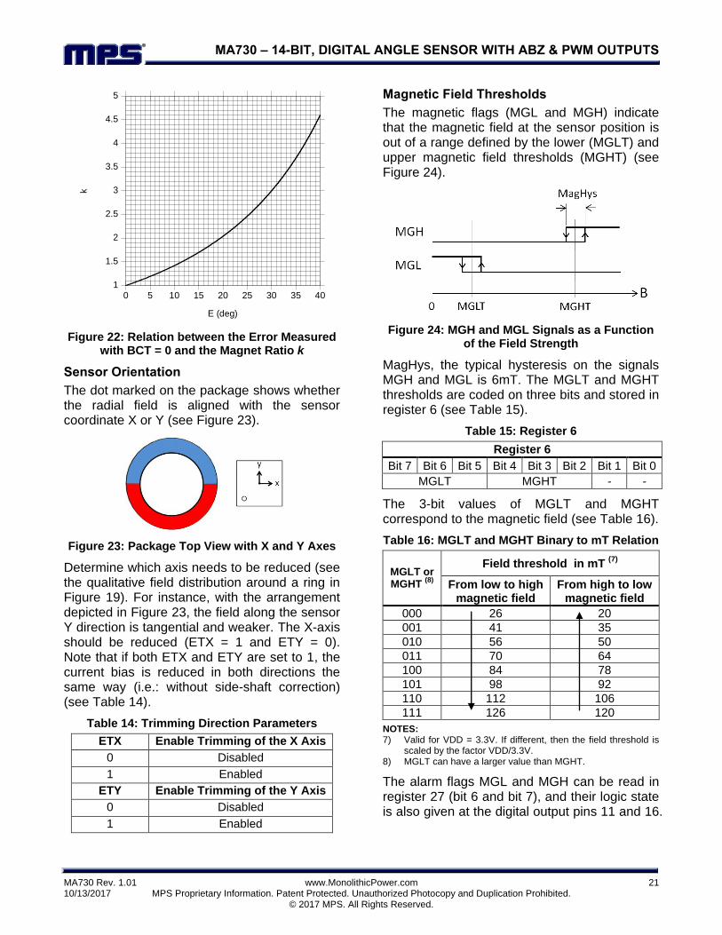
Magnetic Field Thresholds
The magnetic flags (MGL and MGH) indicate that the magnetic field at the sensor position is out of a range defined by the lower (MGLT) and upper magnetic field thresholds (MGHT) (see Figure 24).
Figure 24: MGH and MGL Signals as a Function of the Field Strength
MagHys, the typical hysteresis on the signals MGH and MGL is 6mT. The MGLT and MGHT thresholds are coded on three bits and stored in register 6 (see Table 15).
Table 15: Register 6
Register 6
Bit 7 Bit 6 Bit 5 Bit 4 Bit 3 Bit 2 Bit 1 Bit 0
MGLT MGHT - -
The 3-bit values of MGLT and MGHT correspond to the magnetic field (see Table 16).
Table 16: MGLT and MGHT Binary to mT Relation
MGLT or MGHT
(8)
Field threshold in mT (7)
From low to high magnetic field
From high to low magnetic field
000 26 20
001 41 35
010 56 50
011 70 64
100 84 78
101 98 92
110 112 106
111 126 120
NOTES: 7) Valid for VDD = 3.3V. If different, then the field threshold is
scaled by the factor VDD/3.3V. 8) MGLT can have a larger value than MGHT.
The alarm flags MGL and MGH can be read in register 27 (bit 6 and bit 7), and their logic state is also given at the digital output pins 11 and 16.

MA730 – 14-BIT, DIGITAL ANGLE SENSOR WITH ABZ & PWM OUTPUTS
MA730 Rev. 1.01 www.MonolithicPower.com 22 10/13/2017 MPS Proprietary Information. Patent Protected. Unauthorized Photocopy and Duplication Prohibited. © 2017 MPS. All Rights Reserved.
To read the MGL and MGH flags by SPI send the 8-bit command write into register 27:
command reg. address MSB value LSB
0 1 0
1 1 0 1 1
0 0 0 0 0 0 0 0
The MA730 answers with the register 27 content in the next transmission:
R[7:0]
MGH MGL x x x x x x
ABZ Incremental Encoder Output
The MA730 ABZ output emulates a 12-bit incremental encoder (such as an optical encoder) providing logic pulses in quadrature (see Figure 25). Compared to signal A, signal B is shifted by a quarter of the pulse period. Over one revolution, signal A pulses n times, where n is programmable from 1 to 1024 pulses per revolution. The number of pulses per channel per revolution is programmed by setting the parameter PPT, which consists of eight bits split between registers 0x4 and 0x5 (see Table 7). The factory default value is 1023. Table 17 describes how to program PPT(9:0) to set the required resolution.
Table 17: PPT
PPT(9:0) Pulses per Revolution
Edges per Revolution
0000000000 1 4 MIN
0000000001 2 8
0000000010 3 12
0000000011 4 16
… … … …
1111111100 1021 4084
1111111101 1022 4088
1111111110 1023 4092
1111111111 1024 4096 MAX
For example, to set 120 pulses per revolution (i.e.: 480 edges), set PPT to 120 - 1 = 119 (binary: 0001110111). Registers 4 and 5 must be set as shown in Table 18.
Table 18: Example PPT Setting for 120 Pulses
B7 B6 B5 B4 B3 B2 B1 B0
R4 1 1 0 0 0 0 0 0
R5 0 0 0 1 1 1 0 1
Figure 25: Timing of the ABZ Output
Signal Z (zero or index) raises only once per turn at the zero-angle position.
The position and length of the Z pulse is programmable via bits ILIP[3:0] in register 0x5 (see Figure 26).
Figure 26: ILIP Parameter Effect on Index Shape
By default, the ILIP parameter is 0000. The index rising edge is aligned with the channel B falling edge. The index length is half the A or B pulse length.
ABZ Hysteresis
A hysteresis larger than the output noise is introduced on the ABZ output to prevent any spurious transitions (see Figure 27).
Figure 27: Hysteresis of the Incremental Output
MA730 – 14-BIT, DIGITAL ANGLE SENSOR WITH ABZ & PWM OUTPUTS
MA730 Rev. 1.01 www.MonolithicPower.com 23 10/13/2017 MPS Proprietary Information. Patent Protected. Unauthorized Photocopy and Duplication Prohibited. © 2017 MPS. All Rights Reserved.
ABZ Jitter
The ABZ state is updated at a frequency of 16MHz, enabling accurate operation up to a very high rpm (above 105 rpm).
The jitter characterizes how far a particular ABZ edge can occur at an angular position different from the ideal position (see Figure 28).
Figure 28: ABZ Jitter
The measurable jitter is composed by a systematic jitter (i.e.: always the same deviation at a given angle) and a random jitter.
The random jitter reflects the sensor noise. Therefore, the edge distribution is the same as the SPI output noise. Like the sensor resolution, it is defined as the 3σ width of this distribution.
In fact, the random jitter is a function of the rotation speed. At a lower speed, the random jitter is smaller than the sensor noise.
This is a consequence of the fact that the probability of measuring an edge at a certain distance from the ideal position depends on the number of ABZ updates at this position.
The minimum field for ABZ reading is 40mT.
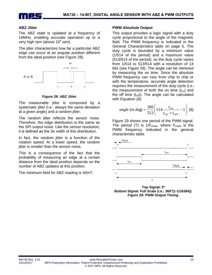
PWM Absolute Output
This output provides a logic signal with a duty cycle proportional to the angle of the magnetic field. The PWM frequency is indicated in the General Characteristics table on page 5. The duty cycle is bounded by a minimum value (1/514 of the period) and a maximum value (513/514 of the period), so the duty cycle varies from 1/514 to 513/514 with a resolution of 14 bits (see Figure 29). The angle can be retrieved by measuring the on time. Since the absolute PWM frequency can vary from chip to chip or with the temperature, accurate angle detection requires the measurement of the duty cycle (i.e.: the measurement of both the on time (ton) and the off time (toff)). The angle can be calculated with Equation (8):
1514
512
360deg)(
OFFON
ON
tt
tinangle (8)
Figure 29 shows one period of the PWM signal. The period (T) is 1/FPWM, where FPWM is the PWM frequency indicated in the general characteristic table.
T/514
T
T/514
tON
tOFF
Top Signal: 0° Bottom Signal: Full Scale (i.e.: 360°(1-1/16384))
Figure 29: PWM Output Timing

MA730 – 14-BIT, DIGITAL ANGLE SENSOR WITH ABZ & PWM OUTPUTS
MA730 Rev. 1.01 www.MonolithicPower.com 24 10/13/2017 MPS Proprietary Information. Patent Protected. Unauthorized Photocopy and Duplication Prohibited. © 2017 MPS. All Rights Reserved.
TYPICAL APPLICATION CIRCUITS
Figure 30: Typical Configurations Using SPI Interface and MGH/MGL Signals
Figure 31: Typical Configuration Using ABZ Interface

MA730 – 14-BIT, DIGITAL ANGLE SENSOR WITH ABZ & PWM OUTPUTS
MA730 Rev. 1.01 www.MonolithicPower.com 25 10/13/2017 MPS Proprietary Information. Patent Protected. Unauthorized Photocopy and Duplication Prohibited. © 2017 MPS. All Rights Reserved.
PACKAGE INFORMATION
QFN-16 (3mmx3mm)
MA730 – 14-BIT, DIGITAL ANGLE SENSOR WITH ABZ & PWM OUTPUTS
MA730 Rev. 1.01 www.MonolithicPower.com 26 10/13/2017 MPS Proprietary Information. Patent Protected. Unauthorized Photocopy and Duplication Prohibited. © 2017 MPS. All Rights Reserved.
APPENDIX A: DEFINITIONS Effective Resolution (3σ noise level)
Smallest angle increment distinguishable from the noise. The resolution is measured by computing three times σ (the standard deviation in degrees) taken over 1,000 data points at a constant position. The resolution in bits is obtained with log2(360/6σ).
Refresh Rate Rate at which new data points are stored in the output buffer.
ABZ Update Rate Rate at which a new ABZ state is computed. The inverse of this rate is the minimum time between two ABZ edges.
Latency
Time elapsed between the instant when the data is ready to be read and the instant at which the shaft passes that position. The lag in degrees is
vlatencylag , where v is the angular velocity in deg/s.
Power-Up Time Time until the sensor delivers valid data starting at power-up.
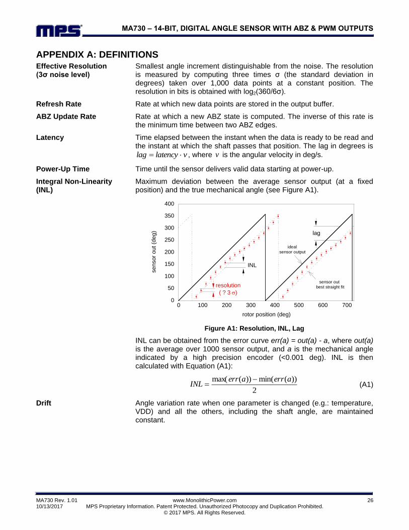
Integral Non-Linearity (INL)
Maximum deviation between the average sensor output (at a fixed position) and the true mechanical angle (see Figure A1).
0
50
100
150
200
250
300
350
400
0 100 200 300 400 500 600 700
se
nsor
out
(de
g)
rotor position (deg)
resolution
( ? 3 )
idealsensor output
INL
lag
sensor out
best straight fit
Figure A1: Resolution, INL, Lag
INL can be obtained from the error curve err(a) = out(a) - a, where out(a) is the average over 1000 sensor output, and a is the mechanical angle indicated by a high precision encoder (<0.001 deg). INL is then calculated with Equation (A1):
2
))(min())(max( aerraerrINL
(A1)
Drift Angle variation rate when one parameter is changed (e.g.: temperature, VDD) and all the others, including the shaft angle, are maintained constant.

MA730 – 14-BIT, DIGITAL ANGLE SENSOR WITH ABZ & PWM OUTPUTS
NOTICE: The information in this document is subject to change without notice. Users should warrant and guarantee that third party Intellectual Property rights are not infringed upon when integrating MPS products into any application. MPS will not assume any legal responsibility for any said applications.
MA730 Rev. 1.01 www.MonolithicPower.com 27 10/13/2017 MPS Proprietary Information. Patent Protected. Unauthorized Photocopy and Duplication Prohibited. © 2017 MPS. All Rights Reserved.
APPENDIX B: SPI COMMUNICATION CHEATSHEET Read Angle
Read Register
Write Register

Mouser Electronics
Authorized Distributor
Click to View Pricing, Inventory, Delivery & Lifecycle Information: Monolithic Power Systems (MPS):
MA730GQ-P MA730GQ-Z


