R-51794 WIDEBAND FIBER OPTIC CONNUNICATIONS LINK(U) AIR FORCE 1/INST OF TECH WRIGHT-PRTTERSON AFB ON SCHOOL OFENGINEERING J R BRAY DEC 84 RFIT/GE/ENG/84D-16
-5UNCLASFIEF/O 112NL
E70000E00000EEEmmhmhhhmhlEomhmhmhmhhumEhohmhhhEEmhhIEEEEEEEEmhEmhElmosomhohEEmhEI

. . . .. 7 .•1111• 9 g•j•J•j-)
°°ll
*.JJj° i 11
klhI

WIDEBAND FIBER OPTIC
COMMUNICATIONS LINK.-
THESIS
James R. BrayFirst Lieutenant, USAF
AFIT/GE/ENG/84D-1 6IDTIC
AppoT vW IO N public E N ' Wo -o" lE CTi" "MAR 2/ 8 1985
O I FC-3 ~ DEANT OFIBE R OCE
Wright-Patterson Air Force Base, Ohio
•.85 03 13 135~~~3SldXS lN41 Nkl3AOO,lJV w3nu1OUdau:
-.....: ..- :..--. .- . . .. . . . .. . ..F.I..../G..E/...E.NG./,8. ..4D...-.16. . .

AFIT/GE/ENG/84D-16
WIDEBAND FIBER OPTIC
COMMUNICATIONS LINK
THRE SIS
James R. BrayFirst Lieutenant, USAF
AFIT/GE/ENG/84D-16
WMP 2 8098
n Distaiuti~u nlii
AFIT/GE/ENG/84D-16
WIDEBAND FIBER OPTIC COMMUNICATIONS LINK
THESIS
Presented to the Faculty of the School of Engineering
of the Air Force Institute of Technology
Air University
In Partial Fulfillment of the
Requirements for the Degree of
Master of Science in Electrical Engineering
James R. Bray, B.S.
First Lieutenant, USAF
December 1984
Approved for public release; distribution unlimited
-.... .. . . . . . . . ...... .... ....... ... •-.. ...... •- =-

* -- -~..---.--... - 7... 7...
Preface
The purpose of this, %tudy was to design and implement
a single strand, full duplex, fiber optic communications link.
The finished system, complete with user's manual and schematics,
is to remain at the Air Force Institute of Technology for
future research and experimentation.
This fiber optic project demonstrates the ease and prac-
ticality of using fibers for ground based local or long haul
communications systems. However the first four references
listed in the bibliography show other uses, primarily on air-
craft systems, accenting potential use in a military environ-
ment.
0 Because of over eight years experience in both long line
and radio propagation communication systems I completed the
work on this project with great interest and enthusiasm. I
also believe that this type of project compliments and completes
the Optical Communications Course Sequence that I completed
at AFIT.
I would like to thank Major Kenneth C. Castor for sug-
gesting and allowing me to do this work, and Dr. Vaqar Syed
for the freedom to pursue my self imposed goals throughout the
project. Finally, I wish to thank my wife Conchi and my daugh-
ters, Elena and Sole, for their support and understanding
through these nine long months of this project.
James R. Bray
ii .
.. .. . .. . 7•. .. '--A

Table of Contents
Page
P reface........ ...... . , I o I I P V. I V . i
List of Figures .. .. . . .. . ... . v
List of Tables . . . . . . * . . .1 0 v i
Abstract................ . . . . . . ... vii
I. Introduction.......... .. . . .
Ii. Background Information , . . 3
Description of Available Equipment . 3Optical Fibers . . .. . . 14Emitters, Detectors and Connectors . . .. 29Experimental Measurements of the OpticalSystem................... 33
III. Problem Statement and Approach...........38
Problem........ ...... . . . . . . . . . . 38
'd Scope.................................., 38Approach ................. 39Material Required ................. 44Support Equipment...............44Additional Support Required.... ...... 44
jIV. System Implementation. ............. . . . 46
Component Removal ................ 46Control Circuit Design and Construction 47Cabinet Modifications.......... ... q 51Component Installation and FiberTerminations .................... 53
V. Fiber Testing and System Operation...........56
Fiber Tests....... .............. 56LED Emission Radiation Pattern o o 66 -
System Operational Testso.............69
VI. Conclusion..... ................... 75
Summary of Work .. .. . . .. . 75Problems Encountered..............78Recommendations.................78
Page
Appendix; -perations- !anua . ,. . , , , , , , , , 80
B ibliography . . . . , . . . .. , , . 94 .
Vita . * * * * * * * * 96
----
V.. .. ... . . . . ..... 6
....

List of Figures
Figure Page
I. SPX 1775 Output Intensity vs Radius . , , 10
2a. Ring Termination for LED Interface ...... 11 . -
2b. Circular Termination for Photodiode Interface 11
3. ITT Connector ... ................. 13
4. Radiance Power Beams of Surface Emitting andLaser Diode ....... .................. . 16
5. Optical Power Launching . . ........ 17
6. Axial Displacement ...... ................ 21
7. Longitudinal Separation .... ............. 23
8. Radiative Loss ...... .................. 27
9. Fiber Microbends .. .. . . . . . . 28
10. Optical Fiber Technologies, Inc., 200-S StyleA SMA Connector ...... ................. . 34
11. Setup for Measuring LED Emission Pattern 35
12. Logic Diagram of Control Circuit.... .... . 48..-..-.
13. Wiring Diagram of Control Circuit . ........ 50
14. Diagram of New Front Panel ... ........ ... 52
15a. Light Pattern With Good Cleave .. .......... 61
15b. Light Pattern of Broken -iber ... ........ 61
15c. Light Pattern of Angled Cleave ... ......... 62
15d. Light Pattern of Fiber With Angled Corner . 62
16. LED Emission Radiation Pattern .......... 68
17. Average Output Power vs Input Frequency , 74
V
...................................~.**.**.. .... ... ... .... ... ...
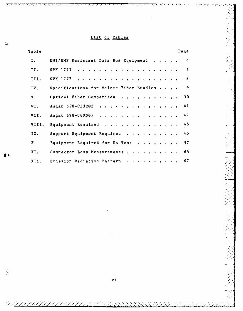
List of Tables
Table Page
I. EMI/EMP Resistant Data Bus Equipment ... 4
Ii. SPX 1775..................... 7
IV. Specifications for Valtec Fiber Bundles .. $ 9
V. Optical Fiber Comparison ., 30
VI. Augat 698-013EG2 0 . t i a 9 0 41
VII. Augat 698-069DG ................. 42
VIII. Equipment Required.... . . . ..... 45
IX. Support Equipment Required..............45
X. Equipment Required for NA Test ... 90v1 57
XI. Connector Loss Measurements .. .. .. ... .65
XII. Emission Radiation Pattern.............67
vi

AFIT/GE/ENG/84D-16
Abstract
A feasibility study was conducted on the possibility of
upgrading a nine port fiber optic bundle telecommunications
system to a single strand fiber optic system. Usable pieces
of equipment were identified and new Light Emitting Diodesi! ;)
Photodetectors and single strand SMA styled fiber optic con-
nectors were ordered. Background research was conducted in
the area of fiber optic power launching, fiber losses, connec-
tor losses and efficiences. A new modulation/demodulation
circuit was designed and constructed using parts from unused
equipment. A new front panel was constr&jcted to house the
components, switches and connectors. Aitwo meter piece of
optical fiber was terminated with the new connectors and tested
for connector loss, numeric aperture and attenuation. The ,
new Light Emitting Diod" was characterized by its emission
radiation pattern and the entire system was tested for func-
tional operation, frequency response and bandwidth of opera-
tion. An Operations Manual was prepared to ensure proper use
in the future. The result was a two piece, single strand, fi-
ber optic communications system fully TTL compatible, capable
of transmitting digital signals from 80 Kbit/sec to 20
Mbit/sec. The system was tested in a half duplex mode using
both baseband and carrier modulated signals. Utilizing both
pieces of the system full duplex operation was also demon-
strated.vii
-.1.
........................................................................,....'- . . .. . . :.-i.v ' i:, - ,, . -,.- ..-. .--. -: .: .. -.. '....* * * **...? -* .--- * *.*.-...?.-. . .. . .. ,i.? -? . .i-. .?. .....*. .? -:.?-*%. . . .
WIDEBAND FIBER OPTIC COMMUNICATIONS LINK
I. Introduction
In October, 1973, Spectronics, Inc. was contracted to
develop a program concerned with the design and fabrication
of an Electro-Magnetic Interference/Electro-Magnetic Pulse
Resistant Data Bus. The system was constructed as an opto-
electronic data bus and was compared to systems using twisted
pair, coaxial cable and waveguide communications media. The
system constructed used GaAs Light Emitting Diodes, flexible
Fiber Optic Bundles, Silicon PIN Photodiodes and passive
optical couplers. This fiber optic system was delivered to
the Air Force Avionics Laboratory at Wright-Patterson Air
Force Base in September, 1975. When the Avionics Lab fin-
ished their work with the system, all remaining equipment,
documents and schematics were given to the Air Force Insti-
tute of Technology for research and experimentation.
An investigation was conducted on the remaining equip-
ment from the Spectronics Dat'a Bus to determine the feasibil-
ity of upgrading the system to a single strand optical fiber
communications link. The investigation entailed determining
whether the system was operational or not, its protocol sys-
tem and the practicality of its coding scheme. The system's
electro-optic interface waa3 also checked for its compatibil-
ity with a single strand optical fiber. Research was con-
.."-.-..- -..- -.-..- --.-.--. ..... ... . '... . . .,'.". - ..-.- ,". .-.-. -...... '' .". .
...... <-.•

ducted on optical fibers themselves in the areas of power
launching techniques and efficiency, coupling loss, intrinsic
losses and bandwidth constraints.
It was determined that a single strand optical fiber
communications system could be implemented utilizing much of
the equipment provided by the Spectronics project with only
a few major changes. The original protocol and coding
schemes were not versatile enough and were to be eliminated
along with the existing electro-optic interface and fiber
optic bundles. New single strand fibers with standard con-
nectors were to be constructed and new Light Emitting Diodes
and Photodetectors were ordered to be installed on the cab-
inet. A modulation/demodulation circuit was to be designed
and constructed to provide a system capability of both base-
band and carrier modulation modes of transmission. The sys-
tem was designed to operate on digital signals at least as
fast as the original system, 10 Mbit/sec, Manchester NRZ
code.
Once implemented the system was to be tested at both the
component level and for overall system operation. Finally, a
user's manual was to be prepared to ensure proper use of the
new system in subsequent research and experimentation.
2

II. Background Information
Research for this project was conducted and is presented
in four major categories. First, a discussion on the feasi-
bility of upgrading some in-house available equipment from
fiber bundle to single strand fiber optic communications
media. Next, is a presentation of fiber optic power losses
and bandwidth considerations. This is followed by a discus-
sion of Light Emitting Diodes, Laser Diodes and Photodetec-
tors, and finally, a series of tests that can be .used to
characterize a completed fiber optic communications link and
its primary components.
Description of Available Equipment
In September, 1976, Technical Report AFAL-TR-76-99 was
submitted to the Air Force Avionics Laboratory along with all
equipment that comprised an Electro-Magnetic Interference/
Electro-Magnetic Pulse (EMI/EMP) Resistant Data Bus. This
system was designed using fiber optic bundle technoloy and
was completed by Spectronics, Inc., of Richardson, Texas.
When the Air Force Avionics Laboratory completed their
work with the EMI/EMP Resistant Data Bus the remaining equip-
ment was given 1- the Air Force Institute of Technology
(AFIT). Table I lists the equipment originally supplied by
Spectronics and also shows the quantities that remain on hand
at AFIT now. All remaining equipment and the final report are
now located and available, with schematics, in the
• . . .. • " " - . .. ' °° . . . o. " . . . " . " . . . .. . . . .-- •.,. .. , .. ... . .. . -.. .. °.. .•

-r44
100
IV-
to u$.J1.
-W 0
-r4~
Cou
Cun
17,

Surface Emitting Diode 5Q0 4Q0 300
/0 -200
/loo
\ o 180- 100
\ 'N
N. 2 0
Source Laser Diode
(11:12 0)
Figure 4. Radiance Power Beams of Surface Emittingand Laser Diode.
16

are normally modeled as pure Lambertian sources; however,
edge emitting LED's and laser diodes are somewhat more com-
plicated to model. Equations (1) and (2) below are the math-
ematical descriptions of the output radiance patterns of the
surface emitting and edge emitting LED's (11:120).
B(e,4) = B cose. (1)0
2 21 sin CosB =,6 L . (2)B cosT(e) B cos ()o 0
The term B is the maximum radiance emitted by the
source. The angles e and 4 are the same as those normally
defined in spherical coordinates. The terms T and L are the
transverse and lateral power distribution coefficients. For
edge emitting diodes, the (parameter) T of Equation (2) is
normally 1, while the (parameter) L is significantly larger.
Figure 4 is an example of both the surface emitting diode and
a laser diode output radiation patterns. The laser diode has
a half-power beam width of 10*, where L is approximately 180.
The magnitude of the laser diode has been greatly reduced in .
order to put both diagrams on the same chart.
An example of a theoretical calculation of the amount of
power that can be launched into a fiber will be shown with a
step index fiber as depicted in Figure 5. The amount of power
actually coupled to the fiber, Pf, can be determined from
Equation (3).
15

desirable because the 37 strand Valtec fiber bundle was
split with 19 strands for the transmit side and 18 strands
for the receive.
The optical fiber bundles for the EMI/EMP Data Bus were
interconnected with a nine port radial coupler. This optical
connector had the property of splitting the input signal from
any of the ports to all nine fiber bundles of the system.
The optical coupler is still intact, complete with test data
and connecting plug.
Also available at AFIT are three spools of single strand
optical fiber. One spool is identified with the part number -
ITT-T-1271-16. This fiber has a 50am core, 125Mm outer dia-
meter, Numeric Aperture (NA) of 0.2, parabolically graded
index of refraction, approximately 3 dB/Km loss and is about
200 meters in length. The other two spools have consider-
ably less fiber and are not marked with any identifying part
numbers.
Optical Fibers
Discussion on optical fibers will be limited to single
strand, multi-mode fibers, tleir power launching capabilities, -
power losses and bandwidth limitations. Then comparisons of
fibers on hand and some commercially available fibers will be
presented.
The amount of optical power that can be successfully
launched into a fiber is dependent not only on the fiber
itself, but also on the power source. Surface emitting LED's
14
-7- =°

DET EM.
.2 5
SPX 1777 Detector SPX 1775 Emitter
(1:36)
Figure 3. ITT Connector.
13
..

7. 7,
munications experiments.
Another severe limitation for the use of this system as
originally designed is that the MTU Test Sets were not deliv-
ered to AFIT as part of the package. At least one of these
test sets is essential because it generates a status word
back to the CMTU after the initial command word. Without
this status word, data transmission is prohibited by the
CMTU.
Lastly, the CMTU and the CMTU Test Set were checked for
circuit integrity and were found to be modified from their
original design. Specifically, the serial data stream line
from the parallel to serial convertor card to the LED driver/
amplifier card in the CMTU had been cut allowing a direct TTL
compatible input to the optical transmitter. Also, the data
stream line from the PD detector card to the signal condi-
tioning card had been cut allowing a direct TTL compatible
data line from the optical receiver. Further inspection of
the interface between the CMTU Test Set and the CMTU showed
that the command logic between these two components was not
functioning properly. When the CMTU would query the CMTU
Test Set for a specific response to set up a data transfer,
there was no response.
The LED's and PD's were mounted to the CMTU and MTU's
with a modified connector manufactured by ITT Cannon Electric
Division. This connector is shown in Figure 3. The advan-
tage of this connector for this specific purpose was the
close proximity of the LED and PD terminations. This was
12
. . . . . . o o . . . . . . . o. .O ... ~ o - . . *, . . . . . . = . . ., o . = . . . .

(1:66)
Figure 2a. Ring Termination for LEDInterface.
Figur 2b.Circlar ermiatio for
00toideInefa0
0 000
.................
Fgr 2b Cicua Temnto for
....... In er ac.. . . ....
"I M
r-4
UF,
c4
100

Table IV
Specifications for Valtec Fiber Bundles
Number of fibers 37
Fiber diameter 5.0 mils + 10%
P.Core diameter 4.0 mils + 10%
Jacket 63 DurometerHytrel 0.11 OD
Numeric Aperture 0.3
UAttenuation 100dB/Km @907nm
(1:55)
9
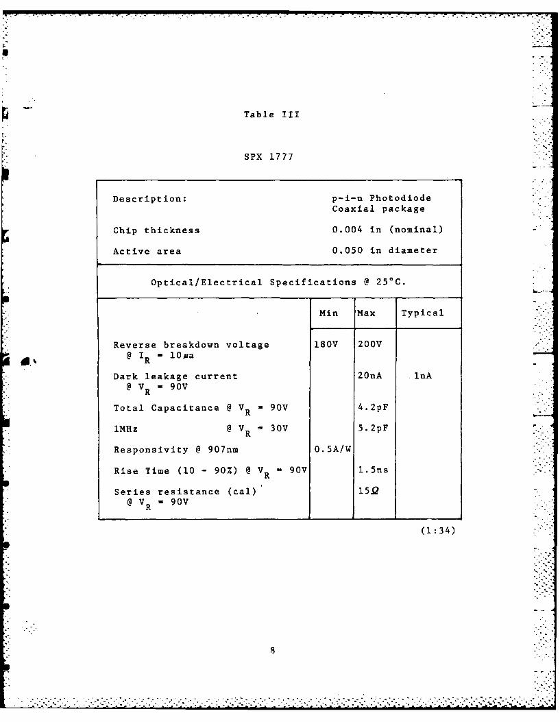
Table III
SPX 1777
Description: p-i-n PhotodiodeCoaxial package
Chip thickness 0.004 in (nominal)
Active area 0.050 in diameter
Optical/Electrical Specifications @ 25*C.
Min Max Typical
Reverse breakdown voltage 180V 200V@ I R= lOpa
Dark leakage current 2OnA lnA@ VR 90V
RR
1MHz @ V R = 30V 5.2pF
Responsivity @907nm 0.5A/W
Rise Time (10 -90%) @ V 90V 1.SnsR
Series resistance (cal)- 15JQ@ V R =90V
(1:34)

Table II
SPX 1775
Description: GaAs Edge Emitting LED
Optical/Electrical Specifications @25*C.
Min Max Typical
Reverse breakdown voltage 4.OV
Forward voltage 1. 5V@ IF = lOma
r 1, 0.Q
CT @ V + 1V, f = MHz 12pfT R
7r. @ lO0ma 907nm
AT @ lO0ma 22nm
Power out 2. 0mW
Q =150 half angle f p 1mW
tr 2Ons
(1:34)
7

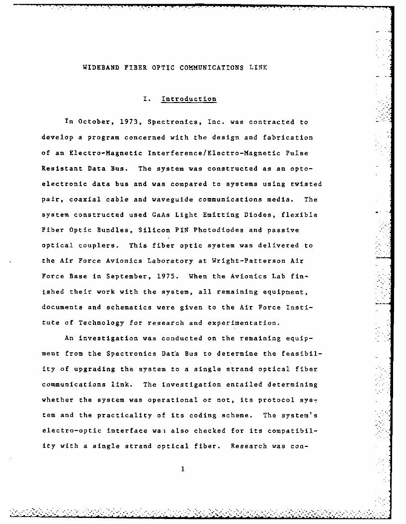
Tables II,III and IV.
__ The Spectronics SPX 1775 LED has an output intensity vs
radius radiation pattern that lends itself very well to use
with optical fiber bundles. As shown in Figure 1, the output
intensity is greatest approximately 17.5 mils distant from
the center axis of the LED. To achieve maximum power trans-
fer into the Valtec fiber bundle the fiber cable was termin-
ated as shown in Figure 2a. For termination into the PD, the
fibers were collected as close to the axial center as possi-
ble, thus putting the maximum amount of optical power on the
active area of the detector. This configuration is shown in ___
Figure 2b.
The Spectronics system seemed ideal for use as an ex-
perimental fiber optic transmission media with some specific,-
inherent limitations. First, the system was designed for use
with fiber optic bundles rather than single strand optical
fiber cable. Recent technology has gone to single fiber be-
cause of improvements in fiber loss characteristics which en-
ables longer transmission lengths with less physical size and
weight, and wider bandwidths at a cost lower than that of the
multi-strand fiber bundles. The Spectronics system of time
division multiplexing made other types of modulation and
multiplexing impractical because of the strict protocol in-
volved with the command and status words. Even if the com-
mand and status word logic could be by-passed, the sync
pulse and parity check assignments in the data words made
S"' this mode of transmission unattractive for more advanced com-

-~7 - . ' *
Communications-Electronics Laboratory at AFIT.
This fiber optic data bus was designed as a lOMbit,
eight user, time division multiplex system with all data
transfers controlled by the CMTU. The MTU's served as the
electronic/fiber uptic interface units for the subsystems or
users.
The system was capable of transferring data from the
controller to the user, user to controller, and from user to
user. Data transfer was accomplished through the use of
three types of words. First, a command word that identified
the terminals involved, transmit/receive, number of data
words to be transmitted, parity check and a synchronous tim-
ing pulse. Second, the status word that contained a sync
pulse, parity check, Subsystem Interface Unit (SSIU) status
bit, parity error bit, terminal identifying address bits and
nine MTU failure code bits. And finally, the data word that
contained a sync pulse, parity check bit and 16 data bits.
The CMTU Test Set was designed as a Bit Error Rate (BER)
Test Set by transmitting the parity error bit from the status
0 word to a detector circuit, then to an external connection
which could be coupled to a standard counter. The number of
bits transmitted was controlled by the length of time the
test was in progress and by knowing the transmission rate.
The optical transmission media was comprised of
Spectronics SPX 1775 Light Emitting Diodes (LED), Spectronics
SPX 1777 p-i-n Photodetectors (PD) and Valtec Fiber Bundles.
Pertinent data for these three components are listed in
5
::7

Table I
EMI/EMP Resistant Data Bus Equipment
Quantity QuantityOriginally Nomenclature RemainingSupplied
7 Multiplex Terminal Unit(MTU)
1 Control Multiplex TerminalUnit (CMTU)
2 MTU Test Set 0
1 CMTU Test Set I
1 1 9 Port Radial Coupler 1
1 Fiber Optics Radial Coupler ICable Assembly
Consisting of 2 each:
10 ft. fiber optic cable20 ft. fiber optic cable30 ft. fiber optic cable50 ft. fiber optic cable
2 Subsystem Interface Unit/MTU 0Interface Cable
1 Controller/CMTU Interface 0
Cable
6 Transit cases 0
3 Power outlet strips 0
(1:5)
4. - -. . . . . . . . . . . . . . . .
. . . . . . . . . . . . . . . . . .
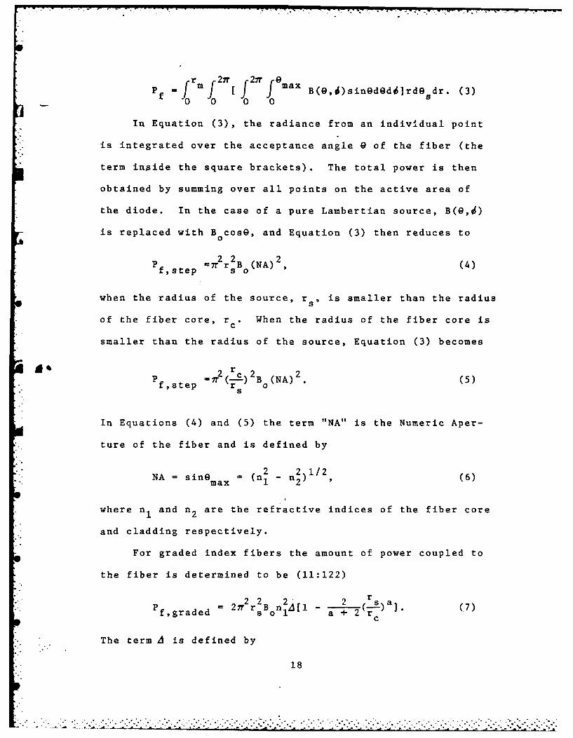
P frm 2 T f2 max B(e,6)sineded4]rde dr. (3)Pf f0 0 0 0
In Equation (3), the radiance from an individual point
is integrated over the acceptance angle e of the fiber (the
term inside the square brackets). The total power is then
obtained by summing over all points on the active area of
the diode. In the case of a pure Lambertian source, B(G,i)
is replaced with Bocose, and Equation (3) then reduces to
Pf-s7 2r 2B (NA) 2 (4)f,step s o
when the radius of the source, rs, is smaller than the radius
of the fiber core, r . When the radius of the fiber core isc
smaller than the radius of the source, Equation (3) becomes
2 r 2 2P 7r (-.) B (NA) . (5)f'step r o' S
In Equations (4) and (5) the term "NA" is the Numeric Aper-
ture of the fiber and is defined by
.• -2 2 1/2NA = sinemax = (n I - n) 2, (6)
where n1 and n 2 are the refractive indices of the fiber core
and cladding respectively.
For graded index fibers the amount of power coupled to
the fiber is determined to be (11:122)
22 2 2 raP 27 r B n 4[l (-) ). (7)f,graded0 1 a + 2 r7c
The term A is defined by
18

l 2 (8)n1
and "a" is the index profile coefficient.
It can be seen from this discussion that the amount of
power coupled to a fiber is primarily a function of the geo-
metry of the source and the fiber, and the fiber's numeric
aperture. Additional losses can occur at the launching point
if the fiber face is misaligned, has high reflectance or if
there is an axial misalignment between the source and fiber.
In the following discussion on fiber to fiber coupling
losses several assumptions are made. Foremost of these
assumptions is that the reader has a good understanding of
electromagnetic mode propagation in a waveguide. The other
assumptions are that all modes propagating in the fiber are
equally excited and the geometries of the fibers and source
are ideal. That is, if the cross section of the fiber is
depicted as circular, then it is treated as a periact circle,
the step change in index of refraction between the fiber
core and cladding is treated as a perfect step and that the
core/cladding interface could be depicted as a smooth sur-
face longitudinally down the fiber.
As an example of fiber to fiber coupling loss, consider
two multi-mode, step index fiber with equal core diameters
joined in a dry connector. The major causes of power loss
in this example are three mechanical misalignments: axial
displacement, longitudinal separation, and angular misalign-
19

ment.
Axial displacement is the most important of the three
misalignments and will be discussed first. If all modes
propagating in the fiber are equally excited, then the per-
centage of power coupled to the receiving fiber is equal to
the common area of the two fiber cores. Figure 6 depicts
this overlapping effect when the axial displacement is equal
2to an amount "d". The area of the fiber core is r and thec
common core area is given by Equation (9).
A 2r2 cos - 1 d 2 - d2 (9)= (2--) - d(r __)l/2. 9
Comm c co 2r c 4c
An inspection of Equation (9) shows that as the dis-
placement approaches twice the magnitude of the core radius
the common area, and therefore the power coupled, goes to
zero.
Axial displacement loss for graded index, or step to
graded index fibers is considerably more involved. The rea-
son for the increased complication is that the controlling
factor at the coupling point is the smaller of the two num-
eric apertures. The changing numeric aperture is a function
of the distance from the fiber axis. Not only is the common
core area integrated but the smaller of the two numeric aper-
tures must be integrated on a point to point basis to deter-
mine the number of modes that can propagate in both fibers.
For a graded index to graded index connection of iden-
tical fibers, with a grading index profile coefficient a
equal to 2, and with the axial displacement much smaller than
20

Common Core Area
Figure 6. Axial Displacement
21

the radius of the core, the power to the receiving fiber can
"" be approximated by (11:134)
P1f,graded -P (1 - 8d (10)
The term Ps in Equation (10) is the total power exiting the
emitting fiber.
Power loss due to longitudinal separation is much less
complicated to calculate, and compared to axial displacement,
causes less loss as the displacement "d" increases. As an
example, consider the two identical step index fibers de-
picted in Figure 7, separated by a longitudinal separation
"d". Again, with all modes equally excited, the percentage
of power coupled to the receiving fiber is equal to the ratio
a. of the c6re area to the area of the expanding beam. The beam
expands at the same angle emax, as the maximum acceptance
angle at the entrance of the fiber. This simple ratio comes
from the assumption of equally excited modes because, since
the fibers are identical, they both support the same number
of modes, and only those modes that reach the receiving
fiber's core face are coupled.
Angular misalignment is mathematically the most compli-
cated of the three mechanical misalignments, but with a small
angular displacement this also accounts for the smallest of
the power losses.
The theoretical loss for two identical step index fibers
with an angular misalignment has been calculated to be
(11:134)
22
............... ..
...... L'_'_. _- -..... _.- ... ' .. '.-.... ... '........ . ......- , ....-.... .. ........ ,,- ..-. -,.

ON
41 -4v-4
0 0
Vc
0
94.
5 0 a
to U,
"4
23-
1 1 p21i/2 1 I'(p
Loss -10log(cos[ -p(l - ) - 1
1 2 1/2 1 -1 1
q(1y[l y + !sin (y) + IM. (11)
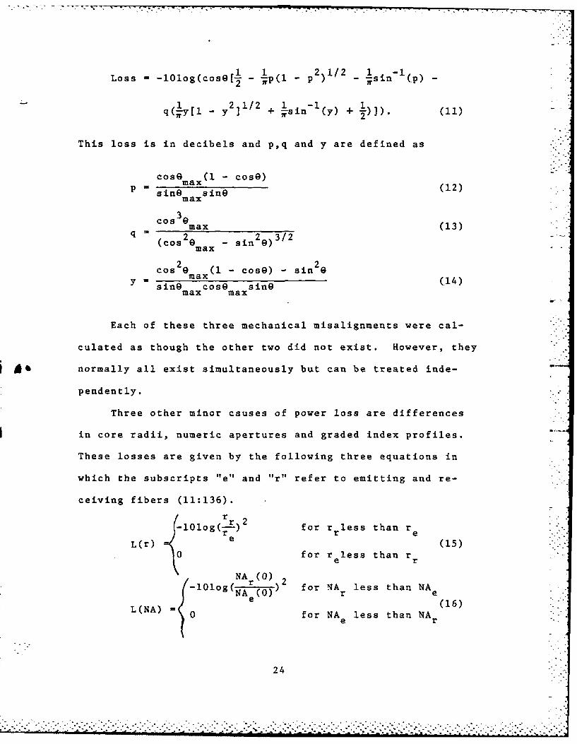
This loss is in decibels and p,q and y are defined as
cose (i - cose)max
sin@ sine (12)max
3cos emax (13)q = 2e - sin 2 )3/2
max
cos 2 8max(1 - cose) - sin2e (14)
sine cose sinemax max
Each of these three mechanical misalignments were cal-
culated as though the other two did not exist. However, they
,, normally all exist simultaneously but can be treated inde-
pendently.
Three other minor causes of power loss are differences
in core radii, numeric apertures and graded index profiles.
These losses are given by the following three equations in
which the subscripts "e" and "r" refer to emitting and re-
ceiving fibers (11:136).
r2lOlog )for r less than rrer eL(r) e (15)
for r less than re r
NA (0)r 2) for NA less than NA
r e(16).
L(NA) =(6 0 =for NA less than NAe r
24
............................................................. '..

a r (a e+ 2)10aOg -) for a less than aae(a r+ 2)) fr ar
L(a) (17)for a less than a
e r
Power loss is not restricted to fiber connections and
source to fiber power launching techniques. The fibers them-
selves have intrinsic losses that can be categorized into
three classes: absorbtion, scattering and radiative losses.
These three types of losses are generally lumped together and
defined as the attenuation coefficient of the fiber and is
measured in decibels per kilometer.
Absorbtion losses are caused by impurities in the glass
of the fiber. Impurities such as iron, cobalt, chromium,
copper and water ions (OH) cause absorbtion by the fiber in
a. the wavelength region of the optical source. The Vapor Phase
Deposition method of fabricating optical fibers creates glass
with impurity counts that are only one percent of those made
by the Direct Melt method (9). Doping the glass with mater-
ials such as germanium-oxide are often used to reduce the ef-
fects of the impurities(16).
Scattering losses arise, from microscopic variations in
material density. Also, since fibers contain oxides like
Silicon-oxide and Germanium-oxide, the index of refraction
varies over distances that are small compared to the wave-
length of the optical power source.
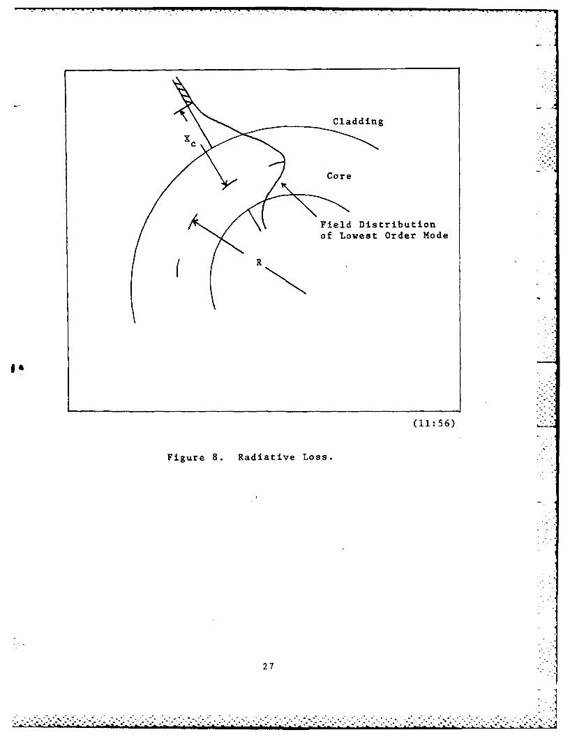
Radiative losses occur whenever there is a bend in the
fiber. Fiber bends occur in two forms; first, when the bend
2....
. -.. -.

radius is much larger that the fiber diameter, and the second
which is due to the microscopic bends or variations at the
core-cladding interface.
The first of these radiative losses is explained with
Figure 8. In this drawing "R" represents the bend radius
and only the lowest order mode propagating is depicted. The
evanescent field in the cladding decays exponentially as a
function of the distance from the core axis. The field tail
moves along with the field in the core; therefore when the
fiber is bent the tail must move faster. At a certain crit-
ical distance x, the tail would have to move faster than
the speed of light to keep up. Since this is impossible, the
field tail radiates away. Higher order modes radiate away
faster because their field tails in the cladding are propor-
tionally larger than the lower order modes. Fiber bends can
be used as fiber optic attenuators or mode controlling filters
because the tighter the fiber is bent the more modes and power
can be radiated away.
Microbends in fibers causing radiative losses are shown
in Figure 9. They can be caused from packaging faults while
jacketing the fiber or from external forces on the fiber ca-
ble. The loss from these microbends is explained in the same
manner as for the larger fiber bends. Microscopic variations
at the core-cladding interface can change the angle of re-
flection within the core and therefore create a mode conver-
sion. If the new mode that was just created cannot be sup-
ported by the fiber then it will radiate away through the
26
Cladding
Core
Field Distributionof Lowest Order Mode
( R
(11:56)
Figure 8. Radiative Loss.
27
- - --- .- -2 ,;.-.-2. ---2 i- i. 2 %- . - 2- i~ -- . .- i--i -- ----- "..- . ~ i i . , .- . .- . . . . .- . .- .- .
FiberJacket
Externaf Force
____ ___ ___ ___ ___ ___Fiber
Jacket
Compressible Filler
(11:57)
Figure 9. Fiber Microbends.
28
cladding and create a power loss.
The major factor that limits the bandwidth of optical
fibers is intermodal distortion. The higher order modes
that propagate in a fiber have lower power content but they
also take longer to traverse the length of the fiber. When
the optical signal reaches the termination of the fiber the
higher order modes, carrying the same information, arrive
later, thus interfering with the lower order modes of sub-
sequent information signals. Obviously, the longer the fiber,
the greater the time spread between the higher and lower or-
der modes and the greater the distortion. Therefore, fibers
that support more modes have greater bandwidth limitations
and the units of this type of distortion is measured in
Hertz per meter.
While surveying for optic fibers to be used on this
system all types of fibers were considered initially. How- . -
ever, single mode fibers were omitted from consideration be-
cause of cost. Table V lists the parameters of four differ-
ent fibers which represents a fair cross section of commer-
cially available fibers and fiber cables.
Emitters., Detectors and Connectors
Emitters, detectors and connectors will be discussed in
most general terms because for the purpose of establishing
this system any optical power source or photodetector with
equivalent electrical characteristics as the SPX 1775 and SPX
1777 could be used as long as they are designed for single
29
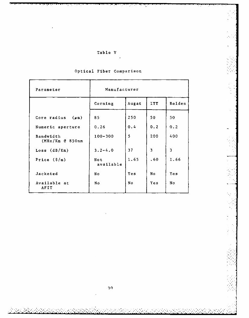
Table V
Optical Fiber Comparison
Parameter Manufacturer
Corning Augat ITT Belden
Core radius (Mum) 85 250 50 50
Numeric aperture 0.26 0.4 0.2 0.2
Bandwidth 100-300 5 200 400(MHz/Km @ 850nm
Loss (dB/Km) 3.2-4.0 37 3 3
Price ($/m) Not 1.65 .60 1.66
available
Jacketed No Yes No Yes
Available at No No Yes NoAFIT

- . .. N
strand fibers instead of multistrand bundles. Connectors
need only be able to couple the fiber to the source or de-
tector with good repeatability in mechanical alignments.
Optical power sources are generally classified into two
categories, Light Emitting Diodes and Laser Diodes. Laser
diodes are normally used for very long communications links
because of their highly directional, higher output power le-
vels and very short time constants. Laser diodes can be mod-
ulated up to the Gigahertz range and higher; however, for
this greatly improved efficiency, their cost is proportion-
ally higher than the more contemporary LED's.
Typical output power levels for LED's are in the micro-
watt to milliwatt range, and rise times of 10 to 50ns. If
a maximum of one third of the pulse duration is allowed for
the rise time, the bandwidth is limited to approximately
3 0MHZ.
Light Emitting Diodes normally come in one of two stan-
dard packages known as surface emitters or edge emitters.
Surface emitting LED's are permanently connected to a fiber
with an epoxied butt joint right to the active surface of the
diode. Edge emitting diodes have internal reflecting plates
that direct the output optical power parallel to the active
area creating a directionalized radiance pattern. This al-
lows more power to be coupled to a fiber that is not butted
directly against the diode's surface.
Surface emitting LED's come with a pigtail fiber perma-
nently attached to the diode and the communications fiber
31
. . .°.

Table VIII
Equipment Required
Description Quantity
LED 4
PD 4
Panel mount BNC mating connector 12
SMA Fiber terminating connector 2
DPDT Switch 12
Front panel 4
Optical fiber AsNeeded
Table IX
Support Equipment Required
Soldering iron and solder Optical power meter
Wire wrap tool HeNe Laser
Signal generator Fiber holding fixture
Oscilloscope Fiber termination kit
45

terminated with a standard SMA style connector can be tested
with this system. Since one CMTU and three MTU's are avail-
able, four such systems could be constructed.
System operations tests will consist of a complete func-
tional check, and an LED emission pattern characterization. " -
Also, when the fiber to be used is terminated with a con-
nector it will be tested for proper termination, numeric
aperture and fiber attenuation.
An Operations Manual will be prepared for the complete
system. The manual will contain a functional description of
the system and its subsystems, instructions for front panel
operation and schematics of all components in use within the
units.
Material Required
Table VIII lists the equipment '-'at has been procured,
either locally (in-house), or commercially purchased, to
complete this work.
.Support Equipment
Table IX lists the support equipment required.
Additional Support Required
The only additional support required is a minimal amount
of machine shop support in making new front panels for the
CMTU and MTU cabinets.
44
..............................................
................................................ .. ..i.i....: . :[.'-'..i. -".".".-...--'.-,-.--',--..- ......-.. ".-
Carrier modulation is possible on an internally generated
20MHz clock signal or on an externally provided carrier sig-
nal.
- The CMTU and MTU's received from Spectronics are very
similar in design and construction. The difference in the
units lies in their control logic circuits and their inter-
face with their test sets. Because of their similarities,
their changes are identical and are as follows.
•* Have new front panel made.
•* Mount new LED, PD, BNC connectors and function
control switches.
•* Remove internal control circuitry and cross con-
nect wiring.
•* Design, construct and install new control circuit
that will implement the selected functions of baseband trans-
mission or carrier modulation. Install new cross connect
wiring for front panel controls and data lines to and from
the LED driver card and post detector amplifier.
As a result of these changes the system is now a sim-
plex, single strand, fiber optics communications system cap-
able of transmitting both digital baseband and carrier modu-
lated signals. The system is self contained with both the
transmitting LED and receiving PD housed in the same cabinet.
The system is compatible with any TTL, digital modulating
system for creating PCM, PPM, PDM or quantized PAM baseband
signals. The fiber link in use during test is looped from
the LED to the PD on the unit in test. Any optical fiber
43
. . . .. ,..~... .

Table VII
Augat 698-069DG1
Description: p-i-n Photodiode
Coaxial package
Active area 0.105 X 0.043 in.
Optical/Electrical Specifications @25*C,V =5.0Vc c
Min Max Typical
Reverse voltage 10 0V
Dark leakage current 20na@ V 2850Vbias
bCapacitance lp@Vbias 5
Responsivity 0. 53A/W@ 880nm
Response timne 3. 8ns@ bias 50
N.E.P. 10l3W/Hzl/@ V bia 5y, @ KHz
(20)
42

Table VI
Augat 698-013EG2
Description: Edge Emitting LED
Optical/Electrical Specifications @ 25C andV =5.OVcc
Min Max Typical
Reverse breakdown voltage 3.OV
Forward voltage 1.9V 1.75V@ IF = lOOma
7, 880nm
40nm
Power output 38PW
Optical rise and fall time 20ns
(20)
41
is not being used.
- The Spectronics SPX 1775 LED is being removed for
two reasons. First, it was initially designed for use with
multistrand bundles as evidenced by the description of its
emission pattern in Chapter 2. Second, the connecting brack-
et manufactured by Cannon Electric Division is not suited
for a simplex system where frequent changing of the optical
fiber is expected. This original bracket, which houses both
the LED and the PD, is being swapped out for a more conven-
tional SMA coupling mount. The LED selected as the replace-
ment is the Augat 698-013EG2. The pertinent optical and
electrical specifications are listed in Table VI. This LED
is bulkhead mountable and has equivalent characteristics as
the SPX 1775.
- The Spectronics SPX 1777 PD is being removed because
of its mounting bracket and its suspected age. The detector
is being replaced with an Augat 698-069DG1. This new detec-
tor is also bulkhead mountable with an SMA style mating con-
nection. Specifications for this detector are listed in
Table VII. A quick comparison with the information listed
for the SPX 1777 shows that they are equivalent.
- The CMTU Test Set from the data bus package is not
being used because of its inherent dependency on control
logic with the CMTU. The system that has been designed is
very basic, and is composed of an optical transmitter and
receiver housed in the same cabinet, and the fiber link. In-
puts are available for transmitting digital baseband signals.
40 4 0 +i-1 ,
.......................... . . ... .'.

Lastly, an Operations Manual was prepared to facilitate
future use of the system.
Approach
The most effective use of the available equipment was
the primary concern throughout this work. The Spectronics
EMI/EMP Resistant Data Bus has been determined to be capable
of supporting a single strand fiber optics communications
system with several modifications. The changes and the rea-
sons for these changes are as follows.
- The Valtec multi-strand fiber cables needed to be re-
placed with single strand optical fiber. The ITT fiber that
was already available was terminated with standard SMA style
connectors as described in Chapter 2. Because the fiber was
not jacketed, there was a slight modification to the termina-
tion. The crimp sleeve which would normally be clamped to
the jacket was omitted. The rest of the termination procedure
of epoxying and lapping the face of the connector and fiber
was completed as per manufacturer's directions. The connector
selected for use was the Optical Fiber Technologies, Inc., . -
part number 252-S-A. This connector is suitable for fibers
with core diameters less than 125#m and has a connection
loss of less than 2dB.
- This optical fiber system is initially being designed
as a simplex system with information flowing in one direction
from a single transmitter to a single receiver. Therefore,
the radial coupler that accompanied the Spectronics Data Bus
39

III. Problem Statement and Approach
This chapter contains the exact problem statement of
this work, its scope, the approach to the problem and lists
the material and equipment required to complete the task.
Problem
Design and implement a single strand fiber optics com-
munications system to be used by AFIT faculty and students
for future c-ommunications experiments *and research.
Scope
The bulk of the background investigation for this work
was done in the area of optical fibers and their use as a
communications media. Secondary to this was research into
optical sources, photodetectors, optical fiber connectors
and couplers, with emphasis on their applicability towards
this work.
A survey of both on-hand equipment and commercially
available equipment was conducted to determine the most ef-
fective use of resources.
In-house available equipment deemed necessary was then
assembled along with commercially purchased items to con-
struct the system. Once the modifications on existing equip-
ment and construction of new components were completed, oper-
ational tests on the equipment were performed. Operational
tests were done at both the component and the system level.
38

If a ray enters the fiber at some angle e, is trapped and
propagates down the fiber it maintains the same angle with
respect to the core axis until it reaches the other end of
the fiber. Therefore, when the ray exits the fiber, it does
so at the same angle at which it entered. The angle of the
expanding exit beam is the same as that of the light ray
that was accepted at the entrance to the fiber, and this is
the numeric aperture.
The last test is that of determining the attenuation of
the fiber. This is the simplest of the four where the fiber
is connected to an optical power source and a power reading
is taken from the other end of the fiber with an optical
power meter; Then the fiber is shortened and another power
reading is taken. The difference in power readings divided
by the length that the fiber was shortened yields the fiber's
attenuation constant in units of decibels per meter.
For a fiber optic communications system without splices
or fiber to fiber connections these four tests give suffi-
cient information to perform power budget calculations for
the optics medium. When the responsivity of the photode-
tector is known along with the output power of the LED, it
can be determined if enough power will be coupled to the fi-
ber and whether the fiber will attenuate the optical signal
beyond the capabilities of the detector.
37
.1-. ,..•...... ............ ... ,.......... . .•."]
used to determine if the optical source is suitable for the
desired purpose.
Fiber termination characterization is really just a sim-
ple check to see how well the fiber face has been prepared.
The terminated fiber end under test is attached to a compati-
ble optical source with the other end of the fiber connected
to an optical power meter. An initial reading is recorded;
then the fiber is rotated 900 three times with readings re-
corded at each of the positions. A comparison of the read-
ings will give an indication of whether the face of the fi-
ber has been finished flat and normal to the axis of the fi-
ber.
The optical power source normally used to measure the
numeric aperture (NA) of a fiber is a low powered laser in-
stead of an LED. The laser beam is focused on the end of
the fiber and the other end of the fiber is aimed at a screen
located a convenient distance away. A simple measurement of
the beam image on the screen is taken, and knowing the dis-
tance of the screen from the fiber end the beam angle can be
calculated by taking the arctangent of the beam width on the
screen divided by twice the distance from the fiber end to
the screen. A fiber's numeric aperture is a measure of its
light collecting ability and is defined as the sine of the
maximum angle that light can enter the fiber's face and be
trapped by internal reflections inside the fiber's core.
This test is a valid method of determining a fiber's NA and
can easily be proven by using simple geometric ray optics.
36
Ii:- .i. i ., i :: :.i.:.:. ij i:: -:: -:-: -. .- , .. i.:.. :- . ... -i°••:....... .i.-.:.i. .:, . . .. i, .. ,ii!

- ~ ~ ~ ~ ~ ~ o e Supply ' -s-- - . -- - -. . . . . .
OOptical Fiber
Figure 11. Setup for Meastiring LED Emission Pattern.
35

fr V-1.170" Typ.
Assembled View
(7)
Figure 10. Optical Fiber Technologies, Inc.,200-S Styled SMA Connector.
34

Figure 10. These connectors are moderately priced and read-
"" ily abailable in sizes to fit standard fiber core diameters.
These SMA connectors are of the concentric-sleeve type
as opposed to the tapered sleeve or V-groove types. Also,
they have no lens systems for beam expansion nor index
matching fluid to increase coupling efficiency. They are
simple dry joint butt connectors.
Experimental Measurements of the Optical System
There are four very basic measurements that can be per-
formed on an optical fiber communications system that yield
somewhat of an overall characterization of the optical link.
These tests are: optical source output radiation pattern,
fiber termination characteristics, numeric aperture of the
fiber and fiber attenuation. A general description of these
tests will be presented in this section.
To determine the emission pattern of the optical source,
the source must first be firmly fixed in a position which al-
lows access to the output energy from all directions. Such a
position is depicted in Figure 11. A short piece of optical
fiber will serve as a light collecting instrument which is
connected to an optical power meter. The relative power
readings are recorded as the fiber is moved around a hemi-
spherical surface insuring that the polished face of the fi-
ber always remains normal to the light source. The power
measurements can then be plotted and a diagram of the output
emission pattern is obtained. This information can then be
33

must then be spliced or in some way connected to the pigtail.
This method may be adequate for fixed communications links,
but the edge emitting LED is more suited for a system where
the fiber link might be disconnected and reassembled many
times. Edge emitting LED's are available packaged in bracket
or bulkhead mountings complete with microlens systems for
additional focusing of the optical power allowing better
coupling efficiency to the fiber.
Photodiodes use the photoelectric effect of semiconduc-
tors to convert optical power to electrical current. The
p-i-n PD is used as a simple photon counter which outputs a
current proportional to the number of photons impinging on
its active surface area. The avalanche photodiode is similar
in that its active surface area creates an electron flow when
photons strike, but as the electrons propagate through the
semiconductor they cause additional electrons to move giving
the device a relative gain in output current. The avalanche
PD's are used when there are low input optical power levels
requiring a more sensitive optical receiver.
Photodetectors used in fiber optic communications sys-
tems are available packaged in all the standard mountings
with standard fiber coupling connectors.
Optical fiber connections range from arc fusion welding
of the glass to temporary plastic clip-on connectors. By far
the most common type connector for a reliable, removeable
connection is the standard SMA styled metal screw-on fiber
connector. An example of this type of connector is shown in
32
p' i;m- , ' , '. . , - - ;. , ... -_. . -
IV. System Implementation
The eight station, Spectronics EMI/EMP Resistant Data
Bus was converted to a two piece, single strand optical fi-
ber communications system after the changes described in the
third section of Chapter III. The changes were accomplished
in four phases. Chronologically, the CMTU and MTU cabinets
were stripped of wiring and components not needed in the new
system. A new controlling circuit was designed and built to
accomodate the functions of the new system. The cabinets
were modified to properly house the new components, connect-
ors and switches. And finally, the components were installed
on the modified cabinet and the test fiber was terminated
with new connectors. Details of each of these four phases
are presented in the following four sections.
Component Removal
It was determined that five of the nine circuit cards in
the CMTU and MTU would be used in the new system. These five
were circuit cards A5 through A9, namely the ECL/TTL Convertor,
ECL Sync Detector, LED Driver, Preamp and Postamp Signal Con-
ditioning cards. The last three of these cards listed above
were kept to provide the TTL interface to the LED and PD. The
ECL Sync Detector also generates the system clock signals of
100MHz, 20MHz and 4MHz. The ECL/TTL Convertor card was kept
to provide TTL compatible clock signals that could be used
as digital carrier signals for the system.
46
-- - a. a a.a . .

The remaining four cards were not discarded entirely.
The A4 card was stripped of all wiring and components to be
used for the new controlling circuit. The integrated cir-
cuit chips on the cards Al through A4 were then available for
use in this new circuit. All cross connect wiring was re-
moved from the card sockets and front panel. However, the
power supply and serial data stream lines were left intact.
The LED and PD connector was removed and then it was
determined that the front panel should be replaced because
of the numerous holes that would remain unused with the new
system.
Control Circuit Design and Construction
The control circuit that was designed was done so to
properly handle the functions described in Chapter 3. On
the transmit side, either baseband or externally modulated
carrier TTL signals were coupled directly to the LED driver
circuit. Also when so desired, the input baseband signal
modulated either the internal 20MHz carrier or an externally
provided carrier. On the receive side, the circuit had to
do the inverse of the transmit. Namely, it had to couple a
baseband signal directly to the output, or if carrier modu-
lation was used then it had to regenerate the original base-
band signal.
Figure 12 is a logic diagram of the circuit designed.
In this figure the symbols are as follows: Sl, S2 and S3
are controlling switches, BBI is baseband input, BBO is the
47
. . .. .. .. ........ .
. . . . . . . . . . . . .. . . . . . . . . . . . . . . . . . . . . . . . . .
f "."-i . F --. .i ,"-, .,-.,- ,.'.-'.-., ... ,'.,'..'.,- % .- -i .,' -" -'.---.,-.'-',-.-",'...-'.-.-.-.' .•. . :..-. -i""i'.. '"-i.-..-.*.*.*---%'-*.

DFR DTX
INTC
EXTC
S3
Figure 12. Logic Diagram of Control Circuit.
48
baseband output, DFR is data from the receiver, DTX is data
to transmitter, and INTC and EXTC are the internal and ex-
ternal carriers respectively.
When S1 is low, BBI and DFR are connected to DTX and BBO
simultaneously. This state constitutes baseband transmission
mode only. When S1 is high, the carrier signal selected by
S3 is AND'd with BBI creating the carrier modulated signal to
DTX. Also, when S1 is high, the received modulated signal,
DFR, is the input to a D flip-flop which is clocked by either
the carrier or the inverted carrier (selected by S2). The D
flip-flop is triggered by the positive going transition of the
of the carrier frequency and therefore remains high through
the entire period of the carrier signal. This function de-
modulates the signal back to baseband and S2 performs the
function of a synchronizer. There is no actual synchroniza-
tion performed here but when the same carrier frequency is
used for both the transmit and receive the transmission delay
could cause the signal to be sampled during the low state of
the received carrier modulated signal. If this occurs then
the output to BBO will always remain low. When this happens,
changing the sense of S2 effectively causes a 1800 shift in
the carrier triggering signal resulting in proper samplingtiming.
This circuit was assembled on the empty A4 card using
standard wire wrap techniques. The wiring diagram for this
circuit is given in Figure 13. After its construction, the
circuit was tested and all functions operated as designed.
49

E-4 N?
CM,
C14,
1-4-
040
'-44
4-1-
-r4 0 -
ci-9 %: 4-4)c c *
m P-4-4 P2>9-C
0'-
0 E-4
U4Z
C14
r-4 -4 00>4 -4, PQ>45 r
v - r -4.. - f C . 0 4 c a -

Cabinet Modifications
Changes in the cabinets of the CMTU and MTU were very
similar. The only difference was that with the MTU three . -
BNC connectors were removed from the rear panel to be in-
stalled on the front. The two common changes were the de-
sign and acquisition of a new front panel and removal of an
alignment flange.
The RFI enclosure for the LED driver, preamp and signal
conditioning cards had an alignment flange for the LED and PD
mounting bracket. The flange protruded through the front
panel to the bracket and ensured proper alignment of the LED
and PD to the driver and preamp for a direct connection.
This flange was removed entirely but the RFI enclosure was
retained as a circuit board mount for the three cards within.
The front panels that came with the original equipment
could have served with the new system with all the existing
holes covered with small plates. This, however, would have
necessitated moving the RFI enclosure and making new holes
for the new LED and PD. Also, the front panel was etched
and painted describing the function of the connectors and
switches. Since all connectors were to serve new functions
and more switches were to be added, the panel labeling would
have been misleading. Therefore, a new panel was designed
and ordered through the machine shop. The original schematic
for the front panel was used as a guide and a description of
the new panel is given in Figure 14.
51
-I"°

Note: All dimensions in inches.
~j+- j -1- 1 -i'--- Z -. r--..- -o
,D'o. DD
_~t, PiCs. Pic$. @
/DIG
3If
Material: 1/10" Thick Aluminum Alloy
Figure 14. Diagram of New Front Panel.
52
............ ................. i -i"*'"" "" "': .'" - :" "-"-.- -" ":.''v '.,.."" '.,.. .'.. ".,'.....''..... . . ..... .'.... . ... '.....:'..'''..:..

Component Installation and Fiber Terminations
When the Augat LED's and PD's were received, they were
installed and soldered to the driver and post detection amp-
lifier cards with only one minor problem. The mounting
holes bored in the new front cover were aligned with the
positions of the old LED and PD, and the resulting dimen-
sions did not allow room for the lockinag nuts or the hex nut
locking clamp for the fiber connectors. Therefore, the two
mounting holes were filed out to make a rectangular opening
large enough to accomodate the new components and a small
cover plate with properly aligned mounting holes was made to
hold the LED and PD. This solution has proven to be quite
adequate.
In the Spectronics Technical Report on the EMI/EMP Re-
sistant Data Bus, much effort was dedicated to the descrip-
tion and design of the post detection amplifier and signal
conditioning circuit cards. Primary in their concerns was
the upper cutoff frequency of these components in conjunction
with the photodetector. In their analysis, the upper limit
for the system rise time was determined to be 35 nsec. Leav-
ing approximately the same time period for the fall time,
the system bit rate was thus limited to 12.5 MHz. Because of
a delay in receiving the LED and PD for this work, ample time
was available to investigate these frequency limitations.
To simulate the completed system equivalent LED's and PD's
were connected to the system via long wires and mounted on a
53
S..i". .' .' , .. -' ," " ,/. . .',' . ,. .' .' . .'.' , ,:.' . ,' . , '," , ,. '.-. '.-. ' .' ,. '. ' -,-. . . .. '-'-.- . . . ." .

temporary mounting board. This was necessary because the
components were not of the SMA compatible, bulkhead mounting
types. This did, however, allow very convenient test points
for monitoring circuit response. It was noted that as the
frequency of the transmitted signal was increased the output
of the postdetection amplifier went from a near perfect
square wave to a triangular waveshape of changing slope near-
ly proportional to the input frequency. The slope of this
signal approached zero as the frequency reached 10.5 MHz.
More importantly, however, was the fact that the average le-
vel of this triangular waveshape varied with input optical
power levels. This directly effected the frequency limita-
tions of the system. If the optical power was great enough,
the signal never fell below the threshold of the post detec-
tion amplifier and the system output remained high. If the
optical power was too low then the peak of the triangular
wave never exceeded the threshold and the output remained -
low. At lower frequencies, below 1 MHz, this effect was
negligible. No optical power measurements were taken at
this time because of the impending LED, PD and optical fiber
changes.
All tools and materials required to attach the stainless
steel OFTI, SMA styled fiber connectors were located in the
new Engineering Optics Lab located in building 194, Area B,
of Wright-Patterson AFB. Using an optical fiber stripping
tool, enough of the plastic coating was removed from the ITT
fiber to allow just the core and cladding to extend approxi-
94
mately a quarter of an inch through the alignment hole of
the connector. Epoxy was then mixed and applied to the fi-
ber and connector. To insure adequate adhesion, the back of
the connector was filled with epoxy along with a small bead
of epoxy on the connector's face. The fiber was moved in
and out of the connector a few times to allow the epoxy to
completely fill the fiber alignment cylinder. The epoxy was
cured with a heat gun for approximately ten minutes, until
the epoxy turned a very dark red, and then the excess fiber
protruding through the epoxy bead on the face of the connec-
tor was broken off. The excess epoxy and fiber on the face
of the connector was removed with a coarse lapping film and
the connector's face and fiber end was then polished flat
with finer grades of lapping film. This procedure was used
on both ends of the optical fiber and continuity was checked
by placing one end of the fiber in front of an incandescent
light bulb and checking the other end of the fiber under a
microscope. No problems were encountered while making this
two meter piece of test fiber.
55
. .. . .. "

V. Fiber Testing and System Operation
The testing done on the completed system as described
in the previous chapters can be broken down into three cate-
gories. First, the fiber itself was tested for Numeric Aper-
ture, attenuation, and connector loss. Next, the LED was
energized and its emission radiation pattern was character-
ized. And last, the system was tested for both its modula-
tion capabilities and frequency response. The following is
a description of the tests and their results in the order
presented above.
Fiber Tests
Numeric Aperture, The test performed to measure the
fiber's numeric aperture (NA) was both the most involved
and the most interesting of the three tests done on the fiber.
The NA test was performed on the fiber before the OFTI con-
nectors were installed on the ends. This procedure, without
connectors, necessitated that the fiber ends be cleaved to
obtain a flat face perpindicular to the fiber axis. The
XYZ positioning clamp to hold the fiber at the focal point
of the laser light also required that about three inches of
the plastic coating be removed. This was quite difficult
because the fragile glass fiber inside broke repeatedly,
Table X lists the equipment required for this test.
56
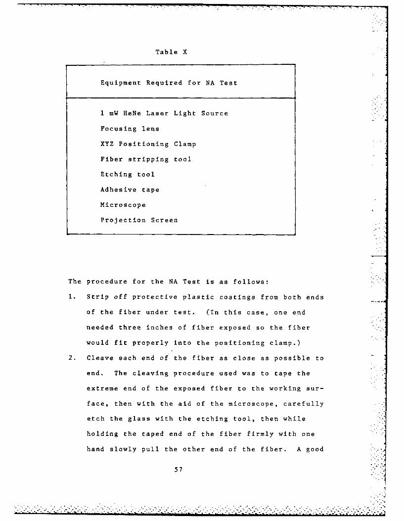
Table X
Equipment Required for NA Test
1 mW HeNe Laser Light Source
Focusing lens
XYZ Positioning Clamp
Fiber stripping tool
Etching tool
Adhesive tape
Microscope
Projection Screen
The procedure for the NA Test is as follows:
1. Strip off protective plastic coatings from both ends
of the fiber under test. (In this case, one end
needed three inches of fiber exposed so the fiber
would fit properly into the positioning clamp.)
2. Cleave each end of the fiber as close as possible to
end. The cleaving procedure used was to tape the
extreme end of the exposed fiber to the working sur-
face, then with the aid of the microscope, carefully
etch the glass with the etching tool, then while
holding the taped end of the fiber firmly with one
hand slowly pull the other end of the fiber. A good
57
%% 1
m .+ +- ". .. .' -m . . . . . . . . . . . . ..'lm im I ~ mlm .. .. . ... " . . . .. . . ....

cleave is achieved when the fiber breaks at the
point of the etch mark. The fiber end should now
be completely flat and perpendicular to the fiber
axis.
3. Place the fiber so that one end is in the XYZ Clamp
and the other is fixed in a position normal to and
a convenient distance away from the projection
screen. (In this case a piece of clean white paper
was used as the screen.)
4. Turn on the laser light source, and with the XYZ
Positioning Clamp, move the cleaved fiber end to
the focal point of the lens in front of the laser.
(When the fiber end is at the focal point, the op-
tical power exiting the other end is at a maximum.)
5. Measure the diameter of the circle of light on the
screen, "d", then measure the distance from the fi- -
ber end to the screen "1".
The data from these two measurements are then used in
the equation NA = sin[tan (d/21)] to determine the fiber's
numeric aperture.
When this test was performed on the ITT fiber, the dia-
meter of the light circle was 4.5 inches, and the distance
from the screen to the fiber end was 12 inches. These measure-
ments resulted in a calculated NA of 0.184 which correlates
very well with the stated NA of 0.19 from the manufacturer.
One very important property of optical fibers must be
kept in mind before performing this test. When light is
58 •
I&.

initially launched into a fiber, many modes will propagate
for a short distance before th-e higher order modes radiate
away through the cladding. Therefore, to measure the "equi-
librium NA" versus the "insertion NA", a piece of fiber in
excess of 10 meters in length should be used or some other
type of mode stripping would have to be accomplished. One
common form of mode stripping is to remove any protective
coverings from the fiber and directly expose the core, if
possible. Then, while bending the fiber at the exposed sec-
tion, cover the glass with an index matching liquid like gly-
cerin. The number of modes that can be removed utilizing
this technique is directly dependent on the radius of curva-
ture at the bend, and the index of refraction and purity of
the index matching fluid.
In the case of this work, the length of fiber used for
this NA test was approximately 100 meters. Therefore, the
0.184 NA calculated is assumed to be the equilibrium NA.
Other noteworthy observations resulting from this test
involve the shapes of the light images on the screen while
trying to get a good cleave on the fiber end. In particular,
there were three different times that it was thought that
there was a good cleave on the end of the fiber, but the
image on the screen was not even close to the expected per-
fect circle.
A good cleave was achieved on one end and was installed
in the XYZ clamp. The other end was cleaved and under the
microscope it appeared to be a good finish. However, while
59

the baseband signal only.
The last test performed on this single strand fiber-op-
tic communications system was that of average optical power
output versus frequency. The results of this test should be
helpful when system optical power budget calculations are
made. The Photodyne Optical Power Meter was used with the
fiber constructed for this work to record the power levels.
The measured fiber loss of 9.4 dBm was added to each reading
to give the actual power output of the LED at each fre-ncy.
Figure 17 is a plot of the results of this test. It Wo
noted that at 22 Mbit/sec there was a rise in power of 0.5
dBm and this was also the cutoff frequency for the photode-
tector conditioning circuit. Therefore, it was presumed
that this optical power level of 2.3 dBm was also the upper
threshold of the receiving circuitry.
The output power was also checked at dc, and a level of
2.8 dBm was observed. This is identical to the power level
transmitted at frequencies above 32 Mbit/sec which confirms
that the LED remains on constantly above this upper bound.
73
. -. .- .
electro-optic interface. When the signal from the LED driver
was checked it was observed that at 32 Mbit/sec the driver
output remained high constantly. Additionally, when the out-
put of the post detection amplifier was monitored it was ob-
served that the signal level remained sufficiently high
enough to stay above threshold at rates higher than 22 Mbit/
sec. Hence this 22 Mbit/sec upper bound was real and deter-
mined to be the result of the relatively slow time constant
of the circuit comprised of the PD, post detection amplifier,
and signal conditioning cards. At this point it was also de-
termined that the internal 20 MHz (40 Mbit/sec) carrier could
not have been transmitted as believed in previous tests.
When the carrier signal was modulated by the baseband, it
merely kept the LED activated until the baseband signal re-
turned to the low state and therefore the a'ctual signal being
transmitted optically was identical to the baseband only in-
put.
For the externally provided carrier mode the carrier
frequencies enjoyed the same range as the baseband mode. Car-
rier frequencies from 160 Kbit/sec to 20 Mbit/sec were used
on a range of baseband signais from 80 Kbitisec to 10 Mbit/sec.
It was noted that in this mode the limitations were caused by
and responded identically to those in the baseband mode.
That is, when baseband signals below 80 Kbit/sec were used,
regardless of the external carrier frequency, the duty period .. "
of the square wave dropped below 40%. An if the carrier fre-
quency was set above 22 Mbit/sec the optical signal followed
72
was actually taking place. To test for proper operation, the
external carrier modulation mode was used but with the speeds
of the baseband and carrier reversed. In this configuration
it was very evident that the baseband of 2 Mbit/sec was being
turned on and off at the carrier rate of 200 Kbit/sec and op-
erating as designed. Without a hardware change it was impos-
sible to perform the same test using the internally provided
carrier. Up to this point it was thought that the internal
carrier mode also functioned as designed.
Next, the range of the system was tested. Initially, it
was checked only in the baseband mode starting with a bit rate
of 200 Kbit/sec. While dropping the bit rates, at 80 Kbit/sec
there started a noticeable change in the duty period of the
square wave at the output. At this bit rate the duty period
had dropped to about 40% instead of the expected 50%. By the
time the bit rate was dropped to 40 Kbit/sec the duty period
had dropped an additional 30%. Therefore, it was deemed that
the low end of the input range on the system was 80 Kbit/sec.
On the high end a usable signal was still present at 22 Mbit/
sec. However, the output of the function generator at this
speed had noticeable roll-off and ringing, because of this
imperfect input signal and it was impossible to determine if
the system could reliably operate at higher speeds. Since
the system did operate well up to this speed the input band-
with was limited from 80 Kbit/sec to 20 Mbit/sec.
This upper bound of 20 Mbit/sec was investigated further
by removing the front panel to check signal levels at the
71
................................................. .•.................................

input baseband frequency of 100 KHz.
The system functional tests consisted of transmitting four
types of signals across the optical path. The four types were;
straight baseband, externally modulated baseband, and inter-
nally modulated signals using both the internal 20 MHz carrier
and an externally provided carrier. Two Wave-Tech function
generators provided the signals for both the baseband and ex-
ternal carrier. A dual trace Hewlett-Packard oscilloscope was
used as the receiving equipment. The oscilloscope's fastest
scan time was 25 nsec/div with a grid size of 10 divisions and
was adequate for displaying signals up to 20 MHz. The func-
tion generators had both variably attenuated outputs with a
choice of waveshapes and a TTL compatible synchronous pulse
output. The TTL outputs became considerably distorted past
the speed of about 2 MHz and therefore, the waveshape function
outputs were used exclusively during testing. This choice
brought about a nuisance problem in that this output was not
linear and every time the output frequency was changed the
amplitude and dc offset of the signal had to be adjusted.
System functional tests were completed in two stages.
First, all four functions were checked with a continuous bit
stream at the rate of 200 Kbit/sec for the baseband and an ex-
ternal carrier continuous bit stream of 2 Mbit/sec. Then the
speed ranges of the four functions were determined.
All four functions performed as expected. However, since
the system only outputs a baseband signal when it is in the
carrier mode it was impossible to see if the modulation
70
o-
• . . % -
.. .. . . _ _ . . , ' - | .. , . , . . • • . , . . . -, - -
the Full Width Half Max angle of this LED was about 6*, or
from -3 to +3*. This result confirms the high directional-
ity of the edge emitting LED. However, it must be kept in
mind that the LED comes housed in a SMA compatible mounting
and the actual emission source is recessed 3/8 inches inside -
the mounting and this effects the radiation pattern at dis-
tance greater than this.
System Operational Tests
Operational testing was rather limited for the optical
communications system constructed in this work. It was lim-
ited inasmuch as signal to noise and bit error rate tests
were not performed. Functional tests for both baseband and
carrier modulation as well as average output optical power
versus frequency of baseband input were performed.
Before the functional and frequency response tests were
performed, an attempt was made to determine the absolute loss
of the fiber constructed for this project. The Photodyne
Optical Power Meter was first placed directly in front of the
SMA mounting of the LED and a reading of 0.4 dBm was recorded;
then the fiber with connectors attached was placed between
the LED and the power meter and a reading of -9.0 dBm was ob-
served. This 9.4 dBm, or 88.5%, power loss was the absolute
loss of the fiber media, however, it was impossible to deter-
mine how much loss could be contributed to the fiber charac-
teristics or the connections themselves. This test was con-
ducted on the system in its completed configuration with an
69
............... . . . . . . . . . . . . . . . . . . . . .'' ' *. . . . . . . . . .

-- 300
LED-Surface Area
-10
-~ +150
.+00
+30
-30 -20 -10 0
dBm
Figure 16. LED Emission Radiation Pattern.
68

connector placed on and parallel to the grid, the light col-
lector would remain in the same plane as the emission angle
was swept. Since this test was one of relative measurements,
one main concern was to keep the light collector the same
distance from the source and the actual distance between the
collector and source was insignificant as long as the opti-
cal power was within the range of the meter. A distance of
approximately three inches was used for this test. The data
collected from this test is listed in Table XII.
Table XII
Emission Radiation Pattern
Angle from LED Axis Relative Power Reading
-150 -29 dBm
-100 -19 dBm
-50 -9 dBm
00 0 dBm
+50 -9 dBm
+100 -19 dBm
+150 -29 dBm
The plot of this radiation pattern is shown in Figure
16. From this data one could extrapolate to determine that
67
. . -. . . . - .
in this type of test it is impossible to determine if the
loss was caused by axial displacement or angular misalign-
ment. Also, there are uncontrollable nonlinearities in the
connector, LED, power meter. That is to say that even though
the locking clamp of the connector was not moved there does
exist some limited amount of play in the connector and this
may be the cause of the axial displacement loss rather than
the positioning of the fiber concentrically within the align-
ment cylinder.
Because of the nature of this work these results are
relatively insignificant. However, when the power budget
formulas for an optical power link are solved the difference
in positioning of the fiber connectors may become a very sig-
nificant factor. This test allows the designer of a system
to know the range of the controllable factors he has to work
with.
LED Emission Radiation Pattern
The emission radiation pattern of the Augat 698-013EG2
LED was determined after it was installed in the cabinet that
was remodeled for this work. For this test the cabinet
served as the stable holding fixture. The Photodyne power
meter was used as the measuring device. The light collector
used was the optic fiber with SMA connectors at both ends
that was discussed in section II of this chapter. The test
setup was very similar to that of Figure 11. A grid with
angle markings was made and placed such that with the fiber
66
7 •
............................................... . ... .... .... .... ...

connectors installed and the power meter was the same Photo-
dyne Model IIXE. The optical source was the optical commun- • .
ications system constructed with the Augat LED. Optical po-
wer readings were taken at every 90* of rotation and the test
repeated five times for each end of the fiber. The results
were consistent and are listed in Table XI.
Table XI
Connector Loss Measurements
Fiber End Position
00 900 1800 2700 3600
A -8.9 -8.8 -8.8 -8.9 -8.9
B -9.5 -10.1 -9.7 -9.4 -9.5
Relative Loss
A 0 +0.1 +0.1 0 0
B 0 .' -0.6 -0.2 +0.1 0
All readings listed in Table XI are in dBm and they def-
initely show that connector A is the better of the two.
The shortcoming of this test is that the actual cause
for the losses cannot be determined experimentally. First,
65
. .-
"' "." :"." -" :" " -".-",'"- " -"."'"-' - --. ' .. .""."''-: ' "'' . ."'.".,"."."-.. ."". .-."."."...,... ....,'.. ..'"' " "." . . '." "' . - " . i ."

ing was -7.4 dBm, These results gave an attenuation of 3
dB/Km. The manufacturer stated the fiber had an attenuation
of 3.8 dB/Km. The results correlate within the limits of
the range of the power meter and the amount of fiber avail-
able.
Connector Loss. The purpose of this test is to see how
well the optical fiber has been attached to the connector in
terms of concentricity, facial flatness, and angular mis-
alignment. The absolud loss associated with a connector can-
not be measured, but connector losses can be measured and
relative comparisons can be made with respect to other con-
nectors and with respect to the'different positions in which
a single connector can be placed. For this work, connector
loss is that referred to in the last context above, The
procedure is as follows:
1. Attach on end of the fiber under test to an Optical
Power meter.
2. The other end of the fiber is connected to an opti-
cal power source.
3. The end of the fiber connected to the optical source
is then rotated axially and readings are taken at
predetermined positions during the rotation.
4. The readings are then compared to determine the
amount of additional loss encountered relative to
the axial position of the fiber.
For this work, both ends of the fiber had the OFTI SMA
64
was used in the test for attenuation. This meter is very
portable and has adapters for use with optical fibers that
have not had connectors attached. Its only draw back is that
it reads only to a tenth of a dBm. Therefore, to get any
accuracy a very long piece of fiber must be used.
The procedure for the attenuation test is as follows:
1. Attach one end of the fiber under test to a light
source.
2. Measure the amount of optical power exiting the
other end of the fiber.
3. Shorten the fiber by some known amount and record
the amount of power exiting the fiber again.
4. The difference in the power readings divided by the
amount of fiber removed yields the attenuation in
dB/m.
In this work one end of the fiber was terminated with an
- OFTI SMA styled connector and attached to the LED of the new-
ly constructed system. This end of the fiber was not touched
during the test. The other end of the fiber was cleaved to
give somewhat of a controlled output power pattern for the
power meter. This cleaved end was then inserted into the
single fiber adapter of the meter and a reading taken. The
fiber was shortened, again the end was cleaved, inserted into
the adapter and a reading taken.
The initial length of the fiber was 110 meters, and the
initial power reading was -7.1 dBm. The fiber was shortened
by 100 meters so only 10 meters remained and the second read-
63
p.\
. . . . . . .. . . . . . . .. .!

Fiber End With Elongated PatternAngled Cleave
Figure 15c. Light Pattern of Angled Cleave.
Fiber End WithAngled Corner
Asymmetric Light Pattern
Figure 15d. Light Pattern of Fiber With Angled Corner.
62
., . -.
,..--.%

Fiber End With Expected LightGood Cleave Pattern
Figure 15a. Light Pattern With Good Cleave.
Broken Fiber End Jagged LightPattern
Figure 15b. Light Pattern of Broken Fiber.
61
. .-.-.
putting this end in position for the test, the fiber was ap-
parently broken off close to the cleave. The resulting image
on the screen appeared as depicted in Figure 15b. This image
was compared to the expected image as shown in figure 15a.
The fiber was returned to the microscope and the broken,
jagged end was observed.
The next incident was observed on the very next cleave.
Again it was thought that a good cleave had been achieved,
but when the fiber was positioned at the screen the result
was as shown in Figure 15c, and the microscopic inspection
revealed the flaw in the cleave. Rather than the face of the
fiber being perpendicular to the fiber axis there was an ap-
proximate 100 slant on the flat face.
At The third case, shown in Figure 15d, was not as easily
detected because the flaw in the cleave was so small. The
angled corner on the face was eventually discovered and
deemed tu be the cause of the asymmetric image on the screen.
The results of these three observations show that this
test setup can be used to confirm that a good cleave has been
D achieved. However if the cleave results in a symmetrical
concave or convex end this test will not show the results as
dramatically, and depending on the urgency of a good cleave,
the time, effort, and equipment required for this test may
make it impractical.
Fiber Attenuation. A Photodyne, Inc., Model IIXE,
portable, digital readout in dBm, Fiber Optic Power Meter
.6

C.)
C 0
~~4J
S4
C) 4.C)0 C
-W-
00
000
74-

, . . - - . . -. - - .-. -.~ ' ' ' ' . r . . . . . . . .7 ~ * *. . * *-. . . .. -. , : . . - , -
VI, Conclusion
Information presented in this chapter is broken down
into three categories. First, a summary of the work done
to upgrade the Spectronics Fiber Bundle System to a single
strand optical fiber communications system. Second, prob-
lems encountered during this project. Third, recommendations
for future work on this system and susggestions for its use as
designed in this work.
Summary of Work
Before the feasibility study was conducted towards up-
grading the Spectronics system research was conducted into
the properties of optical fibers and their use as a communi-
ft cations media. Foremost of the fiber's characteristics in
this use is its power losses. Significant losses occur at
the power launching point and any connecting points from fi-
ber to fiber. Losses at either the launching or connecting
points arise primarily from geometric dimensions and align-
ment. The three major causes are axial displacement, angu-
lar misalignment and longitudinal separation. The inherent,
or intrinsic, losses associated with an optical fiber are
absorbtion, scattering and radiation.
The feasibility study of upgrading the original system
was conducted with the ideas of converting the system to sin-
gle strand system with maximum utilization of existing equip-
ment and minimum additional cost. It was determined that the
75
.%*. .

cabinets, power supplies and five of the original circuit
cards could be retained and used in the new system. The com-
ponents that were to be replaced were the fiber optic bundles,
the LED, PD and the alignment mounting, the front panel of ..-
the cabinet and the four circuit cards that controlled the
system's protocol and coding scheme.
Since there was some optical fiber on hand, the only
parts that had to be ordered were the LED's, PD's and fiber
connectors. Front panels were also ordered to be fabricated
in the AFIT Machine Shop. All other parts were either reused
from the old system or were locally available including re- -
quired test equipment.
A modulation/demodulation circuit board was designed and
constructed that enabled the system to transmit either base-a,band or carrier modulated signals. The circuit was also de-
signed to use either an externally provided carrier or an in-
ternal 20 MHz carrier. When completed this circuit was tested
and functioned exactly as was intended.
When the LED's and PD's arrived they were mounted on the
new front panel along with three BNC connectors and three
switches which provide all interface and control of the sys-
tem. The mod/demod circuit board was installed and the con-
nectors were attached to the test fiber. Once the system was
* intact continuity and functional tests were performed before
system characterization commenced.
Component and system level testing was conducted on this
fi')er optic link. The optical fiber was tested for numeric
76
S.-.. .. . i~

aperture, attenuation and connector loss. The LED was pro-
filed by its emission radiation pattern. And finally, the
system was put in operation and tested for output power ver-
sus frequency, functional operation and frequency response.
The results of these tests showed the fiber to have a
loss of 3 dBm/Km, adequate connector efficiencies and a nu-
meric aperture of 0.184. The full width half max angle of
the LED was measured to be 60, and its output power levels
were relatively flat from 50 Kbit/sec to 20 Mbit/sec. The
system faithfully duplicated the input signal in the base-
band mode from 80 Kbit/sec to 20 Mbit/sec, and also opera-
ted well in the external carrier mode within the same band-
width. The internal 20 MHz (40 Mbit/sec) carrier modulation
mode did not work because of the upper frequency cutoff of
the post detection amplifier and signal conditioning circuits.
The results of this effort are two single strand fiber
optic transceivers that can be looped back to themselves or
connected to each other to form a full duplex digital commun-
ications link capable of transmitting baseband or externally
provided carrier modulated signals from 80 Kbit/sec to 20
Mbit/sec. They have TTL compatible inputs and outputs via
BNC connectors and the fiber interface is through a standard
SMA styled fiber optic connector. The only external power
required is a standard 110 V ac source. An Operations Man-
ual has been prepared for future use of this equipment and
is contained in Appendix A.
77
. . . . . . . . . .
7t , W. - VT V" . IT -7 •
Problems Encountered
Only two problems were encountered in this effort.
First, the LED's, PD's and fiber connectors were seven weeks
late in being delivered. As much of this time as possible "'"
was allotted to investigating the frequency limitations of
the LED driver and post detection amplifier and circuit con-
ditioning circuitry. The second problem arose when trying
to simulate the completed system and some locally available
LED's and PD's were temporarily connected to the system.
One of the PD's came in a panel mounting fixture with the
case of the PD connected to the anode of the diode. When
the case was grounded it also grounded the negatively biased
input to the post detection amplifier blowing the input to
d ~ the transistor. A replacement IC was removed from a surplus
amplifier card and installed in the system. The problem was
not just detecting the faulty IC, but that the manufacturer
had soldered the IC to the circuit board and had other com-
ponents soldered across raised leads of the IC. When the
new one was installed, an IC socket was used and the other
components were installed on'the opposite side of the cir-
cuit board.
Recommendations
The recommended uses for this system are that of a very
portable wideband digital communications link for the sole
purpose of data transmission or as a media on which different
-i .-. "i; -7 8

modulation or coding schemes can be sent for performance,
signal to noise or bit error rate analysis.
It is acknowledged that the 20 Mbit/sec bandwidth li-
mitation does not even approach the limitations of current
technology in fiber optics, LED's and laser diodes. How-
ever, because of the high frequency cutoff of the existing
LED driver and post detection amplifier circuits it is not
recommended to try to replace the LED with a faster light
source. These circuits could not support speeds of hundreds
of megahertz much less the gigahertz rates that the optical
fibers can transmit.
4A
79
2.2
o1
.2. 2 .. . . . . . . . . . . . . . . . .

Appendix
The following 13 pages constitute the user's Operation
Manual that was prepared for future use of the fiber optic
system described in this project. A copy on this manual has
been left with each of the two units constructed.
80
• . -; .* °.*.*-*.**,
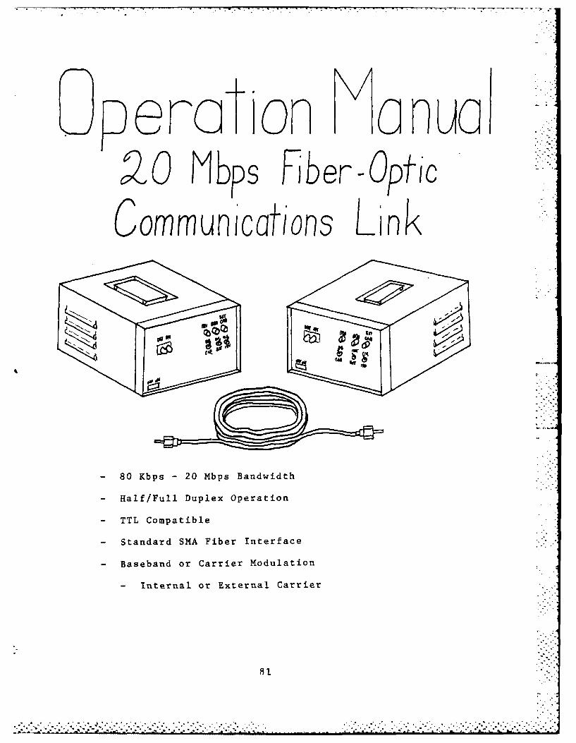
Oerac in H onaQO~~e >bsVeptic
Communications Link
- 80 Kbps -20 Mbps Bandwidth
- Half/Full Duplex Operation
- TTL Compatible
- Standard SMA Fiber Interface
- Baseband or Carrier Modulation
- Internal or External Carrier
This manual contains a technical description and oper-
ational information for this 20 Mbps Fiber-Optic Communications
Link. This manual is broken down into four parts. Section 1
is the technical description of the system. Section 2 covers
the theory of operation. Section 3 is the funtional des-
cription and directions for operation. And Section 4 contains
the schematics for all internal circuits except for the power
supplies, ECL Clock card, ECL/TTL Translator card and the
forced air cooling system.
Section 1.
This fiber optic data link is capable of transmitting
digital signals within the range of 80 Kbps to 20 Mbps. The
system has two basic modes of operation: simple baseband or
carrier modulation transmission. In the carrier modulation
mode either externally provided or internal carriers may be
used. Externally modulated signals can also be transmitted
by using the baseband mode of operation.
Electrical interface to the user's terminal equipment is
provided through standard BNd connectors on the front panel.
All inputs and outputs have TTL signalling levels. Transmission
mode selection is accomplished through the three switches
located directly below the BNC connectors on the front panel.
The optical interface is provided by a bulkhead mounted
Light Emitting Diode (LED) and Photodiode (PD). Both the
LED and PD have SMA styled receptors compatible with any
82

standard SMA styled fiber-optic connectors.
SPECIFICATIONS:
Power Requirements - 110 V ac., 60 Hz, 10.
Electrical Signallying Interface - Standard TTL,
through BNC connectors.
Optical Interface - Single strand optical fiber terminated
with SMA styled fiber optic Connectors.
OPTICAL CHARACTERISTICS:
LED Augat 698-013EG2
Edge Emitting LED
Specifications at 250 C., V c 5.OVcc
Min Reverse Breakdown Voltage 3.0 V
Foward Voltage, If = 100 mA 1.9 V
Wavelength 880 nm
FWHM 40 nm
Response Time 20 ns
LED Output Emisiion Radiation Pattern
- - '-IS '
Saur.,10- .-.- -
- -• - - - --+0" *FWHM = 6"
- -. 410"" -"
L, I I
dT -
83..........................................................
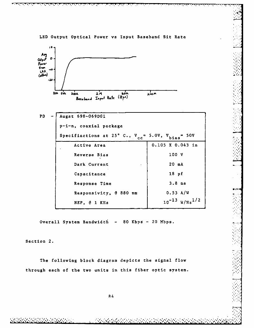
LED Output Optical Power vs Input Baseband Bit Rate
LED
PD -Augat 698-069DGI
p-i-n, coaxial package
Specifiactions at 250 C., V =5.0V, V50Vcc Vbis
Active Area 0.105 X 0.043 in
Reverse Bias 100OV
Dark Current .20 mA
Capacitance 18 pf
Response Time 3.8 ns
Responsivity, @880 nm 0.53 A/W
-13 1/2NE?, @1 KHz 10 W/Hz
Overall System Bandwidtfi -80 KbpA 20 Mbps.
Section 2.
The following block diagram depicts the signal flow
through each of the two units in this fiber optic system.
84
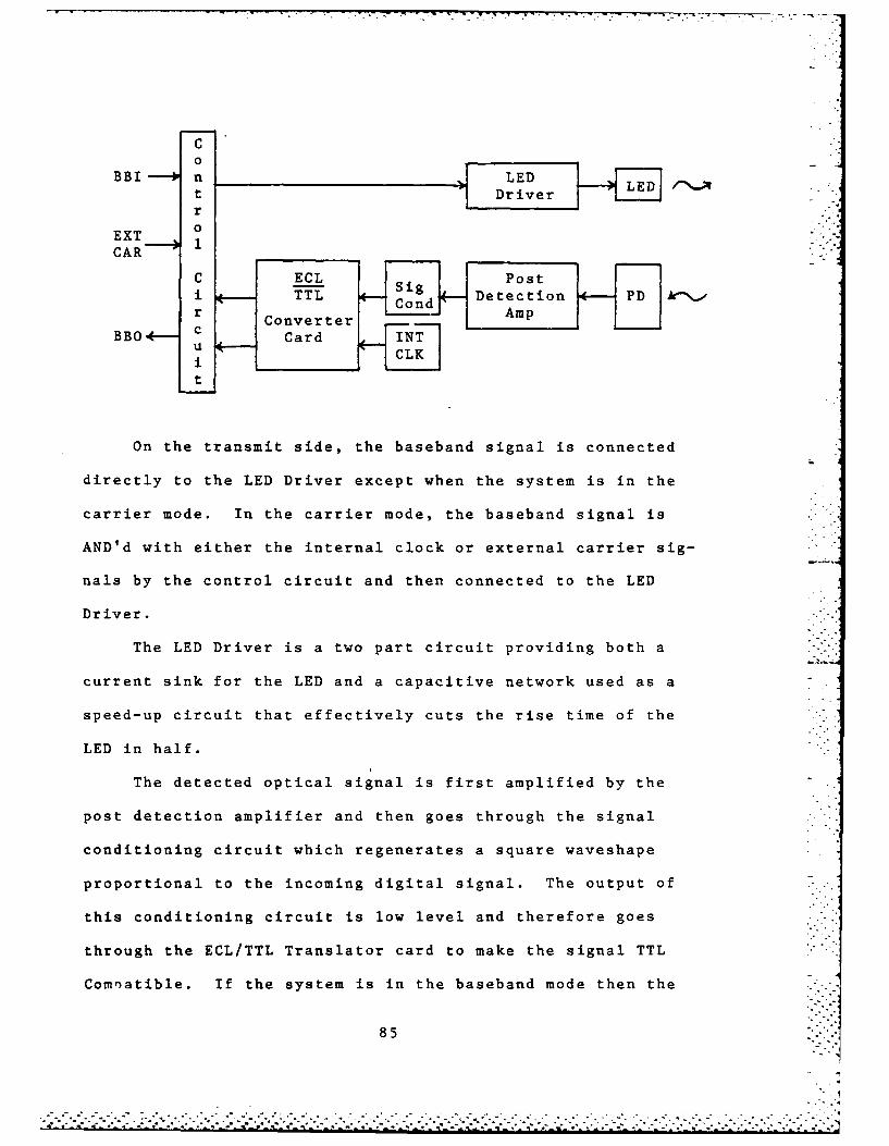
C0
BBI n _ LED 1-V-]t| Driver
r
EXTCAR 1C ECL Post
i TTL Sig Detection PD k%,
r Converter _______Amp
BBO4 c Card INT
i CLK
t
On the transmit side, the baseband signal is connected
directly to the LED Driver except when the system is in the
carrier mode. In the carrier mode, the baseband signal is -
AND'd with either the internal clock or external carrier sig-
nals by the control circuit and then connected to the LED
Driver.
The LED Driver is a two part circuit providing both a
current sink for the LED and a capacitive network used as a
speed-up circuit that effectively cuts the rise time of the
LED in half.
The detected optical signal is first amplified by the
post detection amplifier and then goes through the signal
conditioning circuit which regenerates a square waveshape
proportional to the incoming digital signal. The output of
this conditioning circuit is low level and therefore goes
through the ECL/TTL Translator card to make the signal TTL
Comnatible. If the system is in the baseband mode then the
85
- .- . - . . . . .. :. . . . . . . .- - - .. . ... . . .. . . . . . . -

received signal is connected directly to the output. If
the system is in the carrier mode, then the received signal
goes into a D-flip/flop that is triggered by either the
internal clock or external carrier, selected by the INT/EXT
selector switch. If the carrier signal is present then the
D-flip/flop eliminates the low half of the period by remaining
high for the entire carrier period. If the carrier is not
present, the output of the D-flip/flop remains low intil the
carrier returns. This circuit effectively demodulates the
carrier signal and then connects the signal to the output.
However, this demodulator circuit depends on very-accurate
local carrier frequencies.
Bandwidth limitations for this system stem from the
frequency response of both the LED Driver and the Post Detection
Amplifier and Circuit Conditioning circuits.
Section 3.
This fiber-optic system has three major useful config-
urations. First, a single unit can be looped back to itself
for local testing of a single fiber. Or the two units can be
connected with a single optical fiber to establish a simplex
mode of operation. Lastly, the two units can be connected with
two fibers to comprise a full duplex communications link, with
each side (transmit or receive) capable of sending up to 20
Mbps independently.
-2- - -7i
. ' .t , : t 2 - ,: '-: ." , . "/ . " - .- ' ' .''" -L -,-.''''. -, ''- . " "" -", .'" "". " - . . . " -' "","," - .""8 6. " . ".

Each of these three configurations can support both
modes of transmission; that is, direct baseband or carrier
modulation. To transmit either straight baseband or an exter-
nally modulated digital signals such as PDM, PPM or PCM
connect the input signal to the BBI BNC connector and put the
BB/CAR switch in the BB position. To transmit a carrier
modulated signal using the internal carrier connect the base-
band signal to the BBI BNC connector and put the BB/CAR switch
in the CAR position and the INT/EXT switch in the INT position.
To transmit a carrier modulated signal with an externally
provided carrier frequency again the baseband goes to the BBI
connector, the BB/CAR switch goes to the CAR position, but
the INT/EXT switch goes to the EXT position while the external
TTL carrier signal is connected to the EXT CAR ENC connector.
When the BB/CAR switch is in the BB position the other two
switches have no impact on the transmission regardless of their
positions. The CLK/INV switch is used as a simple receiver
synchronizer in either carrier modulation modes. If, because
of propagation delays, the demodulation circuit is sampling
the incoming signal in the low state of the carrier period
then the output of the system will always be low. Changing
the sense of the CLK/INV switch causes an effective 1800 phase
shift in the sampling signal and the carrier is then sampled
in the high part of its period and can then recreate the base-
band signal. Therefore if the system is in the carrier modula-
tion mode and the output remains low, changing the position of
87
---...-..........-... i-ii. .. ...-. ... . .... '-'-..-,- ,"-.l

k D-AiMl 794 WIDEBRND FIBER OPTIC COMMUNICATIONS LINK(U) AIR FORCE 2/2IINST OF TECH WRIGHT-PATTERSON AFB OH SCHOOL OFI ENGINEERING J R BRAY DEC 84 AFIT/GE/ENG/B4D-16
UNCLASSIFIED F/01712 NL
, m9 lm -11111
" UIIII
•0 1

p J°.
the CLK/INV switch should establish proper demodulation of the
signal.
This simple synchronization of carrier demodulation de-
pends on exact external carrier frequencies. The incoming
optical signal, after being detected, is sampled at the carrier
frequency selected by the INT/EXT switch. When the internal
carrier is used, the clock in the receiving unit is exact enough
to perform this operation. However, in the external carrier
mode there is no carrier tracking or synchronization circuits
and the signal is sampled at the rate provided by the external
carrier signal. Therefore in a laboratory environment the
same external carrier should be provided to each of the units
to avoid this shnchronization problem, and a long haul con-
figuration of these two units in the external carrier modulation
mode is not feasible.
Section 4.
This section contains schematics for the Control Circuit,
the LED Driver, the Post Detection Amplifier and the Circuit
Conditioning Cards. Schemattcs are not included for the two
remaining circuits because only the 20 MHz clock signal is used
from the bottom card and two ECL/TTL convertors are used from
the middle card. All logic gates on the Control Circuit are
standard TTL IC's, and on the other schematics all resistance
values are in ohms and all capacitance values are in microfarads.
88
" 88

Pin i
Pin 1'
S3
Contro/I Circuit
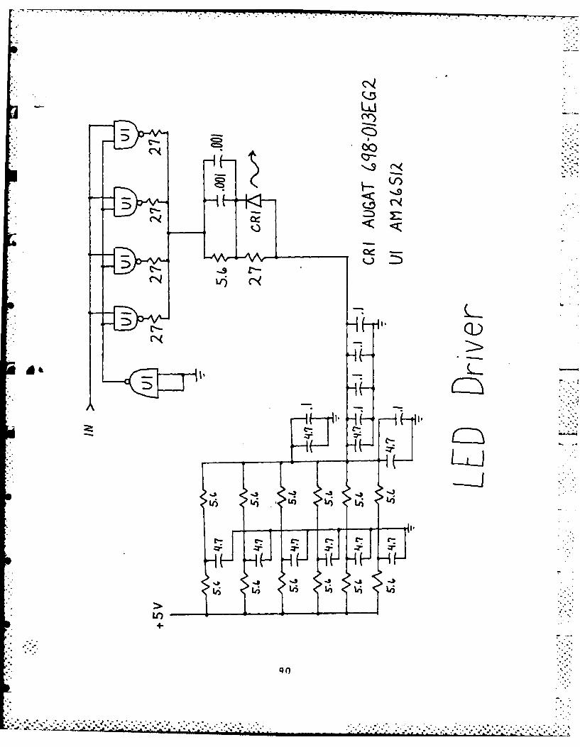
N-
(J-)J
q- .

390
.1 CR1I'iv
T o.OUT
-15 V
CRI I N52If ICRZ AL)GAT (698-O6qDGIUI RCA-CAjl2.7E
Pst Detecton Ampif ier
91
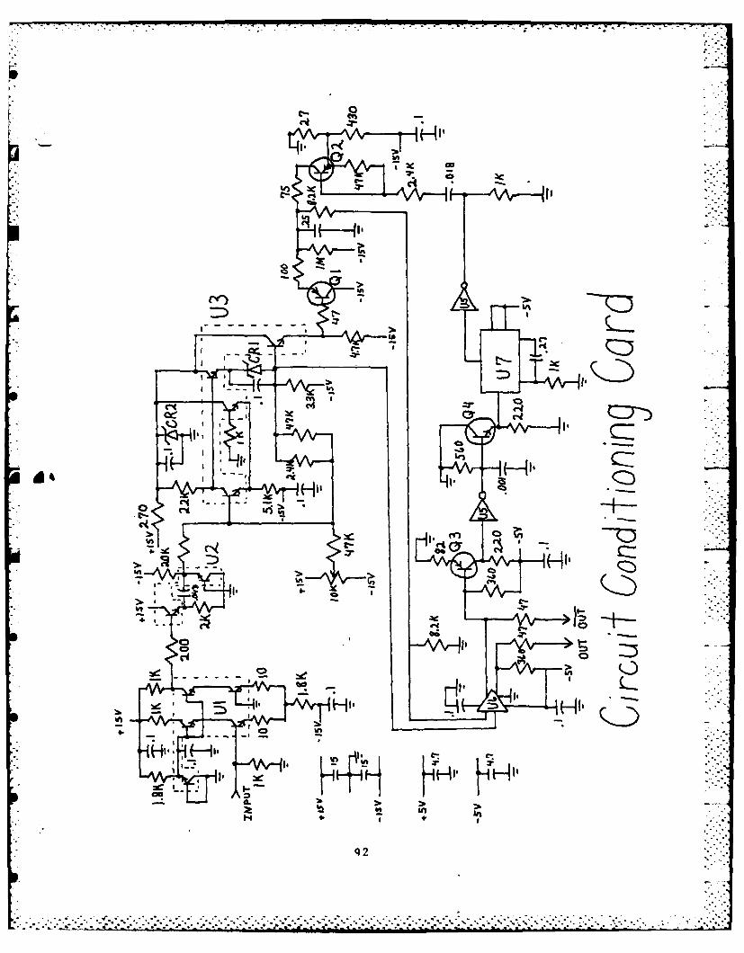
to- ess.
cli OHIOlot CC)
ci
kh>.
to
-a 21C
- -wt - - 7
C-4elf C-
Ln F-4 1IPA
C-4
Ileus
OA
Ott,
Alf
Ord
It His !H itL74
iIs Ile
4L
An
q2

CircuFt Condifl'on ins COrd
Q2.,Q3 2 N 301OQ~f 2.N3qo
CRI TRW' PD6 0205CR2 /A52/ii, U2,L}3 CA 3127E
UJ5 7906.
L}7 7N685DL
U73
- -. - . ---. - vI.. .. U -
Bibliography
1. Air Force Avionics Laboratory, Air Force Systems Command.EMI/EMP Resistant Data Bus. Report from Spectronics, Inc.,Richardson, Texas. AFAL-TR-76-99. Contract NumberF33615-74-C-1001, September, 1976.
2. Air Force Avionics Laboratory, Air Force Systems Command.Fiber Optic Link Improvement Program. Report fromSpectronics, Inc., Richardson, Texas. AFAL-TR-76-128.Contract Number F33615-77-C-1226, August, 1978.
3. Air Force Avionics Laboratory, Air Force Systems Command.Flight Operational Wideband Fiber Optic Data Links. Re-port from Spectronics, Inc., Richardson, Texas. AFAL-TR-77-54. Contract Number F33615-76-C-1047, November, 1977.
4. Air Force Avionics Laboratory, Air Force Systems Command.Wideband Fiber Optic Data Links. Report from Spectronics,Inc., Richardson, Texas. AFAL-TR-77-55. Contract NumberF33615-74-C-1160, October, 1977.
5. Doyle, Hank and Robert A. Wey. Augat Fiberoptics. Designand Operation of a Stable Attenuation Measurement System,May 1982. Augat Fiberoptics Components and Systems,Attleboro MA. 1982.
6. Duke, David A. and others. Optical Waveguide Performance/Cost Relationship: Special Report, undated. Telecommun-ications Products Dept., Corning Glass Works, Corning,New York.
7. F122-00077. Amphenol Fibre Optic Designer's Handbook.Product Catalog. Amphenol, Broadview IL, September 1982.
8. Fujii, Y. and others. "Precise Angular MisalignmentMeasurement in Optical Fiber Connector Plugs," ProgressIn Optical Communications, Vol I: 158-159 (1980).
9. Horiguchi, M. "Spectral Losses at Low-OH-Content OpticalFibers," Progress In Optical Communications, Vol I: 79-80(1980).
10. Keck, Donald B. "Single-mode Fibers Outperform MultimodeCables," IEEE Spectrum, Vol 20 30-37 (March 1983).
Q4
-. '.
:=. °o ' o o- °o . . .- o . .o . =o - . .= oO °- .* - o .. . . - . .. o- - - -3 . a n.. . . . . .' . -. . . . . .. ."-2 i

11. Keiser, Gerd. Optical Fiber Communications. New York:McGraw-Hill Book Company, 1983.
- 12. Kurokawa, T. and others. "Precisely Moulded PlasticSplices for Optical Fibers," Progress In Optical Commun-ications, Vol 11: 147-148 (1982).
13. LD-281BR. Light Emitting Diode. Product Description.Laser Diode Laboratories, New Brunswick NJ, undated.
14. LD-281CR. Laser Diode. Product Description. LaserDiode Laboratories, New Brunswick NJ, undated.
15. Noane, G. Le. "Low-Loss Optical-Fiber Sonnection Systems,"Progress In Optical Communications, Vol 1:114-115 (1980).
16. Osanai, H. and others. "Effects of Dopants on Trans-mission Loss of Low-OH-Content Optical Fibers," ProgressIn Optical Communications, Vol I: 80-81 (1980).
17. Rome Air Developement Center, Air Force Systems Command.Optical Cable Communications Study. Report from HarrisCorporation, Melbourne, Florida, RADC -TR-75-187. AirForce Contract Number F30602-74-C-0193, July, 1975.(AD-A 016846).
18. Satellite Branch, Communications Engineering Directorate,jt US Army Communications-Electronics Engineering Installation
Agency. Design Handbook for Optical Fiber Systems.Project Order Number CC-006-78. August, 1978. (ADA 061125).
19. Sudo, S. and others. "Low-OH-Content Optical FiberFabricated by Vapour-Phase Axial-Deposition," ProgressIn Optical Communications, Vol I: 103-104 (1980).
20. S104. Shortform Catalog. Product Catalog. Augat Inc.,Attleboro MA, August 1982.
21. Tsujimoto, Y. and others. "Fabrication of Low-Loss 3 dBCouplers With Multimode.'Optical Fibers," Progress InOptical Communications, Vol I: 157 (1980).
22. Wey, Robert A. General Manager, Augat Fiberoptics.Fiberoptic Communications: Technical Review, undated.Augat Fiberoptic Components and Systems, Attleboro Ma, 1982.
957

VITA
James Bray was born on 16 August 1950 in Louisville,
Kentucky. He graduated from Bishop David Memorial High
School in Louisville, Kentucky, in 1968, and enlisted in
the United States Air Force in November 1969. He attended
Texas Tech University under the Airman Education and
Commissioning Program, and he received the degree of Bachelor
of Science in Electrical Engineering. Upon graduation,
he attended Officer Training School and received a commission.
He was assigned as a test engineer in the Directorate of
Inertial Engineering, Aerospace Guidance and Metrology Center,
Newark APS, Ohio in May 1981. He then served as Chief, Mass
ja and Dimensional Standards Laboratory in the Directorate of
Metrology at Newark until entering the School of Engineering,
Air Force Institute of Technology, in June 1983.
Permanent Address: 10803 Torrington Rd.
Louisville, Kentucky 40272
96
• . . . .. . . . . . . . . . . . . . . . .. . . °

JNCLASSIFIED
ECURITY CLASSIFICATION OF THIS PAGE
REPORT DOCUMENTATION PAGEIa. REPORT SECURITY CLASSIFICATION lb. RESTRICTIVE MARKINGS
UNCLASSIFIEDSECURITY CLASSIFICATION AUTHORITY 3. DISTRIBUTION/AVAI LABILITY OF REPORT
Approved for public release;2b. DECLASSIFICATION/DOWNGRADING SCHEDULE distribution unlimited
4. PERFORMING ORGANIZATION REPORT NUMBER(S) 5. MONITORING ORGANIZATION REPORT NUMBER(S)
AFIT/GE/ENG/84D-16Ga. NAME OF PERFORMING ORGANIZATION rb. OFFICE SYMBOL 7a. NAME OF MONITORING ORGANIZATION
(If applicable)
School of Engineering AFIT/ENGGe. ADDRESS (City. State and ZIP Code) 7b ADDRESS (City, State and ZIP Code)
Air Force Institute of TechnologyWright-Patterson AFB, Ohio 45433
Be. NAME OF FUNDING/SPONSORING Ob. OFFICE SYMBOL 9. PROCUREMENT INSTRUMENT IDENTIFICATION NUMBERORGANIZATION (If applicable)
Sc. ADDRESS City. State and ZIP Code) 10. SOURCE OF FUNDING NOS.
PROGRAM PROJECT TASK WORK UNITELEMENT NO. NO. NO. NO.
11. TITLE (Include Security Claaification)
_Rpi- Bnx 1()
12. PERSONAL AUTHOR(S)
James R. Bray. B.S.. 1st Lt. USAF%'I& TYPE OF REPORT 13b. TIME COVERED 14. DATE OF REPORT 1Yr-. Mo.. Day) 15. PAGE COUNT
MS Thesis FROM _ TO 1984 December 10516. SUPPLEMENTARY NOTATION
17. COSATI CODES 18. SUBJECT TERMS (Continue on reuerse if necesary and identify by block number)
FIELD GROUP SUB. GR. Optical Communications17 8 Fiber Optics
Fiber Optics Transmission Lines19. ABSTRACT (Continue on reuerse if necesary and identify by block numbero
Title: WIDEBAND FIBER OPTIC COMMUNICATIONS LINK
Thesis Chairman: Vaqar Syed, PhD. -VH -, ,D.qa f,: ,'. P Dvelopmenf
Air force .. .. , A1C)
20. DISTRIBUTION/AVAILABILITY OF ABSTRACT 21. ABSTRACT SECURITY CLASSIFICATION
.NCLASSIFIEO/UNLIMITED X SAME AS RPT. C3 OTIC USERS C3 UNCLASSIFIF".
22& NAME OF RESPONSIBLE INDIVIDUAL 22b. TELEPHONE NUMBER 22c. OFFICE SYMBOL
Kenneth C. Castor, Major, USAF 51T- -515 AFITENG
DO FORM 1473, 83 APR EDITION OF 1 JAN 73 IS OBSOLETE. UNCLASSIFIEDSECURITY CLASSIFICATION OF THIS PAGE
" ........ "... .. .-...."'.,' .- . ,' - -." , " -. .,.-. i "" -- .- i "" ''. '' 'i,? ' . -,, -" - .-' -.L . ''-'
UNCLASSIFIED:URITY CLASSIFICATION OF THIS PAGE
A feasibility study was conducted on the possibility of .
upgrading a nine port fiber optic bundle telecommunicationssystem to a single strand fiber optic system. Usable piecesof equipment werc identified and new Light Emitting Diodes,Photodetectors and single strand SMA styled fiber optic con-nectors were ordered. Background research was conducted inthe area of fiber optic power launching, fiber losses, connec-tor losses and efficiences. A new modulation/demodulationcircuit was designed and constructed using parts from unusedequipment. A new front panel was constructed to house thecomponents, switches and connectors. A two meter piece ofoptical fiber was terminated with the new connectors and testedfor connector loss, numeric aperture and attenuation. Thenew Light Emitting Diode was characterized by its emissionradiation pattern and the entire system was tested for func-tional operation, frequency response and bandwidth of opera-tion. An Operations Manual was prepared to ensure proper usein the future. The result was a two piece, single strand, fi-ber optic communications system fully TTL compatible, capableof transmitting digital signals from 80 Kbit/sec to 20Mbit/sec. The system was tested in a half duplex mode usingboth baseband and carrier modulated signals. Utilizing bothpieces of the system full duplex operation was also demon-strated.
UNCLASSIFIEDSECURITY CLASSIFICATION OF THIS PAGE

FILMED
5-85
DTIC


![Threats to Fiber- Optic Infrastructures · lMCI targeting Verizon for brand damage [tap disclosures] ... Defending Fiber Optic InfrastructuresDefending Fiber Optic Infrastructures](https://cdn.vdocuments.us/doc/165x107/5acb82e77f8b9ab10a8b583f/threats-to-fiber-optic-targeting-verizon-for-brand-damage-tap-disclosures-.jpg)


