
Vivado Design Suite
Tutorial
Embedded Processor Hardware
Design
UG940 (v2018.1) April 04, 2018

Embedded Processor Hardware Design www.xilinx.com 2 UG940 (v2018.1) April 04, 2018
Revision History The following table shows the revision history for this document.
Section Revision Summary
04/04/2018 Version 2018.1
General updates Validated for 2018.1 release.
Send Feedback

Embedded Processor Hardware Design www.xilinx.com 3 UG940 (v2018.1) April 04, 2018
Table of Contents
Revision History .......................................................................................................................................................................... 2
Programming and Debugging Embedded Processors ..................................................................................................... 5
Introduction ................................................................................................................................................................................. 5
Hardware and Software Requirements .............................................................................................................................. 5
Tutorial Design Descriptions .................................................................................................................................................. 5
Locating Tutorial Design Files ............................................................................................................................................... 7
Lab 1: Building a Zynq-7000 AP SoC Processor Design ................................................................................................... 8
Introduction ................................................................................................................................................................................. 8
Step 1: Start the Vivado IDE and Create a Project ......................................................................................................... 8
Step 2: Create an IP Integrator Design ........................................................................................................................... 11
Step 3: Debugging the Block Design ............................................................................................................................... 17
Step 4: Generate HDL Design Files ................................................................................................................................... 20
Step 5: Implement Design and Generate Bitstream .................................................................................................. 22
Step 6: Export Hardware to SDK ........................................................................................................................................ 24
Step 7: Create a Software Application ............................................................................................................................ 25
Step 8: Run the Software Application ............................................................................................................................. 27
Step 9: Connect to the Vivado Logic Analyzer ............................................................................................................. 30
Conclusion ................................................................................................................................................................................. 35
Lab Files ...................................................................................................................................................................................... 35
Lab 2: Zynq-7000 AP SoC Cross-Trigger Design ............................................................................................................. 36
Introduction .............................................................................................................................................................................. 36
Step 1: Start the Vivado IDE and Create a Project ...................................................................................................... 36
Step 2: Create an IP Integrator Design ........................................................................................................................... 37
Step 3: Implement Design and Generate Bitstream .................................................................................................. 46
Step 4: Export Hardware to SDK ........................................................................................................................................ 47
Step 5: Build Application Code in SDK ............................................................................................................................ 48
Step 6: Connect to Vivado Logic Analyzer .................................................................................................................... 58
Send Feedback

Embedded Processor Hardware Design www.xilinx.com 4 UG940 (v2018.1) April 04, 2018
Step 7: Setting the Processor to Fabric Cross Trigger ............................................................................................... 60
Step 8: Setting the Fabric to Processor Cross-Trigger .............................................................................................. 63
Conclusion ................................................................................................................................................................................. 64
Lab Files ...................................................................................................................................................................................... 64
Lab 3: Using the Embedded MicroBlaze Processor ........................................................................................................ 65
Introduction .............................................................................................................................................................................. 65
Step 1: Invoke the Vivado IDE and Create a Project .................................................................................................. 66
Step 2: Create an IP Integrator Design ........................................................................................................................... 67
Step 3: Memory-Mapping the Peripherals in IP Integrator .................................................................................... 80
Step 4: Validate Block Design ............................................................................................................................................. 82
Step 5: Generate Output Products ................................................................................................................................... 82
Step 6: Create a Top-Level Verilog Wrapper ................................................................................................................ 84
Step 7: Take the Design through Implementation ..................................................................................................... 84
Step 8: Exporting the Design to SDK ............................................................................................................................... 85
Step 9: Create a “Peripheral Test” Application ............................................................................................................. 86
Step 10: Executing the Software Application on a KC705 Board .......................................................................... 92
Step 11: Connect to Vivado Logic Analyzer .................................................................................................................. 97
Step 12: Setting the MicroBlaze to Logic Cross Trigger ........................................................................................... 99
Step 13: Setting the Logic to Processor Cross-Trigger ........................................................................................... 102
Conclusion ............................................................................................................................................................................... 103
Lab Files .................................................................................................................................................................................... 103
Legal Notices ............................................................................................................................................................................... 104
Please Read: Important Legal Notices .......................................................................................................................... 104
Send Feedback
Embedded Processor Hardware Design www.xilinx.com 5 UG940 (v2018.1) April 04, 2018
Programming and Debugging Embedded Processors
Introduction This tutorial shows how to build a basic Zynq®-7000 All Programmable (AP) SoC processor and a
MicroBlaze™ processor design using the Vivado® Integrated Development Environment (IDE).
In this tutorial, you use the Vivado IP integrator tool to build a processor design, and then debug the
design with the Xilinx® Software Development Kit (SDK) and the Vivado Integrated Logic Analyzer.
IMPORTANT: The Vivado IP integrator is the replacement for Xilinx Platform Studio (XPS) for embedded
processor designs, including designs targeting Zynq-7000 AP SoC devices and MicroBlaze™ processors.
XPS only supports designs targeting MicroBlaze processors, not Zynq-7000 AP SoC devices.
Hardware and Software Requirements This tutorial requires that Vivado Design Suite software (System Edition) release is installed. See the
Vivado Design Suite User Guide: Release Notes, Installation, and Licensing (UG973) for a complete list
and description of the system and software requirements.
The following Platform boards and cables are also needed:
Xilinx Zynq-7000 AP SoC ZC702 board for Lab 1, and Lab 2
Xilinx Kintex – 7 KC705 board for Lab 3
One USB (Type A to Type B)
JTAG platform USB Cable or Digilent Cable
Power cable to the board
Tutorial Design Descriptions No design files are required for these labs, if step-by-step instructions are followed as outlined;
however, for subsequent iterations of the design or to build the design quickly, Tcl command files for
these labs are provided. For cross-probing hardware and software, manual interaction with Vivado and
Platform boards is necessary. No Tcl files are provided for that purpose.
Send Feedback

Programming and Debugging Embedded Processors
Embedded Processor Hardware Design www.xilinx.com 6 UG940 (v2018.1) April 04, 2018
Lab 1: Building a Zynq-7000 AP SoC Processor
Lab 1: Building a Zynq-7000 AP SoC Processor Design uses the Zynq-7000 AP SoC Processing Subsystem
(PS) IP, and two peripherals that are instantiated in the Programmable Logic (PL) and connected using
the AXI Interconnect. The Lab uses the following IP in the PL:
A General Purpose IO (GPIO)
A Block Memory
An AXI BRAM Controller
Lab 1 shows how to graphically build a design in the Vivado IP integrator and use the Designer
Assistance feature to connect the IP to the Zynq-7000 AP SoC PS.
After you construct the design, you mark nets for debugging the logic. Then you generate the
Hardware Design Language (HDL) for the design as well as for the IP. Finally, you implement the design
and generate a bitstream, then export the hardware description of the design to the Software
Development Kit (SDK). You will use the SDK software to build and debug the design software, and
learn how to connect to the hardware server (hw_server) application that SDK uses to communicate
with the Zynq-7000 AP SoC processors. Then you perform logic analysis on the design with a connected
board.
Design Files
The following design files are included in the zip file for this guide:
lab1.tcl
See Locating Tutorial Design Files.
Lab 2: Zynq-7000 AP SoC Cross Trigger Design
Lab 2: Zynq-7000 AP SoC Cross-Trigger Design requires that you have the Software Development Kit
(SDK) software installed on your machine.
In Lab 2, you use the SDK software to build and debug the design software, and learn how to connect
to the hardware server (hw_server) application that SDK uses to communicate with the Zynq-7000 AP
SoC processors. Then, use the cross-trigger feature of the Zynq-7000 AP SoC processor to perform logic
analysis on the design on the target hardware.
Design Files
The following design files are included in the zip file for this guide:
lab2.tcl
See Locating Tutorial Design Files.
Send Feedback
Programming and Debugging Embedded Processors
Embedded Processor Hardware Design www.xilinx.com 7 UG940 (v2018.1) April 04, 2018
Lab 3: Programming a MicroBlaze Processor
Lab 3: Using the Embedded MicroBlaze Processor uses the Xilinx MicroBlaze processor in the Vivado IP
integrator to create a design and perform the same export to SDK, software design, and logic analysis.
Design Files
The following design files are included in the zip file for this guide:
lab3.tcl
See Locating Tutorial Design Files.
Locating Tutorial Design Files Design data is in the associated Reference Design File.
This document refers to the design data as <Design_Files>.
Send Feedback

Embedded Processor Hardware Design www.xilinx.com 8 UG940 (v2018.1) April 04, 2018
Lab 1: Building a Zynq-7000 AP SoC Processor Design
Introduction In this lab you create a Zynq®-7000 AP SoC processor based design and instantiate IP in the processing
logic fabric (PL) to complete your design. Then you mark signals to debug in the Vivado® Logic
Analyzer. Finally, you take the design through implementation, generate a bitstream, and export the
hardware to SDK. In SDK you create a Software Application that can be run on the target hardware.
Breakpoints are added to the code to cross-probe between hardware and software.
If you are not familiar with the Vivado Integrated Development Environment Vivado (IDE), see the
Vivado Design Suite User Guide: Using the Vivado IDE (UG893).
Step 1: Start the Vivado IDE and Create a Project 1. Start the Vivado IDE by clicking the Vivado desktop icon or by typing vivado at a terminal
command line.
2. From the Quick Start section, click Create Project, as shown in the the following figure:
Figure 1: Vivado Quick Start Page
Send Feedback

Lab 1: Building a Zynq-7000 AP SoC Processor Design
Embedded Processor Hardware Design www.xilinx.com 9 UG940 (v2018.1) April 04, 2018
The New Project wizard opens.
Figure 2: Create New Project Wizard
3. Click Next.
The Project Name dialog box opens.
4. In the Project Name dialog box, type a project name and select a location for the project files.
Ensure that the Create project subdirectory check box is checked, and then click Next.
5. In the Project Type dialog box, select RTL Project, and then click Next.
6. In the Add Sources dialog box, set the Target language to your desired language, Simulator
language to Mixed and then click Next.
7. In the Add Constraints dialog box, click Next.
8. In the Default Part dialog box:
a. Select Boards.
b. From the Board Rev drop-down list, select All to view all versions of the supported boards.
c. Choose the version of the ZYNQ-7 ZC702 Evaluation Board that you are using.
d. Click Next.
Send Feedback

Lab 1: Building a Zynq-7000 AP SoC Processor Design
Embedded Processor Hardware Design www.xilinx.com 10 UG940 (v2018.1) April 04, 2018
Figure 3: New Project:Default Part Dialog Box
CAUTION! Multiple versions of boards are supported in Vivado. Ensure that you are
targeting the design to the right hardware.
9. Review the project summary in the New Project Summary dialog box, and then click Finish to
create the project.
Send Feedback

Lab 1: Building a Zynq-7000 AP SoC Processor Design
Embedded Processor Hardware Design www.xilinx.com 11 UG940 (v2018.1) April 04, 2018
Step 2: Create an IP Integrator Design 1. In the Flow Navigator > IP Integrator, select Create Block Design.
2. In the Create Block Design dialog box, specify a name for your IP subsystem design such as
zynq_design_1. Leave the Directory field set to the default value of <Local to Project>, and
leave the Specify source set field to its default value of Design Sources.
Figure 4: Create Block Design Dialog Box
3. Click OK.
4. In the block design canvas right-click, and select Add IP.
Alternatively, you can click the Add IP button in the IP integrator canvas.
Figure 5: Add IP Link in IP Integrator Canvas
The IP catalog opens.
5. In the search field, type to find the ZYNQ7 Processing System IP.
6. In the IP catalog, select the ZYNQ7 Processing System, and press Enter on the keyboard to add it
to your design.
In the Tcl Console, you see the following message:
create_bd_cell -type ip -vlnv xilinx.com:ip:processing_system7:5.5
processing_system7_0
There is a corresponding Tcl command for most actions performed in the IP integrator block design.
Those commands are not shown in this document; instead, the tutorial provides Tcl scripts to run
each lab.
Send Feedback

Lab 1: Building a Zynq-7000 AP SoC Processor Design
Embedded Processor Hardware Design www.xilinx.com 12 UG940 (v2018.1) April 04, 2018
Note: Tcl commands are documented in the Vivado Design Suite Tcl Command Reference Guide
(UG835).
7. In the IP Integrator window, click the Run Block Automation link.
Figure 6: Run Block Automation link
The Run Block Automation dialog box opens, stating that the FIXED_IO, and DDR interfaces will be
created for the Zynq-7000 AP SoC IP core. Also, note that the Apply Board Preset check box is
checked. This is because the selected target board is ZC702.
8. Ensure that both Cross Trigger In and Cross Trigger Out are disabled.
Figure 7: Zynq-7 Run Block Automation Dailog Box
9. Click OK.
Send Feedback

Lab 1: Building a Zynq-7000 AP SoC Processor Design
Embedded Processor Hardware Design www.xilinx.com 13 UG940 (v2018.1) April 04, 2018
After running block automation on the Zynq-7000 AP SoC processor, the IP integrator diagram looks
as follows:
Figure 8: Zynq-7000 AP SoC Processing System after Running Block Automation
Now you can add peripherals to the processing logic (PL).
10. Right-click in the IP integrator diagram, and select Add IP.
11. In the search field, type gpi to find the AXI GPIO, and then press Enter to add it to the design.
12. Similarly, add the AXI BRAM Controller.
Your Block Design window will look like the following figure. The relative positions of the IP might
vary.
TIP: You can zoom in and out in the Diagram Panel using the Zoom In ( or Ctrl+=) and
Zoom Out ( or Ctrl+-) tools.
Figure 9: Block Design after Instantiating IP
Send Feedback
Lab 1: Building a Zynq-7000 AP SoC Processor Design
Embedded Processor Hardware Design www.xilinx.com 14 UG940 (v2018.1) April 04, 2018
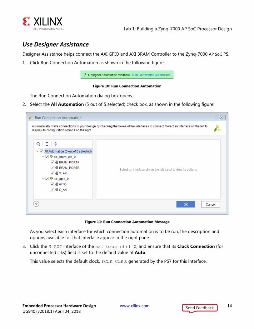
Use Designer Assistance
Designer Assistance helps connect the AXI GPIO and AXI BRAM Controller to the Zynq-7000 AP SoC PS.
1. Click Run Connection Automation as shown in the following figure:
Figure 10: Run Connection Automation
The Run Connection Automation dialog box opens.
2. Select the All Automation (5 out of 5 selected) check box, as shown in the following figure:
Figure 11: Run Connection Automation Message
As you select each interface for which connection automation is to be run, the description and
options available for that interface appear in the right pane.
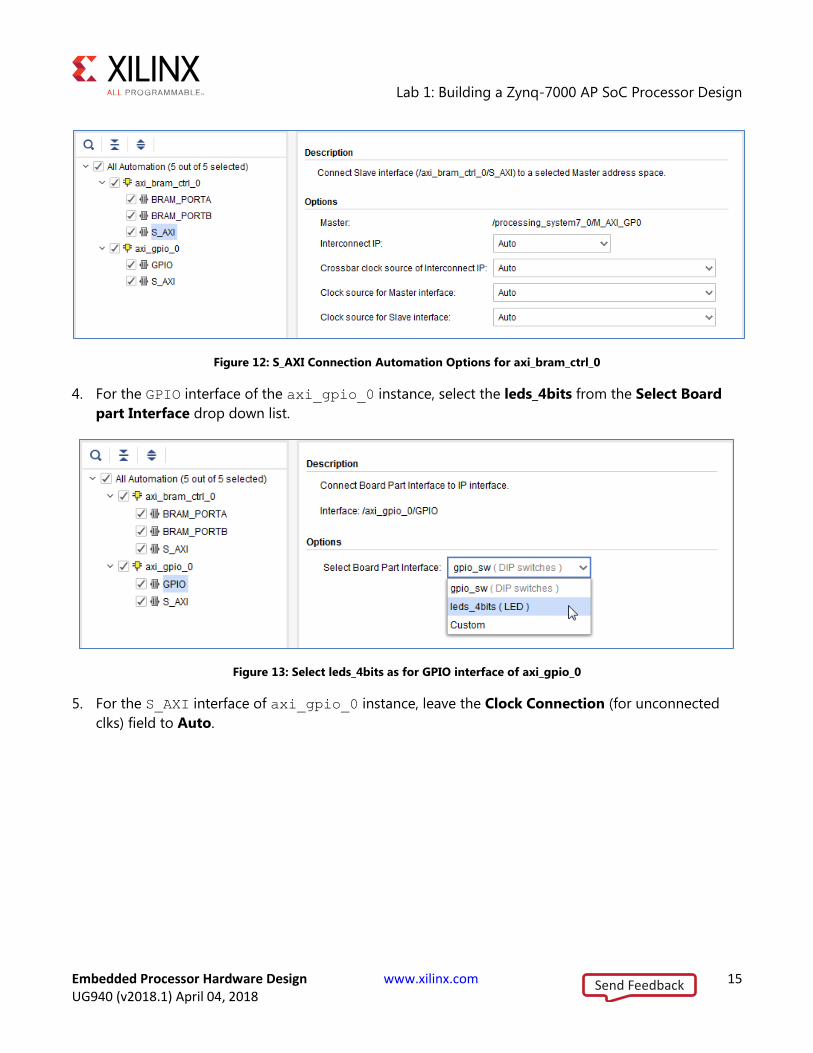
3. Click the S_AXI interface of the axi_bram_ctrl_0, and ensure that its Clock Connection (for
unconnected clks) field is set to the default value of Auto.
This value selects the default clock, FCLK_CLK0, generated by the PS7 for this interface.
Send Feedback
Lab 1: Building a Zynq-7000 AP SoC Processor Design
Embedded Processor Hardware Design www.xilinx.com 15 UG940 (v2018.1) April 04, 2018
Figure 12: S_AXI Connection Automation Options for axi_bram_ctrl_0
4. For the GPIO interface of the axi_gpio_0 instance, select the leds_4bits from the Select Board
part Interface drop down list.
Figure 13: Select leds_4bits as for GPIO interface of axi_gpio_0
5. For the S_AXI interface of axi_gpio_0 instance, leave the Clock Connection (for unconnected
clks) field to Auto.
Send Feedback

Lab 1: Building a Zynq-7000 AP SoC Processor Design
Embedded Processor Hardware Design www.xilinx.com 16 UG940 (v2018.1) April 04, 2018
Figure 14: Run Connection Automation Dialog Box for GPIO Interface of axi_gpio_0
6. Click OK.
The IP integrator subsystem looks like the following figure. The relative positions of the IP might
differ slightly.
Figure 15: Zynq-7000 AP SoC Processor System and Peripherals
7. Click the Address Editor tab and expand the processing_system7_0 hierarchy to show the
memory-map of the IP in the design.
In this case, there are two IP: the AXI GPIO and the AXI BRAM Controller. The IP integrator assigns
the memory maps for these IP automatically. You can change them if necessary.
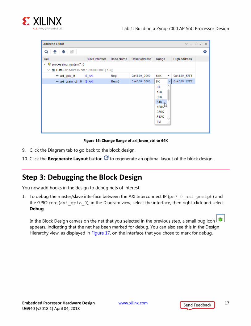
8. Change the range of the AXI BRAM Controller to 64K, as shown in Figure 16.
Send Feedback
Lab 1: Building a Zynq-7000 AP SoC Processor Design
Embedded Processor Hardware Design www.xilinx.com 17 UG940 (v2018.1) April 04, 2018
Figure 16: Change Range of axi_bram_ctrl to 64K
9. Click the Diagram tab to go back to the block design.
10. Click the Regenerate Layout button to regenerate an optimal layout of the block design.
Step 3: Debugging the Block Design You now add hooks in the design to debug nets of interest.
1. To debug the master/slave interface between the AXI Interconnect IP (ps7_0_axi_periph) and
the GPIO core (axi_gpio_0), in the Diagram view, select the interface, then right-click and select
Debug.
In the Block Design canvas on the net that you selected in the previous step, a small bug icon
appears, indicating that the net has been marked for debug. You can also see this in the Design
Hierarchy view, as displayed in Figure 17, on the interface that you chose to mark for debug.
Send Feedback

Lab 1: Building a Zynq-7000 AP SoC Processor Design
Embedded Processor Hardware Design www.xilinx.com 18 UG940 (v2018.1) April 04, 2018
Figure 17: Design Hierarchy: Bug Icon on Nets being Debugged
When a net is marked for debug, the Designer Assistance link in the banner of the block design
canvas becomes active.
2. Click Run Connection Automation.
The All Automation is selected by default with the various options for AXI Read/Write signals set, as
shown in the following figure:
Figure 18: Run Connection Automation Dialog box for inserting a System ILA IP
3. Click OK.
Send Feedback

Lab 1: Building a Zynq-7000 AP SoC Processor Design
Embedded Processor Hardware Design www.xilinx.com 19 UG940 (v2018.1) April 04, 2018
A System ILA IP is instantiated on the block design which is appropriately configured to debug the
AXI Interface marked for debug. The net marked for debug is connected to this System ILA IP and
an appropriate clock source is connected to the clk pin of the System ILA IP. The clock source is
the same clock domain to which the interface signal belongs
Figure 19: System ILA IP Connected to the Interface Net Being Debugged
4. From the toolbar, run Design-Rules-Check (DRC) by clicking the Validate Design button .
Alternatively, you can do the same from the menu by:
o Selecting Tools > Validate Design from the menu.
o Right-clicking in the Diagram window and selecting Validate Design.
The Validate Design dialog box opens to notify you that there are no errors or critical warnings in
the design.
The Tcl Console shows the following warning.
WARNING: [BD 41-1781] Updates have been made to one or more nets/interface
connections marked for debug.
Debug nets, which are already connected to System ILA IP core in the block-
design, will be automatically available for debug in Hardware Manager.
For unconnected Debug nets, please open synthesized design and use 'Set Up
Debug' wizard to insert, modify or delete Debug Cores. Failure to do so could
result in critical warnings and errors in the implementation flow.
Send Feedback
Lab 1: Building a Zynq-7000 AP SoC Processor Design
Embedded Processor Hardware Design www.xilinx.com 20 UG940 (v2018.1) April 04, 2018
Block designs can use the instantiation flow, where a System ILA or ILA IP is instantiated in the block
design, or they can use the netlist insertion flow, where nets are only marked for debug but the
debug core is inserted post-synthesis. This warning message can be ignored if the instantiation flow
is being used (as in this lab).
5. Click OK.
6. From the Vivado menu, save the block design by selecting File > Save Block Design.
Alternatively, you can press Ctrl + S to save your block design or click the Save button in the
Vivado toolbar.
Step 4: Generate HDL Design Files You now generate the HDL files for the design.
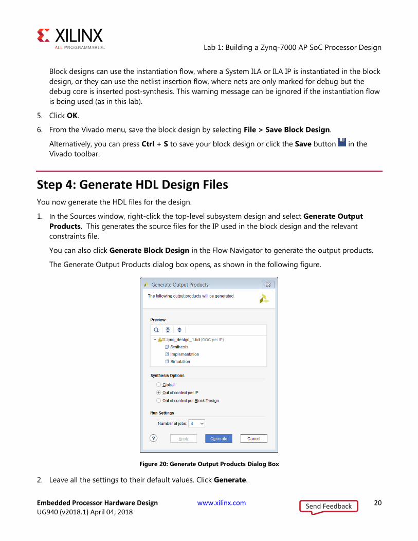
1. In the Sources window, right-click the top-level subsystem design and select Generate Output
Products. This generates the source files for the IP used in the block design and the relevant
constraints file.
You can also click Generate Block Design in the Flow Navigator to generate the output products.
The Generate Output Products dialog box opens, as shown in the following figure.
Figure 20: Generate Output Products Dialog Box
2. Leave all the settings to their default values. Click Generate.
Send Feedback
Lab 1: Building a Zynq-7000 AP SoC Processor Design
Embedded Processor Hardware Design www.xilinx.com 21 UG940 (v2018.1) April 04, 2018
3. The Generate Output Products dialog box opens informing that Out-of-context runs were launched.
4. Click OK.
5. Out-of-context runs can take a few minutes to finish. You can see the status of the runs by clicking
on the Design Runs tab at the bottom of the Vivado IDE.
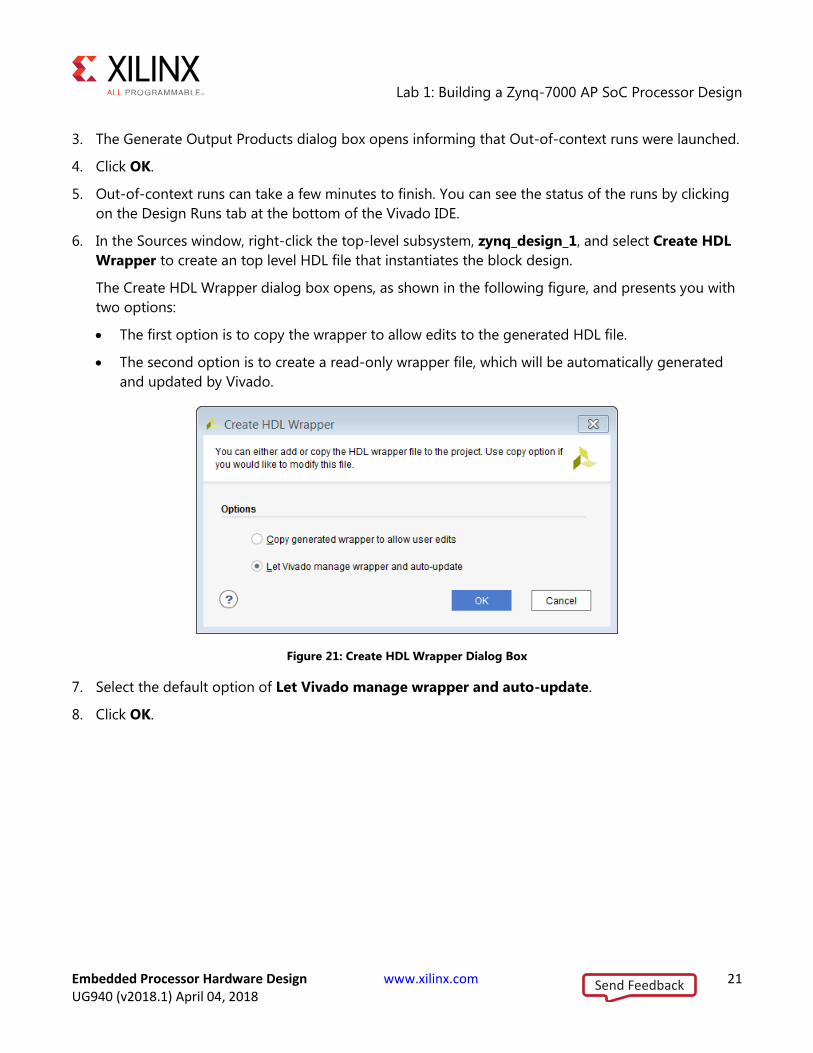
6. In the Sources window, right-click the top-level subsystem, zynq_design_1, and select Create HDL
Wrapper to create an top level HDL file that instantiates the block design.
The Create HDL Wrapper dialog box opens, as shown in the following figure, and presents you with
two options:
The first option is to copy the wrapper to allow edits to the generated HDL file.
The second option is to create a read-only wrapper file, which will be automatically generated
and updated by Vivado.
Figure 21: Create HDL Wrapper Dialog Box
7. Select the default option of Let Vivado manage wrapper and auto-update.
8. Click OK.
Send Feedback

Lab 1: Building a Zynq-7000 AP SoC Processor Design
Embedded Processor Hardware Design www.xilinx.com 22 UG940 (v2018.1) April 04, 2018
After the wrapper has been created, the Sources window looks as follows.
Figure 22: Source Window After Creating the Wrapper
Step 5: Implement Design and Generate Bitstream 1. In Flow Navigator > Program and Debug, click Generate Bitstream to implement the design and
generate a BIT file.
The No Implementation Results Available dialog box opens.
2. Click Yes.
3. The Launch Runs dialog box opens. Here you can select various options such as the Number of
Jobs, the host where the Runs are launched etc.
4. Click OK.
This will launch synthesis, implementation and generate the bitstream which could take a few
minutes.
Send Feedback
Lab 1: Building a Zynq-7000 AP SoC Processor Design
Embedded Processor Hardware Design www.xilinx.com 23 UG940 (v2018.1) April 04, 2018
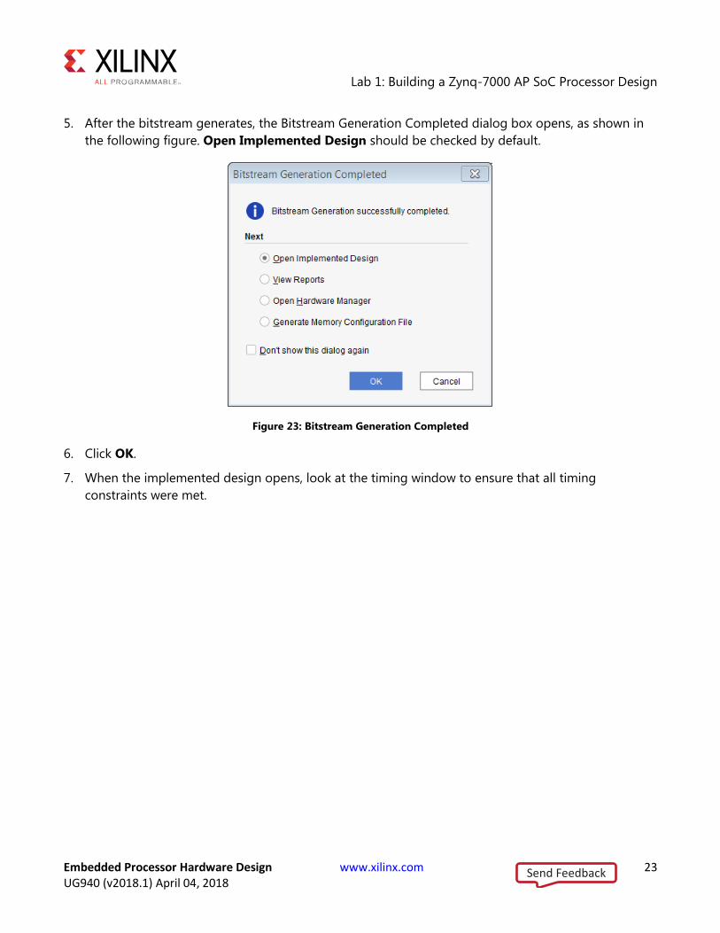
5. After the bitstream generates, the Bitstream Generation Completed dialog box opens, as shown in
the following figure. Open Implemented Design should be checked by default.
Figure 23: Bitstream Generation Completed
6. Click OK.
7. When the implemented design opens, look at the timing window to ensure that all timing
constraints were met.
Send Feedback

Lab 1: Building a Zynq-7000 AP SoC Processor Design
Embedded Processor Hardware Design www.xilinx.com 24 UG940 (v2018.1) April 04, 2018
Step 6: Export Hardware to SDK In this step, you export the hardware description to SDK.
IMPORTANT: For the Digilent driver to install, you must power on and connect the board to the host PC before
launching SDK.
1. From the main Vivado File menu, select File > Export > Export Hardware.
The Export Hardware dialog box opens.
2. Ensure that the Include Bitstream check box is checked and that the Export to field is set to the
default option of <Local to Project> as shown in the following figure:
Figure 24: Export Hardware for SDK
3. Click OK.
4. To launch SDK, select File > Launch SDK.
The Launch SDK dialog box opens.
5. Accept the default selections for Exported location and Workspace and click OK.
Figure 25: Launch SDK Dialog Box
Send Feedback

Lab 1: Building a Zynq-7000 AP SoC Processor Design
Embedded Processor Hardware Design www.xilinx.com 25 UG940 (v2018.1) April 04, 2018
Step 7: Create a Software Application SDK launches in a separate window.
1. Select File > New > Application Project.
The New Project dialog box opens.
2. In the Project Name field, type the name desired, such as Zynq_Design.
Figure 26: SDK Application Project
3. Click Next.
Send Feedback

Lab 1: Building a Zynq-7000 AP SoC Processor Design
Embedded Processor Hardware Design www.xilinx.com 26 UG940 (v2018.1) April 04, 2018
4. From the Available Templates, select Peripheral Tests as shown in the following figure:
Figure 27: SDK New Project Template
5. Click Finish.
When the program finishes compiling, you see the following in the Console window.
Figure 28: SDK Message
Send Feedback

Lab 1: Building a Zynq-7000 AP SoC Processor Design
Embedded Processor Hardware Design www.xilinx.com 27 UG940 (v2018.1) April 04, 2018
Step 8: Run the Software Application Now, run the peripheral test application on the ZC702 board. To do so, you need to configure the JTAG
port.
1. Ensure that your hardware is powered on and a Digilent Cable or the USB Platform Cable is
connected to the host PC. Also, ensure that you have a USB cable connected to the UART port of
the ZC702 board.
2. Download the bitstream into the FPGA by selecting Xilinx > Program FPGA.
The Program FPGA dialog box opens.
3. Ensure that the Bitstream field shows the bitstream file that you created in Step 5, and then click
Program.
Note: The DONE LED on the board turns green if the programming is successful. You should also see
an INFO message suggesting that the FPGA was configured successfully in the SDK Log window.
4. In the Project Explorer, select and right-click the Zynq_Design application.
5. Select Debug As > Debug Configurations.
6. In the Debug Configurations dialog box, right-click Xilinx C/C++ application (System Debugger)
and select New.
7. In the Debug Configurations dialog box, click Debug, as shown in the following figure:
Figure 29: Run Debug Configurations
The Confirm Perspective Switch dialog box opens.
Send Feedback
Lab 1: Building a Zynq-7000 AP SoC Processor Design
Embedded Processor Hardware Design www.xilinx.com 28 UG940 (v2018.1) April 04, 2018
8. Click Yes.
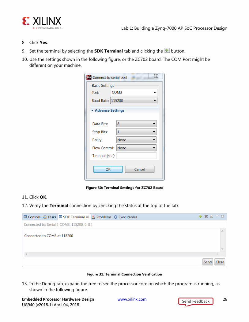
9. Set the terminal by selecting the SDK Terminal tab and clicking the button.
10. Use the settings shown in the following figure, or the ZC702 board. The COM Port might be
different on your machine.
Figure 30: Terminal Settings for ZC702 Board
11. Click OK.
12. Verify the Terminal connection by checking the status at the top of the tab.
Figure 31: Terminal Connection Verification
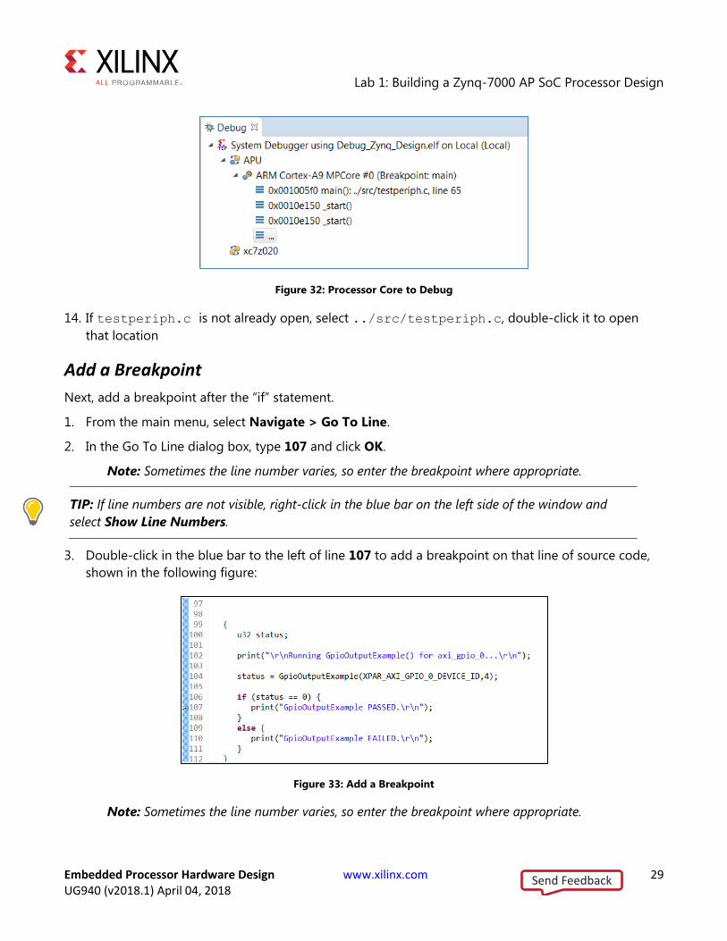
13. In the Debug tab, expand the tree to see the processor core on which the program is running, as
shown in the following figure:
Send Feedback
Lab 1: Building a Zynq-7000 AP SoC Processor Design
Embedded Processor Hardware Design www.xilinx.com 29 UG940 (v2018.1) April 04, 2018
Figure 32: Processor Core to Debug
14. If testperiph.c is not already open, select ../src/testperiph.c, double-click it to open
that location
Add a Breakpoint
Next, add a breakpoint after the “if” statement.
1. From the main menu, select Navigate > Go To Line.
2. In the Go To Line dialog box, type 107 and click OK.
Note: Sometimes the line number varies, so enter the breakpoint where appropriate.
TIP: If line numbers are not visible, right-click in the blue bar on the left side of the window and
select Show Line Numbers.
3. Double-click in the blue bar to the left of line 107 to add a breakpoint on that line of source code,
shown in the following figure:
Figure 33: Add a Breakpoint
Note: Sometimes the line number varies, so enter the breakpoint where appropriate.
Send Feedback

Lab 1: Building a Zynq-7000 AP SoC Processor Design
Embedded Processor Hardware Design www.xilinx.com 30 UG940 (v2018.1) April 04, 2018
Step 9: Connect to the Vivado Logic Analyzer 1. Connect to the ZC702 board using the Vivado® logic analyzer.
2. Go back to the Vivado session and from the Program and Debug drop-down list in the Flow
Navigator > Program and Debug, click Open Hardware Manager.
3. In the Hardware Manager window, click Open target and select Open New Target to open a
connection to the Digilent JTAG cable for ZC702, as shown below.
Figure 34: Launch Open New Hardware Target Wizard
The Open New Hardware Target dialog box opens.
4. Click Next.
5. Select the appropriate options from the drop down menu for Connect to option. Click Next on the
Hardware Server Settings page.
6. The hardware server should be able to identify the hardware target. Click Next on the Select
Hardware Target page.
7. Click Finish in the Open Hardware Target Summary page.
Send Feedback

Lab 1: Building a Zynq-7000 AP SoC Processor Design
Embedded Processor Hardware Design www.xilinx.com 31 UG940 (v2018.1) April 04, 2018
When the Vivado hardware session successfully connects to the ZC702 board, the Hardware window
shows the following information:
Figure 35: Successfully Programmed Hardware Session
8. First, ensure that the ILA core is active and capturing data. To do this, select the Status tab of the
hw_ila_1 in the Hardware Manager.
9. Click the Run Trigger Immediate button on the hw_ila_1 window.
Figure 36: Run Trigger Immediate to capture static data
Send Feedback
Lab 1: Building a Zynq-7000 AP SoC Processor Design
Embedded Processor Hardware Design www.xilinx.com 32 UG940 (v2018.1) April 04, 2018
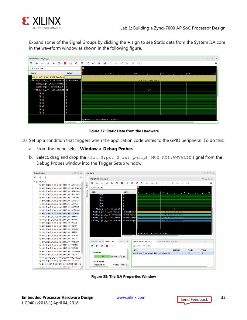
Expand some of the Signal Groups by clicking the + sign to see Static data from the System ILA core
in the waveform window as shown in the following figure.
Figure 37: Static Data from the Hardware
10. Set up a condition that triggers when the application code writes to the GPIO peripheral. To do this:
a. From the menu select Window > Debug Probes.
b. Select, drag and drop the slot_0:ps7_0_axi_periph_M00_AXI:AWVALID signal from the
Debug Probes window into the Trigger Setup window.
Figure 38: The ILA Properties Window
Send Feedback
Lab 1: Building a Zynq-7000 AP SoC Processor Design
Embedded Processor Hardware Design www.xilinx.com 33 UG940 (v2018.1) April 04, 2018
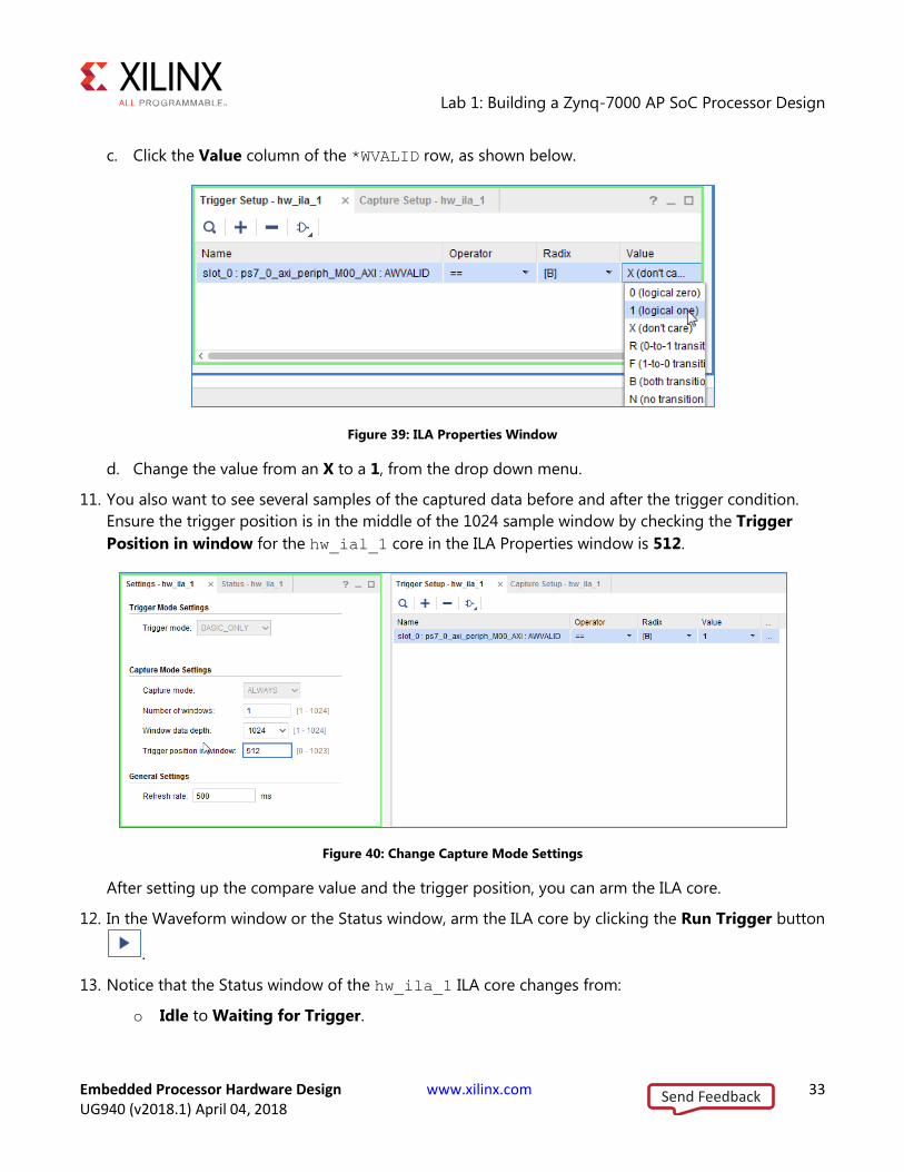
c. Click the Value column of the *WVALID row, as shown below.
Figure 39: ILA Properties Window
d. Change the value from an X to a 1, from the drop down menu.
11. You also want to see several samples of the captured data before and after the trigger condition.
Ensure the trigger position is in the middle of the 1024 sample window by checking the Trigger
Position in window for the hw_ial_1 core in the ILA Properties window is 512.
Figure 40: Change Capture Mode Settings
After setting up the compare value and the trigger position, you can arm the ILA core.
12. In the Waveform window or the Status window, arm the ILA core by clicking the Run Trigger button
.
13. Notice that the Status window of the hw_ila_1 ILA core changes from:
o Idle to Waiting for Trigger.
Send Feedback

Lab 1: Building a Zynq-7000 AP SoC Processor Design
Embedded Processor Hardware Design www.xilinx.com 34 UG940 (v2018.1) April 04, 2018
o The Hardware window shows the Core Status as Waiting for Trigger, as shown in the
following figure.
Figure 41: Status of hw_ila_1
14. Go back to SDK and continue to execute code. To do so, click the Resume button on the SDK
toolbar.
Alternatively, you can press F8 to resume code execution.
The code execution stops at the breakpoint you set. By this time, at least one write operation has
been done to the GPIO peripheral. These write operations cause the AWVALID signal to go from 0
to 1, thereby triggering the ILA core.
Note: The trigger mark occurs at the first occurrence of the AWVALID signal going to a 1,
as shown in the following figure.
Figure 42: Trigger Mark Goes to 1
15. If you are going on to Lab 2, close your project by selecting File > Close Project.
You can also close the SDK window by selecting File > Exit.
Send Feedback

Lab 1: Building a Zynq-7000 AP SoC Processor Design
Embedded Processor Hardware Design www.xilinx.com 35 UG940 (v2018.1) April 04, 2018
Conclusion This lab introduced you to creating a Zynq based design in IP Integrator, working with the System ILA IP
to debug nets of interest, software development in SDK and executing the code on the Zynq-7000 AP
SoC processor.
This lab also introduced you to the Vivado Logic Analyzer and analyzing the nets that were marked for
debug and cross-probing between hardware and software.
In this lab, you:
Created a Vivado project that includes a Zynq-7000 AP SoC processor design using the IP
Integrator tool.
Instantiated IP in the IP Integrator tool and made the necessary connections utilizing the
Designer Assistance feature.
Marked and connected nets for debug using the System ILA IP, to analyze them in the Vivado
Integrated Logic Analyzer.
Synthesized, implemented, and generated the bitstream before exporting the hardware
definition to SDK.
Created a software application in SDK and ran it on the target hardware, ZC702. By setting
breakpoint in the application code, triggered the ILA in Vivado, thereby, demonstrating the
hardware/software cross-probing ability.
Lab Files You can use the Tcl file lab1.tcl that is included with this tutorial design files to perform all the steps
in this lab. This Tcl file only covers the Vivado portion of the design creation through bitstream
generation. Subsequent steps from Step 7 and beyond must be performed manually as the intent is to
demonstrate the cross-probing between hardware and software.
To use the Tcl script, launch Vivado and type source lab1.tcl in the Tcl console.
Alternatively, you can also run the script in the batch mode by typing Vivado -mode batch -
source lab1.tcl at the command prompt.
Note: You must modify the project path in the lab1.tcl file to source the Tcl files correctly.
Send Feedback

Embedded Processor Hardware Design www.xilinx.com 36 UG940 (v2018.1) April 04, 2018
Lab 2: Zynq-7000 AP SoC Cross-Trigger Design
Introduction In this lab, you use the cross-trigger functionality between the Zynq®-7000 AP SoC processor and the
fabric logic. Cross-triggering is a powerful feature that you can use to simultaneously debug software in
the SDK that is running in real time on the target hardware. This tutorial guides you from design
creation in IP integrator, to marking the nets for debug and manipulating the design to stitch up the
cross-trigger functionality.
Step 1: Start the Vivado IDE and Create a Project 1. Start the Vivado® IDE by clicking the Vivado desktop icon or by typing vivado at a command
prompt.
2. From the Quick Start page, select Create Project.
3. In the New Project dialog box, use the following settings:
a. In the Project Name dialog box, type the project name and location.
b. Make sure that the Create project subdirectory check box is checked. Click Next.
c. In the Project Type dialog box, select RTL project. Click Next.
d. In the Add Sources dialog box, set the Target language to either VHDL or Verilog. You can
leave the Simulator language selection to Mixed. Click Next.
e. In Add Constraints dialog box, click Next.
f. In the Default Part dialog box, select Boards and choose ZYNQ-7 ZC702 Evaluation Board
that matches the version of hardware that you have. Click Next.
g. Review the project summary in the New Project Summary dialog box before clicking Finish to
create the project.
Send Feedback
Lab 2: Zynq-7000 AP SoC Cross-Trigger Design
Embedded Processor Hardware Design www.xilinx.com 37 UG940 (v2018.1) April 04, 2018
Step 2: Create an IP Integrator Design 1. In Vivado Flow Navigator, click Create Block Design.
2. In the Create Block Design dialog box, specify zynq_processor_system as the name of the
block design.
3. Leave the Directory field set to its default value of <Local to Project> and the Specify source set
field to Design Sources.
4. Click OK.
The IP integrator diagram window opens.
5. Click the Add IP icon in the block design canvas, as shown in the following figure.
Figure 43: Add IP to the Design
The IP catalog opens.
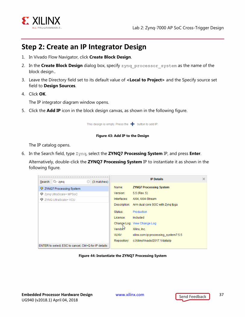
6. In the Search field, type Zynq, select the ZYNQ7 Processing System IP, and press Enter.
Alternatively, double-click the ZYNQ7 Processing System IP to instantiate it as shown in the
following figure.
Figure 44: Instantiate the ZYNQ7 Processing System
Send Feedback

Lab 2: Zynq-7000 AP SoC Cross-Trigger Design
Embedded Processor Hardware Design www.xilinx.com 38 UG940 (v2018.1) April 04, 2018
7. In the block design banner, click Run Block Automation as shown in the following figure.
Figure 45: Run Block Automation on Zynq Processing System
The Run Block Automation dialog box states that the FIXED_IO and the DDR pins on the ZYNQ7
Processing System 7 IP will be connected to external interface ports. Also, because you chose the
ZC702 board as your target board, the Apply Board Preset checkbox is checked by default.
8. Enable the Cross Trigger In and Cross Trigger Out functionality by setting those fields to Enable,
then click OK, as shown in the following figure:
Figure 46: Run Block Automation Dialog Box
Send Feedback

Lab 2: Zynq-7000 AP SoC Cross-Trigger Design
Embedded Processor Hardware Design www.xilinx.com 39 UG940 (v2018.1) April 04, 2018
This enables the TRIGGER_IN_0 and TRIGGER_OUT_0 interfaces in the ZYNQ7 Processing System
as show in the following figure.
Figure 47: IP Integrator Canvas After Running Block Automation
9. Add the AXI GPIO and AXI BRAM Controller to the design by right-clicking anywhere in the diagram
and selecting Add IP.
The diagram area looks like the following figure:
Figure 48: Diagram after Instantiating IP for This Design
10. Click the Run Connection Automation link at the top of the Diagram window.
The Run Connection Automation dialog box opens.
11. Select the All Automation (7 out of 7 selected) checkbox. This selects connection automation for all
the interfaces in the design. Select each automation to see the available options for that automation
in the right pane.
12. Make each of the following connections using the Run Connection Automation function.
Send Feedback

Lab 2: Zynq-7000 AP SoC Cross-Trigger Design
Embedded Processor Hardware Design www.xilinx.com 40 UG940 (v2018.1) April 04, 2018
Connection More Information Setting
axi_bram_ctrl_0
BRAM_PORTA
The Run Connection Automation dialog box
informs you that a new Block Memory Generator
IP will be instantiated and connected to the AXI
BRAM Controller PORTA.
No options.
axi_bram_ctrl_0
BRAM_PORTB
Note that the Run Connection Automation
dialog box offers two choices now. The first one
is to use the existing Block Memory Generator
from the previous step or you can chose to
instantiate a new Block Memory Generator if
desired.
In this case, use the existing BMG.
Leave the Blk_Mem_Gen
field set to its default
value of Blk_Mem_Gen of
BRAM_PORTA.
axi_bram_ctrl_0
S_AXI
The Run Connection Automation dialog box
states that the S_AXI port of the AXI BRAM
Controller will be connected to the M_AXI_GP0
port of the ZYNQ7 Processing System IP.
The AXI BRAM Controller needs to be connected
to a Block Memory Generator block. The
connection automation feature offers this
automation by instantiating the Block Memory
Generator IP and making appropriate
connections to the AXI BRAM Controller.
Leave the Clock
Connection (for
unconnected clks) field
set to Auto.
axi_gpio_0
GPIO
The Run Connection Automation dialog box
shows the interfaces that are available on the
ZC702 board to connect to the GPIO.
Select LEDs_4Bits.
axi_gpio_0
S_AXI
The Run Connection Automation dialog box
states that the S_AXI pin of the GPIO IP will be
connected to the M_AXI_GP0 pin of the ZYNQ7
Processing System. It also offers a choice for
different clock sources that might be relevant to
the design.
Leave the Clock
Connection (for
unconnected clks) field
set to Auto.
processing_system7_0
TRIGGER_IN_0
TRIGGER_OUT_0
The Run Connection Automation dialog box
states that the TRIGGER_IN_0 and
TRIGGER_OUT_0 pins will be connected to the
respective cross-trigger pins on the System ILA
IP.
Leave the ILA option to
its default value of Auto
for both TRIGGER_IN_0
and TRIGGER_OUT_0
option.
Send Feedback
Lab 2: Zynq-7000 AP SoC Cross-Trigger Design
Embedded Processor Hardware Design www.xilinx.com 41 UG940 (v2018.1) April 04, 2018
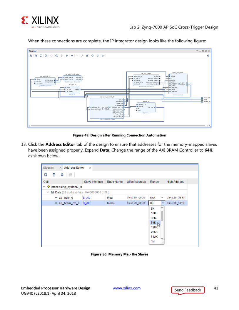
When these connections are complete, the IP integrator design looks like the following figure:
Figure 49: Design after Running Connection Automation
13. Click the Address Editor tab of the design to ensure that addresses for the memory-mapped slaves
have been assigned properly. Expand Data. Change the range of the AXI BRAM Controller to 64K,
as shown below.
Figure 50: Memory Map the Slaves
Send Feedback
Lab 2: Zynq-7000 AP SoC Cross-Trigger Design
Embedded Processor Hardware Design www.xilinx.com 42 UG940 (v2018.1) April 04, 2018
Mark Nets for Debugging
Next, you mark some nets for debugging.
1. Click the Diagram tab again and select the net connecting the GPIO pin of the AXI GPIO IP to the
LEDs_4Bits port.
2. Right-click in the block diagram area and select Debug. This marks the net for debug.
3. Notice that a bug symbol appears on the net to be debugged. You can also see this bug symbol in
the Design Hierarchy window on the selected net.
4. Similarly, select the net connecting the interface pin S_AXI of axi_gpio_0 and the M00_AXI
interface pin of ps7_0_axi_periph.
5. Right-click in the block design and select Debug from the context menu.
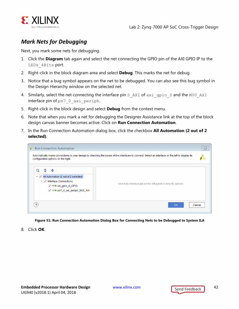
6. Note that when you mark a net for debugging the Designer Assistance link at the top of the block
design canvas banner becomes active. Click on Run Connection Automation.
7. In the Run Connection Automation dialog box, click the checkbox All Automation (2 out of 2
selected).
Figure 51: Run Connection Automation Dialog Box for Connecting Nets to be Debugged to System ILA
8. Click OK.
Send Feedback
Lab 2: Zynq-7000 AP SoC Cross-Trigger Design
Embedded Processor Hardware Design www.xilinx.com 43 UG940 (v2018.1) April 04, 2018
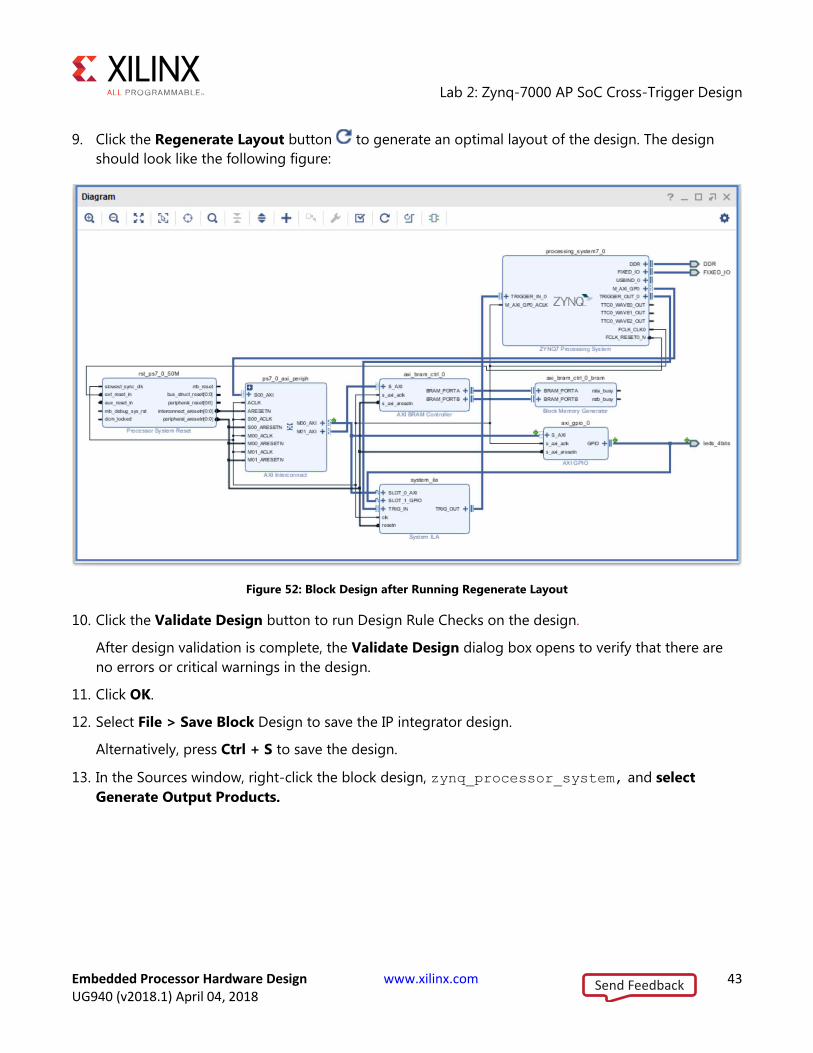
9. Click the Regenerate Layout button to generate an optimal layout of the design. The design
should look like the following figure:
Figure 52: Block Design after Running Regenerate Layout
10. Click the Validate Design button to run Design Rule Checks on the design.
After design validation is complete, the Validate Design dialog box opens to verify that there are
no errors or critical warnings in the design.
11. Click OK.
12. Select File > Save Block Design to save the IP integrator design.
Alternatively, press Ctrl + S to save the design.
13. In the Sources window, right-click the block design, zynq_processor_system, and select
Generate Output Products.
Send Feedback

Lab 2: Zynq-7000 AP SoC Cross-Trigger Design
Embedded Processor Hardware Design www.xilinx.com 44 UG940 (v2018.1) April 04, 2018
The Generate Output Products dialog box opens.
Figure 53: Generate Output Products Dialog Box
14. Click Generate.
15. The Generate Output Products dialog box informs you that out-of-context (OOC) module runs were
launched. Click OK on the Generate Output Products dialog box.
16. Wait until all OOC Module runs have finished running. This could take a few minutes.
Send Feedback

Lab 2: Zynq-7000 AP SoC Cross-Trigger Design
Embedded Processor Hardware Design www.xilinx.com 45 UG940 (v2018.1) April 04, 2018
Figure 54: Design Runs window showing the status of Out-of-Context Module Runs
17. In the Sources window, right-click zynq_processor_system, and select Create HDL Wrapper.
The Create HDL Wrapper dialog box offers two choices:
o The first choice is to generate a wrapper file that you can edit.
o The second choice is let Vivado generate and manage the wrapper file, meaning it is a read-
only file.
18. Keep the default setting, shown in the following figure, and click OK.
Figure 55: Create HDL Wrapper Dialog Box
Send Feedback
Lab 2: Zynq-7000 AP SoC Cross-Trigger Design
Embedded Processor Hardware Design www.xilinx.com 46 UG940 (v2018.1) April 04, 2018
Step 3: Implement Design and Generate Bitstream Now that the cross-trigger signals have been connected to the ILA for monitoring, you can complete
the rest of the flow.
1. Click Generate Bitstream to generate the bitstream for the design. The No Implementation
Results Available dialog box opens with a message asking whether its okay to launch synthesis and
implementation.
2. Click Yes.
3. The Launch Runs dialog box opens. Make the appropriate selections and click OK.
When bitstream generation completes, the Bitstream Generation Completed dialog box opens,
with the option Open Implemented Design option checked by default.
4. Click OK to open the implemented design.
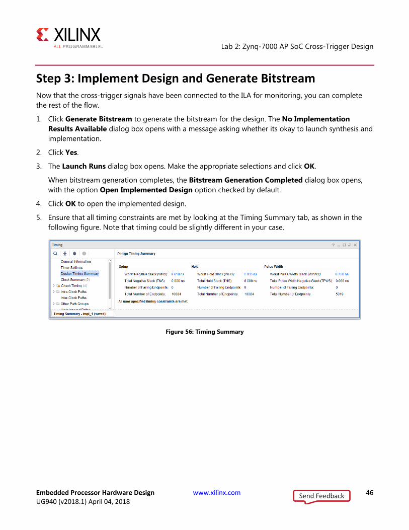
5. Ensure that all timing constraints are met by looking at the Timing Summary tab, as shown in the
following figure. Note that timing could be slightly different in your case.
Figure 56: Timing Summary
Send Feedback

Lab 2: Zynq-7000 AP SoC Cross-Trigger Design
Embedded Processor Hardware Design www.xilinx.com 47 UG940 (v2018.1) April 04, 2018
Step 4: Export Hardware to SDK After you generate the bitstream, you must export the hardware to SDK and generate your software
application.
1. Select File > Export > Export Hardware.
2. In the Export Hardware for SDK dialog box, make sure that the Include bitstream check box is
checked, and Export to field is set to <Local to Project>, as shown in the following figure.
Figure 57: Export Hardware for SDK Dialog Box
3. Click OK.
4. Select File > Launch SDK. Make sure that both the Exported location and Workspace fields are
set to <Local to Project>, as shown below in the following figure:
Figure 58: Launch SDK Dialog Box
5. Click OK.
Send Feedback
Lab 2: Zynq-7000 AP SoC Cross-Trigger Design
Embedded Processor Hardware Design www.xilinx.com 48 UG940 (v2018.1) April 04, 2018
Step 5: Build Application Code in SDK SDK launches in a separate window.
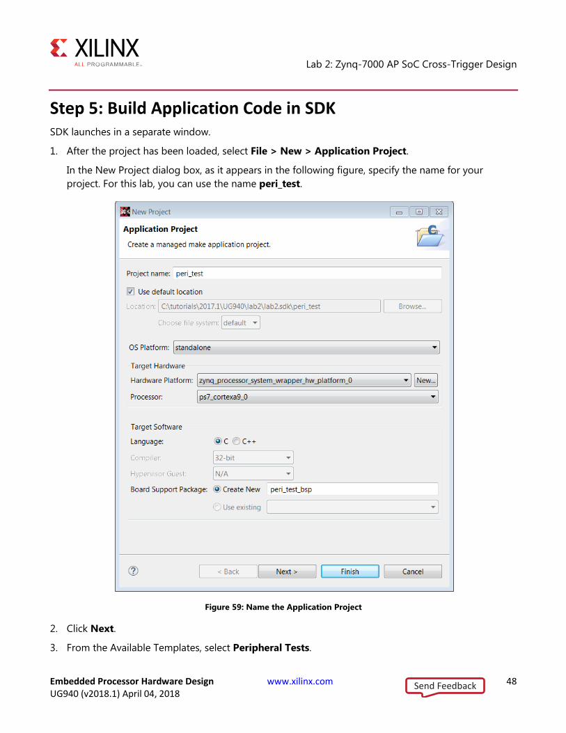
1. After the project has been loaded, select File > New > Application Project.
In the New Project dialog box, as it appears in the following figure, specify the name for your
project. For this lab, you can use the name peri_test.
Figure 59: Name the Application Project
2. Click Next.
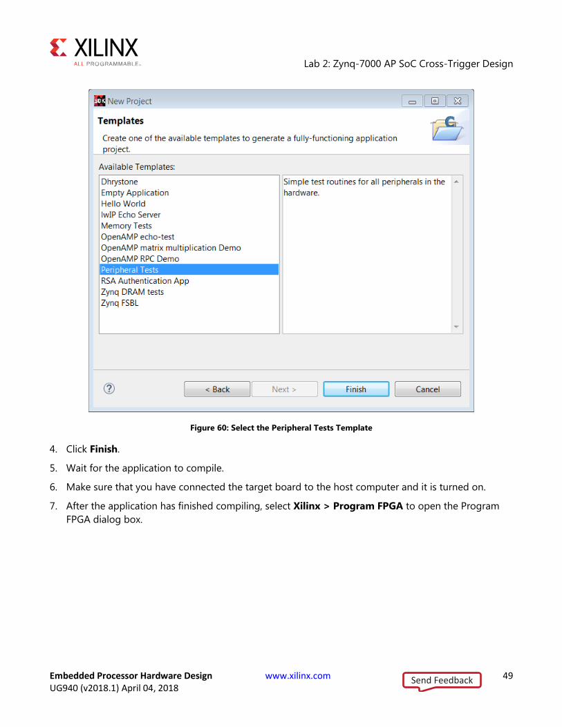
3. From the Available Templates, select Peripheral Tests.
Send Feedback
Lab 2: Zynq-7000 AP SoC Cross-Trigger Design
Embedded Processor Hardware Design www.xilinx.com 49 UG940 (v2018.1) April 04, 2018
Figure 60: Select the Peripheral Tests Template
4. Click Finish.
5. Wait for the application to compile.
6. Make sure that you have connected the target board to the host computer and it is turned on.
7. After the application has finished compiling, select Xilinx > Program FPGA to open the Program
FPGA dialog box.
Send Feedback

Lab 2: Zynq-7000 AP SoC Cross-Trigger Design
Embedded Processor Hardware Design www.xilinx.com 50 UG940 (v2018.1) April 04, 2018
8. In the Program FPGA dialog box, click Program.
Figure 61: Program FPGA Dialog Box
9. Select and right-click the peri_test application in the Project Explorer, and select Debug As >
Debug Configurations.
The Debug Configurations dialog box opens.
Send Feedback
Lab 2: Zynq-7000 AP SoC Cross-Trigger Design
Embedded Processor Hardware Design www.xilinx.com 51 UG940 (v2018.1) April 04, 2018
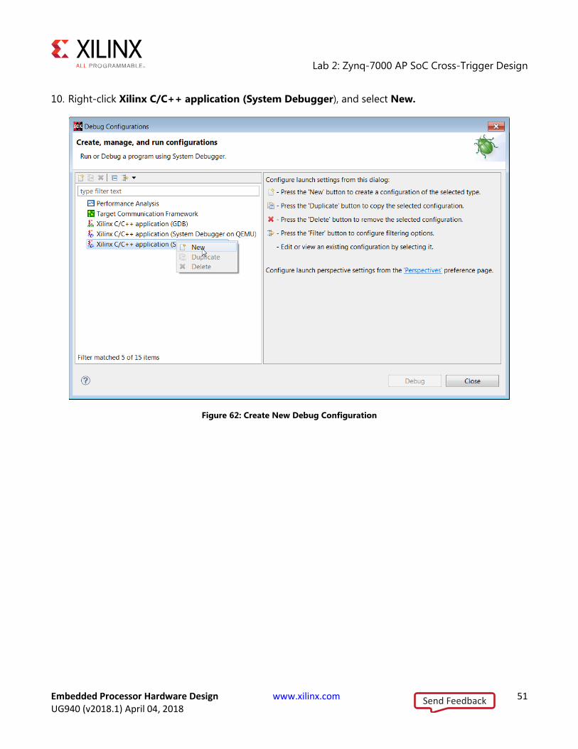
10. Right-click Xilinx C/C++ application (System Debugger), and select New.
Figure 62: Create New Debug Configuration
Send Feedback
Lab 2: Zynq-7000 AP SoC Cross-Trigger Design
Embedded Processor Hardware Design www.xilinx.com 52 UG940 (v2018.1) April 04, 2018
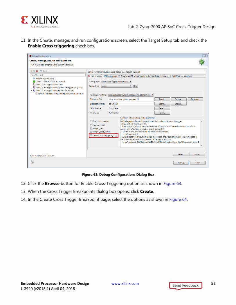
11. In the Create, manage, and run configurations screen, select the Target Setup tab and check the
Enable Cross triggering check box.
Figure 63: Debug Configurations Dialog Box
12. Click the Browse button for Enable Cross-Triggering option as shown in Figure 63.
13. When the Cross Trigger Breakpoints dialog box opens, click Create.
14. In the Create Cross Trigger Breakpoint page, select the options as shown in Figure 64.
Send Feedback

Lab 2: Zynq-7000 AP SoC Cross-Trigger Design
Embedded Processor Hardware Design www.xilinx.com 53 UG940 (v2018.1) April 04, 2018
Figure 64: Setting Cross-Trigger Breakpoints for Processor to Fabric Trigger
15. Click OK. This sets up the cross trigger condition for Processor to Fabric.
16. In the Cross Trigger Breakpoints dialog box click Create again, as shown in the following figure:
Figure 65: Setting Breakpoints for Cross-Triggering Between Fabric and Processor
Send Feedback

Lab 2: Zynq-7000 AP SoC Cross-Trigger Design
Embedded Processor Hardware Design www.xilinx.com 54 UG940 (v2018.1) April 04, 2018
17. In the Create Cross Trigger Breakpoint page, select the options as shown in the following figure:
Figure 66: Setting Cross-Trigger Breakpoints for Processor to Fabric Trigger
18. Click OK. This sets up the cross trigger condition for Fabric to Processor.
19. In the Cross Trigger Breakpoints dialog box click OK.
Figure 67: Cross Trigger Breakpoints Dialog Box showing the Selection for Breakpoint
Send Feedback

Lab 2: Zynq-7000 AP SoC Cross-Trigger Design
Embedded Processor Hardware Design www.xilinx.com 55 UG940 (v2018.1) April 04, 2018
20. In the Debug Configurations dialog box, click Debug, as shown at the bottom of the following
figure.
Figure 68: Debug Configurations dialog box after setting breakpoints
The Confirm Perspective Switch dialog box opens.
21. Click Yes to confirm the perspective switch.
The Debug perspective window opens.
22. Set the terminal by selecting the SDK Terminal tab and clicking the icon.
Send Feedback

Lab 2: Zynq-7000 AP SoC Cross-Trigger Design
Embedded Processor Hardware Design www.xilinx.com 56 UG940 (v2018.1) April 04, 2018
23. Use the following settings in the following figure for the ZC702 board, and click OK.
Figure 69: Terminal Settings
24. Verify the Terminal connection by checking the status at the top of the tab as shown in the
following figure.
Figure 70: Verify Terminal Connection
25. If it is not already open, select ../src/testperiph.c, and double click to open the source file.
Send Feedback
Lab 2: Zynq-7000 AP SoC Cross-Trigger Design
Embedded Processor Hardware Design www.xilinx.com 57 UG940 (v2018.1) April 04, 2018
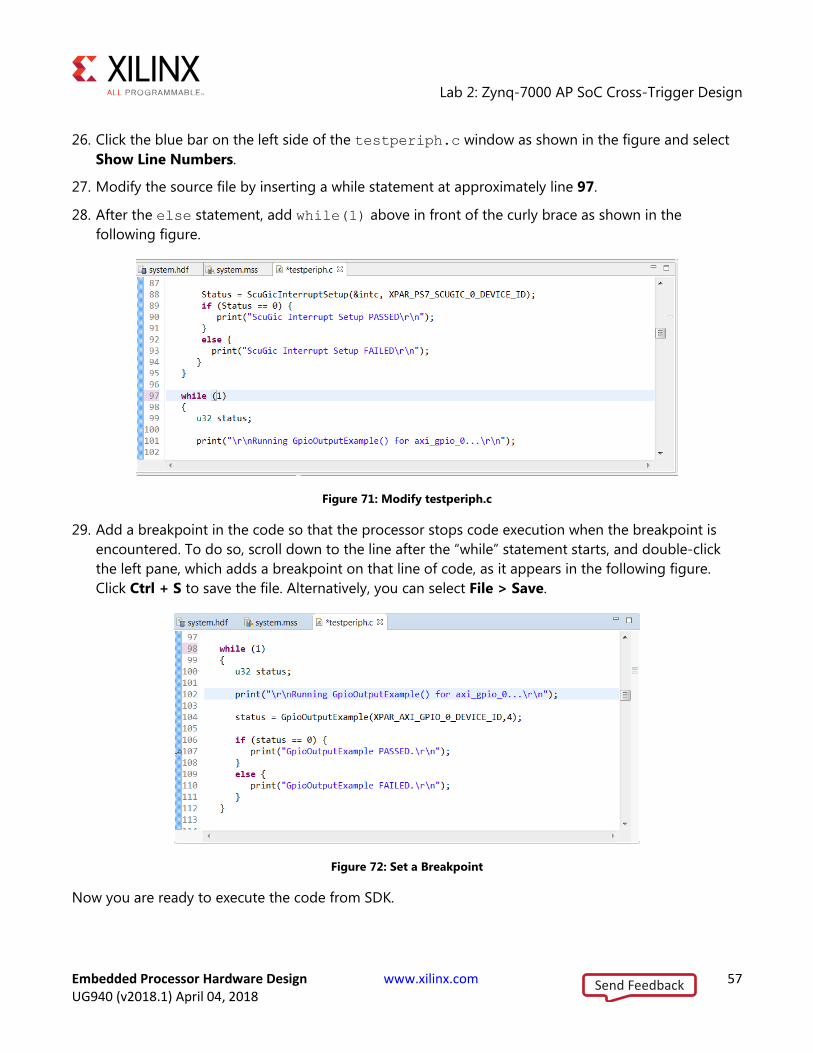
26. Click the blue bar on the left side of the testperiph.c window as shown in the figure and select
Show Line Numbers.
27. Modify the source file by inserting a while statement at approximately line 97.
28. After the else statement, add while(1) above in front of the curly brace as shown in the
following figure.
Figure 71: Modify testperiph.c
29. Add a breakpoint in the code so that the processor stops code execution when the breakpoint is
encountered. To do so, scroll down to the line after the “while” statement starts, and double-click
the left pane, which adds a breakpoint on that line of code, as it appears in the following figure.
Click Ctrl + S to save the file. Alternatively, you can select File > Save.
Figure 72: Set a Breakpoint
Now you are ready to execute the code from SDK.
Send Feedback

Lab 2: Zynq-7000 AP SoC Cross-Trigger Design
Embedded Processor Hardware Design www.xilinx.com 58 UG940 (v2018.1) April 04, 2018
Step 6: Connect to Vivado Logic Analyzer Connect to the ZC702 board using the Vivado Logic Analyzer.
1. In the Vivado IDE session, from the Program and Debug drop-down list of the Vivado Flow
Navigator, select Open Hardware Manager.
2. In the Hardware Manager window, click Open target > Open New Target.
Figure 73: Open a New Hardware Target
Note: You can also use the Auto Connect option to connect to the target hardware.
The Open New Hardware Target dialog box opens, shown in the following figure.
Figure 74: Open Hardware Target
3. Click Next.
Send Feedback
Lab 2: Zynq-7000 AP SoC Cross-Trigger Design
Embedded Processor Hardware Design www.xilinx.com 59 UG940 (v2018.1) April 04, 2018
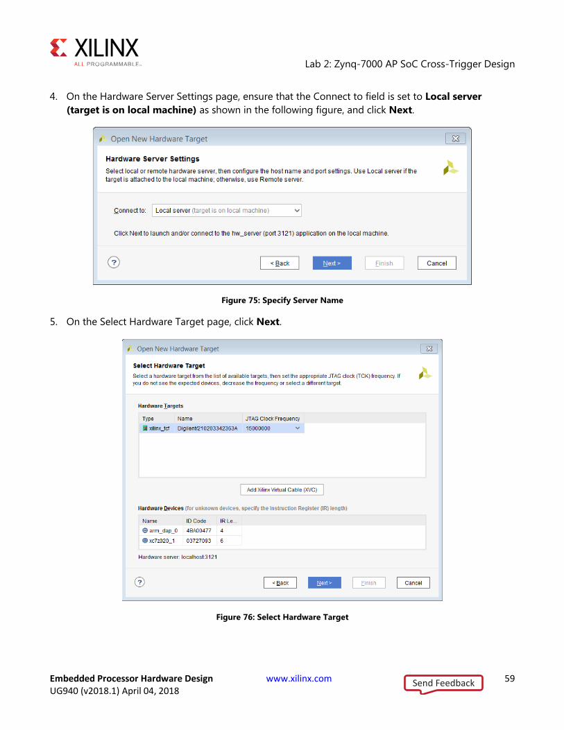
4. On the Hardware Server Settings page, ensure that the Connect to field is set to Local server
(target is on local machine) as shown in the following figure, and click Next.
Figure 75: Specify Server Name
5. On the Select Hardware Target page, click Next.
Figure 76: Select Hardware Target
Send Feedback
Lab 2: Zynq-7000 AP SoC Cross-Trigger Design
Embedded Processor Hardware Design www.xilinx.com 60 UG940 (v2018.1) April 04, 2018
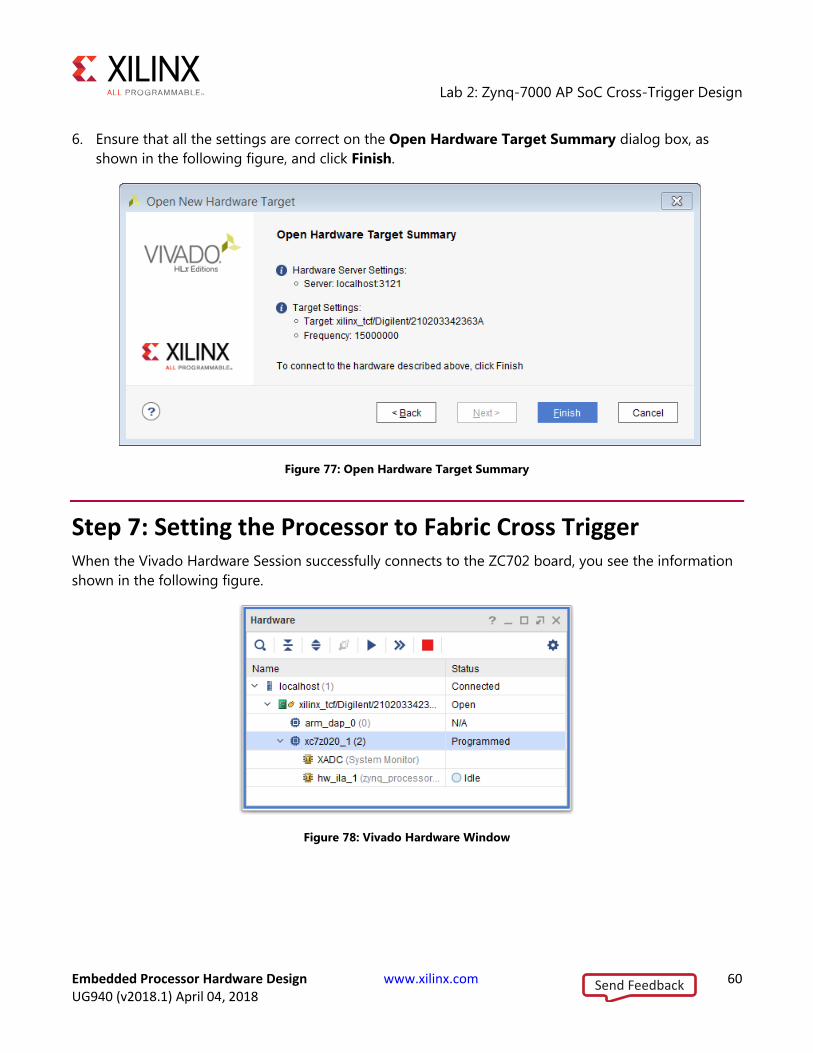
6. Ensure that all the settings are correct on the Open Hardware Target Summary dialog box, as
shown in the following figure, and click Finish.
Figure 77: Open Hardware Target Summary
Step 7: Setting the Processor to Fabric Cross Trigger When the Vivado Hardware Session successfully connects to the ZC702 board, you see the information
shown in the following figure.
Figure 78: Vivado Hardware Window
Send Feedback
Lab 2: Zynq-7000 AP SoC Cross-Trigger Design
Embedded Processor Hardware Design www.xilinx.com 61 UG940 (v2018.1) April 04, 2018
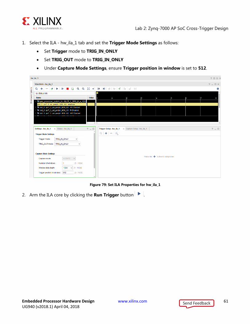
1. Select the ILA - hw_ila_1 tab and set the Trigger Mode Settings as follows:
Set Trigger mode to TRIG_IN_ONLY
Set TRIG_OUT mode to TRIG_IN_ONLY
Under Capture Mode Settings, ensure Trigger position in window is set to 512.
Figure 79: Set ILA Properties for hw_ila_1
2. Arm the ILA core by clicking the Run Trigger button .
Send Feedback
Lab 2: Zynq-7000 AP SoC Cross-Trigger Design
Embedded Processor Hardware Design www.xilinx.com 62 UG940 (v2018.1) April 04, 2018
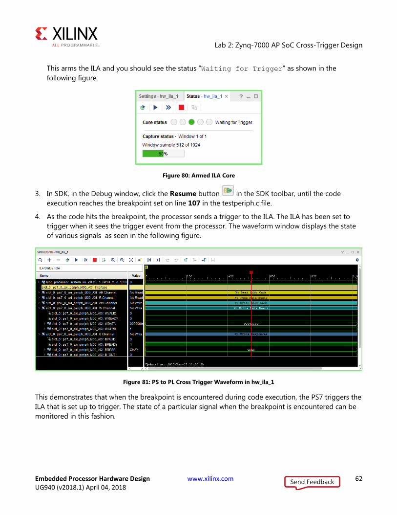
This arms the ILA and you should see the status “Waiting for Trigger” as shown in the
following figure.
Figure 80: Armed ILA Core
3. In SDK, in the Debug window, click the Resume button in the SDK toolbar, until the code
execution reaches the breakpoint set on line 107 in the testperiph.c file.
4. As the code hits the breakpoint, the processor sends a trigger to the ILA. The ILA has been set to
trigger when it sees the trigger event from the processor. The waveform window displays the state
of various signals as seen in the following figure.
Figure 81: PS to PL Cross Trigger Waveform in hw_ila_1
This demonstrates that when the breakpoint is encountered during code execution, the PS7 triggers the
ILA that is set up to trigger. The state of a particular signal when the breakpoint is encountered can be
monitored in this fashion.
Send Feedback

Lab 2: Zynq-7000 AP SoC Cross-Trigger Design
Embedded Processor Hardware Design www.xilinx.com 63 UG940 (v2018.1) April 04, 2018
Step 8: Setting the Fabric to Processor Cross-Trigger Now try the fabric to processor side of the cross-trigger mechanism. To do this remove the breakpoint
that you set earlier on line 107 to have the ILA trigger the processor and stop code execution.
1. In SDK, select the Breakpoints tab towards the top right corner of SDK window, right-click it, and
uncheck the testperiph.c [line: 106] checkbox. This removes the breakpoint that you set up earlier.
Note: Alternatively, you can select the breakpoint in line 107 of the testperiph.c file, right click
and select Disable Breakpoint.
2. In the Debug window, click Resume icon on the SDK toolbar. The code runs continuously because it
has an infinite loop.
You can see the code executing in the Terminal Window in SDK.
3. In Vivado, select the Settings – hw_ila_1 tab. Change the Trigger Mode to BASIC_OR_TRIG_IN and
the TRIG_OUT mode to TRIGGER_OR_TRIG_IN.
4. Click on the + sign in the Trigger Setup window to add the
slot_0:ps7_0_axi_periph_M00_AXI:AWVALID signal from the Add Probes window.
5. In the Basic Trigger Setup window, ensure that the Radix is set to [B] Binary and change the Value
for the slot_0:ps7_0_axi_periph_M00_AXI:AWVALID signal to 1. This essentially sets up the
ILA to trigger when the awvalid transitions to a value of 1.
6. Click the Run Trigger button to “arm” the ILA. It triggers immediately as the SDK code is
running AXI transactions which causes the awvalid signal to toggle. This causes the trigger_out of
the ILA to toggle which eventually will halt the processor from executing the code.
This is seen in SDK the in the highlighted area of the debug window.
Figure 82: Verify that the Processor Has Been Interrupted in SDK
Send Feedback

Lab 2: Zynq-7000 AP SoC Cross-Trigger Design
Embedded Processor Hardware Design www.xilinx.com 64 UG940 (v2018.1) April 04, 2018
Conclusion This lab demonstrated how cross triggering works in a Zynq-7000 AP SoC processor based design. You
can use cross triggering to co-debug hardware and software in an integrated environment.
Lab Files This tutorial demonstrates the cross-trigger feature of the Zynq-7000 AP SoC processor, which you
perform in the GUI environment. Therefore, the only Tcl file provided is lab2.tcl.
The lab2.tcl file helps you run all the steps all the way to exporting hardware for SDK.
The debug portion of the lab must be carried out in the GUI; no Tcl files are provided for that purpose.
Send Feedback
Embedded Processor Hardware Design www.xilinx.com 65 UG940 (v2018.1) April 04, 2018
Lab 3: Using the Embedded MicroBlaze Processor
Introduction In this tutorial, you create a simple MicroBlaze™ system for a Kintex®-7 FPGA using Vivado® IP
integrator.
The MicroBlaze system includes native Xilinx® IP including:
MicroBlaze processor
AXI block RAM
Double Data Rate 3 (DDR3) memory
UARTLite
GPIO
Debug Module (MDM)
Proc Sys Reset
Local memory bus (LMB)
Parts of the block design are constructed using the Platform Board Flow feature.
This lab also shows the cross-trigger capability of the MicroBlaze processor.
The feature is demonstrated using a software application code developed in SDK in a stand-alone
application mode.
This lab targets the Xilinx KC705 FPGA Evaluation Board.
Send Feedback
Lab 3: Using the Embedded MicroBlaze Processor
Embedded Processor Hardware Design www.xilinx.com 66 UG940 (v2018.1) April 04, 2018
Step 1: Invoke the Vivado IDE and Create a Project 1. Open the Vivado IDE by clicking the desktop icon or by typing vivado at a terminal command line.
2. From the Quick Start page, select Create Project.
The New Project wizard opens. Click Next.
3. In the Project Name dialog box, type the project name and location. Make sure that Create project
subdirectory is checked. Click Next.
4. In the Project Type dialog box, select RTL Project. Click Next.
5. In the Add Sources dialog box, ensure that the Target language is set to VHDL or Verilog. Set the
Simulator language to Mixed.
6. Click Next.
7. In Add Constraints dialog box, click Next.
8. In the Default Part dialog box, select Boards and choose the Kintex-7 KC705 Evaluation Platform
along with the correct version. Click Next.
9. Review the project summary in the New Project Summary dialog box before clicking Finish to
create the project.
Because you selected the KC705 board when you created the Vivado IDE project, you see the
following message in the Tcl Console:
set_property board part xilinx.com:kc705:part0:1.5 [current_project]
Although Tcl commands are available for many of the actions performed in the Vivado IDE, they are not
explained in this tutorial. Instead, a Tcl script is provided that can be used to recreate this entire project.
See the Tcl Console for more information. You can also refer to the Vivado Design Suit Tcl Command
Reference Guide (UG835) for information about the write_bd_tcl commands.
Send Feedback
Lab 3: Using the Embedded MicroBlaze Processor
Embedded Processor Hardware Design www.xilinx.com 67 UG940 (v2018.1) April 04, 2018
Step 2: Create an IP Integrator Design 1. From Flow Navigator, under IP integrator, select Create Block Design.
The Create Block Design dialog box opens.
2. Specify the IP subsystem design name. For this step, you can use mb_subsystem as the Design
name. Leave the Directory field set to its default value of <Local to Project>. Leave the Specify
source set drop-down list set to its default value of Design Sources.
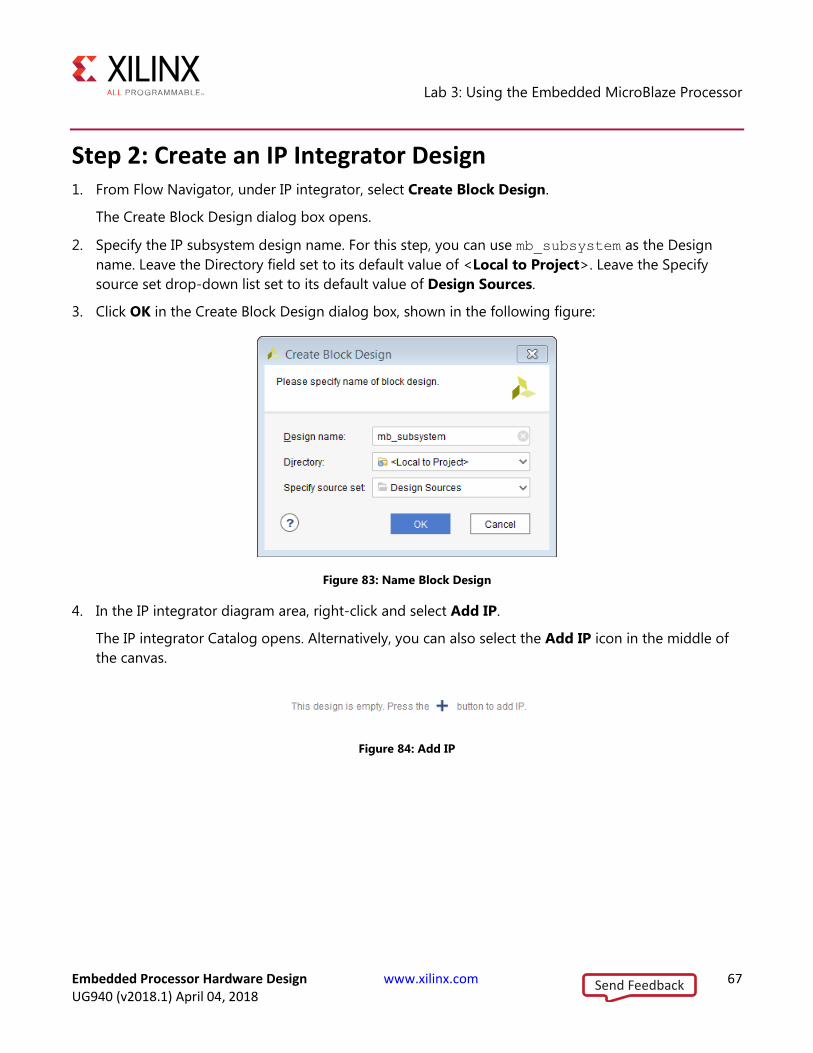
3. Click OK in the Create Block Design dialog box, shown in the following figure:
Figure 83: Name Block Design
4. In the IP integrator diagram area, right-click and select Add IP.
The IP integrator Catalog opens. Alternatively, you can also select the Add IP icon in the middle of
the canvas.
Figure 84: Add IP
Send Feedback
Lab 3: Using the Embedded MicroBlaze Processor
Embedded Processor Hardware Design www.xilinx.com 68 UG940 (v2018.1) April 04, 2018
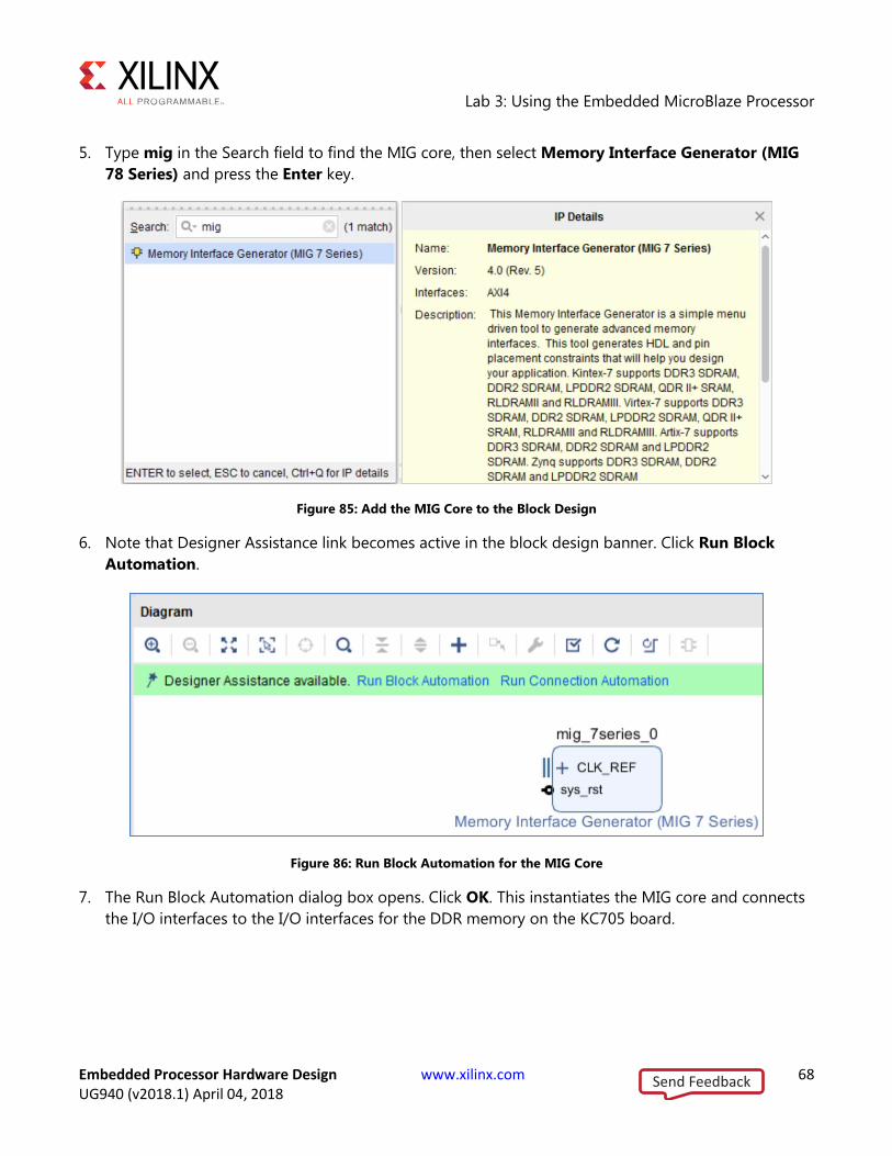
5. Type mig in the Search field to find the MIG core, then select Memory Interface Generator (MIG
78 Series) and press the Enter key.
Figure 85: Add the MIG Core to the Block Design
6. Note that Designer Assistance link becomes active in the block design banner. Click Run Block
Automation.
Figure 86: Run Block Automation for the MIG Core
7. The Run Block Automation dialog box opens. Click OK. This instantiates the MIG core and connects
the I/O interfaces to the I/O interfaces for the DDR memory on the KC705 board.
Send Feedback
Lab 3: Using the Embedded MicroBlaze Processor
Embedded Processor Hardware Design www.xilinx.com 69 UG940 (v2018.1) April 04, 2018
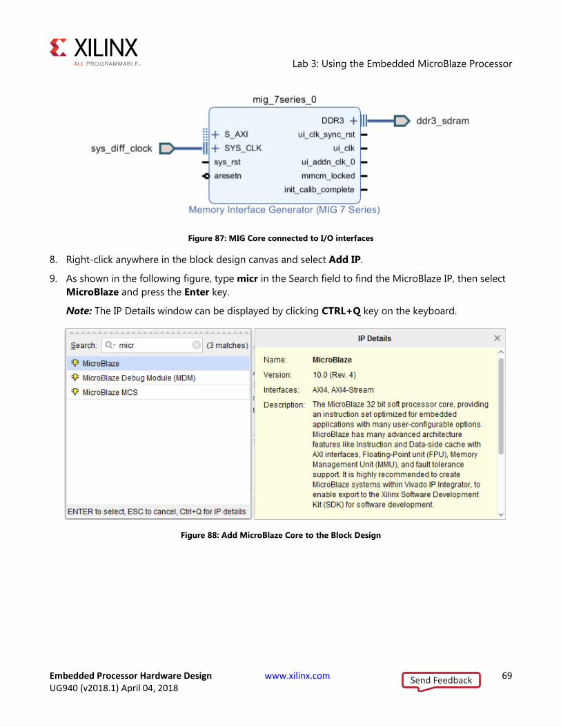
Figure 87: MIG Core connected to I/O interfaces
8. Right-click anywhere in the block design canvas and select Add IP.
9. As shown in the following figure, type micr in the Search field to find the MicroBlaze IP, then select
MicroBlaze and press the Enter key.
Note: The IP Details window can be displayed by clicking CTRL+Q key on the keyboard.
Figure 88: Add MicroBlaze Core to the Block Design
Send Feedback

Lab 3: Using the Embedded MicroBlaze Processor
Embedded Processor Hardware Design www.xilinx.com 70 UG940 (v2018.1) April 04, 2018
Use the Board Tab to Connect to Board Interfaces
There are several ways to use an existing interface in IP Integrator. Use the Board tab to instantiate
some of the interfaces that are present on the KC705 board.
1. Select the Board tab to see the interfaces present on the KC705 board.
Figure 89: Board Tab for KC705 board
Send Feedback
Lab 3: Using the Embedded MicroBlaze Processor
Embedded Processor Hardware Design www.xilinx.com 71 UG940 (v2018.1) April 04, 2018
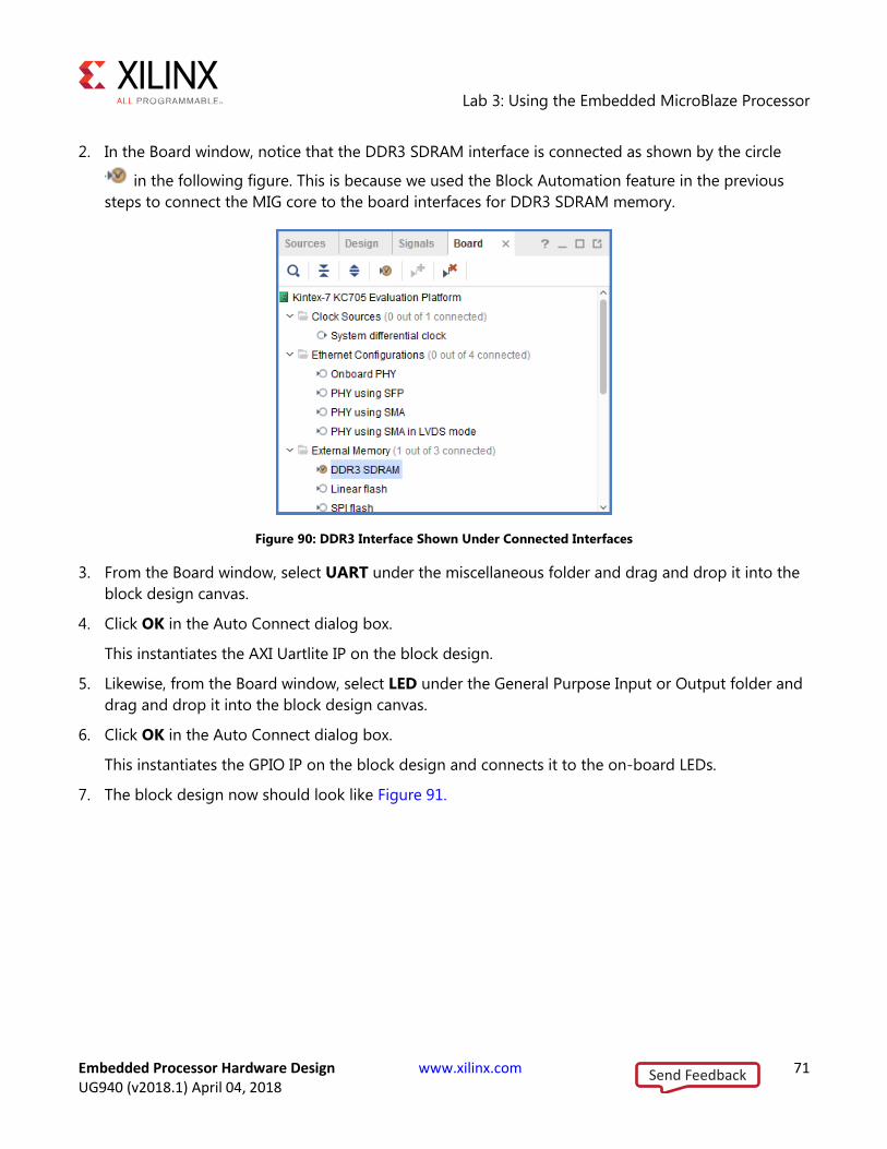
2. In the Board window, notice that the DDR3 SDRAM interface is connected as shown by the circle
in the following figure. This is because we used the Block Automation feature in the previous
steps to connect the MIG core to the board interfaces for DDR3 SDRAM memory.
Figure 90: DDR3 Interface Shown Under Connected Interfaces
3. From the Board window, select UART under the miscellaneous folder and drag and drop it into the
block design canvas.
4. Click OK in the Auto Connect dialog box.
This instantiates the AXI Uartlite IP on the block design.
5. Likewise, from the Board window, select LED under the General Purpose Input or Output folder and
drag and drop it into the block design canvas.
6. Click OK in the Auto Connect dialog box.
This instantiates the GPIO IP on the block design and connects it to the on-board LEDs.
7. The block design now should look like Figure 91.
Send Feedback

Lab 3: Using the Embedded MicroBlaze Processor
Embedded Processor Hardware Design www.xilinx.com 72 UG940 (v2018.1) April 04, 2018
Figure 91: Block Design After Connecting the rs232_uart and the led_8bits Interfaces
Add Peripheral: AXI BRAM Controller
1. Add the AXI BRAM Controller, shown in the following figure, by right-clicking the IPI canvas and
selecting Add IP.
Figure 92: Add BRAM Controller
Send Feedback

Lab 3: Using the Embedded MicroBlaze Processor
Embedded Processor Hardware Design www.xilinx.com 73 UG940 (v2018.1) April 04, 2018
Run Block Automation
1. Click Run Block Automation, displayed in the following figure:
Figure 93: Run Block Automation
The Run Block Automation dialog box opens, as shown in the following figure.
The values of the fields shown in this figure show the values that you will set in the next step.
Figure 94: Run Block Automation Dialog Box
Send Feedback

Lab 3: Using the Embedded MicroBlaze Processor
Embedded Processor Hardware Design www.xilinx.com 74 UG940 (v2018.1) April 04, 2018
2. On the Run Block Automation page:
a. Leave Preset to its default value of None.
b. Set Local Memory to 64 KB.
c. Leave the Local Memory ECC to its default value of None.
d. Change the Cache Configuration to 32 KB.
e. Change the Debug Module option to Extended Debug.
f. Leave the Peripheral AXI Port option set to its default value of Enabled.
g. Leave the Clock Connection option set to /mig_7series_0/ui_addn_clk_0 (100 MHz).
3. Click OK.
This generates a basic MicroBlaze system in the IP Integrator diagram area, shown in the following
figure.
Figure 95: MicroBlaze System
Send Feedback

Lab 3: Using the Embedded MicroBlaze Processor
Embedded Processor Hardware Design www.xilinx.com 75 UG940 (v2018.1) April 04, 2018
Use Connection Automation
Run Connection Automation provides several options that you can select to make connections. This
section will walk you through the first connection, and then you will use the same procedure to make
the rest of the required connections for this tutorial.
1. Click Run Connection Automation as shown in the following figure.
Figure 96: Run Connection Automation
The Run Connection Automation dialog box opens.
2. Check the interfaces in the left pane of the dialog box as shown in the following figure:
Figure 97: Run Connection Automation Dialog Box
3. Use the following table to set options in the Run Connection Automation dialog box.
Send Feedback
Lab 3: Using the Embedded MicroBlaze Processor
Embedded Processor Hardware Design www.xilinx.com 76 UG940 (v2018.1) April 04, 2018
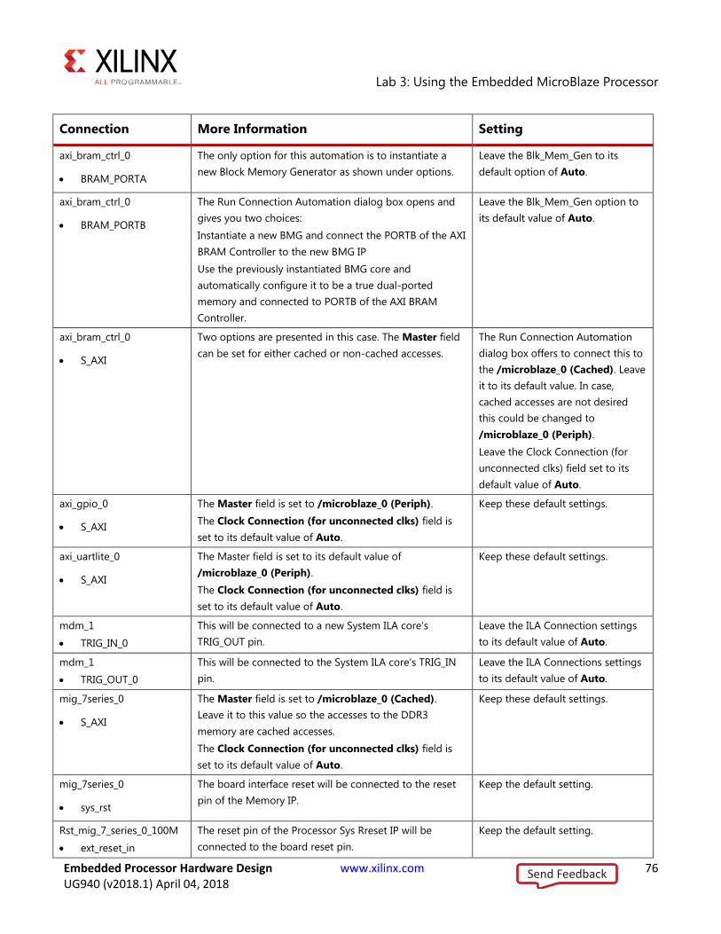
Connection More Information Setting
axi_bram_ctrl_0
BRAM_PORTA
The only option for this automation is to instantiate a
new Block Memory Generator as shown under options.
Leave the Blk_Mem_Gen to its
default option of Auto.
axi_bram_ctrl_0
BRAM_PORTB
The Run Connection Automation dialog box opens and
gives you two choices:
Instantiate a new BMG and connect the PORTB of the AXI
BRAM Controller to the new BMG IP
Use the previously instantiated BMG core and
automatically configure it to be a true dual-ported
memory and connected to PORTB of the AXI BRAM
Controller.
Leave the Blk_Mem_Gen option to
its default value of Auto.
axi_bram_ctrl_0
S_AXI
Two options are presented in this case. The Master field
can be set for either cached or non-cached accesses.
The Run Connection Automation
dialog box offers to connect this to
the /microblaze_0 (Cached). Leave
it to its default value. In case,
cached accesses are not desired
this could be changed to
/microblaze_0 (Periph).
Leave the Clock Connection (for
unconnected clks) field set to its
default value of Auto.
axi_gpio_0
S_AXI
The Master field is set to /microblaze_0 (Periph).
The Clock Connection (for unconnected clks) field is
set to its default value of Auto.
Keep these default settings.
axi_uartlite_0
S_AXI
The Master field is set to its default value of
/microblaze_0 (Periph).
The Clock Connection (for unconnected clks) field is
set to its default value of Auto.
Keep these default settings.
mdm_1
TRIG_IN_0
This will be connected to a new System ILA core’s
TRIG_OUT pin.
Leave the ILA Connection settings
to its default value of Auto.
mdm_1
TRIG_OUT_0
This will be connected to the System ILA core’s TRIG_IN
pin.
Leave the ILA Connections settings
to its default value of Auto.
mig_7series_0
S_AXI
The Master field is set to /microblaze_0 (Cached).
Leave it to this value so the accesses to the DDR3
memory are cached accesses.
The Clock Connection (for unconnected clks) field is
set to its default value of Auto.
Keep these default settings.
mig_7series_0
sys_rst
The board interface reset will be connected to the reset
pin of the Memory IP.
Keep the default setting.
Rst_mig_7_series_0_100M
ext_reset_in
The reset pin of the Processor Sys Rreset IP will be
connected to the board reset pin.
Keep the default setting.
Send Feedback

Lab 3: Using the Embedded MicroBlaze Processor
Embedded Processor Hardware Design www.xilinx.com 77 UG940 (v2018.1) April 04, 2018
4. After setting the appropriate options as shown in the table above, click OK.
At this point, your IP integrator diagram area should look like the following figure. The relative
placement of your IP might be slightly different.
Figure 98: MicroBlaze Connected to UART, GPIO and AXI BRAM Controller
Mark Nets for Debugging
1. To monitor the AXI transactions taking place between the MicroBlaze and the GPIO, select the
interface net connecting M01_AXI interface pin of the microblaze_0_axi_periph instance and
the S_AXI interface pin of the axi_gpio_0 instance.
2. Right-click and select Debug from the context menu.
Note: the Designer Assistance is available as indicated by the Run Connection Automation link
in the banner of the block design.
3. Click the Run Connection Automation link.
Send Feedback
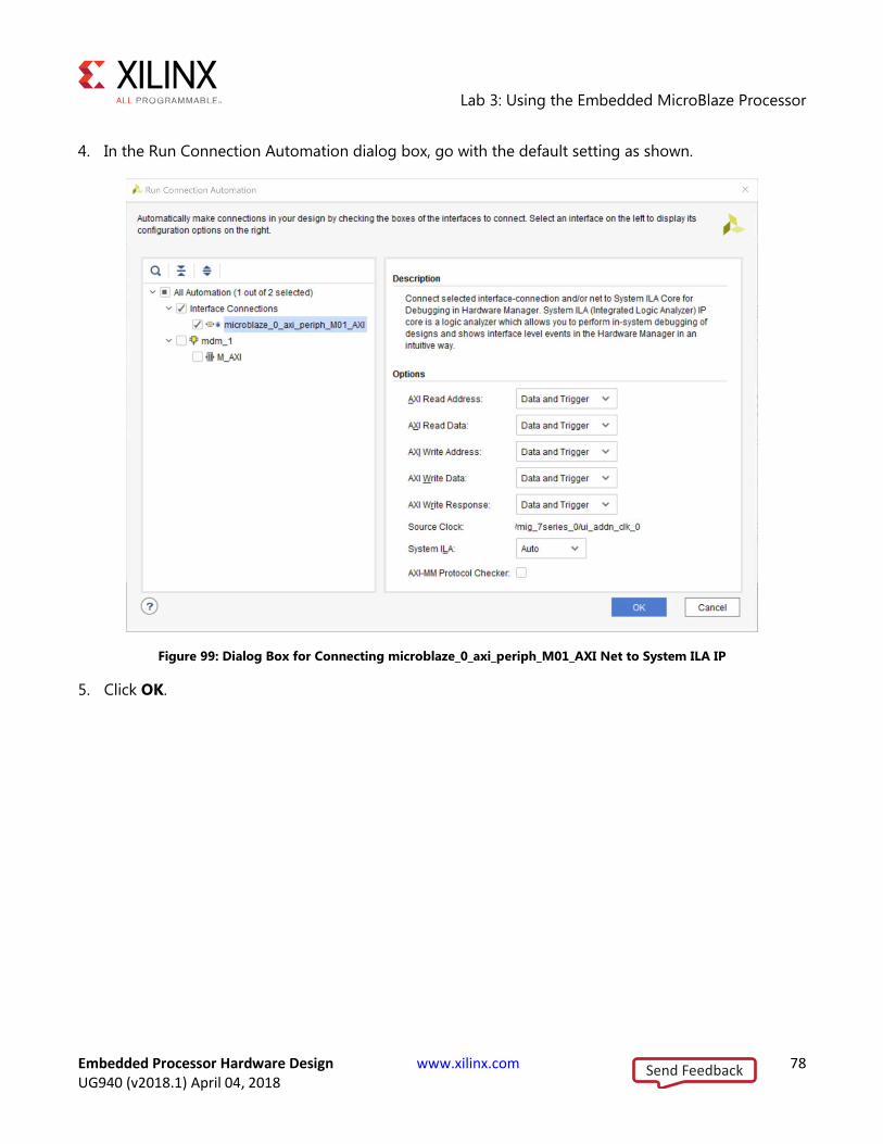
Lab 3: Using the Embedded MicroBlaze Processor
Embedded Processor Hardware Design www.xilinx.com 78 UG940 (v2018.1) April 04, 2018
4. In the Run Connection Automation dialog box, go with the default setting as shown.
Figure 99: Dialog Box for Connecting microblaze_0_axi_periph_M01_AXI Net to System ILA IP
5. Click OK.
Send Feedback
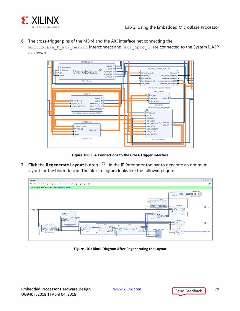
Lab 3: Using the Embedded MicroBlaze Processor
Embedded Processor Hardware Design www.xilinx.com 79 UG940 (v2018.1) April 04, 2018
6. The cross-trigger pins of the MDM and the AXI Interface net connecting the
microblaze_0_axi_periph Interconnect and axi_gpio_0 are connected to the System ILA IP
as shown.
Figure 100: ILA Connections to the Cross-Trigger Interface
7. Click the Regenerate Layout button in the IP Integrator toolbar to generate an optimum
layout for the block design. The block diagram looks like the following figure.
Figure 101: Block Diagram After Regenerating the Layout
Send Feedback
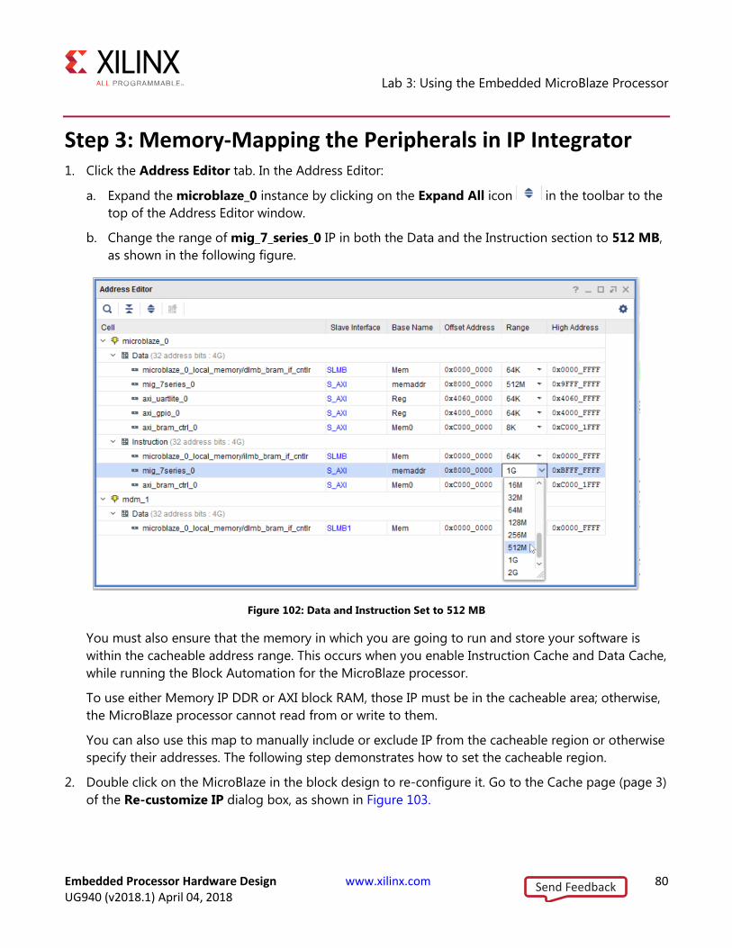
Lab 3: Using the Embedded MicroBlaze Processor
Embedded Processor Hardware Design www.xilinx.com 80 UG940 (v2018.1) April 04, 2018
Step 3: Memory-Mapping the Peripherals in IP Integrator 1. Click the Address Editor tab. In the Address Editor:
a. Expand the microblaze_0 instance by clicking on the Expand All icon in the toolbar to the
top of the Address Editor window.
b. Change the range of mig_7_series_0 IP in both the Data and the Instruction section to 512 MB,
as shown in the following figure.
Figure 102: Data and Instruction Set to 512 MB
You must also ensure that the memory in which you are going to run and store your software is
within the cacheable address range. This occurs when you enable Instruction Cache and Data Cache,
while running the Block Automation for the MicroBlaze processor.
To use either Memory IP DDR or AXI block RAM, those IP must be in the cacheable area; otherwise,
the MicroBlaze processor cannot read from or write to them.
You can also use this map to manually include or exclude IP from the cacheable region or otherwise
specify their addresses. The following step demonstrates how to set the cacheable region.
2. Double click on the MicroBlaze in the block design to re-configure it. Go to the Cache page (page 3)
of the Re-customize IP dialog box, as shown in Figure 103.
Send Feedback

Lab 3: Using the Embedded MicroBlaze Processor
Embedded Processor Hardware Design www.xilinx.com 81 UG940 (v2018.1) April 04, 2018
On this page, for both the Instruction Cache and Data Cache:
a. The Size in Bytes option should be set to 32 kB. Leave it set to this value.
b. Set the Line length option to 8.
3. Set the Base Address to 0x80000000 by clicking the checkbox so that it changes to manual mode,
which enables the Base Address field.
4. Set the High Address to 0x9FFFFFFF by clicking the checkbox so that it changes to manual mode,
which enables the High Address field.
5. Enable Use Cache for All Memory Accesses for both caches by clicking the checkbox first to
change it to Manual Mode, and then checking the check box.
6. Next, verify that the size of the cacheable segment of memory (that is, the memory space between
the Base and High addresses of the Instruction Cache and Data Cache) is a power of 2, which it
should be if the options were set as specified. Additionally, ensure that the Base address and the
High address of both Data Cache and Instruction Cache are the same.
7. Ensure that all IP that are slaves of the Instruction Cache, and that the Data Cache buses fall within
this cacheable segment. Otherwise, the MicroBlaze processor cannot access those IP.
Note: For any IP connected only to the Instruction Cache and Data Cache bus, you must enable the
Use Cache for All Memory Access option. In this example, the Instruction Cache and Data Cache
buses are the sole masters of DDR and block RAM; therefore, you must enable this option. In other
configurations, you must decide whether to enable this option per the design requirements.
Figure 103: Setting Cache option for MicroBlaze
8. Click OK.
Send Feedback

Lab 3: Using the Embedded MicroBlaze Processor
Embedded Processor Hardware Design www.xilinx.com 82 UG940 (v2018.1) April 04, 2018
Step 4: Validate Block Design To run design rule checks on the design:
1. Click the Validate Design button on the toolbar, or select Tools > Validate Design.
2. The Validate Design dialog box informs you that there are no critical warnings or errors in the
design. Click OK.
3. Save your design by pressing Ctrl+S, or select File > Save Block Design.
Step 5: Generate Output Products 1. In the Sources window, select the block design, then right-click it and select Generate Output
Products. Alternatively, you can click Generate Block Design in the Flow Navigator.
The Generate Output Products dialog box opens.
2. Click Generate.
Figure 104: Generate Output Dialog Box
Send Feedback
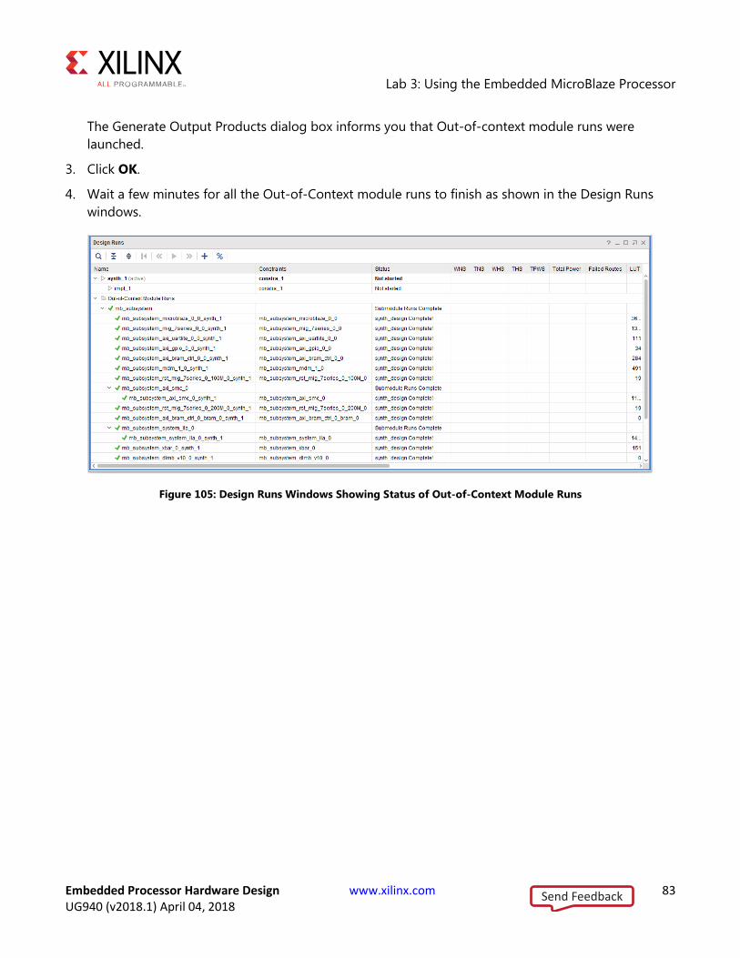
Lab 3: Using the Embedded MicroBlaze Processor
Embedded Processor Hardware Design www.xilinx.com 83 UG940 (v2018.1) April 04, 2018
The Generate Output Products dialog box informs you that Out-of-context module runs were
launched.
3. Click OK.
4. Wait a few minutes for all the Out-of-Context module runs to finish as shown in the Design Runs
windows.
Figure 105: Design Runs Windows Showing Status of Out-of-Context Module Runs
Send Feedback
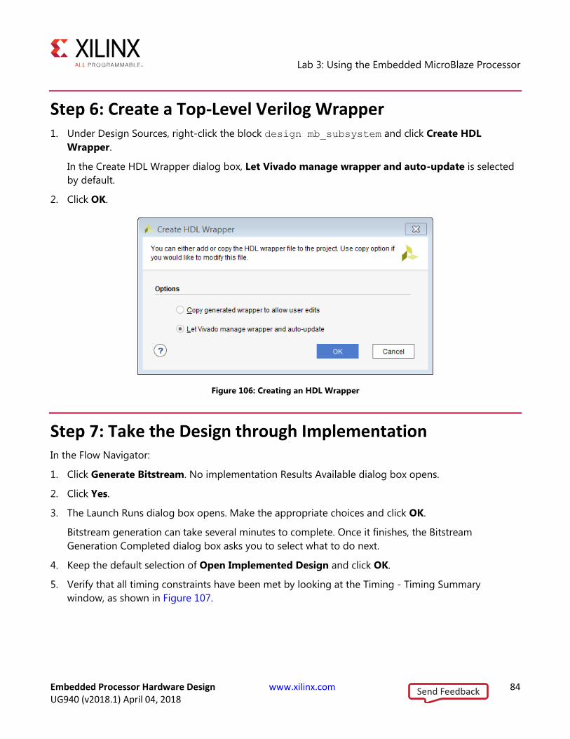
Lab 3: Using the Embedded MicroBlaze Processor
Embedded Processor Hardware Design www.xilinx.com 84 UG940 (v2018.1) April 04, 2018
Step 6: Create a Top-Level Verilog Wrapper 1. Under Design Sources, right-click the block design mb_subsystem and click Create HDL
Wrapper.
In the Create HDL Wrapper dialog box, Let Vivado manage wrapper and auto-update is selected
by default.
2. Click OK.
Figure 106: Creating an HDL Wrapper
Step 7: Take the Design through Implementation In the Flow Navigator:
1. Click Generate Bitstream. No implementation Results Available dialog box opens.
2. Click Yes.
3. The Launch Runs dialog box opens. Make the appropriate choices and click OK.
Bitstream generation can take several minutes to complete. Once it finishes, the Bitstream
Generation Completed dialog box asks you to select what to do next.
4. Keep the default selection of Open Implemented Design and click OK.
5. Verify that all timing constraints have been met by looking at the Timing - Timing Summary
window, as shown in Figure 107.
Send Feedback

Lab 3: Using the Embedded MicroBlaze Processor
Embedded Processor Hardware Design www.xilinx.com 85 UG940 (v2018.1) April 04, 2018
Figure 107: Timing Summary
Step 8: Exporting the Design to SDK Next, open the design and export to SDK.
1. Select File > Export > Export Hardware.
2. In the Export to Hardware dialog box, select the Include bitstream check box, shown in the
following figure Make sure that the Export to field is set to <Local to Project>.
Figure 108: Export to Hardware Dialog Box
3. Click OK.
4. Select File > Launch SDK. In the Launch SDK dialog box, shown in the following figure, make sure
that both the Exported location and the Workspace drop-down lists are set to
<Local to Project>.
Send Feedback
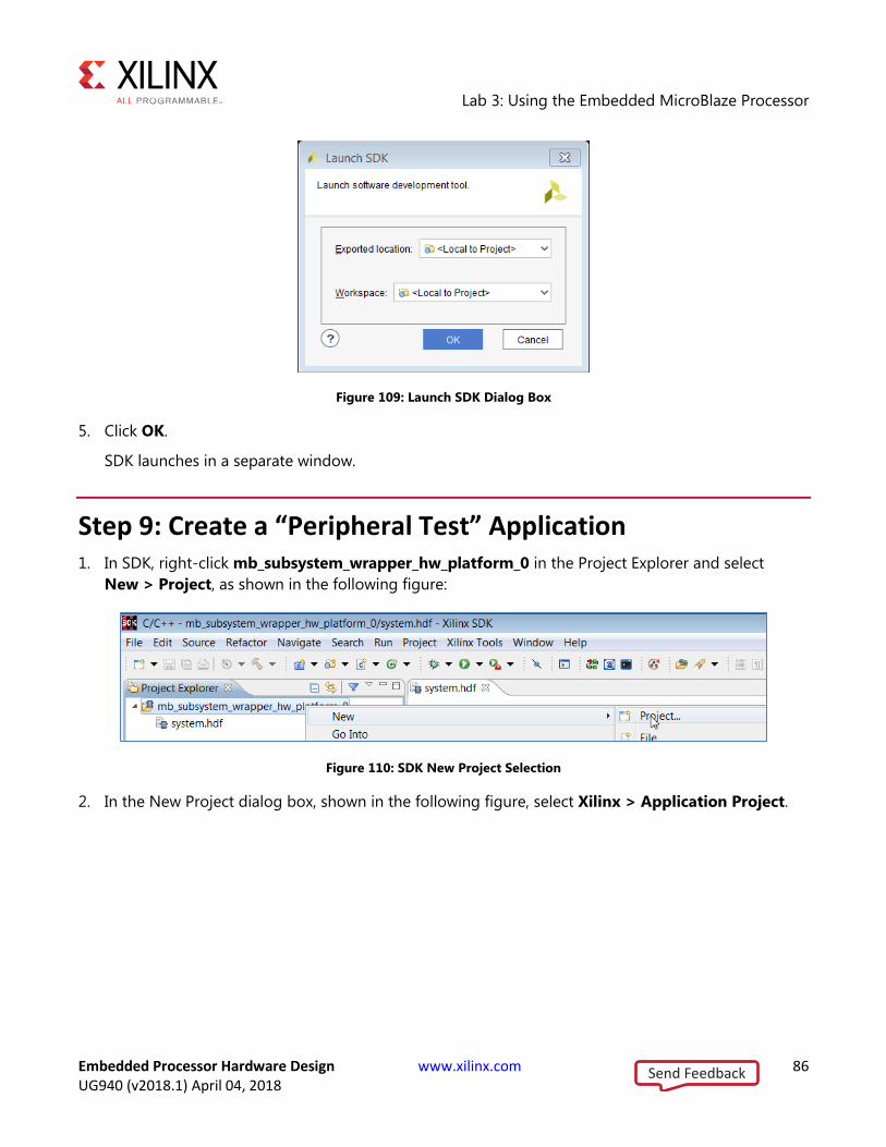
Lab 3: Using the Embedded MicroBlaze Processor
Embedded Processor Hardware Design www.xilinx.com 86 UG940 (v2018.1) April 04, 2018
Figure 109: Launch SDK Dialog Box
5. Click OK.
SDK launches in a separate window.
Step 9: Create a “Peripheral Test” Application 1. In SDK, right-click mb_subsystem_wrapper_hw_platform_0 in the Project Explorer and select
New > Project, as shown in the following figure:
Figure 110: SDK New Project Selection
2. In the New Project dialog box, shown in the following figure, select Xilinx > Application Project.
Send Feedback

Lab 3: Using the Embedded MicroBlaze Processor
Embedded Processor Hardware Design www.xilinx.com 87 UG940 (v2018.1) April 04, 2018
Figure 111: SDK New Project Wizard
3. Click Next.
4. Type a name (such as peri_test) for your project and choose standalone as the OS platform, as
displayed in Figure 112.
Send Feedback
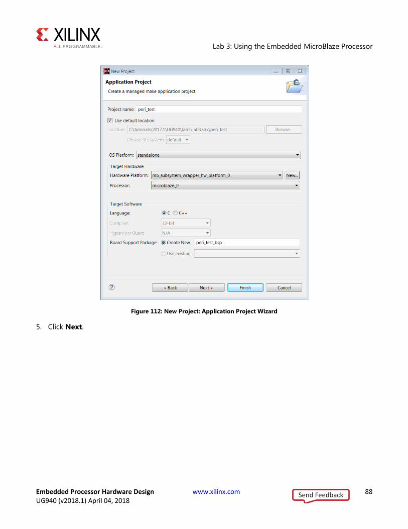
Lab 3: Using the Embedded MicroBlaze Processor
Embedded Processor Hardware Design www.xilinx.com 88 UG940 (v2018.1) April 04, 2018
Figure 112: New Project: Application Project Wizard
5. Click Next.
Send Feedback

Lab 3: Using the Embedded MicroBlaze Processor
Embedded Processor Hardware Design www.xilinx.com 89 UG940 (v2018.1) April 04, 2018
6. Select the application template, shown in the following figure, and click Finish.
Figure 113: New Project: Template Wizard
SDK creates a new “peri_test” application.
7. Wait for the application to finish compiling.
8. Right-click the peri_test application in the Project Explorer and select Generate Linker Script.
The Generate Linker Script dialog box opens, as shown in Figure 114.
Send Feedback

Lab 3: Using the Embedded MicroBlaze Processor
Embedded Processor Hardware Design www.xilinx.com 90 UG940 (v2018.1) April 04, 2018
9. Select the Basic tab and change the Assigned Memory for Heap and Stack to mig_7series_0.
Figure 114: Basic Tab of the Generate a Linker Script Dialog Box
Send Feedback
Lab 3: Using the Embedded MicroBlaze Processor
Embedded Processor Hardware Design www.xilinx.com 91 UG940 (v2018.1) April 04, 2018
10. The Advanced options all change to mig_7_series_0 as shown below.
Figure 115: Generate Linker Script Dialog Box
Setting these values to mig_7series_0 ensures that the compiled code executes from the
Memory IP.
11. Click Generate.
12. Click Yes to overwrite it in the Linker Script Already Exists! dialog box.
Send Feedback

Lab 3: Using the Embedded MicroBlaze Processor
Embedded Processor Hardware Design www.xilinx.com 92 UG940 (v2018.1) April 04, 2018
Step 10: Executing the Software Application on a KC705 Board Make sure that you have connected the target board to the host computer and it is turned on.
1. Select Xilinx Tools > Program FPGA to open the Program FPGA dialog box.In the Program FPGA
dialog box, click Program, as shown in the following figure:
Figure 116: Program FPGA Dialog Box
2. Select and right-click the peri_test application in the Project Explorer, and select
Debug As > Debug Configurations.
Send Feedback

Lab 3: Using the Embedded MicroBlaze Processor
Embedded Processor Hardware Design www.xilinx.com 93 UG940 (v2018.1) April 04, 2018
The Debug Configurations dialog box opens, as shown in the following figure.
3. Right-click Xilinx C/C++ application (System Debugger), and select New.
Figure 117: Create New Debug Configuration
4. Click Debug.
Send Feedback
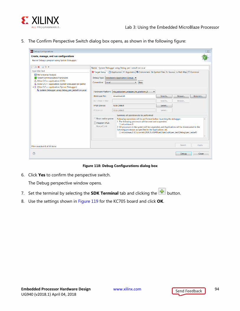
Lab 3: Using the Embedded MicroBlaze Processor
Embedded Processor Hardware Design www.xilinx.com 94 UG940 (v2018.1) April 04, 2018
5. The Confirm Perspective Switch dialog box opens, as shown in the following figure:
Figure 118: Debug Configurations dialog box
6. Click Yes to confirm the perspective switch.
The Debug perspective window opens.
7. Set the terminal by selecting the SDK Terminal tab and clicking the button.
8. Use the settings shown in Figure 119 for the KC705 board and click OK.
Send Feedback
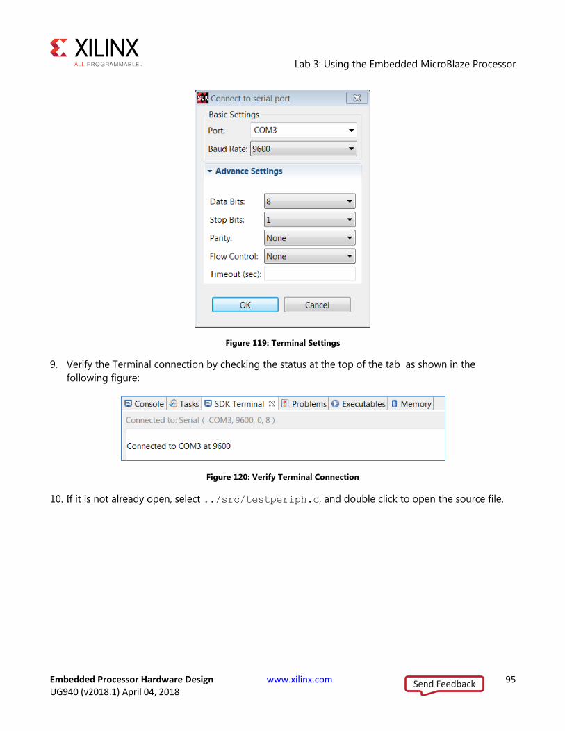
Lab 3: Using the Embedded MicroBlaze Processor
Embedded Processor Hardware Design www.xilinx.com 95 UG940 (v2018.1) April 04, 2018
Figure 119: Terminal Settings
9. Verify the Terminal connection by checking the status at the top of the tab as shown in the
following figure:
Figure 120: Verify Terminal Connection
10. If it is not already open, select ../src/testperiph.c, and double click to open the source file.
Send Feedback
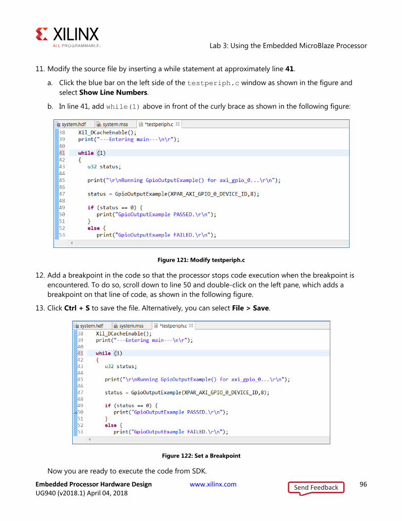
Lab 3: Using the Embedded MicroBlaze Processor
Embedded Processor Hardware Design www.xilinx.com 96 UG940 (v2018.1) April 04, 2018
11. Modify the source file by inserting a while statement at approximately line 41.
a. Click the blue bar on the left side of the testperiph.c window as shown in the figure and
select Show Line Numbers.
b. In line 41, add while(1) above in front of the curly brace as shown in the following figure:
Figure 121: Modify testperiph.c
12. Add a breakpoint in the code so that the processor stops code execution when the breakpoint is
encountered. To do so, scroll down to line 50 and double-click on the left pane, which adds a
breakpoint on that line of code, as shown in the following figure.
13. Click Ctrl + S to save the file. Alternatively, you can select File > Save.
Figure 122: Set a Breakpoint
Now you are ready to execute the code from SDK.
Send Feedback

Lab 3: Using the Embedded MicroBlaze Processor
Embedded Processor Hardware Design www.xilinx.com 97 UG940 (v2018.1) April 04, 2018
Step 11: Connect to Vivado Logic Analyzer Connect to the KC705 board using the Vivado Logic Analyzer.
1. In the Vivado IDE session, from the Program and Debug drop-down list of the Vivado Flow
Navigator, select Open Hardware Manager.
2. In the Hardware Manager window, click Open target > Open New Target.
Figure 123: Open a New Hardware Target
Note: You can also use the Auto Connect option to connect to the target hardware.
The Open New Hardware Target dialog box opens, shown in the following figure:
3. Click Next.
Figure 124: Open Hardware Target
Send Feedback

Lab 3: Using the Embedded MicroBlaze Processor
Embedded Processor Hardware Design www.xilinx.com 98 UG940 (v2018.1) April 04, 2018
On the Hardware Server Settings page, ensure that the Connect to field is set to Local server
(target is on local machine), as shown in the following figure:
4. Click Next.
Figure 125: Specify Server Name
5. On the Select Hardware Target page, shown below, click Next.
Figure 126: Select Hardware Target
Send Feedback

Lab 3: Using the Embedded MicroBlaze Processor
Embedded Processor Hardware Design www.xilinx.com 99 UG940 (v2018.1) April 04, 2018
6. Ensure that all the settings are correct on the Open Hardware Target Summary dialog box and click
Finish.
Figure 127: Open Hardware Target Summary
Step 12: Setting the MicroBlaze to Logic Cross Trigger When the Vivado Hardware Session successfully connects to the ZC702 board, you see the
information shown in the following figure:
Figure 128: Vivado Hardware Window
Send Feedback

Lab 3: Using the Embedded MicroBlaze Processor
Embedded Processor Hardware Design www.xilinx.com 100 UG940 (v2018.1) April 04, 2018
1. Select the Settings - hw_ila_1 tab and set the Trigger Mode Settings as follows:
Set Trigger mode to TRIG_IN_ONLY
Set TRIG_OUT mode to TRIG_IN_ONLY
Under Capture Mode Settings, ensure that Trigger position in window is set to 512.
Figure 129: Set ILA Properties for hw_ila_1
2. Arm the ILA core by clicking the Run Trigger button .
This arms the ILA and you should see the status “Waiting for Trigger” as shown in
Figure 130.
Send Feedback

Lab 3: Using the Embedded MicroBlaze Processor
Embedded Processor Hardware Design www.xilinx.com 101 UG940 (v2018.1) April 04, 2018
Figure 130: Armed ILA Core
3. In SDK, in the Debug window, click the MicroBlaze #0 in the Debug window and click the Resume
button . The code will execute until the breakpoint set on Line 50 in testperiph.c file is
reached. As the breakpoint is reached, this triggers the ILA, as seen in the following figure:
Figure 131: MicroBlaze to Logic Cross Trigger Waveform in hw_ila_1
This demonstrates that when the breakpoint is encountered during code execution, the MicroBlaze
triggers the ILA that is set up to trigger. This way you can monitor the state of the hardware at a certain
point of code execution.
Send Feedback

Lab 3: Using the Embedded MicroBlaze Processor
Embedded Processor Hardware Design www.xilinx.com 102 UG940 (v2018.1) April 04, 2018
Step 13: Setting the Logic to Processor Cross-Trigger Now try the logic to processor side of the cross-trigger mechanism. In other words, remove the
breakpoint that you set earlier on line 50 to have the ILA trigger the processor and stop code execution.
To do this:
1. Select the Breakpoints tab towards the top right corner of SDK window, and uncheck the
testperiph.c [line: 50] checkbox. This removes the breakpoint that you set up earlier.
Note: Alternatively, you can also click on the breakpoint in the testperiph.c file and select Disable
Breakpoint.
2. In the Debug window, right-click the MicroBlaze #0 target and select Resume. The code runs
continuously because it has an infinite loop.
You can see the code executing in the Terminal Window in SDK.
3. In Vivado, select the Settings - hw_ila_1 tab. Change the Trigger Mode to BASIC_OR_TRIG_IN and
the TRIG_OUT mode to TRIGGER_OR_TRIG_IN.
4. Click on the + sign in the Trigger Setup window to add the
slot_0:microblaze_0_axi_periph_M01:AWVALID signal from the Add Probes window.
5. In the Basic Trigger Setup window, for slot_0:microblaze_0_axi_periph_M01:AWVALID
signal, ensure that the Radix field is set to [B] (Binary) and set the Value field to 1. This essentially
sets up the ILA to trigger when the awvalid transitions to a value of 1.
6. Click the Run Trigger button to “arm” the ILA in the Status – hw_ila_1 window. The ILA immediately
triggers as the application software is continuously performing a write to the GPIO thereby toggling
the net_slot_0_axi_awvalid signal, which causes the ILA to trigger. The ILA in turn, toggles
the TRIG_OUT signal, which signals the processor to stop code execution.
This is seen in SDK the in the highlighted area of the debug window.
Figure 132: Verify that the Processor Has Been Interrupted in SDK
Send Feedback

Lab 3: Using the Embedded MicroBlaze Processor
Embedded Processor Hardware Design www.xilinx.com 103 UG940 (v2018.1) April 04, 2018
Conclusion In this tutorial, you:
Stitched together a design in the Vivado IP integrator tool
Took the design through implementation and bitstream generation
Exported the hardware to SDK
Created and modified application code that runs on a Standalone Operating System
Modified the linker script so that the code executes from the DDR3
Verified cross-trigger functionality between the MicroBlaze processor executing code and the
design logic
Lab Files The Tcl script lab3.tcl is included with the design files to perform all the tasks in Vivado. The SDK
operations must be done in the SDK GUI. You might need to modify the Tcl script to match the project
path and project name on your machine.
Send Feedback

Embedded Processor Hardware Design www.xilinx.com 104 UG940 (v2018.1) April 04, 2018
Legal Notices
Please Read: Important Legal Notices The information disclosed to you hereunder (the “Materials”) is provided solely for the selection and use of Xilinx products. To the maximum
extent permitted by applicable law: (1) Materials are made available "AS IS" and with all faults, Xilinx hereby DISCLAIMS ALL WARRANTIES
AND CONDITIONS, EXPRESS, IMPLIED, OR STATUTORY, INCLUDING BUT NOT LIMITED TO WARRANTIES OF MERCHANTABILITY,
NON-INFRINGEMENT, OR FITNESS FOR ANY PARTICULAR PURPOSE; and (2) Xilinx shall not be liable (whether in contract or tort,
including negligence, or under any other theory of liability) for any loss or damage of any kind or nature related to, arising under, or in
connection with, the Materials (including your use of the Materials), including for any direct, indirect, special, incidental, or consequential loss
or damage (including loss of data, profits, goodwill, or any type of loss or damage suffered as a result of any action brought by a third party)
even if such damage or loss was reasonably foreseeable or Xilinx had been advised of the possibility of the same. Xilinx assumes no
obligation to correct any errors contained in the Materials or to notify you of updates to the Materials or to product specifications. You may not
reproduce, modify, distribute, or publicly display the Materials without prior written consent. Certain products are subject to the terms and
conditions of Xilinx’s limited warranty, please refer to Xilinx’s Terms of Sale which can be viewed at https://www.xilinx.com/legal.htm#tos; IP
cores may be subject to warranty and support terms contained in a license issued to you by Xilinx. Xilinx products are not designed or
intended to be fail-safe or for use in any application requiring fail-safe performance; you assume sole risk and liability for use of Xilinx products
in such critical applications, please refer to Xilinx’s Terms of Sale which can be viewed at https://www.xilinx.com/legal.htm#tos.
AUTOMOTIVE APPLICATIONS DISCLAIMER
AUTOMOTIVE PRODUCTS (IDENTIFIED AS “XA” IN THE PART NUMBER) ARE NOT WARRANTED FOR USE IN THE DEPLOYMENT OF
AIRBAGS OR FOR USE IN APPLICATIONS THAT AFFECT CONTROL OF A VEHICLE (“SAFETY APPLICATION”) UNLESS THERE IS A
SAFETY CONCEPT OR REDUNDANCY FEATURE CONSISTENT WITH THE ISO 26262 AUTOMOTIVE SAFETY STANDARD (“SAFETY
DESIGN”). CUSTOMER SHALL, PRIOR TO USING OR DISTRIBUTING ANY SYSTEMS THAT INCORPORATE PRODUCTS,
THOROUGHLY TEST SUCH SYSTEMS FOR SAFETY PURPOSES. USE OF PRODUCTS IN A SAFETY APPLICATION WITHOUT A
SAFETY DESIGN IS FULLY AT THE RISK OF CUSTOMER, SUBJECT ONLY TO APPLICABLE LAWS AND REGULATIONS GOVERNING
LIMITATIONS ON PRODUCT LIABILITY.
© Copyright 2013 – 2018 Xilinx, Inc. Xilinx, the Xilinx logo, Artix, ISE, Kintex, Spartan, Virtex, Zynq, and other designated brands included
herein are trademarks of Xilinx in the United States and other countries. All other trademarks are the property of their respective owners.
Send Feedback


