
International Journal of Scientific Research and Engineering Studies (IJSRES)
Volume 3 Issue 7, July 2016
ISSN: 2349-8862
www.ijsres.com Page 21
Various Modeling Methods For The Analysis Of A Three Phase
Diode Bridge Rectifier And A Three Phase Inverter
Parvathi M. S
PG Scholar, Dept of EEE, Mar Baselios College of
Engineering and Technology, Trivandrum
Dr. Nisha G. K
Associate Professor, Dept of EEE, Mar Baselios College of
Engineering and Technology, Trivandrum
Abstract: This paper presents the modelling of a three
phase diode rectifier and a three phase inverter in the
Modified Nodal Analysis method and in the Average method.
Virtually all electronic devices require DC, so rectifiers are
used inside the power supplies of all electronic equipment.
Inverters are extensively used in power electronic
applications for converting DC to AC. The applications of
inverters range from uninterrupted power supplies used in
home appliances control to HVDC power transmission. The
average model equations for rectifier and inverter are
formulated using the Forward Euler method.
Keywords: Average Method, Modified Nodal Analysis
method, Three phase diode bridge rectifier and Three phase
inverter.
I. INTRODUCTION
As technology grows every day, the study of power
systems has shifted its direction to power electronics to
produce the most efficient energy conversion. Power
electronics is the study of processing and controlling the flow
of electric energy by supplying voltages and currents in a form
that is suited for user loads [1]. The goals of using power
electronics are to obtain the benefit of lower cost, small power
loss and high energy efficiency. Because of high energy
efficiency, the removal of heat generated due to dissipated
energy is lower.
A rectifier is a “power processor that should give a dc
output voltage with a minimum amount of harmonic contents”
[2]. When a polyphase ac is rectified, the phase-shifted pulses
overlap each other which produce a smoother dc output than
that made by a single-phase ac rectifier. In [3], the author
presents the modeling of single phase, three phase rectifiers
and suitable controller design for the modeled rectifier circuit.
An average inverter model operating in two
complementary modes suitable for micro grid simulation
applications is proposed in [4], by taking into account the
nonlinear behaviour of the switches, delays in the control
loops, and the practical constraints. In [5], the author focuses
on a combination of three-phase Voltage Source Inverter
(VSI) with a predictive current control to provide an optimized
system for three-phase inverter that controls the load current.
With the advent of increased use of inverters, various
switching models are established. The average method is
shown to be an effective method for analysis and controller
design in inverters [6] – [8]. Conventional switching models
and state-space averaging methods which take dead-time
effects into consideration have been applied successfully in
the inverters [9], [10].
II. MODELING OF THREE PHASE DIODE BRIDGE
RECTIFIER
The modeling of a three phase diode bridge rectifier can
be done in two ways – the Modified Nodal Analysis method
and the average model method (using transient simulation
techniques). On comparing the two methods, the Modified
Nodal Analysis method is a bit too long process where, we
need to find the nodal equations and the inverse matrix at each
switching conditions. On the other hand the latter provides
transient equations which enables to obtain the output dc
voltage and current, without the calculation of matrices. The
main advantage of the average model method of modeling of
diode bridge rectifier is that it provides ripple free output.
A. MODIFIED NODAL ANALYSIS METHOD
The power circuit diagram for a three phase diode bridge
rectifier is as shown in the Fig. 1.

International Journal of Scientific Research and Engineering Studies (IJSRES)
Volume 3 Issue 7, July 2016
ISSN: 2349-8862
www.ijsres.com Page 22
Figure 1: Circuit Diagram of a three phase diode bridge
rectifier
Figure 2: Input Output waveforms and the diode conduction
period of a three phase diode rectifier
The diodes are arranged in three legs. Each leg has two
series-connected diodes. The upper diodes D1, D3, D5
constitute the positive group of diodes. The lower diodes D2,
D4, D6 form the negative group of diodes. The diodes D1, D3,
D5 forming the positive group, would conduct when these
experience the highest positive voltage. Likewise, the diodes
D2, D4, D6 would conduct when these are subjected to most
negative voltage. For a particular interval, a diode from the
positive group and a diode from the negative group conduct.
No two diodes from the same group conduct together at a
time. The waveforms for the three phase diode rectifier and
each diode‟s corresponding conducting period are as shown in
the Fig. 2.
It is seen from the source voltage waveform that, from ωt
= 30 to 150°, voltage Va is more positive than the voltages Vb
and Vc. Therefore, the diode D1 connected to line „a‟ conducts
during this interval [11]. Likewise, from ωt = 150 to 270°,
voltage Vb is more positive therefore, diode D3 conducts.
Similarly, diode D5 from the positive group conducts from ωt
= 270 to 390° and so on. Conduction of the positive group
diodes is shown in Fig. 2 as D5, D1, D3, D5 etc. Similarly, the
negative diodes also conduct accordingly.
A three phase diode bridge rectifier consists of six diodes
arranged in three legs. Each diode has an on-resistance value
Ron, when the diode conducts and an off-resistance value Roff,
when the diode is not conducting. For the analysis purpose,
the three phase diode bridge rectifier is replaced by its
equivalent circuit diagram with its on-state and off-state
resistance values. The equivalent circuit diagram is obtained
for each conduction period, where two diodes conduct, one
diode from the positive group and the other from the negative
group.
Consider the interval ωt = 0 to 30° and ωt = 330 to
360°, where the diodes D5 and D6 conduct. The conducting
diodes D5 and D6 are replaced by their on-resistance values
Ron and the rest of the diodes with their off-resistance values
Roff. The equivalent circuit diagram will be as in Fig. 3.
Figure 3: Equivalent circuit diagram of a three phase diode
bridge rectifier for the interval ωt = 0 to 30° and ωt = 330
to 360° (D5 and D6 conduct)
Now, applying KCL at the nodes a, b, c and d, we get the
following equations.
At node „a‟;
At node „b‟;
At node „c‟;
At node „d‟;
Converting the above nodal equations into matrix form
which amounts to solve a linear system AX = Z, where, A
denotes the admittance matrix or the modified nodal analysis
matrix, X denotes the unknown matrix (unknown node
voltages and currents) and Z is the input matrix (source
voltages). We can obtain the unknown matrix X as X = A-1
Z.

International Journal of Scientific Research and Engineering Studies (IJSRES)
Volume 3 Issue 7, July 2016
ISSN: 2349-8862
www.ijsres.com Page 23
Assuming suitable values for the resistances as Ron =
1mΩ, Roff = 1MΩ, RL = 10kΩ and substituting in the above
matrix equation, the inverse of A matrix (A-1
) can be obtained
using an online inverse matrix calculator. The A-1
matrix (after
substituting the resistance values) for the interval taken, ωt =
0 to 30° and ωt = 330 to 360°, can be evaluated as below.
During the interval, ωt = 30 to 90°, the diodes D1 and D6
will be conducting and the inverse matrix can be obtained as
below.
Similarly, A
-1 matrix for each conducting interval can be
obtained. The A-1
matrix and the Z matrix is given as input to
the program and the corresponding outputs waveforms are
obtained.
B. AVERAGE METHOD FOR RECTIFIER MODELING
USING TRANSIENT SIMULATION TECHNIQUES
In order to make prime decisions in the design
procedures, power electronic modeling methods are widely
used. The modeled circuit helps to determine the performance
of the circuit along with the component values as well. State
space average modeling method is a common technique that is
utilized to obtain models of power electronic circuits for ac
and dc power conversions. The main advantage of this
particular method is that the accuracy can be increased and
ripple free waveforms can be obtained.
A simplified three phase diode bridge rectifier is shown in
the Fig. 4. The circuit consists of three ac input sources (VA,
VB and VC), input source reactor (Ls), diodes (D1 to D6),
output inductance (Lout), output filter capacitance (C) and
resistance (R) which represents the load on the rectifier [12].
Figure 4: Simplified circuit model of a three phase diode
bridge rectifier
Utilizing the general state space averaging method, the
switching functions sa, sb and sc for a three phase diode bridge
rectifier can be expressed by a Fourier series using the first
harmonic terms of the series as shown in the equation (5).
The average dc output voltage Vpn can be expressed as the
equation (6).
Also, the dc current equation can be obtained as shown in
equation (7).
From the equation (6), the left hand side of the equation
can be expanded as:
Now, the right hand side of the equation (6) can be solved
using the Transient simulation method. In this method, the
differential current equation can be converted to its equivalent
Forward Euler form and solved to obtain the value for the
(n+1)th
value of the dc current.
From the equation (9), the (n+1)
th value of the dc current
can be calculated as:
where, „h‟ is the delta constant value or the time step.
Similarly, from the equation (7), the differential voltage
equation can be converted to its equivalent Forward Euler
form and solved to obtain the value for the (n+1)th
value of the
dc voltage.
Thus, from the equation (11), the (n+1)
th value of the dc
voltage can be calculated as:
The modeling equation for a three phase diode bridge
rectifier is obtained using the average state space model and

International Journal of Scientific Research and Engineering Studies (IJSRES)
Volume 3 Issue 7, July 2016
ISSN: 2349-8862
www.ijsres.com Page 24
the transient simulation techniques. The equations (8), (10)
and (12) represent the average model mathematical equations
for the rectifier output dc voltage and dc current.
III. MODELING OF THREE PHASE INVERTER
Similar to the modeling of a three phase diode bridge
rectifier, a three phase inverter can also be done in two ways –
the Modified Nodal Analysis method and the average model
method (using transient simulation techniques). The main
advantage of the ripple free output in the case of the average
model method holds the same for the modeling of a three
phase inverter as well.
A. MODIFIED NODAL ANALYSIS METHOD
A basic three phase inverter is a six-step bridge inverter.
It uses a minimum of six thyristors. In inverter terminology, a
step is defined as a change in the firing from one thyristor to
the next thyristor in the proper sequence. For one cycle of
360°, each step would be of 60° interval for a six-step inverter.
This means that the thyristors would be gated at regular
intervals of 60° in proper sequence so that a three phase ac
voltage is synthesized at the output terminals of a six-step
inverter.
The Fig. 5 shows the power circuit diagram of a three
phase bridge inverter using six thyristors and six diodes.
Presently, the use of IGBTs in single phase and three phase
inverters is on the rise. The basic circuit configuration of
inverter, however, remains unaltered with just a small change
of replacing the thyristors with IGBTs. A large capacitor
connected at the input terminals tends to make the input dc
voltage constant. This capacitor also suppresses the harmonics
fed back to the dc source. In the Fig. 5, commutation and
snubber circuits are omitted for simplicity. The thyristors are
numbered in the sequence in which they are triggered to
obtain voltages vab, vbc, vca at the output terminals a, b, c of the
inverter. There are two possible patterns of gating the
thyristors. In one pattern, each thyristor conducts for 180° and
in the other, each thyristor conducts for 120°. But in both
these patterns, gating signals are applied and removed at 60°
intervals of the output voltage waveform.
Figure 5: Circuit Diagram of a three phase bridge inverter
using thyristors
In three phase inverter, each thyristor conducts for 180° of
a cycle. The thyristor pair in each arm, i.e. T1, T4; T3, T6 and
T5, T2 are turned on with a time interval of 180. The thyristors
in the upper group, i.e. T1, T3, T5 conduct at an interval of
120°. The conduction time periods for 180° mode 3 phase
inverter is as shown in the Fig. 6. It can be understood from
the table that in every step of 60° duration, only three
thyristors are conducting – one from the upper group and two
from the lower group or vice versa.
Figure 6: Conduction period for a 180° mode 3-phase VSI
Similar to the analysis of a three phase diode bridge
rectifier, a three phase bridge inverter consists of six thyristors
arranged in three legs. Each thyristor has an on-resistance
value Ron, when the thyristor conducts and an off-resistance
value Roff, when it is not conducting. For the analysis purpose,
the three phase bridge inverter is replaced by its equivalent
circuit diagram with its on-state and off-state resistance
values. The equivalent circuit diagram is obtained for each
conduction period, where three thyristors conduct, one
thyristor from the upper group and two from the lower group
or vice versa.
Consider the interval ωt = 0 to 60°, where the thyristors
T1, T5 and T6 conduct. The conducting thyristors are replaced
by their on-resistance values Ron and the rest of the thyristors
with their off-resistance values Roff. The equivalent circuit
diagram will be as in Fig. 7.
Figure 7: Equivalent circuit diagram of a three phase bridge
inverter for the interval ωt = 0 to 60° (T1, T5 and T6 conduct)
Now, applying KCL at the nodes a, b, c and d, we get the
following equations.
At node „a‟;
At node „b‟;
At node „c‟;
International Journal of Scientific Research and Engineering Studies (IJSRES)
Volume 3 Issue 7, July 2016
ISSN: 2349-8862
www.ijsres.com Page 25
At node „d‟;
At node „o‟
Converting the above nodal equations into matrix form
which amounts to solve a linear system AX = Z, where, A
denotes the admittance matrix or the modified nodal analysis
matrix, X denotes the unknown matrix (unknown node
voltages and currents) and Z is the input matrix (source
voltages). We can obtain the unknown matrix X as X = A-1
Z.
Assuming suitable values for the resistances as Ron =
1mΩ, Roff = 1MΩ, RL = 10kΩ and substituting in the above
matrix equation, the inverse of A matrix (A-1
) can be obtained
using an online inverse matrix calculator. The A-1
matrix (after
substituting the resistance values) for the interval taken, ωt =
0 to 60° can be evaluated as below.
During the interval, ωt = 60 to 120°, the diodes T1, T2and
T6 will be conducting and the inverse matrix can be obtained
as below.
Similarly, A
-1 matrix for each conducting interval can be
obtained. The A-1
matrix and the Z matrix is given as input to
the program and the corresponding outputs waveforms are
obtained.
B. AVERAGE METHOD FOR 3 PHASE INVERTER
MODELING USING TRANSIENT SIMULATION
TECHNIQUES
In the study of inverters and their dynamic performance,
various switching models are obtained based on the switching
conditions, as in the Modified Nodal Analysis method, which
is feasible for a single inverter or a small scale inverter
system. Therefore, in case of large scale inverter systems,
switching models becomes complicated. Hence, a state space
averaging method is formulated which is effective for the
analysis and controller design purpose in inverters.
A generalized state space averaging model is considered
which enhances the fundamental AC voltage and current
calculation with desired accuracy and precision. At the same
time, this method enables the steady state as well as transient
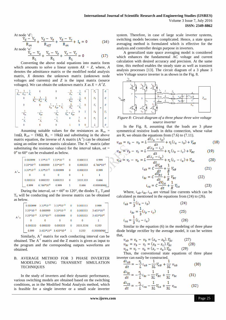
analysis processes [13]. The circuit diagram of a 3 phase 3
wire Voltage source inverter is as shown in the Fig. 8.
Figure 8: Circuit diagram of a three phase three wire voltage
source inverter
In the Fig. 8, assuming that the loads are 3 phase
symmetrical resistive loads in delta connection, whose value
are R, we obtain the equations from (7.6) to (7.11).
Where, are virtual line currents which can be
calculated as mentioned in the equations from (24) to (26).
Similar to the equation (6) in the modeling of three phase
diode bridge rectifier by the average model, it can be written
that,
Thus, the conventional state equations of three phase
inverter can easily be constructed.
International Journal of Scientific Research and Engineering Studies (IJSRES)
Volume 3 Issue 7, July 2016
ISSN: 2349-8862
www.ijsres.com Page 26
The differential voltage and current equations can be
converted to its equivalent Forward Euler form and
substituting the equations (27) to (29) in the Forward Euler
equations we obtain the value for the (n+1)th
value of the
corresponding ac voltage and ac current.
The switching function is given by:
where k = a, b, c ; m is the modulation ratio taken as 0.5
; where is the
initial phase angle.
Thus, the modelling equations are formed for a three
phase inverter in average model using the Transient simulation
techniques.
IV. RESULTS AND DISCUSSIONS
The output waveforms obtained by simulating the MNA
model of rectifier with the parameter specification as Ron=1
mΩ, Roff=1 MΩ and RL=10 kΩ is as shown in the Fig. 9. It
depicts rectifier output voltage with amplitude 100 V.
Figure 9: Rectifier output voltage waveform in MNA method
(X axis: 1 unit = 0.002s & Yaxis: 1 unit = 10V)
In the case of the average model of the three phase diode
bridge rectifier, the parameter specifications used for the
simulation are as in the Table 1.
SYMBOL PARAMETERS VALUE UNIT
Vabc Input Voltage 415 V
f Fundamental
frequency
50 Hz
L Filtering Inductor 0.05 H
C Filter Capacitor 0.05 F
R Load Resistance 2 Ω
h Time step 100 µs
Table 1: Parameters for rectifier simulation in average model
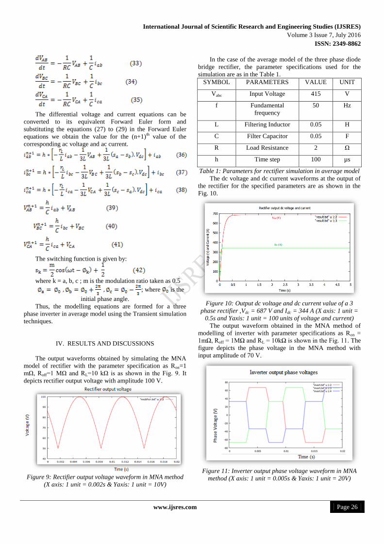
The dc voltage and dc current waveforms at the output of
the rectifier for the specified parameters are as shown in the
Fig. 10.
Figure 10: Output dc voltage and dc current value of a 3
phase rectifier ,Vdc = 687 V and Idc = 344 A (X axis: 1 unit =
0.5s and Yaxis: 1 unit = 100 units of voltage and current)
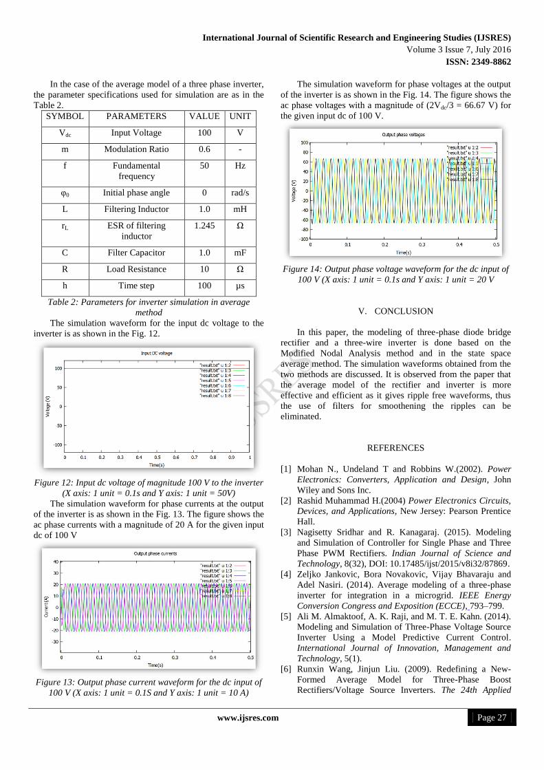
The output waveform obtained in the MNA method of
modelling of inverter with parameter specifications as Ron =
1mΩ, Roff = 1MΩ and RL = 10kΩ is shown in the Fig. 11. The
figure depicts the phase voltage in the MNA method with
input amplitude of 70 V.
Figure 11: Inverter output phase voltage waveform in MNA
method (X axis: 1 unit = 0.005s & Yaxis: 1 unit = 20V)
International Journal of Scientific Research and Engineering Studies (IJSRES)
Volume 3 Issue 7, July 2016
ISSN: 2349-8862
www.ijsres.com Page 27
In the case of the average model of a three phase inverter,
the parameter specifications used for simulation are as in the
Table 2.
SYMBOL PARAMETERS VALUE UNIT
Vdc Input Voltage 100 V
m Modulation Ratio 0.6 -
f Fundamental
frequency
50 Hz
φ0 Initial phase angle 0 rad/s
L Filtering Inductor 1.0 mH
rL ESR of filtering
inductor
1.245 Ω
C Filter Capacitor 1.0 mF
R Load Resistance 10 Ω
h Time step 100 µs
Table 2: Parameters for inverter simulation in average
method
The simulation waveform for the input dc voltage to the
inverter is as shown in the Fig. 12.
Figure 12: Input dc voltage of magnitude 100 V to the inverter
(X axis: 1 unit = 0.1s and Y axis: 1 unit = 50V)
The simulation waveform for phase currents at the output
of the inverter is as shown in the Fig. 13. The figure shows the
ac phase currents with a magnitude of 20 A for the given input
dc of 100 V
Figure 13: Output phase current waveform for the dc input of
100 V (X axis: 1 unit = 0.1S and Y axis: 1 unit = 10 A)
The simulation waveform for phase voltages at the output
of the inverter is as shown in the Fig. 14. The figure shows the
ac phase voltages with a magnitude of (2Vdc/3 = 66.67 V) for
the given input dc of 100 V.
Figure 14: Output phase voltage waveform for the dc input of
100 V (X axis: 1 unit = 0.1s and Y axis: 1 unit = 20 V
V. CONCLUSION
In this paper, the modeling of three-phase diode bridge
rectifier and a three-wire inverter is done based on the
Modified Nodal Analysis method and in the state space
average method. The simulation waveforms obtained from the
two methods are discussed. It is observed from the paper that
the average model of the rectifier and inverter is more
effective and efficient as it gives ripple free waveforms, thus
the use of filters for smoothening the ripples can be
eliminated.
REFERENCES
[1] Mohan N., Undeland T and Robbins W.(2002). Power
Electronics: Converters, Application and Design, John
Wiley and Sons Inc.
[2] Rashid Muhammad H.(2004) Power Electronics Circuits,
Devices, and Applications, New Jersey: Pearson Prentice
Hall.
[3] Nagisetty Sridhar and R. Kanagaraj. (2015). Modeling
and Simulation of Controller for Single Phase and Three
Phase PWM Rectifiers. Indian Journal of Science and
Technology, 8(32), DOI: 10.17485/ijst/2015/v8i32/87869.
[4] Zeljko Jankovic, Bora Novakovic, Vijay Bhavaraju and
Adel Nasiri. (2014). Average modeling of a three-phase
inverter for integration in a microgrid. IEEE Energy
Conversion Congress and Exposition (ECCE), 793–799.
[5] Ali M. Almaktoof, A. K. Raji, and M. T. E. Kahn. (2014).
Modeling and Simulation of Three-Phase Voltage Source
Inverter Using a Model Predictive Current Control.
International Journal of Innovation, Management and
Technology, 5(1).
[6] Runxin Wang, Jinjun Liu. (2009). Redefining a New-
Formed Average Model for Three-Phase Boost
Rectifiers/Voltage Source Inverters. The 24th Applied

International Journal of Scientific Research and Engineering Studies (IJSRES)
Volume 3 Issue 7, July 2016
ISSN: 2349-8862
www.ijsres.com Page 28
Power Electronics Conference and Exposition, 1680-
1686.
[7] M. Davari, A. R. Pourshoghi, I. Salabeigi, G. B.
Gharehpetian and S. H. Fathi. (2009). A New Nonlinear
Controller Design Using Average State Space Model of
the Inverter-Based Distributed Generation to Mitigate
Power Quality Problems. International Conference on
Electronic Machines and Systems, 1-5.
[8] N. Kroutikova, C.A.Hernandez-Aramburo and T.C.
Green. (2007). State-space model of grid-connected
inverters under current control mode. The Institution of
Engineering and Technology, 1(3), 329- 338.
[9] Toni Itkonen, Julius Luukko. (2008). Switching-Function-
Based Simulation Model for Three-Phase Voltage Source
Inverter Taking Dead-Time Effects into Account. The
34th IEEE Annual Conference on Industrial Electronics,
992-997.
[10] S. Ahmed, Z. Shen, P. Mattavelli, D. Boroyevich, M.
Jaksic, K. Kamiar and J. Fu. (2011). Small-Signal Model
of a Voltage Source Inverter (VSI) Considering the Dead-
Time Effect and Space Vector Modulation Types. The
26th Applied Power Electronics Conference and
Exposition, 685-690.
[11] Dr. P. S.Bimbhra. (2009). Power Electronics: Khanna
Publishers.
[12] Joseph Maurio, Thomas Roettger, Matthew Superczynski,
(2015). Average model of a three phase controlled
rectifier valid for continuous and discontinuous
conduction modes. Transportation Electrification
Conference and Expo (ITEC), 1-7.
[13] Zhao Lin and Hao Ma. (2013). Modeling and Analysis of
Three-phase Inverter based on Generalized State Space
Averaging Method. IEEE Annual Conference on
Industrial Electronic Society. 1007-1012.


