
AT91 ARM Thumb-based Microcontrollers
AT91M55800A
Rev. 1745F–ATARM–06-Sep-07
Features• Utilizes the ARM7TDMI® ARM® Thumb® Processor Core
– High-performance 32-bit RISC Architecture– High-density 16-bit Instruction Set– Leader in MIPS/Watt– EmbeddedICE™ (In-Circuit Emulation)
• 8K Bytes Internal SRAM• Fully-programmable External Bus Interface (EBI)
– Maximum External Address Space of 128M Bytes– Eight Chip Selects– Software Programmable 8/16-bit External Databus
• 8-level Priority, Individually Maskable, Vectored Interrupt Controller– Seven External Interrupts, Including a High-priority, Low-latency Interrupt Request
• Fifty-eight Programmable I/O Lines• 6-channel 16-bit Timer/Counter
– Six External Clock Inputs and Two Multi-purpose I/O Pins per Channel• Three USARTs• Master/Slave SPI Interface
– 8-bit to 16-bit Programmable Data Length– Four External Slave Chip Selects
• Programmable Watchdog Timer• 8-channel 10-bit ADC• 2-channel 10-bit DAC• Clock Generator with On-chip Main Oscillator and PLL for Multiplication
– 3 to 20 MHz Frequency Range Main Oscillator• Real-time Clock with On-chip 32 kHz Oscillator
– Battery Backup Operation and External Alarm• 8-channel Peripheral Data Controller for USARTs and SPIs• Advanced Power Management Controller (APMC)
– Normal, Wait, Slow, Standby and Power-down modes• IEEE® 1149.1 JTAG Boundary-scan on all Digital Pins• Fully Static Operation: 0 Hz to 33 MHz• 2.7V to 3.6V Core Operating Range• 2.7V to 5.5V I/O Operating Range• 2.7V to 3.6V Analog Operating Range• 1.8V to 3.6V Backup Battery Operating Range• 2.7V to 3.6V Oscillator and PLL Operating Range• -40°C to +85°C Temperature Range• Available in a 176-lead LQFP (Green) and a 176-ball BGAPackage (RoHS-compliant)
1. DescriptionThe AT91M55800A is a member of the Atmel AT91 16/32-bit microcontroller family,which is based on the ARM7TDMI processor core. This processor has a high-perfor-mance 32-bit RISC architecture with a high-density 16-bit instruction set and very lowpower consumption. In addition, a large number of internally banked registers result invery fast exception handling, making the device ideal for real-time controlapplications.

The fully programmable External Bus Interface provides a direct connection to off-chip memory in as fast as one clockcycle for a read or write operation. An eight-level priority vectored interrupt controller in conjunction with the peripheral datacontroller significantly improve the real-time performance of the device.
The device is manufactured using Atmel’s high-density CMOS technology. By combining the ARM7TDMI processor corewith an on-chip SRAM, a wide range of peripheral functions, analog interfaces and low-power oscillators on a monolithicchip, the Atmel AT91M55800A is a powerful microcontroller that provides a highly-flexible and cost-effective solution tomany ultra low-power applications.
21745F–ATARM–06-Sep-07
AT91M5880A

AT91M5880A
2. Pin Configurations
Notes: 1. Analog pins
2. Battery backup pins
Table 2-1. Pin Configuration for 176-lead LQFP PackagePin AT91M55800A Pin AT91M55800A Pin AT91M55800A Pin AT91M55800A
1 GND 45 GND 89 GND 133 GND
2 GND 46 GND 90 GND 134 GND
3 NCS0 47 D8 91 PA19/RXD1 135 NCS4
4 NCS1 48 D9 92 PA20/SCK2 136 NCS5
5 NCS2 49 D10 93 PA21/TXD2 137 NCS6
6 NCS3 50 D11 94 PA22/RXD2 138 NCS7
7 NLB/A0 51 D12 95 PA23/SPCK 139 PB0
8 A1 52 D13 96 PA24/MISO 140 PB1
9 A2 53 D14 97 PA25/MOSI 141 PB2
10 A3 54 D15 98 PA26/NPCS0/NSS 142 PB3/IRQ4
11 A4 55 PB19/TCLK0 99 PA27/NPCS1 143 PB4/IRQ5
12 A5 56 PB20/TIOA0 100 PA28/NPCS2 144 PB5
13 A6 57 PB21/TIOB0 101 PA29/NPCS3 145 PB6/AD0TRIG
14 A7 58 PB22/TCLK1 102 VDDIO 146 PB7/AD1TRIG
15 VDDIO 59 VDDIO 103 GND 147 VDDIO
16 GND 60 GND 104 VDDPLL 148 GND
17 A8 61 PB23/TIOA1 105 XIN 149 PB8
18 A9 62 PB24/TIOB1 106 XOUT 150 PB9
19 A10 63 PB25/TCLK2 107 GNDPLL 151 PB10
20 A11 64 PB26/TIOA2 108 PLLRC 152 PB11
21 A12 65 PB27/TIOB2 109 VDDBU(2) 153 PB12
22 A13 66 PA0/TCLK3 110 XIN32(2) 154 PB13
23 A14 67 PA1/TIOA3 111 XOUT32(2) 155 PB14
24 A15 68 PA2/TIOB3 112 NRSTBU(2) 156 PB15
25 A16 69 PA3/TCLK4 113 GNDBU(2) 157 PB16
26 A17 70 PA4/TIOA4 114 WAKEUP(2) 158 PB17
27 A18 71 PA5/TIOB4 115 SHDN(2) 159 NWDOVF
28 A19 72 PA6/TCLK5 116 GNDBU(2) 160 MCKO
29 VDDIO 73 VDDIO 117 VDDA(1) 161 VDDIO
30 GND 74 GND 118 AD0(1) 162 GND
31 A20 75 PA7/TIOA5 119 AD1(1) 163 PB18/BMS
32 A21 76 PA8/TIOB5 120 AD2(1) 164 JTAGSEL
33 A22 77 PA9/IRQ0 121 AD3(1) 165 TMS
34 A23 78 PA10/IRQ1 122 AD4(1) 166 TDI
35 D0 79 PA11/IRQ2 123 AD5(1) 167 TDO
36 D1 80 PA12/IRQ3 124 AD6(1) 168 TCK
37 D2 81 PA13/FIQ 125 AD7(1) 169 NTRST
38 D3 82 PA14/SCK0 126 ADVREF(1) 170 NRST
39 D4 83 PA15/TXD0 127 DAVREF(1) 171 NWAIT
40 D5 84 PA16/RXD0 128 DA0(1) 172 NOE/NRD
41 D6 85 PA17/SCK1 129 DA1(1) 173 NWE/NWR0
42 D7 86 PA18/TXD1/NTRI 130 GNDA(1) 174 NUB/NWR1
43 VDDCORE 87 VDDCORE 131 VDDCORE 175 VDDCORE
44 VDDIO 88 VDDIO 132 VDDIO 176 VDDIO
31745F–ATARM–06-Sep-07

Table 2-2. Pin Configuration for 176-ball BGA Package
Pin AT91M55800A Pin AT91M55800A Pin AT91M55800A Pin AT91M55800A
A1 NCS1 C1 A0/NLB E1 A4 G1 A12
A2 NWAIT C2 NCS0 E2 A3 G2 A9
A3 NRST C3 VDDIO E3 A5 G3 A8
A4 NTRST C4 VDDCORE E4 GND G4 GND
A5 PB18/BMS C5 TMS E5 – G5 –
A6 NWDOVF C6 VDDIO E6 – G6 –
A7 PB16 C7 MCK0 E7 – G7 –
A8 PB12 C8 PB13 E8 – G8 –
A9 PB10 C9 PB6/AD0TRIG E9 – G9 –
A10 PB9 C10 VDDIO E10 – G10 –
A11 PB8 C11 PB4/IRQ5 E11 – G11 –
A12 NCS7 C12 PB0 E12 AD6 G12 AD3
A13 NCS6 C13 VDDIO E13 AD5 G13 AD2
A14 GND C14 DA0 E14 NRSTBU G14 GND
A15 DAVREF C15 ADVREF E15 GNDBU G15 XIN32
B1 NCS2 D1 A2 F1 A10 H1 A15
B2 NUB/NWR1 D2 A1 F2 A7 H2 A14
B3 NWE/NWR0 D3 NCS3 F3 VDDIO H3 A13
B4 NOE/NRD D4 GND F4 A6 H4 A11
B5 TD0 D5 TCK F5 – H5 –
B6 TDI D6 JTAGSEL F6 – H6 –
B7 PB17 D7 GND F7 – H7 –
B8 PB11 D8 PB15 F8 – H8 –
B9 PB7/AD1TRIG D9 PB14 F9 – H9 –
B10 PB3/IRQ4 D10 PB5 F10 – H10 –
B11 PB2 D11 PB1 F11 – H11 –
B12 NCS5 D12 GND F12 GND H12 AD1
B13 NCS4 D13 VDDCORE F13 AD4 H13 AD0
B14 DA1 D14 AD7 F14 VDDBU H14 WAKEUP
B15 GNDA D15 VDDA F15 XOUT32 H15 GND
41745F–ATARM–06-Sep-07
AT91M5880A

AT91M5880A
J1 A17 L1 A20 N1 D4 R1 D10
J2 A18 L2 A23 N2 D6 R2 D11
J3 VDDIO L3 D0 N3 VDDIO R3 D12
J4 A16 L4 D1 N4 D14 R4 D13
J5 – L5 – N5 PB19/TCLK0 R5 PB20/TIOA0
J6 – L6 – N6 VDDIO R6 PB23/TIOA1
J7 – L7 – N7 PB25/TCLK2 R7 PB24/TIOB1
J8 – L8 – N8 PA1/TIOA3 R8 PA3/TCLK4
J9 – L9 – N9 VDDIO R9 PA4/TIOA4
J10 – L10 – N10 PA8/TIOB5 R10 PA5/TIOB4
J11 – L11 – N11 PA9/IRQ0 R11 PA6/TCLK5
J12 PA29/NPCS3 L12 PA25/MOSI N12 VDDCORE R12 PA12/IRQ3
J13 SHDN L13 PA22RXD2 N13 VDDIO R13 PA14/SCK0
J14 VDDPLL L14 PA26/NPCS0/NSS N14 PA19/RXD1 R14 PA15/TXD0
J15 PLLRC L15 XOUT N15 GND R15 PA16/RXD0
K1 A19 M1 D2 P1 D5
K2 A22 M2 D3 P2 D7
K3 A21 M3 VDDCORE P3 D8
K4 GND M4 GND P4 D9
K5 – M5 GND P5 D15
K6 – M6 PB21/TIOB0 P6 PB22/TCLK1
K7 – M7 GND P7 PB26/TIOA2
K8 – M8 PB27/TIOB2 P8 PA2/TIOB3
K9 – M9 PA0/TCLK3 P9 PA7/TIOA5
K10 – M10 GND P10 PA10/IRQ1
K11 – M11 PA23/SPCK P11 PA11/IRQ2
K12 PA28/NPCS2 M12 GND P12 PA13/FIQ
K13 VDDIO M13 PA21/TXD2 P13 PA17SCK1
K14 PA27/NPCS1 M14 PA24/MISO P14 PA18/TXD1/NTRI
K15 GNDPLL M15 XIN P15 PA20/SCK2
Table 2-2. Pin Configuration for 176-ball BGA Package (Continued)
Pin AT91M55800A Pin AT91M55800A Pin AT91M55800A Pin AT91M55800A
51745F–ATARM–06-Sep-07

Figure 2-1. 176-lead LQFP Pinout
Figure 2-2. 176-ball BGA Pinout
1 44
176
133
132 89
45
88
1 2 3 4 5 6 7 8 9 10 11 12
A
B
C
D
E
F
G
H
J
K
L
M
N
P
R
13 14 15
61745F–ATARM–06-Sep-07
AT91M5880A

AT91M5880A
3. Pin Description
Table 3-1. Pin Description
Module Name Function TypeActive Level Comments
EBI
A0 - A23 Address bus Output –
D0 - D15 Data bus I/O –
NCS0 - NCS7 Chip select Output Low
NWR0 Lower byte 0 write signal Output Low Used in Byte-write option
NWR1 Lower byte 1 write signal Output Low Used in Byte-write option
NRD Read signal Output Low Used in Byte-write option
NWE Write enable Output Low Used in Byte-select option
NOE Output enable Output Low Used in Byte-select option
NUB Upper byte-select Output Low Used in Byte-select option
NLB Lower byte-select Output Low Used in Byte-select option
NWAIT Wait input Input Low
BMS Boot mode select Input – Sampled during reset
AICIRQ0 - IRQ5 External interrupt request Input – PIO-controlled after reset
FIQ Fast external interrupt request Input – PIO-controlled after reset
Timer
TCLK0 - TCLK5 Timer external clock Input – PIO-controlled after reset
TIOA0 - TIOA5 Multipurpose timer I/O pin A I/O – PIO-controlled after reset
TIOB0 - TIOB5 Multipurpose timer I/O pin B I/O – PIO-controlled after reset
USART
SCK0 - SCK2 External serial clock I/O – PIO-controlled after reset
TXD0 - TXD2 Transmit data output Output – PIO-controlled after reset
RXD0 - RXD2 Receive data input Input – PIO-controlled after reset
SPI
SPCK SPI clock I/O – PIO-controlled after reset
MISO Master in slave out I/O – PIO-controlled after reset
MOSI Master out slave in I/O – PIO-controlled after reset
NSS Slave select Input Low PIO-controlled after reset
NPCS0 - NPCS3 Peripheral chip select Output Low PIO-controlled after reset
PIOPA0 - PA29 Parallel I/O port A I/O – Input after reset
PB0 - PB27 Parallel I/O port B I/O – Input after reset
WD NWDOVF Watchdog timer overflow Output Low Open drain
ADC
AD0-AD7 Analog input channels 0 - 7 Analog in –
AD0TRIG ADC0 external trigger Input – PIO-controlled after reset
AD1TRIG ADC1 external trigger Input – PIO-controlled after reset
ADVREF Analog reference Analog ref –
71745F–ATARM–06-Sep-07

DACDA0 - DA1 Analog output channels 0 - 1 Analog out –
DAVREF Analog reference Analog ref –
Clock
XIN Main oscillator input Input –
XOUT Main oscillator output Output –
PLLRC RC filter for PLL Input –
XIN32 32 kHz oscillator input Input –
XOUT32 32 kHz oscillator output Output –
MCKO System clock Output –
APMCWAKEUP Wakeup request Input –
SHDN Shutdown request Output – Tri-state after backup reset
Reset
NRST Hardware reset input Input Low Schmidt trigger
NRSTBUHardware reset input for battery part
Input Low Schmidt trigger
NTRI Tri-state mode select Input Low Sampled during reset
JTAG/ICE
JTAGSELSelects between ICE and JTAG mode
Input –
TMS Test mode select Input – Schmidt trigger, internal pull-up
TDI Test data input Input – Schmidt trigger, internal pull-up
TDO Test data output Output –
TCK Test clock Input – Schmidt trigger, internal pull-up
NTRST Test reset input Input Low Schmidt trigger, internal pull-up
Power
VDDA Analog power Analog pwr –
GNDA Analog ground Analog gnd –
VDDBU Power backup Power –
GNDBU Ground backup Ground –
VDDCORE Digital core power Power –
VDDIO Digital I/O power Power –
VDDPLL Main oscillator and PLL power Power –
GND Digital ground Ground –
GNDPLL PLL ground Ground –
Table 3-1. Pin Description (Continued)
Module Name Function TypeActive Level Comments
81745F–ATARM–06-Sep-07
AT91M5880A

AT91M5880A
4. Block Diagram
Figure 4-1. Block Diagram
ARM7TDMI Core
Embedded ICE
Reset
EB
I: E
xter
nal
Bus
Inte
rfac
e
Internal RAM 8K Bytes
ASBController
AIC: AdvancedInterrupt Controller
AMBA Bridge
TC: TimerCounter Block 0
TC0
TC1
TC2
USART0
USART1 2 PDCChannels
2 PDCChannels
APB
ASB
PIOB
PIOA
PIOB
NRST
D0 - D15
A1 - A23
A0/NLBNRD/NOENWR0/NWENWR1/NUB
NCS0 - NCS7
PB19/TCLK0PB22/TCLK1PB25/TCLK2
PB20/TIOA0PB21/TIOB0
PB23/TIOA1PB24/TIOB1
PB26/TIOA2PB27/TIOB2
PA10/IRQ1PA11/IRQ2PA12/IRQ3
PA13/FIQ
PA14/SCK0PA15/TXD0PA16/RXD0
PA17/SCK1PA18/TXD1/NTRI
PA19/RXD1
PB11PB12PB13PB14PB15PB16
TMSTDOTDI
TCK
NTRST
USART22 PDC
Channels
PA20/SCK2PA21/TXD2PA22/RXD2
SPI: SerialPeripheralInterface
TC: TimerCounterBlock 1
TC3
TC4
TC5
PA0/TCLK3PA3/TCLK4PA6/TCLK5
PA1/TIOA3PA2/TIOB3
PA4/TIOA4PA5/TIOB4
PA7/TIOA5PA8/TIOB5
PB10
PB4/IRQ5
PB5
PB1PB2
PB8PB9
PB3/IRQ4
PA9/IRQ0
PA24/MISOPA25/MOSI
PA26/NPCS0/NSSPA27/NPCS1
PA23/SPCK
PA28/NPCS2PA29/NPCS3
PB18/BMS
EBI UserInterface
2 PDCChannels
PB0
PB17
Clock Generator
PLL
MCKO
PLLRC
XIN
XOUT16 MHz
Chip ID
NWAIT
JTAGSEL
GNDBU
JTA
GS
EL
4-Channel ADC0
AD0AD1AD2AD3
4-Channel ADC1
AD4AD5AD6AD7
ADVREF
PB6/AD0TRIG
PB7/AD1TRIG
PIOB Controller
PIOA Controller
WD: Watchdog TimerNWDOVF
PIOA
VDDIO, VDDCORE
GND
JTA
G
WAKEUPSHDN
DAC0
DAC1
DAVREF
DA0
DA1
VDDPLL
XOUT3232.768 kHz
VDDBU
NRSTBURTC: Real Time
Clock
APMC: Advanced
Power Management
Controller
GNDPLL
VDDA
GNDA
XIN32
Battery Backup
Analog
91745F–ATARM–06-Sep-07

5. Architectural OverviewThe AT91M55800A microcontroller integrates an ARM7TDMI with its EmbeddedICE interface,memories and peripherals. Its architecture consists of two main buses, the Advanced SystemBus (ASB) and the Advanced Peripheral Bus (APB). Designed for maximum performance andcontrolled by the memory controller, the ASB interfaces the ARM7TDMI processor with the on-chip 32-bit memories, the External Bus Interface (EBI) and the AMBA™ Bridge. The AMBABridge drives the APB, which is designed for accesses to on-chip peripherals and optimized forlow power consumption.
The AT91M55800A microcontroller implements the ICE port of the ARM7TDMI processor ondedicated pins, offering a complete, low cost and easy-to-use debug solution for targetdebugging.
5.1 MemoryThe AT91M55800A microcontroller embeds 8K bytes of internal SRAM. The internal memory isdirectly connected to the 32-bit data bus and is single-cycle accessible.
The AT91M55800A microcontroller features an External Bus Interface (EBI), which enables con-nection of external memories and application-specific peripherals. The EBI supports 8- or 16-bitdevices and can use two 8-bit devices to emulate a single 16-bit device. The EBI implements theearly read protocol, enabling faster memory accesses than standard memory interfaces.
5.2 PeripheralsThe AT91M55800A microcontroller integrates several peripherals, which are classified as sys-tem or user peripherals. All on-chip peripherals are 32-bit accessible by the AMBA Bridge, andcan be programmed with a minimum number of instructions. The peripheral register set is com-posed of control, mode, data, status and enable/disable/status registers.
An on-chip, 8-channel Peripheral Data Controller (PDC) transfers data between the on-chipUSARTs/SPI and the on and off-chip memories without processor intervention. One PDC chan-nel is connected to the receiving channel and one to the transmitting channel of each USARTand of the SPI.
Most importantly, the PDC removes the processor interrupt handling overhead and significantlyreduces the number of clock cycles required for a data transfer. It can transfer up to 64K contig-uous bytes. As a result, the performance of the microcontroller is increased and the powerconsumption reduced.
5.2.1 System PeripheralsThe External Bus Interface (EBI) controls the external memory and peripheral devices via an 8-or 16-bit data bus and is programmed through the APB. Each chip select line has its own pro-gramming register.
The Advanced Power Management Controller (APMC) optimizes power consumption of theproduct by controlling the clocking elements such as the oscillators and the PLL, system anduser peripheral clocks, and the power supplies.
The Advanced Interrupt Controller (AIC) controls the internal interrupt sources from the internalperipherals and the eight external interrupt lines (including the FIQ), to provide an interruptand/or fast interrupt request to the ARM7TDMI. It integrates an 8-level priority controller and,using the Auto-vectoring feature, reduces the interrupt latency time.
101745F–ATARM–06-Sep-07
AT91M5880A

AT91M5880A
The Real-time Clock (RTC) peripheral is designed for very low power consumption, and com-bines a complete time-of-day clock with alarm and a two-hundred year Gregorian calendar,complemented by a programmable periodic interrupt.
The Parallel Input/Output Controllers (PIOA and PIOB) control the 58 I/O lines. They enable theuser to select specific pins for on-chip peripheral input/output functions, and general-purposeinput/output signal pins. The PIO controllers can be programmed to detect an interrupt on a sig-nal change from each line.
The Watchdog (WD) can be used to prevent system lock-up if the software becomes trapped ina deadlock.
The Special Function (SF) module integrates the Chip ID and Reset Status registers.
5.2.2 User PeripheralsThree USARTs, independently configurable, enable communication at a high baud rate in syn-chronous or asynchronous mode. The format includes start, stop and parity bits and up to 8 databits. Each USART also features a Timeout and a Time Guard Register, facilitating the use of thetwo dedicated Peripheral Data Controller (PDC) channels.
The six 16-bit Timer/Counters (TC) are highly programmable and support capture or waveformmodes. Each TC channel can be programmed to measure or generate different kinds of waves,and can detect and control two input/output signals. Each TC also has three external clocksignals.
The SPI provides communication with external devices in master or slave mode. It has fourexternal chip selects which can be connected to up to 15 devices. The data length is program-mable, from 8- to 16-bits.
The two identical 4-channel 10-bit analog-to-digital converters (ADC) are based on a SuccessiveApproximation Register (SAR) approach.
111745F–ATARM–06-Sep-07

6. Associated Documentation
Table 6-1. Associated Documentation
Product Information Document TitleLiterature Number
AT91M55800A
Internal architecture of processor
ARM/Thumb instruction setsEmbedded in-circuit-emulator
ARM7TDMI (Thumb) Datasheet 0673
External memory interface mappingPeripheral operations
Peripheral user interfaces
Ordering informationPackaging information
Soldering profile
Errata
AT91M55800A Datasheet (This document) 1745
DC Characteristics
Power consumptionThermal and reliability considerations
AC characteristics
AT91M55800A Electrical Characteristics 1727
Product overview
Ordering information
Packaging informationSoldering profile
AT91M55800A Summary Datasheet 1745S
121745F–ATARM–06-Sep-07
AT91M5880A

AT91M5880A
7. Product Overview
7.1 Power SuppliesThe AT91M55800A has 5 kinds of power supply pins:
• VDDCORE pins, which power the chip core
• VDDIO pins, which power the I/O Lines
• VDDPLL pins, which power the oscillator and PLL cells
• VDDA pins, which power the analog peripherals ADC and DAC
• VDDBU pins, which power the RTC, the 32768 Hz oscillator and the Shut-down Logic of the APMC
VDDIO and VDDCORE are separated to permit the I/O lines to be powered with 5V, thus result-ing in full TTL compliance.
The following ground pins are provided:
• GND for both VDDCORE and VDDIO
• GNDPLL for VDDPLL
• GNDA for VDDA
• GNDBU for VDDBU
All of these ground pins must be connected to the same voltage (generally the board electricground) with wires as short as possible. GNDPLL, GNDA and GNDBU are provided separatelyin order to allow the user to add a decoupling capacitor directly between the power and groundpads. In the same way, the PLL filter resistor and capacitors must be connected to the deviceand to GNDBU with wires as short as possible. Also, the main oscillator crystal and the 32768Hz crystal external load capacitances must be connected respectively to GNDPLL and toGNDBU with wires as short as possible.
The main constraints applying to the different voltages of the device are:
• VDDBU must be lower than or equal to VDDCORE
• VDDA must be higher than or equal to VDDCORE
• VDDCORE must be lower than or equal to VDDIO
The nominal power combinations supported by the AT91M55800A are described in the followingtable:
7.2 Input/Output ConsiderationsAfter the reset, the peripheral I/Os are initialized as inputs to provide the user with maximumflexibility. It is recommended that in any application phase, the inputs to the AT91M55800Amicrocontroller be held at valid logic levels to minimize the power consumption.
Table 7-1. Nominal Power Combinations
VDDIO VDDCORE VDDA VDDPLL VDDBUMaximum Operating
Frequency
3V 3V 3V 3V 3V 33 MHz
3.3V 3.3V 3.3V 3.3V 3.3V 33 MHz
5V 3.3V 3.3V 3.3V 3.3V 33 MHz
131745F–ATARM–06-Sep-07

7.3 Master ClockMaster Clock is generated in one of the following ways, depending on programming in theAPMC registers:
• From the 32768 Hz low-power oscillator that clocks the RTC
• The on-chip main oscillator together with a PLL generate a software-programmable main clock in the 500 Hz to 33 MHz range. The main oscillator can be bypassed to allow the user to enter an external clock signal.
The Master Clock (MCK) is also provided as an output of the device on the pin MCKO, whosestate is controlled by the APMC module.
7.4 ResetReset restores the default states of the user interface registers (defined in the user interface ofeach peripheral), and forces the ARM7TDMI to perform the next instruction fetch from addresszero. Aside from the program counter, the ARM7TDMI registers do not have defined resetstates.
7.4.1 NRST PinNRST is active low-level input. It is asserted asynchronously, but exit from reset is synchronizedinternally to the MCK. At reset, the source of MCK is the Slow Clock (32768 Hz crystal), and thesignal presented on MCK must be active within the specification for a minimum of 10 clockcycles up to the rising edge of NRST, to ensure correct operation.
7.4.2 NTRST PinTest Access Port (TAP) reset functionality is provided through the NTRST signal.
The NTRST control pin initializes the selected TAP controller. The TAP controller involved in thisreset is determined according to the initial logical state applied on the JTAGSEL pin after the lastvalid NRST.
In either Boundary Scan or ICE Mode a reset can be performed from the same or different cir-cuitry, as shown in Figure 7-1 below. But in all cases, the NTRST like the NRST signal, must beasserted after each power-up. (See the AT91M55800A electrical datasheet, Atmel lit° 1727, forthe necessary minimum pulse assertion time.)
Figure 7-1. Separate or Common Reset Management
Notes: 1. NRST and NTRST handling in Debug Mode during development.
2. NRST and NTRST handling during production.
(1) (2)
ResetController Reset
Controller
ResetController
NTRST
NRST
NTRST
NRST
AT91M55800A AT91M55800A
141745F–ATARM–06-Sep-07
AT91M5880A

AT91M5880A
In order to benefit the most regarding the separation of NRST and NTRST during the Debugphase of development, the user must independently manage both signals as shown in example(1) of Figure 7-1 above. However, once Debug is completed, both signals are easily managedtogether during production as shown in example (2) of Figure 7-1 above.
7.4.3 Watchdog ResetThe watchdog can be programmed to generate an internal reset. In this case, the reset has thesame effect as the NRST pin assertion, but the pins BMS and NTRI are not sampled. Boot Modeand Tri-state Mode are not updated. If the NRST pin is asserted and the watchdog triggers theinternal reset, the NRST pin has priority.
7.5 Emulation Functions
7.5.1 Tri-state ModeThe AT91M55800A provides a Tri-state Mode, which is used for debug purposes. This enablesthe connection of an emulator probe to an application board without having to desolder thedevice from the target board. In Tri-state Mode, all the output pin drivers of the AT91M55800Amicrocontroller are disabled.
To enter Tri-state Mode, the pin NTRI must be held low during the last 10 clock cycles before therising edge of NRST. For normal operation the pin NTRI must be held high during reset, by aresistor of up to 400K Ohm.
NTRI is multiplexed with I/O line PA18 and USART 1 serial data transmit line TXD1.
Standard RS232 drivers generally contain internal 400K Ohm pull-up resistors. If TXD1 is con-nected to a device not including this pull-up, the user must make sure that a high level is tied onNTRI while NRST is asserted.
7.5.2 JTAG/ICE Debug ModeARM Standard Embedded In-Circuit Emulation is supported via the JTAG/ICE port. It is con-nected to a host computer via an external ICE Interface. The JTAG/ICE debug mode is enabledwhen JTAGSEL is low.
In ICE Debug Mode the ARM Core responds with a non-JTAG chip ID which identifies the coreto the ICE system. This is not JTAG compliant.
7.5.3 IEEE 1149.1 JTAG Boundary-scanJTAG Boundary-scan is enabled when JTAGSEL is high. The functions SAMPLE, EXTEST andBYPASS are implemented. There is no JTAG chip ID. The Special Function module provides achip ID which is independent of JTAG.
It is not possible to switch directly between JTAG and ICE operations. A chip reset must be per-formed (NRST and NTRST) after JTAGSEL is changed.
7.6 Memory ControllerThe ARM7TDMI processor address space is 4G bytes. The memory controller decodes theinternal 32-bit address bus and defines three address spaces:
• Internal memories in the four lowest megabytes
• Middle space reserved for the external devices (memory or peripherals) controlled by the EBI
• Internal peripherals in the four highest megabytes
151745F–ATARM–06-Sep-07

In any of these address spaces, the ARM7TDMI operates in Little-Endian mode only.
7.6.1 Internal MemoriesThe AT91M55800A microcontroller integrates an 8-Kbyte SRAM bank. This memory bank ismapped at address 0x0 (after the remap command), allowing ARM7TDMI exception vectorsbetween 0x0 and 0x20 to be modified by the software. The rest of the bank can be used forstack allocation (to speed up context saving and restoring), or as data and program storage forcritical algorithms. All internal memory is 32 bits wide and single-clock cycle accessible. Byte (8-bit), half-word (16-bit) or word (32-bit) accesses are supported and are executed within onecycle. Fetching Thumb or ARM instructions is supported and internal memory can store twice asmany Thumb instructions as ARM ones.
7.6.2 Boot Mode SelectThe ARM reset vector is at address 0x0. After the NRST line is released, the ARM7TDMI exe-cutes the instruction stored at this address. This means that this address must be mapped innonvolatile memory after the reset.
The input level on the BMS pin during the last 10 clock cycles before the rising edge of theNRST selects the type of boot memory (see Table 7-2).
The pin BMS is multiplexed with the I/O line PB18 that can be programmed after reset like anystandard PIO line.
7.6.3 Remap CommandThe ARM vectors (Reset, Abort, Data Abort, Prefetch Abort, Undefined Instruction, Interrupt,Fast Interrupt) are mapped from address 0x0 to address 0x20. In order to allow these vectors tobe redefined dynamically by the software, the AT91M55800A microcontroller uses a remapcommand that enables switching between the boot memory and the internal RAM bankaddresses. The remap command is accessible through the EBI User Interface, by writing one inRCB of EBI_RCR (Remap Control Register). Performing a remap command is mandatory ifaccess to the other external devices (connected to chip selects 1 to 7) is required. The remapoperation can only be changed back by an internal reset or an NRST assertion.
7.6.4 Abort ControlThe abort signal providing a Data Abort or a Prefetch Abort exception to the ARM7TDMI isasserted when accessing an undefined address in the EBI address space.
No abort is generated when reading the internal memory or by accessing the internal peripher-als, whether the address is defined or not.
Table 7-2. Boot Mode Select
BMS Boot Mode
1 External 8-bit memory on NCS0
0 External 16-bit memory on NCS0
161745F–ATARM–06-Sep-07
AT91M5880A

AT91M5880A
7.7 External Bus InterfaceThe External Bus Interface handles the accesses between addresses 0x0040 0000 and 0xFFC00000. It generates the signals that control access to the external devices, and can configure upto eight 16-Mbyte banks. In all cases it supports byte, half-word and word aligned accesses.
For each of these banks, the user can program:
• Number of wait states
• Number of data float times (wait time after the access is finished to prevent any bus contention in case the device is too long in releasing the bus)
• Data bus width (8-bit or 16-bit)
• With a 16-bit wide data bus, the user can program the EBI to control one 16-bit device (Byte Access Select Mode) or two 8-bit devices in parallel that emulate a 16-bit memory (Byte-write Access mode).
The External Bus Interface features also the Early Read Protocol, configurable for all thedevices, that significantly reduces access time requirements on an external device.
171745F–ATARM–06-Sep-07

8. PeripheralsThe AT91M55800A peripherals are connected to the 32-bit wide Advanced Peripheral Bus.Peripheral registers are only word accessible – byte and half-word accesses are not supported.If a byte or a half-word access is attempted, the memory controller automatically masks the low-est address bits and generates a word access.
Each peripheral has a 16-Kbyte address space allocated (the AIC only has a 4-Kbyte addressspace).
8.1 Peripheral RegistersThe following registers are common to all peripherals:
• Control Register – Write-only register that triggers a command when a one is written to the corresponding position at the appropriate address. Writing a zero has no effect.
• Mode Register – read/write register that defines the configuration of the peripheral. Usually has a value of 0x0 after a reset.
• Data Register – read and/or write register that enables the exchange of data between the processor and the peripheral.
• Status Register – Read-only register that returns the status of the peripheral.
• Enable/Disable/Status Registers – shadow command registers. Writing a one in the Enable Register sets the corresponding bit in the Status Register. Writing a one in the Disable Register resets the corresponding bit and the result can be read in the Status Register. Writing a bit to zero has no effect. This register access method maximizes the efficiency of bit manipulation, and enables modification of a register with a single non-interruptible instruction, replacing the costly read-modify-write operation.
Unused bits in the peripheral registers are shown as “–” and must be written at 0 for upwardcompatibility. These bits read 0.
8.2 Peripheral Interrupt ControlThe Interrupt Control of each peripheral is controlled from the status register using the interruptmask. The status register bits are ANDed to their corresponding interrupt mask bits and theresult is then ORed to generate the Interrupt Source signal to the Advanced Interrupt Controller.
The interrupt mask is read in the Interrupt Mask Register and is modified with the InterruptEnable Register and the Interrupt Disable Register. The enable/disable/status (or mask) makesit possible to enable or disable peripheral interrupt sources with a non-interruptible singleinstruction. This eliminates the need for interrupt masking at the AIC or Core level in real-timeand multi-tasking systems.
8.3 Peripheral Data ControllerAn on-chip, 8-channel Peripheral Data Controller (PDC) transfers data between the on-chipUSARTs/SPI and the on and off-chip memories without processor intervention. One PDC chan-nel is connected to the receiving channel and one to the transmitting channel of each USARTand SPI.
The user interface of a PDC channel is integrated in the memory space of each peripheral. Itcontains a 32-bit address pointer register and a 16-bit count register. When the programmeddata is transferred, an end of transfer interrupt is generated by the corresponding peripheral.
181745F–ATARM–06-Sep-07
AT91M5880A

AT91M5880A
Most importantly, the PDC removes the processor interrupt handling overhead and significantlyreduces the number of clock cycles required for a data transfer. It can transfer up to 64K contig-uous bytes. As a result, the performance of the microcontroller is increased and the powerconsumption reduced.
8.4 System Peripherals
8.4.1 APMC: Advanced Power Management ControllerThe AT91M55800A Advanced Power Management Controller allows optimization of power con-sumption. The APMC enables/disables the clock inputs of most of the peripherals and the ARMCore. Moreover, the main oscillator, the PLL and the analog peripherals can be put in standbymode allowing minimum power consumption to be obtained. The APMC provides the followingoperating modes:
• Normal: clock generator provides clock to the entire chip except the RTC.
• Wait mode: ARM Core clock deactivated
• Slow Clock mode: clock generator deactivated, master clock 32 kHz
• Standby mode: RTC active, all other clocks disabled
• Power down: RTC active, supply on the rest of the circuit deactivated
8.4.2 RTC: Real-time Clock The AT91M55800A features a Real-time Clock (RTC) peripheral that is designed for very lowpower consumption. It combines a complete time-of-day clock with alarm and a two-hundredyear Gregorian calendar, complemented by a programmable periodic interrupt.
The time and calendar values are coded in Binary-Coded Decimal (BCD) format. The time for-mat can be 24-hour mode or 12-hour mode with an AM/PM indicator.
Updating time and calendar fields and configuring the alarm fields is performed by a parallel cap-ture on the 32-bit data bus. An entry control is performed to avoid loading registers withincompatible BCD format data or with an incompatible date according to the current month/year/century.
8.4.3 AIC: Advanced Interrupt ControllerThe AIC has an 8-level priority, individually maskable, vectored interrupt controller, and drivesthe NIRQ and NFIQ pins of the ARM7TDMI from:
• The external fast interrupt line (FIQ)
• The six external interrupt request lines (IRQ0 - IRQ5)
• The interrupt signals from the on-chip peripherals.
The AIC is largely programmable offering maximum flexibility, and its vectoring features reducethe real-time overhead in handling interrupts.
The AIC also features a spurious vector, which reduces Spurious Interrupt handling to a mini-mum, and a protect mode that facilitates the debug capabilities.
8.4.4 PIO: Parallel I/O ControllerThe AT91M55800A has 58 programmable I/O lines. 13 pins are dedicated as general-purposeI/O pins. The other I/O lines are multiplexed with an external signal of a peripheral to optimizethe use of available package pins. The PIO lines are controlled by two separate and identical
191745F–ATARM–06-Sep-07

PIO Controllers called PIOA and PIOB. The PIO controller enables the generation of an interrupton input change and insertion of a simple input glitch filter on any of the PIO pins.
8.4.5 WD: WatchdogThe Watchdog is built around a 16-bit counter, and is used to prevent system lock-up if the soft-ware becomes trapped in a deadlock. It can generate an internal reset or interrupt, or assert anactive level on the dedicated pin NWDOVF. All programming registers are password-protectedto prevent unintentional programming.
8.4.6 SF: Special FunctionThe AT91M55800A provides registers which implement the following special functions.
• Chip identification
• RESET status
8.5 User Peripherals
8.5.1 USART: Universal Synchronous Asynchronous Receiver TransmitterThe AT91M55800A provides three identical, full-duplex, universal synchronous/asynchronousreceiver/transmitters.
Each USART has its own baud rate generator, and two dedicated Peripheral Data Controllerchannels. The data format includes a start bit, up to 8 data bits, an optional programmable paritybit and up to 2 stop bits.
The USART also features a Receiver Timeout register, facilitating variable-length frame supportwhen it is working with the PDC, and a Time-guard register, used when interfacing with slowremote equipment.
8.5.2 TC: Timer Counter The AT91M55800A features two Timer Counter blocks that include three identical 16-bit timercounter channels. Each channel can be independently programmed to perform a wide range offunctions including frequency measurement, event counting, interval measurement, pulse gen-eration, delay timing and pulse-width modulation.
The Timer Counters can be used in Capture or Waveform mode, and all three counter channelscan be started simultaneously and chained together.
8.5.3 SPI: Serial Peripheral InterfaceThe SPI provides communication with external devices in master or slave mode. It has fourexternal chip selects that can be connected to up to 15 devices. The data length is programma-ble, from 8- to 16-bit.
8.5.4 ADC: Analog-to-digital ConverterThe two identical 4-channel 10-bit analog-to-digital converters (ADC) are based on a SuccessiveApproximation Register (SAR) approach.
Each ADC has 4 analog input pins, AD0 to AD3 and AD4 to AD7, digital trigger input pinsAD0TRIG and AD1TRIG, and provides an interrupt signal to the AIC. Both ADCs share the ana-log power supply pins VDDA and GNDA, and the input reference voltage pin ADVREF.
201745F–ATARM–06-Sep-07
AT91M5880A

AT91M5880A
Each channel can be enabled or disabled independently, and has its own data register. TheADC can be configured to automatically enter Sleep mode after a conversion sequence, and canbe triggered by the software, the Timer Counter, or an external signal.
8.5.5 DAC: Digital-to-analog ConverterEach DAC has an analog output pin, DA0 and DA1, and provides an interrupt signal to the AICDA0IRQ and DA1IRQ. Both DACs share the analog power supply pins VDDA and GNDA, andthe input reference DAVREF.
211745F–ATARM–06-Sep-07

9. Memory Map
Figure 9-1. AT91M55800A Memory Map Before and after Remap Command
Address Function Size Abort Control
0xFFFFFFFF
0xFFC00000
0xFFBFFFFF
0x00400000
0x003FFFFF
0x00300000
0x002FFFFF
0x00200000
0x001FFFFF
0x00100000
0x000FFFFF
0x00000000
On-chipPeripherals
ExternalDevices(up to 8)
Reserved
ReservedOn-chipDevice
ReservedOn-chipDevice
On-chip RAM
4M Bytes
Up to 8 DevicesProgrammable Page Size
1, 4, 16, 64M Bytes
1M Byte
1M Byte
1M Byte
No
Yes
No
No
No
1M Byte No
Address Function Size Abort Control
0xFFFFFFFF
0xFFC00000
0xFFBFFFFF
0x00400000
0x003FFFFF
0x00300000
0x002FFFFF
0x00200000
0x001FFFFF
0x00100000
0x000FFFFF
0x00000000
On-chipPeripherals
Reserved
On-chip RAM
ReservedOn-chipDevice
ReservedOn-chipDevice
ExternalDevices Selected
by NCS0
4M Bytes
1M Byte
1M Byte
1M Byte
1M Byte
No
No
No
No
No
Before Remap After Remap
221745F–ATARM–06-Sep-07
AT91M5880A
AT91M5880A
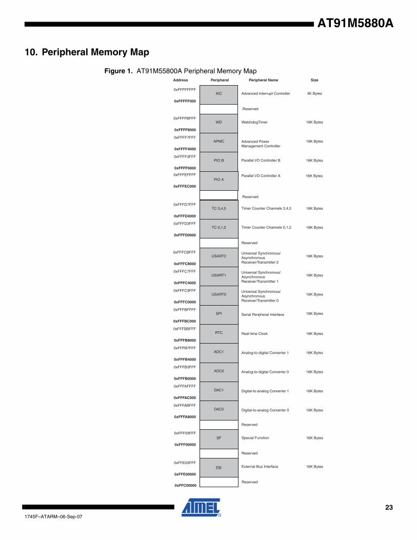
10. Peripheral Memory Map
Figure 1. AT91M55800A Peripheral Memory MapAddress Peripheral Peripheral Name Size
0xFFFFFFFF
0xFFFFF000
0xFFFFBFFF
0xFFFF8000
0xFFFF7FFF
0xFFFF4000
0xFFFF3FFF
0xFFFF0000
0xFFFD7FFF
0xFFFD4000
0xFFFC7FFF
0xFFFC4000
0xFFFCBFFF
0xFFFC8000
AIC
WD
APMC
PIO B
TC 3,4,5
USART1
USART2
SF
EBI
Advanced Interrupt Controller
WatchdogTimer
Advanced Power Management Controller
Parallel I/O Controller B
Parallel I/O Controller A
Timer Counter Channels 3,4,5
Universal Synchronous/Asynchronous Receiver/Transmitter 1
Universal Synchronous/Asynchronous Receiver/Transmitter 2
Reserved
Special Function
External Bus Interface
4K Bytes
16K Bytes
16K Bytes
16K Bytes
16K Bytes
16K Bytes
16K Bytes
16K Bytes
16K Bytes
Reserved
Reserved
PIO A
Reserved
0xFFFD3FFF
0xFFFD0000
TC 0,1,2 Timer Counter Channels 0,1,2 16K Bytes
0xFFFC3FFF
0xFFFC0000
USART0Universal Synchronous/Asynchronous Receiver/Transmitter 0
16K Bytes
0xFFFBBFFF
0xFFFB8000
0xFFFBFFFF
0xFFFBC000
RTC
SPI
Real-time Clock
Serial Peripheral Interface
16K Bytes
16K Bytes
0xFFFB7FFF
0xFFFB4000
ADC1 Analog-to-digital Converter 1 16K Bytes
0xFFFAFFFF
0xFFFAC000
0xFFFB3FFF
0xFFFB0000
DAC1
ADC0
Digital-to-analog Converter 1
Analog-to-digital Converter 0
16K Bytes
16K Bytes
0xFFFABFFF
0xFFFA8000
DAC0 Digital-to-analog Converter 0 16K Bytes
0xFFF03FFF
0xFFF00000
0xFFE03FFF
0xFFE00000
0xFFFEFFFF
0xFFFEC000
Reserved0xFFC00000
16K Bytes
Reserved
231745F–ATARM–06-Sep-07
11. EBI: External Bus Interface The EBI generates the signals that control the access to the external memory or peripheraldevices. The EBI is fully-programmable and can address up to 128M bytes. It has eight chipselects and a 24-bit address bus.
The 16-bit data bus can be configured to interface with 8- or 16-bit external devices. Separateread and write control signals allow for direct memory and peripheral interfacing.
The EBI supports different access protocols allowing single-clock cycle memory accesses.
The main features are:
• External memory mapping
• 8 active-low chip select lines
• 8- or 16-bit data bus
• Byte-write or byte-select lines
• Remap of boot memory
• Two different read protocols
• Programmable wait state generation
• External wait request
• Programmable data float time
The EBI User Interface is described on page 48.
241745F–ATARM–06-Sep-07
AT91M5880A

AT91M5880A
11.1 External Memory MappingThe memory map associates the internal 32-bit address space with the external 24-bit addressbus.
The memory map is defined by programming the base address and page size of the externalmemories (see EBI User Interface registers EBI_CSR0 to EBI_CSR7). Note that A0 - A23 is onlysignificant for 8-bit memory; A1 - A23 is used for 16-bit memory.
If the physical memory device is smaller than the programmed page size, it wraps around andappears to be repeated within the page. The EBI correctly handles any valid access to the mem-ory device within the page. (See Figure 11-1.)
In the event of an access request to an address outside any programmed page, an Abort signalis generated. Two types of Abort are possible: instruction prefetch abort and data abort. The cor-responding exception vector addresses are respectively 0x0000 000C and 0x0000 0010. It is upto the system programmer to program the error handling routine to use in case of an Abort (seethe ARM7TDMI datasheet for further information).
Figure 11-1. External Memory Smaller than Page Size
1-Mbyte Device
1-Mbyte Device
1-Mbyte Device
1-Mbyte Device
MemoryMap
Hi
Low
Hi
Low
Hi
Low
Hi
LowBase
Base + 1M Byte
Base + 2M Byte
Base + 3M Byte
Base + 4M Byte
Repeat 1
Repeat 2
Repeat 3
251745F–ATARM–06-Sep-07

11.2 EBI Pin Description
The following table shows how certain EBI signals are multiplexed:
Name Description Type
A0 - A23 Address bus (output) Output
D0 - D15 Data bus (input/output) I/O
NCS0 - NCS7 Active low chip selects (output) Output
NRD Read Enable (output) Output
NWR0 - NWR1 Lower and upper write enable (output) Output
NOE Output enable (output) Output
NWE Write enable (output) Output
NUB, NLB Upper and lower byte-select (output) Output
NWAIT Wait request (input) Input
Multiplexed Signals Functions
A0 NLB 8- or 16-bit data bus
NRD NOE Byte-write or byte-select access
NWR0 NWE Byte-write or byte-select access
NWR1 NUB Byte-write or byte-select access
261745F–ATARM–06-Sep-07
AT91M5880A

AT91M5880A
11.3 Data Bus WidthA data bus width of 8 or 16 bits can be selected for each chip select. This option is controlled bythe DBW field in the EBI_CSR (Chip-select Register) for the corresponding chip select.
Figure 11-2 shows how to connect a 512K x 8-bit memory on NCS2.
Figure 11-2. Memory Connection for an 8-bit Data Bus
Figure 11-3 shows how to connect a 512K x 16-bit memory on NCS2.
Figure 11-3. Memory Connection for a 16-bit Data Bus
11.4 Byte-write or Byte-select AccessEach chip select with a 16-bit data bus can operate with one of two different types of writeaccess:
• Byte-write Access supports two Byte-write and a single read signal.
• Byte-select Access selects upper and/or lower byte with two byte-select lines, and separate read and write signals.
This option is controlled by the BAT field in the EBI_CSR (Chip-select Register) for the corre-sponding chip select.
Byte-write Access is used to connect 2 x 8-bit devices as a 16-bit memory page.
• The signal A0/NLB is not used.
• The signal NWR1/NUB is used as NWR1 and enables upper byte writes.
• The signal NWR0/NWE is used as NWR0 and enables lower byte writes.
• The signal NRD/NOE is used as NRD and enables half-word and byte reads.
Figure 11-4 shows how to connect two 512K x 8-bit devices in parallel on NCS2.
EBI
D0 - D7
D8 - D15
A1 - A18
A0
NWR0
NRD
NCS2
D0 - D7
A1 - A18
A0
Write Enable
Output Enable
Memory Enable
NWR1
EBI
D0 - D7
D8 - D15
A1 - A19
NLB
NWE
NOE
NCS2
D0 - D7
D8 - D15
A0 - A18
Low Byte Enable
Write Enable
Output Enable
Memory Enable
NUB High Byte Enable
271745F–ATARM–06-Sep-07

Figure 11-4. Memory Connection for 2 x 8-bit Data Busses
Byte-select Access is used to connect 16-bit devices in a memory page.
• The signal A0/NLB is used as NLB and enables the lower byte for both read and write operations.
• The signal NWR1/NUB is used as NUB and enables the upper byte for both read and write operations.
• The signal NWR0/NWE is used as NWE and enables writing for byte or half word.
• The signal NRD/NOE is used as NOE and enables reading for byte or half word.
Figure 11-5 shows how to connect a 16-bit device with byte and half-word access (e.g. 16-bitSRAM) on NCS2.
Figure 11-5. Connection for a 16-bit Data Bus with Byte and Half-word Access
EBI
D0 - D7
D8 - D15
A1 - A19
A0
NWR0
NRD
NCS2
D0 - D7
A0 - A18
Write Enable
Read Enable
Memory Enable
NWR1
D8 - D15
A0 - A18
Write Enable
Read Enable
Memory Enable
EBI
D0 - D7
D8 - D15
A1 - A19
NLB
NWE
NOE
NCS2
D0 - D7
D8 - D15
A0 - A18
Low Byte Enable
Write Enable
Output Enable
Memory Enable
NUB High Byte Enable
281745F–ATARM–06-Sep-07
AT91M5880A

AT91M5880A
Figure 11-6 shows how to connect a 16-bit device without byte access (e.g. Flash) on NCS2.
Figure 11-6. Connection for a 16-bit Data Bus Without Byte-write Capability.
11.5 Boot on NCS0Depending on the device and the BMS pin level during the reset, the user can select either an 8-bit or 16-bit external memory device connected on NCS0 as the Boot Memory. In this case,EBI_CSR0 (Chip-select Register 0) is reset at the following configuration for chip select 0:
• 8 wait states (WSE = 1, NWS = 7)
• 8-bit or 16-bit data bus width, depending on BMS
Byte access type and number of data float time are respectively set to Byte-write Access and 0.With a nonvolatile memory interface, any value can be programmed for these parameters.
Before the remap command, the user can modify the chip select 0 configuration, programmingthe EBI_CSR0 with exact boot memory characteristics. The base address becomes effectiveafter the remap command, but the new number of wait states can be changed immediately. Thisis useful if a boot sequence needs to be faster.
EBI
D0 - D7
D8 - D15
A1 - A19
NLB
NWE
NOE
NCS2
D0 - D7
D8 - D15
A0 - A18
Write Enable
Output Enable
Memory Enable
NUB
291745F–ATARM–06-Sep-07

11.6 Read ProtocolsThe EBI provides two alternative protocols for external memory read access: standard and earlyread. The difference between the two protocols lies in the timing of the NRD (read cycle)waveform.
The protocol is selected by the DRP field in EBI_MCR (Memory Control Register) and is valid forall memory devices. Standard read protocol is the default protocol after reset.
Note: In the following waveforms and descriptions, NRD represents NRD and NOE since the two signals have the same waveform. Likewise, NWE represents NWE, NWR0 and NWR1 unless NWR0 and NWR1 are otherwise represented. ADDR represents A0 - A23 and/or A1 - A23.
11.6.1 Standard Read ProtocolStandard read protocol implements a read cycle in which NRD and NWE are similar. Both areactive during the second half of the clock cycle. The first half of the clock cycle allows time toensure completion of the previous access as well as the output of address and NCS before theread cycle begins.
During a standard read protocol, external memory access, NCS is set low and ADDR is valid atthe beginning of the access while NRD goes low only in the second half of the master clockcycle to avoid bus conflict (see Figure 11-7). NWE is the same in both protocols. NWE alwaysgoes low in the second half of the master clock cycle (see Figure 11-8).
Figure 11-7. Standard Read Protocol
11.6.2 Early Read ProtocolEarly read protocol provides more time for a read access from the memory by asserting NRD atthe beginning of the clock cycle. In the case of successive read cycles in the same memory,NRD remains active continuously. Since a read cycle normally limits the speed of operation ofthe external memory system, early read protocol can allow a faster clock frequency to be used.However, an extra wait state is required in some cases to avoid contentions on the external bus.
ADDR
NCS
NWE
MCK
NRD
or
301745F–ATARM–06-Sep-07
AT91M5880A

AT91M5880A
Figure 11-8. Early Read Protocol
11.6.3 Early Read Wait StateIn early read protocol, an early read wait state is automatically inserted when an external writecycle is followed by a read cycle to allow time for the write cycle to end before the subsequentread cycle begins (see Figure 11-9). This wait state is generated in addition to any other pro-grammed wait states (i.e. data float wait).
No wait state is added when a read cycle is followed by a write cycle, between consecutiveaccesses of the same type or between external and internal memory accesses.
Early read wait states affect the external bus only. They do not affect internal bus timing.
Figure 11-9. Early Read Wait State
ADDR
NCS
NWE
MCK
NRD
or
ADDR
NCS
NWE
MCK
Write Cycle Early Read Wait Read Cycle
NRD
311745F–ATARM–06-Sep-07

11.7 Write Data Hold TimeDuring write cycles in both protocols, output data becomes valid after the falling edge of theNWE signal and remains valid after the rising edge of NWE, as illustrated in the figure below.The external NWE waveform (on the NWE pin) is used to control the output data timing to guar-antee this operation.
It is therefore necessary to avoid excessive loading of the NWE pins, which could delay the writesignal too long and cause a contention with a subsequent read cycle in standard protocol.
Figure 11-10. Data Hold Time
In early read protocol the data can remain valid longer than in standard read protocol due to theadditional wait cycle which follows a write access.
ADDR
NWE
Data output
MCK
321745F–ATARM–06-Sep-07
AT91M5880A

AT91M5880A
11.8 Wait StatesThe EBI can automatically insert wait states. The different types of wait states are listed below:
• Standard wait states
• Data float wait states
• External wait states
• Chip select change wait states
• Early read wait states (as described in Read Protocols)
11.8.1 Standard Wait StatesEach chip select can be programmed to insert one or more wait states during an access on thecorresponding device. This is done by setting the WSE field in the corresponding EBI_CSR. Thenumber of cycles to insert is programmed in the NWS field in the same register.
Below is the correspondence between the number of standard wait states programmed and thenumber of cycles during which the NWE pulse is held low:
0 wait states 1/2 cycle
1 wait state 1 cycle
For each additional wait state programmed, an additional cycle is added.
Figure 11-11. One Wait State Access
Notes: 1. Early Read Protocol
2. Standard Read Protocol
11.8.2 Data Float Wait StateSome memory devices are slow to release the external bus. For such devices it is necessary toadd wait states (data float waits) after a read access before starting a write access or a readaccess to a different external memory.
The Data Float Output Time (tDF) for each external memory device is programmed in the TDFfield of the EBI_CSR register for the corresponding chip select. The value (0 - 7 clock cycles)indicates the number of data float waits to be inserted and represents the time allowed for thedata output to go high impedance after the memory is disabled.
ADDR
NCS
NWE
MCK
1 Wait State Access
NRD (1) (2)
331745F–ATARM–06-Sep-07
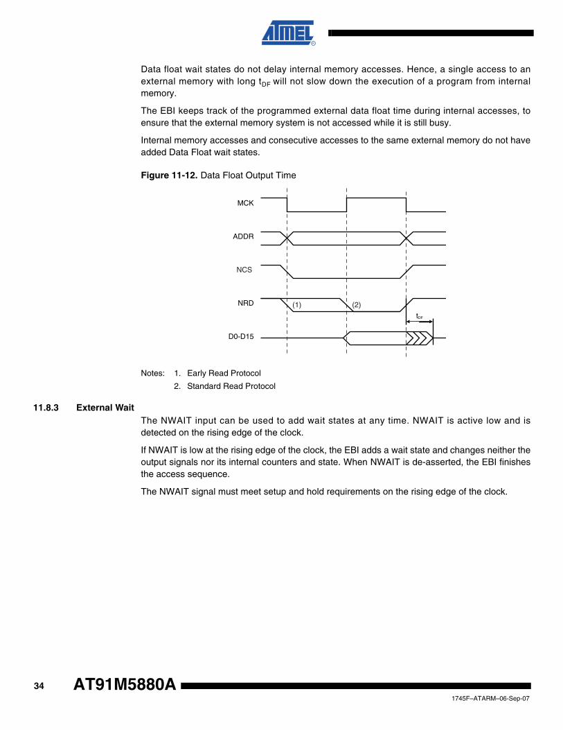
Data float wait states do not delay internal memory accesses. Hence, a single access to anexternal memory with long tDF will not slow down the execution of a program from internalmemory.
The EBI keeps track of the programmed external data float time during internal accesses, toensure that the external memory system is not accessed while it is still busy.
Internal memory accesses and consecutive accesses to the same external memory do not haveadded Data Float wait states.
Figure 11-12. Data Float Output Time
Notes: 1. Early Read Protocol
2. Standard Read Protocol
11.8.3 External WaitThe NWAIT input can be used to add wait states at any time. NWAIT is active low and isdetected on the rising edge of the clock.
If NWAIT is low at the rising edge of the clock, the EBI adds a wait state and changes neither theoutput signals nor its internal counters and state. When NWAIT is de-asserted, the EBI finishesthe access sequence.
The NWAIT signal must meet setup and hold requirements on the rising edge of the clock.
ADDR
NRD
D0-D15
MCK
tDF
(1) (2)
NCS
341745F–ATARM–06-Sep-07
AT91M5880A

AT91M5880A
Figure 11-13. External Wait
Notes: 1. Early Read Protocol
2. Standard Read Protocol
11.8.4 Chip Select Change Wait StatesA chip select wait state is automatically inserted when consecutive accesses are made to twodifferent external memories (if no wait states have already been inserted). If any wait stateshave already been inserted, (e.g., data float wait) then none are added.
Figure 11-14. Chip Select Wait
Notes: 1. Early Read Protocol
2. Standard Read Protocol
ADDR
NCS
NWE
MCK
NRD(1) (2)
NWAIT
NCS1
NCS2
MCK
Mem 1 Chip Select Wait Mem 2
NRD
NWE
(1) (2)
351745F–ATARM–06-Sep-07

11.9 Memory Access WaveformsFigure 11-15 through Figure 11-18 show examples of the two alternative protocols for externalmemory read access.
Figure 11-15. Standard Read Protocol with no tDF
Rea
d M
em 1
Writ
e M
em 1
Rea
d M
em 1
Rea
d M
em 2
Writ
e M
em 2
Rea
d M
em 2
Chi
p S
elec
t C
hang
e W
ait
A0
- A
23
NR
D
NW
E
NC
S1
NC
S2
D0
- D
15 (
Mem
1)
D0
- D
15 (
Mem
2)
D0
- D
15 (
AT
91)
MC
K
t WH
DX
t WH
DX
361745F–ATARM–06-Sep-07
AT91M5880A

AT91M5880A
Figure 11-16. Early Read Protocol with no tDF
Rea
d M
em 1
Writ
e M
em 1
A0
- A
23
NR
D
NW
E
NC
S1
NC
S2
D0
- D
15 (
Mem
1)
D0
- D
15 (
Mem
2)
D0
- D
15 (
AT
91)
MC
K
Ear
ly R
ead
Wai
t Cyc
leR
ead
Mem
1R
ead
Mem
2W
rite
Mem
2E
arly
Rea
dW
ait C
ycle
Rea
d M
em 2
Chi
p S
elec
tC
hang
e W
ait
Long
t WH
DX
Long
t WH
DX
371745F–ATARM–06-Sep-07

Figure 11-17. Standard Read Protocol with tDF
Rea
d M
em 1
Writ
e M
em 1
A0
- A
23
NR
D
NW
E
NC
S1
NC
S2
D0
- D
15 (
Mem
1)
D0
- D
15 (
Mem
2)
D0
- D
15 (
AT
91)
MC
K
Dat
aF
loat
Wai
t
Rea
d M
em 1 Dat
aF
loat
Wai
t
Rea
d M
em 2
Rea
d M
em 2 Dat
aF
loat
Wai
t
Writ
e M
em 2
Writ
e M
em 2
Writ
e M
em 2
t WH
DX
t DF
t DF
t DF
381745F–ATARM–06-Sep-07
AT91M5880A

AT91M5880A
Figure 11-18. Early Read Protocol with tDF
Rea
d M
em 1
Writ
e M
em 1
A0
- A
23
NR
D
NW
E
NC
S1
NC
S2
D0
- D
15 (
Mem
1)
D0
- D
15 (
Mem
2)
D0
- D
15 (
AT
91)
MC
K
Dat
a F
loat
Wai
t
Ear
lyR
ead
Wai
tR
ead
Mem
1 Dat
a F
loat
Wai
t
Rea
d M
em 2
Rea
d M
em 2 Dat
a F
loat
Wai
t
Writ
e M
em 2
Writ
e M
em 2
Writ
e M
em 2
t DF
t DF
t DF
t WH
DX
391745F–ATARM–06-Sep-07

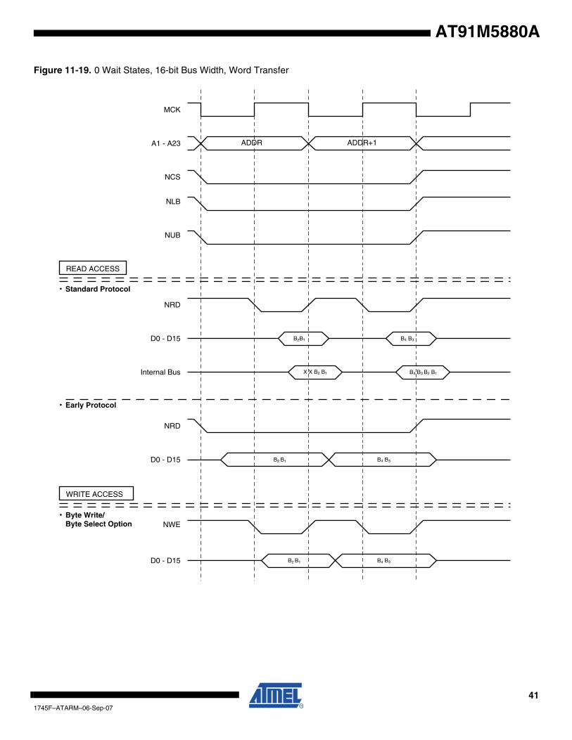
Figure 11-19 through Figure 11-25 show the timing cycles and wait states for read and writeaccess to the various AT91M55800A external memory devices. The configurations describedare as follows:
Table 11-1. Memory Access Waveforms
Figure Number Number of Wait States Bus Width Size of Data Transfer
11-19 0 16 Word
11-20 1 16 Word
11-21 1 16 Half-word
11-22 0 8 Word
11-23 1 8 Half-word
11-24 1 8 Byte
11-25 0 16 Byte
401745F–ATARM–06-Sep-07
AT91M5880A
AT91M5880A
Figure 11-19. 0 Wait States, 16-bit Bus Width, Word Transfer
ADDR ADDR+1
B2B1 B4 B3
B4 B3 B2 B1
MCK
A1 - A23
NCS
NRD
D0 - D15
Internal Bus X X B2 B1
READ ACCESS
NRD
B2 B1 B4 B3 D0 - D15
WRITE ACCESS
NWE
B2 B1 B4 B3 D0 - D15
NLB
NUB
· Standard Protocol
· Early Protocol
· Byte Write/ Byte Select Option
411745F–ATARM–06-Sep-07

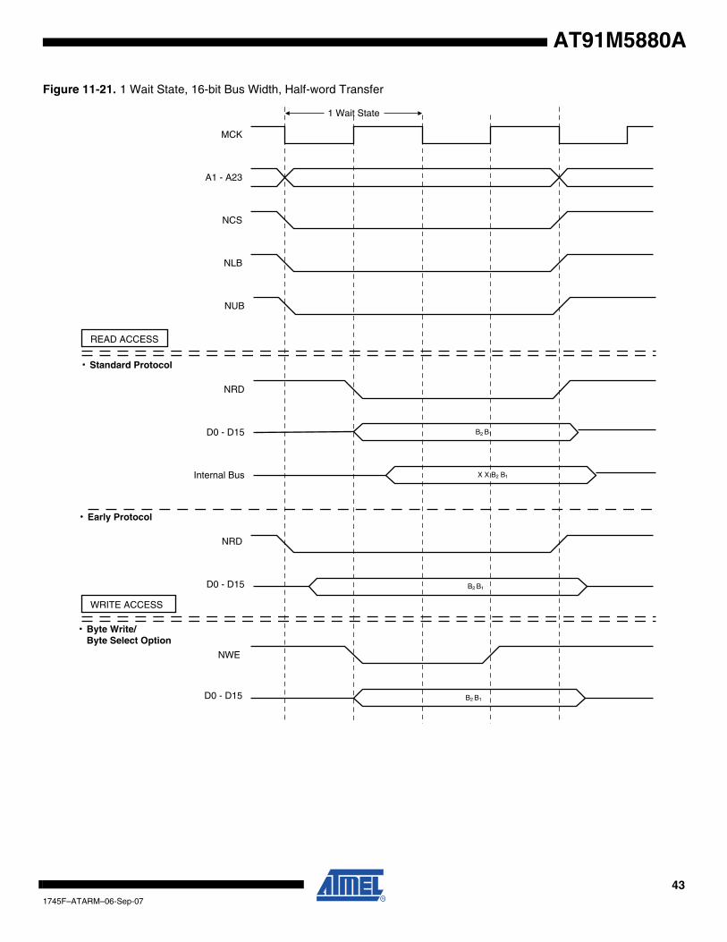
Figure 11-20. 1 Wait State, 16-bit Bus Width, Word Transfer
ADDR ADDR+1
B2B1
B4 B3
X X B2 B1 B4 B3 B2 B1
1 Wait State 1 Wait State
MCK
A1 - A23
NCS
NRD
D0 - D15
Internal Bus
WRITE ACCESS
READ ACCESS
NRD
D0 - D15
· Standard Protocol
· Early Protocol
B4B3
NWE
D0 - D15 B2B1 B4B3
NLB
NUB
B2 B1
· Byte Write/ Byte Select Option
421745F–ATARM–06-Sep-07
AT91M5880A
AT91M5880A
Figure 11-21. 1 Wait State, 16-bit Bus Width, Half-word Transfer
B2 B1
1 Wait State
MCK
A1 - A23
NCS
NRD
D0 - D15
Internal Bus X X B2 B1
READ ACCESS
· Standard Protocol
NLB
NUB
· Early Protocol
B2 B1
NRD
D0 - D15
WRITE ACCESS
NWE
B2 B1D0 - D15
· Byte Write/ Byte Select Option
431745F–ATARM–06-Sep-07

Figure 11-22. 0 Wait States, 8-bit Bus Width, Word Transfer
ADDR ADDR+1
X B1
X B3 B2 B1
MCK
A0 - A23
NCS
NRD
D0 - D15
Internal Bus
ADDR+2 ADDR+3
X X B2 B1
X B2
X X X B1
X B3 X B4
B4 B3 B2 B1
READ ACCESS
· Standard Protocol
· Early Protocol
NRD
X B1D0 - D15 X B2 X B3 X B4
WRITE ACCESS
NWR0
NWR1
X B1D0 - D15 X B2 X B3 X B4
441745F–ATARM–06-Sep-07
AT91M5880A

AT91M5880A
Figure 11-23. 1 Wait State, 8-bit Bus Width, Half-word Transfer
ADDR
X B1
1 Wait State
MCK
A0 - A23
NCS
NRD
D0 - D15
Internal Bus
ADDR+1
1 Wait State
X X B2 B1
X B2
X X X B1
READ ACCESS
· Standard Protocol
· Early Protocol
NRD
X B1D0 - D15 X B2
WRITE ACCESS
NWR0
X B1D0 - D15 X B2
NWR1
451745F–ATARM–06-Sep-07

Figure 11-24. 1 Wait State, 8-bit Bus Width, Byte Transfer
XB1
1 Wait State
MCK
A0 - A23
NCS
NRD
D0-D15
Internal Bus X X X B1
READ ACCESS
· Standard Protocol
· Early Protocol
D0 - D15 X B1
WRITE ACCESS
NWR0
D0-D15 X B1
NRD
NWR1
461745F–ATARM–06-Sep-07
AT91M5880A

AT91M5880A
Figure 11-25. 0 Wait States, 16-bit Bus Width, Byte Transfer
MCK
A1-A23
NCS
NWR1
D0-D15 X B1 B2X
ADDR X X X 0 ADDR X X X 0
ADDR X X X 0 ADDR X X X 1Internal Address
Internal Bus X X X B1 X X B2X
NLB
NUB
READ ACCESS
· Standard Protocol
NRD
· Early Protocol
NRD
D0-D15 XB1 B2X
WRITE ACCESS
NWR0
D0-D15 B1B1 B2B2
· Byte Write Option
· Byte Select Option
NWE
471745F–ATARM–06-Sep-07

11.10 EBI User InterfaceThe EBI is programmed using the registers listed in the table below. The Remap Control Regis-ter (EBI_RCR) controls exit from Boot Mode (see Section 11.5 “Boot on NCS0” on page 29) TheMemory Control Register (EBI_MCR) is used to program the number of active chip selects anddata read protocol. Eight Chip-select Registers (EBI_CSR0 to EBI_CSR7) are used to programthe parameters for the individual external memories. Each EBI_CSR must be programmed witha different base address, even for unused chip selects.
Base Address: 0xFFE00000 (Code Label EBI_BASE)
Notes: 1. 8-bit boot (if BMS is detected high)
2. 16-bit boot (if BMS is detected low)
Table 11-2. Register Mapping
Offset Register Name Access Reset
0x00 Chip-select Register 0 EBI_CSR0 Read/Write0x0000203E(1)
0x0000203D(2)
0x04 Chip-select Register 1 EBI_CSR1 Read/Write 0x10000000
0x08 Chip-select Register 2 EBI_CSR2 Read/Write 0x20000000
0x0C Chip-select Register 3 EBI_CSR3 Read/Write 0x30000000
0x10 Chip-select Register 4 EBI_CSR4 Read/Write 0x40000000
0x14 Chip-select Register 5 EBI_CSR5 Read/Write 0x50000000
0x18 Chip-select Register 6 EBI_CSR6 Read/Write 0x60000000
0x1C Chip-select Register 7 EBI_CSR7 Read/Write 0x70000000
0x20 Remap Control Register EBI_RCR Write-only –
0x24 Memory Control Register EBI_MCR Read/Write 0
481745F–ATARM–06-Sep-07
AT91M5880A

AT91M5880A
11.10.1 EBI Chip Select RegisterRegister Name: EBI_CSR0 - EBI_CSR7
Access Type: Read/Write
Reset Value: See Table 11-2
Absolute Address: 0xFFE00000 - 0xFFE0001C
• DBW: Data Bus Width
• NWS: Number of Wait StatesThis field is valid only if WSE is set.
• WSE: Wait State Enable (Code Label EBI_WSE)0 = Wait state generation is disabled. No wait states are inserted.
1 = Wait state generation is enabled.
31 30 29 28 27 26 25 24
BA
23 22 21 20 19 18 17 16
BA – – – –
15 14 13 12 11 10 9 8
– – CSEN BAT TDF PAGES
7 6 5 4 3 2 1 0
PAGES – WSE NWS DBW
DBW Data Bus Width
Code Label
EBI_DBW
0 0 Reserved –
0 1 16-bit data bus width EBI_DBW_16
1 0 8-bit data bus width EBI_DBW_8
1 1 Reserved –
NWS Number of Standard Wait States
Code Label
EBI_NWS
0 0 0 1 EBI_NWS_1
0 0 1 2 EBI_NWS_2
0 1 0 3 EBI_NWS_3
0 1 1 4 EBI_NWS_4
1 0 0 5 EBI_NWS_5
1 0 1 6 EBI_NWS_6
1 1 0 7 EBI_NWS_7
1 1 1 8 EBI_NWS_8
491745F–ATARM–06-Sep-07

• PAGES: Page Size
• TDF: Data Float Output Time
• BAT: Byte Access Type
• CSEN: Chip Select Enable (Code Label EBI_CSEN)0 = Chip select is disabled.
1 = Chip select is enabled.
• BA: Base Address (Code Label EBI_BA)These bits contain the highest bits of the base address. If the page size is larger than 1M byte, the unused bits of the baseaddress are ignored by the EBI decoder.
PAGES Page Size Active Bits in Base Address
Code Label
EBI_PAGES
0 0 1M Byte 12 Bits (31-20) EBI_PAGES_1M
0 1 4M Bytes 10 Bits (31-22) EBI_PAGES_4M
1 0 16M Bytes 8 Bits (31-24) EBI_PAGES_16M
1 1 64M Bytes 6 Bits (31-26) EBI_PAGES_64M
TDF Number of Cycles Added after the Transfer
Code Label
EBI_TDF
0 0 0 0 EBI_TDF_0
0 0 1 1 EBI_TDF_1
0 1 0 2 EBI_TDF_2
0 1 1 3 EBI_TDF_3
1 0 0 4 EBI_TDF_4
1 0 1 5 EBI_TDF_5
1 1 0 6 EBI_TDF_6
1 1 1 7 EBI_TDF_7
BAT Selected BAT
Code Label
EBI_BAT
0 Byte-write access type EBI_BAT_BYTE_WRITE
1 Byte-select access type EBI_BAT_BYTE_SELECT
501745F–ATARM–06-Sep-07
AT91M5880A

AT91M5880A
11.10.2 EBI Remap Control RegisterRegister Name: EBI_RCR
Access Type: Write-only
Absolute Address: 0xFFE00020
Offset: 0x20
• RCB: Remap Command Bit (Code Label EBI_RCB)0 = No effect.
1 = Cancels the remapping (performed at reset) of the page zero memory devices.
11.10.3 EBI Memory Control RegisterRegister Name: EBI_MCR
Access Type: Read/Write
Reset Value: 0
Absolute Address: 0xFFE00024
Offset: 0x24
• DRP: Data Read Protocol
31 30 29 28 27 26 25 24
– – – – – – – –
23 22 21 20 19 18 17 16
– – – – – – – –
15 14 13 12 11 10 9 8
– – – – – – – –
7 6 5 4 3 2 1 0
– – – – – – – RCB
31 30 29 28 27 26 25 24
– – – – – – – –
23 22 21 20 19 18 17 16
– – – – – – – –
15 14 13 12 11 10 9 8
– – – – – – – –
7 6 5 4 3 2 1 0
– – – DRP – – – –
DRP Selected DRP
Code Label
EBI_DRP
0 Standard read protocol for all external memory devices enabled EBI_DRP_STANDARD
1 Early read protocol for all external memory devices enabled EBI_DRP_EARLY
511745F–ATARM–06-Sep-07

12. APMC: Advanced Power Management ControllerThe AT91M55800A features an Advanced Power Management Controller, which optimizes boththe power consumption of the device and the complete system. The APMC controls the clockingelements such as the oscillators and the PLL, the core and the peripheral clocks, and has thecapability to control the system power supply.
Main Power is used throughout this document to identify the voltages powering theAT91M55800A and other components of the system, with the exception of the Battery Backupvoltage, which is applied to the VDDBU. Main Power supplies VDDIO, VDDCORE and, ifrequired, the analog voltage VDDA. A battery or battery capacitor generally supplies the BatteryBackup Power.
The APMC consists of the following elements:
• The RTC Oscillator, which provides the Slow Clock at 32768 Hz.
• The Main Oscillator, which provides a clock that depends on the frequency of the crystal connected to the XIN and XOUT pins.
• The Phase Lock Loop.
• The ARM Core Clock Controller, which allows entry to the Idle Mode.
• The Peripheral Clock Controller, which conserves the power consumption of unused peripherals.
• The Master Clock Output Controller.
• The Shut-down Logic, which controls the Main Power.
Figure 12-1. APMC Module
Note: The RTC peripheral is described in a separate section.
Advanced Peripheral Bus
IRQControlPLL TimerOSC Timer
PLL Main OSC
DeviceClock Control
RTC (1)RTCOSC
Reset Control
Shut-down Logic
APMC
VDDIO/VDDCORE
VDDBU
WAKEUP
NRSTBU
XIN32XOUT32
XIN
XOUT
SHDN
APMCIRQ
Arm Clock
Peripheral Clocks0
ARM Interrupt (IRQ and FIQ)
n
Alarm
SLCKIRQ
Slow Clock_SLCK
521745F–ATARM–06-Sep-07
AT91M5880A

AT91M5880A
12.1 Operating ModesFive operating modes are supported by the APMC and offer different power consumption levelsand event response latency times.
• Normal Mode:
The Main Power supply is switched on; the ARM Core Clock is enabled and the peripheralclocks are enabled according to the application requirements.
• Idle Mode:
The Main Power is switched on; the ARM Core Clock is disabled and waiting for the nextinterrupt (or a main reset); the peripheral clocks are enabled according to the applicationrequirements and the PDC transfers are still possible.
• Slow Clock Mode:
Similar to Normal Mode, but the Main Oscillator and the PLL are switched off to save power;the device core and peripheral run in Slow Clock Mode; Note that Slow Clock Mode is themode selected after the reset.
• Standby Mode:
A combination of the Slow Clock Mode and the Idle Mode, which enables the processor torespond quickly to a wake-up event by keeping very low power consumption.
• Power-down Mode:
The Main Power supply is turned off at the external power source until a programmableedge on the wake-up signal or a programmable RTC Alarm occurs.
531745F–ATARM–06-Sep-07
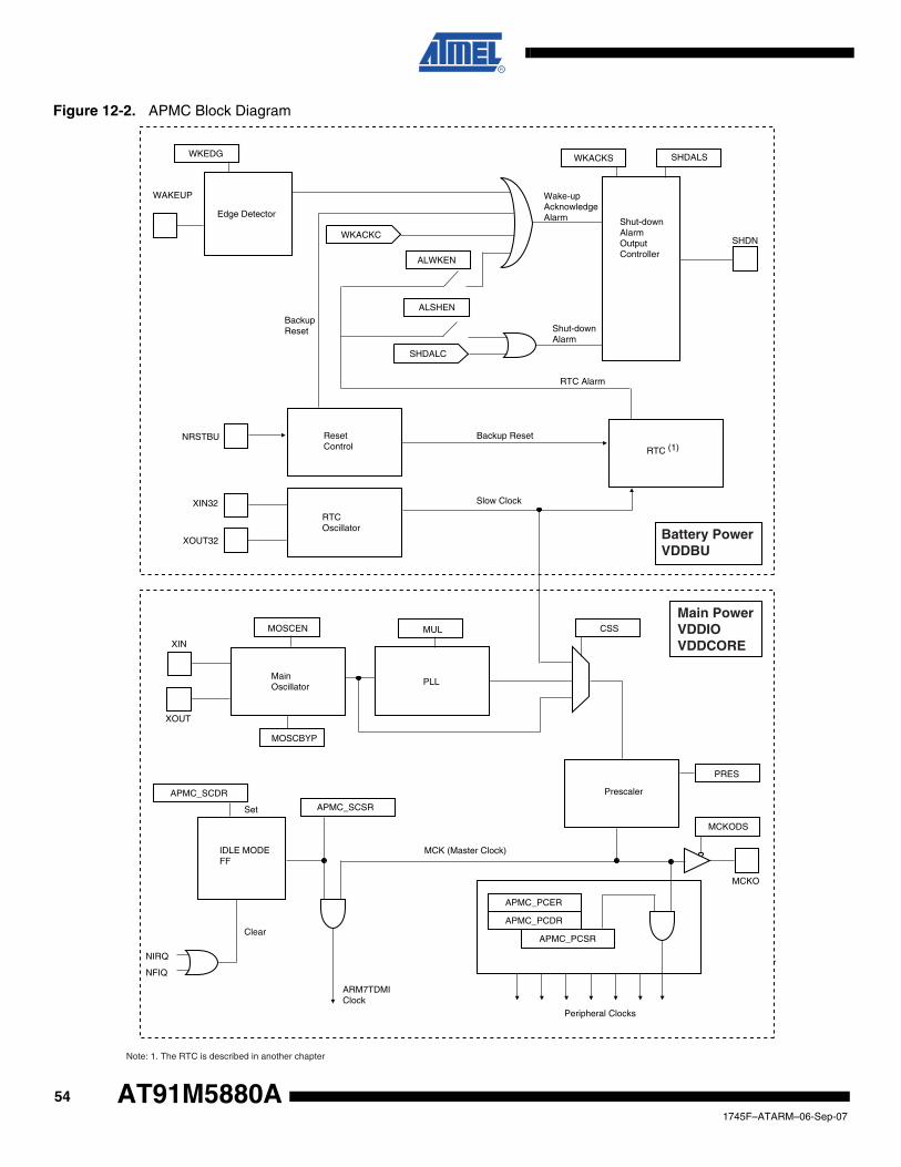
Figure 12-2. APMC Block Diagram
ARM7TDMIClock
NIRQ
NFIQ
IDLE MODEFF
APMC_SCDR
APMC_SCSR
MCK (Master Clock)
Prescaler
Peripheral Clocks
Clear
Set
XIN
XOUT
MCKO
MCKODS
PRES
APMC_PCER
APMC_PCDR
APMC_PCSR
MOSCBYP
MULMOSCEN CSS
PLLMainOscillator
ResetControl
RTCOscillator
RTC (1)Backup Reset
Slow Clock
RTC Alarm
Shut-down Alarm
BackupReset
Wake-up Acknowledge Alarm Shut-down
Alarm Output Controller
SHDN
WKACKS SHDALSWKEDG
WAKEUP
Edge Detector
WKACKC
ALWKEN
ALSHEN
SHDALC
NRSTBU
XIN32
XOUT32 Battery PowerVDDBU
Main PowerVDDIOVDDCORE
Note: 1. The RTC is described in another chapter
541745F–ATARM–06-Sep-07
AT91M5880A

AT91M5880A
12.2 Slow Clock GeneratorThe AT91M55800A has a very low power 32 kHz oscillator powered by the backup battery volt-age supplied on the VDDBU pins. The XIN32 and XOUT32 pins must be connected to a 32768Hz crystal. The oscillator has been especially designed to connect to a 6 pF typical load capaci-tance crystal and does not require any external capacitor, as it integrates the XIN32 andXOUT32 capacitors to ground. For a higher typical load capacitance, two external capacitancesmust be wired as shown in Figure 12-3:
Figure 12-3. Higher Typical Load Capacitance
12.2.1 Backup Reset Controller
The backup reset controller initializes the logic supplied by the backup battery power. A simpleRC circuit connected to the NRSTBU pin provides a power-on reset signal to the RTC and theshutdown logic. When the reset signal increases and as the startup time of the 32 kHz oscillatoris around 300 ms, the AT91M55800A maintains the internal backup reset signal for 32768 oscil-lator clock cycles in order to guarantee the backup power supplied logic does not operate beforethe oscillator output is stabilized.Alternatively, a reset supervisor can be connected to the NRSTBU pin in place of the RC.
12.2.2 Slow Clock
The Slow Clock is the only clock considered permanent in an AT91M55800A-based system andis essential in the operations of the APMC (Advanced Power Management Controller). In anyuse-case, a 32768 Hz crystal must be connected to the XIN32 and XOUT32 pins in order toensure that the Slow Clock is present.
XIN32 XOUT32 GNDPLL
CL2CL1
551745F–ATARM–06-Sep-07

12.3 Clock GeneratorThe clock generator consists of the main oscillator, the PLL and the clock selection logic with itsprescaler. It aims at selecting the Master Clock, called MCK throughout this datasheet. Theclock generator also contains the circuitry needed to drive the MCKO pin with the master clocksignal.
12.3.1 Main OscillatorThe Main Oscillator is designed for a 3 to 20 MHz fundamental crystal. The typical crystal con-nection is illustrated in Figure 12-4. The 1 kΩ resistor is only required for crystals withfrequencies lower than 8 MHz. The oscillator contains 25 pF capacitances on each XIN andXOUT pin. Consequently, CL1 and CL2 can be removed when a crystal with a load capacitanceof 12.5 pF is used.
Figure 12-4. Typical Crystal Connection of Main Oscillator
The Main Oscillator can be bypassed if the MOSCBYP bit in the Clock Generator Mode Register(APMC_CGMR) is set to 1. In this case, any frequency (up to the maximum specified in the elec-trical characteristics datasheet) can be input on the XIN pin. If the PLL is used, a minimum inputfrequency is required.
To minimize the power required to start up the system, the Main Oscillator is disabled after thereset. The software can deactivate the Main Oscillator to reduce the power consumption byclearing the MOSCEN bit in APMC_CGMR. The MOSCS (Main Oscillator Status) bit inAPMC_SR is automatically cleared, indicating that the Main Oscillator is off.
Writing the MOSCEN bit in APMC_CGMR reactivates the Main Oscillator and loads the valuewritten in the OSCOUNT field in APMC_CGMR in the oscillator counter. Then, the oscillatorcounter decrements every 8 clock cycles and when it reaches 0, the MOSCS bit is set and canprovide an interrupt.
12.3.2 Phase Lock Loop
The Main Oscillator output signal feeds the phase lock loop, which aims at multiplying the fre-quency of its input signal by a number up to 64. This number is programmed in the MUL field ofAPMC_CGMR and the multiplication ratio is the programmed value plus one (MUL+1). If a nullvalue is programmed into MUL, the PLL is automatically disabled to save power.
The PLL is disabled at reset to minimize the power consumption.
A start-up sequence must be executed to enable the PLL if it is disabled. This sequence isstarted by writing a new MUL value in APMC_CGMR. This automatically clears the LOCK bit inAPMC_SR and loads the PLL counter with the value programmed in the PLLCOUNT field. Then,the PLL counter decrements at each Slow Clock cycle.
XIN XOUT GNDPLL
CL2CL1
1KΩ
561745F–ATARM–06-Sep-07
AT91M5880A

AT91M5880A
Note: Programming one in PLLCOUNT is the minimum allowed and guarantees at least 2 Slow Clock cycles before the lock bit is set. Programming n in PLLCOUNT guarantees (n+1) the delay of Slow Clock cycles. When the PLL Counter reaches 0, the LOCK bit in APMC_SR is set and can cause an interrupt. Programming MUL or PLLCOUNT before the LOCK bit is set may lead to unpredict-able behavior.
If the PLL multiplication is changed while the PLL is already active, the LOCK bit in APMC_SR isautomatically cleared and the same sequence is restarted. The PLL is automatically bypassedwhile the frequency is changing (while LOCK is 0). If the Main Oscillator is reactivated at thesame time the PLL is enabled, the LOCK bit is set only when both the Main Oscillator and thePLL are stabilized.
12.3.3 PLL Filter
The Phase Lock Loop has a dedicated PLLRC pin which must connect with an appropriate sec-ond order filter made up of one resistor and two capacitors. If the integrated PLL is not used, itcan remain disabled. The PLLRC pin must be grounded if the resistor and the capacitors need tobe saved. The following figure shows a typical filter connection.
Figure 12-5. Typical Filter Connection
In order to obtain optimal results with a 16 MHz input frequency and a 32 MHz output frequency,the typical component values for the PLL filter are:
R = 287Ω - C1 = 680 nF - C2 = 68 nF
The lock time with these values is about 3.5 µs in this example.
12.3.4 Master Clock Selection
The MCK (Master Clock) can be selected through the CSS field in APMC_CGMR between theSlow Clock, the output of the Main Oscillator or the output of the PLL.
The following CSS field definitions are forbidden and the write operations are not taken intoaccount by the APMC:
• deselect the Slow Clock if the Main Oscillator is disabled or its output is not stabilized
• disable the PLL without having first selected the Slow Clock or the Main Oscillator clock
• select the PLL clock and, in the same register, write disable the PLL
• select either the Main Oscillator or the PLL clocks and, in the same register, write disable the Main Oscillator
• disable the Main Oscillator without having first selected the Slow Clock
This clock switch is performed in some Slow Clocks and PLLs or Main Oscillator clock cycles asdescribed in the state machine diagram below:
GNDPLL
C2
C1
R
PLLRC
571745F–ATARM–06-Sep-07

Figure 12-6. Clock Switch
12.3.5 Slow Clock InterruptThe APMC also features the Slow Clock interrupt, allowing the user to detect when the MasterClock is actually switched to the Slow Clock. Switching from the Slow Clock to a higher fre-quency is generally performed safely, as the processor is running slower than the targetfrequency. However, switching from a high frequency to the Slow Clock requires the high fre-quency to be valid during the switch time. The Slow Clock interrupt permits the user to knowexactly when the switch has been achieved, thus, when the Main Oscillator or the PLL can bedisabled.
12.3.6 PrescalerThe prescaler is the last stage to provide the master clock. It permits the selected clock to bedivided by a power of 2 between 1 and 64. The default value is 1 after the reset. The prescalerallows the microcontroller operating frequency to reach down to 512 Hz.
Precautions must be taken when defining a master clock lower than the Slow Clock, as someperipherals (RTC and APMC) can still operate at Slow Clock frequency. In this case, access tothe peripheral registers that are updated at 32 kHz cannot be ensured.
12.3.7 Master Clock OutputThe Master Clock can be output to the MCKO pad. The MCKO pad can be tri-stated to minimizepower consumption by setting the bit MCKODS (Master Clock Output Disable) in APMC_CGMR(default is MCKO enabled).
Slow Clock Mode
PLL Clock ModeOscillator Clock Mode
5 SLCK Cycles
4 SLCK Cycles+
3 PLL Clock Cycles 5 SLCK Cycles3 SLCK Cycles+
3 Oscillator Clock Cycles
5 SLCK Cycles+
3 PLL Clock Cycles
4 SLCK Cycles+
3 Oscillator Clock Cycles
7 SLCK Cycles+
3 PLL Clock Cycles
581745F–ATARM–06-Sep-07
AT91M5880A

AT91M5880A
12.4 System ClockThe AT91M55800A has only one system clock: the ARM Core clock. It can be enabled and dis-abled by writing to the System Clock Enable (APMC_SCER) and System Clock DisableRegisters (APMC_SCDR). The status of the ARM Core clock (at least for debug purposes) canbe read in the System Clock Status Register (APMC_SCSR).
The ARM Core clock is enabled after a reset and is automatically re-enabled by any enabledinterrupt.
When the ARM Core clock is disabled, the current instruction is finished before the clock isstopped.
Note: Stopping the ARM Core does not prevent PDC transfers.
12.5 Peripheral ClocksEach peripheral clock integrated in the AT91M55800A can be individually enabled and disabledby writing to the Peripheral Clock Enable (APMC_PCER) and Peripheral Clock Disable(APMC_PCDR) Registers. The status of the peripheral clocks can be read in the PeripheralClock Status Register (APMC_PCSR).
When a peripheral clock is disabled, the clock is immediately stopped. When the clock is re-enabled, the peripheral resumes action where it left off.
In order to stop a peripheral, it is recommended that the system software waits until the periph-eral has executed its last programmed operation before disabling the clock. This is to avoid datacorruption or erroneous behavior of the system.
The peripheral clocks are automatically disabled after a reset.
The bits that control the peripheral clocks are the same as those that control the InterruptSources in the AIC.
12.6 Shut-down and Wake-upThe APMC (Advanced Power Management Controller) integrates shut-down and wake-up logicto control an external main power supply. This logic is supplied by the Battery Backup Power.This feature makes the Power-down mode possible.
If the SHDN pin is connected to the shut-down pin of the main power supply, the Shut-downcommand (SHDALC) in APMC_PCR disables the main power. The shut-down input of the con-verter is generally pulled up or down by a resistor, depending on its active level.
There are 3 ways to exit Power-down mode and restart the main power:
• An alarm programmed in the RTC occurs and the bit ALWKEN in APMC_PMR is set.
• An edge defined by the field WKEDG in APMC_PMR occurs on the pin WAKEUP.
• The user opens the Shut-down line with an external jumper or push-button.
Figure 12-7 shows a typical application using the Shut-down and Wake-up features.
591745F–ATARM–06-Sep-07

Figure 12-7. Shut-down and Wake-up Features
To accommodate the different types of main power supply available, and different signals thatcan command the shut-down of this device, tri-state, level 0 and level 1 are user-definable forthe Shut-down pin. The Wake-up pin can be configured as detected on the positive or negativeedge, and at high or low level. They are selected by the SHDALS and WKACKS fields inAPMC_PMR.
12.7 Alarm If the Shut-down feature is not used, the pin SHDN can be used as an Alarm Output Signal fromthe RTC Alarm. The Alarm State corresponds to Shut-down, and the Acknowledge or Non-AlarmState corresponds to Wake-up.
The alarm control logic is the same as that for Shut-down. The SHDALC command inAPMC_PCR (defined by the field SHDALS in APMC_PMR) and the WKACKS command inAPMC_PCR (defined by the field WKACKS field in APMC_PMR) control the SHDN pin.
The alarm can be positioned by an RTC Alarm and be acknowledged by a programmable edgeon the WAKEUP pin. The Backup Reset initializes the logic in Non-Alarm State.
DC/DC ConverterPower Supply
VDDIO
VDDCORE
GND
VDDBU
NRSTBU
GNDBU
SHDN
WAKE-UP
AT91M55800
SHD
Shut-down Jumper Disable
Main Start Up
BatteryBackup -
+
Resistor required bysome DC/DCConverters
601745F–ATARM–06-Sep-07
AT91M5880A

AT91M5880A
12.8 First Start-up SequenceAt initial startup, or after VDDBU has been disconnected, the battery-supplied logic must beinitialized.
The Battery Backup Reset sets the following default state:
• Shut-down Logic
Initialized in the Wake-up state (or Non Alarm)
• The Power Mode Register
Shut-down defines SHDN as level 0 (SHDALS = 1)
Wake-up defines SHDN as tri-state (WKACKS = 0)
• The Real-time Clock Configuration and Data Registers
A simple RC network can be used as a power-on reset for the battery supply.
The pin SHDN is tri-stated by default. An external resistor must hold the main power supplyshut-down pin in the inactive state. The shut-down logic can be programmed with the correctactive level of the power supply shut-down input during the first start-up sequence.
The first time the system is powered up, the SHDN pin is tri-stated because different power sup-plies use different logic levels for their shut-down input signals. To minimize backup batterypower consumption, there is no internal pull-up or pull-down on this signal.
If the power supply needs a logic level on its shut-down input in order to start the main powersupply then an external “Force Start Up” jumper is required to provide this level.
The jumper provides the necessary level on the SHDN to maintain the power supply when theAT91 boots, and it can be removed until the next loss of battery power.
611745F–ATARM–06-Sep-07

12.9 APMC User InterfaceBase Address:0xFFFF4000 (Code Label APMC_BASE)
Table 12-1. Register Mapping
Offset Register Name Access Main Reset Backup Reset
0x00 System Clock Enable Register APMC_SCER Write-only – –
0x04 System Clock Disable Register APMC_SCDR Write-only – –
0x08 System Clock Status Register APMC_SCSR Read-only 0x1 –
0x0C Reserved – – – –
0x10 Peripheral Clock Enable Register APMC_PCER Write-only – –
0x14 Peripheral Clock Disable Register APMC_PCDR Write-only –
0x18 Peripheral Clock Status Register APMC_PCSR Read-only 0 –
0x1C Reserved – Write-only –
0x20 Clock Generator Mode Register APMC_CGMR Read/Write 0 –
0x24 Reserved – – – –
0x28 Power Control Register APMC_PCR Write-only –
0x2C Power Mode Register APMC_PMR Read/Write 0x1
0x30 Status Register APMC_SR Read-only – –
0x34 Interrupt Enable Register APMC_IER Write-only – –
0x38 Interrupt Disable Register APMC_IDR Write-only – –
0x3C Interrupt Mask Register APMC_IMR Read-only 0 –
621745F–ATARM–06-Sep-07
AT91M5880A
AT91M5880A
12.9.1 APMC System Clock Enable Register Register Name: APMC_SCER
Access Type: Write-only
Offset: 0x00
• CPU: System Clock Enable Bit0 = No effect.
1 = Enables the System Clock.
12.9.2 APMC System Clock Disable Register Register Name: APMC_SCDR
Access Type: Write-only
Offset: 0x04
• CPU: System Clock Disable Bit0 = No effect.
1 = Disables the System Clock.
31 30 29 28 27 26 25 24
– – – – – – – –
23 22 21 20 19 18 17 16
– – – – – – – –
15 14 13 12 11 10 9 8
– – – – – – – –
7 6 5 4 3 2 1 0
– – – – – – – CPU
31 30 29 28 27 26 25 24
– – – – – – – –
23 22 21 20 19 18 17 16
– – – – – – – –
15 14 13 12 11 10 9 8
– – – – – – – –
7 6 5 4 3 2 1 0
– – – – – – – CPU
631745F–ATARM–06-Sep-07

12.9.3 APMC System Clock Status Register Register Name: APMC_SCSR
Access Type: Read-only
Reset Value: 0x1
Offset: 0x08
• CPU: System Clock Status Bit0 = System Clock is disabled.
1 = System Clock is enabled.
12.9.4 APMC Peripheral Clock Enable Register Register Name: APMC_PCER
Access Type: Write-only
Offset: 0x10
• Peripheral Clock Enable (per peripheral)0 = No effect.
1 = Enables the peripheral clock.
31 30 29 28 27 26 25 24
– – – – – – – –
23 22 21 20 19 18 17 16
– – – – – – – –
15 14 13 12 11 10 9 8
– – – – – – – –
7 6 5 4 3 2 1 0
– – – – – – – CPU
31 30 29 28 27 26 25 24
– – – – – – – –
23 22 21 20 19 18 17 16
– – – – – DAC1 DAC0 ADC1
15 14 13 12 11 10 9 8
ADC0 PIOB PIOA – TC5 TC4 TC3 TC2
7 6 5 4 3 2 1 0
TC1 TC0 SPI US2 US1 US0 – –
641745F–ATARM–06-Sep-07
AT91M5880A

AT91M5880A
12.9.5 APMC Peripheral Clock Disable Register Register Name: APMC_PCDR
Access Type: Write-only
Offset: 0x14
• Peripheral Clock Disable (per peripheral)0 = No effect.
1 = Disables the peripheral clock.
12.9.6 APMC Peripheral Clock Status Register Register Name: APMC_PCSR
Access Type: Read-only
Reset Value: 0x0
Offset: 0x18
• Peripheral Clock Status (per peripheral)0 = The peripheral clock is disabled.
1 = The peripheral clock is enabled.
31 30 29 28 27 26 25 24
– – – – – – – –
23 22 21 20 19 18 17 16
– – – – – DAC1 DAC0 ADC1
15 14 13 12 11 10 9 8
ADC0 PIOB PIOA – TC5 TC4 TC3 TC2
7 6 5 4 3 2 1 0
TC1 TC0 SPI US2 US1 US0 – –
31 30 29 28 27 26 25 24
– – – – – – – –
23 22 21 20 19 18 17 16
– – – – – DAC1 DAC0 ADC1
15 14 13 12 11 10 9 8
ADC0 PIOB PIOA – TC5 TC4 TC3 TC2
7 6 5 4 3 2 1 0
TC1 TC0 SPI US2 US1 US0 – –
651745F–ATARM–06-Sep-07

12.9.7 APMC Clock Generator Mode Register Register Name: APMC_CGMR
Access Type: Read/Write
Reset Value: 0x0
Offset: 0x20
• MOSCBYP: Main Oscillator Bypass (Code Label APMC_MOSC_BYP)0 = Crystal must be connected between XIN and XOUT.
1 = External clock must be provided on XIN.
• MOSCEN: Main Oscillator Enable (Code Label APMC_MOSC_EN)0 = Main Oscillator is disabled.
1 = Main Oscillator is enabled.
Note: When operating in Bypass Mode, the Main Oscillator must be disabled. MOSCEN and MOSCBYP bits must never be set together.
• MCKODS: Master Clock Output Disable (Code Label APMC_MCKO_DIS)0 = The MCKO pin is driven with the Master Clock (MCK).
1 = The MCKO pin is tri-stated.
• PRES: Prescaler Selection
31 30 29 28 27 26 25 24
– – PLLCOUNT
23 22 21 20 19 18 17 16
OSCOUNT
15 14 13 12 11 10 9 8
CSS MUL
7 6 5 4 3 2 1 0
– PRES – MCKODS MOSCEN MOSCBYP
PRES Prescaler Selected Code Label
0 0 0 None. Prescaler Output is the selected clock. APMC_PRES_NONE
0 0 1 Selected clock is divided by 2 APMC_PRES_DIV2
0 1 0 Selected clock is divided by 4 APMC_PRES_DIV4
0 1 1 Selected clock is divided by 8 APMC_PRES_DIV8
1 0 0 Selected clock is divided by 16 APMC_PRES_DIV16
1 0 1 Selected clock is divided by 32 APMC_PRES_DIV32
1 1 0 Selected clock is divided by 64 APMC_PRES_DIV64
1 1 1 Reserved –
661745F–ATARM–06-Sep-07
AT91M5880A

AT91M5880A
• MUL: Phase Lock Loop Factor0 = The PLL is deactivated, reducing power consumption to a minimum.
1 - 63 = The PLL output is at a higher frequency (MUL+1) than the input if the bit lock is set in APMC_SR.
• CSS: Clock Source Selection
• OSCOUNT: Main Oscillator CounterSpecifies the number of 32,768 Hz divided by 8 clock cycles for the main oscillator start-up timer to count before the mainoscillator is stabilized, after the oscillator is enabled. The main oscillator counter is a down-counter which is preloaded withthe OSCOUNT value when the MOSCEN bit in the Clock Generator Mode register (CGMR) is set, but only if theOSCOUNT value is different from 0x0.
• PLLCOUNT: PLL Lock CounterSpecifies the number of 32,768 Hz clock cycles for the PLL lock timer to count before the PLL is locked, after the PLL isstarted. The PLL counter is a down-counter which is preloaded with the PLLCOUNT value when the MUL field in the ClockGenerator Mode register (CGMR) is modified, but only if the MUL value is different from 0 (PLL disabled) and also thePLLCOUNT value itself different from 0x0. PLLCOUNT must be loaded with a minimum value of 2 in order to guarantee atime of at least one slow clock period.
CSS Clock Source Selection Code Label
0 0 Low-frequency clock provided by the RTC APMC_CSS_LF
0 1 Main oscillator Output or external clock APMC_CSS_MOSC
1 0 Phase Lock Loop Output APMC_CSS_PLL
1 1 Reserved –
671745F–ATARM–06-Sep-07

12.9.8 APMC Power Control Register Register Name: APMC_PCR
Access Type: Write-only
Offset: 0x28
• SHDALC: Shut-down or Alarm Command (Code Label APMC_SHDALC)0 = No effect.
1 = Configures the SHDN pin as defined by the field SHDALS in APMC_PMR.
• WKACKC: Wake-up or Alarm Acknowledge Command (Code Label APMC_WKACKC)0 = No effect.
1 = Configures the SHDN pin as defined by the field WKACKS in APMC_PMR.
Note: If both the SHDALC and WKACKS bits are set, the WKACKS command has priority.
31 30 29 28 27 26 25 24
– – – – – – – –
23 22 21 20 19 18 17 16
– – – – – – – –
15 14 13 12 11 10 9 8
– – – – – – – –
7 6 5 4 3 2 1 0
– – – – – – WKACKC SHDALC
681745F–ATARM–06-Sep-07
AT91M5880A

AT91M5880A
12.9.9 APMC Power Mode Register Register Name: APMC_PMR
Access Type: Read/Write
Backup Reset Value:0x1
Offset: 0x2C
• SHDALS: Shut-down or Alarm Output SelectionThis field defines the state of the SHDAL pin when shut-down or alarm is requested.
• WKACKS: Wake-up or Alarm Acknowledge Output SelectionThis field defines the state of the WKACKS pin when wake-up or alarm acknowledge is requested.
• ALWKEN: Alarm Wake-up Enable (Code Label APMC_WKEN)0 = The alarm from the RTC has no wake-up effect.
1 = The alarm from the RTC commands a wake-up.
• ALSHEN: Alarm Shut-down Enable (Code Label APMC_ALSHEN)0 = The alarm from the RTC has no shut-down effect.
1 = If ALWKEN is 0, the alarm from the RTC commands a shut-down.
31 30 29 28 27 26 25 24
– – – – – – – –
23 22 21 20 19 18 17 16
– – – – – – – –
15 14 13 12 11 10 9 8
– – – – – – – –
7 6 5 4 3 2 1 0
WKEDG ALSHEN ALWKEN WKACKS SHDALS
SHDALS Shut-down or Alarm Output Selected Code Label
0 0 Tri-stated APMC_SHDALS_OUT_TRIS
0 1 Level 0 APMC_SHDALS_OUT_LEVEL0
1 0 Level 1 APMC_SHDALS_OUT_LEVEL1
1 1 Reserved –
WKACKSWake-up or Alarm Acknowledge Output Selected Code Label
0 0 Tri-stated APMC_WKACKS_OUT_TRIS
0 1 Level 0 APMC_WKACKS_OUT_LEVEL_0
1 0 Level 1 APMC_WKACKS_OUT_LEVEL_1
1 1 Reserved –
691745F–ATARM–06-Sep-07
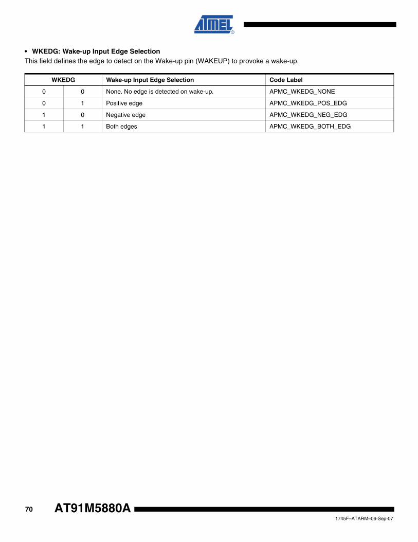
• WKEDG: Wake-up Input Edge SelectionThis field defines the edge to detect on the Wake-up pin (WAKEUP) to provoke a wake-up.
WKEDG Wake-up Input Edge Selection Code Label
0 0 None. No edge is detected on wake-up. APMC_WKEDG_NONE
0 1 Positive edge APMC_WKEDG_POS_EDG
1 0 Negative edge APMC_WKEDG_NEG_EDG
1 1 Both edges APMC_WKEDG_BOTH_EDG
701745F–ATARM–06-Sep-07
AT91M5880A

AT91M5880A
12.9.10 APMC Status Register Register Name: APMC_SR
Access Type: Read-only
Offset: 0x30
• MOSCS: Main Oscillator Status (Code Label APMC_MOSCS)0 = Main Oscillator output signal is not stabilized or the Main Oscillator is disabled.
1 = The Main Oscillator is enabled and its output is stabilized. Actually, this bit indicates that the Main Oscillator counterreached 0.
• LOCK: PLL Lock Status (Code Label APMC_PLL_LOCK)0 = PLL output signal or main oscillator output signal is not stabilized, or the main oscillator is disabled.
1 = Main Oscillator is enabled and its output is stabilized and the PLL output signal is stabilized. Actually, this bit is setwhen the PLL Lock Counter reaches 0.
31 30 29 28 27 26 25 24
– – – – – – – –
23 22 21 20 19 18 17 16
– – – – – – – –
15 14 13 12 11 10 9 8
– – – – – – – –
7 6 5 4 3 2 1 0
– – – – – – LOCK MOSCS
711745F–ATARM–06-Sep-07

12.9.11 APMC Interrupt Enable Register Register Name: APMC_IER
Access Type: Write-only
Offset: 0x34
• MOSCS: Main Oscillator Interrupt Enable (Code Label APMC_MOSCS)0 = No effect.
1 = Enables the Main Oscillator Stabilized Interrupt.
• LOCK: PLL Lock Interrupt Enable (Code Label APMC_PLL_LOCK)0 = No effect.
1 = Enables the PLL Lock Interrupt.
12.9.12 APMC Interrupt Disable Register Register Name: APMC_IDR
Access Type: Write-only
Offset: 0x38
• MOSCS: Main Oscillator Interrupt Disable (Code Label APMC_MOSCS)0 = No effect.
1 = Disables the Main Oscillator Stabilized Interrupt.
• LOCK: PLL Lock Interrupt Disable (Code Label APMC_PLL_LOCK)0 = No effect.
1 = Disables the PLL Lock Interrupt.
31 30 29 28 27 26 25 24
– – – – – – – –
23 22 21 20 19 18 17 16
– – – – – – – –
15 14 13 12 11 10 9 8
– – – – – – – –
7 6 5 4 3 2 1 0
– – – – – – LOCK MOSCS
31 30 29 28 27 26 25 24
– – – – – – – –
23 22 21 20 19 18 17 16
– – – – – – – –
15 14 13 12 11 10 9 8
– – – – – – – –
7 6 5 4 3 2 1 0
– – – – – – LOCK MOSCS
721745F–ATARM–06-Sep-07
AT91M5880A

AT91M5880A
12.9.13 APMC Interrupt Mask Register Register Name: APMC_IMR
Access Type: Read-only
Reset Value: 0x0
Offset: 0x3C
• MOSCS: Main Oscillator Interrupt Mask (Code Label APMC_MOSCS)0 = The Main Oscillator Interrupt is disabled.
1 = The Main Oscillator Interrupt is enabled.
• LOCK: PLL Lock Interrupt Mask (Code Label APMC_PLL_LOCK)0 = The PLL Lock Interrupt is disabled.
1 = The PLL Lock Interrupt is enabled.
31 30 29 28 27 26 25 24
– – – – – – – –
23 22 21 20 19 18 17 16
– – – – – – – –
15 14 13 12 11 10 9 8
– – – – – – – –
7 6 5 4 3 2 1 0
– – – – – – LOCK MOSCS
731745F–ATARM–06-Sep-07

13. RTC: Real-time ClockThe AT91M55800A features a Real-time Clock (RTC) peripheral that is designed for very lowpower consumption. It combines a complete time-of-day clock with alarm and a two-hundredyear Gregorian calendar, complemented by a programmable periodic interrupt.
The time and calendar values are coded in Binary-Coded Decimal (BCD) format. The time for-mat can be 24-hour mode or 12-hour mode with an AM/PM indicator.
Updating time and calendar fields and configuring the alarm fields is performed by a parallel cap-ture on the 32-bit data bus. An entry control is performed to avoid loading registers withincompatible BCD format data or with an incompatible date according to the current month/year/century.
13.1 Year 2000 ConformityThe Real-time Clock complies fully with the Year 2000 Conformity Requirements as stated in theBritish Standards Institution Document Ref BSI-DISC PD2000-1: “Year 2000 conformity shallmean that neither performance nor functionality is affected by dates prior to, during and after theyear 2000”.
It has been tested to be compliant with the four associated rules:
1. No value for current date will cause any interruption in operation.
2. Date-based functionality must behave consistently for dates prior to, during and after year 2000.
3. In all interfaces and data storage, the century in any date must be specified either explicitly or by unambiguous algorithms or inferencing rules.
4. Year 2000 must be recognized as a leap year.
The RTC represents the year as a four-digit number (1998, 1999, 2000, 2001, etc.) so that thecentury is unambiguously identified, in accordance with Rule 3.
Figure 13-1. RTC Block Diagram
Bus Interface
32768 Divider TimeSLCK:Slow Clock
AdvancedPeripheral
Bus
AIC
DateRTCIRQ
Entry Control
Interrupt Control
741745F–ATARM–06-Sep-07
AT91M5880A

AT91M5880A
13.2 Functional DescriptionThe RTC provides a full Binary-Coded Decimal (BCD) clock which includes century (19/20), year(with leap years), month, date, day, hours, minutes and seconds.
The valid year range is 1900 to 2099, a two-hundred year Gregorian calendar achieving full Y2Kcompliance.
The RTC can operate in 24-hour mode or in 12-hour mode with an AM/PM indicator.
Corrections for leap years are included (all years divisible by 4 being leap years, including year2000). This is correct up to the year 2099.
13.2.1 TimingThe RTC is updated in real-time at one second intervals in normal mode for the counters of sec-onds, at 1 minute intervals for the counter of minutes and so on.
Due to the asynchronous operation of the RTC with respect to the rest of the chip, to be certainthat the value read in the RTC registers (century, year, month, date, day, hours, minutes, sec-onds) are valid and stable, it is necessary to read these registers twice. If the data is the sameboth times, then it is valid. Therefore, a minimum of two and a maximum of three accesses isrequired.
13.2.2 AlarmThe RTC has five programmable fields with which to program an alarm: MONTH and DATE inthe Calendar Alarm Register (RTC_CAR), and SEC, MIN and HOUR in the Time Alarm Register(RTC_TAR). Each of these fields can be enabled or disabled using the bits MTHEN, DATEN,SECEN, MINEN, HOUREN to match the alarm condition.
• If all the fields are enabled, an alarm flag is generated (the corresponding flag is asserted and an interrupt generated if enabled) at a given month, date, hour, minute and second.
• If only the “seconds” field is enabled, then an alarm is generated every minute.
• Depending on the combination of fields enabled, a large number of possibilities are available to the user ranging from minutes to 365/366 days.
13.2.3 Error CheckingA verification on user interface data is performed when accessing the century, year, month,date, day, hours, minutes, seconds and alarms. A check is performed on illegal BCD entriessuch as illegal date of the month with regards to the year and century configured.
If one of the time fields is not correct, the data is not loaded into the register/counter and a flag isset in the Valid Entry Register (RTC_VER). This flag cannot be reset by the user. It is reset assoon as an acceptable value is programmed. This avoids any further side effects in the hard-ware. The same processing is done for the alarm.
The following checks are processed:
1. Century (check if it is in range 19 - 20)
2. Year (BCD entry check)
3. Date (check range 01 - 31)
4. Month (check if it is in BCD range 01 - 12, check validity regarding “date”)
5. Day (check range 1 - 7)
751745F–ATARM–06-Sep-07

6. Hour (BCD check, in 24-hour mode check range 00 - 23 and check that AM/PM flag is not set if RTC is set in 24-Hour mode, in 12-Hour mode check range 01 - 12)
7. Minute (check BCD and range 00 - 59)
8. Second (check BCD and range 00 - 59)Note: If the 12-hour mode is selected by means of the RTC_MODE register, a 12-hour value can be pro-
grammed and the returned value on RTC_TIME will be the corresponding 24-hour value. The entry control checks the value of the AM/PM indicator (bit 22 of RTC_TIME register) to determine the range to be checked.
13.2.4 Updating Time/CalendarTo update any of the time/calendar fields, the user must first stop the RTC by setting the corre-sponding field in the Mode Register (RTC_MR). Bit UPDTIM must be set to update time fields(hour, minute, second) and bit UPDCAL must be set to update calendar fields (century, year,month, date, day).
Then the user must poll or wait for the interrupt (if enabled) of bit ACKUPD in the Status Register(RTC_SR). Once the bit reads 1 (the user must clear this status bit by writing ACKUPD to 1 inRTC_SCR), the user can write to the appropriate register.
Once the update is finished, the user must reset (0) UPDTIM and/or UPDCAL in the Mode Reg-ister (RTC_MR).
When programming the calendar fields, the time fields remain enabled. This avoids a time slip incase the user stays in the calendar update phase for several tens of seconds or more.
761745F–ATARM–06-Sep-07
AT91M5880A

AT91M5880A
13.3 RTC User Interface Base Address:0xFFFB8000 (Code Label RTC_BASE)
Table 13-1. Register Mapping
Offset Register Name Access Reset State
0x0000 Mode Register RTC_MR Read/Write 0x00000000
0x0004 Hour Mode Register RTC_HMR Read/Write 0x00000000
0x0008 Time Register RTC_TIMR Read/Write 0x00000000
0x000C Calendar Register RTC_CALR Read/Write 0x01819819
0x0010 Time Alarm Register RTC_TAR Read/Write 0x00000000
0x0014 Calendar Alarm Register RTC_CAR Read/Write 0x00000000
0x0018 Status Register RTC_SR Read-only 0x00000000
0x001C Status Clear Register RTC_SCR Write-only –
0x0020 Interrupt Enable Register RTC_IER Write-only –
0x0024 Interrupt Disable Register RTC_IDR Write-only –
0x0028 Interrupt Mask Register RTC_IMR Read-only 0x00000000
0x002C Valid Entry Register RTC_VER Read-only 0x00000000
771745F–ATARM–06-Sep-07

13.3.1 RTC Mode RegisterRegister Name: RTC_MR
Access: Read/Write
Offset: 0x00
• UPDTIM: Update Request Time Register (Code Label RTC_UPDTIM)0 = Enables the RTC time counting.
1 = Stops the RTC time counting.
Time counting consists of second, minute and hour counters. Time counters can be programmed once this bit is set.
• UPDCAL: Update Request Calendar Register (Code Label RTC_UPDCAL)0 = Disables the RTC calendar counting.
1 = Stops the RTC calendar counting.
Calendar counting consists of day, date, month, year and century counters. Calendar counters can be programmed oncethis bit is set.
• TEVSEL: Time Event SelectionThe event which generates the flag TIMEV in RTC_SR (Status Register) depends on the value of TEVSEL.
• CEVSEL: Calendar Event SelectionThe event which generates the flag CALEV in RTC_SR depends on the value of CEVSEL.
31 30 29 28 27 26 25 24
– – – – – – – –
23 22 21 20 19 18 17 16
– – – – – – CEVSEL
15 14 13 12 11 10 9 8
– – – – – – TEVSEL
7 6 5 4 3 2 1 0
– – – – – – UPDCAL UPDTIM
TEVSEL Event Code Label
0 0 Minute change RTC_TEVSEL_MN_CHG
0 1 Hour change RTC_TEVSEL_HR_CHG
1 0 Every day at midnight RTC_TEVSEL_EVDAY_MD
1 1 Every day at noon RTC_TEVSEL_EVDAY_NOON
CEVSEL Event Code Label
0 0 Week change (every Monday at time 00:00:00) RTC_CEVSEL_WEEK_CHG
0 1 Month change (every 01 of each month at time 00:00:00) RTC_CEVSEL_MONTH_CHG
1 0 Year change (every January 1st at time 00:00:00) RTC_CEVSEL_YEAR_CHG
1 1 Reserved –
781745F–ATARM–06-Sep-07
AT91M5880A
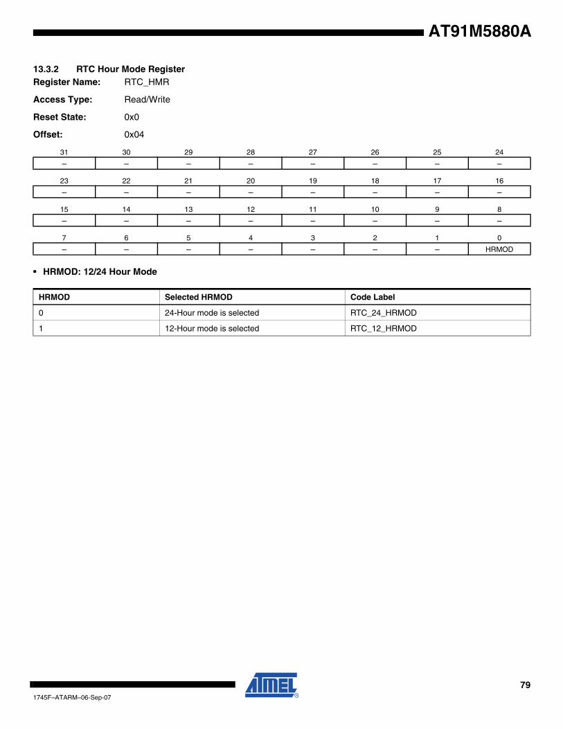
AT91M5880A
13.3.2 RTC Hour Mode RegisterRegister Name: RTC_HMR
Access Type: Read/Write
Reset State: 0x0
Offset: 0x04
• HRMOD: 12/24 Hour Mode
31 30 29 28 27 26 25 24
– – – – – – – –
23 22 21 20 19 18 17 16
– – – – – – – –
15 14 13 12 11 10 9 8
– – – – – – – –
7 6 5 4 3 2 1 0
– – – – – – – HRMOD
HRMOD Selected HRMOD Code Label
0 24-Hour mode is selected RTC_24_HRMOD
1 12-Hour mode is selected RTC_12_HRMOD
791745F–ATARM–06-Sep-07
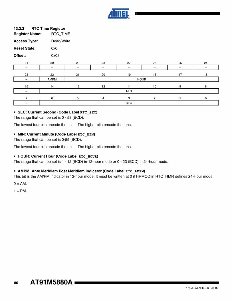
13.3.3 RTC Time RegisterRegister Name: RTC_TIMR
Access Type: Read/Write
Reset State: 0x0
Offset: 0x08
• SEC: Current Second (Code Label RTC_SEC)The range that can be set is 0 - 59 (BCD).
The lowest four bits encode the units. The higher bits encode the tens.
• MIN: Current Minute (Code Label RTC_MIN)The range that can be set is 0-59 (BCD).
The lowest four bits encode the units. The higher bits encode the tens.
• HOUR: Current Hour (Code Label RTC_HOUR)The range that can be set is 1 - 12 (BCD) in 12-hour mode or 0 - 23 (BCD) in 24-hour mode.
• AMPM: Ante Meridiem Post Meridiem Indicator (Code Label RTC_AMPM)This bit is the AM/PM indicator in 12-hour mode. It must be written at 0 if HRMOD in RTC_HMR defines 24-Hour mode.
0 = AM.
1 = PM.
31 30 29 28 27 26 25 24
– – – – – – – –
23 22 21 20 19 18 17 16
– AMPM HOUR
15 14 13 12 11 10 9 8
– MIN
7 6 5 4 3 2 1 0
– SEC
801745F–ATARM–06-Sep-07
AT91M5880A

AT91M5880A
13.3.4 RTC Calendar RegisterRegister Name: RTC_CALR
Access Type: Read/Write
Reset State: 0x01819819
Offset: 0x0C
• CENT: Current Century (Code Label RTC_CENT)The range that can be set is 19 - 20 (BCD).
The lowest four bits encode the units. The higher bits encode the tens.
• YEAR: Current Year (Code Label RTC_YEAR)The range that can be set is 00 - 99 (BCD).
The lowest four bits encode the units. The higher bits encode the tens.
• MONTH: Current Month (Code Label RTC_MONTH)The range that can be set is 01 - 12 (BCD).
The lowest four bits encode the units. The higher bits encode the tens.
• DAY: Current Day (Code Label RTC_DAY)The range that can be set is 1 - 7 (BCD).
The significance of the number (which number represents which day) is user defined as it has no effect on the datecounter.
• DATE: Current Date (Code Label RTC_DATE)The range that can be set is 01 - 31 (BCD).
The lowest four bits encode the units. The higher bits encode the tens.
31 30 29 28 27 26 25 24
– – DATE
23 22 21 20 19 18 17 16
DAY MONTH
15 14 13 12 11 10 9 8
YEAR
7 6 5 4 3 2 1 0
– – CENT
811745F–ATARM–06-Sep-07

13.3.5 RTC Time Alarm RegisterRegister Name: RTC_TAR
Access Type: Read/Write
Reset State: 0x0
Offset: 0x10
• SEC: Second AlarmThis field is the alarm field corresponding to the BCD-coded second counter.
• SECEN: Second Alarm Enable
• MIN: Minute AlarmThis field is the alarm field corresponding to the BCD-coded minute counter.
• MINEN: Minute Alarm Enable
• HOUR: Hour AlarmThis field is the alarm field corresponding to the BCD-coded hour counter.
• AMPM: AM/PM IndicatorThis bit is the AM/PM indicator in 12-Hour mode. It must be written at 0 if HRMOD in RTC_HMR defines 24-Hour mode.
• HOUREN: Hour Alarm Enable
31 30 29 28 27 26 25 24
– – – – – – – –
23 22 21 20 19 18 17 16
HOUREN AMPM HOUR
15 14 13 12 11 10 9 8
MINEN MIN
7 6 5 4 3 2 1 0
SECEN SEC
SECEN Selected SECEN Code Label
0 The second matching alarm is disabled. RTC_SEC_ALARM_DIS
1 The second matching alarm is enabled. RTC_SEC_ALARM_EN
MINEN Selected MINEN Code Label
0 The minute matching alarm is disabled. RTC_MIN_ALARM_DIS
1 The minute matching alarm is enabled. RTC_MIN_ALARM_EN
HOUREN Selected HOUREN Code Label
0 The hour matching alarm is disabled. RTC_HOUR_ALARM_DIS
1 The hour matching alarm is enabled. RTC_HOUR_ALARM_EN
821745F–ATARM–06-Sep-07
AT91M5880A

AT91M5880A
13.3.6 RTC Calendar Alarm RegisterRegister Name: RTC_CAR
Access Type: Read/Write
Reset State: 0x0
Offset: 0x14
• MONTH: Month AlarmThis field is the alarm field corresponding to the BCD-coded month counter.
• MTHEN: Month Alarm Enable
• DATE: Date AlarmThis field is the alarm field corresponding to the BCD-coded date counter.
• DATEN: Date Alarm Enable
31 30 29 28 27 26 25 24
DATEN – DATE
23 22 21 20 19 18 17 16
MTHEN – – MONTH
15 14 13 12 11 10 9 8
– – – – – – – –
7 6 5 4 3 2 1 0
– – – – – – – –
MTHEN Selected MTHEN Code Label
0 The month matching alarm is disabled. RTC_MONTH_ALARM_DIS
1 The month matching alarm is enabled. RTC_MONTH_ALARM_EN
DATEN Selected DATEN Code Label
0 The date matching alarm is disabled. RTC_DATE_ALARM_DIS
1 The date matching alarm is enabled. RTC_DATE_ALARM_EN
831745F–ATARM–06-Sep-07
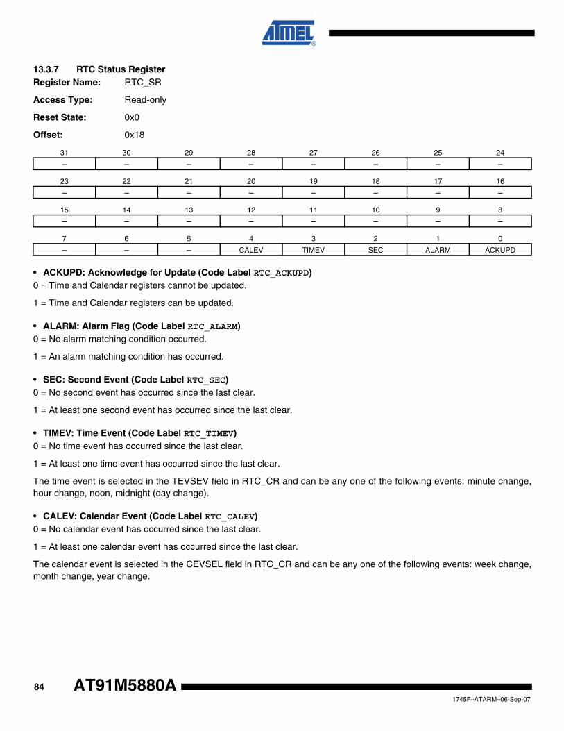
13.3.7 RTC Status RegisterRegister Name: RTC_SR
Access Type: Read-only
Reset State: 0x0
Offset: 0x18
• ACKUPD: Acknowledge for Update (Code Label RTC_ACKUPD)0 = Time and Calendar registers cannot be updated.
1 = Time and Calendar registers can be updated.
• ALARM: Alarm Flag (Code Label RTC_ALARM)0 = No alarm matching condition occurred.
1 = An alarm matching condition has occurred.
• SEC: Second Event (Code Label RTC_SEC)0 = No second event has occurred since the last clear.
1 = At least one second event has occurred since the last clear.
• TIMEV: Time Event (Code Label RTC_TIMEV)0 = No time event has occurred since the last clear.
1 = At least one time event has occurred since the last clear.
The time event is selected in the TEVSEV field in RTC_CR and can be any one of the following events: minute change,hour change, noon, midnight (day change).
• CALEV: Calendar Event (Code Label RTC_CALEV)0 = No calendar event has occurred since the last clear.
1 = At least one calendar event has occurred since the last clear.
The calendar event is selected in the CEVSEL field in RTC_CR and can be any one of the following events: week change,month change, year change.
31 30 29 28 27 26 25 24
– – – – – – – –
23 22 21 20 19 18 17 16
– – – – – – – –
15 14 13 12 11 10 9 8
– – – – – – – –
7 6 5 4 3 2 1 0
– – – CALEV TIMEV SEC ALARM ACKUPD
841745F–ATARM–06-Sep-07
AT91M5880A

AT91M5880A
13.3.8 RTC Status Clear RegisterRegister Name: RTC_SCR
Access Type: Write-only
Offset: 0x1C
• ACKUPD: Acknowledge for Update Interrupt Clear (Code Label RTC_ACKUPD)0 = No effect.
1 = Clears Acknowledge for Update status bit.
• ALARM: Alarm Flag Interrupt Clear (Code Label RTC_ALARM)0 = No effect.
1 = Clears Alarm Flag bit.
• SEC: Second Event Interrupt Clear (Code Label RTC_SEC)0 = No effect.
1 = Clears Second Event bit.
• TIMEV: Time Event Interrupt Clear (Code Label RTC_TIMEV)0 = No effect.
1 = Clears Time Event bit.
• CALEV: Calendar Event Interrupt Clear (Code Label RTC_CALEV)0 = No effect.
1 = Clears Calendar Event bit.
31 30 29 28 27 26 25 24
– – – – – – – –
23 22 21 20 19 18 17 16
– – – – – – – –
15 14 13 12 11 10 9 8
– – – – – – – –
7 6 5 4 3 2 1 0
– – – CALEV TIMEV SEC ALARM ACKUPD
851745F–ATARM–06-Sep-07

13.3.9 RTC Interrupt Enable RegisterRegister Name: RTC_IER
Access Type: Write-only
Offset: 0x20
• ACKUPD: Acknowledge Update Interrupt Enable (Code Label RTC_ACKUPD)0 = No effect.
1 = The acknowledge for update interrupt is enabled.
• ALARM: Alarm Interrupt Enable (Code Label RTC_ALARM)0 = No effect.
1 = The alarm interrupt is enabled.
• SEC: Second Event Interrupt Enable (Code Label RTC_SEC)0 = No effect.
1 = The second periodic interrupt is enabled.
• TIMEV: Time Event Interrupt Enable (Code Label RTC_TIMEV)0 = No effect.
1 = The selected time event interrupt is enabled.
• CALEV: Calendar Event Interrupt Enable (Code Label RTC_CALEV)0 = No effect.
1 = The selected calendar event interrupt is enabled.
31 30 29 28 27 26 25 24
– – – – – – – –
23 22 21 20 19 18 17 16
– – – – – – – –
15 14 13 12 11 10 9 8
– – – – – – – –
7 6 5 4 3 2 1 0
– – – CALEV TIMEV SEC ALARM ACKUPD
861745F–ATARM–06-Sep-07
AT91M5880A

AT91M5880A
13.3.10 RTC Interrupt Disable RegisterRegister Name: RTC_IDR
Access Type: Write-only
Offset: 0x24
• ACKUPD: Acknowledge Update Interrupt Disable (Code Label RTC_ACKUPD)0 = No effect.
1 = The acknowledge for update interrupt is disabled.
• ALARM: Alarm Interrupt Disable (Code Label RTC_ALARM)0 = No effect.
1 = The alarm interrupt is disabled.
• SEC: Second Event Interrupt Disable (Code Label RTC_SEC)0 = No effect.
1 = The second periodic interrupt is disabled.
• TIMEV: Time Event Interrupt Disable (Code Label RTC_TIMEV)0 = No effect.
1 = The selected time event interrupt is disabled.
• CALEV: Calendar Event Interrupt Disable (Code Label RTC_CALEV)0 = No effect.
1 = The selected calendar event interrupt is disabled.
31 30 29 28 27 26 25 24
– – – – – – – –
23 22 21 20 19 18 17 16
– – – – – – – –
15 14 13 12 11 10 9 8
– – – – – – – –
7 6 5 4 3 2 1 0
– – – CALEV TIMEV SEC ALARM ACKUPD
871745F–ATARM–06-Sep-07

13.3.11 RTC Interrupt Mask RegisterRegister Name: RTC_IMR
Access Type: Read-only
Reset State: 0x0
Offset: 0x28
• ACKUPD: Acknowledge Update Interrupt Mask (Code Label RTC_ACKUPD)0 = The acknowledge for update interrupt is disabled.
1 = The acknowledge for update interrupt is enabled.
• ALARM: Alarm Interrupt Mask (Code Label RTC_ALARM)0 = The alarm interrupt is disabled.
1 = The alarm interrupt is enabled.
• SEC: Second Event Interrupt Mask (Code Label RTC_SEC)0 = The second periodic interrupt is disabled.
1 = The second periodic interrupt is enabled.
• TIMEV: Time Event Interrupt Mask (Code Label RTC_TIMEV)0 = The selected time event interrupt is disabled.
1 = The selected time event interrupt is enabled.
• CALEV: Calendar Event Interrupt Mask (Code Label RTC_CALEV)0 = The selected calendar event interrupt is disabled.
1 = The selected calendar event interrupt is enabled.
31 30 29 28 27 26 25 24
– – – – – – – –
23 22 21 20 19 18 17 16
– – – – – – – –
15 14 13 12 11 10 9 8
– – – – – – – –
7 6 5 4 3 2 1 0
– – – CALEV TIMEV SEC ALARM ACKUPD
881745F–ATARM–06-Sep-07
AT91M5880A

AT91M5880A
13.3.12 RTC Valid Entry RegisterRegister Name: RTC_VER
Access Type: Read-only
Reset State: 0x0
Offset: 0x2C
• NVT: Non-Valid Time (Code Label RTC_NVT)0 = No invalid data has been detected in RTC_TIMR.
1 = RTC_TIMR has contained invalid data since it was last programmed.
• NVC: Non-Valid Calendar (Code Label RTC_NVC)0 = No invalid data has been detected in RTC_CALR.
1 = RTC_CALR has contained invalid data since it was last programmed.
• NVTAL: Non-Valid Time Alarm (Code Label RTC_NVTAL)0 = No invalid data has been detected in RTC_TAR.
1 = RTC_TAR has contained invalid data since it was last programmed.
• NVCAL: Non-Valid Calendar Alarm (Code Label RTC_NVCAL)0 = No invalid data has been detected in RTC_CAR.
1 = RTC_CAR has contained invalid data since it was last programmed.
31 30 29 28 27 26 25 24
– – – – – – – –
23 22 21 20 19 18 17 16
– – – – – – – –
15 14 13 12 11 10 9 8
– – – – – – – –
7 6 5 4 3 2 1 0
– – – – NVCAL NVTAL NVC NVT
891745F–ATARM–06-Sep-07

14. WD: Watchdog TimerThe AT91M55800A has an internal Watchdog Timer that can be used to prevent system lock-upif the software becomes trapped in a deadlock.
In normal operation the user reloads the watchdog at regular intervals before the timer overflowoccurs. If an overflow does occur, the watchdog timer generates one or a combination of the fol-lowing signals, depending on the parameters in WD_OMR (Overflow Mode Register):
• If RSTEN is set, an internal reset is generated (WD_RESET as shown in Figure 14-1).
• If IRQEN is set, a pulse is generated on the signal WDIRQ which is connected to the Advanced Interrupt Controller
• If EXTEN is set, a low level is driven on the NWDOVF signal for a duration of 8 MCK cycles.
The watchdog timer has a 16-bit down counter. Bits 12 - 15 of the value loaded when the watch-dog is restarted are programmable using the HPVC parameter in WD_CMR (Clock Mode). Fourclock sources are available to the watchdog counter: MCK/32, MCK/128, MCK/1024 orMCK/4096. The selection is made using the WDCLKS parameter in WD_CMR. This provides aprogrammable time-out period of 4 ms to 8 sec. with a 33 MHz system clock.
All write accesses are protected by control access keys to help prevent corruption of the watch-dog should an error condition occur. To update the contents of the mode and control registers itis necessary to write the correct bit pattern to the control access key bits at the same time as thecontrol bits are written (the same write access).
Figure 14-1. Watchdog Timer Block Diagram
Advanced PeripheralBus (APB)
WD_RESET
WDIRQ
MCK/32
MCK/128
MCK/1024
MCK/4096
Control Logic
Clock Select16-Bit
ProgrammableDown CounterCLK_CNT
Clear
Overflow
NWDOVF
901745F–ATARM–06-Sep-07
AT91M5880A

AT91M5880A
14.1 WD User InterfaceWD Base Address: 0xFFFF8000 (Code Label WD_BASE)
Table 14-1. Register Mapping
Offset Register Name Access Reset
0x00 Overflow Mode Register WD_OMR Read/Write 0
0x04 Clock Mode Register WD_CMR Read/Write 0
0x08 Control Register WD_CR Write-only –
0x0C Status Register WD_SR Read-only 0
911745F–ATARM–06-Sep-07

14.1.1 WD Overflow Mode RegisterName: WD_OMR
Access: Read/Write
Reset Value: 0
Offset: 0x00
• WDEN: Watchdog Enable (Code Label WD_WDEN)0 = Watchdog is disabled and does not generate any signals.
1 = Watchdog is enabled and generates enabled signals.
• RSTEN: Reset Enable (Code Label WD_RSTEN)0 = Generation of an internal reset by the Watchdog is disabled.
1 = When overflow occurs, the Watchdog generates an internal reset.
• IRQEN: Interrupt Enable (Code Label WD_IRQEN)0 = Generation of an interrupt by the Watchdog is disabled.
1 = When overflow occurs, the Watchdog generates an interrupt.
• EXTEN: External Signal Enable (Code Label WD_EXTEN)0 = Generation of a pulse on the pin NWDOVF by the Watchdog is disabled.
1 = When an overflow occurs, a pulse on the pin NWDOVF is generated.
• OKEY: Overflow Access Key (Code Label WD_OKEY)Used only when writing WD_OMR. OKEY is read as 0.
0x234 = Write access in WD_OMR is allowed.
Other value = Write access in WD_OMR is prohibited.
31 30 29 28 27 26 25 24
– – – – – – – –
23 22 21 20 19 18 17 16
– – – – – – – –
15 14 13 12 11 10 9 8
OKEY
7 6 5 4 3 2 1 0
OKEY EXTEN IRQEN RSTEN WDEN
921745F–ATARM–06-Sep-07
AT91M5880A

AT91M5880A
14.1.2 WD Clock Mode RegisterName: WD_CMR
Access: Read/Write
Reset Value: 0
Offset: 0x04
• WDCLKS: Clock Selection
• HPCV: High Pre-load Counter Value (Code Label WD_HPCV)Counter is preloaded when watchdog counter is restarted with bits 0 to 11 set (FFF) and bits 12 to 15 equaling HPCV.
• CKEY: Clock Access Key (Code Label WD_CKEY)Used only when writing WD_CMR. CKEY is read as 0.
0x06E: Write access in WD_CMR is allowed.
Other value: Write access in WD_CMR is prohibited.
31 30 29 28 27 26 25 24
– – – – – – – –
23 22 21 20 19 18 17 16
– – – – – – – –
15 14 13 12 11 10 9 8
CKEY
7 6 5 4 3 2 1 0
CKEY – HPCV WDCLKS
WDCLKS Clock Selected
Code Label
WD_WDCLKS
0 0 MCK/32 WD_WDCLKS_MCK32
0 1 MCK/128 WD_WDCLKS_MCK128
1 0 MCK/1024 WD_WDCLKS_MCK1024
1 1 MCK/4096 WD_WDCLKS_MCK4096
931745F–ATARM–06-Sep-07

14.1.3 WD Control RegisterName: WD_CR
Access: Write-only
Offset: 0x08
• RSTKEY: Restart Key (Code Label WD_RSTKEY)0xC071 = Watch Dog counter is restarted.
Other value = No effect.
31 30 29 28 27 26 25 24
– – – – – – – –
23 22 21 20 19 18 17 16
– – – – – – – –
15 14 13 12 11 10 9 8
RSTKEY
7 6 5 4 3 2 1 0
RSTKEY
941745F–ATARM–06-Sep-07
AT91M5880A

AT91M5880A
14.1.4 WD Status RegisterName: WD_SR
Access: Read-only
Reset Value: 0x0
Offset: 0x0C
• WDOVF: Watchdog Overflow (Code Label WD_WDOVF)0 = No watchdog overflow.
1 = A watchdog overflow has occurred since the last restart of the watchdog counter or since internal or external reset.
14.1.5 WD Enabling SequenceTo enable the Watchdog Timer, the sequence is as follows:
1. Disable the Watchdog by clearing the bit WDEN:Write 0x2340 to WD_OMRThis step is unnecessary if the WD is already disabled (reset state).
2. Initialize the WD Clock Mode Register:
3. Write 0x373C to WD_CMR(HPCV = 15 and WDCLKS = MCK/8)
4. Restart the timer: Write 0xC071 to WD_CR
5. Enable the watchdog:Write 0x2345 to WD_OMR (interrupt enabled)
31 30 29 28 27 26 25 24
– – – – – – – –
23 22 21 20 19 18 17 16
– – – – – – – –
15 14 13 12 11 10 9 8
– – – – – – – –
7 6 5 4 3 2 1 0
– – – – – – – WDOVF
951745F–ATARM–06-Sep-07

15. AIC: Advanced Interrupt Controller The AT91M55800A has an 8-level priority, individually maskable, vectored interrupt controller.This feature substantially reduces the software and real-time overhead in handling internal andexternal interrupts.
The interrupt controller is connected to the NFIQ (fast interrupt request) and the NIRQ (standardinterrupt request) inputs of the ARM7TDMI processor. The processor’s NFIQ line can only beasserted by the external fast interrupt request input: FIQ. The NIRQ line can be asserted by theinterrupts generated by the on-chip peripherals and the external interrupt request lines: IRQ0 toIRQ5.
An 8-level priority encoder allows the customer to define the priority between the different NIRQinterrupt sources.
Internal sources are programmed to be level sensitive or edge-triggered. External sources canbe programmed to be positive or negative edge-triggered or high- or low-level sensitive.
The interrupt sources are listed in Table 15-1 on page 97 and the AIC programmable registers inTable 15-2 on page 102.
Figure 15-1. Advanced Interrupt Controller Block Diagram
Note: After a hardware reset, the AIC pins are controlled by the PIO Controller. They must be configured to be controlled by the peripheral before being used.
Control Logic
Memorization
Memorization PrioritizationController
NIRQManager
NFIQ Manager
FIQ Source
Advanced PeripheralBus (APB)
Internal Interrupt Sources
External Interrupt Sources
ARM7TDMICore
NFIQ
NIRQ
961745F–ATARM–06-Sep-07
AT91M5880A

AT91M5880A
Table 15-1. AIC Interrupt Sources
Interrupt Source Interrupt Name Interrupt Description
0 FIQ Fast interrupt
1 SWIRQ Software interrupt
2 US0IRQ USART Channel 0 interrupt
3 US1IRQ USART Channel 1 interrupt
4 US2IRQ USART Channel 2 interrupt
5 SPIRQ SPI interrupt
6 TC0IRQ Timer Channel 0 interrupt
7 TC1IRQ Timer Channel 1 interrupt
8 TC2IRQ Timer Channel 2 interrupt
9 TC3IRQ Timer Channel 3 interrupt
10 TC4IRQ Timer Channel 4 interrupt
11 TC5IRQ Timer Channel 5 interrupt
12 WDIRQ Watchdog interrupt
13 PIOAIRQ Parallel I/O Controller A interrupt
14 PIOBIRQ Parallel I/O Controller B interrupt
15 AD0IRQ Analog-to-digital Converter Channel 0 interrupt
16 AD1IRQ Analog-to-digital Converter Channel 1 interrupt
17 DA0IRQ Digital-to-analog Converter Channel 0 interrupt
18 DA1IRQ Digital-to-analog Converter Channel 1 interrupt
19 RTCIRQ Real-time Clock interrupt
20 APMCIRQ Advanced Power Management Controller interrupt
21 – Reserved
22 – Reserved
23 SLCKIRQ Slow Clock Interrupt
24 IRQ5 External interrupt 5
25 IRQ4 External interrupt 4
26 IRQ3 External interrupt 3
27 IRQ2 External interrupt 2
28 IRQ1 External interrupt 1
29 IRQ0 External interrupt 0
30 COMMRX RX Debug Communication Channel interrupt
31 COMMTX TX Debug Communication Channel interrupt
971745F–ATARM–06-Sep-07

15.1 Hardware Interrupt VectoringThe hardware interrupt vectoring reduces the number of instructions to reach the interrupt han-dler to only one. By storing the following instruction at address 0x00000018, the processor loadsthe program counter with the interrupt handler address stored in the AIC_IVR register. Executionis then vectored to the interrupt handler corresponding to the current interrupt.
ldr PC,[PC,# -&F20]
The current interrupt is the interrupt with the highest priority when the Interrupt Vector Register(AIC_IVR) is read. The value read in the AIC_IVR corresponds to the address stored in theSource Vector Register (AIC_SVR) of the current interrupt. Each interrupt source has its corre-sponding AIC_SVR. In order to take advantage of the hardware interrupt vectoring it isnecessary to store the address of each interrupt handler in the corresponding AIC_SVR, at sys-tem initialization.
15.2 Priority ControllerThe NIRQ line is controlled by an 8-level priority encoder. Each source has a programmable pri-ority level of 7 to 0. Level 7 is the highest priority and level 0 the lowest.
When the AIC receives more than one unmasked interrupt at a time, the interrupt with the high-est priority is serviced first. If both interrupts have equal priority, the interrupt with the lowestinterrupt source number (see Table Table 15-1) is serviced first.
The current priority level is defined as the priority level of the current interrupt at the time the reg-ister AIC_IVR is read (the interrupt which is serviced).
In the case when a higher priority unmasked interrupt occurs while an interrupt already exists,there are two possible outcomes depending on whether the AIC_IVR has been read.
• If the NIRQ line has been asserted but the AIC_IVR has not been read, then the processor reads the new higher priority interrupt handler address in the AIC_IVR register and the current interrupt level is updated.
• If the processor has already read the AIC_IVR then the NIRQ line is reasserted. When the processor has authorized nested interrupts to occur and reads the AIC_IVR again, it reads the new, higher priority interrupt handler address. At the same time the current priority value is pushed onto a first-in last-out stack and the current priority is updated to the higher priority.
When the end of interrupt command register (AIC_EOICR) is written the current interrupt level isupdated with the last stored interrupt level from the stack (if any). Hence at the end of a higherpriority interrupt, the AIC returns to the previous state corresponding to the preceding lower pri-ority interrupt which had been interrupted.
15.3 Interrupt HandlingThe interrupt handler must read the AIC_IVR as soon as possible. This de-asserts the NIRQrequest to the processor and clears the interrupt in case it is programmed to be edge-triggered.This permits the AIC to assert the NIRQ line again when a higher priority unmasked interruptoccurs.
At the end of the interrupt service routine, the end of interrupt command register (AIC_EOICR)must be written. This allows pending interrupts to be serviced.
981745F–ATARM–06-Sep-07
AT91M5880A

AT91M5880A
15.4 Interrupt MaskingEach interrupt source, including FIQ, can be enabled or disabled using the command registersAIC_IECR and AIC_IDCR. The interrupt mask can be read in the Read-only register AIC_IMR. Adisabled interrupt does not affect the servicing of other interrupts.
15.5 Interrupt Clearing and SettingAll interrupt sources which are programmed to be edge-triggered (including FIQ) can be individ-ually set or cleared by respectively writing to the registers AIC_ISCR and AIC_ICCR. Thisfunction of the interrupt controller is available for auto-test or software debug purposes.
15.6 Fast Interrupt RequestThe external FIQ line is the only source which can raise a fast interrupt request to the processor.Therefore, it has no priority controller.
The external FIQ line can be programmed to be positive or negative edge-triggered or high- orlow-level sensitive in the AIC_SMR0 register.
The fast interrupt handler address can be stored in the AIC_SVR0 register. The value writteninto this register is available by reading the AIC_FVR register when an FIQ interrupt is raised. Bystoring the following instruction at address 0x0000001C, the processor loads the programcounter with the interrupt handler address stored in the AIC_FVR register.
ldr PC,[PC,# -&F20]
Alternatively, the interrupt handler can be stored starting from address 0x0000001C asdescribed in the ARM7TDMI datasheet.
15.7 Software InterruptInterrupt source 1 of the advanced interrupt controller is a software interrupt. It must be pro-grammed to be edge-triggered in order to set or clear it by writing to the AIC_ISCR andAIC_ICCR.
This is totally independent of the SWI instruction of the ARM7TDMI processor.
15.8 Spurious InterruptWhen the AIC asserts the NIRQ line, the ARM7TDMI enters IRQ mode and the interrupt handlerreads the IVR. It may happen that the AIC de-asserts the NIRQ line after the core has taken intoaccount the NIRQ assertion and before the read of the IVR.
This behavior is called a Spurious Interrupt.
The AIC is able to detect these Spurious Interrupts and returns the Spurious Vector when theIVR is read. The Spurious Vector can be programmed by the user when the vector table isinitialized.
A Spurious Interrupt may occur in the following cases:
• With any sources programmed to be level sensitive, if the interrupt signal of the AIC input is de-asserted at the same time as it is taken into account by the ARM7TDMI.
• If an interrupt is asserted at the same time as the software is disabling the corresponding source through AIC_IDCR (this can happen due to the pipelining of the ARM Core).
991745F–ATARM–06-Sep-07

The same mechanism of Spurious Interrupt occurs if the ARM7TDMI reads the IVR (applicationsoftware or ICE) when there is no interrupt pending. This mechanism is also valid for the FIQinterrupts.
Once the AIC enters the Spurious Interrupt management, it asserts neither the NIRQ nor theNFIQ lines to the ARM7TDMI as long as the Spurious Interrupt is not acknowledged. Therefore,it is mandatory for the Spurious Interrupt Service Routine to acknowledge the “Spurious” behav-ior by writing to the AIC_EOICR (End of Interrupt) before returning to the interrupted software. Italso can perform other operation(s), e.g. trace possible undesirable behavior.
15.9 Protect ModeThe Protect Mode permits reading of the Interrupt Vector Register without performing the associ-ated automatic operations. This is necessary when working with a debug system.
When a Debug Monitor or an ICE reads the AIC User Interface, the IVR could be read. Thiswould have the following consequences in normal mode:
• If an enabled interrupt with a higher priority than the current one is pending, it would be stacked.
• If there is no enabled pending interrupt, the spurious vector would be returned.
In either case, an End of Interrupt Command would be necessary to acknowledge and to restorethe context of the AIC. This operation is generally not performed by the debug system. Hencethe debug system would become strongly intrusive, and could cause the application to enter anundesired state.
This is avoided by using Protect Mode.
The Protect Mode is enabled by setting the AIC bit in the SF Protect Mode Register.
When Protect Mode is enabled, the AIC performs interrupt stacking only when a write access isperformed on the AIC_IVR. Therefore, the Interrupt Service Routines must write (arbitrary data)to the AIC_IVR just after reading it.
The new context of the AIC, including the value of the Interrupt Status Register (AIC_ISR), isupdated with the current interrupt only when IVR is written.
An AIC_IVR read on its own (e.g. by a debugger), modifies neither the AIC context nor theAIC_ISR.
Extra AIC_IVR reads performed in between the read and the write can cause unpredictableresults. Therefore, it is strongly recommended not to set a breakpoint between these 2 actions,nor to stop the software.
The debug system must not write to the AIC_IVR as this would cause undesirable effects.
1001745F–ATARM–06-Sep-07
AT91M5880A

AT91M5880A
The following table shows the main steps of an interrupt and the order in which they are per-formed according to the mode:
Notes: 1. NIRQ de-assertion and automatic interrupt clearing if the source is programmed as level sensitive
2. Note that software which has been written and debugged using Protect Mode will run correctly in Normal Mode without modification. However in Normal Mode the AIC_IVR write has no effect and can be removed to optimize the code.
Action Normal Mode Protect Mode
Calculate active interrupt (higher than current or spurious)
Read AIC_IVR Read AIC_IVR
Determine and return the vector of the active interrupt
Read AIC_IVR Read AIC_IVR
Memorize interrupt Read AIC_IVR Read AIC_IVR
Push on internal stack the current priority level
Read AIC_IVR Write AIC_IVR
Acknowledge the interrupt (1) Read AIC_IVR Write AIC_IVR
No effect(2) Write AIC_IVR –
1011745F–ATARM–06-Sep-07

15.10 AIC User InterfaceBase Address: 0xFFFFF000 (Code Label AIC_BASE)
Note: 1. The reset value of this register depends on the level of the External IRQ lines. All other sources are cleared at reset.
Table 15-2. Register Mapping
Offset Register Name Access Reset
0x000 Source Mode Register 0 AIC_SMR0 Read/Write 0
0x004 Source Mode Register 1 AIC_SMR1 Read/Write 0
– – – Read/Write 0
0x07C Source Mode Register 31 AIC_SMR31 Read/Write 0
0x080 Source Vector Register 0 AIC_SVR0 Read/Write 0
0x084 Source Vector Register 1 AIC_SVR1 Read/Write 0
– – – Read/Write 0
0x0FC Source Vector Register 31 AIC_SVR31 Read/Write 0
0x100 IRQ Vector Register AIC_IVR Read-only 0
0x104 FIQ Vector Register AIC_FVR Read-only 0
0x108 Interrupt Status Register AIC_ISR Read-only 0
0x10C Interrupt Pending Register AIC_IPR Read-only see Note (1)
0x110 Interrupt Mask Register AIC_IMR Read-only 0
0x114 Core Interrupt Status Register AIC_CISR Read-only 0
0x118 Reserved – – –
0x11C Reserved – – –
0x120 Interrupt Enable Command Register AIC_IECR Write-only –
0x124 Interrupt Disable Command Register AIC_IDCR Write-only –
0x128 Interrupt Clear Command Register AIC_ICCR Write-only –
0x12C Interrupt Set Command Register AIC_ISCR Write-only –
0x130 End of Interrupt Command Register AIC_EOICR Write-only –
0x134 Spurious Vector Register AIC_SPU Read/Write 0
1021745F–ATARM–06-Sep-07
AT91M5880A

AT91M5880A
15.10.1 AIC Source Mode RegisterRegister Name: AIC_SMR0...AIC_SMR31
Access Type: Read/Write
Reset Value: 0
• PRIOR: Priority Level (Code Label AIC_PRIOR)Program the priority level for all sources except source 0 (FIQ).
The priority level can be between 0 (lowest) and 7 (highest).
The priority level is not used for the FIQ, in the SMR0.
• SRCTYPE: Interrupt Source Type (Code Label AIC_SRCTYPE)Program the input to be positive or negative edge-triggered or positive or negative level sensitive.
The active level or edge is not programmable for the internal sources.
31 30 29 28 27 26 25 24
– – – – – – – –
23 22 21 20 19 18 17 16
– – – – – – – –
15 14 13 12 11 10 9 8
– – – – – – – –
7 6 5 4 3 2 1 0
– SRCTYPE – – PRIOR
SRCTYPEInternal Sources Code Label Internal
External Sources Code Label External
0 0Level Sensitive
AIC_SRCTYPE_INT_LEVEL_SENSITIVELow-level Sensitive
AIC_SRCTYPE_EXT_LOW_LEVEL
0 1Edge-triggered
AIC_SRCTYPE_INT_EDGE_TRIGGEREDNegative Edge-triggered
AIC_SRCTYPE_EXT_NEGATIVE_EDGE
1 0Level Sensitive
AIC_SRCTYPE_INT_LEVEL_SENSITIVEHigh-level Sensitive
AIC_SRCTYPE_EXT_HIGH_LEVEL
1 1Edge-triggered
AIC_SRCTYPE_INT_EDGE_TRIGGEREDPositive Edge-triggered
AIC_SRCTYPE_EXT_POSITIVE_EDGE
1031745F–ATARM–06-Sep-07

15.10.2 AIC Source Vector RegisterRegister Name: AIC_SVR0..AIC_SVR31
Access Type: Read/Write
Reset Value: 0
• VECTOR: Interrupt Handler AddressThe user may store in these registers the addresses of the corresponding handler for each interrupt source.
15.10.3 AIC Interrupt Vector RegisterRegister Name: AIC_IVR
Access Type: Read-only
Reset Value: 0
Offset: 0x100
• IRQV: Interrupt Vector RegisterThe IRQ Vector Register contains the vector programmed by the user in the Source Vector Register corresponding to thecurrent interrupt.
The Source Vector Register (1 to 31) is indexed using the current interrupt number when the Interrupt Vector Register isread.
When there is no current interrupt, the IRQ Vector Register reads 0.
31 30 29 28 27 26 25 24
VECTOR
23 22 21 20 19 18 17 16
VECTOR
15 14 13 12 11 10 9 8
VECTOR
7 6 5 4 3 2 1 0
VECTOR
31 30 29 28 27 26 25 24
IRQV
23 22 21 20 19 18 17 16
IRQV
15 14 13 12 11 10 9 8
IRQV
7 6 5 4 3 2 1 0
IRQV
1041745F–ATARM–06-Sep-07
AT91M5880A

AT91M5880A
15.10.4 AIC FIQ Vector RegisterRegister Name: AIC_FVR
Access Type: Read-only
Reset Value: 0
Offset: 0x104
• FIQV: FIQ Vector RegisterThe FIQ Vector Register contains the vector programmed by the user in the Source Vector Register 0 which correspondsto FIQ.
15.10.5 AIC Interrupt Status RegisterRegister Name: AIC_ISR
Access Type: Read-only
Reset Value: 0
Offset: 0x108
• IRQID: Current IRQ Identifier (Code Label AIC_IRQID)The Interrupt Status Register returns the current interrupt source number.
31 30 29 28 27 26 25 24
FIQV
23 22 21 20 19 18 17 16
FIQV
15 14 13 12 11 10 9 8
FIQV
7 6 5 4 3 2 1 0
FIQV
31 30 29 28 27 26 25 24
– – – – – – – –
23 22 21 20 19 18 17 16
– – – – – – – –
15 14 13 12 11 10 9 8
– – – – – – – –
7 6 5 4 3 2 1 0
– – – IRQID
1051745F–ATARM–06-Sep-07
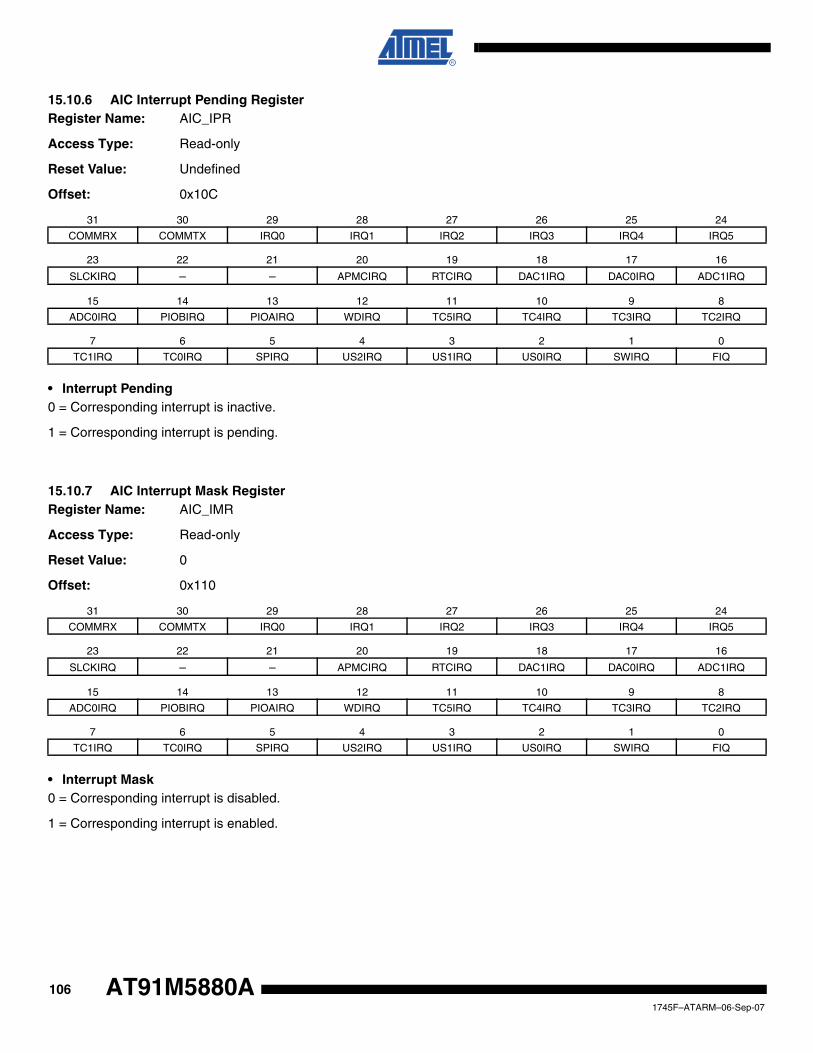
15.10.6 AIC Interrupt Pending RegisterRegister Name: AIC_IPR
Access Type: Read-only
Reset Value: Undefined
Offset: 0x10C
• Interrupt Pending0 = Corresponding interrupt is inactive.
1 = Corresponding interrupt is pending.
15.10.7 AIC Interrupt Mask RegisterRegister Name: AIC_IMR
Access Type: Read-only
Reset Value: 0
Offset: 0x110
• Interrupt Mask0 = Corresponding interrupt is disabled.
1 = Corresponding interrupt is enabled.
31 30 29 28 27 26 25 24
COMMRX COMMTX IRQ0 IRQ1 IRQ2 IRQ3 IRQ4 IRQ5
23 22 21 20 19 18 17 16
SLCKIRQ – – APMCIRQ RTCIRQ DAC1IRQ DAC0IRQ ADC1IRQ
15 14 13 12 11 10 9 8
ADC0IRQ PIOBIRQ PIOAIRQ WDIRQ TC5IRQ TC4IRQ TC3IRQ TC2IRQ
7 6 5 4 3 2 1 0
TC1IRQ TC0IRQ SPIRQ US2IRQ US1IRQ US0IRQ SWIRQ FIQ
31 30 29 28 27 26 25 24
COMMRX COMMTX IRQ0 IRQ1 IRQ2 IRQ3 IRQ4 IRQ5
23 22 21 20 19 18 17 16
SLCKIRQ – – APMCIRQ RTCIRQ DAC1IRQ DAC0IRQ ADC1IRQ
15 14 13 12 11 10 9 8
ADC0IRQ PIOBIRQ PIOAIRQ WDIRQ TC5IRQ TC4IRQ TC3IRQ TC2IRQ
7 6 5 4 3 2 1 0
TC1IRQ TC0IRQ SPIRQ US2IRQ US1IRQ US0IRQ SWIRQ FIQ
1061745F–ATARM–06-Sep-07
AT91M5880A

AT91M5880A
15.10.8 AIC Core Interrupt Status RegisterRegister Name: AIC_CISR
Access Type: Read-only
Reset Value: 0
Offset: 0x114
• NFIQ: NFIQ Status (Code Label AIC_NFIQ)0 = NFIQ line inactive.
1 = NFIQ line active.
• NIRQ: NIRQ Status (Code Label AIC_NIRQ)0 = NIRQ line inactive.
1 = NIRQ line active.
15.10.9 AIC Interrupt Enable Command RegisterRegister Name: AIC_IECR
Access Type: Write-only
Offset: 0x120
• Interrupt Enable0 = No effect.
1 = Enables corresponding interrupt.
31 30 29 28 27 26 25 24
– – – – – – – –
23 22 21 20 19 18 17 16
– – – – – – – –
15 14 13 12 11 10 9 8
– – – – – – – –
7 6 5 4 3 2 1 0
– – – – – – NIRQ NFIQ
31 30 29 28 27 26 25 24
COMMRX COMMTX IRQ0 IRQ1 IRQ2 IRQ3 IRQ4 IRQ5
23 22 21 20 19 18 17 16
SLCKIRQ – – APMCIRQ RTCIRQ DAC1IRQ DAC0IRQ ADC1IRQ
15 14 13 12 11 10 9 8
ADC0IRQ PIOBIRQ PIOAIRQ WDIRQ TC5IRQ TC4IRQ TC3IRQ TC2IRQ
7 6 5 4 3 2 1 0
TC1IRQ TC0IRQ SPIRQ US2IRQ US1IRQ US0IRQ SWIRQ FIQ
1071745F–ATARM–06-Sep-07

15.10.10 AIC Interrupt Disable Command RegisterRegister Name: AIC_IDCR
Access Type: Write-only
Offset: 0x124
• Interrupt Disable0 = No effect.
1 = Disables corresponding interrupt.
15.10.11 AIC Interrupt Clear Command RegisterRegister Name: AIC_ICCR
Access Type: Write-only
Offset: 0x128
• Interrupt Clear0 = No effect.
1 = Clears corresponding interrupt.
31 30 29 28 27 26 25 24
COMMRX COMMTX IRQ0 IRQ1 IRQ2 IRQ3 IRQ4 IRQ5
23 22 21 20 19 18 17 16
SLCKIRQ – – APMCIRQ RTCIRQ DAC1IRQ DAC0IRQ ADC1IRQ
15 14 13 12 11 10 9 8
ADC0IRQ PIOBIRQ PIOAIRQ WDIRQ TC5IRQ TC4IRQ TC3IRQ TC2IRQ
7 6 5 4 3 2 1 0
TC1IRQ TC0IRQ SPIRQ US2IRQ US1IRQ US0IRQ SWIRQ FIQ
31 30 29 28 27 26 25 24
COMMRX COMMTX IRQ0 IRQ1 IRQ2 IRQ3 IRQ4 IRQ5
23 22 21 20 19 18 17 16
SLCKIRQ – – APMCIRQ RTCIRQ DAC1IRQ DAC0IRQ ADC1IRQ
15 14 13 12 11 10 9 8
ADC0IRQ PIOBIRQ PIOAIRQ WDIRQ TC5IRQ TC4IRQ TC3IRQ TC2IRQ
7 6 5 4 3 2 1 0
TC1IRQ TC0IRQ SPIRQ US2IRQ US1IRQ US0IRQ SWIRQ FIQ
1081745F–ATARM–06-Sep-07
AT91M5880A

AT91M5880A
15.10.12 AIC Interrupt Set Command RegisterRegister Name: AIC_ISCR
Access Type: Write-only
Offset: 0x12C
• Interrupt Set0 = No effect.
1 = Sets corresponding interrupt.
15.10.13 AIC End of Interrupt Command RegisterRegister Name: AIC_EOICR
Access Type: Write-only
Offset: 0x130
The End of Interrupt Command Register is used by the interrupt routine to indicate that the interrupt treatment is complete.Any value can be written because it is only necessary to make a write to this register location to signal the end of interrupttreatment.
31 30 29 28 27 26 25 24
COMMRX COMMTX IRQ0 IRQ1 IRQ2 IRQ3 IRQ4 IRQ5
23 22 21 20 19 18 17 16
SLCKIRQ – – APMCIRQ RTCIRQ DAC1IRQ DAC0IRQ ADC1IRQ
15 14 13 12 11 10 9 8
ADC0IRQ PIOBIRQ PIOAIRQ WDIRQ TC5IRQ TC4IRQ TC3IRQ TC2IRQ
7 6 5 4 3 2 1 0
TC1IRQ TC0IRQ SPIRQ US2IRQ US1IRQ US0IRQ SWIRQ FIQ
31 30 29 28 27 26 25 24– – – – – – – –
23 22 21 20 19 18 17 16– – – – – – – –
15 14 13 12 11 10 9 8– – – – – – – –
7 6 5 4 3 2 1 0– – – – – – – –
1091745F–ATARM–06-Sep-07

15.10.14 AIC Spurious Vector RegisterRegister Name: AIC_SPU
Access Type: Read/Write
Reset Value: 0
Offset: 0x134
• SPUVEC: Spurious Interrupt Vector Handler AddressThe user may store the address of the Spurious Interrupt handler in this register.
31 30 29 28 27 26 25 24
SPUVEC
23 22 21 20 19 18 17 16
SPUVEC
15 14 13 12 11 10 9 8
SPUVEC
7 6 5 4 3 2 1 0
SPUVEC
1101745F–ATARM–06-Sep-07
AT91M5880A

AT91M5880A
15.11 Standard Interrupt SequenceIt is assumed that:
• The Advanced Interrupt Controller has been programmed, AIC_SVR are loaded with corresponding interrupt service routine addresses and interrupts are enabled.
• The Instruction at address 0x18(IRQ exception vector address) is
ldr pc, [pc, #-&F20]
When NIRQ is asserted, if the bit I of CPSR is 0, the sequence is:
1. The CPSR is stored in SPSR_irq, the current value of the Program Counter is loaded in the IRQ link register (r14_irq) and the Program Counter (r15) is loaded with 0x18. In the following cycle during fetch at address 0x1C, the ARM Core adjusts r14_irq, decre-menting it by 4.
2. The ARM Core enters IRQ mode, if it is not already.
3. When the instruction loaded at address 0x18 is executed, the Program Counter is loaded with the value read in AIC_IVR. Reading the AIC_IVR has the following effects:
– Set the current interrupt to be the pending one with the highest priority. The current level is the priority level of the current interrupt.
– De-assert the NIRQ line on the processor. (Even if vectoring is not used, AIC_IVR must be read in order to de-assert NIRQ)
– Automatically clear the interrupt, if it has been programmed to be edge-triggered
– Push the current level on to the stack
– Return the value written in the AIC_SVR corresponding to the current interrupt
4. The previous step has effect to branch to the corresponding interrupt service routine. This should start by saving the Link Register(r14_irq) and the SPSR(SPSR_irq). Note that the Link Register must be decremented by 4 when it is saved, if it is to be restored directly into the Program Counter at the end of the interrupt.
5. Further interrupts can then be unmasked by clearing the I bit in the CPSR, allowing re-assertion of the NIRQ to be taken into account by the core. This can occur if an inter-rupt with a higher priority than the current one occurs.
6. The Interrupt Handler can then proceed as required, saving the registers which are used and restoring them at the end. During this phase, an interrupt of priority higher than the current level will restart the sequence from step 1. Note that if the interrupt is programmed to be level sensitive, the source of the interrupt must be cleared during this phase.
7. The I bit in the CPSR must be set in order to mask interrupts before exiting, to ensure that the interrupt is completed in an orderly manner.
8. The End Of Interrupt Command Register (AIC_EOICR) must be written in order to indi-cate to the AIC that the current interrupt is finished. This causes the current level to be popped from the stack, restoring the previous current level if one exists on the stack. If another interrupt is pending, with lower or equal priority than old current level but with higher priority than the new current level, the NIRQ line is reasserted, but the interrupt sequence does not immediately start because the I bit is set in the core.
9. The SPSR (SPSR_irq) is restored. Finally, the saved value of the Link Register is restored directly into the PC. This has effect of returning from the interrupt to whatever was being executed before, and of loading the CPSR with the stored SPSR, masking or unmasking the interrupts depending on the state saved in the SPSR (the previous state of the ARM Core).
1111745F–ATARM–06-Sep-07

Note: The I bit in the SPSR is significant. If it is set, it indicates that the ARM Core was just about to mask IRQ interrupts when the mask instruction was interrupted. Hence, when the SPSR is restored, the mask instruction is completed (IRQ is masked).
1121745F–ATARM–06-Sep-07
AT91M5880A

AT91M5880A
16. PIO: Parallel I/O ControllerThe AT91M55800A has 58 programmable I/O lines. 13 pins are dedicated as general-purposeI/O pins. The other I/O lines are multiplexed with an external signal of a peripheral to optimizethe use of available package pins. The PIO lines are controlled by two separate and identicalPIO Controllers called PIOA and PIOB. The PIO controller enables the generation of an interrupton input change and insertion of a simple input glitch filter on any of the PIO pins.
16.1 Multiplexed I/O LinesSome I/O lines are multiplexed with an I/O signal of a peripheral. After reset, the pin is controlledby the PIO Controller and is in input mode.
When a peripheral signal is not used in an application, the corresponding pin can be used as aparallel I/O. Each parallel I/O line is bi-directional, whether the peripheral defines the signal asinput or output. Figure 16-1 shows the multiplexing of the peripheral signals with Parallel I/Osignals.
If a pin is multiplexed between the PIO Controller and a peripheral, the pin is controlled by theregisters PIO_PER (PIO Enable) and PIO_PDR (PIO Disable). The register PIO_PSR (PIO Sta-tus) indicates whether the pin is controlled by the corresponding peripheral or by the PIOController.
If a pin is a general multi-purpose parallel I/O pin (not multiplexed with a peripheral), PIO_PERand PIO_PDR have no effect and PIO_PSR returns 1 for the bits corresponding to these pins.
When the PIO is selected, the peripheral input line is connected to zero.
16.2 Output SelectionThe user can enable each individual I/O signal as an output with the registers PIO_OER (OutputEnable) and PIO_ODR (Output Disable). The output status of the I/O signals can be read in theregister PIO_OSR (Output Status). The direction defined has effect only if the pin is configuredto be controlled by the PIO Controller.
16.3 I/O LevelsEach pin can be configured to be driven high or low. The level is defined in four different ways,according to the following conditions.
If a pin is controlled by the PIO Controller and is defined as an output (see Output Selectionabove), the level is programmed using the registers PIO_SODR (Set Output Data) andPIO_CODR (Clear Output Data). In this case, the programmed value can be read in PIO_ODSR(Output Data Status).
If a pin is controlled by the PIO Controller and is not defined as an output, the level is determinedby the external circuit.
If a pin is not controlled by the PIO Controller, the state of the pin is defined by the peripheral(see peripheral datasheets).
In all cases, the level on the pin can be read in the register PIO_PDSR (Pin Data Status).
16.4 FiltersOptional input glitch filtering is available on each pin and is controlled by the registers PIO_IFER(Input Filter Enable) and PIO_IFDR (Input Filter Disable). The input glitch filtering can be
1131745F–ATARM–06-Sep-07

selected whether the pin is used for its peripheral function or as a parallel I/O line. The registerPIO_IFSR (Input Filter Status) indicates whether or not the filter is activated for each pin.
16.5 InterruptsEach parallel I/O can be programmed to generate an interrupt when a level change occurs. Thisis controlled by the PIO_IER (Interrupt Enable) and PIO_IDR (Interrupt Disable) registers whichenable/disable the I/O interrupt by setting/clearing the corresponding bit in the PIO_IMR. Whena change in level occurs, the corresponding bit in the PIO_ISR (Interrupt Status) is set whetherthe pin is used as a PIO or a peripheral and whether it is defined as input or output. If the corre-sponding interrupt in PIO_IMR (Interrupt Mask) is enabled, the PIO interrupt is asserted.
When PIO_ISR is read, the register is automatically cleared.
16.6 User InterfaceEach individual I/O is associated with a bit position in the Parallel I/O user interface registers.Each of these registers are 32 bits wide. If a parallel I/O line is not defined, writing to the corre-sponding bits has no effect. Undefined bits read zero.
16.7 Multi-driver (Open Drain)Each I/O can be programmed for multi-driver option. This means that the I/O is configured asopen drain (can only drive a low level) in order to support external drivers on the same pin. Anexternal pull-up is necessary to guarantee a logic level of one when the pin is not being driven.
Registers PIO_MDER (Multi-driver Enable) and PIO_MDDR (Multi-driver Disable) control thisoption. Multi-driver can be selected whether the I/O pin is controlled by the PIO Controller or theperipheral. PIO_MDSR (Multi-driver Status) indicates which pins are configured to support exter-nal drivers.
1141745F–ATARM–06-Sep-07
AT91M5880A

AT91M5880A
Figure 16-1. Parallel I/O Multiplexed with a Bi-directional Signal
Note: 1. See “Section 16.8 ”PIO Connection Tables” .”
Pad
PIO_OSR
1
0
1
0
PIO_PSR
PIO_ODSR
1
0
Filter
0
1
PIO_IFSR
PIO_PSR
Event Detection
PIO_PDSR
PIO_ISR
PIO_IMR
0
1
PIO_MDSR
PeripheralOutputEnable
PeripheralOutput
PeripheralInput
PIOIRQ
Pad Output Enable
Pad Output
Pad Input
OFF Value(1)
1151745F–ATARM–06-Sep-07

16.8 PIO Connection Tables
Note: 1. The OFF value is the default level seen on the peripheral input when the PIO line is enabled.
Table 16-1. PIO Controller A Connection Table
PIO Controller Peripheral
Reset StatePin
NumberBit
NumberPort
Name Port Name Signal DescriptionSignal
DirectionOFF
Value(1)
0 PA0 TCLK3 Timer 3 Clock signal Input 0 PIO Input 66
1 PA1 TIOA3 Timer 3 Signal A Bi-directional 0 PIO Input 67
2 PA2 TIOB3 Timer 3 Signal B Bi-directional 0 PIO Input 68
3 PA3 TCLK4 Timer 4 Clock signal Input 0 PIO Input 69
4 PA4 TIOA4 Timer 4 Signal A Bi-directional 0 PIO Input 70
5 PA5 TIOB4 Timer 4 Signal B Bi-directional 0 PIO Input 71
6 PA6 TCLK5 Timer 5 Clock signal Input 0 PIO Input 72
7 PA7 TIOA5 Timer 5 Signal A Bi-directional 0 PIO Input 75
8 PA8 TIOB5 Timer 5 Signal B Bi-directional 0 PIO Input 76
9 PA9 IRQ0 External Interrupt 0 Input 0 PIO Input 77
10 PA10 IRQ1 External Interrupt 1 Input 0 PIO Input 78
11 PA11 IRQ2 External Interrupt 2 Input 0 PIO Input 79
12 PA12 IRQ3 External Interrupt 3 Input 0 PIO Input 80
13 PA13 FIQ Fast Interrupt Input 0 PIO Input 81
14 PA14 SCK0 USART 0 Clock signal Bi-directional 0 PIO Input 82
15 PA15 TXD0 USART 0 transmit data Output – PIO Input 83
16 PA16 RXD0 USART 0 receive data Input 0 PIO Input 84
17 PA17 SCK1 USART 1 Clock signal Bi-directional 0 PIO Input 85
18 PA18 TXD1 USART 1 transmit data Output – PIO Input 86
19 PA19 RXD1 USART 1 receive data Input 0 PIO Input 91
20 PA20 SCK2 USART 2 Clock signal Bi-directional 0 PIO Input 92
21 PA21 TXD2 USART 2 transmit data Output – PIO Input 93
22 PA22 RXD2 USART 2 receive data Input 0 PIO Input 94
23 PA23 SPCK SPI Clock signal Bi-directional 0 PIO Input 95
24 PA24 MISO SPI Master In Slave Out Bi-directional 0 PIO Input 96
25 PA25 MOSI SPI Master Out Slave In Bi-directional 0 PIO Input 97
26 PA26 NPCS0 SPI Peripheral Chip Select 0 Bi-directional 1 PIO Input 98
27 PA27 NPCS1 SPI Peripheral Chip Select 1 Output – PIO Input 99
28 PA28 NPCS2 SPI Peripheral Chip Select 2 Output – PIO Input 100
29 PA29 NPCS3 SPI Peripheral Chip Select 3 Output – PIO Input 101
30 – – – – – – –
31 – – – – – – –
1161745F–ATARM–06-Sep-07
AT91M5880A
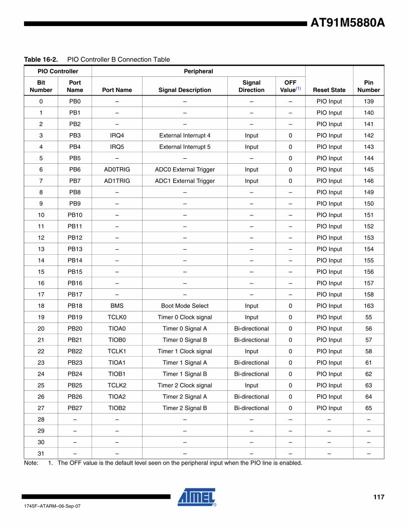
AT91M5880A
Note: 1. The OFF value is the default level seen on the peripheral input when the PIO line is enabled.
Table 16-2. PIO Controller B Connection Table
PIO Controller Peripheral
Reset StatePin
NumberBit
NumberPort
Name Port Name Signal DescriptionSignal
DirectionOFF
Value(1)
0 PB0 – – – – PIO Input 139
1 PB1 – – – – PIO Input 140
2 PB2 – – – – PIO Input 141
3 PB3 IRQ4 External Interrupt 4 Input 0 PIO Input 142
4 PB4 IRQ5 External Interrupt 5 Input 0 PIO Input 143
5 PB5 – – – 0 PIO Input 144
6 PB6 AD0TRIG ADC0 External Trigger Input 0 PIO Input 145
7 PB7 AD1TRIG ADC1 External Trigger Input 0 PIO Input 146
8 PB8 – – – – PIO Input 149
9 PB9 – – – – PIO Input 150
10 PB10 – – – – PIO Input 151
11 PB11 – – – – PIO Input 152
12 PB12 – – – – PIO Input 153
13 PB13 – – – – PIO Input 154
14 PB14 – – – – PIO Input 155
15 PB15 – – – – PIO Input 156
16 PB16 – – – – PIO Input 157
17 PB17 – – – – PIO Input 158
18 PB18 BMS Boot Mode Select Input 0 PIO Input 163
19 PB19 TCLK0 Timer 0 Clock signal Input 0 PIO Input 55
20 PB20 TIOA0 Timer 0 Signal A Bi-directional 0 PIO Input 56
21 PB21 TIOB0 Timer 0 Signal B Bi-directional 0 PIO Input 57
22 PB22 TCLK1 Timer 1 Clock signal Input 0 PIO Input 58
23 PB23 TIOA1 Timer 1 Signal A Bi-directional 0 PIO Input 61
24 PB24 TIOB1 Timer 1 Signal B Bi-directional 0 PIO Input 62
25 PB25 TCLK2 Timer 2 Clock signal Input 0 PIO Input 63
26 PB26 TIOA2 Timer 2 Signal A Bi-directional 0 PIO Input 64
27 PB27 TIOB2 Timer 2 Signal B Bi-directional 0 PIO Input 65
28 – – – – – – –
29 – – – – – – –
30 – – – – – – –
31 – – – – – – –
1171745F–ATARM–06-Sep-07

16.9 PIO User InterfacePIO Controller A Base Address:0xFFFEC000 (Code Label PIOA_BASE)
PIO Controller B Base Address:0xFFFF0000 (Code Label PIOB_BASE)
Notes: 1. The reset value of this register depends on the level of the external pins at reset.
2. This register is cleared at reset. However, the first read of the register can give a value not equal to zero if any changes have occurred on any pins between the reset and the read.
Table 16-3. Register Mapping
Offset Register Name Access Reset
0x00 PIO Enable Register PIO_PER Write-only –
0x04 PIO Disable Register PIO_PDR Write-only –
0x08PIO Status Register
PIO_PSR Read-only0x3FFF FFFF (A) 0x0FFF FFFF (B)
0x0C Reserved – – –
0x10 Output Enable Register PIO_OER Write-only –
0x14 Output Disable Register PIO_ODR Write-only –
0x18 Output Status Register PIO_OSR Read-only 0
0x1C Reserved – – –
0x20 Input Filter Enable Register PIO_IFER Write-only –
0x24 Input Filter Disable Register PIO_IFDR Write-only –
0x28 Input Filter Status Register PIO_IFSR Read-only 0
0x2C Reserved – – –
0x30 Set Output Data Register PIO_SODR Write-only –
0x34 Clear Output Data Register PIO_CODR Write-only –
0x38 Output Data Status Register PIO_ODSR Read-only 0
0x3C Pin Data Status Register PIO_PDSR Read-only see Note (1)
0x40 Interrupt Enable Register PIO_IER Write-only –
0x44 Interrupt Disable Register PIO_IDR Write-only –
0x48 Interrupt Mask Register PIO_IMR Read-only 0
0x4C Interrupt Status Register PIO_ISR Read-only see Note (2)
0x50 Multi-driver Enable Register PIO_MDER Write-only –
0x54 Multi-driver Disable Register PIO_MDDR Write-only –
0x58 Multi-driver Status Register PIO_MDSR Read-only 0
0x5C Reserved – – –
1181745F–ATARM–06-Sep-07
AT91M5880A

AT91M5880A
16.9.1 PIO Enable RegisterRegister Name: PIO_PER
Access Type: Write-only
Offset: 0x00
This register is used to enable individual pins to be controlled by the PIO Controller instead of the associated peripheral.When the PIO is enabled, the associated peripheral (if any) is held at logic zero.
1 = Enables the PIO to control the corresponding pin (disables peripheral control of the pin).
0 = No effect.
16.9.2 PIO Disable RegisterRegister Name: PIO_PDR
Access Type: Write-only
Offset: 0x04
This register is used to disable PIO control of individual pins. When the PIO control is disabled, the normal peripheral func-tion is enabled on the corresponding pin.
1 = Disables PIO control (enables peripheral control) on the corresponding pin.
0 = No effect.
31 30 29 28 27 26 25 24
P31 P30 P29 P28 P27 P26 P25 P24
23 22 21 20 19 18 17 16
P23 P22 P21 P20 P19 P18 P17 P16
15 14 13 12 11 10 9 8
P15 P14 P13 P12 P11 P10 P9 P8
7 6 5 4 3 2 1 0
P7 P6 P5 P4 P3 P2 P1 P0
31 30 29 28 27 26 25 24
P31 P30 P29 P28 P27 P26 P25 P24
23 22 21 20 19 18 17 16
P23 P22 P21 P20 P19 P18 P17 P16
15 14 13 12 11 10 9 8
P15 P14 P13 P12 P11 P10 P9 P8
7 6 5 4 3 2 1 0
P7 P6 P5 P4 P3 P2 P1 P0
1191745F–ATARM–06-Sep-07

16.9.3 PIO Status RegisterRegister Name: PIO_PSR
Access Type: Read-only
Offset: 0x08
Reset Value: 0x3FFFFFFF (A)
0x0FFFFFFF (B)
This register indicates which pins are enabled for PIO control. This register is updated when PIO lines are enabled ordisabled.
1 = PIO is active on the corresponding line (peripheral is inactive).
0 = PIO is inactive on the corresponding line (peripheral is active).
16.9.4 PIO Output Enable Register Register Name: PIO_OER
Access Type: Write-only
Offset: 0x10
This register is used to enable PIO output drivers. If the pin is driven by a peripheral, this has no effect on the pin, but theinformation is stored. The register is programmed as follows:
1 = Enables the PIO output on the corresponding pin.
0 = No effect.
31 30 29 28 27 26 25 24
P31 P30 P29 P28 P27 P26 P25 P24
23 22 21 20 19 18 17 16
P23 P22 P21 P20 P19 P18 P17 P16
15 14 13 12 11 10 9 8
P15 P14 P13 P12 P11 P10 P9 P8
7 6 5 4 3 2 1 0
P7 P6 P5 P4 P3 P2 P1 P0
31 30 29 28 27 26 25 24
P31 P30 P29 P28 P27 P26 P25 P24
23 22 21 20 19 18 17 16
P23 P22 P21 P20 P19 P18 P17 P16
15 14 13 12 11 10 9 8
P15 P14 P13 P12 P11 P10 P9 P8
7 6 5 4 3 2 1 0
P7 P6 P5 P4 P3 P2 P1 P0
1201745F–ATARM–06-Sep-07
AT91M5880A

AT91M5880A
16.9.5 PIO Output Disable RegisterRegister Name: PIO_ODR
Access Type: Write-only
Offset: 0x14
This register is used to disable PIO output drivers. If the pin is driven by the peripheral, this has no effect on the pin, but theinformation is stored. The register is programmed as follows:
1 = Disables the PIO output on the corresponding pin.
0 = No effect.
16.9.6 PIO Output Status RegisterRegister Name: PIO_OSR
Access Type: Read-only
Offset: 0x18
Reset Value: 0
This register shows the PIO pin control (output enable) status which is programmed in PIO_OER and PIO ODR. Thedefined value is effective only if the pin is controlled by the PIO. The register reads as follows:
1 = The corresponding PIO is output on this line.
0 = The corresponding PIO is input on this line.
31 30 29 28 27 26 25 24
P31 P30 P29 P28 P27 P26 P25 P24
23 22 21 20 19 18 17 16
P23 P22 P21 P20 P19 P18 P17 P16
15 14 13 12 11 10 9 8
P15 P14 P13 P12 P11 P10 P9 P8
7 6 5 4 3 2 1 0
P7 P6 P5 P4 P3 P2 P1 P0
31 30 29 28 27 26 25 24
P31 P30 P29 P28 P27 P26 P25 P24
23 22 21 20 19 18 17 16
P23 P22 P21 P20 P19 P18 P17 P16
15 14 13 12 11 10 9 8
P15 P14 P13 P12 P11 P10 P9 P8
7 6 5 4 3 2 1 0
P7 P6 P5 P4 P3 P2 P1 P0
1211745F–ATARM–06-Sep-07

16.9.7 PIO Input Filter Enable RegisterRegister Name: PIO_IFER
Access Type: Write-only
Offset: 0x20
This register is used to enable input glitch filters. It affects the pin whether or not the PIO is enabled. The register is pro-grammed as follows:
1 = Enables the glitch filter on the corresponding pin.
0 = No effect.
16.9.8 PIO Input Filter Disable RegisterRegister Name: IO_IFDR
Access Type: Write-only
Offset: 0x24
This register is used to disable input glitch filters. It affects the pin whether or not the PIO is enabled. The register is pro-grammed as follows:
1 = Disables the glitch filter on the corresponding pin.
0 = No effect.
31 30 29 28 27 26 25 24
P31 P30 P29 P28 P27 P26 P25 P24
23 22 21 20 19 18 17 16
P23 P22 P21 P20 P19 P18 P17 P16
15 14 13 12 11 10 9 8
P15 P14 P13 P12 P11 P10 P9 P8
7 6 5 4 3 2 1 0
P7 P6 P5 P4 P3 P2 P1 P0
31 30 29 28 27 26 25 24
P31 P30 P29 P28 P27 P26 P25 P24
23 22 21 20 19 18 17 16
P23 P22 P21 P20 P19 P18 P17 P16
15 14 13 12 11 10 9 8
P15 P14 P13 P12 P11 P10 P9 P8
7 6 5 4 3 2 1 0
P7 P6 P5 P4 P3 P2 P1 P0
1221745F–ATARM–06-Sep-07
AT91M5880A

AT91M5880A
16.9.9 PIO Input Filter Status RegisterRegister Name: PIO_IFSR
Access Type: Read-only
Offset: 0x28
Reset Value: 0
This register indicates which pins have glitch filters selected. It is updated when PIO outputs are enabled or disabled bywriting to PIO_IFER or PIO_IFDR.
1 = Filter is selected on the corresponding input (peripheral and PIO).
0 = Filter is not selected on the corresponding input.
Note: When the glitch filter is selected, and the PIO Controller clock is disabled, either the signal on the peripheral input or the corre-sponding bit in PIO_PDSR remains at the current state.
16.9.10 PIO Set Output Data RegisterRegister Name: PIO_SODR
Access Type: Write-only
Offset: 0x30
This register is used to set PIO output data. It affects the pin only if the corresponding PIO output line is enabled and if thepin is controlled by the PIO. Otherwise, the information is stored.
1 = PIO output data on the corresponding pin is set.
0 = No effect.
31 30 29 28 27 26 25 24
P31 P30 P29 P28 P27 P26 P25 P24
23 22 21 20 19 18 17 16
P23 P22 P21 P20 P19 P18 P17 P16
15 14 13 12 11 10 9 8
P15 P14 P13 P12 P11 P10 P9 P8
7 6 5 4 3 2 1 0
P7 P6 P5 P4 P3 P2 P1 P0
31 30 29 28 27 26 25 24
P31 P30 P29 P28 P27 P26 P25 P24
23 22 21 20 19 18 17 16
P23 P22 P21 P20 P19 P18 P17 P16
15 14 13 12 11 10 9 8
P15 P14 P13 P12 P11 P10 P9 P8
7 6 5 4 3 2 1 0
P7 P6 P5 P4 P3 P2 P1 P0
1231745F–ATARM–06-Sep-07

16.9.11 PIO Clear Output Data RegisterRegister Name: PIO_CODR
Access Type: Write-only
Offset: 0x34
This register is used to clear PIO output data. It affects the pin only if the corresponding PIO output line is enabled and if thepin is controlled by the PIO. Otherwise, the information is stored.
1 = PIO output data on the corresponding pin is cleared.
0 = No effect.
16.9.12 PIO Output Data Status RegisterRegister Name: PIO_ODSR
Access Type: Read-only
Offset: 0x38
Reset Value: 0
This register shows the output data status which is programmed in PIO_SODR or PIO_CODR. The defined value is effec-tive only if the pin is controlled by the PIO Controller and only if the pin is defined as an output.
1 = The output data for the corresponding line is programmed to 1.
0 = The output data for the corresponding line is programmed to 0.
31 30 29 28 27 26 25 24
P31 P30 P29 P28 P27 P26 P25 P24
23 22 21 20 19 18 17 16
P23 P22 P21 P20 P19 P18 P17 P16
15 14 13 12 11 10 9 8
P15 P14 P13 P12 P11 P10 P9 P8
7 6 5 4 3 2 1 0
P7 P6 P5 P4 P3 P2 P1 P0
31 30 29 28 27 26 25 24
P31 P30 P29 P28 P27 P26 P25 P24
23 22 21 20 19 18 17 16
P23 P22 P21 P20 P19 P18 P17 P16
15 14 13 12 11 10 9 8
P15 P14 P13 P12 P11 P10 P9 P8
7 6 5 4 3 2 1 0
P7 P6 P5 P4 P3 P2 P1 P0
1241745F–ATARM–06-Sep-07
AT91M5880A

AT91M5880A
16.9.13 PIO Pin Data Status RegisterRegister Name: PIO_PDSR
Access Type: Read-only
Offset: 0x3C
Reset Value: Undefined
This register shows the state of the physical pin of the chip. The pin values are always valid, regardless of whether the pinsare enabled as PIO, peripheral, input or output. The register reads as follows:
1 = The corresponding pin is at logic 1.
0 = The corresponding pin is at logic 0.
16.9.14 PIO Interrupt Enable RegisterRegister Name: PIO_IER
Access Type: Write-only
Offset: 0x40
This register is used to enable PIO interrupts on the corresponding pin. It has effect whether PIO is enabled or not.
1 = Enables an interrupt when a change of logic level is detected on the corresponding pin.
0 = No effect.
31 30 29 28 27 26 25 24
P31 P30 P29 P28 P27 P26 P25 P24
23 22 21 20 19 18 17 16
P23 P22 P21 P20 P19 P18 P17 P16
15 14 13 12 11 10 9 8
P15 P14 P13 P12 P11 P10 P9 P8
7 6 5 4 3 2 1 0
P7 P6 P5 P4 P3 P2 P1 P0
31 30 29 28 27 26 25 24
P31 P30 P29 P28 P27 P26 P25 P24
23 22 21 20 19 18 17 16
P23 P22 P21 P20 P19 P18 P17 P16
15 14 13 12 11 10 9 8
P15 P14 P13 P12 P11 P10 P9 P8
7 6 5 4 3 2 1 0
P7 P6 P5 P4 P3 P2 P1 P0
1251745F–ATARM–06-Sep-07

16.9.15 PIO Interrupt Disable RegisterRegister Name: PIO_IDR
Access Type: Write-only
Offset: 0x44
This register is used to disable PIO interrupts on the corresponding pin. It has effect whether the PIO is enabled or not.
1 = Disables the interrupt on the corresponding pin. Logic level changes are still detected.
0 = No effect.
16.9.16 PIO Interrupt Mask RegisterRegister Name: PIO_IMR
Access Type: Read-only
Offset: 0x48
Reset Value: 0
This register shows which pins have interrupts enabled. It is updated when interrupts are enabled or disabled by writing toPIO_IER or PIO_IDR.
1 = Interrupt is enabled on the corresponding input pin.
0 = Interrupt is not enabled on the corresponding input pin.
31 30 29 28 27 26 25 24
P31 P30 P29 P28 P27 P26 P25 P24
23 22 21 20 19 18 17 16
P23 P22 P21 P20 P19 P18 P17 P16
15 14 13 12 11 10 9 8
P15 P14 P13 P12 P11 P10 P9 P8
7 6 5 4 3 2 1 0
P7 P6 P5 P4 P3 P2 P1 P0
31 30 29 28 27 26 25 24
P31 P30 P29 P28 P27 P26 P25 P24
23 22 21 20 19 18 17 16
P23 P22 P21 P20 P19 P18 P17 P16
15 14 13 12 11 10 9 8
P15 P14 P13 P12 P11 P10 P9 P8
7 6 5 4 3 2 1 0
P7 P6 P5 P4 P3 P2 P1 P0
1261745F–ATARM–06-Sep-07
AT91M5880A

AT91M5880A
16.9.17 PIO Interrupt Status RegisterRegister Name: PIO_ISR
Access Type: Read-only
Offset: 0x4C
Reset Value: 0
This register indicates for each pin when a logic value change has been detected (rising or falling edge). This is validwhether the PIO is selected for the pin or not and whether the pin is an input or an output.
The register is reset to zero following a read, and at reset.
1 = At least one input change has been detected on the corresponding pin since the register was last read.
0 = No input change has been detected on the corresponding pin since the register was last read.
16.9.18 PIO Multi-driver Enable RegisterRegister Name: PIO_MDER
Access Type: Write-only
Offset: 0x50
This register is used to enable PIO output drivers to be configured as open drain to support external drivers on the samepin.
1 = Enables multi-drive option on the corresponding pin.
0 = No effect.
31 30 29 28 27 26 25 24
P31 P30 P29 P28 P27 P26 P25 P24
23 22 21 20 19 18 17 16
P23 P22 P21 P20 P19 P18 P17 P16
15 14 13 12 11 10 9 8
P15 P14 P13 P12 P11 P10 P9 P8
7 6 5 4 3 2 1 0
P7 P6 P5 P4 P3 P2 P1 P0
31 30 29 28 27 26 25 24
P31 P30 P29 P28 P27 P26 P25 P24
23 22 21 20 19 18 17 16
P23 P22 P21 P20 P19 P18 P17 P16
15 14 13 12 11 10 9 8
P15 P14 P13 P12 P11 P10 P9 P8
7 6 5 4 3 2 1 0
P7 P6 P5 P4 P3 P2 P1 P0
1271745F–ATARM–06-Sep-07

16.9.19 PIO Multi-driver Disable RegisterRegister Name: PIO_MDDR
Access Type: Write-only
Offset: 0x54
This register is used to disable the open drain configuration of the output buffer.
1 = Disables the multi-driver option on the corresponding pin.
0 = No effect.
16.9.20 PIO Multi-driver Status RegisterRegister Name: PIO_MDSR
Access Type: Read-only
Reset Value: 0x0
Offset: 0x58
This register indicates which pins are configured with open drain drivers.
1 = PIO is configured as an open drain.
0 = PIO is not configured as an open drain.
31 30 29 28 27 26 25 24
P31 P30 P29 P28 P27 P26 P25 P24
23 22 21 20 19 18 17 16
P23 P22 P21 P20 P19 P18 P17 P16
15 14 13 12 11 10 9 8
P15 P14 P13 P12 P11 P10 P9 P8
7 6 5 4 3 2 1 0
P7 P6 P5 P4 P3 P2 P1 P0
31 30 29 28 27 26 25 24
P31 P30 P29 P28 P27 P26 P25 P24
23 22 21 20 19 18 17 16
P23 P22 P21 P20 P19 P18 P17 P16
15 14 13 12 11 10 9 8
P15 P14 P13 P12 P11 P10 P9 P8
7 6 5 4 3 2 1 0
P7 P6 P5 P4 P3 P2 P1 P0
1281745F–ATARM–06-Sep-07
AT91M5880A

AT91M5880A
17. SF: Special Function RegistersThe AT91M55800A provides registers which implement the following special functions.
• Chip identification
• RESET status
17.1 Chip IdentifierThe following chip identifier values are covered in this datasheet:
17.2 SF User InterfaceChip ID Base Address = 0xFFF00000 (Code Label SF_BASE)
Product Revision Chip ID
AT91M55800A A 0x15580040
Table 17-1. Register Mapping
Offset Register Name Access Reset State
0x00 Chip ID Register SF_CIDR Read-only Hardwired
0x04 Chip ID Extension Register SF_EXID Read-only Hardwired
0x08 Reset Status Register SF_RSR Read-onlySee register description
0x0C Reserved – – –
0x10 Reserved – – –
0x14 Reserved – – –
0x18 Protect Mode Register SF_PMR Read/Write 0x0
1291745F–ATARM–06-Sep-07

17.2.1 Chip ID RegisterRegister Name: SF_CIDR
Access Type: Read-only
Offset: 0x00
• VERSION: Version of the chip (Code Label SF_VERSION)This value is incremented by one with each new version of the chip (from zero to a maximum value of 31).
• NVPSIZ: Nonvolatile Program Memory Size
• NVDSIZ: Nonvolatile Data Memory Size
• VDSIZ: Volatile Data Memory Size
31 30 29 28 27 26 25 24
EXT NVPTYP ARCH
23 22 21 20 19 18 17 16
ARCH VDSIZ
15 14 13 12 11 10 9 8
NVDSIZ NVPSIZ
7 6 5 4 3 2 1 0
0 1 0 VERSION
NVPSIZ Size Code Label: SF_NVPSIZ
0 0 0 0 None SF_NVPSIZ_NONE
0 0 1 1 32K Bytes SF_NVPSIZ_32K
0 1 0 1 64K Bytes SF_NVP_SIZ_64K
0 1 1 1 128K Bytes SF_NVP_SIZ_128K
1 0 0 1 256K Bytes SF_NVP_SIZ_256K
Others Reserved –
NVDSIZ Size Code Label: SF_NVDSIZ
0 0 0 0 None SF_NVDSIZ_NONE
Others Reserved –
VDSIZ Size Code Label: SF_VDSIZ
0 0 0 0 None SF_VDSIZ_NONE
0 0 0 1 1K Bytes SF_VDSIZ_1K
0 0 1 0 2K Bytes SF_VDSIZ_2K
0 1 0 0 4K Bytes SF_VDSIZ_4K
1 0 0 0 8K Bytes SF_VDSIZ_8K
Others Reserved –
1301745F–ATARM–06-Sep-07
AT91M5880A

AT91M5880A
• ARCH: Chip Architecture Code of Architecture: Two BCD digits
• NVPTYP: Nonvolatile Program Memory Type
Note: All other codes are reserved.
• EXT: Extension Flag (Code Label SF_EXT)0 = Chip ID has a single-register definition without extensions
1 = An extended Chip ID exists (to be defined in the future).
17.2.2 Chip ID Extension Register Register Name: SF_EXID
Access Type: Read-only
Offset: 0x04
This register is reserved for future use. It will be defined when needed.
ARCH Selected ARCH Code Label: SF_ARCH
0110 0011 AT91x63yyy SF_ARCH_AT91x63
0100 0000 AT91x40yyy SF_ARCH_AT91x40
0101 0101 AT91x55yyy SF_ARCH_AT91x55
NVPTYP Type Code Label: SF_NVPTYP
0 0 1 “M” Series or “F” Series SF_NVPTYP_M
1 0 0 “R” Series SF_NVPTYP_R
1311745F–ATARM–06-Sep-07

17.2.3 Reset Status RegisterRegister Name: SF_RSR
Access Type: Read-only
Offset: 0x08
• RESET: Reset Status InformationThis field indicates whether the reset was demanded by the external system (via NRST) or by the Watchdog internal resetrequest.
31 30 29 28 27 26 25 24
– – – – – – – –
23 22 21 20 19 18 17 16
– – – – – – – –
15 14 13 12 11 10 9 8
– – – – – – – –
7 6 5 4 3 2 1 0
RESET
Reset Cause of Reset Code Label
0x6C External Pin SF_EXT_RESET
0x53 Internal Watchdog SF_WD_RESET
1321745F–ATARM–06-Sep-07
AT91M5880A

AT91M5880A
17.2.4 SF Protect Mode RegisterRegister Name: SF_PMR
Access Type: Read/Write
Reset Value: 0x0
Offset: 0x18
• PMRKEY: Protect Mode Register KeyUsed only when writing SF_PMR. PMRKEY is reads 0.
0x27A8: Write access in SF_PMR is allowed.
Other value: Write access in SF_PMR is prohibited.
• AIC: AIC Protect Mode Enable (Code Label SF_AIC)0 = The Advanced Interrupt Controller runs in Normal Mode.
1 = The Advanced Interrupt Controller runs in Protect Mode.
31 30 29 28 27 26 25 24
PMRKEY
23 22 21 20 19 18 17 16
PMRKEY
15 14 13 12 11 10 9 8
– – – – – – – –
7 6 5 4 3 2 1 0
– – AIC – – – – –
1331745F–ATARM–06-Sep-07

18. USART: Universal Synchronous/ Asynchronous Receiver/TransmitterThe AT91M55800AA provides three identical, full-duplex, universal synchronous/asynchronousreceiver/transmitters which are connected to the Peripheral Data Controller.
The main features are:
• Programmable Baud Rate Generator
• Parity, Framing and Overrun Error Detection
• Line Break Generation and Detection
• Automatic Echo, Local Loopback and Remote Loopback channel modes
• Multi-drop Mode: Address Detection and Generation
• Interrupt Generation
• Two Dedicated Peripheral Data Controller channels
• 5-, 6-, 7-, 8- and 9-bit character length
Figure 18-1. USART Block Diagram
Peripheral Data Controller
ReceiverChannel
TransmitterChannel
Control Logic
Interrupt Control
Baud Rate Generator
Receiver
Transmitter
AMBA
ASB
APB
USxIRQ
MCK
MCK/8
RXD
TXD
SCK
USART Channel
Baud Rate Clock
PIO: Parallel
I/O Controller
1341745F–ATARM–06-Sep-07
AT91M5880A

AT91M5880A
18.1 Pin Description
Notes: 1. After a hardware reset, the USART clock is disabled by default. The user must configure the Power Management Controller before any access to the User Interface of the USART.
2. After a hardware reset, the USART pins are deselected by default (see Section 16. “PIO: Parallel I/O Controller” on page 113). The user must configure the PIO Controller before enabling the transmitter or receiver. If the user selects one of the internal clocks, SCK can be configured as a PIO.
Table 18-1. USART Channel External Signals
Name Description
SCKUSART Serial clock can be configured as input or output:SCK is configured as input if an External clock is selected (USCLKS[1] = 1)SCK is driven as output if the External Clock is disabled (USCLKS[1] = 0) and Clock output is enabled (CLKO = 1)
TXD Transmit Serial Data is an output
RXD Receive Serial Data is an input
1351745F–ATARM–06-Sep-07

18.2 Baud Rate Generator The Baud Rate Generator provides the bit period clock (the Baud Rate clock) to both theReceiver and the Transmitter.
The Baud Rate Generator can select between external and internal clock sources. The externalclock source is SCK. The internal clock sources can be either the master clock MCK or the mas-ter clock divided by 8 (MCK/8).
Note: In all cases, if an external clock is used, the duration of each of its levels must be longer than the system clock (MCK) period. The external clock frequency must be at least 2.5 times lower than the system clock.
When the USART is programmed to operate in Asynchronous Mode (SYNC = 0 in the ModeRegister US_MR), the selected clock is divided by 16 times the value (CD) written in US_BRGR(Baud Rate Generator Register). If US_BRGR is set to 0, the Baud Rate Clock is disabled.
When the USART is programmed to operate in Synchronous Mode (SYNC = 1) and the selectedclock is internal (USCLKS[1] = 0 in the Mode Register US_MR), the Baud Rate Clock is theinternal selected clock divided by the value written in US_BRGR. If US_BRGR is set to 0, theBaud Rate Clock is disabled.
In Synchronous Mode with external clock selected (USCLKS[1] = 1), the clock is provideddirectly by the signal on the SCK pin. No division is active. The value written in US_BRGR hasno effect.
Figure 18-2. Baud Rate Generator
Baud Rate =Selected Clock
16 x CD
Baud Rate =Selected Clock
CD
USCLKS [1]
0
01
1
MCK
MCK/8
SCK
CLK16-bit Counter
0
0
1Baud Rate
Clock
SYNC
USCLKS [1]
CD
CD
OUT
0
1
Divide by 16
SYNC
0
1
>1
USCLKS [0]
1361745F–ATARM–06-Sep-07
AT91M5880A

AT91M5880A
18.3 Receiver
18.3.1 Asynchronous ReceiverThe USART is configured for asynchronous operation when SYNC = 0 (bit 7 of US_MR). Inasynchronous mode, the USART detects the start of a received character by sampling the RXDsignal until it detects a valid start bit. A low level (space) on RXD is interpreted as a valid start bitif it is detected for more than 7 cycles of the sampling clock, which is 16 times the baud rate.Hence a space which is longer than 7/16 of the bit period is detected as a valid start bit. A spacewhich is 7/16 of a bit period or shorter is ignored and the receiver continues to wait for a validstart bit.
When a valid start bit has been detected, the receiver samples the RXD at the theoretical mid-point of each bit. It is assumed that each bit lasts 16 cycles of the sampling clock (one bit period)so the sampling point is 8 cycles (0.5-bit periods) after the start of the bit. The first sampling pointis therefore 24 cycles (1.5-bit periods) after the falling edge of the start bit was detected. Eachsubsequent bit is sampled 16 cycles (1-bit period) after the previous one.
Figure 18-3. Asynchronous Mode: Start Bit Detection
Figure 18-4. Asynchronous Mode: Character Reception
16 x BaudRate Clock
RXD
True Start Detection
D0Sampling
D0 D1 D2 D3 D4 D5 D6 D7
RXD
True Start DetectionSampling
Parity BitStop Bit
Example: 8-bit, parity enabled 1 stop
1-bit period
0.5-bit periods
1371745F–ATARM–06-Sep-07

18.3.2 Synchronous ReceiverWhen configured for synchronous operation (SYNC = 1), the receiver samples the RXD signalon each rising edge of the Baud Rate clock. If a low level is detected, it is considered as a start.Data bits, parity bit and stop bit are sampled and the receiver waits for the next start bit. Seeexample in Figure 18-5.
Figure 18-5. Synchronous Mode: Character Reception
18.3.3 Receiver ReadyWhen a complete character is received, it is transferred to the US_RHR and the RXRDY statusbit in US_CSR is set. If US_RHR has not been read since the last transfer, the OVRE status bitin US_CSR is set.
18.3.4 Parity ErrorEach time a character is received, the receiver calculates the parity of the received data bits, inaccordance with the field PAR in US_MR. It then compares the result with the received parity bit.If different, the parity error bit PARE in US_CSR is set. When the character is completed and assoon as the character is read, the parity status bit is cleared.
18.3.5 Framing ErrorIf a character is received with a stop bit at low level and with at least one data bit at high level, aframing error is generated. This sets FRAME in US_CSR.
18.3.6 Time-outThis function allows an idle condition on the RXD line to be detected. The maximum delay forwhich the USART should wait for a new character to arrive while the RXD line is inactive (highlevel) is programmed in US_RTOR (Receiver Time-out). When this register is set to 0, no time-out is detected. Otherwise, the receiver waits for a first character and then initializes a counterwhich is decremented at each bit period and reloaded at each byte reception. When the counterreaches 0, the TIMEOUT bit in US_CSR is set. The user can restart the wait for a first characterwith the STTTO (Start Time-out) bit in US_CR.
Calculation of time-out duration:
D0 D1 D2 D3 D4 D5 D6 D7
RXD
True Start DetectionSampling
Parity BitStop Bit
Example: 8-bit, parity enabled 1 stop
SCK
Duration Value 4 BitPeriod••=
1381745F–ATARM–06-Sep-07
AT91M5880A

AT91M5880A
18.4 TransmitterThe transmitter has the same behavior in both synchronous and asynchronous operatingmodes. Start bit, data bits, parity bit and stop bits are serially shifted, lowest significant bit first,on the falling edge of the serial clock. See example in Figure 18-6.
The number of data bits is selected in the CHRL field in US_MR.
The parity bit is set according to the PAR field in US_MR.
The number of stop bits is selected in the NBSTOP field in US_MR.
When a character is written to US_THR (Transmit Holding), it is transferred to the Shift Registeras soon as it is empty. When the transfer occurs, the TXRDY bit in US_CSR is set until a newcharacter is written to US_THR. If Transmit Shift Register and US_THR are both empty, theTXEMPTY bit in US_CSR is set.
18.4.1 Time-guardThe Time-guard function allows the transmitter to insert an idle state on the TXD line betweentwo characters. The duration of the idle state is programmed in US_TTGR (Transmitter Time-guard). When this register is set to zero, no time-guard is generated. Otherwise, the transmitterholds a high level on TXD after each transmitted byte during the number of bit periods pro-grammed in US_TTGR.
18.5 Multi-drop Mode When the field PAR in US_MR equals 11X (binary value), the USART is configured to run inmulti-drop mode. In this case, the parity error bit PARE in US_CSR is set when data is detectedwith a parity bit set to identify an address byte. PARE is cleared with the Reset Status Bits Com-mand (RSTSTA) in US_CR. If the parity bit is detected low, identifying a data byte, PARE is notset.
The transmitter sends an address byte (parity bit set) when a Send Address Command(SENDA) is written to US_CR. In this case, the next byte written to US_THR will be transmittedas an address. After this any byte transmitted will have the parity bit cleared.
Figure 18-6. Synchronous and Asynchronous Modes: Character Transmission
Idle state durationbetween two characters
Time-guardvalue
Bitperiod•=
D0 D1 D2 D3 D4 D5 D6 D7
TXD
Start Bit
ParityBit
StopBit
Example: 8-bit, parity enabled 1 stop
Baud Rate Clock
1391745F–ATARM–06-Sep-07

18.6 Break A break condition is a low signal level which has a duration of at least one character (includingstart/stop bits and parity).
18.6.1 Transmit BreakThe transmitter generates a break condition on the TXD line when STTBRK is set in US_CR(Control Register). In this case, the character present in the Transmit Shift Register is completedbefore the line is held low.
To cancel a break condition on the TXD line, the STPBRK command in US_CR must be set. TheUSART completes a minimum break duration of one character length. The TXD line then returnsto high level (idle state) for at least 12-bit periods to ensure that the end of break is correctlydetected. Then the transmitter resumes normal operation.
The BREAK is managed like a character:
• The STTBRK and the STPBRK commands are performed only if the transmitter is ready (bit TXRDY = 1 in US_CSR)
• The STTBRK command blocks the transmitter holding register (bit TXRDY is cleared in US_CSR) until the break has started
• A break is started when the Shift Register is empty (any previous character is fully transmitted). US_CSR.TXEMPTY is cleared. The break blocks the transmitter shift register until it is completed (high level for at least 12-bit periods after the STPBRK command is requested)
In order to avoid unpredictable states:
• STTBRK and STPBRK commands must not be requested at the same time
• Once an STTBRK command is requested, further STTBRK commands are ignored until the BREAK is ended (high level for at least 12-bit periods)
• All STPBRK commands requested without a previous STTBRK command are ignored
• A byte written into the Transmit Holding Register while a break is pending but not started (bit TXRDY = 0 in US_CSR) is ignored
• It is not permitted to write new data in the Transmit Holding Register while a break is in progress (STPBRK has not been requested), even though TXRDY = 1 in US_CSR.
• A new STTBRK command must not be issued until an existing break has ended (TXEMPTY=1 in US_CSR).
1401745F–ATARM–06-Sep-07
AT91M5880A

AT91M5880A
The standard break transmission sequence is:
1. Wait for the transmitter ready (US_CSR.TXRDY = 1)
2. Send the STTBRK command(write 0x0200 to US_CR)
3. Wait for the transmitter ready(bit TXRDY = 1 in US_CSR)
4. Send the STPBRK command(write 0x0400 to US_CR)
The next byte can then be sent:
5. Wait for the transmitter ready(bit TXRDY = 1 in US_CSR)
6. Send the next byte(write byte to US_THR)
Each of these steps can be scheduled by using the interrupt if the bit TXRDY in US_IMR is set.
For character transmission, the USART channel must be enabled before sending a break.
18.6.2 Receive BreakThe receiver detects a break condition when all data, parity and stop bits are low. When the lowstop bit is detected, the receiver asserts the RXBRK bit in US_CSR. An end of receive break isdetected by a high level for at least 1-bit + 1/16 of a bit period in asynchronous operating modeor at least one sample in synchronous operating mode. RXBRK is also asserted when an end ofbreak is detected.
Both the beginning and the end of a break can be detected by interrupt i f the bitUS_IMR.RXBRK is set.
1411745F–ATARM–06-Sep-07

18.7 Peripheral Data ControllerEach USART channel is closely connected to a corresponding Peripheral Data Controller chan-nel. One is dedicated to the receiver. The other is dedicated to the transmitter.
Note: The PDC is disabled if 9-bit character length is selected (MODE9 = 1) in US_MR.
The PDC channel is programmed using US_TPR (Transmit Pointer) and US_TCR (TransmitCounter) for the transmitter and US_RPR (Receive Pointer) and US_RCR (Receive Counter) forthe receiver. The status of the PDC is given in US_CSR by the ENDTX bit for the transmitter andby the ENDRX bit for the receiver.
The pointer registers (US_TPR and US_RPR) are used to store the address of the transmit orreceive buffers. The counter registers (US_TCR and US_RCR) are used to store the size ofthese buffers.
The receiver data transfer is triggered by the RXRDY bit and the transmitter data transfer is trig-gered by TXRDY. When a transfer is performed, the counter is decremented and the pointer isincremented. When the counter reaches 0, the status bit is set (ENDRX for the receiver, ENDTXfor the transmitter in US_CSR) and can be programmed to generate an interrupt. Transfers arethen disabled until a new non-zero counter value is programmed.
18.8 Interrupt GenerationEach status bit in US_CSR has a corresponding bit in US_IER (Interrupt Enable) and US_IDR(Interrupt Disable) which controls the generation of interrupts by asserting the USART interruptline connected to the Advanced Interrupt Controller. US_IMR (Interrupt Mask Register) indicatesthe status of the corresponding bits.
When a bit is set in US_CSR and the same bit is set in US_IMR, the interrupt line is asserted.
18.9 Channel ModesThe USART can be programmed to operate in three different test modes, using the fieldCHMODE in US_MR.
Automatic echo mode allows bit by bit re-transmission. When a bit is received on the RXD line, itis sent to the TXD line. Programming the transmitter has no effect.
Local loopback mode allows the transmitted characters to be received. TXD and RXD pins arenot used and the output of the transmitter is internally connected to the input of the receiver. TheRXD pin level has no effect and the TXD pin is held high, as in idle state.
Remote loopback mode directly connects the RXD pin to the TXD pin. The Transmitter and theReceiver are disabled and have no effect. This mode allows bit by bit re-transmission.
1421745F–ATARM–06-Sep-07
AT91M5880A

AT91M5880A
Figure 18-7. Channel Modes
Receiver
TransmitterDisabled
RXD
TXD
Receiver
TransmitterDisabled
RXD
TXD
VDD
Disabled
Receiver
TransmitterDisabled
RXD
TXD
Disabled
Automatic Echo
Local Loopback
Remote Loopback VDD
1431745F–ATARM–06-Sep-07

18.10 USART User InterfaceBase Address USART0: 0xFFFC0000 (Code Label USART0_BASE)Base Address USART1: 0xFFFC4000 (Code Label USART1_BASE)Base Address USART2: 0xFFFC8000 (Code Label USART2_BASE)
Table 18-2. Register Mapping
Offset Register Name Access Reset
0x00 Control Register US_CR Write-only –
0x04 Mode Register US_MR Read/Write 0
0x08 Interrupt Enable Register US_IER Write-only –
0x0C Interrupt Disable Register US_IDR Write-only –
0x10 Interrupt Mask Register US_IMR Read-only 0
0x14 Channel Status Register US_CSR Read-only 0x18
0x18 Receiver Holding Register US_RHR Read-only 0
0x1C Transmitter Holding Register US_THR Write-only –
0x20 Baud Rate Generator Register US_BRGR Read/Write 0
0x24 Receiver Time-out Register US_RTOR Read/Write 0
0x28 Transmitter Time-guard Register US_TTGR Read/Write 0
0x2C Reserved – – –
0x30 Receive Pointer Register US_RPR Read/Write 0
0x34 Receive Counter Register US_RCR Read/Write 0
0x38 Transmit Pointer Register US_TPR Read/Write 0
0x3C Transmit Counter Register US_TCR Read/Write 0
1441745F–ATARM–06-Sep-07
AT91M5880A

AT91M5880A
18.10.1 USART Control RegisterName: US_CRAccess Type: Write-onlyOffset: 0x00
• RSTRX: Reset Receiver (Code Label US_RSTRX)0 = No effect.
1 = The receiver logic is reset.
• RSTTX: Reset Transmitter (Code Label US_RSTTX)0 = No effect.
1 = The transmitter logic is reset.
• RXEN: Receiver Enable (Code Label US_RXEN)0 = No effect.
1 = The receiver is enabled if RXDIS is 0.
• RXDIS: Receiver Disable (Code Label US_RXDIS)0 = No effect.
1 = The receiver is disabled.
• TXEN: Transmitter Enable (Code Label US_TXEN)0 = No effect.
1 = The transmitter is enabled if TXDIS is 0.
• TXDIS: Transmitter Disable (Code Label US_TXDIS)0 = No effect.
1 = The transmitter is disabled.
• RSTSTA: Reset Status Bits (Code Label US_RSTSTA)0 = No effect.
1 = Resets the status bits PARE, FRAME, OVRE and RXBRK in the US_CSR.
31 30 29 28 27 26 25 24
– – – – – – – –
23 22 21 20 19 18 17 16
– – – – – – – –
15 14 13 12 11 10 9 8
– – – SENDA STTTO STPBRK STTBRK RSTSTA
7 6 5 4 3 2 1 0
TXDIS TXEN RXDIS RXEN RSTTX RSTRX – –
1451745F–ATARM–06-Sep-07

• STTBRK: Start Break (Code Label US_STTBRK)0 = No effect.
1 = If break is not being transmitted, start transmission of a break after the characters present in US_THR and the TransmitShift Register have been transmitted.
• STPBRK: Stop Break (Code Label US_STPBRK)0 = No effect.
1 = If a break is being transmitted, stop transmission of the break after a minimum of one character length and transmit ahigh level during 12 bit periods.
• STTTO: Start Time-out (Code Label US_STTTO)0 = No effect.
1 = Start waiting for a character before clocking the time-out counter.
• SENDA: Send Address (Code Label US_SENDA)0 = No effect.
1 = In Multi-drop Mode only, the next character written to the US_THR is sent with the address bit set.
1461745F–ATARM–06-Sep-07
AT91M5880A

AT91M5880A
18.10.2 USART Mode RegisterName: US_MRAccess Type: Read/WriteReset State: 0Offset: 0x04
• USCLKS: Clock Selection (Baud Rate Generator Input Clock)
• CHRL: Character Length
Start, stop and parity bits are added to the character length.
• SYNC: Synchronous Mode Select (Code Label US_SYNC)0 = USART operates in Asynchronous Mode.
1 = USART operates in Synchronous Mode.
• PAR: Parity Type
31 30 29 28 27 26 25 24
– – – – – – – –
23 22 21 20 19 18 17 16
– – – – – CLKO MODE9 –
15 14 13 12 11 10 9 8
CHMODE NBSTOP PAR SYNC
7 6 5 4 3 2 1 0
CHRL USCLKS – – – –
USCLKS Selected Clock Code Label: US_CLKS
0 0 MCK US_CLKS_MCK
0 1 MCK/8 US_CLKS_MCK8
1 X External (SCK) US_CLKS_SCK
CHRL Character Length Code Label: US_CHRL
0 0 Five bits US_CHRL_5
0 1 Six bits US_CHRL_6
1 0 Seven bits US_CHRL_7
1 1 Eight bits US_CHRL_8
PAR Parity Type Code Label: US_PAR
0 0 0 Even Parity US_PAR_EVEN
0 0 1 Odd Parity US_PAR_ODD
0 1 0 Parity forced to 0 (Space) US_PAR_SPACE
0 1 1 Parity forced to 1 (Mark) US_PAR_MARK
1 0 x No parity US_PAR_NO
1 1 x Multi-drop mode US_PAR_MULTIDROP
1471745F–ATARM–06-Sep-07

• NBSTOP: Number of Stop BitsThe interpretation of the number of stop bits depends on SYNC.
• CHMODE: Channel Mode
• MODE9: 9-Bit Character Length (Code Label US_MODE9)0 = CHRL defines character length.
1 = 9-Bit character length.
• CKLO: Clock Output Select (Code Label US_CLKO)0 = The USART does not drive the SCK pin.
1 = The USART drives the SCK pin if USCLKS[1] is 0.
NBSTOP Asynchronous (SYNC = 0) Synchronous (SYNC = 1) Code Label: US_NBSTOP
0 0 1 stop bit 1 stop bit US_NBSTOP_1
0 1 1.5 stop bits Reserved US_NBSTOP_1_5
1 0 2 stop bits 2 stop bits US_NBSTOP_2
1 1 Reserved Reserved –
CHMODE Mode Description Code Label: US_CHMODE
0 0 Normal ModeThe USART Channel operates as an Rx/Tx USART. US_CHMODE_NORMAL
0 1 Automatic EchoReceiver Data Input is connected to TXD pin. US_CHMODE_AUTOMATIC_ECHO
1 0 Local LoopbackTransmitter Output Signal is connected to Receiver Input Signal. US_CHMODE_LOCAL_LOOPBACK
1 1 Remote LoopbackRXD pin is internally connected to TXD pin. US_CHMODE_REMODE_LOOPBACK
1481745F–ATARM–06-Sep-07
AT91M5880A

AT91M5880A
18.10.3 USART Interrupt Enable RegisterName: US_IERAccess Type: Write-onlyOffset: 0x08
• RXRDY: Enable RXRDY Interrupt (Code Label US_RXRDY)0 = No effect.
1 = Enables RXRDY Interrupt.
• TXRDY: Enable TXRDY Interrupt (Code Label US_TXRDY)0 = No effect.
1 = Enables TXRDY Interrupt.
• RXBRK: Enable Receiver Break Interrupt (Code Label US_RXBRK)0 = No effect.
1 = Enables Receiver Break Interrupt.
• ENDRX: Enable End of Receive Transfer Interrupt (Code Label US_ENDRX)0 = No effect.
1 = Enables End of Receive Transfer Interrupt.
• ENDTX: Enable End of Transmit Transfer Interrupt (Code Label US_ENDTX)0 = No effect.
1 = Enables End of Transmit Transfer Interrupt.
• OVRE: Enable Overrun Error Interrupt (Code Label US_OVRE)0 = No effect.
1 = Enables Overrun Error Interrupt.
• FRAME: Enable Framing Error Interrupt (Code Label US_FRAME)0 = No effect.
1 = Enables Framing Error Interrupt.
• PARE: Enable Parity Error Interrupt (Code Label US_PARE)0 = No effect.
1 = Enables Parity Error Interrupt.
31 30 29 28 27 26 25 24
– – – – – – – –
23 22 21 20 19 18 17 16
– – – – – – – –
15 14 13 12 11 10 9 8
– – – – – – TXEMPTY TIMEOUT
7 6 5 4 3 2 1 0
PARE FRAME OVRE ENDTX ENDRX RXBRK TXRDY RXRDY
1491745F–ATARM–06-Sep-07

• TIMEOUT: Enable Time-out Interrupt (Code Label US_TIMEOUT)0 = No effect.
1 = Enables Reception Time-out Interrupt.
• TXEMPTY: Enable TXEMPTY Interrupt (Code Label US_TXEMPTY)0 = No effect.
1 = Enables TXEMPTY Interrupt.
1501745F–ATARM–06-Sep-07
AT91M5880A

AT91M5880A
18.10.4 USART Interrupt Disable RegisterName: US_IDRAccess Type: Write-onlyOffset: 0x0C
• RXRDY: Disable RXRDY Interrupt (Code Label US_RXRDY)0 = No effect.
1 = Disables RXRDY Interrupt.
• TXRDY: Disable TXRDY Interrupt (Code Label US_TXRDY)0 = No effect.
1 = Disables TXRDY Interrupt.
• RXBRK: Disable Receiver Break Interrupt (Code Label US_RXBRK)0 = No effect.
1 = Disables Receiver Break Interrupt.
• ENDRX: Disable End of Receive Transfer Interrupt (Code Label US_ENDRX)0 = No effect.
1 = Disables End of Receive Transfer Interrupt.
• ENDTX: Disable End of Transmit Transfer Interrupt (Code Label US_ENDTX)0 = No effect.
1 = Disables End of Transmit Transfer Interrupt.
• OVRE: Disable Overrun Error Interrupt (Code Label US_OVRE)0 = No effect.
1 = Disables Overrun Error Interrupt.
• FRAME: Disable Framing Error Interrupt (Code Label US_FRAME)0 = No effect.
1 = Disables Framing Error Interrupt.
• PARE: Disable Parity Error Interrupt (Code Label US_PARE)0 = No effect.
1 = Disables Parity Error Interrupt.
31 30 29 28 27 26 25 24
– – – – – – – –
23 22 21 20 19 18 17 16
– – – – – – – –
15 14 13 12 11 10 9 8
– – – – – – TXEMPTY TIMEOUT
7 6 5 4 3 2 1 0
PARE FRAME OVRE ENDTX ENDRX RXBRK TXRDY RXRDY
1511745F–ATARM–06-Sep-07

• TIMEOUT: Disable Time-out Interrupt (Code Label US_TIMEOUT)0 = No effect.
1 = Disables Receiver Time-out Interrupt.
• TXEMPTY: Disable TXEMPTY Interrupt (Code Label US_TXEMPTY)0 = No effect.
1 = Disables TXEMPTY Interrupt.
1521745F–ATARM–06-Sep-07
AT91M5880A

AT91M5880A
18.10.5 USART Interrupt Mask RegisterName: US_IMRAccess Type: Read-onlyReset Value: 0x0Offset: 0x10
• RXRDY: RXRDY Interrupt Mask (Code Label US_RXRDY)0 = RXRDY Interrupt is Disabled.
1 = RXRDY Interrupt is Enabled.
• TXRDY: TXRDY Interrupt Mask (Code Label US_TXRDY)0 = TXRDY Interrupt is Disabled.
1 = TXRDY Interrupt is Enabled.
• RXBRK: Receiver Break Interrupt Mask (Code Label US_RXBRK)0 = Receiver Break Interrupt is Disabled.
1 = Receiver Break Interrupt is Enabled.
• ENDRX: End of Receive Transfer Interrupt Mask (Code Label US_ENDRX)0 = End of Receive Transfer Interrupt is Disabled.
1 = End of Receive Transfer Interrupt is Enabled.
• ENDTX: End of Transmit Transfer Interrupt Mask (Code Label US_ENDTX)0 = End of Transmit Transfer Interrupt is Disabled.
1 = End of Transmit Transfer Interrupt is Enabled.
• OVRE: Overrun Error Interrupt Mask (Code Label US_OVRE)0 = Overrun Error Interrupt is Disabled.
1 = Overrun Error Interrupt is Enabled.
• FRAME: Framing Error Interrupt Mask (Code Label US_FRAME)0 = Framing Error Interrupt is Disabled.
1 = Framing Error Interrupt is Enabled.
• PARE: Parity Error Interrupt Mask (Code Label US_PARE)0 = Parity Error Interrupt is Disabled.
1 = Parity Error Interrupt is Enabled.
31 30 29 28 27 26 25 24
– – – – – – – –
23 22 21 20 19 18 17 16
– – – – – – – –
15 14 13 12 11 10 9 8
– – – – – – TXEMPTY TIMEOUT
7 6 5 4 3 2 1 0
PARE FRAME OVRE ENDTX ENDRX RXBRK TXRDY RXRDY
1531745F–ATARM–06-Sep-07

• TIMEOUT: Time-out Interrupt Mask (Code Label US_TIMEOUT)0 = Receive Time-out Interrupt is Disabled.
1 = Receive Time-out Interrupt is Enabled.
• TXEMPTY: TXEMPTY Interrupt Mask (Code Label US_TXEMPTY)0 = TXEMPTY Interrupt is Disabled.
1 = TXEMPTY Interrupt is Enabled.
1541745F–ATARM–06-Sep-07
AT91M5880A

AT91M5880A
18.10.6 USART Channel Status RegisterName: US_CSRAccess Type: Read-onlyReset: 0x18Offset: 0x14
• RXRDY: Receiver Ready (Code Label US_RXRDY)0 = No complete character has been received since the last read of the US_RHR or the receiver is disabled.
1 = At least one complete character has been received and the US_RHR has not yet been read.
• TXRDY: Transmitter Ready (Code Label US_TXRDY)0 = US_THR contains a character waiting to be transferred to the Transmit Shift Register, or an STTBRK command hasbeen requested.
1 = US_THR is empty and there is no Break request pending TSR availability.
Equal to zero when the USART is disabled or at reset. Transmitter Enable command (in US_CR) sets this bit to one.
• RXBRK: Break Received/End of Break (Code Label US_RXBRK)0 = No Break Received nor End of Break detected since the last “Reset Status Bits” command in the Control Register.
1 = Break Received or End of Break detected since the last “Reset Status Bits” command in the Control Register.
• ENDRX: End of Receive Transfer (Code Label US_ENDRX)0 = The End of Transfer signal from the Peripheral Data Controller channel dedicated to the receiver is inactive.
1 = The End of Transfer signal from the Peripheral Data Controller channel dedicated to the receiver is active.
• ENDTX: End of Transmit Transfer (Code Label US_ENDTX)0 = The End of Transfer signal from the Peripheral Data Controller channel dedicated to the transmitter is inactive.
1 = The End of Transfer signal from the Peripheral Data Controller channel dedicated to the transmitter is active.
• OVRE: Overrun Error (Code Label US_OVRE)0 = No byte has been transferred from the Receive Shift Register to the US_RHR when RxRDY was asserted since the last“Reset Status Bits” command.
1 = At least one byte has been transferred from the Receive Shift Register to the US_RHR when RxRDY was assertedsince the last “Reset Status Bits” command.
• FRAME: Framing Error (Code Label US_FRAME)0 = No stop bit has been detected low since the last “Reset Status Bits” command.
1 = At least one stop bit has been detected low since the last “Reset Status Bits” command.
31 30 29 28 27 26 25 24
– – – – – – – –
23 22 21 20 19 18 17 16
– – – – – – – –
15 14 13 12 11 10 9 8
– – – – – – TXEMPTY TIMEOUT
7 6 5 4 3 2 1 0
PARE FRAME OVRE ENDTX ENDRX RXBRK TXRDY RXRDY
1551745F–ATARM–06-Sep-07

• PARE: Parity Error (Code Label US_PARE)1 = At least one parity bit has been detected false (or a parity bit high in multi-drop mode) since the last “Reset Status Bits”command.
0 = No parity bit has been detected false (or a parity bit high in multi-drop mode) since the last “Reset Status Bits”command.
• TIMEOUT: Receiver Time-out (Code Label US_TIMEOUT)0 = There has not been a time-out since the last “Start Time-out” command or the Time-out Register is 0.
1 = There has been a time-out since the last “Start Time-out” command.
• TXEMPTY: Transmitter Empty (Code Label US_TXEMPTY)0 = There are characters in either US_THR or the Transmit Shift Register or a Break is being transmitted.
1 = There are no characters in US_THR and the Transmit Shift Register and Break is not active.
Equal to zero when the USART is disabled or at reset. Transmitter Enable command (in US_CR) sets this bit to one.
1561745F–ATARM–06-Sep-07
AT91M5880A

AT91M5880A
18.10.7 USART Receiver Holding RegisterName: US_RHRAccess Type: Read-onlyReset State: 0Offset: 0x18
• RXCHR: Received CharacterLast character received if RXRDY is set. When number of data bits is less than 9 bits, the bits are right-aligned.
All unused bits read zero.
18.10.8 USART Transmitter Holding RegisterName: US_THRAccess Type: Write-onlyOffset: 0x1C
• TXCHR: Character to be TransmittedNext character to be transmitted after the current character if TXRDY is not set. When number of data bits is less than 9bits, the bits are right-aligned.
31 30 29 28 27 26 25 24
– – – – – – – –
23 22 21 20 19 18 17 16
– – – – – – – –
15 14 13 12 11 10 9 8
– – – – – – – RXCHR
7 6 5 4 3 2 1 0
RXCHR
31 30 29 28 27 26 25 24
– – – – – – – –
23 22 21 20 19 18 17 16
– – – – – – – –
15 14 13 12 11 10 9 8
– – – – – – – TXCHR
7 6 5 4 3 2 1 0
TXCHR
1571745F–ATARM–06-Sep-07

18.10.9 USART Baud Rate Generator RegisterName: US_BRGRAccess Type: Read/WriteReset State: 0Offset: 0x20
• CD: Clock DivisorThis register has no effect if Synchronous Mode is selected with an external clock.
Notes: 1. In Synchronous Mode, the value programmed must be even to ensure a 50:50 mark:space ratio. 2. Clock divisor bypass (CD = 1) must not be used when internal clock MCK is selected (USCLKS = 0).
31 30 29 28 27 26 25 24
– – – – – – – –
23 22 21 20 19 18 17 16
– – – – – – – –
15 14 13 12 11 10 9 8
CD
7 6 5 4 3 2 1 0
CD
CD
0 Disables Clock
1 Clock Divisor bypass
2 to 65535Baud Rate (Asynchronous Mode) = Selected clock/(16 x CD)Baud Rate (Synchronous Mode) = Selected clock/CD
1581745F–ATARM–06-Sep-07
AT91M5880A

AT91M5880A
18.10.10 USART Receiver Time-out RegisterName: US_RTORAccess Type: Read/WriteReset State: 0Offset: 0x24
• TO: Time-out ValueWhen a value is written to this register, a Start Time-out Command is automatically performed.
Time-out duration = TO x 4 x Bit period
18.10.11 USART Transmitter Time-guard RegisterName: US_TTGRAccess Type: Read/WriteReset State: 0Offset: 0x28
• TG: Time-guard Value
Time-guard duration = TG x Bit period
31 30 29 28 27 26 25 24
– – – – – – – –
23 22 21 20 19 18 17 16
– – – – – – – –
15 14 13 12 11 10 9 8
– – – – – – – –
7 6 5 4 3 2 1 0
TO
TO
0 Disables the RX Time-out function.
1 - 255 The Time-out counter is loaded with TO when the Start Time-out Command is given or when each new data character is received (after reception has started).
31 30 29 28 27 26 25 24
– – – – – – – –
23 22 21 20 19 18 17 16
– – – – – – – –
15 14 13 12 11 10 9 8
– – – – – – – –
7 6 5 4 3 2 1 0
TG
TG
0 Disables the TX Time-guard function.
1 - 255 TXD is inactive high after the transmission of each character for the time-guard duration.
1591745F–ATARM–06-Sep-07

18.10.12 USART Receive Pointer RegisterName: US_RPRAccess Type: Read/WriteReset State: 0Offset: 0x30
• RXPTR: Receive PointerRXPTR must be loaded with the address of the receive buffer.
18.10.13 USART Receive Counter RegisterName: US_RCRAccess Type: Read/WriteReset State: 0Offset: 0x34
• RXCTR: Receive CounterRXCTR must be loaded with the size of the receive buffer.
0 = Stop Peripheral Data Transfer dedicated to the receiver.
1 - 65535 = Start Peripheral Data transfer if RXRDY is active.
31 30 29 28 27 26 25 24
RXPTR
23 22 21 20 19 18 17 16
RXPTR
15 14 13 12 11 10 9 8
RXPTR
7 6 5 4 3 2 1 0
RXPTR
31 30 29 28 27 26 25 24
– – – – – – – –
23 22 21 20 19 18 17 16
– – – – – – – –
15 14 13 12 11 10 9 8
RXCTR
7 6 5 4 3 2 1 0
RXCTR
1601745F–ATARM–06-Sep-07
AT91M5880A

AT91M5880A
18.10.14 USART Transmit Pointer RegisterName: US_TPRAccess Type: Read/WriteReset State: 0Offset: 0x38
• TXPTR: Transmit PointerTXPTR must be loaded with the address of the transmit buffer.
18.10.15 USART Transmit Counter RegisterName: US_TCRAccess Type: Read/WriteReset State: 0Offset: 0x3C
• TXCTR: Transmit CounterTXCTR must be loaded with the size of the transmit buffer.
0: Stop Peripheral Data Transfer dedicated to the transmitter.
1 - 65535: Start Peripheral Data transfer if TXRDY is active.
31 30 29 28 27 26 25 24
TXPTR
23 22 21 20 19 18 17 16
TXPTR
15 14 13 12 11 10 9 8
TXPTR
7 6 5 4 3 2 1 0
TXPTR
31 30 29 28 27 26 25 24
– – – – – – – –
23 22 21 20 19 18 17 16
– – – – – – – –
15 14 13 12 11 10 9 8
TXCTR
7 6 5 4 3 2 1 0
TXCTR
1611745F–ATARM–06-Sep-07

19. TC: Timer Counter The AT91M55800A features two Timer Counter Blocks, each containing three identical 16-bittimer counter channels. Each channel can be independently programmed to perform a widerange of functions including frequency measurement, event counting, interval measurement,pulse generation, delay timing and pulse-width modulation.
Each Timer Counter channel has three external clock inputs, five internal clock inputs, and twomulti-purpose input/output signals which can be configured by the user. Each channel drives aninternal interrupt signal which can be programmed to generate processor interrupts via the AIC(Advanced Interrupt Controller).
Each Timer Counter block has two global registers which act upon all three TC channels. TheBlock Control Register allows the three channels to be started simultaneously with the sameinstruction. The Block Mode Register defines the external clock inputs for each Timer Counterchannel, allowing them to be chained.
The internal configuration of a single Timer Counter Block is shown in Figure Figure 19-1 onpage 163.
1621745F–ATARM–06-Sep-07
AT91M5880A

AT91M5880A
Figure 19-1. TC Block Diagram
Timer CounterChannel 0
Timer CounterChannel 1
Timer CounterChannel 2
SYNC
Parallel IOController
TC1XC1S
TC0XC0S
TC2XC2S
INT
INT
INT
TIOA0
TIOA1
TIOA2
TIOB0
TIOB1
TIOB2
XC0
XC1
XC2
XC0
XC1
XC2
XC0
XC1
XC2
TCLK0
TCLK1
TCLK2
TCLK0
TCLK1
TCLK2
TCLK0
TCLK1
TCLK2
TIOA1
TIOA2
TIOA0
TIOA2
TIOA0
TIOA1
AdvancedInterrupt
Controller
TCLK0TCLK1TCLK2
TIOA0TIOB0
TIOA1TIOB1
TIOA2TIOB2
Timer Counter Block
TIOA
TIOB
TIOA
TIOB
TIOA
TIOB
SYNC
SYNC
MCK/2
MCK/8
MCK/32
MCK/128
MCK/1024
1631745F–ATARM–06-Sep-07

19.1 Signal Name Description
Notes: 1. After a hardware reset, the TC clock is disabled by default (See “APMC: Advanced Power Management Controller” on page 52.). The user must configure the Power Management Controller before any access to the User Interface of the TC.
2. After a hardware reset, the Timer Counter block pins are controlled by the PIO Controller. They must be configured to be controlled by the peripheral before being used.
Table 19-1. Signal Name Description
Channel Signals Description
XC0, XC1, XC2 External Clock Inputs
TIOACapture Mode: General-purpose inputWaveform Mode: General-purpose output
TIOBCapture Mode: General-purpose inputWaveform Mode: General-purpose input/output
INT Interrupt signal output
SYNC Synchronization input signal
Block 0 Signals Description
TCLK0, TCLK1, TCLK2 External Clock Inputs for Channels 0, 1, 2
TIOA0 TIOA signal for Channel 0
TIOB0 TIOB signal for Channel 0
TIOA1 TIOA signal for Channel 1
TIOB1 TIOB signal for Channel 1
TIOA2 TIOA signal for Channel 2
TIOB2 TIOB signal for Channel 2
Block 1 Signals Description
TCLK3, TCLK4, TCLK5 External Clock Inputs for Channels 3, 4, 5
TIOA3 TIOA signal for Channel 3
TIOB3 TIOB signal for Channel 3
TIOA4 TIOA signal for Channel 4
TIOB4 TIOB signal for Channel 4
TIOA5 TIOA signal for Channel 5
TIOB5 TIOB signal for Channel 5
1641745F–ATARM–06-Sep-07
AT91M5880A

AT91M5880A
19.2 Timer Counter DescriptionEach Timer Counter channel is identical in operation. The registers for channel programming arelisted in Table 19-1 on page 164.
19.2.1 Counter Each Timer Counter channel is organized around a 16-bit counter. The value of the counter isincremented at each positive edge of the input clock. When the counter reaches the value0xFFFF and passes to 0x0000, an overflow occurs and the bit COVFS in TC_SR (Status Regis-ter) is set.
The current value of the counter is accessible in real-time by reading TC_CV. The counter canbe reset by a trigger. In this case, the counter value passes to 0x0000 on the next valid edge ofthe clock.
19.2.2 Clock SelectionAt block level, input clock signals of each channel can either be connected to the external inputsTCLK0, TCLK1 or TCLK2, or be connected to the configurable I/O signals TIOA0, TIOA1 orTIOA2 for chaining by programming the TC_BMR (Block Mode).
Each channel can independently select an internal or external clock source for its counter:
• Internal clock signals: MCK/2, MCK/8, MCK/32, MCK/128, MCK/1024
• External clock signals: XC0, XC1 or XC2
The selected clock can be inverted with the CLKI bit in TC_CMR (Channel Mode). This allowscounting on the opposite edges of the clock.
The burst function allows the clock to be validated when an external signal is high. The BURSTparameter in the Mode Register defines this signal (none, XC0, XC1, XC2).
Note: In all cases, if an external clock is used, the duration of each of its levels must be longer than the system clock (MCK) period. The external clock frequency must be at least 2.5 times lower than the system clock.
Figure 19-2. Clock Selection
MCK/2
MCK/8
MCK/32
MCK/128
MCK/1024
XC0
XC1
XC2
CLKS
CLKI
BURST
1
SelectedClock
1651745F–ATARM–06-Sep-07

19.2.3 Clock ControlThe clock of each counter can be controlled in two different ways: it can be enabled/disabledand started/stopped.
• The clock can be enabled or disabled by the user with the CLKEN and the CLKDIS commands in the Control Register. In Capture Mode it can be disabled by an RB load event if LDBDIS is set to 1 in TC_CMR. In Waveform Mode, it can be disabled by an RC Compare event if CPCDIS is set to 1 in TC_CMR. When disabled, the start or the stop actions have no effect: only a CLKEN command in the Control Register can re-enable the clock. When the clock is enabled, the CLKSTA bit is set in the Status Register.
• The clock can also be started or stopped: a trigger (software, synchro, external or compare) always starts the clock. The clock can be stopped by an RB load event in Capture Mode (LDBSTOP = 1 in TC_CMR) or a RC compare event in Waveform Mode (CPCSTOP = 1 in TC_CMR). The start and the stop commands have effect only if the clock is enabled.
Figure 19-3. Clock Control
19.2.4 Timer Counter Operating ModesEach Timer Counter channel can independently operate in two different modes:
• Capture Mode allows measurement on signals
• Waveform Mode allows wave generation
The Timer Counter Mode is programmed with the WAVE bit in the TC Mode Register. In CaptureMode, TIOA and TIOB are configured as inputs. In Waveform Mode, TIOA is always configuredto be an output and TIOB is an output if it is not selected to be the external trigger.
19.2.5 TriggerA trigger resets the counter and starts the counter clock. Three types of triggers are common toboth modes, and a fourth external trigger is available to each mode.
The following triggers are common to both modes:
Q S
R
S
R
Q
CLKSTA CLKEN CLKDIS
StopEvent
DisableEventCounter
Clock
SelectedClock Trigger
1661745F–ATARM–06-Sep-07
AT91M5880A

AT91M5880A
• Software Trigger: Each channel has a software trigger, available by setting SWTRG in TC_CCR.
• SYNC: Each channel has a synchronization signal SYNC. When asserted, this signal has the same effect as a software trigger. The SYNC signals of all channels are asserted simultaneously by writing TC_BCR (Block Control) with SYNC set.
• Compare RC Trigger: RC is implemented in each channel and can provide a trigger when the counter value matches the RC value if CPCTRG is set in TC_CMR.
The Timer Counter channel can also be configured to have an external trigger. In Capture Mode,the external trigger signal can be selected between TIOA and TIOB. In Waveform Mode, anexternal event can be programmed on one of the following signals: TIOB, XC0, XC1 or XC2.This external event can then be programmed to perform a trigger by setting ENETRG inTC_CMR.
If an external trigger is used, the duration of the pulses must be longer than the system clock(MCK) period in order to be detected.
1671745F–ATARM–06-Sep-07

19.3 Capture Operating Mode This mode is entered by clearing the WAVE parameter in TC_CMR (Channel Mode Register).Capture Mode allows the TC Channel to perform measurements such as pulse timing, fre-quency, period, duty cycle and phase on TIOA and TIOB signals which are considered as input.
Figure 19-4 shows the configuration of the TC Channel when programmed in Capture Mode.
19.3.1 Capture Registers A and B (RA and RB)Registers A and B are used as capture registers. This means that they can be loaded with thecounter value when a programmable event occurs on the signal TIOA.
The parameter LDRA in TC_CMR defines the TIOA edge for the loading of register A, and theparameter LDRB defines the TIOA edge for the loading of Register B.
RA is loaded only if it has not been loaded since the last trigger or if RB has been loaded sincethe last loading of RA.
RB is loaded only if RA has been loaded since the last trigger or the last loading of RB.
Loading RA or RB before the read of the last value loaded sets the Overrun Error Flag (LOVRS)in TC_SR (Status Register). In this case, the old value is overwritten.
19.3.2 Trigger ConditionsIn addition to the SYNC signal, the software trigger and the RC compare trigger, an external trig-ger can be defined.
Bit ABETRG in TC_CMR selects input signal TIOA or TIOB as an external trigger. ParameterETRGEDG defines the edge (rising, falling or both) detected to generate an external trigger. IfETRGEDG = 0 (none), the external trigger is disabled.
19.3.3 Status RegisterThe following bits in the status register are significant in Capture Operating Mode:
• CPCS: RC Compare Status
There has been an RC Compare match at least once since the last read of the status
• COVFS: Counter Overflow Status
The counter has attempted to count past $FFFF since the last read of the status
• LOVRS: Load Overrun Status
RA or RB has been loaded at least twice without any read of the corresponding register,since the last read of the status
• LDRAS: Load RA Status
RA has been loaded at least once without any read, since the last read of the status
• LDRBS: Load RB Status
RB has been loaded at least once without any read, since the last read of the status
• ETRGS: External Trigger Status
An external trigger on TIOA or TIOB has been detected since the last read of the status
1681745F–ATARM–06-Sep-07
AT91M5880A

AT91M5880A
Figure 19-4. Capture Mode
MC
K/2
MC
K/8
MC
K/3
2
MC
K/1
28
MC
K/1
024
XC
0
XC
1
XC
2
TC
CLK
S
CLK
I
QS R
S R
Q
CLK
ST
AC
LKE
NC
LKD
IS
BU
RS
T
TIO
B
Reg
iste
r C
Cap
ture
R
egis
ter
A
Cap
ture
R
egis
ter
BC
ompa
re R
C =
16-b
it C
ount
er
AB
ET
RG
SW
TR
G
ET
RG
ED
GC
PC
TR
G
TC_IMR
Trig
LDRBS
LDRAS
ETRGS
TC_SR
LOVRS
COVFS
SY
NC
1
MT
IOB
TIO
A
MT
IOA
LDR
A
LDB
ST
OP
If R
A is
not
load
edor
RB
is lo
aded
If R
A is
load
ed
LDB
DIS
CPCS
INT
Edg
e D
etec
tor
Edg
e D
etec
tor
LDR
B
Edg
e D
etec
tor
CLK
OV
F
RE
SE
T
Tim
er C
ount
er C
hann
el
1691745F–ATARM–06-Sep-07

19.4 Waveform Operating ModeThis mode is entered by setting the WAVE parameter in TC_CMR (Channel Mode Register).
Waveform Operating Mode allows the TC Channel to generate 1 or 2 PWM signals with thesame frequency and independently programmable duty cycles, or to generate different types ofone-shot or repetitive pulses.
In this mode, TIOA is configured as output and TIOB is defined as output if it is not used as anexternal event (EEVT parameter in TC_CMR).
Figure 19-5 shows the configuration of the TC Channel when programmed in Waveform Operat-ing Mode.
19.4.1 Compare Register A, B and C (RA, RB and RC)In Waveform Operating Mode, RA, RB and RC are all used as compare registers.
RA Compare is used to control the TIOA output. RB Compare is used to control the TIOB (if con-figured as output). RC Compare can be programmed to control TIOA and/or TIOB outputs.
RC Compare can also stop the counter clock (CPCSTOP = 1 in TC_CMR) and/or disable thecounter clock (CPCDIS = 1 in TC_CMR).
As in Capture Mode, RC Compare can also generate a trigger if CPCTRG = 1. Trigger resets thecounter so RC can control the period of PWM waveforms.
19.4.2 External Event/Trigger ConditionsAn external event can be programmed to be detected on one of the clock sources (XC0, XC1,XC2) or TIOB. The external event selected can then be used as a trigger.
The parameter EEVT in TC_CMR selects the external trigger. The parameter EEVTEDG definesthe trigger edge for each of the possible external triggers (rising, falling or both). If EEVTEDG iscleared (none), no external event is defined.
If TIOB is defined as an external event signal (EEVT = 0), TIOB is no longer used as output andthe TC channel can only generate a waveform on TIOA.
When an external event is defined, it can be used as a trigger by setting bit ENETRG inTC_CMR.
As in Capture Mode, the SYNC signal, the software trigger and the RC compare trigger are alsoavailable as triggers.
19.4.3 Output ControllerThe output controller defines the output level changes on TIOA and TIOB following an event.TIOB control is used only if TIOB is defined as output (not as an external event).
The following events control TIOA and TIOB: software trigger, external event and RC compare.RA compare controls TIOA and RB compare controls TIOB. Each of these events can be pro-grammed to set, clear or toggle the output as defined in the corresponding parameter inTC_CMR.
1701745F–ATARM–06-Sep-07
AT91M5880A

AT91M5880A
The tables below show which parameter in TC_CMR is used to define the effect of each event.
If two or more events occur at the same time, the priority level is defined as follows:
1. Software trigger
2. External event
3. RC compare
4. RA or RB compare
19.4.4 StatusThe following bits in the status register are significant in Waveform Mode:
• CPAS: RA Compare Status
There has been a RA Compare match at least once since the last read of the status
• CPBS: RB Compare Status
There has been a RB Compare match at least once since the last read of the status
• CPCS: RC Compare Status
There has been a RC Compare match at least once since the last read of the status
• COVFS: Counter Overflow
Counter has attempted to count past $FFFF since the last read of the status
• ETRGS: External Trigger
External trigger has been detected since the last read of the status
Parameter TIOA Event
ASWTRG Software trigger
AEEVT External event
ACPC RC compare
ACPA RA compare
Parameter TIOB Event
BSWTRG Software trigger
BEEVT External event
BCPC RC compare
BCPB RB compare
1711745F–ATARM–06-Sep-07

Figure 19-5. Waveform Mode
MC
K/2
MC
K/8
MC
K/3
2
MC
K/1
28
MC
K/1
024
XC
0
XC
1
XC
2
TC
CLK
S
CLK
I
QS R
S R
Q
CLK
ST
AC
LKE
NC
LKD
IS
CP
CD
IS
BU
RS
T
TIO
B
Reg
iste
r A
Reg
iste
r B
Reg
iste
r C
Com
pare
RA
=
Com
pare
RB
=
Com
pare
RC
=
CP
CS
TO
P
16-b
it C
ount
er
EE
VT
EE
VT
ED
G
SY
NC
SW
TR
G
EN
ET
RG
CP
CT
RG
TC_IMR
Trig
AC
PC
AC
PA
AE
EV
T
AS
WT
RG
BC
PC
BC
PB
BE
EV
T
BS
WT
RG
TIO
A
MT
IOA T
IOB
MT
IOB
CPAS
COVFS
ETRGS
TC_SR
CPCS
CPBS
CLK
OV
FR
ES
ET
Output Controller Output Controller
INT
1
Edg
e D
etec
tor
Tim
er C
ount
er C
hann
el
1721745F–ATARM–06-Sep-07
AT91M5880A

AT91M5880A
19.5 TC User InterfaceTC Block 0 Base Address: 0xFFFD0000 (Code Label TCB0_BASE)TC Block 1 Base Address: 0xFFFD4000 (Code Label TCB1_BASE)
TC_BCR (Block Control Register) and TC_BMR (Block Mode Register) control the TC block. TC Channels are controlledby the registers listed in Table 19-3. The offset of each of the Channel registers in Table 19-3 is in relation to the offset ofthe corresponding channel as mentioned in Table 19-2.
Note: 1. Read-only if WAVE = 0
Table 19-2. TC Global Register Mapping
Offset Channel/Register Name Access Reset State
0x00 TC Channel 0 See Table 19-3
0x40 TC Channel 1 See Table 19-3
0x80 TC Channel 2 See Table 19-3
0xC0 TC Block Control Register TC_BCR Write-only –
0xC4 TC Block Mode Register TC_BMR Read/Write 0
Table 19-3. TC Channel Register Mapping
Offset Register Name Access Reset State
0x00 Channel Control Register TC_CCR Write-only –
0x04 Channel Mode Register TC_CMR Read/Write 0
0x08 Reserved –
0x0C Reserved –
0x10 Counter Value TC_CV Read/Write 0
0x14 Register A TC_RA Read/Write(1) 0
0x18 Register B TC_RB Read/Write(1) 0
0x1C Register C TC_RC Read/Write 0
0x20 Status Register TC_SR Read-only –
0x24 Interrupt Enable Register TC_IER Write-only –
0x28 Interrupt Disable Register TC_IDR Write-only –
0x2C Interrupt Mask Register TC_IMR Read-only 0
1731745F–ATARM–06-Sep-07

19.5.1 TC Block Control Register Register Name: TC_BCRAccess Type: Write-onlyOffset: 0xC0
• SYNC: Synchro Command (Code Label TC_SYNC)0 = No effect.
1 = Asserts the SYNC signal which generates a software trigger simultaneously for each of the channels.
31 30 29 28 27 26 25 24
– – – – – – – –
23 22 21 20 19 18 17 16
– – – – – – – –
15 14 13 12 11 10 9 8
– – – – – – – –
7 6 5 4 3 2 1 0
– – – – – – – SYNC
1741745F–ATARM–06-Sep-07
AT91M5880A
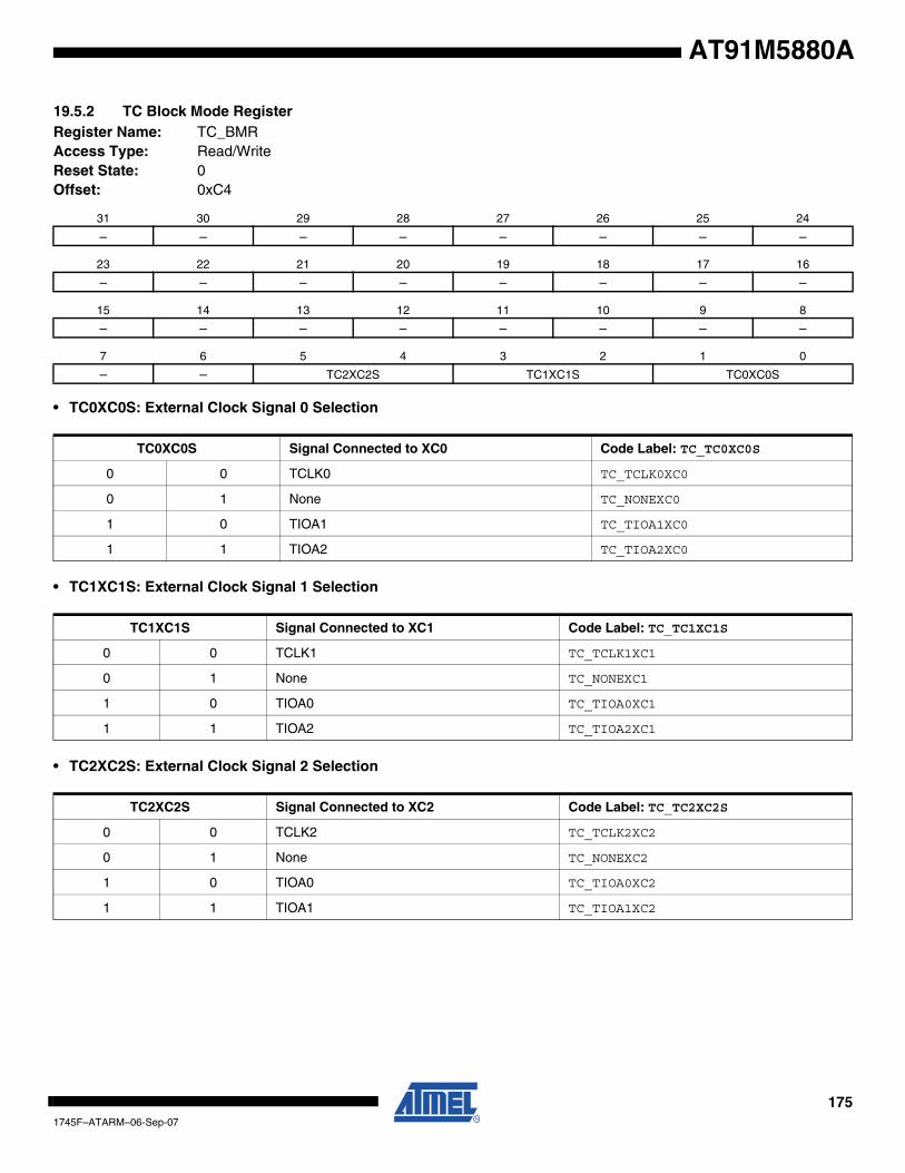
AT91M5880A
19.5.2 TC Block Mode Register Register Name: TC_BMRAccess Type: Read/WriteReset State: 0Offset: 0xC4
• TC0XC0S: External Clock Signal 0 Selection
• TC1XC1S: External Clock Signal 1 Selection
• TC2XC2S: External Clock Signal 2 Selection
31 30 29 28 27 26 25 24
– – – – – – – –
23 22 21 20 19 18 17 16
– – – – – – – –
15 14 13 12 11 10 9 8
– – – – – – – –
7 6 5 4 3 2 1 0
– – TC2XC2S TC1XC1S TC0XC0S
TC0XC0S Signal Connected to XC0 Code Label: TC_TC0XC0S
0 0 TCLK0 TC_TCLK0XC0
0 1 None TC_NONEXC0
1 0 TIOA1 TC_TIOA1XC0
1 1 TIOA2 TC_TIOA2XC0
TC1XC1S Signal Connected to XC1 Code Label: TC_TC1XC1S
0 0 TCLK1 TC_TCLK1XC1
0 1 None TC_NONEXC1
1 0 TIOA0 TC_TIOA0XC1
1 1 TIOA2 TC_TIOA2XC1
TC2XC2S Signal Connected to XC2 Code Label: TC_TC2XC2S
0 0 TCLK2 TC_TCLK2XC2
0 1 None TC_NONEXC2
1 0 TIOA0 TC_TIOA0XC2
1 1 TIOA1 TC_TIOA1XC2
1751745F–ATARM–06-Sep-07

19.5.3 TC Channel Control Register Register Name: TC_CCRAccess Type: Write-only Offset: 0x00
• CLKEN: Counter Clock Enable Command (Code Label TC_CLKEN)0 = No effect.
1 = Enables the clock if CLKDIS is not 1.
• CLKDIS: Counter Clock Disable Command (Code Label TC_CLKDIS)0 = No effect.
1 = Disables the clock.
• SWTRG: Software Trigger Command (Code Label TC_SWTRG)0 = No effect.
1 = A software trigger is performed: the counter is reset and clock is started.
31 30 29 28 27 26 25 24
– – – – – – – –
23 22 21 20 19 18 17 16
– – – – – – – –
15 14 13 12 11 10 9 8
– – – – – – – –
7 6 5 4 3 2 1 0
– – – – – SWTRG CLKDIS CLKEN
1761745F–ATARM–06-Sep-07
AT91M5880A

AT91M5880A
19.5.4 TC Channel Mode Register: Capture ModeRegister Name: TC_CMRAccess Type: Read/WriteReset State: 0Offset: 0x04
• TCCLKS: Clock Selection
• CLKI: Clock Invert (Code Label TC_CLKI)0 = Counter is incremented on rising edge of the clock.
1 = Counter is incremented on falling edge of the clock.
• BURST: Burst Signal Selection
• LDBSTOP: Counter Clock Stopped with RB Loading (Code Label TC_LDBSTOP)0 = Counter clock is not stopped when RB loading occurs.
1 = Counter clock is stopped when RB loading occurs.
31 30 29 28 27 26 25 24
– – – – – – – –
23 22 21 20 19 18 17 16
– – – – LDRB LDRA
15 14 13 12 11 10 9 8
WAVE=0 CPCTRG – – – ABETRG ETRGEDG
7 6 5 4 3 2 1 0
LDBDIS LDBSTOP BURST CLKI TCCLKS
TCCLKS Clock Selected Code Label: TC_CLKS
0 0 0 MCK/2 TC_CLKS_MCK2
0 0 1 MCK/8 TC_CLKS_MCK8
0 1 0 MCK/32 TC_CLKS_MCK32
0 1 1 MCK/128 TC_CLKS_MCK128
1 0 0 MCK/1024 TC_CLKS_MCK1024
1 0 1 XC0 TC_CLKS_XC0
1 1 0 XC1 TC_CLKS_XC1
1 1 1 XC2 TC_CLKS_XC2
BURST Selected BURST Code Label: TC_BURST
0 0 The clock is not gated by an external signal. TC_BURST_NONE
0 1 XC0 is ANDed with the selected clock. TC_BURST_XC0
1 0 XC1 is ANDed with the selected clock. TC_BURST_XC1
1 1 XC2 is ANDed with the selected clock. TC_BURST_XC2
1771745F–ATARM–06-Sep-07
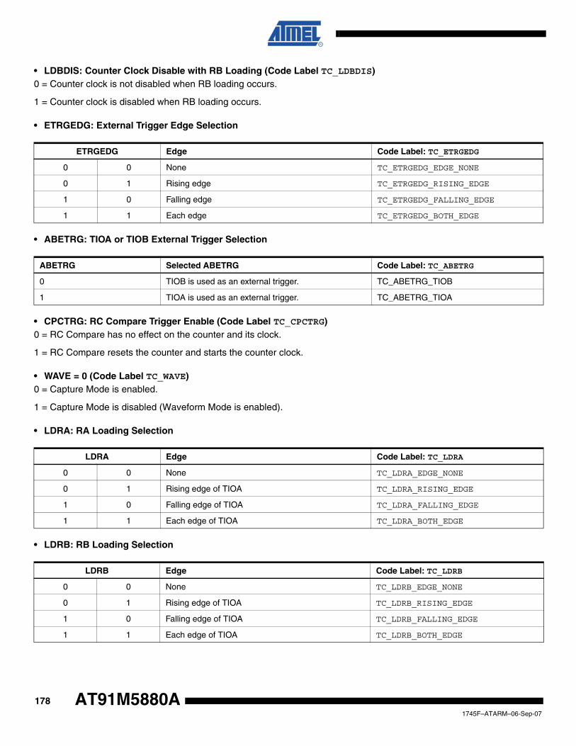
• LDBDIS: Counter Clock Disable with RB Loading (Code Label TC_LDBDIS)0 = Counter clock is not disabled when RB loading occurs.
1 = Counter clock is disabled when RB loading occurs.
• ETRGEDG: External Trigger Edge Selection
• ABETRG: TIOA or TIOB External Trigger Selection
• CPCTRG: RC Compare Trigger Enable (Code Label TC_CPCTRG)0 = RC Compare has no effect on the counter and its clock.
1 = RC Compare resets the counter and starts the counter clock.
• WAVE = 0 (Code Label TC_WAVE)0 = Capture Mode is enabled.
1 = Capture Mode is disabled (Waveform Mode is enabled).
• LDRA: RA Loading Selection
• LDRB: RB Loading Selection
ETRGEDG Edge Code Label: TC_ETRGEDG
0 0 None TC_ETRGEDG_EDGE_NONE
0 1 Rising edge TC_ETRGEDG_RISING_EDGE
1 0 Falling edge TC_ETRGEDG_FALLING_EDGE
1 1 Each edge TC_ETRGEDG_BOTH_EDGE
ABETRG Selected ABETRG Code Label: TC_ABETRG
0 TIOB is used as an external trigger. TC_ABETRG_TIOB
1 TIOA is used as an external trigger. TC_ABETRG_TIOA
LDRA Edge Code Label: TC_LDRA
0 0 None TC_LDRA_EDGE_NONE
0 1 Rising edge of TIOA TC_LDRA_RISING_EDGE
1 0 Falling edge of TIOA TC_LDRA_FALLING_EDGE
1 1 Each edge of TIOA TC_LDRA_BOTH_EDGE
LDRB Edge Code Label: TC_LDRB
0 0 None TC_LDRB_EDGE_NONE
0 1 Rising edge of TIOA TC_LDRB_RISING_EDGE
1 0 Falling edge of TIOA TC_LDRB_FALLING_EDGE
1 1 Each edge of TIOA TC_LDRB_BOTH_EDGE
1781745F–ATARM–06-Sep-07
AT91M5880A

AT91M5880A
19.5.5 TC Channel Mode Register: Waveform ModeRegister Name: TC_CMRAccess Type: Read/WriteReset State: 0Offset: 0x4
• TCCLKS: Clock Selection
• CLKI: Clock Invert (Code Label TC_CLKI)0 = Counter is incremented on rising edge of the clock.
1 = Counter is incremented on falling edge of the clock.
• BURST: Burst Signal Selection
• CPCSTOP: Counter Clock Stopped with RC Compare (Code Label TC_CPCSTOP)0 = Counter clock is not stopped when counter reaches RC.
1 = Counter clock is stopped when counter reaches RC.
31 30 29 28 27 26 25 24
BSWTRG BEEVT BCPC BCPB
23 22 21 20 19 18 17 16
ASWTRG AEEVT ACPC ACPA
15 14 13 12 11 10 9 8
WAVE=1 CPCTRG – ENETRG EEVT EEVTEDG
7 6 5 4 3 2 1 0
CPCDIS CPCSTOP BURST CLKI TCCLKS
TCCLKS Clock Selected Code Label: TC_CLKS
0 0 0 MCK/2 TC_CLKS_MCK2
0 0 1 MCK/8 TC_CLKS_MCK8
0 1 0 MCK/32 TC_CLKS_MCK32
0 1 1 MCK/128 TC_CLKS_MCK128
1 0 0 MCK/1024 TC_CLKS_MCK1024
1 0 1 XC0 TC_CLKS_XC0
1 1 0 XC1 TC_CLKS_XC1
1 1 1 XC2 TC_CLKS_XC2
BURST Selected BURST Code Label: TC_BURST
0 0 The clock is not gated by an external signal. TC_BURST_NONE
0 1 XC0 is ANDed with the selected clock. TC_BURST_XC0
1 0 XC1 is ANDed with the selected clock. TC_BURST_XC1
1 1 XC2 is ANDed with the selected clock. TC_BURST_XC2
1791745F–ATARM–06-Sep-07

• CPCDIS: Counter Clock Disable with RC Compare (Code Label TC_CPCDIS)0 = Counter clock is not disabled when counter reaches RC.
1 = Counter clock is disabled when counter reaches RC.
• EEVTEDG: External Event Edge Selection
• EEVT: External Event Selection
Note: If TIOB is chosen as the external event signal, it is configured as an input and no longer generates waveforms.
• ENETRG: External Event Trigger Enable (Code Label TC_ENETRG)0 = The external event has no effect on the counter and its clock. In this case, the selected external event only controls theTIOA output.
1 = The external event resets the counter and starts the counter clock.
• CPCTRG: RC Compare Trigger Enable (Code Label TC_CPCTRG)0 = RC Compare has no effect on the counter and its clock.
1 = RC Compare resets the counter and starts the counter clock.
• WAVE = 1 (Code Label TC_WAVE)0 = Waveform Mode is disabled (Capture Mode is enabled).
1 = Waveform Mode is enabled.
• ACPA: RA Compare Effect on TIOA
EEVTEDG Edge Code Label: TC_EEVTEDG
0 0 None TC_EEVTEDG_EDGE_NONE
0 1 Rising edge TC_EEVTEDG_RISING_EDGE
1 0 Falling edge TC_EEVTEDG_FALLING_EDGE
1 1 Each edge TC_EEVTEDG_BOTH_EDGE
EEVTSignal Selected as
External Event TIOB Direction Code Label: TC_EEVT
0 0 TIOB Input(1) TC_EEVT_TIOB
0 1 XC0 Output TC_EEVT_XC0
1 0 XC1 Output TC_EEVT_XC1
1 1 XC2 Output TC_EEVT_XC2
ACPA Effect Code Label: TC_ACPA
0 0 None TC_ACPA_OUTPUT_NONE
0 1 Set TC_ACPA_SET_OUTPUT
1 0 Clear TC_ACPA_CLEAR_OUTPUT
1 1 Toggle TC_ACPA_TOGGLE_OUTPUT
1801745F–ATARM–06-Sep-07
AT91M5880A

AT91M5880A
• ACPC: RC Compare Effect on TIOA
• AEEVT: External Event Effect on TIOA
• ASWTRG: Software Trigger Effect on TIOA
• BCPB: RB Compare Effect on TIOB
• BCPC: RC Compare Effect on TIOB
ACPC Effect Code Label: TC_ACPC
0 0 None TC_ACPC_OUTPUT_NONE
0 1 Set TC_ACPC_SET_OUTPUT
1 0 Clear TC_ACPC_CLEAR_OUTPUT
1 1 Toggle TC_ACPC_TOGGLE_OUTPUT
AEEVT Effect Code Label: TC_AEEVT
0 0 None TC_AEEVT_OUTPUT_NONE
0 1 Set TC_AEEVT_SET_OUTPUT
1 0 Clear TC_AEEVT_CLEAR_OUTPUT
1 1 Toggle TC_AEEVT_TOGGLE_OUTPUT
ASWTRG Effect Code Label: TC_ASWTRG
0 0 None TC_ASWTRG_OUTPUT_NONE
0 1 Set TC_ASWTRG_SET_OUTPUT
1 0 Clear TC_ASWTRG_CLEAR_OUTPUT
1 1 Toggle TC_ASWTRG_TOGGLE_OUTPUT
BCPB Effect Code Label: TC_BCPB
0 0 None TC_BCPB_OUTPUT_NONE
0 1 Set TC_BCPB_SET_OUTPUT
1 0 Clear TC_BCPB_CLEAR_OUTPUT
1 1 Toggle TC_BCPB_TOGGLE_OUTPUT
BCPC Effect Code Label: TC_BCPC
0 0 None TC_BCPC_OUTPUT_NONE
0 1 Set TC_BCPC_SET_OUTPUT
1 0 Clear TC_BCPC_CLEAR_OUTPUT
1 1 Toggle TC_BCPC_TOGGLE_OUTPUT
1811745F–ATARM–06-Sep-07

• BEEVT: External Event Effect on TIOB
• BSWTRG: Software Trigger Effect on TIOB
BEEVT Effect Code Label: TC_BEEVT
0 0 None TC_BEEVT_OUTPUT_NONE
0 1 Set TC_BEEVT_SET_OUTPUT
1 0 Clear TC_BEEVT_CLEAR_OUTPUT
1 1 Toggle TC_BEEVT_TOGGLE_OUTPUT
BSWTRG Effect Code Label: TC_BSWTRG
0 0 None TC_BSWTRG_OUTPUT_NONE
0 1 Set TC_BSWTRG_SET_OUTPUT
1 0 Clear TC_BSWTRG_CLEAR_OUTPUT
1 1 Toggle TC_BSWTRG_TOGGLE_OUTPUT
1821745F–ATARM–06-Sep-07
AT91M5880A

AT91M5880A
19.5.6 TC Counter Value Register Register Name: TC_CVRAccess Type: Read-onlyReset State: 0Offset: 0x10
• CV: Counter Value (Code Label TC_CV)CV contains the counter value in real-time.
19.5.7 TC Register ARegister Name: TC_RAAccess Type: Read-only if WAVE = 0, Read/Write if WAVE = 1Reset State: 0Offset: 0x14
• RA: Register A (Code Label TC_RA)RA contains the Register A value in real-time.
31 30 29 28 27 26 25 24
– – – – – – – –
23 22 21 20 19 18 17 16
– – – – – – – –
15 14 13 12 11 10 9 8
CV
7 6 5 4 3 2 1 0
CV
31 30 29 28 27 26 25 24
– – – – – – – –
23 22 21 20 19 18 17 16
– – – – – – – –
15 14 13 12 11 10 9 8
RA
7 6 5 4 3 2 1 0
RA
1831745F–ATARM–06-Sep-07

19.5.8 TC Register BRegister Name: TC_RBAccess Type: Read-only if WAVE = 0, Read/Write if WAVE = 1Reset State: 0Offset: 0x18
• RB: Register B (Code Label TC_RB)RB contains the Register B value in real-time.
19.5.9 TC Register CRegister Name: TC_RCAccess Type: Read/WriteReset State: 0Offset: 0x1C
• RC: Register C (Code Label TC_RC)RC contains the Register C value in real-time.
31 30 29 28 27 26 25 24
– – – – – – – –
23 22 21 20 19 18 17 16
– – – – – – – –
15 14 13 12 11 10 9 8
RB
7 6 5 4 3 2 1 0
RB
31 30 29 28 27 26 25 24
– – – – – – – –
23 22 21 20 19 18 17 16
– – – – – – – –
15 14 13 12 11 10 9 8
RC
7 6 5 4 3 2 1 0
RC
1841745F–ATARM–06-Sep-07
AT91M5880A

AT91M5880A
19.5.10 TC Status Register Register Name: TC_SRAccess Type: Read/WriteOffset: 0x20
• COVFS: Counter Overflow Status (Code Label TC_COVFS)0 = No counter overflow has occurred since the last read of the Status Register.
1 = A counter overflow has occurred since the last read of the Status Register.
• LOVRS: Load Overrun Status (Code Label TC_LOVRS)0 = Load overrun has not occurred since the last read of the Status Register or WAVE = 1.
1 = RA or RB have been loaded at least twice without any read of the corresponding register since the last read of the Sta-tus Register, if WAVE = 0.
• CPAS: RA Compare Status (Code Label TC_CPAS)0 = RA Compare has not occurred since the last read of the Status Register or WAVE = 0.
1 = RA Compare has occurred since the last read of the Status Register, if WAVE = 1.
• CPBS: RB Compare Status (Code Label TC_CPBS)0 = RB Compare has not occurred since the last read of the Status Register or WAVE = 0.
1 = RB Compare has occurred since the last read of the Status Register, if WAVE = 1.
• CPCS: RC Compare Status (Code Label TC_CPCS)0 = RC Compare has not occurred since the last read of the Status Register.
1 = RC Compare has occurred since the last read of the Status Register.
• LDRAS: RA Loading Status (Code Label TC_LDRAS)0 = RA Load has not occurred since the last read of the Status Register or WAVE = 1.
1 = RA Load has occurred since the last read of the Status Register, if WAVE = 0.
• LDRBS: RB Loading Status (Code Label TC_LDRBS)0 = RB Load has not occurred since the last read of the Status Register or WAVE = 1.
1 = RB Load has occurred since the last read of the Status Register, if WAVE = 0.
• ETRGS: External Trigger Status (Code Label TC_ETRGS)0 = External trigger has not occurred since the last read of the Status Register.
1 = External trigger has occurred since the last read of the Status Register.
31 30 29 28 27 26 25 24
– – – – – – – –
23 22 21 20 19 18 17 16
– – – – – MTIOB MTIOA CLKSTA
15 14 13 12 11 10 9 8
– – – – – – – –
7 6 5 4 3 2 1 0
ETRGS LDRBS LDRAS CPCS CPBS CPAS LOVRS COVFS
1851745F–ATARM–06-Sep-07

• CLKSTA: Clock Enabling Status (Code Label TC_CLKSTA)0 = Clock is disabled.
1 = Clock is enabled.
• MTIOA: TIOA Mirror (Code Label TC_MTIOA)0 = TIOA is low. If WAVE = 0, this means that TIOA pin is low. If WAVE = 1, this means that TIOA is driven low.
1 = TIOA is high. If WAVE = 0, this means that TIOA pin is high. If WAVE = 1, this means that TIOA is driven high.
• MTIOB: TIOB Mirror (Code Label TC_MTIOB)0 = TIOB is low. If WAVE = 0, this means that TIOB pin is low. If WAVE = 1, this means that TIOB is driven low.
1 = TIOB is high. If WAVE = 0, this means that TIOB pin is high. If WAVE = 1, this means that TIOB is driven high.
1861745F–ATARM–06-Sep-07
AT91M5880A

AT91M5880A
19.5.11 TC Interrupt Enable Register Register Name: TC_IERAccess Type: Write-onlyOffset: 0x24
• COVFS: Counter Overflow (Code Label TC_COVFS)0 = No effect.
1 = Enables the Counter Overflow Interrupt.
• LOVRS: Load Overrun (Code Label TC_LOVRS)0 = No effect.
1: Enables the Load Overrun Interrupt.
• CPAS: RA Compare (Code Label TC_CPAS)0 = No effect.
1 = Enables the RA Compare Interrupt.
• CPBS: RB Compare (Code Label TC_CPBS)0 = No effect.
1 = Enables the RB Compare Interrupt.
• CPCS: RC Compare (Code Label TC_CPCS)0 = No effect.
1 = Enables the RC Compare Interrupt.
• LDRAS: RA Loading (Code Label TC_LDRAS)0 = No effect.
1 = Enables the RA Load Interrupt.
• LDRBS: RB Loading (Code Label TC_LDRBS)0 = No effect.
1 = Enables the RB Load Interrupt.
• ETRGS: External Trigger (Code Label TC_ETRGS)0 = No effect.
1 = Enables the External Trigger Interrupt.
31 30 29 28 27 26 25 24
– – – – – – – –
23 22 21 20 19 18 17 16
– – – – – – – –
15 14 13 12 11 10 9 8
– – – – – – – –
7 6 5 4 3 2 1 0
ETRGS LDRBS LDRAS CPCS CPBS CPAS LOVRS COVFS
1871745F–ATARM–06-Sep-07

19.5.12 TC Interrupt Disable Register Register Name: TC_IDRAccess Type: Write-onlyOffset: 0x28
• COVFS: Counter Overflow (Code Label TC_COVFS)0 = No effect.
1 = Disables the Counter Overflow Interrupt.
• LOVRS: Load Overrun (Code Label TC_LOVRS)0 = No effect.
1 = Disables the Load Overrun Interrupt (if WAVE = 0).
• CPAS: RA Compare (Code Label TC_CPAS)0 = No effect.
1 = Disables the RA Compare Interrupt (if WAVE = 1).
• CPBS: RB Compare (Code Label TC_CPBS)0 = No effect.
1 = Disables the RB Compare Interrupt (if WAVE = 1).
• CPCS: RC Compare (Code Label TC_CPCS)0 = No effect.
1 = Disables the RC Compare Interrupt.
• LDRAS: RA Loading (Code Label TC_LDRAS)0 = No effect.
1 = Disables the RA Load Interrupt (if WAVE = 0).
• LDRBS: RB Loading (Code Label TC_LDRBS)0 = No effect.
1 = Disables the RB Load Interrupt (if WAVE = 0).
• ETRGS: External Trigger (Code Label TC_ETRGS)0 = No effect.
1 = Disables the External Trigger Interrupt.
31 30 29 28 27 26 25 24
– – – – – – – –
23 22 21 20 19 18 17 16
– – – – – – – –
15 14 13 12 11 10 9 8
– – – – – – – –
7 6 5 4 3 2 1 0
ETRGS LDRBS LDRAS CPCS CPBS CPAS LOVRS COVFS
1881745F–ATARM–06-Sep-07
AT91M5880A

AT91M5880A
19.5.13 TC Interrupt Mask Register Register Name: TC_IMRAccess Type: Read-onlyReset State: 0Offset: 0x2C
• COVFS: Counter Overflow (Code Label TC_COVFS)0 = The Counter Overflow Interrupt is disabled.
1 = The Counter Overflow Interrupt is enabled.
• LOVRS: Load Overrun (Code Label TC_LOVRS)0 = The Load Overrun Interrupt is disabled.
1 = The Load Overrun Interrupt is enabled.
• CPAS: RA Compare (Code Label TC_CPAS)0 = The RA Compare Interrupt is disabled.
1 = The RA Compare Interrupt is enabled.
• CPBS: RB Compare (Code Label TC_CPBS)0 = The RB Compare Interrupt is disabled.
1 = The RB Compare Interrupt is enabled.
• CPCS: RC Compare (Code Label TC_CPCS)0 = The RC Compare Interrupt is disabled.
1 = The RC Compare Interrupt is enabled.
• LDRAS: RA Loading (Code Label TC_LDRAS)0 = The Load RA Interrupt is disabled.
1 = The Load RA Interrupt is enabled.
• LDRBS: RB Loading (Code Label TC_LDRBS)0 = The Load RB Interrupt is disabled.
1 = The Load RB Interrupt is enabled.
• ETRGS: External Trigger (Code Label TC_ETRGS)0 = The External Trigger Interrupt is disabled.
1 = The External Trigger Interrupt is enabled.
31 30 29 28 27 26 25 24
– – – – – – – –
23 22 21 20 19 18 17 16
– – – – – – – –
15 14 13 12 11 10 9 8
– – – – – – – –
7 6 5 4 3 2 1 0
ETRGS LDRBS LDRAS CPCS CPBS CPAS LOVRS COVFS
1891745F–ATARM–06-Sep-07

20. SPI: Serial Peripheral InterfaceThe AT91M55800A includes an SPI which provides communication with external devices inmaster or slave mode.
The SPI has four external chip selects which can be connected to up to 15 devices. The datalength is programmable, from 8- to 16-bit.
As for the USART, a 2-channel PDC can be used to move data between memory and the SPIwithout CPU intervention.
20.1 Pin DescriptionSeven pins are associated with the SPI Interface. When not needed for the SPI function, each ofthese pins can be configured as a PIO.
Support for an external master is provided by the PIO Controller Multi-driver option. To configurean SPI pin as open-drain to support external drivers, set the corresponding bits in thePIO_MDSR register.
An input filter can be enabled on the SPI input pins by setting the corresponding bits in thePIO_IFSR.
The NPCS0/NSS pin can function as a peripheral chip select output or slave select input. Referto Table 20-1 for a description of the SPI pins.
Figure 20-1. SPI Block Diagram
Serial Peripheral Interface
APB
MCK
MCK/32
Parallel IOController
MISO
MOSI
SPCK
NPCS0/NSS
NPCS1
NPCS2
NPCS3
MISO
MOSI
SPCK
NPCS0/NSS
NPCS1
NPCS2
NPCS3INT
Advanced Interrupt Controller
1901745F–ATARM–06-Sep-07
AT91M5880A

AT91M5880A
Notes: 1. After a hardware reset, the SPI clock is disabled by default. The user must configure the Power Management Controller before any access to the User Interface of the SPI.
2. After a hardware reset, the SPI pins are deselected by default (see Section 16. “PIO: Parallel I/O Controller” on page 113). The user must configure the PIO Controller to enable the corresponding pins for their SPI function. NPCS0/NSS must be configured as open drain in the Parallel I/O Controller for multi-master operation.
20.2 Master ModeIn Master Mode, the SPI controls data transfers to and from the slave(s) connected to the SPIbus. The SPI drives the chip select(s) to the slave(s) and the serial clock (SPCK). After enablingthe SPI, a data transfer begins when the ARM core writes to the SP_TDR (Transmit DataRegister).
Transmit and Receive buffers maintain the data flow at a constant rate with a reduced require-ment for high priority interrupt servicing. When new data is available in the SP_TDR (TransmitData Register) the SPI continues to transfer data. If the SP_RDR (Receive Data Register) hasnot been read before new data is received, the Overrun Error (OVRES) flag is set.
The delay between the activation of the chip select and the start of the data transfer (DLYBS) aswell as the delay between each data transfer (DLYBCT) can be programmed for each of the fourexternal chip selects. All data transfer characteristics including the two timing values are pro-grammed in registers SP_CSR0 to SP_CSR3 (Chip Select Registers). See Table 20-2.
In master mode the peripheral selection can be defined in two different ways:
• Fixed Peripheral Select: SPI exchanges data with only one peripheral
• Variable Peripheral Select: Data can be exchanged with more than one peripheral
Figures 20-2 and 20-3 show the operation of the SPI in Master Mode. For details concerning theflag and control bits in these diagrams, see the tables in the Programmer’s Model, starting onpage 198.
20.2.1 Fixed Peripheral SelectThis mode is ideal for transferring memory blocks without the extra overhead in the transmit dataregister to determine the peripheral.
Fixed Peripheral Select is activated by setting bit PS to zero in SP_MR (Mode Register). Theperipheral is defined by the PCS field, also in SP_MR.
This option is only available when the SPI is programmed in master mode.
Table 20-1. SPI Pins
Pin Name Mnemonic Mode Function
Master In Slave Out MISO MasterSlave
Serial data input to SPISerial data output from SPI
Master Out Slave In MOSI MasterSlave
Serial data output from SPISerial data input to SPI
Serial Clock SPCK MasterSlave
Clock output from SPIClock input to SPI
Peripheral Chip Selects NPCS[3:1] Master Select peripherals
Peripheral Chip Select/Slave Select
NPCS0/NSS
MasterMasterSlave
Output: Selects peripheralInput: low causes mode faultInput: chip select for SPI
1911745F–ATARM–06-Sep-07
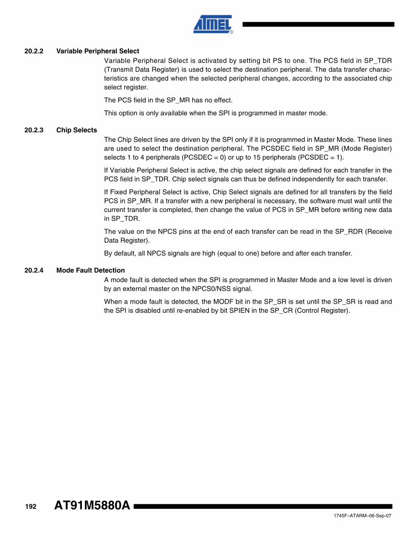
20.2.2 Variable Peripheral SelectVariable Peripheral Select is activated by setting bit PS to one. The PCS field in SP_TDR(Transmit Data Register) is used to select the destination peripheral. The data transfer charac-teristics are changed when the selected peripheral changes, according to the associated chipselect register.
The PCS field in the SP_MR has no effect.
This option is only available when the SPI is programmed in master mode.
20.2.3 Chip SelectsThe Chip Select lines are driven by the SPI only if it is programmed in Master Mode. These linesare used to select the destination peripheral. The PCSDEC field in SP_MR (Mode Register)selects 1 to 4 peripherals (PCSDEC = 0) or up to 15 peripherals (PCSDEC = 1).
If Variable Peripheral Select is active, the chip select signals are defined for each transfer in thePCS field in SP_TDR. Chip select signals can thus be defined independently for each transfer.
If Fixed Peripheral Select is active, Chip Select signals are defined for all transfers by the fieldPCS in SP_MR. If a transfer with a new peripheral is necessary, the software must wait until thecurrent transfer is completed, then change the value of PCS in SP_MR before writing new datain SP_TDR.
The value on the NPCS pins at the end of each transfer can be read in the SP_RDR (ReceiveData Register).
By default, all NPCS signals are high (equal to one) before and after each transfer.
20.2.4 Mode Fault DetectionA mode fault is detected when the SPI is programmed in Master Mode and a low level is drivenby an external master on the NPCS0/NSS signal.
When a mode fault is detected, the MODF bit in the SP_SR is set until the SP_SR is read andthe SPI is disabled until re-enabled by bit SPIEN in the SP_CR (Control Register).
1921745F–ATARM–06-Sep-07
AT91M5880A

AT91M5880A
Figure 20-2. Functional Flow Diagram in Master Mode
SPI Enable
TDRE
PS
1
0
0
1
1
1
0
Same Peripheral
New Peripheral
NPCS = SP_TDR(PCS) NPCS = SP_MR(PCS)
Delay DLYBS
Serializer = SP_TDR(TD)TDRE = 1
Data Transfer
SP_RDR(RD) = SerializerRDRF = 1
TDRE
PS
NPCS = 0xF
Delay DLYBCS
SP_TDR(PCS)
NPCS = 0xF
Delay DLYBCS
NPCS = SP_TDR(PCS)
Fixed Peripheral
Variable Peripheral
Fixed Peripheral
Variable Peripheral
Delay DLYBCT
0
1931745F–ATARM–06-Sep-07

Figure 20-3. SPI in Master Mode
0
1
SP_MR(MCK32)
MCK
MCK/32
SPCK Clock Generator
SP_CSRx[15:0]
S
R
Q
MODF
TDRE
RDRF
OVRE
SPIENS
0
1
SP_MR(PS)
PCSSP_RDR
SerializerMISO
SP_MR(PCS)
SPIDIS SPIEN
SP_MR(MSTR)
SP_IERSP_IDRSP_IMR
SP_SR
MOSI
NPCS3
NPCS2
NPCS1
NPCS0
LSB MSB
SPCK
SPIRQ
SPI Master Clock
RD
PCSSP_TDR
TD
1941745F–ATARM–06-Sep-07
AT91M5880A

AT91M5880A
20.3 Slave ModeIn Slave Mode, the SPI waits for NSS to go active low before receiving the serial clock from anexternal master.
In slave mode CPOL, NCPHA and BITS fields of SP_CSR0 are used to define the transfer char-acteristics. The other Chip Select Registers are not used in slave mode.
Figure 2. SPI in Slave Mode
S
R
Q
TDRE
RDRF
OVRE
SPIENS
Serializer
SCK
SPIDIS SPIEN
SP_IERSP_IDRSP_IMR
SP_SR
MISOLSB MSB
NSS
MOSI
SPIRQ
SP_RDRRD
SP_TDRTD
1951745F–ATARM–06-Sep-07

20.4 Data TransferThe following waveforms show examples of data transfers.
Figure 20-4. SPI Transfer Format (NCPHA equals One, 8 bits per transfer)
Figure 20-5. SPI Transfer Format (NCPHA equals Zero, 8 bits per transfer)
SPCK(CPOL=0)
SPCK(CPOL=1)
1 2 3 4 5 6 7
MOSI(from master)
MISO(from slave)
NSS (to slave)
SPCK cycle (for reference) 8
MSB
MSB
LSB
LSB
6
6
6
5
5
4
4
3
3
2
2
1
1 X
SPCK(CPOL=0)
SPCK(CPOL=1)
1 2 3 4 5 6 7
MOSI(from master)
MISO(from slave)
NSS (to slave)
SPCK cycle (for reference) 8
MSB
MSB
LSB
LSB
6
6
6
5
5
4
4
3
3
2
2
1
1X
1961745F–ATARM–06-Sep-07
AT91M5880A

AT91M5880A
Figure 20-6. Programmable Delays (DLYBCS, DLYBS and DLYBCT)
20.5 Clock GenerationIn master mode the SPI Master Clock is either MCK or MCK/32, as defined by the MCK32 fieldof SP_MR. The SPI baud rate clock is generated by dividing the SPI Master Clock by a valuebetween 4 and 510. The divisor is defined in the SCBR field in each Chip Select Register. Thetransfer speed can thus be defined independently for each chip select signal.
CPOL and NCPHA in the Chip Select Registers define the clock/data relationship between mas-ter and slave devices. CPOL defines the inactive value of the SPCK. NCPHA defines whichedge causes data to change and which edge causes data to be captured.
In Slave Mode, the input clock low and high pulse duration must strictly be longer than two sys-tem clock (MCK) periods.
20.6 Peripheral Data ControllerThe SPI is closely connected to two Peripheral Data Controller channels. One is dedicated tothe receiver. The other is dedicated to the transmitter.
The PDC channel is programmed using SP_TPR (Transmit Pointer) and SP_TCR (TransmitCounter) for the transmitter and SP_RPR (Receive Pointer) and SP_RCR (Receive Counter) forthe receiver. The status of the PDC is given in SP_SR by the SPENDTX bit for the transmitterand by the SPENDRX bit for the receiver.
The pointer registers (SP_TPR and SP_RPR) are used to store the address of the transmit orreceive buffers. The counter registers (SP_TCR and SP_RCR) are used to store the size ofthese buffers.
The receiver data transfer is triggered by the RDRF bit and the transmitter data transfer is trig-gered by TDRE. When a transfer is performed, the counter is decremented and the pointer isincremented. When the counter reaches 0, the status bit is set (SPENDRX for the receiver,SPENDTX for the transmitter in SP_SR) and can be programmed to generate an interrupt. Whilethe counter is at zero, the status bit is asserted and transfers are disabled.
Chip Select 1
Chip Select 2
SPCK Output
DLYBCS DLYBS DLYBCT
Change peripheralNo change of peripheral
DLYBCT
1971745F–ATARM–06-Sep-07

20.7 SPI User InterfaceSPI Base Address: 0xFFFBC000 (Code Label SPI_BASE)
Table 20-2. Register Mapping
Offset Register Name Access Reset
0x00 Control Register SP_CR Write-only –
0x04 Mode Register SP_MR Read/Write 0
0x08 Receive Data Register SP_RDR Read-only 0
0x0C Transmit Data Register SP_TDR Write-only –
0x10 Status Register SP_SR Read-only 0
0x14 Interrupt Enable Register SP_IER Write-only –
0x18 Interrupt Disable Register SP_IDR Write-only –
0x1C Interrupt Mask Register SP_IMR Read-only 0
0x20 Receive Pointer Register SP_RPR Read/Write 0
0x24 Receive Counter Register SP_RCR Read/Write 0
0x28 Transmit Pointer Register SP_TPR Read/Write 0
0x2C Transmit Counter Register SP_TCR Read/Write 0
0x30 Chip Select Register 0 SP_CSR0 Read/Write 0
0x34 Chip Select Register 1 SP_CSR1 Read/Write 0
0x38 Chip Select Register 2 SP_CSR2 Read/Write 0
0x3C Chip Select Register 3 SP_CSR3 Read/Write 0
1981745F–ATARM–06-Sep-07
AT91M5880A

AT91M5880A
20.7.1 SPI Control Register Register Name: SP_CRAccess Type: Write-onlyOffset: 0x00
• SPIEN: SPI Enable (Code Label SP_SPIEN)0 = No effect.
1 = Enables the SPI to transfer and receive data.
• SPIDIS: SPI Disable (Code Label SP_SPIDIS)0 = No effect.
1 = Disables the SPI.
All pins are set in input mode and no data is received or transmitted.
If a transfer is in progress, the transfer is finished before the SPI is disabled.
If both SPIEN and SPIDIS are equal to one when the control register is written, the SPI is disabled.
• SWRST: SPI Software reset (Code Label SP_SWRST)0 = No effect.
1 = Resets the SPI.
A software triggered hardware reset of the SPI interface is performed.
31 30 29 28 27 26 25 24
– – – – – – – –
23 22 21 20 19 18 17 16
– – – – – – – –
15 14 13 12 11 10 9 8
– – – – – – – –
7 6 5 4 3 2 1 0
SWRST – – – – – SPIDIS SPIEN
1991745F–ATARM–06-Sep-07
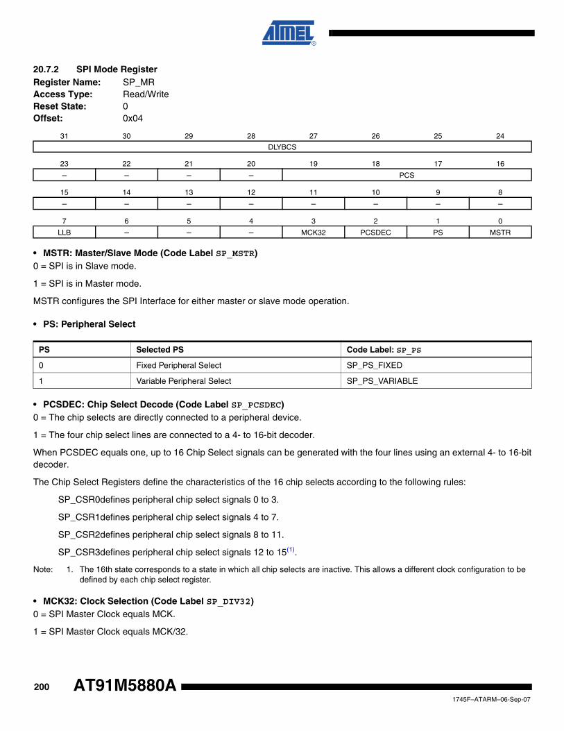
20.7.2 SPI Mode RegisterRegister Name: SP_MRAccess Type: Read/WriteReset State: 0Offset: 0x04
• MSTR: Master/Slave Mode (Code Label SP_MSTR)0 = SPI is in Slave mode.
1 = SPI is in Master mode.
MSTR configures the SPI Interface for either master or slave mode operation.
• PS: Peripheral Select
• PCSDEC: Chip Select Decode (Code Label SP_PCSDEC)0 = The chip selects are directly connected to a peripheral device.
1 = The four chip select lines are connected to a 4- to 16-bit decoder.
When PCSDEC equals one, up to 16 Chip Select signals can be generated with the four lines using an external 4- to 16-bitdecoder.
The Chip Select Registers define the characteristics of the 16 chip selects according to the following rules:
SP_CSR0defines peripheral chip select signals 0 to 3.
SP_CSR1defines peripheral chip select signals 4 to 7.
SP_CSR2defines peripheral chip select signals 8 to 11.
SP_CSR3defines peripheral chip select signals 12 to 15(1).
Note: 1. The 16th state corresponds to a state in which all chip selects are inactive. This allows a different clock configuration to be defined by each chip select register.
• MCK32: Clock Selection (Code Label SP_DIV32)0 = SPI Master Clock equals MCK.
1 = SPI Master Clock equals MCK/32.
31 30 29 28 27 26 25 24
DLYBCS
23 22 21 20 19 18 17 16
– – – – PCS
15 14 13 12 11 10 9 8
– – – – – – – –
7 6 5 4 3 2 1 0
LLB – – – MCK32 PCSDEC PS MSTR
PS Selected PS Code Label: SP_PS
0 Fixed Peripheral Select SP_PS_FIXED
1 Variable Peripheral Select SP_PS_VARIABLE
2001745F–ATARM–06-Sep-07
AT91M5880A

AT91M5880A
• LLB: Local Loopback Enable (Code Label SP_LLB)0 = Local loopback path disabled.
1 = Local loopback path enabled.
LLB controls the local loopback on the data serializer for testing in master mode only.
• PCS: Peripheral Chip Select (Code Label SP_PCS)This field is only used if Fixed Peripheral Select is active (PS=0).
If PCSDEC=0:
PCS = xxx0NPCS[3:0] = 1110 (Code Label SP_PCS0)
PCS = xx01NPCS[3:0] = 1101 (Code Label SP_PCS1)
PCS = x011NPCS[3:0] = 1011 (Code Label SP_PCS2)
PCS = 0111NPCS[3:0] = 0111 (Code Label SP_PCS3)
PCS = 1111forbidden (no peripheral is selected)
(x = don’t care)
If PCSDEC=1:
NPCS[3:0] output signals = PCS.
• DLYBCS: Delay Between Chip Selects (Code Label SP_DLYBCS)This field defines the delay from NPCS inactive to the activation of another NPCS. The DLYBCS time guarantees non-over-lapping chip selects and solves bus contentions in case of peripherals having long data float times.
If DLYBCS is less than or equal to six, six SPI Master Clock periods will be inserted by default.
Otherwise, the following equation determines the delay:
Delay_ Between_Chip_Selects = DLYBCS * SPI_Master_Clock_period
2011745F–ATARM–06-Sep-07

20.7.3 SPI Receive Data RegisterRegister Name: SP_RDRAccess Type: Read-onlyReset State: 0Offset: 0x08
• RD: Receive Data (Code Label SP_RD)Data received by the SPI Interface is stored in this register right-justified. Unused bits read zero.
• PCS: Peripheral Chip Select StatusIn Master Mode only, these bits indicate the value on the NPCS pins at the end of a transfer. Otherwise, these bits readzero.
31 30 29 28 27 26 25 24
– – – – – – – –
23 22 21 20 19 18 17 16
– – – – PCS
15 14 13 12 11 10 9 8
RD
7 6 5 4 3 2 1 0
RD
2021745F–ATARM–06-Sep-07
AT91M5880A

AT91M5880A
20.7.4 SPI Transmit Data RegisterRegister Name: SP_TDRAccess Type: Write-onlyOffset: 0x0C
• TD: Transmit Data (Code Label SP_TD)Data which is to be transmitted by the SPI Interface is stored in this register. Information to be transmitted must be writtento the transmit data register in a right-justified format.
• PCS: Peripheral Chip SelectThis field is only used if Variable Peripheral Select is active (PS = 1) and if the SPI is in Master Mode.
If PCSDEC = 0:
PCS = xxx0NPCS[3:0] = 1110
PCS = xx01NPCS[3:0] = 1101
PCS = x011NPCS[3:0] = 1011
PCS = 0111NPCS[3:0] = 0111
PCS = 1111forbidden (no peripheral is selected)
(x = don’t care)
If PCSDEC = 1:
NPCS[3:0] output signals = PCS.
31 30 29 28 27 26 25 24
– – – – – – – –
23 22 21 20 19 18 17 16
– – – – PCS
15 14 13 12 11 10 9 8
TD
7 6 5 4 3 2 1 0
TD
2031745F–ATARM–06-Sep-07

20.7.5 SPI Status Register Register Name: SP_SRAccess Type: Read-onlyReset State: 0Offset: 0x10
• RDRF: Receive Data Register Full (Code Label SP_RDRF)0 = No data has been received since the last read of SP_RDR.
1 = Data has been received and the received data has been transferred from the serializer to SP_RDR since the last readof SP_RDR.
• TDRE: Transmit Data Register Empty (Code Label SP_TDRE)0 = Data has been written to SP_TDR and not yet transferred to the serializer.
1 = The last data written in the Transmit Data Register has been transferred in the serializer.
TDRE equals zero when the SPI is disabled or at reset. The SPI enable command sets this bit to one.
• MODF: Mode Fault Error (Code Label SP_MODF)0 = No Mode Fault has been detected since the last read of SP_SR.
1 = A Mode Fault occurred since the last read of the SP_SR.
• OVRES: Overrun Error Status (Code Label SP_OVRES)0 = No overrun has been detected since the last read of SP_SR.
1 = An overrun has occurred since the last read of SP_SR.
An overrun occurs when SP_RDR is loaded at least twice from the serializer since the last read of the SP_RDR.
• SPENDRX: End of Receiver Transfer (Code Label SP_ENDRX)0 = The End of Transfer signal from the Peripheral Data Controller channel dedicated to the receiver is inactive.
1 = The End of Transfer signal from the Peripheral Data Controller channel dedicated to the receiver is active.
• SPENDTX: End of Transmitter Transfer (Code Label SP_ENDTX)0 = The End of Transfer signal from the Peripheral Data Controller channel dedicated to the transmitter is inactive.
1 = The End of Transfer signal from the Peripheral Data Controller channel dedicated to the transmitter is active.
• SPIENS: SPI Enable Status (Code Label SP_SPIENS)0 = SPI is disabled.
1 = SPI is enabled.
31 30 29 28 27 26 25 24
– – – – – – – –
23 22 21 20 19 18 17 16
– – – – – – – SPIENS
15 14 13 12 11 10 9 8
– – – – – – – –
7 6 5 4 3 2 1 0
– – SPENDTX SPENDRX OVRES MODF TDRE RDRF
2041745F–ATARM–06-Sep-07
AT91M5880A
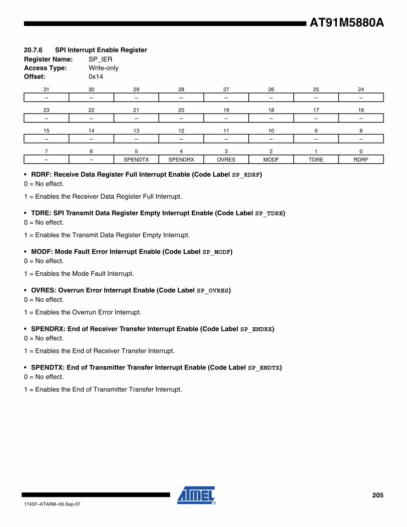
AT91M5880A
20.7.6 SPI Interrupt Enable Register Register Name: SP_IERAccess Type: Write-onlyOffset: 0x14
• RDRF: Receive Data Register Full Interrupt Enable (Code Label SP_RDRF)0 = No effect.
1 = Enables the Receiver Data Register Full Interrupt.
• TDRE: SPI Transmit Data Register Empty Interrupt Enable (Code Label SP_TDRE)0 = No effect.
1 = Enables the Transmit Data Register Empty Interrupt.
• MODF: Mode Fault Error Interrupt Enable (Code Label SP_MODF)0 = No effect.
1 = Enables the Mode Fault Interrupt.
• OVRES: Overrun Error Interrupt Enable (Code Label SP_OVRES)0 = No effect.
1 = Enables the Overrun Error Interrupt.
• SPENDRX: End of Receiver Transfer Interrupt Enable (Code Label SP_ENDRX)0 = No effect.
1 = Enables the End of Receiver Transfer Interrupt.
• SPENDTX: End of Transmitter Transfer Interrupt Enable (Code Label SP_ENDTX)0 = No effect.
1 = Enables the End of Transmitter Transfer Interrupt.
31 30 29 28 27 26 25 24
– – – – – – – –
23 22 21 20 19 18 17 16
– – – – – – – –
15 14 13 12 11 10 9 8
– – – – – – – –
7 6 5 4 3 2 1 0
– – SPENDTX SPENDRX OVRES MODF TDRE RDRF
2051745F–ATARM–06-Sep-07

20.7.7 SPI Interrupt Disable Register Register Name: SP_IDRAccess Type: Write-onlyOffset: 0x18
• RDRF: Receive Data Register Full Interrupt Disable (Code Label SP_RDRF)0 = No effect.
1 = Disables the Receiver Data Register Full Interrupt.
• TDRE: Transmit Data Register Empty Interrupt Disable (Code Label SP_TDRE)0 = No effect.
1 = Disables the Transmit Data Register Empty Interrupt.
• MODF: Mode Fault Interrupt Disable (Code Label SP_MODF)0 = No effect.
1 = Disables the Mode Fault Interrupt.
• OVRES: Overrun Error Interrupt Disable (Code Label SP_OVRES)0 = No effect.
1 = Disables the Overrun Error Interrupt.
• SPENDRX: End of Receiver Transfer Interrupt Disable (Code Label SP_ENDRX)0 = No effect.
1 = Disables the End of Receiver Transfer Interrupt.
• SPENDTX: End of Transmitter Transfer Interrupt Disable (Code Label SP_ENDTX)0 = No effect.
1 = Disables the End of Transmitter Transfer Interrupt.
31 30 29 28 27 26 25 24
– – – – – – – –
23 22 21 20 19 18 17 16
– – – – – – – –
15 14 13 12 11 10 9 8
– – – – – – – –
7 6 5 4 3 2 1 0
– – SPENDTX SPENDRX OVRES MODF TDRE RDRF
2061745F–ATARM–06-Sep-07
AT91M5880A

AT91M5880A
20.7.8 SPI Interrupt Mask Register Register Name: SP_IMRAccess Type: Read-onlyReset State: 0Offset: 0x1C
• RDRF: Receive Data Register Full Interrupt Mask (Code Label SP_RDRF)0 = Receive Data Register Full Interrupt is disabled.
1 = Receive Data Register Full Interrupt is enabled.
• TDRE: Transmit Data Register Empty Interrupt Mask (Code Label SP_TDRE)0 = Transmit Data Register Empty Interrupt is disabled.
1 = Transmit Data Register Empty Interrupt is enabled.
• MODF: Mode Fault Interrupt Mask (Code Label SP_MODF)0 = Mode Fault Interrupt is disabled.
1 = Mode Fault Interrupt is enabled.
• OVRES: Overrun Error Interrupt Mask (Code Label SP_OVRES)0 = Overrun Error Interrupt is disabled.
1 = Overrun Error Interrupt is enabled.
• SPENDRX: End of Receiver Transfer Interrupt Mask (Code Label SP_ENDRX)0 = End of Receiver Transfer Interrupt is disabled.
1 = End of Receiver Transfer Interrupt is enabled.
• SPENDTX: End of Transmitter Transfer Interrupt Mask (Code Label SP_ENDTX)0 = End of Transmitter Transfer Interrupt is disabled.
1 = End of Transmitter Transfer Interrupt is enabled.
31 30 29 28 27 26 25 24
– – – – – – – –
23 22 21 20 19 18 17 16
– – – – – – – –
15 14 13 12 11 10 9 8
– – – – – – – –
7 6 5 4 3 2 1 0
– – SPENDTX SPENDRX OVRES MODF TDRE RDRF
2071745F–ATARM–06-Sep-07

20.7.9 SPI Receive Pointer RegisterName: SP_RPRAccess Type: Read/WriteReset State: 0Offset: 0x20
• RXPTR: Receive PointerRXPTR must be loaded with the address of the receive buffer.
20.7.10 SPI Receive Counter RegisterName: SP_RCRAccess Type: Read/WriteReset State: 0Offset: 0x24
• RXCTR: Receive CounterRXCTR must be loaded with the size of the receive buffer.
0: Stop Peripheral Data Transfer dedicated to the receiver.
1 - 65535: Start Peripheral Data transfer if RDRF is active.
31 30 29 28 27 26 25 24
RXPTR
23 22 21 20 19 18 17 16
RXPTR
15 14 13 12 11 10 9 8
RXPTR
7 6 5 4 3 2 1 0
RXPTR
31 30 29 28 27 26 25 24
– – – – – – – –
23 22 21 20 19 18 17 16
– – – – – – – –
15 14 13 12 11 10 9 8
RXCTR
7 6 5 4 3 2 1 0
RXCTR
2081745F–ATARM–06-Sep-07
AT91M5880A

AT91M5880A
20.7.11 SPI Transmit Pointer RegisterName: SP_TPRAccess Type: Read/WriteReset State: 0Offset: 0x28
• TXPTR: Transmit PointerTXPTR must be loaded with the address of the transmit buffer.
20.7.12 SPI Transmit Counter RegisterName: SP_TCRAccess Type: Read/WriteReset State: 0Offset: 0x2C
• TXCTR: Transmit CounterTXCTR must be loaded with the size of the transmit buffer.
0: Stop Peripheral Data Transfer dedicated to the transmitter.
1 - 65535: Start Peripheral Data transfer if TDRE is active.
31 30 29 28 27 26 25 24
TXPTR
23 22 21 20 19 18 17 16
TXPTR
15 14 13 12 11 10 9 8
TXPTR
7 6 5 4 3 2 1 0
TXPTR
31 30 29 28 27 26 25 24
– – – – – – – –
23 22 21 20 19 18 17 16
– – – – – – – –
15 14 13 12 11 10 9 8
TXCTR
7 6 5 4 3 2 1 0
TXCTR
2091745F–ATARM–06-Sep-07

20.7.13 SPI Chip Select RegisterRegister Name: SP_CSR0.. SP_CSR3Access Type: Read/WriteReset State: 0Offset: 0x30......0x3C
• CPOL: Clock Polarity (Code Label SP_CPOL)0 = The inactive state value of SPCK is logic level zero.
1 = The inactive state value of SPCK is logic level one.
CPOL is used to determine the inactive state value of the serial clock (SPCK). It is used with NCPHA to produce a desiredclock/data relationship between master and slave devices.
• NCPHA: Clock Phase (Code Label SP_NCPHA)0 = Data is changed on the leading edge of SPCK and captured on the following edge of SPCK.
1 = Data is captured on the leading edge of SPCK and changed on the following edge of SPCK.
NCPHA determines which edge of SPCK causes data to change and which edge causes data to be captured. NCPHA isused with CPOL to produce a desired clock/data relationship between master and slave devices.
• BITS: Bits Per Transfer The BITS field determines the number of data bits transferred. Reserved values should not be used.
31 30 29 28 27 26 25 24
DLYBCT
23 22 21 20 19 18 17 16
DLYBS
15 14 13 12 11 10 9 8
SCBR
7 6 5 4 3 2 1 0
BITS – – NCPHA CPOL
BITS[3:0] Bits Per Transfer Code Label: SP_BITS0000 8 SP_BITS_8
0001 9 SP_BITS_9
0010 10 SP_BITS_10
0011 11 SP_BITS_11
0100 12 SP_BITS_12
0101 13 SP_BITS_13
0110 14 SP_BITS_14
0111 15 SP_BITS_15
1000 16 SP_BITS_16
1001 Reserved –
1010 Reserved –
1011 Reserved –
1100 Reserved –
1101 Reserved –
1110 Reserved –
1111 Reserved –
2101745F–ATARM–06-Sep-07
AT91M5880A

AT91M5880A
• SCBR: Serial Clock Baud Rate (Code Label SP_SCBR)In Master Mode, the SPI Interface uses a modulus counter to derive the SPCK baud rate from the SPI Master Clock(selected between MCK and MCK/32). The Baud rate is selected by writing a value from 2 to 255 in the field SCBR. Thefollowing equation determines the SPCK baud rate:
Giving SCBR a value of zero or one disables the baud rate generator. SPCK is disabled and assumes its inactive statevalue. No serial transfers may occur. At reset, baud rate is disabled.
• DLYBS: Delay Before SPCK (Code Label SP_DLYBS)This field defines the delay from NPCS valid to the first valid SPCK transition.
When DLYBS equals zero, the NPCS valid to SPCK transition is 1/2 the SPCK clock period.
Otherwise, the following equation determines the delay:
NPCS_to_SPCK_Delay = DLYBS * SPI_Master_Clock_period
• DLYBCT: Delay Between Consecutive Transfers (Code Label SP_DLYBCT)This field defines the delay between two consecutive transfers with the same peripheral without removing the chip select.The delay is always inserted after each transfer and before removing the chip select if needed.
When DLYBCT equals zero, a delay of four SPI Master Clock periods are inserted.
Otherwise, the following equation determines the delay:
Delay_After_Transfer = 32 * DLYBCT * SPI_Master_Clock_period
SPCK_Baud_Rate = SPI_Master_Clock_frequency
2 x SCBR
2111745F–ATARM–06-Sep-07

21. ADC: Analog-to-digital ConverterThe AT91M55800A features two identical 4-channel 10-bit Analog-to-digital converters (ADC)based on a Successive Approximation Register (SAR) approach.
Each ADC has 4 analog input pins (AD0 to AD3 and AD4 to AD7), digital trigger input pins(AD0TRIG and AD1TRIG), and provides an interrupt signal to the AIC. Both ADCs share theanalog power supply pins (VDDA and GNDA) and the input reference voltage pin (ADVREF).
Figure 21-1. Block Diagram
ADIRQ0
ADIRQ1
ADC 1Analog-to-digital Converter
ADC 0Analog-to-digital Converter
APBAdvancedPeripheral
Bus
AD0TRIG
AD0
AD1
AD2
AD3
VDDA
ADVREF
GNDA
AD4
AD5
AD6
AD7
AD1TRIG
Table 21-1. ADC Pin Description
Pin Name Description
VDDA Analog power supply
GNDA Analog ground
ADVREF Reference voltage
AD0 - AD7 Analog input channels
AD0TRIG, AD1TRIG External triggers
2121745F–ATARM–06-Sep-07
AT91M5880A

AT91M5880A
21.0.1 Analog-to-digital ConversionThe ADC has an internal sample-and-hold circuit that holds the sampled analog value during acomplete conversion.
The reference voltage pin ADVREF allows the analog input conversion range to be set between0 and ADVREF. Analog inputs between these voltages convert to values based on a linearconversion.
The ADC uses the ADC Clock to perform the conversion. To convert a single analog value to a10-bit digital data requires 11 ADC clock cycles. The ADC Clock frequency is selected in thePRESCAL field of the Mode Register (ADC_MR).
21.0.2 Conversion ResultsWhen a conversion is complete, the resulting 10-bit digital value is stored in the Convert DataRegister (ADC_CDR) of the selected channel, and the corresponding EOC flag in the StatusRegister (ADC_SR) is set. This bit can provide an interrupt signal and is automatically clearedwhen the corresponding Convert Data Register (ADC_CDR) is read.
If the ADC_CDR is not read before further incoming data is converted, the corresponding Over-run Error (OVRE) flag is set in the Status Register (ADC_SR).
The ADC offers an 8-bit or 10-bit operating mode. By default after a reset, the ADC operates in10-bit mode. If the bit RES in ADC_MR is set, the 8-bit mode is selected.
When operating in 10-bit mode, the field DATA in ADC_CDR is fully significant.
When operating in 8-bit mode, only the 8 lowest bits of DATA are significant and the 2 highestbits read 0.
21.0.3 Conversion TriggersConversions of the active analog channels are started with a software or a hardware trigger. Thesoftware trigger is provided by writing the bit START in the Control Register (ADC_CR).
The hardware trigger can be one of the TIOA outputs of the Timer Counter channels, or theexternal trigger input of the ADC (AD0TRIG for the ADC0 or AD1TRIG for ADC1). The hardwaretrigger is selected with the field TRGSEL in the Mode Register (ADC_MR). The selected hard-ware trigger is enabled with the bit TRGEN in the Mode Register (ADC_MR).
If a hardware trigger is selected, the start of a conversion is detected at each rising edge of theselected signal. If one of the TIOA outputs is selected, the corresponding Timer Counter channelmust be programmed in Waveform Mode.
Only one start command is necessary to initiate a conversion sequence on all the channels. TheADC hardware logic automatically performs the conversions on the active channels, then waitsfor a new request. The Channel Enable (ADC_CHER) and Channel Disable (ADC_CHDR) Reg-isters enable the analog channels to be enabled or disabled independently.
21.0.4 Sleep ModeThe AT91 ADC Sleep Mode maximizes power saving by deactivating the ADC when it is notbeing used for conversions. Sleep Mode is selected by setting the bit SLEEP in the Mode Regis-ter ADC_MR.
When a start conversion request occurs, the ADC is automatically activated. As the analog cellrequires a start-up time, the logic waits during this time and starts the conversion sequence on
2131745F–ATARM–06-Sep-07

the enabled channel. When all conversions are complete, the ADC is deactivated until the nexttrigger.
This permits an automatic conversion sequence with minimum CPU intervention and optimizedpower consumption.
2141745F–ATARM–06-Sep-07
AT91M5880A

AT91M5880A
21.0.5 ADC User InterfaceBase Address ADC 0:0xFFFB0000 (Code Label ADC0_BASE)Base Address ADC 1:0xFFFB4000 (Code Label ADC1_BASE)
Table 21-2. Register Mapping
Offset Register Name Access Reset
0x00 Control Register ADC_CR Write-only –
0x04 Mode Register ADC_MR Read/Write 0
0x08 Reserved – – –
0x0C Reserved – – –
0x10 Channel Enable Register ADC_CHER Write-only –
0x14 Channel Disable Register ADC_CHDR Write-only –
0x18 Channel Status Register ADC_CHSR Read-only 0
0x1C Reserved – – –
0x20 Status Register ADC_SR Read-only 0
0x24 Interrupt Enable Register ADC_IER Write-only –
0x28 Interrupt Disable Register ADC_IDR Write-only –
0x2C Interrupt Mask Register ADC_IMR Read-only 0
0x30 Convert Data Register 0 ADC_CDR0 Read-only 0
0x34 Convert Data Register 1 ADC_CDR1 Read-only 0
0x38 Convert Data Register 2 ADC_CDR2 Read-only 0
0x3C Convert Data Register 3 ADC_CDR3 Read-only 0
2151745F–ATARM–06-Sep-07

21.0.6 ADC Control Register Register Name: ADC_CRAccess Type: Write-onlyOffset: 0x00
• SWRST: Software Reset (Code Label ADC_SWRST)0 = No effect.
1 = Resets the ADC simulating a hardware reset.
• START: Start Conversion (Code Label ADC_START)0 = No effect.
1 = Begins analog-to-digital conversion and clears all EOC bits.
31 30 29 28 27 26 25 24
– – – – – – – –
23 22 21 20 19 18 17 16
– – – – – – – –
15 14 13 12 11 10 9 8
– – – – – – – –
7 6 5 4 3 2 1 0
– – – – – – START SWRST
2161745F–ATARM–06-Sep-07
AT91M5880A

AT91M5880A
21.0.7 ADC Mode RegisterRegister Name: ADC_MRAccess Type: Read/WriteReset State: 0Offset: 0x04
• TRGEN: Trigger Enable
• TRGSEL: Trigger SelectionThis field selects the hardware trigger.
• RES: Resolution.
31 30 29 28 27 26 25 24
– – – – – – – –
23 22 21 20 19 18 17 16
– – – – – – – –
15 14 13 12 11 10 9 8
– – PRESCAL
7 6 5 4 3 2 1 0
– – SLEEP RES TRGSEL TRGEN
TRGEN Selected TRGEN Code Label
0Hardware triggers are disabled. Starting a conversion is only possible by software.
ADC_TRGEN_DIS
1 Hardware trigger selected by TRGSEL field is enabled. ADC_TRGEN_EN
TTRGSEL Selected TRGSEL Code Label: ADC_B_TTRGSEL
0 0 0 TIOA0 ADC_TRG_TIOA0
0 0 1 TIOA1 ADC_TRG_TIOA1
0 1 0 TIOA2 ADC_TRG_TIOA2
0 1 1 TIOA3 ADC_TRG_TIOA3
1 0 0 TIOA4 ADC_TRG_TIOA4
1 0 1 TIOA5 ADC_TRG_TIOA5
1 1 0 External trigger ADC_TRG_EXT
1 1 1 Reserved –
RES Selected RES Code Label
0 10-bit resolution ADC_10_BIT_RES
1 8-bit resolution ADC_8_BIT_RES
2171745F–ATARM–06-Sep-07

• SLEEP: Sleep Mode
• PRESCAL: Prescaler Rate Selection (ADC_PRESCAL)This field defines the conversion clock in function of the Master Clock (MCK):
The ADC clock range is between MCK/2 (PRESCAL = 0) and MCK /128 (PRESCAL = 63). PRESCAL must be pro-grammed in order to provide an ADC clock frequency according to the parameters given in the AT91M55800A ElectricalDatasheet, literature number 1727.
SLEEP Selected SLEEP Code Label
0 Normal Mode ADC_NORMAL_MODE
1 Sleep Mode ADC_SLEEP_MODE
ADCClock MCK ((PRESCAL +1)⁄ 2× )=
2181745F–ATARM–06-Sep-07
AT91M5880A

AT91M5880A
21.0.8 ADC Channel Enable Register Register Name: ADC_CHERAccess Type: Write-onlyOffset: 0x10
• CH: Channel Enable (Code Label ADC_CHx)0 = No effect.
1 = Enables the corresponding channel.
21.0.9 ADC Channel Disable Register Register Name: ADC_CHDRAccess Type: Write-onlyOffset: 0x14
• CH: Channel Disable (Code Label ADC_CHx)0 = No effect.
1 = Disables the corresponding channel.
31 30 29 28 27 26 25 24
– – – – – – – –
23 22 21 20 19 18 17 16
– – – – – – – –
15 14 13 12 11 10 9 8
– – – – – – – –
7 6 5 4 3 2 1 0
– – – – CH3 CH2 CH1 CH0
31 30 29 28 27 26 25 24
– – – – – – – –
23 22 21 20 19 18 17 16
– – – – – – – –
15 14 13 12 11 10 9 8
– – – – – – – –
7 6 5 4 3 2 1 0
– – – – CH3 CH2 CH1 CH0
2191745F–ATARM–06-Sep-07

21.0.10 ADC Channel Status Register Register Name: ADC_CHSRAccess Type: Read-onlyReset State: 0Offset: 0x18
• CH: Channel Status (Code Label ADC_CHx)0 = Corresponding channel is disabled.
1 = Corresponding channel is enabled.
21.0.11 ADC Status Register Register Name: ADC_SRAccess Type: Read-onlyReset State: 0Offset: 0x20
• EOC: End of Conversion (Code Label ADC_EOCx)0 = Corresponding analog channel is disabled, or the conversion is not finished.
1 = Corresponding analog channel is enabled and conversion is complete.
• OVRE: Enable Overrun Error Interrupt (Code Label ADC_OVREx)0 = No overrun on the corresponding channel since the last read of ADC_SR.
1 = There has been an overrun on the corresponding channel since the last read of ADC_SR.
31 30 29 28 27 26 25 24
– – – – – – – –
23 22 21 20 19 18 17 16
– – – – – – – –
15 14 13 12 11 10 9 8
– – – – – – – –
7 6 5 4 3 2 1 0
– – – – CH3 CH2 CH1 CH0
31 30 29 28 27 26 25 24
– – – – – – – –
23 22 21 20 19 18 17 16
– – – – – – – –
15 14 13 12 11 10 9 8
– – – – OVRE3 OVRE2 OVRE1 OVRE0
7 6 5 4 3 2 1 0
– – – – EOC3 EOC2 EOC1 EOC0
2201745F–ATARM–06-Sep-07
AT91M5880A

AT91M5880A
21.0.12 ADC Interrupt Enable Register Register Name: ADC_IERAccess Type: Write-onlyOffset: 0x24
• EOC: End of Conversion Interrupt Enable (Code Label ADC_EOCx)0 = No effect.
1 = Enables the End of Conversion Interrupt.
• OVRE: Overrun Error Interrupt Enable (Code Label ADC_OVREx)0 = No effect.
1 = Enables the Overrun Error Interrupt.
21.0.13 ADC Interrupt Disable Register Register Name: ADC_IDRAccess Type: Write-onlyOffset: 0x28
• EOC: End of Conversion Interrupt Disable (Code Label ADC_EOCx)0 = No effect.
1 = Disables the End of Conversion Interrupt.
• OVRE: Overrun Error Interrupt Disable (Code Label ADC_OVREx)0 = No effect.
1 = Disables the Overrun Error Interrupt.
31 30 29 28 27 26 25 24
– – – – – – – –
23 22 21 20 19 18 17 16
– – – – – – – –
15 14 13 12 11 10 9 8
– – – – OVRE3 OVRE2 OVRE1 OVRE0
7 6 5 4 3 2 1 0
– – – – EOC3 EOC2 EOC1 EOC0
31 30 29 28 27 26 25 24
– – – – – – – –
23 22 21 20 19 18 17 16
– – – – – – – –
15 14 13 12 11 10 9 8
– – – – OVRE3 OVRE2 OVRE1 OVRE0
7 6 5 4 3 2 1 0
– – – – EOC3 EOC2 EOC1 EOC0
2211745F–ATARM–06-Sep-07

21.0.14 ADC Interrupt Mask Register Register Name: ADC_IMRAccess Type: Read-onlyReset State: 0Offset: 0x2C
• EOC: End of Conversion Interrupt Mask (Code Label ADC_EOCx)0 = End of Conversion Interrupt is disabled.
1 = End of Conversion Interrupt is enabled.
• OVRE: Overrun Error Interrupt Mask (Code Label ADC_OVREx)0 = Overrun Error Interrupt is disabled.
1 = Overrun Error Interrupt is enabled.
31 30 29 28 27 26 25 24
– – – – – – – –
23 22 21 20 19 18 17 16
– – – – – – – –
15 14 13 12 11 10 9 8
– – – – OVRE3 OVRE2 OVRE1 OVRE0
7 6 5 4 3 2 1 0
– – – – EOC3 EOC2 EOC1 EOC0
2221745F–ATARM–06-Sep-07
AT91M5880A

AT91M5880A
21.0.15 ADC Convert Data RegisterRegister Name: ADC_CDR0 to ADC_CDR3Access Type: Read-onlyReset State: 0Offset: 0x30 to 0x3C
• DATA: Converted DataThe analog-to-digital conversion data is placed into this register at the end of a conversion and remains until a new conver-sion is completed. The Convert Data Register (CDR) is only loaded if the corresponding analog channel is enabled.
31 30 29 28 27 26 25 24
– – – – – – – –
23 22 21 20 19 18 17 16
– – – – – – – –
15 14 13 12 11 10 9 8
– – – – – – DATA
7 6 5 4 3 2 1 0
DATA
DATA Selected DATA Code Label: ADC_CDRx
0 or 1 10-bits Data ADC_DATA_10BITS
0 or 1 8-bits Data ADC_DATA_8BITS
2231745F–ATARM–06-Sep-07

22. DAC: Digital-to-Analog ConverterThe AT91M55800A features two identical 1-channel 10-bit Digital-to-analog converters (DAC).
Each DAC has an analog output pin (DA0 and DA1) and provides an interrupt signal to the AIC(DA0IRQ and DA1IRQ). Both DACs share the analog power supply pins VDDA and GNDA, andthe input reference pin DAVREF.
Figure 22-1. DAC Block Diagram
22.1 Conversion DetailsDigital-to-analog conversions are possible only if the DAC has been enabled in the APMC andthe startup time has elapsed. This startup time is a maximum of 5 µsec, and is indicated moreprecisely in the Electrical Characteristics datasheet of the device as parameter tDASU.
Digital inputs are converted to output voltages on a linear conversion between 0 and DAVREF.The analog output voltages on DA0 and DA1 pins are determined by the following equation:
Table 22-1.
Pin Name Meaning
VDDA Analog power supply
GNDA Analog ground
DAVREF Reference voltage
DA0 Analog output, channel 0
DA1 Analog output, channel 1
+
-
Data Holding Register
Data OutputRegister
Control Logic
Trigger Selection
10-bit DAC
VDDA
GNDA
DAn
DAVREF
DAnIRQ
AdvancedPeripheral Bus
TIOA0....TIOA5
2241745F–ATARM–06-Sep-07
AT91M5880A

AT91M5880A
DA = DAVREF x (DAC_DOR / 1024)
When DAC_DOR (Data Output Register) is loaded, the analog output voltage is available after asettling time of approximately 5 µsec. The exact value depends on the power supply voltage andthe analog output load, and is indicated in the Electrical Characteristics Sheet of the device asparameter tDAST.
The output register cannot be written directly and any data transfer to the DAC must be per-formed by writing in DAC_DHR (Data Holding Register). The transfer from DAC_DHR toDAC_DOR is performed automatically or when an hardware trigger occurs, depending on the bitTRGEN in DAC_MR (Mode Register).
The DAC integrates an output buffer enabling the reduction of the output impedance, and thepossibility of driving external loads directly, without having to add an external operational ampli-fier. The maximum load supported by the output buffer is indicated in the ElectricalCharacteristics of the device.
22.1.1 8- or 10-bit Conversion ModeBit RES in the Mode Register (DAC_MR) selects between 8-bit or 10-bit modes of operation. In8-bit mode, the data written in DAC_DHR is automatically shifted left two bits and the two lowestbits are written 0. The bit RES also affects the type of transfers performed by the PDC channel:
• in 8-bit mode, only a byte transfer is performed.
• in 10-bit mode, a half-word transfer (16 bits) is performed.
22.1.2 Trigger SelectionA conversion is triggered when data is written in DAC_DHR and TRGEN in DAC_MR is 0.
If TRGEN is 1, a hardware trigger is selected by the field TTRGSEL between the Timer CounterChannel outputs TIOA. In this case, the corresponding Timer Counter channel must be pro-grammed in Waveform Mode, and each time the DAC detects a rising edge on the TC output, ittransfers the last data written in DAC_DHR into DAC_DOR.
The bit DATRDY traces the fact that a valid data has been written in DAC_DHR and not yetbeen transferred in DAC_DOR. An interrupt can be generated from this status bit to tell the soft-ware to load the following value.
2251745F–ATARM–06-Sep-07

22.2 DAC User InterfaceBase Address DAC 0:0xFFFA8000 (Code Label DAC0_BASE)Base Address DAC 1:0xFFFAC000 (Code Label DAC1_BASE)
Table 22-2. Register Mapping
Offset Register Name Access Reset
0x00 Control Register DAC_CR Write-only –
0x04 Mode Register DAC_MR Read/Write 0
0x08 Data Holding Register DAC_DHR Read/Write 0
0x0C Data Output Register DAC_DOR Read-only 0
0x10 Status Register DAC_SR Read-only 0
0x14 Interrupt Enable Register DAC_IER Write-only –
0x18 Interrupt Disable Register DAC_IDR Write-only –
0x1C Interrupt Mask Register DAC_IMR Read-only 0
2261745F–ATARM–06-Sep-07
AT91M5880A

AT91M5880A
22.2.1 DAC Control RegisterRegister Name: DAC_CRAccess Type: Write-onlyOffset: 0x00
• SWRST: Software Reset (Code Label DAC_SWRST)0 = No effect.
1 = Resets the DAC. A software-triggered reset of the DAC interface is performed.
31 30 29 28 27 26 25 24– – – – – – – –
23 22 21 20 19 18 17 16
– – – – – – – –
15 14 13 12 11 10 9 8
– – – – – – – –
7 6 5 4 3 2 1 0
– – – – – – – SWRST
2271745F–ATARM–06-Sep-07

22.2.2 DAC Mode RegisterRegister Name: DAC_MRAccess Type: Read/WriteReset State: 0Offset: 0x04
• TTRGEN: Timer Trigger Enable (Code Label DAC_TTRGEN_EN)
• TTRGSEL: Timer Trigger SelectionOnly used if TTRGEN = 1
• RES: Resolution
31 30 29 28 27 26 25 24
– – – – – – – –
23 22 21 20 19 18 17 16
– – – – – – – –
15 14 13 12 11 10 9 8
– – – – – – – –
7 6 5 4 3 2 1 0
– – – RES TTRGSEL TTRGEN
TTRGEN Selected TTRGEN Code Label
0The data written into the Data Holding Register (DAC_DHR) is transferred one main clock cycle later to the data output register (DAC_DOR).
DAC_TTRGEN_DIS
1The data transfer from the DAC_DHR to the DAC_DOR is synchronized by the timer trigger.
DAC_TTRGEN_EN
TTRGSEL Selected Timer Trigger
Code Label
DAC_TTRGSEL
0 0 0 TIOA0 DAC_TRG_TIOA0
0 0 1 TIOA1 DAC_TRG_TIOA1
0 1 0 TIOA2 DAC_TRG_TIOA2
0 1 1 TIOA3 DAC_TRG_TIOA3
1 0 0 TIOA4 DAC_TRG_TIOA4
1 0 1 TIOA5 DAC_TRG_TIOA5
1 1 X Reserved –
RES Selected RES Code Label
0 10-bit resolution DAC_10_BIT_RES
1 8-bit resolution DAC_8_BIT_RES
2281745F–ATARM–06-Sep-07
AT91M5880A

AT91M5880A
22.2.3 DAC Data Holding RegisterRegister Name: DAC_DHRAccess Type: Read/WriteReset State: 0Offset: 0x08
• DATA: Data to be Converted (Code Label DAC_DATA_10BITS or DAC_DATA_8BITS depending on RES)Data that is to be converted by the DAC is stored in this register. Data to be converted must be written in a right-aligned format.
In 8-bit resolution mode (RES = 1), data written into the Data Holding Register will be shifted to the left by 2 bits and the twoLSBs will be 0.
In both 8-bit and 10-bit modes, data will be read as written after the adjustments are done. All non-significant bits read 0.
31 30 29 28 27 26 25 24
– – – – – – – –
23 22 21 20 19 18 17 16
– – – – – – – –
15 14 13 12 11 10 9 8
– – – – – – DATA
7 6 5 4 3 2 1 0
DATA
2291745F–ATARM–06-Sep-07
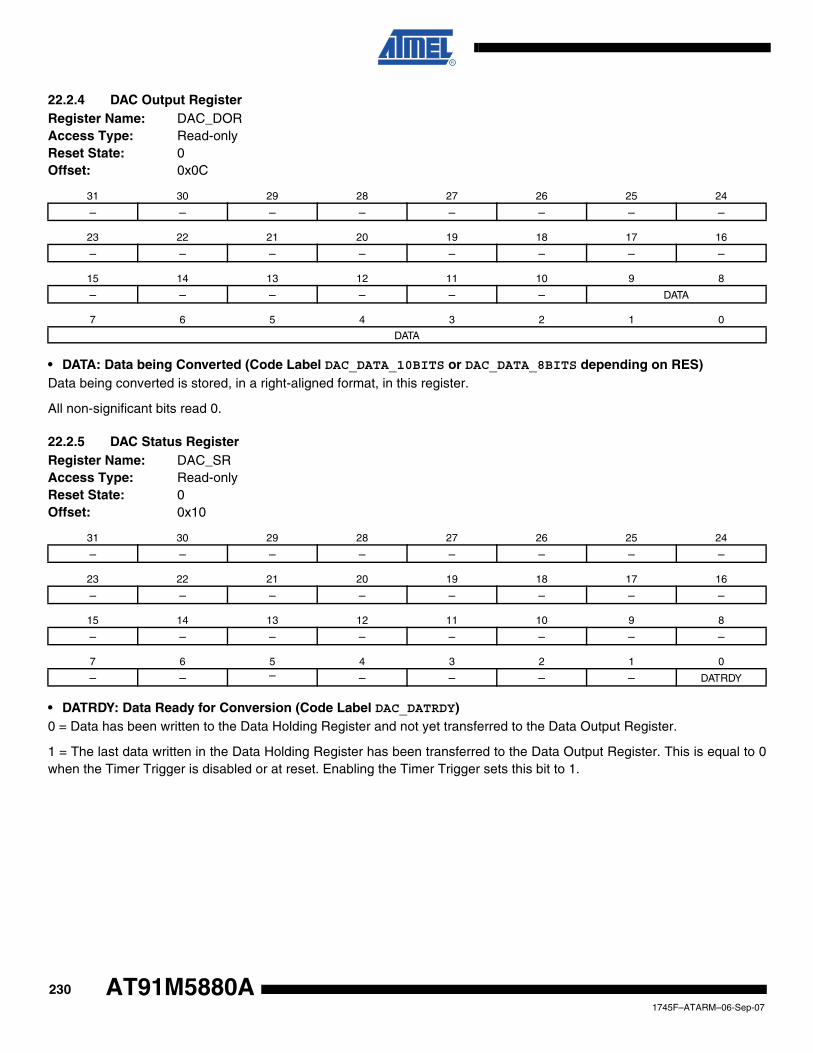
22.2.4 DAC Output RegisterRegister Name: DAC_DORAccess Type: Read-onlyReset State: 0Offset: 0x0C
• DATA: Data being Converted (Code Label DAC_DATA_10BITS or DAC_DATA_8BITS depending on RES)Data being converted is stored, in a right-aligned format, in this register.
All non-significant bits read 0.
22.2.5 DAC Status RegisterRegister Name: DAC_SRAccess Type: Read-onlyReset State: 0Offset: 0x10
• DATRDY: Data Ready for Conversion (Code Label DAC_DATRDY)0 = Data has been written to the Data Holding Register and not yet transferred to the Data Output Register.
1 = The last data written in the Data Holding Register has been transferred to the Data Output Register. This is equal to 0when the Timer Trigger is disabled or at reset. Enabling the Timer Trigger sets this bit to 1.
31 30 29 28 27 26 25 24
– – – – – – – –
23 22 21 20 19 18 17 16
– – – – – – – –
15 14 13 12 11 10 9 8
– – – – – – DATA
7 6 5 4 3 2 1 0
DATA
31 30 29 28 27 26 25 24
– – – – – – – –
23 22 21 20 19 18 17 16
– – – – – – – –
15 14 13 12 11 10 9 8
– – – – – – – –
7 6 5 4 3 2 1 0
– – – – – – – DATRDY
2301745F–ATARM–06-Sep-07
AT91M5880A

AT91M5880A
22.2.6 DAC Interrupt Enable RegisterRegister Name: DAC_IERAccess Type: Write-onlyOffset: 0x14
• DATRDY: Data Ready for Conversion Interrupt Enable (Code Label DAC_DATRDY)0 = No effect.
1 = Enables the Data Ready for Conversion Interrupt.
22.2.7 DAC Interrupt Disable RegisterRegister Name: DAC_IDRAccess Type: Write-onlyOffset: 0x18
• DATRDY: Data Ready for Conversion Interrupt Disable (Code Label DAC_DATRDY)0 = No effect.
1 = Disables the Data Ready for Conversion Interrupt.
31 30 29 28 27 26 25 24
– – – – – – – –
23 22 21 20 19 18 17 16
– – – – – – – –
15 14 13 12 11 10 9 8
– – – – – – – –
7 6 5 4 3 2 1 0
– – – – – – – DATRDY
31 30 29 28 27 26 25 24
– – – – – – – –
23 22 21 20 19 18 17 16
– – – – – – – –
15 14 13 12 11 10 9 8
– – – – – – – –
7 6 5 4 3 2 1 0
– – – – – – – DATRDY
2311745F–ATARM–06-Sep-07

22.2.8 DAC Interrupt Mask RegisterRegister Name: DAC_IMRAccess Type: Read-onlyReset State: 0Offset: 0x1C
• DATRDY: Data Ready for Conversion Interrupt Mask (Code Label DAC_DATRDY)0 = Data Ready for Conversion Interrupt is disabled.
1 = Data Ready for Conversion Interrupt is enabled.
31 30 29 28 27 26 25 24
– – – – – – – –
23 22 21 20 19 18 17 16
– – – – – – – –
15 14 13 12 11 10 9 8
– – – – – – – –
7 6 5 4 3 2 1 0
– – – – – – – DATRDY
2321745F–ATARM–06-Sep-07
AT91M5880A

AT91M5880A
23. JTAG Boundary-scan RegisterThe Boundary-scan Register (BSR) contains 256 bits which correspond to active pins and asso-ciated control signals.
Each AT91M55800A input pin has a corresponding bit in the Boundary-scan Register forobservability.
Each AT91M55800A output pin has a corresponding 2-bit register in the BSR. The OUTPUT bitcontains data which can be forced on the pad. The CTRL bit can put the pad into high imped-ance.
Each AT91M55800A in/out pin corresponds to a 3-bit register in the BSR. The OUTPUT bit con-tains data that can be forced on the pad. The INPUT bit is for the observability of data applied tothe pad. The CTRL bit selects the direction of the pad.
Table 23-1. JTAG Boundary-scan Register
Bit Number Pin Name Pin Type
Associated BSR Cells
256 NWAIT INPUT INPUT
255 NRST INPUT INPUT
254
PB18/BMS IN/OUT
OUTPUT
253 INPUT
252 CTRL
251MCKO OUTPUT
OUTPUT
250 CTRL
249NWDOVF OUTPUT
OUTPUT
248 CTRL
247
PB17 IN/OUT
OUTPUT
246 INPUT
245 CTRL
244
PB16 IN/OUT
OUTPUT
243 INPUT
242 CTRL
241
PB15 IN/OUT
OUTPUT
240 INPUT
239 CTRL
238
PB14 IN/OUT
OUTPUT
237 INPUT
236 CTRL
235PB13 IN/OUT
OUTPUT
234 INPUT
233 PB13 IN/OUT CTRL
2331745F–ATARM–06-Sep-07

232
PB12 IN/OUT
OUTPUT
231 INPUT
230 CTRL
229
PB11 IN/OUT
OUTPUT
228 INPUT
227 CTRL
226
PB10 IN/OUT
OUTPUT
225 INPUT
224 CTRL
223
PB9 IN/OUT
OUTPUT
222 INPUT
221 CTRL
220
PB8 IN/OUT
OUTPUT
219 INPUT
218 CTRL
217
PB7/AD1TRIG IN/OUT
OUTPUT
216 INPUT
215 CTRL
214
PB6/AD0TRIG IN/OUT
OUTPUT
213 INPUT
212 CTRL
211
PB5 IN/OUT
OUTPUT
210 INPUT
209 CTRL
208
PB4/IRQ5 IN/OUT
OUTPUT
207 INPUT
206 CTRL
205
PB3 IN/OUT
OUTPUT
204 INPUT
203 CTRL
202
PB2 IN/OUT
OUTPUT
201 INPUT
200 CTRL
Table 23-1. JTAG Boundary-scan Register (Continued)
Bit Number Pin Name Pin Type
Associated BSR Cells
2341745F–ATARM–06-Sep-07
AT91M5880A

AT91M5880A
199
PB1 IN/OUT
OUTPUT
198 INPUT
197 CTRL
196
PB0 IN/OUT
OUTPUT
195 INPUT
194 CTRL
193 NCS7 OUTPUT OUTPUT
192 NCS6 OUTPUT OUTPUT
191 NCS5 OUTPUT OUTPUT
190 NCS4 OUTPUT OUTPUT
189
PA29NPCS3 IN/OUT
OUTPUT
188 INPUT
187 CTRL
186
PA28NPCS2 IN/OUT
OUTPUT
185 INPUT
184 CTRL
183
PA27NPCS1 IN/OUT
OUTPUT
182 INPUT
181 CTRL
180
PA26NPCS0 IN/OUT
OUTPUT
179 INPUT
178 CTRL
177
PA25MOSI IN/OUT
OUTPUT
176 INPUT
175 CTRL
174
PA24MISO IN/OUT
OUTPUT
173 INPUT
172 CTRL
171
PA23SPCK IN/OUT
OUTPUT
170 INPUT
169 CTRL
168
PA22RXD2 IN/OUT
OUTPUT
167 INPUT
166 CTRL
165 PA21TXD2 IN/OUT OUTPUT
Table 23-1. JTAG Boundary-scan Register (Continued)
Bit Number Pin Name Pin Type
Associated BSR Cells
2351745F–ATARM–06-Sep-07

164PA21TXD2 IN/OUT
INPUT
163 CTRL
162
PA20SCK2 IN/OUT
OUTPUT
161 INPUT
160 CTRL
159
PA19RXD1 IN/OUT
OUTPUT
158 INPUT
157 CTRL
156
PA18/TXD1/NTRI IN/OUT
OUTPUT
155 INPUT
154 CTRL
153
PA17/SCK1 IN/OUT
OUTPUT
152 INPUT
151 CTRL
150
PA16/RXD0 IN/OUT
OUTPUT
149 INPUT
148 CTRL
147
PA15/TXD0 IN/OUT
OUTPUT
146 INPUT
145 CTRL
144
PA14/SCK0 IN/OUT
OUTPUT
143 INPUT
142 CTRL
141
PA13/FIQ IN/OUT
OUTPUT
140 INPUT
139 CTRL
138
PA12/IRQ3 IN/OUT
OUTPUT
137 INPUT
136 CTRL
135
PA11/IRQ2 IN/OUT
OUTPUT
134 INPUT
133 CTRL
132
PA10/IRQ1 IN/OUT
OUTPUT
131 INPUT
130 CTRL
Table 23-1. JTAG Boundary-scan Register (Continued)
Bit Number Pin Name Pin Type
Associated BSR Cells
2361745F–ATARM–06-Sep-07
AT91M5880A
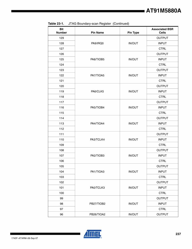
AT91M5880A
129
PA9/IRQ0 IN/OUT
OUTPUT
128 INPUT
127 CTRL
126
PA8/TIOB5 IN/OUT
OUTPUT
125 INPUT
124 CTRL
123
PA7/TIOA5 IN/OUT
OUTPUT
122 INPUT
121 CTRL
120
PA6/CLK5 IN/OUT
OUTPUT
119 INPUT
118 CTRL
117
PA5/TIOB4 IN/OUT
OUTPUT
116 INPUT
115 CTRL
114
PA4/TIOA4 IN/OUT
OUTPUT
113 INPUT
112 CTRL
111
PA3/TCLK4 IN/OUT
OUTPUT
110 INPUT
109 CTRL
108
PA2/TIOB3 IN/OUT
OUTPUT
107 INPUT
106 CTRL
105
PA1/TIOA3 IN/OUT
OUTPUT
104 INPUT
103 CTRL
102
PA0/TCLK3 IN/OUT
OUTPUT
101 INPUT
100 CTRL
99
PB27/TIOB2 IN/OUT
OUTPUT
98 INPUT
97 CTRL
96 PB26/TIOA2 IN/OUT OUTPUT
Table 23-1. JTAG Boundary-scan Register (Continued)
Bit Number Pin Name Pin Type
Associated BSR Cells
2371745F–ATARM–06-Sep-07

95 INPUT
94 CTRL
93
PB25/TCLK2 IN/OUT
OUTPUT
92 INPUT
91 CTRL
90
PB24/TIOB1 IN/OUT
OUTPUT
89 INPUT
88 CTRL
87
PB23/TIOA1 IN/OUT
OUTPUT
86 INPUT
85 CTRL
84
PB22/TCLK1 IN/OUT
OUTPUT
83 INPUT
82 CTRL
81
PB21TIOB0 IN/OUT
OUTPUT
80 INPUT
79 CTRL
78
PB20/TIOA0 IN/OUT
OUTPUT
77 INPUT
76 CTRL
75
PB19/TCLK0 IN/OUT
OUTPUT
74 INPUT
73 CTRL
72D15 IN/OUT
INPUT
71 OUTPUT
70D14 IN/OUT
INPUT
69 OUTPUT
68D13 IN/OUT
INPUT
67 OUTPUT
66D12 IN/OUT
INPUT
65 OUTPUT
64D11 IN/OUT
INPUT
63 OUTPUT
62D10 IN/OUT
INPUT
61 OUTPUT
Table 23-1. JTAG Boundary-scan Register (Continued)
Bit Number Pin Name Pin Type
Associated BSR Cells
2381745F–ATARM–06-Sep-07
AT91M5880A

AT91M5880A
60D9 IN/OUT
INPUT
59 OUTPUT
58D8 IN/OUT
INPUT
57 OUTPUT
56 D[15:8] IN/OUT CTRL
55D7 IN/OUT
INPUT
54 OUTPUT
53D6 IN/OUT
INPUT
52 OUTPUT
51D5 IN/OUT
INPUT
50 OUTPUT
49D4 IN/OUT
INPUT
48 OUTPUT
47D3 IN/OUT
INPUT
46 OUTPUT
45D2 IN/OUT
INPUT
44 OUTPUT
43D1 IN/OUT
INPUT
42 OUTPUT
41D0
IN/OUT INPUT
40 OUTPUT
39 D[7:0] IN/OUT CTRL
38 A23 OUTPUT OUTPUT
37 A22 OUTPUT OUTPUT
36 A21 OUTPUT OUTPUT
35 A20 OUTPUT OUTPUT
34 A19 OUTPUT OUTPUT
33 A18 OUTPUT OUTPUT
32 A17 OUTPUT OUTPUT
31 A16 OUTPUT OUTPUT
30 A[23:16] OUTPUT CTRL
29 A15 OUTPUT OUTPUT
28 A14 OUTPUT OUTPUT
27 A13 OUTPUT OUTPUT
26 A12 OUTPUT OUTPUT
Table 23-1. JTAG Boundary-scan Register (Continued)
Bit Number Pin Name Pin Type
Associated BSR Cells
2391745F–ATARM–06-Sep-07

25 A11 OUTPUT OUTPUT
24 A10 OUTPUT OUTPUT
23 A9 OUTPUT OUTPUT
22 A8 OUTPUT OUTPUT
21 A[15:8] OUTPUT CTRL
20 A7 OUTPUT OUTPUT
19 A6 OUTPUT OUTPUT
18 A5 OUTPUT OUTPUT
17 A4 OUTPUT OUTPUT
16 A3 OUTPUT OUTPUT
15 A2 OUTPUT OUTPUT
14 A1 OUTPUT OUTPUT
13 NLB/A0 OUTPUT OUTPUT
12 A[7:0] OUTPUT CTRL
11 NCS3 OUTPUT OUTPUT
10 NCS2 OUTPUT OUTPUT
9 NCS1 OUTPUT OUTPUT
8 NCS0 OUTPUT OUTPUT
7NUB/NWR1 IN/OUT
OUTPUT
6 INPUT
5NUB/NWR0 IN/OUT
OUTPUT
4 INPUT
3NOE/NRD IN/OUT
OUTPUT
2 INPUT
1
NCS[7:0]NUB/NWR1
NWE/NWR0
NOE/NRD
IN/OUT CTRL
Table 23-1. JTAG Boundary-scan Register (Continued)
Bit Number Pin Name Pin Type
Associated BSR Cells
AT91M55800A-33AIAT91M55800A-33AUAT91M55800A-33CIAT91M55800A-33CJ
Internal ProductReference 56515B
2401745F–ATARM–06-Sep-07
AT91M5880A

AT91M5880A
24. Packaging Information
Figure 24-1. 176-lead Thin Quad Flat Pack Package Drawing
PIN 1
aaa
bbb
c c1
ddd
θ2
θ3
S
L1
R1 R20.25
θ
ccc
θ1
2411745F–ATARM–06-Sep-07

Table 24-1. Common Dimensions (mm)
Symbol Min Nom Max
c 0.09 0.20
c1 0.09 0.16
L 0.45 0.6 0.75
L1 1.00 REF
R2 0.08 0.2
R1 0.08
S 0.2
q 0° 3.5° 7°
θ1 0°
θ2 11° 12° 13°
θ3 11° 12° 13°
A 1.6
A1 0.05 0.15
A2 1.35 1.4 1.45
Tolerances of form and position
aaa 0.2
bbb 0.2
Table 24-2. Lead Count Dimensions (mm)
Pin Count
D/E BSC
D1/E1 BSC
b b1e
BSC ccc dddMin Nom Max Min Nom Max
176 26.0 24.0 0.17 0.20 0.27 0.17 0.20 0.23 0.50 0.10 0.08
Table 24-3. Device and 176-lead LQFP Package Maximum Weight
2023 mg
2421745F–ATARM–06-Sep-07
AT91M5880A

AT91M5880A
Figure 24-2. 176-ball Ball Grid Array Package Drawing
Table 24-4. Device and 176-ball BGA Package Maximum Weight
606 mg
Notes: 1. Package dimensions conform to JEDEC MO-205
2. Dimensioning and tolerancing per ASME Y14.5M-1994
3. All dimensions in mm
4. Solder Ball position designation per JESD 95-1, SPP-010
5. Primary datum Z and seating plane are defined by the spherical crowns of the solder balls
Symbol Maximum
aaa 0.1
bbb 0.1
ddd 0.1
eee 0.03
fff 0.04
ggg 0.03
hhh 0.1
kkk 0.1
Top View
Bottom View
2431745F–ATARM–06-Sep-07

25. Soldering Profile
25.1 LQFP Soldering Profile (Green)Table 25-1 gives the recommended soldering profile from J-STD-020C.
Note: The package is certified to be backward compatible with Pb/Sn soldering profile.
A maximum of three reflow passes is allowed per component.
25.2 BGA Soldering Profile (RoHS-compliant)Table 25-2 gives the recommended soldering profile from J-STD-20C.
Note: It is recommended to apply a soldering temperature higher than 250°C.
A maximum of three reflow passes is allowed per component.
Table 25-1. Soldering Profile Green Compliant Package
Profile Feature Green Package
Average Ramp-up Rate (217°C to Peak) 3°C/sec. max.
Preheat Temperature 175°C ±25°C 180 sec. max.
Temperature Maintained Above 217°C 60 sec. to 150 sec.
Time within 5°C of Actual Peak Temperature 20 sec. to 40 sec.
Peak Temperature Range 260 +0 °C
Ramp-down Rate 6°C/sec. max.
Time 25°C to Peak Temperature 8 min. max.
Table 25-2. Soldering Profile RoHS Compliant Package
Profile Feature Convection or IR/Convection
Average Ramp-up Rate (183°C to Peak) 3°C/sec. max.
Preheat Temperature 125°C ±25°C 180 sec. max
Temperature Maintained Above 183°C 60 sec. to 150 sec.
Time within 5°C of Actual Peak Temperature 20 sec. to 40 sec.
Peak Temperature Range 260 + 0°C
Ramp-down Rate 6°C/sec.
Time 25°C to Peak Temperature 8 min. max
2441745F–ATARM–06-Sep-07
AT91M5880A

AT91M5880A
26. Ordering Information
Table 26-1. Ordering Information
Ordering Code Package Package TypeTemperature
Operating Range
AT91M55800A-33AU LQFP 176 GreenIndustrial
(-40°C to 85°C)
AT91M55800A-33CJ BGA 176 RoHS-compliant
2451745F–ATARM–06-Sep-07

27. Errata The following known errata are applicable to:
• The following datasheets:
AT91M55800A Summary, 1745S
AT91M55800A, (This document)
AT91M55800A, Electrical Characteristics Rev.1727
• 176-lead LQFP and 176-ball BGA devices with the following markings:
27.1 ADC: ADC Characteristics and BehaviorThe tracking time has a theoretical minimum duration. It equals one ADC Clock period and isnormally ensured by the ADC Controller.
It might randomly happen that this minimum duration cannot be guaranteed on the first enabledchannel. When this happens, the sampling and hold process is too short and the conversionresult is wrong.
Problem Fix/Work AroundTo use only one channel, the user has to enable two channels and then must use the secondchannel only.
In the event that all of the ADC channels need to be used, only three channels will be available.
A software work around allows all the channels to be used. It consists of performing several con-versions and averaging the samples on the first enabled channel. This method does not supportfast conversion. However, signals from temperature sensors, which are slow signals, can behandled by averaging a number of samples.
27.2 Warning: Additional NWAIT ConstraintsWhen the NWAIT signal is asserted during an external memory access, the following EBIbehavior is correct:
– NWAIT is asserted before the first rising edge of the master clock and respects the NWAIT to MCKI rising setup timing as defined in the Electrical Characteristics datasheet.
– NWAIT is sampled inactive and at least one standard wait state remains to be executed, even if NWAIT does not meet the NWAIT to first MCKI rising setup timing (i.e., NWAIT is asserted only on the second rising edge of MCKI).
In these cases, the access is delayed as required by NWAIT and the access operations arecorrectly performed.
2461745F–ATARM–06-Sep-07
AT91M5880A
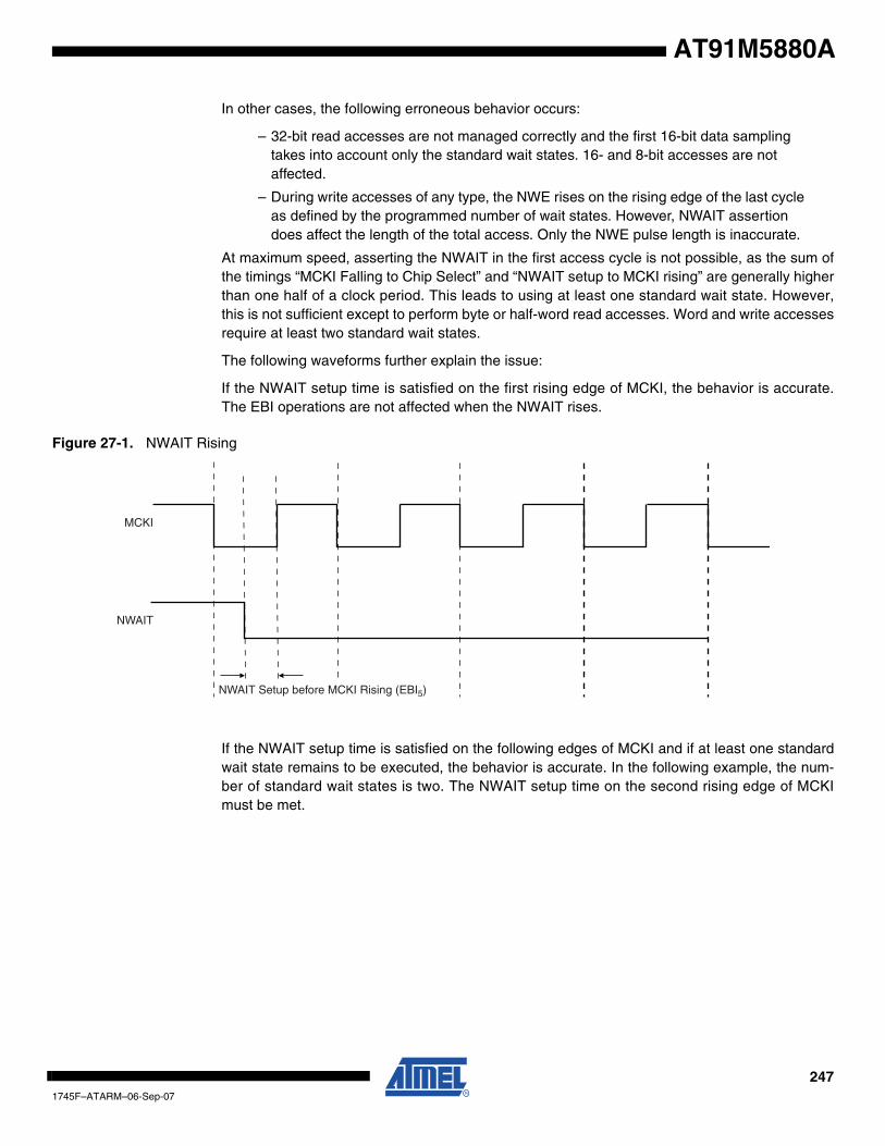
AT91M5880A
In other cases, the following erroneous behavior occurs:
– 32-bit read accesses are not managed correctly and the first 16-bit data sampling takes into account only the standard wait states. 16- and 8-bit accesses are not affected.
– During write accesses of any type, the NWE rises on the rising edge of the last cycle as defined by the programmed number of wait states. However, NWAIT assertion does affect the length of the total access. Only the NWE pulse length is inaccurate.
At maximum speed, asserting the NWAIT in the first access cycle is not possible, as the sum ofthe timings “MCKI Falling to Chip Select” and “NWAIT setup to MCKI rising” are generally higherthan one half of a clock period. This leads to using at least one standard wait state. However,this is not sufficient except to perform byte or half-word read accesses. Word and write accessesrequire at least two standard wait states.
The following waveforms further explain the issue:
If the NWAIT setup time is satisfied on the first rising edge of MCKI, the behavior is accurate.The EBI operations are not affected when the NWAIT rises.
Figure 27-1. NWAIT Rising
If the NWAIT setup time is satisfied on the following edges of MCKI and if at least one standardwait state remains to be executed, the behavior is accurate. In the following example, the num-ber of standard wait states is two. The NWAIT setup time on the second rising edge of MCKImust be met.
NWAIT Setup before MCKI Rising (EBI5)
MCKI
NWAIT
2471745F–ATARM–06-Sep-07

Figure 27-2. Number of Standard Wait States is Two
Note: 1. These numbers refer to the standard access cycles.
If the first two conditions are not met during a 32-bit read access, the first 16-bit data is read atthe end of the standard 16-bit read access. In the following example, the number of standardwaits is one. NWAIT assertions do affect both NRD pulse lengths, but first data sampling is notdelayed. The second data sampling is correct.
Figure 27-3. Number of Standard Wait States is One
Note: 1. These numbers refer to the standard access cycles.
Standard Access Length with Two Wait States
EBI5
1(1) 2(1) 3(1)
MCKI
NWAIT
NCS
32-bit Access = Two 16-bit AccessesEach Access Length = One Wait State + Assertion for One More Cycle
1(1) 2(1)
MCKI
NWAIT
NRD
2(1)
First Data Sampling(Erroneous)
1(1) 2(1)2(1)
Second Data Sampling(Correct)
EBI5
2481745F–ATARM–06-Sep-07
AT91M5880A

AT91M5880A
If the first two conditions are not met during write accesses, the NWE signal is not affected bythe NWAIT assertion. The following example illustrates the number of standard wait states.NWAIT is not asserted during the first cycle, but is asserted at the second and last cycle of thestandard access. The access is correctly delayed as the NCS line rises accordingly to theNWAIT assertion. However, the NWE signal waveform is unchanged, and rises too early.
Figure 27-4. Description of the Number of Standard Wait States
27.3 APMC: Unpredictable Result in APMC State Machine on Switch from Oscillator to PLLAn automatic switch from the main oscillator output (CSS = 1) may cause an unpredictableresult in the APMC state machine. The automatic PLL to PLL transition is also effected by thisproblem.
Problem Fix/WorkaroundThe user must either wait for the PLL lock flag to be set in the APMC status register or switch toan intermediate 32 kHz oscillator output (CSS = 0).
27.4 APMC: Clock Switching with the Prescaler in the APMC is not PermittedSwitching from the selected clock (PRES = 0) to the selected clock divided by 4 (PRES = 2), 8(PRES = 3) or 64 (PRES = 6) may lead to unpredictable results.
Problem Fix/Workaround First, the user should switch to any other value (PRES = 1, 4 or 5) and wait for the actual switchto perform (at least 64 cycles of the selected clock). Then, the user can write the final prescalervalue.
27.5 SPI: Initializing SPI in Master Mode May Cause a Mode Fault DetectionProblem Fix/Workaround
In order to prevent this error, the user must pull up the PA26/NPCS0/NSS pin to the VDDIO powersupply.
Access Length = One Wait State + Assertion of the NWAIT for One More Cycle
EBI5
MCKI
NWAIT
NWE
NCS
Erroneous NWE Rising
2491745F–ATARM–06-Sep-07

27.6 SPI: SPI in Slave Mode does not WorkIn transmission, the data to be transmitted (written in SP_TDR) is transferred in the shift registerand, consequently, the TDRE bit in SP_SR is set to 1. Though the transfer has not begun, whenthe following data are written in SP_TDR, they are also transferred into the shift register, crush-ing the precedent data and setting the bit TDRE to 1.
Problem Fix/WorkaroundNo problem fix/workaround to propose.
27.7 VDDBU Consumption is not GuaranteedThe battery supply voltage consumption is not guaranteed in the case of internal peripheralaccesses.
Problem Fix/WorkaroundThe user should minimally access the Advanced Peripheral Bus by using an interrupt-drivendriver rather than polling methods.
27.8 VDDCORE Current Consumption when PLL is not UsedIf the PLL is not used, an excessive current consumption can be seen on VDDPLL (about 2 mA).
Problem Fix/WorkaroundAt start-up, set the PLL on (set MUL at 2 and PLLCOUNT at 2, for example), wait for the PLLLOCK and then disable the PLL (MUL = 0).
2501745F–ATARM–06-Sep-07
AT91M5880A

AT91M5880A
Revision History.
Doc. Rev Date CommentsChange Request Ref.
1745A July, 2001 First Issue
1745B 18-Jul-2002
Page: 9 Change to Block Diagram.
Page: 9 “Peripherals”: Text changed.
Page 10 “User Peripherals”: Text changed.
Page: 16 “Internal Memories”: Text added to paragraph.
Page: 16 “Peripheral Data Controller”: Text changed.
Page: 18 “Digital-to-analog Converter”: Text changed.
Page: 204 “Digital-to-analog Converter”: Text changed.
Page: 205 “8- to 10-bit Conversion Mode”: Text changed.
1745C 16-Dec-2002
Page: 195 “Analog-to-Digitial Conversion”: Text removed.
Page: 199 PRESCAL: Text changed. Equation modified.
Page: 219 - 220 Table 25. bit 30 and bit 12 changed
1745D 03-Oct-2005
GlobalChange in format introduced Chapter numbering with change to table and figure numbering.
Package reference TQFP changed to LQFP
page 241
page 244
page 245
Section 24. ”Packaging Information”
Section 25. ”Soldering Profile”
Section 26. ”Ordering Information”
Chapters added to correspondwith Summary
page 14
page 246
Section 7.4.2 ”NTRST Pin” info addedFigure 7-1, “Separate or Common Reset Management,” added to chapterSection 27. ”Errata” added and previous dedicated errata document, lit° 1780, suppressed.
CSR 05-451
AT91 doc format update
1745E 18-Apr-2006
page 245 Section 26. ”Ordering Information”
AT91M55800A-33AI LQFP176 Sn/Pb package removedAT91M55800A-33CI BGA 176 Sn/Pb package removed
#2602
1745F 20-Aug-2007page 250 Section 27.8 ”VDDCORE Current Consumption when PLL is
not Used” added to Errata.
Updated template - page layout.
#4600
2511745F–ATARM–06-Sep-07

AT91M5880A
Table of Contents
Features ..................................................................................................... 1
1 Description ............................................................................................... 1
2 Pin Configurations ................................................................................... 3
3 Pin Description ......................................................................................... 7
4 Block Diagram .......................................................................................... 9
5 Architectural Overview .......................................................................... 10
5.1Memory ...................................................................................................................10
5.2Peripherals ..............................................................................................................10
6 Associated Documentation ................................................................... 12
7 Product Overview .................................................................................. 13
7.1Power Supplies .......................................................................................................13
7.2Input/Output Considerations ....................................................................................13
7.3Master Clock ...........................................................................................................14
7.4Reset .......................................................................................................................14
7.5Emulation Functions ................................................................................................15
7.6Memory Controller ...................................................................................................15
7.7External Bus Interface .............................................................................................17
8 Peripherals ............................................................................................. 18
8.1Peripheral Registers ................................................................................................18
8.2Peripheral Interrupt Control .....................................................................................18
8.3Peripheral Data Controller .......................................................................................18
8.4System Peripherals .................................................................................................19
8.5User Peripherals ......................................................................................................20
9 Memory Map ........................................................................................... 22
10 Peripheral Memory Map ........................................................................ 23
11 EBI: External Bus Interface ................................................................... 24
11.1External Memory Mapping ....................................................................................25
11.2EBI Pin Description ...............................................................................................26
11.3Data Bus Width .....................................................................................................27
11.4Byte-write or Byte-select Access ...........................................................................27
11.5Boot on NCS0 .......................................................................................................29
i1745F–ATARM–06-Sep-07

11.6Read Protocols ......................................................................................................30
11.7Write Data Hold Time ............................................................................................32
11.8Wait States ............................................................................................................33
11.9Memory Access Waveforms ..................................................................................36
11.10EBI User Interface ...............................................................................................48
12 APMC: Advanced Power Management Controller .............................. 52
12.1Operating Modes ...................................................................................................53
12.2Slow Clock Generator ...........................................................................................55
12.3Clock Generator ....................................................................................................56
12.4System Clock ........................................................................................................59
12.5Peripheral Clocks ..................................................................................................59
12.6Shut-down and Wake-up .......................................................................................59
12.7Alarm .....................................................................................................................60
12.8First Start-up Sequence ........................................................................................61
12.9APMC User Interface ............................................................................................62
13 RTC: Real-time Clock ............................................................................ 74
13.1Year 2000 Conformity ...........................................................................................74
13.2Functional Description ...........................................................................................75
13.3RTC User Interface ...............................................................................................77
14 WD: Watchdog Timer ............................................................................. 90
14.1WD User Interface .................................................................................................91
15 AIC: Advanced Interrupt Controller ..................................................... 96
15.1Hardware Interrupt Vectoring ................................................................................98
15.2Priority Controller ...................................................................................................98
15.3Interrupt Handling ..................................................................................................98
15.4Interrupt Masking ...................................................................................................99
15.5Interrupt Clearing and Setting ...............................................................................99
15.6Fast Interrupt Request ...........................................................................................99
15.7Software Interrupt ..................................................................................................99
15.8Spurious Interrupt ..................................................................................................99
15.9Protect Mode .......................................................................................................100
15.10AIC User Interface .............................................................................................102
15.11Standard Interrupt Sequence ............................................................................111
16 PIO: Parallel I/O Controller .................................................................. 113
ii1745F–ATARM–06-Sep-07
AT91M5880A
AT91M5880A
16.1Multiplexed I/O Lines ...........................................................................................113
16.2Output Selection ..................................................................................................113
16.3I/O Levels ............................................................................................................113
16.4Filters ...................................................................................................................113
16.5Interrupts .............................................................................................................114
16.6User Interface ......................................................................................................114
16.7Multi-driver (Open Drain) .....................................................................................114
16.8PIO Connection Tables ......................................................................................116
16.9PIO User Interface ...............................................................................................118
17 SF: Special Function Registers .......................................................... 129
17.1Chip Identifier ......................................................................................................129
17.2SF User Interface ................................................................................................129
18 USART: Universal Synchronous/ Asynchronous Receiver/Transmitter................................................................................................................ 134
18.1Pin Description ....................................................................................................135
18.2Baud Rate Generator ..........................................................................................136
18.3Receiver ..............................................................................................................137
18.4Transmitter ..........................................................................................................139
18.5Multi-drop Mode ..................................................................................................139
18.6Break ...................................................................................................................140
18.7Peripheral Data Controller ...................................................................................142
18.8Interrupt Generation ............................................................................................142
18.9Channel Modes ...................................................................................................142
18.10USART User Interface .......................................................................................144
19 TC: Timer Counter ............................................................................... 162
19.1Signal Name Description .....................................................................................164
19.2Timer Counter Description ..................................................................................165
19.3Capture Operating Mode .....................................................................................168
19.4Waveform Operating Mode .................................................................................170
19.5TC User Interface ................................................................................................173
20 SPI: Serial Peripheral Interface ........................................................... 190
20.1Pin Description ....................................................................................................190
20.2Master Mode .......................................................................................................191
20.3Slave Mode .........................................................................................................195
20.4Data Transfer ......................................................................................................196
iii1745F–ATARM–06-Sep-07

20.5Clock Generation .................................................................................................197
20.6Peripheral Data Controller ...................................................................................197
20.7SPI User Interface ...............................................................................................198
21 ADC: Analog-to-digital Converter ...................................................... 212
22 DAC: Digital-to-Analog Converter ...................................................... 224
22.1Conversion Details ..............................................................................................224
22.2DAC User Interface .............................................................................................226
23 JTAG Boundary-scan Register ........................................................... 233
24 Packaging Information ........................................................................ 241
25 Soldering Profile .................................................................................. 244
25.1LQFP Soldering Profile (Green) ..........................................................................244
25.2BGA Soldering Profile (RoHS-compliant) ............................................................244
26 Ordering Information .......................................................................... 245
27 Errata ..................................................................................................... 246
27.1ADC Characteristics and Behavior ......................................................................246
27.2Warning: Additional NWAIT Constraints ..............................................................246
27.3Unpredictable Result in APMC State Machine on Switch from Oscillator to PLL 249
27.4Clock Switching with the Prescaler in the APMC is not Permitted ......................249
27.5Initializing SPI in Master Mode May Cause a Mode Fault Detection ...................249
27.6SPI in Slave Mode does not Work .......................................................................250
27.7VDDBU Consumption is not Guaranteed ............................................................250
27.8VDDCORE Current Consumption when PLL is not Used ...................................250
Revision History.................................................................................... 251
Table of Contents....................................................................................... i
iv1745F–ATARM–06-Sep-07
AT91M5880A

Headquarters International
Atmel Corporation2325 Orchard ParkwaySan Jose, CA 95131USATel: 1(408) 441-0311Fax: 1(408) 487-2600
Atmel AsiaRoom 1219Chinachem Golden Plaza77 Mody Road TsimshatsuiEast KowloonHong KongTel: (852) 2721-9778Fax: (852) 2722-1369
Atmel EuropeLe Krebs8, Rue Jean-Pierre TimbaudBP 30978054 Saint-Quentin-en-Yvelines CedexFranceTel: (33) 1-30-60-70-00 Fax: (33) 1-30-60-71-11
Atmel Japan9F, Tonetsu Shinkawa Bldg.1-24-8 ShinkawaChuo-ku, Tokyo 104-0033JapanTel: (81) 3-3523-3551Fax: (81) 3-3523-7581
Product Contact
Web Sitewww.atmel.comwww.atmel.com/AT91SAM
Technical SupportAT91SAM SupportAtmel techincal support
Sales Contactswww.atmel.com/contacts/
Literature Requestswww.atmel.com/literature
Disclaimer: The information in this document is provided in connection with Atmel products. No license, express or implied, by estoppel or otherwise, to anyintellectual property right is granted by this document or in connection with the sale of Atmel products. EXCEPT AS SET FORTH IN ATMEL’S TERMS AND CONDI-TIONS OF SALE LOCATED ON ATMEL’S WEB SITE, ATMEL ASSUMES NO LIABILITY WHATSOEVER AND DISCLAIMS ANY EXPRESS, IMPLIED OR STATUTORYWARRANTY RELATING TO ITS PRODUCTS INCLUDING, BUT NOT LIMITED TO, THE IMPLIED WARRANTY OF MERCHANTABILITY, FITNESS FOR A PARTICULARPURPOSE, OR NON-INFRINGEMENT. IN NO EVENT SHALL ATMEL BE LIABLE FOR ANY DIRECT, INDIRECT, CONSEQUENTIAL, PUNITIVE, SPECIAL OR INCIDEN-TAL DAMAGES (INCLUDING, WITHOUT LIMITATION, DAMAGES FOR LOSS OF PROFITS, BUSINESS INTERRUPTION, OR LOSS OF INFORMATION) ARISING OUTOF THE USE OR INABILITY TO USE THIS DOCUMENT, EVEN IF ATMEL HAS BEEN ADVISED OF THE POSSIBILITY OF SUCH DAMAGES. Atmel makes norepresentations or warranties with respect to the accuracy or completeness of the contents of this document and reserves the right to make changes to specifica-tions and product descriptions at any time without notice. Atmel does not make any commitment to update the information contained herein. Unless specifically pro-vided otherwise, Atmel products are not suitable for, and shall not be used in, automotive applications. Atmel’s products are not intended, authorized, or warrantedfor use as components in applications intended to support or sustain life.
© 2007 Atmel Corporation. All rights reserved. Atmel®, logo and combinations thereof, and others are registered trademarks or trademarks ofAtmel Corporation or its subsidiaries. ARM®, the ARM Powered® logo and other are registered trademarks or trademarks of ARM Limited. Otherterms and product names may be trademarks of others.
1745F–ATARM–06-Sep-07


