
1.04-03222017-153500
USER MANUAL
COMe-9X90 Computer-On-Module Express

Copyright Copyright © 2013-2017 VIA Technologies Incorporated. All rights reserved.
No part of this document may be reproduced, transmitted, transcribed, stored in a retrieval system, or translated into any language,
in any form or by any means, electronic, mechanical, magnetic, optical, chemical, manual or otherwise without the prior written
permission of VIA Technologies, Incorporated.
Trademarks All trademarks are the property of their respective holders.
Disclaimer No license is granted, implied or otherwise, under any patent or patent rights of VIA Technologies. VIA Technologies makes no
warranties, implied or otherwise, in regard to this document and to the products described in this document. The information
provided in this document is believed to be accurate and reliable as of the publication date of this document. However, VIA
Technologies assumes no responsibility for the use or misuse of the information (including use or connection of extra
device/equipment/add-on card) in this document and for any patent infringements that may arise from the use of this document. The
information and product specifications within this document are subject to change at any time, without notice and without obligation
to notify any person of such change.
VIA Technologies, Inc. reserves the right the make changes to the products described in this manual at any time without prior notice.
Regulatory Compliance
FCC-A Radio Frequency Interference Statement This equipment has been tested and found to comply with the limits for a class A digital device, pursuant to part 15 of the FCC rules.
These limits are designed to provide reasonable protection against harmful interference when the equipment is operated in a
commercial environment. This equipment generates, uses, and can radiate radio frequency energy and, if not installed and used in
accordance with the instruction manual, may cause harmful interference to radio communications. Operation of this equipment in a
residential area is likely to cause harmful interference, in which case the user will be required to correct the interference at his
personal expense.
Notice 1 The changes or modifications not expressly approved by the party responsible for compliance could void the user's authority to
operate the equipment.
Notice 2 Shielded interface cables and A.C. power cord, if any, must be used in order to comply with the emission limits.
Notice 3 The product described in this document is designed for general use, VIA Technologies assumes no responsibility for the conflicts or
damages arising from incompatibility of the product. Check compatibility issue with your local sales representatives before placing
an order.
iii
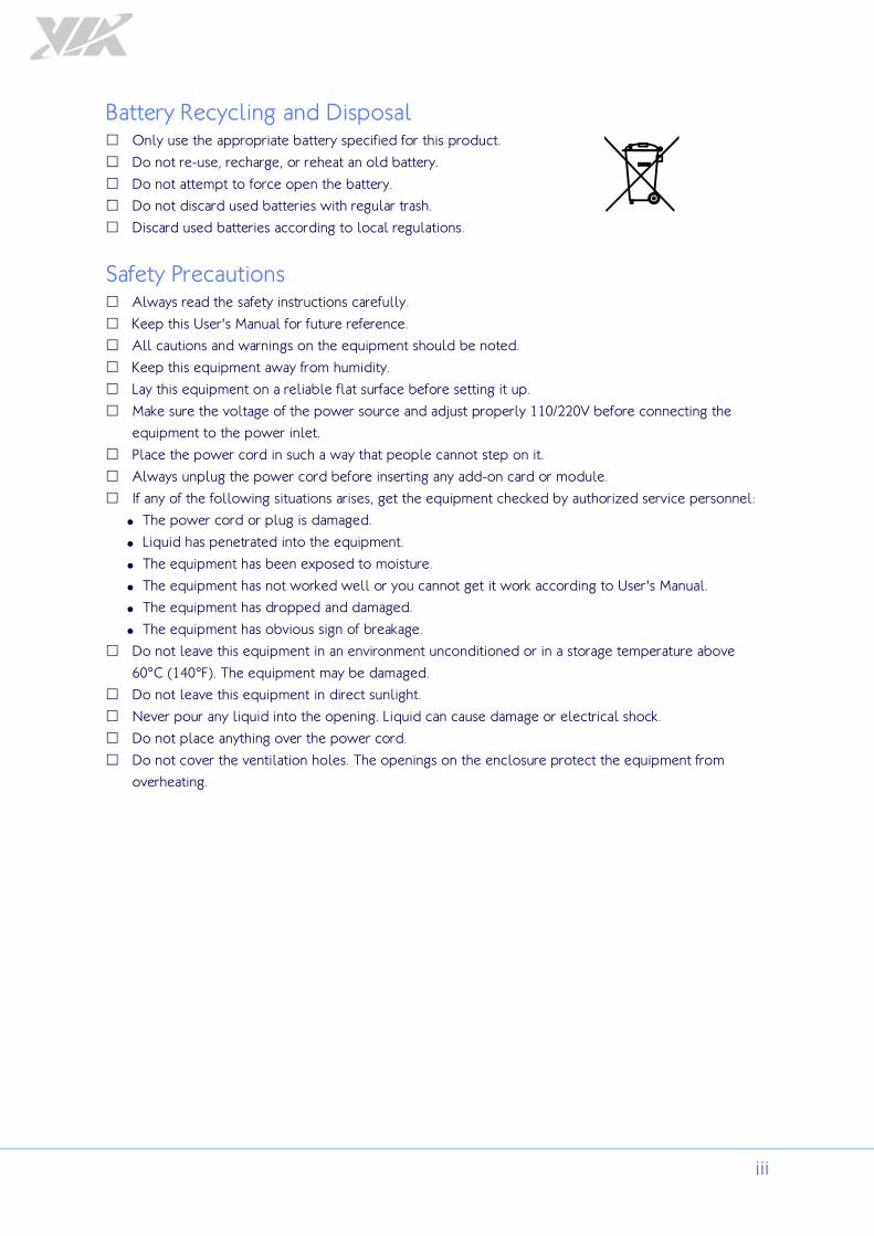
Battery Recycling and Disposal � Only use the appropriate battery specified for this product.
� Do not re-use, recharge, or reheat an old battery.
� Do not attempt to force open the battery.
� Do not discard used batteries with regular trash.
� Discard used batteries according to local regulations.
Safety Precautions � Always read the safety instructions carefully.
� Keep this User's Manual for future reference.
� All cautions and warnings on the equipment should be noted.
� Keep this equipment away from humidity.
� Lay this equipment on a reliable flat surface before setting it up.
� Make sure the voltage of the power source and adjust properly 110/220V before connecting the
equipment to the power inlet.
� Place the power cord in such a way that people cannot step on it.
� Always unplug the power cord before inserting any add-on card or module.
� If any of the following situations arises, get the equipment checked by authorized service personnel:
� The power cord or plug is damaged.
� Liquid has penetrated into the equipment.
� The equipment has been exposed to moisture.
� The equipment has not worked well or you cannot get it work according to User's Manual.
� The equipment has dropped and damaged.
� The equipment has obvious sign of breakage.
� Do not leave this equipment in an environment unconditioned or in a storage temperature above
60°C (140°F). The equipment may be damaged.
� Do not leave this equipment in direct sunlight.
� Never pour any liquid into the opening. Liquid can cause damage or electrical shock.
� Do not place anything over the power cord.
� Do not cover the ventilation holes. The openings on the enclosure protect the equipment from
overheating.

COMe-9X90 User Manual
iv
Box Contents
COMe-9X90 � 1 x COMe-9X90 module
� 1 x Screw bag
� 1 x Heatsink with fan (fansink)
Ordering Information Model Name Description
COMe-9X90 COM Express module with 1.2GHz VIA Nano® X2 E-Series CPU with 2 x
HDMI® or 2 x DisplayPort, VGA, LVDS, 2 x USB 3.0, 6 x USB 2.0, Gigabit
Ethernet, 2 x SATA, 4 x PCIe x1, ATX power connector
COMEDB4 COMe-9X90 evaluation carrier board
99G42-01380A Heatsink with fan for COMe-9X90
COMe-9X90 User Manual
v
Table of Contents
1. Product Overview ....................................................................................................................... 1
1.1. Key Components ............................................................................................................................................. 1
1.1.1. VIA Nano® X2 E-Series Processor .......................................................................................................... 1
1.1.2. VIA VX11 System Chipset ........................................................................................................................ 1
1.2. Product Specifications .................................................................................................................................... 2
1.3. Layout Diagram ................................................................................................................................................ 5
2. Hardware Installation ................................................................................................................. 6
2.1. CPU ..................................................................................................................................................................... 6
2.1.1. CPU Fan Connector: CPUFAN ................................................................................................................. 6
2.2. Memory Module Installation ........................................................................................................................ 7
2.2.1. Memory Slot: SODIMM ............................................................................................................................ 7
2.2.2. Installing the Memory ............................................................................................................................... 8
2.2.3. Removing a Memory Module .................................................................................................................. 8
2.3. Installing COMe-9X90 module to COMEDB4 carrier board .............................................................. 10
3. BIOS Setup Utility...................................................................................................................... 14
3.1. Entering the BIOS Setup Utility .................................................................................................................. 14
3.2. Control Keys ................................................................................................................................................... 14
3.3. Navigating the BIOS Menus......................................................................................................................... 14
3.4. Getting Help ................................................................................................................................................... 14
3.5. Main Menu....................................................................................................................................................... 15
3.5.1. BIOS Information ...................................................................................................................................... 15
3.5.2. Memory Information ................................................................................................................................ 15
3.5.3. System Language ...................................................................................................................................... 15
3.5.4. System Date ............................................................................................................................................... 15
3.5.5. System Time .............................................................................................................................................. 15
3.6. Advanced Settings ........................................................................................................................................ 16
3.6.1. ACPI Settings ............................................................................................................................................. 17
3.6.1.1. Enable Hibernation ....................................................................................................................... 17
3.6.1.2. ACPI Sleep State ............................................................................................................................ 17
3.6.2. S5 RTC Wake Settings ............................................................................................................................. 18
3.6.2.1. Wake system with Fixed Time .................................................................................................... 18
3.6.2.2. Wake system with Dynamic Time .............................................................................................. 18
3.6.3. CPU Information ....................................................................................................................................... 19
3.6.3.1. Enable PMON................................................................................................................................. 19
3.6.4. SATA Configuration ................................................................................................................................. 20
3.6.4.1. SATA Mode .................................................................................................................................... 20
3.6.5. USB Configuration .................................................................................................................................... 21
3.6.5.1. Legacy USB Support...................................................................................................................... 21
3.6.5.2. USB3.0 Support .............................................................................................................................. 21
3.6.5.3. XHCI Hand-off ................................................................................................................................ 21
3.6.5.4. EHCI Hand-off ................................................................................................................................ 22
3.6.5.5. USB Mass Storage Driver Support ............................................................................................. 22
COMe-9X90 User Manual
vi
3.6.5.6. USB transfer time-out .................................................................................................................... 22
3.6.5.7. Device reset time-out ................................................................................................................... 22
3.6.5.8. Device power-up delay ............................................................................................................... 22
3.6.6. F71869 Super IO Configuration ............................................................................................................ 23
3.6.6.1. Serial Port 0 Configuration .......................................................................................................... 23
3.6.6.1.1. Serial Port .................................................................................................................................. 23
3.6.6.2. Serial Port 1 Configuration .......................................................................................................... 23
3.6.6.2.1. Serial Port .................................................................................................................................. 23
3.6.6.3. Parallel Port Configuration .......................................................................................................... 23
3.6.6.3.1. Parallel Port .............................................................................................................................. 23
3.6.6.3.2. Change Settings ........................................................................................................................ 23
3.6.6.3.3. Device Mode ............................................................................................................................ 23
3.6.7. F71869 H/W Monitor............................................................................................................................... 24
3.6.8. F75308 H/W Monitor............................................................................................................................... 24
3.6.9. Clock Generator Configuration ............................................................................................................. 25
3.6.9.1. CPU Spread Spectrum .................................................................................................................. 25
3.6.9.2. PCIe Spread Spectrum .................................................................................................................. 25
3.6.10. Demo Board .............................................................................................................................................. 26
3.6.10.1. Backlight Control ........................................................................................................................... 26
3.6.10.2. Level ................................................................................................................................................. 26
3.7. Chipset Settings ............................................................................................................................................. 27
3.7.1. North Bridge .............................................................................................................................................. 28
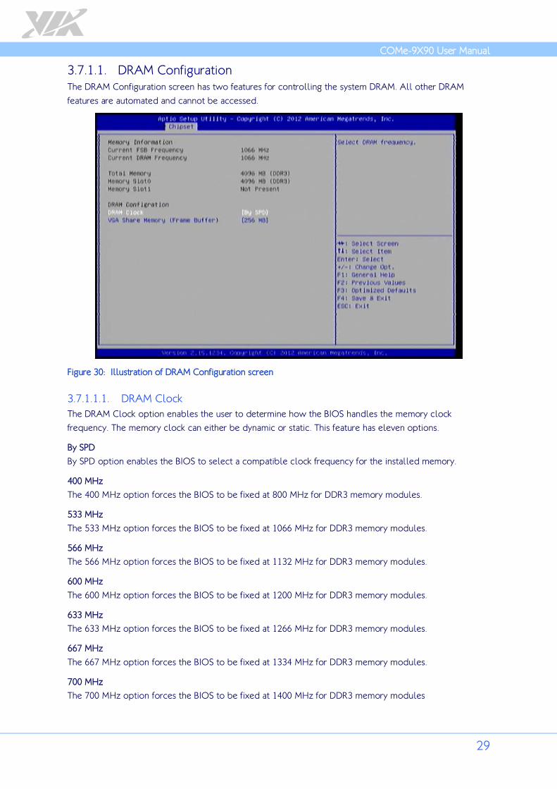
3.7.1.1. DRAM Configuration ..................................................................................................................... 29
3.7.1.1.1. DRAM Clock ............................................................................................................................. 29
3.7.1.1.2. VGA Share Memory (Frame Buffer) ..................................................................................... 30
3.7.1.2. Video Configuration ...................................................................................................................... 30
3.7.1.2.1. Select Display Device Control ............................................................................................. 30
3.7.1.2.2. Select Display Device 1 and 2 ............................................................................................. 30
3.7.1.2.3. Panel Type ................................................................................................................................. 31
3.7.2. South Bridge .............................................................................................................................................. 32
3.7.2.1. UART Configuration ...................................................................................................................... 33
3.7.2.1.1. PCI UART mode Selection ..................................................................................................... 33
3.7.2.1.2. UART 2 Enable ......................................................................................................................... 33
3.7.2.1.3. Io Base ........................................................................................................................................ 33
3.7.2.1.4. IRQ .............................................................................................................................................. 33
3.7.2.1.5. UART 3 Enable ......................................................................................................................... 33
3.7.2.1.6. Io Base ........................................................................................................................................ 33
3.7.2.1.7. IRQ .............................................................................................................................................. 33
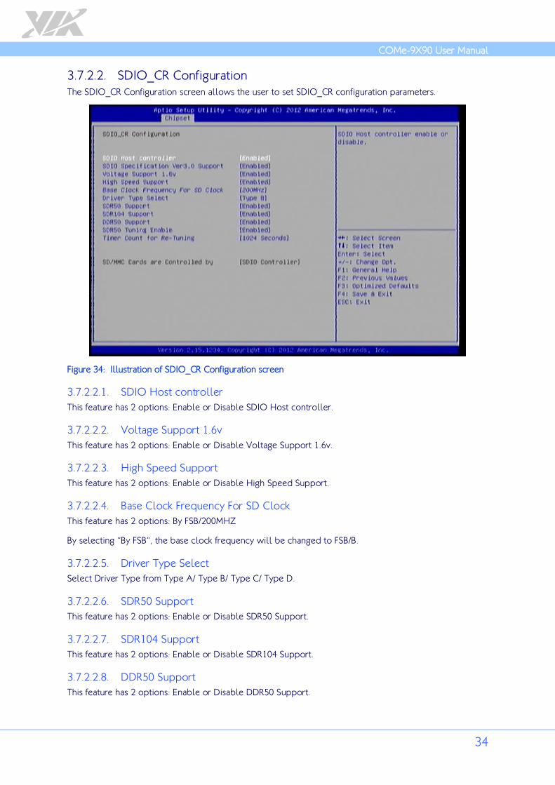
3.7.2.2. SDIO_CR Configuration................................................................................................................ 34
3.7.2.2.1. SDIO Host controller ............................................................................................................. 34
3.7.2.2.2. Voltage Support 1.6v .............................................................................................................. 34
3.7.2.2.3. High Speed Support ............................................................................................................... 34
3.7.2.2.4. Base Clock Frequency For SD Clock ................................................................................... 34
3.7.2.2.5. Driver Type Select ................................................................................................................... 34
3.7.2.2.6. SDR50 Support ......................................................................................................................... 34
3.7.2.2.7. SDR104 Support ....................................................................................................................... 34
3.7.2.2.8. DDR50 Support ........................................................................................................................ 34
COMe-9X90 User Manual
vii
3.7.2.2.9. SDR50 Tuning Enable ............................................................................................................. 35
3.7.2.2.10. Timer Count for Re-Tuning .................................................................................................. 35
3.7.2.3. PMU_ACPI Configuration ............................................................................................................. 36
3.7.2.3.1. Other Control ........................................................................................................................... 36
3.7.2.3.1.1. AC Loss Auto-restart ...................................................................................................... 37
3.7.2.3.1.2. USB S4 WakeUp .............................................................................................................. 37
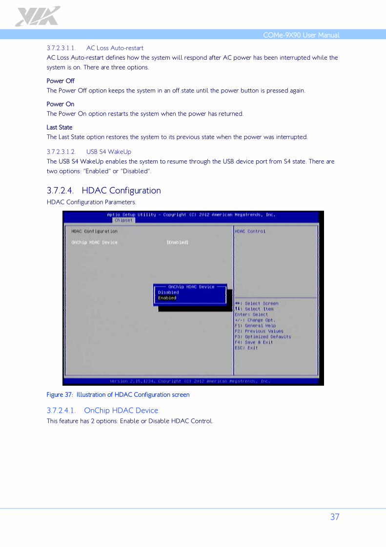
3.7.2.4. HDAC Configuration ..................................................................................................................... 37
3.7.2.4.1. OnChip HDAC Device............................................................................................................ 37
3.7.2.5. Others Configuration .................................................................................................................... 38
3.7.2.5.1. WATCHDOG Timer Enable .................................................................................................. 38
3.8. Boot Settings .................................................................................................................................................. 39
3.8.1. Boot Configuration ................................................................................................................................... 39
3.8.1.1. Setup Prompt Timeout ................................................................................................................. 39
3.8.1.2. BootupNumLock State .................................................................................................................. 39
3.8.1.3. Display Logo ................................................................................................................................... 39
3.8.1.4. Fast Boot .......................................................................................................................................... 39
3.8.2. Boot Option Priorities ............................................................................................................................. 40
3.8.2.1. Boot Option #1 .............................................................................................................................. 40
3.8.3. Network Device BBS Priorities .............................................................................................................. 40
3.8.3.1. Boot Option #1 .............................................................................................................................. 40
3.8.4. CSM parameters ....................................................................................................................................... 40
3.8.4.1. Launch CSM .................................................................................................................................... 40
3.8.4.2. Boot option filter ........................................................................................................................... 40
3.8.4.3. Launch PXE OpROM policy ........................................................................................................ 40
3.8.4.4. Launch Storage OpROM policy ................................................................................................. 40
3.8.4.5. Launch Video OpROM policy .................................................................................................... 40
3.8.4.6. Other PCI device ROM priority .................................................................................................. 40
3.9. Security Settings............................................................................................................................................. 41
3.9.1. Security Settings ....................................................................................................................................... 41
3.9.1.1. Administrator Password / User Password ................................................................................ 41
3.9.1.2. Password Check ............................................................................................................................. 41
3.10. Save & Exit Options ...................................................................................................................................... 42
3.10.1. Save Changes and Exit ............................................................................................................................ 42
3.10.2. Discard Changes and Exit ....................................................................................................................... 42
3.10.3. Save Changes and Reset ......................................................................................................................... 42
3.10.4. Discard Changes and Reset .................................................................................................................... 42
3.10.5. Save Changes ............................................................................................................................................ 43
3.10.6. Discard Changes ....................................................................................................................................... 43
3.10.7. Save as User Defaults .............................................................................................................................. 43
3.10.8. Restore User Defaults .............................................................................................................................. 43
3.10.9. Realtek PXE B01 D00............................................................................................................................... 43
4. Driver Installation ...................................................................................................................... 44
4.1. Microsoft Driver Support ............................................................................................................................. 44
4.2. Linux Driver Support ..................................................................................................................................... 44

COMe-9X90 User Manual
viii
Appendix A. COMEDB4 Carrier Board ......................................................................................... 45
A.1. Board Specifications.............................................................................................................................................. 45
A.2. External I/O Connectors ...................................................................................................................................... 47
A.2.1. Front Panel I/O ............................................................................................................................................... 47
A.2.2. Rear Panel I/O ................................................................................................................................................. 47
A.3. COMEDB4 Layout Diagram ................................................................................................................................. 48
A.3.1. Onboard Slots, Buttons and Power Connectors .................................................................................... 48
A.3.2. Onboard Pin headers and Connectors ..................................................................................................... 49
A.3.2.1. Pin Headers and Connectors Pin Definition .................................................................................. 51
A.3.3. Onboard Jumpers .......................................................................................................................................... 57
A.3.3.1. Jumper Settings .................................................................................................................................... 58

COMe-9X90 User Manual
ix
List of Figures Figure 1: Layout diagram of the COMe-9X90 module (top view) ...........................................................................5
Figure 2: Layout diagram of the COMe-9X90 module (bottom view) ....................................................................5
Figure 3: CPU with heatsink and fan .................................................................................................................................6
Figure 4: CPU fan connector diagram ..............................................................................................................................6
Figure 5: DDR3 SODIMM1 slot diagram (top side) ......................................................................................................7
Figure 6: DDR3 SODIMM2 slot diagram (bottom side) ..............................................................................................7
Figure 7: Inserting the memory module ..........................................................................................................................8
Figure 8: Locking the memory module ...........................................................................................................................8
Figure 9: Disengaging the SODIMM locking clips ........................................................................................................8
Figure 10: Removing the memory module .....................................................................................................................9
Figure 11: Carrier board mounting points and connectors ..................................................................................... 10
Figure 12: Installing carrier board hex spacers .......................................................................................................... 11
Figure 13: Installing COMe-9X90 module .................................................................................................................. 12
Figure 14: Securing the COMe-9X90 module and applying the thermal paste ................................................. 12
Figure 15: Installing and securing the heatsink ........................................................................................................... 13
Figure 16: Illustration of the Main menu screen ......................................................................................................... 15
Figure 17: Illustration of the Advanced Settings screen .......................................................................................... 16
Figure 18: Illustration of the ACPI Settings screen .................................................................................................... 17
Figure 19: Illustration of S5 RTC Wake Settings screen............................................................................................ 18
Figure 20: Illustration of CPU Information screen ...................................................................................................... 19
Figure 21: Illustration of SATA Configuration screen ............................................................................................... 20
Figure 22: Illustration of USB Configuration screen .................................................................................................. 21
Figure 23: Illustration of F71869 Super IO Configuration screen ........................................................................... 23
Figure 24: Illustration of F71869 H/W Monitor screen ............................................................................................. 24
Figure 25: Illustration of F75308 H/W Monitor screen ............................................................................................. 24
Figure 26: Illustration of Clock Generator Configuration screen ........................................................................... 25
Figure 27: Illustration of Demo Board screen ............................................................................................................. 26
Figure 28: Illustration of Chipset Settings screen ...................................................................................................... 27
Figure 29: Illustration of North Bridge screen ............................................................................................................ 28
Figure 30: Illustration of DRAM Configuration screen .............................................................................................. 29
Figure 31: Illustration of Video Configuration screen ............................................................................................... 30
Figure 32: Illustration of South Bridge screen ............................................................................................................ 32
Figure 33: Illustration of UART Configuration screen ............................................................................................... 33
Figure 34: Illustration of SDIO_CR Configuration screen......................................................................................... 34
Figure 35: Illustration of PMU_ACPI Configuration screen ...................................................................................... 36
Figure 36: Illustration of Other Control screen .......................................................................................................... 36
Figure 37: Illustration of HDAC Configuration screen .............................................................................................. 37
Figure 38: Illustration of Others Configuration screen ............................................................................................. 38
Figure 39: Illustration of Boot Settings screen ............................................................................................................ 39
Figure 40: Illustration of Security Settings screen ...................................................................................................... 41
Figure 41: Illustration of Save & Exit Options screen ............................................................................................... 42
Figure 42: Front panel I/O ............................................................................................................................................... 47
Figure 43: Rear panel IO .................................................................................................................................................. 47
Figure 44: COMEDB4 slots, buttons, and power connectors layout .................................................................... 48
Figure 45: COMEDB4 pin headers and connectors layout ...................................................................................... 49
Figure 46: COMEDB4 jumpers layout ........................................................................................................................... 57

COMe-9X90 User Manual
x
List of Tables
Table 1: CPU fan connector pinout .................................................................................................................................6
Table 2: Layout diagram description table of the COMEDB4 (pin headers and connectors) ........................ 50
Table 3: Layout diagram description table of the COMEDB4 (jumpers) ............................................................. 57

COMe-9X90 User Manual
1
1. Product Overview The VIA COMe-9X90 is a compact and highly integrated COM Express module. It comes with an
integrated 1.2GHz VIA Nano® X2 E-Series (or 1.0GHz VIA QuadCore E-Series) processor, boasting of
ultra-low power consumption, cool and quiet operation, and enhanced multi-tasking ability.
The COMe-9X90 is based on the VIA VX11 chipset featuring the Integrated VIA C-640/645 DirectX11
graphics processor and unified video decoding accelerator that offers rich visual and 3D/2D contents for
immersive environments. It provides support for extensive connectivity options, including audio, USB,
DisplayPort, COM port, Ethernet, and graphics, through board-to-board connectors to an I/O carrier
board.
1.1. Key Components
1.1.1. VIA Nano® X2 E-Series Processor The VIA Nano® X2 E-Series is a dual-core processor and 64-bit superscalar processor in x86 platform
using a 40 nanometer process technology. It delivers an energy-efficient, powerful performance, with cool
and quiet operation all within an ultra-compact NanoBGA2 package measuring 21mm x 21mm.
VIA Nano® X2 E-Series processor offers an excellent performance on multitasking application that makes
it perfect for embedded system applications such as industrial PCs, test machines, measuring equipment,
digital signage, medical PCs, monitoring systems, gaming machines, in-vehicle entertainment, and etc. The
VIA Nano® X2 E-Series processor also boasts of immersive multimedia performance, connectivity and
computing applications
1.1.2. VIA VX11 System Chipset The VIA VX11 is the fourth generation, highly integrated Media System Processor which provides high
quality digital video streaming and high definition video playback. It features the VIA C- 640/645 DX11
3D/2D graphics and video processor, High Definition video decoder supports DDR3 1333 controller and
USB 3.0 interface.
The VIA VX11 offers superb-graphics performance, immersive visual experience, and supports DirectX
11.0 that allows realistic 3D rendering and increased visual acuity. The VIA VX11 is based on a highly
sophisticated power efficient architecture that enables such rich integration into a compact package.
COMe-9X90 User Manual
2
1.2. Product Specifications
Core Processor
1.2GHz VIA Nano® X2 E-Series processor
1MB L2 Cache
1066MHz FSB
1.0GHz VIA QuadCore E-Series processor (manufacturing option)
1MB L2 Cache
800MHz FSB
Chipset
VIA VX11 Media System Processor
System Memory
2 x DDR3 1333/1066 SODIMM slots
Supports up to 16GB memory size
BIOS
AMI eEFI BIOS,
32Mbit SPI flash memory
Operating System
Windows 7
Windows XP
Windows XPe
Windows Embedded System 7
Windows CE6.0
Linux
Hardware Monitoring
CPU temperature reading
CPU fan speed reading
System voltage monitoring
Expansion Bus
4 x PCIe x1
System Monitoring and Management
Wake-on-LAN
System power management
AC power failure recovery
Watchdog Timer (software programmable)

COMe-9X90 User Manual
3
Video Graphics processor
Integrated VIA C-645/640 DX11 3D/2D graphics with MPEG-2, VC1 and
H.264 video decoding acceleration
Graphics memory
Optimized Unified Memory Architecture (UMA) supports frame buffer
size from 64MB to 1GB (BIOS)
CRT Interface
1 x Analog VGA port supports up to 2048 x 1536 resolution
LVDS Interface
1 x LVDS channel supports dual-channel 18-bit or 24-bit LVDS panel
(VIA VT1636 or Chrontel CH7305)
DisplayPort Interface
DisplayPort 1 : Supports DisplayPort/HDMI® interface
DisplayPort 2 : Supports DisplayPort/HDMI® interface
Audio Controller
VT2021 High Definition Audio Codec
Ethernet Controller
Realtek RTL8111G/GS 10/100/1000M PCIe Gigabit Ethernet controller
Input/Output Audio
Supports 1 High Definition audio digital interface
LAN
Supports 1 Gigabit Ethernet port
USB
Supports up to 2 USB 3.0 ports
Supports up to 6 USB 2.0 ports
SATA
Supports up to 2 SATA 3.0 Gbps ports
Serial
Supports 2 serial ports with TX and RX signal
COMe-9X90 User Manual
4
DisplayPort
Supports 2 DisplayPort
Expansion Buses
Supports 1 SMBus interface
Supports 1 I2C bus
Supports 1 SDIO interface as default (shared with GPIO 4 INs and 4
OUTs)
Supports 1 LPC bus interface
Supports SPI
Supports ExpressCard, speaker out, reset function, thermal protection,
suspend/wake signals, power button, and fan control signals
Mechanical
and
Environment
COM Express Compliance
COM Express™ Type 6, Basic Module
Dimension
95mm x 125mm (3.73” x4.92”)
Operating Temperature
0˚C ~ 60˚C
Storage Temperature
-40˚C ~ 70˚C
Operating Humidity
0% ~ 95% (relative humidity; non-condensing)
Compliance
CE
FCC
BSMI
RoHS
Note:
As the operating temperature provided in the specifications is a result of the test performed in VIA’s chamber, a
number of variables can influence this result. Please note that the working temperature may vary depending on
the actual situation and environment. It is highly suggested to execute a solid testing and take all the variables
into consideration when building the system. Please ensure that the system runs well under the operating
temperature in terms of application.

COMe-9X90 User Manual
5
1.3. Layout Diagram
DDR3 SODIMM slot 1
VIA Nano X2 E-Series CPU
CPU fan connector
VIA VX11 Chipset
Figure 1: Layout diagram of the COMe-9X90 module (top view)
A1
B1
C1
D1
Pin Connector B
Pin Connector A
DDR3 SODIMM slot 2
Figure 2: Layout diagram of the COMe-9X90 module (bottom view)
COMe-9X90 User Manual
6
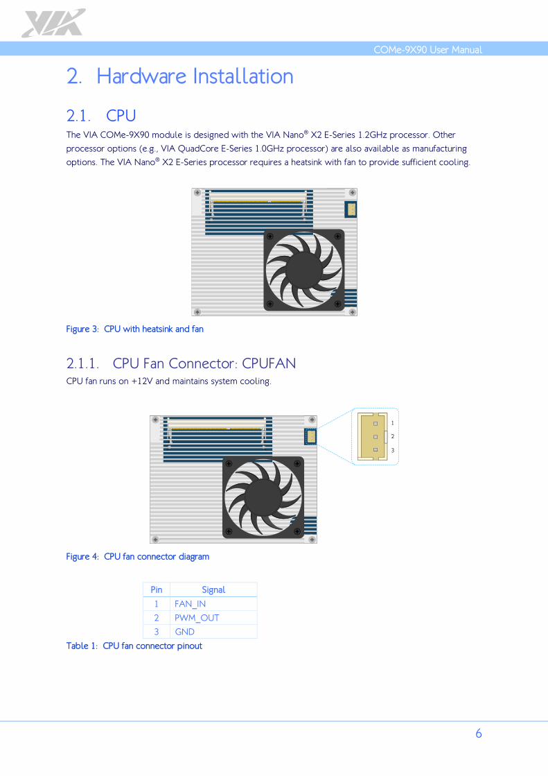
2. Hardware Installation
2.1. CPU The VIA COMe-9X90 module is designed with the VIA Nano® X2 E-Series 1.2GHz processor. Other
processor options (e.g., VIA QuadCore E-Series 1.0GHz processor) are also available as manufacturing
options. The VIA Nano® X2 E-Series processor requires a heatsink with fan to provide sufficient cooling.
Figure 3: CPU with heatsink and fan
2.1.1. CPU Fan Connector: CPUFAN CPU fan runs on +12V and maintains system cooling.
Figure 4: CPU fan connector diagram
Pin Signal
1 FAN_IN
2 PWM_OUT
3 GND
Table 1: CPU fan connector pinout
COMe-9X90 User Manual
7
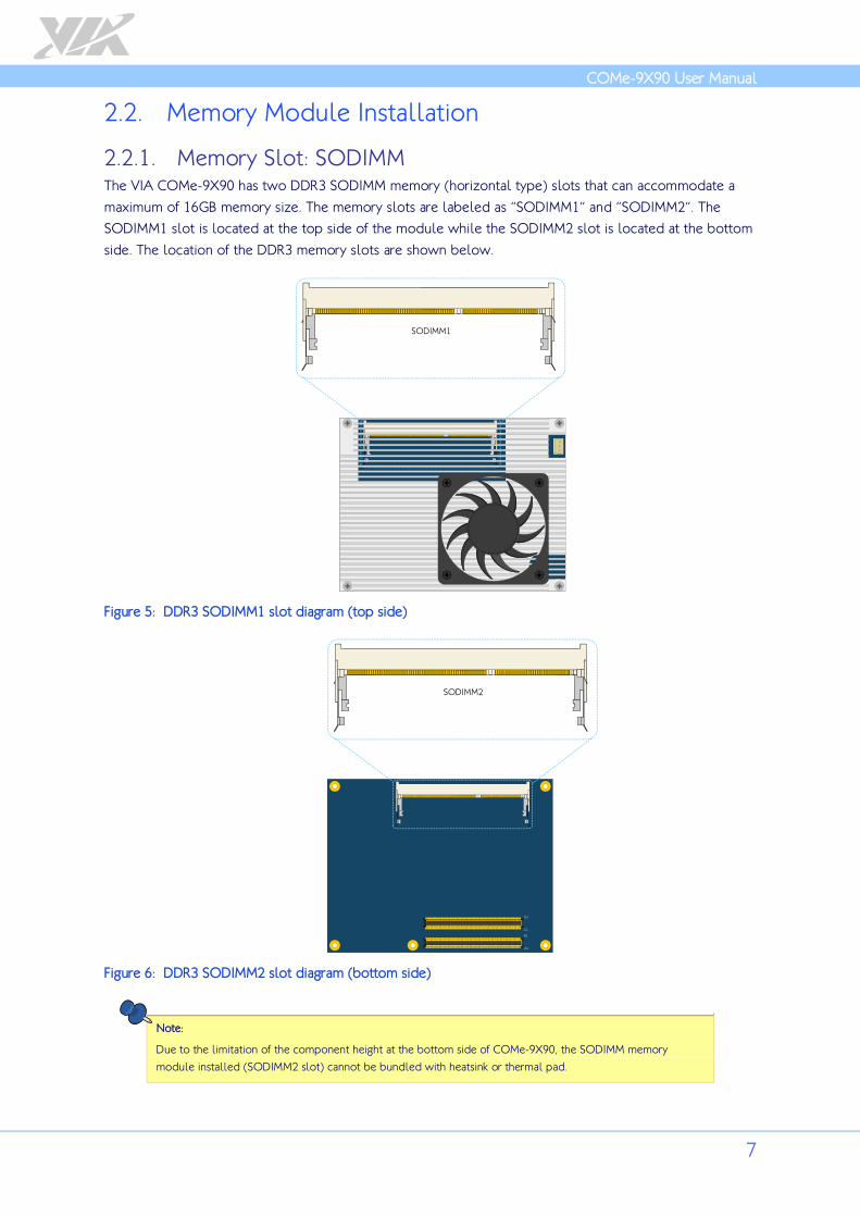
2.2. Memory Module Installation
2.2.1. Memory Slot: SODIMM The VIA COMe-9X90 has two DDR3 SODIMM memory (horizontal type) slots that can accommodate a
maximum of 16GB memory size. The memory slots are labeled as “SODIMM1” and “SODIMM2”. The
SODIMM1 slot is located at the top side of the module while the SODIMM2 slot is located at the bottom
side. The location of the DDR3 memory slots are shown below.
Figure 5: DDR3 SODIMM1 slot diagram (top side)
Figure 6: DDR3 SODIMM2 slot diagram (bottom side)
Note:
Due to the limitation of the component height at the bottom side of COMe-9X90, the SODIMM memory
module installed (SODIMM2 slot) cannot be bundled with heatsink or thermal pad.

COMe-9X90 User Manual
8
2.2.2. Installing the Memory
Step 1
Align the notch on the memory module with the protruding wedge on the SODIMM slot. Insert the
memory module into the slot at 30 degrees angle.
Figure 7: Inserting the memory module
Step 2
Push down until the memory module snaps into place. The memory slot has two locking mechanisms that
will click once the memory module has been fully inserted.
Figure 8: Locking the memory module
2.2.3. Removing a Memory Module
Step 1
Disengage the locking clasps at both ends of the memory slot.
Figure 9: Disengaging the SODIMM locking clips
COMe-9X90 User Manual
9
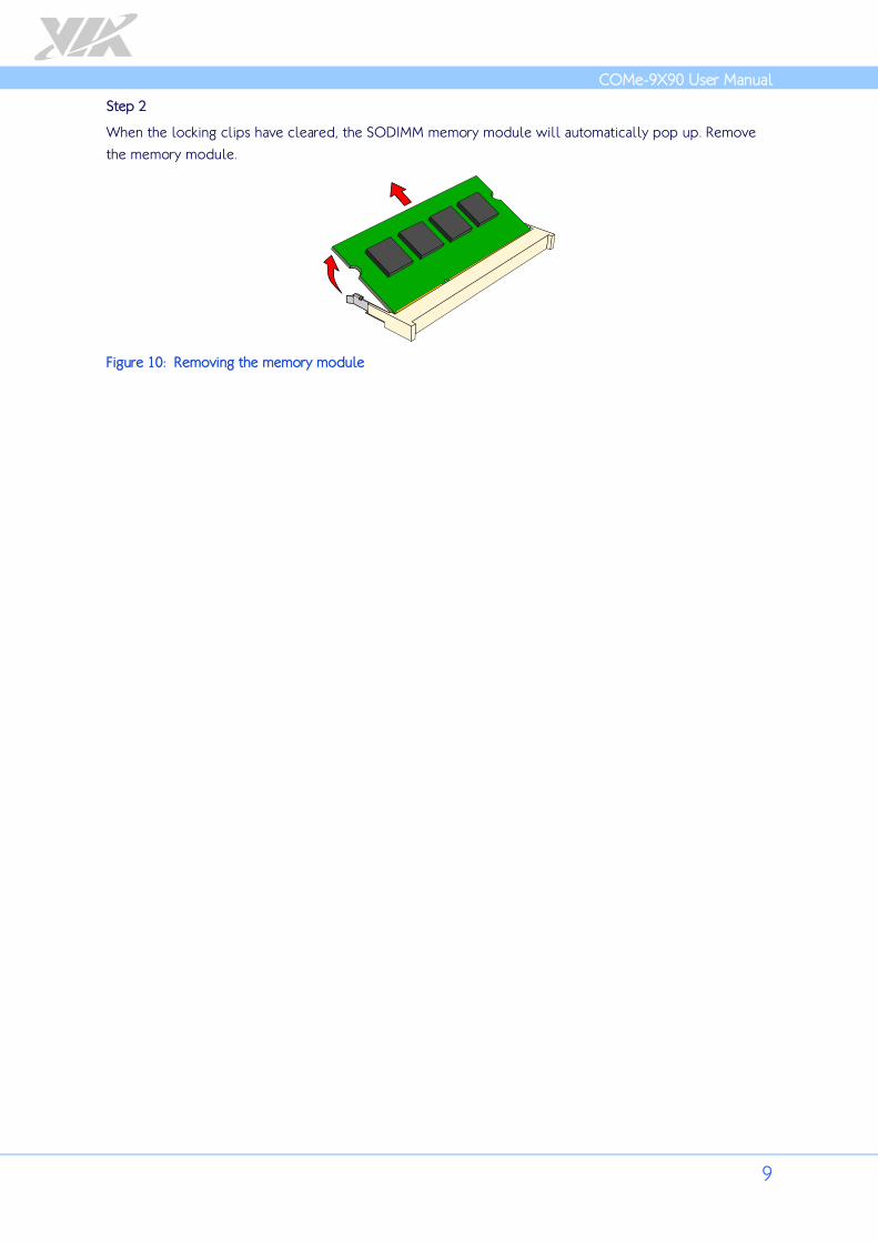
Step 2
When the locking clips have cleared, the SODIMM memory module will automatically pop up. Remove
the memory module.
Figure 10: Removing the memory module
COMe-9X90 User Manual
10
2.3. Installing COMe-9X90 module to COMEDB4 carrier
board
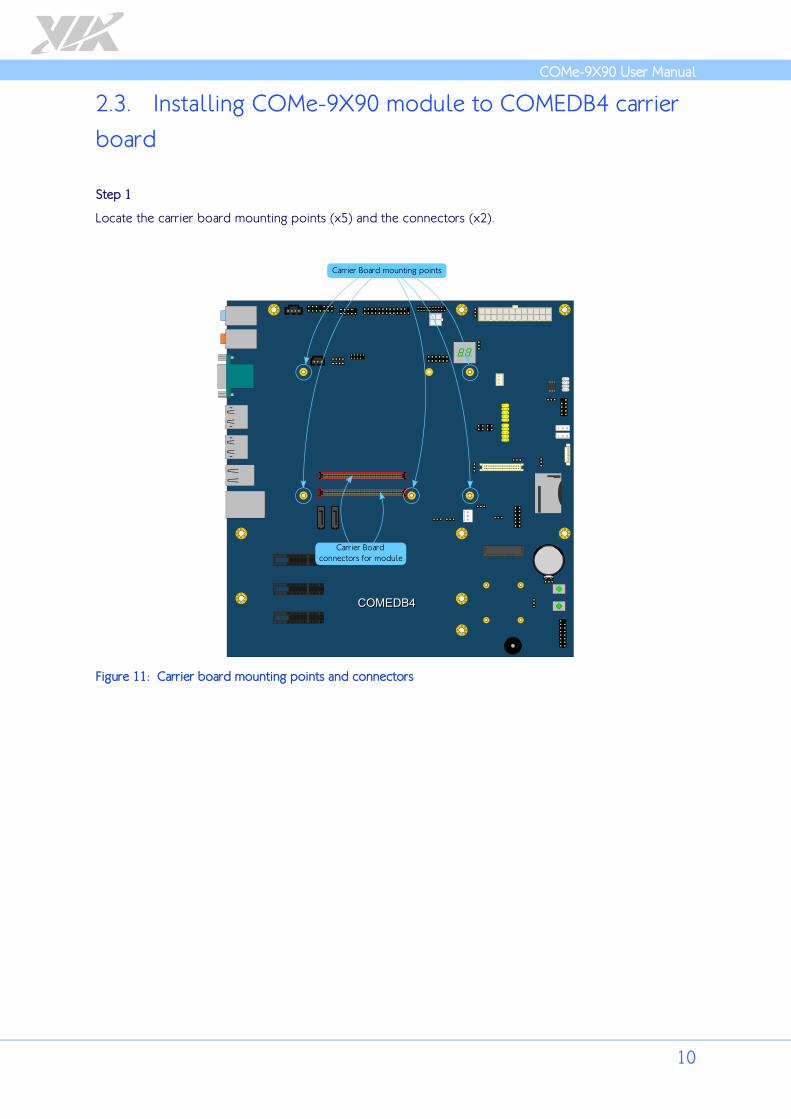
Step 1
Locate the carrier board mounting points (x5) and the connectors (x2).
Figure 11: Carrier board mounting points and connectors

COMe-9X90 User Manual
11
Step 2
Install five hex spacers onto the carrier board. The hex spacers must be placed on top of the board. From
the bottom of the board, tighten the hex spacers by using the M2.5x4mm screws (x5).
Figure 12: Installing carrier board hex spacers
COMe-9X90 User Manual
12
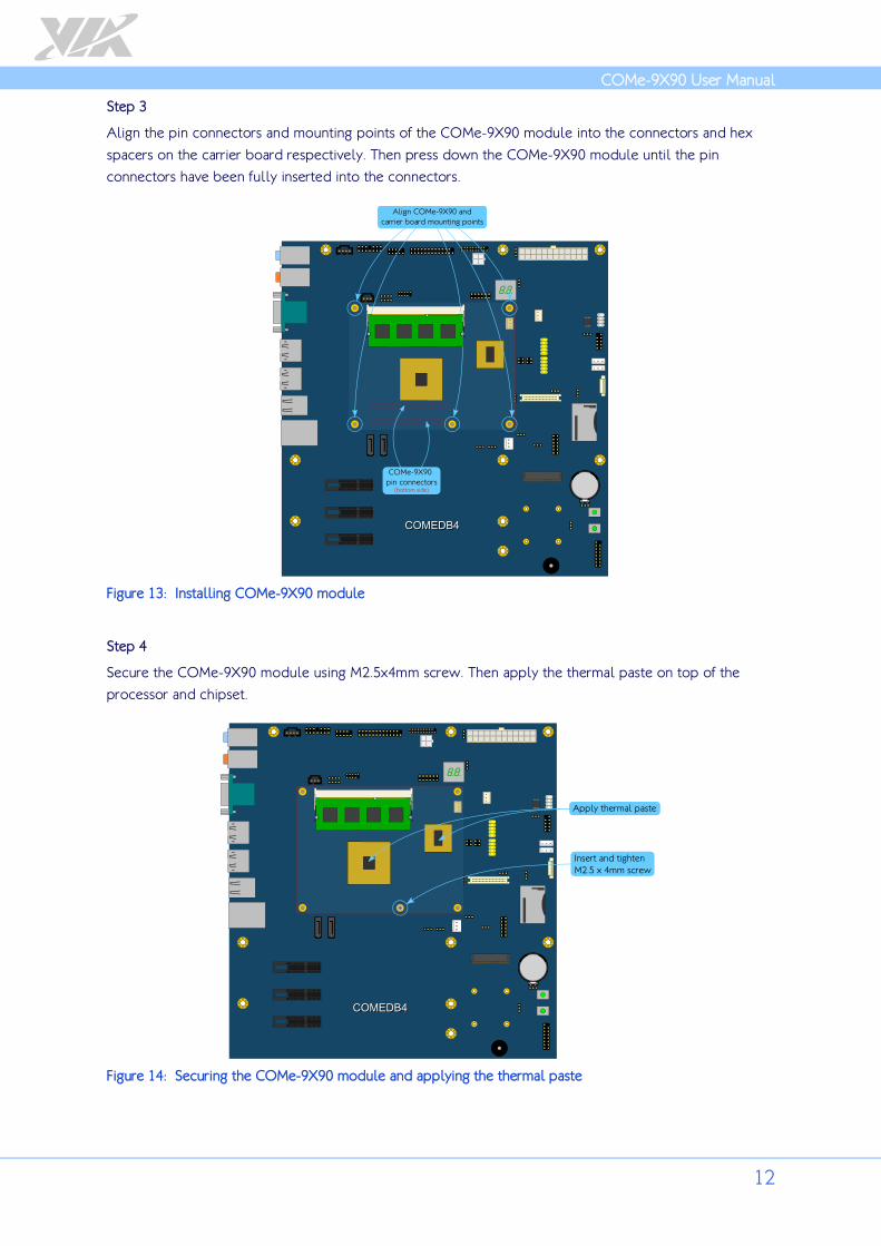
Step 3
Align the pin connectors and mounting points of the COMe-9X90 module into the connectors and hex
spacers on the carrier board respectively. Then press down the COMe-9X90 module until the pin
connectors have been fully inserted into the connectors.
Figure 13: Installing COMe-9X90 module
Step 4
Secure the COMe-9X90 module using M2.5x4mm screw. Then apply the thermal paste on top of the
processor and chipset.
Figure 14: Securing the COMe-9X90 module and applying the thermal paste

COMe-9X90 User Manual
13
Step 5
Install the heatsink on COMe-9X90 module. Secure it with four M2.5x15mm screws (with 3mm plastic
washer).
Figure 15: Installing and securing the heatsink
Step 6
Connect the CPU fan connector cable.
COMe-9X90 User Manual
14
3. BIOS Setup Utility
3.1. Entering the BIOS Setup Utility Power on the computer and press Delete during the beginning of the boot sequence to enter the BIOS
Setup Utility. If the entry point has passed, restart the system and try again.
3.2. Control Keys Up Move up one row
Down Move down one row
Left Move to the left in the navigation bar
Right Move to the right in the navigation bar
Enter Access the highlighted item / Select the item
Esc Jumps to the Exit screen or returns to the previous screen
Page up / +1 Increase the numeric value
Page down / -1 Decrease the numeric value
F1 General help2
F2 Restore the previous CMOS value
F3 Load optimized defaults
F4 Save all the changes and exit
Notes:
1. Must be pressed using the 10-key pad.
2. The General help contents are only for the Status Page and Option Page setup menus.
3.3. Navigating the BIOS Menus The main menu displays all the BIOS setup categories. Use the <Left>/<Right> and <Up>/<Down> arrow
keys to select any item or sub-menu. Descriptions of the selected/highlighted category are displayed at
the bottom of the screen.
The small triangular arrowhead symbol next to a field indicates that a sub-menu is available (see figure
below). Press <Enter> to display the sub-menu. To exit the sub-menu, press <Esc>.
3.4. Getting Help The BIOS Setup Utility provides a “General Help” screen. This screen can be accessed at any time by
pressing F1. The help screen displays the keys for using and navigating the BIOS Setup Utility. Press Esc to
exit the help screen.
COMe-9X90 User Manual
15
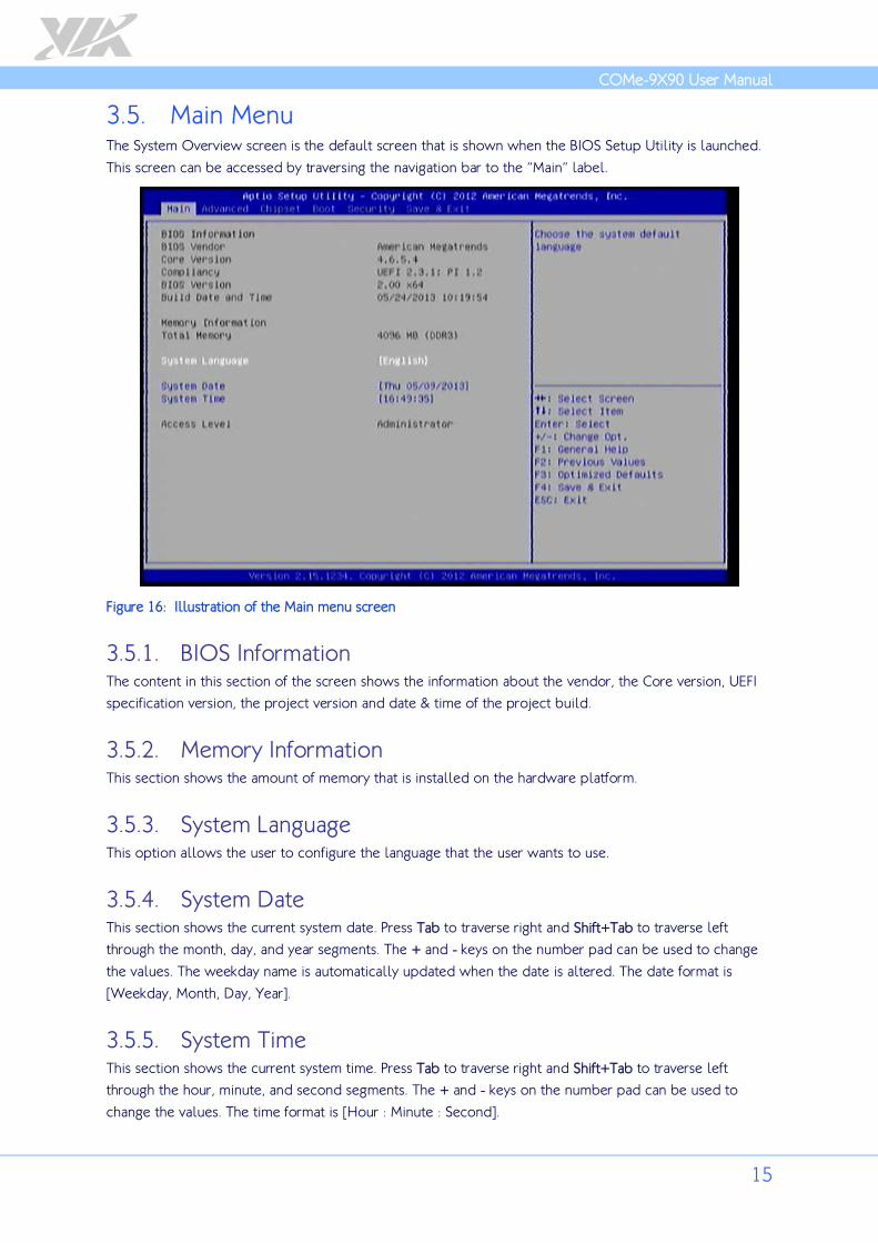
3.5. Main Menu The System Overview screen is the default screen that is shown when the BIOS Setup Utility is launched.
This screen can be accessed by traversing the navigation bar to the “Main” label.
Figure 16: Illustration of the Main menu screen
3.5.1. BIOS Information The content in this section of the screen shows the information about the vendor, the Core version, UEFI
specification version, the project version and date & time of the project build.
3.5.2. Memory Information This section shows the amount of memory that is installed on the hardware platform.
3.5.3. System Language This option allows the user to configure the language that the user wants to use.
3.5.4. System Date This section shows the current system date. Press Tab to traverse right and Shift+Tab to traverse left
through the month, day, and year segments. The + and - keys on the number pad can be used to change
the values. The weekday name is automatically updated when the date is altered. The date format is
[Weekday, Month, Day, Year].
3.5.5. System Time This section shows the current system time. Press Tab to traverse right and Shift+Tab to traverse left
through the hour, minute, and second segments. The + and - keys on the number pad can be used to
change the values. The time format is [Hour : Minute : Second].

COMe-9X90 User Manual
16
3.6. Advanced Settings The Advanced Settings screen shows a list of categories that can provide access to a sub-screen. Sub-
screen links can be identified by the preceding right-facing arrowhead.
Figure 17: Illustration of the Advanced Settings screen
The Advanced Settings screen contains the following links:
• ACPI Settings
• S5 RTC Wake Settings
• CPU Information
• SATA Configuration
• USB Configuration
• F71869 Super IO Configuration
• F71869 H/W Monitor
• F75308 HW Monitor
• Clock Generator Configuration
• Demo Board
COMe-9X90 User Manual
17
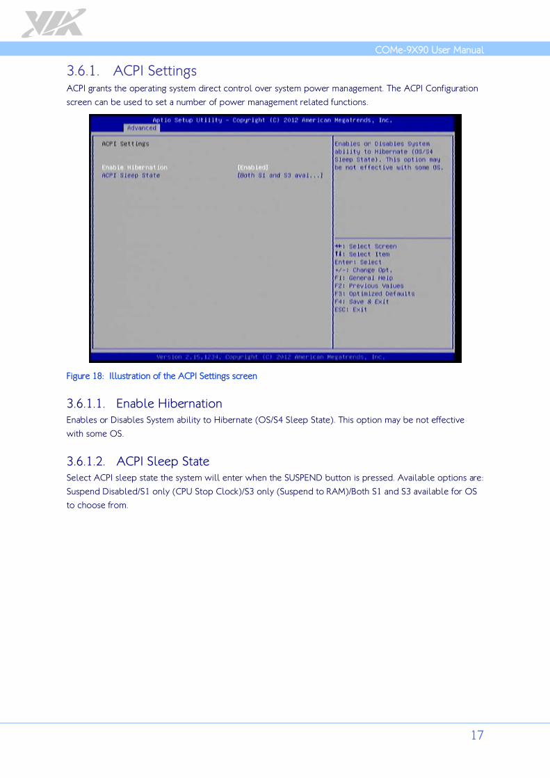
3.6.1. ACPI Settings ACPI grants the operating system direct control over system power management. The ACPI Configuration
screen can be used to set a number of power management related functions.
Figure 18: Illustration of the ACPI Settings screen
3.6.1.1. Enable Hibernation Enables or Disables System ability to Hibernate (OS/S4 Sleep State). This option may be not effective
with some OS.
3.6.1.2. ACPI Sleep State Select ACPI sleep state the system will enter when the SUSPEND button is pressed. Available options are:
Suspend Disabled/S1 only (CPU Stop Clock)/S3 only (Suspend to RAM)/Both S1 and S3 available for OS
to choose from.
COMe-9X90 User Manual
18
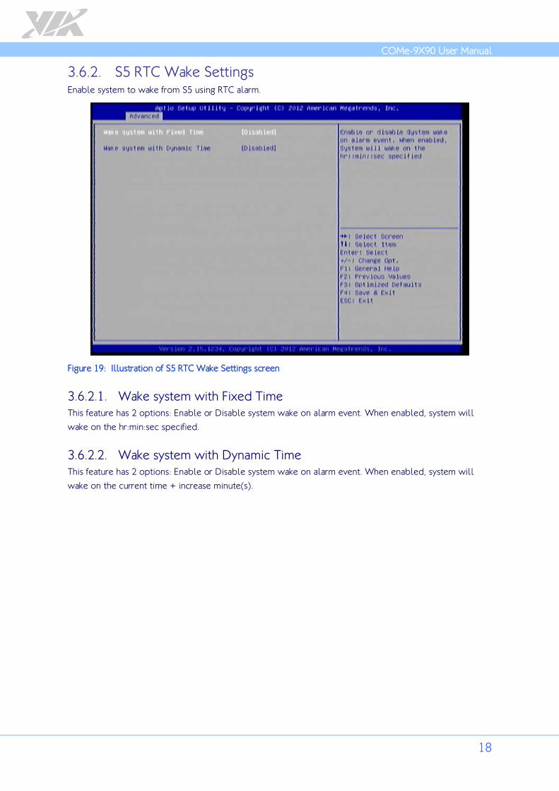
3.6.2. S5 RTC Wake Settings Enable system to wake from S5 using RTC alarm.
Figure 19: Illustration of S5 RTC Wake Settings screen
3.6.2.1. Wake system with Fixed Time This feature has 2 options: Enable or Disable system wake on alarm event. When enabled, system will
wake on the hr:min:sec specified.
3.6.2.2. Wake system with Dynamic Time This feature has 2 options: Enable or Disable system wake on alarm event. When enabled, system will
wake on the current time + increase minute(s).
COMe-9X90 User Manual
19
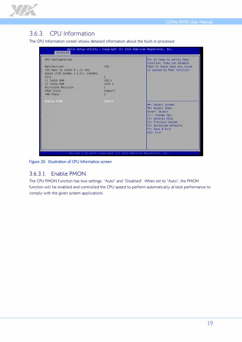
3.6.3. CPU Information The CPU Information screen shows detailed information about the built-in processor.
Figure 20: Illustration of CPU Information screen
3.6.3.1. Enable PMON The CPU PMON Function has two settings: “Auto” and “Disabled”. When set to “Auto”, the PMON
function will be enabled and controlled the CPU speed to perform automatically at best performance to
comply with the given system applications.
COMe-9X90 User Manual
20
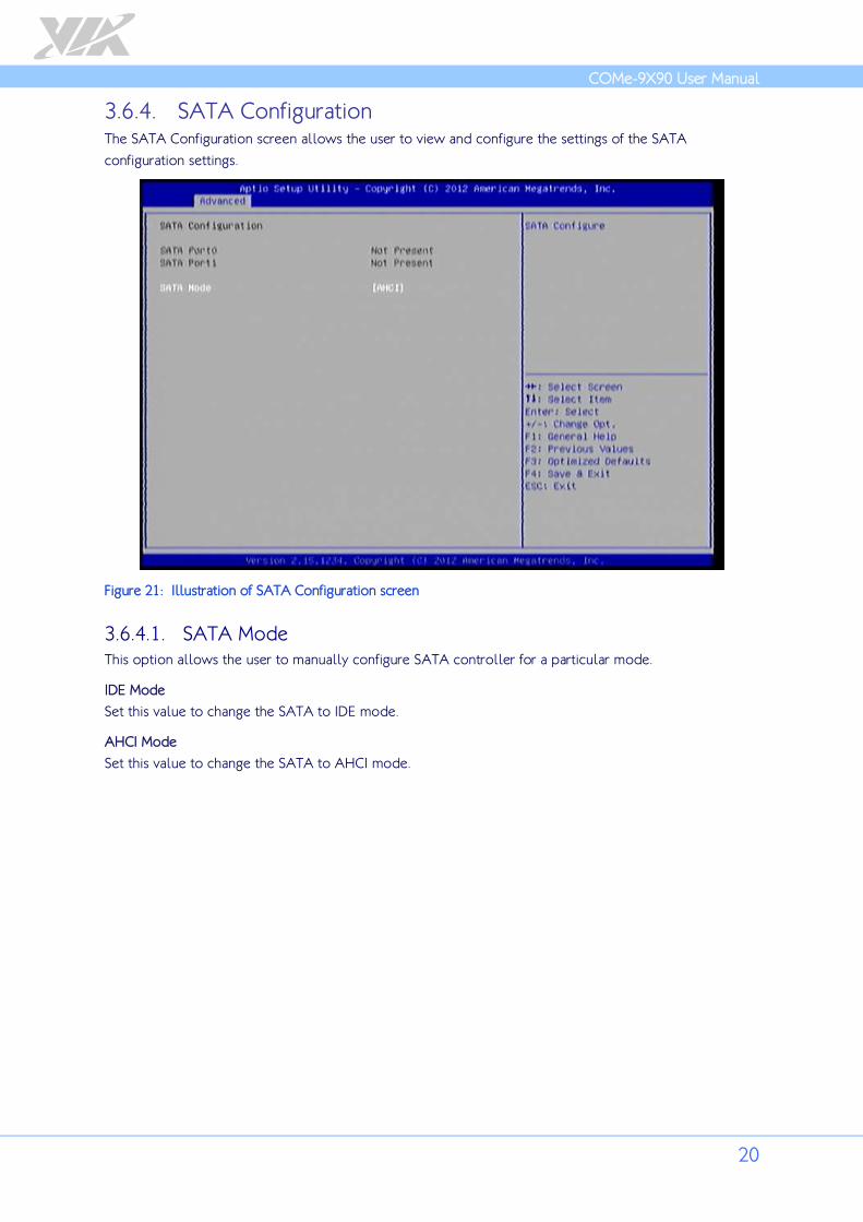
3.6.4. SATA Configuration The SATA Configuration screen allows the user to view and configure the settings of the SATA
configuration settings.
Figure 21: Illustration of SATA Configuration screen
3.6.4.1. SATA Mode This option allows the user to manually configure SATA controller for a particular mode.
IDE Mode
Set this value to change the SATA to IDE mode.
AHCI Mode
Set this value to change the SATA to AHCI mode.

COMe-9X90 User Manual
21
3.6.5. USB Configuration The USB Configuration screen allows the user to configure the USB configuration settings.
Figure 22: Illustration of USB Configuration screen
3.6.5.1. Legacy USB Support The Legacy USB Support feature enables environments that do not have native USB support to use USB
devices. This feature has three options.
Auto
The Auto option automatically disables legacy support if no USB devices are connected.
Enabled
The Enabled option keeps the Legacy USB Support feature on at all times.
Disabled
The Disabled option keeps the Legacy USB Support feature off at all times.
3.6.5.2. USB3.0 Support Enable/Disable USB3.0 (XHCI) Controller support.
3.6.5.3. XHCI Hand-off This is a workaround for Operating Systems without XHCI hand-off support. The XHCI ownership change
should be claimed by XHCI driver.

COMe-9X90 User Manual
22
3.6.5.4. EHCI Hand-off This is a workaround feature for Operating Systems without EHCI hand-off support. The EHCI ownership
must be claimed by EHCI Driver.
Enabled
This option enables EHCI hand-off support.
Disabled
This option disables EHCI hand-off support.
3.6.5.5. USB Mass Storage Driver Support Enable/Disable USB Mass Storage Driver Support.
USB hardware delays and time-outs:
3.6.5.6. USB transfer time-out The time-out value for Control, Bulk and Interrupt transfers. This feature has 4 options: 1 sec/5 sec/10
sec/20 sec.
3.6.5.7. Device reset time-out This feature enables user to set Device Rest Timeout at various time intervals. The options are: 10 sec/20
sec/30 sec/40 sec.
3.6.5.8. Device power-up delay Maximum time the device will take before it properly reports itself to the Host Controller. This feature
has 2 options: Auto/Manual. “Auto” uses default value: for a Root port it is 100 ms, for a Hub port the
delay is taken from Hub descriptor.
COMe-9X90 User Manual
23
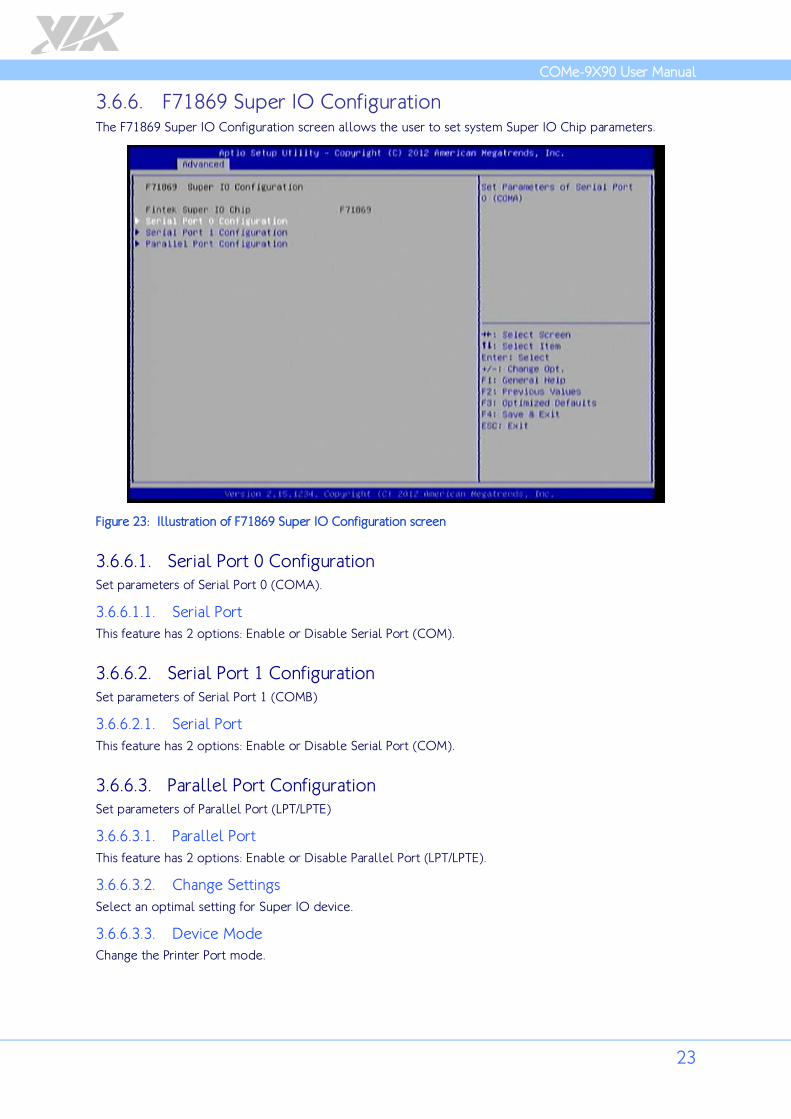
3.6.6. F71869 Super IO Configuration The F71869 Super IO Configuration screen allows the user to set system Super IO Chip parameters.
Figure 23: Illustration of F71869 Super IO Configuration screen
3.6.6.1. Serial Port 0 Configuration Set parameters of Serial Port 0 (COMA).
3.6.6.1.1. Serial Port This feature has 2 options: Enable or Disable Serial Port (COM).
3.6.6.2. Serial Port 1 Configuration Set parameters of Serial Port 1 (COMB)
3.6.6.2.1. Serial Port This feature has 2 options: Enable or Disable Serial Port (COM).
3.6.6.3. Parallel Port Configuration Set parameters of Parallel Port (LPT/LPTE)
3.6.6.3.1. Parallel Port This feature has 2 options: Enable or Disable Parallel Port (LPT/LPTE).
3.6.6.3.2. Change Settings Select an optimal setting for Super IO device.
3.6.6.3.3. Device Mode Change the Printer Port mode.

COMe-9X90 User Manual
24
3.6.7. F71869 H/W Monitor F71869 H/W Monitor shows Monitor hardware status.
Figure 24: Illustration of F71869 H/W Monitor screen
3.6.8. F75308 H/W Monitor F75308 H/W Monitor shows PC health status.
Figure 25: Illustration of F75308 H/W Monitor screen
COMe-9X90 User Manual
25
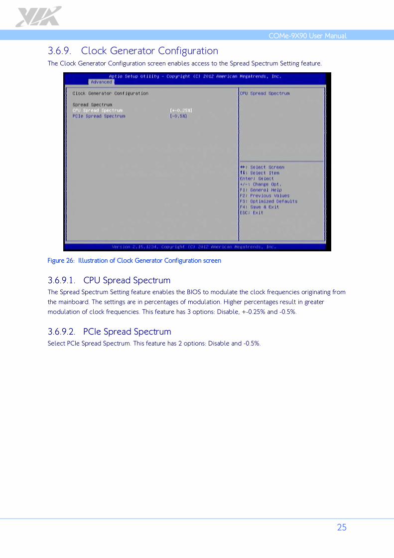
3.6.9. Clock Generator Configuration The Clock Generator Configuration screen enables access to the Spread Spectrum Setting feature.
Figure 26: Illustration of Clock Generator Configuration screen
3.6.9.1. CPU Spread Spectrum The Spread Spectrum Setting feature enables the BIOS to modulate the clock frequencies originating from
the mainboard. The settings are in percentages of modulation. Higher percentages result in greater
modulation of clock frequencies. This feature has 3 options: Disable, +-0.25% and -0.5%.
3.6.9.2. PCIe Spread Spectrum Select PCIe Spread Spectrum. This feature has 2 options: Disable and -0.5%.
COMe-9X90 User Manual
26
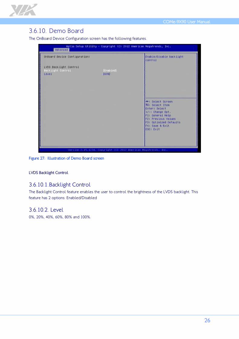
3.6.10. Demo Board The OnBoard Device Configuration screen has the following features.
Figure 27: Illustration of Demo Board screen
LVDS Backlight Control
3.6.10.1. Backlight Control The Backlight Control feature enables the user to control the brightness of the LVDS backlight. This
feature has 2 options: Enabled/Disabled
3.6.10.2. Level 0%, 20%, 40%, 60%, 80% and 100%.

COMe-9X90 User Manual
27
3.7. Chipset Settings The Chipset Settings screen shows a list of categories that can provide access to a sub-screen. Sub-screen
links can be identified by the preceding right-facing arrowhead.
Figure 28: Illustration of Chipset Settings screen
The Chipset Settings screen contains the following links:
• North Bridge
• South Bridge

COMe-9X90 User Manual
28
3.7.1. North Bridge The North Bridge screen contains the following links:
• DRAM Configuration
• Video Configuration
Figure 29: Illustration of North Bridge screen
COMe-9X90 User Manual
29
3.7.1.1. DRAM Configuration The DRAM Configuration screen has two features for controlling the system DRAM. All other DRAM
features are automated and cannot be accessed.
Figure 30: Illustration of DRAM Configuration screen
3.7.1.1.1. DRAM Clock The DRAM Clock option enables the user to determine how the BIOS handles the memory clock
frequency. The memory clock can either be dynamic or static. This feature has eleven options.
By SPD
By SPD option enables the BIOS to select a compatible clock frequency for the installed memory.
400 MHz
The 400 MHz option forces the BIOS to be fixed at 800 MHz for DDR3 memory modules.
533 MHz
The 533 MHz option forces the BIOS to be fixed at 1066 MHz for DDR3 memory modules.
566 MHz
The 566 MHz option forces the BIOS to be fixed at 1132 MHz for DDR3 memory modules.
600 MHz
The 600 MHz option forces the BIOS to be fixed at 1200 MHz for DDR3 memory modules.
633 MHz
The 633 MHz option forces the BIOS to be fixed at 1266 MHz for DDR3 memory modules.
667 MHz
The 667 MHz option forces the BIOS to be fixed at 1334 MHz for DDR3 memory modules.
700 MHz
The 700 MHz option forces the BIOS to be fixed at 1400 MHz for DDR3 memory modules

COMe-9X90 User Manual
30
733 MHz
The 733 MHz option forces the BIOS to be fixed at 1466 MHz for DDR3 memory modules
766 MHz
The 766 MHz option forces the BIOS to be fixed at 1532 MHz for DDR3 memory modules
800 MHz
The 800 MHz option forces the BIOS to be fixed at 1600 MHz for DDR3 memory modules
3.7.1.1.2. VGA Share Memory (Frame Buffer) The VGA Share Memory feature enables the user to choose the amount of the system memory to reserve
for use by the integrated graphics controller. The selections of memory amount that can be reserved are
256MB and 512MB.
3.7.1.2. Video Configuration The Video Configuration screen has features for controlling the integrated graphics controller in the VX11
chipset.
Figure 31: Illustration of Video Configuration screen
3.7.1.2.1. Select Display Device Control Available selections are: Auto and Manual.
3.7.1.2.2. Select Display Device 1 and 2 The Select Display Device feature enables the user to choose a specific display interface. This feature has
four options: CRT, LCD, DP2 and DP. If both Select Display Device 1 and Select Display Device 2 are set
to the same interface, then any display device connected to the other interface will not function. For
example, if both Select Display 1 and 2 are set to CRT, then no data will be sent to the LCD, DP2 and DP
port.
COMe-9X90 User Manual
31
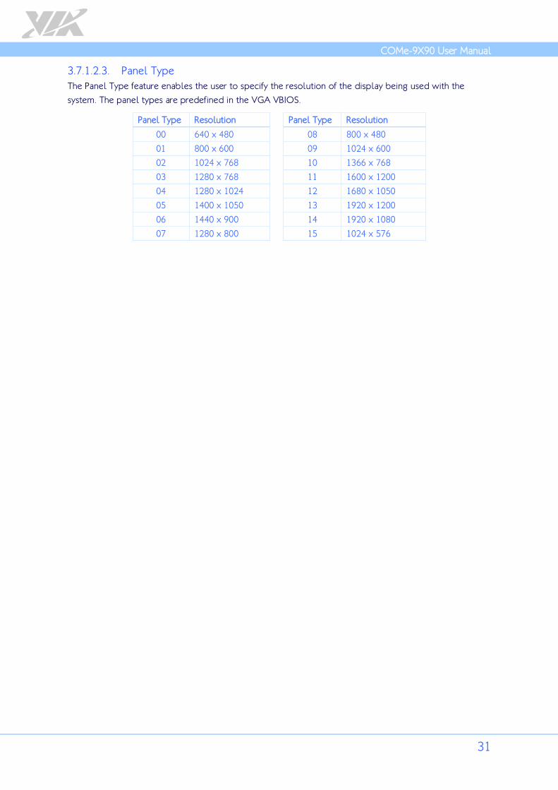
3.7.1.2.3. Panel Type The Panel Type feature enables the user to specify the resolution of the display being used with the
system. The panel types are predefined in the VGA VBIOS.
Panel Type Resolution
Panel Type Resolution
00 640 x 480 08 800 x 480
01 800 x 600 09 1024 x 600
02 1024 x 768 10 1366 x 768
03 1280 x 768 11 1600 x 1200
04 1280 x 1024 12 1680 x 1050
05 1400 x 1050 13 1920 x 1200
06 1440 x 900 14 1920 x 1080
07 1280 x 800 15 1024 x 576
COMe-9X90 User Manual
32
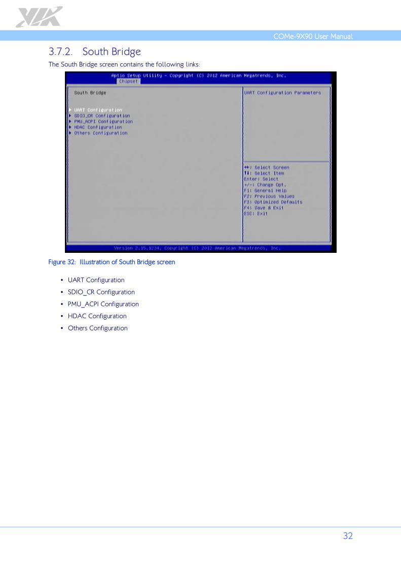
3.7.2. South Bridge The South Bridge screen contains the following links:
Figure 32: Illustration of South Bridge screen
• UART Configuration
• SDIO_CR Configuration
• PMU_ACPI Configuration
• HDAC Configuration
• Others Configuration
COMe-9X90 User Manual
33
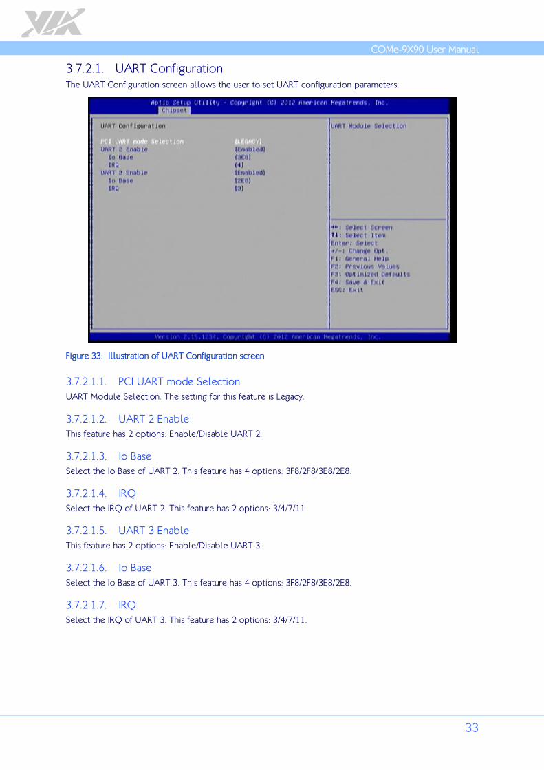
3.7.2.1. UART Configuration The UART Configuration screen allows the user to set UART configuration parameters.
Figure 33: Illustration of UART Configuration screen
3.7.2.1.1. PCI UART mode Selection UART Module Selection. The setting for this feature is Legacy.
3.7.2.1.2. UART 2 Enable This feature has 2 options: Enable/Disable UART 2.
3.7.2.1.3. Io Base Select the Io Base of UART 2. This feature has 4 options: 3F8/2F8/3E8/2E8.
3.7.2.1.4. IRQ Select the IRQ of UART 2. This feature has 2 options: 3/4/7/11.
3.7.2.1.5. UART 3 Enable This feature has 2 options: Enable/Disable UART 3.
3.7.2.1.6. Io Base Select the Io Base of UART 3. This feature has 4 options: 3F8/2F8/3E8/2E8.
3.7.2.1.7. IRQ Select the IRQ of UART 3. This feature has 2 options: 3/4/7/11.
COMe-9X90 User Manual
34
3.7.2.2. SDIO_CR Configuration The SDIO_CR Configuration screen allows the user to set SDIO_CR configuration parameters.
Figure 34: Illustration of SDIO_CR Configuration screen
3.7.2.2.1. SDIO Host controller This feature has 2 options: Enable or Disable SDIO Host controller.
3.7.2.2.2. Voltage Support 1.6v This feature has 2 options: Enable or Disable Voltage Support 1.6v.
3.7.2.2.3. High Speed Support This feature has 2 options: Enable or Disable High Speed Support.
3.7.2.2.4. Base Clock Frequency For SD Clock This feature has 2 options: By FSB/200MHZ
By selecting “By FSB”, the base clock frequency will be changed to FSB/B.
3.7.2.2.5. Driver Type Select Select Driver Type from Type A/ Type B/ Type C/ Type D.
3.7.2.2.6. SDR50 Support This feature has 2 options: Enable or Disable SDR50 Support.
3.7.2.2.7. SDR104 Support This feature has 2 options: Enable or Disable SDR104 Support.
3.7.2.2.8. DDR50 Support This feature has 2 options: Enable or Disable DDR50 Support.
COMe-9X90 User Manual
35
3.7.2.2.9. SDR50 Tuning Enable This feature has 2 options: Enable or Disable SDR50 Tuning Enable.
3.7.2.2.10. Timer Count for Re-Tuning Set SDIO Timer count for re-tuning. Available options are: Re-tuning Timer Disabled/1 sec/2 secs/4 secs/8
secs/16 secs/32 secs/64 secs/128 secs/256 secs/512 secs/1024 secs/Get information from other source

COMe-9X90 User Manual
36
3.7.2.3. PMU_ACPI Configuration The PMU_ACPI Configuration screen can be used to set a number of power management related functions.
Figure 35: Illustration of PMU_ACPI Configuration screen
3.7.2.3.1. Other Control
Figure 36: Illustration of Other Control screen
COMe-9X90 User Manual
37
3.7.2.3.1.1. AC Loss Auto-restart
AC Loss Auto-restart defines how the system will respond after AC power has been interrupted while the
system is on. There are three options.
Power Off
The Power Off option keeps the system in an off state until the power button is pressed again.
Power On
The Power On option restarts the system when the power has returned.
Last State
The Last State option restores the system to its previous state when the power was interrupted.
3.7.2.3.1.2. USB S4 WakeUp
The USB S4 WakeUp enables the system to resume through the USB device port from S4 state. There are
two options: “Enabled” or “Disabled”.
3.7.2.4. HDAC Configuration HDAC Configuration Parameters.
Figure 37: Illustration of HDAC Configuration screen
3.7.2.4.1. OnChip HDAC Device This feature has 2 options: Enable or Disable HDAC Control.

COMe-9X90 User Manual
38
3.7.2.5. Others Configuration The Others Configuration screen can be used to set Watchdog Timer Configuration and Keyboard/Mouse
Wakeup Configuration.
Figure 38: Illustration of Others Configuration screen
3.7.2.5.1. WATCHDOG Timer Enable When this feature is enabled, an embedded timing device automatically prompts corrective action upon
system malfunction detection.

COMe-9X90 User Manual
39
3.8. Boot Settings The Boot Settings screen has a single link that goes to the Boot Configuration and Boot Option Priorities
screens.
Figure 39: Illustration of Boot Settings screen
3.8.1. Boot Configuration The Boot Settings Configuration screen has several features that can be run during the system boot
sequence.
3.8.1.1. Setup Prompt Timeout Number of seconds to wait for setup activation key. 65535(0xFFFF) means indefinite waiting.
3.8.1.2. BootupNumLock State Select the keyboard NumLock state from On and Off.
3.8.1.3. Display Logo The Display Logo feature hides all of the Power-on Self Test (POST) messages during the boot sequence.
Instead of the POST messages, the user will see an OEM logo. This feature has two options: enabled and
disabled.
3.8.1.4. Fast Boot Enables or Disables boot with initialization of a minimal set of devices required to launch active boot
option. It has no effect for BBS boot options.
COMe-9X90 User Manual
40
3.8.2. Boot Option Priorities The Boot Option Priorities screen lists all bootable devices.
3.8.2.1. Boot Option #1 Sets the system boot order. This feature has two options: Realtek PXE 801 D00 /Disabled.
3.8.3. Network Device BBS Priorities Set the order of the legacy devices in this group.
3.8.3.1. Boot Option #1 Set the system boot order. This feature has two options: Realtek PXE 801 D00 /Disabled.
3.8.4. CSM parameters OpROM execution, boot options filter, etc.
3.8.4.1. Launch CSM This option controls if CSM will be launched. This feature has two options: Enabled/Disabled.
3.8.4.2. Boot option filter This option controls what devices system can boot to. This feature has 3 options: UEFI and Legacy/Legacy
only/UEFI only.
3.8.4.3. Launch PXE OpROM policy Controls the execution of UEFI and Legacy PXE OpROM. This feature has 2 options: Do not launch/Legacy
only.
3.8.4.4. Launch Storage OpROM policy Controls the execution of UEFI and Legacy Storage OpROM. This feature has 3 options: Do not
launch/UEFI only/Legacy only.
3.8.4.5. Launch Video OpROM policy Controls the execution of UEFI and Legacy Video OpROM. This feature has 3 options: Do not launch/UEFI
only/Legacy only.
3.8.4.6. Other PCI device ROM priority For PCI devices other than Network, Mass storage or video defines which OpROM to launch. This feature
has 2 options: UEFI OpROM/Legacy OpROM.

COMe-9X90 User Manual
41
3.9. Security Settings The Security Settings screen provides a way to restrict access to the BIOS or even the entire system.
Figure 40: Illustration of Security Settings screen
3.9.1. Security Settings
3.9.1.1. Administrator Password / User Password This option is for setting a password for accessing the BIOS setup utility. When a password has been set, a
password prompt will be displayed whenever the BIOS setup utility is launched. This prevents an
unauthorized person from changing any part of the system configuration.
When a supervisor password is set, the Password Check option will be unlocked.
3.9.1.2. Password Check This feature is compulsory when the Change Supervisor Password option is set. The user will have up to
three chances to enter the correct password before the BIOS forces the system to stop booting. If the user
does not enter the correct password, the keyboard will also lock up. The only way to get past this is to
do a hard reboot (i.e., use the system reset button or cut off the power to the system). A soft reboot (i.e.,
Ctrl+Alt+Del) will not work because the keyboard will be locked. This feature has two options.
Setup
The Setup option forces users to enter a password in order to access the BIOS Setup Utility.
Always
The Always option forces users to enter a password in order to boot up the system.

COMe-9X90 User Manual
42
3.10. Save & Exit Options The Save & Exit Configuration screen has the following features:
Figure 41: Illustration of Save & Exit Options screen
3.10.1. Save Changes and Exit Save all changes to the BIOS and exit the BIOS Setup Utility. The “F4” hotkey can also be used to trigger
this command.
3.10.2. Discard Changes and Exit Exit the BIOS Setup Utility without saving any changes. The “Esc” hotkey can also be used to trigger this
command.
3.10.3. Save Changes and Reset Save all changes to the BIOS and reboot the system. The new system configuration parameters will take
effect.
3.10.4. Discard Changes and Reset This command reverts all changes to the settings that were in place when the BIOS Setup Utility was
launched.

COMe-9X90 User Manual
43
Save Options
3.10.5. Save Changes Save Changes done so far to any of the setup options.
3.10.6. Discard Changes This command reverts all changes to the settings that were in place when the BIOS Setup Utility was
launched.
Restore Default
3.10.7. Save as User Defaults Save the changes done so far as User Defaults.
3.10.8. Restore User Defaults Restore the User Defaults to all the setup options.
Boot Override
3.10.9. Realtek PXE B01 D00
COMe-9X90 User Manual
44
4. Driver Installation
4.1. Microsoft Driver Support The VIA COMe-9X90 mainboard is compatible with Microsoft operating systems. The latest Windows
drivers can be downloaded from the VIA website at www.viatech.com.
For embedded operating systems, the related drivers can be found in the VIA website at
www.viatech.com.
4.2. Linux Driver Support The VIA COMe-9X90 mainboard is highly compatible with many Linux distributions.
Support and drivers are provided through various methods including:
� Drivers provided by VIA
� Using a driver built into a distribution package
� Visiting www.viatech.com for the latest updated drivers
� Installing a third party driver (such as the ALSA driver from the Advanced Linux Sound Architecture
project for integrated audio)
For OEM clients and system integrators developing a product for long term production, other code and
resources may also be made available. Contact VIA to submit a request.
COMe-9X90 User Manual
45
Appendix A. COMEDB4 Carrier Board
A.1. Board Specifications
COM Express™ Module Type
Support basic/compact form factor Type 6
Audio
VIA VT2021 High Definition Audio Codec
Super I/O
Fintek F71869ED
BIOS
AMI BIOS
32Mbit SPI BIOS for uEFI
Front Panel I/O
1 x SD card slot (SDIO) as default, shared with DIO1 pin header
Rear Panel I/O
1 x VGA port
1 x COM port
2 x DisplayPort
2 x USB 2.0 ports
2 x USB 3.0 ports
1 x Gigabit Ethernet port
6 x Audio jacks (supports multi-channel audio outputs)
Onboard Slots, Buttons and Power Connectors
1 x AUX power connector (for AT mode)
1 x ATX power connector (for ATX mode)
1 x MiniPCIe slot
1 x Power button
1 x Reset button
3 x PCIe x1 slots
2 x SATA connectors
Onboard Pin Headers and Connectors
1 x CD-In connector
1 x Front Audio pin header
1 x COM2 pin header
1 x LPT pin header
1 x LPC pin header
1 x SPI pin header

COMe-9X90 User Manual
46
1 x DIO1 pin header, shared with SDIO slot
1 x DIO2 pin header (from Fintek F71869ED)
1 x CPU fan connector
1 x Serial Port pin header
2 x SATA power connectors
1 x LVDS panel connector (dual-channel 18/24-bit)
1 x Inverter connector
1 x System fan connector
1 x SMBus pin header
1 x I2C pin header
2 x USB 2.0 pin headers for four USB 2.0 ports
1 x Front LAN LED pin header
1 x Front Panel pin header (for HDD LED, Power LED, Switch and Speaker)
1 x S/PDIF connector
Onboard Jumpers
1 x Clear CMOS jumper
1 x Inverter power select jumper
1 x LCD panel power select jumper
1 x COM1 voltage select jumper (+5V/+12V power select option)
1 x COM2 voltage select jumper (+5V/+12V power select option)
1 x MiniPCIe slot enabled select jumper
1 x USB 2.0 port 3 enabled select jumper
1 x BIOS select jumper (for selecting module/carrier board BIOS)
5 x AT/ATX mode select jumpers
1 x EDID power select jumper
Form Factor and Dimension
Micro-ATX
10” x 9.6”
Operating Temperature
0°C ~ 60°C
Storage Temperature
-40°C ~ 70°C
Operating Humidity
0% ~ 95% relative humidity
COMe-9X90 User Manual
47
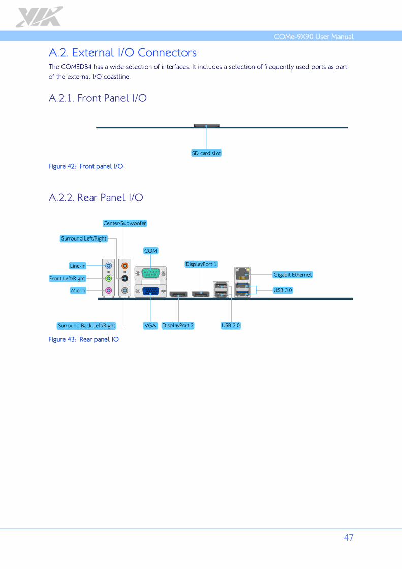
A.2. External I/O Connectors The COMEDB4 has a wide selection of interfaces. It includes a selection of frequently used ports as part
of the external I/O coastline.
A.2.1. Front Panel I/O
SD card slot
Figure 42: Front panel I/O
A.2.2. Rear Panel I/O
VGA DisplayPort 2
COM
Gigabit Ethernet
Line-in
Mic-in
Surround Left/Right
Surround Back Left/Right
Center/Subwoofer
DisplayPort 1
USB 2.0
USB 3.0
Front Left/Right
Figure 43: Rear panel IO

COMe-9X90 User Manual
48
A.3. COMEDB4 Layout Diagram
A.3.1. Onboard Slots, Buttons and Power Connectors
COMEDB4COMEDB4
PCIe x1 slots
Connector A
Connector B
SATA connectors
Power button
Reset button
miniPCIe slot
AUX power connector
ATX power connector
Figure 44: COMEDB4 slots, buttons, and power connectors layout
COMe-9X90 User Manual
49
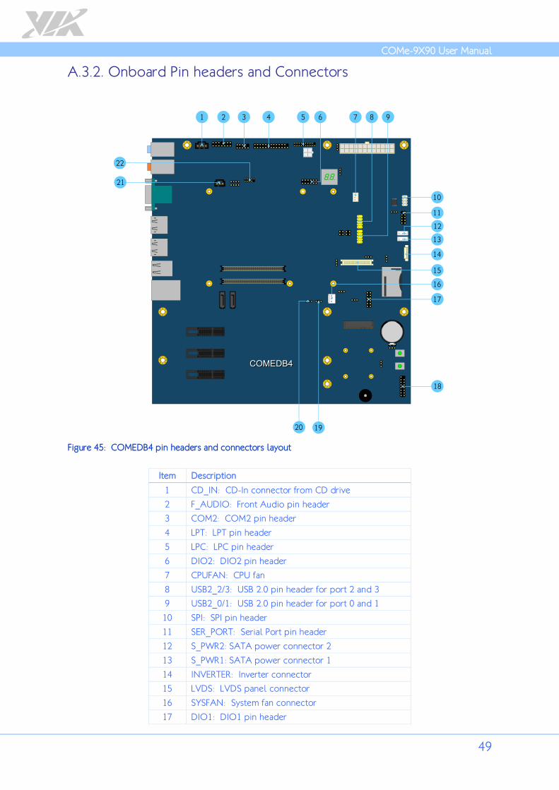
A.3.2. Onboard Pin headers and Connectors
Figure 45: COMEDB4 pin headers and connectors layout
Item Description
1 CD_IN: CD-In connector from CD drive
2 F_AUDIO: Front Audio pin header
3 COM2: COM2 pin header
4 LPT: LPT pin header
5 LPC: LPC pin header
6 DIO2: DIO2 pin header
7 CPUFAN: CPU fan
8 USB2_2/3: USB 2.0 pin header for port 2 and 3
9 USB2_0/1: USB 2.0 pin header for port 0 and 1
10 SPI: SPI pin header
11 SER_PORT: Serial Port pin header
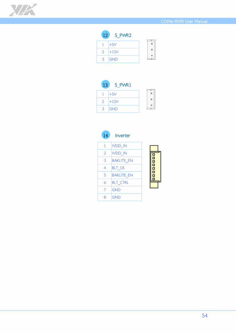
12 S_PWR2: SATA power connector 2
13 S_PWR1: SATA power connector 1
14 INVERTER: Inverter connector
15 LVDS: LVDS panel connector
16 SYSFAN: System fan connector
17 DIO1: DIO1 pin header
COMe-9X90 User Manual
50
18 F_PANEL: Front Panel pin header
19 I2C_BUS: I2C pin header
20 SMBUS: System Management Bus pin header
21 SPDIF: S/PDIF connector
22 FLAN_LED: Front LAN LED pin header
Table 2: Layout diagram description table of the COMEDB4 (pin headers and connectors)

COMe-9X90 User Manual
51
A.3.2.1. Pin Headers and Connectors Pin Definition
1 CD_IN_L
2 CD_IN_GND
3 CD_IN_GND
4 CD_IN_R
MIC2_FR_L 1
2 AGND
MIC2_FR_R 3 4 FNT_DET
HP_OUT_R 5 6 MIC2_JD
FNT_IO_SENSE 7 8 KEY
HP_OUT_L 9 10 LINE2_JD
+12V 11 12 +12V
AGND 13 14 AGND
COM_DCD2 1
2 COM_RXD2
COM_TXD2 3 4 COM_DTR2
GND 5 6 COM_DSR2
COM_RTS2 7 8 COM_CTS2
COM_RI2 9 10 KEY
CD_IN 1
F_AUDIO 2
COM2 3

COMe-9X90 User Manual
52
-LP_STB 1
2 -LP_AFD
LP_D0 3 4 -LP_ERR
LP_D1 5 6 -LP_INIT
LP_D2 7 8 -LP_SLIN
LP_D3 9 10 GND
LP_D4 11 12 GND
LP_D5 13 14 GND
LP_D6 15 16 GND
LP_D7 17 18 GND
-LP_ACK 19 20 GND
LP_BUSY 21 22 GND
LP_PE 23 24 GND
LP_SLCT 25 26 KEY
LPC_AD1 1
2 LPC_33M_CLK
-LPC_RESET 3 4 GND
LPC_AD0 5 6 NC
LPC_AD2 7 8 -LPC_FRAME
LPC_SERIRQ 9 10 LPC_AD3
-LPC_DRQ1 11 12 NC
+5V 13 14 +3.3V
+5V 15 16 +3.3V
GND 17 18 GND
GND 19 20 KEY
5V_DIO2 1
2 12V_DIO2
GPO34 3 4 GPI50
GPO35 5 6 GPI51
GPO36 7 8 GPI52
GPO37 9 10 GPI53
GND 11 12 GND
LPT 4
LPC 5
DIO2 6

COMe-9X90 User Manual
53
1 FANIO
2 FANPWM
3 GND
VUSB 1 2 VUSB
USBD_T2- 3 4 USBD_T3-
USBD_T2+ 5 6 USBD_T3+
GND 7 8 GND
KEY 9 10 GND
VUSB 1 2 VUSB
USBD_T0- 3 4 USBD_T1-
USBD_T0+ 5 6 USBD_T1+
GND 7 8 GND
KEY 9 10 GND
SPI_VCC 1 2 GND
-SPI_SS0 3 4 SPI_CLK
SPI_DI 5 6 SPI_DO
KEY 7 8 RESET
SER0_TX_CON 1 2 SER0_RX_CON
NC 3 4 NC
GND 5 6 NC
SER1_TX_CON 7 8 SER1_RX_CON
NC 9 10 KEY
CPUFAN 7
USB2_2/3 8
USB2_0/1 9
SPI 10
SER_PORT 11
COMe-9X90 User Manual
54
1 +5V
2 +12V
3 GND
1 +5V
2 +12V
3 GND
1 IVDD_IN
2 IVDD_IN
3 BAKLITE_EN
4 BLT_CK
5 BAKLITE_EN
6 BLT_CTRL
7 GND
8 GND
S_PWR2 12
S_PWR1 13
Inverter 14

COMe-9X90 User Manual
55
-A4_L 1 2 PVDD
A4_L 3 4 PVDD
GND 5 6 GND
-A5_L 7 8 GND
A5_L 9 10 -A0_L
GND 11 12 A0_L
-A6_L 13 14 GND
A6_L 15 16 -A1_L
GND 17 18 A1_L
-CLK2_L 19 20 GND
CLK2_L 21 22 -A2_L
GND 23 24 A2_L
-A7_L 25 26 GND
A7_L 27 28 -CLK1_L
NC 29 30 CLK1_L
NC 31 32 GND
DDC_PWR 33 34 -A3_L
NC 35 36 A3_L
NC 37 38 SPCLK
NC 39 40 SPD
1 FANIO
2 FANPWM
3 GND
5V_DIO1 1 2 12V_DIO1
COM_GPO0 3 4 COM_GPI0
COM_GPO1 5 6 COM_GPI1
COM_GPO2 7 8 COM_GPI2
COM_GPO3 9 10 COM_GPI3
GND 11 12 GND
LVDS 15
SYSFAN 16
DIO1 17

COMe-9X90 User Manual
56
FP_5V 1 2 FP_5V
FP_5V 3 4 -SATA_LED
-PLED 5 6 -PW_BTN
FP_5V 7 8 GND
NC 9 10 RST_SW
NC 11 12 GND
SPEAK 13 14 FP_5V
KEY 15 16 NC
1 I2C_CLK
2 I2C_DATA
3 GND
1 SMB_CLK
2 SMB_DATA
3 GND
1 +5V
2 SPDIFO
3 GND
3VSUS 1 2 -LAN_ACT
3VSUS 3 4 NC
GND 5 6 W_LAN_LED
3VSUS 7 8 GND
KEY 9 10 GND
F_PANEL 18
I2C BUS 19
SMBUS 20
SPDIF 21
FLAN_LED 22

COMe-9X90 User Manual
57
A.3.3. Onboard Jumpers
Figure 46: COMEDB4 jumpers layout
Item Description
23 JP_COM1_VSEL: COM1 voltage select jumper
24 JP_COM2_VSEL: COM2 voltage select jumper
25 JP_AT/ATX_SEL5: AT/ATX mode select jumper
26 JP_AT/ATX_SEL2: AT/ATX mode select jumper
27 JP_AT/ATX_SEL3: AT/ATX mode select jumper
28 JP_USBP3_SEL: USB 2.0 port 3 enabled select jumper
29 JP_USBME_SEL: MiniPCIe slot enabled select jumper
30 IVDD: Inverter power select jumper
31 EDID_PWR: EDID power select jumper
32 JP_AT/ATX_SEL4: AT/ATX mode select jumper
33 BIOS_DIS1: BIOS select jumper (for selecting module/carrier board BIOS)
34 PVDD: LCD panel power select jumper
35 JP_AT/ATX_SEL1: AT/ATX mode select jumper
36 CLEAR_CMOS: Clear CMOS jumper
Table 3: Layout diagram description table of the COMEDB4 (jumpers)

COMe-9X90 User Manual
58
A.3.3.1. Jumper Settings
Pins Description
1-2 Enabled COM1 pin header to support +5V
2-3 Normal (default)
3-4 Enabled COM1 pin header to support +12V
Pins Description
1-2 Enabled COM2 pin header to support +5V
2-3 Normal (default)
3-4 Enabled COM2 pin header to support +12V
Pins Description
1-2 ATX mode (default)
2-3 AT mode
Pins Description
1-2 ATX mode (default)
2-3 AT mode
JP_COM1_VSEL 23
JP_COM2_VSEL 24
JP_AT/ATX_SEL5 25
JP_AT/ATX_SEL2 26

COMe-9X90 User Manual
59
Pins Description
1-2 ATX mode (default)
2-3 AT mode
Pins Description
1-2 Enabled USB 2.0 port 3 pin header (default)
3-4 Enabled USB 2.0 port 3 pin header (default)
Pins Description
1-2 Enabled Mini PCIe slot
3-4 Enabled Mini PCIe slot
Pins Description
1-2 Use +5V for the Inverter power.
2-3 Use +12V for the Inverter power (default)
Pins Description
1-2 +3.3V (default)
3-4 +5V
Pins Description
1-2 ATX mode (default)
2-3 AT mode
Note: For [29] JP_USBME_SEL to be activated, the [28] JP_USBP3_SEL pin header function has to be disabled.
JP_AT/ATX_SEL3 27
JP_USBP3_SEL 28
JP_USBME_SEL 29
IVDD 30
EDID_PWR 31
JP_AT/ATX_SEL4 32
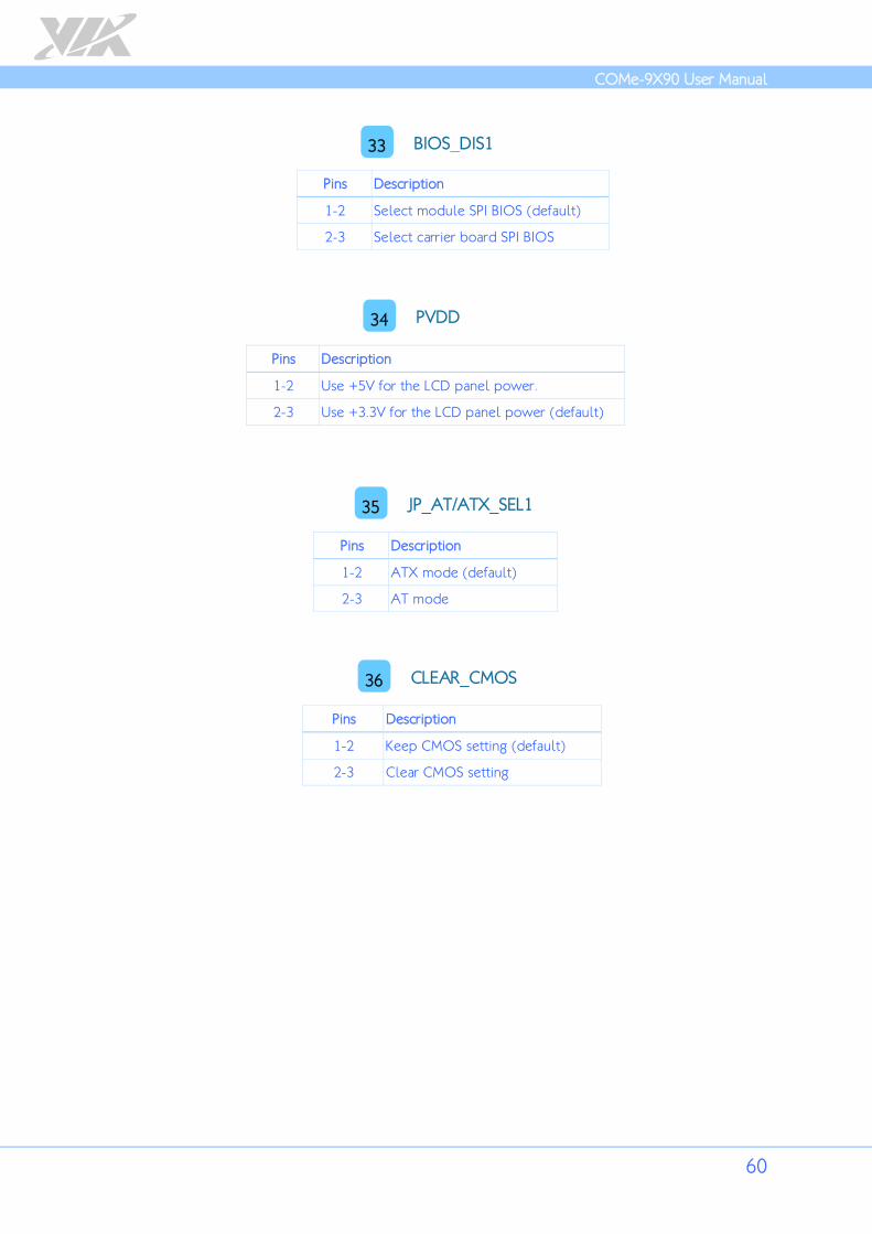
COMe-9X90 User Manual
60
Pins Description
1-2 Select module SPI BIOS (default)
2-3 Select carrier board SPI BIOS
Pins Description
1-2 Use +5V for the LCD panel power.
2-3 Use +3.3V for the LCD panel power (default)
Pins Description
1-2 ATX mode (default)
2-3 AT mode
Pins Description
1-2 Keep CMOS setting (default)
2-3 Clear CMOS setting
BIOS_DIS1 33
PVDD 34
JP_AT/ATX_SEL1 35
CLEAR_CMOS 36


