
Universita degli Studi di Pavia
Dipartimento di Elettronica
Corso di Dottorato in Ingegneria Elettronica,
Informatica ed Elettrica - XXIV ciclo
Tunable and narrow linewidthmm-wave generation through
monolithically integratedphase-locked DFB lasers
Design, Fabrication and Characterization
Advisor:
Prof. Guido Giuliani
Co-Advisor:
Dr. Michael J. Strain
PhD Thesis by
Marco Zanola
Anno accademico 2011

.
...alla mia mamma

Contents
Introduction 6
1 Photonic techniques for high-frequency signal generation 11
1.1 Applications of mm- and THz- waves . . . . . . . . . . . . . . 12
1.2 Generation of mm- and THz- waves . . . . . . . . . . . . . . . 14
1.3 Photonic techniques for mm- and THz- wave generation . . . . 16
1.4 Photomixing assisted by mutual injection locking and Four
Wave Mixing . . . . . . . . . . . . . . . . . . . . . . . . . . . 19
1.5 Integration into a single optoelectronic device . . . . . . . . . 25
2 Device Design 27
2.1 Device geometries . . . . . . . . . . . . . . . . . . . . . . . . . 28
2.2 Material description . . . . . . . . . . . . . . . . . . . . . . . . 31
2.3 Waveguides . . . . . . . . . . . . . . . . . . . . . . . . . . . . 33
2.4 DFB design . . . . . . . . . . . . . . . . . . . . . . . . . . . . 37
2.4.1 Coupled-wave equations . . . . . . . . . . . . . . . . . 38
2.4.2 Grating design . . . . . . . . . . . . . . . . . . . . . . 41
2.4.3 DFB for single mode operation . . . . . . . . . . . . . 46
2.4.4 Side-etched gratings for post-growth fabrication . . . . 52
2.5 Couplers . . . . . . . . . . . . . . . . . . . . . . . . . . . . . . 56
2.5.1 Evanescent field coupler . . . . . . . . . . . . . . . . . 57
2.5.2 MMI . . . . . . . . . . . . . . . . . . . . . . . . . . . . 60
2.6 Design summary . . . . . . . . . . . . . . . . . . . . . . . . . 66
CONTENTS 4
3 Fabrication 67
3.1 Mask realisation . . . . . . . . . . . . . . . . . . . . . . . . . . 68
3.2 Electron Beam Lithography . . . . . . . . . . . . . . . . . . . 68
3.3 Process overview . . . . . . . . . . . . . . . . . . . . . . . . . 70
3.4 Sample preparation . . . . . . . . . . . . . . . . . . . . . . . . 71
3.4.1 Markers definition and lift-off technique . . . . . . . . . 72
3.5 Waveguides definition . . . . . . . . . . . . . . . . . . . . . . . 74
3.5.1 Reactive Ion Etching . . . . . . . . . . . . . . . . . . . 77
3.5.2 Effect of RIE-lag . . . . . . . . . . . . . . . . . . . . . 79
3.6 Waveguide isolation and quasi-planarization . . . . . . . . . . 83
3.7 Contact windows opening . . . . . . . . . . . . . . . . . . . . 85
3.8 Metal depositions . . . . . . . . . . . . . . . . . . . . . . . . . 86
3.9 Cleaving and mounting . . . . . . . . . . . . . . . . . . . . . . 90
4 DFB characterization 92
4.1 L-I curves and wavelength maps . . . . . . . . . . . . . . . . . 92
4.2 Linewidth . . . . . . . . . . . . . . . . . . . . . . . . . . . . . 95
4.3 Coupling coefficient and stop-band measurements . . . . . . . 98
4.4 Ith and SMSR vs. different κL product values . . . . . . . . . 102
4.5 Measurements of Bragg wavelength spacing . . . . . . . . . . . 105
4.5.1 Wavelength spacing below threshold . . . . . . . . . . 107
4.5.2 Wavelength spacing above threshold . . . . . . . . . . 108
4.6 Stability measurements . . . . . . . . . . . . . . . . . . . . . . 111
5 Mutual Injection-Locking experiments 114
5.1 Mutual injection-locking of two DFBs . . . . . . . . . . . . . . 115
5.1.1 DFB linewidth narrowing under locked condition . . . 122
5.2 FWM efficiency . . . . . . . . . . . . . . . . . . . . . . . . . . 123
5.3 Mutual injection-locking of three DFBs assisted by FWM . . . 127
5.3.1 Methodology and demonstration of the phase locking . 129
5.3.2 Tunability of the RF signal . . . . . . . . . . . . . . . 138
5.3.3 Locking range vs. injected power . . . . . . . . . . . . 140

CONTENTS 5
5.3.4 RF signal linewidth vs. RF signal frequency . . . . . . 143
5.3.5 RF signal linewidth vs. injected power . . . . . . . . . 144
5.3.6 High-frequency measurements . . . . . . . . . . . . . . 148
Conclusions 152
Bibliography 159
Acknowledgements 173

Introduction
During the last couple of decades, the generation of high electrical fre-
quency signals (with frequencies from a few GHz up to the THz domain) has
been the subject of exhaustive research studies. Despite the wide range of
potential applications, the THz range is currently poorly developed due to
difficulties encountered in the generation of these signals. In fact, this range
of frequencies lies right in between the well-developed microwave and optical
domains.
Applications such as high-speed telecommunications, radio astronomy, spec-
troscopy, tomography and homeland security could be remarkably improved
by the availability of sources capable to emit efficiently in this range. The
range 40-60 GHz represents the next unlicensed frequency band, which can
used to offer a wide number of new services for indoor wireless communi-
cations. Local oscillators for radio astronomy and spectroscopy applications
are also required, with emission frequencies of a few hundred GHz and stable
and narrow linewidth. THz- waves can be successfully employed in novel
tomography spectroscopy and screening applications, thanks to their non-
ionising energies intrinsically safe for human beings. Finally, these waves
offer a high-contrast penetration of non-conductive (such as clothes) and
conductive (metals) materials, which can be used for homeland security ap-
plications (like mm- and THz- wave scanners).
Both electronics and optoelectronic approaches have been explored aiming
the generation of mm- and THz- waves, obtaining encouraging results. How-
ever, so far none of the available techniques has proven to be able to generate

CONTENTS 7
signals in the above-mentioned frequency range, by means of a single, effi-
cient, compact and reliable device. Such a device is required to generate
signals with high spectral purity (narrow linewidth and low phase noise)
that can be continuously tuned over the whole range of frequencies; the de-
mand for field-deployment requires stable room-temperature operation and
the control of a limited number of its parameters.
A promising optoelectronic technique has been recently proposed [1], which
represents an improvement of the basic Photomixing technique. It is based
on the mutual injection of three single mode lasers, which are all-optically
phase-locked via a Four Wave Mixing non-linear process. The beating of the
three lasers on a high speed photodetector is expected to generate a spec-
trally pure RF signal. Wide tunability of the generated RF signal can be
achieved by tuning the driving currents of the lasers, thus changing their
relative frequency separation.
Aim of the present work
The photomixing technique assisted by mutual injection locking and Four
Wave Mixing gave promising results using an experimental setup composed
of discrete optical components [1]. Three Distributed FeedBack (DFB) lasers
have been mutually injected using single mode optical fibres and couplers,
and an effective phase-locking between the lasers has been achieved.
The present work, funded by Fondazione Cariplo (Project 2007-
5263, ”Semiconductor lasers with nanostructured gratings for wire-
less application signal generation”), aims at the integration of that
complex discrete setup into a single monolithic optoelectronic chip,
followed by the demonstration and characterisation of the mutual
injection locking using the integrated device.
The monolithic integration entails multiple advantages but also severe tech-
nological challenges. The full integration into a single Photonic Integrated
Circuit (PIC) is desirable in terms of reduced size, cost and power consump-
CONTENTS 8
tion, together with a higher reliability of the final device. Moreover, in order
to achieve a high yield and reliable fabrication process, the techniques em-
ployed by the optical telecommunication industry to produce semiconductor
lasers can be borrowed. In particular, Indium Phosphide (InP) based semi-
conductor material compounds can be used, thanks to their well-developed
fabrication technologies.
To reach this goal many design and technological challenges have to be solved,
since the development of PICs, which consists in the integration of different
optical structures and functions on the same active semiconductor substrate,
is still in its infancy. Different device geometries are to be investigated, with
the goal of assessing the best configuration that ensures an output RF sig-
nal that well matches the specifications set above. For each configuration,
different optical structures need to be designed and optimised for a reliable
fabrication. The three DFB lasers, which represent the core of the devices,
must exhibit high Side Mode Suppression Ratio (SMSR), and precise and
predictable lasing wavelength. Couplers, attenuators and output waveguides
are needed to guide and couple the output field of the lasers, to adjust the
levels of mutual injection and to allow the extraction of the generated optical
signals.
The fabrication of the device has to be as simple as possible. In fact, a simple
fabrication process reduces costs and enhances the yield of the process and
the reliability of the devices. In view of this, the use of a post-growth fabri-
cation process is highly advisable because it does not require active material
regrowth, and it can thus reduce the technological complexity.
A thorough experimental characterisation of the devices is mandatory in or-
der to assess the different design/technological solutions, and to investigate
the complex dynamics that develops when optical oscillators are mutually
coupled. The DFB lasers have to be fully characterised, as well as the FWM
process that allows the mutual locking of the lasers. Once the feasibility of
the mutual injection locking technique on the integrated device is demon-
strated, the locking regime and the generated RF signal have to be analysed

CONTENTS 9
with respect to the operating conditions of the device.
Thesis outline
In this thesis the full development process of the device for the RF signal
generation is described, starting from the description of the innovative lock-
ing technique (Chapter 1), to the design of the monolithic device (Chapter
2), its fabrication (Chapter 3) and characterisation (Chapter 4 and 5).
Chapter 1 starts from the description of the potential applications of high
frequency signals, and the available techniques to generate those signals are
analysed. Particular attention is paid to the optoelectronics techniques pro-
posed so far, with respect to their potential of integration into a single mono-
lithic device. The improved photomixing technique based on the mutual
injection locking assisted by FWM is described in details, and the results
previously obtained using the experimental setup composed by discrete op-
tical components are analysed.
In Chapter 2, four different device geometries are presented. The design of
the basic building blocks is described, taking into account the limitations
set by the fabrication process technology. Starting from the analysis of the
available semiconductor material, the design of the optical waveguides is pre-
sented. The design of the DFB lasers is one of the most relevant sections,
including the review of the theory of their operation and the description of the
design strategies that have been devised in order to obtain a pure single-mode
operation together with precise and predictable lasing wavelength. Finally,
the design of the optical couplers employed in the different geometries is de-
scribed.
In Chapter 3 the fabrication of the device is presented. The full fabrication
process, personally carried out in the cleanrooms of the James Watt Nanofab-
rication Centre of the University of Glasgow, U.K., required state-of-the-art
techniques which are described in detail. All the main fabrication steps are

CONTENTS 10
described, starting from the design of the lithography masks. In particular,
the etching effect called RIE-lag is analysed aiming a reliable fabrication of
the designed optical structures.
Chapter 4 focuses on the characterisation of the DFB lasers. Starting from
the L-I curves, optical spectrum and optical linewidth, the optical properties
of the lasers are analysed. Particular attention is given to the characterisation
of the precise wavelength spacing achievable with the employed fabrication
process. Finally, a characterisation of the stability of the basic lasing prop-
erties over the time is briefly presented.
In Chapter 5 the mutual injection locking of two and three lasers is de-
scribed, together with the characterisation of the efficiency of the FWM pro-
cess needed to achieve the phase-locking of the lasers. The experimental lock-
ing of two DFBs operating at the same frequency is firstly reported. Then,
the locking of three DFBs operating at different frequencies is demonstrated,
and three different parameters are found as indicators of the occurrence of
the locking. It is shown that the generated RF signal has a narrow linewidth
which can be tuned over a wide range of frequencies. The Chapter closes
with a preliminary demonstration that the mutual injection locking can be
achieved up to several hundreds of GHz.

Chapter 1
Photonic techniques for
high-frequency signal
generation
High frequency signals lie in the highest radio frequency band, in the
range of frequencies from 3 to 300 GHz (Extremely High Frequency, EHF,
also called mm-waves), and above, up to the THz range. In recent years
the interest in generating mm- and THz- waves increased exponentially, due
to their potential applications in several fields. This chapter starts with
the description of the most promising applications of high frequency signals.
In fact, mm- and THz- waves find interesting applications in several fields,
such as the next unlicensed band for ultrafast wireless communications (40-
60 GHz), in anti-collision radar systems, spectroscopy and radio astronomy,
medicine and homeland security. Then, an overview on the most common
techniques for the generation of high frequency signal is given, focusing in
particular on the photonic techniques. Finally, the recently proposed tech-
nique of Photomixing assisted by mutual injection locking and Four Wave
Mixing is detailed, with a view to the issues related to its integration into a
single monolithic device.

1.1 Applications of mm- and THz- waves 12
1.1 Applications of mm- and THz- waves
Spectrally pure frequency carriers for the 40-60 GHz communication band
are required. This band is currently essentially undeveloped, and therefore
available for a wide number of services, such as high-speed point-to-point
wireless local area networks, radio-over-fibre and broadband Internet access
[2].
Slightly higher carrier frequencies (70-80 GHz) can be used in millimetre
wave radar sensors, used in adaptive cruise control (ACC) applications [3].
Spectroscopy and radio astronomy applications require local oscillators to
operate from a few tens of GHz up to several hundreds of GHz. The main
interest is the detection of the so-called cold universe, the portion of universe
optically dark but very bright in the mm-wave region [4]. This detection
employs large telescopes, to be placed both on earth (project CARMA1) or
floating in space (project SWAS2).
Interesting spectroscopy applications come from the gas recognition via re-
mote sensing, using a terahertz time-domain spectroscopy technique [5–7].
Medical related applications are the most promising, due to the wide number
of benefits that mm- and THz- waves bring compared with the other tech-
nologies. The main feature of these waves is their non-ionising energy: their
photon energy is much smaller than X-rays’, making these frequencies safer
for in-vivo applications. Non-destructive imaging of biological tissue repre-
sents a huge research field, headed by THz tomography [8–10]. Advanced
techniques are able to scan biological samples in order to obtain high resolu-
tion 2D and 3D images, providing powerful information to diagnostic a wide
number of different diseases (Figure 1.1).
High frequency signals find promising applications also in the homeland
security, as shown by the TeraHertz Scanners recently installed in the most
important airports all around the world. Those devices exploit a second very
important feature of THz waves: they can penetrate non-conductive mate-
1http://www.mmarray.org/2http://www.cfa.harvard.edu/swas/swas.html

1.1 Applications of mm- and THz- waves 13
Figure 1.1: Oesophagus cancer from a horse; left: real image; right: THz-
image recorded at 480 GHz. Courtesy of University of Stuttgart, Germany.
rials, such as clothes, wood and plastic, but they cannot penetrate metals
and are strongly absorbed by water. Together with their harmless levels of
ionisation, these waves can be used to scan the passenger’s body in order to
detect concealed weapons [11, 12](Figure 1.2).
Figure 1.2: Image from an advanced prototype of airport THz scanner.
Harmful substances and gases can be detected too, thanks to their ab-
sorption lines in the THz domain [13].
The THz imaging is finally used also in industrial application for packaging
inspection and monitoring of integrated circuits quality [14, 15], and in the
analysis of cultural heritage objects (Figure 1.3) [16, 17].

1.2 Generation of mm- and THz- waves 14
Figure 1.3: 3D THz computed tomography. a) Foam cube with plastic and
metallic oblique bars, b) Russian doll matryoshka, c) Egyptian pottery from
the 18th Dynasty. Courtesy of the museum of Aquitaine, France.
1.2 Generation of mm- and THz- waves
The typical requirements of the above mentioned applications are high
spectral purity, which means a narrow linewidth (< 100 kHz) and a low
phase noise (< 100 dBc @ 100 kHz offset), and a wide frequency tunability.
The spectral purity is crucial when generating carrier frequencies for com-
munication applications, but also in order to ensure high definition imaging
and good signal to noise ratio, necessary to detect the generated waves. The
wide frequency tunability is mainly required by the spectroscopy and medical
applications, since they are based on the frequency sweep of the incoming
electromagnetic wave.
Despite the large number of potential applications, this portion of the elec-
tromagnetic spectrum was substantially unexploited for long time, due to the
absence of appropriate sources. This range of frequency is often referred as
THz gap, since it lies between the well known microwave and optical worlds
(Figure 1.4).
The lower end of the THz gap is covered by the high-speed electronic
circuitry, while the higher end is covered by infra-red laser sources. The gen-
eration of mm- and THz- waves is a very broad research field, that includes
both electronic and photonic techniques.
The different techniques can be reviewed with respect to some important
characteristics. The ideal mm- and Thz- wave source would be integrable
into a monolithic chip, tunable over a wide range of frequencies and able to

1.2 Generation of mm- and THz- waves 15
Figure 1.4: Electromagnetic spectrum. The THz gap lies between the well
known microwave and optical worlds.
reach the THz domain.
The firstly proposed electronic techniques are based on the use of impact
avalanche transit time (IMPATT) diodes, Gunn diodes and frequency multi-
pliers [18–20]. Although they are able to reach the THz domain (through the
use of frequency multipliers), they do not satisfy any of the other previously
listed requirements. Modern electronic techniques are based on high-speed
transistor oscillators: they can be easily integrated into monolithic chips,
obtaining an efficient generation of high frequencies with excellent spectral
characteristics [21, 22]. These devices can indeed generate frequencies up to
a few hundreds of GHz, but with a very limited tunability and very difficult
scalability to other frequency ranges. In fact, the operating frequency of
an electronic oscillator can be tuned only by a few GHz around its nominal
value. For operation at slightly different frequencies, devices with the same
design architecture can be used, but for operate in very different ranges of
frequencies totally different designs have to be considered.
Approaching the THz gap from the upper frequency end, a large number of
photonic techniques have been investigated, showing different performances
in terms of the discussed requirements. In the next section the most promis-
ing photonic techniques are briefly described.

1.3 Photonic techniques for mm- and THz- wave generation 16
1.3 Photonic techniques for mm- and THz-
wave generation
Photonic systems generate radiations at very high frequencies, of the or-
der of hundreds of THz and higher. However, by employing traditional optical
sources in some particular configurations lower frequencies can be generated
[23, 24].
A purely photonic technique is based on mode locked laser, where several
modes of a multimode laser are phase-locked together, and their interference
forces the laser to work in a pulsed regime. Depending on the properties
of the laser, the pulses may be extremely short (few femtoseconds), while
the repetition rate is set by the frequency spacing between the modes and
therefore by the cavity length (f = c/2L). The electrical signal is produced
by the beating of the locked modes on a high speed photodiode.
Semiconductor lasers can be mode locked, and both active and passive ap-
proaches are available. Active mode-locking technique requires a modulator
inside the laser cavity [25], such as a standing wave acousto-optic, electro-
optic modulator or a semiconductor electro-absorption modulator. It pro-
duces a sinusoidal amplitude modulation of the light in the cavity, which
turns in the generation of sidebands sideways each lasing mode of the cav-
ity. When the modulator is driven at the same frequency of the cavity-mode
spacing, the sidebands superimpose the lasing modes, phase locking them.
The output frequency is therefore synchronised with the Radio Frequency
(RF) signal applied to the modulator.
Passive mode-locking techniques do not require any external RF signal to
produce pulses. A saturable absorber is added as intracavity element, which
modifies the dynamic of the cavity making the pulsed operation favourable
[26]. Mode locking frequencies up to 1 THz have been demonstrated, ex-
hibiting a linewidth of the generated electrical signal of a few kHz. However,
these schemes do not allow the frequency tunability of the generated signal,
since its frequency depends on the cavity length. Moreover, the active mode

1.3 Photonic techniques for mm- and THz- wave generation 17
locking does not allow a monolithic integration of the system, since an ex-
ternal RF source is required.
A very versatile photonic technique is the Photomixing [27–29]. This tech-
nique is based on a coherent detection scheme of two monochromatic optical
signals, which are made beating on a non-linear material such as a high speed
photodetector (Figure 1.5a). The two optical sources emit at the frequencies
ν1 and ν2, where
|ν2 − ν1| ν1, ν2 (1.1)
The photocurrent generated by the photodetector can be described as:
iph = R[P1 + P2 + 2
√P1P2cos((ν2 − ν1)t+ φ2 − φ1)
](1.2)
where R is responsivity of the photodetector, (P1, P2) and (φ1, φ2) are
respectively the optical powers and phases of the incident optical signals.
Assuming a sufficiently high bandwidth of the photodetector, it is clear that
the generated signal can be tuned over a very wide range of frequencies,
only limited by the tunability of the optical sources. By using commercial
semiconductor lasers and by tuning both their temperature and their current
(tunability of ∼10 GHz/K and ∼3 GHz/mA) a tunability of up to 1 THz
can be achieved. This approach can be easily integrated, fabricating the two
lasers into a monolithic semiconductor device. However, this technique offers
a limited spectral purity of the generated signals, since the lasers are in a
free-running regime and the fluctuations of their output frequencies ν1 and
ν2 are not correlated. By integrating them into a single monolithic device
the two modes can exhibit a better correlation, since any thermal fluctuation
is now common to the two lasers. However, the spectral purity offered by
this approach is still poor.
Interesting improvements of this technique have been proposed, such as
Photomixing assisted by Optical PLL and Photomixing assisted by Side Band
Injection Locking. The first method is realised by applying a phase-locked-
loop (PLL) at the basic photomixing scheme, in order to lock the phase of the
two optical sources (Figure 1.5b) [30–32]. Using a mixer as phase detector,
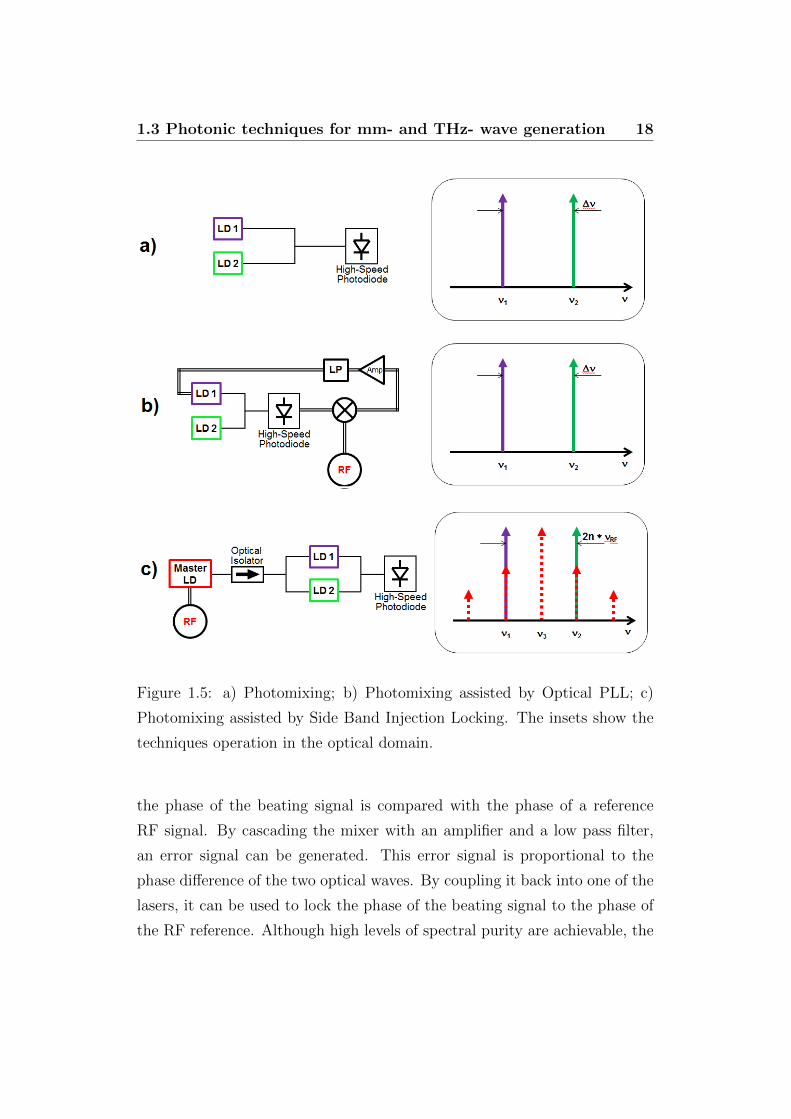
1.3 Photonic techniques for mm- and THz- wave generation 18
Figure 1.5: a) Photomixing; b) Photomixing assisted by Optical PLL; c)
Photomixing assisted by Side Band Injection Locking. The insets show the
techniques operation in the optical domain.
the phase of the beating signal is compared with the phase of a reference
RF signal. By cascading the mixer with an amplifier and a low pass filter,
an error signal can be generated. This error signal is proportional to the
phase difference of the two optical waves. By coupling it back into one of the
lasers, it can be used to lock the phase of the beating signal to the phase of
the RF reference. Although high levels of spectral purity are achievable, the

1.4 Photomixing assisted by mutual injection locking and FourWave Mixing 19
complexity of the system makes it impossible to be integrated into a single
monolithic chip. Not only a RF seed signal is required, but also electronic
mixer and amplifier have to be used. Moreover, the presence of electronic
components limits the tunability of the generated signal, making the THz-
range difficult to achieve.
In the Photomixing assisted by Side Band Injection Locking the two free
running lasers (ν1 and ν2) are phase locked by the injection of a third laser
(ν3) [33–35]. The additional master laser is directly modulated by a RF seed
signal at the frequency νRF (Figure 1.5c). The applied modulation creates
several sidebands around the central frequency of the master laser. Each
sideband is located at the frequency ν3± n · νRF , where n is the order of the
sidebands. The master laser is then injected into the two free running lasers.
By choosing the wavelengths of the two slave lasers to be ν1 = ν3 − n · νRFand ν2 = ν3 + n · νRF , they can be injection locked by the nth sidebands
of the master laser. Their beating on a high speed photodiode produces
a spectrally pure signal. However, also in this case the spectral purity is
achieved at the expense of an external RF seed signal. The need for the
external RF signal prevents the system from being integrated into a single
monolithic chip, offering a limited tunability of the generated mm- wave
signal and making the THz- range not achievable.
Although all the techniques so far described are very promising and used in
different applications, they do not satisfy the requirements of integrability,
tunability and spectral purity at the same time.
1.4 Photomixing assisted by mutual injection
locking and Four Wave Mixing
An alternative improvement of the photomixing technique has been re-
cently proposed [1], based on the Photomixing assisted by mutual injection
locking and Four Wave Mixing. Previous experiments demonstrated the ca-
pability of this technique of satisfying all the discussed requirements. This

1.4 Photomixing assisted by mutual injection locking and FourWave Mixing 20
technique is a further improvement of the photomixing techniques previously
described. It is based on an all-optical phase locking of three single mode
lasers, and it allows to achieve wide tunability and high spectral purity of
the photomixing signal, without the need for an external spectrally pure RF
seed signal. The simultaneous locking of three lasers is achieved via the sum
of two locking effects: mutual injection locking and injection locking assisted
by Four Wave Mixing (FWM).
The description of the locking mechanism can start from considering two
mutually optically coupled single mode lasers, operating at two distinct fre-
quencies ν1 and ν2 (Figure 1.6).
Figure 1.6: Mutual injection locking through modulation sidebands.
In each laser diode, the carrier density is sinusoidally modulated in time at
the beating frequency ν12 = |ν1−ν2|. As consequence, modulation sidebands
arise on both upper and lower sides of the optical carrier generated by each
laser, specifically at frequencies ν = ν1 ± ν12 inside the laser 1 and ν =
ν2 ± ν12 inside the laser 2. Due to the mutual injection configuration, the
two lasers can exchange their phase information through these modulation
sidebands, achieving a stable reciprocal phase relation. Therefore, as already
demonstrated in [36], the two lasers can be phase locked through their self-
produced modulation sidebands. However, this situation does not ensure
the stability of their lasing frequencies, since the sidebands are generated
(and mutually injected) whatever is the instantaneous frequency separation

1.4 Photomixing assisted by mutual injection locking and FourWave Mixing 21
between the lasers. The beating of the two lasers on a photodiode would
exhibit only a very small improvement from the basic photomixing technique,
preventing from the generation of a spectrally pure RF signal.
An improved frequency stability of the system can be achieved by introducing
a feedback effect on the instantaneous emission frequencies of the lasers. This
can be done by adding to the previously described configuration a third laser,
operating at the frequency ν3, as show in Figure 1.7.
Figure 1.7: Mutual injection locking assisted by Four Wave Mixing. The
colour of the FWM clones in the figure indicates the lasers which interaction
generated each clone.
In the new configuration laser 1 and laser 2 are injected into a third laser,
placed between them. Both the laser pairs 1 - 3 and 2 - 3 are mutually
coupled. Moreover, a FWM process takes place inside the laser 3, producing

1.4 Photomixing assisted by mutual injection locking and FourWave Mixing 22
two clones of the injected lasers 1 and 2, respectively at the frequencies
ν ′1 = 2ν3 − ν1 and ν ′2 = 2ν3 − ν2. When the laser 3 is operating at the
frequency
ν3 =ν1 + ν2
2(1.3)
a double locking mechanism occurs. First of all, the lasers 1 and 2 phase
lock to laser 3 thanks to the sideband locking mechanism already described.
Secondly, the FWM clones ν ′1 and ν ′2 have respectively frequencies ν ′1 = ν2
and ν ′2 = ν1. Due to the mutually coupled configuration, these FWM clones
generated inside laser 3 are injected into lasers 1 and 2, thus locking their
instantaneous frequency difference.
Figure 1.8: Mutual injection locking assisted by Four Wave Mixing, with the
full mutual locking mechanism illustrated.
As shown in Figure 1.8, the three lasers now constitute a three coupled
oscillators system, where all the oscillators are coupled to the others. The
lasers pairs 1 - 3 and 2 - 3 are coupled through their modulation sidebands,
while the laser pair 1 - 2 is coupled by the FWM process that takes place
in laser 3. This multiple locking mechanism ensures an improved stability

1.4 Photomixing assisted by mutual injection locking and FourWave Mixing 23
of the system, locking the frequency difference between the lasers. There-
fore, when the locking condition represented by the Eq. (1.3) is satisfied,
the electrical beating signal generated by photomixing on a high speed pho-
todiode is expected to exhibit improved spectral characteristics. The FWM
process represents the most convenient way to lock lasers operating at dif-
ferent frequencies, thanks to its capability to generate optical modes at new
frequencies.
This recently proposed technique is potentially capable to satisfy all the dis-
cussed requirements. Thanks to the all-optical locking method, this system
can produce spectrally pure photomixing signals without the need of an ex-
ternal RF seed signal. By increasing the frequency spacing between the lasers
(while satisfying the locking condition), the generated RF signal can also be
widely tuned from a few GHz up to the THz domain, thanks to the high
efficiency of the FWM process. As reported in [37], in semiconductor medi-
ums the FWM for detuning values larger than a few tens of GHz is due to
the spectral hole burning, which acts as non-linear suppression of the opti-
cal gain. The spectral hole burning is governed by the intraband relaxation
processes, which can be extremely fast, in order of less than a picosecond.
As consequence the FWM process can take place for pump-probe detuning
up to ∼1 THz. However, at large detuning the FWM efficiency decreases
[37], and consequently higher level of optical power have to be injected into
laser 3. For small detunings, the FWM process is very efficient, and therefore
an attenuation between the lasers is necessary in order to avoid an unsta-
ble regime of operation of the injected laser. On the other hand, for large
detuning the FWM efficiency strongly decreases, requiring lower level of at-
tenuation or even the amplification of the FWM clones.
Experiments using a setup with discrete components have been previously
carried out [1]. Figure 1.9 shows the experimental setup used to demon-
strate the mutual locking, where three DFB lasers without optical isolator
were mutually injected through optical fibres.
DFB-1 and DFB-2 were mutually coupled with DFB-3, where the FWM

1.4 Photomixing assisted by mutual injection locking and FourWave Mixing 24
Figure 1.9: Experimental discrete setup for the mutual injection locking
assisted by FWM.
process took place. The clones generated inside the DFB-3 cavity were then
back injected to the lasers 1 and 2 following a different path, in order to
allow a better control on the injection levels. Attenuators were inserted, to
adjust the injection levels and avoid unwanted complex dynamic regimes of
operation. Moreover, the attenuators prevented from a strong self optical
feedback the may be generated from the amplification of each laser when
injected into the others.
Promising experimental results were obtained, achieving stable locking for
detuning up to 100 GHz. However, excessive optical feedback from the var-
ious optical fibre components leaded to a narrowing of the laser linewidths
with respect to the ideal unperturbed case. As consequence, the linewidth
and phase noise of the beating RF signal could not be measured reliably.
In order to assess the phase noise reduction, additional drive-current noise
was applied to one of the lasers. Figure 1.10 shows the RF beating when the
three lasers are unlocked and locked.
A clear suppression of the noise was achieved, thanks to the mutual injec-
tion locking mechanism that strongly enhanced the stability of the system.
Since no external RF signal was used to lock the lasers, this all-optical lock-
ing technique had the potential to be fully integrated into a single monolithic
device. The aim of this work was the integration of the hybrid setup previ-
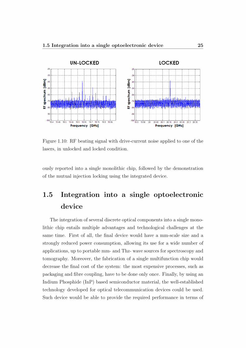
1.5 Integration into a single optoelectronic device 25
Figure 1.10: RF beating signal with drive-current noise applied to one of the
lasers, in unlocked and locked condition.
ously reported into a single monolithic chip, followed by the demonstration
of the mutual injection locking using the integrated device.
1.5 Integration into a single optoelectronic
device
The integration of several discrete optical components into a single mono-
lithic chip entails multiple advantages and technological challenges at the
same time. First of all, the final device would have a mm-scale size and a
strongly reduced power consumption, allowing its use for a wide number of
applications, up to portable mm- and Thz- wave sources for spectroscopy and
tomography. Moreover, the fabrication of a single multifunction chip would
decrease the final cost of the system: the most expensive processes, such as
packaging and fibre coupling, have to be done only once. Finally, by using an
Indium Phosphide (InP) based semiconductor material, the well-established
technology developed for optical telecommunication devices could be used.
Such device would be able to provide the required performance in terms of

1.5 Integration into a single optoelectronic device 26
frequency stability, tunability, efficiency and reliability.
At the same time, the monolithic integration of different optical devices
brings several technological and design challenges. The fabrication process
have to be optimised in order to define all the different optical structures in
few lithography steps. The use of a post-growth fabrication process would
be preferable, since a material regrowth would increase the fabrication com-
plexity and costs, decreasing at the same time the final yield of the working
devices. The yield is particularly important in complex multi-section devices,
since their correct operation is achieved only when all the optical structures
of the device are fully working. Finally, the mutual injection of lasers may
lead to unstable or chaotic regimes of operation if the injection levels are
not optimised. Complex multi-section devices have to be designed, where
attenuators and couplers have to be fully integrated with the lasers. Due to
the complexity of the mutual injection scheme, different geometries, coupling
and attenuation levels have to be investigated in order to find out the best
design solution.

Chapter 2
Device Design
This chapter details the design of the monolithic devices where the mu-
tual injection locking of three lasers is exploited, aiming at the generation
of mm-waves. Different geometries were investigated, requiring the dedi-
cated design of several optical structures. First of all, the different device
geometries are presented, describing their operating principle. The chapter
continues with the detailed description of the semiconductor material that
will be used to fabricate the devices, since the layout of each optical structure
strongly depends from its characteristics. Then the design of each compo-
nent is detailed: the waveguides are firstly introduced, also describing their
utilisation as integrated spot size converters. A complete analysis of the
Distributed FeedBack (DFB) lasers follows, starting from the mathematical
theory used to model their behaviour, to the design choices that have been
made in order to guarantee single mode operation and precise determination
of the lasing wavelength. Finally, the chapter closes with the design of the
different optical couplers used in the devices. It will be also shown the im-
portance of properly taking into account the fabrication limits and tolerances
during the design stage, in order to define structures that can be fabricated
obtaining a high yield.

2.1 Device geometries 28
2.1 Device geometries
As described in the previous chapter, three lasers can be phase-locked via
mutual injection assisted by a Four Wave Mixing process. When appropriate
locking conditions are satisfied (Figure 2.1a), the beating of the locked lasers
on a high-speed photodiode generates spectrally pure mm-waves. Since this
method does not require the use of any RF seed signal, it can be fully inte-
grated on a single optoelectronic device.
The mutual injection locking at different frequencies is ensured by the genera-
tion of optical clones at new frequencies, followed by a subsequent re-injection
of these new signals back into the original optical sources. Therefore, the in-
tegrated devices required three fundamental elements:
• Three single mode lasers operating at the frequencies ν1, ν2 ν3
• A non-linear section where the two Four Wave Mixing clone signals can
be generated
• A feedback mechanism to allow the re-injection of the newly generated
clone signals into the original lasers.
Starting from these fundamental elements, different geometries were con-
ceived and investigated (see Figure 2.1b).
As single mode sources, DFB lasers represented the best option. Thanks
to a very flexible design of their optical properties (Section 2.4), they can
stably operate in a single-mode regime with high SMSR and precisely de-
fined lasing wavelength.
The Designs 1, 2, 3 share the same principle of operation. DFB-1 (oper-
ating at ν1) and DFB-2 (ν2) are coupled into DFB-3 (ν3), where, due to
the high non-linearity of the active material, Four Waves Mixing clones at
the idler frequencies ν ′1 and ν ′2 are generated. The DFB-3 also provide the
feedback mechanism necessary for the mutual locking, by reflecting back /
transmitting the newly generated clones towards the original lasers. The new
optical frequencies are generated into the cavity of DFB-3, where they also

2.1 Device geometries 29
Figure 2.1: a) Mutual injection scheme. b) Conceptual scheme of the different
device geometries investigated.

2.1 Device geometries 30
get amplified thanks to the active cavity resonance. The signals are finally
re-emitted from DFB-3, and coupled back to the DFB-1 and DFB-2 through
an optical coupler.
Design 1, 2, 3 differ for the coupling strength between the lasers. It is
highly important that this aspect be investigated, because the locking prop-
erties of mutually injected lasers strongly depend on the strength of their
mutual coupling. High levels of injected power might lead to an unwanted
unstable regime of operation. On the other hand, too low levels of injection
might be not sufficient to ensure the locking between the lasers. In order to
gain more insight into this issue, in Design 1 evanescent couplers are used to
couple low levels of power: a value of 1% was chosen. In Design 2 a Multi
Mode Interference coupler is used to achieve a coupling of 50% with a short
coupler. In Sections 2.5 the design of these couplers is discussed. Finally,
in Design 3 the lasers are coupled through direct injection, with a coupling
factor of 100%. The yellow sections in Figure 2.1b represent optically active
waveguides, which can be used as Semiconductor Optical Amplifiers (SOA)
or as attenuator, depending on whether they are operated under direct or
reverse bias respectively. These sections can be used to further adjust the
injection levels of optical power.
Design 4 strongly differs from the previous ones. The three single mode
lasers are injected through a MMI coupler into an auxiliary non-linear active
section, where the Four Wave Mixing process occurs. The optical signals
are then reflected by a straight-cleaved facet at the edge of the device. The
semiconductor-air interface reflects 30% of the incident optical power, thus
providing the feedback mechanism. The reflected signals are further ampli-
fied during the second transit through the SOA, and finally injected in the
DFB lasers.
Besides the mentioned optical structures, single mode waveguides were used
to distribute the optical signals along the chip. Tilted and tapered output
waveguides were used to collect the generated optical signals using lensed
optical fibres. Finally, inverse tapered waveguides were used in Design 1 to

2.2 Material description 31
disperse the uncoupled light, avoiding backreflections that could negatively
affect the proper operation of the device. The waveguide design is discussed
in Section 2.3.
2.2 Material description
The device design starts from the study of the semiconductor material
that will be used for the fabrication. The design is strongly related to the
material, since different compounds have different layer structures and opti-
cal characteristics (refractive index, gain spectrum, etc.), according to which
the geometrical characteristics of the devices have to be varied. The pho-
tomixing effect used to generate the mm-waves works on the frequency differ-
ence between the optical signals rather than their absolute frequency. This
makes every optically active semiconductor suitable for the fabrication of the
devices. However, the choice fell on a material with a gain spectrum cen-
tred around the C-band wavelength range (1530-1565 nm), normally used
for telecommunications devices. This choice is mainly due to the maturity of
the growth techniques used for producing such material and also to the avail-
ability of a wide range of instruments to characterise the devices. Moreover,
state-of-the-art fabrication techniques for this material were available in the
institution chosen for the fabrication of the devices (described in Chapter 3).
The material used is a commercially available1 AlGaInAs/InP compound,
with a multiple quantum well (MQW) structure. Figure 2.2 shows the struc-
ture of the epitaxial wafer.
Recently, several theoretical and experimental studies focussed on the
Al-quaternary material, due to its attractive band discontinuity properties.
It was shown that the conduction band offset of AlGaInAs/InP material
(∆Ec=0.72∆Eg) is larger compared to that of the traditional InGaAsP/InP
material (∆Ec=0.40∆Eg), leading to improved electron confinement and
higher characteristic temperature [38–40].
1IQE Ltd, Cardiff, U.K. (www.iqep.com)

2.2 Material description 32
200 nm GaInAs cap
60 nm AlGaInAs
1720 nm InP cladding
60 nm AlGaInAs GRINSCH
MQW and barriers
60 nm AlGaInAs GRINSCH 60 nm AlGaInAs
800 nm InP cladding
n-type InP substrate
Waveguide core
Figure 2.2: Layer structure of the commercial material IQE-IEGENS-13-17,
used for the fabrication of the devices.
The material was grown by Metal Organic Chemical Vapour Deposition
(MOCVD), and consists of five compressively strained (12000 ppm) 6nm
thick Al0.07Ga0.22In0.71As wells with six tensiley strained (-3000 ppm) 10nm
thick Al0.224Ga0.286In0.71As barriers. The QWs and barriers are situated be-
tween two 60nm AlGaInAs graded index separate confinement heterostruc-
ture (GRINSCH, GRaded INdex Separate Confinement Heterostructure) lay-
ers. The GRINSCH section is included to prevent electrons and holes from
escaping the QW region. Moreover, it allows for a lower threshold current
density and larger differential gain as compared to standard SCH structures
[41]. Finally, the structure is completed by an 800nm InP lower cladding,
1720nm InP upper cladding and a 200nm highly doped (1.5 x 1019cm−3)
GaInAs contact layer. All layers (except the wells and barriers) are lattice
matched to a n-doped InP substrate with Zn and Si used as the p-type and
n-type dopants respectively.

2.3 Waveguides 33
2.3 Waveguides
The described layer structure ensures the photon confinement in the ver-
tical direction, since the core’s refractive index is higher than that of the top
and bottom cladding layers. However, in order to achieve the guiding effect,
lateral confinement of photons is also needed. This is provided by etched
ridge waveguide technique that produces lateral index guiding and transver-
sal current confinement. There are two commonly used structures for achiev-
ing such index guiding: shallow-etched and deep-etched ridge waveguides, as
shown in Figure 2.3.
Figure 2.3: Schematic of a shallow etched and a deep etched waveguides.
The shallow-etched waveguides are defined by etching the ridge down to
the upper edge of the active region, but not through it. They ensure a rel-
atively low lateral photon confinement, since the effective refractive index
difference (∆neff = neff - nc) between the non etched and etched areas is
small, typically smaller than 0.1. However, the amount of lateral confine-
ment is large enough to fabricate waveguides which sustain a single transver-
sal mode, and becomes problematic only for curved waveguides with small
radius. On the other hand, as the etching does not penetrate into the core,
the shallow-etched waveguides provide a reduced carrier recombination rate
at the sidewall, and the sidewall roughness induces negligible back-reflections
because the optical mode does not overlap with the ridge sidewall regions.
Deep-etched waveguides are defined by etching the ridge down through the

2.3 Waveguides 34
core. They ensure a stronger lateral confinement of the optical mode, as there
is a much larger difference between the refractive indices of the waveguide and
the surrounding medium (usually air). This allows the fabrication of low-loss
curved waveguides with a small radius. However, the increased interaction
of the optical mode with sidewalls may lead to large back-reflections and
scattering losses if the sidewall roughness is not sufficiently small. Moreover,
non-radiative recombination is more likely to occur since the quantum wells
are exposed to the atmosphere. This might lead to the generation of phonons
and heating, negatively affecting device performance and lifetime.
For the above reasons, the shallow-etch approach was chosen for the fabri-
cation of the optical structures; this approach requires the material to be
etched down for 1920 nm, i.e. until the first Al-containing layer placed at the
top edge of the core is reached. Moreover, as it will be widely discussed in the
next chapter, the Al-containing layer may be used as a dry etch stop layer,
allowing a very precise and repeatable definition of the optical structures.
The number of the guided TE polarised modes depends on the waveguide
width. In order to guide only the fundamental TE mode, it is necessary to
determine the waveguide width below which the higher order modes are sup-
pressed. A set of simulations was carried out using the commercial software
RSoft BeamPropTM, based on the beam propagation method (BPM). The
refractive indices of the different layers were calculated using [42] and the
dedicated website Luxpop2. The results indicated that, for waveguide width
of 2.6 µm and below, only the fundamental mode is supported. A value of 2
µm was then chosen, in order to increase the losses of the non-fundamental
modes and avoid any power transfer to them. Figure 2.4 shows the simulated
optical field density of a 2 µm width waveguide, etched down till the edge of
the active layers (etch depth of 1920 nm); the dashed lines reveal the position
of the core inside the material.
As shown in Figure 2.1, the devices require also curved waveguides. The
shallow etched ridges are able to effectively guide the optical mode also for
2www.luxpop.com

2.3 Waveguides 35
Figure 2.4: Simulated optical field density of a 2 µm width and 1920 height
ridge; the solid line represents the etched ridge profile, while the dashed lines
underline the position of the core inside the material.
curved guides, as long as the radius of curvature is larger than a certain
value. Extensive studies on this material were previously carried out, while
aiming the fabrication of ring and micro-ring lasers for all-optical process-
ing3 [43, 44]. Using this material, it was shown that a curved shallow etched
ridge waveguide 2 µm wide and 1920 high exhibits negligible curvature losses
provided the bend radius larger than 250 µm. Therefore, all the curved
waveguides used in the devices had a radius of curvature of 300 µm.
Some considerations are due about the output waveguides. Proper operation
of the devices requires low back-reflection from the output cleaved facets, in
order to not spoil the single mode operation of the DFBs (Section 2.4) and
to avoid the creation of sub Fabry-Perot/etalon cavities. There are two well
known methods to reduce reflections of a cleaved facet: the application of
an antireflection (AR) coating and the tilting of the ouput waveguides with
respect to the cleaving plane. AR requires the deposition of a multilayer thin
3www.iolos.org
2.3 Waveguides 36
film on the facet, where the semiconductor-air interface creates the backre-
flections. The refractive index and thickness of these layers has to be accu-
rately designed to produce destructive interference in the light reflected from
the interfaces, and constructive interference in the corresponding transmitted
light. However, in order to not add further fabrication steps, the tilting of
the output waveguides was preferred. With this method the reflected power
coupled back to the waveguide can be strongly reduced, although the reflec-
tivity at the interface does not change significantly. Marcuse in [45] shows
that the reflected power already decreases of 25 dB by tilting the output
waveguides by an angle of only 5 degrees. Larger angles provide even lower
backreflections, but the wide refraction angle of the free space beam may
make the light collection troublesome. A trade-off was found by tilting the
output waveguides 10: this produces a transmission angle of 33.
A further improvement of the output waveguides was made in order to max-
imise the coupling efficiency between the chip and the lensed fibre. The idea
was to create an integrated spot-size converter, which adiabatically trans-
forms the waveguide mode and reduces the modal mismatch with the lensed
fibre. This was easily done by up-tapering the output waveguides from the
standard width of 2 µm to 12 µm. This transformation occurs over a length
of 100 µm. The modal spot was optimised aiming an efficient coupling with
the available lensed fibre4. The use of tapered output waveguides also im-
proves the alignment tolerances and, in case of tilted waveguides, it further
reduces the back coupled optical power [45].
Finally, down-tapered waveguides were also used. The Design 1 requires only
a small amount of optical power to be coupled between the different lasers.
The uncoupled power has to be dispersed in order to avoid back reflections
and/or subsequent coupling with other waveguides. By down-tapering the
standard 2 µm waveguide to a nanometer-sized tip, the propagating mode is
pushed down into the substrate where it is scattered away due to the absence
of a guiding structure. The smooth down-shift of the mode ensures very low
4OZ optics TSMJ-3A-1550-9/125-0.25-7-5-26-2-AR
2.4 DFB design 37
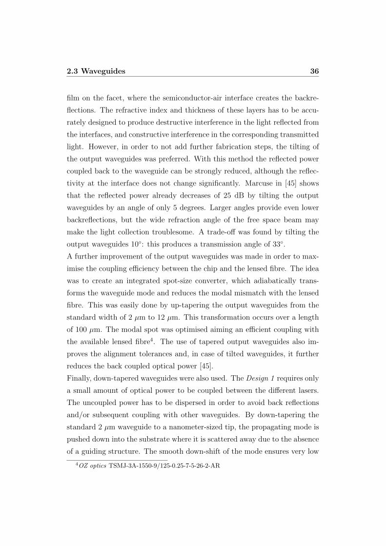
back reflections of optical power. Figure 2.5 shows how the inverse taper
spreads the mode into the substrate.
Figure 2.5: Propagating mode is dispersed into the substrate by down-
tapering the standard 2 µm waveguide down to a nanometer-sized tip.
2.4 DFB design
The DFB lasers represent the core of the devices, where the optical signals
are generated. As discussed in the previous chapter, the mutual injection-
locking assisted by FWM requires single mode lasers, with high SMSR.
A conventional Fabry-Perot laser exhibits multiple longitudinal modes be-
cause the reflectivity of its mirrors is not wavelength-selective, and conse-
quently a large number of modes are close or above the lasing threshold.
The most common way to achieve single mode operation in integrated lasers
is the use of periodic structures such as Bragg gratings. They act as mir-
rors with a wavelength-dependent reflectivity, increasing the gain difference
between the dominant mode and the side modes. In this section, the theory
behind the Bragg reflectors is briefly reviewed; different design solutions will
2.4 DFB design 38
be discussed in order to fabricate DFB lasers which operate in a single mode
regime and with a well defined and predictable lasing wavelength.
2.4.1 Coupled-wave equations
As discovered by W.L. Bragg [46], it is possible to induce coupling be-
tween orthogonal modes of a waveguide by introducing a refractive index
perturbation; by making this perturbation periodic in the propagating direc-
tion, the forward and backward propagating modes of the waveguide can be
coupled. This effect, known as backward Bragg scattering, produces coherent
coupling only between fields that propagate at specific wavelengths, defined
by the Bragg condition:
mλb = 2neffΛ0 (2.1)
where m is the order of the grating response, λb is the free space wavelength
of the mode satisfying the Bragg condition, neff is the effective index of the
relevant waveguide mode and Λ0 is the grating period.
The effects of this refractive index perturbation over the fields involved have
been studied in several papers and books [47–51]. They can be described
starting from the general wave equation for the electric field propagating
with a wavelength λb and free space propagation constant k0 = 2π/λb:
d2E
dz2+ β2
0E = 0 (2.2)
where E is given by the sum of the forward and backward propagating fields
and β0 = n(z)k0 is the Bragg propagation constant, with n(z) the refractive
index along the propagating direction. The general solution can be written
in the form:
E(z) = R(z)e(−jβ0z) + S(z)e(jβ0z) (2.3)
where the electric filed is described as sum of right- and left- propagating
2.4 DFB design 39
fields. The functions R(z) and S(z) vary comparatively slow with z because
the rapidly varying phase factor is included in the exponential functions. By
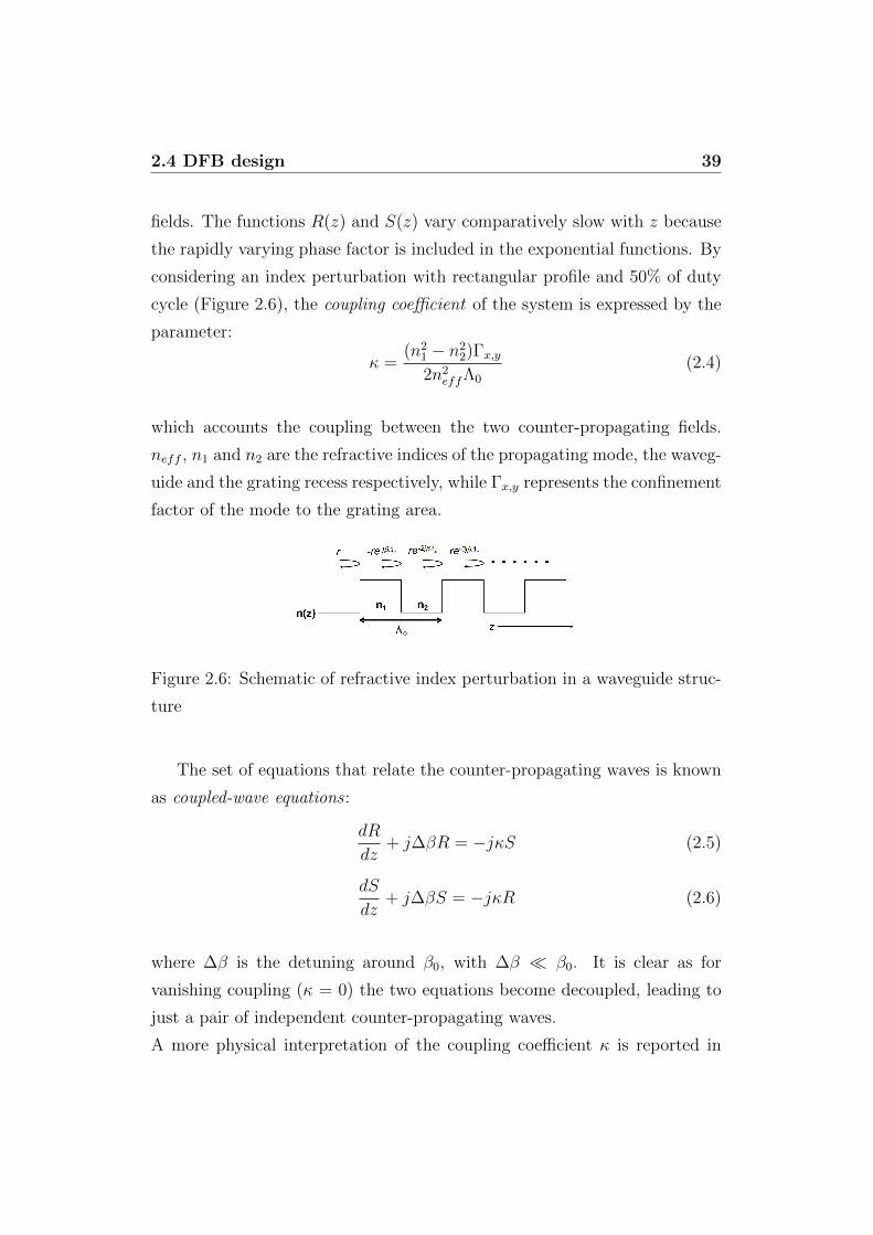
considering an index perturbation with rectangular profile and 50% of duty
cycle (Figure 2.6), the coupling coefficient of the system is expressed by the
parameter:
κ =(n2
1 − n22)Γx,y
2n2effΛ0
(2.4)
which accounts the coupling between the two counter-propagating fields.
neff , n1 and n2 are the refractive indices of the propagating mode, the waveg-
uide and the grating recess respectively, while Γx,y represents the confinement
factor of the mode to the grating area.
Figure 2.6: Schematic of refractive index perturbation in a waveguide struc-
ture
The set of equations that relate the counter-propagating waves is known
as coupled-wave equations :
dR
dz+ j∆βR = −jκS (2.5)
dS
dz+ j∆βS = −jκR (2.6)
where ∆β is the detuning around β0, with ∆β β0. It is clear as for
vanishing coupling (κ = 0) the two equations become decoupled, leading to
just a pair of independent counter-propagating waves.
A more physical interpretation of the coupling coefficient κ is reported in

2.4 DFB design 40
[48]. By considering the periodic structure shown in Figure 2.6, the field
reflection coefficient r of the first discontinuity follows the Fresnel formula:
r =∆n
2neff(2.7)
where ∆n = n1−n2. The field reflection of the next discontinuity is -r because
now the field goes from a high to a low index. When the wavelength is equal
to the Bragg wavelength, the phase change for a round-trip in a subsection
is β0Λ0 = π, corresponding to a factor -1. Therefore, all reflections add
in phase, and the field reflectivity per unit length (with two reflections per
period) is:
κ =2r
Λ0
=∆n
neff
2neffλb
=2∆n
λb(2.8)
giving a clear idea that the coupling coefficient of a periodic structure can
be interpreted as the amount of reflection per unit length.
By knowing the functions R and S at a given point, for example z = 0, the
general solution of the coupled-wave equations can be written as [48]:
R(z) =
[cosh(γz)− j∆β
γsinh(γz)
]R(0)− jκ
γsinh(γz)S(0) (2.9)
S(z) =jκ
γsinh(γz)R(0) +
[cosh(γz) +
j∆β
γsinh(γz)
]S(0) (2.10)
where γ2 = κ2−∆β2. The solutions given in (2.9) and (2.10) can be written
in a matrix form: [R(z)
S(z)
]= M(z)
[R(0)
S(0)
](2.11)
where M(z) is:
M(z) =
(cosh(γz)− j∆β
γsinh(γz) − jκ
γsinh(γz)
jκγsinh(γz) cosh(γz) + j∆β
γsinh(γz)
)(2.12)

2.4 DFB design 41
In the literature, the Bragg laser analysis is often carried out by using the
transfer matrix theory, since it represents a powerful tool to model grating
lasers as well as for structures consisting of several different periodic sections
in the longitudinal direction.
2.4.2 Grating design
The coupled-wave equations give the mathematical tool to design a Bragg
grating as a wavelength-dependent mirror. The design starts by choosing
the Bragg wavelength of the grating, followed by the design of its reflectivity
spectrum.
From (2.1), the Bragg wavelength λb is designed by varying the grating period
Λ0 and the grating order m; the minor effects of a neff variation will be
described in Section 2.4.4. A period Λ0 of 242 nm was chosen in order to
target the gain peak of the available semiconductor material (centred around
1550 nm), considering a first order grating with a neff ' 3.20. By defining
an index profile as shown in Figure 2.6, the first order grating with 50% of
duty cycle D is the one that gives the highest coupling coefficient. For other
grating shapes or orders the coupling coefficient has to be reduced as follow
[48]:
κ(mth−order) = κ(1st−order) · fred (2.13)
with:
fred =1
m· |sin(πmD)| (2.14)
Figure 2.7 shows the effect of (2.14).
The first order not only allows the highest coupling factor for a given
index profile, but it also ensures the smallest dependence of κ on the duty

2.4 DFB design 42
Figure 2.7: Reduction factor fred as a function of duty cycle D, for different
grating orders m.
cycle. This is important in order to minimise the fabrication tolerances when
defining the index profile.
The second design step is the definition of the reflectivity spectrum of the
grating. The key spectrum properties that can be designed are the width of
the reflectivity spectrum ( also called stop band of the grating) and the peak
of reflectivity at the Bragg wavelength. From the coupled-wave equations
(2.9) and (2.10), and considering ∆β =2πneff
λ− 2πneff
λband γ2 = κ2 −∆β2,
the behaviour of a Bragg grating as a wavelength-dependent reflector can be
described by its power reflectivity R(λ) [48]:
R(λ) =κ2sinh2(γL)
∆β2sinh2(γL) + γ2cosh2(γL)(2.15)
It is clear that the spectral properties of the grating strongly depend on the
coupling coefficient κ and interaction length L (which represents the grating
length). It is interesting to investigate how κ and L can affect the reflectivity
spectrum. Figure 2.8 shows the reflectivity spectrum as a function of λ, for
different coupling coefficients κ and interaction lengths L. It appears that
when κ increases, both the stop band width and reflectivity peak at λ = λb

2.4 DFB design 43
Figure 2.8: Reflectivity spectrum Vs wavelength for different grating lengths
(a,c) and coupling coefficient (b,d).
increase, up to saturate at R = 1 for a wide range of wavelengths. On the
other hand, when the grating length L increases the stop band narrows, while
the reflectivity increases. This can be simply summarised as:
κ ⇑ −→ StopBand ⇑, Reflectivity ⇑
L ⇑ −→ StopBand ⇓, Reflectivity ⇑
By increasing κ, the coupling between the counter-propagating modes in-
creases, thus the grating is able to couple light at sitting further from the

2.4 DFB design 44
Bragg wavelength. By increasing the length L, more grating periods partici-
pate in the backward Bragg scattering, enhancing the wavelength selectivity
of the grating.
The stop band can be conveniently defined as the separation in wavelength
between the first two zeros of the reflectivity spectrum. From (2.15), it is
readily found that (for ∆βL > κL) the first zeroes of R are found as:
∆βL =√
(κL)2 + (π)2 (2.16)
Moreover, again from (2.15), the power reflectivity for λ = λb reduces to:
R = tanh2(κL) (2.17)
From (2.16) and (2.17), Figure 2.9 shows how the stop band width and
reflectivity peak depend on the coupling coefficient κ and grating length
L. The graphical visualisation of the relations between κ and L and the
grating properties represents a very powerful tool when designing gratings
with precise requirements of stop band width and reflectivity at the same
time. It shows how different combinations of coupling coefficient and grating
length give the same stop band width, allowing a free choice of their values
in order to ensures the required reflectivity.
Equation (2.17) shows that the magnitude of reflection at λb is determined
only by the κL product. This dimensionless parameter, known as normalised
coupling coefficient κL, determines the performances of the whole grating,
allowing the generalisation of the results for gratings with different coupling
coefficients and lengths. Figure 2.10 shows the curve describing the peak
power reflectivity R(λb) as a function of κL.
As it will be described in Chapter 4, some preliminary tests were per-
formed in order to find out the value of κL that ensures the best characteris-
tics for the DFB lasers in terms of threshold current and SMSR. Satisfactory
results were obtained by fabricating 400 µm long gratings with a κ of 75

2.4 DFB design 45
Figure 2.9: Stop band width and reflectivity peak as a function of the cou-
pling coefficient κ and grating length L.
Figure 2.10: Peak power reflectivity R(λb) as a function of κL.

2.4 DFB design 46
cm−1, which gives κL = 3. These values ensure a stop band of about 3 nm
and a reflectivity close to unity.
2.4.3 DFB for single mode operation
The analysis carried out so far did not take into account the gain of the
material. Depending on the relative position of active region and grating,
different types of lasers can be obtained. In a Distributed Bragg Reflector
(DBR) lasers the active region and the grating are separated longitudinally.
The mathematical analysis can be carried out using the equations previously
reported, since the grating acts as a passive wavelength selective reflector. In
a Distributed FeedBack (DFB) laser the grating is superimposed on the active
region, combining the grating reflection with the optical amplification in the
same volume. Historically, DFB lasers preceded the development of DBRs,
mainly because DFBs are easier to fabricate, since no longitudinal integration
of active and passive region is required. However, the mathematical analysis
of DFBs is slightly more complicated, since the gain and phase conditions
cannot be separated.
The simplest DFB structure is formed by a grating defined just below or
above the active material, and by neglecting Fabry-Perot reflections arising
from the end facets. The analysis of this structure can still be based on the
coupled-wave equations (2.9 and 2.10), but the gain has to be considered by
replacing ∆β with (∆β+jg0), where g0 represents the gain for the field. The
intensity gain is represented by 2g0. As discussed in [47–49], the oscillation
condition is found by taking into account the boundary conditions for the
system. This devices differ from the normal Fabry-Perot cavities, where the
boundary conditions for internal waves are determined by outcoming waves,
incident onto the mirrors. A distributed feedback structure represents a self-
oscillating system: as shown in Figure 2.11, the internal waves start from
zero amplitude at the boundaries, receiving their energy via scattering from
the counter-propagating waves.
From this observation, the boundary conditions S(0) = R(L) = 0 fol-

2.4 DFB design 47
Figure 2.11: a) Laser oscillation in a periodic structure. b) Plot of the am-
plitudes of left travelling wave (S) and right travelling wave (R) Vs distance.
Image from [47]
.
low, where L represents the grating length. Considering the coupled-wave
equations written with the matrix formalism (2.11), the boundary conditions
require the term M22 to be set at zero:
cosh(γL) +j(∆β + jg0)
γsinh(γL) = 0 (2.18)
where the parameter:
γ2 = κ2 − (∆β + jg0)2 (2.19)
now includes the gain. Re-writing the oscillation condition (2.18) as:
γLcoth(γL) = −j(∆βL+ jg0L) (2.20)
a complex transcendental equation is obtained. It determines, for a given
product κL, the possible values of (∆βL, g0L). Each solution gives the wave-
length (in terms of ∆β) and the required threshold gain (in terms of g0) for
the possible lasing modes. It is clear how, in contrast to the situation for
Fabry-Perot or DBR lasers, the gain and phase conditions do not separate
but are determined together from the complex number (∆βL+ jg0L) [48].
2.4 DFB design 48
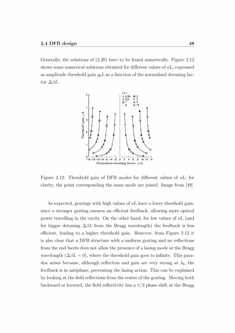
Generally, the solutions of (2.20) have to be found numerically. Figure 2.12
shows some numerical solutions obtained for different values of κL, expressed
as amplitude threshold gain g0L as a function of the normalised detuning fac-
tor ∆βL.
Figure 2.12: Threshold gain of DFB modes for different values of κL; for
clarity, the point corresponding the same mode are joined. Image from [49]
As expected, gratings with high values of κL have a lower threshold gain,
since a stronger grating ensures an efficient feedback, allowing more optical
power travelling in the cavity. On the other hand, for low values of κL (and
for bigger detuning ∆βL from the Bragg wavelength) the feedback is less
efficient, leading to a higher threshold gain. However, from Figure 2.12 it
is also clear that a DFB structure with a uniform grating and no reflections
from the end facets does not allow the presence of a lasing mode at the Bragg
wavelength (∆βL = 0), where the threshold gain goes to infinity. This para-
dox arises because, although reflection and gain are very strong at λb, the
feedback is in antiphase, preventing the lasing action. This can be explained
by looking at the field reflections from the centre of the grating. Moving both
backward or forward, the field reflectivity has a π/2 phase shift at the Bragg

2.4 DFB design 49
wavelength. This entails a total round-trip phase over the grating of π. Since
the resonance round-trip phase change must be a multiple integer of 2π, this
phase condition cannot be satisfied at the Bragg wavelength, but only at a
certain wavelength separation from it. With no oscillation conditions satis-
fied for λ = λb, a stop band region is formed between first two lasing modes,
conventionally called +1 (placed on the left side of λb) and -1 (on the right
side) modes. The stop band width increases with increasing values of κL,
and can be calculated with excellent approximation using (2.16).
Figure 2.12 also shows that the lasing modes are symmetrically distributed
around the Bragg wavelength. This degeneracy causes the first lasing modes
to have the same threshold gain, although they are located at different wave-
lengths. Therefore, the structure described so far will not work as a single
mode laser, since the ±1 modes have the same chance to lase once the lasing
condition is reached.
The simplest way to achieve the single mode operation is to break the sym-
metry, i.e. by adding some reflectivity at one or both the end facets by
cleaving the edge of the gratings [52]. This solution modifies the oscillation
condition (2.18), because the discrete reflection from the facet interferes with
the distributed reflection along the grating. This method is capable to break
the symmetry of the uniform grating previously described, decreasing the
threshold gain of the -1 mode that becomes the main lasing mode (Figure
2.13). However, the result depends on a phase angle, which is determined
by the position of the cleaved facet with respect to the grating period. The
mode selectivity, represented by the threshold gain difference between the
± 1 modes, strongly depends on this phase angle. In order to increase the
SMSR of the laser, it is crucial to achieve a high mode selectivity. Unfortu-
nately, it is technologically impossible to control the facet-to-grating phase.
In fact, the cleaving creates a random phase angle, and the yield of single
mode lasers fabricated using this method is rather low [53]. Moreover, this
solution does not ensure lasing conditions for λ = λb, a condition that is
crucial to achieve a good control on the lasing wavelength. This structure
2.4 DFB design 50
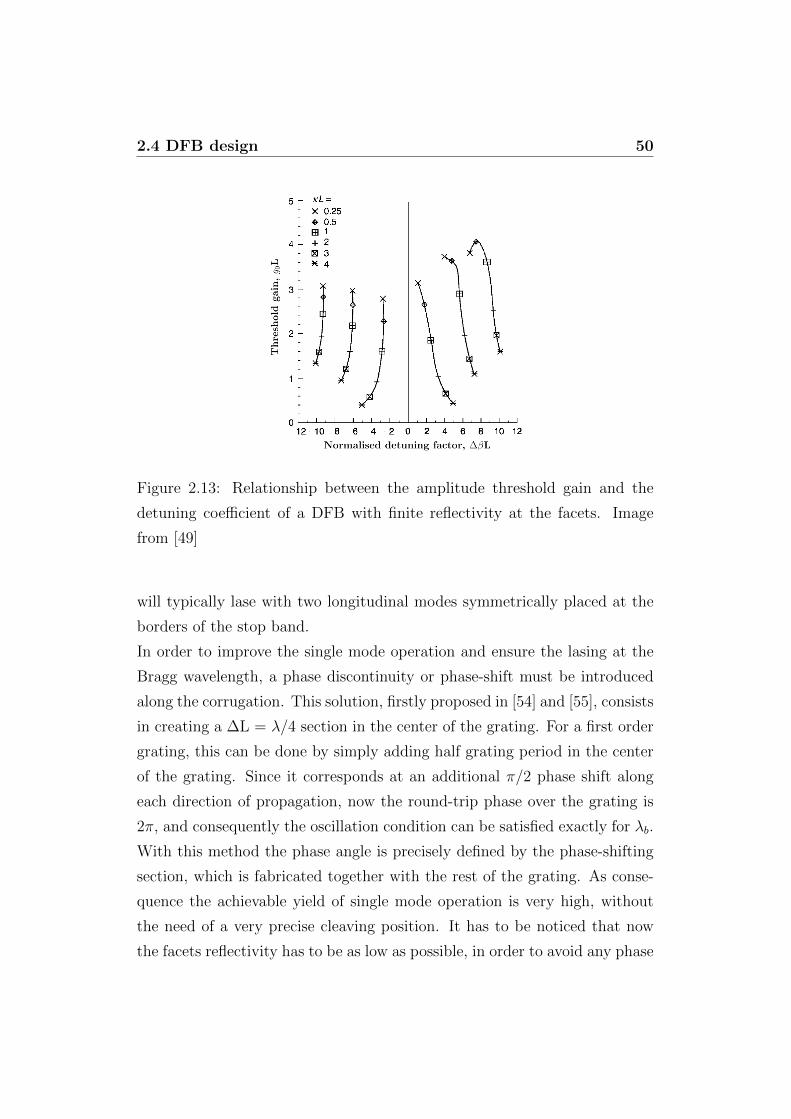
Figure 2.13: Relationship between the amplitude threshold gain and the
detuning coefficient of a DFB with finite reflectivity at the facets. Image
from [49]
will typically lase with two longitudinal modes symmetrically placed at the
borders of the stop band.
In order to improve the single mode operation and ensure the lasing at the
Bragg wavelength, a phase discontinuity or phase-shift must be introduced
along the corrugation. This solution, firstly proposed in [54] and [55], consists
in creating a ∆L = λ/4 section in the center of the grating. For a first order
grating, this can be done by simply adding half grating period in the center
of the grating. Since it corresponds at an additional π/2 phase shift along
each direction of propagation, now the round-trip phase over the grating is
2π, and consequently the oscillation condition can be satisfied exactly for λb.
With this method the phase angle is precisely defined by the phase-shifting
section, which is fabricated together with the rest of the grating. As conse-
quence the achievable yield of single mode operation is very high, without
the need of a very precise cleaving position. It has to be noticed that now
the facets reflectivity has to be as low as possible, in order to avoid any phase

2.4 DFB design 51
interferences caused by backreflections at the facets. In [56] it is suggested
that the residual facet reflectivity should be lower than 1% in order to get a
high single mode yield.
The structure is conveniently modelled using the matrix formalism, consid-
ering two L/2 long gratings separated by the λ/4 section. The oscillation
condition follows [48]:
γLcoth
(γL
2
)+ j(∆βL+ jg0L) = ±κL (2.21)
Figure 2.14 shows the numerical solutions for the oscillation condition. The
graph shows the solutions compared to the uniform grating case, for a 500
µm long grating with κ = 40 cm−1 (κL = 2). It is clear that the phase
Figure 2.14: Allowed resonance modes for DFB lasers with different grating
structures: a) Uniform grating; b) λ/4 shifted grating. Image from [49]
degeneracy has been removed by the λ/4 shifting section, since the mode
with the lowest threshold gain is now placed exactly at the Bragg wavelength.
Moreover, only one mode is allowed at the lowest threshold gain, ensuring
single mode operation. Finally, the large difference in threshold gain between

2.4 DFB design 52
the fundamental mode and the ± 1 modes turns into a high SMSR also when
the laser is pumped at high power.
The effect of the phase shifting section can be also observed on the reflectivity
spectrum of the grating, which modifies by creating a deep notch in the center
of the stop band (Figure 2.15).
Figure 2.15: Spectrum reflectivity of a) uniform grating and b) λ/4 phase
shifted grating.
The phase-shifted gratings were chosen to be used in the devices for the
mm-wave generation, thanks to their single mode operation at the designable
Bragg wavelength.
2.4.4 Side-etched gratings for post-growth fabrication
As previously described, Bragg gratings are formed by producing a peri-
odic modulation of the refractive index seen by the propagating mode. In
DFB lasers, the conventional way to define gratings relies on the etch of the
material on the top of the active region, followed by a subsequent material
regrowth. However, the regrowth over a grating structure greatly compli-
cates the epitaxial growth process and increases fabrication time and cost.
Moreover, the devices for the mm-wave generation require the integration of
other optical structure such as couplers, tapers and attenuators, which fur-
ther increases the fabrication challenges. In order to remove the necessity of
a regrowth fabrication process, laterally-coupled Bragg gratings can be used.

2.4 DFB design 53
Figure 2.16: Lateral coupled grating.
As shown in Figure 2.16, a grating can be fabricated by laterally etching
the active waveguide. This structure, firstly proposed in [57], combines the
lateral optical confinement of the ridge waveguide with distributed feedback
from gratings etched along the side of the waveguide. A laterally-coupled
grating is simply formed by a waveguide of width W, where lateral recesses
of depth d and period Λ0 create the rectangular refractive index profile previ-
ously described. The periodic lateral corrugation of the waveguide interacts
with the evanescent tails of the propagating waves, producing a reflection of
the field that satisfy the Bragg condition. This approach offers a very high
flexibility in designing the coupling coefficient κ, since its value can be de-
fined by either varying the recess depth d or the waveguide width W : higher
values of the ratio W/d lead to lower values of κ, and vice versa.
This type of grating can be fabricated using a fully post-growth technology,
allowing an easier integration with the other optical structures. The gratings
are defined together with the rest of the device in a single lithographic step,
with a mask defined by Electron Beam Lithography. This technology allows
a superb control on the geometrical dimension of the structures, which turns
into a very precise definition of their optical characteristics.
Laterally-coupled gratings allow a very high flexibility also in the design of
their Bragg wavelength. From the Bragg condition λb = 2neffΛ0, it turns
out that both the effective refractive index neff and grating period Λ0 can

2.4 DFB design 54
be changed.
By varying the grating period Λ0, only a discrete tuning of the Bragg wave-
length is achievable. The typical resolution of the electron beam lithography
tools does not allow a wavelength tuning resolution better than around 3
nm, since a small variation of the grating period leads to a big change in λb.
The range of tuning is very wide, and it is only limited by the material gain
band.
On the other hand, a fine quasi-continuous tuning can be obtained by chang-
ing neff , through the variation of waveguide width W or recess depth d.
A small variation of W or d corresponds to a small variation of λb, and
therefore, under normal fabrication tolerances, a spacing resolution of 100
pm (12.5 GHz) is achievable. However, the maximum allowed variation of
W and d limits the tuning bandwidth to a few nanometres. The waveguide
width W is limited by the fact that the grating has to sustain only the fun-
damental mode; the recess depth d is limited by the RIE-lag, a fabrication
issue that will be widely discussed in Chapter 3.
The optimal solution is the combination of the variation of the two effects.
It can be obtained by jointly modifying both the grating period Λ0 and the
refractive index neff , thus achieving a fine tuning of λb over a wide range of
wavelengths (Figure 2.17).
Figure 2.17: Wide quasi-continuous tuning bandwidth achievable using lat-
eral coupled gratings.
The devices for the mm-wave generation required only a small variation
of Bragg wavelength between the different DFBs within the same chip. Since

2.4 DFB design 55
the frequency range of interest for the generated mm-wave signals was up to
40 GHz, a Bragg wavelength spacing of 20 GHz was designed. It was achieved
by changing only the waveguide width, by steps of 25 nm from 2.375 µm to
2.425 µm, while all the DFBs had a period Λ0 of 242 nm and recess depth d
of 400 nm.
However, further studies on the wide quasi-continuous tunability were car-
ried out, in order to use this technology to fabricated multi-wavelength laser
arrays suitable for Dense Wavelength Division Multiplexing (DWDM) ap-
plications. The post-growth fabrication ensures low production costs and
allows for a further monolithic integration with other optoelectronic devices
on the same chip. It was found that it is possible to obtain a notable wave-
length tunability for a single grating period while maintaining an optimal κL
product. By choosing the right values of waveguide width and recess depth,
the coupling coefficient κ can be kept close to the one that ensures the best
performances in terms of threshold current and SMSR [58, 59].
In order to tune the Bragg wavelength, action on the variation of the waveg-
uide width W is more advisable rather than changing the recess depth d.
This approach allows to obtain more constant κ values over a wide Bragg
wavelength range. It avoids fabrication problems that could affect the fine
control of the lateral etch depth between the grating teeth (intended as the
space between the laterally not etched parts of the grating), with a subse-
quent modification of the expected wavelength spacing. Figure 2.18 shows
the Bragg wavelength as a function of the waveguide width W, for different
recess depths d; the gray bands on the background represent different ranges
of the product κL.
In the given range of waveguide width W, a high value of recess depth
(i.e. d = 0.5 µm) ensures a wide range of wavelength tunability, at the
expense of a large variation in the κL. On the other hand, a low value of d
(i.e. d = 0.1 µm) allows an almost constant κL product, but it only allows
for a limited tuning of the Bragg wavelength. A trade-off can be found by

2.5 Couplers 56
Figure 2.18: Bragg wavelength as a function of the waveguide width W,
for different recess depths d; the gray bands on the background represent
different ranges of the coupling coefficient κL.
fabricating gratings with a recess depth of 0.3 µm: a range of wavelength
tunability of 3.5 nm is achievable, while keeping 2≤ κL ≤4. As it will be
discussed in Chapter 4, such a κL range ensures values of SMSR larger than
40 dB, since it avoids spatial hole burning effects that could perturb the
single longitudinal mode operation. The promising approach outlined here
is demonstrated to be capable of producing a DFB laser array with a quasi-
continuous tunability over a wide range of wavelength, always ensuring high
values of SMSR. Moreover, thanks to the post-growth fabrication process,
the fine frequency spacing can be precisely fixed by manufacture, without
a critical adjustment of operating conditions of the laser such as injected
current or temperature.
2.5 Couplers
The mutual injection in the devices Design 1 and Design 2 (Figure 2.1)
is achieved through optical couplers. As it has been discussed in Section 2,
the devices differed in the type of optical coupler used. In order to achieve a
2.5 Couplers 57
low coupling factor, an evanescent field coupler was used in the Design 1. A
Multi Mode Interference (MMI) coupler was used in the Design 2, in order
to couple 50% of the optical power while keeping down the coupler size. This
section details the design of the couplers, also analysing their fabrication
tolerances.
2.5.1 Evanescent field coupler
Evanescent field couplers, also called directional couplers, transfer the op-
tical power between two parallel running waveguides through the overlapping
tails of their evanescent fields. In case of identical waveguides, the propaga-
tion constants are matched, and the power is periodically transferred from
one waveguide into the other. This transfer can be formulated as [60]:
P1(z) = P1(0)cos2(ηz) (2.22)
P2(z) = P1(0)sin2(ηz) (2.23)
where P1(0) is the input power, P1(z) and P2(z) are the optical powers
travelling respectively in the first and in the second waveguide. η represents
the coupling factor, which strongly depends on the width of the gap g between
the waveguides. It is clear that an evanescent coupler is able to transfer any
desired fraction of optical power, just by tuning the length of interaction or
the gap between the waveguides. At the distance z = Lπ all optical power is
coupled into the second waveguide: the parameter Lπ is called beating length,
and it is inversely proportional to the coupling factor η.
The basic idea can be reiterated in order to couple the power travelling in a
waveguide into other two, symmetrically placed beside it. BPM simulations
were performed aiming the definition of the optimal interaction length and
gap width g to achieve 1% of coupling, as required by the design 1.
Figure 2.19a shows how the optical power is exchanged between the
waveguides along the propagation. At the beginning the central waveguide

2.5 Couplers 58
Figure 2.19: a) BPM simulations of three parallel identical waveguides, gap
width g = 1 µm. b) Contour map of the propagating optical fields after
different length z of propagation.
carriers all the optical power. During the propagation it is coupled into the
lateral waveguides, till when at Lπ = 680 µm it is fully and equally trans-
ferred into them. Then, as the propagation continues, the optical power
is transferred back into the central waveguide, following the periodical be-
haviour predicted by the theory. Figure 2.19b shows the cross section of the
waveguides after different length z of propagation: the contour map of the
propagating fields tells how the propagating mode is split between the three
waveguides.
From Equation 2.23, the amount of transferred power does not depends only
on the length of interaction, but also on the coupling factor η. Since it
strongly depends on the gap width g, simulation were performed also for
different values of g (Figure 2.20).
The simulations were carried out for the already discussed standard 2 µm

2.5 Couplers 59
Figure 2.20: Coupled power into one of the lateral waveguides as a function
of the coupler length, for different gap width g.
width waveguides, and the distance between them was varied between 500
nm to 1250 nm. As expected, the power is more effectively coupled when
the waveguides are closer. For g = 500 nm, Lπ is only 230 µm, while as the
gap increases the power is fully transferred after several hundreds of microns.
Despite the coupling factor required (1%) is low and can be achieved through
short interaction lengths, in order to reduce the size of the coupler one would
choose the smallest gap possible. However, fabrication tolerances have to be
kept into account, since a non-optimal etch can strongly affect the coupling
factor. Figure 2.21 shows how the etch depth can affect the coupled power.
The simulation refers to a coupler 50 µm long, for different gap widths. The
coupled power is shown as a function of the etch distance from the core’s top
edge: negative values represent an over-etch of the material, while positive
values represent an under-etch.
It is clear that evanescent couplers are very sensitive to fabrication tol-
erances: a depth inaccuracy of few tens of nm can cause huge changes in
the coupled power. An over etch may lead to a total absence of coupling,
while an under etch may several increase the coupled power. The effects of

2.5 Couplers 60
Figure 2.21: Coupled power as a function of the etch distance from the core’s
top edge. The simulation refers to a coupler 50 µm long, for different gap
widths.
an inaccuracy in the etch depth are stronger in case of under etch and small
gaps g. Moreover, the technology used to fabricate the devices (Chapter 3,
Section 3.5.2) makes an under etch more likely to happen than an over etch,
especially for small values of g. For these reasons a trade off between the
coupler compactness and fabrication tolerances had to be found. In order to
couple 1% of power a gap width g of 1 µm was chosen: it ensured acceptable
fabrication tolerances while keeping down the total length of the coupler; the
interaction length required was 50 µm.
2.5.2 MMI
The Design 2 requires a coupling factor of 50% between the lasers, which
means all the output power of the DFB-3 is split between DFB-1 and DFB-
2. Such high value of coupling makes the use of an evanescent coupler un-
favourable. As shown in Figure 2.20, in order to split the input power into
the lateral waveguides a coupler 700 µm long would be needed5. Different
5Using a gap width g of 1000 nm for a reliable fabrication.

2.5 Couplers 61
structures can be used to couple high levels of optical power, while keeping
the coupler compact. The most common geometries are Y-junction couplers
[61] and MultiMode Intereference (MMI) couplers [62]. Both of them ensure
a low device size but also create intra-cavity back reflections, which are un-
desired here. However, since these back reflections can be minimised in a
MMI coupler, this structure was preferred.
The theory behind MMI couplers operation and properties is well under-
stood and numerous papers have been published, dealing with their design
and fabrication issues. MMI couplers are based on the self-imaging nature
of multimode waveguides. Self-imaging is a property by which an input field
profile is reproduced in single or multiple image at periodic intervals along
the propagation direction of the guide [63]. Depending on the application,
MMI couplers can be designed to have several input and output waveguides;
a simple and effective design outline can be found in [64] for NxN, 1xN and
2xN couplers, and alternatively in [65] for 1xN couplers. Figure 2.22 shows
an 1xN coupler, used in the design 2 (N = 2) and design 4 (N = 3).
Figure 2.22: 1xN MultiMode Interference coupler. The wide central area
represents the multimode waveguide where the interference occurs. The input
waveguide is placed at W/2, while the output waveguides are equally spaced
of W/N.
The central waveguide is designed to support several lateral modes, typ-
ically more than three. Depending on the ratio L/(W )2 and on the lateral

2.5 Couplers 62
positions of the input and output waveguides, different self-imaging arrange-
ments can be obtained [66]. As the self-imaging depends on the interference
between the different modes, the coupling length Lc between the first two
lowest order modes can be used as a characteristic dimension:
Lc ≡4neffW
2eq
3λ(2.24)
where neff and Weq are respectively the effective refractive index and
the equivalent width if the waveguide. Weq takes into account the lateral
penetration depth of each mode’s field, considerable in case of low contrast
waveguides, and can be calculated as [62]:
Weq ' W +
(λ
π
)(n2eff − n2
c
)(−1/2)(2.25)
where nc is the effective refractive index of the cladding. It is clear as
for strongly guiding structures Weq ' W . If the input waveguide is placed
in the center of the multimode waveguide (Figure 2.22), the self-imaging is
obtained by linear combination of the symmetric modes. The self-images
appears at distances
L =M
N· 3Lca
(2.26)
where N is the number of images. M is an integer without common
divisors with N, that define the different distances where the N self-images
appear. The integer parameter a characterise the type of MMI coupler [64]:
in case of 1xN coupler a = 4, and output waveguides have to be symmetrically
located with equal spaces of W/N (Figure 2.22).
L represents the length of the multimode waveguide; it indirectly depends on
the square of the waveguide width W. In order to keep the coupler compact,
W has to be chosen the smallest possible. However, two conditions have to
be satisfied: the multimode waveguide has to be able to sustain at least N+1
lateral mode, in order to obtain a low-loss and well-balanced splitting of the
input field, and has to allow an adequate output waveguides separation, to
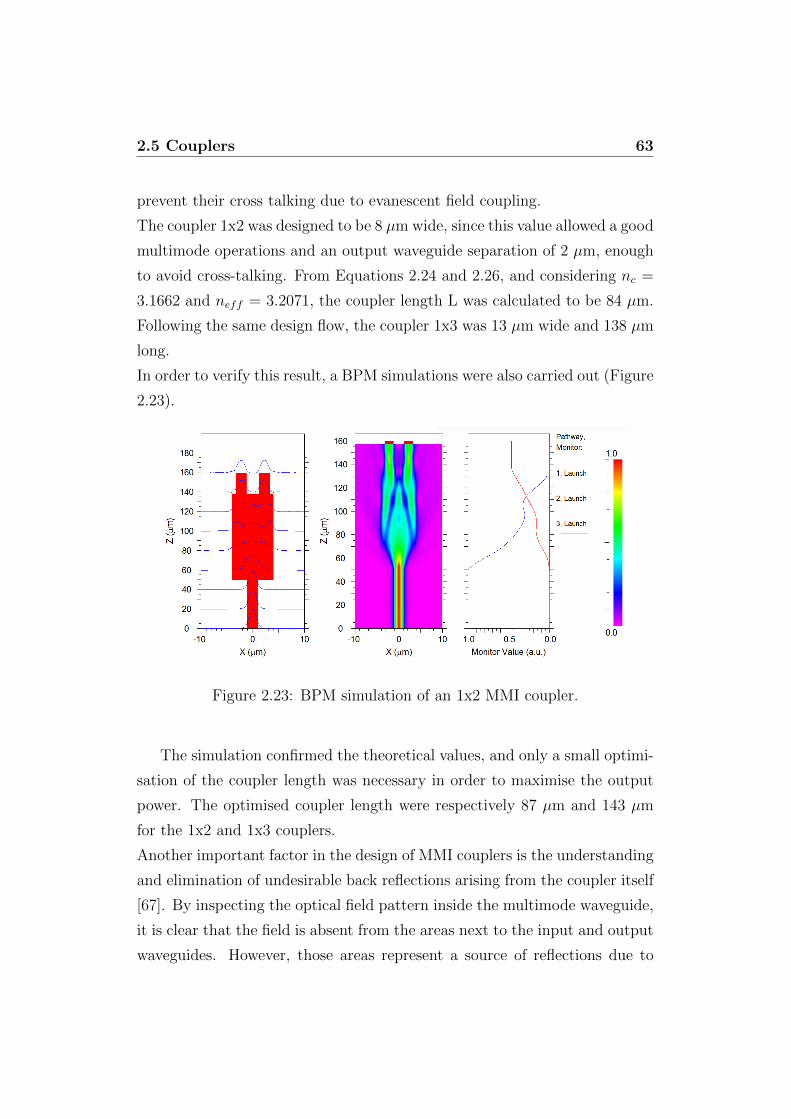
2.5 Couplers 63
prevent their cross talking due to evanescent field coupling.
The coupler 1x2 was designed to be 8 µm wide, since this value allowed a good
multimode operations and an output waveguide separation of 2 µm, enough
to avoid cross-talking. From Equations 2.24 and 2.26, and considering nc =
3.1662 and neff = 3.2071, the coupler length L was calculated to be 84 µm.
Following the same design flow, the coupler 1x3 was 13 µm wide and 138 µm
long.
In order to verify this result, a BPM simulations were also carried out (Figure
2.23).
Figure 2.23: BPM simulation of an 1x2 MMI coupler.
The simulation confirmed the theoretical values, and only a small optimi-
sation of the coupler length was necessary in order to maximise the output
power. The optimised coupler length were respectively 87 µm and 143 µm
for the 1x2 and 1x3 couplers.
Another important factor in the design of MMI couplers is the understanding
and elimination of undesirable back reflections arising from the coupler itself
[67]. By inspecting the optical field pattern inside the multimode waveguide,
it is clear that the field is absent from the areas next to the input and output
waveguides. However, those areas represent a source of reflections due to

2.5 Couplers 64
the step-like refractive index transition. It has been demonstrated that by
bevelling off all of the right-angled edges of the coupler corners, the return
loss can be reduced up to -30 dB [68].
Figure 2.24: Schematic of a 1x2 MMI coupler optimised for low back reflec-
tions.
Following this approach, the input/output waveguides were tapered by
an angle θ = 20 , as shown in Figure 2.24. The angle θ was chosen to be
twice as large as compared to the divergence angle of the light entering in
the MMI section, that was estimated to be 10 from the BPM simulation.
Since the optical fields do not interact immediately with the side-walls of the
MMI coupler, the multimodal interference properties were not affected. BPM
simulations confirmed the optimal physical dimensions previously obtained.
As during the mutual injection the couplers are also used in the reverse
direction as power combiners (DFB-1 and DFB-2 are injected into DFB-3),
a second type of reflection was taken into account. An efficient combining
operation requires input fields with equal phase and amplitude. If the two
inputs are 180 out of phase, in the output waveguide the optical power is
minimum since it is mostly reflected back, creating a perfect imaging of the
input guides back to themself. To solve this issues the SOA/attenuators
were placed next to the input/output waveguides: they acted also as phase
adjusting sections, allowing for the optimisation of the input signals.
The effect of fabrication tolerances was investigated in order to address their
effect on the device performances. BPM simulations were carried out, by
varying the calculated optimal physical dimensions. The couplers exhibited
a very good immunity to fabrication tolerances: this characteristic is due
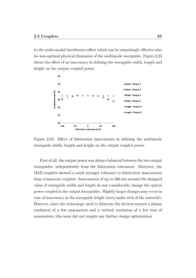
2.5 Couplers 65
to the multi-modal interference effect which can be surprisingly effective also
for non-optimal physical dimension of the multimode waveguide. Figure 2.25
shows the effect of an inaccuracy in defining the waveguide width, length and
height on the output coupled power.
Figure 2.25: Effect of fabrication inaccuracies in defining the multimode
waveguide width, length and height on the output coupled power.
First of all, the output power was always balanced between the two output
waveguides, independently from the fabrication tolerances. Moreover, the
MMI couplers showed a much stronger tolerance to fabrication inaccuracies
than evanescent couplers. Inaccuracies of up to 200 nm around the designed
value of waveguide width and length do not considerably change the optical
power coupled in the output waveguides. Slightly larger changes may occur in
case of inaccuracy in the waveguide height (over/under etch of the material).
However, since the technology used to fabricate the devices ensures a planar
resolution of a few nanometers and a vertical resolution of a few tens of
nanometers, this issue did not require any further design optimisation.

2.6 Design summary 66
2.6 Design summary
For a clear overview of the devices, in the following tables the geometrical
characteristics of the previously described optical structures are reported.
The designed height of all the structures is 1920 nm.
Table 2.1: Waveguide and tapers
Structure Width [µm] Length [µm] Bend radius [µm] Tilting []
Waveguides 2 - 300 -
Spot size converter 2 to 12 100 - 10
Inverse taper 2 to 0 100 - 10
Table 2.2: Gratings
Structure Width [µm] Recess [µm] Length [µm] Period [nm]
DFB-1 2.375 0.4 400 242
DFB-2 2.4 0.4 400 242
DFB-3 2.425 0.4 400 242
Table 2.3: Couplers
Structure Length [µm] Width [µm] gap [µm]
Evanescent 50 2 1
MMI - 1x2 87 In/Out: 2; MM:8 -
MMI - 1x3 143 In/Out: 2; MM:13 -

Chapter 3
Fabrication
The fabrication of the devices required the state-of-the-art techniques for
the manufacture of optoelectronic devices on III-V material, which were not
available at the University of Pavia. For this reason, a visiting research period
at the University of Glasgow (U.K.) allowed for the design and fabrication
of the devices in the newly built James Watt Nanofabrication Centre1.
The centre, one of the most advanced in the U.K. and member of EPSRC Na-
tional Centre for III-V Technologies2, offered the necessary state-of-the-art
facilities, like an Ultra-High resolution Electron beam lithography tool, dry
etching and metal evaporation tools and high resolution scanning electron
microscopes (SEM).
In the following sections, the whole fabrication process is presented, focus-
ing on its most critical steps. First of all, the mask realisation issues will
be briefly described, followed by the detailed description of fabrication tech-
niques used in this work. Special attention will be given to the electron
beam lithography and Reactive Ion Etching issues, such as the RIE lag ef-
fect. Isolation and quasi-planarisation, contact windows opening and final
metallisation processes will also be also described in details.
1www.jwnc.gla.ac.uk2www.epsrciii-vcentre.com/Home.aspx

3.1 Mask realisation 68
3.1 Mask realisation
The very first step of the fabrication process was the design of the lithog-
raphy masks, which contain all the different patterns to be transferred onto
the material by the electron beam lithography tool. The masks were drawn
using the commercial software Tanner L-Edit, which allows a multi-layer and
cell structured design. A multi-layer mask was necessary, since several subse-
quent steps of lithography patterning were used to fabricate the devices; the
cell-structured software allowed a simpler and more flexible design in case of
repeated basic building blocks in the different devices.
During the mask design, all the subsequent fabrication steps had to be kept
in mind, in order to be able to compensate for some of the technology limits
with a smarter design. As shown in the Section 3.5.2, a typical example
comes from the fabrication of gratings and evanescent couplers, where the
RIE lag effect plays an important role. Finally, other smaller layout solu-
tions were devised to ease the characterisation of the devices, such as output
waveguides orientation, contact pads size, etc.
Figure 3.1 shows a complete lithography mask: the devices lie in the central
zone and are organised in six bars, which will be cleaved and mounted on
separate supports.
3.2 Electron Beam Lithography
The fabrication process used to fabricate the devices required several
lithography steps, which were carried out using the High Resolution Elec-
tron Beam Lithography (EBL) tool available in the JWNC. This kind of
tool works in a different way compared to the usual photolithography tools
of the CMOS industry, where the whole pattern is written on the material
with a single exposition using a pre-formed lithography mask. Although also
this approach has the capability to produce micro- and nano- sized patterns,
the need of a pre-formed mask sensibly reduces the flexibility of the process,
since a specific mask has to be produced for each pattern. This fact makes

3.2 Electron Beam Lithography 69
Figure 3.1: Example of a full lithography mask.
the high resolution photolithography sustainable only when used for mass-
production.
For both high levels of resolution and pattern flexibility, required for device
research and prototyping, Electron Beam Lithography (EBL) is the best al-
ternative. EBL is currently the main form of non-optical lithography used
for research regarding nanotechnology applications. The EBL tool used in
this work is a state of the art Vistec VB6-UHR-EWF 100 keV machine, ca-

3.3 Process overview 70
pable of producing a minimum spot size of 4 nm with a step resolution of 0.5
nm, on a writeable field size of 1.3 mm2. The electron beam is steered via
electro-magnets, which are computer controlled.
Figure 3.2: Basic steps to transfer a computer-generated pattern onto the
sample
Figure 3.2 shows how the mask is directly formed on the sample: a highly
focused electron beam writes the masking pattern on the sample surface,
which was pre-coated with an electron sensitive resist. The sample is then
dipped into a specific developer, which removes the exposed or unexposed
areas depending on the tone of the resist (Figure 3.2).
In a positive tone resist, the areas exposed to the electron beam become
soluble to the specific resist developer, while the unexposed area remains in-
soluble. A negative tone resist works contrariwise: the exposed areas becomes
insoluble to the resist developer. The resist used in this work are the Poly-
Methyl MethAcrylate (PMMA, positive tone) and the Hydrogen SilsesQuiox-
ane (HSQ, negative tone): both of them were deposited by spinning and
ensured a very high patterning resolution.
3.3 Process overview
The full fabrication process is formed by more than 50 steps, that can be
grouped in 6 main steps:
• Sample preparation and markers definition

3.4 Sample preparation 71
• Waveguides definition
• Waveguides isolation and quasi-planarization
• Contact windows opening
• Metal depositions
• Cleaving and mounting
This process flow applies to most of the lasers fabricated in the JWNC,
regardless the material and the cavity geometries. However, details as etching
recipes, electron beam doses and layer thicknesses are specific to the type
of material, device or geometry to be fabricated. In the following sections
the most critical steps are described, focusing on the crucial aspects which
allowed a successful fabrication.
3.4 Sample preparation
The material described in Section 2.2 comes in a 2 inches wafer. Given the
high price of a single wafer (1250£) and the research nature of this project,
only few devices were fabricated during each run of fabrication. This re-
quired the use of small portions of the original wafer; Figure 3.3 shows how
the material was firstly cleaved in four pieces and subsequently divided in
small rectangular samples; the remaining parts were used for etch tests.
The wafer was cleaved using a diamond tip: a few millimetres scratch par-
allel to one of the crystallographic axis is enough to cause a fracture along
the material. The precision of this step was crucial to obtain well aligned
devices when finally cleaved and divided in different bars.
Once the small rectangular samples were obtained, the very first step of
the fabrication process was cleaning. To remove all the organic and inor-
ganic contaminants, the sample was dipped into Opticlear, then in Acetone
(CH3COCH3) and finally in Isopropyl Alcohol (IPA, C3H8O), five minutes

3.4 Sample preparation 72
Figure 3.3: Cleaving procedure to divide the original wafer in small rectan-
gular pieces
for each solvent. The cleaning was performed in an ultrasonic bath, to en-
hance the cleansing effect. For the final rinse IPA was used instead of water,
since IPA leaves less residual than water when dried using a nitrogen blow.
This solvent based cleaning was followed by an oxygen ashing, in order to
physically remove any contaminant left. Since the sample must preserve high
levels of cleanliness during the whole fabrication process, this basic cleaning
procedure (except the Opticlear, used only in case of organic contaminants)
was repeated before and after every fabrication step. Finally, the ultrasonic
bath was no longer used after the waveguides definition, to avoid any me-
chanical stress that could break the etched structures.
3.4.1 Markers definition and lift-off technique
Any type of multiple-stage lithography requires the definition of align-
ment markers. It is particularly important in case of EBL, since the align-
ment process is automated and requires well defined and contrasted markers:
in this work metallised markers were used, but other techniques were avail-
able, such as etched markers.
The metallised markers are small gold-covered squares, usually 40x40 µm
big and 500 µm spaced, placed as a frame all around the central area where
the devices pattern will lie. Each lithography step will refer to these small

3.4 Sample preparation 73
squares, ensuring the correct alignment of the different patterns; before each
EBL writing, an accurate inspection checked the good state of the markers,
to avoid that any imperfection of their edges could spoil the correct align-
ment.
Figure 3.4: Lift-off technique (not to scale) a) Resist profile after EBL and
development b) Metal deposition c) Lift-off in hot acetone d) Gold pattern
transferred
The markers were fabricated using the lift-off technique (Figure 3.4): this
method was used twice during the whole fabrication process, every time a
precise and confined area of the sample had to be covered by a metal layer.
Firstly, a double layer of PMMA (positive tone resist) was spun on the sam-
ple: the first layer was 1.2 µm thick, while the second layer was only 110
nm thick. This double layer ensures a better uniformity of the resist over

3.5 Waveguides definition 74
the sample and creates an undercut profile of the resist once exposed and
developed. This undercut profile was formed by choosing a PMMA with a
lower sensitivity as top layer. As the latter layer is less sensitive to the elec-
tron beam, it resulted to be harder to be removed by the developer, creating
the shelf-like profile shown in Figure 3.4a. The ledges prevented the resist
sidewalls from being coated during the subsequent highly-directional metal
deposition (Figure 3.4b). The PMMA was then used as sacrificial layer, as
shown in Figure 3.4c. By dipping the sample in hot acetone, the PMMA
and the overlying metal layer were removed, leaving the metal only where
originally designed (Figure 3.4d).
In summary, the steps so far described were necessary to prepare the sam-
ple for the subsequent process. The sample cleanliness is crucial during the
whole fabrication. The markers were defined to guarantee the correct align-
ment between the subsequent lithography steps; the gold coating ensures a
high contrast to the EBL tool, which can detect them with high precision.
3.5 Waveguides definition
Waveguides definition includes the set of fabrication steps that go from
the pattern writing to the etching of the material, aiming the definition of
the physical structures that will generate and guide the optical signals. This
set of steps is the most crucial for the final outcome of the devices. Every
imperfection would affect the behaviour of the optical structures, and could
even jeopardise the correct operation of the whole devices. As discussed in
Chapter 2, the design of the optical structures has to take into account the
physical limits of these technological steps, in order to avoid the design of
structures that cannot be fabricated with the available technology.
Different techniques are available to define a lithography mask, which will
be used for the subsequent etch of the material. The standard technique
consists of a silica deposition followed by a lithography step for the mask
3.5 Waveguides definition 75
patterning, using a positive tone resist. The pattern is written by exposing
the resist everywhere except over the desired design. The mask is defined
by etching the underlying silica where it is not protected by the resist. Each
of these steps enhances the mask roughness, which will in turn be directly
transferred to the waveguide sidewalls during the subsequent etching. Since
the minimisation of the waveguide losses and back reflections due to sidewall
scattering requires the patterning of a mask with very low edge roughness, an
alternative technique was used. This method consists of using the negative
tone resist HSQ. This material was initially developed in the microelectronics
industry as a spin-on dielectric, but showed brilliant patterning characteris-
tics. The advantage of using this resist is that, once developed, it actually
forms a SiO2 pattern that can be directly used as hard mask for the subse-
quent etching. Apart from resolution and roughness benefits due to direct
writing of the mask, it also avoids the requirement of an etch mask deposi-
tion, lithography, etch and further resist removal [69]. Major investigation
and development of the HSQ lithography process was conducted at JWNC
by a former PhD student, Gabor Mezosi, resulting in a reliable and stable
technique for use in photonic device fabrication.
The HSQ deposition was performed by spinning, followed by a baking of the
sample at 91.5 C for 15 minutes; this operation was necessary to prepare
the resist for the electron beam lithography, drying the solvents contained
in it. Since the resist sensitivity to the electron beam strongly depends on
the age of the resist, generally it would be advisable to run a writing test
before this step, with the goal of determining the optimal dose of electrons
[µCcm−1] to be used during the pattern writing.
After the lithography step, the resist had to be developed: the sample was
dipped in TetraMethylAmmonium Hydroxide (TMAH) for 30 seconds, at 22.5C, then rinsed in reverse osmosis water (RO water) and IPA to stop the de-
velopment process. To obtain reliable results, temperature and time had to
be kept constant during the developing of the test samples and the ”real”
sample.
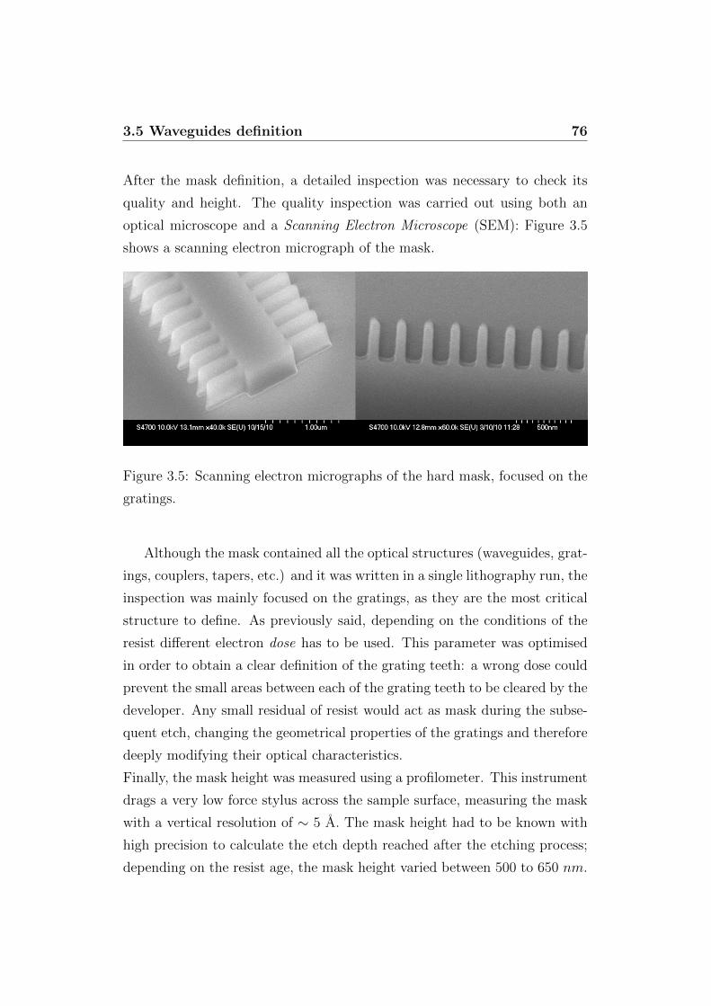
3.5 Waveguides definition 76
After the mask definition, a detailed inspection was necessary to check its
quality and height. The quality inspection was carried out using both an
optical microscope and a Scanning Electron Microscope (SEM): Figure 3.5
shows a scanning electron micrograph of the mask.
Figure 3.5: Scanning electron micrographs of the hard mask, focused on the
gratings.
Although the mask contained all the optical structures (waveguides, grat-
ings, couplers, tapers, etc.) and it was written in a single lithography run, the
inspection was mainly focused on the gratings, as they are the most critical
structure to define. As previously said, depending on the conditions of the
resist different electron dose has to be used. This parameter was optimised
in order to obtain a clear definition of the grating teeth: a wrong dose could
prevent the small areas between each of the grating teeth to be cleared by the
developer. Any small residual of resist would act as mask during the subse-
quent etch, changing the geometrical properties of the gratings and therefore
deeply modifying their optical characteristics.
Finally, the mask height was measured using a profilometer. This instrument
drags a very low force stylus across the sample surface, measuring the mask
with a vertical resolution of ∼ 5 A. The mask height had to be known with
high precision to calculate the etch depth reached after the etching process;
depending on the resist age, the mask height varied between 500 to 650 nm.

3.5 Waveguides definition 77
3.5.1 Reactive Ion Etching
Once the patterning mask was written on the sample, the next fabrication
step was etching the material. Dry and wet etching were available techniques,
but the former was chosen since it holds several advantages. This includes
strong etch anisotropy, less mask undercutting and greater repeatability, al-
lowing the definition of smaller structures. Dry etching techniques are based
on the chemical and physical interactions of a gas in plasma state with the
sample in order to remove the desired material.
The method of dry etching employed in this work is the Reactive Ion Etching
(RIE), using an ElectroTech SRS Plasmafab 340 machine. Typically, a RIE
Figure 3.6: Simplified scheme of a typical Reactive Ion Etching machine (not
to scale)
machine consists of a pressure controlled chamber containing two parallel
electrodes, of which the lower one holds the sample to be etched, as shown
in Figure 3.6. The reactive species are injected in the chamber via a gas
inlet; the plasma is generated using a RF power, typically at 13.56 MHz,
capacitively coupled to the lower electrode, whilst the upper is grounded.
The reactants are therefore transported to the sample surface, where they
are absorbed. The ions chemically react with the materials on the samples
surface, while some atoms are physically knocked off by the ion bombard-
ment: the very anisotropic etch profile is due to the mostly vertical delivery

3.5 Waveguides definition 78
of reactive ions. The etching phase is finally followed by the desorption of
the by-product compounds from the surface, which are pumped away by the
system. Etch conditions in an RIE system depend on many process param-
eters, such as gas flows, RF power, chamber pressure and temperature.
Reactive Ion Etching of InP based materials is a mature research field, since
several chemistries and technologies have been investigated during the past
years. Each of them produces good sidewall verticality, etch rate and mask
selectivity. The more commons are based on Cl2 and CH4/H2 [70–75].
Chlorine based chemistries have a fast etch rate, but require high substrate
temperatures ( > 150 C) to promote the desorption of the non-volatile etch
products (InClx), necessary to maintain a smooth surface after etching. Such
high temperature however does not allow the use of most of the photoresists
as an etch mask.
The chemistry available in the JWNC and thus used in this work is based
on Methane Hydrogen. It was first proposed for InP RIE processing in 1989
[76]: it can be operated at room temperature, provides good anisotropic pro-
files, smooth surfaces and acceptable etch rates of a few tens of nm/min.
An issue with this type of etching is the formation of hydrocarbon polymers
on inert surfaces, that slows down the etch rate and increases the surface
roughness. This hydrocarbon based polymers deposition can be mitigated
by the addiction of oxygen (O2), which removes them by dissociation; more-
over, as reported in [75, 77], it also helps in producing more vertical etched
sidewall. Normally, the addiction of O2 would be a problem when etching
Al-containing compounds: oxygen readily oxidises the aluminium forming
alumina (Al2O3), which is notoriously difficult to etch. However, this turned
to be an advantage here, since the etching had to be stopped at the depth
corresponding to the first aluminium containing layer, i.e. 1920 nm, as shown
in Section 2.2. Figure 3.7 shows a perspective view of a lateral etched grat-
ing, etched with the chemistry CH4/H2/O2.
Using these gases, the average etch rate of the upper cladding (compo-
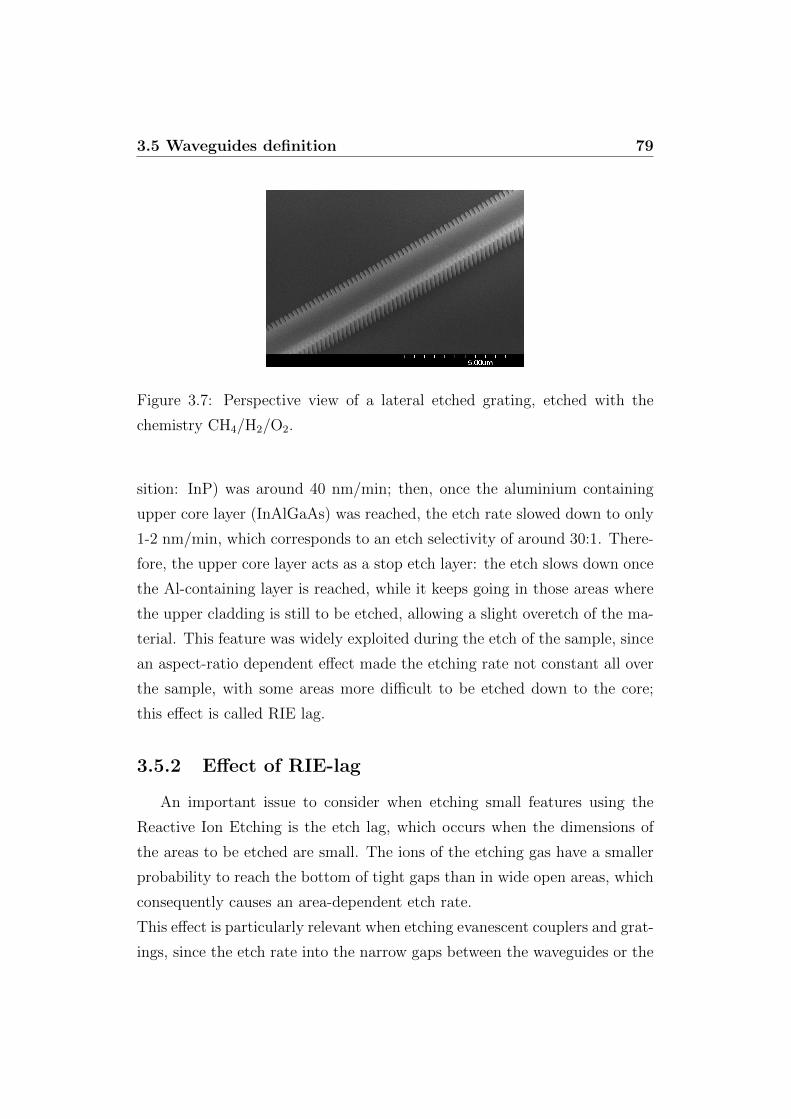
3.5 Waveguides definition 79
Figure 3.7: Perspective view of a lateral etched grating, etched with the
chemistry CH4/H2/O2.
sition: InP) was around 40 nm/min; then, once the aluminium containing
upper core layer (InAlGaAs) was reached, the etch rate slowed down to only
1-2 nm/min, which corresponds to an etch selectivity of around 30:1. There-
fore, the upper core layer acts as a stop etch layer: the etch slows down once
the Al-containing layer is reached, while it keeps going in those areas where
the upper cladding is still to be etched, allowing a slight overetch of the ma-
terial. This feature was widely exploited during the etch of the sample, since
an aspect-ratio dependent effect made the etching rate not constant all over
the sample, with some areas more difficult to be etched down to the core;
this effect is called RIE lag.
3.5.2 Effect of RIE-lag
An important issue to consider when etching small features using the
Reactive Ion Etching is the etch lag, which occurs when the dimensions of
the areas to be etched are small. The ions of the etching gas have a smaller
probability to reach the bottom of tight gaps than in wide open areas, which
consequently causes an area-dependent etch rate.
This effect is particularly relevant when etching evanescent couplers and grat-
ings, since the etch rate into the narrow gaps between the waveguides or the

3.5 Waveguides definition 80
grating teeth can be significantly slower than into the other open areas of
the sample. As shown in Section 2.5, it is crucial to etch down to the first
aluminium containing layer everywhere in order to obtain an experimental
behaviour closer to the simulations. Most of the areas can be cleared thanks
to the stop etch layer, just by etching the material for a slightly longer time.
Nevertheless, since the upper core layer is used as part of the electron con-
finement layers, it would be undesirable to etch through it with a too long
overetch. In fact, it is worth to remember that the etch does not stop, but
just slows down when the Al-containing layer is reached. It is therefore nec-
essary to find a trade-off between design and fabrication limits to avoid the
design of structures with too narrow gaps impossible to be cleared.
Figure 3.8 shows the cross sections of two evanescent couplers with different
distance between the two waveguides: in Figure 3.8a the etch did not cleared
the gap of 0.6 µm between the waveguides, whereas Figure 3.8b shows that
a gap of 1 µm can be easily etched down.
Figure 3.8: Cross sections of evanescent couplers with different distance be-
tween the waveguides: a) 0.6 µm far; b) 1 µm far.
With this technology, the minimum gap that can be cleared is 0.7 µm,
slightly overetching the material but without going through the upper core
layer. Therefore, in order to increase the coupling factor longer couplers have
to be designed; gaps smaller than 0.7 µm would not give a reliable results in

3.5 Waveguides definition 81
terms of coupling factor.
The RIE lag may create even bigger problems during the definition of the
lateral etched gratings. As discussed in the previous Chapter, a small un-
deretch in the recess depth of the grating teeth causes a big change in the
optical characteristics. This is due to the fact the optical mode lives at the
very bottom of the grating, which is also the most difficult area to be etched
down to the core. Figure 3.9 shows the cross sections of two gratings with
different recess depths.
Figure 3.9: Cross sections of lateral etched gratings with different etch depth
d : a) d = 300 nm; b) d = 600 nm.
In Figure 3.9a the etch reached the base of the grating: the sidewalls of
the inner part of the grating show a good verticality till down to the core,
where only a slight vertical underetch occurred. Gratings with this etch pro-
file will exhibit optical characteristics very close to the simulations.
On the other hand, the grating shown in Figure 3.9b presents a strong un-
deretch: the recess d was too deep, and the RIE lag effect did not allow a
complete etch of the material. The etch profile in the bottom part of the
grating is noticeable curved: both a smaller recess depth and a vertical un-
deretch are present. This grating will exhibit optical characteristics very far
from those expected from the design, since the grating strength is now con-
siderably reduced.

3.5 Waveguides definition 82
If the designed recess is too deep, the slight overetch normally allowed by the
stop etch layer may be not enough to clear the grating teeth. For this reason,
the RIE lag effect inside the gratings was further investigated. Gratings with
different recess depths were patterned on a test sample, and then etched for
the maximum time allowed by the stop etch layer. Finally, the test sample
was cleaved to measure the cross section of the gratings. Figure 3.10 shows
the effect of the RIE lag on the etch profile inside the gratings.
Figure 3.10: Measurement of the RIE lag effect on the recess depth and
vertical underetch inside the gratings.
Recess depths and vertical underetch were measured: the dashed line
represents the ideal case, where the measured recess depth inside the grating
matches the recess depth d of the mask. For d smaller than 100 nm, the
mask profile could not be successfully transferred to the material because of
the non ideal sidewall verticality. For mask recesses between 100 nm and 400
nm, the grating teeth were well cleared till the very bottom of the waveguide:
the recess depth was very close to the ideal case, and only a negligible verti-
cal underetch was present. This is the range of values that ensures the most
reliable results in terms of optical characteristic of the grating. For d bigger
than 400 nm, the RIE lag was too strong to be compensated by the slight
overetch allowed by the stop etch layer: the difference between the mask re-
cess and the measured recess at the bottom of the grating was considerable,

3.6 Waveguide isolation and quasi-planarization 83
as well as the vertical underetch inside the grating. The etch profile was the
one already shown in Figure 3.9b. In order to fabricate gratings with reliable
optical characteristics these values of recess depth d have to be avoided.
The RIE lag issue is particularly important to take into account when design-
ing gratings where a high precision wavelength spacing is required. Therefore,
the best way to fine tune the Bragg wavelength of the gratings was changing
the waveguide widths W rather than changing their recess depths d. The
RIE lag would not allow a very precise definition of the etch profile inside
the grating, necessary to ensure a tuning of the Bragg wavelength of a few
GHz. On the other hand, the RIE lag effect is negligible when defining the
external sidewalls of the grating, since the area to be etched is much wider.
After the material etching, accurate inspections of the sample were per-
formed using the SEM and the profilometer. If the upper core layer was
reached everywhere on the sample, the etch was considered satisfying. The
following step was the mask removal, performed by dipping the sample for
30 seconds in HydroFluoric acid (HF), which is a very powerful acid able
to attach and dissolve the HSQ mask. The sample was finally rinsed in RO
water and IPA to remove any residual of HF.
In summary, at this stage of the fabrication process the pattern containing
all the designed optical structures was transferred on the material. A RIE
with a chemistry of CH4/H2/O2 was used, which allowed the definition of
very vertical sidewalls. The RIE lag was mitigated with a slight overetch
of the material, allowed by the aluminium containing stop etch layer, and
avoiding the design of too narrow gaps.
3.6 Waveguide isolation and quasi-planarization
After the definition of the waveguides, the next fabrication steps are in-
tended to create the electrical isolation of the sample surface. This is neces-

3.6 Waveguide isolation and quasi-planarization 84
sary because the electrical current has to be injected only into the top area
of the waveguides. Moreover, some of the defined structures do not require
to be electrically pumped, thus they have to be isolated.
The standard technique used for the electrical isolation is the deposition of a
few hundreds nanometers of silica (SiO2), performed by a Plasma-Enhanced
Chemical Vapour Deposition (PECVD). It allows a simple and effective coat-
ing of the whole sample. However, the technique used for the subsequent
metal deposition required a quasi-planarization of the sample surface, since
it is not able to coat vertical sidewalls.
A first deposition of 200 nm of PECVD silica was followed by a layer of spin-
on dielectric. The HSQ was used as liquid glass : it was easily deposited by
spinning and then baked to form an uniform and smooth silica layer on the
sample surface. Figure 3.11 shows the cross section of a waveguide coated
by 200 nm of PECVD silica and the subsequent layer of baked HSQ, 400 nm
thick. A final layer of 100 nm of PECVD silica was deposited in order to
cover cracks that might occur during the baking process.
Figure 3.11: cross section of a quasi-planirized waveguide coated by 200 nm
of PECVD silica and the subsequent layer of baked HSQ
After this set of fabrication steps, the surface of the sample was electrically
isolated and, thanks to the used layer structure, the waveguides were also
mechanically stronger. The semi-planarization process was crucial to allow
3.7 Contact windows opening 85
a final smooth and continuous metal coverage.
3.7 Contact windows opening
After the isolation and quasi-planarization layer, contact windows had
to be opened at the top of those structures which require a direct electrical
access, such as gratings, SOAs and attenuators. Separate contact windows
were opened for each section of the devices, to allow the injection of different
values of current (or reverse bias) into the various optical structures.
A layer of positive resist (PMMA) was spun, followed by a lithography step
to define the pattern. The alignment was guaranteed by the gold markers: a
sub-micrometer precision was mandatory in order to open the contact win-
dows exactly at the top of the waveguides, avoiding a further current injection
in undesired areas. The contact windows were then opened by etching the
isolation layer: also in this case the RIE was the best etch option thanks to
its high anisotropy. A fluorine based gas mixture (CHF3/Ar) was used, as
ensures an elevate selectivity in etching the silica but not the waveguide’s
cap layer and allows a good etch rate around 30 nm/min.
To make sure silica layer was fully etched where needed, the devices larger
features had to be checked. In fact, due to the quasi-planarization process,
SiO2 is thicker on the top of the wider waveguides, and a correct etch depth
here ensures a successful contact windows opening everywhere. An accu-
rate optical microscope inspection was sufficient to assess to outcome of this
fabrication step. Figure 3.12 shows the optical pictures of an output taper
before and after the window opening: the cap layer is well visible after the
etch, denoting that the correct etch depth was reached. The multicoloured
appearance of the sample is due to the interference of the white light com-
ing from the microscope with the isolation layers, which have a thickness
comparable with the visible light.
The mask was finally stripped off with an oxygen plasma ash, that re-
moved the resist and prepared the sample surface for the subsequent steps.

3.8 Metal depositions 86
Figure 3.12: Optical pictures of an output taper before and after the window
opening: the cap layer is well visible after the etch, denoting that the correct
etch depth was reached
3.8 Metal depositions
Two common techniques for metal deposition are sputtering and evap-
oration. In a sputtering deposition chamber, the sputtered metallic atoms
ballistically fly from the metal target to the sample following random walks.
With this method the metal is deposited as an isotropic film, allowing the
coating of vertical sidewalls. However, this advantage turns in a disadvantage
when a subsequent lift-off process wants to be used to separate the different
contact pads.
In a evaporation chamber, outlined in Figure 3.13, a high energy electron
beam is magnetically focused on a crucible, that contains the metal to be
evaporated.
The metal evaporates because of the high energy of the colliding elec-
trons, producing a diverging cone of atoms which diffuses away from the
source. Thanks to the ultra-high vacuum (10−7 mbar) in the chamber, the
vapour particles travel directly to the sample, where they condense back to
the solid state. This method consents a subsequent use of the lift-off tech-
nique, since it provides a very anisotropic deposition. An uniform metal
layer coats the horizontal surfaces, while only very few atoms deposit on the
3.8 Metal depositions 87
Figure 3.13: Simplified scheme of an electron beam metal evaporator.
vertical and shadowed sidewalls.
Therefore it is also clear why the quasi-planarization of the sample was nec-
essary: the lift-off process requires a very vertical metal deposition, that, on
the other hand, does not allow a nice coating of the waveguide sidewalls.
An appropriate sidewall coating is necessary to delivery the injected current
from the big metal pads to the contact windows at the top of the waveguides:
a thin sidewall metallisation would tend to fuse when a high current density
is applied during the device testing. The planarization solves the problem:
smoothing the waveguide sidewalls, it allows the use of the metal evapora-
tion.
The definition of the pattern for the metallization of the top side of the sam-
ple (p-doped) required a last lithography step: a double layer of PMMA was
spun, and the pattern was written by the EBL tool. After the resist devel-
opment, a strong deoxidant bath in HCl prepared the sample surface for the
p-contact metallisation. A triple layer of titanium (Ti), platinum (Pt) and
gold (Au) was deposited. The Ti was used as an adhesion layer, as it is a re-
active metal that quickly oxidises, adhering well to the underlying silica used
for the isolation layer. However, as its conductivity is not as good as the gold
one, only a thin layer of 30 nm was deposited. A subsequent 60 nm diffusion
barrier layer of platinum was used. A top layer of gold, 340nm thick, was
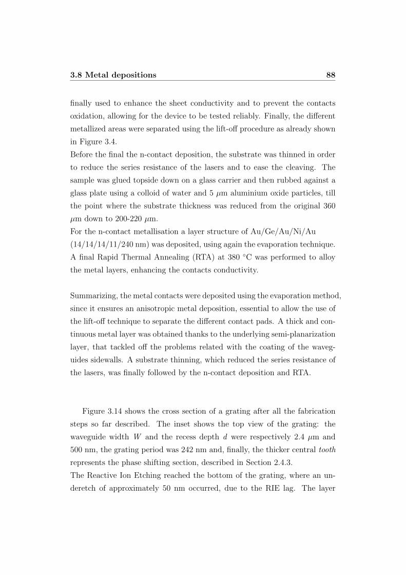
3.8 Metal depositions 88
finally used to enhance the sheet conductivity and to prevent the contacts
oxidation, allowing for the device to be tested reliably. Finally, the different
metallized areas were separated using the lift-off procedure as already shown
in Figure 3.4.
Before the final the n-contact deposition, the substrate was thinned in order
to reduce the series resistance of the lasers and to ease the cleaving. The
sample was glued topside down on a glass carrier and then rubbed against a
glass plate using a colloid of water and 5 µm aluminium oxide particles, till
the point where the substrate thickness was reduced from the original 360
µm down to 200-220 µm.
For the n-contact metallisation a layer structure of Au/Ge/Au/Ni/Au
(14/14/14/11/240 nm) was deposited, using again the evaporation technique.
A final Rapid Thermal Annealing (RTA) at 380 C was performed to alloy
the metal layers, enhancing the contacts conductivity.
Summarizing, the metal contacts were deposited using the evaporation method,
since it ensures an anisotropic metal deposition, essential to allow the use of
the lift-off technique to separate the different contact pads. A thick and con-
tinuous metal layer was obtained thanks to the underlying semi-planarization
layer, that tackled off the problems related with the coating of the waveg-
uides sidewalls. A substrate thinning, which reduced the series resistance of
the lasers, was finally followed by the n-contact deposition and RTA.
Figure 3.14 shows the cross section of a grating after all the fabrication
steps so far described. The inset shows the top view of the grating: the
waveguide width W and the recess depth d were respectively 2.4 µm and
500 nm, the grating period was 242 nm and, finally, the thicker central tooth
represents the phase shifting section, described in Section 2.4.3.
The Reactive Ion Etching reached the bottom of the grating, where an un-
deretch of approximately 50 nm occurred, due to the RIE lag. The layer
3.8 Metal depositions 89
Figure 3.14: Grating cross section taken at the end of the fabrication process.
structure used for the isolation and quasi-planarization layer is well visible
on the sides of the grating: the two layers of PECVD SiO2 (light grey) are
divided by the spin-on glass layer (HSQ, black). The contact window is well
open on the top of the grating, allowing the electrical access to the waveg-
uide’s cap layer. Finally, the metal layer smoothly coated the sample surface
up into the contact window, thanks to the quasi-planarization process. It
is possible to distinguish the first layer of titanium (dark grey), right above
the waveguide’s cap layer and the upper layer of PECVD silica. The thick
top layer is formed by gold, which protects the contacts surface and ensure
a high conductivity.

3.9 Cleaving and mounting 90
3.9 Cleaving and mounting
The very last steps of the fabrication process were intended to separate
the different devices and to mount them onto a suitable support for char-
acterization. The sample was cleaved in different bars, as discussed in the
Section 3.4, to allow the optical access to the output tapered waveguides us-
ing lensed optical fibre. Figure 3.15 shows how the sample looks like after the
whole fabrication process, with the particular of a single cleaved bar. Each
single device presents wide metallized areas, where special designed 10 pins
multiprobes were used to inject different values of current (or reverse bias)
in the different sections of the device.
Figure 3.15: Sample appearance after the fabrication process, with the par-
ticular of a single cleaved bar.
Finally, each bar was mounted on brass submounts using a two compo-
nents conductive epoxy glue. The submount serves as the common ground

3.9 Cleaving and mounting 91
contact for the lasers, for heat dissipation and mechanical support. Figure
3.16 shows a brass submount with two bars of devices, compared with a
common AA battery to better appreciate their size.
Figure 3.16: Devices mounted on a brass submount for characterization

Chapter 4
DFB characterization
The measurements of the devices started from the characterisation of the
DFB lasers, with a complete analysis of their properties. The DFBs represent
the core of the devices, where the optical signals are generated: the correct
operation of the devices depends on their lasing characteristics.
For an exhaustive analysis of the lasers, a large number of gratings, with
different geometrical parameters, was fabricated and characterised.
This chapter gives an overview of the DFBs characterisation: the basics LI
curves (optical output, L, as a function of the injected current, I), wave-
length maps and linewidth measurements are firstly presented, followed by
their stop bands characterisation. The relations between the coupling coeffi-
cient factor of the grating, the threshold current and Side Mode Suppression
Ratio (SMSR) of the lasers are then discussed. The measurements of the
wavelength spacing accuracy are presented and, finally, the chapter closes
with a test of devices lasing stability over the time.
4.1 L-I curves and wavelength maps
The lasers were first evaluated with respect to their basic properties.
Optical power versus injected current measurements were performed on all
the DFBs; a large area photodiode was used to collect the optical power,

4.1 L-I curves and wavelength maps 93
while the temperature of the lasers was kept constant at 20 C, using a
Peltier cell. The SOA/attenuators were biased at transparency.
Figure 4.1: Typical a) L-I curve, b) V-I curve and c) series resistance mea-
sured for the fabricated DFBs.
Figure 4.1a shows a typical L-I curve, measured for one of the fabricated
DFBs. The threshold was reached around 18 mA, which means a threshold
current density of 3.75 kA/cm2, then the output power increased linearly
with the injected current. The maximum injected current was kept below 150
mA: it corresponds to a current density of 30 kA/cm2, which is considered the
upper limit for a safe and reliable operation of these lasers. When the DFBs
were pumped at the maximum current, the emitted optical power collected by
the large area photodiode was up to 3.5 mW; however, an acceptable output
power of 0.5 mW was reached for smaller currents, around three times the
threshold. Figures 4.1b and 4.1c show respectively the curves for the voltage
at the p-n junction and the series resistance of the lasers: the voltage was
limited at 2.4 V for high injected currents, and the measured series resistance
was below 10 Ω. These values were routinely achieved during the different
runs of fabrication, remarking the reliability of the fabrication process.
The optical spectrum of the DFBs was also evaluated. Special lensed optical
fibres were used to collect the light from the output waveguides of the devices.
Figure 4.2 shows that, as expected (Section 2.4), the DFBs with phase shifted
grating lase on a single longitudinal mode at the Bragg wavelength, while the

4.1 L-I curves and wavelength maps 94
uniform gratings lase on two longitudinal modes, placed at the borders of the
stop band.
Figure 4.2: Optical spectrum of phase shifted and uniform gratings, when
pumped at 80 mA.
The λ/4 phase shifting section effectively adjusted the round-trip phase
of the reflected field, allowing the single mode operation: very high values
of Side Mode Suppression Ratio were reported, up to 59 dB in some of the
measured DFBs. Figure 4.3a shows a typical wavelength map of a λ\4 phase
shifted grating, where the optical spectrum is plotted for different values of
current.
Figures 4.3b and 4.3c show respectively the SMSR and the Bragg wave-
length as a function of the injected current, extracted from the wavelength
map. These two curves represent an important result with a view to the
correct operation of the final devices for the mm-wave generation, where
high values of SMSR and tunability are required. The graphs show that an
acceptable SMSR of 40 dB was reached immediately above the threshold;
then, it increased to a stable value of 55 dB, which was maintained up to
very high injected current. At the same time, due to thermal shift, the Bragg
wavelength increased from 1551 to 1554 nm, denoting a wavelength tuning
of 24 pm/mA (3 GHz/mA). With a view to the final devices, these values
suggest that a RF signal could be generated and tuned over a very wide

4.2 Linewidth 95
Figure 4.3: a) Wavelength map of a λ/4 shifted grating; extract data for b)
SMSR and c) Bragg wavelength as a function of the injected current
range of frequencies: ideally it would be possible to obtain up to 360 GHz of
tunability range, just by tuning the DFBs current from 30 to 150 mA.
Higher tunabilities can be achieved by using integrated heaters next to each
DFB [78]. By increasing the temperature of one or more gratings, the las-
ing wavelength can be tuned due to thermal effects. However, in order to
avoid thermal cross talking between the different DFBs, the lasers have to
be placed at larger distances than in the geometries described in Chapter
1, requiring a complete redesign of the devices. Since this aspect was not
considered crucial for the main aim of this work, no further investigations
were carried out.
4.2 Linewidth
The optical linewidth of a laser refers to the optical phase fluctuation of
the lasing longitudinal mode. This is due to two basic phenomena: sponta-
neous emission and carrier density fluctuations [48, 50, 79]. The first one is
present in all lasers: whereas photons generated by stimulated emission are

4.2 Linewidth 96
added in phase to the lasing field, the phase associated with a spontaneous
emitted photon is random. The second phenomenon is inherent only in semi-
conductor lasers, and it results from the proportionality between the carrier
density and the emission frequency of the laser. During a photon emission,
the carrier density changes since an electron decays from conduction band to
valence band. This entails a change in the refractive index and, therefore, in
the instantaneous emission frequency of the laser.
A coherent heterodyne technique [80, 81] was used to measure the linewidth
of the DFBs. Using this method, the optical signal coming from the laser
under test and an optical local oscillator are mixed in a photodiode. The elec-
trical beating of the two signals is downshifted to a lower frequency, equal
to their frequency difference (Figura 4.4a). The output signal of the photo-
diode is measured with an RF spectrum analyzer, which allows an excellent
spectral resolution. The figure 4.4b shows the experimental setup used for
this measurement.
Figure 4.4: a) Coherent heterodyne technique; b) Experimental setup.
Few practical issues had to be considered to perform a correct measure-
ment. This technique requires the use of a local oscillator with a very narrow
linewidth: the downshifted electrical beating is the convolution between the

4.2 Linewidth 97
two original optical signals, and therefore its linewidth is equal to the sum of
the optical signals’s linewidths. A grating-based external-cavity lasers (Agi-
lent 8164A) was used, thanks to its narrow spectral emission (100 kHz) and
its wide continuous tuning range. The coherent detection efficiency was max-
imized using a polarization controller, and an isolator was used to minimize
unwanted back reflections into the DFBs. Finally, the output of the 50/50
coupler was connected to a high speed photodiode (New Focus, bandwidth of
45 GHz), followed by the RF spectrum analyser (Rohde & Schwarz FSV40).
The spectral width of the lasing mode was measured at -20 dB and -30 dB,
then the linewidth at -3 dB was calculate using a Lorentzian fitting. This
was necessary in order to increase the measurement accuracy, minimising the
effects of frequency drifts of DFBs and local oscillator. Figure 4.5a shows a
typical linewidth measurement.
Figure 4.5: a) Typical linewidth measurement; b) DFB linewidth as a func-
tion of the injected current (Ith = 21 mA).
The linewidth of the fabricated DFBs was found to be around 13 MHz,
with a dependence on the current injected into the DFBs (Figure 4.5b).
As predicted by the theory [79, 82], for low levels of injected current (and
therefore output power P) the linewidth was larger, around few tens of MHz.
Then, for higher injected current, the linewidth decreased proportionally to

4.3 Coupling coefficient and stop-band measurements 98
1/P, reaching a minimum value of 10.3 MHz.
The measured values were consistent for all the different DFB lasers that were
characterised, showing a very good uniformity of the lasing characteristics
between the lasers.
4.3 Coupling coefficient and stop-band mea-
surements
When characterizing DFB lasers, another very important parameter to
be measured is the coupling coefficient factor κ of the grating. As discussed
in Section 2.4, a lot of crucial parameters depend on κ, such as grating re-
flectivity and stop band. Moreover, as will be described in the next pages,
the coupling coefficient affects the threshold current and the side mode sup-
pression ratio too. In order to address how this parameter affects the lasing
properties, the coupling coefficient was measured for a large number of DFBs.
Phase shifted and uniform gratings were fabricated on a single chip, using the
technology described in Chapter 3. Waveguide width W and recess depth d
were varied, respectively between 2 and 2.6 µm and between 0.3 and 0.6 µm.
To reduce the degrees of freedom of the problem, all the lasers were 400 µm
long.
As already shown in Figure 4.2, DFBs with uniform grating lase on a bi-
modal regime, with the two modes placed at the borders of the stop band:
this feature was exploited in order to directly measure the stop band width
of the gratings. From the coupled mode theory [48], the grating stop band
measurement allows the calculation of κ as
κ = π · neff ·∆λ
λ2b
(4.1)
where ∆λ is the measured stop band width, neff is the effective refractive
index seen by the propagating mode and λb is the Bragg wavelength of the
grating.

4.3 Coupling coefficient and stop-band measurements 99
The bimodal regime occurs only when the degeneracy of the phase conditions
at the facets are preserved, which means that every reflection from the ex-
ternal ends of the gratings has to be avoided. To do so, long tapers smoothly
connected the gratings to the standard 2 µm waveguides, while the output
waveguides were 10 tilted in order to minimise the backreflections from the
cleaved facets. Moreover, only one side of the gratings was used to collect the
optical signals, while the other one was ended on a inverse tapered waveguide
to ensures even lower backreflections.
The stop band was measured for all the fabricated DFBs, and the coupling
coefficient κ was calculated using the (4.1). Figure 4.6 shows κ as a function
of the grating width, for gratings with different recess depths.
Figure 4.6: Grating coupling coefficient κ as a function of the grating width,
for gratings with different recess depths. Recess depths are expressed in µm.
As expected, κ is decreasing for wider waveguide widths: the mode is
seeing a stronger grating when the waveguide width is small and the recess
depth is big. By increasing the waveguide width on equal recess depth, κ is
decreasing, which means the mode sees a weaker grating. Same effect can be
obtained by decreasing the recess depth on equal waveguide widths; however,
as shown in Figure 4.6, in this case the variation of κ is much stronger, de-
noting a higher dependence of the grating coupling coefficient on the recess

4.3 Coupling coefficient and stop-band measurements 100
depth. This can be explained looking at the position of the optical mode
into the waveguide. Almost all the optical power travelling into the grating
is concentrated in the very center of the waveguide; on the other hand, at
the external edges of the waveguide only the tails of the propagating mode
are present. This makes a variation of the recess depth more influential in
terms of κ than a variation of the waveguide width. Therefore, in order to
achieve an accurate tune of the coupling factor of the grating, it is advisable
to change the waveguide width rather than the recess depth: the fabrication
tolerances are more relaxed, and, as already discussed in Section 3.5.2, the
RIE lag is constant and then more predictable.
The reflectivity spectrum of the stop band was also evaluated. The mea-
surements previously described gave an idea about the grating’s stop band
width, but nothing about its shape. This is particularly important when
characterising both phase shifted and uniform gratings, since they show very
different reflectivity spectrum. Moreover, this measurement allowed the con-
firmation of the results previously obtained regarding the stop band widths.
The experimental setup used for this measurement is shown in Figure 4.7.
Figure 4.7: Experimental setup used for the characterisation of the stop band
reflectivity spectrum.
A tunable narrow bandwidth optical signal (Agilent 8164A) was injected
into the DFB using a circulator and a lensed optical fibre: only the light
reflected by the grating travelled back, through the circulator, toward a high
gain photodiode. Its output signal was recorded by an oscilloscope, which
was triggered by the tunable laser. The output signal of the laser was swept

4.3 Coupling coefficient and stop-band measurements 101
over a wide range of wavelengths, by step of only 10 pm for a high resolution
measurement. At the beginning of each sweep, a trigger signal coming from
the laser was used to synchronise the oscilloscope, in order to recover the in-
formation about the injected wavelength. Finally, the polarization controller
was used to adjust the polarization of the injected light on the TE mode of
the gratings, since they were designed for operation in this regime.
The stop band was revealed by the reflected light, allowing a high resolution
characterization of its spectrum.
Figure 4.8: Blue line: Stop band reflectivity spectrum of a) phase shifted
and of b) uniform grating. Red line: Lasing spectra of the DFB lasers made
by these gratings.
The blue lines shown in Figure 4.8 represent the stop bands of a phase
shifted and of an uniform grating. As discussed in Section 2.4, the phase
shifted grating exhibits a deep notch in the center of the stop band (Figure
4.8a), not present for the uniform grating(Figure 4.8b). The deep notch is
due to the λ/4 section in the center of the grating, and allows the single mode
operation. An unwanted reflection from the facet of the lensed fibre created
a spurious Fabry-Perot cavity with the grating; it acted as a further filter,
which transfer function was superimposed on the grating’s one. This turned
into a strong modulation of the reflected signal coming from the grating,
making the side lobes of the grating stop band more difficult to be identified.

4.4 Ith and SMSR vs. different κL product values 102
The red lines in Figure 4.8 show the optical spectrum of the DFBs, when
pumped above threshold. As expected, the phase shifted grating (Figure
4.8a) was lasing on a single longitudinal mode, aligned with the stop band
notch. Moreover, the well visible side modes were exactly placed at the
borders of the stop band. The measurement on the uniform gratings (Fig-
ure 4.8b) confirmed the values of the stop band width previously obtained;
however, since the reflectivity spectrums were slightly altered by the super-
imposed modulation, this set of measurements was used only as a coarse
confirmation of the results already shown.
4.4 Ith and SMSR vs. different κL product
values
The characterisation of the stop band width and grating coupling coeffi-
cient allowed a better analysis of the DFB properties. Some important lasing
characteristics were further addressed in terms of the κL product (where L is
the grating length), allowing a better generalisation of the results. This di-
mensionless parameter determines the frequency selectivity and performances
of the whole grating, allowing the generalisation of the results for gratings
with different lengths. Moreover, some important properties of the DFB
lasers (such as threshold current and SMSR) depend on the κL product [48].
The first characterisation evaluated the threshold current as a function of
κL. When the biasing current increases, the longitudinal mode showing the
smallest amplitude gain reaches the threshold condition first and begins to
lase. In a λ/4 phase shifted grating, the mode with the lowest threshold
gain is the one placed at the center of the stop band. Figure 4.9 shows the
threshold current measured on the fabricated DFBs as a function of their κL.
It is clear that the threshold current decreases with increasing values of
κL. This reduction is obvious, since a higher κ implies a stronger optical
feedback and consequently lower cavity losses. Likewise, lasers with a longer

4.4 Ith and SMSR vs. different κL product values 103
Figure 4.9: Threshold current of 19 different lasers, measured as a function
of their κL product. The grating length L was fixed at 400 µm.
cavity length L have a larger single pass gain, and thus a smaller threshold
current density.
Another very important lasing parameter that showed a strong dependence
on the κL product was the Side Mode Suppression Ratio (SMSR). The single
mode operation was ensured by the λ/4 phase shifting section at the center
of the grating. However, its presence might create strong non uniformities
in the longitudinal carrier and photon density along the grating. This non-
uniform distribution entails a reduction of the threshold gain of the side
modes, leading to a multimode operation of the laser [49].
The SMSR was measured when the different lasers were pumped at 80 mA.
At this current all the DFBs were well above the threshold, where the SMSR
reached a saturated and stable value. Figure 4.10 shows the measured SMSR
as a function of the κL product: there is a clear trend suggesting that the
highest SMSR is attainable for κL between 2.5 and 3.5.
The SMSR reduction for high and low values of κL comes from different
effects. High coupled gratings suffer a reduction of the mode selectivity due
to the Spatial Hole Burning (SHB). SHB is a phenomena which concerns the
depletion of the carrier density in regions with high photon density, caused
by a strong stimulated recombination. Soda et all, in [83], give a detailed

4.4 Ith and SMSR vs. different κL product values 104
Figure 4.10: Measured Side Mode Suppression Ratio as a function of the κL
product.
analysis of the mechanism. In a λ/4 phase shifted grating, the distribution of
the light intensity along the grating is not uniform, especially for high levels
of injected current. The light concentrates at the center of grating, with a
peak in proximity of the phase shifting section. Here the carrier density in
the active layer is strongly reduced by the stimulated recombination. Such a
deformed carrier density profile causes a change in the refractive index along
the grating. In a DFB laser, even a little change in the refractive index
drastically affects the lasing modes. It has been demonstrated [83] that this
altered refractive index distribution reduces the threshold gain of the mode
placed at the left (mode +1) side of the stop band. In this way, the threshold
gain difference is decreased: the SMSR is then reduced when the two mode
operation occurs. This effect is stronger for higher coupled grating, since the
light is more concentrated in their central region and therefore the photon
distribution non-uniformity is larger.
On the other hand, gratings with low κL might not ensure enough wavelength
selectivity, allowing a multimode operation. Again, in [83] is shown that, in
low coupled gratings, the lasing threshold of the mode placed at the right
(mode -1) side of the stop band is reduced. However, this reduction is milder
than the one caused by the SHB, and leads to a multimode operation only
for very low coupling coefficients.

4.5 Measurements of Bragg wavelength spacing 105
Different techniques can be used to reduce the spatial hole burning in high
coupled phase shifted gratings. The basic idea is the optimisation of the
structure to obtain a more uniform intensity distribution within the cavity.
A common solution is the use of three electrodes to pump the DFB. By
passing a larger biasing current to the central electrode, carriers lost due
to spatial hole burning may be compensated [84]. An alternative approach
is the introduction of more phase shifts along the grating: two λ/8 phase
shifting sections can flatten the field distribution [85]. However, since the
obtained SMSR was already very high and its optimisation was out of the
scope of this work, this aspect was no further investigated.
4.5 Measurements of Bragg wavelength spac-
ing
Most of the applications described in Chapter 1 require the generation of
tunable mm- waves around a specific central frequency. A tunability range
of a few hundreds GHz is always ensured by the DFB tuning, achieved by
changing the injected current (Figure 4.3). However, the central frequency
may vary, depending on the final utilisation of the device. In order to ensure
the correct operation of the devices, it is desirable that the Bragg wave-
length spacing of the gratings targets this specific central frequency: ideally,
they should lase at the designed wavelength spacing when biased at the same
current. In this way, the tunability of the generated microwave signal is max-
imised. Moreover, by finely controlling the Bragg wavelength spacing dur-
ing the grating manufacture, the lasers will exhibit the same output power,
linewidth and SMSR when spaced of the desired frequency. Finally, a correct
wavelength spacing minimises the use of SOA/attenuators in the devices. To
achieve the same levels of optical power travelling in the waveguides, shorter
SOA/attenuators can be used, minimising the area of the device.
As discussed in Section 2.4, the manufacture of gratings using a post-growth
fabrication process allows two different ways to tune their Bragg wavelength.

4.5 Measurements of Bragg wavelength spacing 106
Since λb = 2neffΛ, both neff or Λ can be easily changed. By varying the
grating period Λ, only a discrete tuning of the Bragg wavelength is achievable,
due to the finite resolution of the electron beam lithography tool. In fact,
by increasing the period length of 0.5 nm (resolution limit of the lithography
tool), the maximum wavelength tuning resolution attainable is around 3 nm.
By changing the waveguide neff , achieved through variation of the grating
waveguide width or recess depth, it is possible to fill that gap of wavelengths,
obtaining a fine tuning of λb. Nevertheless, as already discussed, in order to
achieve a very precise control of the grating characteristics, it is advisable to
change the waveguide width rather than the recess depth. The RIE lag, with
its inherent nature of area dependant effect, does not allow a precise control
of the grating recess depth.
In order to check the wavelength spacing accuracy attainable with this tech-
nology, series of three DFBs array were fabricated, with a designed wave-
length spacing of 20 GHz. Such a small value was chosen for two different
reasons. First of all, with a view to their utilisation in the final devices: the
RF spectrum analysers used to fully characterise the generated mm-waves
had a finite bandwidth of a few tens of GHz. The second reason was not
related with the main scope of this work, but still considered extremely in-
teresting. A spacing of 20 GHz would fit the Dense Wavelength Division
Multiplexing (DWDM) grid1, which slots are 25 GHz spaced. A successful
realisation of such accuracy would allow the fabrication of cheap DFB ar-
rays, thanks to the use of a post-growth technology. With this approach the
wavelength spacing could be fixed by manufacture, achieving a dense and
stable wavelength comb. Cheap multi-laser arrays are a key point for the de-
velopment of the next generation data connections, with the implementation
of the fibre to home systems.
In order to nullify the RIE lag effect, the three DFBs had the same recess
depth of 0.3 µm. Different waveguide widths W were used to tune the Bragg
wavelengths. A Bragg wavelength spacing of 20 GHz required the variation
1http://www.itu.int/oth/T1D01000009/en

4.5 Measurements of Bragg wavelength spacing 107
of W by steps of 25 nm, well within fabrication tolerance, from 2.375 µm to
2.425 µm. A Multimode Interference (MMI) coupler was used to combine
the three signals in a single waveguide, to collect them with a single optical
fiber. The MMI was tapered to minimise unwanted backreflections into the
DFBs.
The wavelength spacing was measured biasing the gratings below and above
threshold, to check its accuracy under different conditions.
4.5.1 Wavelength spacing below threshold
This condition was explored to check the inherent Bragg wavelength spac-
ing of the gratings. Below threshold the gratings show their intrinsic char-
acteristics, since effects as spatial hole burning or thermal shift are absent.
The wavelength spacing was measured by characterising the stop bands of
the three different gratings, using the technique already described in Section
4.3. The tunable laser was swept in steps of only 4 pm, in order to achieve
a very high resolution measurement. Since the gratings were λ/4 shifted,
the characterisation of the reflectivity spectrum allowed the measurement of
the distance between their notches, placed at their Bragg wavelengths. A
very low current few mA was injected into the gratings, to bias them at the
transparency. It is important that the injected light reaches all the periods of
the grating, in order to obtain a deep notch in correspondence of the Bragg
wavelength. Figure 4.11 shows the reflectivity spectrum of the three gratings.
The blue, red and green lines represent respectively the grating one, two
and three. The reflectivity spectra were almost superimposed, since their
Bragg wavelength were almost the same. The inset shows a zoom on the stop
bands notches, where their distance can be easily measured: the designed
spacing of 20 GHz, 0.16 nm, was obtained. Although the grating one was
slightly closer, around 19 GHz, 0.152 nm, the obtained spacing was still able
to fit the DWDM grid. Such an accurate spacing of the Bragg wavelength
was obtained just by varying the physical characteristics of the gratings,
without any further tuning applied. This is a proof of the high control of the

4.5 Measurements of Bragg wavelength spacing 108
Figure 4.11: Reflectivity spectrum of the three gratings. Inset: zoom on the
stop band notches.
relative Bragg wavelength achievable with the technology used to fabricate
the devices.
4.5.2 Wavelength spacing above threshold
The measurement above the threshold was performed in order to charac-
terise the wavelength spacing under operative conditions. The injection of
high levels of current might lead to uneven lasing behaviours, due to thermal
effects and spatial hole burning. The aim of this measurement was to check
that the Bragg wavelength spacing was maintained also when the gratings
were pumped at high currents. Thermal shifts and spatial hole burning were
expected, but the key point was their effect on the Bragg wavelengths. If
these phenomena are influencing the lasing conditions in the same way on all
the gratings, the designed wavelength spacing will be maintained.
The limited resolution of conventional diffraction grating-based optical spec-
trum analyzers (OSA) is not enough to measure closely spaced wavelengths.
An alternative method based on the coherent analysis of the optical spec-
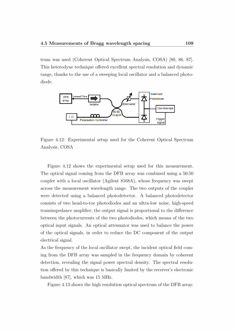
4.5 Measurements of Bragg wavelength spacing 109
trum was used (Coherent Optical Spectrum Analysis, COSA) [80, 86, 87].
This heterodyne technique offered excellent spectral resolution and dynamic
range, thanks to the use of a sweeping local oscillator and a balanced photo-
diode.
Figure 4.12: Experimental setup used for the Coherent Optical Spectrum
Analysis, COSA
Figure 4.12 shows the experimental setup used for this measurement.
The optical signal coming from the DFB array was combined using a 50:50
coupler with a local oscillator (Agilent 8168A), whose frequency was swept
across the measurement wavelength range. The two outputs of the coupler
were detected using a balanced photodetector. A balanced photodetector
consists of two head-to-toe photodiodes and an ultra-low noise, high-speed
transimpedance amplifier; the output signal is proportional to the difference
between the photocurrents of the two photodiodes, which means of the two
optical input signals. An optical attenuator was used to balance the power
of the optical signals, in order to reduce the DC component of the output
electrical signal.
As the frequency of the local oscillator swept, the incident optical field com-
ing from the DFB array was sampled in the frequency domain by coherent
detection, revealing the signal power spectral density. The spectral resolu-
tion offered by this technique is basically limited by the receiver’s electronic
bandwidth [87], which was 15 MHz.
Figure 4.13 shows the high resolution optical spectrum of the DFB array.

4.5 Measurements of Bragg wavelength spacing 110
Figure 4.13: High resolution spectrum measured using a Coherent Optical
Spectrum Analyser
All the DFBs were pumped at 100 mA, well above the threshold. As visible
in the main horizontal axis, the designed frequency spacing of 20 GHz was
maintained also above the threshold. The DFB one, on the left side, was
still a bit closer. The high resolution of this technique allowed the measure-
ment of the obtained spacing accuracy. Taking the DFB two (central line)
as reference, DFB one was 19.5 GHz spaced, while DFB three was 19.9 GHz
spaced.
The secondary horizontal axis gives an idea of the Bragg wavelength thermal
shift when the gratings were biased at high currents. From the below thresh-
old situation, the Bragg wavelength red shifted of 0.75 nm. This shift does
not represent a problem, since, if necessary, it can be easily compensated by
decreasing the operative temperature of the lasers.
The method used to manufacture grating with high precision wavelength
spacing showed a very high accuracy. In all the gratings used in the final
devices for the mm-wave generation, the Bragg wavelengths were varied only
by changing their waveguide widths. Moreover, the high accuracy achieved

4.6 Stability measurements 111
suggested their in multi wavelength DFB arrays for DWDM applications
[58, 59].
4.6 Stability measurements
As final test, the DFBs were evaluated with respect to their operational
stability over the time. The test was not performed to measure their overall
life time, but in order to check the reliability of their basic lasing charac-
teristics over a limited period of time. A life time of few hundreds of hours
was considered adequate to prove the concept of mutual injection locking
assisted by four wave mixing using the integrated devices. During that time,
the basic lasing characteristics, such as output power single mode operation
and wavelength tunability, had to be maintained.
A basic characterisation of the laser was firstly performed as a reference, mea-
suring their wavelength maps, L-I and V-I characteristics. After that, the
DFB was biased at 50 mA, three times the threshold current, for about 150
hours continuously; the temperature controller stage was set at 20 C. The
output power and p-n junction voltage were automatically measured every
10 seconds. Both the measured parameters were extremely stable over the
whole period of time, exhibiting a variation smaller than 0.5%. Wavelength
maps, L-I and V-I were measured again, and no variations were noticed.
Then, a stress test was performed, in order to check its parameters after a
period of operation under extreme conditions, simulating the device ageing.
The laser was biased at 170 mA, ten times the threshold current, and the
temperature was set at 50 C; this condition was continuously maintained
for 75 hours. The device was able to stand the test, but, as expected, their
lasing characteristics slightly degraded. Figure 4.14 shows the P-I, L-I and
wavelength maps before and after the tests.
The lasing characteristics were totally unchanged after the first 150 hours
of operation under normal condition. After the simulated ageing, the lasers
were still working properly, but exhibited a higher threshold current (from
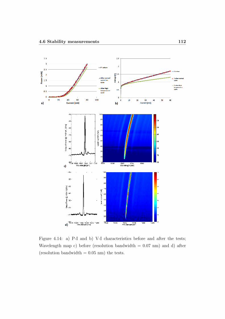
4.6 Stability measurements 112
Figure 4.14: a) P-I and b) V-I characteristics before and after the tests;
Wavelength map c) before (resolution bandwidth = 0.07 nm) and d) after
(resolution bandwidth = 0.05 nm) the tests.

4.6 Stability measurements 113
17 to 25 mA) and a lower junction voltage. The wavelength map shows that
the single mode operation was preserved, but the DFB showed a smaller
wavelength tunability with respect of the injected current. These changes
are related to a general degradation of the quantum wells and of the overall
crystal quality, due to the high current and temperature applied during the
test.
From the results of these measurements, the devices were considered abso-
lutely reliable and stable during the whole testing period, allowing long char-
acterisations without the need of any recalibration of the lasing parameters
over the time.
Chapter 5
Mutual Injection-Locking
experiments
In this Chapter the mutual injection locking experiments are described.
The Chapter is divided in three Sections, where the locking of two and three
lasers is analysed, and where the FWM efficiency is characterised.
Section 5.1 focuses on the mutual injection locking of two DFBs, that are
directly coupled and emit at the same optical frequency. It is shown that
the locking is accompanied by the linewidth narrowing of the two lasers. A
Section where the FWM efficiency is characterised follows (Section 5.2).
In the second part of the Chapter (Section 5.3) the mutual injection locking
of three DFBs operating at three different frequencies is analysed. After
a brief introduction on the device geometries used for the experiment, the
methodology used to phase-lock the lasers is discussed. Then, the occurrence
of the locking is demonstrated, by analysing three different aspects: i) the
presence of a locking range; ii) the optical linewidth reduction; iii) the phase
noise reduction of the generated mm-wave electrical signal. It is also shown
how the generated mm-wave signal can be continuously tuned over a wide
range of frequencies. The electrical linewidth of the generated mm-wave
signal is analysed with respect to its frequency and to the mutual injection
strength. Finally, investigations to demonstrate the locking of the lasers up

5.1 Mutual injection-locking of two DFBs 115
to hundreds of GHz of detuning are presented.
5.1 Mutual injection-locking of two DFBs
The locking measurements began from the mutual injection locking of two
DFB lasers operating at the same frequency. This situation was interesting
as it simulates the injection locking assisted by FWM. It helped to define the
range of optical attenuation required between the two lasers and to assess
the dependence of the locking range on the mutually injected power.
The optical injection locking is a well-known phenomena, since it represents
an effective method to synchronise one or several optical oscillators to a
master laser [88–91].
Figure 5.1: Injection locking configurations: a) Master-Slave injection, b)
Mutual injection.
In classical master-slave-type injection locking (Figure 5.1a), a slave laser
is injected by a master laser via an optical isolator. The slave laser locks
to the master frequency when their oscillation frequencies are close enough.
In the mutual injection configuration (Figure 5.1b) the optical isolator is re-
moved: the configuration is symmetrical and it is thus impossible to define
a master and a slave laser [92]. The symmetry is broken for the case where
one laser emits more power than the other. The laser that emits the larger
optical power behaves like a master laser, as the other one senses a larger
injection, and thus behaves as the slave laser. If the frequencies of the two
lasers are close enough, the slave laser is forced to oscillate at the master
frequency, and its phase is locked to that of the master. When the two lasers

5.1 Mutual injection-locking of two DFBs 116
are locked, their oscillations are synchronised and they represent a stable op-
tical system. As a consequence, their optical linewidth narrows once a stable
locking condition is reached [92].
As discussed in the above mentioned papers, different locking conditions can
be achieved depending on the amount of injected power. Large levels of op-
tical injection may lead to an unstable locking situation, while too low levels
do not allow the occurrence of the locking between the two lasers.
Another very important parameter which strongly depends on the mutu-
ally injected power is the locking range. It can be defined as the interval
during which the two lasers are phase-locked and operating at the same fre-
quency, while the operating frequency of one of them is increased by tuning
its biasing current. It is measured in GHz, considering the typical laser’s
frequency/current tuning of 3 GHz/mA. The optimal operation conditions
of two mutually injected lasers require a trade-off between locking range and
injected power, in order to achieve a sufficient wide locking range without
leading to an unstable locking condition.
The experimental measurements were carried out on the devices Design 3
(Figure 2.1): DFB-3 and DFB-2 were mutual injected, while the DFB-1 and
the attenuator between DFB-1 and DFB-3 were strongly reverse biased (-3
V) to avoid any unwanted back reflection from the adjacent grating. The
DFB-2 was biased at 79 mA, while the DFB-3 current was swept from 92
mA to 103 mA in order to tune its operating wavelength, and make it cross
the operating wavelength of DFB-2. Different values of the injection levels
were obtained by reverse biasing the attenuator between DFB-2 and DFB-3,
from -1.8 V to -2.15 V. The optical signals were collected using a lensed op-
tical fibre from the output tapered waveguide next to DFB-2, and both the
optical and RF spectra were recorded. Figure 5.2 shows the locking maps (in
terms of optical and RF spectra) when the attenuator between the lasers was
biased at -1.8 V, which corresponds to an optical attenuation of 35 dB. The
attenuation values were calculated from a set of available data of the gain
spectra of the used semiconductor material, measured using the Hakki-Paoli

5.1 Mutual injection-locking of two DFBs 117
method [93].
Figure 5.2: Locking maps with attenuator biased at -1.80 V, showing optical
(upper-left panel) and electrical (upper-right panel) spectra for increasing
current of DFB-3. The vertical scale of both maps is dBm, and represents
respectively the optical and electrical power. The panels in the bottom row
show the RF spectra corresponding to different situations.
Looking at the optical spectrum, we notice that, starting from the bot-
tom, DFB-2 was represented by the powerful peak at 1552.6 nm, while the
DFB-3 was 1552.4 nm, approaching DFB-2 when its current was increased.
Looking at the electrical spectrum, at point A only one peak was present,
which corresponds to the beating between DFB-2 and DFB-3. The two lasers
were in the so-called free-running regime.
At point B, the distance between DFB-3 and DFB-2 was equal to their re-

5.1 Mutual injection-locking of two DFBs 118
laxation oscillation frequency (10.2 GHz). Since DFB-3 was superimposed
to one of the relaxation sidebands of DFB-2 (and vice versa), DFB-3 and
DFB-2 could achieve a mutual phase-locking via their relaxation oscillation
peaks. For a certain DFB-3 current range (92.6 to 95.2 mA, corresponding
to a variation of its lasing frequency of 1.8 GHz) their frequency distance
was stable and locked, and several secondary FWM products were visible in
the optical spectrum. A clear and narrow peak at 10.2 GHz was visible in
the electrical spectrum. The second harmonic at 20.4 GHz was due to the
beating of the secondary FWM products. Although this situation is very in-
teresting, it is not useful with a view to the generation of tunable mm-wave
signals, since it cannot be tuned by more than few tens of MHz.
By further increasing DFB-3 current (situation C ), the lasers were locked
and operating at the same frequency. However, due to the strong levels of
injections, the locking was very unstable, as revealed by the several broad
peaks visible in the RF spectrum.
In D, the two lasers were too far, and the injected power was not enough
to make them lasing at the same frequency. As consequence, the two lasers
unlocked. The residual peak at the relaxation oscillation frequency was due
to the strong injection of DFB-3 in proximity of the relaxation sideband of
DFB-2.
Due to its high instability, the condition of point C should be avoided for
the sake of a proper operation of the devices for the mutual injection locking
assisted by FWM: it would not allow the generation of a RF signal with high
spectral purity.
A more stable locking could be achieved by increasing the attenuation be-
tween the two lasers, thus reducing the mutual coupling strength. Figure 5.3
shows the locking maps when the attenuator was biased at -1.91 V, equivalent
to an attenuation of 38 dB.
The situations represented by points A occurred for different values of
DFB-3 current. DFB-3 was simply approaching (or moving away from) DFB-
2: the lasers were unlocked, and their broad-linewidth beating signal has
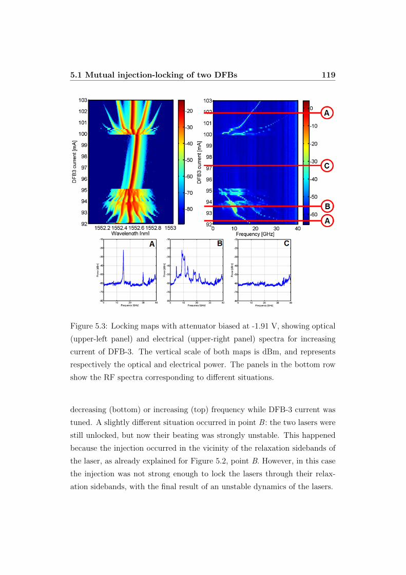
5.1 Mutual injection-locking of two DFBs 119
Figure 5.3: Locking maps with attenuator biased at -1.91 V, showing optical
(upper-left panel) and electrical (upper-right panel) spectra for increasing
current of DFB-3. The vertical scale of both maps is dBm, and represents
respectively the optical and electrical power. The panels in the bottom row
show the RF spectra corresponding to different situations.
decreasing (bottom) or increasing (top) frequency while DFB-3 current was
tuned. A slightly different situation occurred in point B : the two lasers were
still unlocked, but now their beating was strongly unstable. This happened
because the injection occurred in the vicinity of the relaxation sidebands of
the laser, as already explained for Figure 5.2, point B. However, in this case
the injection was not strong enough to lock the lasers through their relax-
ation sidebands, with the final result of an unstable dynamics of the lasers.

5.1 Mutual injection-locking of two DFBs 120
By further increasing DFB-3 current, a stable locking occurred (Figure 5.3,
point C ). As shown in both optical and spectrum maps, the two lasers col-
lapsed into a single lasing frequency regime. This is a nice mutual locking
condition, in which the two lasers were perfectly synchronised: only one
mode was visible in the optical map, and no RF beating was present in the
RF map (i.e., the beat signal shifts down to DC, or zero frequency). The
two lasers remained locked for a wide range of values of DFB-3 current.
Within the locking range, the increase of DFB-3 current only had the effect
of dragging the DFB-2 peak towards higher wavelengths. By considering a
wavelength tuning of DFB-3 in free-running regime of 24 pm/mA, equiva-
lent to 3 GHz/mA (from Figure 4.3), the locking range width was around 14
GHz. Such a wide locking range was due to the high injection levels. Insta-
bility and excitation of the relaxation sidebands were avoided thanks to the
increased optical losses provided by the attenuator. As in the previous case,
DFB-2 came back to its unperturbed frequency once the locking regime was
over.
The locking range is expected to decrease for a further increase of the optical
attenuation between the lasers. Figure 5.4 shows the locking maps with the
attenuator biased at -2.2 V, giving 42 dB of optical attenuation.
Due to low levels of injection, DFB-3 was approaching DFB-2 without
disturbing it, even when their frequency distance was close to their relaxation
oscillation (points A); the RF spectrum shows the beating of the two lasers.
Once DFB-3 was superimposed to DFB-2, the locking occurred (point B).
However, due to the strong attenuation between the lasers, the locking range
was limited to 3 GHz, which is a much smaller amount than that achieved
with an attenuation of 38 dB. When the mutual coupling is weak, it cannot
force the two lasers to work as a single synchronised system.
The locking was not achieved for higher levels of optical attenuation between
the lasers. The lasing mode of DFB-3 simply crossed the DFB-2 mode, and
no locking range could be observed. The complete results for the range width
as function of the attenuation between the lasers are summarised in Figure

5.1 Mutual injection-locking of two DFBs 121
Figure 5.4: Locking maps with attenuator biased at -2.30 V, showing optical
and electrical spectra for increasing current of DFB-3. The insets show the
RF spectrum in different situations.
5.5.
Depending on the attenuation between the lasers, three different operat-
ing regimes could be found. For low levels of attenuation, an unstable locking
regime was achieved. The mutual injection was too strong to allow a stable
operation of the compound laser system. Such high levels of optical injection
can lead not only to an unstable dynamics of the lasers, but can even drive
the lasers to operate in a chaotic regime. Although a wide locking range can
be achieved, this regime cannot be exploited for the mutual injection locking
due to its inherent instability. For attenuations between 37 to 42 dB, a sta-
ble locking regime was achieved. The lasers where locked to each other, and
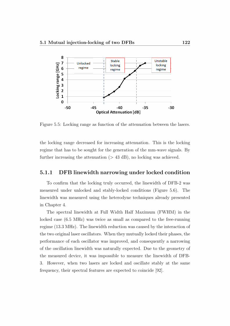
5.1 Mutual injection-locking of two DFBs 122
Figure 5.5: Locking range as function of the attenuation between the lasers.
the locking range decreased for increasing attenuation. This is the locking
regime that has to be sought for the generation of the mm-wave signals. By
further increasing the attenuation (> 43 dB), no locking was achieved.
5.1.1 DFB linewidth narrowing under locked condition
To confirm that the locking truly occurred, the linewidth of DFB-2 was
measured under unlocked and stably-locked conditions (Figure 5.6). The
linewidth was measured using the heterodyne techniques already presented
in Chapter 4.
The spectral linewidth at Full Width Half Maximum (FWHM) in the
locked case (6.5 MHz) was twice as small as compared to the free-running
regime (13.3 MHz). The linewidth reduction was caused by the interaction of
the two original laser oscillators. When they mutually locked their phases, the
performance of each oscillator was improved, and consequently a narrowing
of the oscillation linewidth was naturally expected. Due to the geometry of
the measured device, it was impossible to measure the linewidth of DFB-
3. However, when two lasers are locked and oscillate stably at the same
frequency, their spectral features are expected to coincide [92].

5.2 FWM efficiency 123
Figure 5.6: Spectral linewidth of DFB-2 under a) unlocked and b) locked
conditions.
5.2 FWM efficiency
In the mutual injection locking assisted by FWM, the locking should
occur via the mutual injection of FWM clones generated in a third laser.
When the locking condition is satisfied (ν3 = ν1+ν22
, Section 1.4), DFB-2 is
injection-locked by the FWM clone of DFB-1, and vice versa. Therefore, it
is important to measure the FWM efficiency in producing these clones, in
order to assess the effective mutual coupling occurring between the two lasers
that operate at different optical frequencies. This effective coupling shall be
compared with the coupling values that gave rise to mutual phase-locking of
two DFBs (as shown in Section 5.1).
The device Design 3 was employed to characterise the FWM gain. DFB-
2 was biased at 110 mA, and the current of DFB-3 was swept in order to
measure the FWM gain at different detunings, meant as frequency spacing
between the lasers. FWM gain can be defined as:
FWMgain =P (ν ′3)
P (ν3)
where P (ν3) is the power injected into DFB-2 by the laser DFB-3, and

5.2 FWM efficiency 124
P (ν ′3) is the power of the FWM clone generated by the interaction of DFB-2
and DFB-3, located at the frequency ν ′3 = 2ν2− ν3. The attenuator between
DFB-2 and DFB-3 was biased at -1.95 V, in order to avoid the rise of unstable
lasing dynamics, while the attenuator 1-3 and DFB-1 were strongly reverse
biased at -3 V to avoid any unwanted back reflections. The light was collected
from the output waveguide on the DFB-2 side. Figure 5.7a shows the optical
spectrum of the signal collected from the DFB-2 output waveguide.
Figure 5.7: Conversion efficiency (FWM gain) characterisation. a) Optical
spectrum b) FWM gain as a function of the detuning of the injected signal.
The optical power of the FWM clones exhibited a strong dependence on
the detuning between the pump (DFB-2) and the probe (DFB-3) signals.
For small detuning, the probe and the FWM clone signals had almost the
same power; then, by increasing the detuning between the lasers, the power
of the FWM clones rapidly dropped. Figure 5.7b shows the FWM gain as
a function of the detuning. The FWM process was very efficient for small
detunings (up to 10 GHz), where it was possible to generate clones having
almost the same power of the injected signal. Then, for larger frequency
detuning, the efficiency decreased. However, the efficiency did not decrease
following a logarithmic trend as expected. As described also in [94], when a
DFB laser biased above threshold is used as mixing medium, the generation

5.2 FWM efficiency 125
of FWM products depends on the interaction of different factors. Referring
to our case, the incident probe signal (DFB-3) was partially back reflected by
the stop band of DFB-2: depending on the reflectivity spectrum of the DFB-
2 grating, only a fraction of the incident light was actually injected into the
cavity of this laser. Within the cavity of DFB-2, the incident probe signal
(and also the generated FWM clone) was amplified by the gain medium.
Depending on the detuning between the lasers, there was a clear resonance
behaviour in the FWM gain. The DFB-2 cavity enhanced differently the light
passing through it, following the reflectivity spectrum of its grating. When
the lasers where operating at very close frequencies, the cavity enhancement
effect was maximum, due to the high reflectivity of the grating in proximity
of its lasing frequency. Then, for increased detuning the cavity enhancement
decreased, due to the smaller values of the grating reflectivity.
Finally, in Figure 5.7b it can be also noticed that the FWM gain stabilised
at an efficiency of -35 dB once the DFB-3 fell outside the stop-band of DFB-
2, which corresponds to a detuning of around 200 GHz. The stop-band
reflectivity spectrum has several ripples, which provide a cavity enhancement
effect also for very large detunings. As it will be shown in the next Section,
this value allows for the mutual injection locking up to several hundreds of
GHz.
The FWM efficiency was measured also for the device Design 4. In this case,
the FWM takes place in an active waveguide (i.e. SOA) 1.1 mm long, and the
cavity enhancement effect is not present. The measurement was performed
as follow. DFB-3 was biased at a fixed current of 80 mA, while DFB-1 was
tuned from 75 to 93 mA. Both the 1.1 mm long SOA and the one on the
output facet were biased at 115 mA. The output signal was collected from
the straight-cleaved facet. The FWM gain is defined as in the previous case,
considering DFB-3 as pump signal and DFB-1 as probe signal. Figure 5.8
shows the measured FWM gain efficiency, compared with the already shown
cavity-enhanced FWM gain efficiency.
In absence of cavity enhancement effect, the FWM efficiency quickly

5.2 FWM efficiency 126
Figure 5.8: Conversion efficiency (FWM gain) in absence of cavity enhance-
ment effect. a) Optical spectrum. b) Red line: FWM gain as a function of
the detuning of the injected signal in absence of cavity enhancement effect
(Design 4 ); Blue line: FWM gain as a function of the detuning of the in-
jected signal in presence of cavity enhancement effect (measured on Design
3 ).
drops, with the FWM clones drown in the spontaneous emission floor af-
ter a few GHz of detuning. Higher efficiency could be obtained by pumping
the active section with larger currents. However, this was not possible due
to the geometry of the device. At the edges of the SOA in which the FWM
process takes place there are reflective elements: the cleaved facet on the
right side and the three gratings on the left side. This structure acts as an
additional multimode optical cavity, which reaches the lasing threshold when
the SOA is strongly pumped. Since this situation is to be avoided, the FWM
conversion efficiency achievable with this device geometry is very low, and
it is non-negligible only for small detunings. As will be shortly discussed,
this poor FWM gain represented one of the problem in order to obtain the
mutual injection locking using the device Design 4.

5.3 Mutual injection-locking of three DFBs assisted by FWM 127
5.3 Mutual injection-locking of three DFBs
assisted by FWM
In this section the experimental results for the mutual injection locking
assisted by FWM are presented. The four different device geometries intro-
duced in Chapter 2 (Figure 2.1) were tested, in order to define which is the
most promising design. The devices Design 1, 2, 3 share the same principle
of operation, with DFB-1 and DFB-2 coupled into DFB-3: different coupling
strengths are obtained by using different couplers (1% evanescent coupler for
Design 1, 50% MMI coupler for Design 2 and direct injection for Design 3 )
and by biasing the SOA/attenuators between the lasers. Design 4 is based
on a different principle of operation, since the three DFBs are injected via a
MMI coupler into a long SOA, where the FWM process occurs. The optical
reflection necessary for the mutual injection mechanism is provided by the
straight cleaved facet located at the right-hand side of the device.
Design 1, 2, 3 showed very similar results. The mutual injection locking
was successfully achieved using all the three geometries. However, depend-
ing on the detuning between the lasers, the SOA/attenuators were used to
adjust the injection levels. As discussed in Section 5.2, the FWM efficiency
decreases for increasing detuning. For small detuning, the FWM clones are
very powerful, and therefore a smaller coupling factor (i.e. a larger attenua-
tion) is preferable. Design 1 exhibited the best results for small detunings,
up to a few GHz. Then, at higher detuning the optical amplification pro-
vided by the SOAs, necessary to countervail the lower FWM efficiency, was
not sufficient to obtain a stable locking.
Design 2 proved to be the best geometry. Stable locking was reached for a
wide range of detunings: most of the results shown in the next Sections were
obtained using this device. Both SOA/attenuators and MMI coupler could
be direct- or reverse-biased in order to obtain the proper levels of injection,
allowing a very wide range of tunability of the generated mm- wave signal.
Due to the limited bandwidth of the available RF spectrum analyser (Rohde

5.3 Mutual injection-locking of three DFBs assisted by FWM 128
& Schwarz FSV40, 40 GHz bandwidth), the locking properties were charac-
terised for frequencies up to 40 GHz.
Design 3 was used to demonstrate the mutual injection locking at high fre-
quencies, where the FWM efficiency is small and therefore high level of injec-
tion were required. However, by strongly reverse-biasing the SOA/attenuators,
the phase-locking condition was obtained also for detunings of a few GHz.
Unlike all the other designs, no mutual injection locking was demonstrated
using the device Design 4. The main explanation for the above is the ab-
sence of the cavity enhancement for the FWM process, with a consequent
low FWM efficiency. Moreover, in Design 4 was not possible to adjust the
levels of injection for each laser separately, and consequently the complex
dynamics of the device could not be well controlled. Due to these reasons,
after the unsuccessful initial investigation, this device was no longer used for
the demonstration of the mutual injection locking assisted by FWM.
Finally, Figure 5.9 shows the experimental setup used to characterise the
mutual injection locking and the optical linewidth of the DFB lasers.
Figure 5.9: Experimental setup used for the characterisation of the devices.
The optical signal generated by the Device Under Test (DUT) was col-
lected using special lensed optical fibres (OZ optics TSMJ-3A-1550-9/125-
0.25-7-5-26-2-AR), followed by an optical isolator, used in order to avoid
backreflections from the straight fibre optic connectors that could spoil the
correct operation of the devices. The light was then split in two paths, us-
ing a 90/10 optical coupler. The 90% output was connected to an optical
amplifier (OptoSci EDFA-S51052) and then to the high speed photodetector

5.3 Mutual injection-locking of three DFBs assisted by FWM 129
(U2t Photonics XPVD3120R) for the generation of the mm-wave signal. Its
output signal was amplified by a high speed low noise amplifier (Centellax
TA0L50VA) and then measured using a RF spectrum analyser (Rohde &
Schwarz FSV40). The 10% output of the coupler was used to check the op-
tical spectrum of the collected signal, using an Optical Spectrum Analyser
(Advantest Q8384). The second input port of the optical coupler was con-
nected to an external tunable laser (Agilent 8164A), to measure the optical
linewidth of the lasers using the heterodyne technique presented in Section
4.2. A polarisation controller was used to maximise the coherent detection
efficiency.
5.3.1 Methodology and demonstration of the phase lock-
ing
The characterisation process started from demonstrating the possibility of
achieving the mutual injection locking using the integrated devices. The De-
sign 2 device was firstly used. In fact, thanks to the multiple SOA/attenuators
and contacted MMI coupler, it allowed a very wide tunability of the injection
levels.
The mutual injection locking of three lasers was verified as follow. DFB-1
and DFB-2 were pumped at fixed currents, respectively at 85.24 and 82.7
mA, while the DFB-3 current was finely tuned around 92.5 mA in order to
reach the locking condition ν3 = ν1+ν22
. The attenuators were biased at trans-
parency (11 mA) and the MMI was used as attenuator, biasing it at -0.2 V.
From Figure 5.10 to 5.13 the evolution of the optical and electrical spectra
(respectively on the left- and right-hand sides) during the tuning of DFB-3
current is shown.
In Figure 5.10 the locking condition was not verified. Since DFB-3 was
not centred between DFB-1 and DFB-2, a large number of FWM products
are visible in the optical spectrum. However, due to the high number of
optical peaks and the limited resolution of the optical spectrum analyser (0.01
nm, 1.25 GHz) the locking dynamics cannot be fully understood. The RF

5.3 Mutual injection-locking of three DFBs assisted by FWM 130
Figure 5.10: Evolution of the signal’s optical and electrical spectra during
the tuning of DFB-3 current: locking condition not verified.
spectrum shows more informations about this case. The relative frequency
distance between DFBs-1-3 and DFBs-3-2 was unequal, and therefore their
electrical beatings had different frequencies. The two highest RF peaks are
the beating between the above-mentioned couples of lasers. A large number
of additional RF peaks are present, due to the multiple beatings between
the other several FWM products visible in the optical spectrum. The RF
linewidth of all these peaks is rather wide, since the lasers were in a free
running regime and no phase correlation was achieved. The small peak at
around 38 GHz represents the beating between the lasers DFB-1 and DFB-2.
In Figure 5.11 the locking condition was close to being satisfied. DFB-3
is lasing very close to the mid-point frequency between DFB-1 and DFB-2.
In the optical domain, only the three lasers and two supplementary FWM
products are visible. The latter are due to the interaction between DFB-1
and DFB-3 inside the DFB-1 cavity (as well as for DFB-2 with DFB-3 in
DFB-2 cavity), but these modes do not participate in the mutual injection
locking mechanism. In the electrical domain, it is possible to observe that
the beatings DFB-1-3 and DFB-3-2 are almost superimposed. However, since
the locking condition was not exactly matched, the RF peak at 20 GHz is
still broad. All the other FWM sub-products are hidden under the wide RF

5.3 Mutual injection-locking of three DFBs assisted by FWM 131
Figure 5.11: Evolution of the signal’s optical and electrical spectra during
the tuning of DFB-3 current: locking condition almost verified.
peak.
By slightly increasing the current of DFB-3, the locking condition was
achieved (Figure 5.12). Since the main FWM products (ν ′1 and ν ′2 as de-
scribed in Chapter 1) are now exactly superimposed to DFB-1 and DFB-2,
the optical modes visible in optical domain are narrower. Moreover, due to
strong levels of mutual injection, small peaks at the relaxation frequency of
Figure 5.12: Evolution of the signal’s optical and electrical spectra during
the tuning of DFB-3 current: locking condition verified.
5.3 Mutual injection-locking of three DFBs assisted by FWM 132
DFB-3 appeared. The RF spectrum shows two main narrow peaks, at the
frequencies ν3− ν1 = ν2− ν3 and ν2− ν1 (in Figure 5.12 these correspond to
frequencies 19.1 GHz and 38.2 GHz). The narrowing of the peak at 38.2 GHz
is hard to notice due to its low power. On the other hand, the narrowing of
the first peak is remarkable. The peak is sharply narrower than any peak
seen in the unlocked condition. This stable locked situation was maintained
during the tuning of DFB-3 for almost 1 mA, implying the existence of a
locking range of 3 GHz width.
Figure 5.13: Evolution of the signal’s optical and electrical spectra during
the tuning of DFB-3 current: locking condition not verified.
Figure 5.13 shows a similar situation to the one already seen in Figure
5.10. The locking condition was no longer satisfied, and DFB-3 was now
lasing closer to DFB-2. A large number of FWM products and relative beat-
ings are visible, respectively, in the optical and electrical spectra. As noticed
before, the electrical linewidth of the beating signals is significantly larger
than under locked condition.
The full locking sequence can be viewed in two videos that are available on-
line1,2: the videos show the RF spectra for increasing values of DFB-3 cur-
rent, with RF spans of 40 GHz and 5 GHz, respectively. The beating signals
1http://www.youtube.com/watch?v=jGF5XlDWFFU2http://www.youtube.com/watch?v=URqOs-9Zxcc

5.3 Mutual injection-locking of three DFBs assisted by FWM 133
approach each other, then the locking occurs and is maintained during the
whole locking range, and finally the lasers unlock and the two distinct beat-
ing signals can again be observed. The linewidth narrowing of the generated
RF signal and the existence of a wide locking range can be well appreciated.
In order to measure the linewidth reduction of the electrical signals, the RF
spectrum was measured using smaller span (5 GHz and 500 MHz) and ap-
propriate resolution bandwidth (300 kHz). Figure 5.14 shows the beating
signals in unlocked and locked conditions.
Figure 5.14: Generated RF signal under a) unlocked and b) locked conditions,
shown with a RF span of 5 GHz. In c) a span of 500 MHz allows for the
precise measurement of the electrical linewidth.
Figure 5.14a shows the beating signals between the lasers DFB-1 and
DFB-3, on the left at 10 GHz, and DFB-3 and DFB-2, on the right at 13.3
GHz. Since the lasers are not phase locked, the fluctuation of their instan-
taneous emission frequency are not correlated and therefore the electrical
beating is a broad linewidth signal. The measured linewidth FWHM for the
RF signal in unlocked conditions was 47 MHz.
Figure 5.14b shows the beating when the locking condition was satisfied: the
beating linewidth is clearly narrower. Figure 5.14c shows the same electri-
cal signal but with a span of 500 MHz, in order to precisely measure its
linewidth. The beating linewidth is now 2.1 MHz, showing a reduction of
a factor 20 from the unlocked condition. The sidebands visible at 50 MHz
and 100 MHz from the peak are due to an unwanted electrical modulation

5.3 Mutual injection-locking of three DFBs assisted by FWM 134
coming from the laser driver used to pump the three DFBs. By using low
pass filters this unwanted modulation was strongly reduced: the sidebands
are respectively 30 and 35 dB smaller than the peak, and did not involved
problems during the locking measurements. However, particular attention
was paid in order to precisely measure the linewidth of the beating signals.
The condition of mutual injection locking was further confirmed by three
different indicators:
• Presence of a clear locking range.
• Optical linewidth reduction of each laser.
• Phase noise reduction (linewidth reduction) of the RF beating signal
These indicators are discussed below.
Presence of a clear locking range When the mutual injection locking
occurred, the three lasers maintained a stable locked condition even if the
current of DFB-3 was increased. Once the locking condition is satisfied, the
locking range can be defined as the tuning interval of the DFB-3 current
that allows the three DFBs to be stably phase-locked. It is measured in
GHz, considering its frequency/current tuning of 3 GHz/mA.
Figure 5.15 show the maps of optical and electrical spectra during the
mutual injection locking. These maps were obtained by polarising the DFBs
very close to the locking condition (DFB-1 = 81.1 mA, DFB-2 = 82.6 mA,
DFB-3 ' 83 mA), the SOA/attenuators were biased at transparency and the
MMI coupler was biased at -0.2 V, providing an attenuation of 12.4 dB. As
starting point, DFB-3 was biased at 82.9 mA, in order to have the electrical
beatings between the lasers DFB-1-3 and DFB-3-2 less than 5 GHz apart.
The tuning of the beating signals is visible as powerful red-yellow lines, while
the other RF peaks (light blue lines) are due to the multiple beatings be-
tween the other several FWM products visible in the optical spectrum. This

5.3 Mutual injection-locking of three DFBs assisted by FWM 135
Figure 5.15: Maps of a) optical and b) electrical spectra during the mutual
injection locking. The vertical scale represents the power of the signals,
expressed in dBm.
situation is the same already described for Figure 5.10. Then, by increasing
the DFB-3 current, the locking condition was satisfied: the two electrical
beatings approached each other, till when, at DFB-3 current = 83.2 mA, the
locking occurred. The locking was stable for about 0.7 mA of DFB-3 current
tuning (which correspond to a locking range of 2.1 GHz), during which the
linewidth of the beating signal narrowed; this condition is the same already
described in Figure 5.12. Finally, when DFB-3 current was set to 83.85 mA,
the locking condition was no longer satisfied, and two broad RF peaks were
visible again.
The presence of a locking range is a clear sign that the locking occurred. In
absence of locking the two electrical beatings would have simply crossed each
other, drawing a sort of ”X”-shaped locking map in the plane Frequency -
DFB-3 current. During the locking range, the distance between the lasers
was quasi-constant even if the current of DFB-3 was increased. A small
variation of the beating frequency is due to a slightly unbalanced mutual
injection, since the lasers were operating at different currents. Finally, as it

5.3 Mutual injection-locking of three DFBs assisted by FWM 136
will be discussed in Section 5.3.3, the locking range strongly depends on the
injected power.
Optical linewidth reduction The geometry of Design 2 allowed the mea-
surement of the optical linewidth of each individual DFB, under locked and
unlocked conditions. When the locking condition was not satisfied, the opti-
cal linewidth of each laser was 13 MHz, as previously described in case of two
unlocked mutually injected lasers (Section 5.1.1). Once the mutual injection
locking was achieved, the optical linewidth narrowed. Figure 5.16 reports
the optical linewidth of the three lasers measured under locking conditions,
measured using the heterodyne method.
Figure 5.16: DFB’s optical linewidth under locked conditions. a) DFB-1, b)
DFB-2, c) DFB-3. The linewidth of all the lasers narrowed down to 6 MHz.
The linewidth of all the lasers narrowed down to 6 MHz. This reduc-
tion represents another clear evidence that the mutual injection locking took
place. DFB-1 and DFB-2 where mutually injected by the FWM clones gen-
erated in DFB-3. The linewidth reduction occurred, similarly to the case of
two mutually injected lasers (Section 5.1.1). However, the most meaning-
ful evidence that all the lasers were locked together is the narrowing of the
linewidth of DFB-3. The locking mechanism explained in Section 1.4 oc-
curred. DFB-3 was not injected at its lasing frequency by any laser or FWM
clone, but only by the modulation sidebands due to the detuned mutual in-
jection. In fact, as already shown in Figure 1.8, when the locking condition

5.3 Mutual injection-locking of three DFBs assisted by FWM 137
is satisfied the carrier density of each laser is modulated at the frequency
ν31 = ν23 = (ν3− ν1) = (ν2− ν3). Strong modulation sidebands rise sideways
each lasing mode. In particular, the higher frequency sideband of DFB-1
and the lower frequency sideband of DFB-2 inject DFB-3, phase-locking it
to them.
Phase noise reduction Once the three lasers are locked, the RF signal
produced by the photomixing in a suitable detector/antenna is expected
to exhibit better performances. This improvement mainly concern the fre-
quency stability of the generated RF signal, with respect to the conventional
case where two uncorrelated lasers are used. In particular, the locked system
exhibits reduced short-term random fluctuations of the signal’s frequency.
These fluctuations are expressed by the phase noise of the generated electri-
cal signal. This parameter is measured in the frequency domain, and can be
described as a ratio of signal power to noise power measured in a 1 Hz band-
width at a given offset from the desired signal; it is expressed in dBc/Hz at
a given frequency offset from the carrier [95, 96]. Finally, it is characterised
by measuring the noise sidebands on one side of the signal center frequency
(Single Side Band phase noise, SSB).
The phase noise of the photomixing signal was characterised under unlocked
and locked conditions. The measurements were performed using the built-in
phase noise measurement capability of the RF spectrum analyser (Rohde &
Schwarz FSV40).
Figure 5.17 shows the SSB phase noise sidebands of the photomixing sig-
nal. Under unlocked conditions, the instantaneous frequency of the electrical
signal was unstable, and therefore its power was spread over a number of
frequencies in the vicinity of the center frequency. This resulted in a high
frequency cut-off of the noise sideband. Once the locking condition was
achieved, the phase noise decreased. The smaller cut-off frequency of the
measured noise sideband demonstrate that the photomixing signal was more
stable, as it was affected by smaller frequency fluctuations.

5.3 Mutual injection-locking of three DFBs assisted by FWM 138
Figure 5.17: SSB phase noise measurement for the photomixing signal when
the lasers were in unlocked and unlocked conditions
This phase noise reduction is a further proof that the overall frequency sta-
bility of the system is enhanced when the locking condition is satisfied.
5.3.2 Tunability of the RF signal
The mutual injection locking assisted by FWM is an improvement of the
simple photomixing technique, and therefore it is expected to preserve one
of its most important advantages: the wide and continuous frequency tun-
ability of the generated RF electrical signal. The mutual injection locking
can be achieved over a very wide range of detunings between the lasers, as
long as the locking condition is satisfied and the mutually injected FWM
clones have the right levels of power to stably lock the lasers. Thus, the
photomixing signal can be tuned by biasing the three DFBs at different cur-
rents, in order to modify their relative frequency spacing while maintaining
the locking condition.
Thanks to the quasi-continuous tunability of the DFBs current, a very
fine tunability of the photomixing signal was achieved (Figure 5.18a). The
smallest achievable step of frequency tunability was limited by the tuning

5.3 Mutual injection-locking of three DFBs assisted by FWM 139
Figure 5.18: a) Fine and b) coarse tunability of the photomixing signal
resolution of the current drivers used to bias the DFBs. The laser driver
used was a Newport 8000, which allowed a current tuning step of 0.01 mA.
The photomixing signal was finely tuned in steps of only 30 MHz: this value
is due to the laser frequency tunability previously described (24 pm/mA = 3
GHz/mA). The fine tuning step can be further reduced by using laser drivers
with an even higher current tuning resolution.
The locking condition was achieved over a wide range of detunings, allowing
a wide tunability of the photomixing signal. Figure 5.18b shows that the
photomixing signal could be precisely tuned all over the available bandwidth
of the RF spectrum analyser (0-40 GHz); in Section 5.3.6 is shown that the
mutual injection locking was also achieved at higher frequencies (160 GHz
and 280 GHz).
The frequency tunability is limited at lower and higher frequency values due
to different causes. The upper limited is set by the FWM efficiency. Thanks
to the cavity enhancement effect, FWM clones with enough power to lock the
three lasers can be generated up to several hundreds of GHz. However, the
spectrum reflectivity ripples of the stop-band fade for detuning larger than
400 GHz (3 nm, Figure 2.15), requiring strong amplification (provided by the
SOAs) in order to reach the desired values of mutually injected power.
The low-frequency limit of the frequency tunability is potentially close to

5.3 Mutual injection-locking of three DFBs assisted by FWM 140
zero. Although the lowest mutual injection locking was achieved for detuning
between the laser equal to 5 GHz, locking at even lower frequencies can be
achieved by designing devices with stronger optical attenuators. In fact the
limiting factor here is represented by the too high mutual injection levels. For
very small detuning between the lasers, high injection levels cause unstable
or chaotic regimes of operation. In addition, it may happen that the three
lasers lock directly to each other instead of doing this through their FWM
clones: they would finally lase at one single frequency, and consequently the
photomixing signal would disappear.
5.3.3 Locking range vs. injected power
The dependence of the locking range width on the amount of injected
power was assessed also for the mutual locking assisted by FWM, as previ-
ously done for the case of mutual injection locking of two DFBs (Section 5.1).
The measurements were carried out using the device Design 2. Following the
same locking procedure described in Section 5.3.1, the DFBs were biased
close to the locking condition; then, by finely tuning the DFB-3 current, the
locking condition was reached, and the whole locking range was explored. As
introduced in Section 5.3.1, the locking range is defined as the range of values
of the DFB-3 current that allows the three DFBs to be stably phase-locked.
It is measured in GHz, considering the frequency/current tuning of DFB-3
of 3 GHz/mA. The power levels of mutual injection were changed by varying
the reverse bias applied to the MMI coupler: in this way the applied atten-
uation was the same for the injection into both DFB-1 and DFB-2. As the
attenuation provided by the MMI was sufficient, the individual attenuators
in front of DFB-1 and DFB-2 were biased at transparency. The light was
collected from the DFB-3 output and analysed using the previously described
experimental setup.
Figure 5.19 shows the maps of optical and electrical spectra during the mu-
tual injection locking, when -1.5 V were applied to the MMI coupler, yielding
an optical equivalent attenuation of 17.6 dB. DFB-1 was biased at 81.1 mA
5.3 Mutual injection-locking of three DFBs assisted by FWM 141
and DFB-2 at 82.6 mA, while the current of DFB-3 was swept from 81.8 to
83 mA. The detuning between the lasers DFB-1-3 and DFB-3-2 was around
19 GHz.
Figure 5.19: Maps of a) optical and b) electrical spectra during the mutual
injection locking with detuning between th elasers of 20 GHz. The MMI
coupler was biased at -1.5 V.
The locking condition was reached, as proven by the presence of a locking
range and a linewidth reduction of the photomixing signal between the three
lasers. However, by comparing these maps with the ones shown in Figure
5.15, it is possible to appreciate a remarkable reduction of the locking range
width. As expected, lower levels of injection lead to a smaller locking range.
When the MMI coupler was providing an attenuation of 12.4 dB the lock-
ing range was 1.8 GHz (Figure 5.15); by increasing the reverse bias at -1.5
V for an attenuation of 17.6 dB the locking range decreased to 0.2 GHz.
This happened because the FWM clones generated in DFB-3 were strongly
attenuated by the reverse-biased MMI coupler. As consequence, they were
injecting DFB-1 and DFB-2 with a weaker optical power. As already demon-
strated for the two DFBs case (Section 5.1), lower injected power leads to a
smaller locking range. In the case of three DFBs, the tuning of the current of

5.3 Mutual injection-locking of three DFBs assisted by FWM 142
DFB-3 causes a change of the optical frequencies of the FWM clones. Thus,
they cross the DFB-1 and DFB-2 modes in similar way as the tuning of one
of the lasers in the two DFBs case. With less injected power, the clones are
able to lock the DFB-1 and DFB-2 for a smaller detuning of DFB-3 from the
ideal locking condition.
By finely tuning the reverse bias applied to the MMI coupler, the dependence
of the locking range on the attenuation was characterised, and reported in
the graph of Figure 5.20.
Figure 5.20: Locking range as a function of the attenuation provided by the
MMI coupler, for detuning between the three lasers of 20 GHz.
As in the mutual injection locking of two DFBs, the locking range ex-
hibits a monotone growth when the reverse bias applied to the MMI coupler
is reduced. However, it can be noticed that the attenuation levels are signif-
icantly lower than for the case of two DFBs: here the total attenuation was
around 15 dB, while in the two DFBs case the attenuation was around 40
dB. This is due to the fact that now the locking occurs through the mutual
injection of FWM clones instead than direct mutual injection of the lasing
modes. As previously shown (Section 5.2), the power of the FWM clones
is significantly lower than the original signals, and therefore the system can
tolerate less attenuation. As for the two DFBs case, it is important to find a
trade-off for the attenuation levels. Too high attenuation would prevent the
5.3 Mutual injection-locking of three DFBs assisted by FWM 143
occurrence of the locking, due to insufficient levels of mutual injection. On
the other hand, some attenuation is necessary in order to prevent the DFB-3
from entering in an unstable or chaotic regime of operation.
Generally speaking, a wide locking range is preferable because it ensures a
better stability of the system. In fact, for the case of a narrower locking
range, a small fluctuation of the device temperature or of the DFBs’s current
might lead to the unlocking of the system.
5.3.4 RF signal linewidth vs. RF signal frequency
The linewidth of the generated photomixing signal under locked condi-
tion was characterised with respect to the detuning between the lasers, which
defines the RF frequency of the photomixing signal. A stable and predictable
narrowing of the RF signal linewidth is desirable in order to achieve the same
good performance over the whole range of tunability of the photomixing sig-
nal.
The characterisation was performed as follows. The three DFBs of the de-
vice Design 2 were biased at the locking condition, and then the DFB-3
was swept across the locking range. The MMI was reverse biased at -0.2 V
and the SOA/attenuators were pumped at 10 mA, close to the transparency;
this parameters ensured a total attenuation of 13.8 dB, allowing for a stable
locking range of at least 1.5 GHz. The linewidth of the beating signal was
measured in the middle of the locking range, by setting the resolution band-
width (RBW) of the spectrum analyser at 300 kHz. The whole procedure
was based on repeating the locking for different detuning between the lasers,
in order to measure the linewidth of the generated RF signal for different
values of its frequency. Figure 5.21 shows the linewidth of the generated RF
signal as function of its frequency (i.e. detuning between the lasers).
The measured linewidth exhibited a very regular behaviour, with an av-
erage linewidth of 2.5 MHz over the whole interval of RF signal frequencies.
This small linewidth value (if compared to the linewidth of the free-running
DFB lasers) confirms the noticeable narrowing of the linewidth of the RF

5.3 Mutual injection-locking of three DFBs assisted by FWM 144
Figure 5.21: Linewidth of the generated RF signal as function of its frequency.
signal. Moreover, it shows that this reduction can be achieved independently
from the frequency of the generated RF signal. Finally, considering the flat-
ness of the measured values, this reduction is expected to be achieved also
at higher frequencies.
5.3.5 RF signal linewidth vs. injected power
The beating linewidth was also characterised with respect to the injection
levels. The aim of this measurement was to prove that the linewidth narrow-
ing is insensitive to the injection levels once the mutual injection locking is
achieved. This result would allow the choice of the injection levels in order
to maximise the locking range without penalising the locking’s performance.
The measurements were carried out once again using the device Design 2,
where the levels of injection were tuned by reverse biasing the MMI coupler.
Initially, the MMI was biased at -0.4 V (attenuation of 13.4 dB), the DFBs
were biased close to the locking condition (DFB-1 = 81.5 mA, DFB-2 =
82.9 mA, DFB-3 ' 83 mA) and the SOA/attenuators were pumped at 11
mA. The DFB-3 current was swept across the locking range, while measuring
the linewidth of the RF signal (RBW = 300 kHz). Figure 5.22 shows the
linewidth of the RF signal as a function of the DFB-3 current.

5.3 Mutual injection-locking of three DFBs assisted by FWM 145
Figure 5.22: Linewidth of the generated RF signal as function of the DFB-3
current. The insets below show the typical RF spectrum measured in the
DFB-3 current ranges marked above as A, B, C.
During the sweep of DFB-3 current, three possible situations were found,
marked on the graph as A, B, C : the corresponding typical RF spectrum of
each situation is shown below the graph. In A the three lasers were unlocked,
and consequently the two distinct beatings between the lasers DFB-1-3 and
DFB-3-2 are visible, each of them with a broad electrical linewidth. In B,
the lasers were very close to satisfy the locking condition. The beatings were
partially overlapping, but, since the locking condition was not yet satisfied,
only a single broad peak in the RF spectrum is visible. The situation C
represents the usual locking regime, during which the lasers were locked and
consequently their beating signal linewidth was narrower. During the whole
locking interval the beating signal showed a linewidth that was constantly
smaller than 5 MHz, with an average value of 3 MHz and a minimum value
of 2.1 MHz. This results confirmed the values of beating linewidth previously
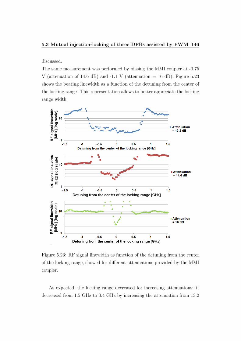
5.3 Mutual injection-locking of three DFBs assisted by FWM 146
discussed.
The same measurement was performed by biasing the MMI coupler at -0.75
V (attenuation of 14.6 dB) and -1.1 V (attenuation = 16 dB). Figure 5.23
shows the beating linewidth as a function of the detuning from the center of
the locking range. This representation allows to better appreciate the locking
range width.
Figure 5.23: RF signal linewidth as function of the detuning from the center
of the locking range, showed for different attenuations provided by the MMI
coupler.
As expected, the locking range decreased for increasing attenuations: it
decreased from 1.5 GHz to 0.4 GHz by increasing the attenuation from 13.2

5.3 Mutual injection-locking of three DFBs assisted by FWM 147
dB to 16 dB (consistently with Figure 5.20). Under unlocked conditions,
different mutual injection levels resulted in different values of the beating
linewidth. However, the most important result is the values of the RF signal
linewidth within the locking range. By extracting the data from the previ-
ous graphs, Figure 5.24 shows the minimum and the average values of the
linewidth of the RF signal measured within the locking range, plotted as
function of the optical attenuation.
Figure 5.24: Minimum and the average values of the RF signal linewidth as
function of the optical attenuation, measured within the locking range.
Once the locking was reached, the average RF signal linewidth was con-
stantly smaller than 5 MHz, independently from the levels of injection. More-
over, a minimum linewidth smaller than 3 MHz was always achievable in the
center of the locking range. This means that the injection levels can be
tuned in order to achieve a wide locking range without affecting the beating
linewidth.
This result gains particular interest when combined with the results showed
in the previous Section, regarding the beating linewidth with respect of the
locking frequency. When the locking occurs, the linewidth of the photomix-
ing signal is insensitive to both injection levels and the frequency at which
the locking occurs. The lasers are synchronised as a single oscillator, and
consequently the narrowing does not depends from any external factor such
as mutually injected power or frequency detuning between the lasers.

5.3 Mutual injection-locking of three DFBs assisted by FWM 148
5.3.6 High-frequency measurements
The final set of measurements focussed on the demonstration of the mu-
tual injection locking at higher detuning between the lasers, in order to gener-
ate RF signals at higher frequencies. The limited bandwidth of the spectrum
analyser allowed an exhaustive characterisation of the locking properties for
detuning between the lasers only up to 40 GHz. Since one of the advantages
of the photomixing technique is the easy and wide tunability of the gener-
ated RF signal up to hundreds of GHz, its improvement based on the mutual
injection locking is expected to fulfil the same duty.
In order to achieve the higher levels of injection necessary to lock the lasers
at hundreds of GHz of detuning, the device Design 3 was used. The aim of
the measurements was to asses the locking at 160 GHz (detuning of 1.28 nm)
and 280 GHz (2.24 nm), which correspond respectively to injection inside
and outside the stop-band of DFB-3.
The method used to verify whether the locking occurred was based on the
analysis of the optical spectrum of the collected signal. The lasers were bi-
ased close to the locking condition, then the current of one of the lasers was
tuned. When the injection levels were sufficiently high to allow the mutual
injection locking, a sharp jump of the lasing modes was visible. Due to
the high levels of injection, the FWM clones were powerful enough to pull
the lasing modes of DBF-1 and DFB-2, satisfying the locking condition and
therefore phase-locking them. During the locking range, explored by tuning
the current of one of the lasers, the lasing frequencies of the lasers were sta-
bly equally spaced. The locking was also verified by looking at the FWM
products on the side of the three lasers, which were collapsing into a single
peak during the locking range. Although this method cannot provide 100%
certainty about the occurrence of the locking, it represents a valid and sig-
nificative preliminary investigation of the locking properties for the largely
detuned lasers.
To demonstrate the locking at 160 GHz the device was biased as follow: DFB-
1 = 68.7 mA, DFB-2 = 148.8 mA, DFB-3 = 115.34 mA. The SOA/attenuators

5.3 Mutual injection-locking of three DFBs assisted by FWM 149
between the lasers 1-3 and 2-3 were biased respectively at -0.1 V and -0.4 V,
in order to adjust the levels of injection. DFB-1 current was swept between
68.7 and 69.7 mA to meet the locking condition. Figure 5.25 shows the map
of the optical spectrum of the collected signal. DFB-1-2-3 are visible as pow-
erful red peaks in the center of the map, while the less powerful light-blue
peaks are due to secondary FWM products generated in the laser cavities.
Figure 5.25: Map of the optical spectrum during the DFB-1 current tuning.
The two sharp jumps of the DFB-1 mode define the locking range.
In the bottom part of the map for DFB-1 currents up to 69 mA, also vis-
ible in the single spectra A, the three lasers were unlocked. Each DFB mode
is surrounded by FWM products. Even DFB-3, usually not superimposed by
any FWM clone, was nearly injected by FWM products. These modes were
generated as cascading of the FWM process between the lasers mode and the
main FWM products. Due to the high levels of injection, this cascaded FWM

5.3 Mutual injection-locking of three DFBs assisted by FWM 150
process created powerful modes on the side of DFB-1 and DFB-2. Since the
lasers were biased far from the locking condition, multiple FWM peaks are
visible. When DFB-1 was biased around 69 mA the locking occurred (Figure
5.25B). All the main FWM clones and DFB modes collapsed into single fre-
quency modes, as well as the cascaded FWM products. This situation was
stably maintained for around 0.5 mA (1.5 GHz). Then, the lasers unlocked.
The locking was confirmed by a optical linewidth measurement. Under un-
locked condition the optical linewidth of DFB-3, measured with the hetero-
dyne method, was 12.2 MHz. Then, once the locking occurred, the linewidth
narrowed at 9.8 MHz. This reduction (even if smaller than the ones pre-
viously measured) allow the assumption that the locking took place. The
smaller linewidth reduction might be due to the higher levels of optical power
injected into DFB-3, that tend to reduce the stability of the system. How-
ever, due to the very high frequency of the generated photomixing signal, the
linewidth and the phase noise of the RF signal could not be measured.
The same experiment was repeated also for detuning of 280 GHz. Such a
detuning value was important to assess the possibility to lock the lasers also
when the injection occurs outside the stop-band of the DFB-3, and there-
fore without taking advantage of the strong cavity effect which enhances the
power of the FWM clones.
DFB-1-2 of device Design 3 were respectively biased at currents of 60 mA
and 197.2 mA, while DFB-3 was swept from 141.5 to 142.5 mA to meet
the locking condition. The attenuators 1-3 and 3-2 were biased at -0.3 V
and -0.65 V to balance the mutual injection. Figure 5.26 shows the optical
spectrum map of the collected signal.
A locking process very similar to the one described for detuning of 160
GHz occurred. Although now the sweeping laser was DFB-3, the final effect
did not change. The strong mutual injection forced the lasers to jump in a
equally spaced configuration. At DFB-3 = 141.8 mA the small increase of
current corresponded to a red-jump of DFB-3 and a wider blue- jump of the
mode of DFB-1, although the current of latter was constant. The locking

5.3 Mutual injection-locking of three DFBs assisted by FWM 151
Figure 5.26: Map of the optical spectrum during the DFB-3 current tuning.
The locking took place for DFB-3 currents between 141.8 and 142.3 mA.
range lasted for around 0.5 mA, corresponding to 1.5 GHz, then the lasers
unlocked. Due to the larger mode jump experienced by DFB-1, the unlock-
ing of the lasers was more visible in this case when compared to that in
Figure 5.25. The optical linewidth measurements confirmed the same values
reported for the locking at 160 GHz, with a reduction of only few MHz, from
12.3 to 9.6 MHz.
As anticipated, the method used to investigate the locking at high frequen-
cies cannot ensure the certainty of the fact that the locking really occurred.
However, it shows that most probably it took place, and suggests further
investigations of this behaviour. A valid method to be used for further in-
vestigations is based on a interferometric technique capable to measure the
degree of phase correlation between two or more laser modes [97].

Conclusions
This thesis dealt with the design, fabrication and characterisation of
a Photonic Integrated Circuit for the generation of tunable and narrow-
linewidth mm-wave signals. Several optical components were successfully
integrated into a single monolithic device. By means of this device, the
newly proposed photomixing technique assisted by mutual injection lock-
ing and a non-linear Four Wave Mixing process was demonstrated, and the
phase-locking phenomenon of three different lasers was achieved and fully
characterised. The successfully integration was accomplished thanks to an
exhaustive design and careful fabrication of the devices, and important ex-
perimental results were obtained after a precise analysis of the complex dy-
namics of the devices.
The design of the basic building blocks which composed the different
devices was carried out with the goal of employing a fully post-growth fab-
rication process, capable to avoid the complex and expensive regrowth of
active optical material. Starting from the properties of the chosen InP-
based material, the waveguide design was conceived. It was based on a ridge
shallow-etched configuration, which ensured a reduced carrier recombination
rate (thus enhancing the lifetime of the device) and low sidewall roughness
(causing negligible optical back-reflections). An Al-containing layer, grown
on top of the core, was used as stop-etch layer for a reliable definition of
the ridge height of the different optical structures. The optimum waveguide

5.3 Mutual injection-locking of three DFBs assisted by FWM 153
geometry was determined based on the outcome of BPM simulations, with 2
µm width and a 1920 nm ridge height.
The design of the Bragg gratings for the DFB lasers was developed with a
view to the definition of the optimal value for the normalised grating cou-
pling coefficient κL. The optimal value was found to be κL = 3, and this
was successfully confirmed by experimental results. Phase-shifted gratings
were used to ensure a high yield of lasers exhibiting single mode operation
and precise and predictable lasing wavelength. In order to comply with the
constraints set by a fully post-growth fabrication process, side-etched grat-
ings were conceived and designed. They were defined by periodically varying
the waveguide width W and lateral recess d of the ridge waveguide. One of
the requirements for the different lasers that formed a single device was that
their nominal wavelength could be chosen precisely and independently. It
was concluded that the variation of the sole waveguide width W was prefer-
able, since it allowed a more predictable definition of the different optical
structures. Finally, evanescent field couplers and MultiMode Interference
couplers were designed.
The whole fabrication process of the devices, personally carried out in
the cleanrooms of the James Watt Nanofabrication Centre of the University
of Glasgow, U.K., was fully described. The main steps of the fabrication
process were analysed, with particular attention paid to the etching of the
material. It was shown that, by using an etching chemistry of CH4/H2/O2,
the Al-containing layer previously mentioned could be successfully used as a
stop-etch layer for a more precise definition of the optical structures. More-
over, the effects of the so-called RIE-lag were investigated. By means of test
samples, the range of values for lateral recess d of the Bragg grating that
ensures (for the employed technology process) the highest fabrication relia-
bility was found to be between 100 nm and 400 nm. Smaller recesses could
not be fabricated due to the non-ideal verticality ensured by the RIE etching

5.3 Mutual injection-locking of three DFBs assisted by FWM 154
process, while for larger recesses the under-etch due to the RIE-lag effect did
not allow the precise definition of the grating.
The characterisation of the devices started from the measurements of the
properties of the DFB lasers. The coupling coefficient κ and stop-band of
each laser were firstly determined. Then, by comparison with the values of
threshold current and SMSR, the effective optimal geometry of the gratings
was found. Moreover, the precision in defining the Bragg wavelength spacing
between different lasers was characterised. A three DFBs array was fabri-
cated, and the wavelength spacing between the lasers was precisely measured
below and above threshold. It was found that, with the employed design
and technology, a wavelength spacing of 0.16 nm, or 20 GHz, can be ob-
tained. It was done by varying only the geometrical characteristics of the
gratings, without changing any other operative parameter of the lasers. This
result proves that the developed technology allows the fabrication of multi-
wavelength laser arrays for DWDM applications (with a frequency spacing
of 25 GHz) using low-cost processing. Finally, the long term stability of the
fabricated DFB lasers was analysed, in order to check the stability of their
basic lasing characteristics, such as lasing wavelength and output power. It
was found that the lasing properties are stable and reliable over the time.
The locking experiments started from the characterisation of the mutual
injection locking of two DFBs operating at the same frequency. When the
optical mode of one of the lasers was superimposed to the other, the locking
occurred. Different locking regimes were found, depending on the amount of
the (electrically controlled) optical attenuation set between the lasers. For
attenuations smaller than 38 dB the locking was unstable, because too high
levels of optical injection drove the lasers into an unstable regime. Between
38 dB and 42 dB of optical attenuation, the two lasers were stably locked,
5.3 Mutual injection-locking of three DFBs assisted by FWM 155
and the expected dependence of the locking range on the mutual injected
power was found.
Since the technique of mutual injection locking assisted by FWM entails the
mutual injection of two lasers operating at distinct wavelengths via their
FWM clones, the efficiency in producing those FWM signals was charac-
terised. It was found that, depending on the geometry of the device, very
different efficiencies can be obtained. By using an above-threshold DFB laser
as FWM medium, the cavity enhancement effect allowed the efficient genera-
tion of FWM clones up to several hundreds of GHz. On the other hand, when
a simple SOA was used as FWM medium, the efficiency rapidly decreased
down to negligible values after a few GHz. These measurements, together
with the characterisation of the locking of two directly mutually injected
lasers, provided information about the practical values of optical attenuation
necessary to reach the stable locking of the lasers. Too high injection would
lead to an unstable locking regime, while too low level of injection would
prevent the occurrence of the mutual locking.
The locking experiments of three mutually injected DFBs followed. When
the DFBs were biased to meet the locking condition, the locking occurred.
Successfully locking could be achieved only by using the devices Design 1,
2, 3 (Figure 2.1), due to their higher efficiency in producing the FWM sig-
nals. By direct- or reverse-biasing the SOA/attenuators, each of those devices
showed good locking properties; however, due to the fact that the MMI cou-
pler of Design 2 could be used as additional SOA/attenuator, this device
was considered the best. No locking was reached with Design 4, mainly due
to the insufficient power of the generated FWM clones.
Upon locking condition, the RF signal obtained from the beating of the three
lasers on a high speed photodiode experienced a sharp narrowing of its elec-
trical linewidth. It narrowed from 47 MHz (unlocked case) down to 2.1 MHz
(locked case), showing a notable reduction by a factor 20. Three different
indicators were analysed in order to confirm the occurrence of the locking:
i) the occurrence of the collapse of two distinct RF beating signals into a

5.3 Mutual injection-locking of three DFBs assisted by FWM 156
single one, allowing to determine the locking range; ii) the optical linewidth
reduction of each laser; iii) the reduction of phase noise of the generated RF
signal.
It was also shown that, once the locking occurred, the frequency of the gener-
ated RF signal could be continuously tuned over a wide range of frequencies
by changing the frequency separation between the lasers in a simple manner,
i.e. by means of a tuning of their bias currents.
A stable locking was measured for RF beating frequencies in the range 5-40
GHz, and investigations based on the analysys of the optical spectrum of
the generated signals showed that the locking occurred also at 160 GHz and
280 GHz of separation between the lasers. The measured FWM efficiencies
allows the assumption that the mutual injection locking can be achieved up
to the THz range.
The locking properties were analysed with respect to the operating condi-
tion of the device. First of all, it was confirmed that, as in the case of two
mutually injected DFBs, the locking range for the three-lasers case decreases
for increased optical attenuations between the lasers. The linewidth of the
generated RF signal was characterised while varying the frequency separa-
tion between the lasers, yielding an average value of 2.5 MHz with small
deviations over the full range. The steadiness of the above measured values
suggested that, when the three lasers are mutually locked, the system oper-
ates as a single, complex and combined optical oscillator. Its optical output,
represented by the three optical signals, exhibited an excellent overall signal
stability (expressed by the linewidth of the RF signal). The stability of the
system is limited by some extrinsic factors (such as excess noise of the driv-
ing current sources and residual temperature fluctuations) and some intrinsic
effects (such as the intrinsic phase noise limit) caused by carrier fluctuations
and the linewidth enhancement factor).
The linewidth of the generated RF signal was characterised also with respect
to the levels of mutually injected power. It was shown that, once the locking
condition was satisfied, the average RF signal linewidth was constantly able

5.3 Mutual injection-locking of three DFBs assisted by FWM 157
to reach a minimum value smaller 3 MHz, independently from the injection
levels. These results allowed to draw the important conclusion that, when
the locking occurs, the linewidth of the RF generating signal is insensitive
to both injection levels and the frequency at which the locking occurs. This
favours the interpretation that when the lasers are synchronised the system
acts as a single compound oscillator. The value of the linewidth of the beating
signals (which expresses the degree of mutual phase correlation between the
individual lasers) is independent from any external factor, such as mutually
injected power or frequency detuning between the lasers.
Final remarks of the Cariplo Project 2007-5263
As final remarks, some strengths and weaknesses of the Project 2007-5263
”Semiconductor lasers with nanostructured gratings for wireless application
signal generation” can be highlighted.
Strengths
• The development path from the encouraging results obtained with the
first experimental setup constituted by discrete optical components, to
the full integration into a single monolithic optoelectronic device has
been successfully completed. The mutual injection locking has been
demonstrated and its properties have characterised for frequencies up
to 40 GHz. This aspect represents an important plus for the monolithic
integration of complex optoelectronic devices.
• The mutual injection locking of three DFB lasers operating at different
frequencies and integrated onto a single monolithic device has been
successfully demonstrated for the first time.
• The device can be interpreted as an optoelectronic super-oscillator,
where the three single optical oscillators (i.e. the DFB lasers) can be

5.3 Mutual injection-locking of three DFBs assisted by FWM 158
phase-locked via an all-optical synchronisation process. Future theoret-
ical analysis may help towards a deeper comprehension of the intrinsic
locking mechanism, and to the unveil of new applications.
• The fabricated devices can be used to theoretically and practically
study complex phenomena such as injection locking and coupled os-
cillators systems. The devices can be also used to validate theoretical
models normally applied in more complex coupled systems, such as for
network synchronisation and neurological applications.
Weaknesses
• The measured reduction of the linewidth of the generated RF signal
is considerable, but it may be not enough for applications that require
high levels of spectral purity, such as local oscillator for telecommuni-
cations and radioastronomy.
• The output of the fabricated devices provides an optical signal, and an
external high speed photodetector is still necessary in order to generate
the electrical RF signal.
• The experiments showed promising results with a future perspective of
extension to the THz range. However, the upper frequency limit and
the properties of the generated signal at high frequencies are still to be
characterised.
• An exhaustive theoretical model of the devices and the locking mech-
anism is needed. The limited funding and promising results obtained
from the discrete components setup led to the prioritisation of the ex-
perimental approach.
5.3 Mutual injection-locking of three DFBs assisted by FWM 159
Future work
In this work, the complex experimental setup composed by discrete opti-
cal components was successfully integrated into a single Photonic Integrated
Device, which functionality for the generation of RF signal was fully charac-
terised. As future works, a slight modification of the devices is advised. A
reduced optical linewidth of each oscillator (i.e. the DFB lasers) in unlocked
condition may improve the overall stability of the system once the locking
occurs. Moreover, longer and multi contact SOA/attenuators would allow a
better control of the injection levels. An hybrid integration of fabricated de-
vices with photomixers or the full integration of a Low Temperature Grown
(LTG) photomixer onto same substrate may improve the compactness of the
photomixing system. Finally, the devices should be tested on-the-field, as
integrated sources for THz-related applications. Even if the linewidth under
locking condition still lies in the MHz scale, the integrated devices would
represent an interesting alternative to the commercially available bulky THz
sources, currently offered by Picometrix, TeraView and Toptica.

Bibliography
[1] N. Gibbons, M. Soldo, and G. Giuliani, “Generation of a narrow
linewidth mm-wave signal from two phase-locked DFB lasers that are
mutually coupled via four wave mixing,” in Lasers and Electro-Optics
2009 and the European Quantum Electronics Conference. CLEO Europe
- EQEC 2009. European Conference on, p. 1, june 2009.
[2] S. Singh, F. Ziliotto, U. Madhow, E. Belding, and M. Rodwell, “Blockage
and directivity in 60 GHz wireless personal area networks,” IEEE J.Sel.
A. Commun., vol. 27, pp. 1400–1413, October 2009.
[3] R. Abou Jaoude, “ACC radar sensor technology test requirements and
test solutions,” Intelligent Transportation Systems, IEEE Transactions
on, vol. 4, pp. 115 – 122, Sept 2003.
[4] J. Payne, B. Shillue, and A. Vaccari, “Photonic techniques for use on
the Atacama Large Millimeter Array,” in Microwave Photonics, 1999.
MWP ’99. International Topical Meeting on, pp. 105 –108 vol.1, 1999.
[5] H. Lin, W. Withayachumnankul, B. Fischer, S. Mickan, and D. Ab-
bott, “Gas recognition with terahertz time-domain spectroscopy and
reference-free spectrum: A preliminary study,” in Infrared, Millime-
ter and Terahertz Waves, 2008. IRMMW-THz 2008. 33rd International
Conference on, pp. 1 –2, sept. 2008.
[6] D. Mittleman, R. Jacobsen, R. Neelamani, R. Baraniuk, and
M. Nuss, “Gas sensing using terahertz time-domain spectroscopy,”
BIBLIOGRAPHY 161
Applied Physics B: Lasers and Optics, vol. 67, pp. 379–390, 1998.
10.1007/s003400050520.
[7] H. Sun, Y. Ding, and I. Zotova, “THz Spectroscopy by Frequency-
Tuning Monochromatic THz Source: From Single Species to Gas Mix-
tures,” Sensors Journal, IEEE, vol. 10, pp. 621 –629, march 2010.
[8] X.-C. Zhang, “Three-dimensional terahertz wave imaging,” Philosophi-
cal Transactions of the Royal Society of London. Series A: Mathemati-
cal, Physical and Engineering Sciences, vol. 362, no. 1815, pp. 283–299,
2004.
[9] D. M. Mittleman, S. Hunsche, L. Boivin, and M. C. Nuss, “T-ray to-
mography,” Opt. Lett., vol. 22, pp. 904–906, Jun 1997.
[10] T. Yasuda, T. Yasui, T. Araki, and E. Abraham, “Real-time two-
dimensional terahertz tomography of moving objects,” Optics Commu-
nications, vol. 267, no. 1, pp. 128 – 136, 2006.
[11] D. Creeden, J. C. McCarthy, P. A. Ketteridge, P. G. Schunemann,
T. Southward, J. J. Komiak, and E. P. Chicklis, “Compact, high av-
erage power, fiber-pumped terahertz source for active real-time imaging
of concealed objects,” Opt. Express, vol. 15, pp. 6478–6483, May 2007.
[12] H.-B. Liu, H. Zhong, N. Karpowicz, Y. Chen, and X.-C. Zhang, “Tera-
hertz Spectroscopy and Imaging for Defense and Security Applications,”
Proceedings of the IEEE, vol. 95, pp. 1514 –1527, aug. 2007.
[13] K. Yamamoto, M. Yamaguchi, F. Miyamaru, M. Tani, M. Hangyo,
T. Ikeda, A. Matsushita, K. Koide, M. Tatsuno, and Y. Minami, “Nonin-
vasive Inspection of C-4 Explosive in Mails by Terahertz Time-Domain
Spectroscopy,” Japanese Journal of Applied Physics, vol. 43, no. 3B,
pp. L414–L417, 2004.
BIBLIOGRAPHY 162
[14] H. Zhong, J. Xu, X. Xie, T. Yuan, R. Reightler, E. Madaras, and X.-
C. Zhang, “Nondestructive defect identification with terahertz time-of-
flight tomography,” Sensors Journal, IEEE, vol. 5, pp. 203 – 208, april
2005.
[15] K. Kawase, “Terahertz Imaging For Drug Detection And Large-Scale
Integrated Circuit Inspection,” Opt. Photon. News, vol. 15, pp. 34–39,
Oct 2004.
[16] L. Ohrstrom, A. Bitzer, M. Walther, and F. J. Ruhli, “Technical note:
Terahertz imaging of ancient mummies and bone,” American Journal of
Physical Anthropology, vol. 142, no. 3, pp. 497–500, 2010.
[17] K. Fukunaga, Y. Ogawa, S. Hayashi, and I. Hosako, “Terahertz imaging
for analysis of historic paintings and manuscripts,” in Infrared, Millime-
ter and Terahertz Waves, 2008. IRMMW-THz 2008. 33rd International
Conference on, pp. 1 –3, sept. 2008.
[18] M. Mukherjee, N. Mazumder, S. K. Roy, and K. Goswami, “GaN IM-
PATT diode: a photo-sensitive high power terahertz source,” Semicon-
ductor Science and Technology, vol. 22, no. 12, p. 1258, 2007.
[19] E. Alekseev and D. Pavlidis, “GaN Gunn diodes for THz signal gener-
ation,” in Microwave Symposium Digest., 2000 IEEE MTT-S Interna-
tional, vol. 3, pp. 1905 –1908 vol.3, 2000.
[20] A. Raisanen, “Frequency multipliers for millimeter and submillimeter
wavelengths ,” Proceedings of the IEEE, vol. 80, pp. 1842 –1852, nov
1992.
[21] E. Seok, C. Cao, D. Shim, D. Arenas, D. Tanner, C.-M. Hung, and
K. O, “A 410GHz CMOS Push-Push Oscillator with an On-Chip Patch
Antenna,” in Solid-State Circuits Conference, 2008. ISSCC 2008. Digest
of Technical Papers. IEEE International, pp. 472 –629, feb. 2008.

BIBLIOGRAPHY 163
[22] M. Dyakonov and M. Shur, “Plasma wave electronics: novel terahertz
devices using two dimensional electron fluid,” Electron Devices, IEEE
Transactions on, vol. 43, pp. 1640 –1645, oct 1996.
[23] T. Nagatsuma, A. Hirata, N. Shimizu, H.-J. Song, and N. Kukutsu,
“Photonic generation of millimeter and terahertz waves and its appli-
cations,” in Applied Electromagnetics and Communications, 2007. ICE-
Com 2007. 19th International Conference on, pp. 1 –4, sept. 2007.
[24] A. Stohr and D. Jdger, “Photonic Millimeter-wave and Terahertz Source
Technologies (invited paper),” in Microwave Photonics, 2006. MWP ’06.
International Topical Meeting on, pp. 1 –4, oct. 2006.
[25] I. Kim and K. Lau, “Frequency and timing stability of mode-locked semi-
conductor lasers-passive and active mode locking up to millimeter wave
frequencies,” Quantum Electronics, IEEE Journal of, vol. 29, pp. 1081
–1090, apr 1993.
[26] R. Koumans and R. Van Roijen, “Theory for passive mode-locking in
semiconductor laser structures including the effects of self-phase mod-
ulation, dispersion, and pulse collisions,” Quantum Electronics, IEEE
Journal of, vol. 32, pp. 478 –492, mar 1996.
[27] S. Kim, H.-C. Ryu, S. Kang, S. Y. Jeong, S. Lee, D. Kang, M. Kwak,
S. K. Choi, M. C. Paek, and K.-Y. Kang, “The first experimental results
of mm-wave generation by photomixing,” in Infrared, Millimeter and
Terahertz Waves, 2008. IRMMW-THz 2008. 33rd International Con-
ference on, pp. 1 –2, sept. 2008.
[28] H. Pahlevaninezhad, B. Heshmat, and T. Darcie, “Modeling terahertz
heterodyne detection based on photomixing,” in Radar Conference, 2010
IEEE, pp. 113 –116, may 2010.
[29] E. Brown, “THz Photomixing,” in Lasers and Electro-Optics Society,

BIBLIOGRAPHY 164
2007. LEOS 2007. The 20th Annual Meeting of the IEEE, pp. 790 –791,
oct. 2007.
[30] R. Ramos and A. Seeds, “Fast heterodyne optical phase-lock loop using
double quantum well laser diodes,” Electronics Letters, vol. 28, pp. 82
–83, jan. 1992.
[31] A. Bordonalli, C. Walton, and A. Seeds, “High-performance phase lock-
ing of wide linewidth semiconductor lasers by combined use of optical
injection locking and optical phase-lock loop,” Lightwave Technology,
Journal of, vol. 17, pp. 328 –342, feb 1999.
[32] L. Langley, M. Elkin, C. Edge, M. Wale, U. Gliese, X. Huang, and
A. Seeds, “Packaged semiconductor laser optical phase-locked loop
(OPLL) for photonic generation, processing and transmission of mi-
crowave signals,” Microwave Theory and Techniques, IEEE Transac-
tions on, vol. 47, pp. 1257 –1264, jul 1999.
[33] L. Goldberg, H. Taylor, J. Weller, and D. Bloom, “Microwave signal gen-
eration with injection-locked laser diodes,” Electronics Letters, vol. 19,
pp. 491 –493, 23 1983.
[34] L. Goldberg, A. Yurek, H. Taylor, and J. Weller, “35 GHz microwave sig-
nal generation with an injection-locked laser diode,” Electronics Letters,
vol. 21, pp. 814 –815, 29 1985.
[35] Y. J. Wen, H. F. Liu, D. Novak, and Y. Ogawa, “Millimeter-wave signal
generation from a monolithic semiconductor laser via subharmonic op-
tical injection,” Photonics Technology Letters, IEEE, vol. 12, pp. 1058
–1060, aug 2000.
[36] R. Goto, T. Goto, H. Kasuya, M. Mori, and K. Yamane, “Mutual injec-
tion locking between two DFB LDs which lase at frequencies separated
by one Fabry-Perot mode spacing,” Electronics Letters, vol. 34, pp. 1669
–1670, aug 1998.

BIBLIOGRAPHY 165
[37] G. P. Agrawal, “Population pulsations and nondegenerate four-wave
mixing in semiconductor lasers and amplifiers,” J. Opt. Soc. Am. B,
vol. 5, pp. 147–159, Jan 1988.
[38] T. Higashi, S. Sweeney, A. Phillips, A. Adams, E. O’Reilly, T. Uchida,
and T. Fujii, “Observation of reduced nonradiative current in 1.3 µm
AlGaInAs-InP strained MQW lasers,” Photonics Technology Letters,
IEEE, vol. 11, pp. 409 –411, apr 1999.
[39] Y.-K. Kuo, S.-H. Yen, M.-W. Yao, M.-L. Chen, and B.-T. Liou, “Nu-
merical study on gain and optical properties of AlGaInAs, InGaNAs,
and InGaAsP material systems for 1.3 µm semiconductor lasers,” Op-
tics Communications, vol. 275, no. 1, pp. 156 – 164, 2007.
[40] M. Camargo Silva, J. Sih, T. Chou, J. Kirk, G. Evans, and J. Butler,
“1.3 µm strained MQW AlGaInAs and InGaAsP ridge-waveguide lasers
- a comparative study,” in Microwave and Optoelectronics Conference,
1999. SBMO/IEEE MTT-S, APS and LEOS - IMOC ’99. International,
vol. 1, pp. 10 –12 vol. 1, 1999.
[41] A. Kasukawa, R. Bhat, C. Zah, S. Schwarz, D. Hwang, M. Koza,
and T. Lee, “Low threshold current density 1.5 µm GaInAs/AlGaInAs
graded-index separate-confinement-heterostructure quantum well laser
diodes grown by metal organic chemical vapour deposition,” Electronics
Letters, vol. 27, pp. 1063 –1065, june 1991.
[42] M. Guden and J. Piprek, “Material parameters of quaternary III - V
semiconductors for multilayer mirrors at 1.55 µm wavelength,” Mod-
elling and Simulation in Materials Science and Engineering, vol. 4, no. 4,
p. 349, 1996.
[43] S. Furst, Monolithic Integration of Semiconductor Ring Lasers. PhD
thesis, University of Glasgow, 2008.

BIBLIOGRAPHY 166
[44] G. Mezosi, Semiconductor Ring Lasers for all-optical signal processing.
PhD thesis, University of Glasgow, 2010.
[45] D. Marcuse, “Reflection loss of laser mode from tilted end mirror,” Light-
wave Technology, Journal of, vol. 7, pp. 336 –339, feb 1989.
[46] W. Bragg, “The Diffraction of Short Electromagnetic Waves by a
Cristal,” Proceedings of Cambridge Philosophical Society, 1913.
[47] H. Kogelnik and C. V. Shank, “Coupled-Wave Theory of Distributed
Feedback Lasers,” vol. 43, no. 5, pp. 2327–2335, 1972.
[48] J. Buus, M. Amann, and D. Blumenthal, Tunable laser diodes and re-
lated optical sources. SPIE PM, Wiley-Interscience, 2005.
[49] H. Ghafouri-Shiraz and B. Lo, Distributed feedback laser diodes: princi-
ples and physical modelling. Wiley, 1996.
[50] L. Coldren and S. Corzine, Diode lasers and photonic integrated circuits.
Wiley series in microwave and optical engineering, Wiley, 1995.
[51] J. Carroll, J. Whiteaway, and D. Plumb, Distributed feedback semicon-
ductor lasers. IEE circuits, devices and systems series, Institution of
Electrical Engineers, 1998.
[52] S. Chinn, “Effects of mirror reflectivity in a distributed-feedback laser,”
Quantum Electronics, IEEE Journal of, vol. 9, pp. 574 – 580, jun 1973.
[53] C. A. Ferreira Fernandes, “Single-mode yield in dfb laser diodes with
reflecting facets,” Microwave and Optical Technology Letters, vol. 48,
no. 2, pp. 205–209, 2006.
[54] H. Haus and C. Shank, “Antisymmetric taper of distributed feedback
lasers,” Quantum Electronics, IEEE Journal of, vol. 12, pp. 532 – 539,
sep 1976.
BIBLIOGRAPHY 167
[55] K. Utaka, S. Akiba, K. Sakai, and Y. Matsushima, “Analysis of quarter-
wave-shifted DFB laser,” Electronics Letters, vol. 20, pp. 326 –327, 12
1984.
[56] M. Okai, S. Tsuji, and N. Chinone, “Stability of the longitudinal mode
in λ/4-shifted InGaAsP/InP DFB lasers,” Quantum Electronics, IEEE
Journal of, vol. 25, pp. 1314 –1319, jun 1989.
[57] L. Miller, J. Verdeyen, J. Coleman, R. Bryan, J. Alwan, K. Beernink,
J. Hughes, and T. Cockerill, “A distributed feedback ridge waveg-
uide quantum well heterostructure laser,” Photonics Technology Letters,
IEEE, vol. 3, pp. 6 –8, jan 1991.
[58] M. Zanola, M. Strain, M. Sorel, and G. Giuliani, “Post-Growth Fabri-
cation of a DFB Laser Array with High Side Mode Suppression Ratio
for DWDM Applications,” in European Semiconductor Laser Workshop
2011, Pavia, Italy, Sept 2010.
[59] M. Zanola, M. Strain, M. Sorel, and G. Giuliani, “Post-Growth Fabrica-
tion of a DFB Laser Array with High Precision Wavelength Spacing,” in
CLEO/Europe and EQEC 2011 Conference Digest, pp. CB11–1, Optical
Society of America, 2011.
[60] B. Saleh and M. Teich, Fundamentals of photonics. Wiley series in pure
and applied optics, Wiley-Interscience, 2007.
[61] H.-B. Lin, R.-S. Cheng, and W.-S. Wang, “Wide-angle low-loss single-
mode symmetric Y-junctions,” Photonics Technology Letters, IEEE,
vol. 6, pp. 825 –827, jul 1994.
[62] L. Soldano and E. Pennings, “Optical multi-mode interference devices
based on self-imaging: principles and applications,” Lightwave Technol-
ogy, Journal of, vol. 13, pp. 615 –627, apr 1995.
[63] O. Bryngdahl, “Image formation using self-imaging techniques,” J. Opt.
Soc. Am., vol. 63, pp. 416–419, Apr 1973.

BIBLIOGRAPHY 168
[64] P. Besse, M. Bachmann, H. Melchior, L. Soldano, and M. Smit, “Op-
tical bandwidth and fabrication tolerances of multimode interference
couplers,” Lightwave Technology, Journal of, vol. 12, pp. 1004 –1009,
jun 1994.
[65] A. Ferreras, F. Rodriguez, E. Gomez-Salas, J. de Miguel, and
F. Hernandez-Gil, “Useful formulas for multimode interference power
splitter/combiner design,” Photonics Technology Letters, IEEE, vol. 5,
pp. 1224 –1227, oct 1993.
[66] L. Soldano, F. Veerman, M. Smit, B. Verbeek, A. Dubost, and E. Pen-
nings, “Planar monomode optical couplers based on multimode interfer-
ence effects,” Lightwave Technology, Journal of, vol. 10, pp. 1843 –1850,
dec 1992.
[67] E. Pennings, R. van Roijen, M. van Stralen, P. de Waard, R. Koumans,
and B. Verbeck, “Reflection properties of multimode interference de-
vices,” Photonics Technology Letters, IEEE, vol. 6, pp. 715 –718, jun
1994.
[68] R. Hanfoug, L. M. Augustin, Y. Barbarin, J. J. G. M. van der Tol, E. A.
J. M. Bente, F. Karouta, D. Rogers, S. Cole, Y. S. Oei, X. J. M. Lei-
jtens, and M. K. Smit, “Reduced reflections from multimode interference
couplers,” Electronics Letters, vol. 42, 2006.
[69] H. Namatsu, T. Yamaguchi, M. Nagase, K. Yamazaki, and K. Kuri-
hara, “Nano-patterning of a Hydrogen SilsesQuioxane resist with re-
duced linewidth fluctuations,” Microelectronic Engineering, vol. 41-42,
pp. 331 – 334, 1998. International Conference on Micro- and Nanofar-
bication.
[70] G. T. Edwards, A. Sobiesierski, D. I. Westwood, and P. M. Smow-
ton, “Fabrication of high-aspect-ratio, sub-micron gratings in Al-
GaInP/GaAs laser structures using a BCl3/Cl2/Ar inductively coupled

BIBLIOGRAPHY 169
plasma,” Semiconductor Science and Technology, vol. 22, no. 9, p. 1010,
2007.
[71] L. Chee-Wei and C. Mee-Koy, “Room-Temperature Inductively Coupled
Plasma Etching of InP Using Cl2/N2 and Cl2/CH4/H2,” Chinese Physics
Letters, vol. 23, no. 4, p. 903, 2006.
[72] K. Kennedy, K. M. Groom, and R. A. Hogg, “Fabrication of v-groove
gratings in InP by inductively coupled plasma etching with SiCl4/Ar,”
Semiconductor Science and Technology, vol. 21, no. 1, p. L1, 2006.
[73] P. Strasser, R. Wuest, F. Robin, K. Rauscher, B. Wild, D. Erni, and
H. Jackel, “An ICP-RIE etching process for InP-based photonic crystals
using Cl2/Ar/N2 chemistry,” in Indium Phosphide and Related Materi-
als, 2005. International Conference on, pp. 242 – 245, may 2005.
[74] R. Grover, J. V. Hryniewicz, O. S. King, and V. Van, “Process devel-
opment of methane-hydrogen-argon-based deep dry etching of InP for
high aspect-ratio structures with vertical facet-quality sidewalls,” Jour-
nal of Vacuum Science Technology B: Microelectronics and Nanometer
Structures, vol. 19, pp. 1694 –1698, sep 2001.
[75] K. Shinoda, K. Nakahara, and H. Uchiyama, “InGaAlAs/InP
ridge-waveguide lasers fabricated by highly selective dry etching in
CH4/H2/O2 plasma,” in Indium Phosphide and Related Materials, 2003.
International Conference on, pp. 550 – 553, may 2003.
[76] T. R. Hayes, M. A. Dreisbach, P. M. Thomas, Dautremont, W. C. Smith,
and L. A. Heimbrook, “Reactive ion etching of InP using CH4/H2 mix-
tures: Mechanisms of etching and anisotropy,” Journal of Vacuum Sci-
ence Technology B: Microelectronics and Nanometer Structures, vol. 7,
pp. 1130 –1140, sep 1989.
[77] J. E. Schramm, D. I. Babic, E. L. Hu, J. E. Bowers, and J. L. Merz,
“Fabrication of high-aspect-ratio InP-based vertical-cavity laser mirrors
BIBLIOGRAPHY 170
using CH4/H2/O2/Ar reactive ion etching,” Journal of Vacuum Sci-
ence Technology B: Microelectronics and Nanometer Structures, vol. 15,
pp. 2031 –2036, nov 1997.
[78] M. Aoki, M. Komori, A. Taike, R. Yamabi, and K. Uomi, “Low-power-
consumption thin-film heater-loaded wavelength-tunable DFB laser,” in
Communications, 1999. APCC/OECC ’99. Fifth Asia-Pacific Confer-
ence on ... and Fourth Optoelectronics and Communications Conference,
vol. 2, pp. 1548 –1549 vol.2, 1999.
[79] C. Henry, “Theory of the linewidth of semiconductor lasers,” Quantum
Electronics, IEEE Journal of, vol. 18, pp. 259 – 264, feb 1982.
[80] R. Hui and M. O’Sullivan, Fiber optic measurement techniques. Else-
vier/Academic Press, 2009.
[81] D. Derickson, Fiber optic test and measurement. Hewlett-Packard pro-
fessional books, Prentice Hall PTR, 1998.
[82] A. L. Schawlow and C. H. Townes, “Infrared and Optical Masers,” Phys.
Rev., vol. 112, pp. 1940–1949, Dec 1958.
[83] H. Soda, Y. Kotaki, H. Sudo, H. Ishikawa, S. Yamakoshi, and H. Imai,
“Stability in single longitudinal mode operation in GaInAsP/InP phase-
adjusted DFB lasers,” Quantum Electronics, IEEE Journal of, vol. 23,
pp. 804 – 814, jun 1987.
[84] K. Kikuchi and H. Tomofuji, “Performance analysis of separated-
electrode DFB laser diode,” Electronics Letters, vol. 25, pp. 162 –163,
jan. 1989.
[85] T. Kimura and Sugimura, “Narrow linewidth asymmetric coupled phase-
shift DFB lasers,” Trans. IEICE, 1990.

BIBLIOGRAPHY 171
[86] D. Baney, B. Szafraniec, and A. Motamedi, “Coherent optical spectrum
analyzer,” Photonics Technology Letters, IEEE, vol. 14, pp. 355 –357,
mar 2002.
[87] B. Szafraniec, J. Y. Law, and D. M. Baney, “Frequency resolution and
amplitude accuracy of the coherent optical spectrum analyzer with a
swept local oscillator,” Opt. Lett., vol. 27, pp. 1896–1898, Nov 2002.
[88] R. Lang, “Injection locking properties of a semiconductor laser,” Quan-
tum Electronics, IEEE Journal of, vol. 18, pp. 976 – 983, jun 1982.
[89] S. Kobayashi and T. Kimura, “Injection locking characteristics of an
AlGaAs semiconductor laser,” Quantum Electronics, IEEE Journal of,
vol. 16, pp. 915 – 917, sep 1980.
[90] R. Hui, A. D’Ottavi, A. Mecozzi, and P. Spano, “Injection locking in
distributed feedback semiconductor lasers,” Quantum Electronics, IEEE
Journal of, vol. 27, pp. 1688 –1695, jun 1991.
[91] V. Annovazzi-Lodi, A. Scire, M. Sorel, and S. Donati, “Dynamic be-
havior and locking of a semiconductor laser subjected to external injec-
tion,” Quantum Electronics, IEEE Journal of, vol. 34, pp. 2350 –2357,
dec 1998.
[92] S. Noda, K. Kojima, and K. Kyuma, “Mutual injection-locking prop-
erties of monolithically-integrated surface-emitting multiple-quantum-
well distributed feedback lasers,” Quantum Electronics, IEEE Journal
of, vol. 26, pp. 1883 –1894, nov 1990.
[93] B. W. Hakki and T. L. Paoli, “Gain spectra in GaAs double-
heterostructure injection lasers,” Journal of Applied Physics, vol. 46,
pp. 1299 –1306, mar 1975.
[94] J. Minch, C.-S. Chang, and S.-L. Chuang, “Wavelength conversion in
distributed-feedback lasers,” Selected Topics in Quantum Electronics,
IEEE Journal of, vol. 3, pp. 569 –576, apr 1997.

BIBLIOGRAPHY 172
[95] E. Rubiola, Phase Noise and Frequency Stability in Oscillators. The
Cambridge RF and Microwave Engineering Series, Cambridge University
Press, 2010.
[96] I. Rosu, “Phase Noise in Oscillators,” tech. rep.,
http://www.qsl.net/va3iul/.
[97] M. Simonetta, M. Soldo, M. Zanola, M. Strain, M. Sorel, and G. Giu-
liani, “Measurement of phase-correlation between optical modes of Semi-
conductor Lasers,” in Lasers and Electro-Optics Europe (CLEO EU-
ROPE/EQEC), 2011 Conference on and 12th European Quantum Elec-
tronics Conference, p. 1, may 2011.

Acknowledgements
I would like to thank my advisers Prof. Guido Giuliani, Dr. Marc Sorel
and Dr. Michael J. Strain. You all gave me the opportunity to join a very
exciting research project, giving me invaluable help and guidance. This work
would have not been possible without your support and encouragement. Each
conversation with you was full of amazingly helpful guidelines, that allowed
me to reach the results reported in this work. By giving me the opportunity
to join the optogroup of the University of Glasgow, you let me live some of
the most incredible time of my life, under several scientific and less-scientific
aspects.
I ringraziamenti alla mia famiglia non potranno mai essere abbastanza. Mi
hanno sempre supportato in ogni mia scelta, anche le piu difficili per loro.
Mamma, questa tesi e dedicata a te perche so che per una mamma e difficile
stare lontano dal ”suo bambino”, piu che per nessun altro. Vedila dal lato
positivo: alloggio facile nella tua amata Scozia! Papi, grazie per aver suppor-
tato le mie scelte cosı tanto, ogni giorno capisco quanto tu sia fiero di me. E’
davvero importante, grazie. Luca, mentre scrivo sei alla tua prima notte in
collegio. Per me e stata un’esperienza incredibile, che ha mi ha fatto crescere
tantissimo. Ti auguro valga lo stesso anche per te, in bocca al lupo!!! Nonni
e nonna, ogni volta che torno a casa e un piacere incredibile vedervi cosı in
forma. Mi manca la vostra saggezza, siete sempre fonte di ispirazione per
me. Zii e Simone, io ve la butto lı... viaggetto in Scozia?? certo, forse le
stelle son difficili da vedere, ma di materiale per foto ce n’e alla grande, e
l’apple store ha prezzi abbastanza competitivi in questo periodo..

BIBLIOGRAPHY 174
And now it’s the moment for my lovely flatmate Kasia (ehehe I won’t give
you a point so easily!!). Since when I got to know you, a funky 70’s night
some time ago, my life changed. And I didn’t know it could be so cool. And
yellow. Thanks baby, you are really cool.. and special.. and for the rest...
well.. you know.. Supa!!
During these years I had the opportunity to work and chill out with amazing
people. Gabor, your knowledge about every scientific thing is overtaken only
about the number of beers you can drink. You taught me everything about
fabrication, thanks!! Piotr, your advices and help are simply great, and the
time we spend together inside and outside the lab is always very funny!! and
speaking about beers.. well.. what said above is true also for you! Guys, I
think nobody has ever seen me so angry like after the Richard P. joke: you
hold a record!! A big thanks also to Steven, your advices helped me a lot!!
A very special thank goes to Vincenzo, Piero e Felice. Vince, we met again
after the university, and I have to say I’m very happy that this happened.
Each conversation with you, scientific and not, is great and funny. And your
patience in explaining me even the most simple stuff is astonishing... Piero,
you are the first guy I met when I arrived in Glasgow. I really miss you, it
was so cool being clandestine with you! and btw, you should stop leaving
every few months!! Felice (i.e. Vecchio), the time we spent together cannot
be described. Especially in the end of a PhD thesis. So, as Mr. Wolf says,
let’s not start s.... A couple of words also to Irene, between the Glasgow and
Pavia people, for obvious reasons. I’m happy I convinced you to come up
north for a while, I’m sure you strongly needed it. But now, come and grab
your f** suitcases!
A big thanks also to Valeria and Enrico: recently we didn’t meet so often
(mostly for my fault I have to say..), but every time we met it was just
amazing! The final, special and leso thank goes to the Lazy Pavazy. Rossi,
Fu, Piaru, Mauri, Bea, Toma, Ardo: I missed you guys, a lot, but I’m sure
our zingarate will continue for long time to go!!! As tradition wants, I close
thanking ”i due bifolchi”, their ”solchi”, event and exclamation!!!


