Trends in High Speed Digital Interface Standards with Simulation and Measurement Perspectives
高速数字设计仿真测量的需求与发展趋向
May 21, 2015
Page
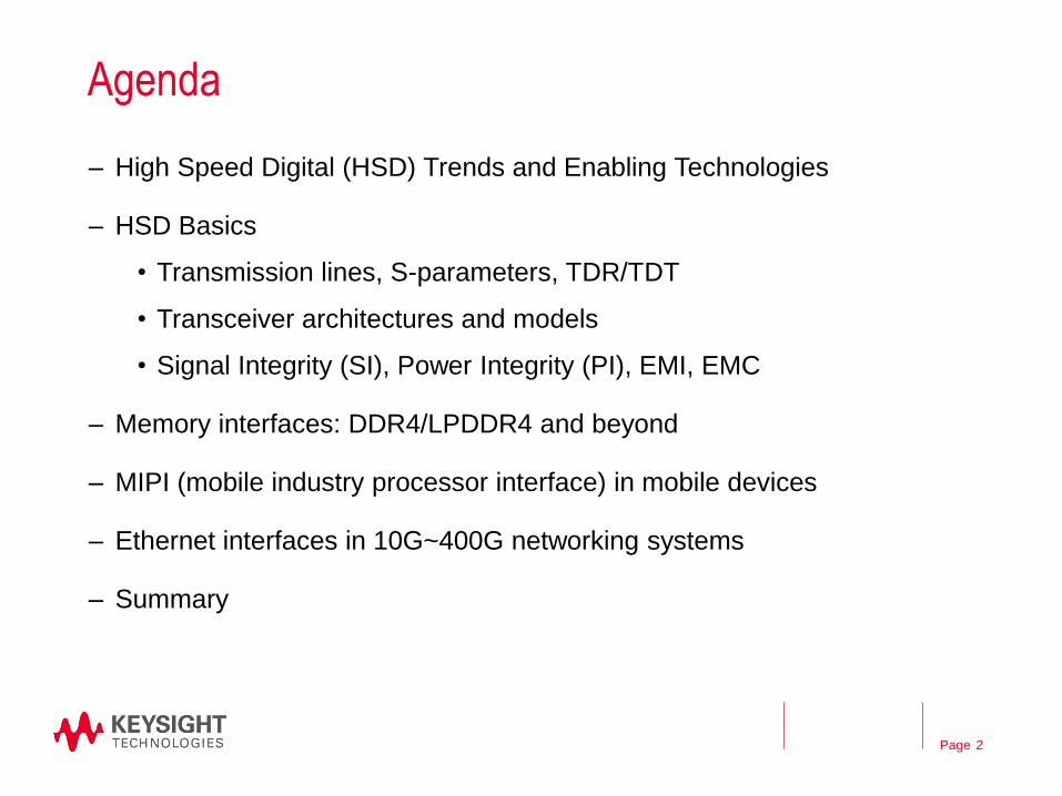
Agenda
– High Speed Digital (HSD) Trends and Enabling Technologies
– HSD Basics
• Transmission lines, S-parameters, TDR/TDT
• Transceiver architectures and models
• Signal Integrity (SI), Power Integrity (PI), EMI, EMC
– Memory interfaces: DDR4/LPDDR4 and beyond
– MIPI (mobile industry processor interface) in mobile devices
– Ethernet interfaces in 10G~400G networking systems
– Summary
2
Page 3
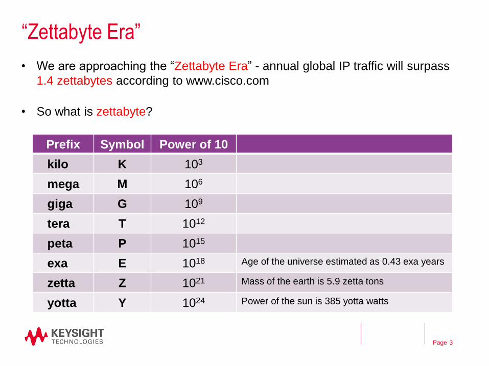
“Zettabyte Era”
• We are approaching the “Zettabyte Era” - annual global IP traffic will surpass
1.4 zettabytes according to www.cisco.com
• So what is zettabyte?
Prefix Symbol Power of 10
kilo K 103
mega M 106
giga G 109
tera T 1012
peta P 1015
exa E 1018 Age of the universe estimated as 0.43 exa years
zetta Z 1021 Mass of the earth is 5.9 zetta tons
yotta Y 1024 Power of the sun is 385 yotta watts
Page 4
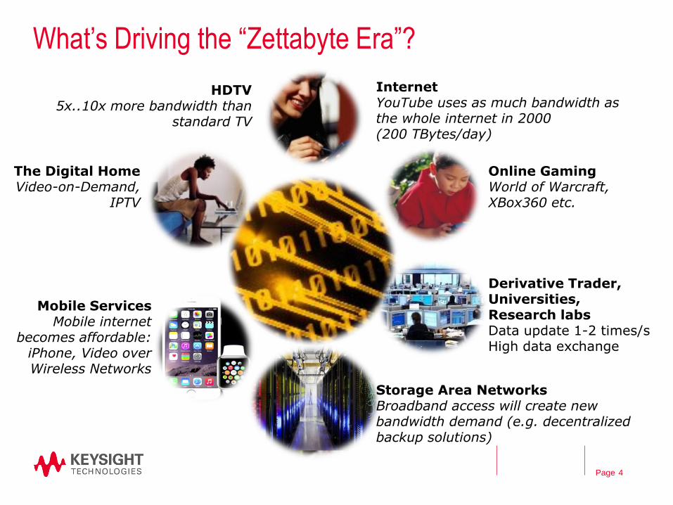
What’s Driving the “Zettabyte Era”?
HDTV 5x..10x more bandwidth than
standard TV
Internet YouTube uses as much bandwidth as the whole internet in 2000 (200 TBytes/day)
Online Gaming World of Warcraft, XBox360 etc.
Derivative Trader, Universities, Research labs Data update 1-2 times/s High data exchange
Mobile Services Mobile internet
becomes affordable: iPhone, Video over Wireless Networks
Storage Area Networks Broadband access will create new bandwidth demand (e.g. decentralized backup solutions)
The Digital Home Video-on-Demand,
IPTV
Motivation
Page
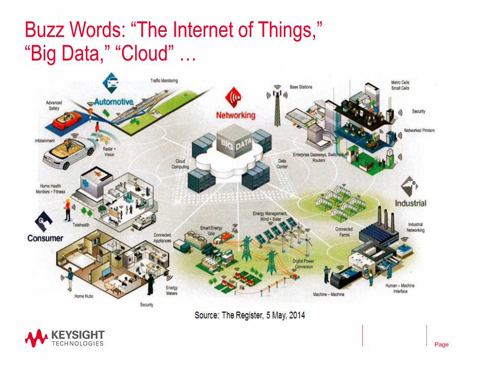
Buzz Words: “The Internet of Things,” “Big Data,” “Cloud” …
Page
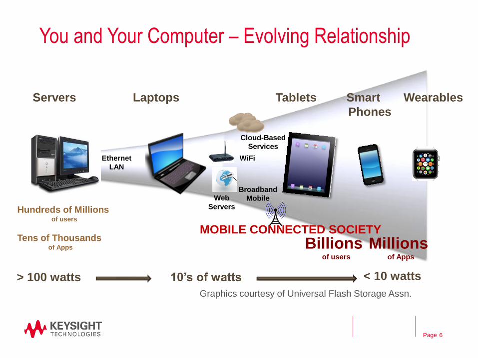
You and Your Computer – Evolving Relationship
6
Hundreds of Millions of users
Billions of users
Tens of Thousands of Apps Millions
of Apps
Ethernet
LAN
Broadband
Mobile
Cloud-Based
Services
> 100 watts 10’s of watts < 10 watts
WiFi
Web
Servers
MOBILE CONNECTED SOCIETY
Graphics courtesy of Universal Flash Storage Assn.
Servers Laptops Tablets Smart Wearables
Phones
Page
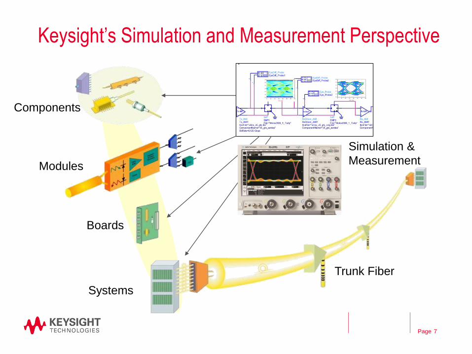
Keysight’s Simulation and Measurement Perspective
7
Components
Boards
Systems
Modules
Trunk Fiber
Simulation &
Measurement
Page 8
What are some enabling technologies to help us get to the “Zettabyte Era”?
Page
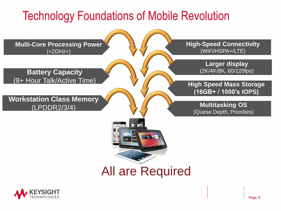
Technology Foundations of Mobile Revolution
9
All are Required
Multi-Core Processing Power (+2GHz+)
Workstation Class Memory
(LPDDR2/3/4)
Larger display (2K/4K/8K, 60/120fps)
High-Speed Connectivity (WiFi/HSPA+/LTE)
Battery Capacity
(8+ Hour Talk/Active Time)
Multitasking OS (Quese Depth, Priorities)
High Speed Mass Storage
(16GB+ / 1000’s IOPS)
Page
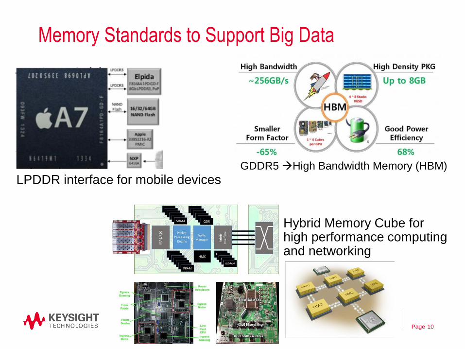
Memory Standards to Support Big Data
10
LPDDR interface for mobile devices
Hybrid Memory Cube for high performance computing and networking
GDDR5 High Bandwidth Memory (HBM)
Page 11
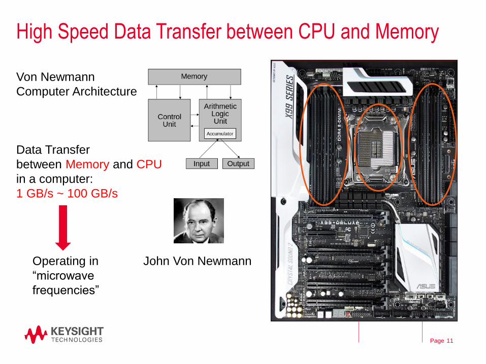
High Speed Data Transfer between CPU and Memory
John Von Newmann
Von Newmann
Computer Architecture
Data Transfer
between Memory and CPU
in a computer:
1 GB/s ~ 100 GB/s
Operating in
“microwave
frequencies”
Page
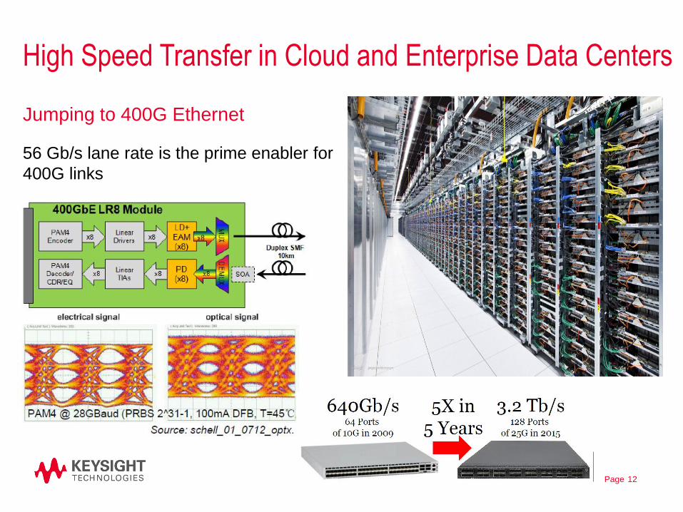
High Speed Transfer in Cloud and Enterprise Data Centers
12
Jumping to 400G Ethernet
56 Gb/s lane rate is the prime enabler for
400G links
Page
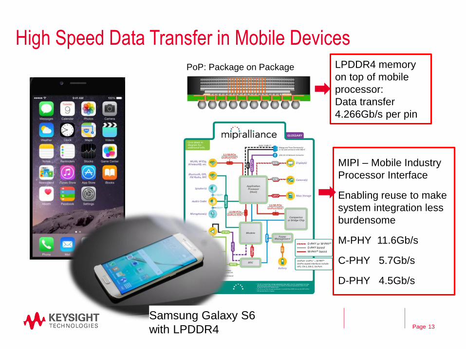
High Speed Data Transfer in Mobile Devices
13
PoP: Package on Package LPDDR4 memory
on top of mobile
processor:
Data transfer
4.266Gb/s per pin
MIPI – Mobile Industry
Processor Interface
Enabling reuse to make
system integration less
burdensome
M-PHY 11.6Gb/s
C-PHY 5.7Gb/s
D-PHY 4.5Gb/s
Samsung Galaxy S6
with LPDDR4

Page
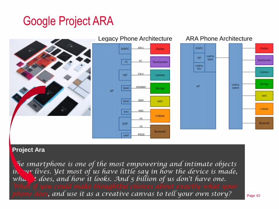
Google Project ARA
Project Ara
The smartphone is one of the most empowering and intimate objects in our lives. Yet most of us have little say in how the device is made, what it does, and how it looks. And 5 billion of us don't have one. What if you could make thoughtful choices about exactly what your phone does, and use it as a creative canvas to tell your own story? 14
Page 15
So what are some design challenges as we move towards the “Zettabyte Era”?
Page
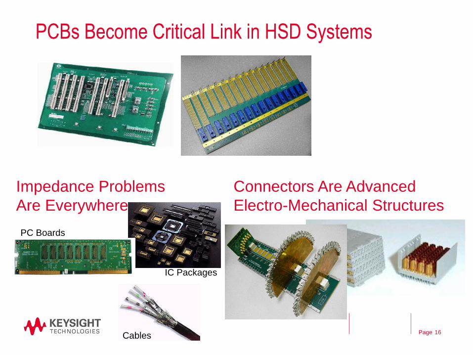
PCBs Become Critical Link in HSD Systems
16
IC Packages
Cables
PC Boards
Impedance Problems
Are Everywhere
Connectors Are Advanced
Electro-Mechanical Structures
Page
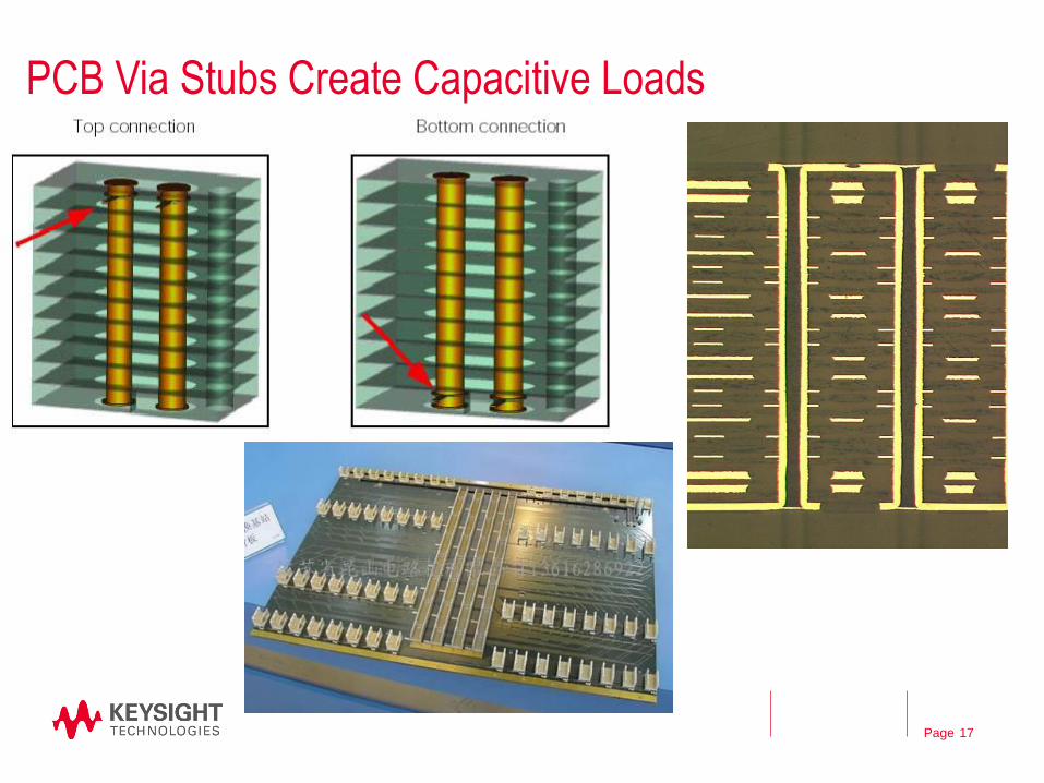
PCB Via Stubs Create Capacitive Loads
17
Page
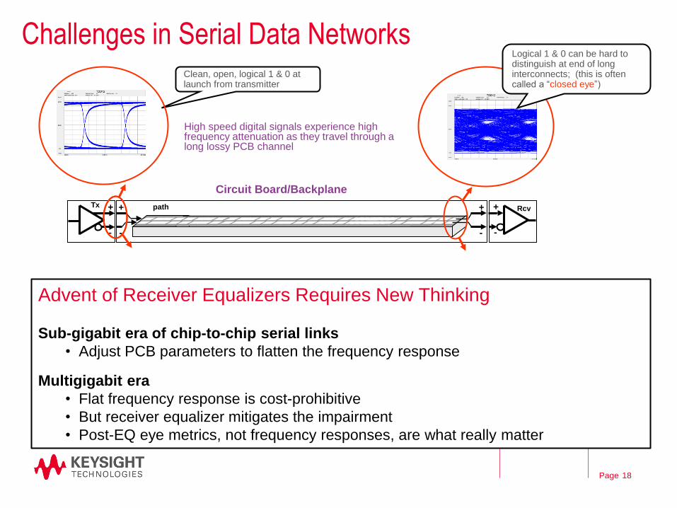
Challenges in Serial Data Networks
Tx +
-
+
-
Rcv path +
-
+
-
Clean, open, logical 1 & 0 at launch from transmitter
Circuit Board/Backplane
High speed digital signals experience high frequency attenuation as they travel through a long lossy PCB channel
Logical 1 & 0 can be hard to distinguish at end of long interconnects; (this is often called a “closed eye”)
18
Advent of Receiver Equalizers Requires New Thinking
Sub-gigabit era of chip-to-chip serial links
• Adjust PCB parameters to flatten the frequency response
Multigigabit era
• Flat frequency response is cost-prohibitive
• But receiver equalizer mitigates the impairment
• Post-EQ eye metrics, not frequency responses, are what really matter
Page
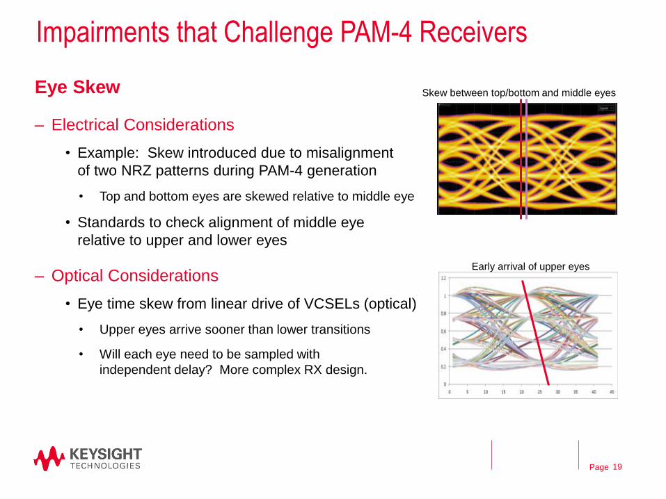
Impairments that Challenge PAM-4 Receivers
Eye Skew
– Electrical Considerations
• Example: Skew introduced due to misalignment
of two NRZ patterns during PAM-4 generation
• Top and bottom eyes are skewed relative to middle eye
• Standards to check alignment of middle eye
relative to upper and lower eyes
– Optical Considerations
• Eye time skew from linear drive of VCSELs (optical)
• Upper eyes arrive sooner than lower transitions
• Will each eye need to be sampled with
independent delay? More complex RX design.
19
Skew between top/bottom and middle eyes
Early arrival of upper eyes
Page
20
Page 21
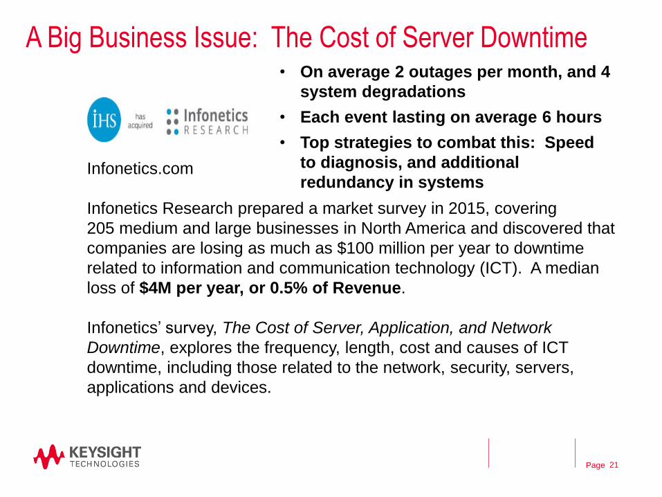
A Big Business Issue: The Cost of Server Downtime
Infonetics.com
Infonetics Research prepared a market survey in 2015, covering
205 medium and large businesses in North America and discovered that
companies are losing as much as $100 million per year to downtime
related to information and communication technology (ICT). A median
loss of $4M per year, or 0.5% of Revenue.
Infonetics’ survey, The Cost of Server, Application, and Network
Downtime, explores the frequency, length, cost and causes of ICT
downtime, including those related to the network, security, servers,
applications and devices.
• On average 2 outages per month, and 4
system degradations
• Each event lasting on average 6 hours
• Top strategies to combat this: Speed
to diagnosis, and additional
redundancy in systems
Page
Agenda
– High Speed Digital (HSD) Trends and Enabling Technologies
– HSD Basics
• Transmission lines, S-parameters, TDR/TDT
• Transceiver architectures and models
• Signal Integrity (SI), Power Integrity (PI), EMI, EMC
– Memory interfaces: DDR4/LPDDR4 and beyond
– MIPI (mobile industry processor interface) in mobile devices
– Ethernet interfaces in 10G~400G networking systems
– Summary
22
Page
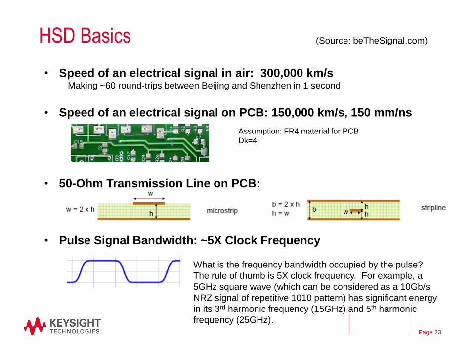
HSD Basics
23
• Speed of an electrical signal in air: 300,000 km/s Making ~60 round-trips between Beijing and Shenzhen in 1 second
• Speed of an electrical signal on PCB: 150,000 km/s, 150 mm/ns
• 50-Ohm Transmission Line on PCB:
• Pulse Signal Bandwidth: ~5X Clock Frequency
Assumption: FR4 material for PCB
Dk=4
(Source: beTheSignal.com)
What is the frequency bandwidth occupied by the pulse?
The rule of thumb is 5X clock frequency. For example, a
5GHz square wave (which can be considered as a 10Gb/s
NRZ signal of repetitive 1010 pattern) has significant energy
in its 3rd harmonic frequency (15GHz) and 5th harmonic
frequency (25GHz).
Page
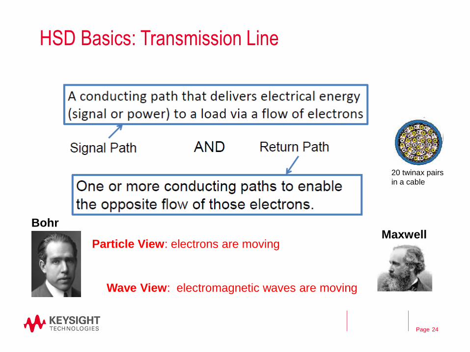
HSD Basics: Transmission Line
24
Particle View: electrons are moving
Wave View: electromagnetic waves are moving
20 twinax pairs
in a cable
Bohr Maxwell
Page
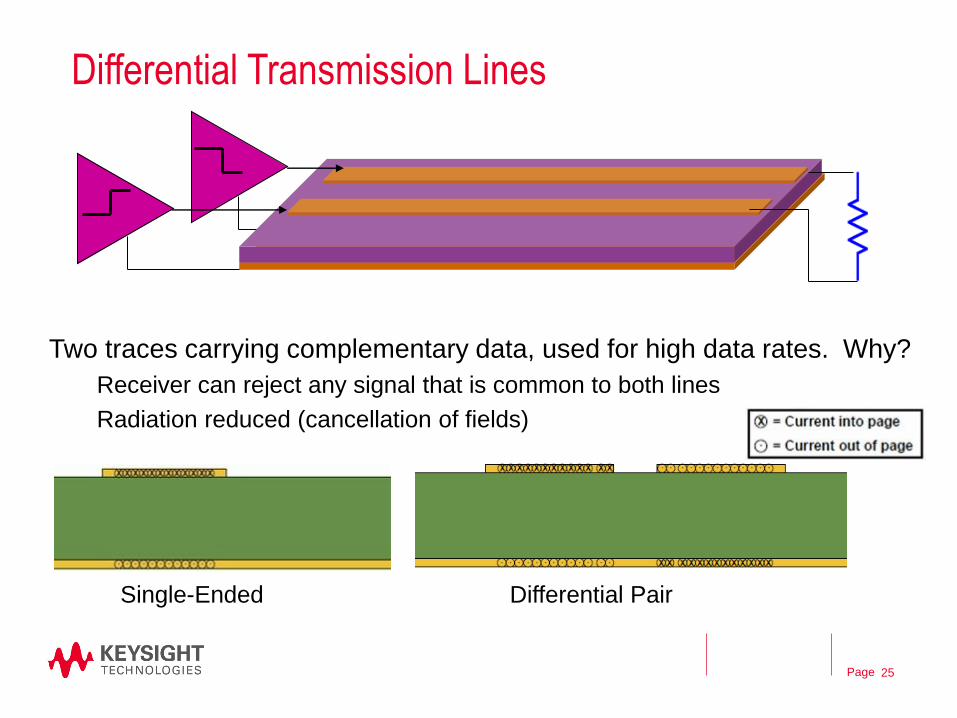
Differential Transmission Lines
25
Two traces carrying complementary data, used for high data rates. Why?
Receiver can reject any signal that is common to both lines
Radiation reduced (cancellation of fields)
Single-Ended Differential Pair
Page
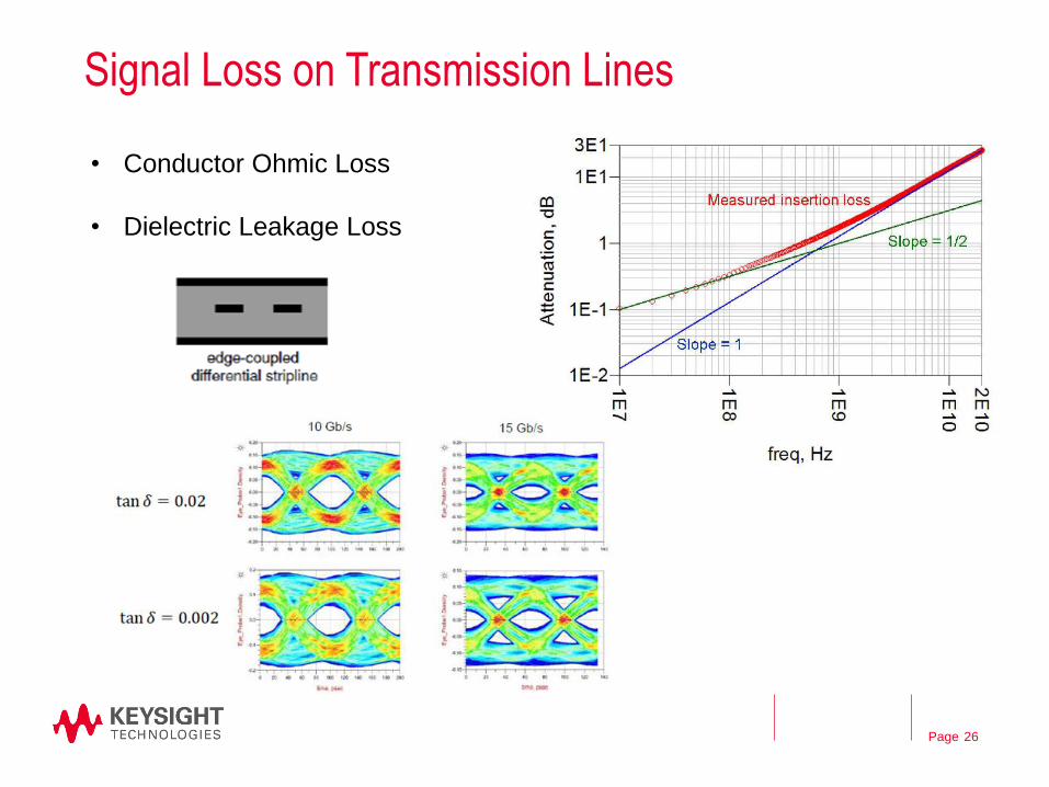
Signal Loss on Transmission Lines
26
• Conductor Ohmic Loss
• Dielectric Leakage Loss
Page
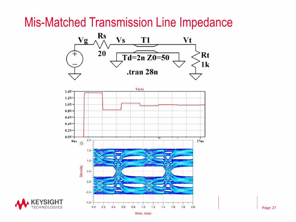
Mis-Matched Transmission Line Impedance
27
Page
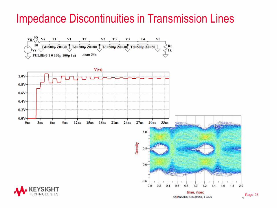
Impedance Discontinuities in Transmission Lines
28
Page
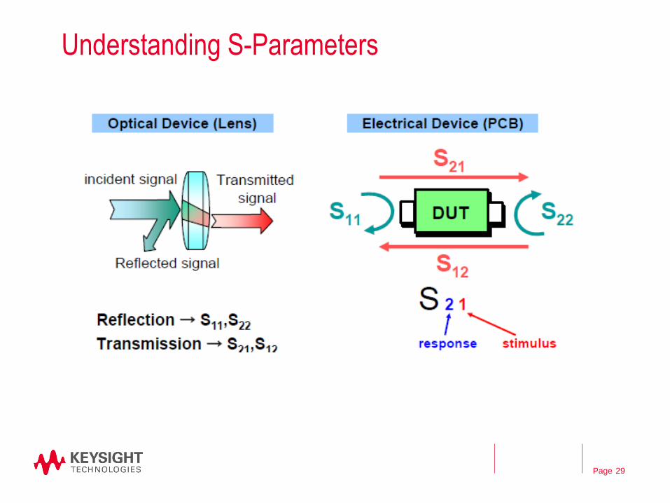
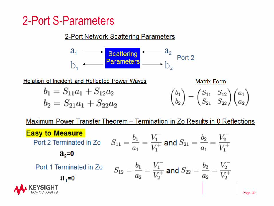
Understanding S-Parameters
29
Page
2-Port S-Parameters
30
Page
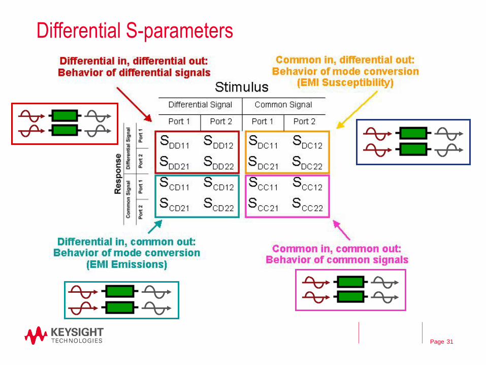
Differential S-parameters
31
Page
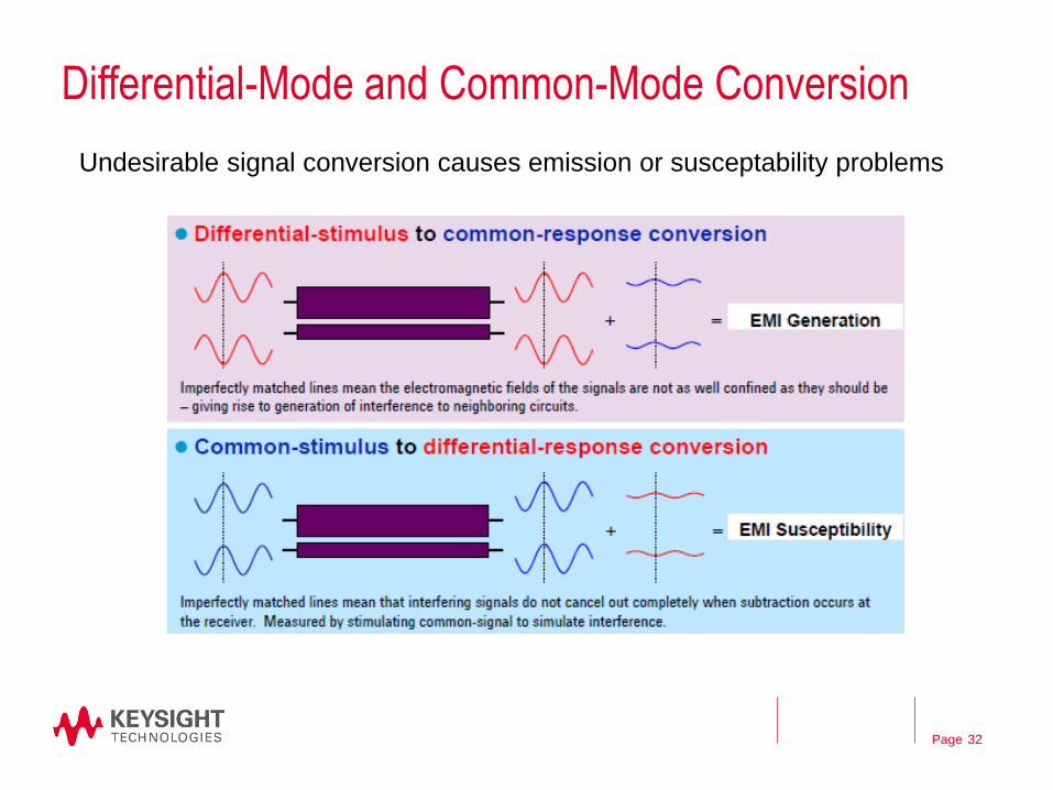
Differential-Mode and Common-Mode Conversion
Undesirable signal conversion causes emission or susceptability problems
32
Page
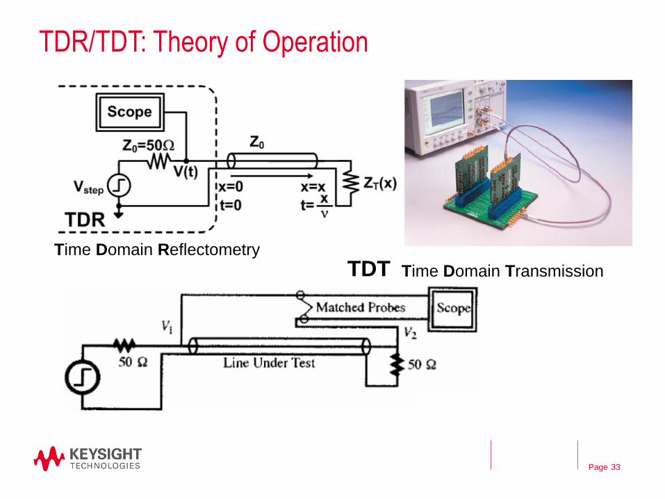
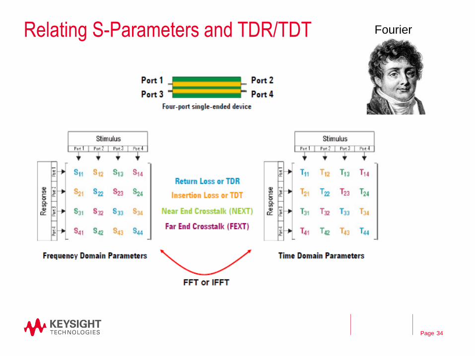
TDR/TDT: Theory of Operation
TDT Time Domain Reflectometry
Time Domain Transmission
33
Page
Relating S-Parameters and TDR/TDT Fourier
34
Page
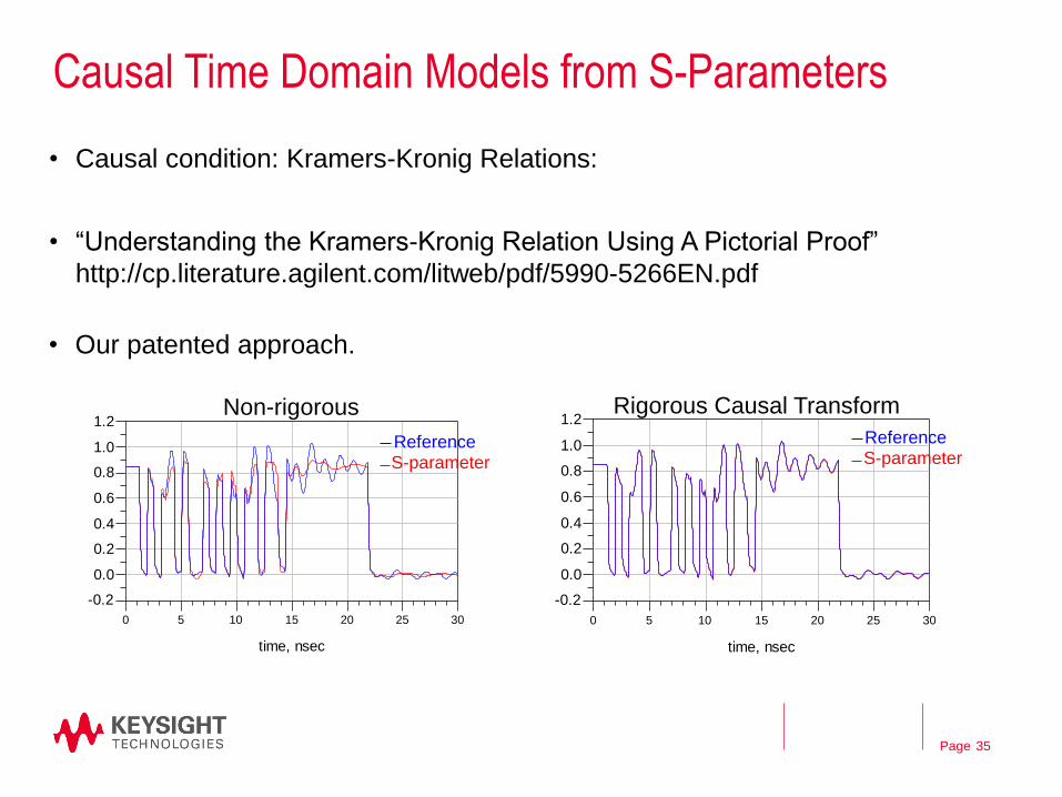
Causal Time Domain Models from S-Parameters
• Causal condition: Kramers-Kronig Relations:
• “Understanding the Kramers-Kronig Relation Using A Pictorial Proof”
http://cp.literature.agilent.com/litweb/pdf/5990-5266EN.pdf
• Our patented approach.
5 10 15 20 250 30
0.0
0.2
0.4
0.6
0.8
1.0
-0.2
1.2
time, nsec
Voutv
_S
, V
Voutv
, V
5 10 15 20 250 30
0.0
0.2
0.4
0.6
0.8
1.0
-0.2
1.2
time, nsec
Voutv
_S
, V
Voutv
, V
Non-rigorous Rigorous Causal Transform
S-parameter S-parameter Reference Reference
35
Page
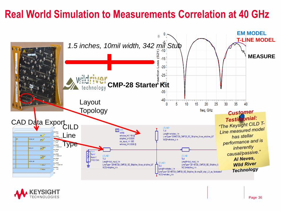
Real World Simulation to Measurements Correlation at 40 GHz
36
T-LINE MODEL
MEASURE
EM MODEL
1.5 inches, 10mil width, 342 mil Stub
CMP-28 Starter Kit
CAD Data Export CILD
Line
Type
Layout
Topology
Page
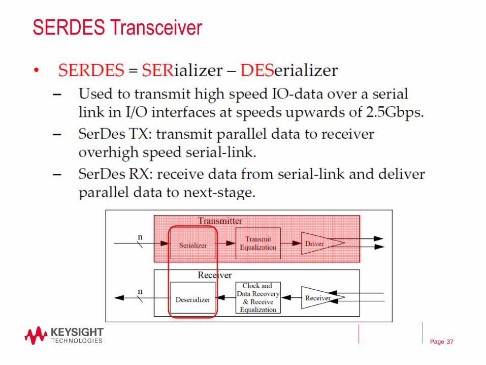
SERDES Transceiver
37
Page
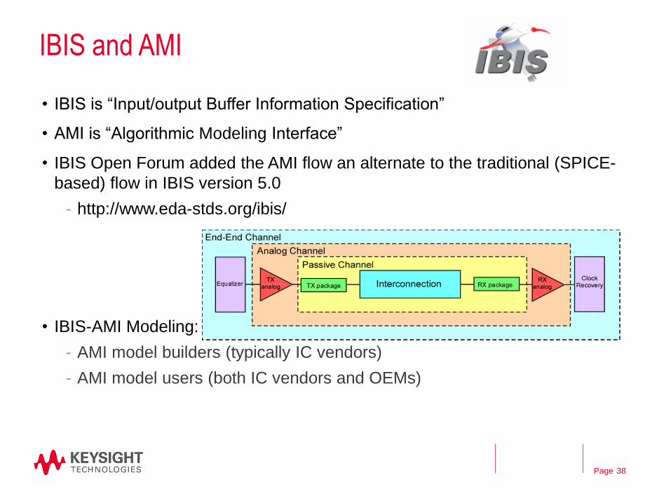
IBIS and AMI
• IBIS is “Input/output Buffer Information Specification”
• AMI is “Algorithmic Modeling Interface”
• IBIS Open Forum added the AMI flow an alternate to the traditional (SPICE-
based) flow in IBIS version 5.0
- http://www.eda-stds.org/ibis/
• IBIS-AMI Modeling:
- AMI model builders (typically IC vendors)
- AMI model users (both IC vendors and OEMs)
38
Page
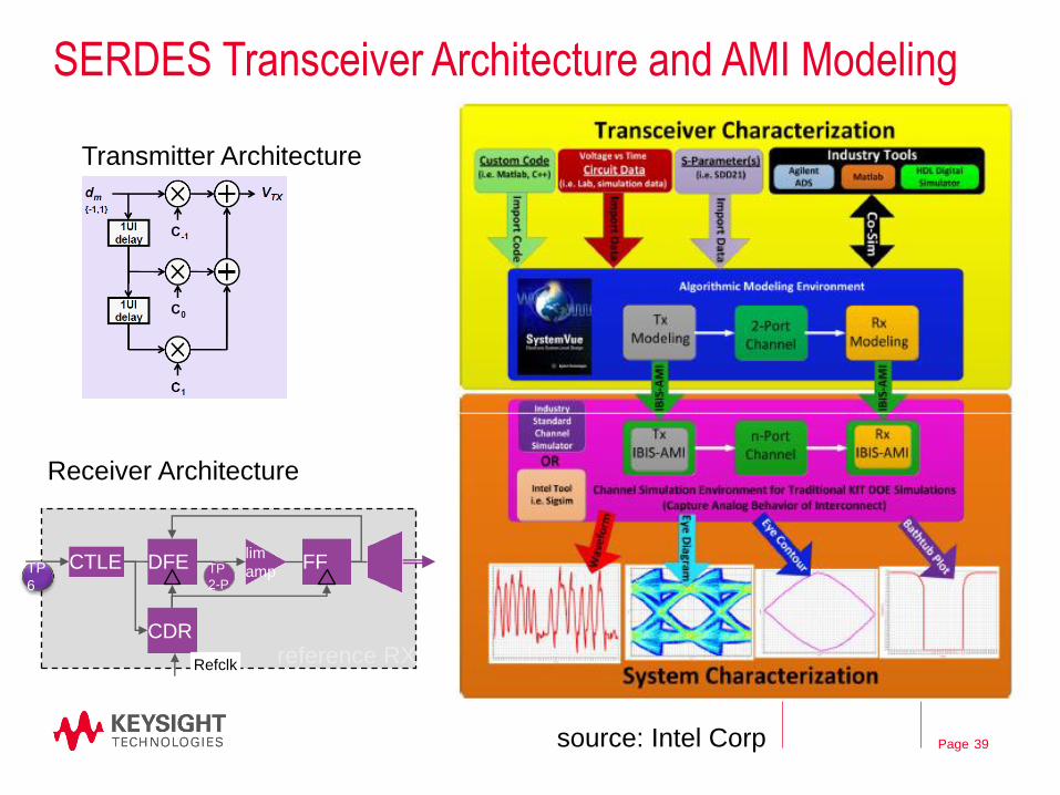
SERDES Transceiver Architecture and AMI Modeling
39
reference RX
FF lim
amp
CDR
CTLE DFE TP
6
TP
2-P
Refclk
Receiver Architecture
Transmitter Architecture
source: Intel Corp
Page
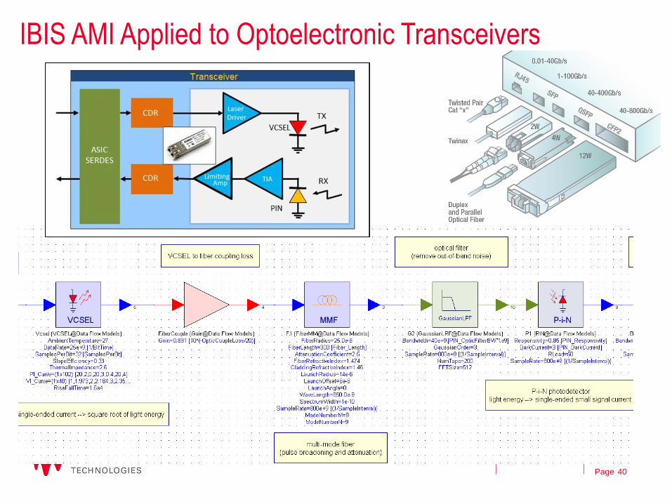
IBIS AMI Applied to Optoelectronic Transceivers
40
Page
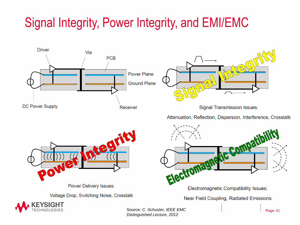
Signal Integrity, Power Integrity, and EMI/EMC
41 Source: C. Schuster, IEEE EMC
Distinguished Lecture, 2012
Page
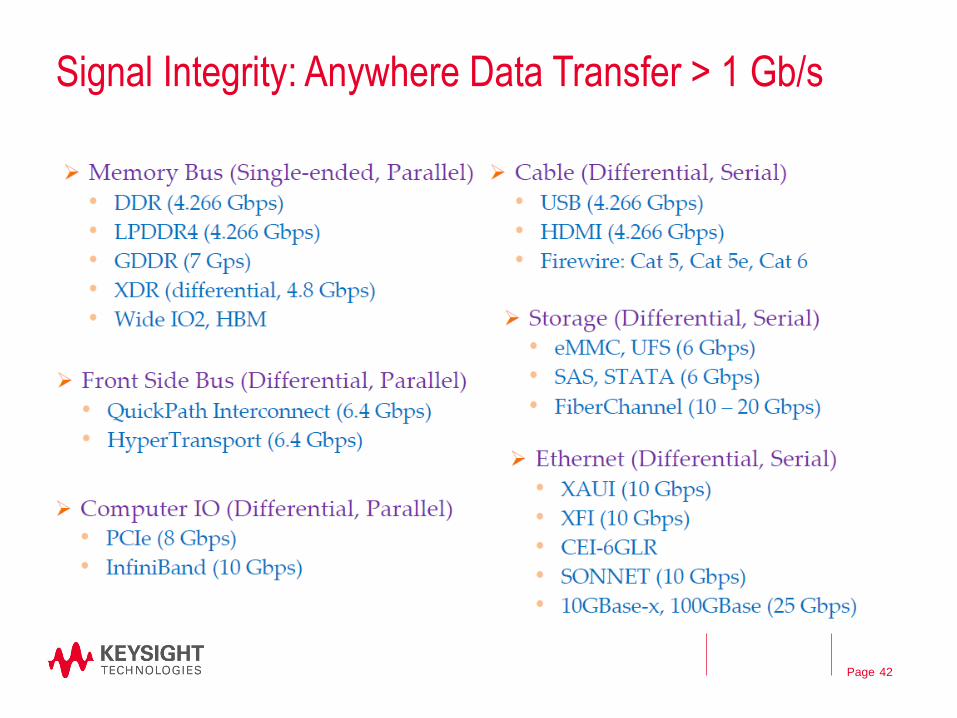
Signal Integrity: Anywhere Data Transfer > 1 Gb/s
42
Page
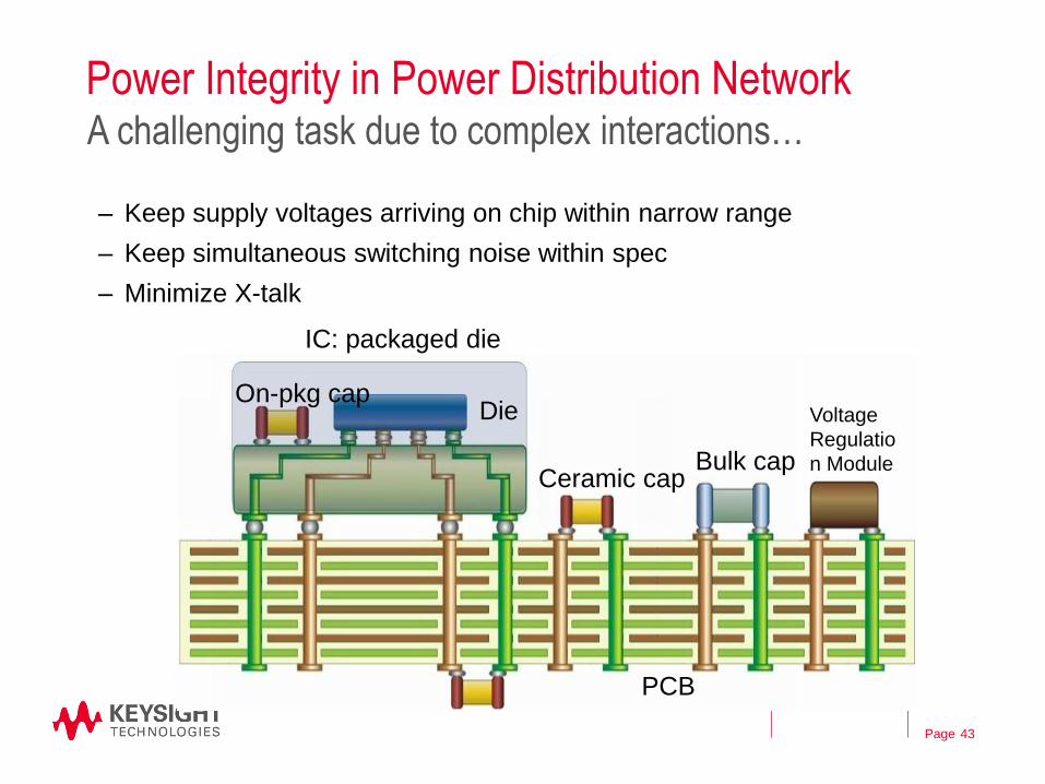
PCB
IC: packaged die
Voltage
Regulatio
n Module Bulk cap Ceramic cap
On-pkg cap Die
Power Integrity in Power Distribution Network
– Keep supply voltages arriving on chip within narrow range
– Keep simultaneous switching noise within spec
– Minimize X-talk
A challenging task due to complex interactions…
43
Page
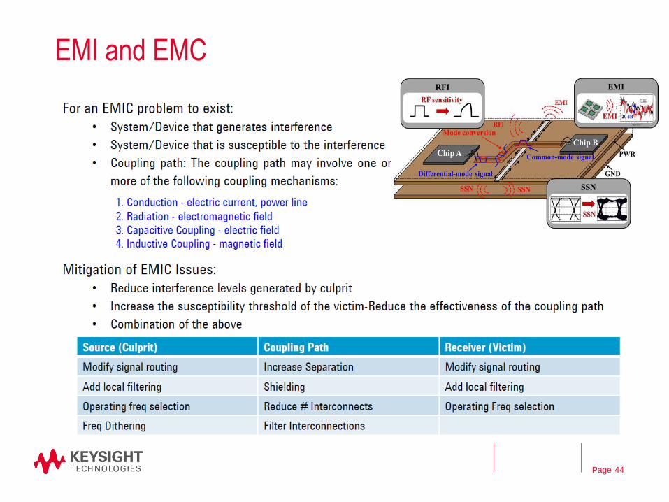
EMI and EMC
44
Page
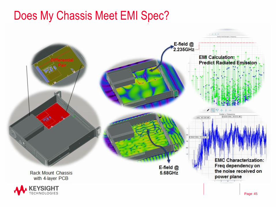
Does My Chassis Meet EMI Spec?
45
Page
SI PI
EMI
EMC Thermal
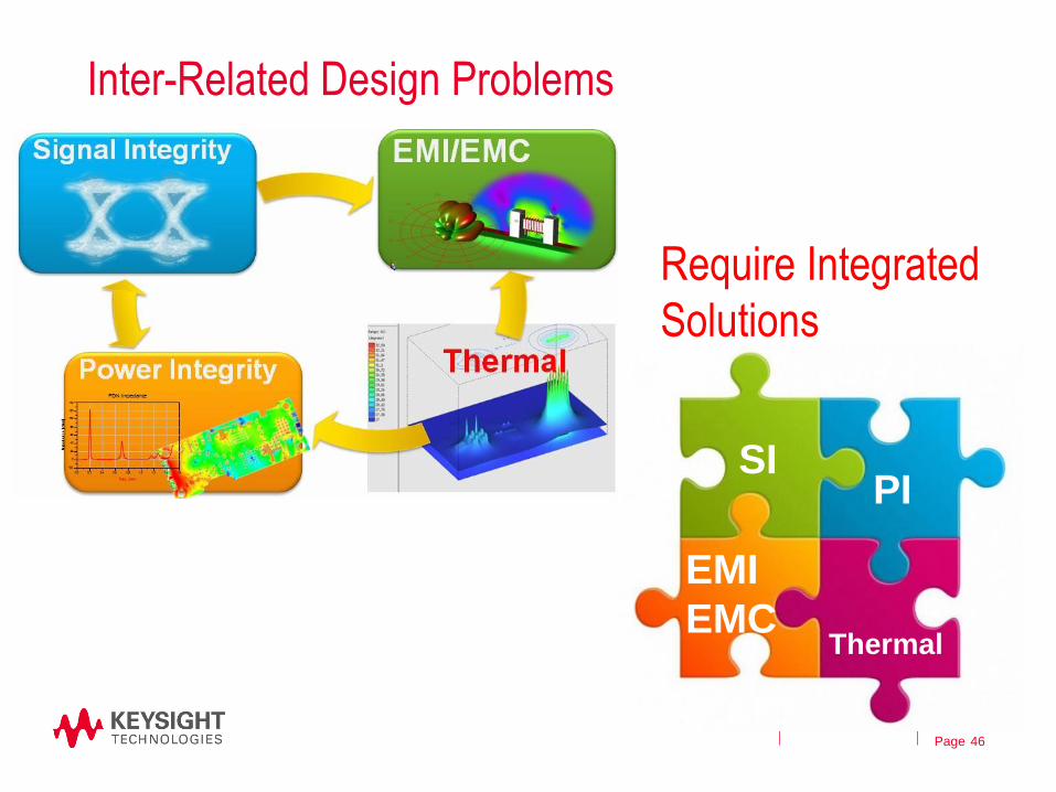
Inter-Related Design Problems
46
Require Integrated
Solutions
Page
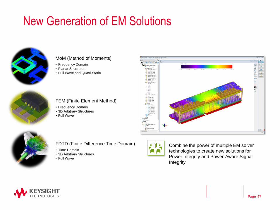
New Generation of EM Solutions
47
• Frequency Domain
• Planar Structures
• Full Wave and Quasi-Static
• Frequency Domain
• 3D Arbitrary Structures
• Full Wave
• Time Domain
• 3D Arbitrary Structures
• Full Wave
FDTD (Finite Difference Time Domain)
FEM (Finite Element Method)
MoM (Method of Moments)
Combine the power of multiple EM solver
technologies to create new solutions for
Power Integrity and Power-Aware Signal
Integrity
Page
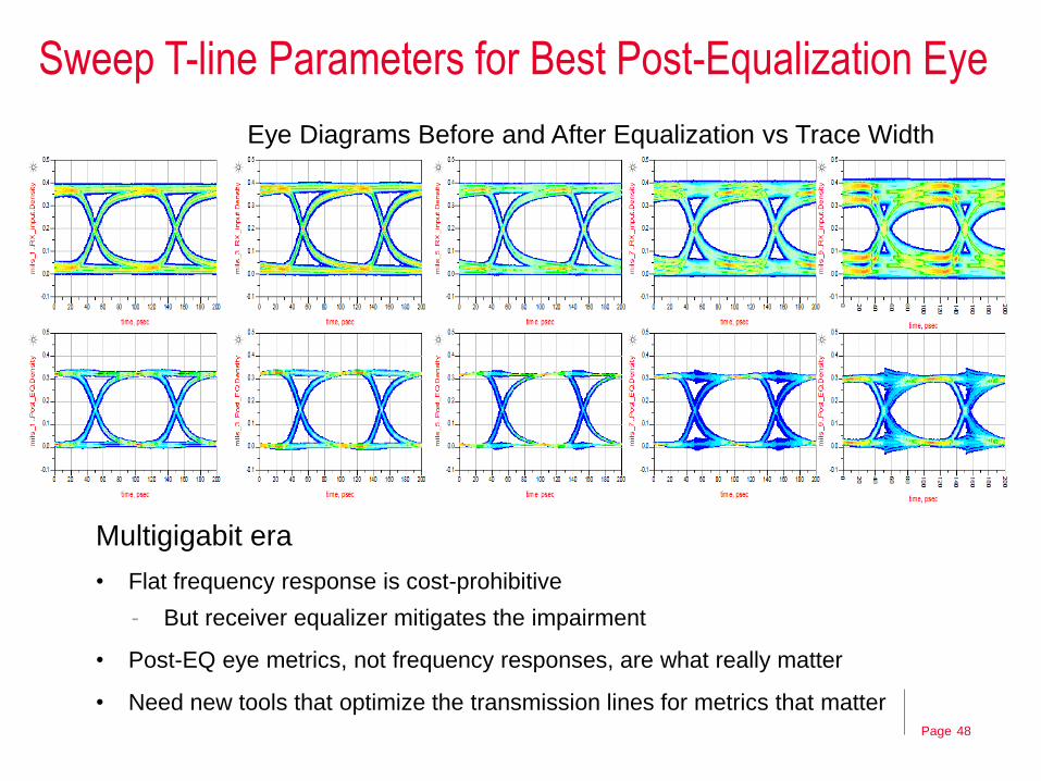
Sweep T-line Parameters for Best Post-Equalization Eye
48
Eye Diagrams Before and After Equalization vs Trace Width
Multigigabit era
• Flat frequency response is cost-prohibitive
- But receiver equalizer mitigates the impairment
• Post-EQ eye metrics, not frequency responses, are what really matter
• Need new tools that optimize the transmission lines for metrics that matter
Page
Agenda
– High Speed Digital (HSD) Trends and Enabling Technologies
– HSD Basics
• Transmission lines, S-parameters, TDR/TDT
• Transceiver architectures and models
• Signal Integrity (SI), Power Integrity (PI), EMI, EMC
– Memory interfaces: DDR4/LPDDR4 and beyond
– MIPI (mobile industry processor interface) in mobile devices
– Ethernet interfaces in 10G~400G networking systems
– Summary
49
Page
100
200
400
800
1600
3200
6400
12800
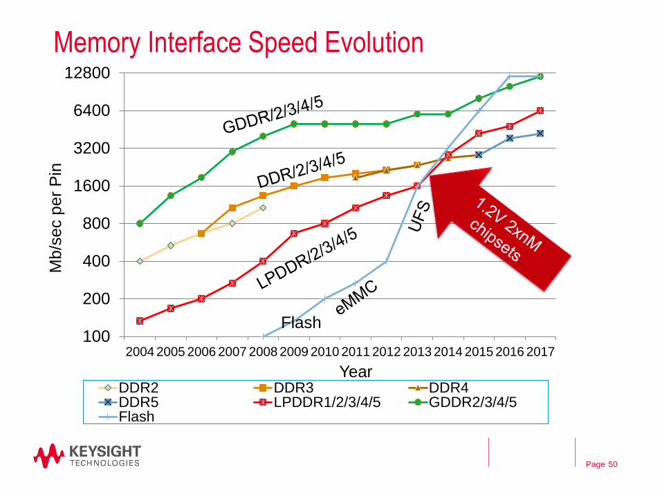
2004 2005 2006 2007 2008 2009 2010 2011 2012 2013 2014 2015 2016 2017
DDR2 DDR3 DDR4DDR5 LPDDR1/2/3/4/5 GDDR2/3/4/5Flash
Mb/s
ec p
er
Pin
Year
Memory Interface Speed Evolution
50
Flash
Page
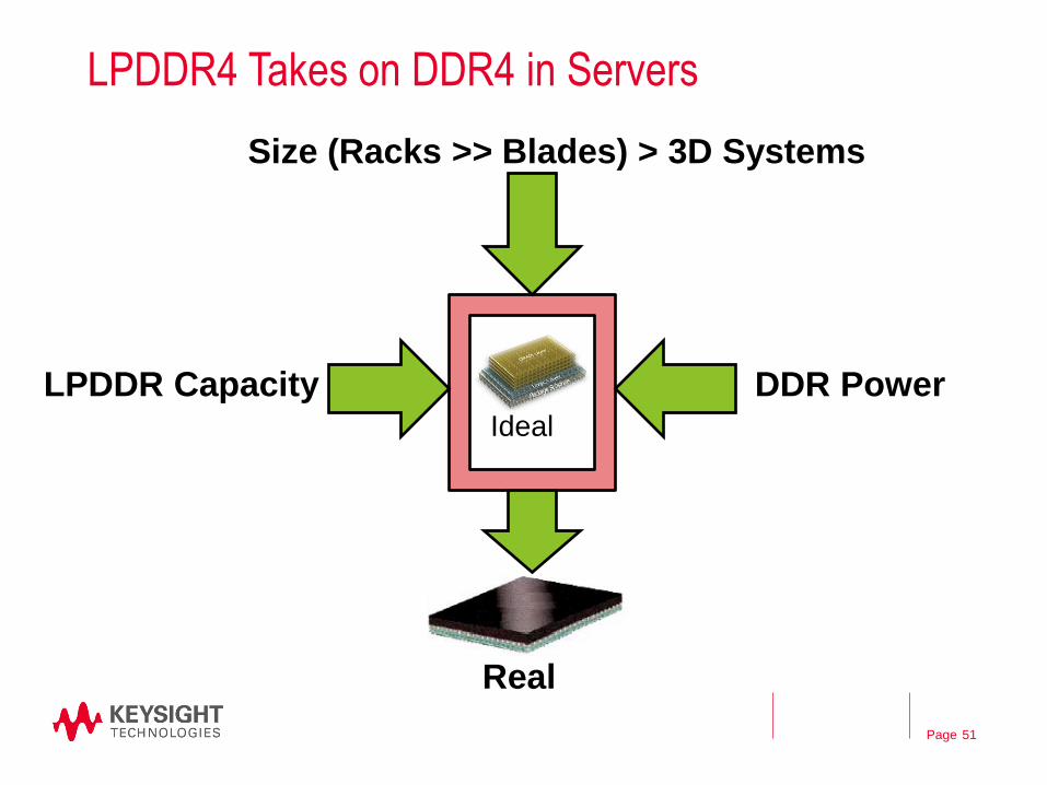
LPDDR4 Takes on DDR4 in Servers
51
LPDDR Capacity
Size (Racks >> Blades) > 3D Systems
DDR Power
Real
Ideal
Page
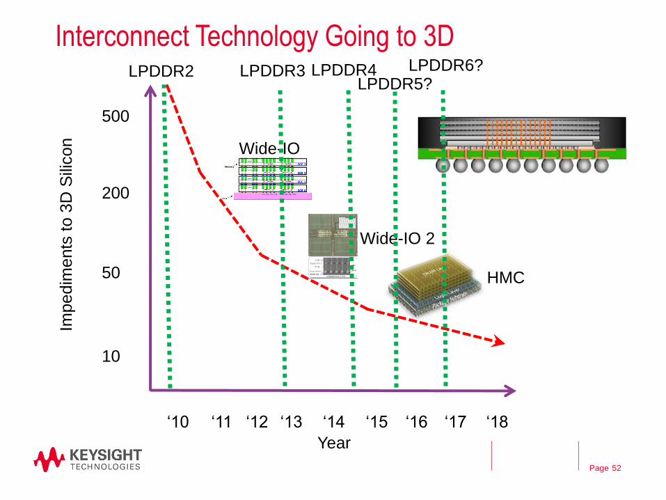
Interconnect Technology Going to 3D
52
Year
Impedim
ents
to 3
D S
ilicon
LPDDR2
‘10 ‘11 ‘12 ‘13 ‘14 ‘15 ‘16 ‘17 ‘18
500
10
50
200
Wide-IO
Wide-IO 2
HMC
LPDDR3 LPDDR4 LPDDR5?
LPDDR6?
Page
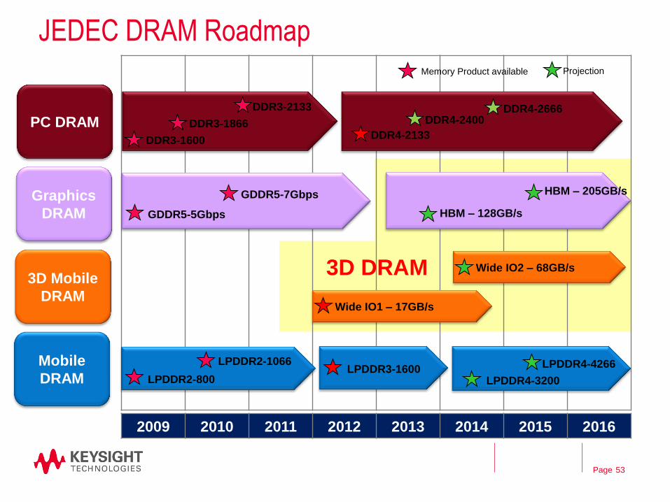
JEDEC DRAM Roadmap
2009 2010 2011 2012 2013 2014 2015 2016
PC DRAM
Graphics
DRAM
3D Mobile
DRAM
Mobile
DRAM
DDR3-1600
DDR3-1866
DDR3-2133
DDR4-2133
GDDR5-5Gbps
GDDR5-7Gbps
HBM – 128GB/s
HBM – 205GB/s
Memory Product available Projection
Wide IO1 – 17GB/s
Wide IO2 – 68GB/s
LPDDR2-800
LPDDR2-1066 LPDDR3-1600
LPDDR4-3200
LPDDR4-4266
3D DRAM
DDR4-2400 DDR4-2666
53
Page
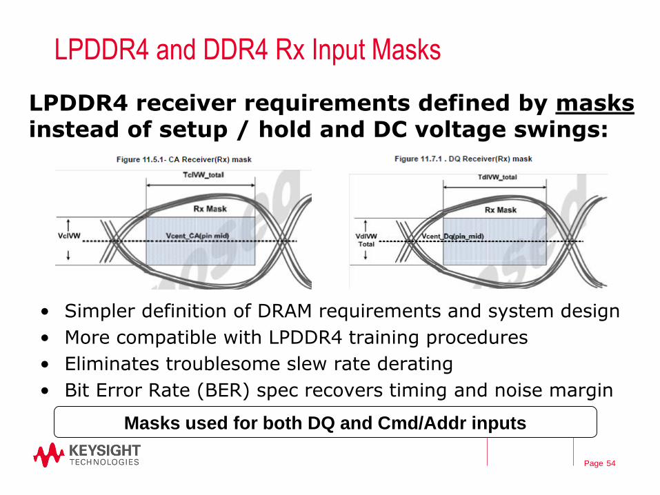
LPDDR4 and DDR4 Rx Input Masks
• Simpler definition of DRAM requirements and system design
• More compatible with LPDDR4 training procedures
• Eliminates troublesome slew rate derating
• Bit Error Rate (BER) spec recovers timing and noise margin
LPDDR4 receiver requirements defined by masks instead of setup / hold and DC voltage swings:
Masks used for both DQ and Cmd/Addr inputs
54
Page
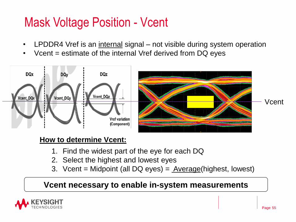
Mask Voltage Position - Vcent
55
1. Find the widest part of the eye for each DQ
2. Select the highest and lowest eyes
3. Vcent = Midpoint (all DQ eyes) = Average(highest, lowest)
Vcent
• LPDDR4 Vref is an internal signal – not visible during system operation
• Vcent = estimate of the internal Vref derived from DQ eyes
Vcent necessary to enable in-system measurements
How to determine Vcent:
Page
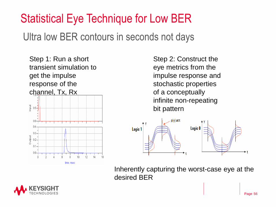
Statistical Eye Technique for Low BER
56
Ultra low BER contours in seconds not days
Step 1: Run a short
transient simulation to
get the impulse
response of the
channel, Tx, Rx
Step 2: Construct the
eye metrics from the
impulse response and
stochastic properties
of a conceptually
infinite non-repeating
bit pattern
Inherently capturing the worst-case eye at the
desired BER
Page
Finding the Worst Case Bit Pattern ? What about Crosstalk?
Showing the responses of the
two closest crosstalk channels.
By the time the 10th bit enters
the channel, the energy from
the 1st bit has left the channel
There are 29 possible bit
patterns that could result in the
worst-case eye (512).
We should at least consider 4
Xtalk aggressors (2 either side).
Leaving 2(6+Nxtlk*9) = 4e12 bit
patterns!!
57
Page
58
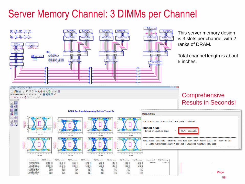
Server Memory Channel: 3 DIMMs per Channel
This server memory design
is 3 slots per channel with 2
ranks of DRAM.
Total channel length is about
5 inches.
Comprehensive
Results in Seconds!
Page
Agenda
– High Speed Digital (HSD) Trends and Enabling Technologies
– HSD Basics
• Transmission lines, S-parameters, TDR/TDT
• Transceiver architectures and models
• Signal Integrity (SI), Power Integrity (PI), EMI, EMC
– Memory interfaces: DDR4/LPDDR4 and beyond
– MIPI (mobile industry processor interface) in mobile devices
– Ethernet interfaces in 10G~400G networking systems
– Summary
59
Page
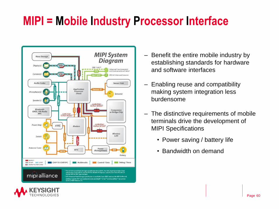
MIPI = Mobile Industry Processor Interface
– Benefit the entire mobile industry by
establishing standards for hardware
and software interfaces
– Enabling reuse and compatibility
making system integration less
burdensome
– The distinctive requirements of mobile
terminals drive the development of
MIPI Specifications
• Power saving / battery life
• Bandwidth on demand
60
MIPI M-PHY Receiver Test Webinar
August 2013
Page
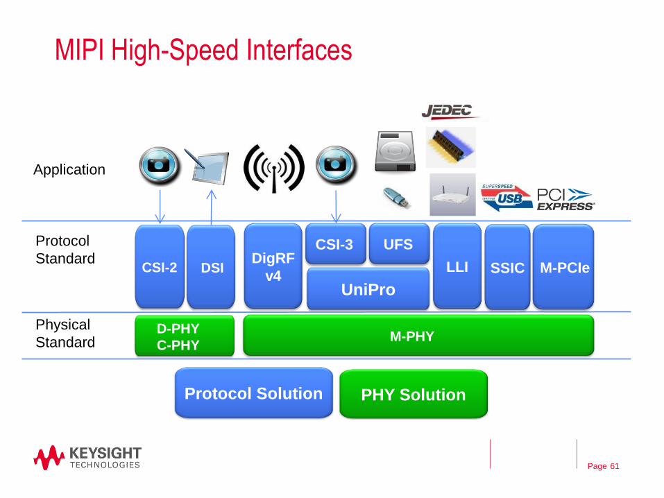
UniPro
UFS
Physical
Standard
Protocol
Standard
D-PHY
C-PHY
CSI-2 DSI DigRF
v4
M-PHY
Application
CSI-3
Protocol Solution PHY Solution
MIPI High-Speed Interfaces
LLI SSIC M-PCIe
61
Page
Google Project ARA
Project Ara
The smartphone is one of the most empowering and intimate objects in our lives. Yet most of us have little say in how the device is made, what it does, and how it looks. And 5 billion of us don't have one. What if you could make thoughtful choices about exactly what your phone does, and use it as a creative canvas to tell your own story? 62
Legacy Phone Architecture ARA Phone Architecture
Page
Why Three Different PHY-Layer Standards?
2013 and Before
– D-PHY
• Used for camera (CSI-2) and display (DSI) applications
• Electrical specifications allow usage of relatively inexpensive semiconductor process
– M-PHY
• Proposed high BW successor of D-PHY addressing camera and display applications
• Discrete data rates (Gears) up to approximately 12Gb/s; sufficient for quite a while
2014 Onwards
– C-PHY started
• New 3-wire / 3 level data format allowing transmission of >1 bit / symbol
• HS mode w/ toggle rates reaching continuously up to 2.5Gbaud / 5.75Gb/s
– D-PHY extended
• Rev. 1.2 w/ max data rate 2.5Gbs (achieved through RX deskew)
• Rev. 2.x started, data rate project beyond 4.5 Gb/s (6.5Gb/s)
63
Page
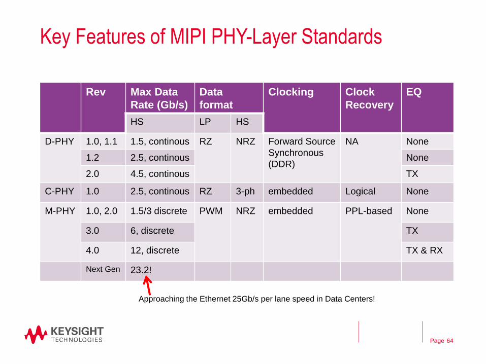
Key Features of MIPI PHY-Layer Standards
Rev Max Data
Rate (Gb/s)
Data
format
Clocking Clock
Recovery
EQ
HS LP HS
D-PHY 1.0, 1.1 1.5, continous RZ NRZ Forward Source
Synchronous
(DDR)
NA None
1.2 2.5, continous None
2.0 4.5, continous TX
C-PHY 1.0 2.5, continous RZ 3-ph embedded Logical None
M-PHY 1.0, 2.0 1.5/3 discrete PWM NRZ embedded PPL-based None
3.0 6, discrete TX
4.0 12, discrete TX & RX
Next Gen 23.2!
64
Approaching the Ethernet 25Gb/s per lane speed in Data Centers!
Page
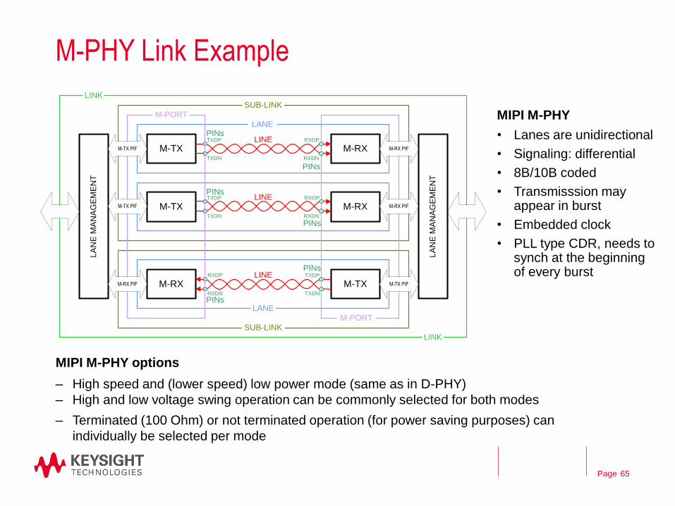
M-PHY Link Example
MIPI M-PHY options
– High speed and (lower speed) low power mode (same as in D-PHY)
– High and low voltage swing operation can be commonly selected for both modes
– Terminated (100 Ohm) or not terminated operation (for power saving purposes) can
individually be selected per mode
65
MIPI M-PHY
• Lanes are unidirectional
• Signaling: differential
• 8B/10B coded
• Transmisssion may appear in burst
• Embedded clock
• PLL type CDR, needs to synch at the beginning of every burst
M-TX
M-TX
M-RX
M-RX
M-TX
M-RX
LA
NE
MA
NA
GE
ME
NT
PINsLINE
LANE
LINK
PINsLINE
PINs
LINE
PINs
PINs
PINs
LA
NE
MA
NA
GE
ME
NT
TXDP
TXDN
RXDP
RXDN
TXDP
TXDN
TXDP
TXDN
RXDP
RXDN
RXDP
RXDN
SUB-LINK
LANE
SUB-LINK
LINK
M-TX PIF
M-TX PIF
M-RX PIF
M-RX PIF
M-RX PIF
M-TX PIF
M-PORT
M-PORT
Page
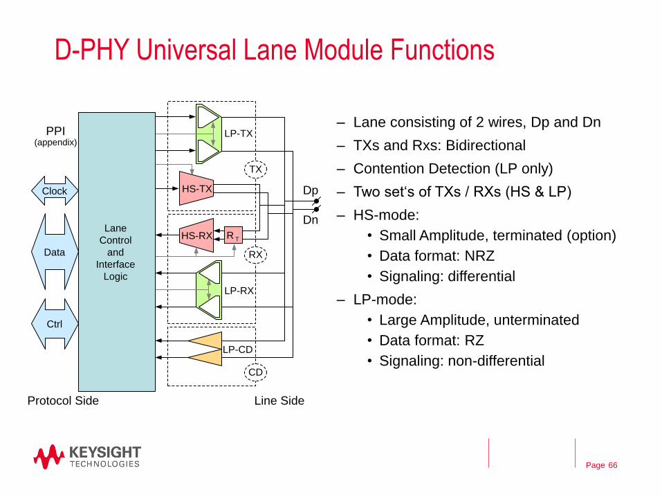
D-PHY Universal Lane Module Functions
– Lane consisting of 2 wires, Dp and Dn
– TXs and Rxs: Bidirectional
– Contention Detection (LP only)
– Two set‘s of TXs / RXs (HS & LP)
– HS-mode:
• Small Amplitude, terminated (option)
• Data format: NRZ
• Signaling: differential
– LP-mode:
• Large Amplitude, unterminated
• Data format: RZ
• Signaling: non-differential
66
RX
Dp
Dn
TX
LP-TX
HS-RX
CD
PPI(appendix)
RT
Data
Clock
Ctrl
Protocol Side
RTR T
Line Side
LP-RX
LP-CD
Lane
Control
and
Interface
Logic
HS-TX
Page
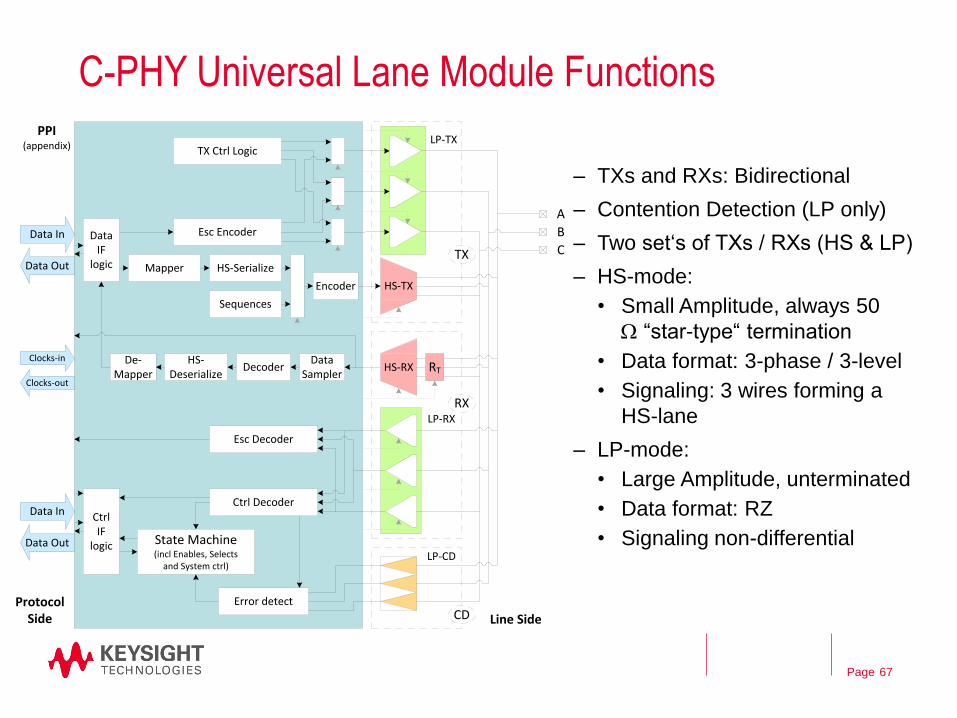
C-PHY Universal Lane Module Functions
– TXs and RXs: Bidirectional
– Contention Detection (LP only)
– Two set‘s of TXs / RXs (HS & LP)
– HS-mode:
• Small Amplitude, always 50
W “star-type“ termination
• Data format: 3-phase / 3-level
• Signaling: 3 wires forming a
HS-lane
– LP-mode:
• Large Amplitude, unterminated
• Data format: RZ
• Signaling non-differential
67
A
B
C
HS-TX
HS-RX RT
TX Ctrl Logic
DecoderHS-
Deserialize
State Machine(incl Enables, Selects
and System ctrl)
Error detect
CtrlIF
logic
DataIF
logic
Esc Encoder
HS-Serialize
Sequences
Mapper
Encoder
Data Sampler
Esc Decoder
Ctrl Decoder
Data Out
Data In
TX
RX
CD
Data Out
Data In
Clocks-out
Clocks-in
PPI(appendix)
ProtocolSide Line Side
De-Mapper
LP-TX
LP-RX
LP-CD
Page
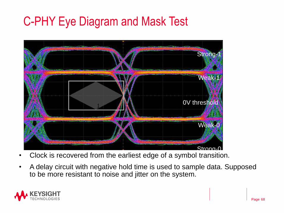
C-PHY Eye Diagram and Mask Test
68
• Clock is recovered from the earliest edge of a symbol transition.
• A delay circuit with negative hold time is used to sample data. Supposed to be more resistant to noise and jitter on the system.
Strong-1
Weak-1
Weak-0
Strong-0
0V threshold
Page
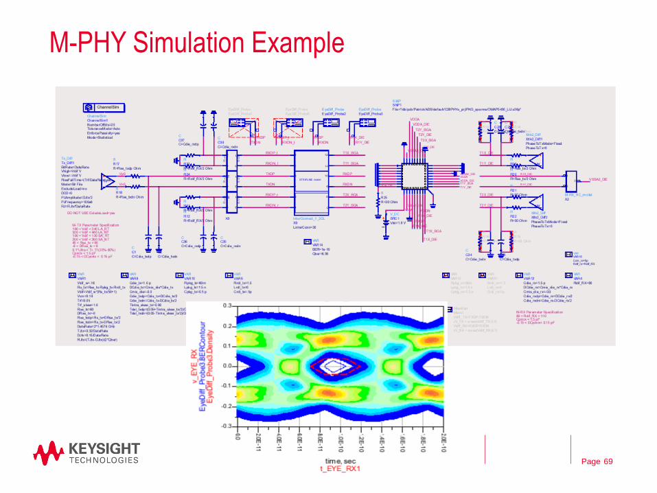
M-PHY Simulation Example
69
Page
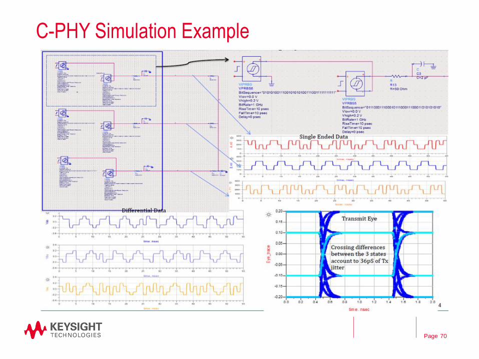
C-PHY Simulation Example
70
Page
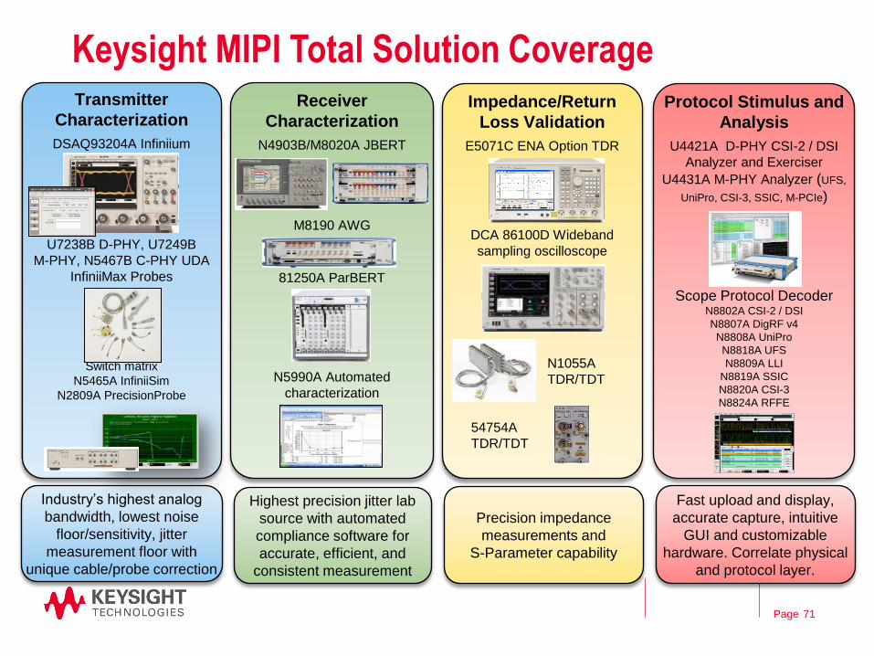
Keysight MIPI Total Solution Coverage Transmitter
Characterization
DSAQ93204A Infiniium
U7238B D-PHY, U7249B
M-PHY, N5467B C-PHY UDA
InfiniiMax Probes
Switch matrix
N5465A InfiniiSim
N2809A PrecisionProbe
Receiver
Characterization
N4903B/M8020A JBERT
M8190 AWG
81250A ParBERT
N5990A Automated
characterization
Impedance/Return
Loss Validation
E5071C ENA Option TDR
DCA 86100D Wideband
sampling oscilloscope
N1055A
TDR/TDT
54754A
TDR/TDT
Industry’s highest analog
bandwidth, lowest noise
floor/sensitivity, jitter
measurement floor with
unique cable/probe correction
Precision impedance
measurements and
S-Parameter capability
Highest precision jitter lab
source with automated
compliance software for
accurate, efficient, and
consistent measurement
Protocol Stimulus and
Analysis
U4421A D-PHY CSI-2 / DSI
Analyzer and Exerciser
U4431A M-PHY Analyzer (UFS,
UniPro, CSI-3, SSIC, M-PCIe)
Scope Protocol Decoder N8802A CSI-2 / DSI
N8807A DigRF v4
N8808A UniPro
N8818A UFS
N8809A LLI
N8819A SSIC
N8820A CSI-3
N8824A RFFE
Fast upload and display,
accurate capture, intuitive
GUI and customizable
hardware. Correlate physical
and protocol layer.
71
Page
Agenda
– High Speed Digital (HSD) Trends and Enabling Technologies
– HSD Basics
• Transmission lines, S-parameters, TDR/TDT
• Transceiver architectures and models
• Signal Integrity (SI), Power Integrity (PI), EMI, EMC
– Memory interfaces: DDR4/LPDDR4 and beyond
– MIPI (mobile industry processor interface) in mobile devices
– Ethernet interfaces in 10G~400G networking systems
– Summary
72
Page
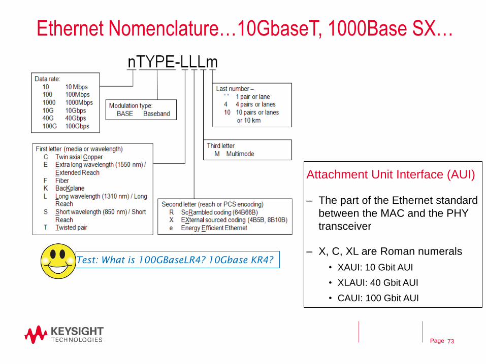
Ethernet Nomenclature…10GbaseT, 1000Base SX…
73
April, 2012
Test: What is 100GBaseLR4? 10Gbase KR4?
Attachment Unit Interface (AUI)
– The part of the Ethernet standard
between the MAC and the PHY
transceiver
– X, C, XL are Roman numerals
• XAUI: 10 Gbit AUI
• XLAUI: 40 Gbit AUI
• CAUI: 100 Gbit AUI
Page
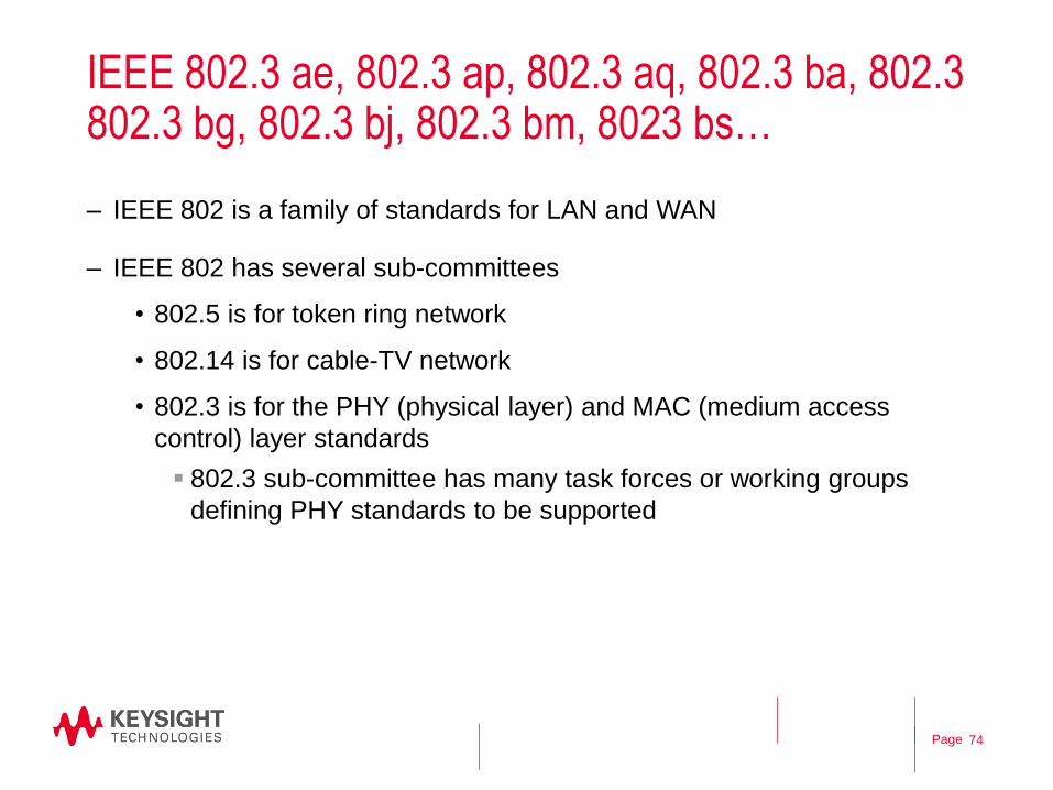
IEEE 802.3 ae, 802.3 ap, 802.3 aq, 802.3 ba, 802.3 802.3 bg, 802.3 bj, 802.3 bm, 8023 bs…
– IEEE 802 is a family of standards for LAN and WAN
– IEEE 802 has several sub-committees
• 802.5 is for token ring network
• 802.14 is for cable-TV network
• 802.3 is for the PHY (physical layer) and MAC (medium access
control) layer standards
802.3 sub-committee has many task forces or working groups
defining PHY standards to be supported
74
Page
Ethernet in Data Center Networking
Driven by Optical Internetworking Forum, IEEE, Fibre Channel, Infiniband
Food chain: Hosts (chips), Modules (optical transceivers), connectors &
backplanes, systems
Link speed – 100G (early deployment), 400G (2018) 1T (2021+?)
• Mostly optical multi-mode – lower cost ($50 - $150)
• Modern data center has 20,000 optical links
Considerable growth – # ports (27% CAGR), R & D investment $,
new vendors (= growing addressable market for T&M)
75
Page
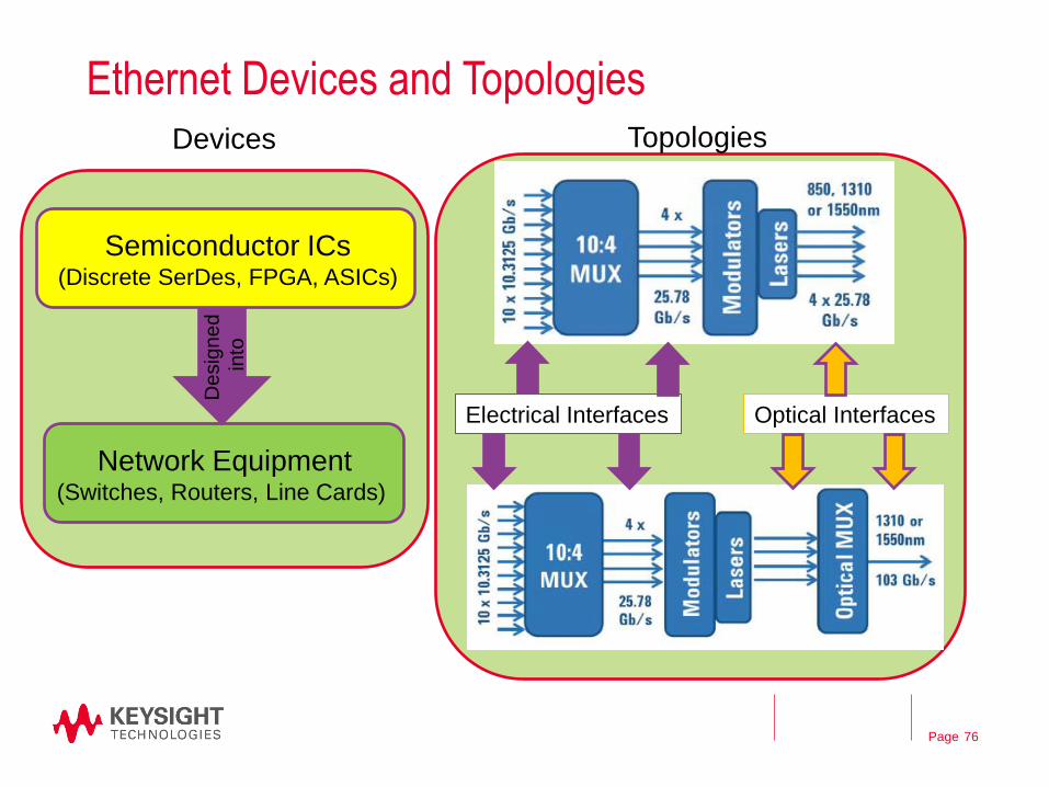
Ethernet Devices and Topologies
76
Electrical Interfaces Optical Interfaces
Semiconductor ICs (Discrete SerDes, FPGA, ASICs)
Network Equipment (Switches, Routers, Line Cards)
Devices
De
sig
ne
d
in
to
Topologies
Page
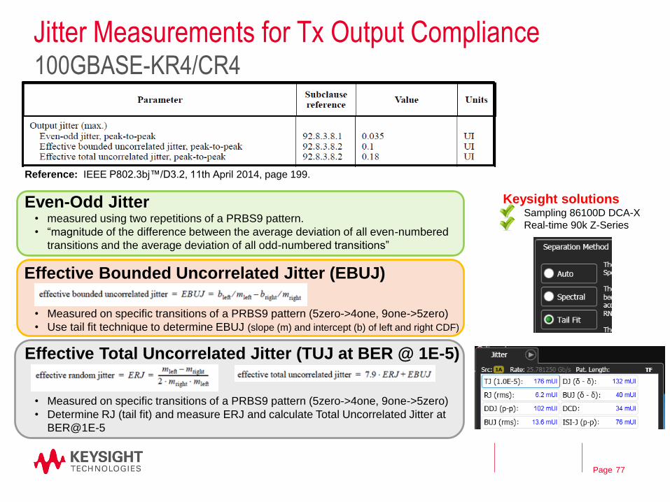
Jitter Measurements for Tx Output Compliance
Even-Odd Jitter
77
100GBASE-KR4/CR4
Effective Bounded Uncorrelated Jitter (EBUJ)
Effective Total Uncorrelated Jitter (TUJ at BER @ 1E-5)
• measured using two repetitions of a PRBS9 pattern.
• “magnitude of the difference between the average deviation of all even-numbered
transitions and the average deviation of all odd-numbered transitions”
• Measured on specific transitions of a PRBS9 pattern (5zero->4one, 9one->5zero)
• Use tail fit technique to determine EBUJ (slope (m) and intercept (b) of left and right CDF)
• Measured on specific transitions of a PRBS9 pattern (5zero->4one, 9one->5zero)
• Determine RJ (tail fit) and measure ERJ and calculate Total Uncorrelated Jitter at
BER@1E-5
Keysight solutions • Sampling 86100D DCA-X
• Real-time 90k Z-Series
Reference: IEEE P802.3bj™/D3.2, 11th April 2014, page 199.
Page
BERT Error
Detector
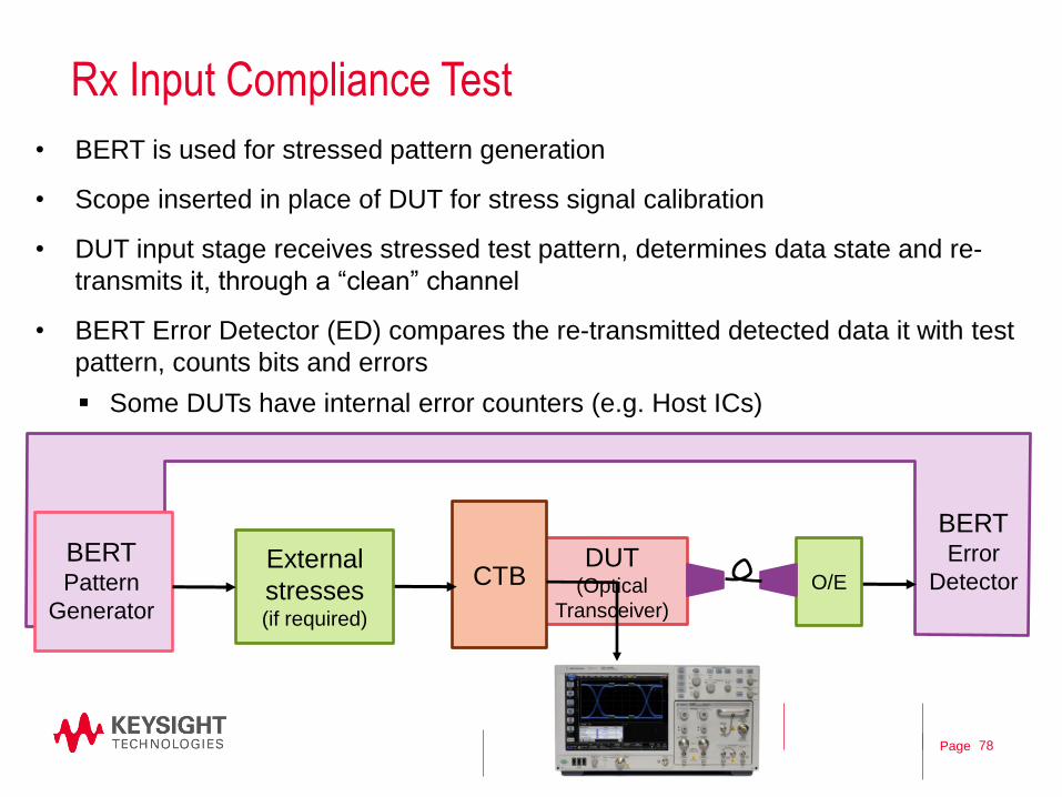
Rx Input Compliance Test
• BERT is used for stressed pattern generation
• Scope inserted in place of DUT for stress signal calibration
• DUT input stage receives stressed test pattern, determines data state and re-
transmits it, through a “clean” channel
• BERT Error Detector (ED) compares the re-transmitted detected data it with test
pattern, counts bits and errors
Some DUTs have internal error counters (e.g. Host ICs)
78
DUT (Optical
Transceiver)
O/E CTB BERT Pattern
Generator
External
stresses (if required)
Page
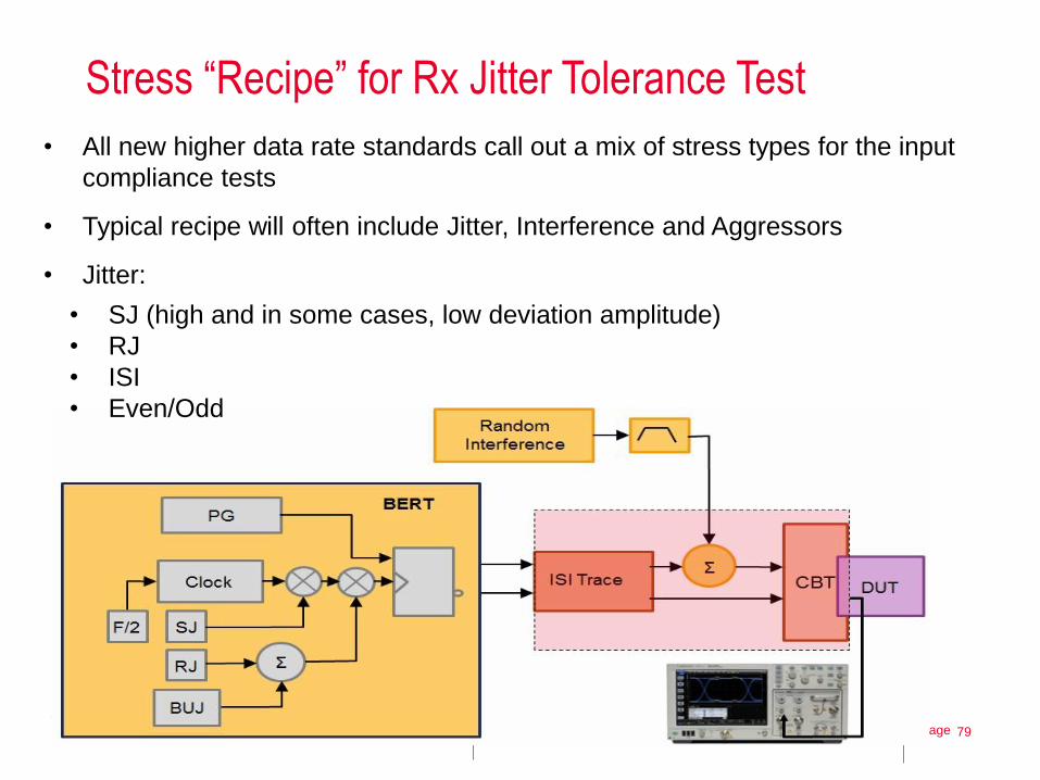
Stress “Recipe” for Rx Jitter Tolerance Test
79
• All new higher data rate standards call out a mix of stress types for the input
compliance tests
• Typical recipe will often include Jitter, Interference and Aggressors
• Jitter:
• SJ (high and in some cases, low deviation amplitude)
• RJ
• ISI
• Even/Odd
Page
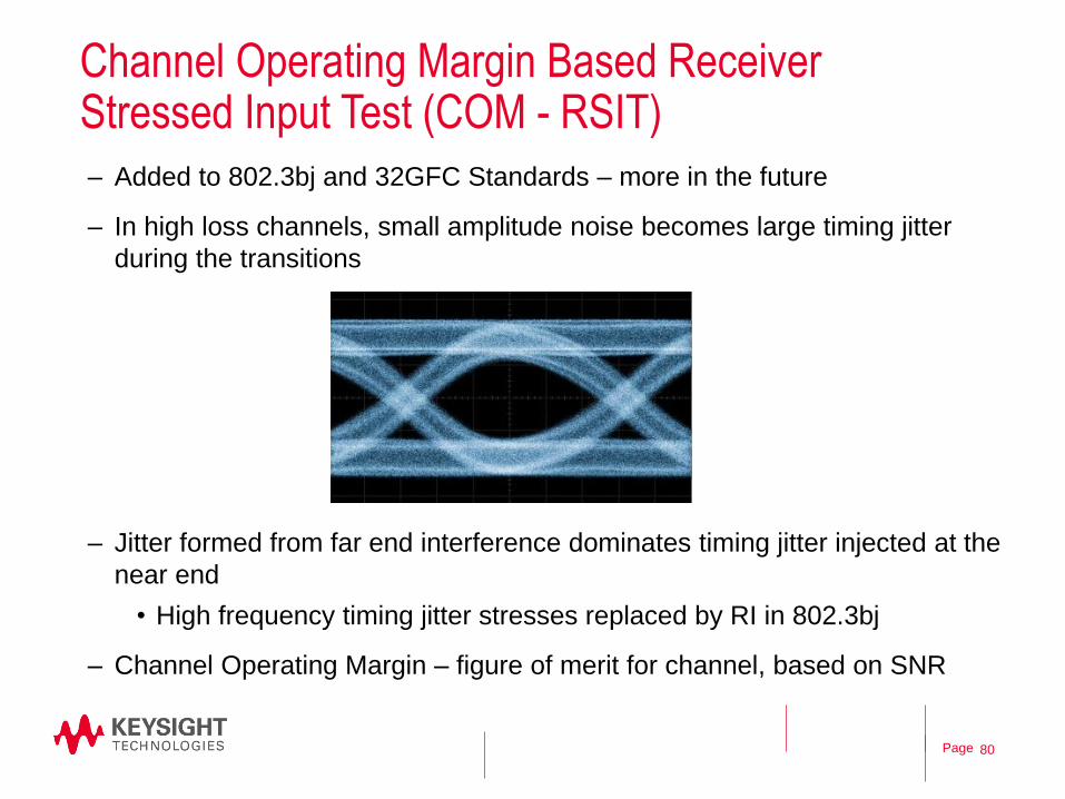
Channel Operating Margin Based Receiver Stressed Input Test (COM - RSIT)
– Added to 802.3bj and 32GFC Standards – more in the future
– In high loss channels, small amplitude noise becomes large timing jitter
during the transitions
– Jitter formed from far end interference dominates timing jitter injected at the
near end
• High frequency timing jitter stresses replaced by RI in 802.3bj
– Channel Operating Margin – figure of merit for channel, based on SNR
80
Page
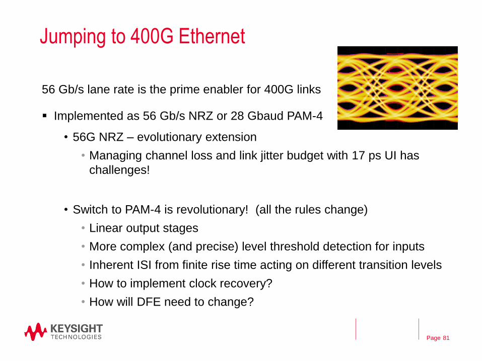
Jumping to 400G Ethernet
56 Gb/s lane rate is the prime enabler for 400G links
Implemented as 56 Gb/s NRZ or 28 Gbaud PAM-4
• 56G NRZ – evolutionary extension
• Managing channel loss and link jitter budget with 17 ps UI has
challenges!
• Switch to PAM-4 is revolutionary! (all the rules change)
• Linear output stages
• More complex (and precise) level threshold detection for inputs
• Inherent ISI from finite rise time acting on different transition levels
• How to implement clock recovery?
• How will DFE need to change?
81
Page
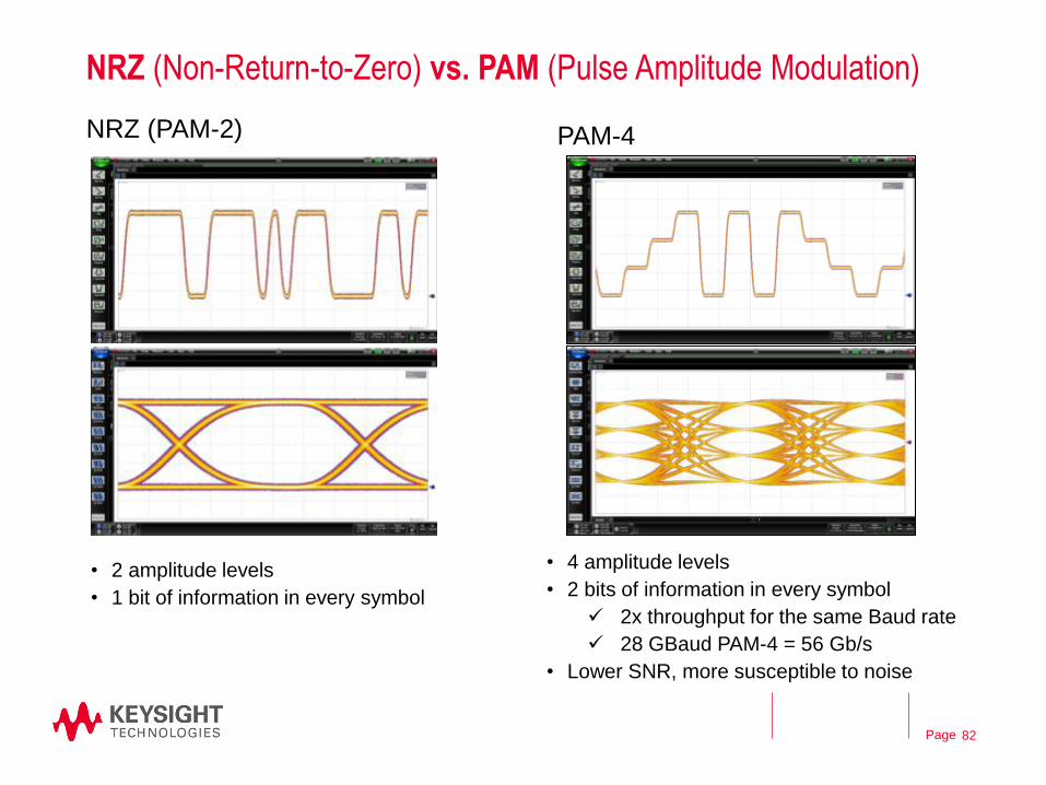
NRZ (Non-Return-to-Zero) vs. PAM (Pulse Amplitude Modulation)
NRZ (PAM-2)
82
PAM-4
• 2 amplitude levels
• 1 bit of information in every symbol
• 4 amplitude levels
• 2 bits of information in every symbol
2x throughput for the same Baud rate
28 GBaud PAM-4 = 56 Gb/s
• Lower SNR, more susceptible to noise
Page
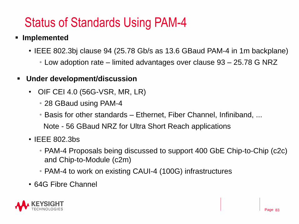
Status of Standards Using PAM-4
83
Implemented
• IEEE 802.3bj clause 94 (25.78 Gb/s as 13.6 GBaud PAM-4 in 1m backplane)
• Low adoption rate – limited advantages over clause 93 – 25.78 G NRZ
Under development/discussion
• OIF CEI 4.0 (56G-VSR, MR, LR)
• 28 GBaud using PAM-4
• Basis for other standards – Ethernet, Fiber Channel, Infiniband, ...
Note - 56 GBaud NRZ for Ultra Short Reach applications
• IEEE 802.3bs
• PAM-4 Proposals being discussed to support 400 GbE Chip-to-Chip (c2c)
and Chip-to-Module (c2m)
• PAM-4 to work on existing CAUI-4 (100G) infrastructures
• 64G Fibre Channel
Page 84
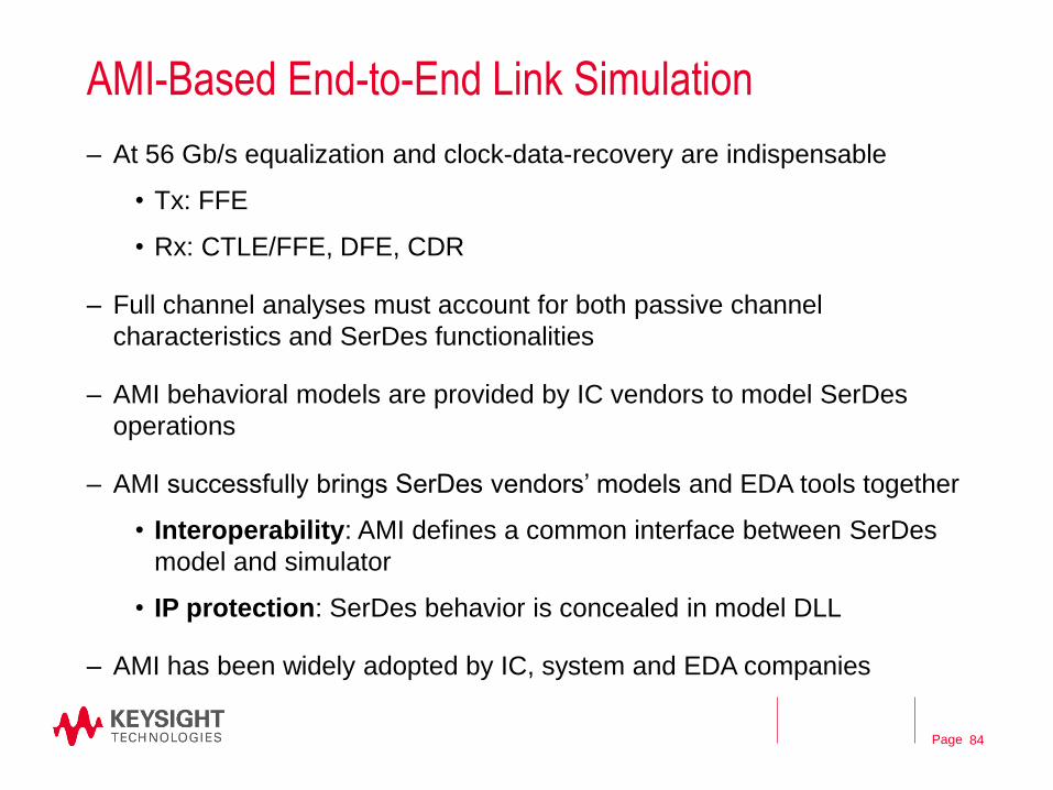
AMI-Based End-to-End Link Simulation
– At 56 Gb/s equalization and clock-data-recovery are indispensable
• Tx: FFE
• Rx: CTLE/FFE, DFE, CDR
– Full channel analyses must account for both passive channel
characteristics and SerDes functionalities
– AMI behavioral models are provided by IC vendors to model SerDes
operations
– AMI successfully brings SerDes vendors’ models and EDA tools together
• Interoperability: AMI defines a common interface between SerDes
model and simulator
• IP protection: SerDes behavior is concealed in model DLL
– AMI has been widely adopted by IC, system and EDA companies
Page 85
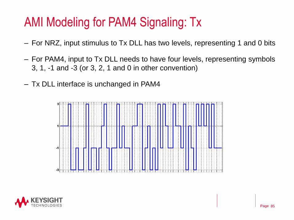
AMI Modeling for PAM4 Signaling: Tx
– For NRZ, input stimulus to Tx DLL has two levels, representing 1 and 0 bits
– For PAM4, input to Tx DLL needs to have four levels, representing symbols
3, 1, -1 and -3 (or 3, 2, 1 and 0 in other convention)
– Tx DLL interface is unchanged in PAM4
Page 86
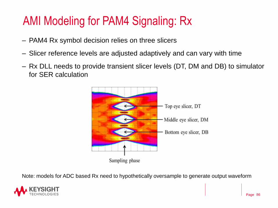
AMI Modeling for PAM4 Signaling: Rx
– PAM4 Rx symbol decision relies on three slicers
– Slicer reference levels are adjusted adaptively and can vary with time
– Rx DLL needs to provide transient slicer levels (DT, DM and DB) to simulator
for SER calculation
Note: models for ADC based Rx need to hypothetically oversample to generate output waveform
Page 87
AMI Simulation Flow for PAM4
Tx
DLL
Tx
analog channel
Rx
analog
Rx
DLL
clock times
DT
DM
DB
FFE Backplane
Board
Cable
Connector
Via
Package
…
AGC
CTLE/FFE
DFE
CDR
simulated by vendor supplied
AMI model DLL
simulated by EDA tool
Page 88
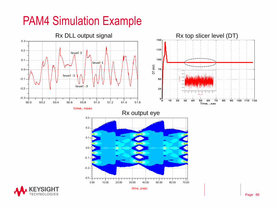
PAM4 Simulation Example Rx DLL output signal Rx top slicer level (DT)
Rx output eye
Page 89
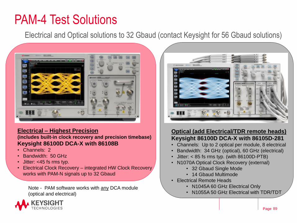
PAM-4 Test Solutions
Electrical – Highest Precision (includes built-in clock recovery and precision timebase)
Keysight 86100D DCA-X with 86108B • Channels: 2
• Bandwidth: 50 GHz
• Jitter: <45 fs rms typ.
• Electrical Clock Recovery – integrated HW Clock Recovery
works with PAM-N signals up to 32 Gbaud
Note - PAM software works with any DCA module
(optical and electrical)
Optical (add Electrical/TDR remote heads)
Keysight 86100D DCA-X with 86105D-281 • Channels: Up to 2 optical per module, 8 electrical
• Bandwidth: 34 GHz (optical), 60 GHz (electrical)
• Jitter: < 85 fs rms typ. (with 86100D-PTB)
• N1070A Optical Clock Recovery (external)
• 32 Gbaud Single Mode
• 14 Gbaud Multimode
• Electrical Remote Heads
• N1045A 60 GHz Electrical Only
• N1055A 50 GHz Electrical with TDR/TDT
Electrical and Optical solutions to 32 Gbaud (contact Keysight for 56 Gbaud solutions)
Page 90
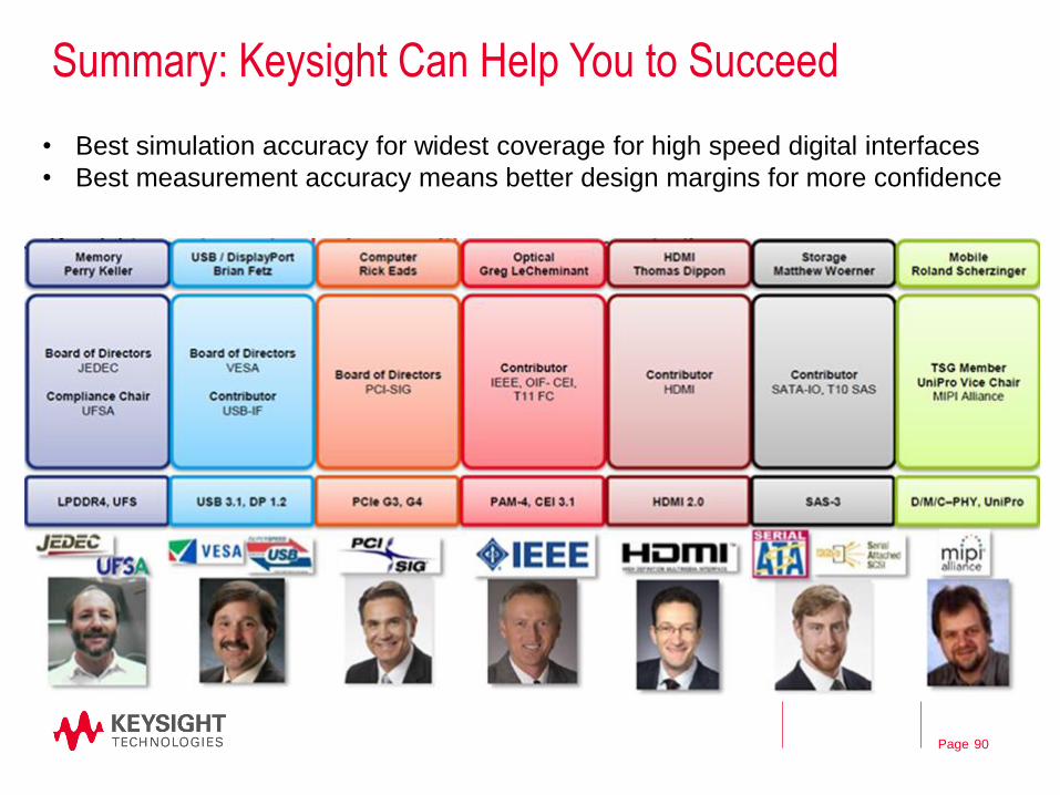
Summary: Keysight Can Help You to Succeed
• Best simulation accuracy for widest coverage for high speed digital interfaces
• Best measurement accuracy means better design margins for more confidence


