
February 2012
Figure 1. Typical Standby Application.
ORDERPART
NUMBER 85-265VAC
230 VAC or 115 VAC
w/Doubler
Product Highlights
Lowest Cost, Low Power Switcher Solution• LowercostthanRCC,discretePWMandotherintegrat-
ed/hybridsolutions• Costeffectivereplacementforbulkylinearadapters• Lowestcomponentcount• SimpleON/OFFcontrol–noloopcompensationdevices• Nobiaswinding–simpler,lowercosttransformer• AllowssimpleRCtypeEMIfilterforupto2Wfrom
universalinputor4Wfrom115VACinput Extremely Energy Efficient • Consumesonly30/60mWat115/230VACwithnoload• MeetsBlueAngel,EnergyStar,Energy2000and200mW
Europeancellphonerequirementsforstandby• Saves$1to$4peryearinenergycosts(at$0.12/kWHr)
comparedtobulkylinearadapters• Idealforcellularphonechargers,standbypowersuppliesfor
PC,TVandVCR,utilitymeters,andcordlessphones.
High Performance at Low Cost• High-voltagepowered–idealforchargerapplications• Veryhighloopbandwidthprovidesexcellenttransient
responseandfastturnonwithpracticallynoovershoot• Currentlimitoperationrejectslinefrequencyripple• Glitchfreeoutputwheninputisremoved• Built-incurrentlimitandthermalprotection• 44kHzoperation(TNY253/4)withsnubberclamp
reducesEMIandvideonoiseinTVsandVCRs• Operateswithoptocouplerorbiaswindingfeedback
Description
TheTinySwitchfamilyusesabreakthroughdesigntoprovidethelowestcost,highefficiency,off-lineswitchersolutioninthe0to10Wrange.Thesedevicesintegratea700VpowerMOSFET, oscillator, high-voltage switched current source,current limitand thermalshutdowncircuitry. Theystart-upandrunonpowerderivedfromtheDRAINvoltage,eliminat-ingtheneedforatransformerbiaswindingandtheassociatedcircuitry.Andyet,theyconsumeonlyabout80mWatnoload,from265VACinput.AsimpleON/OFFcontrolschemealsoeliminatestheneedforloopcompensation.
TNY253P
TNY254P
TinySwitch Selection Guide
PACKAGE
DIP-8
DIP-8
SMD-8
SMD-8
TNY253G
TNY255P
0-2 W
1-4 W
0-4 W
2-5 W
TNY255G
DIP-8
TNY254G
SMD-83.5-6.5 W4-10 W
TheTNY253andTNY254switchat44kHztominimizeEMIand toallowasimplesnubberclampto limitDRAINspikevoltage.Atthesametime,theyallowuseoflowcostEE16coretransformerstodeliverupto5W.TheTNY253isidenticaltoTNY254exceptforitslowercurrentlimit,whichreducesoutputshort-circuit current for applications under 2.5W.TNY255useshigherswitchingrateof130kHztodeliverupto10WfromthesamelowcostEE16coreforapplicationssuchasPCstandbysupply. AnEE13orEF13corewith safety spacedbobbincanbeusedforapplicationsunder2.5W.Absenceofabiaswindingeliminatestheneedfortaping/marginsinmostapplications,whentripleinsulatedwireisusedforthesecondary.Thissimplifiesthetransformerconstructionandreducescost.
PI-2178-022699
Wide-RangeHigh-Voltage
DC Input
TinySwitchD
S
EN
BP
+
–
+
–
DCOutput
Table 1. *Please refer to the Key Application Considerations section for details.
Recommended Range for Lowest System Cost*
TNY253/254/255TinySwitch™ FamilyEnergy Efficient, Low Power Off-line Switchers
Rev E 02/12
TNY253/254/255
2
Figure 2. Functional Block Diagram.
Figure 3. Pin Configuration.
Pin Functional Description
DRAIN (D) Pin:PowerMOSFETdrainconnection.Providesinternaloperatingcurrentforbothstart-upandsteady-stateoperation.
BYPASS (BP) Pin:Connectionpointforanexternalbypasscapacitorfortheinter-nallygenerated5.8Vsupply.Bypasspinisnotintendedforsourcingsupplycurrenttoexternalcircuitry.
ENABLE (EN) Pin:ThepowerMOSFETswitchingcanbeterminatedbypullingthispinlow.TheI-Vcharacteristicofthispinisequivalenttoavoltagesourceofapproximately1.5Vwithasourcecurrentclampof50µA.
SOURCE (S) Pin:PowerMOSFETsourceconnection.Primaryreturn.
TinySwitch Functional Description
TinySwitchisintendedforlowpoweroff-lineapplications.Itcombinesahigh-voltagepowerMOSFETswitchwithapowersupplycontrollerinonedevice.UnlikeaconventionalPWM(PulseWidthModulator) controller, the TinySwitch uses asimpleON/OFFcontroltoregulatetheoutputvoltage.
TheTinySwitch controller consists of an Oscillator, Enable(SenseandLogic)circuit,5.8VRegulator,Undervoltagecircuit,
HystereticOverTemperatureProtection,CurrentLimitcircuit,LeadingEdgeBlanking,anda700VpowerMOSFET.Figure2showsafunctionalblockdiagramwiththemostimportantfeatures.
OscillatorTheoscillatorfrequencyisinternallysetat44kHz(130kHzfortheTNY255).ThetwosignalsofinterestaretheMaxi-mumDutyCyclesignal(DMAX)whichrunsattypically67%dutycycleandtheClocksignalthatindicatesthebeginningofeachcycle.Whencyclesareskipped(seebelow),theoscilla-torfrequencydoubles(exceptforTNY255whichremainsat130kHz).ThisincreasesthesamplingrateattheENABLEpinforfasterloopresponse.
Enable (Sense and Logic)TheENABLEpincircuithasasourcefollowerinputstagesetat1.5V.Theinputcurrentisclampedbyacurrentsourcesetat50µAwith10µAhysteresis.Theoutputoftheenablesense
PI-2197-061898
CLOCK
OSCILLATOR5.8 V5.1 V
SOURCE
S
R
Q
DCMAX
BYPASS
+
- VILIMIT
LEADINGEDGE
BLANKING
THERMALSHUTDOWN
+
-
DRAINREGULATOR5.8 V
UNDERVOLTAGE
1.5 V + VTH
ENABLE
Q
50 μA
PI-2199-031501
ENABLE
8
5
7
6
DRAIN
SOURCE
SOURCE
SOURCE
1
4
2
3
SOURCE
SOURCEBYPASS
P Package (DIP-8) G Package (SMD-8)
TNY253/254/255
3Rev E02/12
circuit is sampledat the rising edgeof theoscillatorClocksignal(atthebeginningofeachcycle).Ifitishigh,thenthepowerMOSFETisturnedon(enabled)forthatcycle,otherwisethepowerMOSFETremainsintheoffstate(cycleskipped).Sincethesamplingisdoneonlyonceatthebeginningofeachcycle,anysubsequentchangesattheENABLEpinduringthecycleareignored.
5.8 V RegulatorThe5.8VregulatorchargesthebypasscapacitorconnectedtotheBYPASSpinto5.8VbydrawingacurrentfromthevoltageontheDRAIN,whenevertheMOSFETisoff.TheBYPASSpinistheinternalsupplyvoltagenodefortheTinySwitch.WhentheMOSFETison,theTinySwitchrunsoffoftheenergystoredinthebypasscapacitor.ExtremelylowpowerconsumptionoftheinternalcircuitryallowstheTinySwitchtooperatecontinu-ouslyfromthecurrentdrawnfromtheDRAINpin.Abypasscapacitorvalueof0.1µFissufficientforbothhighfrequencyde-couplingandenergystorage.
UndervoltageTheundervoltagecircuitrydisablesthepowerMOSFETwhentheBYPASSpinvoltagedropsbelow5.1V.OncetheBYPASSpinvoltagedropsbelow5.1V,ithastorisebackto5.8Vtoenable(turn-on)thepowerMOSFET.
Hysteretic Over Temperature ProtectionThethermalshutdowncircuitrysensesthediejunctiontem-perature.Thethresholdissetat135°Cwith70°Chysteresis.When the junction temperature rises above this threshold(135°C)thepowerMOSFETisdisabledandremainsdisableduntilthediejunctiontemperaturefallsby70°C,atwhichpointitisre-enabled.
Current LimitThe current limit circuit senses the current in the powerMOSFET.Whenthiscurrentexceedstheinternalthreshold(ILIMIT),thepowerMOSFETisturnedofffortheremainderofthatcycle.
The leading edge blanking circuit inhibits the current limitcomparatorforashort time(tLEB)after thepowerMOSFETisturnedon.Thisleadingedgeblankingtimehasbeensetsothat current spikes caused by primary-side capacitance andsecondary-siderectifierreverserecoverytimewillnotcauseprematureterminationoftheswitchingpulse.
TinySwitch Operation
TinySwitchisintendedtooperateinthecurrentlimitmode.Whenenabled,theoscillatorturnsthepowerMOSFETonatthebeginningofeachcycle.TheMOSFETisturnedoffwhenthecurrentrampsuptothecurrentlimit.Themaximumon-timeoftheMOSFETislimitedtoDCMAXbytheoscillator.SincethecurrentlimitandfrequencyofagivenTinySwitchdevice
areconstant,thepowerdeliveredisproportionaltotheprimaryinductanceofthetransformerandisrelativelyindependentoftheinputvoltage.Therefore,thedesignofthepowersupplyinvolvescalculatingtheprimaryinductanceofthetransformerforthemaximumpowerrequired.AslongastheTinySwitchdevicechosenisratedforthepowerlevelatthelowestinputvoltage,thecalculatedinductancewillrampupthecurrenttothecurrentlimitbeforetheDCMAXlimitisreached.
Enable FunctionTheTinySwitchsensestheENABLEpintodeterminewhetherornottoproceedwiththenextswitchcycleasdescribedearlier.OnceacycleisstartedTinySwitchalwayscompletesthecycle(evenwhentheENABLEpinchangesstatehalfwaythroughthecycle).Thisoperationresultsinapowersupplywhoseoutputvoltagerippleisdeterminedbytheoutputcapacitor,amountofenergyperswitchcycleandthedelayoftheENABLEfeedback.
TheENABLEsignalisgeneratedonthesecondarybycomparingthepowersupplyoutputvoltagewithareferencevoltage.TheENABLEsignalishighwhenthepowersupplyoutputvoltageislessthanthereferencevoltage.
In a typical implementation, theENABLEpin is driven byanoptocoupler.ThecollectoroftheoptocouplertransistorisconnectedtotheENABLEpinandtheemitterisconnectedtotheSOURCEpin.TheoptocouplerLEDisconnectedinserieswith aZener across theDCoutput voltage to be regulated.Whentheoutputvoltageexceedsthetargetregulationvoltagelevel(optocouplerdiodevoltagedropplusZenervoltage),theoptocouplerdiodewillstarttoconduct,pullingtheENABLEpinlow.TheZenercouldbereplacedbyaTL431deviceforimprovedaccuracy.
TheENABLEpinpull-downcurrent threshold isnominally50µA,butissetto40µAtheinstantthethresholdisexceeded.Thisisresetto50µAwhentheENABLEpull-downcurrentdropsbelowthecurrentthresholdof40µA.
ON/OFF ControlTheinternalclockoftheTinySwitchrunsallthetime.Atthebeginning of each clock cycle the TinySwitch samples theENABLEpintodecidewhetherornottoimplementaswitchcycle.IftheENABLEpinishigh(<40µA),thenaswitchingcycle takesplace. If theENABLEpin is low (greater than50µA)thennoswitchingcycleoccurs,andtheENABLEpinstatusissampledagainatthestartofthesubsequentclockcycle.
At full loadTinySwitchwillconductduring themajorityofitsclockcycles(Figure4). At loads less thanfull load, theTinySwitchwill“skip”morecyclesinordertomaintainvolt-age regulation at the secondary output (Figure 5). At lightloadornoload,almostallcycleswillbeskipped(Figure6).Asmallpercentageofcycleswillconducttosupportthepowerconsumptionofthepowersupply.

Rev E 02/12
TNY253/254/255
4
Figure 4. TinySwitch Operation at Heavy Load. Figure 5. TinySwitch Operation at Medium Load.
V
DRAINV
EN
CLOCK
DC
DRAINI
MAX
PI-2255-061298
V
DRAINV
EN
CLOCK
DC
DRAINI
MAX
PI-2259-061298
TheresponsetimeofTinySwitchON/OFFcontrolschemeisveryfastcomparedtonormalPWMcontrol.Thisprovideshighlineripplerejectionandexcellenttransientresponse.
Power Up/DownTinySwitchrequiresonlya0.1µFcapacitorontheBYPASSpin.Becauseofthesmallsizeofthiscapacitor,thepower-updelayiskepttoanabsoluteminimum,typically0.3ms(Fig-ure7).DuetothefastnatureoftheON/OFFfeedback,thereisnoovershootatthepowersupplyoutput.Duringpower-down,thepowerMOSFETwillswitchuntiltherectifiedlinevoltagedropstoapproximately12V.ThepowerMOSFETwillthenremainoffwithoutanyglitches(Figure8).
Bias Winding EliminatedTinySwitchdoesnotrequireabiaswindingtoprovidepowerto the chip. Instead it draws the power directly from theDRAINpin(seeFunctionalDescriptionabove).Thishastwomainbenefits.Firstforanominalapplication,thiseliminatesthecostofanextrabiaswindingandassociatedcomponents.Secondly,forchargerapplications, thecurrent-voltagechar-acteristicoftenallowstheoutputvoltagetofalltolowvalueswhilestilldeliveringpower.Thistypeofapplicationnormallyrequiresaforward-biaswindingwhichhasmanymoreassoci-atedcomponents,noneofwhicharenecessarywithTinySwitch.
Current Limit OperationEachswitchingcycleisterminatedwhentheDRAIN currentreachesthecurrentlimitoftheTinySwitch.Foragivenprimaryinductanceandinputvoltage,thedutycycleisconstant.How-ever,dutycycledoeschangeinverselywiththeinputvoltageproviding“voltagefeed-forward”advantages:goodlineripple
rejectionandrelativelyconstantpowerdeliveryindependentoftheinputvoltage.
44 kHz Switching Frequency (TNY253/254)Switchingfrequency(withnocycleskipping)issetat44kHz.Thisprovidesseveraladvantages.Athigherswitchingfrequen-cies,thecapacitiveswitchinglossesareasignificantproportionofthepowerlossesinapowersupply.Athigherfrequencies,thepreferredsnubbingschemesareRCDordiode-Zenerclamps.However,duetothelowerswitchingfrequencyofTinySwitch,itispossibletouseasimpleRCsnubber(andevenjustacapaci-toralonein115VACapplicationsatpowerslevelsbelow4W).
Secondly,alowswitchingfrequencyalsoreducesEMIfilteringrequirements.At44kHz,thefirst,secondandthirdharmon-icsareallbelow150kHzwheretheEMIlimitsarenotveryrestrictive.Forpowerlevelsbelow4WitispossibletomeetworldwideEMIrequirementswithonlyresistiveandcapaci-tivefilterelements(noinductorsorchokes).ThissignificantlyreducesEMIfiltercosts.
Finally, if the application requires stringent noise emissions(suchasvideoapplications),thentheTNY253/254willallowmore effective use of diode snubbing (and other secondarysnubbingtechniques).ThelowerswitchingfrequencyallowsRCsnubberstobeusedtoreducenoise,withoutsignificantlyimpactingtheefficiencyofthesupply.
130 kHz Switching Frequency (TNY255)The switching frequency (with no cycle skipping) is set at130kHz.ThisallowstheTNY255todeliver10Wwhilestillusingthesamesize,lowcosttransformer(EE16)asusedbytheTNY253/254forlowerpowerapplications.

TNY253/254/255
5Rev E02/12
Figure 6. TinySwitch Operation at Light Load.
Figure 7. TinySwitch Power-Up Timing Diagram.
Figure 8. TinySwitch Power Down Timing Diagram.
PI-2261-061198
V
DRAINV
EN
CLOCK
DC
DRAINI
MAX
BYPASS Pin CapacitorTheBYPASSpinusesasmall0.1µFceramiccapacitorfordecouplingtheinternalpowersupplyoftheTinySwitch.
Application Examples
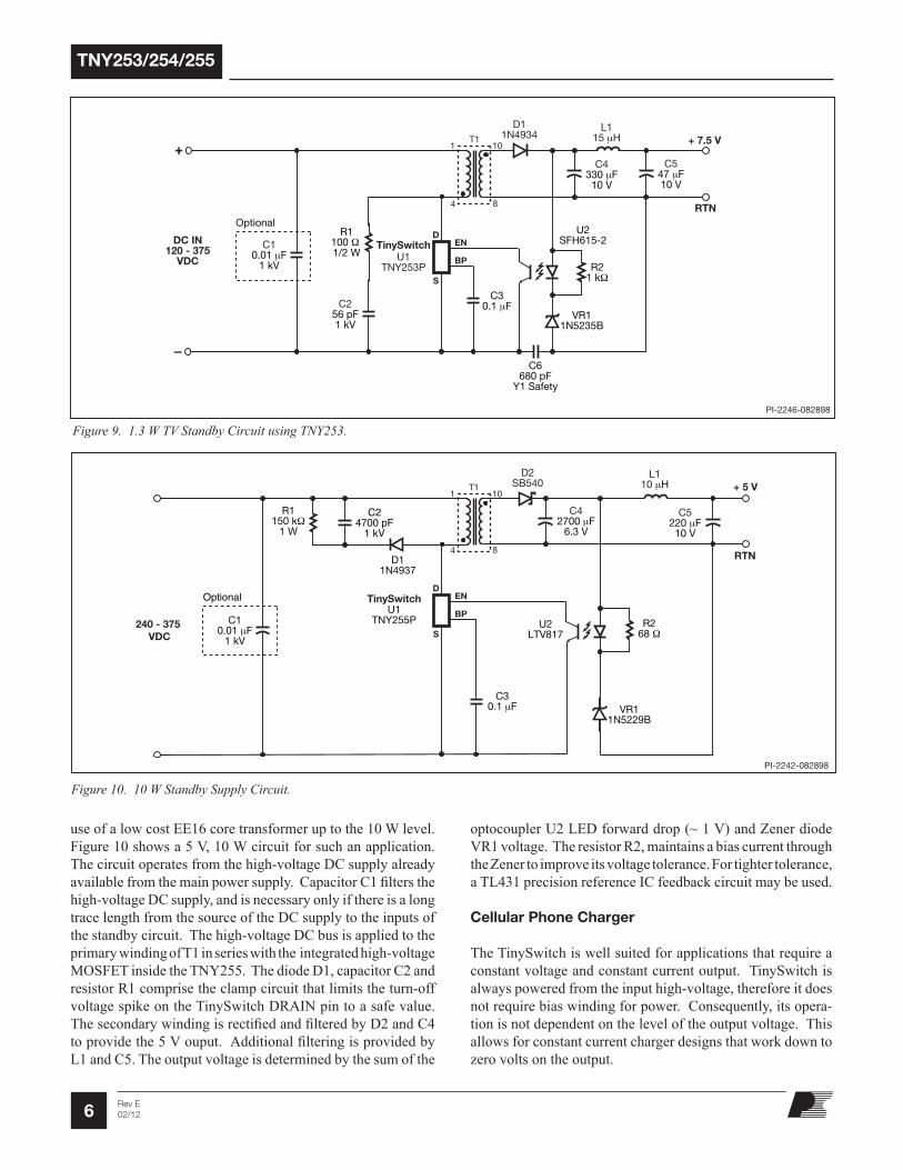
Television Standby
TinySwitchisanidealsolutionforlowcost,highefficiencystandbypowersuppliesusedinconsumerelectronicproductssuchasTVs.Figure9showsa7.5V,1.3WflybackcircuitthatusesTNY253forimplementingaTVstandbysupply.ThecircuitoperatesfromtheDChigh-voltagealreadyavailablefromthemainpowersupply.Thisinputvoltagecanrangefrom120to375VDCdependingontheinputACvoltagerangethattheTVisratedfor.CapacitorC1filtersthehigh-voltageDCsupply,andisnecessaryonlyifthereisalongtracelengthfromthesourceoftheDCsupplytotheinputsoftheTVstandbycircuit.Thehigh-voltageDCbusisappliedtotheseriescombinationoftheprimarywindingofT1andtheintegratedhigh-voltageMOSFETinsidetheTNY253.ThelowoperatingfrequencyoftheTNY253(44kHz),allowsalowcostsnubbercircuitC2andR1tobeusedinplaceofaprimaryclampcircuit.InadditiontolimitingtheDRAINturnoffvoltagespiketoasafevalue,theRCsnubberalsoreducesradiatedvideonoisebyloweringthedv/dtoftheDRAINwaveform,whichiscriticalforvideoapplicationssuchasTVandVCR.OnfixedfrequencyPWMandRCCcircuits,useofasnubberwillresultinanundesir-ablefixedACswitchinglossthatisindependentofload.TheON/OFFcontrolontheTinySwitcheliminatesthisproblemby scaling the effective switching frequency and therefore,
switchinglosslinearlywithload.Thustheefficiencyofthesupplystaysrelativelyconstantdowntoafractionofawattofoutputloading.
ThesecondarywindingisrectifiedandfilteredbyD1andC4tocreatethe7.5Voutput.L1andC5provideadditionalfiltering.TheoutputvoltageisdeterminedbythesumoftheoptocouplerU2LEDforwarddrop(~1V)andZenerdiodeVR1voltage.TheresistorR2,maintainsabiascurrentthroughtheZenertoimproveitsvoltagetolerance.
10 W Standby
TheTNY255isidealforstandbyapplicationsthatrequireupto10Wofpowerfrom230VACor100/115VACwithdoublercircuit.TheTNY255operatesat130kHzasopposedto44kHzforTNY253/254.Thehigherfrequencyoperationallowsthe
V
DRAINV
IN
PI–
2253
-062
398
0 .2
Time (ms).4 .6 .8 1
0 V
0 V
V
DRAINV
IN
12 V
PI–
2251
-062
398
12 V
0 100
Time (ms)200 300 400 500
0 V
0 V
Rev E 02/12
TNY253/254/255
6
Figure 9. 1.3 W TV Standby Circuit using TNY253.
Figure 10. 10 W Standby Supply Circuit.
useofalowcostEE16coretransformeruptothe10Wlevel.Figure10showsa5V,10Wcircuitforsuchanapplication.Thecircuitoperatesfromthehigh-voltageDCsupplyalreadyavailablefromthemainpowersupply.CapacitorC1filtersthehigh-voltageDCsupply,andisnecessaryonlyifthereisalongtracelengthfromthesourceoftheDCsupplytotheinputsofthestandbycircuit.Thehigh-voltageDCbusisappliedtotheprimarywindingofT1inserieswiththeintegratedhigh-voltageMOSFETinsidetheTNY255.ThediodeD1,capacitorC2andresistorR1comprisetheclampcircuitthatlimitstheturn-offvoltagespikeontheTinySwitchDRAINpintoasafevalue.ThesecondarywindingisrectifiedandfilteredbyD2andC4toprovidethe5Vouput.AdditionalfilteringisprovidedbyL1andC5.Theoutputvoltageisdeterminedbythesumofthe
optocouplerU2LEDforwarddrop(~1V)andZenerdiodeVR1voltage.TheresistorR2,maintainsabiascurrentthroughtheZenertoimproveitsvoltagetolerance.Fortightertolerance,aTL431precisionreferenceICfeedbackcircuitmaybeused.
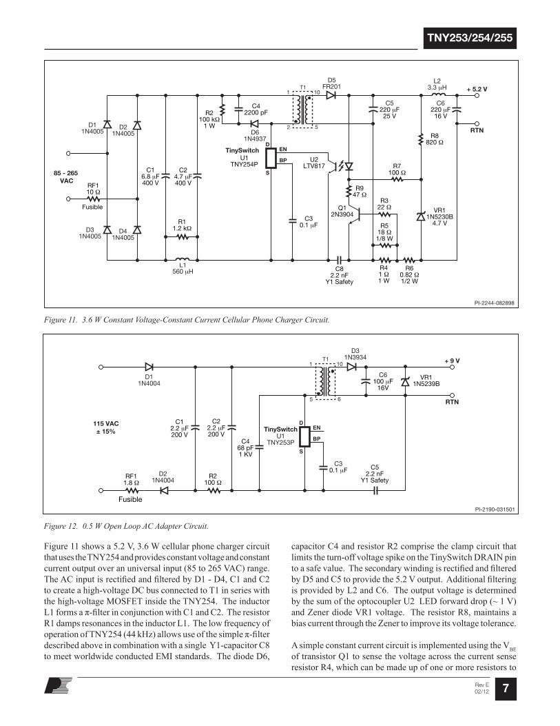
Cellular Phone Charger
TheTinySwitchiswellsuitedforapplicationsthatrequireaconstantvoltageandconstantcurrentoutput.TinySwitchisalwayspoweredfromtheinputhigh-voltage,thereforeitdoesnotrequirebiaswindingforpower.Consequently,itsopera-tionisnotdependentontheleveloftheoutputvoltage.Thisallowsforconstantcurrentchargerdesignsthatworkdowntozerovoltsontheoutput.
PI-2242-082898
TinySwitchD
S
EN
BP
+ 5 V
RTN
C10.01 μF
1 kV
C30.1 μF
240 - 375 VDC
R1150 kΩ
1 W
U2LTV817
D2SB540
L110 μH
C42700 μF
6.3 V
C5220 μF10 V
VR11N5229B
U1TNY255P
C24700 pF
1 kV
T11
4 8
10
R268 Ω
D11N4937
Optional
PI-2246-082898
DC IN120 - 375
VDC
TinySwitchD
S
EN
BP
+
–
+ 7.5 V
RTN
C30.1 μF
R21 kΩ
VR11N5235B
C10.01 μF
1 kV
R1100 Ω 1/2 W
C256 pF1 kV
D11N4934
L115 μH
C547 μF10 V
C4330 μF10 V
U1TNY253P
T1
U2SFH615-2
C6680 pF
Y1 Safety
1
4 8
10
Optional
TNY253/254/255
7Rev E02/12
Figure 11. 3.6 W Constant Voltage-Constant Current Cellular Phone Charger Circuit.
Figure11showsa5.2V,3.6WcellularphonechargercircuitthatusestheTNY254andprovidesconstantvoltageandconstantcurrentoutputoveranuniversalinput(85to265VAC)range.TheACinputisrectifiedandfilteredbyD1-D4,C1andC2tocreateahigh-voltageDCbusconnectedtoT1inserieswiththehigh-voltageMOSFETinsidetheTNY254.TheinductorL1formsaπ-filterinconjunctionwithC1andC2.TheresistorR1dampsresonancesintheinductorL1.ThelowfrequencyofoperationofTNY254(44kHz)allowsuseofthesimpleπ-filterdescribedaboveincombinationwithasingleY1-capacitorC8tomeetworldwideconductedEMIstandards.ThediodeD6,
capacitorC4andresistorR2comprisetheclampcircuitthatlimitstheturn-offvoltagespikeontheTinySwitchDRAINpintoasafevalue.ThesecondarywindingisrectifiedandfilteredbyD5andC5toprovidethe5.2Voutput.AdditionalfilteringisprovidedbyL2andC6.TheoutputvoltageisdeterminedbythesumoftheoptocouplerU2LEDforwarddrop(~1V)andZenerdiodeVR1voltage.TheresistorR8,maintainsabiascurrentthroughtheZenertoimproveitsvoltagetolerance.
AsimpleconstantcurrentcircuitisimplementedusingtheVBEoftransistorQ1tosensethevoltageacrossthecurrentsenseresistorR4,whichcanbemadeupofoneormoreresistorsto
Figure 12. 0.5 W Open Loop AC Adapter Circuit.
PI-2244-082898
TinySwitchD
S
EN
BP
+ 5.2 V
RTND1
1N4005
C16.8 μF400 V
Fusible
RF110 Ω
C30.1 μF
85 - 265 VAC
L1560 μH
D21N4005
D31N4005
D41N4005
R2100 kΩ
1 W
U2LTV817
D5FR201
L23.3 μH
C5220 μF25 V
C24.7 μF400 V
C6220 μF16 V
R7100 Ω
R322 Ω
R41 Ω1 W
R947 Ω
Q12N3904
R8820 Ω
VR11N5230B
4.7 V
C82.2 nF
Y1 Safety
U1TNY254P
C42200 pF
D61N4937
R60.82 Ω1/2 W
T1
R11.2 kΩ
1
2 5
10
R518 Ω1/8 W
PI-2190-031501
TinySwitchD
S
EN
BP
+ 9 V
RTN
D11N4004
C12.2 μF200 V
Fusible
RF11.8 Ω
C468 pF1 KV
115 VAC± 15%
R2100 Ω
D21N4004
C30.1 μF
D31N3934
C6100 μF
16V
C22.2 μF200 V
VR11N5239B
C52.2 nF
Y1 Safety
U1TNY253P
T11
5 6
10
Rev E 02/12
TNY253/254/255
8
achieve theappropriatevalue. R3 isabasecurrent limitingresistor.WhenthedropacrossR4exceedstheVBEoftransistorQ1,itturnsonandtakesoverthecontroloftheloopbydrivingtheoptocouplerLED.R6dropsanadditionalvoltagetokeepthecontrolloopinoperationdowntozerovoltsontheoutput.Withtheoutputshorted,thedropacrossR4andR6(~1.5V)issufficienttokeeptheQ1andLEDcircuitactive.ResistorsR7andR9limittheforwardcurrentthatcouldbedrawnthroughVR1byQ1underoutputshort-circuitconditions,due to thevoltagedropacrossR6andR4.
AC Adapter
Manyconsumerelectronicproductsutilizelowpower50/60HztransformerbasedACadapters.TheTinySwitchcancostef-fectivelyreplace these linearadapterswithasolution that islighter,smallerandmoreenergyefficient.Figure12showsa9V,0.5WACadaptercircuitusingtheTNY253.Thiscircuitoperatesfroma115VACinput.Tosavecost,thiscircuitrunswithout any feedback, in discontinuous conductionmode todeliver constant power output relatively independent of in-putvoltage.TheoutputvoltageisdeterminedbythevoltagedropacrossZenerdiodeVR1.Theprimaryinductanceofthetransformerischosentodeliverapowerthatisinexcessoftherequiredoutputpowerbyatleast50%toallowforcomponenttolerancesandtomaintainsomecurrentthroughtheZenerVR1atfullload.Atnoload,allofthepowerisdeliveredtotheZenerwhichshouldberatedandheatsinkedaccordingly.Inspiteofaconstantpowerconsumptionfromthemainsinput,thissolu-tionisstillsignificantlymoreefficientthanlinearadaptersuptooutputpowerlevelsofapproximately1W.
TheACinputisrectifiedbydiodesD1andD2.D2isusedtoreduceconductedEMIbyonlyallowingnoiseontotheneutrallineduringdiodeconduction.TherectifiedACisthenfilteredbycapacitorsC1andC2togenerateahigh-voltageDCbus,whichisappliedtotheseriescombinationoftheprimarywind-ingofT1andthehigh-voltageMOSFETinsidetheTNY253.TheresistorR2alongwithcapacitorsC1andC2formaπ-filterwhich is sufficient formeetingEMIconducted emissions atthesepowerlevels.C5isaYcapacitorwhichisusedtoreducecommonmodeEMI.Duetothe700VratingoftheTinySwitchMOSFET,asimplecapacitivesnubber(C4)isadequatetolimittheleakageinductancespikein115VACapplications,atlowpowerlevels.ThesecondarywindingisrectifiedandfilteredbyD3andC6.
Key Application Considerations
For the most up to date information visit our Web site at: www.powerint.com
Design
Output Power RangeThepowerlevelsshownintheTinySwitchSelectionGuide(Table1)areapproximate,recommendedoutputpowerrangesthat will provide a cost optimum design and are based onfollowingassumptions:
1. TheminimumDCinputvoltageis90Vorhigherfor85VACinputor240Vorhigherfor230VACinputor115VACinputwithavoltagedoubler.
2. The TinySwitch is not thermally limited - the sourcepinsaresolderedtosufficientcopperareatokeepthedietemperatureatorbelow100°C.ThislimitationdoesnotusuallyapplytoTNY253andTNY254.
ThemaximumpowercapabilityofaTinySwitchdependsonthe thermal environment, transformer core size and design(continuousordiscontinuous),efficiencyrequired,minimumspecifiedinputvoltage,inputstoragecapacitance,outputvolt-age,outputdiodeforwarddrop,etc.,andcanbedifferentfromthevaluesshownintheselectionguide.
Audible Noise Atloadsotherthanmaximumload,thecycleskippingmodeoperationused inTinySwitchcangenerateaudiofrequencycomponentsinthetransformer.Thiscancausethetransformerto produce audio noise. Transformer audible noise can bereduced by utilizing appropriate transformer constructiontechniquesanddecreasing thepeakfluxdensity. Formoreinformation on audio suppression techniques, please checkthe Application Notes section on our Web site atwww.powerint.com.
CeramiccapacitorsthatusedielectricssuchasZ5U,whenusedinclampandsnubbercircuits,canalsogenerateaudionoiseduetoelectrostrictionandpiezo-electriceffects.Ifthisisthecase,replacingthemwithacapacitorhavingadifferenttypeofdielectricisthesimplestsolution.Polyesterfilmcapacitorisagoodalternative.
Short-Circuit CurrentTheTinySwitchdoesnothaveanauto-restartfeature.Asaresult,TinySwitchwillcontinuetodeliverpowertotheloadduringoutputshort-circuitconditions.Intheworstcase,peakshort-circuitcurrentisequaltotheprimarycurrentlimit(ILIMIT)multipliedbytheturnsratioofthetransformer(Np/Ns).Inatypicaldesigntheaveragecurrentis25to50%lowerthanthis peakvalue. At the power levels ofTinySwitch this is
TNY253/254/255
9Rev E02/12
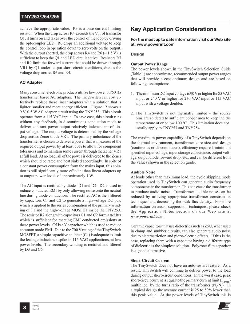
Figure 13. Recommended PC Layout for the TinySwitch.
easilyaccommodatedbyratingtheoutputdiodetohandletheshort-circuitcurrent.Theshort-circuitcurrentcanbeminimizedbychoosingthesmallest(lowestcurrentlimit)TinySwitchfortherequiredpower.
Layout
Single Point Grounding UseasinglepointgroundconnectionattheSOURCEpinfortheBYPASSpincapacitorandtheInputFilterCapacitor(seeFigure13).
Primary Loop Area Theareaoftheprimaryloopthatconnectstheinputfilterca-pacitor,transformerprimaryandTinySwitchtogether,shouldbekeptassmallaspossible.
Primary Clamp CircuitAclamporsnubbercircuitisusedtominimizepeakvoltageandringingontheDRAINpinatturn-off.ThiscanbeachievedbyusinganRCsnubberforlessthan3WoranRCDclampasshowninFigure13forhigherpower.AZeneranddiodeclampacrosstheprimaryorasingle550VZenerclampfromDRAINtoSOURCEcanalsobeused.Inallcasescareshouldbetakentominimizethecircuitpathfromthesnubber/clampcomponentstothetransformerandTinySwitch.
Thermal ConsiderationsCopperunderneath theTinySwitchactsnotonlyasa singlepointground,butalsoasaheatsink.ThehatchedareashowninFigure13 shouldbemaximized forgoodheat-sinkingofTinySwitchandoutputdiode.
Y CapacitorTheplacementoftheYcapacitorshouldbedirectlyfromtheprimarysinglepointgroundtothecommon/returnterminalonthesecondaryside.SuchplacementwillmaximizetheEMIbenefitoftheYcapacitor.
Optocoupler It is important tomaintain theminimum circuit path fromthe optocoupler transistor to theTinySwitchENABLE andSOURCEpinstominimizenoisecoupling.
Output DiodeFor best performance, the area of the loop connecting thesecondarywinding, theOutputDiodeand theOutputFilterCapacitor,shouldbeminimized.SeeFigure13foroptimizedlayout.Inaddition,sufficientcopperareashouldbeprovidedattheanodeandcathodeterminalsofthediodetoadequatelyheatsinkthediodeunderoutputshort-circuitconditions.
Input and Output Filter Capacitors Thereareconstrictionsinthetracesconnectedtotheinputandoutputfiltercapacitors.Theseconstrictionsarepresentfortworeasons.Thefirstistoforceallthehighfrequencycurrentstoflowthroughthecapacitor(ifthetracewerewidethenitcouldflowaroundthecapacitor).Secondly,theconstrictionsminimizetheheattransferredfromtheTinySwitchtotheinputfiltercapacitorandfromthesecondarydiodetotheoutputfiltercapacitor.Thecommon/return(thenegativeoutputterminalinFigure13)terminaloftheoutputfiltercapacitorshouldbeconnectedwithashort,lowresistancepathtothesecondarywinding.Inaddition,thecommon/returnoutputconnectionshouldbetakendirectlyfromthesecondarywindingpinandnotfromtheYcapacitorconnectionpoint.
TOP VIEW
PI-2176-071398
Y1-Capacitor
Opto-coupler
CBP
D
ENBP
TinySwitch
+
–
HV
+– DCOUT
Input Filter Capacitor Output Filter Capacitor
Safety Spacing
Transformer
Maximize hatched copper areas ( ) for optimum heat sinking
S
S
PRI SEC
Rev E 02/12
TNY253/254/255
10
StorageTemperature...................................... -65to150°COperatingJunctionTemperature(2)................ -40to150°CLeadTemperature(3).................................................260°CThermalImpedance(θJA)..................70°C/W
(4),55°C/W(5)
ThermalImpedance(θJC)....................................... 11°C/W
4.Solderedto0.36sq.inch(232mm2),2oz.(610gm/m2)copperclad.5.Solderedto1sq.inch(645mm2),2oz.(610gm/m2)copperclad.6.Thehigherpeakdraincurrentisallowedwhilethedrain
voltageissimultaneouslylessthan400V.
ABSOLUTE MAXIMUM RATINGS(1)
DRAINVoltage.......................................... -0.3Vto700VPeakDRAINCurrent(TNY253/4)............400(500)mA(6)
PeakDRAINCurrent(TNY255)...............530(660)mA(6)
ENABLEVoltage........................................... -0.3Vto9VENABLECurrent................................................... 100mABYPASSVoltage............................................ -0.3Vto9V
1. AllvoltagesreferencedtoSOURCE,TA=25°C.2. Normallylimitedbyinternalcircuitry.3. 1/16"fromcasefor5seconds.
40 44 48 66 68 71
-68 -50 -30
-15 -10 -5
1.10 1.45 1.80 -58 -42 -25
160 200
140 180
-2.5
5.8
0.72
CONTROL FUNCTIONS
OutputFrequency
MaximumDuty Cycle
ENABLE Pin TurnoffThreshold Current
ENABLE PinHysteresis Current
ENABLE PinVoltage
ENABLE Short-Circuit Current
DRAIN Supply Current
BYPASS PinCharge Current
BYPASS Pin VoltageBYPASS Hysteresis
kHz
%
µA
µA
V
µA
µA
µA
mA
mA
V
V
Min Typ Max
fOSC
DCMAX
IDIS
IHYS
VEN
IENSC
IS1
IS2
ICH1
ICH2
VBP
VBPH
Parameter Symbol(Unless Otherwise Specified)
See Figure 14
Conditions
TNY253
TNY255
TNY253TNY254TNY255TNY253TNY254TNY255TNY253TNY254TNY255
130
215
-4.5
-3.3
TNY254
ENABLE Open(MOSFET Switching)
See Note B, C
TJ = 25 °C115 140
265
-2.0
-5.0 -3.5
-4.0 -1.0
5.6 6.1
0.60 0.85
UnitsSOURCE = 0 V; TJ = -40 to 125 °C
TNY253
TNY255 67TNY254
TJ = -40 °C to 125 °C
TJ = 125 °C -68 -52 -45
VEN = 0 V, TJ = -40 °C to 125 °C
VEN = 0 V, TJ = 125 °C -58 -45 -38
VBP = 0 V, TJ = 25 °C
See Note D, E VBP = 4 V, TJ = 25 °C See
Note D, E
64 69
-4.8 -1.8
-6.0 -3.0
170 215
TNY253TNY254TNY255
S1 Open
See Note A
IEN = -25 µA
VEN = 0 V (MOSFET Not Switching) See Note B
See Note D

TNY253/254/255
11Rev E02/12
Conditions Parameter Symbol SOURCE = 0 V; TJ = -40 to 125 °C See Figure 14 (Unless Otherwise Specified)
di/dt = 12.5 mA/µsTJ = 25 °C
di/dt = 25 mA/µsTJ = 25 °C
di/dt = 80 mA/µsTJ = 25 °C
135 150 165
230 255 280
255 280 310
170 240
170 215
200 250
100 150
125 135 145
70
31 36 50 60
23 27
37 45
50 700
50
50
ILIMIT
Note F
IINIT
tLEB
tILD
RDS(ON)
IDSS
BVDSS
tR
tF
mA
mA
ns
ns
°C
°C
Ω
µA
V
ns
ns
Current Limit
Initial CurrentLimit
Leading EdgeBlanking Time
Current LimitDelay
Thermal ShutdownTemperature
Thermal ShutdownHysteresis
ON-StateResistance OFF-State DrainLeakage Current BreakdownVoltage
Rise Time
Fall Time
Min Typ Max Units
CIRCUIT PROTECTION
OUTPUT
VBP = 6.2 V, VEN = 0 V,
VDS = 560 V, TJ = 125 °C
TJ = 25 °CTJ = 100 °C
TJ = 25 °CTJ = 100 °C
TNY253/TNY254ID = 25 mA
Measured with Figure 10 Schematic.
TNY253
TNY254
TNY255
VBP = 6.2 V, VEN = 0 V,
IDS = 100 µA, TJ = 25 °C
TNY253TNY254TNY255TNY253TNY254TNY255
TJ = 25 °CSee Note G
TNY255ID = 33 mA
See Figure 17TJ = 25 °C
TJ = 25 °C
0.65 xILIMIT(MIN)

Rev E 02/12
TNY253/254/255
12
NOTES:A. For a threshold with a negative value, negative hysteresis is a decrease in magnitude of the corresponding threshold.
B. Total current consumption is the sum of IS1 and IDSS when ENABLE pin is shorted to ground (MOSFET not switching) and the sum of IS2 and IDSS when ENABLE pin is open (MOSFET switching).
C. Since the output MOSFET is switching, it is difficult to isolate the switching current from the supply current at the DRAIN. An alternative is to measure the BYPASS pin current at 6.2 V.
D. BYPASS pin is not intended for sourcing supply current to external circuitry.
E. See typical performance characteristics section for BYPASS pin start-up charging waveform.
F. For current limit at other di/dt values, refer to current limit vs. di/dt curve under typical performance characteristics.
G. This parameter is derived from the change in current limit measured at 5X and 10X of the di/dt shown in the ILIMIT specification.
Figure 14. TinySwitch General Test Circuit.
PI-2211-061898
0.1 μF
10 V50 V
470 Ω5 W S2
S1
470 Ω
NOTE: This test circuit is not applicable for current limit or output characteristic measurements.
D EN
BPS
S
S
S
S
Conditions Parameter Symbol SOURCE = 0 V; TJ = -40 to 125 °C See Figure 14 (Unless Otherwise Specified)
50 0.5
tEN
tDST
V
µs
µs
DRAIN Supply Voltage
Output Enable Delay
Output Disable Setup Time
Min Typ Max Units
OUTPUT (cont.)
TNY253TNY254TNY255 10
14

TNY253/254/255
13Rev E02/12
1.1
1.0
0.9-50 -25 0 25 50 75 100 125 150
BREAKDOWN vs. TEMPERATURE
PI-
2213
-040
901
Typical Performance Characteristics
Figure 17. Current Limit Envelope.
Figure 15. TinySwitch Duty Cycle Measurement.
PI-2194-062398
ENABLE
tP
tEN
tP =
1
2fOSCfor TNY253/254
DCMAX
tP =
1
fOSCfor TNY255
Figure 16. TinySwitch Output Enable Timing.
1.2
1.0
0.8
0.6
0.4
0.2
0-50 -25 0 25 50 75 100 125
FREQUENCY vs. TEMPERATUREP
I-22
38-0
3300
1
0.8
1.31.21.1
0.90.8
1.0
00 1 2 6 83
Time (μs)
DR
AIN
Cur
rent
(no
rmal
ized
)
PI-
2248
-090
198
4 5 7
0.70.60.50.40.30.20.1
ILIMIT(MAX) @ 25 °C
ILIMIT(MIN) @ 25 °C
IINIT(MIN)
tLEB (Blanking Time)
PI-2048-033001
DRAINVOLTAGE
HV
0 V
90%
10%
90%
t2
t1
D = t1t2

Rev E 02/12
TNY253/254/255
14
Typical Performance Characteristics (Continued)
1.2
1.0
0.8
0.6
0.4
0.2
0.00 12.5 25 37.5 50 62.5 75 87.5 100
di/dt in mA/s
TNY253 CURRENT LIMIT vs. di/dt
PI-
2230
-082
798
Cu
rren
t L
imit
(No
rmal
ized
to
12.
5 m
A/s
)
1.4
1.2
1.0
0.8
0.6
0.4
0.2
0.00 50 100 150 200 250
di/dt in mA/s
TNY254 CURRENT LIMIT vs. di/dt
PI-
2232
-082
798
Cu
rren
t L
imit
(No
rmal
ized
to
25
mA
/s)
1.4
1.2
1.0
0.8
0.6
0.4
0.2
0.00 160 320 480 640 800
di/dt in mA/s
TNY255 CURRENT LIMIT vs. di/dt
PI-
2234
-082
798
Cu
rren
t L
imit
(No
rmal
ized
to
80
mA
/s)
1.4
1.2
1.0
0.8
0.6
0.4
0.2
0.0-50 -25 0 25 50 75 100 125
CURRENT LIMIT vs. TEMPERATURE
PI-
2236
-033
0011.4
6
5
4
3
2
1
0
0 0.2 0.4 0.6 0.8 1.0
Time (ms)
BYPASS PIN START-UP WAVEFORM
PI-
2240
-082
898
BY
PA
SS
Pin
Vo
ltag
e (V
)
7
DRAIN Voltage (V)
Dra
in C
urre
nt (m
A)
OUTPUT CHARACTERISTIC300
250
200
100
50
150
00 2 4 6 8 10
PI-
2221
-033
001
TNY253 1.00TNY254 1.00TNY255 1.33
Scaling Factors:
TNY253/254/255
15Rev E02/12
PI-2076-040110
1
A
K
J1
4
L
G
8 5
C
N
PDIP-8 (P Package)
D S .004 (.10)
J2
-E-
-D-
B
-F-
DIM
ABCGHJ1J2 KLMNPQ
Inches
0.367-0.3870.240-0.260 0.125-0.1450.015-0.0400.120-0.1400.057-0.0680.014-0.0220.008-0.0150.100 BSC0.030 (MIN)0.300-0.3200.300-0.3900.300 BSC
mm
9.32-9.836.10-6.603.18-3.680.38-1.023.05-3.561.45-1.730.36-0.560.20-0.382.54 BSC0.76 (MIN)7.62-8.137.62-9.917.62 BSC
Notes:1. Package dimensions conform to JEDEC specification MS-001-AB for standard dual in-line (DIP) package .300 inch row spacing (PLASTIC) 8 leads (issue B, 7/85).2. Controlling dimensions are inches.3. Dimensions shown do not include mold flash or other protrusions. Mold flash or protrusions shall not exceed .006 (.15) on any side. 4. D, E and F are reference datums on the molded body.
H
M
P
Q P08A
Typical Performance Characteristics (Continued)
100
10 600
DRAIN Voltage (V)
DR
AIN
Cap
acit
ance
(pF)
COSS vs. DRAIN VOLTAGE
10
PI-
2223
-033
001
200 400
TNY253 1.00TNY254 1.00TNY255 1.33
Scaling Factors:50
30
40
10
20
00 200 400 600
DRAIN Voltage (V)
Po
wer
(mW
)
DRAIN CAPACITANCE POWER
PI-
2225
-033
001
TNY253 1.00TNY254 1.00TNY255 1.33
Scaling Factors:

Rev E 02/12
TNY253/254/255
16
PI-2077-040110
1
A
J1
4L
8 5
C
G08A
SMD-8 (G Package)D S .004 (.10)
J2
E S .010 (.25)
-E-
-D-
B
-F-
M
J3
DIM
ABCGHJ1J2J3J4 KLMPα
Inches
0.367-0.3870.240-0.260 0.125-0.1450.004-0.0120.036-0.0440.057-0.0680.048-0.0530.032-0.0370.007-0.0110.010-0.0120.100 BSC0.030 (MIN)0.372-0.388
0-8°
mm
9.32-9.836.10-6.603.18-3.680.10-0.300.91-1.121.45-1.731.22-1.350.81-0.940.18-0.280.25-0.302.54 BSC0.76 (MIN)9.45-9.86
0-8°
Notes:1. Package dimensions conform to JEDEC specification MS-001-AB (issue B, 7/85) except for lead shape and size.2. Controlling dimensions are inches. 3. Dimensions shown do not include mold flash or other protrusions. Mold flash or protrusions shall not exceed .006 (.15) on any side.4. D, E and F are reference datums on the molded body.
K
Gα
H
.004 (.10)J4
P
.010 (.25) M A S
.420
.046 .060 .060 .046
.080Pin 1
.086.186
.286
Solder Pad Dimensions
Revision Notes Date
A - 02/99
B1. Leading edge blanking time (tLEB) typical and minimum values increased to improve design flexibility.2. Minimum DRAIN supply current (IS1, IS2) eliminated as it has no design revelance.
07/01
C
1. Updated package reference.2. Corrected VR1 in Figure 12.3. Corrected storage temperature, θJA and θJC and updated nomenclature in parameter table.4. Corrected spacing and font sizes in figures.
D1. Corrected θJA for P/G package.2. Updated DIP-8 and SMD-8 Package Drawings. 3. Figure 10 caption and text description modified.
04/03
E 1. Changed SOA limit. 02/12

TNY253/254/255
17Rev E02/12
Notes

Rev E 02/12
TNY253/254/255
18
For the latest updates, visit our website: www.powerint.comPower Integrations reserves the right to make changes to its products at any time to improve reliability or manufacturability. Power Integrations does not assume any liability arising from the use of any device or circuit described herein. POWER INTEGRATIONS MAKES NO WARRANTY HEREIN AND SPECIFICALLY DISCLAIMS ALL WARRANTIES INCLUDING, WITHOUT LIMITATION, THE IMPLIED WARRANTIES OF MERCHANTABILITY, FITNESS FOR A PARTICULAR PURPOSE, AND NON-INFRINGEMENT OF THIRD PARTY RIGHTS.
Patent InformationThe products and applications illustrated herein (including transformer construction and circuits external to the products) may be covered by one or more U.S. and foreign patents, or potentially by pending U.S. and foreign patent applications assigned to Power Integrations. A complete list of Power Integrations patents may be found at www.powerint.com. Power Integrations grants its customers a license under certain patent rights as set forth at http://www.powerint.com/ip.htm.
Life Support PolicyPOWER INTEGRATIONS PRODUCTS ARE NOT AUTHORIZED FOR USE AS CRITICAL COMPONENTS IN LIFE SUPPORT DEVICES OR SYSTEMS WITHOUT THE EXPRESS WRITTEN APPROVAL OF THE PRESIDENT OF POWER INTEGRATIONS. As used herein:
1. A Life support device or system is one which, (i) is intended for surgical implant into the body, or (ii) supports or sustains life, and (iii) whose failure to perform, when properly used in accordance with instructions for use, can be reasonably expected to result in significant injury or death to the user.
2. A critical component is any component of a life support device or system whose failure to perform can be reasonably expected to cause the failure of the life support device or system, or to affect its safety or effectiveness.
The PI logo, TOPSwitch, TinySwitch, LinkSwitch, DPA-Switch, PeakSwitch, CAPZero, SENZero, LinkZero, HiperPFS, HiperTFS, HiperLCS, Qspeed, EcoSmart, Clampless, E-Shield, Filterfuse, StakFET, PI Expert and PI FACTS are trademarks of Power Integrations, Inc. Other trademarks are property of their respective companies. ©2012, Power Integrations, Inc.
Power Integrations Worldwide Sales Support Locations
World Headquarters5245 Hellyer AvenueSan Jose, CA 95138, USA.Main: +1-408-414-9200Customer Service:Phone: +1-408-414-9665Fax: +1-408-414-9765e-mail: [email protected]
China (Shanghai)Rm 1601/1610, Tower 1,Kerry Everbright CityNo. 218 Tianmu Road West,Shanghai, P.R.C. 200070Phone: +86-21-6354-6323Fax: +86-21-6354-6325e-mail: [email protected]
China (ShenZhen)3rd Floor, Block A,Zhongtou International Business Center, No. 1061, Xiang Mei Rd,FuTian District, ShenZhen,China, 518040Phone: +86-755-8379-3243Fax: +86-755-8379-5828e-mail: [email protected]
GermanyRueckertstrasse 3D-80336, MunichGermanyPhone: +49-89-5527-3910Fax: +49-89-5527-3920e-mail: [email protected]
India#1, 14th Main RoadVasanthanagarBangalore-560052 IndiaPhone: +91-80-4113-8020Fax: +91-80-4113-8023e-mail: [email protected]
ItalyVia De Amicis 220091 Bresso MIItalyPhone: +39-028-928-6000Fax: +39-028-928-6009e-mail: [email protected]
JapanKosei Dai-3 Bldg. 2-12-11, Shin-Yokomana, Kohoku-ku Yokohama-shi Kanagwan 222-0033 JapanPhone: +81-45-471-1021Fax: +81-45-471-3717e-mail: [email protected]
KoreaRM 602, 6FLKorea City Air Terminal B/D, 159-6Samsung-Dong, Kangnam-Gu,Seoul, 135-728, KoreaPhone: +82-2-2016-6610Fax: +82-2-2016-6630e-mail: [email protected]
Singapore51 Newton Road#15-08/10 Goldhill PlazaSingapore, 308900Phone: +65-6358-2160Fax: +65-6358-2015e-mail: [email protected]
Taiwan5F, No. 318, Nei Hu Rd., Sec. 1Nei Hu Dist.Taipei, Taiwan 114, R.O.C.Phone: +886-2-2659-4570Fax: +886-2-2659-4550e-mail: [email protected]
Europe HQ1st Floor, St. James’s HouseEast Street, FarnhamSurrey GU9 7TJUnited KingdomPhone: +44 (0) 1252-730-141Fax: +44 (0) 1252-727-689e-mail: [email protected]
Applications HotlineWorld Wide +1-408-414-9660
Applications FaxWorld Wide +1-408-414-9760


