
INDUCTION rv:O·rOR DRIVE FOR BATTERY VEHH1LE.
BY
!Vi. I,IALENGRET.
Thesis submitted to the
Department of Electrical Engineering
. of the
University of Cape Tovm
for the degree of
M. S c • ( Eng. )
I978 1'-,

The copyright of this thesis vests in the author. No quotation from it or information derived from it is to be published without full acknowledgement of the source. The thesis is to be used for private study or non-commercial research purposes only.
Published by the University of Cape Town (UCT) in terms of the non-exclusive license granted to UCT by the author.

CONTENTS
I. Acknowledgement.
2. Abstract.
3 Chapter I
Introduction
Pg I
Pg 2
4 1.1 The Importance of overall cost. Pg 3
5 1.2 The Importance of overall efficiency Pg 4
6 1.3 The Importance of Regenerative Braking Pg 6
7 Chapter II.
8
9
10
Variable Speed Motor and its application
to Battery Vehicles.
2.1 The Induction Motor as opposed to
D.C.Motors
2.2 Reasons for a 9 Phase Induction ff.otor ,
2.3 The Induction Motor Analysis
2.4 Direct to Wheel Drive
II Chapter III
12
13
14
15
The 9 Phase Interlaced Inverter
Introduction
3.1 The Single Phase Full Bridge Inverter
3.1.1 The Basic Switching Action
3.1.2 The Voltage Control
3.2 The Principle Of Interlacing
3.3 Time Delays Prevent Problems
16 Chanter IV .
The Transistor As A Switching Device
In The Proposed Inverter
4.1 The Power Trancistot' us a Switch
~Fg 8
Pg 9
Pg 10
Pg 14
Pg 16
Pg 16
Pg 16
Pg 21
Pg 2 3
Pg 23
Pg 29
17 4.2 The Transistor or The Thyristor
18 4.3 Paralleling Transistors
19 4.4 Transistor Breakdown Mechanism
20 4.5 The Darlington Configuration
21 4.6 Requirement of the Transisror Bridge
Diodes
22 4.7 The Loss Mechanism in Transistors
23 Chanter V
The Logic which Implements the Switching
Function of The 9 Phase Interlace Inverter
5.1 The Logic Controller
24 5.I.1 Summary of Logic
25 5.I.2 The Oscillator
26 5.1.3 The M/S Generator
27 5.I.4 The Divider
28 5.I.5 The 8/IO Generator
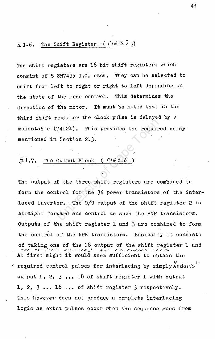
29 5.I.6 The Shift Register
30 5.I.7 The Output Block
31 Chapter VI
32
33
34
35
36
37
Design of the 9 Phase Motor
6.1 Torque Requirement
6.2.Design of the Stator Core
6.3 Winding Design
6.4 Maximum Speed At Full Phase
Chapter VII
Construction of the Motor Invertor Assembly
7.1 Stator
7.2 Winding
7.3 Inverter
Pg .32
Pg 33
Pg "J5
Pg .37
Pg 38
Pg 40
Pg 42
Pg 42
Pg 42
Pg 42
Pg 45
Pg 45
Pg 43
Pg 43
Pg 52
Pg 52
Pg 53
Pg 56
P~ 59
Pg 59
Pg 63

38 Chapter VIII
Results of the 9 Phase Inverter Fed
Induction Iljotor.
8.1 Stalling Torque
39 8.2 Magnetizing Curves
40 8.3 Load Test at Full Flux
41 8.4 Load Tests for variable Frequency
42 8.5 Load tests when Chopping
43 d.6 3 Phase Sinusoidal Test
44 8.7 Oscillograms
45 8.8 Proposed Modification to Motor
46 Conclusion
47 Appendix,q
48 Appendix B
49 Appendix C.
50 Appendix 0
5I Appendix E
52 Appendix F
53 Appendix G
54 Appendix H
55 References
Pg 69
Pg 70.
Pg 70
Pg~72
Pg 76
Pg 79
Fg31
Pg 81
:fig 86
Pg 87
Pg 83
Pg 90
Pg 93
Pg 96
Pg 98
Pg 121
Pg I24
Pg 128

ACl:r~OWLE:}EMENT
To my supervisor, Froffesor N.C. de V Enslin, I would
like to convey my sincere appreciation for his guidance
and encouragement.
Thanks are due to the C.S.I.R. whose generous financial
support has made this project possible.
Thanks are also extended to Mr.M.Attfield and lfr.'N.Wright
for their technical help.

ABSTRACT .
A 9 phase transistor inverter fed induction 'motor for a
battery vehicle with direct wheel drive is discussed. A
new method of motor voltage control by pulse, width
modulation, where the,phases are ~nterlaced in a manner
to conserve continuity of the supply current, is
described. In addition to this, a novel construction,
where the motor and the inverter are built into one
compact and economical unit, is presented.
I

2
CHAPTER I .
INTRODUCTION
Despite the numerous advantages of the electrical vehicle,
it ha.s not reached any significant pcrcentnge . of modern
day transportation. The lack cf suitable means of
storing electrical energy has been claimed to be the
major drawback. Nevertheless, even with today's
technology it's wider application could have enormous
repercussions towards solving some pertinent questions,
such as the energy crisis and environmental pollution
caused by the combustion engine.
The momentum of battery research and development is
gaining unprecedented proportions and evidence of an
imminent major breakthrough is becoming too significant
to overlook. I ,2,}
Due to the time lag involved between development of a
prototype and mass production it is of utmost importance
that areas other than energy ztorage should be thoroughly
investigated now.4 One area which requires particular
attention is the propulsion system. Measurements indicate
that vehicle range can double through propulsion systems
improve~en~ alone. 5

This project is particularly concerned in producing a
flexible, efficient and cheap drive. The drive is a
9 phase transistor fed squirrGJ cage induction motor
with sufficient torque and flexibility for a direct
drive without a gear box or differential. The motor
voltage control is achieved by the popular method of
pulse width modulation, but with the novel approach of
interlacing between the phases. The advantages of
interlacing are numerous and solve problems associated
3
with the application of power transistors to' inverter fed
induction motors. The production of high voltage peaks
and switching losses are drastically reduced by inter
lacing, thus enabling the use of cheaper transistors and
increas~ in overall efficiency.
1.1 The Importance of Overall Cost
An analysis done by the G.E.S. Group in West Germany,
which compares electrical vehicles to petrol driven
counterparts, has found that series production cost of
electric cars is about Ii to It times that of it's petrol
driven equivalent; with operation costs about the same,
probably with a slight advantage for the electrical
vehicle if a long life version is developed. The above
economics mi~lt be acceptable to a fleet owner, but
surely would not be so tempting for the. private motorist.

It is therefore important that more effort should be made
to cut down expenses on certain critical areas.
4
The traction motor accounts' for a bie s~1ar~ of' the cost of
electricaT ve~tcle3~ Th~ D.C. ~otor used normally is far rnor0
expensive" than the' internal conbustion engine, probably bec~usc 6
of it IS limited production. The transmis'sion 1'5 C!nother costly
lter.1 as' it normall'y contains many moveable part1.~Tbe possibility
of'eliminating it should strongly be considered for this renson
alone.
If the electrical vehicle could improve it's cost by say
25% a major 'shift away from internal combustion engine
would be imminent. "In any case as petroleum products
increase, the cross over point will soon be reached.
1.2 The Importance of Overall Efficiency
The conversion efficiency considered is effectively a
system efficiency (i.e. the fraction of power supplied
by the battery which is actually available at the wheels).
This overall efficiency is comprised of the individual
efficiency of several vehicle components, but predominant
ly by the controller, motor and transmission. While each
of these three components may be designed to be hiehly

5
efficient, the resulting efficiency is the product of the
efficiencies of all three and is not nearly so impressive.
Under present day developments it appears that the best 5
overall efficiency is in the region of 70%. Although
the battery efficiency is not included in the above
defined conversion efficiency, it must be stated that the
method of power extraction of the system wiil have
profound influence on the battery efficiency. Any system
which takes power from the battery under steady conditions
as opposed to under pulsed conditions, will increase the
b tt ff ·· 11 Th b tt . t nal . t aery e 1c1ency. e aery 1n er reS1S ance
and supply leads will experience IQsses in accord with the
·fU~S current 5Qu~-re a'q opposed. to' the output brrsed' on 'the average
current-". T11.e ca1Yaci tive property of the' "battery ':1il~1 offset
--the- effect to' some extent.
The proposed drive in this project could be optimised
and overall efficiency as high as 90~ should theoretically
be possible. The efficiency of a transistor inverter could 8 reach over 97%, especially in the light of reduced effect
'of stored magnetic energy of the inverter and supply on
switching losses. The efficiency of the squirrel cage
induction motor coul d be as high as 9~~~ with special 9
attention paid to low rotor resistance. The trans-
missions having been eliminated would leave bearings and
universal joints only. Maximum mechanical efficiency is
6
secured if the traction motor or motors are fixed at the
wheels and rotate at wheel speed. But as the heavy motor
will need to be sprung, the need of a flexiple connection
such as a universal joint is required. The next option
would be to use a high efficient chaln drive with little
or no gear ratio.
··The· effect of incl'eased efficiency on range is· more t11an
simply linearly , related to- effic iency- as it 1 S improve--
ment implies less· ba.ttery 'Height com-poundei 1.;i th lighter·
vehicles •. For lead acid battery a forrmJac is given for' ,
range:: : :Range is· 'Prcportional to efficiency· to the pO':Tcr
of'1".325 .. Thus· an increa·se from 70% to 90~ in overall I.325
efficiency resul ts- in a range of (90/70) times as
much • That is 40% increase in range.
1.3 The Importance of Regenerative Braking,
The basic concept of regenerating is to change the motor
into a generator that pumps kinetic energy back into the
battery when braking. The major benefit of regenerative
braking is, of courGe, the extended range provided by
battery recharge. Theoretical estimates of the 8J'IlOunt
of recoverable energy range from 10 to 40%, but the
maximum obtained in service seems to be about 12%. 10
F'igures like 3 or 4% are more cammon. A secondary

7
benefit of regenerativebralti,ng is the saving on brake
wear, a substantial problem with a heavy vehicle such
as a battery car. Another advantage is that regenerative
brm~ing keeps the electrolyte from forrr:ing layers of 10
different acidity within the battery. ;~s a result more
of the acid is effectively used in both charging and
discharging and battery life and efficiency are increased.
Finally, an important psycholog~cal effect is to give the
car a driving feel like that of an internal combustion
engine vehicle, by regenerating slightly as soon as the 9
acceleration pedal is released. Unfortunately,
regenerative b'raking requires a certain amount of
complexity of the controller to limit the current and
obtain the desired deceleration. The complexity might
be a stumbling block in the development of the controller
for a prototype vehicle with an induction motor. But in
a series production a single integrated circuit (I.C)
could be sufficient to provide this fUl1ctt'on in an'
'induction motor 'which does' not require additional power
seffiiconauctors or contactors to regenerate.
..

CHAPTER II
VARIABLE SPEED INDUCTION MOTOR AND IT'S APPLICATION TO
BATTERY VEHICLES
~l The Induction Motor as opposed to D.C. Motors
Both the D.C. motor and the squirrel cage induction motor
have been proclaimed as suitable for battery vehicles,
but because the induction motor requires a variable
voltage and variable frequency supply, the cost and
complexity of the controller has discouraged a wider 1
application. Nevertheless with the decreasing cost and
increasing power handling capability of semiconductors,
the inverter driven-induction motor has become cheaper
and more powerful. The ability of integrated circuits
8
(I.C. Y to replace complex netvTOrks has made the controller
cheaper and more reliable.
The induction motor is more robust, cheaper, (see Fig.2.')
maintenance free and has a higher power to weight ratio 1,8
(kw/kg) than the D.C. motor - these points should justify
the use of the inverter fed squirrel cage induction motor
rather than the D.C. system for propulsion of on-the-road
vehicles.

9
FIGURE 1.1.
totally enclosed
explosion proof'
10 I9
Cost of' various' l-:incls of motors azainst pm-Ter ratings. -
2,2 Reasons for a 9 Phase Induction Motor
An induction motor with a large number of phases is the
most appropriate kind of motor to provide high torque and 12
smoothness of operation. However the cost, weight and
size of the inverter must not be increased substantially.
Increasing the number of phases can readily be achieved
. with a conventional machine winding, having sufficient
number of slots, by regrouping the stater coils to provide
th b f 1 t - I3 Th d' , -e necessary num er 0 supp y connec 10ns. e 1V1S1on
of the total inverter rating into a greater nUmber of
phases reduces the required current rating of individual
semiconductors, so that greater output ratings could be
achieved with existing device without parallel operation.
The inverter was constructed on the end plate carrying the
bearings of the rotor (see constructionChapter Vthercfora
individual leads are short, off ~sGttinr, the cost of the
increased number of leads required.

10
13 MacLean after investigating the performance of 3 phase
and higher number of phase induction motors concludes
that inverter circuits producing 3 phase square-wave
.. vol tages will produce a low 9ff.i ciency drive',\vhilc a 9
phase example gave almost identical performance figures to
a similar sinusoidal fed 3 phase machine.
2.3 The Induction Motor Analysis
A per .... phase equivalent circuit commonly used to analyse
. d t· t 9. h . 1;. 2 2 an 1n uc lon mo or lS s O\vn ln flgure ~.
FIGURE 1.2
Rauivnlcnt circuit of an induction tlOtOl".

II
The synchronous speed of rotating field, Ns = l20f/p
is directly proportional to f, the applied frequency.
The frequency of current, in the rotor is (s5) the slip
frequency. (This can be negative when regenerating). 9
The torque developed can be expressed as
~ = flux per pole
where e
Cos e 2 is the rotor power factor
=
L2 and R2 are the rotor leakage inductaYlce and resista.nce
Em =
If the back emf E~is kept constant for different frequencies
the flux is inversely proportional to the frequency. The
torque speed curve obtained in this way is sketched in
Figure 2.3

..-, , . \'llOCU5 of constant pO\.,er
, .", t:\-H., for a cons tan t Q-lil
~ "'~'" II _ ... ~\ .. . \ '. q ~ \ ' locus of constant torque ~ -+\-¥#-:'#.~'" for constant En/f-
.~' , I •• ~ \ \ .... 1.. 'I '
_,. I ""- ' .., , · ~ '....... l- _ .. -', I , ;:: • ....::'_ ' ~ __ --l----' T _ _ --:- ... -.~.= .. :: . .:.:... .. ----,- ,- _ .. - --\ , ..... --L .- - , - , \ \ .-- , , '. ,
12 Torque speed characteristic for constant Em andRm/f
At higher speeds' \-There R2is ~2ffl~ and \·mere the
motor is running at small slip (which is normally
the case) then the average IDechanical power output of .12 -
the motor is
~ =- back e .. m.f.
when m is the number of phases. It is seen that if the
slip and E is kept constant the motor will run essentially m
at constant horse power. Although it is desirable that
the average mechanical power output of the motor be
approximately constant over a wide range for a given 12
accelerator displacement, such a characteristic cannot be
maintained at very low speeds because of .conseql1ent rapidlv
increasing current. By making Em proportional to the
speed of the motor at low speeds the current would
remain within it's limit and the torque would be constant
for a given accelerator' displacement. The maximt.l..:1 pullout
torque ,·mula be obtained vThen the apnlieu frequFiTIcy ~·'ill render
the rotor J.(-!a~l:age reactance eaual to R2lso

I3
A locus of steady state operating points obtained in this
way is shown in Figure 2.3 for a particular acceleration
pedal displacement.
As Em is not an accessible variable, the applied voltage
is controlled. If the applied voltage, instead of Em is
made directly proportional to frequency at low frequencies,
the torque is not constant because of the volt drop inthe
·re5istanco ()~ the stator" " 'l:linri in itS" v1hich starts- to' cTomin::lte
th t t I k t · . t d I4C t· e s a or ea age reac ance 1n magn1 u e. ompensa 10n
can effectively be made with a voltage to frequency linear
relationship which is offset from the origin as shown in IS
Figure 2.+-
Voltage
. .. ,
. ,/ constant Etunly volt::,~e :./ JC'" bocnuse of :r:ra;:inu:,l a-\tailablc
voltae'G ~ required yol tarre for"
constant torque operation.
,
Frequcncy llequired vol t::iRe for ·cnnstant torcrnc.
As an induction motor operates as a slipping clutch the
slip frequency must be ,kept as small as possible by a high
flux (hiBh Emlf). Nevertheless, the motor must be kept
from over-saturation which results in increase magne"tizing
current and losses.

I4
2..'t Direct to Wheel Drive
The induction motor contemplated is to produce Dufficient
torque at low speeds so that no gear reduction is required.
A, direct drive would therefore imply a relatively low
speed motor. Because the squirrel cage inductio~1 motor is
robust and has no commutator it can run at very high speeds.
Hence a higher power to weight ratio can be obtained
(kw/kg) than a D.C. motor. However, with a low speed
induction motor this advantage would be lost in favour of
the benefits of no transmission at all. It is, therefore,
debatable whether the weight of the transmission and
mechanical inefficiency is more unfavourable than a heavy
and more expensive low speed motor. In the case of a D~C.
motor the ar~~ent brought forward by pro-transmission 16
people is that the motor draws heavy current to produce
high torques at low speeds, and therefore reduces the
range. The described interlaced induction 'motor with
it's ability to produce high torques with drastic reduction
in supply current compared to conventional motors destroys
this convincing argument. (see chanter ~ ). The heat
losses dissipation within the motor will however be
favoured less than with low speed motors. Forced cooling
will be required, especially when driving up steep grades
for extended periods. In any case, this is normally
needed in transmission type electrical vehicles.

15
The l"'..echanicaI trns~ission lossoS' account for as much ClS
10% of the power produced in conventional drivcs(see appendix A),
and substancially reduces the benefit of regenerative braking.
The- range' reduction \'lOuld therefore be over IO~, especially
in tm-m driving. This crluld be translatcd in at least IO~
increase in battery weight, and electrical cost.
A further point is the differential action required
between the traction wheels. A separate induction motor
on each traction wheel, which all run at the same air gap
frequency has this inherent characteristic. The traction
force is only applied to the wheel which has grip to the
road surface as the torque drops very qu.ickl¥, wi th little
increase in speed. A single stator construction with two
rotors which can freely rotate could be another solution which
would reduce the overall ratio of overhang copper to active copper.
It must be noted that' when cornering the faster wheel
. must not go into negative slip as the bral:inK action
would affect steering.
Reversing with an induction motor is simple and does not
require a heavy contactor or gear, as in the case of the
D.C. motor. Reversal is obtained by reversing the phase
sequenc9 to the inverter.,. '"rhich is obtnineri at the Im·r
est pOHer level •.

CHAPTER lIT
THE 9 PHASE INTERLACED INVER,..ER
INTRODUCTION
In this Chapter the method- of'power conversion, from D.C. to
A.C. power for the proposed motor is p.r e seli1:"ed ~ The
9 phase inverter consists of 9 conventional single phase
full bridge inverters. The single phase bridge is first
dealt with, to describe the basic switching action. The
principle of interlacing between the 9 phases is then
discussed and finally the logic control for the transistor
awi tches.
device.
The transistor was chosen as the switching
17 3.1 The Single Phase Full Bridge Inverter
3~I,1. The Basic Switching Action
To convert the D.C. voltage supply to an A.C. voltage, a
modulation or switching device must be contemplated. A
modulation of the voltage can be obtained by switching a
phase progressiv~ly, however tho difference of the supply
and phase voltar.e r(l~uJtS' in exct?s~ivl3 pOHer los~err in th~
device. Althour,h a sinusoidpl "(oltaee 'tr~veforn is ide::Jl
for an efficient operation of an induction motor,

I7
the production of sinusoidal voltage waveform by modulation
of the supply would be intolerably inefficient and I
impractical. An A.C. voltage waveform of a square or
quasi-square waveform nature is therefore produced by
"fast" switching. The ideal switching action would be
an instantaneous one which would result in no loss.
The basic switching action for a square voltage waveform
is illustrated in Figure3Ia and3Ib :
. FIGtE18 1. I • . (a)
SI lSI
b a
Vb
s4
Sin~lc ~hrrso bridre invertor switching sequence to produce a squnrc vol ta;',e lTaveforn.
The switches Sl and S4 are controlled to connect a to the
positive line and b to the negative line for half the
positive cycle. The negative cycle being produced in a
similar manner by S3 and S2 the resulting waveform is
shown in Figure 2.

FIGURE .,. 2' ~).
, Vb 0' d
0 I80 360
-------- ---.
...... rJ Single phase sqare voltage waveform
An induction motor always runs with a lagging power
factoro An alternate path for the current, which must
still flow when the voltage is removed must be provided.
Hence the need of diode Dl,D2,D3, and D4, see
Figure 3.3 The freewheeling diodes are arranged to enable I
reactive load energy to be circulated and regeneration
into the D.C. links to take place.
FIGURE 3 .3
a b
Vb
s4
Single phase full brid[',e inverter Hith i'reeHeeling diode
1'3

For example at the e~d of the positive cycle Sl and S2
are switched off, current which has been flowing through
the load from a to b will continue to flow through D2
via the supply and back through D3, Although S3 and S2
~ill then be 'ready to conduct they will remain idle until
current in the a to b direction has ceased. Only then
'will the negative current cycle start. It must be noted
'that there is a time during each half cycle when the
inductive load feeds back power to the D.C. supply source.
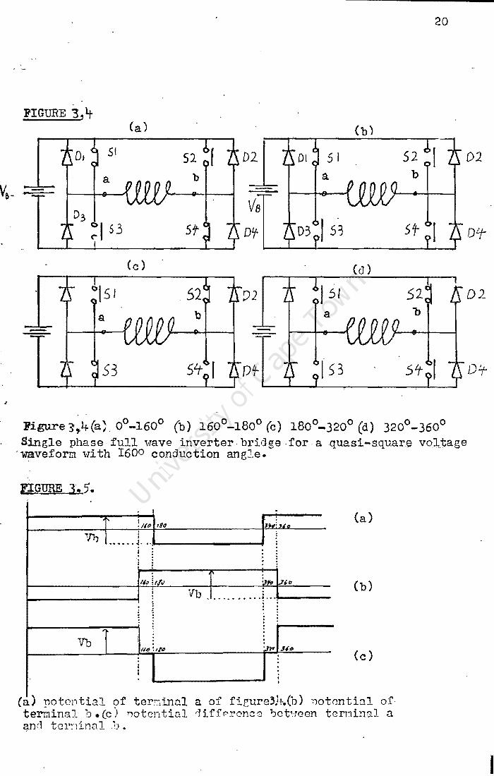
A quasi-square waveform is obtained in a similar way, but
one of the conducting switches of the above is turned on
for a shorter interval. S2 and S3 were chosen to be
, switched for a shorter interval. Sl and S2 could have
~ust as well been chosen. The switching sequence for a
conduction angle of 1600 is given in Figure3.4. The
conduction angle being the time during which both switches
of a particular half cycle are on. "
The resulting voltage uaveforn is shmm in figure 3..5
With an inductive load, current will again lag the voltage
but the lagging current will not necessarily need to flow
via the supply as with the square wave inverter (e.g.
when S4 is switched off, current will flow through D3, the
positive rail and back through Sl, only when Sl is also
disconnected will the current return via the supply
I9
V&_
,
20
FIGURE 3,4 (a)
51 51 Di 51 a
52 b
01
a "
D3 ~I S3 I
(c)
a -
S3
b
VB Sf DLf
,52 b
D'I-
I 5~
a
153
51 b
5't
Pigure 3',4 (a) ,0°-160° (b) 160°_180° (c) 180°_320° Cd) 320°-360° Single phase full i,rave inverter. bridge . for a quasi-square vol.tage '~veform with 1600 conduction ane1e.
• I
(a)
"J'li i ...... ~ ..... '---------f j : : : :. :.. t :
: : : :
Vb ; ........... ~ ... ,... ---. . : : ; E ! :
I-----~-~
· . · . · .1-----
(c)
(a) Dotcntial of ter!:',innl a of fieure3)+.(b) ~')otGnti3l of terminal b. (c) T)otcntin.l (liffE'rence botHeen tcrT1in~J. a gnd tcrninnl .b.
Dtt
01
D1t
I

2I
3.1.2. The Voltap;e Control
l-Iost inverters require a' means of' voltage"' control becau~rc of'
va-ri'a'tion in the inverter sour6e vol ta~ e, regulation ,n:thin the
inverter and most of all because a variable speed induction
motor requires- a' variable frequency as",.,ell as a variable
voltage. T.nis· is necessary to' obtain control of the air gap
flux-so as to oTlerate the' induction motor in an efficient and
flexible manner'.
The quasi-square voltage waveform described, has a fixed
fundamental vqltage amplitude for a particular conduction
angle. The harmonic content of the inverter phase voltage
is given in Appendix H It can be seen that the funda
mental voltage amplituoe can be reduced by'narrowing the ,
conduction angle. But this is not a practical voltage
control as the amplitude of the harmonic voltages can
approach the magnitude of the fundamental voltage. There
fore this mode of voltage control must be discarded.
A very popular method of controlling the voltage in inverter is
pulse width modulation, where many pulses occur during
each half cycle of the fundamental frequency. This is
obtained by switching on and off S3 or S4 during the
positive or negative ?ycle respectively.

When S3 or S4 are switched off current will cease from or
to the supply (depending whether motoring or regenerating)
and the existing current in the load will circulate by
means of diode DI or D2 (see Figurel3). This current will
decay or rise depending on the time constant of the phase,
the combined volt drop across the transistor and diode
concerned, and the voltage which may be induced within
the motor phase itself. When S3 and S4 are again switched
on current will again flow from or to the supply and will
22
rise or decay depending on the supply inductance, resistance,
the supply voltage, the transistor voltage' drop conce~nej, the
phase time constant, an9 the induced voltage. The inter
mediate time is the commutation time. It will depend on
the speed of the semiconductors as well as the inductance
and capacitance within the semiconductors and the
connecting limb concerned. The voltage waveform obtained
by the above pulse width voltage control is shown in
,Figure. 3. 6
FIGURE 3.6
,- r 1-
L I C
Chopper modulated voltarc waveform

r'
The ratio of the on time to the off time is known as the
mark-to-space ratio. The effective voltage is controlled
by varying the mark-to-space ratio, as the motor phase
integrates the applied voltage over a half cycle.
3.2 The Principle of Interlacing
The principle behind interlacing between the phases is to
keep the supply current from the D.C. source as continuous
as possible. The rule which applies is that a transistor
is always switched on when another is switched off.
Supply current will transfer from say coil I to coil 2,
without supply disruption, if and only if the current is
equal in magnitude and in the same direction.
23
Aquasi-square \vaveform with 1600 conduction angle. , enables
one,when"'etepping", the provision of 9 phases and 400
displacement, so that a phase is always switched on when
another is switched off (see Figure3.8). However, when
"stepping", that is at the beginning of the half period of
a phase, current which is still flowing in the opposite
direction to the appli~d voltage (since lagging power
factor) cannot assume an immediate reverse direction or
magnitude. Hence the off going phase will have to
regenerate the whole or part of it's current to the supply.
Therefore there will be a certain amount of discontinuity

A
-F
B
-0
c
-H
o
-J
E
.. ~ ~m--L
~ ~ -----.~ (
~ ( ~....--------,~ ~
~ . ~ ~
-( ~ ~ ~( ~ ~ -~ ~ .. ~
Figure 3.8 Voltage ,·ravef"orm of the 9 phase "lith T60oconduction angle at full HIS ..
f\)
~

in the supply current at the beginning of each phase
voltage period. It will fortunately only consist of one
eighth of the total supply current (see FigurelS).' In
the case of chopper modqlation it is different. Virtually
com'plete continuity of,' the supply is achieved, apart from
the abovementioned current disruption, which exists at the
beginning of each phase voltage waveform. Pulse width , '
modulation is normally applied' by' wIsing on and' off',' all
the phases simultaneously. This would defeat the idea of
switching on a phase when another is disconnected. Hence
the phases are not simultaneously chopper modulated. But
the chopper modulation is phase displaced, so that a phase
is always connected to the supply when another is
disconnected. The supply current will be virtually
25
continuous between pulses, p'rovided the 'chopping' frequency
is high enough, not to permit the current to decay
appreciably during the off period. When a phase is
disconnected, the current simply comutates to another as
long as the existing current in the latter is virtually
the same as the first. Interlacing as described, can be
obtained for 8 discrete mark-to-space combinations. Figure 3. 9
demonstrates the above principle for a four-eighth
mark-to-space ratio. Notice how for any particular time
a switching off operation always corresponds to a switching
on somewhere else. For' e.g. nt tiMe t, phase F i3 s'Hitchc,-j'
on ,[hile phn r-;o H :1~' sui tched off.1 the S0r1e :! t tir~o tJ., for
phnne E ~nd' G.

i; " I, I, ., !
fT·• I • " ., I ., •• 1,1,. I 'I
I " i" ,. ,'i" I'" 'I, t. \ •• ;"1" ;, : ! ! ' : ~ I : : -.,-;-T'~ to, I'·.·' : . : : I : : ! ~ , I ' , .. I .• • , •• i ,.-
·'· .. ·/·1 ""1' ..... ' ... ..... • to'
, .j il : !11 ! I !i " :: : , "'1' I • • , •• , I, .",.1, .• 1
j 11 ,.[ i· l : :! i:i l: t; i 1; I j I ij; 1;,; 1':1'11,:.;:;; ':.'Il/TI':
I , • ~ •• • I ,. ••• , ., •• • • ••
~.j~., .. -.. :-:-:-. -.' -:;'-,. ~I :-:- I':' t • , •••
,'j _" t I;. II: 1 ._1; ••• , •• ,. It ",t-, .... :!.:.:~: r:tt:::.! ::~~:!!:~ ';:~.;:~·:I :!t:~,::: I" .... 1" ,-, I .. ~ , •... ~. I It. I • • •• • ~ t • , , ! • I
t" ••••••••
,~- r'''-mllT , •• 0.· t • I ;!!:,::\: . I! J \ I • , •• I • • • ~ ,I. I It. '" t ••• It " It t
! I':: :: : I 11]111 111 · I., .... 01.,/ 1'1 "" f' t I t._ 'I i-I" _.-.-1- .. ___ .. __ .. , I' ..... , .. ," ",III · i ; ! ~ ! : : i : I ; : It' "I" t l " • t .•• It t t : : • : f : ~ l: .,. 1 I •
26

", .
27
The quasi-square waveform provides a meansof circulatir.g
part or all of the laeeing current, depending on the power
factor of the load. It is obvious that less losses will
.result if this current is to be allowed to circulate
. within the inverter rather than the supply, especially
with a battery where the charge discharge cycle is at the
.best 80% efficient.
Figure 3.7 illustrates how the current lags the voltage. Two' . .
distinct lagging periods are observable. One where the
current circulates within the inverter(t,) and one "There it
regenerates to the supply (t2.,) • 1:1e oscill_o'"'r::Y1 ')~1otO"'.J:,:-:"')11S
were 'obtained with t~2 motor ]escrihed in eDpendi~6~
FIGURE 3.7
----'~=-----
--.--f·f-(/(((fl/(II/I!I-(ff(//(/f(((II//!f/!I(/(((fr
I(~· "",ps
, .
OscilloCr:li:1 photo(lrn"Ph of a )phasp. current tn the 9 ph:1~~ inv('rt,~l'
b)tiha~c voltnce c)sunply cnrrnnt frOM battery.

23
3.3 Time Delays Prevent Problems
Unless special preventitive techniques are used in the
bridge inverter, it is possible that all legs of the bridge
will conduct simultaneously during the finite switching
duration. When this occurs, a potentially destructive
current is drawn which is limited only by the transistor
beta. This condition can be prevented if a time delay is
introduced at the first positive going edge of the signal
controlling S3 and S4 switches.
The voltage waveform for a particular phase full bridge
inverter is shown in Figure 3.3 The output of the inverter
is a quasi-square waveform with n x 8 cnopping pulses per
cycle. Notice how the beginning of pulse S3 and S4 are
delayed by a finite amount. The logic will therefore
require to incorporate this delay for smooth operation of
the inverter.
FIGURE 3.8
~D
Quasi square voltage waveform with 4/3 Mis ratio and front edge delay

29
CHAPTE] IV
THE TRAHSISTO!1 AS A SNITClIIHG DSVICE IN THE P!10POSEJ nrm:1TF.;{
Some verY'important areas of application and cuircuit a.daptntion
of the transistor are discussed in the folIO'\·Tin~ subsections'.
Reasons are given for the choice made in the des'ign of the
inverter'-
4.I The Pm-reI' Transistor As A S,rl.tch h
High pm,rer transistor 'tvere used to perform the svli tching function
of ,Section 3. 1 and 3.2. Figure 4.I shm·rs the transistor ~arlington
c'Onfiguration to provide suitches"SI.S2,S3 and 54 mentioned in
the .single phase full bridge inverter of Section 3.I and 3.2
Fi'gure 't.2 shows hm-r all the transistors ar'e arranr~p.d to provide
the 9 phase inverter ,·1hich essentially consi ts: of- 9'. sinp.:lFl phase
full bridge inverter. The frem-rhceling ant] regenerative
are also sh01m. The diodes' are Motorola diodes M.R. 702
~e positive rail transistors are PNP (Sl, S2) types and
the negative rail NPN (S3, S4). The power transistors
diodes
•
used are the Motorola MJ802 and MJ4502. The driver
transistors are the 2N3055 and 2N5530 - the design criteria
are given in Appendix co' The interface between the
Da.rlington and the logic is given in Appendix D,

-~ _ .....
Figure +. I Transistor Darlington pairS' which implement- the switching'
function of a single phase full bridge- inverter.
+
w o

I
FIGUJE +.2 The pm'Fer transistor arrangement to provide a 9 phase
inverter'.Only one phase winding is shmm for the salce of simplicity

32
-;;2 The Transistor or the Thyristor
In this particular application where it is required to have
36 switches it is obvious that the transistor with its
absence of a- forced, ffi.ritching.' circuit, is- more economical,
al though the cost of the transistor exceeds '1:i'hat' of' a
thyrig.tor.~ ,.
Other aQvantages to be credited to the transistor are low
cop.duction forward drop,18 low switching 10ss8, low ' , 19
reaction time (short circuit protection possible), high , 20 chopper frequency possible (reduction of current ripple
-19 through motor), and less parasitic phenomena (e.g. dV/dt)',
automated mass production is possible, and mor~ compact '8
and lighter weight of the drive is possible. Sp.~ construct-
ion Chapter' 7
. However, on the debit side, the transistor has very little
overload capacity, as ,there is only a small difference
between a transistor overload rating and steady state
rating, due to the thermal capacity shortfalls. A - 17
thyristor can easily be prbtecte~ with a fast H.R.C. fuse,
but this is not the case for a transistor. The voltage
rat~~g ~f a ~~a~s~~t~~ ~s ~Qt ¥et cQm~arable to a 20
thyristor, and the transistor requires a constant gating
current.

33
Thus, if the principle disadvantages can. be eliminated, or
the circuit adapted, the power transistor becomes the ideal
component for the 9 phase interlaced inverter drive.
+. 3 Paralleling Transistor5
If a three phase inverter is to b~ used, it .is necessary
to parallel transistors as existing high current transistors
are at present still expensive. On the o'ther hand, with
the 9 phase inverter sufficient power is obtained with a
single transistor'in each lim'bof the inverter. The 30 amp
transistors used are comparatively cheap. f~r their.30 amp
peak col-lector current.
Several aspects must be taken into consideration before
at~ributing more merit to either type of inverter. When
paralleling provision must be made for proper power sharing
as a current hogging transistor could carry more current
than it can handle and fail" therefore leaving the full
load on the remaining paralleled transistors, which in
turn all fail.. One \;T::lY to Cmnpensa:te for. this onequal
power' dissiUr'ltlon is tn- selAct component's ,for their 21
Vbe-Ic characteristics, but this causes transistor stocking
and replacement problems. Another solution, emitter

shnrin8 resistors reduces collector cur~ent diffcr~nces
betlleen trnn~istors' by ma'dn[~ tho drop acr03S' tho trans
tstors' large compared t? the Vbc differences fo~ their
"respective tr[msist~rs. ThiS" hm'lever , introduces
34
more loss, in the switches and is therefore inefficient.
Reverse biasing of the base of the transistor during turn
9ff reduces missmatch {n turn off times and storage times, .
and at the same time there is a decrease in the switching
power loss. However, reverse biasing also introduces the
problem of reverse biasing secondary breakdown, which may .,
. I in turn, reduce the sustaining voltage of the transistor.
Current sharing within 5% without selection or additional
circuit is obtained if the transistors are mounted on a
common heat sink and a current not exeeding. 8;
typically 15 amp, and at the most 20 amp for a 30 amp
transistor. Such inverters with power rating up to 50kw 3
can be designed and leaving a margin of over-current
pos~ibility. However, the single transistor per leg
would offer a better specific overload possibility per
transistor, as peak current could approach maximum
permissable collector current, as there is equal current
division between the transistors.

The multiplicity of phases requires more end connections
~o be brought out, therefore increasing the cost.
However, this was alleviated by placing the transistors
on the end plate of the motor, which carry the bearing.
See fig. 7, J' of Chapter' 1'.
Assuming that the above advantages and disadvantages do
not favour either systems, the balance tips in favour of
the nine phase interlaced inverter system. When
considering the avenues which open 'with a 9 phase system
as opposed to a 3 phase. ,.some ,of t.h,e~e are :-
(1) reduced harmonics in the air gap flux: (hence losses
and torque pulsation reduction) 13
.< 2) interlacing
, -if-Jr Transistor Breakdown Mechanism
Apart from the maximum current rating Ic max, the maximum
peak current rating Icm max, the breakdown voltage with
base open circuit Vceo, the breakdown voltage with base
shorted to emitter Vces, the dissipation rating Ptot,
another important limitation is secondary breakdownf2
Secondary breakdown occurs as a device is being turned
35

off to block high voltage~, when imperfections in the
device structure cause the current flow across the
collector base junction to be unequally distributed.
This leads to current crowding, resulting in hot spots
that present an even lower than average resistance and 23
hence enhance the problem. Damage is caused by the
subsequent high, dissipation, and as the damage area
grows, a complete collector short results.
The constraint upon the operating region of a transistor
defines the safe operating area (abbreviated to SOAR)
for a device. The SOAR of the MJ802 and the MJ4502 used
in the inverter is shown in Figure C·. 2 of Appendix C
Note that at 60V and 25 amps the device must be switched
off within lO~5to survive. It should be noted that
36
maximum ratings are not normal practical operating values. •• 0 •
Es.pecially cons1der1ng that 25 C 1S an almost universal
standard, which is a completely unrealistic temperature 22
for power semiconductors. Ambient ~emperature in the
typical power assembly can easily run to 80°C. Because
most specified operating areas are unrealistic and almost
never fit ones particular needs it is recommended that
transistors never be operated any where near the primary
breakdown voltage, also repeated primary breakdown 22
voltage shortens a transistor life.
37
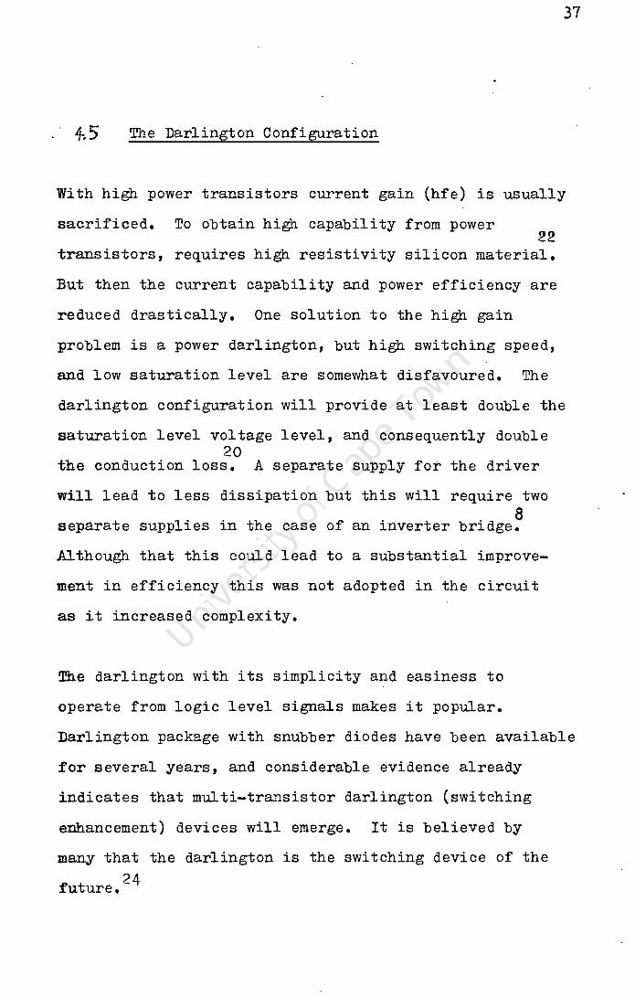
4-.5 The Darlington Configuration
With high power transistors current gain (hfe) is usually
sacrificed. To obtain high capability from power 22
transistors, requires high resistivity silicon material.
But then the current capability and power efficiency are
reduced drastically. One solution to the high gain
problem is a power darlington, but high switching speed,
and low saturation level are somewhat disfavoured. The
darlington configuration will provide at least double the
saturation level voltage level, and consequently double 20
the conduction loss. A separate supply for the driver
will lead to less dissipation but this will require two
separate supplies in the case of an inverter bridge~ Although that this could lead to a substantial improve
ment in efficiency this was not adopted in the circuit
as it increased complexity.
~e darlington with its simplicity and easiness to
operate from logic level signals makes it popular.
Darlington package with snubber diodes have been available
for several years, and considerable evidence already
indicates that multi-transistor darlington (switching
enhancement) devices will emerge. It is believed by
many that the darlington is the switching device of the
future. 24

4.0 Requirement Of The Transistor Bridge Diodes
For an induction load, the power factor is always lagging,
and therefore when the voltage is removed by switching off
a transistor an alternate path for the current must be
found. This is provided by the diodes. To prevent a hi&~
kickback voltage when the current commutates from the
transistor to the diode, it is essential that the transfer
occurs smoothly. When a step function of forward current
is applied, the voltage waveform appears differentiated,
as if the diode is inductive. Therefore, the forward
recovery time should be.at least as fast as the transistor
switch off time. This is fortunately normally the case as
d " d h f t h . d 1· t . ~5 1.0 es are muc as er t an trans1.stor ar 1.ng 011 pa1.rs.
Although the forward characteristics are important, reverse
recove.ry time is of utmost importance 0 When a diode is
conducting current in the forward direction and the
transistor in the same limb, but opposite side is switched
on, short circuit current will flow through the transistor
~.·the reverse direction of the diode, until the latter has -to
gone inAthe blocking state. Reverse-recovery time is a
measure of the commutation capability of a device to switch
from an on state to an off state. Charge stored in the
forward biased diode must be depleted, when the diode is
suddenly reverse biased. Therefore, it is essential that

the structure and supply inductance limits this peak
reverse current within the transistor current limit.
The diode also provides a current path when operating in
the regenerative mode and therefore must be able to
handle current requirement and the resulting power loss.
The diode used in the design of the inverter is the
Motarola MR702
39

Lt.7 3,19
The Loss Mechanism In Transistors
The power losses involved during the forward conduction
state of a transistor are simply equal to 2VceIm
(neglecting switching times) where Im is the motor phase
current. During switching the losses involved are not
so obvious. The energy dissipation in a switch
operati:~l, is Er"",VbImTr where Vb is the battery voltage - 2
and Tr is the rise time of the collector current. The
diode losses are small compared with other losses. When
the transistor is cut off, a high dI/dt is produced due
to the supply and structural inductance (Ls). The
following approximation can be done dIm/dt=Im/Tf the
ener~ expended Ef = (Vb+Ld~/dt)ImTf where Tf is the
fall time of the collector current. Hence
Ef -_ VbImTc + LsIm2
Th f f f 1 th 2 --z- ere ore or cyc es e power
loss is equal to 2VbIm+4(VbIm(Tr+Tf)+Lsrm2)f, since two 2 ~
transistors per path and two switch on and switch off for
one cycle.
The losses consist of three groups Wf=2VbIm, Wb =
4 (Vb Im ( Tc+Tf) f, 2
Wf is the forward conduction losses and is frequency
independent. These are minimised with a low Vce (sat).
40

41
Ws is the dissipation of the magnetic energy of the
structure and the supply. This term is independent of
the switching speed and is minimised by keeping the
structure inductance small by designing a compact struc-
ture •. The shape is also important and a c1.rcular one should 8
theoretically be best. It is also frequency dependent
and the same as the above is applied. As this term is
proportional to the current squarePit is vital to limit
the current switched on or off at anyone time. The
advantage of the interlacing is therefore of great
importance since only 1/8 of the total current is switched
at anyone time. Wb is the dissipation from the source
to the switch when switching ,2nd is minimised by a fast
switching time. This term is frequency dependent, and
therefore the frequency must be limited so as to optimise
'overall efficiency of inverter and motor. The above
losses were ... c~separated (see Appendix E).

CHAPTE~ V
THE LOGIC WHICH IMPLm';ENTS THE SWITCHING OF THE
.9 PR4.SE INTERLACED INVERTER
5;1, The Logic Controller
A brief summary of the logic which produces the switching
action of the interlaced 9 phase inverter is given. Each
section is given in block diagram form (see FIG .. S. I _ ',) and
is subsequently dealt with separately.
,5.1 01 Summary of Logic
The circuit basically consists of five blocks, an oscilla
tor, a Mis generator, a drvider, an 8/10 generator, three
shift regis_~ers and an output ploc}:
5.1.2 The Oscillator (F! 6. 5.2 )
Close loop development of the inverter drive in the presen-l:;
investigation was not contemplated. An ordinary bistable
was sufficient. An NE 555 I.C. wa~ found sufficiently
stable and 'adequate for the purpose. The frequency is
simply controlled by a variable reSistance.
S.l. 3. The MiS Generator ( F 16- 5,2 )
The oscillator output is fed to a binary up counter
(SN7493) which resets at the count of every 8 pulses.
The output of the counter is compared (SN7485) with a
preset (part in 8) mark-to-space ratio on switches. The
counter sets a flip flop at "0" and utays high until the

select chop frequ~ncy setee t . mark space ra ti 0
,I, II 1 ctock1
variab[~ mark-space 18 BIT oscilLator /' generator shift register /
I / Il
// /
select nb chop per cycle.
111 I ctock2 /
divider 18 BIT A:--
~ r---
~ 2/+;·· ....... ,256 r- I- +9 f-- shift register I....- . II I
, .... -I ' "
l
,.. T/O I clock 3 l.. L· Y
.It .., ::.. .,
e/10generator 18 BfT ,- I shif t regj star
III
FIGURE5.": BLOCK DIAGRAM OF TTL LOGI C CONTROLLER
:>
:>
~ ,,./
output btoc,t< .
~ VI

OSCILLATOR
NE 555
UP COUNTER : I ;1 COMPARATOR
(. I : - I
SN 7493 0 '''" \' a
SN 7485
FraURE 5.2 THE OSCfLLATOR AND THE MiS GENERATOR
+'"
1::/1 ~
B, ~
II \\.
1
..+:>
..+:>-

45
desired mark-to-space is counted. When A = B J the flip
flop is reset until the counter sets it again at the count
of 8 (or "0").
5.1.4 The Divider ( Fig 5.3 )
A pulse at 1/8 of the frequency of the oscillator is taken
from the counter of the Mis generator (SN7493) and divided
by 1, 2, 4, 8 ••• 256, depending where the output is taken
from the two 7493 I.C. The output of the latter goes to
a counter (SN7490) which resets at the count of 9 pulses
(i.e. when A and D are high). The C output is divided by
, two, by a flip flop.
- S.I.5. The 8/10 Generator (F /(7 5. t- )
The same pulse from the Mis generator co~~ter C output
is used. This goes through an up counter (SN7493) which
resets at th e count of 18. 'The reset pulse is derived
from the above at ~ider, through a monostable (SN74121) to
produce a short trigger pulse. The C output of the counter
which is only high for 8 pulses is in turn used to produce
a short trigger pulse (SN74121) to reset the flip flop
(SN7400). The flip flop is set by the trigger pulse
obtained from the dIvider, which occurs every 18 pulses.
The result is a pulse with a high for 8 pulses and a low
for 10, which is in step with the 9 high 9 low output of
the above divider.

46
'" C1
.... Q
M en ..:..:t
t'"
\11
...,. 0 ::
t--. 1( Z
;)-... \I'" If)
"-
c:t <t c:i:). " 0 0:: UJ 0 -> 0
UJ ::r: I-
('I')
en (t')
t:! en m t:!
z z ~
tI)!. tI) W
IX ::>
~ (!) ~~ ... -u..

..... nil .... ·_~F ... 1'" "0'-
J J'f 11
~ 1'0 .t I--.
\
7493 J~ ~14121
74121 ~ 0
I
FfGURE '5. 't THE 8/10 GENER ATOR
•• 2 9 '.. ..
~ 'f.! I " II
I) I 'f
D fS'
J 'f III
II
-=
II '" 3
,. \\
II
~ -l
5.1.6. The Shift Register ( FIG 5.5 ,)
The shift registers are 18 bit shift registers which
consist of 5 SN7495 I.C. each. They can be selected to
shift from left to right or right to left depending on
the state of the mode control. This determines the
direction of the motor. It must be noted that in the
third shift register the clock pulse is delayed by a
~onostable (~4121). This provides the required delay
mentioned in Section 2~3.
~.1. 7. The Output Block (. FIG 5.6 _) "
43
The output of the three shift registers are combined to
form the control for the 36 power transistors ,of the inter
laced inverter. The 9/9 output of the shift register 2 is
straight forward and control as such the PNP transistors.
Outputs of the shift register 1 and 3 are combined to form
the control of the NPN transistors. Basically it consists
of taking one of the 18 output of the shift register 1 and bA/£' C',c: '.J7/F7 R/C/fT.E~ #~'.a '--CJ"'.//.f//I///V./ Td..tFp1~
At first sight it would seem sufficient to obtain ,the
, required control pulses for interlacing by sirnpl;r inddlf'J6 \,
output 1, 2, 3 • • • 18 of shift register 1 with output
1, 2, -3 ••• 18 • • • of sh~ft register 3 respectively.
This however does no't produce a complete interlacine
logic as extra pulses occur when the sequence goes from

r the last output to the first output of the shift register.
This occurs because 18 is not divisible by 8 - therefore
some of the phases would experience a higher average M/S
than others. The problem was overcome by using·a data
selector which consists of two 7485 I.C. (see Diagram 5).
The idea is to detect when a discrepancy occurs and phase
shift the output for a period of time. In ~his manner
49
each phase experiences the same total amount of pulse widths.
The shift register and /the output block are shown in figure5.6.
A variable frequency oscillator determines the clock
frequency of the first stage (clock 1) - In Section 2 the
mark-space generator can produce eight discrete pulse
widths whose mark-to-space ratios are selected by binary
coded switches as desired (1/8, 2/8 .0 •• 8/8). The out
put of the mark-to-space generator is then fed to an 18 "-
bit shift register with 18 outputs. The clock is set by
the oscillator.
In Section 2 the oscillator frequency is divided by 8 " and subsequently by 2, 4, 8, 16, 32, 69, 128 or 256 as
selected. This output determines the clock frequency of
the second stage. The clock frequency is divided by 9
to produce a pulse which is on for 9 clock pulse and off
for 9 this determines the fundamental frequency of
the inverter and is fed into an 18 bit shift register.
cue I
1/ "\
1 --;o...j~N?lffiM G j" /I
.J
1 Cl.K _
" \" 2~'/' r /1 JJ I I
r--
eLk .J
'3" -r-l~NI~9561ci L
'--
II " J
I...---f---t-
/I 1/
r
a ....
SN74157 I
" "I Z, , ' ~; ~,
~~, J I-", ", ::> ~~ a.. I'll I-:f ~ :::l 17, 0 II
Jill ~
~+1 1-'
J j11i !l :\1
,I, il
I + 14'1 I i'~ ~: ,':: ; -~ !<! ,~
.. +.:.' j ,
;;'I'~b.' ------::,';1:1 '1'\::;: i Ilj' ,t,i ;0111 ,I.:
"i! Ii'~! ,\~;:I1Y II I:i "'" I'I'! .1 !.~ .11
PI! ,,'~ J!:., ,i", I ..
: 1111,
4tH I~ ---rT"TT'tT T-1
• ifl iii L_ - J==t~E I ~=----=~;~~~~=~3glfmEE
~~~ F J GURE5:6 T~;E SHI F T REGISTERS AND OUTPUT BLOCK
'-" o

5I
Section 3 produces a similar pulse as above (same fre
quency) but on for 8 clock pulse and off for 10. This is
again fed to an 18 bit shift register - the clock2_pulse
is shortened by n variab18 anolmt bct'l.·!ecn' 5-30 micro sccnnds
to produce the dalay nccos~ary' H~lGn "sto'Ppin!"!"., T"lis is t'10
requtrcd delay montion8d i~ sccti~n 3,3.

CHAPTER VI
DESIGN OF THE 9 PHASE MOTOR (B)
6.1 TORQUE REQUIREMENT
The main criteria of design was torque requirements,
especially stalling torque, as the project mainly
concerned itself in investigating a possible direct to
wheel motor. Results obtained from the 9 phase motor (A)J
which is described in Appendix ~ justified the design
and the construction of one of the two motors which is
to be directly coupled to the road wheel.
6.2 DESIGN OF STATOR CORE
.Alarge diameter at the air gap is essential to achieve
high torque, as the torque increases with the square
of the diameter for the same core stack length and
linearly with diameter for a same volume (i.e. approxi
mately the same iron weight). As the maximum electrical
loading and magnetic loading are restricted by losses,
thermal dissipation and material properties, a large
diameter is the most obvious answer to increase torque.
Nevertheless a large diameter increases the overhang
to active copper ratio as it implies a relatively small
stack length. Effort must therefore be made in the
52

53
winding design so as to keep this ratio at an acceptable level
(ie. many poles). Readily available laminations, with suitably
large diameter of a.245m at the air gap were chosen.
Assuming similar loading, as the'motor described in appendix
Fwhich gave us a force per unit area of 15900Nm/m2, the
stator core length (1) required to produce the desired torque
of 125Nm per motor (see Ap1)endixH) is : 1 = required area
radius XliX 2 .. 125
area =
1 -G.-2-45 x 0.1223 xTTx 15300
= 0.OB3 tr'I
torque 15300
A O.05m stack core was decided on as the weight of the motor
would become excessive. To retain the torque of 125ITm on start
the electrical loading will have to be increased to
65300 x 0.0~3 = 108400 ampere conductor/m 0.05
Such an electrical loading is rather high for an induction
motor. But considering that the maximum torque on stalling
is seldom required, it would be acceptable provided the
temperature of the winding is kept within its thermal limits
by the driver ~~ with the control.
-£'.3 "1' d' 1"\ • o ',; 1n 1ng ·)e81.",:n
The total ampere conductor to produce the required electrical
loading ~f 653')) arr.p conductor/m on starting is ;-
that is
10.3400 x 0.24 xu = 31730 ampere conductors
.91730 = 9031 ampere conductor/Ilhase. 9
I

Assuming all coils of each phase connected in series
and a maximum current of 25 amp. The numbe"r of
conductors per phase is 363 A large number of pole
decreases the overhang to active copper ratio as it
reduces the length of a coil pitch. However, since
many poles requires many separate windings and,
therefore increase the cos~)a practical number must
be decided upon. An 8 pole motor was chosen as it
lent itself best to the available laminationS
The number of turns per pole per phase (per winding)
is
= 22.7
MW-f'!f
22 turns was chosen in accord with 3.W.~.14 I'
wire
and the available area of the tooth gap.
The practical realization of an 8 pole, 9 phase winding
is shown in Figure6.I. The limitation to 36 slots by
the laminations which are readily available meant that
with a conventional arrangement there would be 4t coils
per pole for a double layer winding. These coils would
have to be equally distributed between the 9 phases
which were desired.
54

FIGURE 6.1
AN 8-POLE,9-priAS:S:. rnACTTONAL SLOT WIIlDING TN ':\6 SLOTS
Outer double layer coil span 1-5
H, H, 1",
All start on on l.h.s Phase connections ACEGJ on l.h.s.
All finishes nn r.h.s. Phase connections BDFH on r.h.s.
55

The average pitch is 4* slots per pole and the winding
is therefore essentially fractional. The number of
coils was increased to 72 by arranging for two double
layer windings, one with a pitch of 4 slots and the
other with 5 slots. Each phase has 8 coils with an
average pitch of 4* slots.
All the starts are brought out on the left hand side
of the motor and the finishes on the right hand side
to facilitate the interconnections. This results in
the termination of 5 phases on one side and 4 on the
other and allows the convenient connection to the
transistors mounted on the aluminium end shields.
see construction chapter 7
6 4 Maximum Speed at FullFlux •
2 Assuming an average flux density of 0,6 w/m. The
average voltage per phase is
Vph = n x 0,6 x Ux L
n = number of conductors in series per phase
v ~ velocity of air gap phase
L core stack length
With a maximum battery voltage Vb
56

V pha~e = Vb x 8/9 (1600 conduction angle)
11"= 8/9 Vp 22x2x8xO,6xO,05
IT=
or 0.11 Vb revolution/sec
Velocity at road surface with a~0.32m wheel diameter
.240 .1125
= 0 •. 6 f Vb km/h
x 3.6 km/h
with a maximum battery voltage of 60v the speed of the
57
motor is 397r.p.m., and the speed of the vehicle is 38.4km/h.
The inverter fundamental frequency is
\ O.llex 60 x 4 = 2005Hz.
It must be noted that the above calculations are based
on an average flux density of 0,6 W/m2 this is a
value normally used for sinusoidally distributed flux
and could be more as the flux has a square wave
distribution and the iron is used more evenly resulting
in a higher average flux density. I

r
Thickness of Yoke
Flux per pole on the basis of an average flux density 2 of 0,6 W/m •
Pole arc at air gap = 1fx.245 m . 8
58
If By = flux density in yoke, dy = yoke radial dimension
·0 6 • x 2"-
-dx .245 8
1 Xay
For a yoke flux density of 1.3 W/m2
dy = 0.6 x -tf x.245 1.3 x 16
= 0.022 m
The laminations used were 4 pole laminations with a
0.052m yoke thickness. The yoke thickness can therefore
be reduced to 0.022m for an 8 pole machine. The
laminations were cut to an hectoganol shape as it lent
itself best to the desired type of construction (see
Chapter VII Figure 7.1, 7.2, 7.3) •
....
Squirrel cage type, unskewed rotor with 32 slots.
DinelD.sions :-
Copper Bars : 0.006 x 0.04 x 0.05m
Copper Rings : outside diameter 0.0240m
inside diameter O.OI60m
thickness ; 0.006m

CHAPTER VII
CONSTRUCTION OF THE MOTOR-INVERTOR ASSEMBLY
'7.1 STATOR
The laminations are held together by bolts which run
through near the corners of the hectagonal shaped
lamination. They are also sandwiched between two
steel rings of O.6mm thickness. See Figure 7.1, 7.2,
7.3. Standard 4 pole laminations were used and cut
to an hectagonal shape with the yoke thickness required
for an 8 pole machine. The holes for the bolts were
drilled with great care. A special jig was made to
assure good alignment of all the stator laminations
of the core stack.
7.2 WINDING
The winding as described in Section 6.3 can be seen in
Figure 7.~ The interconnections between separate
windings were soldered together and insulated with
sleeves. Ten ends of five phases are brought out on , the one side and 8 ends of the remaining 4 phases are
brought out on the other side.
59

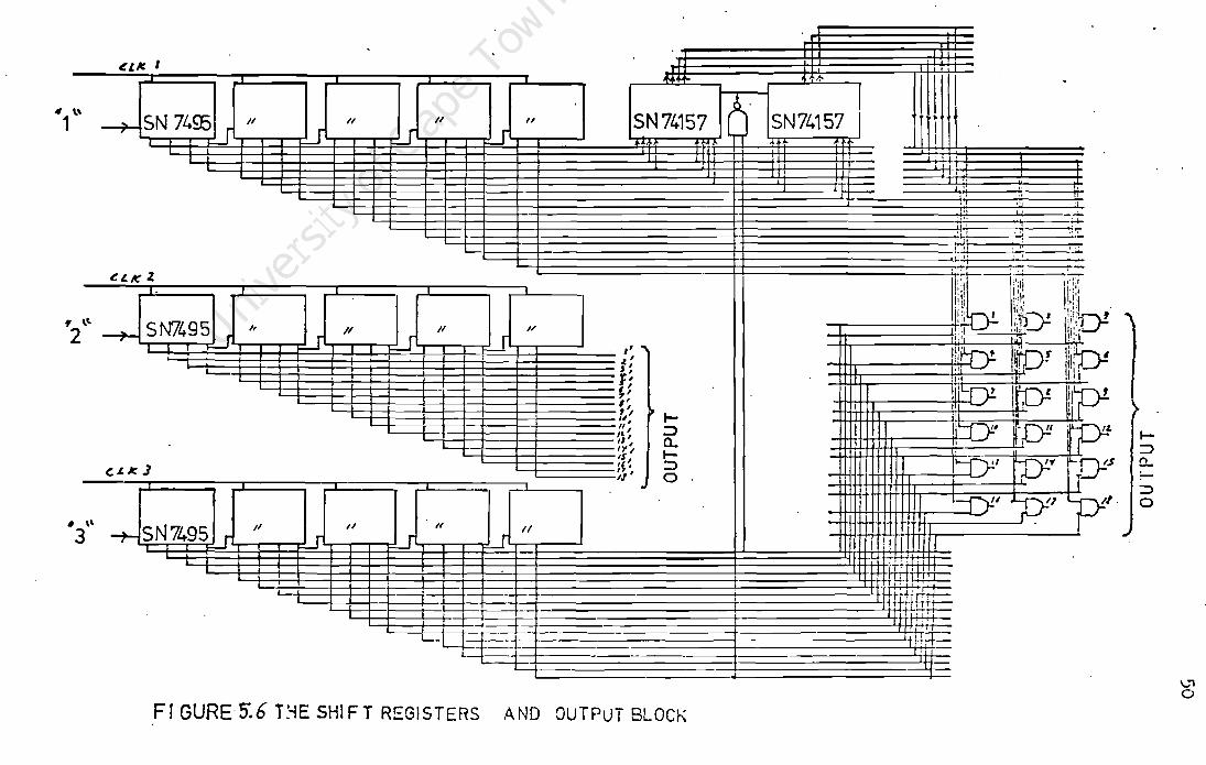
?iflirG 7. 1
stc. tor laninaticn
rotor ! c.;.ina ticn
eno nlatG ul thout tr3l1~lstors
, _ I ' Stat:Jr and r otor la!:inat i ons·, stator cor e , notor. end plata
'" o
61
!i 0 .c • g .. ~ • .:l ~ .... • §
'" ~ :: " u ~
• • " 0 " • u . ~ "
'" 0
• h U
0- 0 • ~ ~ .... h
• t .... • 0
~ 0 ~ ~
" ~ ~ • '" .. "

Closo up vio,"" of stator cor~ stack
Sl.3tOl' core sbclo: \11th utncling

7.3 INVERTER
The 9 phase induction motor and it's inverter are part
of the same assembly. The inverter transistors are
mounted on the end plates of the motor which carries -
the bearings. Figure 7.S shows the outside of the
transistor carrying end plates. The 2N3055 and
2N2955 transistors can be seen. The positive rail is
a copper bar of 2Omm2 and the end plate itself is the
negative supply rail. A printed circuit board links
the base of the driver transistor with a terminal which
brings in the biasing signals from the interface stage.
On Figure7.6, the inside of the end plates can be seen,
the MJ802 and MJ4502 power transistors are shown. The
power transistors leads run through the end plate and
are directly connected to their respective transistors
which are mounted directly on the other side as seen
in Figure 7.5 The power transistors are electrically
insulated from the end plate with low thermal resistance
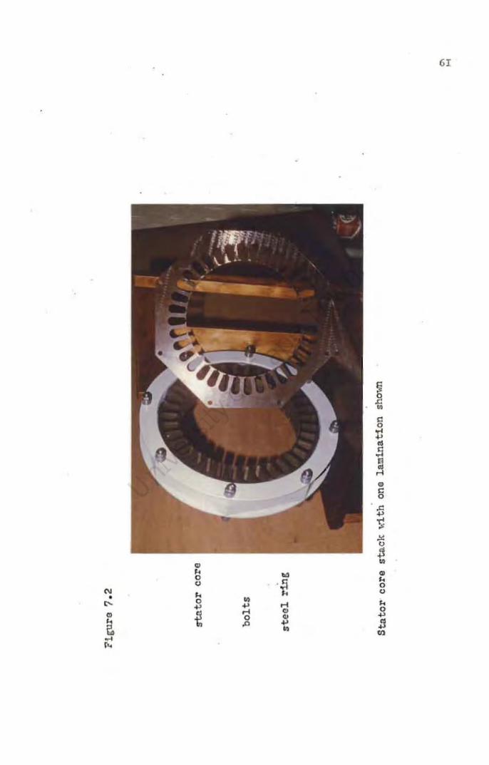
berylium washers. Figure"?! shows the half assembled
motor-inverter. The end plates are connected to the
end plates by pillars which are thread~d directly into
the stator bolts, see Figure 7.'9
The final assembly is seen in Figure 7;8 The mul ticore
ribbon type leads which connect the terminal of the
63

Figure 7. 5
p=1::.tcd cu1rcu:1.t board
t er=1nal
External s ide of end plate
r;Pirdr1ver transi stor ~
PHPd rlver tra."ls1stor
pos~t1ve s~~~17 Cop!'ler bar
'" ~

Figura 7. 6
r~pn pot-!er tra::ls1stor Fir? tlO1;,er trans1sto
H:!lf asse:n.bled rtotor and inside vieu of one ot the end plates
'" ~
66
F1euro
Figure 7. 8
COr.'LDlctcd r.n tol·- invc.:rtcr n::;oolilbly

printed circuit boards to the interface stage
(Appendix E) can be seen.
The' motor \'Ta.5 mounted to a dynamometer for testing' and
evaluation porpose see figure 7.10
Figure 7.9
Connection be~'Teen stator core and end plate
,
67

~~tor and dynaMo~Qter .

69 CHAPTlm VIII ....
RESULTS OJ.!"' THE: 9 PHASE INTERLACED INVERTER FED INDUCTION r,':O-rOR
8.1 Stalling Torque
The maximum stalling torque was recorded for an approximate
fundamental frequency of 1Hz. Results were taken for different
battery voltages and ~T/S ratios and are tabulated in table I.
TABLE 1 . ,
~ 1 2 3 4 5 6 7 8
torque Nm 0 8 27 37 _42 57 65 70 supply amr 0 6 16 32 44 56 70 lOS
--
~ I 2 3 4 5 6 7 8
torque Nm 0 30 57 70 84 91 100 110 , supply arrq: 2 12 28 44 70 90 .. 110 170
~ 46V 1 2 3 4 5 6 7 8
torque Nm 23 54 70 91 107 - - -supply amp 5 17 36 60 80 - - -
~ ,
60V 1 2 3 4 5 6 7 8 .
torque Nm 0 70 91 - - - - -supply amp 6 22 48 " - - - - -
The torque per amp per phase was found to be 5.9 Nm/amp/phase
on average. In the jesign the desired torque of 125 ~fm was to
be obtained at 25 amps per phase, this is 125 = 5 Nrn/amp/phase • 25
The torque obtained is higher than this which su~gests that
the flux density is above the assumed density of 0.6 :;1b/m2 •

70
The same torque can be obtained by either a low battery voltage
at a high supply current with an high Mis ratio, or a high volt
age and a low supply current wi+h a low Mis. For example see
Table I, 70 Nm can be obtained at 16v with full Mis with the
resulting current of I05amps, 30v with ~ Mis with 44amps, 46v
with ~ Mis with 33amps, or 60v with ~ with 22amps only. Hence
full torque can be obtainea with a reduced Mis with a relatively
small supply current. The battery supply current was found to have
a maximum ripple of 15%. Therefore the R.M.S. current of such a
drive is virtually the average current. It can be said that the
interlaced inverter acts like a direct current transformer.
3.2 l\'~aR;netizing Curves
The Magnetizing characteristics for different frequencies
were obtained by driving the motor so as to obtain a zero
slip frequency. See figure 8.1. Saturation is seen to occur
in the region of a battery voltage to frequency ratio of 2.4
(except for very low frequencies).\At the maximum battery
voltage of 60 volts, the saturation frequency is aoout 20Hz.
This is less than the predicted frequency of 26Hz. (see section
6.4). This suggests that the flux density is higher than the
assumed 0.6Wb/m2 •
8.3 Load test at full flux.
To operate an induction machine at a good efficiency, the machine
must be properly fluxed. If insufficiently fluxed it will suffer
" high slip and if excessively fluxed it will have high iron losses ,
~. and high magnetizing currents. Tests were conducted at 12.5Hz for
[ 3 different voltages in the region of saturation, namely at 24,)0
and 36 battery volts. The torque efficiency and supply current

Go I)
td ~ 5011 1-3 ~ t.tj ::0 ~
~ 0 'tOll t-i 1-3 > 'Il L-:l
..-..... <. 3tN 0 t-i 1--:3 C/J '-'
2,01/
I
!OV 1
/
./
f f
II /
10 U? J()
SUPPLY CURRENT (AMPS)
Figure g.I !I'agnetizing Curves for 9 Phase Inverter Fed r,:otor
12.$ t+i.
'10
"
i,ZS' If 2-
.:J,IZr H 5"
b. 75' ttJ,.
-....J H

r , 72
obtained is shown in figures8.2,8.3 and 8.4. The maximum efficiency
recorded for the 3 tests ~~s 62.510 at 30 volt battery voltage
with a slip of 8%. At 36 volt; the maximum efficiency decreases
slightly to 57.5~ at a% slip.It can also be seen that to obtain
say 30 Nm the efficiency is 62.3% for a slip of 8% at 30 volts
and only 52% for a slip of 4~ at 36 volts. On the other hand 3gNm
is obtained at a slip of I6~ for 30 volts and 5710 at a slip of
7.2~ for 36 volts. A large value of slip produces high currents
resulting in high copper losses, while too large a value of flux
wilt cause saturation, with the resulting increase in iron losses
and magnetizing current. To obtain maximum efficiency for a
desired torque at a certain speed, the inverter frequency m~st
be set to provide the right slip frequency -.and the inverter vol t
age for the right flux density.A point to point adjustment of
frequency and voltage would provide optimum efficiency through
out the speed range. The information could be obtained from
practical tests. 1 and stored in a.n aru>ropria te memory. A calcul-
ation method would be difficult as battery and inverter regulat
ion would introduce another variable in the classical method
of induction motor theory. A more simple method is to operate
at constant slip frequency corresponding to maximum efficiency
at rated load. Little efficiency and performance would be
sacrificed.
8.4 Load teets for variable frequency
Torque verses speed characteristics were recorded on an x y
recorder for 6,12.5,25,37.5 and 50 Hz inverter fundamental
frequencies. The voltage v~s varied in steps of 6 volts up to
60 volts. The results are given in figure 8.5 • ds torques above

-
.f ( v
~ I' P L I
~ 5 1 " f • AI AI
I' (.
V 100 100
So go
'0 '0
'f~ YI
.20 1.11
7 C1 .t
~ £ H'11I
Sf) .
Yo
,-~ ,,-', . . ,," \.
J3 ~l'FFlClEAlC.Y I I
" I
Jo ,
L!,.~ I ,..A!J- \ I
~ \~ ~ \--r~Mt;II' ~ "QPJ'Lf C.ORREA'1
20
/0
, o 37S 'f.P.M.
Figure 8.2 Torque, Efficiency, Supply Current VERSES Speed for
2'~ Volt, Full r,:/s at I2.5Hz.
...... v.
f

E .,.
.f f) () F I? P F
160 q Sf) , , '''0 I L C 1/
Y J J;
F 1J".,. /I
P 10 1 YII M ID
-~0. ,
\ \..- TtJA.q7vE ! J
('{J -I
VQ -I
.l.d .j
,
\9\ It> ~ .1" ~
,t!' \ \ _ EFFI< I If N<- \j , I
I ~~ \, \ :
~
9~ prJ ~ 20 ~ .
I', ~Jv'P/.y "iMJO
v.-20 -I 'I?
115 R .P. M • .. Figure 3.3 Torque, Efficiency, Supply Current VERSES Speed for
30 Volt, Full MiS' at 12.5Hz.
-.1 ->

S t /I /flf) F /(10
f f p
, '-
l- I
Y .If) E II Jo
C. t. V Y ~ 11 / f (f) • Itl }J
7
y" j y., -l
20 _I 2f) -I
---~ .Af)--r -- \ () So ~ R 4> \
\' "'Olf/lle ()
.t ~ AIM YO \ \
~ IClPP~Y G (/"fRENt :10 -0-----< \
/~, ,HILlEN'" / \ ,,-
:}o ~ /./ 6\ k ~ \i / ~j
If) ~ ~
Figure 8.4 TorClue, Efficiency, Supply Current VERSES Speed
for 36 Volt, Full 1vr/S at I2.5Hz.
-..J \J1

r 0 R p (/
E SD
(,vqn)
If~ J
30 J
10 1
/fl j
l.Yv'...1 J(V \ I()V.
\ S"yv Jol/
If"
1\ I y/V,
s't
Ifl
12. II l.f2
I2V
InS" f.il.$"
till
37S 12SII}
7S"()
2.SIf.J. J 7,S' "l-/5"Ot:7 R.P.M. speed SOH~ ·Hz inverter fre1uency
Fi~~re 8.5 Torque, Speed Characteristics for various Frequencies
and Voltages at Full N/ " ~

55Nm could not be recorded with the available dynamometer,
the voltage test for higher voltage at low frequency could not
be obtained. Full stalling torques were however obtained with
71
a spring balance. From the mabnetizing curve it was establish
ed that the saturation frequency for 60 volts is about 20Hz. As
the frequency is increased above 20Hz the machine became under
fluxed as the voltage cannot be raised any more. The fluy. "'-decreases linearly with the frequency and the current.The maximum
torque also decreases. The flux and the current decrease linearly
with frequency. Hence the maximum torque is inversely proport
ional to the frequen~y2
The corresponding road speed for a 0.32m wheel diameter at 20Hz
is 18,3 lan/h. This also corresponds to peak power.
8.5 Load Tests when Chopping
The chopping frequency must be a multiple of 16 times the
inverter fundamental frequency, by virtue of the constraints
of the.logic of the interlaced inverter. The chopping frequencies
which are available at 12.5Hz fundamental frequency are :- 200,
400, 800, 1600, • • • • The chopping frequency of 800 v~s used
as it was found to give the most favourable performances. Load
tests at 48 battery voltage, 5/8M/s ratio were performed (see
fig 8.6) so as to compare them with the equivalent of 30 volt
at full m/s results obtained in figure 8.3. The obtained torque
is somewhat higher than that at 30 volt full Mis and lies
between the result obtained for 30 volt and 36 volt full rr.ls.
This is due to the fact that the volt drop due to r~gulation of
the supply and inverter, is more pronounced for 30 volts, full
Mis than 41 volts 513 Mis as it's supply current is hieher. The
~ ~ j ~ '" F F IOf) I t I
~ 1·1 f II ~ tf) Y , 0
,,, J If) J
~- f/,
2tJ 1(1 _
r f)
~ q $"'tJ
V E tim
~(I
J()
lO.
111
'~ \ ....... r()A(f'tlE
o \ \ \ \ I
,i1]\ 1\ epF/tll!g~V " \
P ,
~ .rV,,"'y t-VlfAliAl7
&.\ I ,\
I
J 7 S R. P.M,
Figure 8.6 Torque t Efficiency, Supply Curren't VERSES Speed
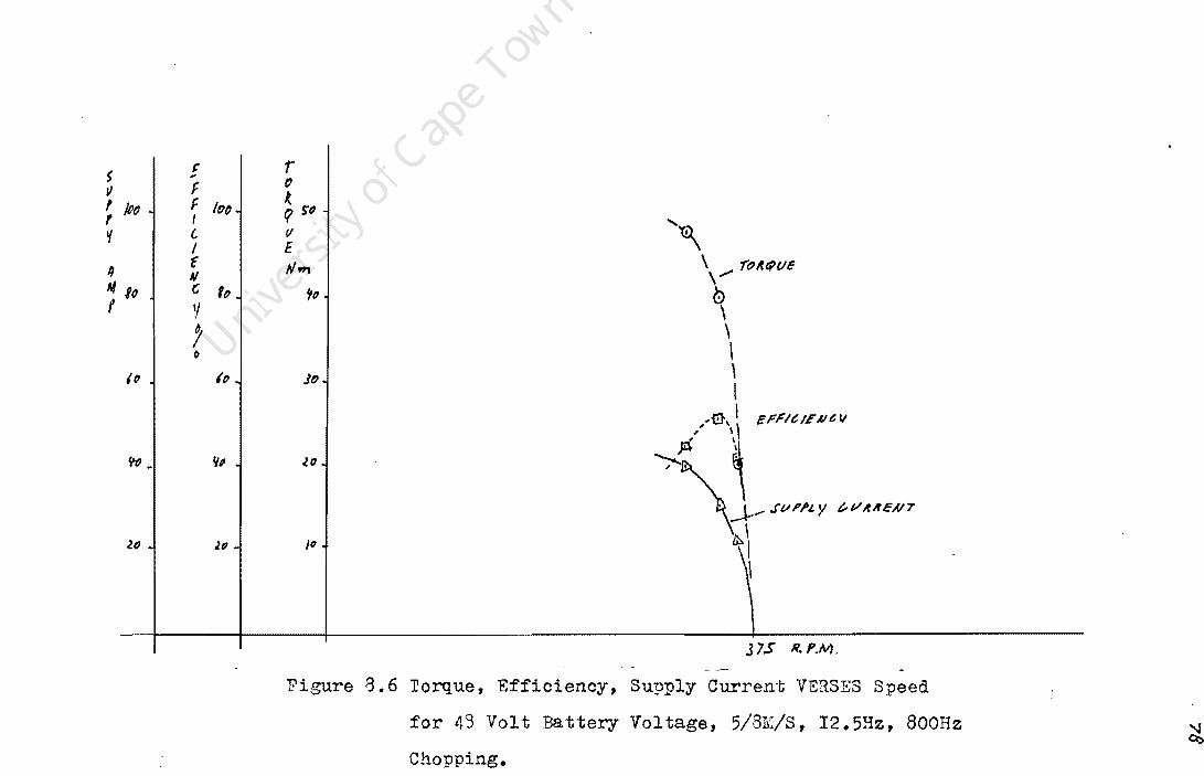
for 43 Volt Battery Voltage, 5/8K/S, 12.5Hz, 800Hz
Chopping. ~

79
same can be observed. for 36 volts at 5/3 Mis (see fig 8.7) and
24 volts at full Mis (see fig 8.2). The difference in efficiency
between the two modes is about 2%. This is accounted for by the
switching losses and the effect of ripple phase current due to
the chopping frequency.
8.6 3 Phase sinusoidal Test
The 9 phases were cumbined so as to produce a 3 phase motor.
Three of the phases were connected in series to obtain one phase.
Tests were carried out to enable some comparisons between the
efficiency of the motor when 3 phase connected, sinusoidally
fed, and the efficiency of the 9 phase induction motor. The tests, (
were superficial and approximate as the motor and inverter will
need further alterations. A brief attempt was made at comparing
the efficiency at 30 volts full Mis, 12.5 Hz and the equivalent
average voltage per conductor when ~pplied at 75 volts and
12.5 Hz for the 3 phase motor. The characteristics of the 3 phase
motor were obtained at 50 Hz and the characteristics calculated
for 12.5 Hz operation (see appendix H). A maximum efficiency
of 75% was calculated in the case of the 3 phase motor when
running at 12.5 Hz and 75 volts. Vlhen comparelwi th the overall
maximum efficiency of 62.5% obtained from the 9 phase inverter
fed motorJthe efficiency is appreciably less. If the inverter
losses are subtracted then the efficiency of the 9 phase inverter
fed motor is 67~. The difference of g~ could be attributed to
increased copper losses due to the substantial phase current ripPlE
experienced with the present 9 phase inverter fed motor.
The low efficiencies at 12. 5Hz are to be expected as the copper 1"os8
es are of importance at low frequencies, It was unfortunate that
the motor could not be properly fluxed for frequencies over 20Hz

$ If p P L V /QO I
II M
P 10
10
to
2.f)
! f F I C I(}(J
I t I.J C.
Y (0
! ,
'0
~o
.lo
..,. o ~
p V Sf) E
}1m
'10
Jo
lo
... 1':1., ..... l:I l , . , .
_r- , ..... (J) ..... ,.' '\ t.- En/(:. , E)/C. y
, I . ~ , 0' " \ fir .s f
~ \~ 7'ollqvE
~\ '
~l t SVI'PLY ~(/lll?elJr
/11 _
e
~
Figure 8.7 Torque, Effioienoy, Supply Current of 9 Phase
Interlaoed ~otor for 36 Volt Battery Voltage and
5/3 n:/S, I2.5Hz, 800Hz Chopping.
>J)
o
81
especially when considering that the maximum efficiency of 89~~
was measured when running the motor on 3 phase at 250 volts and
50 Hz.
8.7 Oscillograms.
Oscillograms of phase voltage, phase current and supply current
for different opera.tions are shown in figures :- 9.8, 8.9, 8.10
and 8.11. The phase current and supply currents were monitored
with hall effect transducers. From these oscillograms it is
noticed that the voltage waVe form has virtually no voltage
peaks oVer and above the battery voltage. Thereforethe transi
stors can be effectively used at relatively high voltage compared
with normal types of choppers (ie 60 volts for a VCEO max.
of 90 volts). The phase current unfortunately has pronounced
ripples. When comparing with the smooth ~hase curre~t obtained
with the 9 phase motor (A) of appendix H the difference is disturb
ing. Further investigation will be carried out so e.s to obta.in
a smoother phase current. A probable answer is t~at the present
motor is unskewed while the motor of appendix H is skewed.
Fractional winding, and the fact that the number of slots per
pole (4t) is not an integral number should have reduced the
effect of slot harmonics but is not suffjcient.
8.8 Proposed Modification to Motor
The torques measured with the present motor at different
frequencies for maximum voltage (shown in figure 3.5) are
replotted verses vehicle speed when using a 32cm wheel diameter.
These are shown in figure 9.12 and compared with the desired
torque of figure 7.3 of apnendix G. The maximum desired stalling
torques were achieved but unfortunately the torque drops quicl(ly
with speed as the motor becomes underfluxed. The motor will be
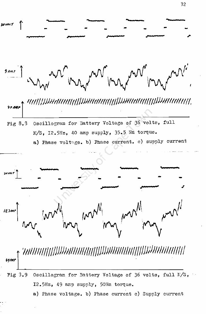
12
- ,... "" • ..... d • -. •
J(J~'T t - - - - - - - --. ...... - ".,..", •• 11 • F • ~ •• .'ft .. ~
I
tlAIII'I /111111 /1Jl/tlllllll I II 1IIIIIIfllllll I II 1/)111111/11111 111/11111111111111.
Fig 8.8 Oscillogram for Battery Voltage of 36 volts, full
Mis, 12.5Hz, 40 amp supply, 35.5 Nm torque.
s) Phase volt3ge. b) Phase current. c) supply current
'Jr ........ •
- - - - - - - -Zbt A'" ..r b. d .. ' b b b'" .,.. ..-
.$Allf I '/~/II II/II III IllJJII//11I /11111 II IlllJIII/11I / /111 II IIMJ II III/ /1111111
Fig 3.9 Oscillogram for Battery Voltage of 36 volts, full l;;/s, '.
12.5Hz, 49 amp supply, 50Nm torque.
a) Phase voltage. b) Phase current c) Supply current

33
. •••••••••••••••••••••••••••• ~ t ••••••••••••••••••••••••••••• ___. ; ........ a:.)
...,." ...... ...
S.,,",,p i
IFig 8.IO oscillogram for Battery Voltage of 36 volt,6/8 Mis, ; I2.5 Hz, 30 amp supply,25 Nm torque. ! ajPhase voltage.b)Phase current c)Supply current
r .. --_ .... w - "V-.. we_
H Vtn T .. _ ••••••• - •• _. ______ --:_. ____ •• _ •• _ ••••••••••••••• 11)
,. .... , •• ,1A
-• ; I " ." " I., , . .• :: ,. I ' j '/ ) . . .
I I" i/' tl tllilil-Illi llol·~;,~/:I.!f·J! l/~,lil,:/·lll·/i·i;l/ , - .. " ,. , " r. ~ . .. c...
30M,. 6-L----------------------------------------____________________________ ~
Fig 8. II Oscillogram for Battery Voltage of 43 volts, 5/3 II/S,
I2.5Hz, 300Hz choppinG, 30 anp supply, 40l'i!m torque.
a)Phase voltage b) Phase current c) Supply current

34
modified by reconnecting the winding so that there will be 2
parallel paths per phase (ie half the conductors in series per phase
Newly available and cheap Darlington transistor packages MJIOI5
and MJIOI6 (30 amp rating I20 volt VCEO) will replaC8 the present
power transistor, driver and freewheeling diode. The battery
supply voltage will be raised from 60 to 90volts. The result
will be that the torque obtained will be 2.25 (ie(90/60)2) times
as much and at twice the speed. The expected torque is shown
in figure 8. I2. To maintain I25Nmon stalli'1.g the numbers of
transistors will be doubled up. Each of the 9 phases will. consist
o~ two parallel windings each connected to a single phase
inverter. The two single phase inverters will be controlled
simultaneously by the Present logic. Although the numbers of
transistors will be doubled up the Darlington single package
transistor, which replaces the power transistor, driver and
£reewheeling diode, wil~ender the construction less complicated.
Also it is hoped that more powerful, cheap transistors will
enable reduction in the numbers of required transistJrs.
More investigation of the motor design will be carried out to
improve the efficiency, simplicity and reduce ·costs.
The logic ~ill have to be developed to control the motor in a
closed loop so as to obtain efficient and flexible operation
from the accelerator and brake pedals.
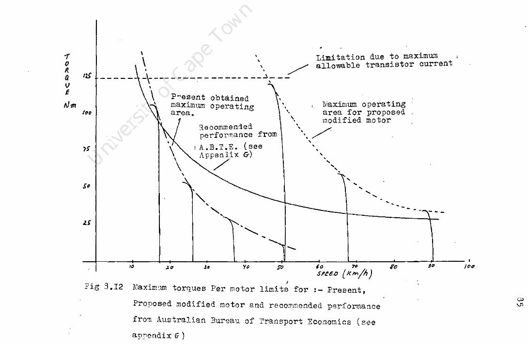
\
\ ' l
Limitation due to maximum allowable transistor current
"1 o ~ Q 11$ ... ____ _ -\- --- - - '../
__ :- _________ .J._ /'
\ ' --V E
Nm ItItI
)$
So
.z.r
P~esent obtained maximum operating
,
~
:i. e cOrrL.llencl ed performance from
I A. B. T. E. (see Appenlix 6-)
/
"- ...
" ... ............... ...
, ". '.
""'-
IY.1aximum operating area for proposed modified motor
\". /" • ....
... " .... ..
" " ... .. " .... ....
..... ..... ...
""' ..........
I I I I I U I I I ,I, ,,, ,HI Jo 'If) StJ 10 ,.() 1'0 ,Ia lot?
S,~c/) {/( min) I
Pig 3. 12 l\ja.xim~.lm torques Per motor limits for : - Present,
Proposed modified motor and recommended performance
from Australian Bureau of 'rransport EcoZlomics (see
appendix G)
Q;)
\J1

Conclusion
The project has suceeded in producing a viable drive with very
high stalling torques enabling direct couplin~ to the wheel. rhe
novel construction adopted has proved to be a success and has set
the foundation for further improvements towards an economical
battery operated motor.
The method of interlacing between the phases has produced
numerous advantages, namely :-
I) Continuity of the supply current.
2)Suppression of induced voltages due to supply inductance when
chopper modulating,
3) D.C. transformer action of inverter enabling high torques
with little current demand on the supply battery.
4) Reduction of switching losses due to stored magnetic energy
when chopper modulating.
The multiplicty of phases has enabled high utilisation of the
transistors.
It Vias unfortunate that the motor could not be properly fluxed
at higher speeds, therefore no impressive efficiencies were reco
rded. However with future modifications and investigations
there are no reasons to believe that overall efficiencies up to
90% should not be achei ved vIi th a direct to wheel drive for a
battery vehicle.

APPENDIX A
Tests to measure the frictional losses of the differen-
tial on the melex battery car were made. The series
D.C. motor is coupled to the differential with a worm
type gear. The motor is rated at 36\(, 57 amp', 2.1 h.p.
at 2 800 r.p.m. The motor and differential assembly
were driven from the wheel si~e by an auxiliary drive
through a system of pulleys. The frictional torque
of the differential and bearings was measured and is
shown on Figure A .. l.
Figure A.l
WIt,'S
;3?"O. pouer
·loc/)o
/""0
pm.,rer (').
c ItJ«J 1CCc 3 ClOO "I""" If P,411
Output pm'lor and friction loss of melex notor and
differential assembly
At~oninal output of 1 580w the losses amount to as
much as 20%. The differential is no doubt a very "
inefficient part of an electric vehicle. However,
this type of transmission (worm gear) is very
inefficient and would not normally be used in an
electrical passenger car.
realistic figure.
10% loss would be a more
87

APPENDIX :g
17 HARMONIC CONTENT OF VOLTAGE WAVEFORM .
The harmonic content of the voltage waveform of the single
phase full bridge inverter can be expressed as a function
of the conduction angle
"fa - :b) = ~ An cos nwt n = 1,3,5
An = -if Vca - b) cos DJt d/wt
\.(a - b) = Va for 0 (wt<. Y \!a - b) = 0 for Y <w.J~ < 11;2
An = 4/11 .1" 'VB cos IJtjJt d/wt
= 4,f( v; ESinnn til: = 4 Vs n 7T sin n y
Ila - b)';' ~ ! Vo/sin n y }/cos nw~l n= 1,3,5 ••••
4 \/6 = n7T sin nY V(a - 1) {n, m}
The maximUm value of the fundamental component occurs
when Y = 71/2 or Va - b is a square wave, and is
Va - b (l,m)j = )'~%
In the particular application used
83

the variation of the fundamental and harmonic content with
conduction angle is given in Figure 7.1.
Figure .B.l
p.u. V o '.ro L T
" 6 t 0.75
" M P .so L I T IJ Il .2.5 t
conduction «- angle:
~.:::--- ...... ........... , " " "-, , , ,
\ , \ ,
\ \
\ \ \ \
\ ,
\ 3rd harmonic \
\. \ \ \ \ ;th harr.l{'nic ;' ,... \ \ / , -'\--- . / \ .' , .....
\ ."...... .." ..... \ ," \ .~, / ,.' ",' \ X I
" ,.' \ / \\ ,I' \/ \.f \/
• 'l , .X- ".10 ,
to' 90' Il() 0 ISo/1
Chnracteristic sho,v.rng the voltage out!,ut harmonic content'" for a quasi-square voltage ,·ruvcform for different conduction angle
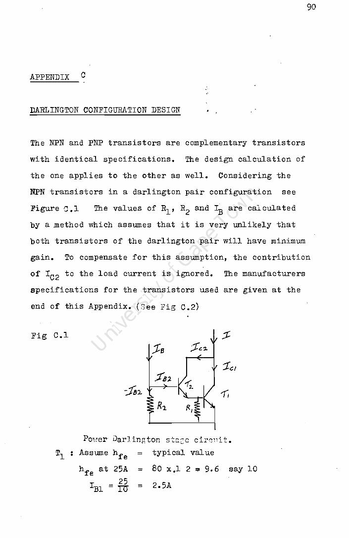
90
APPENDIX C
DARLINGTON CONFIGURATION DESIGN
The NPN and PNP transistors are complementary transistors
with identical specifications. The design calculation of
the one applies to the other as well. Considering the
NPN transistors in a darlington pair configuration see
Figure C.l The values of Rl , R2 and IB are calculated
by a method which assumes that it is very unlikely that
both transistors of the darlington pair will have minimum
gain. To compensate for this assumption, the contribution
of IC2 to the load current is ignored. The manufacturers
specifications for the transistors used are given at the
end of this Appendix. (See Fig C.2)
Fig C.l
Tl • Assume hfe = typical value •
hfe at 25A = 80 x.l 2 :;z 9.6 say 10
25 2.5A IBI = ro =

HI and R2 are to enable quick removal of charges stored
in the depletion layer, when the transistor is switched
off. The value of IBI_/IB depends on design requirement.
It was found that IBl_ ~ 0.12
off time (+lOf s)
lEI gave adequate switch
VBEl(sat) 1.6 HI = Oo15IBl = .12x2.5
IBl
_ = 0.12 x 2.5 = 0.3A
IC2 = 2.5 + 0.3 = 2.8A
T2 h fe at 2.8 amp = ! 40 = 20
I B2 • ~ = 140 mA
VBE2(sat)+ VBEl(sat) = 0.12 x 0140 =
= 503.fl..
106 + 1.1 = 166 fl-0.12x.140
= .140 + 0.016 = .156A = 156 rnA
91

92
I: •
J
• ! IH il H u n
I I ! !! i ~ ~
i <Of $I: J!: i I l! ~
! ~ ~ . ::: r
I ,;. S
t
.. • .2
~ ! J .- J I ~ .. !
;. " " ;---~ ~ I -I
• > > ~. ... III
~
iii 'I · 11 · I I ' .
11 ' .f ~ :: -J.!
c l ; .. ~ · : ,If
I II -AI I: i! j r J ~ , ;; • • U
8 i 1 · 2
:! % II
' ,
,. Il !I
:! •••

93
APPEm)IX D . _.l.
InTERFACE B3THESH ;)A3LINGTOlT PAI]S AND TTL LOGIC CON'r';{OLLER.
The" interface circuits' provtde" the tie bet",een the TTL logic
and" the pOHer D.erlington transi~tors-
The NPN ~nd PNP earlington pairs are controlled fro:'! the lo(!ic
revel" as shnvm in Figure 7.3.
Figure D.I
Logic" s':f;age
Interface stage
I
I +&OV
• ~ ~ _ _. POl'Ter stage . . .. "
•
pr:rp 'n01·rcr transistor I darlington pair . ,
I----I'l to phase ",inding
,.-- -..
0-',....1;----.....1...---1:- ""_~----H.W---i-K... . NPH POller transistor
darlington pair"
• . " t
.I--=~-•
Cheap transistors T3, T4, T5 are used to interface. T3,
T4 are MPS A06 a NPN transistor and T4 a MPS 56 a PNP
transistor. With this circuit both positive and negative
rai~are controlled from the same voltage level. T3
emitter is not connected to ground but to the logic gate
of the opposite leg. This provides effective interioc1ting-
to prevent both legs coming on simultaneously, in the case
of b~t'1 lor.ic gates s,'litc'~ing on due to noise or maJfunction
of the controller. T3 can onlv be biased if , :md only if", gP.lte

. { is "off". The applied logic signal of gate I can only
return to ground through gate 1. See Figure D.2,
FIGURE '0.2 - .. - fill" _ • _ .. __ ..... __ • __ .. .. • -. .. .. .. .. ..... ;
TTL GATE is --~--------.-~~
" ---
. ....... ---_ ............. _.- .. _ ... Internal cnil'cuit of TTL gate
'1'he interface stage bet~'Teen the logic stage and tho pm-Tar
stage can be seen on the left hem:) side of fi;',ure D.3
'1bis interface sta::o ~as also the necessnry torr:innIs to
operate a second identical Dotor.
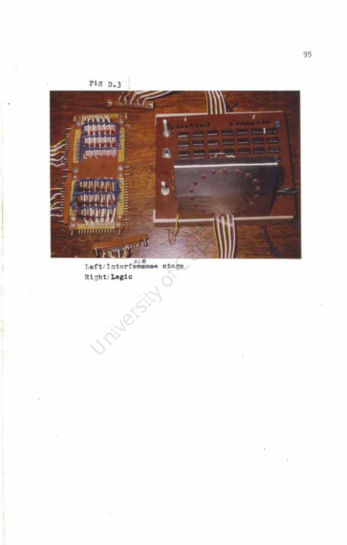
95
Fig D. 3
stage
Ri s bt :LGg1c

96
APPENDIX E
The losses involved in the switches for a particular phase
where measured with two wattmeters of an accuracy of 5%
up to 400 Hz. Although higher frequency components are
present in the quasi-square voltage waveforms and the
non-sinusoidal current, it was found to give adequate
results to be able to observe how different parameters
affect the losses. Results were obtained driving a
resistive and inductive load, and found to differ little.
Hence Graph I and II which were taken for resistive load
are applicable in the case of motors. The losses were
measured for different frequencies, voltages and currents , -
and are summarised in FigUres E.l and E.2. ,
Graph I illustrates how the dynamic losses increase
linearly with frequency for a constant voltage and current.
One can attempt to separate the last two te'rms (see Chapter
3.6) by studying the graphs. Graph I indicates that at
low voltages the increase in loss is minimal with frequency
increase. Therefore, the term which is voltage independent
can only be very small. It can be ignored provided the
current is low, as it obeys the square law. This is indeed
the case in the 9 phase interlaces inverter where only 1/9
of the total amount of current is ever switched at any
particular time. The VbIm(Ir+It)f, term becomes significant 2

f [
r ~.
nt hiC;h frequency as it is linearly proportional to
frequency. Since motor losDes due to ripple current
decrease with frequency an optimum chopping frequency
exists.
97
Fig E.1 Variation of switchinr, losses wi th frequency nnd vol tnr;e with on averaee Gurrcnt of 5 amps and a quo.si-nquo.rc voltage wavcfo'rm of 1600 conduction angle in ~ tranointor inverter
. i .-• .. i I·: .. ~ .• '."! • 3(). t. . . . .. .... -_ ... _:.-- •. - .. ~. __ ... - ...... - ... - ................ -- -1·· -_ .. __ ._ .. _.- .. .. I " " • . I .j .
I .;. ! . ··1 . \ ." . 1;· . I"';· .1,: ..! .. i . .; ! ;..! . • I' I . , '1-..:..-7.----1. ~ . ..--. --"';'--'r'--T' .. -.--..... : .
• ' j ........... : . . I..... !. .•. i. .. i ! I ., . ,
. I' , ·1\YATT LOSS. 20- -.-. --. - •... .;. .. --. - 0- •• Dynarriic t .';.. ! I . V I . . • 240 losses , .. ." • . I ~ t' . i" 'j . ,.':.. •• j" . .:' ~ j :. ~: .
. ...:.. __ ... ...:_._ .. -',;-1.; ___ ... _... .~ .... _ .. u C!I~. __ .:--'--.:.:.$ 12't '. • , . I
1 ... :. ":~H .:~ .. !... ...... ~ ~~ --::s t •• t.~. ;." ... ... ........... - ........... -............. -... -....... --~ ........ ,.,. ..... -_ ............ -...... ---L:....i. ~. l10. -.----J.-.--h- Ii: . :-~··II-·l:-~-·:··
i :.! : .... I· " I I: . I . I '., .. !. . . d' .& •••• t ........ _ . .:.:. , .: -,. ..... . •• : .. ::.. ... :, •• , ...... -:r ... ~ t _ .•.. , .... ' • ~ _ .•• ' Con uctl.O ! .;." ~ . . ": . :. ':-! i" :! losses · ,. , , .. I ,.. · . · . ~. -.. .. I I
'''_._-_:_''-''J._.:t ----·.--·· .. · .. -·q-f-- ·_--·--.. 1---·· ... _ .. - .. f' '. . ", ; I .'. ., ; . :: .; ! 1'::~':' I·' :~'~'I' ....:.;. . ...... 11.:. ::. + ::-. ::.:.:; ... : .. ...;., .. :;,... ! ,: ...... ~. t .. · .:.-. : I .;0.: : I ~ a ~ .!! .. ! ~.'!..: . .:
"
Fig E.2 Variation of switching losses with fr.equency and power • . ou~put for a c9nstant. vol tage <?f .60: . .... '. ..
, .. '.~. . . . • I '2,. : i . •. I. :. !.. , I: I . I ... 'I"~ . t ,I t.c, • I ... , ,:~ ,:-;-...;.~- :'. ~ ·1·'· f"-':': '''.;. ",:", 1 -'1' :": :',,' '~-. ~-- : .... : .... i. n~"l\ ""
'. : .. , • a I' I· I' .. • •• •• "..
_1-.. _ •. ..;_ . 30· ··--;--I-·":"I~· --;=r--i-:---':---"~'-:'''' : : i : '.. .. i· : : ~ f' ..: ;... .: ~~ 1';' i ........ i' ~ .. ,!. - .;. !" ~ .", .. ...... .. ;.. ....... .. -:'... - '!" ICC'" ) , : I 25' ._-..... -...-. .._"" ·--··t-_· .. · ": .)ro... ..
1-·····~~~·;··w ·-l~·--·f- I . Ii': . ~ • I' •
WATT LOSS '20' "--:-'-r---:-'" . I . I' •
, , . · . -- .. • L • 15 ....;. .. -....... - .. - . : !.! · . ., . .:
· ~ •• 4 ... : •• - I .·10 • i I: .......... , : .... -~ - •...... __ .. _ ....... -.-!.
i . f .:_. ___ i '! - I .... - .!- ' .. ~.I ....
! I
" · "
... ___ _ .l ... __ .. J .... -_. 1-----=~----:t7':::__--~-.:----~:_:_ 100 200 3~0 400
FREQUENCY H;6

APPENDIX F
CONSTRUCTION, DESIGN AND PERFORMANCE OF TWO INTERLACED
DRIVEN INDUCTION MOTOR PROTOTYPES
Two inverter fed induction motors were previously
investigated, their success led to the described motor
in Chapter VI and VII.
~.l The 6 Phase Interlace Inverter with Feedback
The first interlaced inverter attempt was a six phase
inverter with controlled transistor switching rates.
The rate of switching on of a transistor cannot be
exactly the same as the rate of switching off.
lience' when coinmutating from one-· c.oiI ·to another the
93
supply C!Urrent to the two coils, will vary.see figure F.2 "
FIGURE F.l .. *.
" / \ \ supply curren t
\ . I \
~./ -------------=~~~====~~
Transistor I current
Transistor 2 current
Supply current and transistor current undertaking cOMmutation

Discontinuity of the supply current would produce an
induced voltage which could not be tolerated by the
transistors. (L ~ due to the supply inductance).
Hence the transistors were driven in a feedback manner
so that the current rate of change of the off-going
transistors would control the current rate of change
of the switching on transistor.
This was achieved with some degree of success by
delaying the signal to the oncoming transistor and
controlling the on-coming transistor (during this
delay) by a feedback signal from the inductance
included in the supply path. When a transistor is
switched off a voltage appears across the supply
inductance; ( L.s included between the battery and the
negative bus) due to the change of the supply current.
This voltage is gated through transistors to the
appropriate power transistor which is to come on.
Figure F.2 gives the circuit diagram of o~e phase of
the inverter with the transistors which implement
the feedback.
99

Figure F.2
--I-
'ov
--
OldP
.rr~p
..::;:::..
~Z(JI:.
I S'TEP
~C:::H(}I'
Ov
-
D,
LS
Phase' n!Jt1!'ork for controlling the 'rate of s,,11 tching' 't-lhen COi!l.":':utating from one phase to another.
F&EJ)8I1eK.
H o o

The logic which controls the inverter interlacing and
modulation is shown diagramatically in Figure F.3
" " Pulse generator 1 controls the chopping frequency
h " whilst pulse generator 2 controls the stepping
frequency. The logic is similar to the one explained
in Chapter V, except for the additional logic control
of the feedback signals. The phase voltage waveform
obtained is a quasi-square waveform of 1500 conduction
angle, which can be pulse width modulated for five
different . M/S !Btios (1/5, 2/5, 3/5, 4/5 and 5/5)
An available 3/4 h.p., 3 phase motor of 240 volts
50 H~, whose windings were connected to produce 6
phase, 60 volts, 50 H: motor was fed from the 6 phase
interlaced ~nverter. OS(lllograms of phase voltage
and phase current are shown in Figure F. 4 J F. 5 J F. 6.T
and F.? Torque, supply current and efficiency against
speed for a battery voltage of 15 and 30 volts at 25
and 50 Hz respectively is shown in graph F. 9 and F. 9
F.2 A 9 Phase Interlaced Inverter Fed Induction Motor
The motor here described is the fir,st prototype attempt
in the design and construction of a 9 phase inverter
fed induction motor. Although the torque and power
101
performances were insufficient for a battery vehicle,
they established the base for the design and construction

i I I
~j 'loc,
~~;---------------------------------~----~~~ ~ ~ ~
.1/~ . . • • •
102
•

VOLTAGE AND CURRENT 'WAVE 'FORM FIG, F. 4
FIG. F. 6 FIG. F. 7
Vph
Iph
Fig F. 4 &naIl load (! :isowatts out1 5/5 mark space ratio F F. 5 No load 5/5 mark ·space ratio Fig F. 6 No load 3/5 mark space ratio Fig F. 7 SnaIl load (t 150 watts out) 3/5 mark space
3

~ '" .. ~ { ~
~ ~
~ ~ ~ \;' ~ ~ \) ~ ~ ~ ~ ~ ~ '1
lOt;.
J.. I~p 1.0
II ~ .9
II " .f /'1 11 .J
IJ " .1 ,f)
.9J of
I itf) .If , Jo .~
'r lD .2
l 'D I. J
~ ~t1 So" 7s"~
.J',DEE~ nP,q
Fig F.8 Torque, Efficiency~VersusSpeed for 15 volt battery
~ ~
voltage and 25Hz inverter frequency. ....
;:~ ~ ~ ~" ~ ~~ \I
~" ~ ~ '~ '" ~(; , l .[v,P/.1/ \I
~ ~ " e.vtrlCE-A.lt t'l \( ~ " '" II \ l' I"~ 10' •
\ " "
1.1 .,.plt.~v€
" I.' \ .If "If) I.Y ~ /1. ~
1.1 ~
" So 1.0 ,~ , ~D .1 II' 'f, J('
(,11,,' I ZrJ . 1 fffl.,.,' .
4- lD .~ ~l" ,',r-IIt 1- .... () ,..-
2. ID t).2
, II '0 ISoo
S"I" .rI'EcP /lPP1
Fig F.9 Torque, Efficiency VersusSpeed for 30 volt bQtt0ry
volta:::;-e and 50Hz inverter frequency.

of the 9 phase motor described in the project.
F.2.1 Design of the Induction Motor
A standard type squirrel cage induction motor of
rating 3.7kw, 380v, 8.}A, 50 H , 980 r.p.m., 6 poles
was stripped of it's winding and rewired as a 9 phase
4 pole machine, with a double layer winding and full
pitch. The stator comprises of 36 slots, each winding
has 9 turns of 2 x swg 14 gauge annealed copper wire.
The total number of conductors is 36 x 18 = 648
d t h h . f 648 72 con uc ors, eac p ase comprlses 0 -g- =
conductors in series.
F.2.2 Dimensions
The.motor has a standard frame size C, whose dimensions
are :
Outside diameter of stator stamping: .25m
Core length • 0.12m .. Stator bore • 0.2Om •
Pole arc of air gap • 0.157m •
~otal air gap area · 0.0754m · NOTE: Skewed rotor
r05

F.2.3 Expected Torque on Stalling
The estimated torque was calculated using parameters of
a standard 3 phase Mawdsley induction motor which
produces a maximum force of 15 800~m/m2 for a current
loading of 65 300 amper conductor/m for a O.lOm long
stator. Assuming similar loading and performance, the
estimated torque is 15 800 x 0.0754 x 0.1 = 119 N.
The machine total amper conductor to produce 119 Nm is
therefore 65 300 x 11' x. 20 = 41 000 ampere conductorS.
The current per coil = 41 000 31 XIS = 63 ampers. The torque . 119 per amper 1S -oJ = 1.9 Nm/amp
F.2.4 Maximum Speed at Full Flux
Assuming a square wave flux distribution the average
voltage per phase (Vph) may be written as :
where n is the number of conductors per phase
B is the flux density
~ is the velocity of the air gap flux
1 is the core 1 ength
v = Vph nBI
r06

Vph for a 60 volt battery and a total transistor volt
drop of 2 volt is
vph = (60 - 2) 8/9 = 51.6 volts
51.6 v = -""'"'------ = 5.97 m/sec 18x4xO.12
Assuming a wheel diameter of 32 cm, the speed at road
surface is 5.97 x,16/10 x 3.6km/h = 34.Jlan/h
F.2.5 Laboratory Results
(a) Stalling Torque
Maximum stalling torque o,btained was measured to be
32 Nm at 1.4 H~, 15 volts and supply current of 128 amps
that is 16 amp average current per phase. The torque
per ,amp per phase is 32/16 = 2 Nm/amp/phase. This
corresponds well with the predicted torque of 1.9 Nm/
amp/phase.
(b) Magnetizing Current
Magnetizing curves were obtained by driving the motor
wi th a' coupled dynamometer, so as to obtain no slip.
The battery applied voltage was plotted against the
supply current (see fig F.ll and F.12 ).
107

From these curves it can be seen that
saturation occurs for a battery voltage to frequency
ratio of approximately 1.28. This is more for lower
frequencies as the stator resistance drop becomes of
importance.
(c) Load Test
Load tests were performed for different battery voltages
at full mark space (i.e. 1600 conduction angle with
no chopper modulation) and for different frequencies
(see .Figures F.l~~F.12). Fig F.ll· shows how the torque
remains approximately the same for equal slip frequency
if the voltage to frequency ratio (v/~ is kept constant.
: :Fig F.12 lhows that at lower frequencies the voltage
103
must be augmented to compensate for the stator resistance
and transistor collector to emitter volt drops in the
inverter. Fig F.13' gives torque speed characteristics
for a 30 ·volt battery supplY.and an inverter frequency
of 50 H!' for different mark to space ratios.
(d) Sinusoidally Fed 3 Phase Tests
The same motor was connected as a 3 phase motor by
connecting 3 windings of the 9 phase motor in series
to form each phase.

Pig F.10
Jo
~O
v ()
.... t
I / 1 j
ID
I / /
2 S " s , ,
A'#P,J" 1"': Vletizin g Ctll'''es- of the 9 pha Se in"erter. 1Ja ttery "o1 tage against I/9 th of battery SUPPly current.
- r-. fJ
jj.
I' $
/I?
I2,Slft
(J)
.I Hi
.lHc.
I,SIIe-
1-1 o \.0
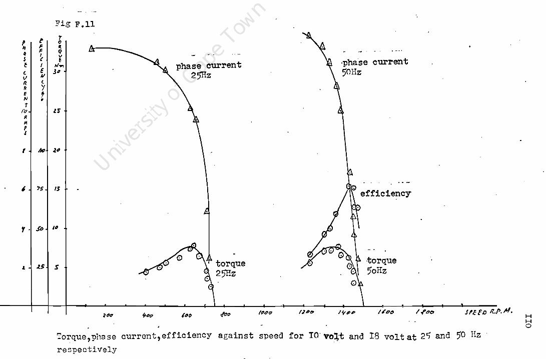
Fig F.ll
~ /I S f <: \I n R E N T
((7
1/ ~ P J
t b F ~ p CO' I v ( ~ I IJ.", E 36 1/ C. 'I ~ ,
lS"
I -I M~ z~
I J '$ -I IS
,. _I $0 J III
~ -i .zs ~ S
B
~
~
l()(? ~(7
phase current 25'Hz
\
,~()
torque 25Hz
~o IfJ~(1 12~t?
·pha'se current 50Hz
~ . efficiency
I 'lIP e>
.torque 50Hz
1#'&1" I "'~O JPfEIJ R.P.H.
Torque, pha se current, efficiency against speed for TO' vo~t and 18 volt at 2t) and 50 Hz '
respectively
H H o

f It 1/ J E
(
v Ii Il
F Ai
1
A .41 f S
Fig F.I2
JC
I I ~ .~urrent i-. T2.,Hz
6 volts
It) 1 r lSI ~e current 6 Hz -0 6 volts R 9J V J.D ~
J' E (fJ
Jim
IS' 6'
If)
r /' _\
Torque ~TOrqU" 6 liz - [2. 5Hz ~ ~ S -I ~ 6 Volts (.) 6 Volts
o 100 200 .300
Torque and phase current against speed for 6 volt batterJ supply at 6 and T2.5H~ '!-Co H
H H

112
Fig. F.,I3
t 0 8/8 r q u 12. e 7/8
-E:J;-'-~.
N/m 6/8 B 5/8
I~OO IS~
speed r.p~.m.
Torque sneed' 'characteristic at 30 volt battery supply and 50 Hz inverter frequency for different mark to space ratios

Magnetizing curves for 50 Hi!: are shown in Pig F }14
Torque speed characteristics at 50 Ht and 75 volts per
phase is shown in Figure F.15 The reason for choosing
75 volts is that the average voltage corresponds to
30 volts for the 9 phase invertor fed induction motor.
vph = 30 x 8/9 x 3 1.11 x .955
= 75 volts
(e) Comparison of 9 Phase Invertor Fed Motor with
3 Phas8 Sinusoidally Fed
The comparison between the 9 phase interlaced invertor
fed induction motor with the 3 phase connected sinus-
oidally fed induction motor was made at 50 Hl and at
the same equivalent average voltage per conductor.
The power output of each phase of the 9 phase invertor
was measured and the total was taken as the input power
to the induction motor. The shaft output torque and
speed were recorded and the mechanical power output
calculated. The test was made at 30 volts battery
voltage and 50 H~ fundamental frequency of the invertor.
The mechanical output power was plotted against input
power of the motor when varying the load with a swinging
type dynamometer. A similar test for 3 phase sinus
oidally fed at 75 volt perprrase and 50 Ht was made,
and compared on the same graph (see Fig F.16).
113

Fig F.14
V .300 0
L
"T
P f.-
Ro
P l.OO
J.I II S E
100
2. 3 q. s o 7 ! PHIJJE C VI<IiEA/7 //Up'
l1agnetizing curves for motor connected as 3 phase and s:i:nusoiaally fed
.;,
, If:) H H ..po..

Fig F.15 ;
~ ., ()
t ~ ,3'phase p } t _ Yeffie'ieney I t ,
I t ~ 11m t \\9 phase overall V So /0 efficiency G
y
sl - /'" / I 3 phase torque ~ '\ J phase torque
, loS
Ole
I "foe
.{ PEEP i? . 1'..-"1.
r
1(1
If
Torque and efficiency versus speed- for 3 phase sinUsoidally"fed 9 phase invert fed induction ~otor at ;n nz and 7;and 3n volt respectevely.
--~--
H H VI

,
F-ig F.17
/If)(J
f 1000
, LJ E I( &00
0 ~
/0 u r
.~ f 'DO /3 phs.oe cJ /", r /
tDo 1 /
_L9 ,/se inverter' fed
/ /
1.00 J / (jI
/
lOO ~ tOf) .3()() .}COo ._ 12tH) ,'!Of) !IOQ
Pm'Ter output versus pO'tver input for 3 phase sinusoidally fed 50 Hz 75v
aIld 9 phase inverter fed 'SOliz , 30 v.
I~t) ?oo/.e/f /A/,PC/T W~TTS
(19:#/'J J
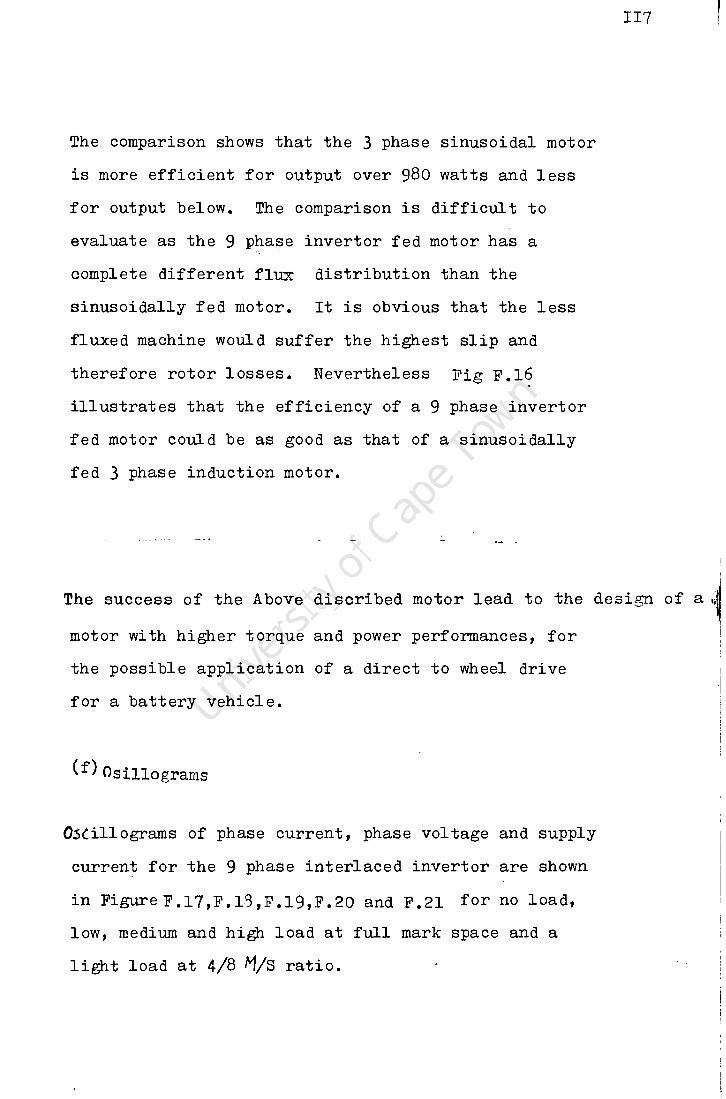
The comparison shows that the 3 phase sinusoidal motor
is more efficient for output over 980 watts and less
for output below. The comparison is difficult to
evaluate as the 9 phase invertor fed motor has a
complete different fl1L~ distribution than the
sinusoidally fed motor. It is obvious that the less
fluxed machine would suffer the highest slip and
therefore rotor losses. Nevertheless Fig F.l6
illustrates that the efficiency of a 9 phase invertor
fed motor could be as good as that of a sinusoidally
fed 3 phase induction motor.
117
The success of the Above discribed motor lead to the design of a,~ motor with higher torque and power performances, for
the possible application of a direct to wheel drive
for a battery vehicle.
(f)Osillograms
OScillograms of phase current, phase voltage and supply
current for the 9 phase interlaced invertor are shown
in FigureF.l7,F.l3,F.l9,F.20 and F.2l for no load,
low, medium and high load at full mark space and a
light load at 4/8 Mis ratio.
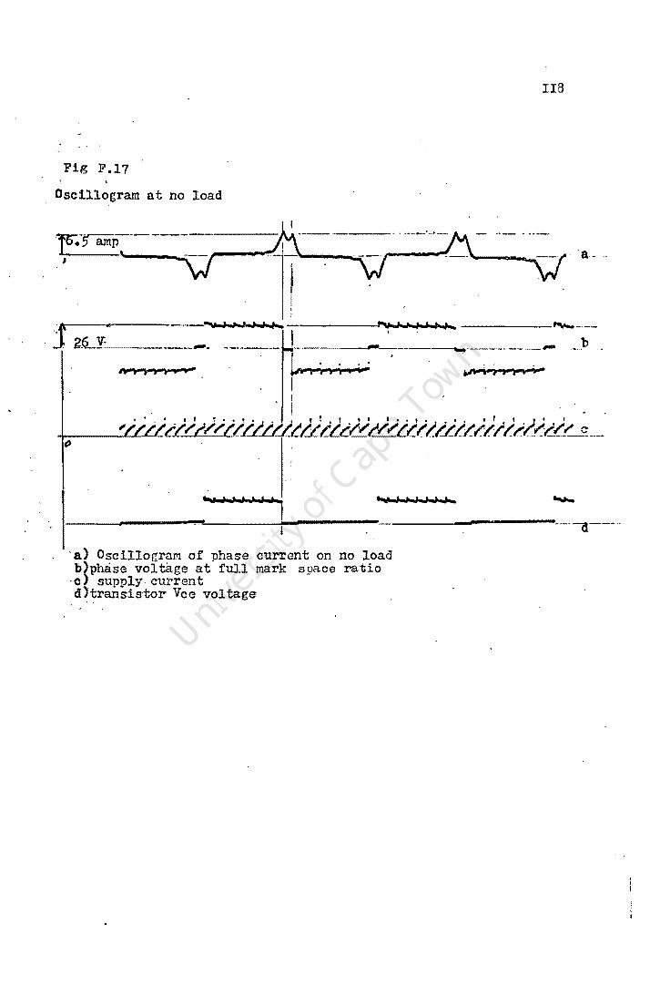
118
Fig P.17
Oscillogram at no load o 0
&-
I "Vai h' ., I.h ... .,tJ .... ~ L .... ____ ----'!....------!oi_-----... : -'-.. --.. --'---------.-.---a--- .. I
°a) Oscillogram of phase current on no load b)phase voltage at full mark space ratio
-0), supply· ourrent d >transistor Vee voltage

Fig F.18 119
. --
(Q..)
~/W~Tr ... ~,-.-_. _"'-_ .. _ ... -_-._ ..... _-_~======~~~...I!!_~~_._;..._;...,_:....._~_~_. __ . ____ -_---'--~~~: __ _
• : I
>0 ...... ]"'/1 IIII'! 1'1 If I' I' II 11/11 /N I 1'1111' 1'1111'1/11 IN I' ~~-~~
(>
Oscillogram for'medium load Torque; T0!Tm, speed 14oo r.p.m. OUtput :I.52 KH.overall efficiency 7J %, motor alone 76~ a) phase current b)phase volta!'!e _a.1supply _ current
{ FigF.19
-~_ . ...,;,..""... . ~------v .. :..;. ~~------~~ ......... -~-.I., .n;lJ 1 ______ ,_------------..:.... ........ ------ .... _
.b)
. 4.L/-f-t!(-lf//-I'/-/-/(/'/I'/'I'/-IIf./-I///II-//t'-I'-L/'//-/-/-/-f-.I-//.. .. __ . a~ 0
D
Osc1.l1o(tram for a)Phnso current b)pha~c voltar,o c)sUlJPly current

Fi~ F.20 120
~ -_.- '~--.. .'. ..' ~ ~_'= d ______ ~~ ~C-U- . ___ ial
------ ., -.' .~
CJ:fff!(/f((n1111 (1(// (( (( (( (//((// If ((f( (( (/---(c) . / . • I3D Al/PS
..
Oscillogram for heavY load Torque: 16Nm,speed 1310 r.p.n. Output : 2.25 K"1, overall efficiency 57%,rnotor alone 67r~ a)phase current b)phase volt~.,?e c· > supply curren t
Fig F.21
.tI,:-! ~. ·-N •• ..,~i1\J;jI.." .. ::"~~';(~ ... ~V~NJ'~~:I:,k~~~~ .. ~~'""'._. , y /l1/1'.f . ,
f! -. - .-------. - .
0scilloliran for snaIl load "1hen choppine at 4/8 H/S n) phase current b) phQse volto~e c) supply current

121
APPENDIX ~
Torque Requirement for a Battery Car
As considerations in establishing the acceptable perform~nce
for an electric vehicle is complex and relative to diverse
requirements, the torque required for a suitable small passenger
electrical car was based on an analytical model developed by
the Australian Bureau of Transport Economics in 1974.The
performances are those shown in figure G'.l the aerodynamic drag , coefficient and rolling resistance coefficient are those shown
in figure G.2. The computed drive force, air drag and total
drag for a 3m car of 600kg total running weight which provide
the performances of figure 7.1 are shown in figure G.3. The I '
maximum stalling torque of 1560N is required.
Choosing a wheel diame:ner of 32cm, the torque requirement is
1560xO.16 2
,
= 125Nm per motor.

-u
F o ~ c. e
( II)
().60
o.o/-()
0.20
/()DO
o
I22
Fig G.l Air Drag and Rolling Resistance coefficients.
rolling resistance - -- -- - - - - - - - - - - - - - - - - - - - - - - - - - - - - - -
drag coefficient
. --- . .-- . _ .. -----_ .. -._._. _ .. ---" .- .. ----
60 J'o 100
speed (/Onlh)
Drive Force --- - Air Drag --- Total Drag
---------------~--:::. .... --- :-.,......-. .. ~ ...,.-
- . -" - :... =-....: ::-:: ::-=:--=--=--= =-= :.. - - - -+=~~-~-==~l~:~~~~~~=~~~~---,~or--------~~O.---------,~O o
speed (km/h)
Fig G.2 Force variation 3m car, 600kB.
-.-

\ ! • 1
\ :
G> 0 M "t:I It\ Q til o. >
• I
\ ~ . I
\ ~ • I
\ ~ I . , :
\ \ I \ '\ \. i · \ : \ \ , . \ . \ \ \
o 0 0 It\ C\I .-.. .. ..
\ \ \ . \ . \ \ \ \ \ \ \ \ \ '\' . , .
. " \ M .... Q) .- .... .... ~, ...
t!) I ..l
I I °
I ·1 · · I
. " \ :. ,"', • o. " , . . . " .... '-" '. " e. ••
~ ...... '. ~"' ".
o o ....
o 00
o 0 \0 .:t
o C\I
'.
o
o 00
o l'-
o \0
o It\
123
• {!J

APPENDIX H
Characteristics and eguivalent circuit of the ~
phase connected motor.
Figures H.l,H.2,H.3, give magnetizing, no-load, and
124
short circuit tests for 50Hz. Assuming the same flux density
at 300 volts 50Hz as 75 volts I2.5Hz, the magnetizing and friction
losses are 370 WATTS at 50Hz. Assuming these losses to be prop
ortional to frequency, then the constant losses at I2.5Hz would
be 97.6 WATTS
The equivalent circuit for I2.5Hz is derived from the above
and is given in figure H.~.
Figure H. 't-
Equivalent Circui t For 3 Phase r.~otor At 12. 5Hz.
The maximum efficiency at I2.5Hz is calculated assuming constant
losses equal to copper losses. The maximum efficiency is found
to be 75.I% when delivering 553 WATTS.

I25
N :::r:: 0 U"\
.p ttl
M 0 .p
J.... 0
~ a
IJ.J to ~
Q)
~ .p 0 Q)
\,) § ~
0 0
~ Q)
~ fJl ttl
~ (\")
S-l 0
G-I
Q)
t ;:s 0
tl.O t!
0"'; N
''''; .p Q)
t! ho cd
to: .. ...::.
rl •
:::r::
bD ''''; I!r-t

r ()
1 II L
f ()
w E ~
()
11
AJ o L o II
o
"" f.\ T 1 ..s
Fig H.2 The Load Power VS Voltage at 50Hz
..:!.co
2. SO
2. 0 C
ISO
ICc>
50
So 100 /50 ,2t:J(;) 2 SO 30GJ
PI1'#fE !/Ol. 711d-e

f) J 1St:. .teo II H-O J lI!)l'" 116 E ()
f
y.o~ L
() r w 11 f G J.8IJ R..
E " W
J~~ " II f " /11/1'(.1 T 1'6)JvE~ T f /
/ r f( I.rO / .s f t!J/
'H 7 J1 / j " E 1lf1(J- fiJ
/ .z C10.J / /
/ /'
/
" I!)(J J $"1> -I /
/,e /'
/' /'
-,.,.. ~ --0 I 1£- ---I I
10 20 s- IS" IlIYlP / 1'/-1111"£
H Ftg H.3 Short Circuit Tests • Voltage VS Current and Input I\l
-J
Power VS Current

128 REFERENCE..§.
I. Electronics and Power. June 1977 pg 474:-'Recent Advances
in Smdium Sulphur Technolmgy!
2 Electric Vehicle I974 pg I~9-I54 :- Special report
'Waiting for a Super Battery'.
3 Electr(>nics and Power.February 1974 pg 125-123 :- 'Some
Hybrid Propulsion Systems for Road Vehicles.'
4 Electrical Review. 2 May 1975 :- 'Fuel Economy Through
]a ttery Power.'
5 Transactions:The S.A. Institute of Electrical Engineers.
February 1973 :- 'A Review of the current status and
future prospects of battery powered electric road vehicles.'
6 Electrical Vehicle. 1974 pg 129,134. :- Special Report 'D.C.
now, A.C. later ?'
7 Tramsmission. 1974 'Special Report. Electric Vehicles.'
8 J.D. van Wyk and J.S. Schoeman. Rand Akrikaans University
Johannesburg. :- The Application of Transistorised Switches
to D.C. and.A.C. machines, for the control of Battery
Veh,icles. '
9 IEEE Transaction on Power Apparatus and Systems. Vol PAS-33,
No 2, February 1969. :- 'The G.m High Performance Induction
r;~otor Drive System.'
10 Electric Vehicle. 1974 pg 126. :- Special Report 'Engineers
In, Stylists Out.,
II Electrical Review International. Vol 200,No 19, 8 April I977
Commentary 'The Viest needs Electric Cars.'
12 Proceedings of the IEBE, vol 60, No 12, December 1972,
pg I523,I525,I526. 'Considerations in the Desi~n of Drive
Systems for On-The-Road Electric V8hiclc8.'
13 Proccedings of the IEE,vol 116, Na9, August 1969. :-

129
Performance and Design of Induction rfJotors with Square Wave
Exi tation. '
14 C.D. Schauder. Electrical Engineering Department, University
of Cape Town:-'The Performance of Squirrel Cage Induction
Motors when exited with variable frequency.'
15 Vector. September 1976, pg 27 :- 'Solid State Control of
A.C Induction ~otors.'
16 Electric Vehicle 1974 pg I39.:-Snecial Report 'How many
speeds, E V Transmissions?'
17 B.D. Bedford Principle of Inverter 0uircuit
Senior electrical Engineer1 Schenectady,New York
18 Electric Vehicle 1974 pg I36.:-Special Report 'SemiConductors
mean extra Range.'
19 Pulse November 1977 pg 74. 'Switching MediulIl Power Loads
with Transistors;-' . 20 IEEE Spectrum August 1977 pg43. 'Power Semiconductors -
Lo oking Ahead. '
21 Electronic Design, February 1.5 I977,pg 94 :-'Use Equations
to Parrallel Transistors.'
22 Electronic Design November 8 I977,pg 23 :-'Focus on
Transistors and Thyristors.'
23\ Conference No 154, 27-29 September 1977 on Power Electronics,
Power Semiconductors, and their apr-lications. :-' High
Voltage, High Power Inverters' Research and Development
Division, British Railv3Ys Board, U.K.
24 Oonference No 154, 27-29 September 1977. :-' High POI/,'er
Transistor Inverters for A.C Drives.' 3rentford Electric
Lind ted pg 92.
25 Electronic Design 4, February 15 1977. :-' Driving Inductive
Loads?'
115 SEP 1978


