Download - The ATLAS inner detector
Steinar Stapnes, LHCC June 2004 1
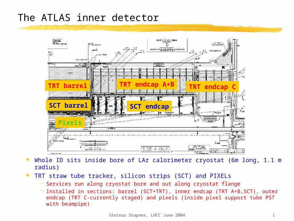
The ATLAS inner detector
TRT endcap A+B TRT endcap CTRT barrel
SCT barrel SCT endcap
Pixels
Whole ID sits inside bore of LAr calorimeter cryostat (6m long, 1.1 m radius) TRT straw tube tracker, silicon strips (SCT) and PIXELs
Services run along cryostat bore and out along cryostat flange Installed in sections: barrel (SCT+TRT), inner endcap (TRT A+B,SCT), outer endcap
(TRT C-currently staged) and pixels (inside pixel support tube PST with beampipe)
Steinar Stapnes, LHCC June 2004 2
Pixel status
The rad-hard electronics being out of the list of the critical parts, we now face the challenge to produce the large number of modules needed with the necessary yield and in 15 months.
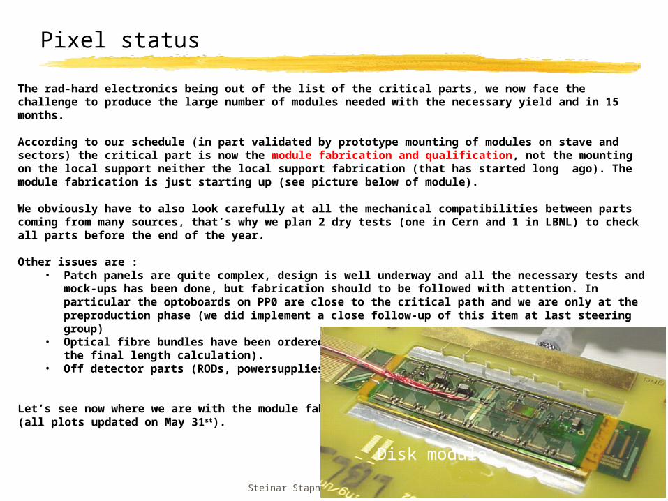
According to our schedule (in part validated by prototype mounting of modules on stave and sectors) the critical part is now the module fabrication and qualification, not the mounting on the local support neither the local support fabrication (that has started long ago). The module fabrication is just starting up (see picture below of module).
We obviously have to also look carefully at all the mechanical compatibilities between parts coming from many sources, that’s why we plan 2 dry tests (one in Cern and 1 in LBNL) to check all parts before the end of the year.
Other issues are : • Patch panels are quite complex, design is well underway and all the necessary tests and mock-ups has been
done, but fabrication should to be followed with attention. In particular the optoboards on PP0 are close to the critical path and we are only at the preproduction phase (we did implement a close follow-up of this item at last steering group)
• Optical fibre bundles have been ordered, cables order will be done soon (need to know the final length calculation).
• Off detector parts (RODs, powersupplies, etc) are making good progress
Let’s see now where we are with the module fabrication(all plots updated on May 31st).
Disk module

Steinar Stapnes, LHCC June 2004 3
Overview bistave with pigtail and type 0 cable bundle

Steinar Stapnes, LHCC June 2004 4
Loading…
Shown below is a source scan of a module on a stave (see components and also some detail of the flex circuit, but no bump damage due to the mounting process).
We plan to start loading of production modules to production stave and sectors before the end of July.
Steinar Stapnes, LHCC June 2004 5
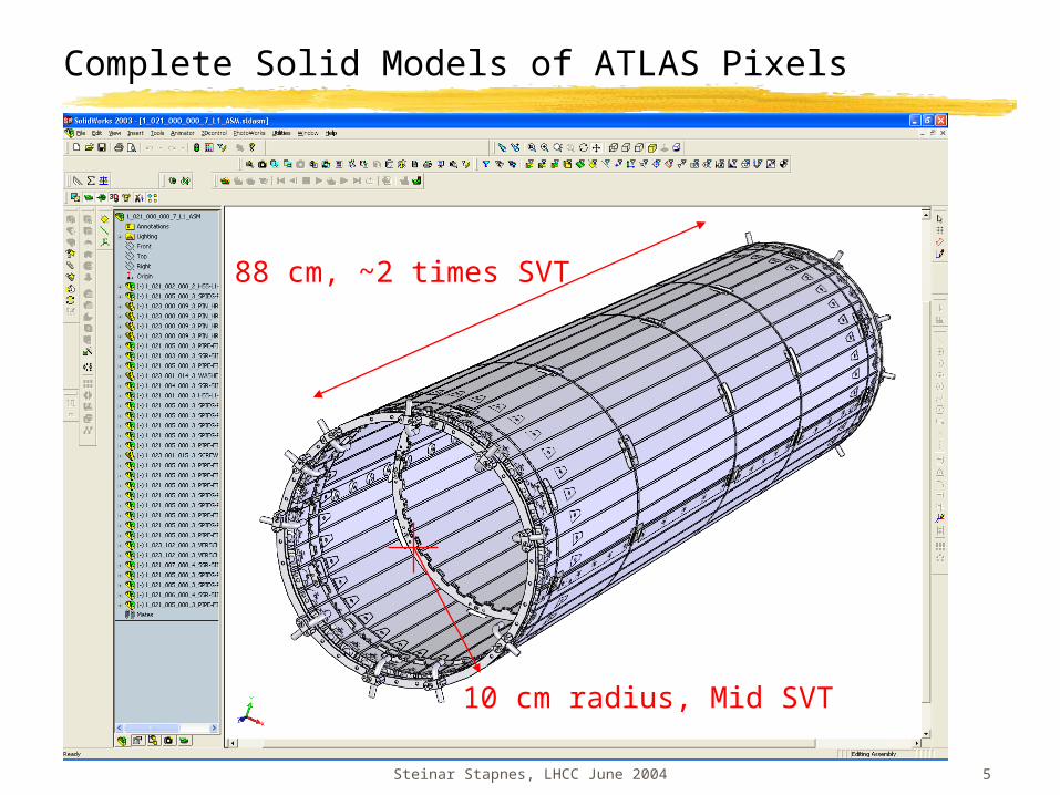
Complete Solid Models of ATLAS Pixels
10 cm radius, Mid SVT
88 cm, ~2 times SVT

Steinar Stapnes, LHCC June 2004 6
Cost of SVT replacement with ATLAS Pixel Modules
Cost of ATLAS Pixel Modules $1000 or $3000 Area of ATLAS Pixel Modules 18 mm 62 mm Area of SVT ~0.8 m2
2.1M$ @ 3k$/module
Steinar Stapnes, LHCC June 2004 7
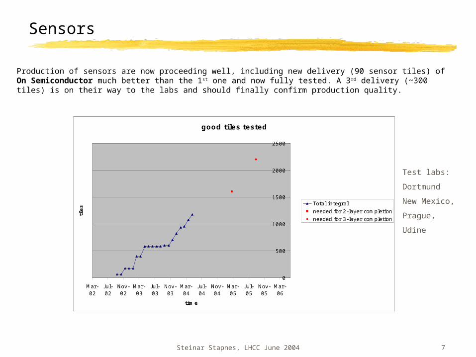
Sensors
Production of sensors are now proceeding well, including new delivery (90 sensor tiles) of On Semiconductor much better than the 1st one and now fully tested. A 3rd delivery (~300 tiles) is on their way to the labs and should finally confirm production quality.
good tiles tested
0
500
1000
1500
2000
2500
Mar-02
J ul-02
Nov-02
Mar-03
J ul-03
Nov-03
Mar-04
J ul-04
Nov-04
Mar-05
J ul-05
Nov-05
Mar-06
time
tile
s
Total integral
needed for 2-layer completion
needed for 3-layer completion
Test labs:
Dortmund
New Mexico,
Prague,
Udine

Steinar Stapnes, LHCC June 2004 8
Front-end electronics
102 8” wafers already delivered (out of 246 ordered) and 54 tested. 48 wafer deliveries are scheduled each 2 months and therefore expect to have all in hand before the end of the year. Testing speed (LBNL+Bonn) very rapidly at cruise speed and agrees with schedule
good dies on wafer
0
5000
10000
15000
20000
25000
30000
35000
40000
45000
Mar-02
Jul-02
Nov-02
Mar-03
Jul-03
Nov-03
Mar-04
Jul-04
Nov-04
Mar-05
Jul-05
Nov-05
Mar-06
month
die
s
Total chips
needed for 2-layer completion
needed for 3-layer completion
Steinar Stapnes, LHCC June 2004 9
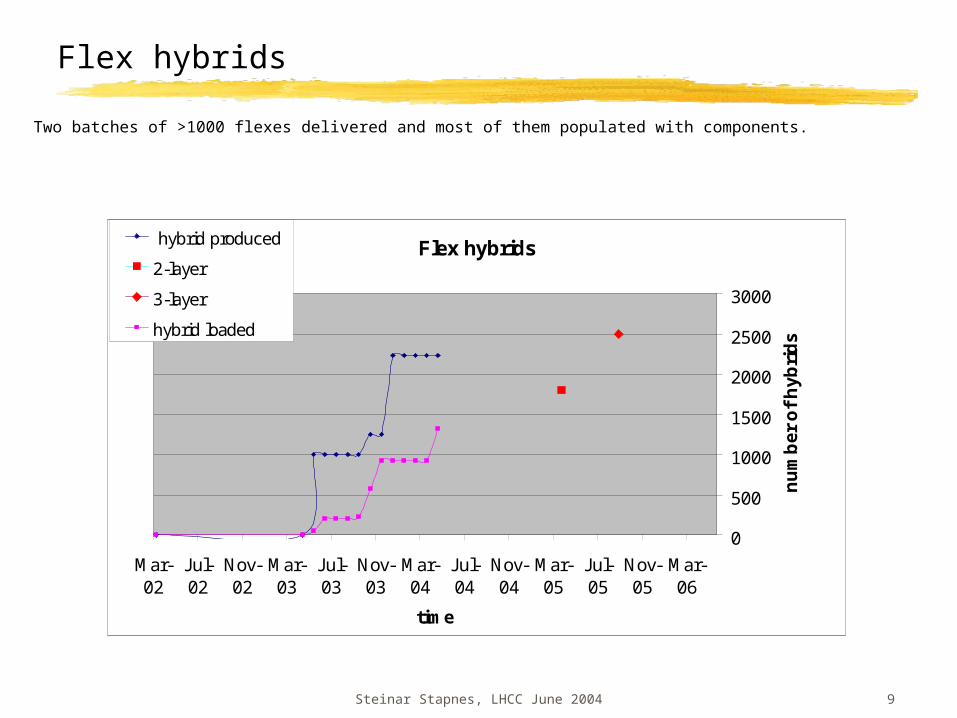
Flex hybrids
Two batches of >1000 flexes delivered and most of them populated with components.
Flex hybrids
0
500
1000
1500
2000
2500
3000
Mar-02
Jul-02
Nov-02
Mar-03
Jul-03
Nov-03
Mar-04
Jul-04
Nov-04
Mar-05
Jul-05
Nov-05
Mar-06
time
nu
mb
er
of
hy
bri
ds
hybrid produced
2-layer
3-layer
hybrid loaded

Steinar Stapnes, LHCC June 2004 10
Modules (qualified and ready to go on the experiment)
We have qualified 3 sites for the module production (Bonn, Genova, LBNL) and three more will shortly follow.
The bumping start-up has been a bit longer than hoped for due to a the need for a key machine repair (now done) in one of the 2 bump vendors.
The production of pixel modules still in the learning curve. We must work on this issue and have the curve ramp-up in the next couple of months.
Flex modules
0
250
500
750
1000
1250
1500
1750
2000
Mar-02
Jul-02
Nov-02
Mar-03
Jul-03
Nov-03
Mar-04
Jul-04
Nov-04
Mar-05
Jul-05
Nov-05
Mar-06
time
nu
mb
er
of
mo
du
les
flex done
flex trahed
2-layer
3-layer
Steinar Stapnes, LHCC June 2004 11
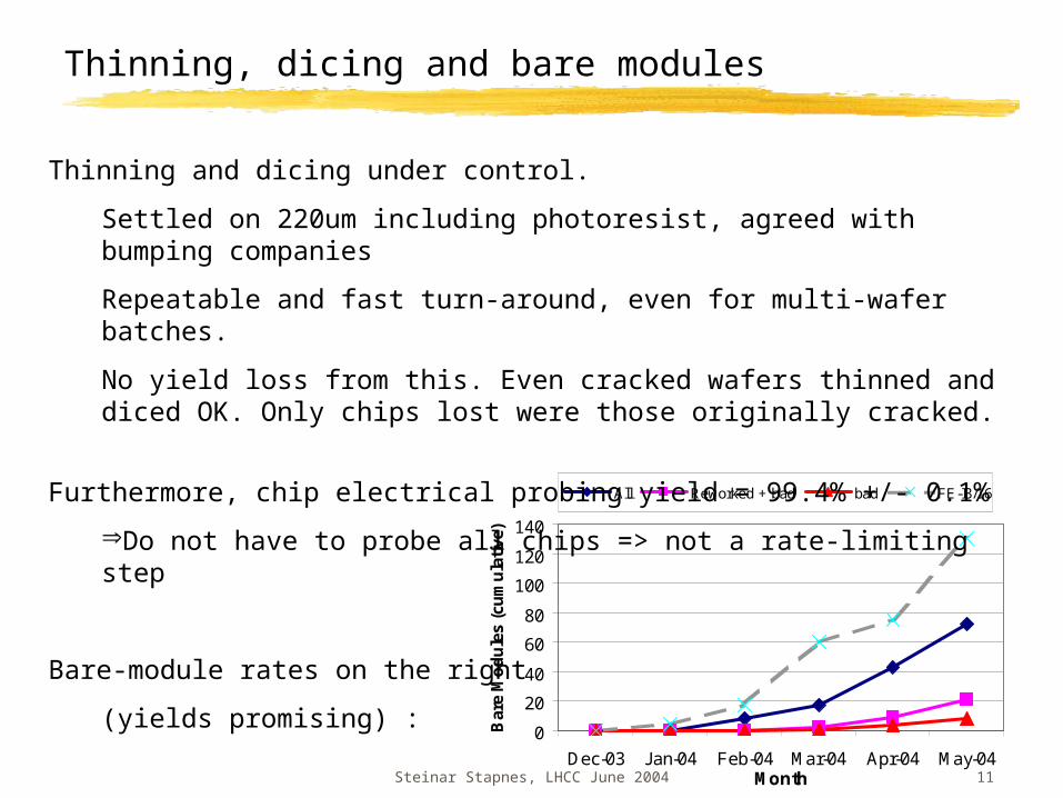
Thinning, dicing and bare modules
0
20
40
60
80
100
120
140
Dec-03 Jan-04 Feb-04 Mar-04 Apr-04 May-04Month
Bar
e M
od
ule
s (c
um
ula
tive
)All Reworked + bad bad FE-I3/16
Thinning and dicing under control.
Settled on 220um including photoresist, agreed with bumping companies
Repeatable and fast turn-around, even for multi-wafer batches.
No yield loss from this. Even cracked wafers thinned and diced OK. Only chips lost were those originally cracked.
Furthermore, chip electrical probing yield = 99.4% +/- 0.1%
Do not have to probe all chips => not a rate-limiting step
Bare-module rates on the right
(yields promising) :

Steinar Stapnes, LHCC June 2004 12
PIXEL schedule
Being lowered with beampipe in July 2006. Component stock is building up and preliminary yield are
promising The critical parameter is module production we have to see
how this turns on …


