
TF Silicon Status and OutlookBeyond the metric EfficiencyEdward Hamers (HyET Solar), Arno Smets (TU Delft)
22-6-2017 Final

Glass based PV in urban environment
2
➢ Utilization of available area is limiting factor

Imagine a PV product ….
✓ Lightweight✓ Flexible✓ Custom-sizing✓ Easy to integrate✓ Low cost
➢ Optimal area coverage

Unique technology enables a unique product
Flexible in shape and size
Light-weight (600 gr/m²)
Ultra flexible
✓ Reinforcement of roof structures not necessary
✓ Dimensions of covered objects do not change
✓ Creation of aesthetic and low cost building solutions
✓ Module characteristics do not restrict architectural creativity
4
Ultra thin (0.5 mm)

5
Pr1: Front contact Pr2: Silicon Pr3: Interconnection Pr4:BackContact
Pr5: Lamination Pr6: Etching Pr7: Encapsulation Pr7: Quality Control
HyET Solar Foil: Production equipment
Production scale Production scale Production scale
Pilot scale Production scale Production scalePilot scale
Pilot scale
➢ Pilot scale: 350 mm, 1-10 MWp/yr ; Production scale:1400 mm width, 25-50 MWp/yrTRL typically 6-7

Unique selling points of TF-Si
•Roll-to-roll manufacturing
•Low material costLowest cost
•Abundant materials used
•Compatible with regulations
•Moisture resistant TCO SnO2 and absorber layer
Abundant materials
•Shadowing of part of module is in general not dramatic for performance Shadowing
•More sensitive to larger angles as light in coupling improves
•Low light performance is goodDiffuse light
•Temperature coefficient is relatively low Temperature
Dif
fere
nce
ST
C a
nd
RO
C

Product reliability
7
✓ Product passes IEC
Meaning a.o.– Accelerated Lifetime testing
– Hailstones
– Cut susceptibility
– Fire testing
– Own outdoor monitoring

Robust and reliable product, eg.
Cut Susceptibility
• Safety aspect
Unencapsulated Damp Heat
• Hot Moisture resistant to >>1000h
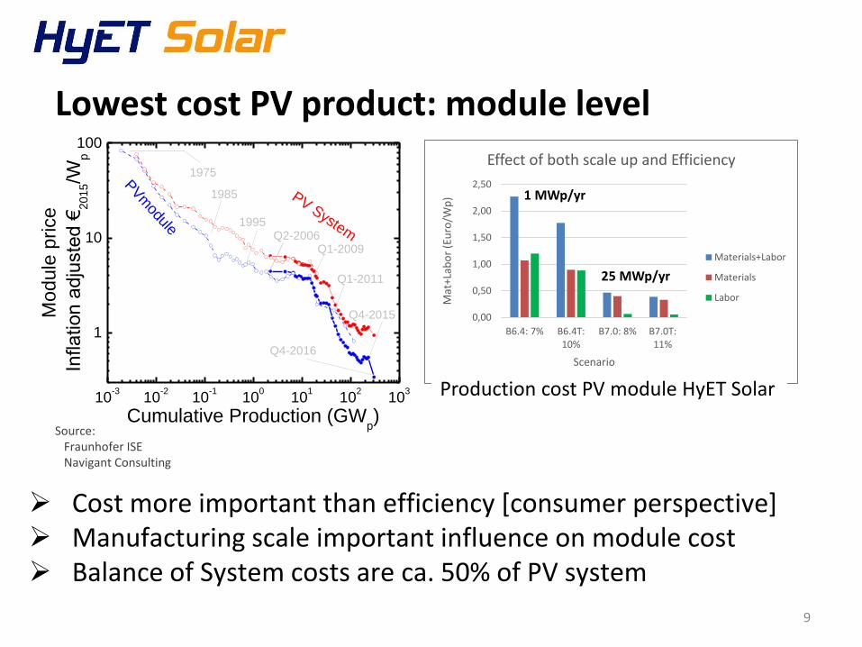
Lowest cost PV product: module level
9
➢ Cost more important than efficiency [consumer perspective]➢ Manufacturing scale important influence on module cost➢ Balance of System costs are ca. 50% of PV system
10-3
10-2
10-1
100
101
102
103
1
10
100
Q4-2016
1995
1985
1975 PVm
odule
Q4-2015
Q1-2011
Q1-2009
Module
price
Inflation a
dju
ste
d €
2015/W
p
Cumulative Production (GWp)
Q2-2006
PV System
Source: Fraunhofer ISE Navigant Consulting
0,00
0,50
1,00
1,50
2,00
2,50
B6.4: 7% B6.4T:10%
B7.0: 8% B7.0T:11%
Mat
+Lab
or
(Eu
ro/W
p)
Scenario
Effect of both scale up and Efficiency
Materials+Labor
Materials
Labor
1 MWp/yr
25 MWp/yr
Production cost PV module HyET Solar

Lowest cost PV product: system level/BoS costs
Flexible in shape and size
Light-weight (600 gr/m²)
Ultra flexible
✓ Reinforcement of roof structures not necessary
✓ Dimensions of covered objects do not change
✓ Module characteristics do not restrict architectural creativity
10
Ultra thin (0.5 mm)
Large modules (>10 m2) reduces Cabling in BoS
Integration saves on Installation BoS
Low weight saves on installation BoS and Light-weight and low volume saves on transport in BoS
✓ Creation of aesthetic and low cost building solutions

Lowest cost PV product: system level/BoS costsBAPV: applied on the roof BIPV: applied in the factory
BoS costs: Mechanical installation0.20 €/Wp (7%) same as c-Si 16%
BoS costs: Mechanical installation<0.05 € /Wp (@ 7%)
➢ Reduction of about 30% on total BoS costs wrt conventional c-Si modules
➢ Flexible product makes huge savings already at low efficiency

Lowest cost PV product: system level/BoS costs
24 m long monolithically
integrated module: 470 Wp
Design: 2 x 10 m long modules on
roofing membrane in
series: 610 Wp
➢ Very large area >1 kWp modules possible ➢ Applications: airport terminals, large industrial buildings, land fills

Energy production compared
22-6-2017 Final

LCOE compared: power plant 8%
22-6-2017 Final

Efficiency Roadmap
Future technology generations (Si & Roll to Roll based) to guarantee continued leadership
Now: €/Wp
➢ Single junction amorphous Si: approx. 8% 0.43
➢ Tandem junction amorphous / microcrystalline Si: approx. 11 % 0.35
Future:
➢ (2017) Tandem junction amorphous/microcrystalline Si (current processes): 11% - 12% 0.32
➢ (2018) Tandem junction amorphous/microcrystalline (NG – SiH4/SiF4): 13 + % 0.31
➢ (2019) Triple junction amorphous/microcrystalline / TF c-Si: 15 + % 0.28
➢ (2019) Triple junction amorphous/microcrystalline / SiGe: 18 - 20% 0.22
➢ (2020) Tandem junction microcrystalline/perovskite: 15 + %
Note: all largely possible to manufacture with existing factory equipment
15

Product Co-Development along the value chain
Pilot Production& Manufacturing through own
and licencees & marketing
Co Development Partners
Front End
Joint Venture Partner
Back End
Innovation Multiplier by involving partners in
the development, manufacturing, sales and
marketing of final products
Equipment suppliers
Material suppliers
Know-how partners Installer
?Clients
Installer
?
Installer
?FundingLocal KnowledgeLarge Scale ManufacturingManufacturing development
marketing

Large area markets with medium gross margin • Roofing Membranes
– Homes
– Large buildings
• Corrugated plates
– Farms
– Developing countries
• Landfills:
– Covering Landfills
• Truck manufacturers
– Spoilers
– Trailers
Bring the sun to the built environment

HOW TO FURTHER REDUCE LCOE: INCREASE EFFICIENCY
22-6-2017 Final

Record single junction TF Si solar cell [AcAS]
• after 1000 h light soaking• subsequently attached anti reflection foil• solar cell area definition by laser scribing➢ Different groups achieved similar efficiencies
0.0 0.2 0.4 0.6 0.8
-15
-10
-5
0
= 10.26%
FF = 67.0%
Voc
= 0.891 V
Jsc
= 17.2 mA/cm²
A = 1 cm²
cu
rre
nt
de
nsity J
[m
Acm
-2]
voltage V [V]
A. Lambertz et al. (submitted 2015)
0.0 0.3 0.6 0.9 1.2 1.50
2
4
6
8
10
12
14
16
Cu
rrent D
ensity (
mA
/cm
2)
Voltage (V)
Voc=1.424 V
Jsc =14.0 mA/cm2
FF =74.4%
Eff =14.8%
a-Si:H
nc-Si:H
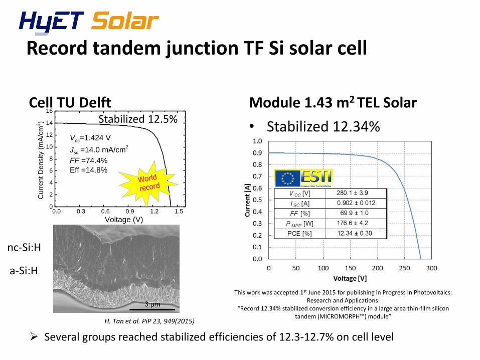
H. Tan et al. PiP 23, 949(2015)
Record tandem junction TF Si solar cell
Stabilized 12.5%
➢ Several groups reached stabilized efficiencies of 12.3-12.7% on cell level
Cell TU Delft Module 1.43 m2 TEL Solar
• Stabilized 12.34%
This work was accepted 1st June 2015 for publishing in Progress in Photovoltaics: Research and Applications:
“Record 12.34% stabilized conversion efficiency in a large area thin-film silicon tandem (MICROMORPH™) module”

21
14.04%
H. Sai et al. APL 183506 (2016)
Record triple junction TF Si [AcAS]

22
Hybrid PV Structures
T3
T4
T1
T2
Mildly textured front TCO
AZO
Ag/MoO3
PMDPP3T:PC6
0BM
LiF/Al/Ag
a-Si:H p-i-n front
a-Si:H p-i-n middle
glass
2,3,4-j: c-Si/ TF Si Hybrids for high voltage
1j a-Si/c-Sihetero-junction
2j 4-terminal (4T)/4T - spectral splittinga-SiOx:H/c-Si
2j a-Si:H/nc-Si:H4j a-SiO:H/a-Si:H/
nc-Si:H/nc-Si:H
3j a-Si:H/a-Si:H/OPV
2j a-Si:H/CIGS
2,3,4-j: c-Si/ TF Si for solar-to-fuel:

Efficiency Roadmap
Future technology generations (Si & Roll to Roll based) to guarantee continued leadership
Now:
➢ Single junction amorphous Si: approx. 8%
➢ Tandem junction amorphous / microcrystalline Si: approx. 11 %
Future:
➢ (2017) Tandem junction amorphous/microcrystalline Si (current processes): 11% - 12%
➢ (2018) Tandem junction amorphous/microcrystalline (NG – SiH4/SiF4): 13 + %
➢ (2019) Triple junction amorphous/microcrystalline / TF c-Si: 15 + %
➢ (2019) Triple junction amorphous/microcrystalline / SiGe: 18 - 20%
➢ (2020) Tandem junction microcrystalline/perovskite: 15 + %
Note: all largely possible to manufacture with existing factory equipment
23

Status & Roadmap TF SiFlexible TF Si PV modules: next standard in PV production
Next steps: ➢ Secure financing for scale up to 25 MWp/yr in Arnhem and ➢ Develop market for 3-4 international 200 MWp/yr fabs in licence production.
Roadmap• Supply chain raw materials cost reduction especially encapsulation• Towards production tools for GWp/yr production• Towards building element lifetimes 25 yr+• Develop products for large niche applications : GWp scale• Demonstration projects and educate market on possibilities • Educate installers• Further cost reduction: efficiency improvement
22-6-2017 Final

The effect of module temperature
Output in terms of Power
0
50
100
150
200
250
0 20 40 60 80 100 120
P (
Wp
/m2
)
Temperature (°C)
Effect module temperature
P_cSi
P_aSimucSi
P_aSi
Relative wrt STC
60%
70%
80%
90%
100%
110%
120%
0 20 40 60 80 100 120
Rel
ativ
e P
ow
er w
rt S
TC
Temperature (°C)
Effect module temperature
Prel_aSi
Prel_aSimucSi
Prel_cSi
Γrel (%/K)
c-Si -0.45
a-Si:H -0.13
a-Si:H/muc-Si:H -0.33
STC

Technology:Temporary Aluminium ‘superstrate’
Use of substrate Aluminium foil essential
Step 1 : TCO (SnO2:F) at 500°C
Step 2 : a-Si:H & nc-Si:H at 200°C
Step 3 : Back contact
Step 4 : Interconnection
Step 5 : Carrier lamination
Step 6 : Removal Al foil
Step 7 : Encapsulation & Quality Control
➢ Unique high temperature process via Aluminium foil yields an energy efficient, very thin and extremely flexible product
➢ This production advantage eliminates traditional thin film silicon concerns
26
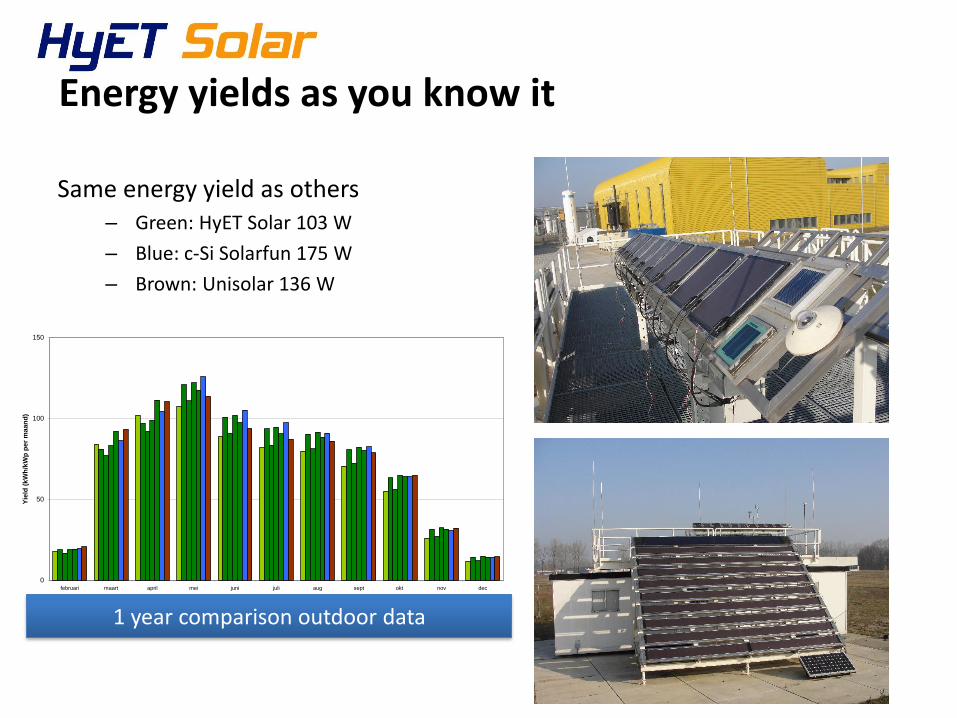
Energy yields as you know it
Same energy yield as others– Green: HyET Solar 103 W
– Blue: c-Si Solarfun 175 W
– Brown: Unisolar 136 W
0
50
100
150
februari maart april mei juni juli aug sept okt nov dec
Yie
ld (
kW
h/k
Wp
per
maan
d)
Helianthos 2 * 53 Wp Helianthos 2 * 103 Wp (1) Helianthos 2 * 103 Wp (2)
Helianthos 2 * 103 Wp (3) Helianthos 2 * 103 Wp (4) c- Silicium referentie (Solarfun 175 Wp)
a-Si triple junction referentie (Unisolar 136 Wp)1 year comparison outdoor data

Improved IR absorption in nc-Si:H from SiF4Increase bottom cell crystallinity with SiF4 precursor
Q. Zhang, PSS-RRL 2008S. Hänni, Ph.D. Thesis EPFL 2014
32 mA/cm2
➢ > 15 mA/cm2 matched, ➢ Potential (assuming 71% FF and 1.4 V): η ≈ 15%
EPFL PV-Lab
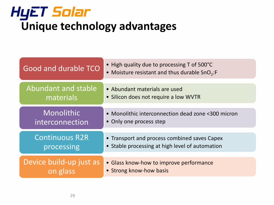
Unique technology advantages
29
• High quality due to processing T of 500°C
• Moisture resistant and thus durable SnO2:FGood and durable TCO
• Abundant materials are used
• Silicon does not require a low WVTR
Abundant and stable materials
• Monolithic interconnection dead zone <300 micron
• Only one process step
Monolithic interconnection
• Transport and process combined saves Capex
• Stable processing at high level of automation
Continuous R2R processing
• Glass know-how to improve performance
• Strong know-how basis
Device build-up just as on glass

Excellent Lifetime stabilityDamp Heat (85ºC, 85% RH) Stability
a-Si:H and a-Si:H/µc-Si:H
0.0
1.0
2.0
3.0
4.0
5.0
6.0
7.0
8.0
9.0
10.0
0 500 1000 1500 2000 2500 3000 3500 4000 4500
Testing Time (h)
Eff
icie
nc
y (
%)
roll-to-roll a-Si:H 28x30 cm² modules
batch tandem 5x5 cm² modules
IEC norm
testing time
➢ Lifetime is combination of PV layer technology used and the encapsulation system

Status PV technologies: upscaling to production
Courtesy: Arno Smets
➢ Thin Film silicon seems to be the technology that is scaled up the easiest
0.1 1 10 100 1000 100000
4
8
12
16
20
24
28
32
36
40
1j-organic PV
(not stabilized)
1j-perovskite (not stabilized)
3j-InGaP/GaAs/InGaAs
MODULE
WAFER
1j-FZ c-Si: HIT
2j-TF Si
3j-TF Si
1j-CdTe
1j-CIGS
1j-mc-Si
Eff
icie
ncy (
%)
Area (cm2)
1j-FZ c-Si: IBC
LAB CELL
1j-GaAs
10 m2 100 m2
roll-to-roll
Batch
24
m lo
ng,
7 m
2m
od
ule

TF-Si community: R&D activities on efficiency
• Anti-reflection concepts
• Light trapping conceptsAntireflection
• Different TCO’s
• Different surface morphologiesTCO
• Doped SiOx layers to reduce absorptionSingle cell
• Intermediate reflector layers
• SiF4 as precursor in nc-Si:H depositionTandem cell
• Alloys Si-Ge
• Applications for water splittingTriple cell
• Use of n-SiOx doped layer in Back reflectorBack Reflector

Tandem at HyET Solar
Device lay-out Performance
• 5 cm2 cell in module configuration
Voc(V)
FF(-)
JsrToC(mA/cm2)
JsrBoC(mA/cm2)
Eff(%)
Initial 5 cm2 1.325 0.740 11.75 11.10 10.9
20 nm
i-pm-Si:H 300 nm
ZnO:Al 70 nm
SnO2:F
p-a-Si:C:H
Ag 120 nm
n-a-Si:Hn-SiOx:H 60 nm
n- a- Si:H
i-nc-Si:H 1600 nm
a-Si
µ-Si
p-SiOx:H
AR
Native Texture
0.0
0.1
0.2
0.3
0.4
0.5
0.6
0.7
0.8
0.9
300 400 500 600 700 800 900 1000 1100
EQE
(-)
Wavelength (nm)

Light-Induced Water-Splitting using anIntegrated Photoelectrochemical Thin-Film Si Device
Urbain et al., Sol. Energy Mater. Sol. Cells 140 (2015) 275Urbain et al., J. Mater. Res. 29 (2014) 2605Ziegler et al., ChemPhysChem 15 (2014) 4026
Solar-To-Hydrogen Efficiency:
ηSTH = 9.5%
PV Efficiency and Stability Integrated water-splitting device
▪ Multijunction Si thin-film solar cells for water-splitting: Voc up to 2.8 V
▪ Stabilized solar cell efficiency of ηPV = 12.5%
▪ Solar-to-hydrogen efficiency ηSTH = 9.5%
ηPV = 12.5%

How important is efficiency
1. Allows comparison very similar products
2. With similar materials it will lower $/Wp
3. With similar production technology it will lower $/Wp
4. With similar BoS costs it will lower $/Wpsystem costs
➢Efficiency is a very important driver
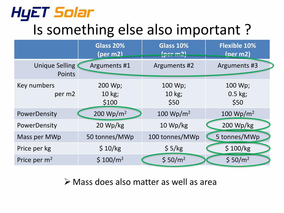
Is something else also important ?Glass 20% (per m2)
Glass 10%(per m2)
Flexible 10% (per m2)
Unique Selling Points
Arguments #1 Arguments #2 Arguments #3
Key numbers per m2
200 Wp; 10 kg; $100
100 Wp; 10 kg;
$50
100 Wp; 0.5 kg;
$50
PowerDensity 200 Wp/m2 100 Wp/m2 100 Wp/m2
PowerDensity 20 Wp/kg 10 Wp/kg 200 Wp/kg
Mass per MWp 50 tonnes/MWp 100 tonnes/MWp 5 tonnes/MWp
Price per kg $ 10/kg $ 5/kg $ 100/kg
Price per m2 $ 100/m2 $ 50/m2 $ 50/m2
➢Mass does also matter as well as area

Increasing production width to 1400 mm
Step 1: TCO
• Roll-to-roll
Step 2: Silicon
• Stationary
38
✓ Thickness 300±2 nm
from 2 cm from edge

Pr1: FrontContact
Pr2: Silicon
Pr3: Interconnection
Pr4: BackContact
Pr5: Lamination
Pr6: Etching
Pr7: Encapsulation
Pr8: Confectioning
Auxiliary Processes
22-6-2017 Final
80 m
150 m
39
Factory lay-out 200 MWp/yr
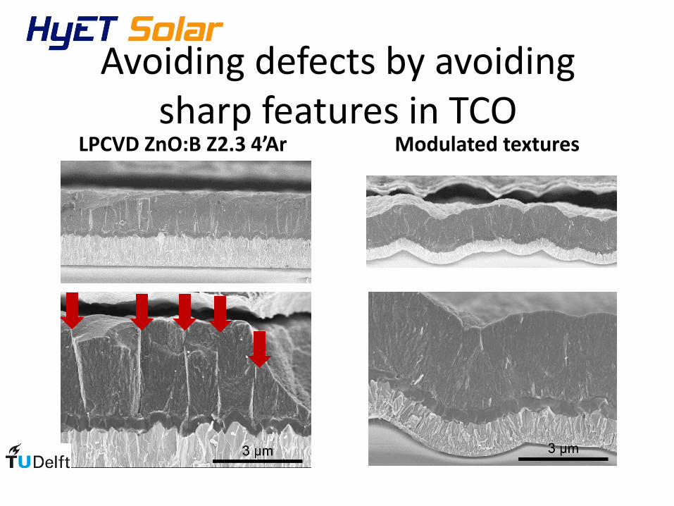
Avoiding defects by avoiding sharp features in TCO
LPCVD ZnO:B Z2.3 4’Ar Modulated textures

Liquid-Phase Crystallized Silicon on Glass
-0.2 -0.1 0.0 0.1 0.2 0.3 0.4 0.5 0.6 0.7-30
-25
-20
-15
-10
-5
0
5
Curr
ent
densi
ty (
mA
/cm
²)
Voltage (V)
1-49-140-133, cell 3
superstrate
Jsc = 27.25 mA/cm²
Voc = 649 mV
FF = 68.4 %
ETA = 12.1 %
• 20/100/80 nm SiN/SiO/SiON• 5-10 µm LPC-Si n-type absorber,• i/p hetero emitter, back-side contact scheme• white reflector + textured AR foil.
O. Gabriel et al., IEEE J-PV 2014
IL stack
5 µm - 40 µm Si precursor layer
glassLPC-Si
e-beam / cw laser
J. Haschke et al., Sol.Mat 2014
D. Amkreutz et al., Prog. PV Res. Appl. 19, 937 (2011)
interlayer
a-Si:H(i/p)
insulatorITO
Ti/Pd/Ag contacts
T. Frijnts et al., submitted


